Embed Size (px)
Citation preview
1
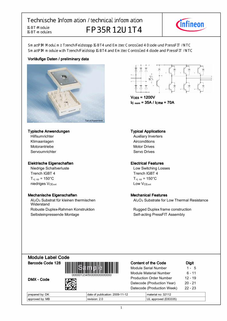
Technische Information / technical information
FP35R12U1T4IGBT-ModuleIGBT-modules
prepared by: DK
approved by: MB
date of publication: 2009-11-12
revision: 2.0
material no: 32112
UL approved (E83335)
SmartPIM Modul mit Trench/Feldstopp IGBT4 und Emitter Controlled 4 Diode und PressFIT / NTC
SmartPIM module with Trench/Fieldstop IGBT4 and Emitter Controlled 4 diode and PressFIT / NTC
Vorläufige Daten / preliminary dataVorläufige Daten / preliminary dataVorläufige Daten / preliminary dataVorläufige Daten / preliminary data
V†Š» = 1200VV†Š» = 1200VV†Š» = 1200VV†Š» = 1200V
I† ÒÓÑ = 35A / I†ç¢ = 70AI† ÒÓÑ = 35A / I†ç¢ = 70AI† ÒÓÑ = 35A / I†ç¢ = 70AI† ÒÓÑ = 35A / I†ç¢ = 70A
Typische AnwendungenTypische AnwendungenTypische AnwendungenTypische Anwendungen Typical ApplicationsTypical ApplicationsTypical ApplicationsTypical Applications
• •Hilfsumrichter Auxiliary Inverters
• •Klimaanlagen Airconditions
• •Motorantriebe Motor Drives
• •Servoumrichter Servo Drives
Elektrische EigenschaftenElektrische EigenschaftenElektrische EigenschaftenElektrische Eigenschaften Electrical FeaturesElectrical FeaturesElectrical FeaturesElectrical Features
• •Niedrige Schaltverluste Low Switching Losses
• •Trench IGBT 4 Trench IGBT 4
• •TÝÎ ÓÔ = 150°C TÝÎ ÓÔ = 150°C
• •niedriges V†ŠÙÈÚ Low V†ŠÙÈÚ
Mechanische EigenschaftenMechanische EigenschaftenMechanische EigenschaftenMechanische Eigenschaften Mechanical FeaturesMechanical FeaturesMechanical FeaturesMechanical Features
• •AlèOé Substrat für kleinen thermischenWiderstand
AlèOé Substrate for Low Thermal Resistance
• •Robuste Duplex-Rahmen Konstruktion Rugged Duplex frame construction
• •Selbsteinpressende Montage Self-acting PressFIT Assembly
Module Label CodeModule Label CodeModule Label CodeModule Label CodeBarcode Code 128Barcode Code 128Barcode Code 128Barcode Code 128
DMX - CodeDMX - CodeDMX - CodeDMX - Code
Content of the CodeContent of the CodeContent of the CodeContent of the Code Digit Digit Digit DigitModule Serial Number 1 - 5
Module Material Number 6 - 11
Production Order Number 12 - 19
Datecode (Production Year) 20 - 21
Datecode (Production Week) 22 - 23
2
Technische Information / technical information
FP35R12U1T4IGBT-ModuleIGBT-modules
prepared by: DK
approved by: MB
date of publication: 2009-11-12
revision: 2.0
Vorläufige Datenpreliminary data
IGBT-Wechselrichter / IGBT-inverterHöchstzulässige Werte / maximum rated valuesKollektor-Emitter-Sperrspannungcollector-emitter voltage
TÝÎ = 25°C V†Š» 1200 V
Kollektor-DauergleichstromDC-collector current
T† = 100°C, TÝÎ = 175°CT† = 25°C, TÝÎ = 175°C
I† ÒÓÑI†
3554
AA
Periodischer Kollektor Spitzenstromrepetitive peak collector current t« = 1 ms I†ç¢ 70 A
Gesamt-Verlustleistungtotal power dissipation
T† = 25°C, TÝÎ = 175°C PÚÓÚ 250 W
Gate-Emitter-Spitzenspannunggate-emitter peak voltage V•Š» +/-20 V
Charakteristische Werte / characteristic values min. typ. max.
Kollektor-Emitter Sättigungsspannungcollector-emitter saturation voltage
I† = 35 A, V•Š = 15 VI† = 35 A, V•Š = 15 VI† = 35 A, V•Š = 15 V
V†Š ÙÈÚ
1,852,152,25
2,25
VVV
TÝÎ = 25°CTÝÎ = 125°CTÝÎ = 150°C
Gate-Schwellenspannunggate threshold voltage
I† = 1,20 mA, V†Š = V•Š, TÝÎ = 25°C V•ŠÚÌ 5,2 5,8 6,4 V
Gateladunggate charge V•Š = -15 V ... +15 V Q• 0,27 µC
Interner Gatewiderstandinternal gate resistor TÝÎ = 25°C R•ÍÒÚ 0,0 Â
Eingangskapazitätinput capacitance
f = 1 MHz, TÝÎ = 25°C, V†Š = 25 V, V•Š = 0 V CÍþÙ 2,00 nF
Rückwirkungskapazitätreverse transfer capacitance f = 1 MHz, TÝÎ = 25°C, V†Š = 25 V, V•Š = 0 V CØþÙ 0,07 nF
Kollektor-Emitter Reststromcollector-emitter cut-off current
V†Š = 1200 V, V•Š = 0 V, TÝÎ = 25°C I†Š» 1,0 mA
Gate-Emitter Reststromgate-emitter leakage current V†Š = 0 V, V•Š = 20 V, TÝÎ = 25°C I•Š» 400 nA
Einschaltverzögerungszeit (ind. Last)turn-on delay time (inductive load)
I† = 35 A, V†Š = 600 VV•Š = ±15 VR•ÓÒ = 12 Â
tÁ ÓÒ
0,0250,0250,025
µsµsµs
TÝÎ = 25°CTÝÎ = 125°CTÝÎ = 150°C
Anstiegszeit (induktive Last)rise time (inductive load)
I† = 35 A, V†Š = 600 VV•Š = ±15 VR•ÓÒ = 12 Â
tØ
0,0130,0160,018
µsµsµs
TÝÎ = 25°CTÝÎ = 125°CTÝÎ = 150°C
Abschaltverzögerungszeit (ind. Last)turn-off delay time (inductive load)
I† = 35 A, V†Š = 600 VV•Š = ±15 VR•ÓËË = 12 Â
tÁ ÓËË
0,240,2950,31
µsµsµs
TÝÎ = 25°CTÝÎ = 125°CTÝÎ = 150°C
Fallzeit (induktive Last)fall time (inductive load)
I† = 35 A, V†Š = 600 VV•Š = ±15 VR•ÓËË = 12 Â
tË
0,1150,170,20
µsµsµs
TÝÎ = 25°CTÝÎ = 125°CTÝÎ = 150°C
Einschaltverlustenergie pro Pulsturn-on energy loss per pulse
I† = 35 A, V†Š = 600 V, L» = 35 nHV•Š = ±15 V, di/dt = 2500 A/µs (TÝÎ=150°C)R•ÓÒ = 12 Â
EÓÒ 1,902,903,15
mJmJmJ
TÝÎ = 25°CTÝÎ = 125°CTÝÎ = 150°C
Abschaltverlustenergie pro Pulsturn-off energy loss per pulse
I† = 35 A, V†Š = 600 V, L» = 35 nHV•Š = ±15 V, du/dt = 3600 V/µs (TÝÎ=150°C)R•ÓËË = 12 Â
EÓËË 2,002,903,20
mJmJmJ
TÝÎ = 25°CTÝÎ = 125°CTÝÎ = 150°C
KurzschlussverhaltenSC data
V•Š ù 15 V, V†† = 800 V V†ŠÑÈà = V†Š» -LÙ†Š ·di/dt
IȠ 130
A
TÝÎ = 150°C
t« ù 10 µs,
Innerer Wärmewiderstandthermal resistance, junction to case pro IGBT / per IGBT RÚÌœ† 0,55 0,60 K/W
Übergangs-Wärmewiderstandthermal resistance, case to heatsink
pro IGBT / per IGBTð«ÈÙÚþ = 1 W/(m·K) / ðÃØþÈÙþ = 1 W/(m·K) RÚ̆™ 0,50 K/W
3
Technische Information / technical information
FP35R12U1T4IGBT-ModuleIGBT-modules
prepared by: DK
approved by: MB
date of publication: 2009-11-12
revision: 2.0
Vorläufige Datenpreliminary data
Diode-Wechselrichter / diode-inverterHöchstzulässige Werte / maximum rated valuesPeriodische Spitzensperrspannungrepetitive peak reverse voltage
TÝÎ = 25°C Vçç¢ 1200 V
DauergleichstromDC forward current
IΠ35 A
Periodischer Spitzenstromrepetitive peak forward current t« = 1 ms IŒç¢ 70 A
GrenzlastintegralI²t - value
Vç = 0 V, t« = 10 ms, TÝÎ = 125°CVç = 0 V, t« = 10 ms, TÝÎ = 150°C
I²t 240220
A²sA²s
Charakteristische Werte / characteristic values min. typ. max.
Durchlassspannungforward voltage
IŒ = 35 A, V•Š = 0 VIŒ = 35 A, V•Š = 0 VIŒ = 35 A, V•Š = 0 V
VŒ
1,651,651,65
2,15
VVV
TÝÎ = 25°CTÝÎ = 125°CTÝÎ = 150°C
Rückstromspitzepeak reverse recovery current
IŒ = 35 A, - diŒ/dt = 2500 A/µs (TÝÎ=150°C)Vç = 600 VV•Š = -15 V
Iç¢ 81,085,088,0
AAA
TÝÎ = 25°CTÝÎ = 125°CTÝÎ = 150°C
Sperrverzögerungsladungrecovered charge
IŒ = 35 A, - diŒ/dt = 2500 A/µs (TÝÎ=150°C)Vç = 600 VV•Š = -15 V
QØ 3,956,807,50
µCµCµC
TÝÎ = 25°CTÝÎ = 125°CTÝÎ = 150°C
Abschaltenergie pro Pulsreverse recovery energy
IŒ = 35 A, - diŒ/dt = 2500 A/µs (TÝÎ=150°C)Vç = 600 VV•Š = -15 V
EØþÊ 1,502,702,95
mJmJmJ
TÝÎ = 25°CTÝÎ = 125°CTÝÎ = 150°C
Innerer Wärmewiderstandthermal resistance, junction to case pro Diode / per diode RÚÌœ† 0,70 0,80 K/W
Übergangs-Wärmewiderstandthermal resistance, case to heatsink
pro Diode / per diodeð«ÈÙÚþ = 1 W/(m·K) / ðÃØþÈÙþ = 1 W/(m·K)
RÚ̆™ 0,65 K/W
Diode-Gleichrichter / diode-rectifierHöchstzulässige Werte / maximum rated valuesPeriodische Rückw. Spitzensperrspannungrepetitive peak reverse voltage TÝÎ = 25°C Vçç¢ 1600 V
Durchlassstrom Grenzeffektivwert pro Dio.forward current RMS maximum per diode
T† = 100°C IŒç¢»¢ 50 A
Gleichrichter Ausgang Grenzeffektivstrommaximum RMS current at Rectifier output T† = 100°C I碻¢ 50 A
Stoßstrom Grenzwertsurge forward current
tÔ = 10 ms, TÝÎ = 25°CtÔ = 10 ms, TÝÎ = 150°C IŒ»¢
450370
AA
GrenzlastintegralI²t - value
tÔ = 10 ms, TÝÎ = 25°CtÔ = 10 ms, TÝÎ = 150°C
I²t 1000685
A²sA²s
Charakteristische Werte / characteristic values min. typ. max.
Durchlassspannungforward voltage
TÝÎ = 150°C, IŒ = 35 A VŒ 0,95 V
Sperrstromreverse current TÝÎ = 150°C, Vç = 1600 V Iç 1,00 mA
Innerer Wärmewiderstandthermal resistance, junction to case
pro Diodeper diode
RÚÌœ† 0,95 1,05 K/W
Übergangs-Wärmewiderstandthermal resistance, case to heatsink
pro Diode / per diodeð«ÈÙÚþ = 1 W/(m·K) / ðÃØþÈÙþ = 1 W/(m·K) RÚ̆™ 0,85 K/W

4
Technische Information / technical information
FP35R12U1T4IGBT-ModuleIGBT-modules
prepared by: DK
approved by: MB
date of publication: 2009-11-12
revision: 2.0
Vorläufige Datenpreliminary data
IGBT-Brems-Chopper / IGBT-brake-chopperHöchstzulässige Werte / maximum rated valuesKollektor-Emitter-Sperrspannungcollector-emitter voltage
TÝÎ = 25°C V†Š» 1200 V
Kollektor-DauergleichstromDC-collector current
T† = 100°C, TÝÎ = 175°CT† = 25°C, TÝÎ = 175°C
I†ÒÓÑI†
3554
AA
Periodischer Kollektor Spitzenstromrepetitive peak collector current t« = 1 ms I†ç¢ 70 A
Gesamt-Verlustleistungtotal power dissipation
T† = 25°C, TÝÎ = 175°C PÚÓÚ 250 W
Gate-Emitter-Spitzenspannunggate-emitter peak voltage V•Š» +/-20 V
Charakteristische Werte / characteristic values min. typ. max.
Kollektor-Emitter Sättigungsspannungcollector-emitter saturation voltage
I† = 35 A, V•Š = 15 VI† = 35 A, V•Š = 15 VI† = 35 A, V•Š = 15 V
V†Š ÙÈÚ
1,852,152,25
2,25
VVV
TÝÎ = 25°CTÝÎ = 125°CTÝÎ = 150°C
Gate-Schwellenspannunggate threshold voltage
I† = 1,20 mA, V†Š = V•Š, TÝÎ = 25°C V•ŠÚÌ 5,2 5,8 6,4 V
Gateladunggate charge V•Š = -15 V ... +15 V Q• 0,27 µC
Interner Gatewiderstandinternal gate resistor TÝÎ = 25°C R•ÍÒÚ 0,00 Â
Eingangskapazitätinput capacitance
f = 1 MHz, TÝÎ = 25°C, V†Š = 25 V, V•Š = 0 V CÍþÙ 2,00 nF
Rückwirkungskapazitätreverse transfer capacitance f = 1 MHz, TÝÎ = 25°C, V†Š = 25 V, V•Š = 0 V CØþÙ 0,07 nF
Kollektor-Emitter Reststromcollector-emitter cut-off current
V†Š = 1200 V, V•Š = 0 V, TÝÎ = 25°C I†Š» 1,0 mA
Gate-Emitter Reststromgate-emitter leakage current V†Š = 0 V, V•Š = 20 V, TÝÎ = 25°C I•Š» 400 nA
Einschaltverzögerungszeit (ind. Last)turn-on delay time (inductive load)
I† = 35 A, V†Š = 600 VV•Š = ±15 VR•ÓÒ = 47 Â
tÁ ÓÒ 0,070,070,07
µsµsµs
TÝÎ = 25°CTÝÎ = 125°CTÝÎ = 150°C
Anstiegszeit (induktive Last)rise time (inductive load)
I† = 35 A, V†Š = 600 VV•Š = ±15 VR•ÓÒ = 47 Â
tØ 0,0450,050,057
µsµsµs
TÝÎ = 25°CTÝÎ = 125°CTÝÎ = 150°C
Abschaltverzögerungszeit (ind. Last)turn-off delay time (inductive load)
I† = 35 A, V†Š = 600 VV•Š = ±15 VR•ÓËË = 47 Â
tÁ ÓËË 0,280,440,45
µsµsµs
TÝÎ = 25°CTÝÎ = 125°CTÝÎ = 150°C
Fallzeit (induktive Last)fall time (inductive load)
I† = 35 A, V†Š = 600 VV•Š = ±15 VR•ÓËË = 47 Â
tË 0,1150,1750,205
µsµsµs
TÝÎ = 25°CTÝÎ = 125°CTÝÎ = 150°C
Einschaltverlustenergie pro Pulsturn-on energy loss per pulse
I† = 35 A, V†Š = 600 V, L» = 35 nHV•Š = ±15 VR•ÓÒ = 47 Â
EÓÒ 5,006,507,00
mJmJmJ
TÝÎ = 25°CTÝÎ = 125°CTÝÎ = 150°C
Abschaltverlustenergie pro Pulsturn-off energy loss per pulse
I† = 35 A, V†Š = 600 V, L» = 35 nHV•Š = ±15 VR•ÓËË = 47 Â
EÓËË 2,103,053,35
mJmJmJ
TÝÎ = 25°CTÝÎ = 125°CTÝÎ = 150°C
KurzschlussverhaltenSC data
V•Š ù 15 V, V†† = 800 VV†ŠÑÈà = V†Š» -LÙ†Š · di/dt
IȠ 130
A
TÝÎ = 150°C
t« ù 10 µs,
Innerer Wärmewiderstandthermal resistance, junction to case pro IGBT / per IGBT RÚÌœ† 0,55 0,60 K/W
Übergangs-Wärmewiderstandthermal resistance, case to heatsink
pro IGBT / per IGBTð«ÈÙÚþ = 1 W/(m·K) / ðÃØþÈÙþ = 1 W/(m·K) RÚ̆™ 0,50 K/W

5
Technische Information / technical information
FP35R12U1T4IGBT-ModuleIGBT-modules
prepared by: DK
approved by: MB
date of publication: 2009-11-12
revision: 2.0
Vorläufige Datenpreliminary data
Diode-Brems-Chopper / Diode-brake-chopperHöchstzulässige Werte / maximum rated valuesPeriodische Spitzensperrspannungrepetitive peak reverse voltage
TÝÎ = 25°C Vçç¢ 1200 V
DauergleichstromDC forward current
IΠ10 A
Periodischer Spitzenstromrepetitive peak forw. current tÔ = 1 ms IŒç¢ 20 A
GrenzlastintegralI²t - value
Vç = 0 V, t« = 10 ms, TÝÎ = 125°CVç = 0 V, t« = 10 ms, TÝÎ = 150°C
I²t 16,014,0
A²sA²s
Charakteristische Werte / characteristic values min. typ. max.
Durchlassspannungforward voltage
IŒ = 10 A, V•Š = 0 VIŒ = 10 A, V•Š = 0 VIŒ = 10 A, V•Š = 0 V
VŒ
1,751,751,75
2,25
VVV
TÝÎ = 25°CTÝÎ = 125°CTÝÎ = 150°C
Rückstromspitzepeak reverse recovery current
IŒ = 10 A, - diŒ/dt = 500 A/µs (TÝÎ=150°C)Vç = 600 VV•Š = -15 V
Iç¢ 12,010,08,00
AAA
TÝÎ = 25°CTÝÎ = 125°CTÝÎ = 150°C
Sperrverzögerungsladungrecovered charge
IŒ = 10 A, - diŒ/dt = 500 A/µs (TÝÎ=150°C)Vç = 600 VV•Š = -15 V
QØ 0,901,701,90
µCµCµC
TÝÎ = 25°CTÝÎ = 125°CTÝÎ = 150°C
Abschaltenergie pro Pulsreverse recovery energy
IŒ = 10 A, - diŒ/dt = 500 A/µs (TÝÎ=150°C)Vç = 600 VV•Š = -15 V
EØþÊ 0,240,520,59
mJmJmJ
TÝÎ = 25°CTÝÎ = 125°CTÝÎ = 150°C
Innerer Wärmewiderstandthermal resistance, junction to case pro Diode / per diode RÚÌœ† 1,50 1,65 K/W
Übergangs-Wärmewiderstandthermal resistance, case to heatsink
pro Diode / per diodeð«ÈÙÚþ = 1 W/(m·K) /ðÃØþÈÙþ = 1 W/(m·K)
RÚ̆™ 1,20 K/W
NTC-Widerstand / NTC-thermistorCharakteristische Werte / characteristic values min. typ. max.
Nennwiderstandrated resistance T† = 25°C Rèë 5,00 kÂ
Abweichung von Ræåådeviation of Ræåå
T† = 100°C, Ræåå = 493 Â ÆR/R -5 5 %
Verlustleistungpower dissipation T† = 25°C Pèë 20,0 mW
B-WertB-value Rè = Rèë exp [Bèëõëå(1/Tè - 1/(298,15 K))] Bèëõëå 3375 K
B-WertB-value
Rè = Rèë exp [Bèëõîå(1/Tè - 1/(298,15 K))] Bèëõîå 3411 K
B-WertB-value
Rè = Rèë exp [Bèëõæåå(1/Tè - 1/(298,15 K))] Bèëõæåå 3433 K
Angaben gemäß gültiger Application Note.Specification according to the valid application note.

6
Technische Information / technical information
FP35R12U1T4IGBT-ModuleIGBT-modules
prepared by: DK
approved by: MB
date of publication: 2009-11-12
revision: 2.0
Vorläufige Datenpreliminary data
Modul / moduleIsolations-Prüfspannunginsulation test voltage
RMS, f = 50 Hz, t = 1 min. Vš»¥¡ 2,5 kV
Material für innere Isolationmaterial for internal insulation AlèOé
Kriechstreckecreepage distance
Kontakt - Kühlkörper / terminal to heatsink Kontakt - Kontakt / terminal to terminal
12,76,3 mm
Luftstreckeclearance distance
Kontakt - Kühlkörper / terminal to heatsink Kontakt - Kontakt / terminal to terminal
8,55,0
mm
Vergleichszahl der Kriechwegbildungcomparative tracking index CTI > 200
min. typ. max.
Modulinduktivitätstray inductance module LÙ†Š 30 nH
Modulleitungswiderstand,Anschlüsse - Chipmodule lead resistance,terminals - chip
T† = 25°C, pro Schalter / per switch R††óôŠŠóRƒƒóô††ó
4,006,00
mÂ
Höchstzulässige Sperrschichttemperaturmaximum junction temperature Wechselrichter, Brems-Chopper / Inverter, Brake-Chopper TÝÎ ÑÈà 175 °C
Temperatur im Schaltbetriebtemperature under switching conditions
Wechselrichter, Brems-Chopper / Inverter, Brake-Chopper TÝÎ ÓÔ -40 150 °C
Lagertemperaturstorage temperature TÙÚÃ -40 125 °C
Anzugsdrehmoment f. mech. Befestigungmounting torque
Schraube M6 - Montage gem. gültiger Applikation Notescrew M6 - mounting according to valid application note M 8,00 - 9,00 Nm
Gewichtweight
G 34 g
Der Strom im Dauerbetrieb ist auf 25A effektiv pro Anschlusspin begrenzt.The current under continuous operation is limited to 25A rms per connector pin.
7
Technische Information / technical information
FP35R12U1T4IGBT-ModuleIGBT-modules
prepared by: DK
approved by: MB
date of publication: 2009-11-12
revision: 2.0
Vorläufige Datenpreliminary data
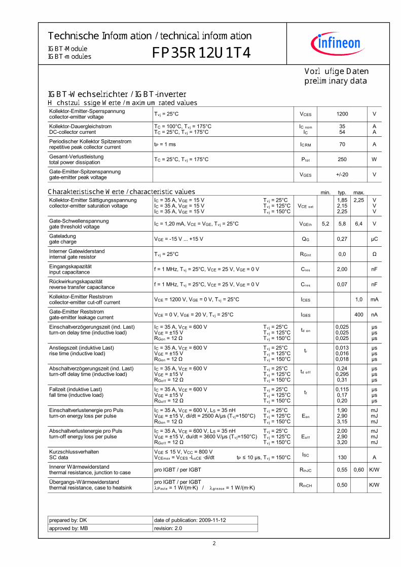
Ausgangskennlinie IGBT-Wechselr. (typisch)Ausgangskennlinie IGBT-Wechselr. (typisch)Ausgangskennlinie IGBT-Wechselr. (typisch)Ausgangskennlinie IGBT-Wechselr. (typisch)output characteristic IGBT-inverter (typical)output characteristic IGBT-inverter (typical)output characteristic IGBT-inverter (typical)output characteristic IGBT-inverter (typical)I† = f (V†Š)I† = f (V†Š)I† = f (V†Š)I† = f (V†Š)V•Š = 15 VV•Š = 15 VV•Š = 15 VV•Š = 15 V
V†Š [V]
I† [A]
0,0 0,5 1,0 1,5 2,0 2,5 3,0 3,5 4,00
5
10
15
20
25
30
35
40
45
50
55
60
65
70
TÝÎ = 25°CTÝÎ = 125°CTÝÎ = 150°C
Ausgangskennlinienfeld IGBT-Wechselr. (typisch)Ausgangskennlinienfeld IGBT-Wechselr. (typisch)Ausgangskennlinienfeld IGBT-Wechselr. (typisch)Ausgangskennlinienfeld IGBT-Wechselr. (typisch)output characteristic IGBT-inverter (typical)output characteristic IGBT-inverter (typical)output characteristic IGBT-inverter (typical)output characteristic IGBT-inverter (typical)I† = f (V†Š)I† = f (V†Š)I† = f (V†Š)I† = f (V†Š)TÝÎ = 150°CTÝÎ = 150°CTÝÎ = 150°CTÝÎ = 150°C
V†Š [V]
I† [A]
0,0 1,0 2,0 3,0 4,0 5,00
5
10
15
20
25
30
35
40
45
50
55
60
65
70
V•Š = 19VV•Š = 17VV•Š = 15VV•Š = 13VV•Š = 11VV•Š = 9V
Übertragungscharakteristik IGBT-Wechselr. (typisch)Übertragungscharakteristik IGBT-Wechselr. (typisch)Übertragungscharakteristik IGBT-Wechselr. (typisch)Übertragungscharakteristik IGBT-Wechselr. (typisch)transfer characteristic IGBT-inverter (typical)transfer characteristic IGBT-inverter (typical)transfer characteristic IGBT-inverter (typical)transfer characteristic IGBT-inverter (typical)I† = f (V•Š)I† = f (V•Š)I† = f (V•Š)I† = f (V•Š)V†Š = 20 VV†Š = 20 VV†Š = 20 VV†Š = 20 V
V•Š [V]
I† [A]
5 6 7 8 9 10 11 12 130
5
10
15
20
25
30
35
40
45
50
55
60
65
70
TÝÎ = 25°CTÝÎ = 125°CTÝÎ = 150°C
Schaltverluste IGBT-Wechselr. (typisch)Schaltverluste IGBT-Wechselr. (typisch)Schaltverluste IGBT-Wechselr. (typisch)Schaltverluste IGBT-Wechselr. (typisch)switching losses IGBT-inverter (typical)switching losses IGBT-inverter (typical)switching losses IGBT-inverter (typical)switching losses IGBT-inverter (typical)EÓÒ = f (I†), EÓËË = f (I†)EÓÒ = f (I†), EÓËË = f (I†)EÓÒ = f (I†), EÓËË = f (I†)EÓÒ = f (I†), EÓËË = f (I†)V•Š = ±15 V, R•ÓÒ = 12 Â, R•ÓËË = 12 Â, V†Š = 600 VV•Š = ±15 V, R•ÓÒ = 12 Â, R•ÓËË = 12 Â, V†Š = 600 VV•Š = ±15 V, R•ÓÒ = 12 Â, R•ÓËË = 12 Â, V†Š = 600 VV•Š = ±15 V, R•ÓÒ = 12 Â, R•ÓËË = 12 Â, V†Š = 600 V
I† [A]
E [mJ]
0 10 20 30 40 50 60 700,0
1,0
2,0
3,0
4,0
5,0
6,0
7,0
8,0
9,0
10,0
EÓÒ, TÝÎ = 125°CEÓËË, TÝÎ = 125°CEÓÒ, TÝÎ = 150°CEÓËË, TÝÎ = 150°C

8
Technische Information / technical information
FP35R12U1T4IGBT-ModuleIGBT-modules
prepared by: DK
approved by: MB
date of publication: 2009-11-12
revision: 2.0
Vorläufige Datenpreliminary data
Schaltverluste IGBT-Wechselr. (typisch)Schaltverluste IGBT-Wechselr. (typisch)Schaltverluste IGBT-Wechselr. (typisch)Schaltverluste IGBT-Wechselr. (typisch)switching losses IGBT-Inverter (typical)switching losses IGBT-Inverter (typical)switching losses IGBT-Inverter (typical)switching losses IGBT-Inverter (typical)EÓÒ = f (R•), EÓËË = f (R•)EÓÒ = f (R•), EÓËË = f (R•)EÓÒ = f (R•), EÓËË = f (R•)EÓÒ = f (R•), EÓËË = f (R•)V•Š = ±15 V, I† = 35 A, V†Š = 600 VV•Š = ±15 V, I† = 35 A, V†Š = 600 VV•Š = ±15 V, I† = 35 A, V†Š = 600 VV•Š = ±15 V, I† = 35 A, V†Š = 600 V
R• [Â]
E [mJ]
0 20 40 60 80 100 120 1400
2
4
6
8
10
12
14
EÓÒ, TÝÎ = 125°CEÓËË, TÝÎ = 125°CEÓÒ, TÝÎ = 150°CEÓËË, TÝÎ = 150°C
Transienter Wärmewiderstand IGBT-Wechselr.Transienter Wärmewiderstand IGBT-Wechselr.Transienter Wärmewiderstand IGBT-Wechselr.Transienter Wärmewiderstand IGBT-Wechselr.transient thermal impedance IGBT-invertertransient thermal impedance IGBT-invertertransient thermal impedance IGBT-invertertransient thermal impedance IGBT-inverterZÚÌœ™ = f (t)ZÚÌœ™ = f (t)ZÚÌœ™ = f (t)ZÚÌœ™ = f (t)
t [s]
ZÚÌœ™ [K/W]
0,001 0,01 0,1 1 100,01
0,1
1
10
ZÚÌœ™ : IGBT
i: rÍ[K/W]: Í[s]:
1 0,051 0,0005
2 0,118 0,005
3 0,412 0,05
4 0,469 0,2
τ
Sicherer Rückwärts-Arbeitsbereich IGBT-Wr. (RBSOA)Sicherer Rückwärts-Arbeitsbereich IGBT-Wr. (RBSOA)Sicherer Rückwärts-Arbeitsbereich IGBT-Wr. (RBSOA)Sicherer Rückwärts-Arbeitsbereich IGBT-Wr. (RBSOA)reverse bias safe operating area IGBT-inv. (RBSOA)reverse bias safe operating area IGBT-inv. (RBSOA)reverse bias safe operating area IGBT-inv. (RBSOA)reverse bias safe operating area IGBT-inv. (RBSOA)I† = f (V†Š)I† = f (V†Š)I† = f (V†Š)I† = f (V†Š)V•Š = ±15 V, R•ÓËË = 12 Â, TÝÎ = 150°CV•Š = ±15 V, R•ÓËË = 12 Â, TÝÎ = 150°CV•Š = ±15 V, R•ÓËË = 12 Â, TÝÎ = 150°CV•Š = ±15 V, R•ÓËË = 12 Â, TÝÎ = 150°C
V†Š [V]
I† [A]
0 200 400 600 800 1000 1200 14000
7
14
21
28
35
42
49
56
63
70
77
I†, ModulI†, Chip
Durchlasskennlinie der Diode-Wechselr. (typisch)Durchlasskennlinie der Diode-Wechselr. (typisch)Durchlasskennlinie der Diode-Wechselr. (typisch)Durchlasskennlinie der Diode-Wechselr. (typisch)forward characteristic of diode-inverter (typical)forward characteristic of diode-inverter (typical)forward characteristic of diode-inverter (typical)forward characteristic of diode-inverter (typical)IŒ = f (VŒ)IŒ = f (VŒ)IŒ = f (VŒ)IŒ = f (VŒ)
VΠ[V]
IΠ[A]
0,0 0,5 1,0 1,5 2,0 2,50
5
10
15
20
25
30
35
40
45
50
55
60
65
70
TÝÎ = 25°CTÝÎ = 125°CTÝÎ = 150°C
9
Technische Information / technical information
FP35R12U1T4IGBT-ModuleIGBT-modules
prepared by: DK
approved by: MB
date of publication: 2009-11-12
revision: 2.0
Vorläufige Datenpreliminary data
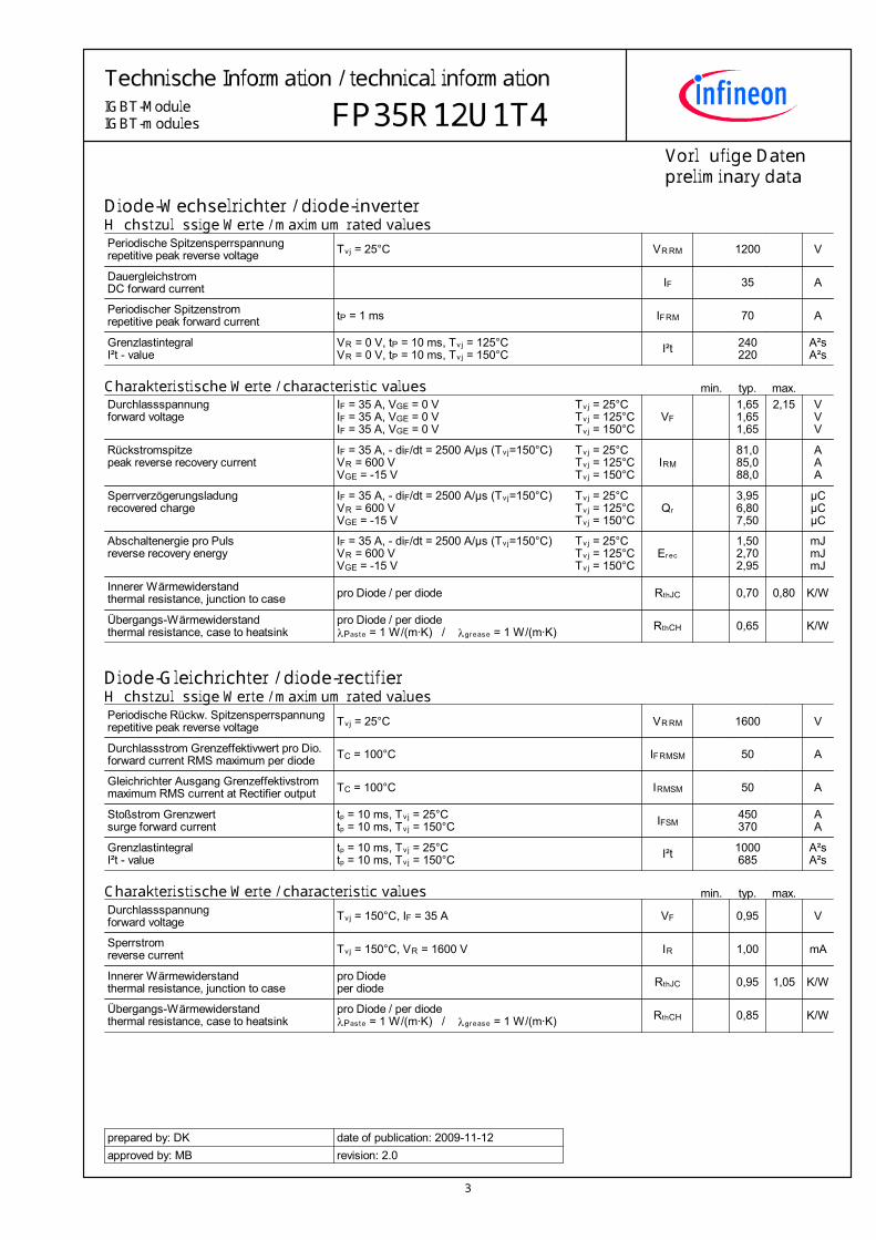
Schaltverluste Diode-Wechselr. (typisch)Schaltverluste Diode-Wechselr. (typisch)Schaltverluste Diode-Wechselr. (typisch)Schaltverluste Diode-Wechselr. (typisch)switching losses diode-inverter (typical)switching losses diode-inverter (typical)switching losses diode-inverter (typical)switching losses diode-inverter (typical)EØþÊ = f (IŒ)EØþÊ = f (IŒ)EØþÊ = f (IŒ)EØþÊ = f (IŒ)R•ÓÒ = 12 Â, V†Š = 600 VR•ÓÒ = 12 Â, V†Š = 600 VR•ÓÒ = 12 Â, V†Š = 600 VR•ÓÒ = 12 Â, V†Š = 600 V
IΠ[A]
E [mJ]
0 10 20 30 40 50 60 700,0
1,0
2,0
3,0
4,0
5,0
EØþÊ, TÝÎ = 125°CEØþÊ, TÝÎ = 150°C
Schaltverluste Diode-Wechselr. (typisch)Schaltverluste Diode-Wechselr. (typisch)Schaltverluste Diode-Wechselr. (typisch)Schaltverluste Diode-Wechselr. (typisch)switching losses diode-inverter (typical)switching losses diode-inverter (typical)switching losses diode-inverter (typical)switching losses diode-inverter (typical)EØþÊ = f (R•)EØþÊ = f (R•)EØþÊ = f (R•)EØþÊ = f (R•)IŒ = 35 A, V†Š = 600 VIŒ = 35 A, V†Š = 600 VIŒ = 35 A, V†Š = 600 VIŒ = 35 A, V†Š = 600 V
R• [Â]
E [mJ]
0 20 40 60 80 100 120 1400,0
0,5
1,0
1,5
2,0
2,5
3,0
3,5
4,0
EØþÊ, TÝÎ = 125°CEØþÊ, TÝÎ = 150°C
Transienter Wärmewiderstand Diode-Wechselr.Transienter Wärmewiderstand Diode-Wechselr.Transienter Wärmewiderstand Diode-Wechselr.Transienter Wärmewiderstand Diode-Wechselr.transient thermal impedance diode-invertertransient thermal impedance diode-invertertransient thermal impedance diode-invertertransient thermal impedance diode-inverterZÚÌœ™ = f (t)ZÚÌœ™ = f (t)ZÚÌœ™ = f (t)ZÚÌœ™ = f (t)
t [s]
ZÚÌœ™ [K/W]
0,001 0,01 0,1 1 100,1
1
10
ZÚÌœ™ : Diode
i: rÍ[K/W]: Í[s]:
1 0,09 0,0005
2 0,206 0,005
3 0,554 0,05
4 0,499 0,2
τ
Durchlasskennlinie der Diode-Gleichrichter (typisch)Durchlasskennlinie der Diode-Gleichrichter (typisch)Durchlasskennlinie der Diode-Gleichrichter (typisch)Durchlasskennlinie der Diode-Gleichrichter (typisch)forward characteristic of diode-rectifier (typical)forward characteristic of diode-rectifier (typical)forward characteristic of diode-rectifier (typical)forward characteristic of diode-rectifier (typical)IŒ = f (VŒ)IŒ = f (VŒ)IŒ = f (VŒ)IŒ = f (VŒ)
VΠ[V]
IΠ[A]
0,2 0,4 0,6 0,8 1,0 1,2 1,40
5
10
15
20
25
30
35
40
45
50
55
60
65
70
TÝÎ = 25°CTÝÎ = 150°C

10
Technische Information / technical information
FP35R12U1T4IGBT-ModuleIGBT-modules
prepared by: DK
approved by: MB
date of publication: 2009-11-12
revision: 2.0
Vorläufige Datenpreliminary data
Ausgangskennlinie IGBT-Brems-Copper (typisch)Ausgangskennlinie IGBT-Brems-Copper (typisch)Ausgangskennlinie IGBT-Brems-Copper (typisch)Ausgangskennlinie IGBT-Brems-Copper (typisch)output characteristic IGBT-brake-chopper (typical)output characteristic IGBT-brake-chopper (typical)output characteristic IGBT-brake-chopper (typical)output characteristic IGBT-brake-chopper (typical)I† = f (V†Š)I† = f (V†Š)I† = f (V†Š)I† = f (V†Š)V•Š = 15 VV•Š = 15 VV•Š = 15 VV•Š = 15 V
V†Š [V]
I† [A]
0,0 0,5 1,0 1,5 2,0 2,5 3,0 3,5 4,00
5
10
15
20
25
30
35
40
45
50
55
60
65
70
TÝÎ = 25°CTÝÎ = 125°CTÝÎ = 150°C
Durchlasskennlinie der Diode-Brems-Chopper (typisch)Durchlasskennlinie der Diode-Brems-Chopper (typisch)Durchlasskennlinie der Diode-Brems-Chopper (typisch)Durchlasskennlinie der Diode-Brems-Chopper (typisch)forward characteristic of diode-brake-chopper (typical)forward characteristic of diode-brake-chopper (typical)forward characteristic of diode-brake-chopper (typical)forward characteristic of diode-brake-chopper (typical)IŒ = f (VŒ)IŒ = f (VŒ)IŒ = f (VŒ)IŒ = f (VŒ)
VΠ[V]
IΠ[A]
0,0 0,5 1,0 1,5 2,0 2,50
2
4
6
8
10
12
14
16
18
20
TÝÎ = 25°CTÝÎ = 125°CTÝÎ = 150°C
NTC-Temperaturkennlinie (typisch)NTC-Temperaturkennlinie (typisch)NTC-Temperaturkennlinie (typisch)NTC-Temperaturkennlinie (typisch)NTC-temperature characteristic (typical)NTC-temperature characteristic (typical)NTC-temperature characteristic (typical)NTC-temperature characteristic (typical)R = f (T)R = f (T)R = f (T)R = f (T)
T† [°C]
R[Â]
0 20 40 60 80 100 120 140 160100
1000
10000
100000
RÚáÔ

11
Technische Information / technical information
FP35R12U1T4IGBT-ModuleIGBT-modules
prepared by: DK
approved by: MB
date of publication: 2009-11-12
revision: 2.0
Vorläufige Datenpreliminary data
Schaltplan / circuit diagram
ϑ
Gehäuseabmessungen / package outlines
Infineon
12
Technische Information / technical information
FP35R12U1T4IGBT-ModuleIGBT-modules
prepared by: DK
approved by: MB
date of publication: 2009-11-12
revision: 2.0
Vorläufige Datenpreliminary data
Nutzungsbedingungen
Die in diesem Produktdatenblatt enthaltenen Daten sind ausschließlich für technisch geschultes Fachpersonal bestimmt. Die Beurteilung der Eignung dieses Produktes für Ihre Anwendung sowie die Beurteilung der Vollständigkeit der bereitgestellten Produktdaten für diese Anwendung obliegt Ihnen bzw. Ihren technischen Abteilungen.
In diesem Produktdatenblatt werden diejenigen Merkmale beschrieben, für die wir eine liefervertragliche Gewährleistung übernehmen. Eine solche Gewährleistung richtet sich ausschließlich nach Maßgabe der im jeweiligen Liefervertrag enthaltenen Bestimmungen. Garantien jeglicher Art werden für das Produkt und dessen Eigenschaften keinesfalls übernommen.
Sollten Sie von uns Produktinformationen benötigen, die über den Inhalt dieses Produktdatenblatts hinausgehen und insbesondere eine spezifische Verwendung und den Einsatz dieses Produktes betreffen, setzen Sie sich bitte mit dem für Sie zuständigen Vertriebsbüro in Verbindung (siehe www.infineon.com, Vertrieb&Kontakt). Für Interessenten halten wir Application Notes bereit.
Aufgrund der technischen Anforderungen könnte unser Produkt gesundheitsgefährdende Substanzen enthalten. Bei Rückfragen zu den in diesem Produkt jeweils enthaltenen Substanzen setzen Sie sich bitte ebenfalls mit dem für Sie zuständigen Vertriebsbüro in Verbindung.
Sollten Sie beabsichtigen, das Produkt in Anwendungen der Luftfahrt, in gesundheits- oder lebensgefährdenden oder lebenserhaltenden Anwendungsbereichen einzusetzen, bitten wir um Mitteilung. Wir weisen darauf hin, dass wir für diese Fälle - die gemeinsame Durchführung eines Risiko- und Qualitätsassessments; - den Abschluss von speziellen Qualitätssicherungsvereinbarungen; - die gemeinsame Einführung von Maßnahmen zu einer laufenden Produktbeobachtung dringend empfehlen und gegebenenfalls die Belieferung von der Umsetzung solcher Maßnahmen abhängig machen.
Soweit erforderlich, bitten wir Sie, entsprechende Hinweise an Ihre Kunden zu geben.
Inhaltliche Änderungen dieses Produktdatenblatts bleiben vorbehalten.
Terms & Conditions of usage
The data contained in this product data sheet is exclusively intended for technically trained staff. You and your technical departments will have to evaluate the suitability of the product for the intended application and the completeness of the product data with respect to such application.
This product data sheet is describing the characteristics of this product for which a warranty is granted. Any such warranty is granted exclusively pursuant the terms and conditions of the supply agreement. There will be no guarantee of any kind for the product and its characteristics.
Should you require product information in excess of the data given in this product data sheet or which concerns the specific application of our product, please contact the sales office, which is responsible for you (see www.infineon.com, sales&contact). For those that are specifically interested we may provide application notes.
Due to technical requirements our product may contain dangerous substances. For information on the types in question please contact the sales office, which is responsible for you.
Should you intend to use the Product in aviation applications, in health or live endangering or life support applications, please notify. Please note, that for any such applications we urgently recommend - to perform joint Risk and Quality Assessments; - the conclusion of Quality Agreements; - to establish joint measures of an ongoing product survey, and that we may make delivery depended on the realization of any such measures.
If and to the extent necessary, please forward equivalent notices to your customers.
Changes of this product data sheet are reserved.

Mouser Electronics
Authorized Distributor
Click to View Pricing, Inventory, Delivery & Lifecycle Information: Infineon:
FP35R12U1T4