Embed Size (px)
Citation preview
Technical Services and SMT Knowhow Database of Nihon Superior
Wayne NG, NSJ
Mar 07, 2018
🔒CONFIDENTIALNIHON SUPERIOR CO,. LTD. R&D CENTER

Agenda
• Who are we?
• Who are our technical partners?
• What can we offer besides soldering
material?
• SMT knowhow
© Nihon Superior Co. Ltd. May 2017

Head Office: Osaka, Japan
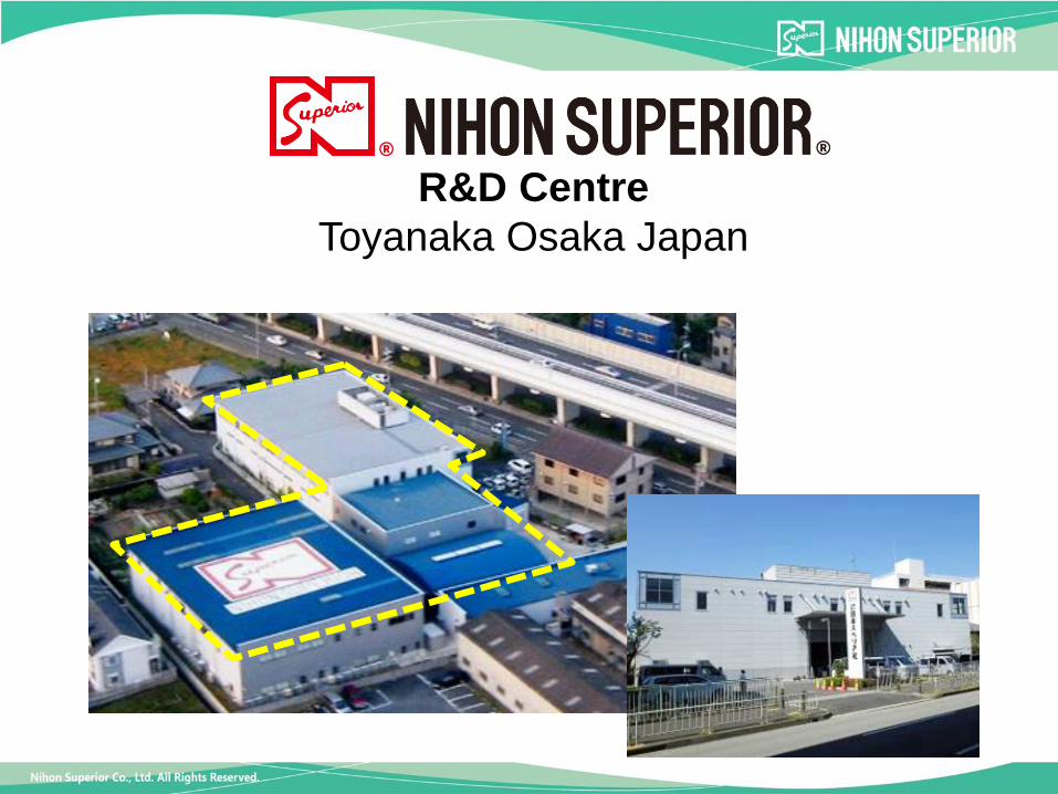
R&D Centre
Toyanaka Osaka Japan

Covering the Global Market
:Nihon Superior Grp.
:Global Partners
Nihon Superior Head Office
FCT Assembly
Nihon Superior
USA
Balver Zinn
DKL Metals
FCT AsiaNihon Superior Singapore
Nihon Superior Asia
Nihon Superior Thai
Nihon Superior Hong Kong
Nihon Superior Suzhou
Nihon Superior Shanghai
Nihon Superior Taiwan
Cobar
WKK
White Solder
Nihon Superior Indonesia
Nihon Superior Vietnam
Persang Alloy India
AIM Solder
NS Offices NS Licensees
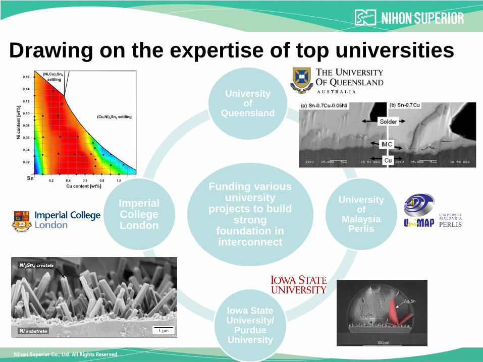
Funding various university
projects to build strong
foundation in interconnect
University of
Queensland
University of
Malaysia Perlis
Iowa State University/
Purdue University
Imperial College London
Drawing on the expertise of top universities

Memberships• IPC
• iNEMI (International Electronics Manufacturing Initiative)
• Universal’s Advanced Research in Electronics Assembly (AREA) Consortium
• HDP UG (High Density Packaging User Group)
• Soldertec
• Participant in JG-PP/JCAA Pb-Free Solder Project
• Participant in NASA/DoD Pb-Free Solder Project
• Surface Mount Technology Association International
• SIMTech Drop Impact Consortium
• Japan Welding Engineering Society Research
• Japan Welding Society Microjoining Commission
• Reliability Engineering Association of Japan
• Japan Institute of Electronics Packaging

Access to State of Art Analysis Facilities
Globally
SPring-8 is a synchrotron radiation facility located in Hyōgo Prefecture
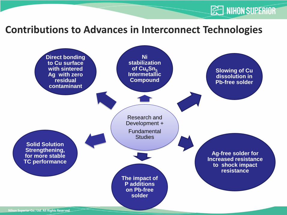
Contributions to Advances in Interconnect Technologies
Research and Development +
Fundamental Studies
Ni stabilization
of Cu6Sn5
Intermetallic Compound
Slowing of Cu dissolution in Pb-free solder
Ag-free solder for Increased resistance
to shock impact resistance
The impact of P additions on Pb-free
solder
Direct bonding to Cu surface with sintered Ag with zero
residual contaminant
Solid Solution Strengthening, for more stable TC performance

Slowing of Cu dissolution in Pb-free
solder
SN100C
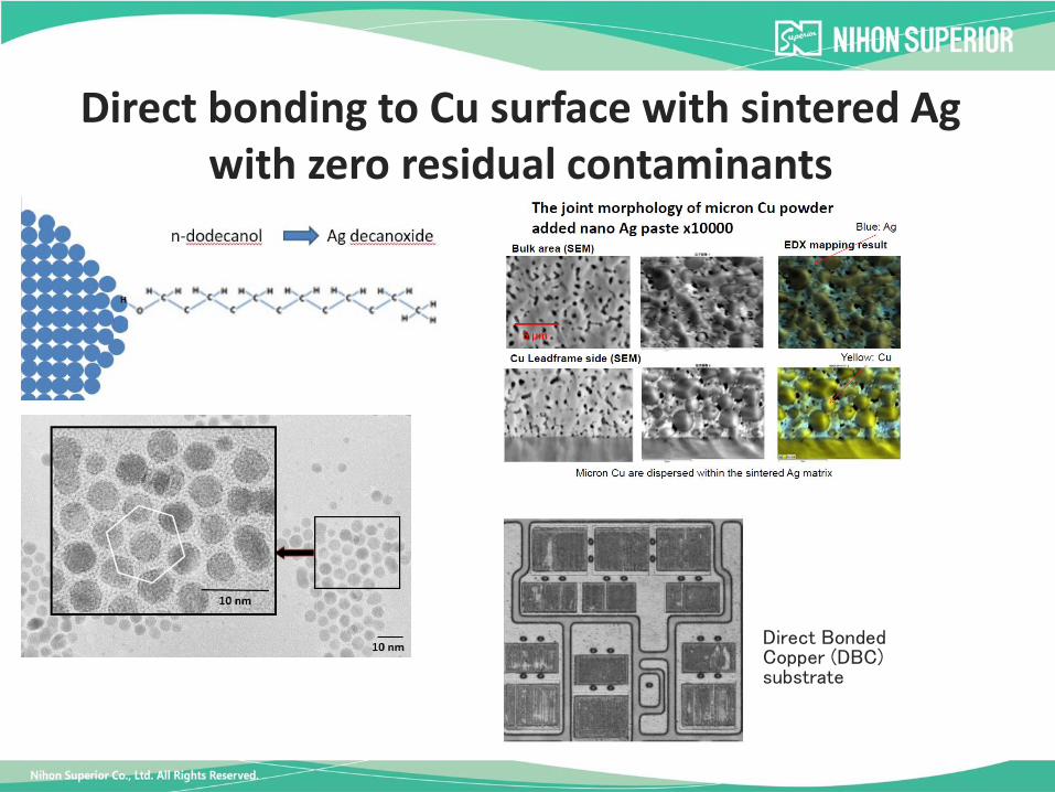
Direct bonding to Cu surface with sintered Ag with zero residual contaminants
Direct Bonded Copper (DBC) substrate

NSJ R&D
Toyanaka Osaka Japan
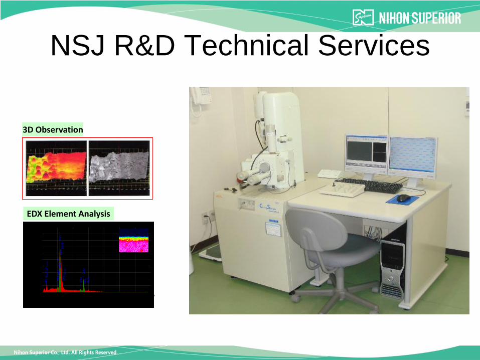
NSJ R&D Technical Services
0.00 3.00 6.00 9.00 12.00 15.00 18.00 21.00
keV
0
1000
2000
3000
4000
5000
6000
7000
8000
9000
10000
CPS
NiLl NiLa
NiKa
NiKb
CuLl CuLa
CuKa
CuKb
AgLaAgLbAgLb2SnLl
SnLa
SnLbSnLb2
SnLrSnLr2,
3D Observation
EDX Element Analysis
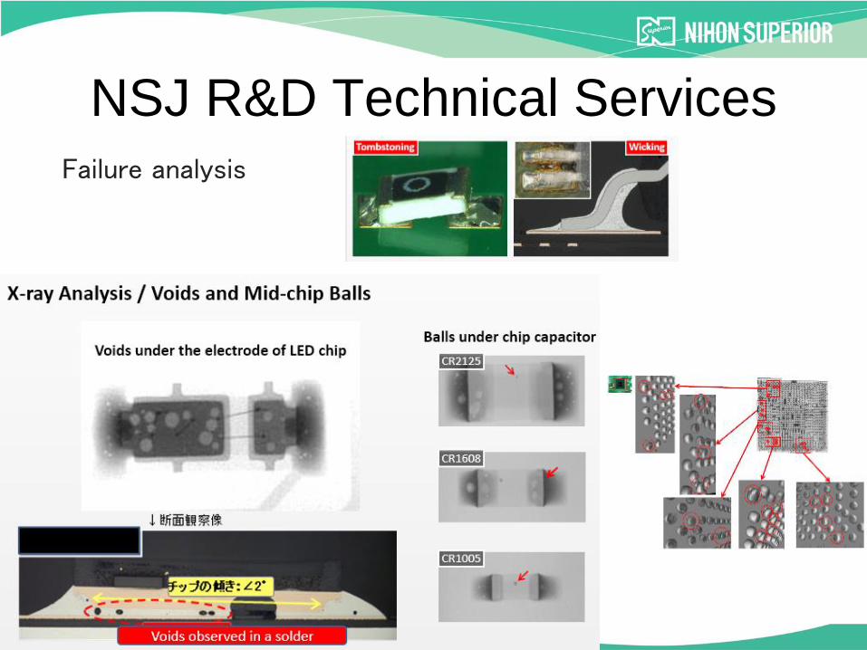
NSJ R&D Technical Services
Failure analysis

Diagnostic Testing Support for New Material Introduction
Support for Your Production
Digital MicroscopeSEMMicro focus X-ray Testing System
Wave-Soldering Machine
Selective Soldering Machine
Reflow Soldering Machine
X-Ray Fluorescence Spectrometer
Atomic Absorption Spectrometer
Optical Emission Spectrometer
ICP
15
Total Customer Support
Nihon Superior offers technical support for the introduction of new materials and optimization of lead-free soldering processes.

Wave-Soldering Machine
3 Zone PreheatCapable of achieving optimal
board preheat temperatures
Selective Soldering Machine
Wave Soldering Selective Soldering
Reflow Soldering
Reflow Soldering Machine
Good hole fill and fillet formation X-
Y motion makes it possible to
approach each joint from the
optimum direction
8 Heating Zones (5 Preheat
Zones, 3 Reflow Zones)
Height of
solder jet flow
Support for qualifying new materials
16
Total Customer Support

Environmental Reliability TestingEquipment for environmental and reliability testing
Environmental chambers for Surface Insulation Resistance and Electromigration Testing
Thermal Shock Chambers
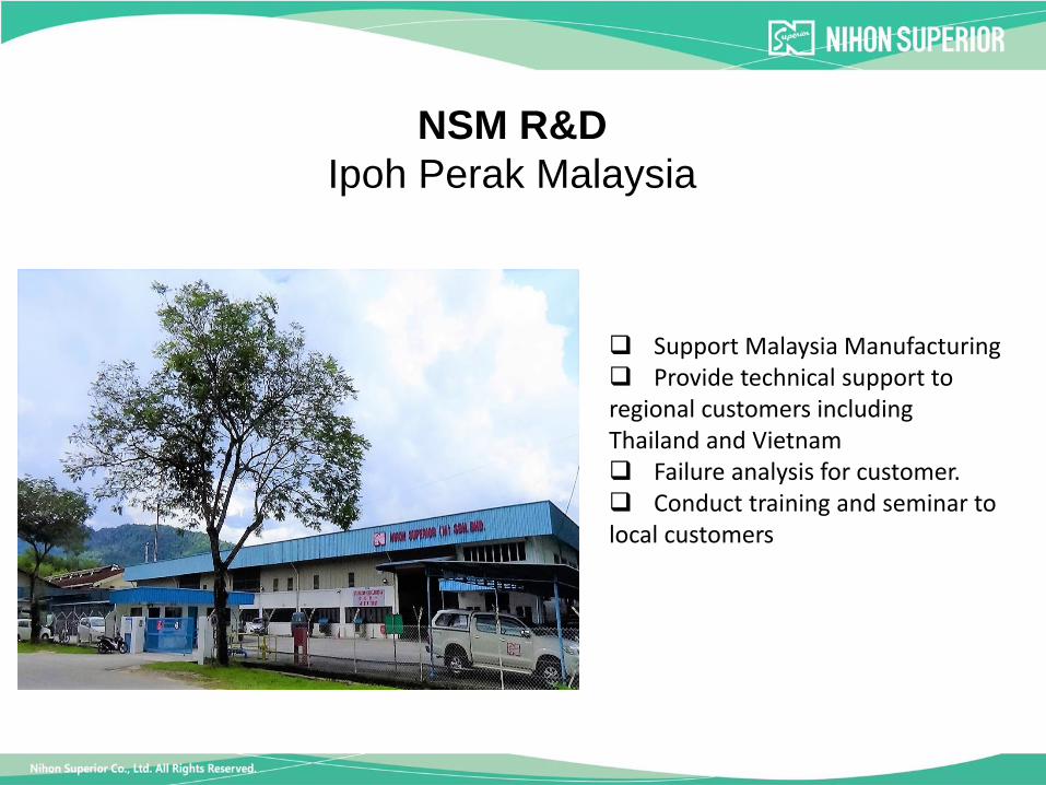
NSM R&D
Ipoh Perak Malaysia
Support Malaysia Manufacturing Provide technical support to regional customers including Thailand and Vietnam Failure analysis for customer. Conduct training and seminar to local customers

JEOL SEM/EDX
JEOL EDX
System
KEYENCE Digital Microscope
OLYMPUS Metallurgical
Microscope
Testing Facilities
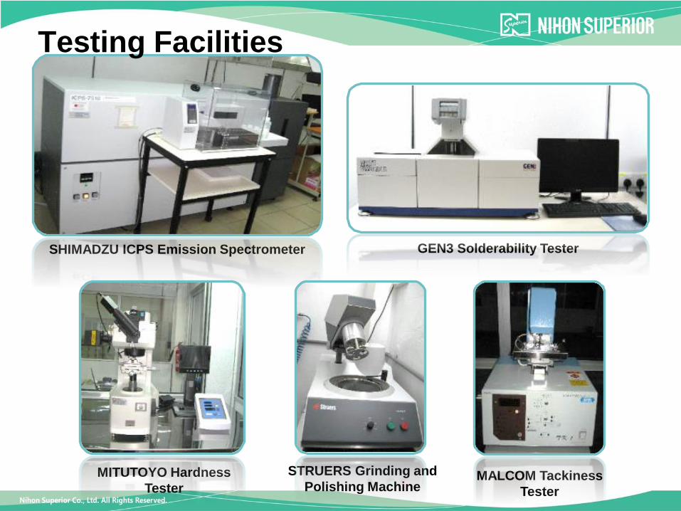
GEN3 Solderability TesterSHIMADZU ICPS Emission Spectrometer
MITUTOYO Hardness
Tester
STRUERS Grinding and
Polishing MachineMALCOM Tackiness
Tester
Testing Facilities

RIGAKU Differential
Scanning Calorimeter SHIMADZU Tensile Tester LABOCut
Testing Facilities

Vitronics Soltec Wave Soldering MachineDEK Printing Machine
Vitronics Soltec Reflow Oven
Testing Facilities

Digital Microscope
Failure AnalysisCross Section Analysis - Observation
SEM/EDX
POINT - 2
Surface observation
50X
Cross section sample
observation
A
B
Cross section sample
observationSurface observation
Point / Area analysis
Color Mapping analysis
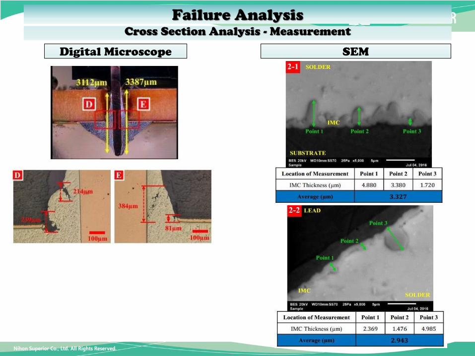
Digital Microscope
Failure AnalysisCross Section Analysis - Measurement
SEM

Failure AnalysisTensile Strength Test
Pull test
Elongation test
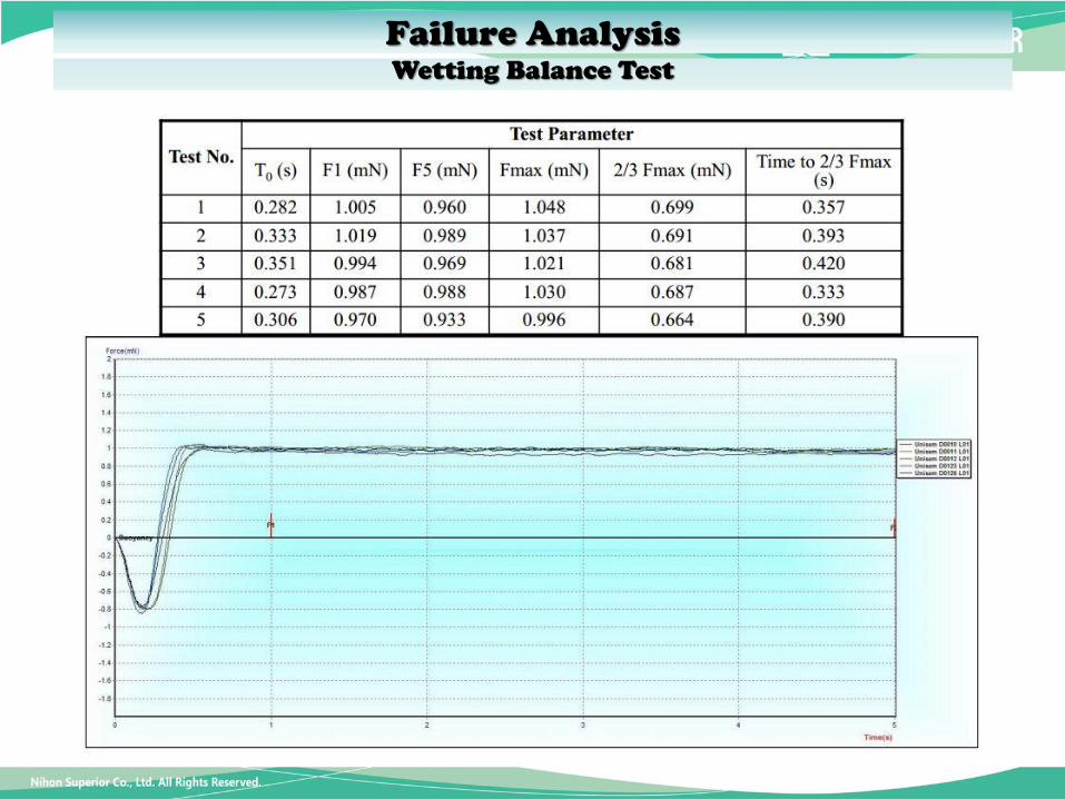
Failure AnalysisWetting Balance Test

●アメリカNIHON SUPERIOR USA, LLC1395 Hawk Island Dr Osage Beach, MO, 65065, U.S.A.TEL: +1-573-280-2357FAX: +1-619-923-2714
●台湾NIHON SUPERIOR (TAIWAN) CO.,LTD.4F., No.1, Sec.2, Dasing West Rd., Taoyuan City, Taoyuan 33046, Taiwan R.O.C.TEL: +886-(0)3-215-1119FAX: +886-(0)3-215-1335
●中国NIHON SUPERIOR (SHANGHAI) CO., LTD.29 Floor-H, Shang-Shi Building, No.18 Caoxibei Road, Xuhui District,Shanghai, 200030 ChinaTEL: +86-(0)21-6427-0038FAX: +86-(0)21-6441-0554NIHON SUPERIOR (SHANGHAI) CO., LTD. DONGGUAN BRANCH8-B Xingye Building, 89 Lianfeng Road, Chang'an, Dongguan, Guangdong, 523850 ChinaTEL: +86-(0)769-82750225FAX: +86-(0)769-82750226NIHON SUPERIOR (SUZHOU) CO., LTD.Loufeng Under Taking Development Square No.11 Yanghe Road, Suzhou Industrial Park,215122 ChinaTEL: +86-(0)512-6748-8352FAX: +86-(0)512-6748-8551
●ベトナムREPRESENTATIVE OF NIHON SUPERIOR (THAILAND) CO., LTD. IN HANOIHoa Binh International Towers, 11th Floor 106 Hoang Quoc Viet StreetNghia Do ward Cau Giay District, Hanoi City, VietnamTEL: +84-4-3-7689755FAX: +84-4-3-7689757
●タイNIHON SUPERIOR (THAILAND) CO., LTD.13th Floor Unit G, 216/56 L.P.N. Tower, Nanglinchee Rd, Chong Non See, Yannawa,Bangkok, 10120 ThailandTEL: +66-(0)2-285-4471FAX: +66-(0)2-285-4358
●インドネシアNIHON SUPERIOR (SINGAPORE) PTE. LTD.INDONESIA REPRESENTATIVE OFFICEWisma 46-Kota BNI, #48-04 Jl. Jendral Sudirman Kav.1, Jakarta 10220 -IndonesiaTEL: +62-815-8416-3010
●シンガポールNIHON SUPERIOR (SINGAPORE) PTE. LTD.5 Harper Road #04-03, Singapore 369673TEL: +65-6741-4633FAX: +65-6741-6636
●マレーシアNIHON SUPERIOR (M) SDN. BHD.Lot17, Jalan, Industri 1, Free Industrial Zone, Jelapang II, 30020 Ipoh, Perak, MalaysiaTEL: +60-(0)5-527-3792FAX: +60-(0)5-527-3659NIHON SUPERIOR ASIA SDN. BHD.Unit No.5, Level 13A, Block 5, MenaraVSQ@ PJ City Centre, JalanUtara, 46200 PetalingJaya, Selangor, MalaysiaTEL: +60-(0)3-7932-5875FAX: +60-(0)3-7931-5892
●本社(大阪)〒564-0063 大阪府吹田市江坂町1-16-15(NSビル)TEL:06-6380-1121(代表)FAX:06-6380-1262●東京営業所〒135-0042 東京都江東区木場2-7-15 第一びる別館4FTEL:03-3642-5234(代表)FAX:03-3642-5257●名古屋営業所〒466-0059 名古屋市昭和区福江2-5-4-802TEL:052-882-6011FAX:052-871-2434○津山工場〒708-1215 岡山県津山市杉宮778-1TEL:0868-29-3240FAX:0868-29-2242○豊中工場〒561-0894 大阪府豊中市勝部1-9-21TEL:06-6843-7591FAX:06-6853-7204○大阪物流センター〒561-0894 大阪府豊中市勝部1-9-21TEL:06-6843-7591FAX:06-6853-7204○R&Dセンター〒561-0894 大阪府豊中市勝部1-9-15TEL:06-6843-7155FAX:06-6843-7733
27
Your Local Contact

Agenda
• Who are we?
• Who are our technical partners?
• What can we offer besides material?
• SMT knowhow
© Nihon Superior Co. Ltd. May 2017

Through-hole component- Wave soldering- Selective soldering- Manual soldering
Surface mount technology, SMT component- SMT Reflow Soldering- Wave soldering, (certain limitations.
not applicable to fine pitch component)
https://learn.sparkfun.com/tutorials/integrated-circuits/ic-packages

SMT Process
© Nihon Superior Co. Ltd. May 2017
All the processes that control the formation of solder joints such as solder paste printing, reflow soldering, wave soldering, selective soldering, hand solder etc. control a significant majority of the opportunities for a defect

Surface Finishes to Protect Cu Pad
© Nihon Superior Co. Ltd. May 2017
• Cu is highly vulnerable to oxidation. Need surface protection to preserve the solderable surfaces as the PCB moves from PCB house to assembly
• Most common surface finishes:– Cu OSP (organic solderability preservative)
– ENIG (electroless nickel immersion gold)
– HASL (hot air solder leveling, SnPb or SN100C)
– ImAg (immersion silver)
– ImSn (immersion tin)
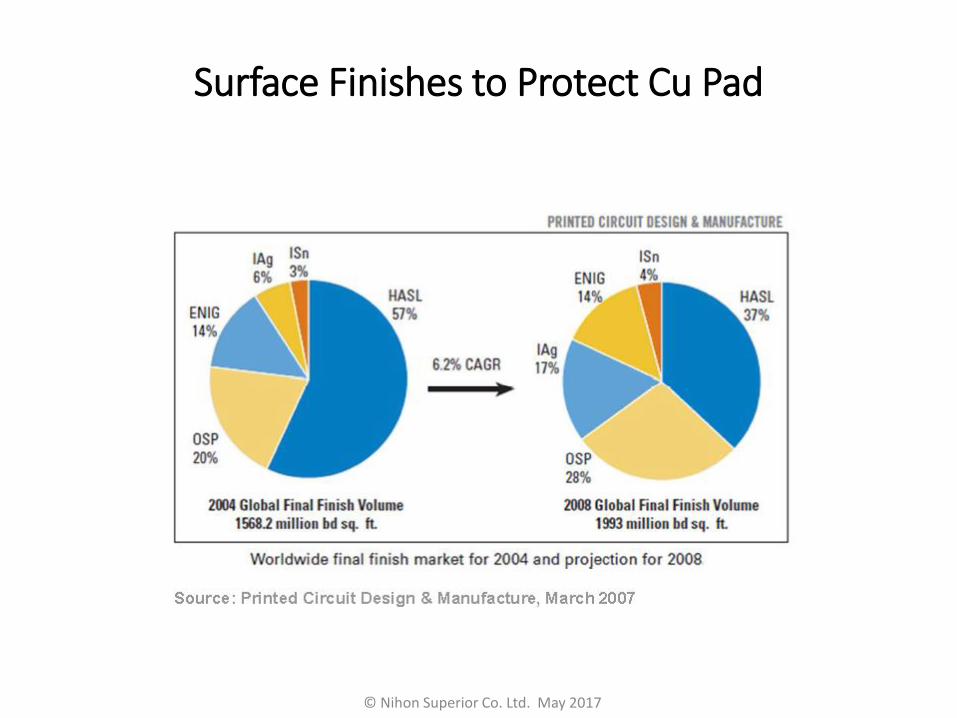
Surface Finishes to Protect Cu Pad
© Nihon Superior Co. Ltd. May 2017

What is HASL
© Nihon Superior Co. Ltd. May 2017
Solder Bath
Hot Air Knives
Pre-etched and Fluxed PCB
• HASL = Hot Air Solder Leveling
• HASL machine can be vertical or horizontal
260 -265°C

Cu OSP, ENIG, Im Ag, Im Sn
© Nihon Superior Co. Ltd. May 2017
Cu OSP ENIG
Im Ag Im Sn

Solder Paste Deposition
© Nihon Superior Co. Ltd. May 2017

Printing Process is Critical
• The formation of solder joints:• Solder paste printing
• Component placement
• Solder – reflow process
• A case study revealed that the solder paste printing process controlled in excess 80% of the opportunities for a defect
• There are many factor that influence the performance of the solder paste printing process

This is what we/your manager expects to see, IDEAL case
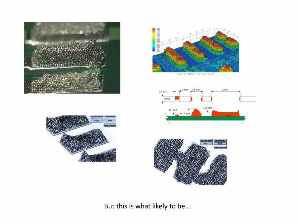
But this is what likely to be…
paste
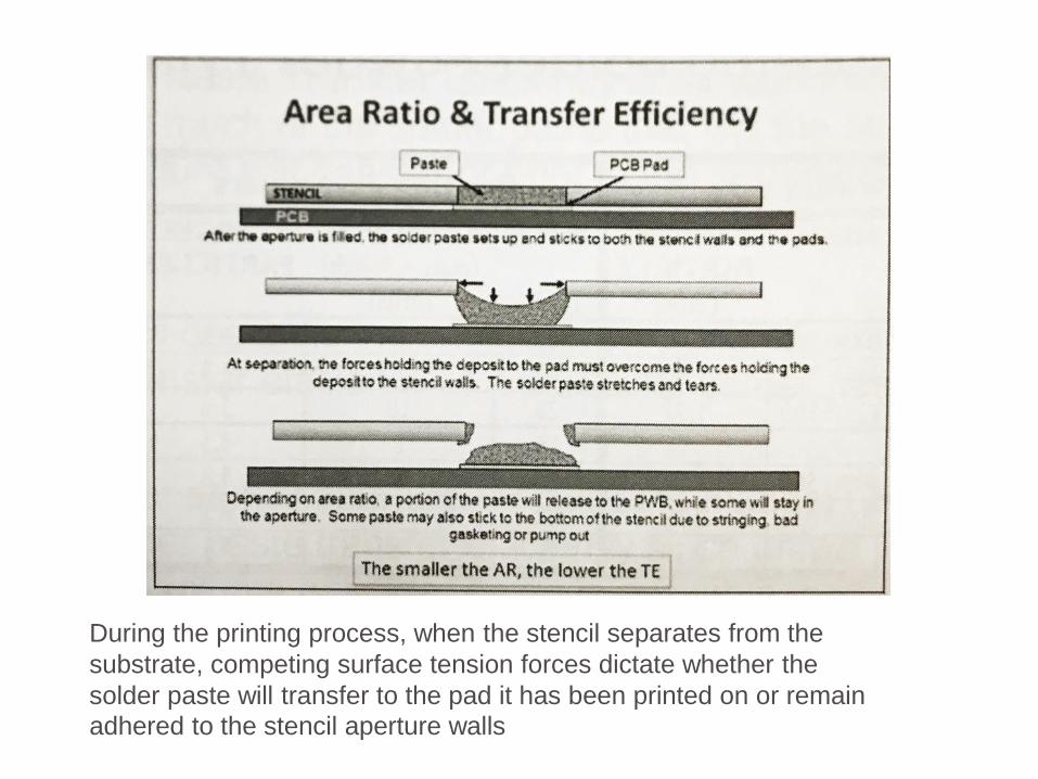
During the printing process, when the stencil separates from the
substrate, competing surface tension forces dictate whether the
solder paste will transfer to the pad it has been printed on or remain
adhered to the stencil aperture walls

Stencil Design
© Nihon Superior Co. Ltd. May 2017
• IPC-7525B—Stencil Design Guidelines
• Stencil thickness ranging from 100-150 µm
• Aspect Ratio = Width of Aperture Opening/Stencil Foil Thickness = W/T, must be greater than 1.5
• Area Ratio = Area of Aperture Opening/Area of Aperture Walls = W × L / 2 × (L+W) × T, must be greater than 0.66
• Aspect ratio relates to stencil manufacturing and area ratio relates to paste release


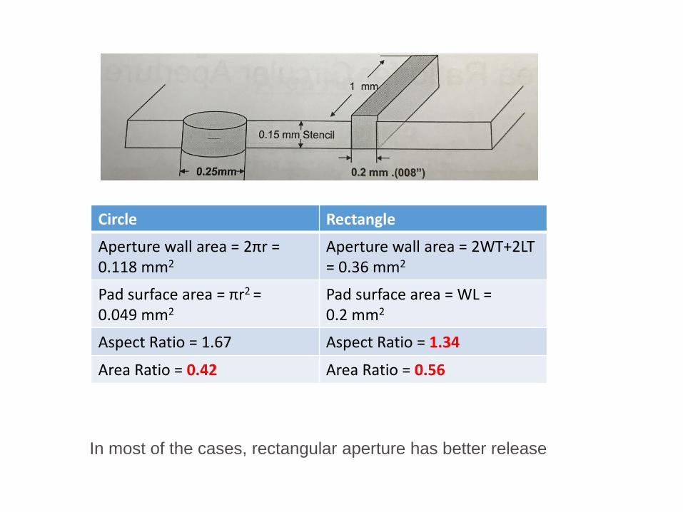
Circle Rectangle
Aperture wall area = 2πr = 0.118 mm2
Aperture wall area = 2WT+2LT = 0.36 mm2
Pad surface area = πr2 = 0.049 mm2
Pad surface area = WL = 0.2 mm2
Aspect Ratio = 1.67 Aspect Ratio = 1.34
Area Ratio = 0.42 Area Ratio = 0.56
In most of the cases, rectangular aperture has better release


Nano Coating Helps Paste Transfer and Print Definition
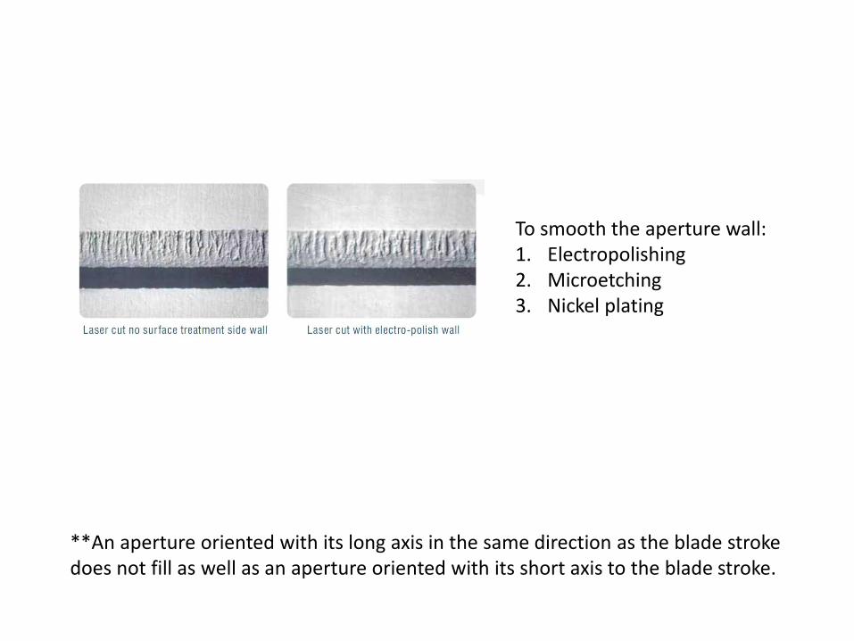
To smooth the aperture wall:1. Electropolishing2. Microetching3. Nickel plating
**An aperture oriented with its long axis in the same direction as the blade stroke does not fill as well as an aperture oriented with its short axis to the blade stroke.
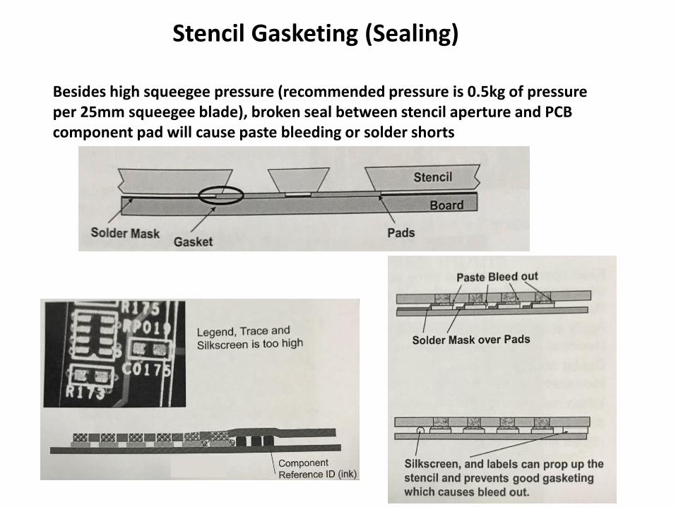
Stencil Gasketing (Sealing)
Besides high squeegee pressure (recommended pressure is 0.5kg of pressure per 25mm squeegee blade), broken seal between stencil aperture and PCB component pad will cause paste bleeding or solder shorts
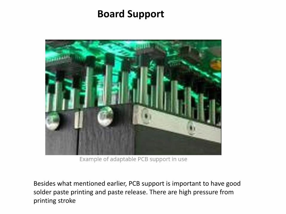
Besides what mentioned earlier, PCB support is important to have good solder paste printing and paste release. There are high pressure from printing stroke
Board Support
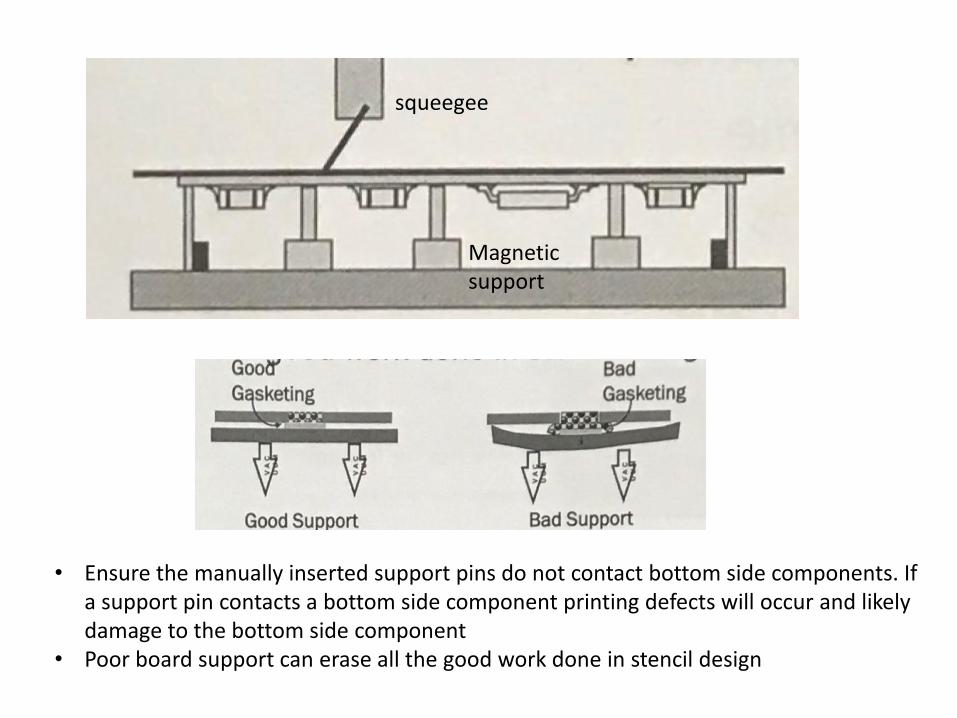
• Ensure the manually inserted support pins do not contact bottom side components. If a support pin contacts a bottom side component printing defects will occur and likely damage to the bottom side component
• Poor board support can erase all the good work done in stencil design
squeegee
Magnetic support

Board Stencil Separation Speed
• The separation of board from stencil needs to be controlled• Time should be sufficient to allow paste deposit clears the aperture then faster
separation speed, slow snap off• This is why good printer should have allowed 2 speed controls for this process

Amount of Paste on Stencil
• When the diameter of rolling paste smaller than 10mm, the transfer efficiency drops significantly.
• Recommended diameter is 10-15mm• It is important to replenish the paste regularly
0%
20%
40%
60%
80%
100%
120%
0 5 10 15 20 25 30
Tra
nsf
er
Eff
icie
ncy (
%)
Diameter of rolling paste:(mm)

General Guideline in Printing ParametersItem 推奨値/Recommend Tolerance or other options
Type of Stencil Laser (Stainless)Additive , Etching, Electroform, coated
with nano material
Squeeze material Metal Urethane
Squeeze angle ∠60° ∠45°-∠60°
Printing speed 50mm/sec 20-100mm/sec
Printing pressure20g/mm
(For example, a 300mm blade needs 6.0kg)10-30g/mm
Separation speed 1.0mm/sec 0.5-2.0mm/sec
Ambient environmentTemperature:25℃Humidity:40%RH
Temperature:±3℃Humidity:±20%RH
Delta temperature of paste on stencil ±1℃ ±2℃
Diameter of rolling paste Φ15mm φ10-20mm
Aspect ratio of stencil aperture 0.6以上 0.5以上
Printing speed has been tested in range of 2-150mm/s. The increase of printing speed will reduce the printability of paste. It is necessary to increase the printing pressure for high speed of printing. However, high pressure will increase the stress on stencil and squeegee. A balance needs to be maintained in printing speed and pressure
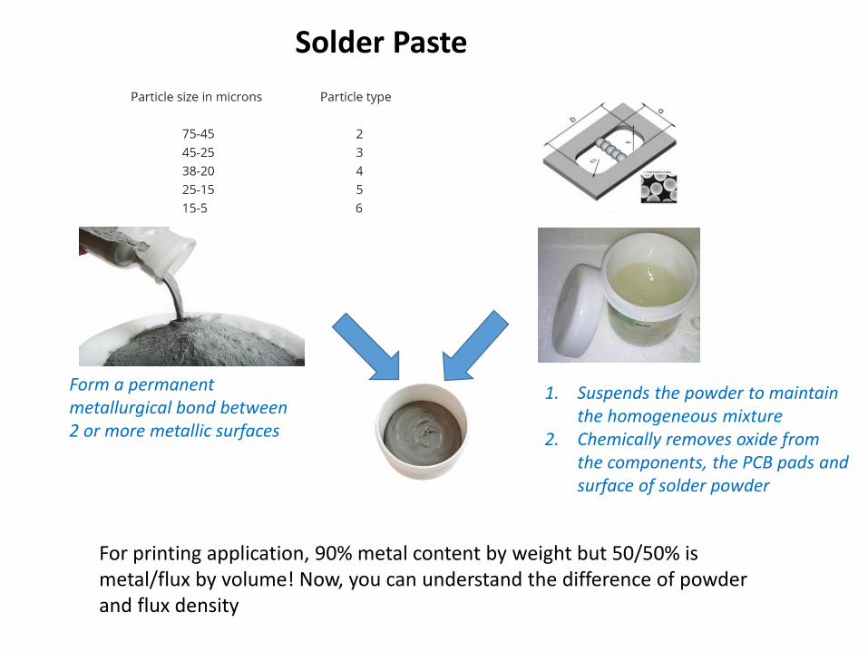
For printing application, 90% metal content by weight but 50/50% is metal/flux by volume! Now, you can understand the difference of powder and flux density
Form a permanent metallurgical bond between 2 or more metallic surfaces
1. Suspends the powder to maintain the homogeneous mixture
2. Chemically removes oxide from the components, the PCB pads and surface of solder powder
Solder Paste

Solder Paste Handling Guideline• Please keep this paste in refrigerator(at 0-10degC).
• Please do not open the container before the contents reach room temperature to avoid condensation of moisture on the paste.
• Please use by room temperature.
• Please do not mix solder paste from the stencil with unused paste in the jar
• Please mix at 1-2minutes to take care so as to prevent bubbles.
*Solder paste mixer condition:1minute at 1000rpm.
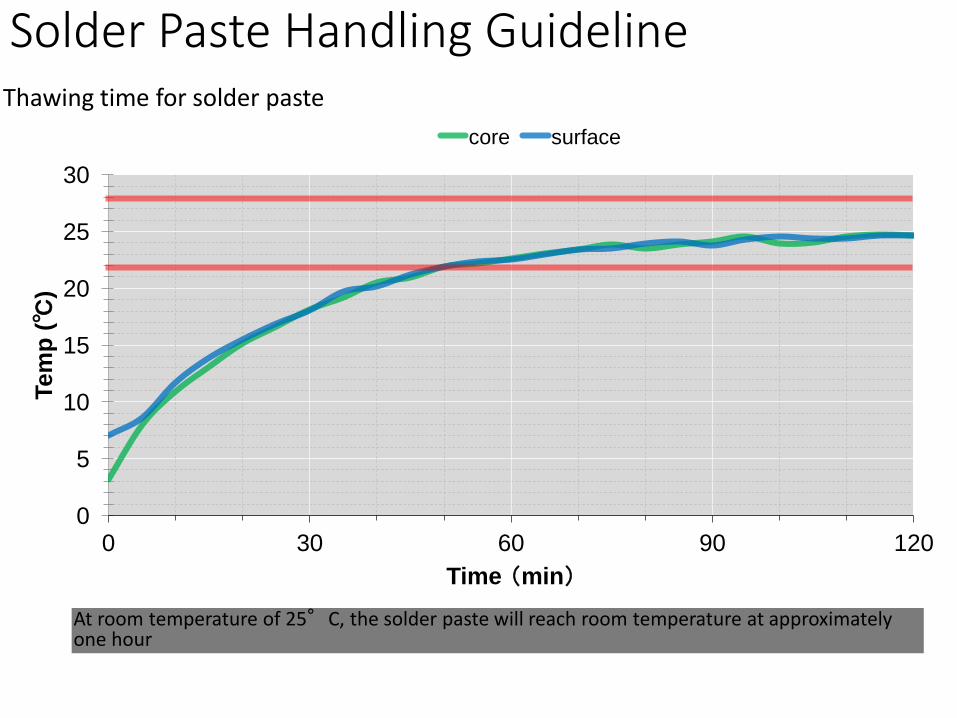
Solder Paste Handling Guideline
0
5
10
15
20
25
30
0 30 60 90 120
Tem
p (
℃)
Time (min)
core surface
At room temperature of 25°C, the solder paste will reach room temperature at approximately one hour
Thawing time for solder paste

Solder Paste Handling GuidelineCentrifugal spinning can warm the paste faster:
0
5
10
15
20
25
30
0 1 2 3 4 5 6 7 8 9 10
Tem
p(℃
)
Mixing time(min)
Spinning condition: 1000rpm with 500g jar
Paste temperature will reach room temperature with 1000rpm spinning for 7-8 minutes.

Solder Paste Handling GuidelineBut don’t warm or spin the paste too much!
0
100
200
300
400
500
600
10 15 20 25 30 35
粘度
Vis
cosity(P
a.s
)
温度 Temp(℃)
Shear Force-Temp-Viscosity Relationship
10rpm
3rpm
30rpm
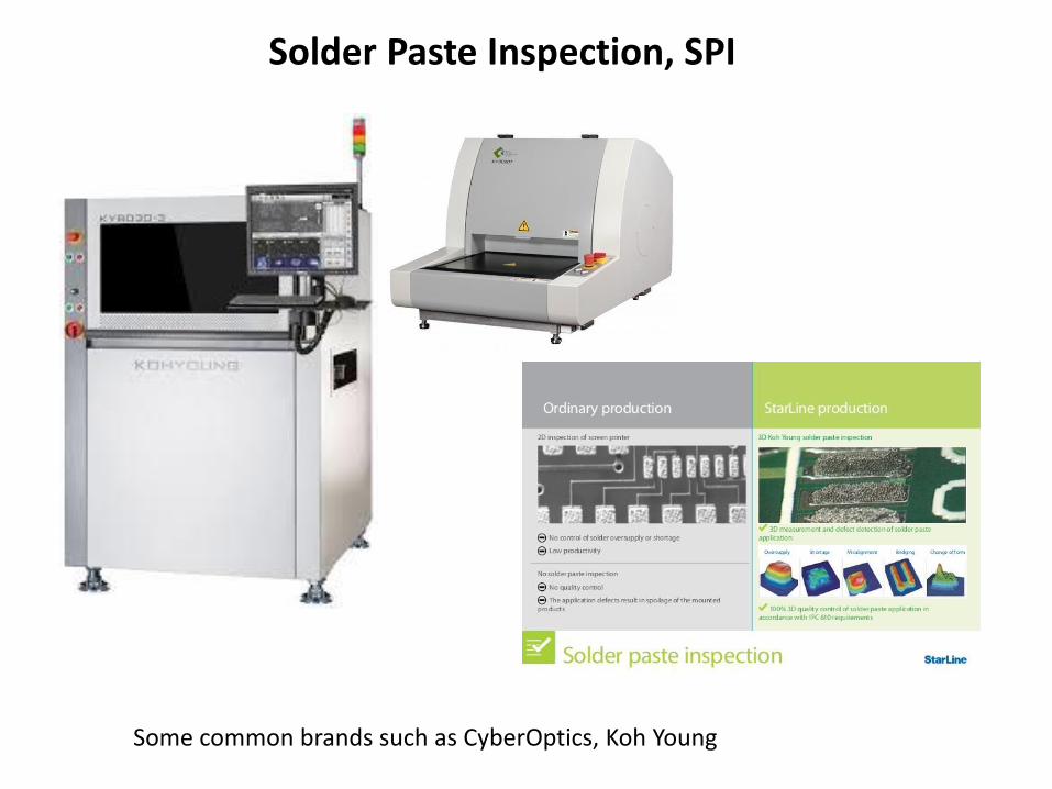
Solder Paste Inspection, SPI
Some common brands such as CyberOptics, Koh Young

Component Placement
Some familiar names such as ASM, Assembleon, Europlacer, Fuji, Hitachi, Juki, Mirae, Mydata, Panasonic, Samsung, Universal, Yamaha and others

Reflow Soldering Process
This is only recommendation of solder paste supplier. This is not a specification. But the limit of preheat or soaking (temperature, duration and ramp rate) needs to be followed strictly to keep the activity of flux till end of reflow process

Warpage of PCB and SMT component
Uncontrolled PCB and component warpage leads to Print and SMT defects and eventually a reliability concern!

Conclusion
© Nihon Superior Co. Ltd. May 2017
• No single factor which is responsible for a defect
• Any step/process during the SMT can be part of the root cause
• Need to have full understanding the steps in SMT in order to have
continuous improvement
• Due to rigidity of SMT component and small solder volume, solder
joint reliability is a crucial topic for this process