Embed Size (px)
Citation preview
i
SDM7540 Data Acquisition Driver Manual for Windows 98/2000/XP and DOS Version 1.0.x User’s Manual
SWM-640010024
Rev. A

RTD Embedded Technologies, INC. 103 Innovation Blvd.
State College, PA 16803-0906
Phone: +1-814-234-8087 FAX: +1-814-234-5218
[email protected] [email protected]
web site
http://www.rtd.com
iii
Revision History
05/04/2005 Initial Release
SDM7540 Data Acquisition Driver Manual for Windows 98/2000/XP and DOS Published by:
RTD Embedded Technologies, Inc.
103 Innovation Blvd. State College, PA 16803-0906
Copyright 2004 RTD Embedded Technologies, Inc.
All rights reserved Printed in U.S.A.
The RTD Logo is a registered trademark of RTD Embedded Technologies. cpuModule and utilityModule are trademarks of RTD Embedded Technologies. PS/2, PC/XT, PC/AT and IBM are trademarks of International Business Machines Inc. MS-DOS, Windows, Windows 95, Windows 98, Windows 2000 and Windows XP are trademarks of Microsoft Corp. PC/104 is a registered trademark of PC/104 Consortium. All other trademarks appearing in this doc-ument are the property of their respective owners.
Table of Contents
TABLE OF CONTENTS ....................................................................................................... IV
INTRODUCTION .................................................................................................................. 11
NOTATIONAL CONVENTIONS......................................................................................... 11
INSTALLATION.................................................................................................................... 11 INSTALLATION OF THE DRIVER AND EXAMPLE PROGRAMS IN WINDOWS................................... 11 INSTALLATION OF THE DRIVER AND EXAMPLE PROGRAMS IN DOS........................................... 13 THE SDM7540 BOARD DRIVER ................................................................................................ 13 INSTALLING A SECOND BOARD IN THE SYSTEM UNDER WINDOWS.............................................. 13 WORKING WITH OTHER BOARDS USING THE WINRT DRIVER ................................................... 13 THE DRIVER API FUNCTIONS .................................................................................................... 14 USING THE DRIVER WITHOUT THE WINDOWS GUI..................................................................... 14 REGISTRY SETTINGS IN WINDOWS.............................................................................................. 15 SDM7540 FEATURES ........................................................................................................... 17 MEASUREMENT SCENARIOS ...................................................................................................... 17 CHANNEL-GAIN CIRCUITRY....................................................................................................... 18 INTERRUPTS............................................................................................................................... 20 PRE AND POST TRIGGERING....................................................................................................... 22 ADVANCED DIGITAL TRIGGER ................................................................................................... 25 SYNCHRON BUS......................................................................................................................... 25 DATA TRANSFER WITH DMA..................................................................................................... 26 DRIVER API FUNCTION GROUPS ................................................................................... 29 DRIVER INITIALIZATION FUNCTIONS .......................................................................................... 29 GENERAL BOARD CONTROL FUNCTIONS ................................................................................... 29 FIFO MANIPULATION ................................................................................................................ 29 A/D CONVERTER ....................................................................................................................... 29 CHANNEL-GAIN TABLE MANIPULATION .................................................................................... 29 PACER CLOCK HANDLING.......................................................................................................... 30 BURST CLOCK HANDLING.......................................................................................................... 30 DELAY COUNTER FUNCTIONS.................................................................................................... 30 ABOUT COUNTER FUNCTIONS ................................................................................................... 30 SAMPLE COUNTER FUNCTIONS .................................................................................................. 30 D/A CONVERTER ....................................................................................................................... 30 DIGITAL I/O FUNCTIONS ............................................................................................................ 31 HIGH-SPEED DIGITAL INPUT FUNCTIONS ................................................................................... 31 USER INPUT/OUTPUT FUNCTIONS .............................................................................................. 31 USER TIMER-COUNTER FUNCTIONS........................................................................................... 32 INTERRUPT HANDLING............................................................................................................... 32 SYNCHRON BUS CONFIGURATION FUNCTIONS........................................................................... 32 EXTERNAL TRIGGER CONFIGURATION FUNCTIONS .................................................................... 32 DMA FUNCTIONS ...................................................................................................................... 32 MCBSP PORT CONTROL FUNCTIONS ......................................................................................... 33 CALIBRATION AND DSP CONTROL FUNCTIONS ......................................................................... 33
v
ALPHABETICAL DRIVER API FUNCTIONS REFERENCE .........................................34 NOTE ABOUT THE FUNCTION DEFINITIONS ..................................................................................34 A................................................................................................................................................34 ABORTDMA07540 ABORTDMA17540 .....................................................................................34 C................................................................................................................................................35 CLEARADFIFO7540..................................................................................................................35 CLEARALLIO7540 .....................................................................................................................35 CLEARCGT7540 ........................................................................................................................35 CLEARDAC1FIFO7540 CLEARDAC2FIFO7540.......................................................................36 CLEARDINFIFO7540...................................................................................................................36 CLEARDIO7540 .........................................................................................................................36 CLEARDIO0IRQSTATUS7540.....................................................................................................37 CLEARITMASK7540 ..................................................................................................................37 CLEARITOVERRUN7540 ............................................................................................................38 CLOSEBOARD7540.....................................................................................................................38 D................................................................................................................................................39 DACCLOCKFREERUN7540 ........................................................................................................39 DACCLOCKSTARTSELECT7540 .................................................................................................39 DACCLOCKSTOPSELECT7540 ...................................................................................................39 DEINSTALLDMA7540................................................................................................................40 E ................................................................................................................................................41 ENABLEACNTSTOP7540.............................................................................................................41 ENABLECGT7540 ......................................................................................................................41 ENABLECGTDIGITAL7540 .........................................................................................................41 ENABLECGTPAUSE7540 ...........................................................................................................42 ENABLEDIO0IRQ7540 ...............................................................................................................42 ENABLESBUS07540 ENABLESBUS17540 ENABLESBUS27540 ...................................................43 ERASEINTERNALFLASH7540 ......................................................................................................43 G................................................................................................................................................44 GET8254COUNT7540.................................................................................................................44 GET8254MODE7540 ..................................................................................................................44 GET8254STATUS7540................................................................................................................45 GETATTENTION7540..................................................................................................................45 GETACNTCOUNT7540................................................................................................................46 GETADCNTCOUNT7540 .............................................................................................................46 GETAUTOCALVERSION7540 ......................................................................................................46 GETBOARDTEMP7540 ...............................................................................................................47 GETBOOTLDRVERSION7540......................................................................................................47 GETDACDIVISOR7540...............................................................................................................47 GETDIO0CLOCK7540................................................................................................................48 GETDIO0COMPAREMODE7540 .................................................................................................48 GETDIO0COMPAREVALUE7540 ................................................................................................48 GETDIO0DIRECTION7540..........................................................................................................49 GETDIO0MASK7540 .................................................................................................................49 GETDIO1DIRECTION7540..........................................................................................................49 GETDIOSTATUS7540.................................................................................................................50 GETDMA0STATUS7540 GETDMA1STATUS7540......................................................................50 GETDMADONECHANNEL7540 ..................................................................................................51 GETDSPRESULTCODE7540 .......................................................................................................51
GETERRORSTATUS7540 ............................................................................................................ 51 GETFIFOSTATUS7540 ................................................................................................................ 52 GETITSTATUS7540 ................................................................................................................... 52 GETTIMERSTATUS7540............................................................................................................. 53 I................................................................................................................................................. 54 INITBOARD7540 ........................................................................................................................ 54 INSTALLCALLBACKIRQHANDLER7540 ..................................................................................... 54 INSTALLDMA7540.................................................................................................................... 55 ISADFIFOEMPTY7540 ............................................................................................................... 55 ISADFIFOFULL7540 .................................................................................................................. 55 ISADFIFOHALFFULL7540 ......................................................................................................... 56 ISBUSMASTER7540................................................................................................................... 56 ISCOMMANDDONE7540 ............................................................................................................ 56 ISDAC1FIFOEMPTY7540 .......................................................................................................... 57 ISDAC1FIFOFULL7540 ............................................................................................................. 57 ISDAC1FIFOHALFFULL7540..................................................................................................... 57 ISDAC2FIFOEMPTY7540 .......................................................................................................... 58 ISDAC2FIFOFULL7540 ............................................................................................................. 58 ISDAC2FIFOHALFFULL7540..................................................................................................... 58 ISDINFIFOEMPTY7540.............................................................................................................. 58 ISDINFIFOFULL7540................................................................................................................. 59 ISDINFIFOHALFFULL7540 ........................................................................................................ 59 ISDMA0DONE7540 ISDMA1DONE7540 .................................................................................. 59 L ............................................................................................................................................... 61 LOADACNT7540........................................................................................................................ 61 LOADADCNT7540 ..................................................................................................................... 61 LOADDAC17540 LOADDAC27540 .......................................................................................... 61 LOADDCNT7540........................................................................................................................ 62 LOADFAILSAFE7540 .................................................................................................................. 62 LOADUCNT17540 LOADUCNT27540......................................................................................... 62 M .............................................................................................................................................. 63 MAKELAS1AVAILABLE7540 .................................................................................................... 63 MAKESRAMAVAILABLE7540................................................................................................... 63 MCBSPADCONTROL7540 ........................................................................................................ 63 MCBSPDACONTROL7540 ........................................................................................................ 64 O ............................................................................................................................................... 65 OPENBOARD7540...................................................................................................................... 65 P................................................................................................................................................ 67 POLLDIO07540......................................................................................................................... 67 R ............................................................................................................................................... 69 READADDATA7540 .................................................................................................................. 69 READADDATAWITHMARKER7540 ........................................................................................... 69 READDINFIFO7540.................................................................................................................... 69 READDIO07540 ........................................................................................................................ 70 READDIO17540 ........................................................................................................................ 70 READFIRMWAREVERSION7540 ................................................................................................. 70 READITOVERRUN7540 ............................................................................................................. 71 READPACER7540 ...................................................................................................................... 71 READSAMPLECOUNTER7540..................................................................................................... 72
vii
READSRAM7540.......................................................................................................................72 READTIMERCOUNTER7540........................................................................................................73 READUSERINPUT7540 ...............................................................................................................73 REMOVEIRQHANDLER7540 ......................................................................................................74 RESETCGT7540.........................................................................................................................74 RESETDAC1FIFO7540 RESETDAC2FIFO7540...........................................................................74 RESETDMA0STATE7540 RESETDMA1STATE7540...................................................................75 S.................................................................................................................................................77 SELECTDIO0REGISTER7540 ......................................................................................................77 SELECTBURSTCLOCKPRIMARYCLOCK7540...............................................................................77 SELECTDACCLOCKPRIMARYCLOCK7540 .................................................................................77 SELECTPACERCLOCKPRIMARYCLOCK7540 ...............................................................................78 SET8254DIVISOR7540................................................................................................................78 SET8254MODE7540...................................................................................................................79 SETADCNTSOURCE7540 ............................................................................................................79 SETBURSTRATE7540 .................................................................................................................80 SETBURSTRATEF7540 ...............................................................................................................80 SETBURSTSTART7540................................................................................................................80 SETCHANNELGAIN7540.............................................................................................................81 SETCONVERSIONSELECT7540....................................................................................................82 SETDAC1CYCLE7540 SETDAC2CYCLE7540............................................................................82 SETDAC1RANGE7540 SETDAC2RANGE7540...........................................................................82 SETDAC1UPDATET7540 SETDAC2START7540 ........................................................................83 SETDACDIVISOR7540 (WINDOWS ONLY).................................................................................84 SETDACRATE7540....................................................................................................................84 SETDACRATEF7540..................................................................................................................84 SETDIO0CLOCK7540.................................................................................................................87 SETDIO0COMPAREMODE7540..................................................................................................87 SETDIO0COMPAREVALUE7540.................................................................................................88 SETDIO0DIRECTION7540 ..........................................................................................................88 SETDIO0MASK7540 ..................................................................................................................88 SETDIO1DIRECTION7540 ..........................................................................................................89 SETEINTPOLARITY7540 .............................................................................................................89 SETETRGPOLARITY7540 ............................................................................................................89 SETFIRSTDESCRIPTORBLOCK7540 (WINDOWS ONLY) ...............................................................90 SETFIRSTDIRECTDESCRIPTORBLOCK7540 (WINDOWS ONLY) ...................................................91 SETHDINSTART7540 ..................................................................................................................91 SETITMASK7540 .......................................................................................................................92 SETLASTDESCRIPTORBLOCK7540 (WINDOWS ONLY)................................................................93 SETLASTDIRECTDESCRIPTORBLOCK7540 (WINDOWS ONLY)....................................................94 SETNEXTDESCRIPTORBLOCK7540 (WINDOWS ONLY)...............................................................94 SETNEXTDIRECTDESCRIPTORBLOCK7540 (WINDOWS ONLY) ...................................................95 SETPACERCLOCK7540...............................................................................................................95 SETPACERCLOCKF7540.............................................................................................................96 SETPACERRATE7540 .................................................................................................................98 SETPACERRATEF7540 ...............................................................................................................98 SETPACERREPEAT7540..............................................................................................................98 SETPACERSOURCE7540 .............................................................................................................99 SETPACERSTART7540................................................................................................................99 SETPACERSTOP7540................................................................................................................100 SETPCLKSIZE7540 ...................................................................................................................101 SETSBUS0SOURCE7540 ...........................................................................................................101 SETSBUS1SOURCE7540 ...........................................................................................................102 SETSBUS2SOURCE7540 ...........................................................................................................102
SETUOUT0SOURCE7540 SETUOUT1SOURCE7540................................................................... 103 SETUPABOUTCOUNTER7540 ................................................................................................... 104 SETUPBURST7540 ................................................................................................................... 104 SETUPBURSTF7540 ................................................................................................................. 105 SETUPCGTROW7540 ............................................................................................................... 105 SETUPCHAINEDDMA7540 (WINDOWS ONLY) ........................................................................ 106 SETUPDAC7540...................................................................................................................... 107 SETUPDELAYCOUNTER7540 ................................................................................................... 107 SETUPDIRECTDMA7540 (WINDOWS ONLY) ........................................................................... 108 SETUPDMA7540..................................................................................................................... 109 SETUPPORT07540 ................................................................................................................... 109 SETUPPORT17540 ................................................................................................................... 110 SETUPSAMPLECOUNTER7540.................................................................................................. 110 SETUPSBUS7540...................................................................................................................... 111 SETUPTIMERCOUNTER7540 .................................................................................................... 112 SETUTC0CLOCK7540 .............................................................................................................. 113 SETUTC0GATE7540 ................................................................................................................ 113 SETUTC1CLOCK7540 .............................................................................................................. 113 SETUTC1GATE7540 ................................................................................................................ 114 SETUTC2CLOCK7540 .............................................................................................................. 114 SETUTC2GATE7540 ................................................................................................................ 115 SHAREDMABUFFER7540 (WINDOWS ONLY) ......................................................................... 115 STARTAUTOCALUPGRADE7540............................................................................................... 116 STARTCONVERSION7540......................................................................................................... 116 STARTBURST7540 ................................................................................................................... 116 STARTCALIBRATION7540 ........................................................................................................ 117 STARTCHAINEDDMA07540 (WINDOWS ONLY) STARTCHAINEDDMA17540 (WINDOWS ONLY) ..................................................................................................................................... 117 STARTDACCLOCK7540 .......................................................................................................... 118 STARTDMA07540 STARTDMA17540 .................................................................................... 118 STARTHDIN7540 ..................................................................................................................... 118 STARTPACER7540 ................................................................................................................... 118 STOPDACCLOCK7540............................................................................................................. 119 STOPPACER7540 ..................................................................................................................... 119 U ............................................................................................................................................. 121 UPDATEALLDAC7540 ............................................................................................................ 121 UPDATEDAC17540 UPDATEDAC27540................................................................................. 121 W ............................................................................................................................................ 123 WRITECGTANALOG7540........................................................................................................ 123 WRITECGTDIGITAL7540 ........................................................................................................ 123 WRITECGTLATCH7540 .......................................................................................................... 124 WRITEDAC1FIFO7540 WRITEDAC2FIFO7540 ......................................................................... 124 WRITEDIO07540 .................................................................................................................... 124 WRITEDIO17540 .................................................................................................................... 125 WRITESRAM7540 .................................................................................................................. 125 WRITEUSEROUTPUT7540........................................................................................................ 125 EXAMPLE PROGRAMS REFERENCE FOR WINDOWS............................................ 127 2 CHANNEL DMA (WIODMA) GUI (MFC) EXAMPLE .......................................................... 129 ABOUT COUNTER (ABTCTRIO) CONSOLE EXAMPLE ............................................................. 129 A/D SAMPLE COUNTER (ADSAMPCT) CONSOLE EXAMPLE................................................... 129 AUTOMATIC MULTIBURST (WAMLTBRST) GUI (MFC) EXAMPLE ........................................ 130 BURST CLOCK (WBURSTN) GUI (MFC) EXAMPLE............................................................... 130
ix
CALIBRATE (CALIBRATE) GUI (MFC) EXAMPLE .................................................................130 CGT EXAMPLE (WCGT) GUI (MFC) EXAMPLE ....................................................................130 CHAINED DMA (WDMAIN_CHAINED) GUI (MFC) EXAMPLE ...............................................131 D/A CONVERSION (WDAC) GUI (MFC) EXAMPLE ...............................................................131 D/A UPDATE COUNTER (DAUPCTR) CONSOLE EXAMPLE......................................................131 DELAY COUNTER (DELAYCTR) CONSOLE EXAMPLE .............................................................132 DEMAND MODE DMA INPUT (WDMAIN_DEMAND) GUI(MFC) EXAMPLE ..........................132 DEMAND MODE DMA OUTPUT (WDMAOUT_DEMAND) GUI (MFC) EXAMPLE........................132 DIGITAL IO (WDIGITAL) GUI (MFC) EXAMPLE ....................................................................133 DMA OUTPUT (WDMAOUT) GUI (MFC) EXAMPLE..............................................................133 DRIVER DEMO (DRVR_DEMO) GUI (MFC) EXAMPLE ..........................................................133 GRAPHIC DMA (WDMAIN) GUI (MFC) EXAMPLE................................................................133 HIGH SPEED DATA ACQUISITION (HIGHSPEED) GUI (MFC) EXAMPLE .................................134 HIGH SPEED DIGITAL INPUT (HSDIN) GUI (MFC) EXAMPLE ................................................134 INTERRUPTS (WINTRPTS) GUI (MFC) EXAMPLE ..................................................................134 LOAD DEFAULTS (LOAD_DEFAULTS) GUI (MFC) EXAMPLE ...............................................134 MULTI CHANNEL WITH PACER (WAMLTSCAN) GUI (MFC) EXAMPLE ..................................135 ONE CYCLE OUTPUT GENERATION (WDAC2) GUI (MFC) EXAMPLE....................................135 RANDOM CHANNEL SAMPLING (WRANDOM) GUI (MFC) EXAMPLE ....................................135 REAL TIME CONTROL (CONTROL) GUI (MFC) EXAMPLE.....................................................135 SAMPLING AND CALIBRATION (SAMPLING_AND_CALIBRATION) CONSOLE EXAMPLE .........136 SOFTWARE TRIGGER (WSOFTTRIG) GUI (MFC) EXAMPLE ...................................................136 TEMPERATURE (TEMPERATURE) GUI (MFC) EXAMPLE.......................................................136 TIMERS (WTIMERS) GUI (MFC) EXAMPLE ...........................................................................136 UPDATE AUTOCALIBRATION ALGORITHM (UPDATE) GUI (MFC) EXAMPLE.........................137 USING TWO BOARDS (W2BOARDS) GUI (MFC) EXAMPLE ...................................................137 VERSION (VERSION) GUI (MFC) EXAMPLE..........................................................................137 ANALOG_DIO_TEST (ANALOG_DIO_TEST) CONSOLE EXAMPLE........................................137 EXAMPLE PROGRAMS REFERENCE FOR DOS.........................................................138 ABOUT COUNTER (ABTCTRIO) ..................................................................................................138 A/D SAMPLE COUNTER (ADSAMPCT) .......................................................................................138 AUTOMATIC MULTIBURST (AMLTBRST)....................................................................................138 MULTI CHANNEL WITH PACER (AMLTSCAN).............................................................................138 ANALOG_DIO_TEST (ANLOGDIO)...........................................................................................139 BURST CLOCK (BURST_N) ........................................................................................................139 CALIBRATE (CALIBRAT) ...........................................................................................................139 D/A CONVERSION (DAC) ..........................................................................................................139 D/A UPDATE COUNTER (DAUPCTR)..........................................................................................139 DELAY COUNTER (DELAYCTR) .................................................................................................140 DIGITAL IO (DIGITAL) ...............................................................................................................140 DMA INPUT (DMAIN) ...............................................................................................................140 DMA DEMAND MODE INPUT (DMAIND)...................................................................................140 DMA OUTPUT (DMAOUT) ........................................................................................................141 DEMAND MODE DMA OUTPUT (DMAOUTD) ............................................................................141 A/D FIFO (FIFO).......................................................................................................................141 INTERRUPTS (INTRPTS) .............................................................................................................141 LOAD DEFAULTS (LOADDEF) ....................................................................................................141 MULTI CHANNEL SAMPLING (MULTI_CH) .................................................................................142 SAMPLING AND CALIBRATION (SAMPCAL) ................................................................................142 MULTI CHANNEL SCANNING (SCAN_N) ....................................................................................142 SOFTWARE TRIGGER (SOFTTRIG) ..............................................................................................142 TIMERS (TIMERS)......................................................................................................................142 TEMPERATURE (TMPRTURE).....................................................................................................143 UPDATE AUTOCALIBRATION ALGORITHM (UPDATE).................................................................143

VERSION (VERSION) GUI (MFC) EXAMPLE ......................................................................... 143 LIMITED WARRANTY...................................................................................................... 144
SDM7520 Data Acquisition Driver for Windows 98/NT4/2000/XP and DOS 11/143
Introduction The SDM7540 board is a PCI bus board for PC/104 Plus computers. The driver provides an Application Programming Interface with a lot of function calls to perform all the data acquisition tasks of the board users. The board driver based on the BlueWater System's WinRT device driver kit. There are example programs to demonstrate the various board features and the usage of the driver API. The example programs for Windows are written in Microsoft Visual C++ ver. 6.0. The examples for DOS are written in Borland C 3.1.
Notational Conventions RTD drivers are assigned version numbers. These version numbers take the form “A.B.C” where: * A is the major release number. This will be incremented whenever major changes are made to the software. Changing the major release number requires an update to the software manual. * B is the minor release number. This will be incremented whenever minor, yet significant, changes are made to the software. Changing the minor release number requires an update to the software manual. * C is the patch level number. This will be incremented whenever very minor changes
are made to the software. Changing the patch level number does not require an update to the software manual.
In this document, you will see driver version numbers with a letter in them. For example, 1.0.x indicates that the topic being discussed is applicable to driver versions with a major release number of 1, a minor release number of 0, and any patch level number.
Installation
Installation of the Driver and Example Programs in Windows Before installing the driver and example program files, you need to install the SDM7540 board in your PC. Please follow the instructions of the manufacturer, how to install the board in a computer. Under the Windows 98/2000 and XP operating system after the first installation of the SDM7540 board the system detects the new board and asks for the driver for it. On the installation diskette 0 are the registry files to perform the first setup of the board. On the installation diskette 1 you can find the Setup.exe program, which installs the SDM7540 board driver and example programs. The setup program automatically detects your operating system (Windows 98/2000/XP) and installs the appropriate files on your PC. After starting the setup, please follow the instructions on the screen to install the programs. You can select the directory where to install the files.
SDM7520 Data Acquisition Driver for Windows 98/NT4/2000/XP and DOS 12/143
The setup also adds to the ‘Start menu’ under the ‘Programs’ folder of your Windows system the ‘RTD’ folder. It contains shortcuts to the example programs, the readme.txt, licence.txt and changes.txt files. The example programs will be installed in the target directory under the ‘Examples’ folder. This folder contains the example program sources for the SDM7540 board, and the project files for Microsoft Visual C++ users to rebuild the programs. The example programs are compiled with the Microsoft Visual C++ v. 6.0. In case of different version of Visual C is installed on your PC, you have to rebuild the executable files. Uninstallation: you can uninstall the SDM7540 driver and example programs under the ‘Control panel’ with the ‘Add/Remove Programs’ tool.
SDM7520 Data Acquisition Driver for Windows 98/NT4/2000/XP and DOS 13/143
Installation of the Driver and Example Programs in DOS To install the software in DOS, simply unzip the software to a new directory. Remember to tell pkzip to preserve the directory structure. Use the following command: pkunzip dm7540~1.zip –d When unzipped, there will be a driver directory which contains the main driver code. Also there will be an Examples directory under which there is a directory for each sample and a !exe directory. The !exe directory contains pre-compiled versions of all the example programs.
The SDM7540 Board Driver In Windows, the SDM7540 board driver handles the hardware through the BlueWater’s WinRT driver. The WinRT driver provides the low-level access to the board, and the RTD's SDM7540.DLL provides the device API for the programmers, and communicates with the hardware through the WinRT driver. The RTD board drivers has multi-board feature. It means that it is possible to use more than one board in the system. Each board requires a unique WinRT device to handle the hardware. The maximum number of devices is 32.
Installing a second board in the system under Windows It is possible to use more than one board in the system using the RTD’s data acquisition board drivers. Please follow the next steps to install a multiboard – system: - Install the first board with all the software and make sure that everything is working well. - Place the second board in an empty PCI slot in the PC, and switch on the computer. If the
operating system is Windows 98/2000/XP, then the system automatically recognizes the board and setups the registry. Use the two-board example program to test the operation of both boards. Please note that during the second board installation the driver and example program files will be refreshed thus you need to save the important changes before starting the install.
Do not install a WinRT driven board between two similar RTD boards. The installation program and the two-board example program assume that these boards will be installed one after the other, and they use successive driver ID’s.
Working with Other Boards Using the WinRT Driver As you may have in your computer other RTD boards, which uses the WinRT driver, or a board from other manufacturer with WinRT, the RTD's installation program automatically detects the WinRT settings from the system registry file, and installs the appropriate (next) WinRT device. You can see an informational dialog box about this issue during the setup. If the other board in your system, which uses the WinRT driver does not handle the situation when there is other WinRT-based application, install this board firstly, and then install the SDM7540 which handles correctly this state.
SDM7520 Data Acquisition Driver for Windows 98/NT4/2000/XP and DOS 14/143
The Driver API Functions The resources on the SDM7540 board can be accessed from Windows through the driver API (Application Programming Interface) functions. The executable code of these functions is located in the SDM7540.DLL file. To write applications using the API functions you must include the SDM7540.H header file, and link the program with the SDM7540.LIB import library file. In DOS, the SDM7540 board functions are found in the drvr7540.c file in the driver directory. To write applications for DOS you should add the drvr7540.c and pcilib.c source files to your project and include the drvr7540.h file in your main source file.
Using the Driver without the Windows GUI This driver is based on the Win32 system, and can run only under Windows. However, the user, who is not familiar with the Windows Graphical User Interface, can use the driver API functions in Win32 console applications, which have an MS-DOS like text-mode interface. In console applications is not necessary to use the Windows graphical environment, but all the driver’s API functions are accessible. The Microsoft Visual C++ compiler supports writing console applications.
SDM7520 Data Acquisition Driver for Windows 98/NT4/2000/XP and DOS 15/143
Registry settings in Windows The RTD board drivers are using different the next registry key settings in the different Windows systems:
Windows 2000/XP: HKEY_LOCAL_MACHINE | | -- System | | -- CurrentControlSet | | -- Control | | -- Class | | -- {D695ED6A-630D-4D83-D8B-F1F0AC107AD0} | | -- 0000 (one per device with board parameters) HKEY_LOCAL_MACHINE | | -- System | | -- CurrentControlSet | | -- Enum | | -- PCI
SDM7520 Data Acquisition Driver for Windows 98/NT4/2000/XP and DOS 16/143
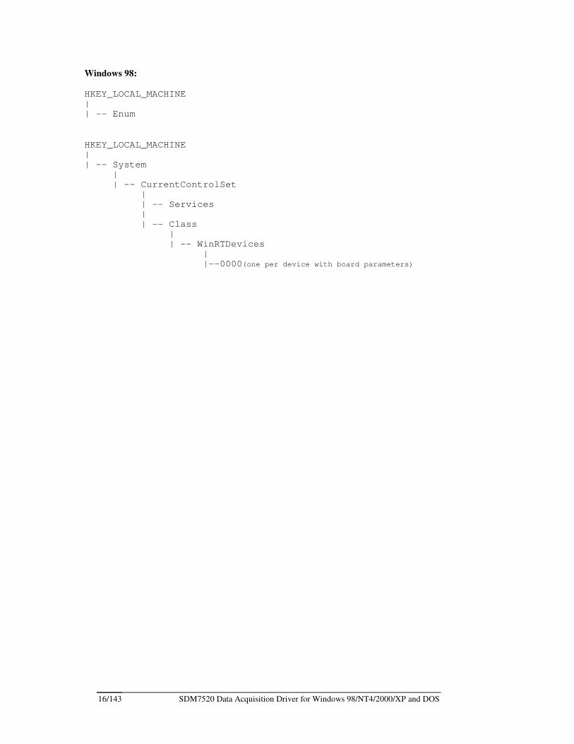
Windows 98:
HKEY_LOCAL_MACHINE | | -- Enum HKEY_LOCAL_MACHINE | | -- System | | -- CurrentControlSet | | -- Services | | -- Class | | -- WinRTDevices | |--0000(one per device with board parameters)
SDM7520 Data Acquisition Driver for Windows 98/NT4/2000/XP and DOS 17/143
SDM7540 Features
Measurement Scenarios Through selecting different options for A/D Conversion Trigger (SetConversionSelect7540), Burst Clock Start Trigger (SetBurstStart7540), Pacer Clock Start/Stop Trigger (SetPacerStart7540/SetPacerStop7540) and creating different Channel-Gain Tables, you have innumerable sampling scenarios. The following bullets try to enumerate only the most frequently used measurement setups. � Single Conversion
In this mode, a single channel is sampled whenever StartConversion7540 is called. The Channel Gain Latch (see WriteCGTLatch7540) specifies the channel to sample. This is the easiest scenario of all. It can be used in a variety of applications, such as sample every time a key is pressed on the keyboard, sample with each iteration of a loop, or watch the system clock and sample every five seconds.
� Multiple Conversions In this mode, conversions are continuously performed at the rate of the Pacer Clock, or other selected A/D Conversion Signal rate. The pacer clock can be internal or external. The maximum rate supported by the board is 1.25MHz. The Pacer Clock can be turned on and off using any of the start and stop triggering modes using the functions SetPacerStart7540 and SetPacerStop7540. If you use the internal pacer clock, you must program it to run at the desired rate (SetPacerClock7540). This mode is ideal for filling arrays, acquiring data for a specified period, and taking a specified number of samples.
� Random Channel Scan In this mode, the Channel-Gain Table is incrementally scanned through, with each selected A/D Conversion Signal pulse starting a conversion at the channel and gain specified in the current table entry. Before starting a conversion sequence Channel Gain Table, you need to load the table with the desired data. Then make sure that the Channel-Gain Table is enabled by the function EnableCGT7540. This enables the A/D portion of the Channel Gain Table. If you are using the Digital Table as well, you must also enable this using the function EnableCGTDigital7540. Each rising edge of selected A/D Conversion Signal starts a conversion using the current Channel Gain data and then increments to the next position in the table. When the last entry is reached, the next pulse starts the table over again.
� Programmable Burst In this mode, a single trigger initiates a scan of the entire Channel-Gain Table. Before starting a burst of the Channel-Gain Table, you need to load the table with the desired data. Then enable the Channel-Gain Table by EnableCGT7540. This enables the A/D portion of the channel-gain table. If you are using the Digital Table as well, you must also call EnableCGTDigital7540. Burst is used when you want one sample from a specified number of channels for each trigger. The burst trigger starts the Burst Clock and the Burst Clock initiates each conversion. At high speeds, the burst mode emulates simultaneous sampling of multiple input channels. For time critical simultaneous sampling applications, a simultaneous sample-and-hold board can be used (SS8 eight-channel boards are available from RTD Embedded Technologies).
SDM7520 Data Acquisition Driver for Windows 98/NT4/2000/XP and DOS 18/143
� Programmable Multi-Scan This mode - when the A/D Conversion Start Signal is the Burst Clock - lets you scan the Channel Gain Table after a Burst Clock Start Signal. When the Channel Gain Table is empty, the Burst Clock is stopped, and will wait for a new Start Signal.
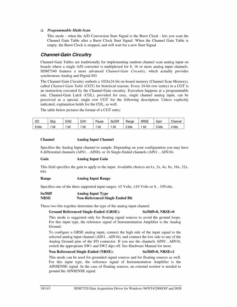
Channel-Gain Circuitry Channel-Gain Tables are traditionally for implementing random channel scan analog input on boards where a single A/D converter is multiplexed for 8, 16 or more analog input channels. SDM7540 features a more advanced Channel-Gain Circuitry, which actually provides synchronous Analog and Digital I/O. The Channel-Gain Circuitry embeds a 1024x24 bit on-board memory (Channel Scan Memory), called Channel-Gain Table (CGT) for historical reasons. Every 24-bit row (entry) in a CGT is an instruction executed by the Channel-Gain circuitry. Execution happens at a programmable rate. Channel-Gain Latch (CGL), provided for easy, single channel analog input, can be perceived as a special, single row CGT for the following description. Unless explicitly indicated, explanation holds for the CGL, as well. The table below pictures the format of a CGT entry:
DO Skip D/A2 D/A1 Pause Se/Diff Range NRSE Gain Channel
8 bits 1 bit 1 bit 1 bit 1 bit 1 bit 2 bits 1 bit 3 bits 4 bits
Channel Analog Input Channel
Specifies the Analog Input channel to sample. Depending on your configuration you may have 8 differential channels (AIN1…AIN8), or 16 Single-Ended channels (AIN1…AIN16)
Gain Analog Input Gain
This field specifies the gain to apply to the input. Available choices are1x, 2x, 4x, 8x, 16x, 32x, 64x
Range Analog Input Range
Specifies one of the three supported input ranges: ±5 Volts, ±10 Volts or 0…10Volts.
Se/Diff Analog Input Type NRSE Non-Referenced Single Ended Bit
These two bits together determine the type of the analog input channel. Ground Referenced Single-Ended (GRSE): Se/Diff=0, NRSE=0 This mode is suggested only for floating signal sources to avoid the ground loops. For this input type, the reference signal of Instrumentation Amplifier is the Analog Ground. To configure a GRSE analog input, connect the high side of the input signal to the selected analog input channel (AIN1...AIN16), and connect the low side to any of the Analog Ground pins of the I/O connector. If you use the channels AIN9…AIN16, switch the appropriate SW1 and SW2 dips off. See Hardware Manual for more. Non Referenced Single-Ended (NRSE): Se/Diff=0, NRSE=1 This mode can be used for grounded signal sources and for floating sources as well. For this input type, the reference signal of Instrumentation Amplifier is the AINSENSE signal. In the case of floating sources, an external resistor is needed to ground the AINSENSE signal.
SDM7520 Data Acquisition Driver for Windows 98/NT4/2000/XP and DOS 19/143
To configure an NRSE analog input, connect the high side of the input signal to the selected analog input channel (AIN1…AIN16), and connect the low side to the AINSENSE pin of the I/O connector Differential (DIFF): Se/Diff=1, NRSE=x This mode can be useful when the shielding of the signal is important. In differential mode, you use two analog input channels of the board for an analog input. AINx and AINx+8, also referred to as AINx+ and AINx-, can be used in couple for a differential analog input. This way you may have up to 8 differential analog inputs. For this input type, the reference signal of Instrumentation Amplifier is the AIN- signal. To configure an NRSE analog input, connect the high side of the analog input to the selected analog input channel (AIN1+…AIN8+), and connect the low side to the corresponding AIN- pin (AIN1-/AIN9…AIN8-/AIN16). See Hardware Manual for more.
Pause Pause Bit
If this bit is set and pausing is enabled by the EnableCGTPause7540 function, execution of the Channel-Gain Table stops after executing this entry. Execution is resumed with the next CGT entry when the programmed Pacer Clock start trigger occurs.
EXAMPLE: Pause Bit can be used when you have two sequence of entries, each to be executed on a different event (trigger). Suppose that CGT is driven by the Pacer Clock, and the Pacer Clock is started on the External Trigger. The External Trigger comes from a device, whose pulses indicate two different events. Odd pulses indicate an event, on which you want to react by sampling AIN1 and AIN2, on even pulses you want to sample AIN3, AIN4 and AIN5. In this case, you would create a 5 entry CGT:
Entry #1: AIN1, Pause Bit = 0 Entry #2: AIN2, Pause Bit = 1 Entry #3: AIN3, Pause Bit = 0 Entry #4: AIN4, Pause Bit = 0 Entry #5: AIN5, Pause Bit = 1
In this case, the first pulse on the External Trigger line starts executing the CGT at the rate of the Pacer Clock. After executing the first two entries, execution stops and is waiting for the next External Trigger pulse. The second pulse resumes execution, and entries #3, #4 and #5 are executed at the rate of the Pacer Clock. Execution pauses again, after executing entry #5. A third External trigger pulse continues execution with entry #1, and so on.
NOTE: When the Channel-Gain Latch is used, or in burst mode, Pause Bit is ignored.
D/A1 D/A2 D/A Update Bits
These bits can be used to simultaneously update the D/A converter(s) with the sampling of the appropriate analog input channel. When a D/A Update Bit is set, a D/A update signal is generated when A/D conversion starts.
SDM7520 Data Acquisition Driver for Windows 98/NT4/2000/XP and DOS 20/143
Skip Skip Bit
When the Skip Bit is set, the entry is skipped, which means that the A/D conversion is performed but the resulting sample is not written into the A/D FIFO. This feature provides a way to sample multiple channels at different rates without saving unwanted data.
EXAMPLE: In this example, we want to sample AIN1 in every second and AIN4 in every three seconds. For this end, we must create CGT with six entries:
Entry #1: AIN1, Skip Bit = 0 Entry #2: AIN4, Skip Bit = 1 Entry #3: AIN1, Skip Bit = 0 Entry #4: AIN4, Skip Bit = 1 Entry #5: AIN1, Skip Bit = 0 Entry #6: AIN4, Skip Bit = 0
Next, we set the Pacer Clock to run at 2 Hz (0.5 seconds). This allows us to sample each channel once per second, the maximum sampling rate required by one of the channels (pacer clock rate = number of different channels sampled x fastest sample rate).
The first Pacer Clock pulse starts an A/D conversion according to the parameters set in the first entry of the Channel-Gain Table, and each successive clock pulse incrementally steps through the table entries. The first clock pulse takes a sample on AIN1. The second pulse looks at the second entry in the table and sees that the Skip Bit is set. Sample is taken, but is not stored in the FIFO. The third pulse takes a sample on AIN1 again, the fourth pulse skips the next entry, and the fifth pulse takes our third reading on AIN1. On the sixth pulse, the Skip Bit is disabled, AIN4 is sampled and sample is stored to the FIFO. Then the sequence starts over again with entry #1. Samples are not stored when they are not wanted, saving memory and eliminating the need to throw away unwanted data.
NOTE: When the Channel-Gain Latch is used, Skip Bit is ignored.
When using the Channel Gain Table, you should group your entries to maximize the throughput of your module. Low-level input signals and varying gains are likely to drop the throughput rate because low level inputs must drive out high level input residual signals. To maximize throughput: � Keep channels configured for a certain range grouped together, even if they are out of
sequence. � Use external signal conditioning if you are performing high speed scanning of low level
signals. This increases throughput and reduces noise. � If you have room in the channel-gain table, you can make an entry twice to make sure that
sufficient settling time has been allowed and an accurate reading has been taken. Set the skip bit for the first entry so that it is ignored.
� For best results, do not use the channel-gain table when measuring steady-state signals. Use the single convert mode to step through the channels.
Interrupts The SDM7540 features a Priority Interrupt Controller with interrupt-overrun protection.
SDM7520 Data Acquisition Driver for Windows 98/NT4/2000/XP and DOS 21/143
Controller can receive interrupt request from up to 15 sources. These 15 sources cover the most important internal signals of the board plus 3 external signals (highest priority interrupt source comes first): � A/D FIFO Write
Interrupt is generated when sample enters the A/D FIFO. This interrupt can be used for reading and processing samples real-time.
� CGT Reset Interrupt is generated when the Channel-Gain Table recycles execution to the first table entry. This interrupt can be used for reading and processing a burst of samples from different channels real-time.
� CGT Pause Interrupt is generated when Channel-Gain Table execution is paused waiting for a new trigger.
� About Counter Countdown Interrupt is generated when the About Counter counts down to zero. This interrupt can be used to detect (and react on) the end of sampling when doing Pre/Port Triggering.
� Delay Counter Countdown Interrupt is generated when the Delay Counter counts down to zero. This interrupt can be used to detect (and react on) the actual start of sampling when doing Pre/Port Triggering.
� A/D Sample Counter Countdown � Interrupt is generated when the A/D Sample Counter counts down to zero. � D/A1 Update Counter Countdown � D/A2 Update Counter Countdown
Interrupt is generated when the D/A1 or D/A2 Update Counter counts down to zero. This interrupt can be used to count D/A conversions and do something on a timely basis, e.g., writing new data to the D/A FIFO.
� User Timer/Counter 1 Out � User Timer/Counter 1 Out, inverted � User Timer/Counter 2 Out
Interrupt is generated on the ticks of User T/C1 (i.e., when the counter counts down to zero). This interrupt gives you a general-purpose means of measuring real time, frequency, or counting events. It is also intended to use for Pulse output generation.
� Digital Interrupt Interrupt is generated when the Advanced Digital Trigger signals a Digital Interrupt. This interrupt can be used to detect (and react on) certain patterns on Digital Input Port 0.
� External Interrupt � Interrupt is generated on the rising edge of the External Interrupt pin of the I/O connector.
This interrupt is intended for exporting events from an external device. External Trigger rising-edge
� External Trigger falling-edge Interrupt is generated on a rising/falling edge of the External Trigger pin. This interrupt is intended for the Gated Mode operation of the Pacer Clock.
Because of the several interrupt sources on the board, a Priority Interrupt Controller was built to assure even usage all of the interrupt sources.

SDM7520 Data Acquisition Driver for Windows 98/NT4/2000/XP and DOS 22/143
When the Interrupt Controller receives an interrupt request, it transmits it to the PC Interrupt Controller (to the IRQ line, which is assigned to the board by the operating system). In the Interrupt Service Routine, reading the Interrupt Status Register via a call to GetITStatus7540, you can identify the causing interrupt source. In this register, there is a single non-zero bit that indicates the signaling interrupt source. If more than one interrupt source generates an interrupt at the same time, this register will indicate the highest priority one. The lower priority request is queued and will appear after acknowledging the higher priority one. After identifying the source, the interrupt can be serviced. After servicing, the request must be acknowledged by calling ClearITMask7540. Failing to do this makes the same interrupt reoccur repeatedly. In normal operation, the next interrupt request comes later than acknowledging the current one. However, if the next interrupt comes before acknowledging the current one, i.e., interrupt overrun occurs, you must be aware of it. For this situation, the SDM7540 has an Interrupt Overrun Register. Reading this register (see ReadITOverrun7540) after acknowledging the request enables you to determine a possible interrupt overflow. To service interrupts with the SDM7540 driver you do not have to deal with all these chores. Actually, in Windows when you install your interrupt handler, it is not a real Interrupt Service Routine, since you can not do that under Windows 98/2000/XP. Your handler is an ordinary routine, which is called by the real Interrupt Service Routine implemented by the SDM7540 driver. The driver’s Interrupt Service Routine schedules your interrupt handler for execution as a separate thread, acknowledges the interrupt to the board’s interrupt controller and returns. After returning, the scheduled thread starts executing your interrupt handler. In DOS your ISR is a real interrupt service routine.
Pre and Post Triggering SDM7540 offers various triggers for pre/post (about) triggering. The triggering mechanism, built around the Pacer/Burst Clock circuitry, lets you implement various triggering schemes. � Pre-Triggering
Pre-triggering scheme enables you to start sampling with some delay after an event (trigger).
This scheme can be useful when you do not want the first couple of samples after the important event. This can be the case when you know that these samples are noisy or meaningless because of settling issues. This scheme is realized by using the Delay Counter. Follow the steps below to set up for this scheme: 1. Set up the Pacer Clock to start delayed on the desired event.
SetPacerStart7540(hBoard,PCLK_START_D_xxx);
2. Initialize the Delay Counter for the required number of samples to wait (Delay Counter counts at the rate of the Pacer Clock).
SetupDelayCounter7540(hBoard,samples);
Start Trigger
sampling
SDM7520 Data Acquisition Driver for Windows 98/NT4/2000/XP and DOS 23/143
3. Arm the Pacer Clock to be ready for receiving the start trigger. StartPacer7540(hBoard);
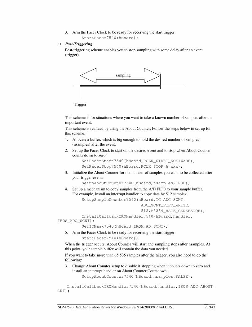
� Post-Triggering Post-triggering scheme enables you to stop sampling with some delay after an event (trigger).
This scheme is for situations where you want to take a known number of samples after an important event. This scheme is realized by using the About Counter. Follow the steps below to set up for this scheme: 1. Allocate a buffer, which is big enough to hold the desired number of samples
(nsamples) after the event. 2. Set up the Pacer Clock to start on the desired event and to stop when About Counter
counts down to zero. SetPacerStart7540(hBoard,PCLK_START_SOFTWARE);
SetPacerStop7540(hBoard,PCLK_STOP_A_xxx);
3. Initialize the About Counter for the number of samples you want to be collected after your trigger event.
SetupAboutCounter7540(hBoard,nsamples,TRUE);
4. Set up a mechanism to copy samples from the A/D FIFO to your sample buffer. For example, install an interrupt handler to copy data by 512 samples:
SetupSampleCounter7540(hBoard,TC_ADC_SCNT,
ADC_SCNT_FIFO_WRITE,
512,M8254_RATE_GENERATOR);
InstallCallbackIRQHandler7540(hBoard,handler, IRQS_ADC_SCNT);
SetITMask7540(hBoard,IRQM_AD_SCNT);
5. Arm the Pacer Clock to be ready for receiving the start trigger. StartPacer7540(hBoard);
When the trigger occurs, About Counter will start and sampling stops after nsamples. At this point, your sample buffer will contain the data you needed. If you want to take more than 65,535 samples after the trigger, you also need to do the following: 3. Change About Counter setup to disable it stopping when it counts down to zero and
install an interrupt handler on About Counter Countdown. SetupAboutCounter7540(hBoard,nsamples,FALSE);
InstallCallbackIRQHandler7540(hBoard,handler,IRQS_ADC_ABOUT_CNT);
Trigger
sampling
SDM7520 Data Acquisition Driver for Windows 98/NT4/2000/XP and DOS 24/143
6. In the About Counter interrupt handler, count the Countdowns and enable About Counter to stop when the required number of samples has been taken.
EnableAcntStop7540(hBoard,TRUE);
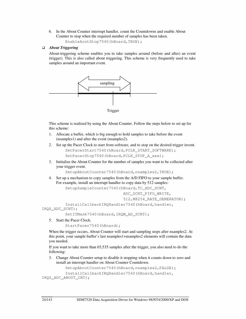
� About Triggering About-triggering scheme enables you to take samples around (before and after) an event (trigger). This is also called about triggering. This scheme is very frequently used to take samples around an important event.
This scheme is realized by using the About Counter. Follow the steps below to set up for this scheme: 1. Allocate a buffer, which is big enough to hold samples to take before the event
(nsamples1) and after the event (nsamples2). 2. Set up the Pacer Clock to start from software, and to stop on the desired trigger invent.
SetPacerStart7540(hBoard,PCLK_START_SOFTWARE);
SetPacerStop7540(hBoard,PCLK_STOP_A_xxx);
3. Initialize the About Counter for the number of samples you want to be collected after your trigger event.
SetupAboutCounter7540(hBoard,nsamples2,TRUE);
4. Set up a mechanism to copy samples from the A/D FIFO to your sample buffer. For example, install an interrupt handler to copy data by 512 samples:
SetupSampleCounter7540(hBoard,TC_ADC_SCNT,
ADC_SCNT_FIFO_WRITE,
512,M8254_RATE_GENERATOR);
InstallCallbackIRQHandler7540(hBoard,handler, IRQS_ADC_SCNT);
SetITMask7540(hBoard,IRQM_AD_SCNT);
5. Start the Pacer Clock. StartPacer7540(hBoard);
When the trigger occurs, About Counter will start and sampling stops after nsamples2. At this point, your sample buffer’s last nsamples1+nsamples2 elements will contain the data you needed. If you want to take more than 65,535 samples after the trigger, you also need to do the following: 3. Change About Counter setup to disable it stopping when it counts down to zero and
install an interrupt handler on About Counter Countdown. SetupAboutCounter7540(hBoard,nsamples2,FALSE);
InstallCallbackIRQHandler7540(hBoard,handler, IRQS_ADC_ABOUT_CNT);
Trigger
sampling
SDM7520 Data Acquisition Driver for Windows 98/NT4/2000/XP and DOS 25/143
6. In the About Counter interrupt handler, count the Countdowns and enable About Counter to stop when the required number of samples has been taken.
EnableAcntStop7540(hBoard,TRUE);
Advanced Digital Trigger The bit-programmable Digital I/O Port 0 supports two Advanced Digital Interrupt modes. The port can be programmed to generate an interrupt when selected port lines match a programmed value (match mode) or when any of the selected lines changes (event mode). Mode is selected by the SetDIO0CompareMode7540 function. When Advanced Digital Interrupt modes are enabled (see EnableDIO0Irq7540), the digital lines are sampled at either at 8 MHz or at the rate of User Timer/Counter 1. Clock is selected by the SetDIO0Clock7540 function. Only lines enabled in the Mask Register (set by SetDIO0Mask7540) take part in monitoring. With each clock pulse, the digital circuitry looks at the state of the next Port 0 bits. To provide noise rejection and prevent erroneous interrupt generation because of noise spikes on the digital lines, a change in the state of any bit must be seen for two edges of a clock pulse to be recognized by the circuit. In Event Mode, the enabled Port 0 input lines are monitored for a change. When any of these lines change, an interrupt is generated and the input pattern is latched into the Compare Register. You can read the contents of this register with GetDIO0CompareValue7540 to see which bit caused the interrupt to occur. In Match Mode, the enabled Port 0 input lines are monitored for the value programmed in the Compare Register with SetDIO0CompareValue7540 to occur. When lines match this value, an interrupt is generated. When Advanced Digital Interrupt mode is not enabled (see EnableDIO0Irq7540), the Mask Register can be used to preserve a bit’s state, regardless of the digital data written to Port 0. In addition, external data can be strobed into Port 0 by connecting a trigger pulse through the External Pacer Clock pin at the External I/O Connector. This data can be read from the Compare Register with GetDIO0CompareValue7540.
Synchron Bus Synchron Bus (SyncBus, for short) is a three-line bus for synchronized multi-board operation. A SyncBus line enables you to export/import signals to/from other boards. The other boards do not need to be SDM7540 or compatibles. Actually, you can use SyncBus for any purpose and from any place which can make use of a digital signal. A SyncBus line may have a single source and may have one or more users (including the source board). To configure a line you must select a signal (source) to put it on the line. To be more technical, consider the following exemplary situation.
EXAMPLE: You have 3 SDM7540 boards, A, B and C. You want board A’s Pacer Clock signal to be the D/A Update signal on board B, and the Burst Clock start signal on board C. This case you would do the following steps on the three boards:
Board A
1. Set SyncBus line 0 source to Pacer Clock: SetSbus0Source7540(hBoard,SBUS0_PCLK);
2. Enable SyncBus line 0: EnableSbus07540(hBoard,TRUE);
Board B
Set D/A1 Update Source to SyncBus line 0:
SDM7520 Data Acquisition Driver for Windows 98/NT4/2000/XP and DOS 26/143
SetDAC1Start7540(hBoard,DAC_START_SBUS0);
Board C
Set Burst Clock start trigger to SyncBus line 0: SetBurstStart7540(hBoard,BCLK_START_SBUS0);
To deconstruct this buildup (remove the Pacer Clock signal from line 0), you would do the following steps on the three boards:
Board A
Disable SyncBus line 0. EnableSbus07540(hBoard,FALSE);
Board B, C
Need to do nothing. D/A1 on board B, and Burst Clock on board C automatically seize to receive triggers on SyncBus line 0.Disable SyncBus line 0.
Data transfer with DMA The SDM7540 board provides two independent DMA channel with various modes to perform fast data transfer from the board to the PC memory or from the PC memory to the board. In Windows at the startup of the PC the SDM7540 driver allocates memory for DMA transfers. The default size of the DMA memory is 0x10000 bytes. To change this value do the following:
- change the DMACommonBufferSize value in the registry with the regedit.exe program and reboot the PC.
To setup the DMA transfer there are some driver calls to perform:
- InstallDMA7540: setup the driver’s DMA handling, get information about the DMA buffer address and length.
- SetupDMA7540: setup the direction, transfer byte count, DMA mode and source. - StartDMA07540/ StartDMA17540: start the DMA transfer. - DeInstallDMA7540: remove the DMA handler routine.
There are three basic DMA modes, which can be combined together:
- Normal mode: the data transfer initiated with software command (StartDMA07540/ StartDMA17540). After this command the hardware transfers the data from the source to the destination memory area.
- Demand mode: the data transfer starts on a programmable hardware event. The data transfer must precede a StartDMA07540/ StartDMA17540 command.
- Chaining mode: in this mode the DMA works under the control of chained descriptor blocks. Each descriptor block contains the DMA transfer direction, source and destination address, byte count and the address of the next descriptor block. The DMA continues to work until it reads an end of chain bit in the last descriptor block. This mode is useful to perform DMA transfers with different directions or transfer data from various addresses. Note that chaining mode is not supported in DOS.
In the example programs can be found examples on normal, demand and chaining mode DMA transfers with different directions.

SDM7520 Data Acquisition Driver for Windows 98/NT4/2000/XP and DOS 27/143

SDM7520 Data Acquisition Driver for Windows 98/NT4/2000/XP and DOS 29/143
Driver API Function Groups
Driver Initialization Functions OpenBoard7540 CloseBoard7540 GetErrorStatus7540
General Board Control Functions InitBoard7540 ClearAllIO7540 IsBusMaster7540 ReadFirmwareVersion7540
FIFO Manipulation GetFifoStatus7540 IsADFIFOEmpty7540 IsADFifoHalfFull7540 IsADFifoFull7540 IsDINFifoEmpty7540 IsDINFifoHalfFull7540 IsDINFifoFull7540 IsDAC1FifoEmpty7540 IsDAC1FifoHalfFull7540 IsDAC1FifoFull7540 IsDAC2FifoEmpty7540 IsDAC2FifoHalfFull7540 IsDAC2FifoFull7540 ClearDinFifo7540 ClearADFIFO7540 ResetDAC1Fifo7540 ClearDAC1FIFO7540 ResetDAC2Fifo7540 ClearDAC2FIFO7540 ReadADData7540 ReadADDataWithMarker7540 ReadDinFifo7540 WriteDac1Fifo7540 WriteDac2Fifo7540 LoadDAC17540 LoadDAC27540
A/D Converter StartConversion7540 SetConversionSelect7540
Channel-Gain Table Manipulation WriteCGTAnalog7540 WriteCGTLatch7540 WriteCGTDigital7540 EnableCGT7540 EnableCGTDigital7540
SDM7520 Data Acquisition Driver for Windows 98/NT4/2000/XP and DOS 30/143
EnableCGTPause7540 ResetCGT7540 ClearCGT7540 SetupCgtRow7540 SetChannelGain7540
Pacer Clock Handling StartPacer7540 StopPacer7540 ReadPacer7540 SetPacerStart7540 SetPacerStop7540 SetPacerRepeat7540 SetPclkSize7540 SetPacerSource7540 SetPacerRate7540 SetPacerRateF7540 SetPacerClock7540 SetPacerClockF7540 SelectPacerClockPrimaryClock7540
Burst Clock Handling StartBurst7540 SetBurstStart7540 SetBurstRate7540 SetBurstRateF7540 SetupBurst7540 SetupBurstF7540 SelectBurstClockPrimaryClock7540
Delay Counter Functions LoadDcnt7540 SetupDelayCounter7540
About Counter Functions EnableAcntStop7540 LoadAcnt7540 GetAcntCount7540 SetupAboutCounter7540
Sample Counter Functions SetAdcntSource7540 GetAdcntCount7540 SetupSampleCounter7540 ReadSampleCounter7540 LoadAdcnt7540
D/A Converter UpdateDAC17540 UpdateDAC27540 UpdateAllDAC7540 SetDACDivisor7540
SDM7520 Data Acquisition Driver for Windows 98/NT4/2000/XP and DOS 31/143
SetDACRate7540 SetDACRateF7540 GetDACDivisor7540 DACClockStartSelect7540 DACClockStopSelect7540 DACClockFreeRun7540 SelectDACClockPrimaryClock7540 StartDACClock7540 StopDACClock7540 SetDAC1Range7540 SetDAC1Start7540 SetDAC1Cycle7540 SetDAC2Range7540 SetDAC2Start7540 SetDAC2Cycle7540 LoadUcnt17540 LoadUcnt27540 SetupDAC7540
Digital I/O Functions ClearDIO7540 ClearDIO0IrqStatus4 EnableDIO0Irq7540 GetDIO0Clock7540 GetDIO0CompareMode7540 GetDIO0CompareValue7540 GetDIO0Direction7540 GetDIO1Direction7540 GetDIO0Mask7540 GetDIOStatus7540 PollDIO07540 ReadDIO07540 ReadDIO17540 SelectDIO0Register7540 SetDIO0Clock7540 SetDIO0CompareMode7540 SetDIO0CompareValue7540 SetupPort07540 SetupPort17540 SetDIO0Direction7540 SetDIO1Direction7540 SetDIO0Mask7540 WriteDIO07540 WriteDIO17540
High-Speed Digital Input Functions StartHdin7540 SetHdinStart7540
User Input/Output Functions ReadUserInput7540 WriteUserOutput7540 SetUout0Source7540
SDM7520 Data Acquisition Driver for Windows 98/NT4/2000/XP and DOS 32/143
SetUout1Source7540
User Timer-Counter Functions GetTimerStatus7540 SetUtc0Clock7540 SetUtc0Gate7540 SetUtc1Clock7540 SetUtc1Gate7540 SetUtc2Clock7540 SetUtc2Gate7540 Set8254Divisor7540 Set8254Mode7540 Get8254Mode7540 Get8254Count7540 Get8254Status7540 SetupTimerCounter7540 ReadTimerCounter7540
Interrupt Handling GetITStatus7540 SetITMask7540 ClearITMask7540 ReadITOverrun7540 ClearITOverrun7540 SetEintPolarity7540 InstallCallbackIRQHandler7540 RemoveIRQHandler7540
Synchron Bus Configuration Functions SetSbus0Source7540 EnableSbus07540 SetSbus1Source7540 EnableSbus17540 SetSbus2Source7540 EnableSbus27540 SetupSbus7540
External Trigger Configuration Functions SetEtrgPolarity7540
DMA functions InstallDMA7540 DeInstallDMA7540 SetupDMA7540 SetupDirectDMA7540 ShareDMABuffer7540 SetupChainedDMA7540 SetFirstDescriptorBlock7540 SetFirstDirectDescriptorBlock7540 SetNextDescriptorBlock7540 SetNextDirectDescriptorBlock7540
SDM7520 Data Acquisition Driver for Windows 98/NT4/2000/XP and DOS 33/143
SetLastDescriptorBlock7540 SetLastDirectDescriptorBlock7540 StartDMA07540 StartDMA17540 StartChainedDMA07540 StartChainedDMA17540 AbortDMA07540 AbortDMA17540 GetDMA0Status7540 GetDMA1Status7540 GetDMADoneChannel7540 IsDMA0Done7540 IsDMA1Done7540 ResetDMA0State7540 ResetDMA1State7540
McBSP Port Control Functions McBSPADControl7540 McBSPDAControl7540
Calibration and DSP Control Functions StartCalibration7540
isCommandDone7540 MakeSRAMAvailable7540 MakeLAS1Available7540 ReadSRAM7540 StartAutocalUpgrade7540 WriteSRAM7540 GetAttention7540 EraseInternalFlash7540 GetDSPResultCode7540 LoadFailsafe7540 GetAutocalVersion7540 GetBootLdrVersion7540 GetBoardTemp7540
SDM7520 Data Acquisition Driver for Windows 98/NT4/2000/XP and DOS 34/143
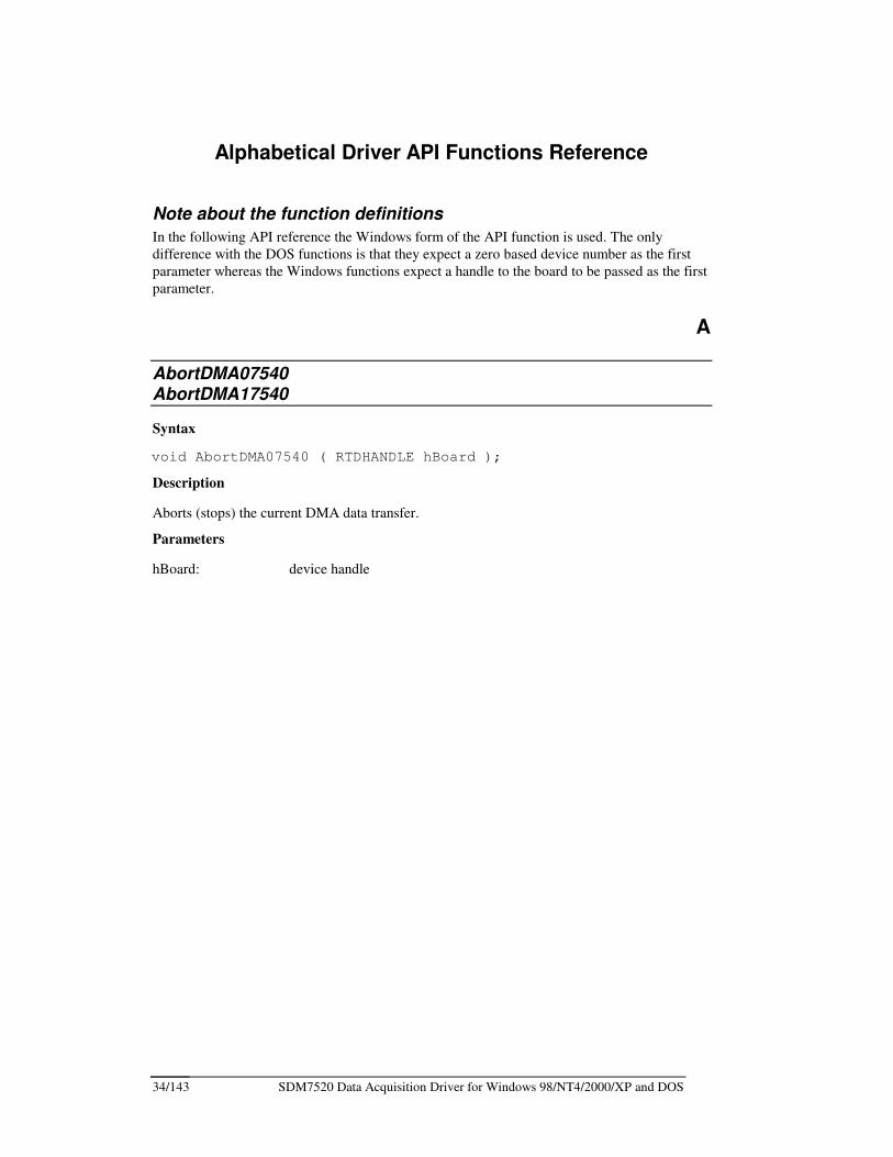
Alphabetical Driver API Functions Reference
Note about the function definitions In the following API reference the Windows form of the API function is used. The only difference with the DOS functions is that they expect a zero based device number as the first parameter whereas the Windows functions expect a handle to the board to be passed as the first parameter.
A
AbortDMA07540 AbortDMA17540
Syntax
void AbortDMA07540 ( RTDHANDLE hBoard );
Description
Aborts (stops) the current DMA data transfer.
Parameters
hBoard: device handle
SDM7520 Data Acquisition Driver for Windows 98/NT4/2000/XP and DOS 35/143
C
ClearADFIFO7540
Syntax
void ClearADFIFO7540 (RTDHANDLE hBoard);
Description
Dispose all samples from the A/D FIFO.
NOTE: Reading from an empty FIFO (e.g., with ReadADData7540, ReadADDataWithMarker7540) results in non-deterministic data.
Parameters
hBoard: device handle
ClearAllIO7540
Syntax
void ClearAllIO7540 (RTDHANDLE hBoard);
Description
Software reset of the board.
Parameters
hBoard: device handle
ClearCGT7540
Syntax
void ClearCGT7540 (RTDHANDLE hBoard);
Description
Clear A/D Channel-Gain Table. This function removes all entries from the CGT. Use this function before reprogramming the CGT. This is the only way to remove entries from the CGT. There is no way to insert /remove a single CGT entry or change it in place.
NOTE: This function clears the Digital part of the CGT.
Parameters
hBoard: device handle
SDM7520 Data Acquisition Driver for Windows 98/NT4/2000/XP and DOS 36/143
See Also
Channel-Gain Circuitry
ClearDAC1FIFO7540 ClearDAC2FIFO7540
Syntax
void ClearDAC1FIFO7540 (RTDHANDLE hBoard); void ClearDAC2FIFO7540 (RTDHANDLE hBoard);
Description
Remove all data from D/A1 or D/A FIFO. This function sets the update and the write pointer of the FIFO to the beginning of the FIFO. This means that the FIFO is ready to be filled with new data.
NOTE: Updating a D/A Converter (e.g., with UpdateDAC17540 ,UpdateDAC27540, UpdateAllDAC7540) when its FIFO is empty has no effect.
Parameters
hBoard: device handle
ClearDinFifo7540
Syntax
void ClearDinFifo7540 (RTDHANDLE hBoard);
Description
Remove all samples from the High Speed Digital Input FIFO.
NOTE: Reading from an empty FIFO (e.g., with ReadDinFifo7540) results in undeterministic data.
Parameters
hBoard: device handle
ClearDIO7540
Syntax
void ClearDIO7540 (RTDHANDLE hBoard);
Description
Reset the Digital I/O chip. It programs all I/O lines for input and programs the Advanced Digital Trigger for Event Mode.
NOTE: It does not clear a pending interrupt. You must make a call to ClearDIO0IrqStatus7540 explicitly.
SDM7520 Data Acquisition Driver for Windows 98/NT4/2000/XP and DOS 37/143
Parameters
hBoard: device handle
ClearDIO0IrqStatus7540
Syntax
void ClearDIO0IrqStatus7540 (RTDHANDLE hBoard);
Description
Clears the Digital IRQ status flag. You must acknowledge Digital Interrupts by calling this function. Failing to do this means that no more Digital Interrupts will be generated by the Digital I/O chip.
Parameters
hBoard: device handle
See Also
Advanced Digital Trigger
ClearITMask7540
Syntax
void ClearITMask7540 (RTDHANDLE hBoard, uint16 mask);
Description
Acknowledge interrupts from the specified interrupt sources.
NOTE: In Windows there is no need to call this function, because it is automatically called when you install an interrupt handler. However, if you do not install a handler for an interrupt source, but interrupts are enabled from that source (see SetITMask7540), you may need this function to acknowledge interrupts.
Parameters
hBoard: device handle mask: mask of interrupt sources for which to acknowledge interrupts: D0 (0x0001) ADC FIFO Write D1 (0x0002) Reset CGT
D2 (0x0004) reserved D3 (0x0008) Pause CGT D4 (0x0010) About counter out D5 (0x0020) Delay counter out D6 (0x0040) ADC Sample Counter D7 (0x0080) DAC1 Update Counter D8 (0x0100) DAC2 Update Counter D9 (0x0200) User TC1 out D10 (0x0400) User TC1 out, inverted D11 (0x0800) User TC2 out
SDM7520 Data Acquisition Driver for Windows 98/NT4/2000/XP and DOS 38/143
D12 (0x1000) Digital Interrupt D13 (0x2000) External Interrupt D14 (0x4000) External Trigger rising-edge D15 (0x8000) External Trigger falling-edge
ClearITOverrun7540
Syntax
void ClearITOverrun7540 (RTDHANDLE hBoard);
Description
Clear Interrupt Overrun Register. The Interrupt Overrun Register is for detecting interrupt overrun conditions. If an interrupt occurs from a source and another interrupt occurs from that source before the first interrupt is acknowledged, the appropriate bit in the Interrupt Overrun Register goes to 1 indicating overrun.
NOTE: In Windows, this function is automatically called on every interrupt if you install an interrupt handler.
Parameters
hBoard: device handle
CloseBoard7540
Syntax
BOOL CloseBoard7540 (RTDHANDLE hBoard, LPSTR szBuf);
Description
This routine is used to close a board. Call this function when you have finished using the board. CloseBoard7540 releases no longer needed system resources and the SDM7540 itself and makes them available for other applications.
NOTE: After closing a board, no driver functions may be called but OpenBoard7540.
Parameters
hBoard: device handle. szBuf: Message buffer to return error message if any error occurs during
closing the board.
Return Value
TRUE Board is closed successfully. FALSE There was an error while closing the board. See GetErrorStatus7540 for the error occurred.
SDM7520 Data Acquisition Driver for Windows 98/NT4/2000/XP and DOS 39/143
D
DACClockFreeRun7540
Syntax
void DACClockFreeRun7540(RTDHANDLE hBoard, BOOL runmode);
Description
DAC Clock Run Mode selection. On power-up the board starts with free running DAC clock. For the start/stop mode which is used with the one-cycle generation program, the run mode should be set to start/stop mode.
Parameters
hBoard: device handle runmode: DAC_CLK_FREERUN DAC_CLK_STARTSTOP
DACClockStartSelect7540
Syntax
void DACClockStartSelect7540(RTDHANDLE hBoard, uint16 data);
Description
DAC Clock Start Select. Selects the source signal that will start the DAC Clock. You must first have set the DAC Clock to start/stop mode by using DACClockFreeRun7540.
Parameters
hBoard: device handle data :
DAC_STARTCLOCK_SOFTPACER 0x0 Software Pacer Start (RD_LAS0+028h) DAC_STARTCLOCK_EXTTRIG 0x1 External Trigger DAC_STARTCLOCK_DIGINT 0x2 Digital Interrupt DAC_STARTCLOCK_UTC2 0x3 User TC2 out DAC_STARTCLOCK_SBUS0 0x4 // SyncBus 0 DAC_STARTCLOCK_SBUS1 0x5 // SyncBus 1 DAC_STARTCLOCK_SBUS2 0x6 // SyncBus 2
DAC_STARTCLOCK_SOFTWARE 0x7 // Software D/A Clock Start (RD_LAS0+0ch)
DACClockStopSelect7540
Syntax
void DACClockStopSelect7540(RTDHANDLE hBoard, uint16 data);
Description
DAC Clock Stop Select.. Selects the signal that will be used to stop the DAC Clock. You must first have set the DAC Clock to start/stop mode by using DACClockFreeRun7540.
Parameters
hBoard: device handle data :
SDM7520 Data Acquisition Driver for Windows 98/NT4/2000/XP and DOS 40/143
DAC_STOP_SOFTPACER 0x0 // Software Pacer Start (RD_LAS0+028h) DAC_STOP_EXTTRIG 0x1 // External Trigger DAC_STOP_DIGINT 0x2 // Digital Interrupt DAC_STOP_UTC2 0x3 // User TC2 out DAC_STOP_SBUS0 0x4 // SyncBus 0 DAC_STOP_SBUS1 0x5 // SyncBus 1 DAC_STOP_SBUS2 0x6 // SyncBus 2 DAC_STOP_SOFTWARE 0x7 // Software D/A Clock Start (RD_LAS0+0ch) DAC_STOP_DA1UPDATE 0x8 // D/A1 Update Counter
DAC_STOP_DA2UPDATE 0x9 // D/A2 Update Counter
DeInstallDMA7540
Syntax
BOOL DeInstallDMA7540(RTDHANDLE hBoard, int dma_channel );
Description
This routine is used to remove the DMA handler.
Parameters
hBoard: device handle dma_channel: DMA channel number (0/1)
Return Value
TRUE Board is closed successfully. FALSE There was an error while closing the board. See GetErrorStatus7540 for the error occurred.
SDM7520 Data Acquisition Driver for Windows 98/NT4/2000/XP and DOS 41/143
E
EnableAcntStop7540
Syntax
void EnableAcntStop7540 (RTDHANDLE hBoard, uint16 enable);
Description
Enable/disable About Counter to stop when it counts down to zero. Default setting is enabled. The About Counter is a 16-bit down counter that stops or reloads the initial count value after counting down to zero. The About Counter, counting at the rate of the Pacer Clock, can be used to count samples. When About Counter stop enabled, the counter stops when it counts down to zero. If you disable About Counter Stop, the counter keeps reloading the initial counter value when it reaches zero. In both cases, you may program the board to generate an interrupt.
Parameters
hBoard: device handle enable: 0 = Stop enabled 1 = Stop disabled
EnableCGT7540
Syntax
void EnableCGT7540 (RTDHANDLE hBoard, uint16 enable);
Description
Select Channel Gain Table or Channel-Gain Latch to use for A/D sampling.
Parameters
hBoard: device handle enable: CSC_LATCH (0)
Channel Gain Table disabled Channel Gain Latch enabled. CSC_CGT (1)
Channel Gain Table enabled Channel Gain Latch disabled.
See Also
Channel-Gain Circuitry, EnableCGTDigital7540.
EnableCGTDigital7540
Syntax
void EnableCGTDigital7540 (RTDHANDLE hBoard, uint16 enable);
SDM7520 Data Acquisition Driver for Windows 98/NT4/2000/XP and DOS 42/143
Description
Enable/disable Digital Table.
NOTE: This function has no effect if you use the Channel-Gain Latch.
Parameters
hBoard: device handle enable: FALSE (0)
Digital Table disabled, Digital I/O P1 port enabled. TRUE (1)
Digital Table enabled, Digital I/O P1 port disabled.
See Also
Channel-Gain Circuitry, EnableCGT7540
EnableCGTPause7540
Syntax
void EnableCGTPause7540 (RTDHANDLE hBoard, uint16 enable);
Description
Enable/disable using the Channel-Gain Table Pause Bit.
NOTE: Set the Pause Bit if you want to stop an entry in the table and wait for the next trigger. In burst mode, the pause bit is ignored.
Parameters
hBoard: device handle enable: FALSE (0) Disable interpreting CGT Pause Bit. TRUE (1) Enable interpreting CGT Pause Bit.
See Also
Channel-Gain Circuitry
EnableDIO0Irq7540
Syntax
void EnableDIO0Irq7540 (RTDHANDLE hBoard, BOOL enable);
Description
Enable/disable Bit Programmable Digital I/O to generate interrupts.
Parameters
hBoard: device handle enable: FALSE (0) disable TRUE (1) enable
SDM7520 Data Acquisition Driver for Windows 98/NT4/2000/XP and DOS 43/143
See Also
Advanced Digital Trigger
EnableSbus07540 EnableSbus17540 EnableSbus27540
Syntax
void EnableSbus07540 (RTDHANDLE hBoard, uint16 enable);
void EnableSbus17540 (RTDHANDLE hBoard, uint16 enable);
void EnableSbus27540 (RTDHANDLE hBoard, uint16 enable);
Description
Enable Synchron Bus line 0/1/2. This function enables the programmed Synchron Bus source to appear on the line. Calling it with enable=FALSE has the effect of removing the signal from the line. (In effect a disabled syncbus is an input and an enabled syncbus is an output)
NOTE: A Synchron Bus line may be enabled on one board only.
Parameters
hBoard: device handle enable: 0x1 = enable 0x0 = disable
See Also
Synchron Bus.
EraseInternalFlash7540
Syntax
void EraseInternalFlash7540(RTDHANDLE hBoard);
Description
Instruct the DSP boot loader program to erase internal flash memory. NOTE: Only the sectors containing the autocalibration program are erased. The boot loader is never erased.
Parameters
hBoard: device handle Returns None
SDM7520 Data Acquisition Driver for Windows 98/NT4/2000/XP and DOS 44/143
G
Get8254Count7540
Syntax
uint16 Get8254Count7540 (RTDHANDLE hBoard, int counter);
Description
Read current counter value of the 8254 Timer/Counter.
Parameters
hBoard: device handle counter: One of the 16-bit timer/counters of the board.
TC_PCLK 0 // Pacer Clock 0 TC_BCLK 2 // Burst Clock TC_ADC_SCNT 3 // A/D Sample counter TC_DAC1_UCNT 4 // D/A1 Update counter TC_DAC2_UCNT 5 // D/A2 Update counter TC_DCNT 6 // Delay Counter TC_ACNT 7 // About Counter TC_DAC_CLK 8 // DAC clock TC_UTC0 9 // 8254 TC Counter 0 User TC 0 TC_UTC1 10 // 8254 TC Counter 1 User TC 1
TC_UTC2 11 // 8254 TC Counter 2 User TC 2
Return Value
Current counter value of the 8254 Timer/Counter.
Get8254Mode7540
Syntax
uint8 Get8254Mode7540 (RTDHANDLE hBoard, int counter);
Description
Read back programmed operation mode of a 8254 Timer/Counter.
Parameters
hBoard: device handle counter: One of the 16-bit timer/counters of the board.
TC_PCLK 0 // Pacer Clock 0 TC_BCLK 2 // Burst Clock TC_ADC_SCNT 3 // A/D Sample counter TC_DAC1_UCNT 4 // D/A1 Update counter TC_DAC2_UCNT 5 // D/A2 Update counter TC_DCNT 6 // Delay Counter TC_ACNT 7 // About Counter TC_DAC_CLK 8 // DAC clock TC_UTC0 9 // 8254 TC Counter 0 User TC 0 TC_UTC1 10 // 8254 TC Counter 1 User TC 1
TC_UTC2 11 // 8254 TC Counter 2 User TC 2
Return Value Current operation mode of the 8254 Timer/Counter.
SDM7520 Data Acquisition Driver for Windows 98/NT4/2000/XP and DOS 45/143
M8254_EVENT_COUNTER 0 // Event Counter M8254_HW_ONE_SHOT 1 // Hardware-Retriggerable One-Shot M8254_RATE_GENERATOR 2 // Rate Generator
M8254_SQUARE_WAVE 3 // Square Wave Mode M8254_SW_STROBE 4 // Software Triggered Strobe
M8254_HW_STROBE 5 // Hardware Triggered Strobe (Retriggerable)
Get8254Status7540
Syntax
uint8 Get8254Status7540 (RTDHANDLE hBoard, int counter);
Description
Read status of a 8254 Timer/Counter.
Parameters
hBoard: device handle counter: One of the 16-bit timer/counters of the board.
TC_PCLK 0 // Pacer Clock 0 TC_BCLK 2 // Burst Clock TC_ADC_SCNT 3 // A/D Sample counter TC_DAC1_UCNT 4 // D/A1 Update counter TC_DAC2_UCNT 5 // D/A2 Update counter TC_DCNT 6 // Delay Counter TC_ACNT 7 // About Counter TC_DAC_CLK 8 // DAC clock TC_UTC0 9 // 8254 TC Counter 0 User TC 0 TC_UTC1 10 // 8254 TC Counter 1 User TC 1
TC_UTC2 11 // 8254 TC Counter 2 User TC 2
Return Value Current status of the 8254 Timer/Counter.
GetAttention7540
Syntax
bool GetAttention7540(RTDHANDLE hBoard);
Description
Checks that the Boot Loader is running on the DSP.
Parameters
hBoard: device handle
SDM7520 Data Acquisition Driver for Windows 98/NT4/2000/XP and DOS 46/143
Return Value
TRUE – Boot Loader code is running and DSP is ready for commands
FALSE – Boot Loader code us not running
GetAcntCount7540
Syntax
uint16 GetAcntCount7540 ( RTDHANDLE hBoard );
Description
Read the About Counter value.
Parameters
hBoard: device handle
Return Value
The current about counter value.
GetAdcntCount7540
Syntax
uint16 GetAdcntCount7540 ( RTDHANDLE hBoard );
Description
Read the A/D Sample Counter value.
Parameters
hBoard: device handle
Return Value
The current A/D sample counter value.
GetAutocalVersion7540
Syntax
void GetAutocalVersion7540(RTDHANDLE hBoard);
Description
Instruct the DSP boot loader program to return the version number of the autocalibration program. The boot loader requests the autocalibration program perform the action. NOTE: The version number is returned in SRAM with the major version number stored in SRAM + 0 and the minor version number stored in SRAM + 4.
SDM7520 Data Acquisition Driver for Windows 98/NT4/2000/XP and DOS 47/143
Parameters
hBoard: device handle
Return Value
None
GetBoardTemp7540
Syntax
int GetBoardTemp7540(RTDHANDLE hBoard);
Description
Return the temperature as indicated by the onboard temperature monitor.
Parameters
hBoard: device handle
Return Value
The current board temperature in celcius.
GetBootLdrVersion7540
Syntax
void GetBootLdrVersion7540(RTDHANDLE hBoard);
Description
Instruct the DSP boot loader program to return the version number of the boot loader program. NOTE: The version number is returned in SRAM with the major version number stored in SRAM + 0 and the minor version number stored in SRAM + 4.
Parameters
hBoard: device handle
Return Value
None
GetDACDivisor7540
Syntax
Uint32 GetDACDivisor7540 (RTDHANDLE hBoard);
SDM7520 Data Acquisition Driver for Windows 98/NT4/2000/XP and DOS 48/143
Description
Read the 24 bit wide DAC clock value.
Parameters
hBoard: device handle
Return Value
The actual DAC clock value.
GetDIO0Clock7540
Syntax
uint8 GetDIO0Clock7540 (RTDHANDLE hBoard);
Description
Read Clock set for the bit programmable Digital I/O (port 0).
Parameters
hBoard: device handle
Return Value
0 - 8 MHz On-board Oscillator 1 - User TC Counter 1
GetDIO0CompareMode7540
Syntax
uint8 GetDIO0CompareMode7540 (RTDHANDLE hBoard);
Description
Read port 0 compare mode.
Parameters
hBoard: device handle
Return Value
0 - Event Mode 1 - Match Mode
GetDIO0CompareValue7540
Syntax
uint8 GetDIO0CompareValue7540 (RTDHANDLE hBoard);
Description
Read pattern of Port 0 I/O lines for Digital Interrupt generation.
SDM7520 Data Acquisition Driver for Windows 98/NT4/2000/XP and DOS 49/143
Parameters
hBoard: device handle
Return Value
pattern
GetDIO0Direction7540
Syntax
uint8 GetDIO0Direction7540 (RTDHANDLE hBoard);
Description
Return programmed Digital I/O Port 0 line directions.
Parameters
hBoard: device handle
Return Value
8-bit direction mask: Bit = 0 – line is programmed for input Bit = 1 – line is programmed for output
GetDIO0Mask7540
Syntax
uint8 GetDIO0Mask7540 (RTDHANDLE hBoard);
Description
Return Digital Interrupt mask for Port 0 I/O lines.
Parameters
hBoard: device handle
Return Value
8-bit interrupt mask: Bit = 1 - line is disabled to take part in Digital Interrupt generation Bit = 0 - line is enabled to take part in Digital Interrupt generation
See Also
Advanced Digital Trigger
GetDIO1Direction7540
Syntax
uint8 GetDIO1Direction7540 (RTDHANDLE hBoard);
Description
Return Digital I/O Port 1 direction.
SDM7520 Data Acquisition Driver for Windows 98/NT4/2000/XP and DOS 50/143
Parameters
hBoard: device handle
Return Value
Bit 0 port direction 0 input 1 output
Bit 1..7 0
GetDIOStatus7540
Syntax
uint8 GetDIOStatus7540 (RTDHANDLE hBoard);
Description
Read Digital I/O status.
Parameters
hBoard: device handle
Return Value
D0..D1 register opened for programming D2 Port 1 direction (0 - input, 1 - output) D3 Digital IRQ Mode (0 - Event, 1 - Match) D4 Digital IRQ Enable (0 - disabled, 1 - enabled) D5 Digital Sample Clock Select (0 - 8MHz oscillator, 1 - User TC Counter 1) D6 Digital IRQ Status (0 - no IRQ, 1 - IRQ) D7 Strobe Status
See Also
Advanced Digital Trigger
GetDMA0Status7540 GetDMA1Status7540
Syntax
uint8 GetDMA0Status7540 ( RTDHANDLE hBoard );
uint8 GetDMA1Status7540 ( RTDHANDLE hBoard );
Description
Read DMA status register.
Parameters
hBoard: device handle
Return Value
Value of status register (DMA channel 0/1 command/status register).
SDM7520 Data Acquisition Driver for Windows 98/NT4/2000/XP and DOS 51/143
GetDMADoneChannel7540
Syntax unsigned char GetDMADoneChannel7540(RTDHANDLE hBoard);
Description This routine is used to determine which DMA channel generated the DMA done interrupt.
Parameters
hBoard: device handle
Return Value
1 if DMA channel 0 done 2 if DMA channel 1 done 3 if DMA channel 0 and DMA channel 1 done
GetDSPResultCode7540
Syntax
uint16 GetDSPResultCode7540(RTDHANDLE hBoard);
Description
Get the result code for the last command executed by the DSP.
Parameters
hBoard: device handle
Return Value
Result of last DSP command. Zero indicates success.
GetErrorStatus7540
Syntax
BOOL GetErrorStatus7540 (RTDHANDLE hBoard, LONG *ErrorCode);
Description
Return last error code for a given board and clears the internal error status variable (i.e., a second call to this function will return FALSE, indicating no error).
Parameters
hBoard: device handle ErrorCode: pointer to a location to return the error code.
Return Value
TRUE If there is an error. FALSE If there is no error.
SDM7520 Data Acquisition Driver for Windows 98/NT4/2000/XP and DOS 52/143
GetFifoStatus7540
Syntax
uint16 GetFifoStatus7540 (RTDHANDLE hBoard);
Description
Return the status of all board FIFO buffers.
Parameters
hBoard: device handle
Return Value
Bit 0 (0x0001) DAC1 FIFO not empty Bit 1 (0x0002) DAC1 FIFO not half empty Bit 2 (0x0004) DAC1 FIFO not full Bit 3 (0x0008) 0 (reserved) Bit 4 (0x0010) DAC2 FIFO not empty Bit 5 (0x0020) DAC2 FIFO not half empty Bit 6 (0x0040) DAC2 FIFO not full Bit 7 (0x0080) 0 (reserved) Bit 8 (0x0100) ADC FIFO not empty Bit 9 (0x0200) ADC FIFO not half empty Bit 10 (0x0400) ADC FIFO not full Bit 11 (0x0800) 0 (reserved) Bit 12 (0x1000) DIN FIFO not empty Bit 13 (0x2000) DIN FIFO not half empty Bit 14 (0x4000) DIN FIFO not full Bit 15 (0x8000) 0 (reserved) See FS_XXXX symbolic constants.
GetITStatus7540
Syntax
uint16 GetITStatus7540 (RTDHANDLE hBoard);
Description
Read Interrupt Status Register.
Parameters
hBoard: device handle
Return Value
Return a mask of interrupt sources which have a pending interrupt request (bit = 0-inactive, bit = 1-active): Bit 0 (0x0001) ADC FIFO Write Bit 1 (0x0002) Reset CGT Bit 2 (0x0004) reserved Bit 3 (0x0008) Pause CGT Bit 4 (0x0010) ADC FIFO half-full Bit 5 (0x0020) ADC FIFO full Bit 6 (0x0040) ADC Sample Counter Bit 7 (0x0080) DAC1 Update Counter
SDM7520 Data Acquisition Driver for Windows 98/NT4/2000/XP and DOS 53/143
Bit 8 (0x0100) DAC2 Update Counter Bit 9 (0x0200) User TC1 out Bit 10 (0x0400) User TC1 out, inverted Bit 11 (0x0800) User TC2 out Bit 12 (0x1000) Digital Interrupt Bit 13 (0x2000) External Interrupt Bit 14 (0x4000) External Trigger rising-edge Bit 15 (0x8000) External Trigger falling-edge
GetTimerStatus7540
Syntax
uint16 GetTimerStatus7540 (RTDHANDLE hBoard);
Description
Read Timer Counters Status.
Parameters
hBoard: device handle
Return Value TS_PCLK_GATE 0x0001 // D0 - Pacer Clock Gate [0 - gated, 1 - enabled] TS_BCLK_GATE 0x0002 // D1 - Burst Clock Gate [0 - disabled, 1 - running]
TS_DCNT_GATE 0x0004 // D2 - Pacer Clock Delayed Start Trigger [0 - delay over, 1 - delay in progress] TS_ACNT_GATE 0x0008 // D3 - Pacer Clock About Trigger [0 - completed, 1 - in progress] TS_PCLK_RUN 0x0010 // D4 - Pacer Clock Shutdown Flag
[0 - Pacer Clock cannot be start triggered only by Software Pacer Start Command,
1 - Pacer Clock can be start triggered]
SDM7520 Data Acquisition Driver for Windows 98/NT4/2000/XP and DOS 54/143
I
InitBoard7540
Syntax
void InitBoard7540 (RTDHANDLE hBoard);
Description
Resets the board to power up defaults and clears all FIFO buffers and the CGT.
NOTE: It is a good practice to call this function after opening a board for use.
Parameters
hBoard: device handle
InstallCallbackIRQHandler7540
Syntax
void InstallCallbackIRQHandler7540 (RTDHANDLE hBoard, isr_t handler, int IRQType);
Description
This function installs interrupt handler functions.
NOTE: In Windows, the handler parameter is not a real interrupt handler. It is a callback function that is scheduled for execution by the interrupt service routine. Your handler function will run in a separate thread after the completion of the interrupt service routine. The function should be defined as: void my_isr ()
In DOS there is no IRQType parameter. You can call GetITStatus7540 to determine which interrupt occurred. The function should be defined as: void interrupt MyISR(...)
Parameters
hBoard: device handle isrT handler: user callback function IRQType The type of Interrupt that must be raised for the handler to be called:
IRQS_ADC_FIFO_WRITE ADC FIFO Write IRQS_CGT_RESET Reset CGT IRQS_RESERVED reserved IRQS_CGT_PAUSE Pause CGT IRQS_ADC_ABOUT_CNT About Counter out IRQS_ADC_DELAY_CNT Delay Counter out IRQS_ADC_SCNT ADC Sample Counter IRQS_DAC1_UCNT DAC1 Update Counter IRQS_DAC2_UCNT DAC2 Update Counter IRQS_UTC1 User TC1 out IRQS_UTC1_INV User TC1 out, inverted IRQS_UTC2 User TC2 out
SDM7520 Data Acquisition Driver for Windows 98/NT4/2000/XP and DOS 55/143
IRQS_DIGITAL_IT Digital Interrupt IRQS_EXTERNAL_IT External Interrupt IRQS_ETRIG_RISING External Trigger rising-
edge IRQS_ETRIG_FALLING External Trigger falling-
edge
IRQS_DMA0_DONE DMA 0 Done IT
IRQS_DMA1_DONE DMA 1 Done IT
InstallDMA7540
Syntax
BOOL InstallDMA7540(RTDHANDLE hBoard, DMASetup7540 *dmasetup, BOOL fill, UCHAR fill_byte, int dma_channel );
Description
This routine is used to install DMA handler. It must be called before any DMA operations.
NOTE: Call DeInstallDMA7540 after finishing DMA operation.
Parameters
hBoard: device handle dmasetup: structure to return parameters to caller fill: TRUE if buffer fill is necessary fill_byte: DMA buffer filler dma_channel: DMA channel index (0/1)
Return Value
TRUE If there is no error. FALSE If there is an error.
IsADFifoEmpty7540
Syntax
BOOL IsADFifoEmpty7540 (RTDHANDLE hBoard);
Description
This routine checks to see if the A/D FIFO is empty.
Parameters
hBoard: device handle
Return Value
TRUE (non-zero) if the A/D FIFO is empty.
IsADFifoFull7540
Syntax
BOOL IsADFifoFull7540 (RTDHANDLE hBoard);
SDM7520 Data Acquisition Driver for Windows 98/NT4/2000/XP and DOS 56/143
Description
This routine checks to see if the A/D FIFO is full.
Parameters
hBoard: device handle
Return Value
TRUE (non-zero) if the A/D FIFO is full.
IsADFifoHalfFull7540
Syntax
BOOL IsADFifoHalfFull7540 (RTDHANDLE hBoard);
Description
This routine checks to see if the A/D FIFO is half-full.
Parameters
hBoard: device handle
Return Value
TRUE (non-zero) if the A/D FIFO is half-full.
IsBusMaster7540
Syntax
BOOL IsBusMaster7540 (RTDHANDLE hBoard);
Description
This routine checks the target/bus-master jumper setting on the board. The function is useful to detect the board mode and disable to run the DMA related functions.
Parameters
hBoard: device handle
Return Value
TRUE if the board is jumpered as bus-master device. FALSE if the board is jumpered as target device.
IsCommandDone7540
Syntax
bool isCommandDone7540(RTDHANDLE hBoard);
Description
This routine determines whether the last command to the DSP has completed.
SDM7520 Data Acquisition Driver for Windows 98/NT4/2000/XP and DOS 57/143
Parameters
hBoard: device handle
Return Value
TRUE if the command was completed. FALSE if the DSP is still busy.
IsDAC1FifoEmpty7540
Syntax
BOOL IsDAC1FifoEmpty7540 (RTDHANDLE hBoard);
Description
This routine checks to see if the DAC1 FIFO is empty.
Parameters
hBoard: device handle
Return Value
TRUE (non-zero) if the DAC1 FIFO is empty.
IsDAC1FifoFull7540
Syntax
BOOL IsDAC1FifoFull7540 (RTDHANDLE hBoard);
Description
This routine checks to see if the DAC1 FIFO is full.
Parameters
hBoard: device handle
Return Value
TRUE (non-zero) if the DAC1 FIFO is full.
IsDAC1FifoHalfFull7540
Syntax
BOOL IsDAC1FifoHalfFull7540 (RTDHANDLE hBoard);
Description
This routine checks to see if the DAC1 FIFO is half full.
Parameters
hBoard: device handle
Return Value
TRUE (non-zero) if the DAC1 FIFO is half full.
SDM7520 Data Acquisition Driver for Windows 98/NT4/2000/XP and DOS 58/143
IsDAC2FifoEmpty7540
Syntax
BOOL IsDAC2FifoEmpty7540 (RTDHANDLE hBoard);
Description
This routine checks to see if the DAC2 FIFO is empty.
Parameters
hBoard: device handle
Return Value
TRUE (non-zero) if the DAC2 FIFO is empty.
IsDAC2FifoFull7540
Syntax
BOOL IsDAC2FifoFull7540 (RTDHANDLE hBoard);
Description
This routine checks to see if the DAC2 FIFO is full.
Parameters
hBoard: device handle
Return Value
TRUE (non-zero) if the DAC2 FIFO is full.
IsDAC2FifoHalfFull7540
Syntax
BOOL IsDAC2FifoHalfFull7540 (RTDHANDLE hBoard);
Description
This routine checks to see if the DAC2 FIFO is half full.
Parameters
hBoard: device handle
Return Value
TRUE (non-zero) if the DAC2 FIFO is half full.
IsDINFifoEmpty7540
Syntax
BOOL IsDINFifoEmpty7540 (RTDHANDLE hBoard);
Description
This routine checks to see if the High Speed Digital Input FIFO is empty.
SDM7520 Data Acquisition Driver for Windows 98/NT4/2000/XP and DOS 59/143
Parameters
hBoard: device handle
Return Value
TRUE (non-zero) if the High Speed Digital Input FIFO is empty.
IsDINFifoFull7540
Syntax
BOOL IsDINFifoFull7540 (RTDHANDLE hBoard);
Description
This routine checks to see if the High Speed Digital Input FIFO is full.
Parameters
hBoard: device handle
Return Value
TRUE (non-zero) if the High Speed Digital Input FIFO is full.
IsDINFifoHalfFull7540
Syntax
BOOL IsDINFifoHalfFull7540 (RTDHANDLE hBoard);
Description
This routine checks to see if the High Speed Digital Input FIFO is half full.
Parameters
hBoard: device handle
Return Value
TRUE (non-zero) if the High Speed Digital Input FIFO is half full.
IsDMA0Done7540 IsDMA1Done7540
Syntax
BOOL IsDMA0Done7540 ( RTDHANDLE hBoard );
BOOL IsDMA1Done7540 ( RTDHANDLE hBoard );
Description
Read DMA done status bit and return TRUE if done.
Parameters
hBoard: device handle
Return Value
TRUE if DMA done bit is 1 (the DMA data transfer is complete).
SDM7520 Data Acquisition Driver for Windows 98/NT4/2000/XP and DOS 60/143
FALSE if DMA data transfer is not complete.
SDM7520 Data Acquisition Driver for Windows 98/NT4/2000/XP and DOS 61/143
L
LoadAcnt7540
Syntax
void LoadAcnt7540 (RTDHANDLE hBoard, uint16 divisor);
Description
Load A/D About Counter divisor. The number of samples minus one to be taken is loaded into the 16-bit About Counter (see HW manual section 5.7)
Parameters
hBoard: device handle divisor: divisor value
LoadAdcnt7540
Syntax
void LoadAdcnt7540 (RTDHANDLE hBoard, uint16 count);
Description
Loads the A/D Sample Counter divisor.
NOTE: The output of the A/D sample counter can be an interrupt source, so at the end of the count-down process an interrupt may be generated.
Parameters
hBoard: device handle count sample count
LoadDAC17540 LoadDAC27540
Syntax
void LoadDAC17540 (RTDHANDLE hBoard, int Data);
void LoadDAC27540 (RTDHANDLE hBoard, int Data);
Description
Write a sample (12-bit) to D/A1 or D/A2 FIFO.
NOTE: This function does not update the D/A. Depending on the configuration (see SetupDAC7540) of the D/A channel, the appropriate event must occur to cause an update.
Parameters
hBoard: device handle
SDM7520 Data Acquisition Driver for Windows 98/NT4/2000/XP and DOS 62/143
Data: 12-bit data to write
LoadDcnt7540
Syntax
void LoadDcnt7540 (RTDHANDLE hBoard, uint16 count);
Description
Load Delay Counter. The number of samples minus one to be taken is loaded into the 16-bit Delay Counter.
Parameters
hBoard: device handle count Sample counter
LoadFailsafe7540
Syntax
void LoadFailsafe7540(RTDHANDLE hBoard);
Description
Instruct the DSP boot loader program to use the failsafe autocalibration factory defaults. The boot loader requests the autocalibration program perform the action.
Parameters
hBoard: device handle
LoadUcnt17540 LoadUcnt27540
Syntax
void LoadUcnt17540 (RTDHANDLE hBoard, uint16 count);
void LoadUcnt27540 (RTDHANDLE hBoard, uint16 count);
Description
Load D/A1 or D/A2 Update Counter.
NOTE: The output of the Update Counter can be an interrupt source, so at the end of the count-down process an interrupt may be generated.
Parameters
hBoard: device handle count Timer Count
SDM7520 Data Acquisition Driver for Windows 98/NT4/2000/XP and DOS 63/143
M
MakeLAS1Available7540
Syntax
void MakeLAS1Available7540(RTDHANDLE hBoard);
Description
Configure the PLX chip so that the SDM7540's FIFOs are mapped into Local Address Space 1 (LAS1).
NOTE: If you do not call this function after accessing board SR with the MakeSRAMAvailable functionAM, you will not be able usthe a board's FIFOsParameters
hBoard: device handle Returns None.
MakeSRAMAvailable7540
Syntax
void MakeSRAMAvailable7540(RTDHANDLE hBoard);
Description
Configure the PLX chip so that the first 16 bytes o d’s SRAM are mapped into Local Address Space 1 (LAS1
NOTE: Remember to call MakeLAS1Available after you have finished with SRAM, otherwise you wont be able to use the boards FIFO’s.sParameters
hBoard: device handle Returns None.
McBSPADControl7540
Syntax void McBSPADControl7540 ( RTDHANDLE hBoard, BOOL enable );
SDM7520 Data Acquisition Driver for Windows 98/NT4/2000/XP and DOS 64/143
Description
This function enables or disables the sending of the A/D converted samples to the serial DSP port (McBSP).
Parameters
hBoard: device handle enable: Boolean value to enable or disable the serial port
McBSPDAControl7540
Syntax void McBSPDAControl7540 ( RTDHANDLE hBoard, BOOL enable );
Description
This function enables or disables the receiving of the serial DSP port (McBSP) samples to the D/A converter of the SDM7540 board. The D/A channel can be selected with the Digital Input Data Marker bit 0.
Parameters
hBoard: device handle enable: Boolean value to enable or disable the serial port
SDM7520 Data Acquisition Driver for Windows 98/NT4/2000/XP and DOS 65/143
O
OpenBoard7540
Syntax
Windows:
int OpenBoard7540 (int DeviceId, int Number, BoardConfig7540 boardconfig);
DOS
Bool OpenBoard7540 (LONG BoardNumber);
Description
This routine is used to open the board with ordinal number 'Number' in the system. This function must be called before any API function call. At the end of the application program, the board must be closed with the CloseBoard7540 function.
Parameters
DeviceId: The PCI device ID of the board in hexadecimal form that is equals to 0x7540 in case of SDM7540.
BoardNumber: The ordinal number of board to put in operation. There may be more than one board in the system, in DOS they are numbered from 0.
Number: The ordinal number of board to put in operation. There may be more than one board in the system, in Windows they are numbered from 1.
boardconfig: Pointer to a BoardConfig7540 structure to return configuration information about the board. Use this argument if you need to know the Operating System resources allocated to the board. Pass NULL for this argument if you do not need this information.
Return Value 0 if no error occurred ERROR_xx otherwise

SDM7520 Data Acquisition Driver for Windows 98/NT4/2000/XP and DOS 67/143
P
PollDIO07540
Syntax
void PollDIO07540 ( RTDHANDLE hBoard, uint8 *direction,
uint8 *mask, uint8 *mode, uint8 *compare, uint8 *clock, uint8 *irq,
uint8 *itstatus );
Description
Return Digital I/O Port 0 status.
Parameters
hBoard: device handle direction: Returns the programmed direction mask for the 8 I/O lines (see
GetDIO0Direction7540): Bit = 0 – line is programmed for input. Bit = 1 – line is programmed for output. mask: Returns the Digital Interrupt mask for Port 0 I/O lines (see
GetDIO0Mask7540): Bit = 1 - line is disabled to take part in Digital Interrupt generation. Bit = 0 - line is enabled to take part in Digital Interrupt generation. mode: Returns Advanced Digital Trigger mode (see
GetDIO0CompareMode7540): 0 – Event mode 1 – Mask mode
compare: Returns the programmed value of the Compare Register (see GetDIO0CompareValue7540).
clock: Returns the programmed Advanced Digital Trigger clock (see GetDIO0Clock7540): 0 – 8 MHz On-board Oscillator 1 – User TC Counter 1
irq: Returns the Digital I/O Port 0 IRQ Status (see GetDIO0Status7540): 0 - no IRQ 1 - IRQ
itstatus: (return value)

SDM7520 Data Acquisition Driver for Windows 98/NT4/2000/XP and DOS 69/143
R
ReadADData7540
Syntax
int ReadADData7540 (RTDHANDLE hBoard);
Description
Read sample (12-bit) from the A/D FIFO.
Parameters
hBoard: device handle
Return Value
Signed 12 bit A/D Data.
See Also
ReadADDataWithMarker7540
ReadADDataWithMarker7540
Syntax
int16 ReadADDataWithMarker7540 (RTDHANDLE hBoard);
Description
Read A/D FIFO data and data marker bits.
Parameters
hBoard: device handle
Return Value
Signed 12 bit AD Data and 3 bit Data Marker.
See Also
ReadADData7540
ReadDinFifo7540
Syntax
uint16 ReadDinFifo7540 (RTDHANDLE hBoard);
Description
Read a sample from the High Speed Digital Input FIFO.
NOTE: You must ensure that the FIFO contains at least one sample.
Parameters
hBoard: device handle
SDM7520 Data Acquisition Driver for Windows 98/NT4/2000/XP and DOS 70/143
Return Value
16 bit data from FIFO (the upper byte is undefined).
See Also
ReadDIO07540
Syntax
uint8 ReadDIO17540 (RTDHANDLE hBoard);
Description
Read Digital I/O Port 0 digital input lines.
NOTE: For lines programmed for output, the current value of the line is returned.
Parameters
hBoard: device handle
Return Value
8-bit port value (bit mask).
ReadDIO17540
Syntax
uint8 ReadDIO17540 (RTDHANDLE hBoard);
Description
Read Port 1 digital input lines.
Parameters
hBoard: device handle
Return Value
8-bit port value.
ReadFirmwareVersion7540
Syntax
BYTE ReadFirmwareVersion7540 (RTDHANDLE hBoard);
Description
This routine reads the 4-bit firmware version code.
Parameters
hBoard: device handle
Return Value
The firmware version of the board. The lower 4 bits contain the information.
SDM7520 Data Acquisition Driver for Windows 98/NT4/2000/XP and DOS 71/143
ReadITOverrun7540
Syntax
uint16 ReadITOverrun7540 (RTDHANDLE hBoard);
Description
Read the Interrupt Overrun Register.
Parameters
hBoard: device handle
Return Value
Returns a mask of IT sources which have been overrun. Bit 0 (0x0001) ADC FIFO Write Bit 1 (0x0002) Reset CGT Bit 2 (0x0004) reserved Bit 3 (0x0008) Pause CGT Bit 4 (0x0010) About counter out Bit 5 (0x0020) Delay counter out Bit 6 (0x0040) ADC Sample Counter Bit 7 (0x0080) DAC1 Update Counter Bit 8 (0x0100) DAC2 Update Counter Bit 9 (0x0200) User TC1 out Bit 10 (0x0400) User TC1 out, inverted Bit 11 (0x0800) User TC2 out Bit 12 (0x1000) Digital Interrupt Bit 13 (0x2000) External Interrupt Bit 14 (0x4000) External Trigger rising-edge Bit 15 (0x8000) External Trigger falling-edge
See Also
ClearITOverrun7540
ReadPacer7540
Syntax
Uint32 ReadPacer7540 (RTDHANDLE hBoard);
Description
Reads the actual Pacer Clock counter value.
Parameters
hBoard: device handle
Return Value
32 bit value.
SDM7520 Data Acquisition Driver for Windows 98/NT4/2000/XP and DOS 72/143
ReadSampleCounter7540
Syntax
uint16 ReadSampleCounter7540 (RTDHANDLE hBoard, int counter);
Description
Read one of the 3 sample counters.
Parameters
hBoard: device handle counter
TC_PCLK 0 // Pacer Clock 0 TC_BCLK 2 // Burst Clock TC_ADC_SCNT 3 // A/D Sample counter TC_DAC1_UCNT 4 // D/A1 Update counter TC_DAC2_UCNT 5 // D/A2 Update counter TC_DCNT 6 // Delay Counter TC_ACNT 7 // About Counter TC_DAC_CLK 8 // DAC clock TC_UTC0 9 // 8254 TC Counter 0 User TC 0 TC_UTC1 10 // 8254 TC Counter 1 User TC 1
TC_UTC2 11 // 8254 TC Counter 2 User TC 2
ReadSRAM7540
Syntax
uint32 ReadSRAM7540(RTDHANDLE hBoard,int offset);
Description
Read a 32-bit value from the boards SRAM NOTE: To access board SRAM, you must have previously mapped board SRAM into LAS1 (See MakeSRAMAvailable7540) NOTE: The actual SRAM address is obtained by multiplying offset by four then adding the beginning SRAM. An offset of zero would access memory location SRAM + 0. An offset of one would access memory location SRAM +4 .
NOTE: Since the SRAM is treated as a 32 bit device and only the first 16 bytes are available -- only offsets 0-3 are valid.
Parameters
hBoard: device handle offset: Desired offset into SRAM to read.
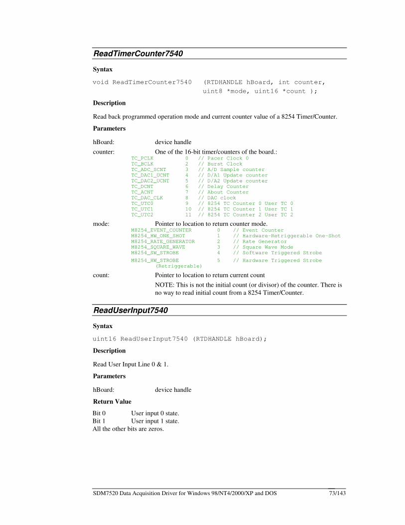
SDM7520 Data Acquisition Driver for Windows 98/NT4/2000/XP and DOS 73/143
ReadTimerCounter7540
Syntax
void ReadTimerCounter7540 (RTDHANDLE hBoard, int counter,
uint8 *mode, uint16 *count );
Description
Read back programmed operation mode and current counter value of a 8254 Timer/Counter.
Parameters
hBoard: device handle counter: One of the 16-bit timer/counters of the board.:
TC_PCLK 0 // Pacer Clock 0 TC_BCLK 2 // Burst Clock TC_ADC_SCNT 3 // A/D Sample counter TC_DAC1_UCNT 4 // D/A1 Update counter TC_DAC2_UCNT 5 // D/A2 Update counter TC_DCNT 6 // Delay Counter TC_ACNT 7 // About Counter TC_DAC_CLK 8 // DAC clock TC_UTC0 9 // 8254 TC Counter 0 User TC 0 TC_UTC1 10 // 8254 TC Counter 1 User TC 1 TC_UTC2 11 // 8254 TC Counter 2 User TC 2
mode: Pointer to location to return counter mode. M8254_EVENT_COUNTER 0 // Event Counter M8254_HW_ONE_SHOT 1 // Hardware-Retriggerable One-Shot M8254_RATE_GENERATOR 2 // Rate Generator M8254_SQUARE_WAVE 3 // Square Wave Mode M8254_SW_STROBE 4 // Software Triggered Strobe
M8254_HW_STROBE 5 // Hardware Triggered Strobe (Retriggerable)
count: Pointer to location to return current count NOTE: This is not the initial count (or divisor) of the counter. There is
no way to read initial count from a 8254 Timer/Counter.
ReadUserInput7540
Syntax
uint16 ReadUserInput7540 (RTDHANDLE hBoard);
Description
Read User Input Line 0 & 1.
Parameters
hBoard: device handle
Return Value
Bit 0 User input 0 state. Bit 1 User input 1 state. All the other bits are zeros.
SDM7520 Data Acquisition Driver for Windows 98/NT4/2000/XP and DOS 74/143
RemoveIRQHandler7540
Syntax
void RemoveIRQHandler7540 (RTDHANDLE hBoard);
Description
This routine is used to uninstall the IRQ handler function.
NOTE: As a side effect, this function disables all interrupt sources enabled when the interrupt handler was installed.
Parameters
hBoard: device handle
ResetCGT7540
Syntax
void ResetCGT7540 (RTDHANDLE hBoard);
Description
Reset the A/D Channel Gain Table pointer to the beginning of the table. After calling this function, the next channel sampled is that of specified by the first entry in the Channel-Gain Table.
NOTE: Calling this function will cause a Channel-Gain Table Reset event. Consider this if you have a sample counter (A/D Sample Counter or the About Counter) configured to count these events or you enabled this event to be an interrupt source.
Parameters
hBoard: device handle
See Also
Channel-Gain Circuitry
ResetDAC1Fifo7540 ResetDAC2Fifo7540
Syntax
void ResetDAC1Fifo7540 (RTDHANDLE hBoard);
void ResetDAC2Fifo7540 (RTDHANDLE hBoard);
Description
Reset the DAC1/DAC2 update pointer to the beginning of the FIFO. After calling this function, the next value output on the D/A converter is the first value in the FIFO, i.e., the one, which was entered first in the FIFO.
SDM7520 Data Acquisition Driver for Windows 98/NT4/2000/XP and DOS 75/143
Parameters
hBoard: device handle
ResetDMA0State7540 ResetDMA1State7540
Syntax
void ResetDMA0State7540 ( RTDHANDLE hBoard );
void ResetDMA1State7540 ( RTDHANDLE hBoard );
Description
Reset DMA state machine (enable next cycle). The function is used in demand mode DMA operation.
Parameters
hBoard: device handle

SDM7520 Data Acquisition Driver for Windows 98/NT4/2000/XP and DOS 77/143
S
SelectDIO0Register7540
Syntax
void SelectDIO0Register7540 ( RTDHANDLE hBoard, int src );
Description
Program digital control register.
Parameters
hBoard: device handle
aReg: 0 - Clear Command
1 - Direction Register
2 - Mask Register
3 - Compare Register
SelectBurstClockPrimaryClock7540
Syntax
void SelectBurstClockPrimaryClock7540 ( RTDHANDLE hBoard, uint16 src );
Description
Select burst clock primary clock frequency.
Parameters
hBoard: device handle
src: CLOCK_8MHZ 0x0 = 8 MHz
CLOCK_20MHZ 0x1 = 20 MHz
SelectDACClockPrimaryClock7540
Syntax
void SelectDACClockPrimaryClock7540 ( RTDHANDLE hBoard, uint16 src );
Description
Select DAC clock primary clock frequency.
Parameters
hBoard: device handle
SDM7520 Data Acquisition Driver for Windows 98/NT4/2000/XP and DOS 78/143
src: CLOCK_8MHZ 0x0 = 8 MHz
CLOCK_20MHZ 0x1 = 20 MHz
SelectPacerClockPrimaryClock7540
Syntax
void SelectPacerClockPrimaryClock7540 ( RTDHANDLE hBoard, uint16 src );
Description
Select pacer clock primary clock frequency.
Parameters
hBoard: device handle
src: CLOCK_8MHZ 0x0 = 8 MHz
CLOCK_20MHZ 0x1 = 20 MHz
Set8254Divisor7540
Syntax
void Set8254Divisor7540 (RTDHANDLE hBoard, int counter,
uint16 divisor);
Description
Load an initial count in a Timer/Counter .
Parameters
hBoard: device handle counter: One of the 16-bit timer/counters of the board.
TC_PCLK 0 // Pacer Clock 0 TC_BCLK 2 // Burst Clock TC_ADC_SCNT 3 // A/D Sample counter TC_DAC1_UCNT 4 // D/A1 Update counter TC_DAC2_UCNT 5 // D/A2 Update counter TC_DCNT 6 // Delay Counter TC_ACNT 7 // About Counter TC_DAC_CLK 8 // DAC clock TC_UTC0 9 // 8254 TC Counter 0 User TC 0 TC_UTC1 10 // 8254 TC Counter 1 User TC 1
TC_UTC2 11 // 8254 TC Counter 2 User TC 2
divisor: 16-bit divisor to divide clock input frequency.
See Also
Timer/Counters
SDM7520 Data Acquisition Driver for Windows 98/NT4/2000/XP and DOS 79/143
Set8254Mode7540
Syntax
void Set8254Mode7540 (RTDHANDLE hBoard, int counter,
uint8 mode);
Description
Sets operating mode of a user timer/counter.
Parameters
hBoard: device handle counter: One of the 16-bit timer/counters of the board.
TC_PCLK 0 // Pacer Clock 0 TC_BCLK 2 // Burst Clock TC_ADC_SCNT 3 // A/D Sample counter TC_DAC1_UCNT 4 // D/A1 Update counter TC_DAC2_UCNT 5 // D/A2 Update counter TC_DCNT 6 // Delay Counter TC_ACNT 7 // About Counter TC_DAC_CLK 8 // DAC clock TC_UTC0 9 // 8254 TC Counter 0 User TC 0 TC_UTC1 10 // 8254 TC Counter 1 User TC 1
TC_UTC2 11 // 8254 TC Counter 2 User TC 2
mode One of the 6 8254 operation modes. M8254_EVENT_COUNTER 0 // Event Counter M8254_HW_ONE_SHOT 1 // Hardware-Retriggerable One-Shot M8254_RATE_GENERATOR 2 // Rate Generator M8254_SQUARE_WAVE 3 // Square Wave Mode M8254_SW_STROBE 4 // Software Triggered Strobe
M8254_HW_STROBE 5 // Hardware Triggered Strobe (Retriggerable)
SetAdcntSource7540
Syntax
void SetAdcntSource7540 (RTDHANDLE hBoard, uint16 src);
Description
Select A/D Sample Counter source.
Parameters
hBoard: device handle src: Use ADC_SCNT_XXXX for argument 'src': ADC_SCNT_CGT_RESET (0)
Count Channel Gain Table resets. Counter counts down by one when the Channel-Gain table turns over to the first table entry.
ADC_SCNT_FIFO_WRITE (1) Count A/D FIFO writes. Counter counts down by one when a new sample is entered in the FIFO.
SDM7520 Data Acquisition Driver for Windows 98/NT4/2000/XP and DOS 80/143
SetBurstRate7540
Syntax
void SetBurstRate7540 ( RTDHANDLE hBoard, float rate,
int clock );
Description
Program the burst clock rate. This is a deprecated function for legacy compatibility. Use the SetBurstRateF7540 function.
Parameters
hBoard: device handle rate: Frequency value (Hertz) between 122Hz and 1,25MHz. clock: Burst Clock Primary Clock Frequency select
CLOCK_8MHZ 0x0 = 8 MHz
CLOCK_20MHZ 0x1 = 20 MHz
SetBurstRateF7540
Syntax
float SetBurstRateF7540 ( RTDHANDLE hBoard, float rate, int clock );
Description
Program the burst clock rate. This function sets the rate by calculating a divisor of the Primary Clock (that equals either 8 MHz or 20 MHz). Since this divisor is rounded to an integer value, the actual burst clock frequency can be different from ‘rate’ parameter.
Parameters
hBoard: device handle rate: Frequency value (Hertz) between 122Hz and 1,25MHz. clock: Burst Clock Primary Clock Frequency select
CLOCK_8MHZ 0x0 = 8 MHz
CLOCK_20MHZ 0x1 = 20 MHz
Return Value
The actual Burst Clock rate.
SetBurstStart7540
Syntax
void SetBurstStart7540 (RTDHANDLE hBoard, uint16 src, int clock);
SDM7520 Data Acquisition Driver for Windows 98/NT4/2000/XP and DOS 81/143
Description
Select Burst Clock start trigger.
NOTE: There is no programmable stop trigger for the Burst Clock. The Burst Clock automatically stops when the Channel-Gain Table resets to its first entry.
Parameters
hBoard: device handle src: Use BCLK_START_XXXX for argument 'src'.
BCLK_START_SOFTWARE 0x0 // Software A/D Start (StartBurst7540) BCLK_START_PCLK 0x1 // Pacer Clock BCLK_START_ETRIG 0x2 // External Trigger BCLK_START_DIGITAL_IT 0x3 // Digital Interrupt BCLK_START_SBUS0 0x4 // SyncBus 0 BCLK_START_SBUS1 0x5 // SyncBus 1
BCLK_START_SBUS2 0x6 // SyncBus 2
Clock: CLOCK_8MHZ 0x0
CLOCK_20MHZ 0x1
See Also
Channel-Gain Circuitry
SetChannelGain7540
Syntax
void SetChannelGain7540 (RTDHANDLE hBoard, uint16 Channel,uint16 Gain, uint16 Range, uint16 Se_Diff, uint16 NrSe );
Description
This routine loads the channel/gain latch.
Parameters
hBoard: device handle Channel: One of the 16 Analog Input channels (0 – AIN1, 1 – AIN2, etc.). Gain: Gain value to apply on the Analog Input channel.
GAIN1 0 GAIN2 1 GAIN4 2 GAIN8 3 GAIN16 4 GAIN32 5
GAIN64 6
Range: Analog Input range. AIN_BIP5 0 // -5..+5 Volt AIN_BIP10 1 // -10..+10 Volt
AIN_UNIP10 2 // 0..+10 Volt Se_Diff: Analog Input channel type:
_GND_SE 0 // Single-Ended
_GND_DIFF 1 // Differential
NrSe: Referencing mode:
SDM7520 Data Acquisition Driver for Windows 98/NT4/2000/XP and DOS 82/143
NRSE_AGND 0 // AGND referenced SE input
NRSE_AINS 1 // AIN SENSE referenced SE input
SetConversionSelect7540
Syntax
void SetConversionSelect7540 (RTDHANDLE hBoard, uint16 Select);
Description
Select A/D Conversion start signal.
Parameters
hBoard: device handle Select:
ADC_START_SOFTWARE 0x0 // Software A/D Start ADC_START_PCLK 0x1 // Pacer Clock (Ext. Int. see Func.509) ADC_START_BCLK 0x2 // Burst Clock ADC_START_DIGITAL_IT 0x3 // Digital Interrupt ADC_START_DAC1_MARKER1 0x4 // D/A 1 Data Marker 1 ADC_START_DAC2_MARKER1 0x5 // D/A 2 Data Marker 1 ADC_START_SBUS0 0x6 // SyncBus 0 ADC_START_SBUS1 0x7 // SyncBus 1
ADC_START_SBUS2 0x8 // SyncBus 2
SetDAC1Cycle7540 SetDAC2Cycle7540
Syntax
void SetDAC1Cycle7540 (RTDHANDLE hBoard, uint16 cycle);
void SetDAC2Cycle7540 (RTDHANDLE hBoard, uint16 cycle);
Description
Program D/A1 or D/A2 Cycle Mode. By setting cycle mode, D/A will continuously output data from the D/A FIFO. When the Update Pointer reaches the end of the FIFO, it resets to the beginning of the FIFO. This mode can be used for generating periodic signals (i.e., waveform generation) without any processor intervention. No cycle mode is the normal (default) mode of operation.
Parameters
hBoard: device handle cycle: 0x0 = no cycle 0x1 = cycle
SetDAC1Range7540 SetDAC2Range7540
Syntax
void SetDAC1Range7540 (RTDHANDLE hBoard, uint16 rng);
void SetDAC2Range7540 (RTDHANDLE hBoard, uint16 rng);
SDM7520 Data Acquisition Driver for Windows 98/NT4/2000/XP and DOS 83/143
Description
Program D/A 1 or D/A 2 output range.
Parameters
hBoard: device handle rng: DAC_UNIPOLAR5 0x0
DAC_UNIPOLAR10 0x1 DAC_BIPOLAR5 0x2
DAC_BIPOLAR10 0x3
SetDAC1Updatet7540 SetDAC2Start7540
Syntax
void SetDAC1Start7540 (RTDHANDLE hBoard, uint16 src);
void SetDAC2Start7540 (RTDHANDLE hBoard, uint16 src);
Description
Select D/A 1 or D/A 2 update signal.
Parameters
hBoard: device handle src:
DAC_START_SOFTWARE 0x0
DAC1/DAC2 Update initiated by a call to UpdateDAC17540/UpdateDAC27540 or UpdateAllDAC7540.
DAC_START_CGT 0x1
= CGT controlled DAC1/DAC2 Update
If the D12 (D13 for D/A2) bit of a Channel-Gain Table entry is set, D/A1 (D/A2) is updated simultaneously with the sampling of the Analog Input channel defined by the entry.
DAC_START_DAC_CLK 0x2
D/A updates are triggered by the dedicated D/A Clock.
DAC_START_EPCLK 0x3
D/A updates are triggered by the External Pacer Clock.
External Clock must produce 100ns pulses, at least. Update occurs on the rising edge.
NOTE: External Pacer Clock can be used independently from the Pacer Clock if Pacer Clock source is programmed to Internal. External Pacer Clock is only a pin on the I/O connector that you may use to for input to the Pacer Clock circuitry.
DAC_START_SBUS0 0x4
DAC_START_SBUS1 0x5
DAC_START_SBUS2 0x6
D/A update started on a rising edge on Synchron Bus line 0/1/2.
SDM7520 Data Acquisition Driver for Windows 98/NT4/2000/XP and DOS 84/143
SetDACDivisor7540 (Windows Only)
Syntax
void SetDACDivisor7540 (RTDHANDLE hBoard, uint32 divisor);
Description
Load the 24 bit wide DAC clock divisor value The 8 MHz input clock frequency is divided with this value generating the output signal. Use of this function is not recommended. Use the SetDACRate function instead. NOTE: The DAC clock starts immediately after loading the divisor. When the start/stop mode is selected, it remains in started state until a stop command is performed. Thus in start/stop mode after programming the DAC clock divisor, a stop command must be performed.
Parameters
hBoard: device handle divisor: divisor value
SetDACRate7540
Syntax
void SetDACRate7540 (RTDHANDLE hBoard, float rate,
int clock);
Description
Setup the D/A clock rate. If the argument clock = 0, the 8 MHz primary clock will be selected for the DAC clock, is clock = 1 the 20 MHz primary clock selected.
Parameters
hBoard: device handle rate: clock rate to setup clock: DAC Clock Primary Clock Frequency select
CLOCK_8MHZ 0x0
CLOCK_20MHZ 0x1
SetDACRateF7540
Syntax
float SetDACRate7540 (RTDHANDLE hBoard, float rate,
int clock);
SDM7520 Data Acquisition Driver for Windows 98/NT4/2000/XP and DOS 85/143
Description
Setup the D/A clock rate. If the argument clock = 0, the 8 MHz primary clock will be selected for the DAC clock, is clock = 1 the 20 MHz primary clock selected.
Parameters
hBoard: device handle rate: clock rate to setup clock: DAC Clock Primary Clock Frequency select
CLOCK_8MHZ 0x0
CLOCK_20MHZ 0x1
Return Value
The actual DAC Clock rate.
SetDIO0Clock7540
Syntax
void SetDIO0Clock7540 (RTDHANDLE hBoard, uint8 src);
Description
Select clock for the Advanced Digital Trigger.
Parameters
hBoard: device handle src: 0 - 8 MHz On-board Oscillator 1 - User TC Counter 1
See Also
Advanced Digital Trigger
SetDIO0CompareMode7540
Syntax
void SetDIO0CompareMode7540 (RTDHANDLE hBoard, uint8 mode);
Description
Programs port 0 compare mode. This register is used for the Advanced Digital Interrupt modes.
Parameters
hBoard: device handle mode: 0 - Event Mode 1 - Match Mode
See Also
Advanced Digital Trigger
SDM7520 Data Acquisition Driver for Windows 98/NT4/2000/XP and DOS 86/143
SetDIO0CompareValue7540
Syntax
void SetDIO0CompareValue7540 (RTDHANDLE hBoard, uint8 compare);
Description
Program Port 0 compare value. Pattern of Port 0 I/O lines for Digital Interrupt generation.
Parameters
hBoard: device handle compare: compare value
See Also
Advanced Digital Trigger
SetDIO0Direction7540
Syntax
void SetDIO0Direction7540 (RTDHANDLE hBoard, uint8 direction);
Description
Program Port 0 direction (bit programmable).
Parameters
hBoard: device handle direction: bit=0 - input bit=1 - output
SetDIO0Mask7540
Syntax
void SetDIO0Mask7540 (RTDHANDLE hBoard, uint8 mask);
Description
Program Digital Interrupt mask for Port 0 I/O lines.
Parameters
hBoard: device handle mask: bit mask to enable/disable I/O lines taking part in Digital Interrupt
generation.
See Also
Advanced Digital Trigger
SDM7520 Data Acquisition Driver for Windows 98/NT4/2000/XP and DOS 87/143
SetDIO1Direction7540
Syntax
void SetDIO1Direction7540 (RTDHANDLE hBoard, uint8 direction);
Description
Program Port 1 direction (byte programmable).
Parameters
hBoard: device handle direction: 0 - input 1 - output
SetEintPolarity7540
Syntax
void SetEintPolarity7540 (RTDHANDLE hBoard, uint16 polarity);
Description
Select External Interrupt polarity.
Parameters
hBoard: device handle polarity: 0x0 = Interrupts are generated on the positive edge of the External
Interrupt line. 0x1 = Interrupts are generated on the negative edge of the External
Interrupt line.
SetEtrgPolarity7540
Syntax
void SetEtrgPolarity7540 (RTDHANDLE hBoard, uint16 polarity);
Description
Select External Trigger polarity.
NOTE: External Trigger polarity also defines the behavior of the Pacer Clock in Gated mode.
Parameters
hBoard: device handle polarity: 0x0 = External Trigger occurs on the positive edge of the External
Trigger line. 0x1 = External Trigger occurs on the negative edge of the External
Trigger line.
SDM7520 Data Acquisition Driver for Windows 98/NT4/2000/XP and DOS 88/143
SetFirstDescriptorBlock7540 (Windows Only)
Syntax
BOOL SetFirstDescriptorBlock7540(RTDHANDLE hBoard, int dma_channel,uint32 dma_local,uint32 direction,uint32 offset, uint32 length);
Description
Setup the first chained mode descriptor block. The first descriptor block starts at the beginning of the allocated DMA buffer in case of channel 0, and at the address of the allocated DMA buffer+0x100. The length of one descriptor block element is 16 bytes, the maximal length of the chaining table is 0x100 bytes for both channel.
Parameters
hBoard: device handle dma_channel: DMA channel index (0/1) dma_local: local (onboard) DMA source/destination direction: transfer direction offset: the offset from the DMA buffer+0x200 address.
the DMA transfer starts from/to here length: DMA transfer length in bytes
Return Value
TRUE If there is no error. FALSE If there is an error.
SDM7520 Data Acquisition Driver for Windows 98/NT4/2000/XP and DOS 89/143
SetFirstDirectDescriptorBlock7540 (Windows Only)
Syntax
BOOL SetFirstDirectDescriptorBlock7540(RTDHANDLE hBoard, int dma_channel,uint32 dma_local, uint32 direction,uint32 direct_address, uint32 length);
Description
Setup the first chained mode descriptor block with direct physical target address.
Starting a DMA cycle to improper address may hangup your system!
Parameters
hBoard: device handle
dma_channel: DMA channel index (0/1)
dma_local: local DMA source/destination address
direction: direction
direct_address: physical DMA address
length: DMA transfer byte count
Return Value
TRUE If there is no error. FALSE If there is an error.
SetHdinStart7540
Syntax
void SetHdinStart7540 (RTDHANDLE hBoard, uint16 src);
Description
Select sampling signal for High Speed Digital Input.
Parameters
hBoard: device handle src: HDIN_SOFTWARE 0x0 // Software Trigger
HDIN_ADC 0x1 // A/D Conversion Signal HDIN_UTC0 0x2 // User TC out 0 HDIN_UTC1 0x3 // User TC out 1 HDIN_UTC2 0x4 // User TC out 2 HDIN_EPCLK 0x5 // External Pacer Clock
HDIN_ETRG 0x6 // External Trigger
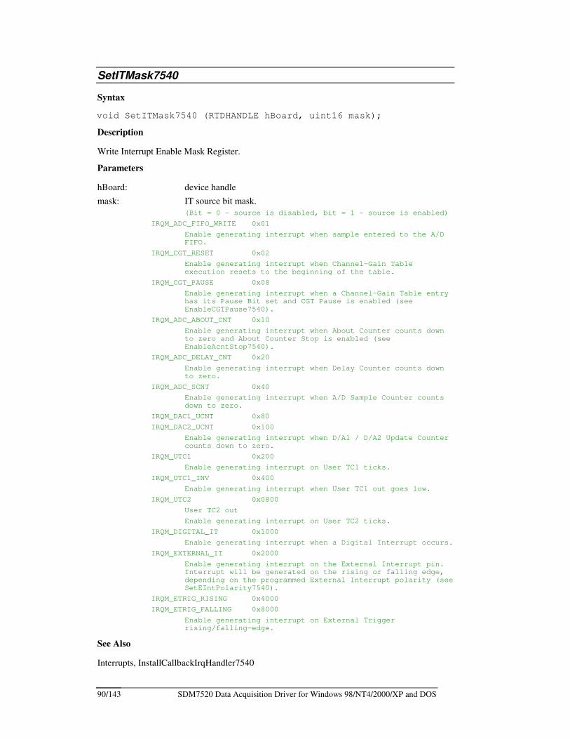
SDM7520 Data Acquisition Driver for Windows 98/NT4/2000/XP and DOS 90/143
SetITMask7540
Syntax
void SetITMask7540 (RTDHANDLE hBoard, uint16 mask);
Description
Write Interrupt Enable Mask Register.
Parameters
hBoard: device handle mask: IT source bit mask. (Bit = 0 - source is disabled, bit = 1 – source is enabled)
IRQM_ADC_FIFO_WRITE 0x01
Enable generating interrupt when sample entered to the A/D FIFO.
IRQM_CGT_RESET 0x02
Enable generating interrupt when Channel-Gain Table execution resets to the beginning of the table.
IRQM_CGT_PAUSE 0x08
Enable generating interrupt when a Channel-Gain Table entry has its Pause Bit set and CGT Pause is enabled (see EnableCGTPause7540).
IRQM_ADC_ABOUT_CNT 0x10
Enable generating interrupt when About Counter counts down to zero and About Counter Stop is enabled (see EnableAcntStop7540).
IRQM_ADC_DELAY_CNT 0x20
Enable generating interrupt when Delay Counter counts down to zero.
IRQM_ADC_SCNT 0x40
Enable generating interrupt when A/D Sample Counter counts down to zero.
IRQM_DAC1_UCNT 0x80
IRQM_DAC2_UCNT 0x100
Enable generating interrupt when D/A1 / D/A2 Update Counter counts down to zero.
IRQM_UTC1 0x200
Enable generating interrupt on User TC1 ticks.
IRQM_UTC1_INV 0x400
Enable generating interrupt when User TC1 out goes low.
IRQM_UTC2 0x0800
User TC2 out
Enable generating interrupt on User TC2 ticks.
IRQM_DIGITAL_IT 0x1000
Enable generating interrupt when a Digital Interrupt occurs.
IRQM_EXTERNAL_IT 0x2000
Enable generating interrupt on the External Interrupt pin. Interrupt will be generated on the rising or falling edge, depending on the programmed External Interrupt polarity (see SetEIntPolarity7540).
IRQM_ETRIG_RISING 0x4000
IRQM_ETRIG_FALLING 0x8000
Enable generating interrupt on External Trigger rising/falling-edge.
See Also
Interrupts, InstallCallbackIrqHandler7540
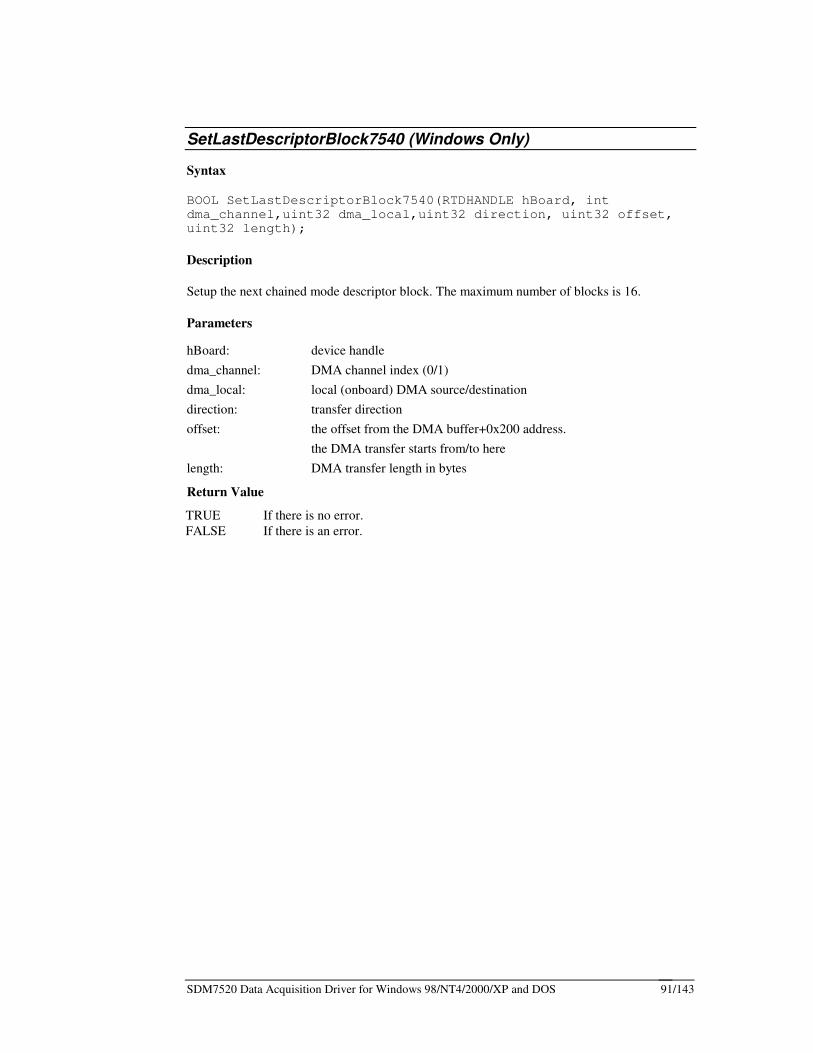
SDM7520 Data Acquisition Driver for Windows 98/NT4/2000/XP and DOS 91/143
SetLastDescriptorBlock7540 (Windows Only)
Syntax
BOOL SetLastDescriptorBlock7540(RTDHANDLE hBoard, int dma_channel,uint32 dma_local,uint32 direction, uint32 offset, uint32 length);
Description
Setup the next chained mode descriptor block. The maximum number of blocks is 16.
Parameters
hBoard: device handle dma_channel: DMA channel index (0/1) dma_local: local (onboard) DMA source/destination direction: transfer direction offset: the offset from the DMA buffer+0x200 address.
the DMA transfer starts from/to here length: DMA transfer length in bytes
Return Value
TRUE If there is no error. FALSE If there is an error.
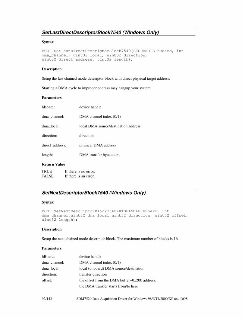
SDM7520 Data Acquisition Driver for Windows 98/NT4/2000/XP and DOS 92/143
SetLastDirectDescriptorBlock7540 (Windows Only)
Syntax
BOOL SetLastDirectDescriptorBlock7540(RTDHANDLE hBoard, int dma_channel, uint32 local, uint32 direction, uint32 direct_address, uint32 length);
Description
Setup the last chained mode descriptor block with direct physical target address.
Starting a DMA cycle to improper address may hangup your system!
Parameters
hBoard: device handle
dma_channel: DMA channel index (0/1)
dma_local: local DMA source/destination address
direction: direction
direct_address: physical DMA address
length: DMA transfer byte count
Return Value
TRUE If there is no error. FALSE If there is an error.
SetNextDescriptorBlock7540 (Windows Only)
Syntax
BOOL SetNextDescriptorBlock7540(RTDHANDLE hBoard, int dma_channel,uint32 dma_local,uint32 direction, uint32 offset, uint32 length);
Description
Setup the next chained mode descriptor block. The maximum number of blocks is 16.
Parameters
hBoard: device handle dma_channel: DMA channel index (0/1) dma_local: local (onboard) DMA source/destination direction: transfer direction offset: the offset from the DMA buffer+0x200 address.
the DMA transfer starts from/to here
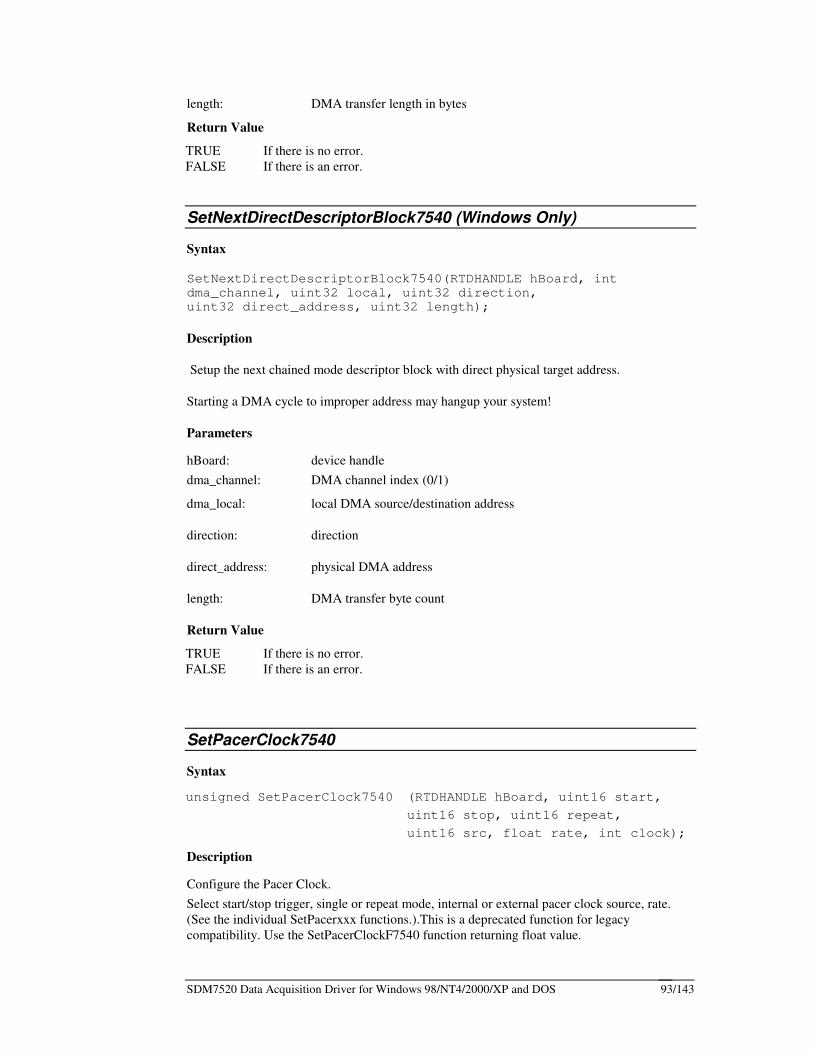
SDM7520 Data Acquisition Driver for Windows 98/NT4/2000/XP and DOS 93/143
length: DMA transfer length in bytes
Return Value
TRUE If there is no error. FALSE If there is an error.
SetNextDirectDescriptorBlock7540 (Windows Only)
Syntax
SetNextDirectDescriptorBlock7540(RTDHANDLE hBoard, int dma_channel, uint32 local, uint32 direction, uint32 direct_address, uint32 length);
Description
Setup the next chained mode descriptor block with direct physical target address.
Starting a DMA cycle to improper address may hangup your system!
Parameters
hBoard: device handle dma_channel: DMA channel index (0/1)
dma_local: local DMA source/destination address
direction: direction
direct_address: physical DMA address
length: DMA transfer byte count
Return Value
TRUE If there is no error. FALSE If there is an error.
SetPacerClock7540
Syntax
unsigned SetPacerClock7540 (RTDHANDLE hBoard, uint16 start,
uint16 stop, uint16 repeat,
uint16 src, float rate, int clock);
Description
Configure the Pacer Clock. Select start/stop trigger, single or repeat mode, internal or external pacer clock source, rate. (See the individual SetPacerxxx functions.).This is a deprecated function for legacy compatibility. Use the SetPacerClockF7540 function returning float value.
SDM7520 Data Acquisition Driver for Windows 98/NT4/2000/XP and DOS 94/143
Parameters
hBoard: device handle start: Pacer Start trigger
PCLK_START_SOFTWARE 0x0 // Software Pacer Start (StartPacer7540) PCLK_START_ETRIG 0x1 // External trigger PCLK_START_DIGITAL_IT 0x2 // Digital interrupt PCLK_START_UTC2 0x3 // User TC 2 out PCLK_START_SBUS0 0x4 // SyncBus 0 PCLK_START_SBUS1 0x5 // SyncBus 1 PCLK_START_SBUS2 0x6 // SyncBus 2 PCLK_START_D_SOFTWARE 0x8 // Delayed Software Pacer Start PCLK_START_D_ETRIG 0x9 // Delayed external trigger PCLK_START_D_DIGITAL_IT 0xA // Delayed digital interrupt PCLK_START_D_UTC2 0xB // Delayed User TC 2 out PCLK_START_D_SBUS0 0xC // Delayed SyncBus 0 PCLK_START_D_SBUS1 0xD // Delayed SyncBus 1 PCLK_START_D_SBUS2 0xE // Delayed SyncBus 2
PCLK_START_ETRIG_GATED 0xF // External Trigger Gated controlled mode
stop: Pacer Stop trigger PCLK_STOP_SOFTWARE 0x0 // Software Pacer Stop (StopPacer7540) PCLK_STOP_ETRIG 0x1 // External Trigger PCLK_STOP_DIGITAL_IT 0x2 // Digital Interrupt PCLK_STOP_ACNT 0x3 // About Counter PCLK_STOP_UTC2 0x4 // User TC2 out PCLK_STOP_SBUS0 0x5 // SyncBus 0 PCLK_STOP_SBUS1 0x6 // SyncBus 1 PCLK_STOP_SBUS2 0x7 // SyncBus 2 PCLK_STOP_A_SOFTWARE 0x8 // About Software Pacer Stop PCLK_STOP_A_ETRIG 0x9 // About External Trigger PCLK_STOP_A_DIGITAL_IT 0xA // About Digital Interrupt PCLK_STOP_A_UTC2 0xC // About User TC2 out PCLK_STOP_A_SBUS0 0xD // About SyncBus 0 PCLK_STOP_A_SBUS1 0xE // About SyncBus 1
PLK_STOP_A_SBUS2 0xF // About SyncBus 2
repeat: Pacer Clock retriggering mode PLK_NO_REPEAT 0x0 = Single Cycle Mode - new cycle is
ossible after a Software Pacer Start command
PCLK_REPEAT 0x1 = Trigger Repeat Mode - Pacer can be started by the selected Pacer Start Trigger
src: Pacer Clock select PCLK_INTERNAL 1 // Internal Pacer Clock
PCLK_EXTERNAL 0 // External Pacer Clock
rate: Pacer Clock rate in Hertz. Ignored if Pacer Clock source (src) is External Pacer Clock.
clock: Pacer Clock Primary Clock Frequency select CLOCK_8MHZ 0x0
CLOCK_20MHZ 0x1
Return Value
The actual pacer rate set by the function. This value could be different from the requested rate if the rate divisor does not divide the selected clock evenly.
SetPacerClockF7540
Syntax
float SetPacerClockF7540 (RTDHANDLE hBoard, uint16 start,
uint16 stop, uint16 repeat,
SDM7520 Data Acquisition Driver for Windows 98/NT4/2000/XP and DOS 95/143
uint16 src, float rate, int clock);
Description
Configure the Pacer Clock. Select start/stop trigger, single or repeat mode, internal or external pacer clock source, rate. (See the individual SetPacerxxx functions.)
Parameters
hBoard: device handle start: Pacer Start trigger
PCLK_START_SOFTWARE 0x0 // Software Pacer Start (StartPacer7540) PCLK_START_ETRIG 0x1 // External trigger PCLK_START_DIGITAL_IT 0x2 // Digital interrupt PCLK_START_UTC2 0x3 // User TC 2 out PCLK_START_SBUS0 0x4 // SyncBus 0 PCLK_START_SBUS1 0x5 // SyncBus 1 PCLK_START_SBUS2 0x6 // SyncBus 2 PCLK_START_D_SOFTWARE 0x8 // Delayed Software Pacer Start PCLK_START_D_ETRIG 0x9 // Delayed external trigger PCLK_START_D_DIGITAL_IT 0xA // Delayed digital interrupt PCLK_START_D_UTC2 0xB // Delayed User TC 2 out PCLK_START_D_SBUS0 0xC // Delayed SyncBus 0 PCLK_START_D_SBUS1 0xD // Delayed SyncBus 1 PCLK_START_D_SBUS2 0xE // Delayed SyncBus 2
PCLK_START_ETRIG_GATED 0xF // External Trigger Gated controlled stop: Pacer Stop trigger
PCLK_STOP_SOFTWARE 0x0 // Software Pacer Stop (StopPacer7540) PCLK_STOP_ETRIG 0x1 // External Trigger PCLK_STOP_DIGITAL_IT 0x2 // Digital Interrupt PCLK_STOP_ACNT 0x3 // About Counter PCLK_STOP_UTC2 0x4 // User TC2 out PCLK_STOP_SBUS0 0x5 // SyncBus 0 PCLK_STOP_SBUS1 0x6 // SyncBus 1 PCLK_STOP_SBUS2 0x7 // SyncBus 2 PCLK_STOP_A_SOFTWARE 0x8 // About Software Pacer Stop PCLK_STOP_A_ETRIG 0x9 // About External Trigger PCLK_STOP_A_DIGITAL_IT 0xA // About Digital Interrupt PCLK_STOP_A_UTC2 0xC // About User TC2 out PCLK_STOP_A_SBUS0 0xD // About SyncBus 0 PCLK_STOP_A_SBUS1 0xE // About SyncBus 1
PLK_STOP_A_SBUS2 0xF // About SyncBus 2 repeat: Pacer Clock retriggering mode
PLK_NO_REPEAT 0x0 = Single Cycle Mode - new cycle is ossible after a Software Pacer Start command
PCLK_REPEAT 0x1 = Trigger Repeat Mode - Pacer can be started by the selected Pacer Start Trigger
src: Pacer Clock select PCLK_INTERNAL 1 // Internal Pacer Clock
PCLK_EXTERNAL 0 // External Pacer Clock rate: Pacer Clock rate in Hertz. Ignored if Pacer Clock source (src) is
External Pacer Clock. clock: Pacer Clock Primary Clock Frequency select
CLOCK_8MHZ 0x0
CLOCK_20MHZ 0x1
Return Value
The actual pacer rate set by the function. This value could be different from the requested rate if the rate divisor does not divide the selected clock evenly.
SDM7520 Data Acquisition Driver for Windows 98/NT4/2000/XP and DOS 96/143
SetPacerRate7540
Syntax
unsigned SetPacerRate7540 ( RTDHANDLE hBoard, float rate, int clock );
Description
Program Pacer Clock rate. This is a deprecated function for legacy compatibility. Use the SetPacerRateF7540 function.
Parameters
hBoard: device handle rate: Clock frequency (Hertz). Valid values are between 0.0018Hz and
1.25MHz. clock: Pacer Clock Primary Clock Frequency select
CLOCK_8MHZ 0x0
CLOCK_20MHZ 0x1
Return Value
The actual pacer rate set by the function. This value could be different from the requested rate if the rate divisor does not divide the selected clock evenly.
SetPacerRateF7540
Syntax
float SetPacerRateF7540 ( RTDHANDLE hBoard, float rate, int clock );
Description
Program Pacer Clock rate. This function sets the rate by calculating a divisor of the Primary Clock (that equals either 8 MHz or 20 MHz). Since this divisor is rounded to an integer value, the actual pacer clock frequency can be different from ‘rate’ parameter.
Parameters
hBoard: device handle rate: Clock frequency (Hertz). Valid values are between 0.0018Hz and
1.25MHz. clock: Pacer Clock Primary Clock Frequency select
CLOCK_8MHZ 0x0
CLOCK_20MHZ 0x1
Return Value
The actual pacer rate set by the function. This value could be different from the requested rate if the rate divisor does not divide the selected clock evenly.
SetPacerRepeat7540
Syntax
void SetPacerRepeat7540 (RTDHANDLE hBoard, uint16 repeat);
SDM7520 Data Acquisition Driver for Windows 98/NT4/2000/XP and DOS 97/143
Description
Pacer Start Trigger Mode select.
Parameters
hBoard: device handle repeat:
PCLK_NO_REPEAT 0x0 = Single Cycle Mode - new cycle is possible only after a Software Pacer Start command
PCLK_REPEAT 0x1 = Trigger Repeat Mode -paccer can be started by the selected Pacer Start Trigger
SetPacerSource7540
Syntax
void SetPacerSource7540 (RTDHANDLE hBoard, uint16 src);
Description
Select Pacer Clock Source.
Parameters
hBoard: device handle src: PCLK_INTERNAL 1 // Internal Pacer Clock
PCLK_EXTERNAL 0 // External Pacer Clock
SetPacerStart7540
Syntax
void SetPacerStart7540 (RTDHANDLE hBoard, uint16 src);
Description
Select Pacer Clock start trigger.
Parameters
hBoard: device handle PCLK_START_SOFTWARE 0x0
Pacer Clock is started by a call to StartPacer7540.
PCLK_START_ETRIG 0x1
A positive- or negative-going edge (depending on the setting of the trigger polarity, SetEtrgPolarity7540) on the external TRIGGER INPUT line, will start the Pacer Clock. The pulse duration should be at least 100 nanoseconds.
NOTE: If the Pacer Clock is already running when an External Trigger occurs, behavior depends on the programmed Pacer Clock Repeat Mode (see SetPacerRepeat7540).
PCLK_START_DIGITAL_IT 0x2
Pacer Clock is started when a Digital Interrupt occurs.
PCLK_START_UTC2 0x3
Pacer Clock is started by User T/C 2 (when counter reaches 0).
PCLK_START_SBUS0 0x4
PCLK_START_SBUS1 0x5
PCLK_START_SBUS2 0x6
SDM7520 Data Acquisition Driver for Windows 98/NT4/2000/XP and DOS 98/143
Pacer Clock is started by a positive edge of Synchron Bus line 0/1/2, respectively.
PCLK_START_D_SOFTWARE 0x8
PCLK_START_D_ETRIG 0x9
PCLK_START_D_DIGITAL_IT 0xA
PCLK_START_D_UTC2 0xB
PCLK_START_D_SBUS0 0xC
PCLK_START_D_SBUS1 0xD
PCLK_START_D_SBUS2 0xE
These start trigger sources provide delayed triggering (see Pre/Post Triggering).
When the selected trigger occurs, the A/D Delay Counter starts the Pacer Clock, but Pacer Clock is not yet enabled to drive the A/D converter. When the Delay Counter counts down to zero, the Pacer Clock starts driving the A/D converter.
PCLK_START_ETRIG_GATED 0xF
Pacer Clock is started/stopped by the External Trigger line.
In this mode, the External Trigger line serves as the gate of the Pacer Clock. Pacer Clock runs when line goes high and stops when the line goes low, or vice-versa, depending on the programmed External Trigger polarity (see SetEtrgPolarity7540).
In this mode of operation, programming Pacer Clock stop trigger (SetPacerStop7540) has no effect.
SetPacerStop7540
Syntax
void SetPacerStop7540 (RTDHANDLE hBoard, uint16 src);
Description
Select Pacer Clock Stop Trigger.
Parameters
hBoard: device handle src:
PCLK_STOP_SOFTWARE 0x0
Pacer Clock is stopped by a call to StopPacer7540.
PCLK_STOP_ETRIG 0x1
Pacer Clock stops when an External Trigger occurs.
A positive- or negative-going edge (depending on the trigger polarity programmed by SetEtrgPolarity7540) on the external TRIGGER INPUT line, will stop the Pacer Clock. The pulse duration should be at least 100 nanoseconds.
PCLK_STOP_DIGITAL_IT 0x2
Pacer Clock stops when a Digital Interrupt occurs.
PCLK_STOP_ACNT 0x3
Pacer Clock is stopped by the About Counter.
Pacer Clock stops when About Counter counts down to zero and About Counter Stop is enabled (see EnableAcntStop7540). About Counter counts the samples that are actually entering the A/D FIFO
Use this mode for post triggering (see Pre/Post Triggering).
PCLK_STOP_UTC2 0x4
Pacer Clock stops when User T/C2 counts down to zero.
PCLK_STOP_SBUS0 0x5
PCLK_STOP_SBUS1 0x6
SDM7520 Data Acquisition Driver for Windows 98/NT4/2000/XP and DOS 99/143
PCLK_STOP_SBUS2 0x7
Pacer Clock is stopped when a rising edge occurs on Synchron Bus line 0/1/2, respectively.
PCLK_STOP_A_SOFTWARE 0x8
PCLK_STOP_A_ETRIG 0x9
PCLK_STOP_A_DIGITAL_IT 0xA
PCLK_STOP_A_UTC2 0xC
PCLK_STOP_A_SBUS0 0xD
PCLK_STOP_A_SBUS1 0xE
PCLK_STOP_A_SBUS2 0xF
These stop trigger sources are to provide about triggering (see Pre/Port Triggering).
When the selected stop trigger occurs, About Counter starts counting the A/D samples entering the A/D FIFO. When About Counter counts down to zero, it stops the Pacer Clock.
SetPclkSize7540
Syntax
void SetPclkSize7540 (RTDHANDLE hBoard, uint16 size);
Description
This function is deprecated. The pacer clock size is always 24bits on the SDM7540
SetSbus0Source7540
Syntax
void SetSbus0Source7540 (RTDHANDLE hBoard, uint16 src);
Description
Select Synchron Bus line 0 signal.
NOTE: To export a signal to the Synchron Bus it is not enough to set the source by this function. You also have to enable the selected source signal to appear on the bus by calling EnableSBus07540.
Parameters
hBoard: device handle src:
SBUS0_START_ADC_COMMAND 0
Synchron Bus line 0 will be equivalent with the signal caused by the execution of StartConversion7540.
SBUS0_PCLK 1
Put the Out line of the Pacer Clock on the bus.
SBUS0_BCLK 2
Put the Out line of the Burst Clock on the bus.
SBUS0_CGT_DAC1_UPDATE 3
Bus line 0 will be equivalent with the signal of the CGT controlled D/A1 updates.
SBUS0_ETRG 4
Put External Trigger signal on the bus.
SBUS0_START_DACS_COMMAND 5
SDM7520 Data Acquisition Driver for Windows 98/NT4/2000/XP and DOS 100/143
Bus line 0 will be equivalent with the signal caused by a simultaneous D/A1 and D/A2 update by UpdateAllDAC7540.
SBUS0_DAC_CLK 6
Put the Out line of the D/A Clock on the bus.
SBUS0_UTC2 7
Put the Out line of the User TC2 on the bus.
See Also
Synchron Bus
SetSbus1Source7540
Syntax
void SetSbus1Source7540 (RTDHANDLE hBoard, uint16 src);
Description
Select Synchron Bus line 1 signal.
NOTE: To export a signal to the Synchron Bus it is not enough to set the source by this function. You also have to enable the selected source signal to appear on the bus by calling EnableSBus17540.
Parameters
hBoard: device handle src:
SBUS1_START_ADC_COMMAND 0
Synchron Bus line 1 will be equivalent with the signal caused by the execution of StartConversion7540.
SBUS1_PCLK 1
Put the Out line of the Pacer Clock on the bus.
SBUS1_BCLK 2
Put the Out line of the Burst Clock on the bus.
SBUS1_CGT_DAC2_UPDATE 3
Bus line 1 will be equivalent with the signal of the CGT controlled D/A2 updates.
SBUS1_ETRG 4
Put External Trigger signal on the bus.
SBUS1_START_DACS_COMMAND 5
Bus line 1 will be equivalent with the signal caused by a simultaneous D/A1 and D/A2 update by UpdateAllDAC7540.
SBUS1_DAC_CLK 6
Put the Out line of the D/A Clock on the bus.
SBUS1_UTC2 7
Put the Out line of the User TC2 on the bus.
See Also
Synchron Bus
SetSbus2Source7540
Syntax
void SetSbus2Source7540 (RTDHANDLE hBoard, uint16 src);
SDM7520 Data Acquisition Driver for Windows 98/NT4/2000/XP and DOS 101/143
Description
Select Synchron Bus line 2 signal.
NOTE: To export a signal to the Synchron Bus it is not enough to set the source by this function. You also have to enable the selected source signal to appear on the bus by calling EnableSBus27540.
Parameters
hBoard: device handle src:
SBUS2_START_ADC_COMMAND 0
Synchron Bus line 2 will be equivalent with the signal caused by the execution of StartConversion7540.
SBUS2_START_PCLK_COMMAND 1
Synchron Bus line 2 will be equivalent with the signal caused by the execution of StartPacer7540.
SBUS2_STOP_CLK_COMMAND 2
Synchron Bus line 2 will be equivalent with the signal caused by the execution of StopPacer7540.
SBUS2_UPDATE_DAC1 3
SBUS2_UPDATE_DAC2 4
Bus line 2 will be equivalent with the signal caused by a D/A1 and D/A2 update by UpdateDAC17540/UpdateDAC27540.
SBUS2_EPCLK 5
Put External Pacer Clock signal on the bus.
SBUS2_ETRG 6
Put External Trigger signal on the bus.
SBUS1_UTC2 7
Put the Out line of the User TC2 on the bus.
See Also
Synchron Bus
SetUout0Source7540 SetUout1Source7540
Syntax
void SetUout0Source7540 (RTDHANDLE hBoard, uint16 src);
void SetUout1Source7540 (RTDHANDLE hBoard, uint16 src);
Description
Select User Output 0/1 signal.
Parameters
hBoard: device handle src:
UOUT_ADC 0x0 // A/D Conversion Signal UOUT_DAC1 0x1 // D/A1 Update UOUT_DAC2 0x2 // D/A2 Update UOUT_SOFTWARE 0x3 // Software Programmable by LAS0+4h
(WriteUserOutput7540)
SDM7520 Data Acquisition Driver for Windows 98/NT4/2000/XP and DOS 102/143
SetupAboutCounter7540
Syntax
void SetupAboutCounter7540 (RTDHANDLE hBoard,
uint16 samples,
uint16 enable );
Description
Program the about counter. The function programs the rate and enables or disables the about counter.
NOTE: This function is a short for the following calls:
Set8254Mode7540(hBoard,TC_ACNT,M8254_RATE_GENERATOR); Set8254Divisor7540(hBoard,TC_ACNT,samples); EnableAcntStop7540(hBoard,enable);
Parameters
hBoard: device handle samples: initial count enable: 1: stop disabled 0: stop enable
SetupBurst7540
Syntax
void SetupBurst7540 (RTDHANDLE hBoard, uint16 start,
float rate, int clock);
Description
Setup the burst clock. This is a deprecated function for legacy compatibility. Please use function SetupBurstF7540.
NOTE: This function is a short for the following calls:
SetBurstStart7540(hBoard,start); SetBurstRate7540(hBoard,rate);
Parameters
hBoard: device handle start: Burst Trigger source. rate: Burst clock rate (in Hertz). clock: Burst Clock Primary Clock Frequency select
CLOCK_8MHZ 0x0
CLOCK_20MHZ 0x1
SDM7520 Data Acquisition Driver for Windows 98/NT4/2000/XP and DOS 103/143
SetupBurstF7540
Syntax
float SetupBurstF7540 (RTDHANDLE hBoard, uint16 start,
float rate, int clock);
Description
Setup the burst clock. (See the SetBurstStart7540 and the SetBurstRateF7540 functions).
NOTE: This function is a short for the following calls:
SetBurstStart7540(hBoard,start); SetBurstRateF7540(hBoard,rate);
Parameters
hBoard: device handle start: Burst Trigger source. rate: Burst clock rate (in Hertz). clock: Burst Clock Primary Clock Frequency select
CLOCK_8MHZ 0x0
CLOCK_20MHZ 0x1
Return Value
The actual Burst Clock rate.
SetupCgtRow7540
Syntax
void SetupCgtRow7540 (ioctrl_t *cscRow,
int aChannel, int aGain, int aRange,
int aNRSE, int aGround, int aPause,
int aDAC1, int aDAC2, int aSkip );
Description
Setup a Channel-Gain Table entry.
Parameters
ioctrl_t *cscRow structure for CGT rows aChannel Analog Input channel to sample (0…15 for AIN1…AIN16). aGain Analog Input gain to apply on the analog
GAIN1 0 GAIN2 1 GAIN4 2 GAIN8 3 GAIN16 4 GAIN32 5
GAIN64 6 aRange Analog Input range:
AIN_BIP5 0 // -5..+5 Volt
SDM7520 Data Acquisition Driver for Windows 98/NT4/2000/XP and DOS 104/143
AIN_BIP10 1 // -10..+10 Volt
AIN_UNIP10 2 // 0..+10 Volt
aNRSE Ground referencing mode: NRSE_AGND 0 // AGND referenced SE input
NRSE_AINS 1 // AIN SENSE referenced SE input
aGround Analog Input Type: _GND_SE 0 // Single-Ended
_GND_DIFF 1 // Differential
aPause Pause Bit CGT_PAUSE_DISABLE 0
CGT_PAUSE_ENABLE 1
aDAC1 ADAC2 D/A1 / D/A2 Update Bit: 0 do not update D/A1 / D/A2
1 update D/A1 / D/A2
aSkip Skip Bit: 0 store converted A/D sample to FIFO
1 discard converted A/D sample
See Also
Channel-Gain Circuitry, WriteCGTAnalog7540
SetupChainedDMA7540 (Windows Only)
Syntax
BOOL SetupChainedDMA7540(RTDHANDLE hBoard, int dma_channel, uint16 demand_source, uint32 mode, BOOL it_enable);
Description
Setup the chained mode DMA operation.
Parameters
hBoard: device handle dma_channel: DMA channel index (0/1) demand_source: source of demand mode DMA request
DMAS_DISABLED 0x0 // DMA Disabled DMAS_ADC_SCNT 0x1 // ADC Sample Counter DMAS_DAC1_UCNT 0x2 // D/A1 Update Counter DMAS_DAC2_UCNT 0x3 // D/A2 Update Counter DMAS_UTC1 0x4 // User TC1 out DMAS_ADFIFO_HALF_FULL 0x8 // A/D FIFO half full DMAS_DAC1_FIFO_HALF_EMPTY 0x9 // D/A1 FIFO half empty
DMAS_DAC2_FIFO_HALF_EMPTY 0xA // D/A2 FIFO half empty
mode: mode DMAMODE0_NORMAL_CHAIN16 DMAMODE0_DEMAND_CHAIN16 DMAMODE0_NORMAL_CHAIN32 DMAMODE0_DEMAND_CHAIN32 - Or - DMAMODE1_NORMAL_CHAIN16 DMAMODE1_DEMAND_CHAIN16 DMAMODE1_NORMAL_CHAIN32
DMAMODE1_DEMAND_CHAIN32
it_enable: enable DMA done interrupt
SDM7520 Data Acquisition Driver for Windows 98/NT4/2000/XP and DOS 105/143
Return Value
TRUE If there is no error. FALSE If there is an error.
SetupDAC7540
Syntax
void SetupDAC7540 (RTDHANDLE hBoard, int idx, uint16 rng, uint16 cycle, uint16 src );
Description
Setup DAC.
NOTE: This function is a short for the following calls:
SetDACXRange7540(hBoard,rng); SetDACXStart7540(hBoard,src); SetDACXCycle7540(hBoard,cycle); Parameters
hBoard: device handle idx:
0: DAC1,
1: DAC2
rng: range DAC_UNIPOLAR5 0x0 DAC_UNIPOLAR10 0x1 DAC_BIPOLAR5 0x2
DAC_BIPOLAR10 0x3
cycle: cycle mode DAC_CYCLE_SINGLE 0x0 // not cycle
DAC_CYCLE_MULTI 0x1 // cycle
src: start source DAC_UPDATE_SOFTWARE 0x0 // Software Update DAC_UPDATE_CGT 0x1 // CGT controlled Update DAC_UPDATE_DAC_CLK 0x2 // D/A Clock DAC_UPDATE_EPCLK 0x3 // External Pacer Clock DAC_UPDATE_SBUS0 0x4 // SyncBus 0 DAC_UPDATE_SBUS1 0x5 // SyncBus 1
DAC_UPDATE_SBUS2 0x6 // SyncBus 2
SetupDelayCounter7540
Syntax
void SetupDelayCounter7540 (RTDHANDLE hBoard, uint16 samples);
Description
Program the delay counter.
Parameters
hBoard: device handle samples: number of samples to delay
SDM7520 Data Acquisition Driver for Windows 98/NT4/2000/XP and DOS 106/143
SetupDirectDMA7540 (Windows Only)
Syntax
BOOL SetupDirectDMA7540(RTDHANDLE hBoard, int dma_channel, uint32 dma_source, uint16 demand_source, uint32 mode, int direction, uint32 direct_address, uint32 length, BOOL it_enable);
Description
Setup DMA channel with direct physical target address.
Starting a DMA cycle to improper address may hangup your system!
Parameters
hBoard: device handle
dma_channel: DMA channel index (0/1)
dma_source: address of DMA data source
demand_source: hardware signal for demand mode DMA DMAS_DISABLED 0x0 // DMA Disabled
DMAS_ADC_SCNT 0x1 // ADC Sample Counter DMAS_DAC1_UCNT 0x2 // D/A1 Update Counter DMAS_DAC2_UCNT 0x3 // D/A2 Update Counter DMAS_UTC1 0x4 // User TC1 out DMAS_ADFIFO_HALF_FULL 0x8 // A/D FIFO half full DMAS_DAC1_FIFO_HALF_EMPTY 0x9 // D/A1 FIFO half empty
DMAS_DAC2_FIFO_HALF_EMPTY 0xA // D/A2 FIFO half empty
mode: DMA mode DMAMODE0_NORMAL DMAMODE0_DEMAND -Or- DMAMODE1_NORMAL
DMAMODE1_DEMAND
direction: data flow direction
DMAD_FROMCARD 1 // DMA transfer from card to memory
DMAD_TOCARD 0 // DMA transfer from memory to card
direct_address: physical address to DMA
length: number of bytes to transfer
enable: DMA done interrupt enable
Return Value
TRUE If there is no error. FALSE If there is an error.
SDM7520 Data Acquisition Driver for Windows 98/NT4/2000/XP and DOS 107/143
SetupDMA7540
Syntax
BOOL SetupDMA7540(RTDHANDLE hBoard, int dma_channel, uint32 dma_source, uint16 demand_source, uint32 mode, int direction, uint32 offset, uint32 length, BOOL it_enable);
Description
Setup DMA channel before start data transfer.
Parameters
hBoard: device handle dma_channel: DMA channel index (0/1) dma_source: address of DMA data source demand_source: hardware signal for demand mode DMA
DMAS_DISABLED 0x0 // DMA Disabled DMAS_ADC_SCNT 0x1 // ADC Sample Counter
DMAS_DAC1_UCNT 0x2 // D/A1 Update Counter DMAS_DAC2_UCNT 0x3 // D/A2 Update Counter DMAS_UTC1 0x4 // User TC1 out DMAS_ADFIFO_HALF_FULL 0x8 // A/D FIFO half full DMAS_DAC1_FIFO_HALF_EMPTY 0x9 // D/A1 FIFO half empty
DMAS_DAC2_FIFO_HALF_EMPTY 0xA // D/A2 FIFO half empty
mode: DMA mode Either: DMAMODE0_NORMAL DMAMODE0_DEMAND DMAMODE0_NORMAL_CHAIN DMAMODE0_DEMAND_CHAIN -Or- DMAMODE1_NORMAL DMAMODE1_DEMAND DMAMODE1_NORMAL_CHAIN
DMAMODE1_DEMAND_CHAIN
direction: data flow direction DMAD_FROMCARD 1 // DMA transfer from card to memory
DMAD_TOCARD 0 // DMA transfer from memory to card
offset: data offset from the beginning of the driver allocated buffer length: number of bytes to transfer enable: DMA done interrupt enable
Return Value
TRUE If there is no error. FALSE If there is an error.
SetupPort07540
Syntax
void SetupPort07540 (RTDHANDLE hBoard, uint8 direction, uint8 mask, uint8 mode, uint8 compare, uint8 clock,BOOL irq );
Description
Configure Digital I/O Port 0.
SDM7520 Data Acquisition Driver for Windows 98/NT4/2000/XP and DOS 108/143
NOTE: This function is a short for the following calls:
SetDIO0Direction7540(hBoard,direction); SetDIO0Mask7540(hBoard,mask); SetDIO0CompareMode7540(hBoard,mode); SetDIO0CompareValue7540(hBoard,compare);
SetDIO0Clock7540(hBoard,clock);
EnableDIO0Irq7540(hBoard,irq);
Parameters
hBoard: device handle direction: 8-bit mask specifying the direction of the individual lines (see
SetDIO0Direction7540) mask: Digital Interrupt generation mask (see SetDIO0Mask7540) mode: Triggering Mode (see SetDIO0CompareMode7540) compare: Compare value for Match mode (see SetDIO0CompareValue7540) clock: Clock for Digital Triggering (see SetDIO0CLock7540) irq: Enable/disable Digital Interrupt generation (see EnableDIO0Irq7540)
SetupPort17540
Syntax
void SetupPort17540 (RTDHANDLE hBoard, uint8 direction);
Description
Configure Digital I/O Port 1.
NOTE: This function is a short for the following calls:
SetDIO1Direction7540(hBoard,direction); Parameters
hBoard: device handle direction: port direction (see SetDIO1Direction7540)
SetupSampleCounter7540
Syntax
void SetupSampleCounter7540 (RTDHANDLE hBoard,
int counter,uint16 src,
uint16 count);
Description
Program one of the 3 sample counters.
NOTE: This function is a short for the following calls:
switch ( counter ) { case TC_ADC_SCNT:
SetAdcntSource7540(hBoard,src);
LoadAdcnt7540(hBoard,divisor);
SDM7520 Data Acquisition Driver for Windows 98/NT4/2000/XP and DOS 109/143
break;
case TC_DAC1_UCNT:
LoadUcnt17540(hBoard,divisor);
break;
case TC_DAC2_UCNT:
LoadUcnt27540(hBoard,divisor);
break;
}
Parameters
hBoard: device handle counter
TC_PCLK 0 // Pacer Clock 0 TC_BCLK 2 // Burst Clock
TC_ADC_SCNT 3 // A/D Sample counter TC_DAC1_UCNT 4 // D/A1 Update counter TC_DAC2_UCNT 5 // D/A2 Update counter TC_DCNT 6 // Delay Counter TC_ACNT 7 // About Counter TC_DAC_CLK 8 // DAC clock TC_UTC0 9 // 8254 TC Counter 0 User TC 0 TC_UTC1 10 // 8254 TC Counter 1 User TC 1
TC_UTC2 11 // 8254 TC Counter 2 User TC 2
source ADC_SCNT_CGT_RESET 0x0 // Restart with StartPacer7540
ADC_SCNT_FIFO_WRITE 0x1
count 16-bit initial count
SetupSbus7540
Syntax
void SetupSbus7540 (RTDHANDLE hBoard, int idx, uint16 src, uint16 enable);
Description
Setup Synchron bus.
NOTE: This function is a short for the following calls:
SetSbusXSource7540(hBoard,src); EnableXbus07540(hBoard,enable);
Parameters hBoard: device handle idx: 0: Synchron Bus line 0 1: Synchron Bus line 1 2: Synchron Bus line 2 src: source
Either: SBUS0_START_ADC_COMMAND 0x0 // Software A/D Start SBUS0_PCLK 0x1 // Pacer Clock (Ext. Int. seeFunc.509) SBUS0_BCLK 0x2 // Burst Clock SBUS0_CGT_DAC1_UPDATE 0x3 // CGT controlled D/A1 Update
SDM7520 Data Acquisition Driver for Windows 98/NT4/2000/XP and DOS 110/143
SBUS0_ETRG 0x4 // External Trigger SBUS0_START_DACS_COMMAND 0x5 // Software Simultaneous D/A1 and D/A2 Update
SBUS0_DAC_CLK 0x6 // D/A Clock SBUS0_UTC2 0x7 // User TC2 out -Or- SBUS1_START_ADC_COMMAND 0x0 // Software A/D Start
SBUS1_PCLK 0x1 // Pacer Clock (Ext. Int. seeFunc.509)
SBUS1_BCLK 0x2 // Burst Clock SBUS1_CGT_DAC2_UPDATE 0x3 // CGT controlled D/A2 Update SBUS1_ETRG 0x4 // External Trigger
SBUS1_START_DACS_COMMAND 0x5 // Software Simultaneous D/A1 and D/A2 Update
SBUS1_DAC_CLK 0x6 // D/A Clock SBUS1_UTC2 0x7 // User TC2 out -Or- SBUS2_START_ADC_COMMAND 0x0 // Software A/D Start SBUS2_START_PCLK_COMMAND 0x1 // Software Pacer Start SBUS2_STOP_PCLK_COMMAND 0x2 // Software Pacer Stop SBUS2_UPDATE_DAC1_COMMAND 0x3 // Software D/A1 Update SBUS2_UPDATE_DAC2_COMMAND 0x4 // Software D/A2 Update SBUS2_EPCLK 0x5 // External Pacer Clock SBUS2_ETRG 0x6 // External Trigger
SBUS2_UTC2 0x7 // User TC2 out
enable: 0x0 = enable (Output)
0x1 = disable (Input)
SetupTimerCounter7540
Syntax
void SetupTimerCounter7540 (RTDHANDLE hBoard, int counter,
uint8 mode, uint16 divisor );
Description
Program a 8254 Timer/Counter.
NOTE: This function is a short for the following calls:
Set8254Mode7540(hBoard,counter,mode); Set8254Divisor7540(hBoard,counter,divisor); Parameters
hBoard: device handle counter: One of the 16-bit timer/counters of the board.
TC_PCLK 0 // Pacer Clock 0 TC_BCLK 2 // Burst Clock TC_ADC_SCNT 3 // A/D Sample counter TC_DAC1_UCNT 4 // D/A1 Update counter TC_DAC2_UCNT 5 // D/A2 Update counter TC_DCNT 6 // Delay Counter TC_ACNT 7 // About Counter TC_DAC_CLK 8 // DAC clock TC_UTC0 9 // 8254 TC Counter 0 User TC 0 TC_UTC1 10 // 8254 TC Counter 1 User TC 1
TC_UTC2 11 // 8254 TC Counter 2 User TC 2
mode: One of the 6 8254 operation modes. M8254_EVENT_COUNTER 0 // Event Counter M8254_HW_ONE_SHOT 1 // Hardware-Retriggerable One-Shot M8254_RATE_GENERATOR 2 // Rate Generator M8254_SQUARE_WAVE 3 // Square Wave Mode M8254_SW_STROBE 4 // Software Triggered Strobe
M8254_HW_STROBE 5 // Hardware Triggered Strobe (Retriggerable)
SDM7520 Data Acquisition Driver for Windows 98/NT4/2000/XP and DOS 111/143
count: 16-bit count to set counter to or divide frequency by.
SetUtc0Clock7540
Syntax
void SetUtc0Clock7540 (RTDHANDLE hBoard, uint16 src);
Description
Select User Timer/Counter 0 clock input.
Parameters
hBoard: device handle src:
CUTC0_8MHZ 0
Connect User T/C0 clock input to the 8MHz on-board crystal.
CUTC0_EXT_TC_CLOCK1 1
Connect User T/C0 clock input to the External TC Clock 1 pin on the I/O connector.
CUTC0_EXT_TC_CLOCK2 2
Connect User T/C0 clock input to the External TC Clock 2 pin on the I/O connector.
CUTC0_EXT_PCLK 3
Connect User T/C0 clock input to the External Pacer Clock pin on the I/O connector.
SetUtc0Gate7540
Syntax
void SetUtc0Gate7540 (RTDHANDLE hBoard, uint16 src);
Description
User Timer/Counter 0 Gate Select.
Parameters
hBoard: device handle src:
GUTC0_NOT_GATED 0
Connect User T/C0 Gate to +5Volts (let clock run).
GUTC0_GATED 1
Connect User T/C0 Gate to the ground (stop clock).
GUTC0_EXT_TC_GATE1 2
Connect User T/C0 Gate to the External TC Gate 1 pin on the I/O connector.
GUTC0_EXT_TC_GATE2 3
Connect User T/C0 Gate to the External TC Gate 2 pin on the I/O connector.
SetUtc1Clock7540
Syntax
void SetUtc1Clock7540 (RTDHANDLE hBoard, uint16 src);
SDM7520 Data Acquisition Driver for Windows 98/NT4/2000/XP and DOS 112/143
Description
User Timer/Counter 1 Clock Select.
Parameters
hBoard: device handle src:
CUTC1_8MHZ 0
Connect User T/C1 clock input to the 8MHz on-board crystal.
CUTC1_EXT_TC_CLOCK1 1
Connect User T/C1 clock input to the External TC Clock 1 pin on the I/O connector.
CUTC1_EXT_TC_CLOCK2 2
Connect User T/C1 clock input to the External TC Clock 2 pin on the I/O connector.
CUTC1_EXT_PCLK 3
Connect User T/C1 clock input to the External Pacer Clock pin on the I/O connector.
CUTC1_UTC0_OUT 4
Connect (cascade) User T/C1 clock input to User T/C0 out.
CUTC1_DIN_SIGNAL 5
Connect User T/C1 clock input to the High-Speed Digital Input sampling signal.
SetUtc1Gate7540
Syntax
void SetUtc1Gate7540 (RTDHANDLE hBoard, uint16 src);
Description
User Timer/Counter 1 Gate Select.
Parameters
hBoard: device handle src:
GUTC1_NOT_GATED 0
Connect User T/C1 Gate to +5Volts (let clock run).
GUTC1_GATED 1
Connect User T/C1 Gate to the ground (stop clock).
GUTC1_EXT_TC_GATE1 2
Connect User T/C1 Gate to the External TC Gate 1 pin on the I/O connector.
GUTC1_EXT_TC_GATE2 3
Connect User T/C1 Gate to the External TC Gate 2 pin on the I/O connector.
GUTC1_UTC0_OUT 4
Connect User T/C1 Gate to User T/C 0 out.
SetUtc2Clock7540
Syntax
void SetUtc2Clock7540 (RTDHANDLE hBoard, uint16 src);
SDM7520 Data Acquisition Driver for Windows 98/NT4/2000/XP and DOS 113/143
Description
User Timer/Counter 2 Clock Select.
Parameters
hBoard: device handle src:
CUTC2_8MHZ 0
Connect User T/C2 clock input to the 8MHz on-board crystal.
CUTC2_EXT_TC_CLOCK1 1
Connect User T/C2 clock input to the External TC Clock 1 pin on the I/O connector.
CUTC2_EXT_TC_CLOCK2 2
Connect User T/C2 clock input to the External TC Clock 2 pin on the I/O connector.
CUTC2_EXT_PCLK 3
Connect User T/C2 clock input to the External Pacer Clock pin on the I/O connector.
CUTC2_UTC1_OUT 4
Connect (cascade) User T/C2 clock input to User T/C1 out.
SetUtc2Gate7540
Syntax
void SetUtc2Gate7540 (RTDHANDLE hBoard, uint16 src);
Description
User Timer/Counter 2 Gate Select.
Parameters
hBoard: device handle src:
GUTC2_NOT_GATED 0
Connect User T/C2 Gate to +5Volts (let clock run).
GUTC2_GATED 1
Connect User T/C2 Gate to the ground (stop clock).
GUTC2_EXT_TC_GATE1 2
Connect User T/C2 Gate to the External TC Gate 1 pin on the I/O connector.
GUTC2_EXT_TC_GATE2 3
Connect User T/C2 Gate to the External TC Gate 2 pin on the I/O connector.
GUTC2_UTC1_OUT 4
Connect User T/C2 Gate to User T/C1 out.
ShareDMABuffer7540 (Windows Only)
Syntax
void ShareDMABuffer7540 (RTDHANDLE hBoard, int dma_channel);
Description
Share the DMA memory buffer allocated by the driver for DMA transfers between two DMA channels. This function is used when both DMA channel works at the same time.
SDM7520 Data Acquisition Driver for Windows 98/NT4/2000/XP and DOS 114/143
Before sharing a channel buffer, the channel must be initialized with the InstallDMA7540 function.
Parameters
hBoard: device handle dma_channel: channel to share
StartAutocalUpgrade7540
Syntax
void StartAutocalUpgrade7540(RTDHANDLE hBoard);
Description
Instructs the DSP boot loader program to update the autocalibration program in internal flash memory.
Parameters
hBoard: device handle
StartConversion7540
Syntax
void StartConversion7540(RTDHANDLE hBoard);
Description
This routine is used to generate a software trigger or enable hardware triggers depending on the programmed A/D conversion signal (SetConversionSelect7540).
Parameters
hBoard: device handle
StartBurst7540
Syntax
void StartBurst7540 (RTDHANDLE hBoard);
Description
Generate a software Burst Clock start.
NOTE: This function is needed and only has effect if the Burst Clock is programmed for software start (see SetBurstStart7540).
Parameters
hBoard: device handle
SDM7520 Data Acquisition Driver for Windows 98/NT4/2000/XP and DOS 115/143
StartCalibration7540
Syntax void StartCalibration7540(RTDHANDLE hBoard,int16 DA1Value, int16 DA2Value,uint16 DA1Range, uint16 DA2Range);
Description: Instructs the DSP boot loader to run the autocalibration program in internal flash. NOTE: Calibrating a board in the middle of data acquisition requires that the board be completely set up again before acquiring more data. This includes (but is not limited to) initializing the board, setting up the channel gain table/latch clearing the FIFOs, programming the timers, selecting interrupt sources, and indicating how conversions are to be performed. A good rule to follow is: if you have to perform actions in your application initialization code to properly set up the board, you also need to do the same things after calibration. NOTE: Make sure all A/D & D/A conversions and DMA transfers are stopped before calibrating the board. Parameters DA1_value: Value to write to DA converter 1. DA2_value: Value to write to DA converter 2. DA1_range: D/A 1 output range/polarity select. Valalues are: AOUT_UNIP5 o +5 volts AOUT_UNIP10 +10 volts AOUT_BIP5 o +5 volts AOUT_BIP10 -1 +10xFF 0xFF Don't calibrate/write this converter DA1_range: D/A 2 output range/polarity select. Valalues are: AOUT_UNIP5 o +5 volts AOUT_UNIP10 +10 volts AOUT_BIP5 o +5 volts AOUT_BIP10 -1 +10xFF 0xFF Don't calibrate/write this converter Returns
None
StartChainedDMA07540 (Windows Only) StartChainedDMA17540 (Windows Only)
Syntax
void StartChainedDMA07540 ( RTDHANDLE hBoard );
void StartChainedDMA17540 ( RTDHANDLE hBoard );
Description
Start the chained DMA operation in normal or demand mode.
Parameters
hBoard: device handle
SDM7520 Data Acquisition Driver for Windows 98/NT4/2000/XP and DOS 116/143
StartDACClock7540
Syntax
void StartDACClock7540 (RTDHANDLE hBoard);
Description
Software DAC Clock Start. In the DACClockStartSelect7540 function Software DAC clock start must be selected.
Parameters
hBoard: device handle
StartDMA07540 StartDMA17540
Syntax
void StartDMA07540 ( RTDHANDLE hBoard );
void StartDMA17540 ( RTDHANDLE hBoard );
Description
Start the DMA operation in normal or demand mode.
Parameters
hBoard: device handle
StartHdin7540
Syntax
void StartHdin7540 (RTDHANDLE hBoard);
Description
Generate a High-Speed Digital Input start trigger.
NOTE: This function is needed and only has an effect if High Speed Digital Input is programmed for software start (see SetHdinStart7540).
Parameters
hBoard: device handle
StartPacer7540
Syntax
void StartPacer7540 (RTDHANDLE hBoard);
SDM7520 Data Acquisition Driver for Windows 98/NT4/2000/XP and DOS 117/143
Description
Generate a software Pacer Clock start trigger.
NOTE: This function is needed and only has an effect if Pacer Clock is programmed for software start (see SetPacerStart7540).
Parameters
hBoard: device handle
StopDACClock7540
Syntax
void StopDACClock7540 (RTDHANDLE hBoard);
Description
Software DAC Clock Stop. In the DACClockStopSelect7540 function can be selected the SW DAC clock stop.
Parameters
hBoard: device handle
StopPacer7540
Syntax
void StopPacer7540 (RTDHANDLE hBoard);
Description
Generate a software Pacer Clock stop trigger.
NOTE: This function is needed and only has an effect if the Pacer Clock is programmed for software stop (see SetPacerStop7540).
Parameters
hBoard: device handle

SDM7520 Data Acquisition Driver for Windows 98/NT4/2000/XP and DOS 119/143
U
UpdateAllDAC7540
Syntax
void UpdateAllDAC7540 (RTDHANDLE hBoard);
Description
Software Simultaneous D/A1 and D/A2 Update.
NOTE: This function is needed and has only effect if D/As are programmed for software update (see SetDAC1Update7540 and SetDAC2Update7540).
Parameters
hBoard: device handle
UpdateDAC17540 UpdateDAC27540
Syntax
void UpdateDAC17540 (RTDHANDLE hBoard);
void UpdateDAC27540 (RTDHANDLE hBoard);
Description
Software D/A 1 or D/A 2 Update.
NOTE: This function is needed and only has effect if the D/A is programmed for software update (see SetDAC1Update7540 and SetDAC2Update7540).
Parameters
hBoard: device handle

SDM7520 Data Acquisition Driver for Windows 98/NT4/2000/XP and DOS 121/143
W
WriteCGTAnalog7540
Syntax
void WriteCGTAnalog7540 (RTDHANDLE hBoard, uint16 entry);
Description
Write entry to the Analog part of the Channel-Gain Table.
NOTE: If you have cleared the Channel-Gain Table (by the ClearCGT7540 function), the first byte written will be placed in the first entry of the table. The second byte will be placed in the second entry, and so on. If you are adding to an existing table, the new data written will be added at the end.
NOTE: Remember to select Channel-Gain Table to control sampling (see EnableCGT7540).
Parameters
hBoard: device handle entry: table entry
See Also
Channel-Gain Circuitry, WriteCGTDigital7540, ClearCGT7540
WriteCGTDigital7540
Syntax
void WriteCGTDigital7540 (RTDHANDLE hBoard, uint8 entry);
Description
Channel Gain / Digital Output Write Digital table (To control external MUX).
NOTE: The first entry made into the Digital Table lines up with the first entry made into the Analog Table, the second entry made into the Digital Table lines up with the second entry made into the Analog Table, and so on. Make sure that, if you add to an existing table and did not program the Digital Table portion when you made your Analog Table entries previously, you fill those entries with digital data first before entering the desired added data. Since the first digital entry you make always lines up with the first analog entry made, failure to do this will cause the analog and digital control data to be misaligned in the table.
NOTE: You cannot turn the digital control lines off for part of a conversion sequence and then turn them on for the remainder of the sequence. Note that the digital data programmed here is sent out on the Port 1 digital I/O lines whenever this portion of the table is enabled by the EnableCGTDigital7540.
SDM7520 Data Acquisition Driver for Windows 98/NT4/2000/XP and DOS 122/143
Parameters
hBoard: device handle entry: table entry
See Also
Channel-Gain Circuitry, WriteCGTAnalog7540, ClearCGT7540
WriteCGTLatch7540
Syntax
void WriteCGTLatch7540 (RTDHANDLE hBoard, uint16 entry);
Description
Write ADC channel gain latch (Single-channel mode).
NOTE: Remember to select Channel-Gain Latch to control sampling (see EnableCGT7540).
Parameters
hBoard: device handle entry: latch entry
See Also
Channel-Gain Circuitry
WriteDac1Fifo7540 WriteDac2Fifo7540
Syntax
void WriteDac1Fifo7540 (RTDHANDLE hBoard, uint16 value);
void WriteDac2Fifo7540 (RTDHANDLE hBoard, uint16 value);
Description
Write D/A 1 or D/A 2 FIFO.
Parameters
hBoard: device handle value: 16-bit value to enter the FIFO.
WriteDIO07540
Syntax
void WriteDIO07540 (RTDHANDLE hBoard, uint8 value);
Description
Set Digital Port 0 output lines.
NOTE: Bits in argument ‘value’ are ignored for lines, which are programmed for input.
SDM7520 Data Acquisition Driver for Windows 98/NT4/2000/XP and DOS 123/143
Parameters
hBoard: device handle value: 8-bit value to write to port.
WriteDIO17540
Syntax
void WriteDIO17540 (RTDHANDLE hBoard, uint8 Data);
Description
This routine is used to write User Output Line 0 & 1.
Parameters
hBoard: device handle data: output value (only bits 0 and 1 are used)) Bit 0 Value for User Output Line 0. Bit 1 Value for User Output Line 1.
WriteSRAM7540
Syntax
uint32 WriteSRAM7540(RTDHANDLE hBoard,int offset,uint32 data);
Description
Write a 32-bit value to the board's SRAM. NOTE: To access board SRAM, you must have previously mapped board SRAM into LAS1. NOTE: The actual SRAM address is obtained by multiplying offset by four and then adding the beginning SRAM address. An offset of zero would access memory location SRAM + 0. An offset of one would access memory location SRAM + 4. An offset of two would access memory location SRAM + 8. And so on.
Parameters
hBoard: device handle offset offset into SRAM Data: data to write
WriteUserOutput7540
Syntax
void WriteUserOutput7540 (RTDHANDLE hBoard, uint16 data);
SDM7520 Data Acquisition Driver for Windows 98/NT4/2000/XP and DOS 124/143
Description
This routine is used to write User Output Line 0 & 1.
Parameters
hBoard: device handle data: output value (only bits 0 and 1 are used)) Bit 0 Value for User Output Line 0. Bit 1 Value for User Output Line 1.
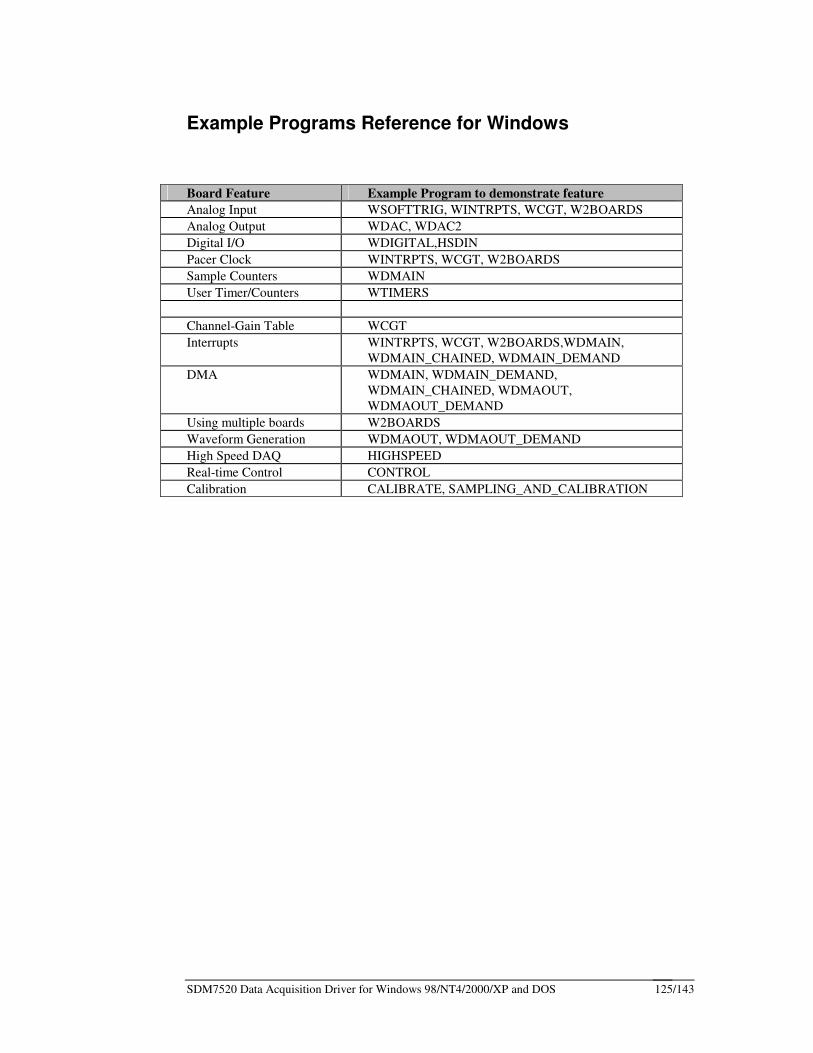
SDM7520 Data Acquisition Driver for Windows 98/NT4/2000/XP and DOS 125/143
Example Programs Reference for Windows Board Feature Example Program to demonstrate feature Analog Input WSOFTTRIG, WINTRPTS, WCGT, W2BOARDS Analog Output WDAC, WDAC2 Digital I/O WDIGITAL,HSDIN Pacer Clock WINTRPTS, WCGT, W2BOARDS Sample Counters WDMAIN User Timer/Counters WTIMERS Channel-Gain Table WCGT Interrupts WINTRPTS, WCGT, W2BOARDS,WDMAIN,
WDMAIN_CHAINED, WDMAIN_DEMAND DMA WDMAIN, WDMAIN_DEMAND,
WDMAIN_CHAINED, WDMAOUT, WDMAOUT_DEMAND
Using multiple boards W2BOARDS Waveform Generation WDMAOUT, WDMAOUT_DEMAND High Speed DAQ HIGHSPEED Real-time Control CONTROL Calibration CALIBRATE, SAMPLING_AND_CALIBRATION

SDM7520 Data Acquisition Driver for Windows 98/NT4/2000/XP and DOS 127/143
2 Channel DMA (wiodma) GUI (MFC) Example
Example on how to use two DMA channels simultaneously. The program shows how to program the SDM7540 to output samples through a DMA channel and read analog data simultaneously on the other DMA channel. This example uses the first installed SDM7540. The pacer clock is programmed to perform sampling at the rate of 48kHz. DMA channel 0 is programmed in demand mode, requesting DMA transfer when the A/D FIFO is half full. The DMA transfer is continued until the programmed number of samples are transferred. Then an interrupt service routine is activated on DMA-done. In the interrupt routine an IRQ counter is incremented and the sampling is stopped. The samples are graphically displayed on the screen, and then the sampling is restarted. The second DMA channel is programmed to transfer data from PCI memory to the DAC FIFO. Analog output 1 is programmed for bipolar 5 V. A sine-wave is generated and the calculated samples are placed in the DMA buffer. In this program the D/A 1 update counter is programmed to initiate a DMA cycle in the demand mode data transfer. If the analog input 1 is connected to the analog output 1, the generated sine-wave is graphed on the screen.
About Counter (abtctrio) Console Example
This example demonstrates using the about counter to delay pacer clock stop. This is useful for stopping sampling some number of samples after an interesting event. For the example, Data Marker 0 (cn6 pin 5) must be connected to Syncbus 1 and cn6 pin 7. First, 5 samples are taken. At that time the DIO pin is brought high, which brings the marker bit high and also brings syncbus 1 high. Syncbus 1 going high is the signal that starts the about counter counting down. When the counter reaches zero the pacer clock is stopped.
A/D Sample Counter (adsampct) Console Example
This example demonstrates using the A/D sample counter to count samples taken. First, an ISR is set up to be called on A/D sample countdown. Then the sample counter is loaded and software conversions are started. The sample counter decrements with every conversion taken until it reaches zero (in this case after 10 samples). Then an interrupt is generated and the sample counter is loaded again (done by hardware automatically) and as more samples are taken it counts down again. This repeats 3 times and the program ends.
SDM7520 Data Acquisition Driver for Windows 98/NT4/2000/XP and DOS 128/143
Automatic Multiburst (wamltbrst) GUI (MFC) Example Sample program that demonstrates how to use the pacer clock, burst clock, about counter and channel gain table to scan groups of channels, multiple times. This example uses the first installed SDM7540. This program will show how to use the about counter, burst clock and the pacer clock features to do MULTI-BURST sampling. The board will be set up to sample a set of channels, every time the board receives a trigger from the on board 8254. While the measurement is running the acquired data on the A/D channels is displayed on the screen.
Burst Clock (wburstn) GUI (MFC) Example Sample program that demonstrates how to perform an analog to digital conversion on multiple channels using the channel gain table. Burst mode means that all the channels in the table are sampled once for each trigger. The time between channels is set by the burst clock. If the burst clock is set to the highest rate, this mode simulates simultaneous sampling. This example uses the first installed SDM7540. Sample program that uses the Burst Clock, Pacer clock and the channel gain table to acquire data on several channels. The burst clock will start the conversions and the burst clock will be triggered by the pacer clock. While the measurement is running the acquired data on the A/D channels is displayed on the screen.
Calibrate (calibrate) GUI (MFC) Example Sample program that demonstrates calibrating the board programmatically. The GUI also allows the user to specify if the D/A’s will be calibrated and what to set the D/A’s output to after calibration.
CGT Example (wcgt) GUI (MFC) Example
Example on using the Channel-Gain Table. This example samples two Analog Input channels and saves data to disk. On the screen, it monitors number of samples saved. This example uses the first installed SDM7540. The A/D converter is set up for Pacer Clock controlled conversions. The Internal Pacer Clock is programmed for 1kHz, software start/stop. Cannel-Gain Table filled with two entries to sample AIN1 and AIN2 as single-ended channels, in 5Volts bipolar range. Interrupts are enabled on About Counter countdown. When the Start button is pressed, an interrupt handler is installed, the Pacer Clock is started, and a Windows timer is programmed to provide the main polling loop. The interrupt handler reads 512 samples from the A/D FIFO and saves them on disk.
SDM7520 Data Acquisition Driver for Windows 98/NT4/2000/XP and DOS 129/143
In the polling loop the interrupt counter is monitored.
Chained DMA (wdmain_chained) GUI (MFC) Example
Example on normal chained mode DMA input. The program shows how to program the SDM7540 to perform chained mode DMA transfers. This example uses the first installed SDM7540. The pacer clock is programmed to perform sampling at the rate of 10 kHz. The sample counter is programmed to generate interrupts when the A/D FIFO is half full. In the IRQ routine the DMA is started and the data is read from the FIFO. The DMA is programmed in chained mode and the DMA transfer can be initiated with software start. In this example program four chaining mode descriptor blocks are defined. In every descriptor block the DMA controller is programmed to read samples from the A/D FIFO and transfer the samples to different PCI memory locations. All of the descriptor blocks are setup to transfer 128 samples, thus on interrupt the A/D FIFO is emptied. The samples are graphically displayed on the screen. The four DMA transfers are visible on the screen with the gaps between them filled with the default character used by the InstallDMA7540 routine.
D/A Conversion (wdac) GUI (MFC) Example
Example on doing simple Digital/Analog conversions. The output voltage on D/A1 can be changed by an on-screen slider. If D/A1 is hooked back to Analog Input channel 1 (AIN1), this example program monitors the voltage on D/A1. This example uses the first installed SDM7540. D/A1 is programmed for 5V bipolar range, software update mode. AIN1 is sampled via the Channel-Gain Latch with software started conversions. A Windows timer is programmed to provide the main program loop. During every iteration, an A/D conversion is initiated to sample AIN1 and display the voltage on the screen. D/A1 is updated from software when the slider is moved.
D/A Update Counter (daupctr) Console Example
Example using the D/A Update counter. The D/A is set up for software DAC updates. The update counter is loaded with the value 5 and the Update Counter interrupt is enabled and an ISR function is created to handle the interrupt.
SDM7520 Data Acquisition Driver for Windows 98/NT4/2000/XP and DOS 130/143
Next, software D/A updates are performed. When 5 updates are completed the Interrupt Routine is called which causes output to the screen saying that the five updates interrupt has occurred. The program continues until a key is pressed.
Delay Counter (delayctr) Console Example
Example using the Pacer clock delay counter. The Pacer clock is set up to start sampling on delayed syncbus. Syncbus 1 must be connected to DIO 1 pin 7 (CN6 pin #2). Then the Pacer clock is armed by calling StartPacer. Then DIO 1 Pin 7 is brought high which sends a syncbus pulse to syncbus 1 and starts the delay counter counting down. When the counter reaches zero the pacer clock is started.
Demand Mode DMA Input (wdmain_demand) GUI(MFC) Example
Example on demand mode DMA input. The program shows how to program the SDM7540 to read samples through the DMA channel in demand mode. This example uses the first installed SDM7540. The pacer clock is programmed to perform sampling at the rate of 1.25 MHz. The DMA is programmed in demand mode, requesting DMA transfer when the A/D FIFO is half full. This program shows how to operate on the maximum (1.25 MHz) sample rate. The board can operate on the maximum sampling rate and transfers the data to the allocated PCI memory (DMA buffer). The DMA transfer is continued until the programmed number of samples is transferred. There is an interrupt service routine activated on DMA-done. In the interrupt routine an IRQ counter is incremented and the sampling is stopped. The samples are graphically displayed on the screen, and then the sampling is restarted.
Demand Mode DMA Output (wdmaout_demand) GUI (MFC) Example
Example on demand mode DMA output. The program shows how to program the SDM7540 to output samples through the DMA channel initiated by a hardware event. This example uses the first installed SDM7540. The analog output 1 is programmed on bipolar 5 V. A sine wave is generated and the calculated samples are placed in the DMA buffer. In this program the D/A 1 FIFO half empty bit is programmed to initiate a DMA cycle in the demand mode data transfer. The DMA done bit is programmed to generate an interrupt to restart the DMA transfer and load new samples in the DAC FIFO. A wave counter is displayed on the screen during the running of the program.
SDM7520 Data Acquisition Driver for Windows 98/NT4/2000/XP and DOS 131/143
Digital IO (wdigital) GUI (MFC) Example
Example on reading/writing the Digital I/O ports. Digital I/O Port 1 can be written by entering a value and pressing the Start button. Port 0 is polled on a timer. Hook back Port 1 to Port 0 to read back the value written to Port 1 on Port 0 This example uses the first installed SDM7540. Digital I/O Port 0 is programmed for input, Port 1 is programmed for output. A Windows timer is programmed to provide the main program loop. In every iteration Port 0 is read and displayed on screen. Pressing the Start button initiates writing to Port 1.
DMA Output (wdmaout) GUI (MFC) Example
Example on normal mode DMA output. The program shows how to program the SDM7540 to output samples through the DMA channel. This example uses the first installed SDM7540. The analog output 1 is programmed on bipolar 5 V. A sine wave is generated and the calculated samples are placed in the DMA buffer. The D/A update counter is programmed to generate an interrupt on countdown and restart the DMA transfer to load new samples to the DAC FIFO. A wave counter is displayed on the screen during the running of the program.
Driver Demo (drvr_demo) GUI (MFC) Example
This is a complex example on using the various driver functions to build a multifunctional program. This example uses the first installed SDM7540.
Graphic DMA (wdmain) GUI (MFC) Example
Example on normal mode DMA input. The program shows how to program the SDM7540 to read samples through the DMA channel. This example uses the first installed SDM7540. The pacer clock is programmed to perform sampling at 10 kHz. The sample counter is programmed to generate an interrupt when the A/D FIFO is half-full. In the interrupt routine an IRQ counter is incremented and the DMA is restarted.
SDM7520 Data Acquisition Driver for Windows 98/NT4/2000/XP and DOS 132/143
The samples are graphically displayed on the screen.
High Speed Data Acquisition (highspeed) GUI (MFC) Example
This program demonstrates how to perform high-speed data acquisition for a long time. In this program the speed is 64 kByte/s. The program allocates a large memory buffer (2 Mbytes) for the temporary storage of the samples. This buffer could be as large as your system memory allows for you. The CGT will be programmed to sample 8 channels. The conversions are initiated by the burst clock. The burst clock starts on pacer clock. The samples will be transferred from the A/D FIFO to the DMA buffer with demand mode DMA. On DMA done interrupt in the ISR routine the samples will be copied to the memory buffer. If the memory buffer is full, the data acquisition will be stopped and the content of the buffer is transferred to the hard disk. The speed of the DAQ rate in this program depends on your computer's speed. The program is using CPU resources to transfer the samples from the DMA buffer to the memory buffer in the DMA done interrupt routine. This example uses the first installed SDM7540.
High Speed Digital Input (hsdin) GUI (MFC) Example
This program demonstrates the use of High Speed Digital Input. The UTC0 is programmed to sample the HSDIN at the defined RATE. UTC1 is programmed to count these samples and initiate a demand mode DMA cycle when the programmed number of samples is received. DMA completion generates an interrupt to inform the main program that the samples are ready to copy from the DMA buffer to the user buffer. The digital output of the board is used to generate input data for HSDIN (0xA5). The output of digital I/O is internally connected to HSDIN, thus the program reads back this data without any wiring. The sample buffer is displayed on the screen.
Interrupts (wintrpts) GUI (MFC) Example Example program to demonstrate interrupt handling routines. The board is programmed to sample analog input 1 with the pacer clock. On A/D conversion, the board generates an interrupt. The samples are read and displayed on the screen after an interrupt occurs. The example uses the first installed SDM7540.
Load Defaults (Load_Defaults) GUI (MFC) Example Example program to demonstrate loading failsafe default calibration settings. Each SDM7540 is programmed with fail safe defaults at the factory. This utility demonstrates instructing the board to use the defaults instead of the last calibrated values. Calibrating the
SDM7520 Data Acquisition Driver for Windows 98/NT4/2000/XP and DOS 133/143
board takes precedence over the failsafe defaults. If you calibrate the board after loading the defaults, the last calibrated values are used until you load defaults again.
Multi Channel with Pacer (wamltscan) GUI (MFC) Example Sample program that demonstrates how to use the pacer clock, about counter and channel gain table to scan groups of channels, multiple times. This example uses the first installed SDM7540. This program will show how to use the about counter and the pacer clock features to do MULTI-SCAN sampling. The board will be set up to sample a set of channels, every time the board receives a trigger from the on board 8254. While the measurement is running the acquired data on the A/D channels is displayed on the screen.
One Cycle Output Generation (wdac2) GUI (MFC) Example
Example on how to generate a singe cycle on the analog output. The program demonstrates the using of the DAC clock start/stop trigger selection function and software DAC clock start. This example uses the first installed SDM7540. D/A1 is programmed for 5V bipolar range, DAC Clock update mode. When the user presses a button, a single sine wave cycle is generated on AOUT1.
Random Channel Sampling (wrandom) GUI (MFC) Example
Example on doing multiple-channel Analog/Digital conversions using the Channel Gain Table. This example uses the first installed SDM7540. The Channel-Gain Table is programmed to sample AIN1-AIN16 channels in 5Volts bipolar, single-ended mode. A/D converter is programmed for pacer clock triggered conversions. When pressing the Start button, an A/D conversion is initiated and the samples are displayed on the screen as Voltage. There is a slider in the window to change the pacer clock frequency. AOUT1 and AOUT2 are programmed to generate an output voltage of 90% of full scale input values. The gain is selectable in the program between 1-32. The AOUT values are changed according to the gain, because in case of higher gain the input range changes.
Real Time Control (control) GUI (MFC) Example
This program demonstrates how to perform real-time control. The program is a simple "stereo volume control" application. The channel gain table is programmed to sample two analog channel with burst clock. The rate of burst clock is
SDM7520 Data Acquisition Driver for Windows 98/NT4/2000/XP and DOS 134/143
programmed to 1 MHz and the CGT is started with pacer clock. The pacer clock rate is variable, using a scrollbar control. Two analog outputs are defined. The sampled analog inputs are transferred to the DMA buffer with demand mode DMA started on A/D FIFO half full. On DMA done interrupt an ISR is called. In this example we simple multiply the analog values with a variable gain and the new values are transferred to the D/A FIFO. As the D/A update source is the CGT (D/A is updated when a new CGT row is processed), the analog input and the analog output will be synchronized and they are jitter-free. However, there is a phase shift between the real analog input and output due the programmatic data transfer from the DMA buffer to the D/A FIFO. This delay depends on the pacer clock rate. This example uses the first installed SDM7540.
Sampling and Calibration (Sampling_and_Calibration) Console Example
This program demonstrates the setup required when calibration is called between taking samples. No assumptions can be made as to the state of board registers after calibration so re-setup is required.
Software Trigger (wsofttrig) GUI (MFC) Example
Example on doing simple Analog/Digital conversions. This example program performs an A/D conversion when a button is pressed. This example uses the first installed SDM7540. Channel-Gain Latch is programmed for AIN1, 5Volts bipolar, single-ended. A/D converter is programmed for software triggered conversions. When the start button is pressed, an A/D conversion is initiated and the sample is displayed on screen as Voltage.
Temperature (temperature) GUI (MFC) Example
Demonstrates reading the temperature of the board.
Timers (wtimers) GUI (MFC) Example
Example on programming the User Timer/Counters. This example counts seconds in real-time. This example uses the first installed SDM7540. User Timer/Counter 0 and 1 are cascaded. Counter 0 is programmed for 200 Hertz. When pressing the Start button a Windows timer is programmed for 200 msec to provide the main program loop. In every iteration User Timer/Counter 1 count is read back and converted to seconds.
SDM7520 Data Acquisition Driver for Windows 98/NT4/2000/XP and DOS 135/143
Update Autocalibration Algorithm (update) GUI (MFC) Example
This program is used to update the autocalibration algorithm in internal DSP flash memory. When the board is shipped it already has the latest algorithm in DSP flash memory. From time to time RTD might make alterations to the algorithm or add new functionality. With this utility you can keep your board up to date.
Using Two Boards (w2boards) GUI (MFC) Example
Example on using two SDM7540 boards in an application. This example samples AIN1 on two SDM7540s. Sampling on the two boards can be started/stopped independently. This example uses the first two installed SDM7540 boards. Both boards are configured in the same way. A/D converters are set up for Pacer Clock controlled conversions. The Internal Pacer Clocks are programmed for 5/10Hz, software start/stop. Cannel-Gain Latches are set up for sampling AIN1, single-ended channels, in 5Volts bipolar range. Interrupts are enabled on A/D FIFO Write. When a Start button is pressed, an interrupt handler is installed for the corresponding board, its Pacer Clock is started, and a Windows timer is programmed to provide the polling loop. The interrupt handlers read 1 sample from the A/D FIFO, which is displayed in the polling loop.
Version (version) GUI (MFC) Example This utility reports the version numbers of the boot loader and autocalibration algorithms on the DSP.
Analog_DIO_Test (Analog_DIO_Test) Console Example This example demonstrates the use of the two DIO pins on the analog connector (CN9). Pins 1 and 2 must be connected with a wire. Analog_DIO pin 1 is set to be an output and pin 2 is set to be an input. We enable interrupts on the positive edge of pin 2. Then we bring pin 1 high ten times and make sure we received 10 interrupts from pin 2.
SDM7520 Data Acquisition Driver for Windows 98/NT4/2000/XP and DOS 136/143
Example Programs Reference for DOS
About Counter (abtctrio)
This example demonstrates using the about counter to delay pacer clock stop. This is useful for stopping sampling some number of samples after an interesting event. For the example, Data Marker 0 (cn6 pin 5) must be connected to Syncbus 1 and cn6 pin 7. First, 5 samples are taken. At that time the DIO pin is brought high, which brings the marker bit high and also brings syncbus 1 high. Syncbus 1 going high is the signal that starts the about counter counting down. When the counter reaches zero the pacer clock is stopped.
A/D Sample Counter (adsampct)
This example demonstrates using the A/D sample counter to count samples taken. First, an ISR is set up to be called on A/D sample countdown. Then the sample counter is loaded and software conversions are started. The sample counter decrements with every conversion taken until it reaches zero (in this case after 10 samples). Then an interrupt is generated and the sample counter is loaded again (done by hardware automatically) and as more samples are taken it counts down again. This repeats 3 times and the program ends.
Automatic Multiburst (amltbrst) Sample program that demonstrates how to use the pacer clock, burst clock, about counter and channel gain table to scan groups of channels, multiple times. This example uses the first installed SDM7540. This program will show how to use the about counter, burst clock and the pacer clock features to do MULTI-BURST sampling. The board will be set up to sample a set of channels, every time the board receives a trigger from the on board 8254. While the measurement is running the acquired data on the A/D channels is displayed on the screen.
Multi Channel with Pacer (amltscan) Sample program that demonstrates how to use the pacer clock, about counter and channel gain table to scan groups of channels, multiple times. This example uses the first installed SDM7540. This program will show how to use the about counter and the pacer clock features to do MULTI-SCAN sampling. The board will be set up to sample a set of channels, every time the board receives a trigger from the on board 8254. While the measurement is running the acquired data on the A/D channels is displayed on the screen.
SDM7520 Data Acquisition Driver for Windows 98/NT4/2000/XP and DOS 137/143
Analog_DIO_Test (anlogDIO) This example demonstrates the use of the two DIO pins on the analog connector (CN9). Pins 1 and 2 must be connected with a wire. Analog_DIO pin 1 is set to be an output and pin 2 is set to be an input. We enable interrupts on the positive edge of pin 2. Then we bring pin 1 high ten times and make sure we received 10 interrupts from pin 2.
Burst Clock (burst_n) Sample program that demonstrates how to perform an analog to digital conversion on multiple channels using the channel gain table. Burst mode means that all the channels in the table are sampled once for each trigger. The time between channels is set by the burst clock. If the burst clock is set to the highest rate, this mode simulates simultaneous sampling. This example uses the first installed SDM7540. Sample program that uses the Burst Clock, Pacer clock and the channel gain table to acquire data on several channels. The burst clock will start the conversions and the burst clock will be triggered by the pacer clock. While the measurement is running the acquired data on the A/D channels is displayed on the screen.
Calibrate (calibrat) Sample program that demonstrates calibrating the board programmatically. Parameters allow the user to specify if the D/A’s will be calibrated and what to set the D/A’s output to after calibration.
D/A Conversion (dac)
Example on doing simple Digital/Analog conversions. D/A1 should be wired to AIN1 for this example. The output voltage on D/A1 is cycled and the difference between the set D/A voltage and the sampled AIN voltage is displayed on screen. This example uses the first installed SDM7540. D/A1 is programmed for 5V bipolar range, software update mode. AIN1 is sampled via the Channel-Gain Latch with software started conversions.
D/A Update Counter (daupctr)
Example using the D/A Update counter. The D/A is set up for software DAC updates. The update counter is loaded with the value 5 and the Update Counter interrupt is enabled and an ISR function is created to handle the interrupt.
SDM7520 Data Acquisition Driver for Windows 98/NT4/2000/XP and DOS 138/143
Next, software D/A updates are performed. When 5 updates are completed the Interrupt Routine is called which causes output to the screen saying that the five updates interrupt has occurred. The program continues until a key is pressed.
Delay Counter (delayctr)
Example using the Pacer clock delay counter. The Pacer clock is set up to start sampling on delayed syncbus. Syncbus 1 must be connected to DIO 1 pin 7 (CN6 pin #2). Then the Pacer clock is armed by calling StartPacer. Then DIO 1 Pin 7 is brought high which sends a syncbus pulse to syncbus 1 and starts the delay counter counting down. When the counter reaches zero the pacer clock is started.
Digital IO (digital)
Example on reading/writing the Digital I/O ports. Digital I/O Port 1 can be written by entering a value. Hook back Port 1 to Port 0 to read back the value written to Port 1 on Port 0 This example uses the first installed SDM7540. Digital I/O Port 0 is programmed for input, Port 1 is programmed for output.
DMA Input (dmain)
Example on normal mode DMA input. The program shows how to program the SDM7540 to read samples through the DMA channel. This example uses the first installed SDM7540. The pacer clock is programmed to perform sampling at 10 kHz. The sample counter is programmed to generate an interrupt when the A/D FIFO is half-full. In the interrupt routine an IRQ counter is incremented and the DMA is restarted.
DMA Demand Mode Input (dmaind)
Example on demand mode DMA input. The program shows how to program the SDM7540 to read samples through the DMA channel. This example uses the first installed SDM7540. The pacer clock is programmed to perform sampling at 10 kHz. A DMA is set up to transfer data on A/D FIFO half full. In the interrupt routine a flag is set that indicates there are new samples waiting and the pacer clock is stopped. In the main program loop the new samples flag is checked, if it is TRUE then a sample is displayed on screen, the Pacer clock is restarted and the DMA is started again.
SDM7520 Data Acquisition Driver for Windows 98/NT4/2000/XP and DOS 139/143
DMA Output (dmaout)
Example on normal mode DMA output. The program shows how to program the SDM7540 to output samples through the DMA channel. This example uses the first installed SDM7540. The analog output 1 is programmed on bipolar 5 V. A sine wave is generated and the calculated samples are placed in the DMA buffer. The D/A update counter is programmed to generate an interrupt on countdown and restart the DMA transfer to load new samples to the DAC FIFO. A wave counter is displayed on the screen during the running of the program.
Demand Mode DMA Output (dmaoutd)
Example on demand mode DMA output. The program shows how to program the SDM7540 to output samples through the DMA channel initiated by a hardware event. This example uses the first installed SDM7540. The analog output 1 is programmed on bipolar 5 V. A sine wave is generated and the calculated samples are placed in the DMA buffer. In this program the D/A 1 FIFO half empty bit is programmed to initiate a DMA cycle in the demand mode data transfer. The DMA done bit is programmed to generate an interrupt to restart the DMA transfer and load new samples in the DAC FIFO. A wave counter is displayed on the screen during the running of the program.
A/D FIFO (fifo) Sample program that demonstrates how to acquire data at a specified frequency until the FIFO is full. After the sampling period is over, the data is displayed on the screen.
Interrupts (intrpts) Example program to demonstrate interrupt handling routines. A user timer/counter is set up to generate interrupts. When an interrupt occurs, a software sample is taken. That sample is displayed on screen.
Load Defaults (loaddef) Example program to demonstrate loading failsafe default calibration settings.
SDM7520 Data Acquisition Driver for Windows 98/NT4/2000/XP and DOS 140/143
Each SDM7540 is programmed with fail safe defaults at the factory. This utility demonstrates instructing the board to use the defaults instead of the last calibrated values. Calibrating the board takes precedence over the failsafe defaults. If you calibrate the board after loading the defaults, the last calibrated values are used until you load defaults again.
Multi Channel Sampling (multi_ch)
Example on doing multiple-channel Analog/Digital conversions using the Channel Gain Table. This example uses the first installed SDM7540. The Channel-Gain Table is programmed to sample AIN1-AIN16 channels in 5Volts bipolar, single-ended mode. A/D converter is programmed for pacer clock triggered conversions. When pressing the Start button, an A/D conversion is initiated and the samples are displayed on the screen as Voltage.
Sampling and Calibration (sampcal)
This program demonstrates the setup required when calibration is called between taking samples. No assumptions can be made as to the state of board registers after calibration so re-setup is required.
Multi Channel Scanning (scan_n) Sample program that demonstrates how to perform an analog to digital conversion on multiple channels using the channel gain table. Scan mode means that the time between two samples is equally divided among the channels. While the measurement is running the acquired data on the A/D channels is displayed on the screen, one line with every sample.
Software Trigger (softtrig)
Example on doing simple Analog/Digital conversions. This example program performs software A/D conversions. This example uses the first installed SDM7540. Channel-Gain Latch is programmed for AIN1, 5Volts bipolar, single-ended. A/D converter is programmed for software triggered conversions. In a loop, an A/D conversion is initiated and the sample is displayed on screen as Voltage.
Timers (timers)
Example on programming the User Timer/Counters. This example counts seconds in real-time. This example uses the first installed SDM7540.
SDM7520 Data Acquisition Driver for Windows 98/NT4/2000/XP and DOS 141/143
User Timer/Counter 0 and 1 are cascaded. Counter 0 is programmed for 200 Hertz. In every iteration User Timer/Counter 1 count is read back and converted to seconds.
Temperature (tmprture)
Demonstrates reading the temperature of the board.
Update Autocalibration Algorithm (update)
This program is used to update the autocalibration algorithm in internal DSP flash memory. When the board is shipped it already has the latest algorithm in DSP flash memory. From time to time RTD might make alterations to the algorithm or add new functionality. With this utility you can keep your board up to date.
Version (version) GUI (MFC) Example This utility reports the version numbers of the boot loader and autocalibration algorithms on the DSP.
SDM7520 Data Acquisition Driver for Windows 98/NT4/2000/XP and DOS 142/143
Limited Warranty RTD Embedded Technologies, Inc. warrants the hardware and software products it manufactures and produces to be free from defects in materials and workmanship for one year following the date of shipment from RTD Embedded Technologies, INC. This warranty is limited to the original purchaser of product and is not transferable.
During the one year warranty period, RTD Embedded Technologies will repair or replace, at its option, any defective products or parts at no additional charge, provided that the product is returned, shipping prepaid, to RTD Embedded Technologies. All replaced parts and products become the property of RTD Embedded Technologies. Before returning any product for repair, customers are required to contact the factory for an RMA number.
THIS LIMITED WARRANTY DOES NOT EXTEND TO ANY PRODUCTS WHICH HAVE BEEN DAMAGED AS A RESULT OF ACCIDENT, MISUSE, ABUSE (such as: use of incorrect input voltages, improper or insufficient ventilation, failure to follow the operating instructions that are provided by RTD Embedded Technologies, "acts of God" or other contingencies beyond the control of RTD Embedded Technologies), OR AS A RESULT OF SERVICE OR MODIFICATION BY ANYONE OTHER THAN RTD Embedded Technologies. EXCEPT AS EXPRESSLY SET FORTH ABOVE, NO OTHER WARRANTIES ARE EXPRESSED OR IMPLIED, INCLUDING, BUT NOT LIMITED TO, ANY IMPLIED WARRANTIES OF MERCHANTABILITY AND FIT-NESS FOR A PARTICULAR PURPOSE, AND RTD Embedded Technologies EXPRESSLY DISCLAIMS ALL WARRANTIES NOT STATED HEREIN. ALL IMPLIED WARRANTIES, INCLUDING IMPLIED WARRANTIES FOR MECHANTABILITY AND FITNESS FOR A PARTICULAR PURPOSE, ARE LIMITED TO THE DURATION OF THIS WARRANTY. IN THE EVENT THE PRODUCT IS NOT FREE FROM DEFECTS AS WARRANTED ABOVE, THE PURCHASER'S SOLE REMEDY SHALL BE REPAIR OR REPLACEMENT AS PROVIDED ABOVE. UNDER NO CIRCUMSTANCES WILL RTD Embedded Technologies BE LIABLE TO THE PURCHASER OR ANY USER FOR ANY DAMAGES, INCLUDING ANY INCIDENTAL OR CONSEQUENTIAL DAMAGES, EXPENSES, LOST PROFITS, LOST SAVINGS, OR OTHER DAMAGES ARISING OUT OF THE USE OR INABILITY TO USE THE PRODUCT.
SOME STATES DO NOT ALLOW THE EXCLUSION OR LIMITATION OF INCIDENTAL OR CONSEQUENTIAL DAMAGES FOR CONSUMER PRODUCTS, AND SOME STATES DO NOT ALLOW LIMITATIONS ON HOW LONG AN IMPLIED WARRANTY LASTS, SO THE ABOVE LIMITATIONS OR EXCLUSIONS MAY NOT APPLY TO YOU.
THIS WARRANTY GIVES YOU SPECIFIC LEGAL RIGHTS, AND YOU MAY ALSO HAVE OTHER RIGHTS WHICH VARY FROM STATE TO STATE.
SDM7520 Data Acquisition Driver for Windows 98/NT4/2000/XP and DOS 143/143
RTD Embedded Technologies, Inc.
103 Innovation Blvd.
State College PA 16803-0906
USA
Our website: www.rtd.com