Embed Size (px)
Citation preview

T118B Advanced Information-Confidential P/N-T118B-Rev01 Copyright by Terawins, Inc.
1
Advanced Information Version 1.0
Nov 12, 2006
T118B Video Display Controller

T118B Advanced Information-Confidential P/N-T118B-Rev01 Copyright by Terawins, Inc.
2
Table of Contents
1 INTRODUCTION.......................................................................................................................................................... 3 1.1 FEATURES ................................................................................................................................................................. 3 1.2 GENERAL DESCRIPTION ............................................................................................................................................ 4 1.3 APPLICATIONS........................................................................................................................................................... 4 1.4 SYSTEM ARCHITECTURE ........................................................................................................................................... 5 1.5 SYSTEM CONFIGURATIONS........................................................................................................................................ 6 1.6 PINOUT DIAGRAM ..................................................................................................................................................... 7 1.7 PIN DESCRIPTION ...................................................................................................................................................... 8
2 THEORY OF OPERATIONS..................................................................................................................................... 10 2.1 I²C COMMAND PROTOCOL ...................................................................................................................................... 10 2.2 ANALOG FRONT END .............................................................................................................................................. 12 2.3 Y/C SEPARATION AND CHROMA DECODER............................................................................................................. 12 2.4 DIGITAL COLOR TRANSIENT IMPROVEMENT (DCTI) .............................................................................................. 14 2.5 DIGITAL LUMINANCE TRANSIENT IMPROVEMENT (DLTI) ...................................................................................... 15 2.6 FIR SCALER ............................................................................................................................................................ 15 2.7 BLACK-LEVEL EXTENSION (BLE)........................................................................................................................... 16 2.8 COLOR SPACE CONVERTER ..................................................................................................................................... 16 2.9 GAMMA CORRECTION ............................................................................................................................................. 17 2.10 OSD........................................................................................................................................................................ 18 2.11 TCON..................................................................................................................................................................... 30
3 REGISTER DESCRIPTION....................................................................................................................................... 33 3.1 ADC REGISTER SET ................................................................................................................................................ 33 3.2 PICTURE ENHANCEMENT REGISTER SET ................................................................................................................. 44 3.3 SCALING REGISTER SET .......................................................................................................................................... 46 3.4 COLOR SPACE CONVERTER REGISTER SET.............................................................................................................. 52 3.5 OSD REGISTER SET ................................................................................................................................................ 55 3.6 LCD OUTPUT CONTROL REGISTER SET .................................................................................................................. 56 3.7 TCON REGISTER SET.............................................................................................................................................. 69 3.8 Y/C SEPARATION AND CHROMA DECODER REGISTER SET...................................................................................... 74
4 ELECTRICAL CHARACTERISTICS...................................................................................................................... 83 4.1 DIGITAL I/O PAD OPERATION CONDITION .............................................................................................................. 83 4.2 AC CHARACTERISTICS ............................................................................................................................................ 84 4.3 ANALOG PROCESSING AND A/D CONVERTERS........................................................................................................ 84 4.4 ABSOLUTE MAXIMUM RATING ............................................................................................................................... 84
5 PACKAGE DIMENSIONS ......................................................................................................................................... 85
6 ORDERING INFORMATION ................................................................................................................................... 85
7 REVISIONS NOTE...................................................................................................................................................... 86
8 GENERAL DISCLAIMER ......................................................................................................................................... 86
9 CONTACT INFORMATION ..................................................................................................................................... 86
T118B Advanced Information-Confidential P/N-T118B-Rev01 Copyright by Terawins, Inc.
3
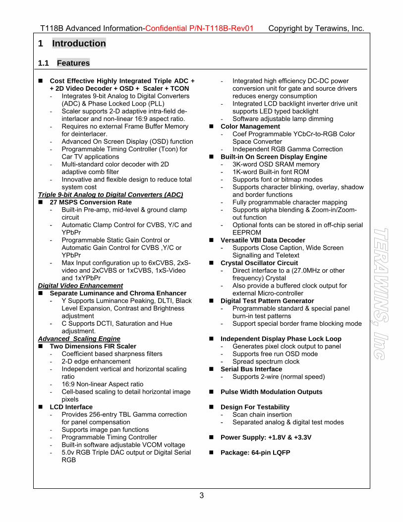
1 Introduction
1.1 Features
Cost Effective Highly Integrated Triple ADC + + 2D Video Decoder + OSD + Scaler + TCON - Integrates 9-bit Analog to Digital Converters
(ADC) & Phase Locked Loop (PLL) - Scaler supports 2-D adaptive intra-field de-
interlacer and non-linear 16:9 aspect ratio. - Requires no external Frame Buffer Memory
for deinterlacer. - Advanced On Screen Display (OSD) function - Programmable Timing Controller (Tcon) for
Car TV applications - Multi-standard color decoder with 2D
adaptive comb filter - Innovative and flexible design to reduce total
system cost Triple 9-bit Analog to Digital Converters (ADC)
27 MSPS Conversion Rate - Built-in Pre-amp, mid-level & ground clamp
circuit - Automatic Clamp Control for CVBS, Y/C and
YPbPr - Programmable Static Gain Control or
Automatic Gain Control for CVBS ,Y/C or YPbPr
- Max Input configuration up to 6xCVBS, 2xS-video and 2xCVBS or 1xCVBS, 1xS-Video and 1xYPbPr
Digital Video Enhancement Separate Luminance and Chroma Enhancer
- Y Supports Luminance Peaking, DLTI, Black Level Expansion, Contrast and Brightness adjustment
- C Supports DCTI, Saturation and Hue adjustment.
Advanced Scaling Engine Two Dimensions FIR Scaler
- Coefficient based sharpness filters - 2-D edge enhancement - Independent vertical and horizontal scaling
ratio - 16:9 Non-linear Aspect ratio - Cell-based scaling to detail horizontal image
pixels LCD Interface
- Provides 256-entry TBL Gamma correction for panel compensation
- Supports image pan functions - Programmable Timing Controller - Built-in software adjustable VCOM voltage - 5.0v RGB Triple DAC output or Digital Serial
RGB
- Integrated high efficiency DC-DC power conversion unit for gate and source drivers reduces energy consumption
- Integrated LCD backlight inverter drive unit supports LED typed backlight
- Software adjustable lamp dimming Color Management
- Coef Programmable YCbCr-to-RGB Color Space Converter
- Independent RGB Gamma Correction Built-in On Screen Display Engine
- 3K-word OSD SRAM memory - 1K-word Built-in font ROM - Supports font or bitmap modes - Supports character blinking, overlay, shadow
and border functions - Fully programmable character mapping - Supports alpha blending & Zoom-in/Zoom-
out function - Optional fonts can be stored in off-chip serial
EEPROM Versatile VBI Data Decoder
- Supports Close Caption, Wide Screen Signalling and Teletext
Crystal Oscillator Circuit - Direct interface to a (27.0MHz or other
frequency) Crystal - Also provide a buffered clock output for
external Micro-controller Digital Test Pattern Generator
- Programmable standard & special panel burn-in test patterns
- Support special border frame blocking mode
Independent Display Phase Lock Loop - Generates pixel clock output to panel - Supports free run OSD mode - Spread spectrum clock
Serial Bus Interface - Supports 2-wire (normal speed)
Pulse Width Modulation Outputs
Design For Testability - Scan chain insertion - Separated analog & digital test modes
Power Supply: +1.8V & +3.3V
Package: 64-pin LQFP

T118B Advanced Information-Confidential P/N-T118B-Rev01 Copyright by Terawins, Inc.
4
1.2 General Description The T118B is a highly integrated All-in-one Visual Processor that provides major cost saving solution for the portable applications. T118B has built-in high performance dual ADCs (support YCbCr), TCON, Triple DACs, Scaling Machine with sophisticated upscaling and downscaling algorithms.
The Innovative integrated “Frame-Buffer-Less” De-interlacer can significantly reduce system cost. The T118B also integrates On Screen Display engine with 3K-words of font RAM and built-in 1K-words of font ROM. The device can interface to an external micro-controller through 2-wire serial bus interface.
1.3 Applications
1. 1.8-inch to 10-inch portable DVD or in-car TV 2. Progressive CRT TV

T118B Advanced Information-Confidential P/N-T118B-Rev01 Copyright by Terawins, Inc.
5
1.4 System Architecture
Input Sample Rate
Converter
Y/C SeparationAnalog
Front End ControlADC
ADC
T118B Block Diagram
Peaking DLTI
DCTI
Contrast / Brightness
Saturation / Hue
Y
CbCr CbCr
Y
2D-Adaptive Comb Filter
Line Buffer
Line Buffer
Line Buffer
Line Buffer
U/V Demodulation
YCbCrPost-filtering
Format Detection
InputCapture
Scaler
Line Buffer
Line Buffer
Line Buffer
Line Buffer
OSD RAM
GammaBlack Level Expansion
OSD
CSCDither Timing
Gen
LCD Out Control
TCON
Pin MU
X
RSTB 2-Wire Slave
SDA, SCL
SCAN TEST LOGIC
SCAN_MODE
Display PLL
XCLK
I
X CLK
O
X CLK
2 MC
PT_GEN +DACDACDAC
ADC
DC-to-DC Converter
LED
Figure 1-1 System Architecture

T118B Advanced Information-Confidential P/N-T118B-Rev01 Copyright by Terawins, Inc.
6
© Copyright 2006 Terawins, Inc.
1.5 System Configurations
T118BVideo
DisplayController
TCON Signals
8051
MCU
CVBS
S-VIDEO
TV Tuner
Y
C
Component
Y
Pb
Pr TFT-LCD
DAC Blue Data
DAC Red Data
DAC Green Data
HV DC-DC, BL Dimming
Figure 1-2 System Configuration

T118B Advanced Information-Confidential P/N-T118B-Rev01 Copyright by Terawins, Inc.
7
1.6 Pinout Diagram
GCLK/sD4LP/OEH/sD3Q1H/sD2CPH3/sD1CPH2/sD0GNDVDD18CPH1DEN/STH2VSO/STH1VDD33GNDHSO/POL/VCOMUDRLPWM2
AY1
AY0
ACR
1AC
R0
ACB1
ACB0
GN
DV
DD
18R
STB
SD
A/IIC
A3S
CL
CP
UIN
TX
TALI
XTA
LOXC
LK2M
CP
WM
1
1 2 3 4 5 6 7 8 9 10 11 12 13 14 15 16
32313029282726252423222120191817
48 47 46 45 44 43 42 41 40 39 38 37 36 35 34 33
49505152535455565758596061626364
VEACSSVFB
CEXTVPWM
VEALVFBL
VPWMLCSSL
CEXTLVIsenLVIsen
NCVS33PWM
VD33ADC1/VD33ADC2VS33ADC1/VS33ADC2
VS
18P
LL
VD
33P
WM
VC
OM
DC
VC
OM
AM
PV
BFG
RS
ETIO
RIO
GIO
BV
S33
VD
5AG
ND
VD
D33
STV
2/sD
7S
TV1/
sD6
GO
E/sD
5
VD
33D
AC/
DA
C
V1.0
Figure 1-3 Pinout Diagram
© Copyright 2006 Terawins, Inc.

T118B Advanced Information-Confidential P/N-T118B-Rev01 Copyright by Terawins, Inc.
8
1.7 Pin Description
Table 1-1 Pin Description Symbol Pin # Type Description
Power Supplies VDD18 8,26 PWR +1.8V digital core power supply VDD33 22,36 PWR +3.3V digital output power supply, VD5A 38 PWR +5.0V analog power supply
VD33ADC1 VD33ADC2
63 PWR +3.3V analog power supply for ADC
VD33DAC VD33PWM
47 PWR +3.3V analog power supply for DAC
GND 7,21,27,37 GND Digital ground VS18PLL 48 GND Analog ground for PLL
VS33ADC1 VS33ADC2
64 GND Analog ground for ADC
VS33DAC 39 GND Analog ground for DAC VS33PWM 62 GND Analog ground for backlight inverter
Output Interface Signals RSET 43 AO DAC reference current adjustment VBFG 44 AO Voltage reference output IOR 42 AO Channel R current output IOG 41 AO Channel G current output IOB 40 AO Channel B current output
CPH1 25 DO Output data clock CPH2/sD0 28 DO Output data clock/the bit 0 of serial interfaced panel CPH3/sD1 29 DO Output data clock/the bit 1 of serial interfaced panel VSO/STH1 23 DO Vertical synchronization output signal. HSO/POL 20 DO Horizontal synchronization output signal. DEN/STH2 24 DO Horizontal data enable
Timing Controller Interface Signals UD 19 DO Vertical Up/Down control RL 18 DO Horizontal Right/Left control
Q1H/sD2 30 DO Source Driver Q1H/the bit 2 of serial interfaced panel LP/sD3 31 DO Latch pulse for source driver/the bit 3 of serial interfaced panel
GCLK/sD4 32 DO Gate driver clock/the bit 4 of serial interfaced panel GOE/sD5 33 DO Gate driver output enable/the bit 5 of serial interfaced panel STV1/sD6 34 DO Gate Driver start pulse/the bit 6 of serial interfaced panel STV2/sD7 35 DO Gate Driver start pulse/the bit 7 of serial interfaced panel
VCOMAMP 45 DO Analog VCOM amplitude VCOMDC 46 DO Analog VCOM DC offset
2-wire serial bus Interface Signals SCL 11 DI 2-wire serial bus clock. Power down does not affect SCL.
SDA/IICA3 10 I/O 2-wire serial bus data. Power down does not affect SDA.
Configuration interface Signals CPUINT 12 I/O Internal Interrupt. RSTB 9 DI Whole chip reset. (Internal Pull-up)

T118B Advanced Information-Confidential P/N-T118B-Rev01 Copyright by Terawins, Inc.
9
Symbol Pin # Type Description
ADC Interface AY1 1 AI Analog input 1 of input channel 2 AY0 2 AI Analog input 0 of input channel 2
ACR1 3 AI Analog input 1 of input channel 1 ACR0 4 AI Analog input 0 of input channel 1 ACB1 5 AI Analog input 1 of input channel 3 ACB0 6 AI Analog input 0 of input channel 3
PLL Reference Clock XTALI 13 DI Output PLL reference clock input XTALO 14 DO Output PLL reference clock output
XCLK2MC 15 DO Buffered XTALI for external microprocessor.
Power Management Interface Signals PWM1 16 DO Pulse Width Modulation for volume/backlight control. PWM2 17 DO Pulse Width Modulation for volume/backlight control. VEA 49 AO Error amplifier output CSS 50 AO Soft start pin VFB 51 AI Feedback of Lamp current
CEXT 52 AO Switching frequency of DC-DC converter VPWM 53 AO PWM output, connect to external N-channel power MOSFET VEAL 54 AO Error Amplifier output VFBL 55 AI Feedback of Lamp current
VPWML 56 AO PWM output, drive NMOSFET switch CSSL 57 AO Soft start pin
CEXTL 58 AO Switching frequency of Inverter VIsenL 59 AI Current sense VIsen 60 AI Current sense
NC 61 N/A

T118B Advanced Information-Confidential P/N-T118B-Rev01 Copyright by Terawins, Inc.
10
2 Theory of Operations
2.1 I²C Command Protocol
Before your tester writes I²C commands to T118B, slave address must be set at 50h. The timing
sequence can be shown as below. After 4 cycles, the tester can get started IIC commands. SDA(A3) can affect slave address. Set low for 40h. Set high for 50h.
XTALI
RSTB
SDADon`t care
2 Cycles 2 Cycles
SCLDon`t care
Figure 2-1 Power-up initialization
When tester issues commands to the T118B, the only way the user can program the T118B is
using the 2-wire serial bus protocol. This section describes the 2-wire serial bus protocol. Data transfers on the 2-wire serial bus are initiated with a START condition and are terminated with a STOP condition. Normal data on the SDA line must be stable during the high period of the SCL. The transition on the SDA is only allowed while SCL is low. The START condition is unique case and is defined by a high-to-low transition on the SDA while the SCL is high. The STOP condition is a unique case and is defined by a low-to-high transition on the SDA while the SCL is high. Each data packet on the 2-wire serial bus consists of 8 bits of data followed by an ACK bit. Data is transferred with MSB first. The transmitter releases the SDA line during the ACK bit and the receiver of data transfer must drive the SDA line low during the ACK bit to acknowledge receipt of the data. The frequency of SCL can be from 50 Khz up to 1 Mhz.
S D A
S C LS
S ta r tC o n d it io n
P
S to pC o n d it io n
B it7
1 2 3 7 8 9A C K
B it6
Figure 2-2 2-wire serial bus Protocol

T118B Advanced Information-Confidential P/N-T118B-Rev01 Copyright by Terawins, Inc.
11
The timing below shows a typical T118B IIC single byte write command,
SDA
SCLS
StartCondition
1ACK
2 7 8 9 1
A7 A6 A1
2 7 8
R7 R6 R1 R0
9 1 2 7 8
D7 D6 D1 D0
ACK
9 P
StopCondition
Slave Address Write CMD Register Address Data being written to Register
Figure 2-3 T118B IIC single byte write command
The timing below shows a typical T118B IIC single byte read command,
SDA
SCLS
StartCondition
1ACK
2 7 8 9 1
A7 A6 A1
2 7 8
R7 R6 R1 R0
9ACK
Slave Address Write CMD Register Address
1ACK
2 7 8 9
A7 A6 A1
Slave Address Read CMD
1 2 7 8
D7 D6 D1 D0
9 P
StopCondition
Data being ReadRestart
Not Ack
Figure 2-4 T118B IIC single byte read command

T118B Advanced Information-Confidential P/N-T118B-Rev01 Copyright by Terawins, Inc.
12
2.2 Analog Front End
T118B contains 2 ADCs in Analog Front End. Each channel of ADCs can digitalize SDTV signals from analog to digital. The figure shown below can describe how to select a SDTV signal from 2 inputs prior to ADCs.
VI_1_A
VI_1_B
VI_1_C
VI_3_A
VI_3_B
VI_3_C
AI1SEL
AI3SEL ADCCh1
01
00
1x
1x
00
01
0
1
VI_2_A
VI_2_B
VI_2_C
VI_4_A
VI_4_B
VI_4_C
AI2SEL
AI4SEL ADCCh2
01
00
1x
1x
00
01
0
1
VI_1
VI_3
VI_2
VI_4
CBINSEL
YINSEL
CRINSEL
CB
Y/CVBS
CR/Chroma
10
01
00
0x19[5:4]
0x19[3:2]
0x19[1:0]
11
10
01
00
11
10
01
00
11
ACR0ACR1
ACB0ACB1
AY0AY1
Figure 2-5 Analog Front End
2.3 Y/C Separation and Chroma Decoder A composite video has luma(Y) and chroma(C) information mixed in the same video signal. This
video signal can also be represented by the equation below,
)cos(*)(* wtVwtSinUYCVBS ++= Where SCfw π2= , SCf =3.58Mhz if NTSC, SCf =4.43Mhz if PAL
The figure below shows a typical composite signal. The 2-D adaptive comb filter inside T118B is designed to separate Y and C from a composite video signal.

T118B Advanced Information-Confidential P/N-T118B-Rev01 Copyright by Terawins, Inc.
13
Black Level
Blank Level
Quadrature modulated Chroma
Color burst
Figure 2-6 Typical Color SDTV Signal
. The conventional 3-line comb filter fails to separate Y and C if there is a vertical transition. The
2-D adaptive comb filter is based on equally weighting factors that color changes along vertical and horizontal edges. Let the amount of color change along vertical and horizontal direction DCv and DCh , the weighting factor can be expressed as following equations,
DChDCvDChWv
DChDCvDCvWh
+=
+=
By employing adaptive method, chroma can be recovered by following equation,
WvCvWhChC ** += After Y/C separation, Y and C should look like waveforms shown as in following figure. Y only contains low frequency part, while C contains high frequency part which is centered around sub-carrier SCf .

T118B Advanced Information-Confidential P/N-T118B-Rev01 Copyright by Terawins, Inc.
14
1H
1H
1H
2-D Adaptive Comb Filter
C
Y
Color BurstLocked Loop
sin(wt)
cos(wt)
U/V Demodulation
Y/U/VPost-
filtering
Y
Cb
Cr
Figure 2-7 Video Decoding Flow
2.4 Digital Color Transient Improvement (DCTI) Usually, a composite or S-video SDTV signal may have bandwidth limitation that causes the
loss chroma detail around two different color bars. Two pictures shown below illustrate the result before and after DCTI block. Without DCTI(the upper picture), we may see color transient wider than several pixels. A slow transient edge usually blurs image. T118B DCTI algorithm can sharpen those color transient edges. The lower picture shows that chroma data is enhanced by increasing the slope of edge transient without introducing the ring effects.
Figure 2-8 Comparison of DCTI

T118B Advanced Information-Confidential P/N-T118B-Rev01 Copyright by Terawins, Inc.
15
2.5 Digital Luminance Transient Improvement (DLTI) The Digital Luminance Transient Improvement is intended to sharpen luminance edge transient.
The figure shown below is DLTI transfer function. DLTI doesn’t increase peak-to-peak amplitude; rather it turns sloped waveforms into rectangular waveforms.
Y out
Y in
Without DLTI
With DLTI
Figure 2-9 DLTI Transfer Curve
2.6 FIR Scaler
FIR Scaler can scale input H/V sizes to fit any LCD panel resolution. The flexible and independent H/V scalers allow users to program display area in 16:9 Full mode, 16:9 non-linear wide mode and 4:3 mode. FIR scaler also provides coefficient-based 2-D sharpness that can sharpen detail of picture.
4:316:9 Non-linear Wide16:9 Full Mode Figure 2-10 Practical Applications of FIR Scaler

T118B Advanced Information-Confidential P/N-T118B-Rev01 Copyright by Terawins, Inc.
16
2.7 Black-Level Extension (BLE) Black Level Expansion (BLE) can enhance image contrast that makes dark regions of image darker,
while bright regions remain unchanged. The figure shown below is BLE transfer function.
Y out
Y inBLE_threshold
Without BLE
With BLE
Figure 2-11 BLE Transfer Curve
16/_*)( GainBLEYinYoffsetYinYout −−= Where Yoffset and GainBLE _ can be programmed by register P0_96h.
2.8 Color Space Converter A pixel in YCbCr color space can be converted to RGB color space by using following equations,
)128(*_)16(*)128(*_)128(*_)16(*
)128(*_)16(*
−+−=−−−−−=
−+−=
CbBCbCoefYYCoefCSCBCbGCbCoefCrGCrCoefYYCoefCSCG
CrRCrCoefYYCoefCSCR
Where YCoefCSC is in 1.7-bit fixed point with default 1.164. RCrCoef _ in 1.7-bit fixed point with default 1.596. GCrCoef _ in 0.8-bit fixed point with default 0.813. GCbCoef _ in 0.8-bit fixed point with default 0.392. BCbCoef _ in 2.6-bit fixed point with default 2.017 The equations shown as below correspond to a typical YCbCR-to-RGB converter. In T118B, we make those coefficients adjustable.

T118B Advanced Information-Confidential P/N-T118B-Rev01 Copyright by Terawins, Inc.
17
)128(*017.2)16(*164.1)128(*392.0)128(*813.0)16(*164.1
)128(*596.1)16(*164.1
−+−=−−−−−=
−+−=
CbYBCbCrYG
CrYR
2.9 Gamma Correction The relation between input video signal and LCD panel may exist non-linear transfer function
such as figure shown below, R/G/B out
R/G/B in
Ideal Transfer Function
T118 Gamma Correction
Gamma 0
0 8 16 255
248
Gamma 255Gamma 250
Figure 2-12 Gamma Transfer Curve
T118B uses 3 independent 256-entry RAM-based LUTs that are allowed to be programmed
each point via register at P0_93h and P0_94h.

T118B Advanced Information-Confidential P/N-T118B-Rev01 Copyright by Terawins, Inc.
18
2.10 OSD
2.10.1 OSD Access
Table 2-1 OSD Access I/O Port Index Default Description
00h 00h OSD Control Register
01h 00h Character Delay_1
02h 10h Character Delay_2
03h 08h Character Delay_3
04h 00h Alpha Blending Control
05h 38h Char_RAM Base Address
06h 40h Char_RAM Stop Address
07h 00h Reserved
08h 00h Reserved
09h 0Ah Blinking Control
0Ah 00h Bit_Map Window Size : Height Upper Bits and BMP Enlarge Control
0Bh 0Ah Bit_Map Window Size : Width
0Ch 66h Bit_Map Window Size : Height
0Dh 00h Reserved
0Eh - OSD LUT RAM data port (Write Only)
A0h – OSD_Index
A1h – OSD_Data
0Fh 00h Char Control Register
A2h – ORAM_AL 00h OSD RAM Low Address Port of Starting Access
A3h – ORAM_AH 00h OSD RAM High Address Port of Starting Access
A4h – ORAM_D 00h OSD RAM Data Port (Low Byte first, then High Byte). After two Writes, the address will be increased by 1.

T118B Advanced Information-Confidential P/N-T118B-Rev01 Copyright by Terawins, Inc.
19
2.10.2 RAM Addressing A[9:0]
Figure 2-13 OSD RAM Partition

T118B Advanced Information-Confidential P/N-T118B-Rev01 Copyright by Terawins, Inc.
20
2.10.3 Character RAM format In Character Mode (contrast to Bit_Map Mode), the Characters displayed on OSD can be grouped to few rows; each row has its own row attribute which defines the behavior of current character row. And, there is maximum 30 characters in one row , each character has 1~2 bytes to define its character font number and its colors . Due to providing more flexible menu programming, T102 supports three character modes:
Table 2-2 Character Index Modes (Char_Idx_Mode) Char_Idx_Mode = 0 15 14 13 12 11 10 9 8 7 6 5 4 3 2 1 0 BG[2:0] Blink FG[3:0] Index (Char_0) XXX-XXX0-0000 BG[2:0] Blink FG[3:0] Index (Char_1) XXX-XXX0-0001 BG[2:0] Blink FG[3:0] Index (Char_2) XXX-XXX0-0010
32
words BG[2:0] Blink FG[3:0] Index (Char_29) XXX-XXX1-1101 000b 0 0000b Index to Blank Char XXX-XXX1-1110 Row_BG Row_Gap CHS CWS XXX-XXX1-1111
Char_Idx_Mode = 1 15 14 13 12 11 10 9 8 7 6 5 4 3 2 1 0
BG FG Index (Char_1) BG FG Index (Char_0) XXX-XXXX-0000 BG FG Index (Char_3) BG FG Index (Char_2) XXX-XXXX-0001
16
words BG FG Index (Char_27) BG FG Index (Char_26) XXX-XXXX-1101 BG FG Index (Char_29) BG FG Index (Char_28) XXX-XXXX-1110 Row_BG Row_Gap CHS CWS BG_C[2:0] FG_C[3:0] XXX-XXXX-1111
Char_Idx_Mode = 2 15 14 13 12 11 10 9 8 7 6 5 4 3 2 1 0
BG FG[1:0] Index (Char_1) BG FG[1:0] Index (Char_0) XXX-XXXX-0000 BG FG[1:0] Index (Char_3) BG FG[1:0] Index (Char_2) XXX-XXXX-0001
16
words BG FG[1:0] Index (Char_27) BG FG[1:0] Index (Char_26) XXX-XXXX-1101 BG FG[1:0] Index (Char_29) BG FG[1:0] Index (Char_28) XXX-XXXX-1110 Row_BG Row_Gap CHS CWS BG_C[2:0] => LUT[0]~[3] XXX-XXXX-1111
And the Word #1Eh in Char_Idx_Mode=0 is reserved, which must be filled with transparent color and pointed to blank font.

T118B Advanced Information-Confidential P/N-T118B-Rev01 Copyright by Terawins, Inc.
21
2.10.3.1 Character Index Data (Address to Font Select) Address Offset: no (part of menu char) Access: Write Only Default Value: XXh Size: 8 bits
Bit Access Symbol Description [7:6] WO 00 or BG/FG Depends on Char_Idx_Mode [4:0] WO CHRA[5:0] Character Address (Index), selects the character font (i.e., 0,1,2,..
A,B,C, a,b,c,$,%,…). If the value is number N, then it selects the Nth font, and that font starting address is (N x Font_Height ). The Font_Height is defined in OSD_0Fh<5>.
In Char_Idx_Mode=0, this Index is 8 bits, and selecting one of total 256 fonts (but OSD RAM is small, for 64 fonts maximum)
In Char_Idx_Mode=1, this Index is 6 bits, and selecting one of total 64 fonts In Char_Idx_Mode=2, this Index is 5 bits, and selecting one of total 32 fonts
2.10.3.2 Character Attribute Address Offset: no (part of menu char) Access: Write Only Default Value: XXh Size: 8 bits
Bit Access Symbol Description [7:5] WO BG_R, BG_G, BG_B Background R/G/B Color (Intensity=0). If all 0, then no background,
i.e. transparent. [4] WO Blink Enable this Character display with blinking feature. Refer to section
2.10.4.8 for detail blinking control. [3:0] WO FG_R, FG_G, FG_B,
FG_I Foreground R/G/B/Intensity Color. If the value is set as 0000b, then there will be no foreground, i.e. transparent.
2.10.3.3 Row Attribute Address Offset: no (part of menu char) Access: Write Only Default Value: XXh Size: 8 bits
Bit Access Symbol Description [7] WO RGAP_BG Color Select of Row Gap. Set 1 for selecting the same color of
background of current row character, 0 for selecting transparent color.[6:2] WO RGAP[4:0] Row Gap (=Row Space). Inserted range is 4 x (31d~0) scan lines
before current Row. [1] WO CHS Character Height Select. Set 1 for double height, 0 for single height. [0] WO CWS Character Width Select. Set 1 for double width, 0 for single width.
When set to 1, only the even numbered characters will be shown, odd numbered characters are skipped.

T118B Advanced Information-Confidential P/N-T118B-Rev01 Copyright by Terawins, Inc.
22
2.10.4 OSD Configuration Register
2.10.4.1 Cfg_00h – OSD Control Register Address Offset: OSD_00h Access: Read/Write Default Value: 00h Size: 8 bits
Bit Access Symbol Description [7] R/W OSD_En Enabling the OSD function. Set 1 for enabling, 0 for disabling OSD [6] R/W Bit_Map Select Bit Mapped OSD display mode. Set 1 for Bit_Map Mode, 0 for
Character Mode. [5] R/W Bit2PP Two bits per Pixel for Bit_Map mode. Set 1 for 2 Bits/Pixel, 0 for 1
Bit/Pixel. [4] RO Reserved [3] R/W Font_Hx2 Character mode, fonts height double. [2] R/W Early_hDE let OSD a little shift left. [0] R/W Font_WxN Character mode, fonts width enlarge. Value 0~3 = x1, x2, x3, x4
2.10.4.2 Cfg_01h – Character Delay_1 Address Offset: OSD_01h Access: Read/Write Default Value: 00h Size: 8 bits
Bit Access Symbol Description [7] RO Reserved
[6:4] R/W VERTD[10:8] Vertical Starting Position (Upper bits) of Character displaying. These bits with Cfg_03h, total 11 bits, become 2048 steps, with an increment one pixel per step for each field.
[3] RO Reserved [2:0] R/W HORD[10:8] Horizontal Starting Position (Upper bits) of Character displaying.
These bits with Cfg_02h, total 11 bits, become 2048 steps, with an increment one pixel per step.
2.10.4.3 Cfg_02h – Character Delay_2 Address Offset: OSD_02h Access: Read/Write Default Value: 10h Size: 8 bits
Bit Access Symbol Description [7:0] R/W HORD[7:0] Horizontal Starting Position (Lower bits) of Character displaying.
These bits with Cfg_01h<2:0>, total 11 bits, become 2048 steps, with an increment one pixel per step.
2.10.4.4 Cfg_03h – Character Delay_3 Address Offset: OSD_03h Access: Read/Write Default Value: 08h Size: 8 bits
Bit Access Symbol Description [7:0] R/W VERTD[7:0] Vertical Starting Position (Lower bits) of Character displaying. This
register with Cfg_01h<6:4>, total 11 bits become 2048 steps, with an increment one line per step for each field.
T118B Advanced Information-Confidential P/N-T118B-Rev01 Copyright by Terawins, Inc.
23
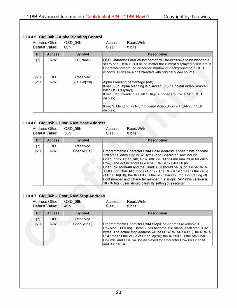
2.10.4.5 Cfg_04h – Alpha Blending Control Address Offset: OSD_04h Access: Read/Write Default Value: 00h Size: 8 bits
Bit Access Symbol Description [7] R/W FG_NoAB OSD Character ForeGround portion will be exclusive to be blended if
set to one. Default is 0 as no matter the current displayed pixels are in Character foreground or border/shadow or background or in OSD window, all will be alpha blended with original Video source.
[6:3] RO Reserved [2:0] R/W AB_Set[2:0] Alpha Blending percentage (n/8).
If set 000b, alpha blending is disabled (0/8 * Original Video Source + 8/8 * OSD display); If set 001b, blending as 1/8 * Original Video Source + 7/8 * OSD display; . . . If set N, blending as N/8 * Original Video Source + (8-N)/8 * OSD display;
2.10.4.6 Cfg_05h – Char_RAM Base Address Address Offset: OSD_05h Access: Read/Write Default Value: 38h Size: 8 bits
Bit Access Symbol Description [7] RO Reserved
[6:0] R/W CharBA[6:0] Programmable Character RAM Base Address. Those 7 bits become 128 steps, each step is 32 Bytes (one Character Row include Char_Index, Char_Attr, Row_Attr; i.e. 30 column maximum for each Row). The actual address will be 0RR-RRRX-XXXX (in Char_Idx_Mode=0 and the CharBA[0] should be 0), or 0RR-RRRR-XXXX (for Char_Idx_mode=1 or 2). The RR-RRRR means the value of CharBA[6:0]; the X-XXXX is the nth Char Column. For trading off Font number and Character number in a single RAM (this version is 1Kx16 bits), user should carefully setting this register.
2.10.4.7 Cfg_06h – Char_RAM Stop Address Address Offset: OSD_06h Access: Read/Write Default Value: 40h Size: 8 bits
Bit Access Symbol Description [7] RO Reserved
[6:0] R/W CharEA[6:0] Programmable Character RAM Stop/End Address (Available if Revision ID >= 0h). Those 7 bits become 128 steps, each step is 32 bytes. The actual stop address will be 0RR-RRRX-XXXX (The RRRR-RRR means the value of CharEA[6:0]; the X-XXXX is the nth Char Column. and OSD will be displayed for Character Row >= CharBA and < CharEA.

T118B Advanced Information-Confidential P/N-T118B-Rev01 Copyright by Terawins, Inc.
24
2.10.4.8 Cfg_09h – Blinking Control Address Offset: OSD_09h Access: Read/Write Default Value: 0Ah Size: 8 bits
Bit Access Symbol Description [7] R/W En_Global_Blink Enable whole OSD Characters blinking if set to 1.
[6:4] RO Reserved [3:2] R/W BCLK[1:0] Blinking Frequency Select (internal 4x BCLK for Blinking State
Machine). Set 00b for Refresh Rate /16; 01b for 1/32; 10b for 1/64; 11b for 1/128.
[1:0] R/W Duty[1:0] For adjusting the blinking duty cycle, Set: 00b for Global Blink Off, i.e., 0% Background, 100% OSD. 01b for 25% Background, 75% OSD. 10b for 50% Background, 50% OSD. 11b for 75% Background, 25% OSD.
2.10.4.9 Cfg_0Ah – Bit_Map Window Size: Height Upper Bits Address Offset: OSD_0Ah Access: Read/Write Default Value: 00h Size: 8 bits
Bit Access Symbol Description [7:6] RO Reserved [5:4] R/W BMH[9:8] Bit Map Window Height Upper bits (only available in Bit_Map mode).
Please refer to OSD_0Ch for detail. User must be careful of the OSD RAM size limitation.
[3:2] R/W BMP_Height_xN [1:0] Bit Map Window Vertical Enlarge (only available in Bit_Map mode). Set 00b for 1 line per dot, 01b for 2 lines per dot, 10b for 3 lines per dot, 11b for 4 lines per dot.
[1:0] R/W BMP_Width_xN[1:0] Bit Map Window Horizontal Enlarge (only available in Bit_Map mode). Set 00b for 1 pixel per dot, 01b for 2 pixels per dot, 10b for 3 pixels per dot, 11b for 4 pixels per dot.
2.10.4.10 Cfg_0Bh – Bit_Map Window Size: Width Address Offset: OSD_0Bh Access: Read/Write Default Value: 0Ah Size: 8 bits
Bit Access Symbol Description [7:0] R/W BMW[7:0] Bit Map Window Width Lower bits (only available in Bit_Map mode
This register has 8 bits, i.e., 256 steps (value 00h is not valid), each step is 16 or 8 dots depends on Bit2PP (OSD_00h<5>) setting. When Bit2PP=0 (i.e., 1 bit/pixel), each step is 16 dots. When Bit2PP=1 (i.e., 2 bits/pixel), each step is 8 dots. User must be careful of the OSD RAM size limitation.
2.10.4.11 Cfg_0Ch – Bit_Map Window Size: Height Address Offset: OSD_0Ch Access: Read/Write Default Value: 66h Size: 8 bits
Bit Access Symbol Description [7:0] R/W BMH[7:0] Bit Map Window Height Lower bits (only available in Bit_Map mode).
This register combined with OSD_0Ah<5:4> and become 10 bits, i.e. 1024 height step: all 0 for reserved, 10’h001 for 1 line, 10’h3FF for 1023 lines. User must be careful of the OSD RAM size limitation.

T118B Advanced Information-Confidential P/N-T118B-Rev01 Copyright by Terawins, Inc.
25
2.10.4.12 Cfg_0Dh – Bit_Map Window Size: Height Address Offset: OSD_0Dh Access: Read/Write Default Value: 86h Size: 8 bits
Bit Access Symbol Description [7:3] R/W FontH[4:0] Font Height. Value >=1 [2:0] R/W FontW[3:1] Font WeigthX2. Value 3~7 = width 6, 8, .., 14; others = width 16
2.10.4.13 Cfg_0Eh – OSD Color LUT RAM Data Port Address Offset: OSD_0Eh Access: Write Only Default Value: XXh Size: 8 bits
Bit Access Symbol Description [7:0] R/W LUT_D[7:0] The data will be written to (or read from) OSD Color LUT RAM. After
each Read or Write access to LUT RAM, then the LUT address will be increased automatically.
Note: Whenever the Configuration Index is programmed from other index value to 0Eh, the OSD Color LUT RAM becomes access capable and the address pointer is reset to 1 (the starting byte). In other words, whenever the index value is programmed to non-0Eh value, the OSD Color LUT RAM can not be access, and the pointer always kept at 1.
Note: The order to fill LUT RAM is: 1. LUT[1]_Green/Blue 2. LUT[1]_0000b/Red 3. LUT[2]_Green/Blue 4. LUT[2]_0000b/Red 5. LUT[3]_Green/Blue 6. ---- 29. LUT[15]_Green/Blue 30. LUT[15]_0000b/Red 31. LUT[0]_Green/Blue (wrap to beginning) 32. LUT[0]_0000b/Red
33. LUT[1]_Green/Blue 34. LUT[1]_0000b/Red ---
2.10.4.14 Cfg_0Fh – OSD Color LUT RAM Data Port Address Offset: OSD_0Fh Access: Read/Write Default Value: 00h Size: 8 bits
Bit Access Symbol Description [7] RO Reserved [6] R/W FontW_Byte When font width = 6 or 8 (and only), this bit is optional for the font
RAM utilization. When clear to 0, fonts stored in RAM as font width >=10. When set to 1, fonts stored in RAM: Even-indexed fonts put at the high byte in RAM, and Odd-indexed fonts put at the low byte in RAM.
[5:4] RO Reserved [3:2] R/W Char_Idx_Mode[1:0] Character attribute/Index coding modes, 0 for original 2 bytes (256
index) mode. 1 for 1-byte (64 index) mode, 2 for 1-byte (32 index) mode, 3 for reserved.
[1:0] R/W CRAM_ByteAccess[1:0] OSD RAM access pointer behavior: 0X: Word (2-bytes) R/W; (Fonts, BMP, Character Menu) 10: Low byte only; 11: High byte only; (Character Menu)

T118B Advanced Information-Confidential P/N-T118B-Rev01 Copyright by Terawins, Inc.
26
2.10.5 Functional Description
2.10.5.1 Host Access OSD RAM
2.10.5.1.1 Writing Data The OSD RAM size is 1Kx16, i.e., 1K word with each word is 2 bytes. The host interface is 8-bit data width, so whenever the host writes 2 times (one for data low byte, the other for data high byte) then it becomes one write with 16-bit data to OSD RAM. The ORAM_D (OSD module base address + 04h) port when writing in the 1st/3rd/5th/7th ..times, it will latch lower byte of OSD RAM writing data when the host want to program Font or Character, Attribute, BMP values; and when writing 2nd/4th/6th/8th … times, it will use this 8bits data as high byte and write both two bytes to OSD RAM.
2.10.5.1.2 Reading Data Read back data in OSD RAM is disabled.
2.10.5.1.3 Access Address The OSD RAM access pointer is programmed by the host write access to ORAM_AL and ORAM_AH ports. The OSD RAM size is 1Kx16, so the pointer is required to cover 1K words, i.e., 11 address lines => A[10:0]. When the host read these ORAM_AL/ORAM_AH ports, the pointer value reflects the current OSD RAM accessing pointer.

T118B Advanced Information-Confidential P/N-T118B-Rev01 Copyright by Terawins, Inc.
27
2.10.5.2 OSD Displaying in Character Mode
Geometry
Character Mode
Main Manual
Color Size & Position
Contrast/Brightness
HORD[10:1]( x 2 pixels)
VERTD[10:0] ( x HSYNC lines)
Character Background color
Character Foreground color/Blinking
Visib area (original RGB)
Fontsstorehere
Char.storehere
(Index /Attribute)
Firs
t Row
Last
Row
CharEA[6:0] (Character Ending Address)
CharBA[6:0] (Character Begin Address)
OSD RAM(1K x 16)
Figure 2-14 OSD Character Mode

T118B Advanced Information-Confidential P/N-T118B-Rev01 Copyright by Terawins, Inc.
28
2.10.5.3 OSD LUT Color Mapping
1. Character Mode
Duplicate to High/Low nibble;
2. Bit_Map Mode1 Bit/Pixel mode: Color_0= transparent; Color_1= LUT[1]2 Bits/Pixel mode: Color_0= transparent; Color_1~3= LUT[1..3]
BlueGreenRed4567 01230123IntBGR
Color Value
0000100001001100001010100110111000011001010111010011101101111111
012345670123456701234567
16x12 RAM
4567Null
1. Char_Idx_Mode=0, FG[3:0] as Color_0= transparent; Color_1~15= LUT[1..15]BG[2:0] as Color_0= transparent; Color_1~7= LUT[2,4,..14]
2. Char_Idx_Mode=1, FG as Color_0= transparent; Color_1= depends on its Row_Attribute FG_C[3:0], thenredirect to transparent or LUT[1..15]BG as Color_0= transparent; Color_1= depends on its Row_Attribute BG_C[2:0],then redirect to transparent or LUT[2,4,..14]
3. Char_Idx_Mode=2, FG[1:0] as Color_0= transparent; Color_1~3= LUT[1..3]BG as Color_0= transparent; Color_1= depends on its Row_Attribute BG_C[2:0],then redirect to transparent or LUT[2,4,..14]
Figure 2-15 OSD Color Look Up Table

T118B Advanced Information-Confidential P/N-T118B-Rev01 Copyright by Terawins, Inc.
29
2.10.5.4 Programming Examples
2.10.5.4.1 Configuring OSD Function To access OSD configuration registers, write register index to port A0h, and read/write data from port A1h. For example, set :
IOW A0h, 05h ; point to OSD_05h (Char Base Address register). IOR A1h; ; get Char Base Address. IOW A0h, 06h ; point to OSD_06h (Char Stop Address register). IOW A1h, 3Eh; ; Set Char Stop Address of current menu.
2.10.5.4.2 Fill LUT RAM LUT RAM size is 16 (address) x 12 (width). For example, need to fill LUT RAM as: LUT_RAM[1]=F5Ah, …LUT_RAM[15]=EF0h
IOW A0h, 0Eh ; point to OSD_0Eh (LUT RAM Data port), this will let LUT RAM be ; access-able and pointer starts from 0h of LUT RAM. IOW A1h, 5Ah; ; fill Green = 0101b and Blue = 1010h in LUT_RAM[1]. IOW A1h, 0Fh; ; fill Red = 1111b in LUT_RAM[1]. ; after this write, h/w will increase LUT RAM address to 2 automatically . . . . . . . IOW A1h, F0h; ; fill Green = 1111b and Blue = 0000h in LUT_RAM[15]. IOW A1h, 0Eh; ; fill Red = 1110b in LUT_RAM[15]. ; after this write, h/w will increase LUT RAM address to 0 automatically IOW A0h, non-0Eh ; Disable LUT RAM programming.
2.10.5.4.3 Load Fonts to OSD RAM OSD RAM size is 1K (address: 000h ~ 3FFh) x 16 (width). Fonts storing starts from address 000h. For example, loading some fonts to OSD RAM as: Font[0] is a space (all zero), Font[1] is a character 2 with box, Font[14] is a graphic,..
IOW A2h, 00h ; set OSD RAM starting access address low byte. (bit [7:0] as A[7:0]) IOW A3h, 00h; ; set OSD RAM starting access address high byte. (bit [3:0] as A[11:8]) ; then the OSD RAM address pointer is set to 000h. IOW A4h, 00h; ; low byte of first row of Font[0]. IOW A4h, 00h; ; high byte of first row of Font[0], after this write, h/w will increase OSD ;RAM address to 1 automatically IOW A4h, 00h; ; low byte of 2nd row of Font[0]. IOW A4h, 00h; ; high byte of 2nd row of Font[0], after this write, h/w will increase OSD ;RAM address to 2 automatically . . . . . . . (for example, programmed font size is 18 (height) x 12 (width) IOW A4h, 00h; ; low byte of 18th (last) row of Font[0]. IOW A4h, 00h; ; high byte of 18th row of Font[0], after this write, h/w will increase OSD ;RAM address to 012h automatically IOW A4h, F0h; ; low byte of first row of Font[0]. (since font width is 12, the low bye bit[3:0] ; is no use) IOW A4h, FFh; ; high byte of first row of Font[0], after this write, h/w will increase OSD ;RAM address to 013h automatically . . . . . . . IOW A2h, 68h ; set OSD RAM starting access address low byte. (bit [7:0] as A[7:0]) IOW A3h, 01h; ; set OSD RAM starting access address high byte. (bit [3:0] as A[11:8]), ; then the OSD RAM address pointer is set to 168h = 14d * 18d. IOW A4h, 40h; ; low byte of first row of Font[14]. IOW A4h, A3h; ; high byte of first row of Font[14],

T118B Advanced Information-Confidential P/N-T118B-Rev01 Copyright by Terawins, Inc.
30
2.11 TCON
2.11.1 LCD Panel Pin Assignment In this section, we illustrate those pins connected to AU 7” TFT-LCD panel module in a T118B video
system.
Table 2-3 T118B Rotation Control and LCD Panel Scanning Direction L/R U/D STH STV Reg 0xE1 Scanning Direction 1 1 STH2 STV1 0xBC Down-to-up, left-to-right 1 0 STH2 STV2 0xF4 Up-to-down, left-to-right 0 1 STH1 STV1 0xA8 Down-to-up, right-to-left 0 0 STH1 STV2 0xE0 Up-to-down, right-to-left
au
STH2STHL
STH1STHR
STV
2S
TVL
STV
1S
TVR
Figure 2-16 Scanning Direction of AU 7” panel

T118B Advanced Information-Confidential P/N-T118B-Rev01 Copyright by Terawins, Inc.
31
2.11.2 TCON Timing T118B is designed for analog LCD panel. Each 24-bit color pixel must be converted into analog voltage
via built-in triple DACs. The table 2-1 shows a typical setting for AU 7” panel with 10-Mhz operation clock.
Table 2-4 T118B TCON Register Set (C8 =1Bh, C9=03, CA=03h) Reg Reg value Operation 0x20 0x21 Line-inverted Control 0x21 0x79 Polarity Control
0x23,0x22 0x022D Placement of OEH 0x24 0x0C Duration of OEH
0x26,0x25 0x024B Placement of POL 0x28,0x27 0x021C Placement of GCLK 0x2A,0x29 0x0029 Duration of GCLK
0x2B 0x01 Placement of STH 0x30 0x01 Enable Placement of STV
0x32,0x31 0x01FB Placement of GOE 0x34,0x33 0x0037 Duration of GOE
0x35 0x06 Placement of STV
STH1
OEH
GOE
GLKV
POL
1.22 us 8.28 us
5.4 us
4.18 us3.74 us
VR/G/B
ViDC2.5 v
ViA4.6 v
4.6 v
0.4 v
HS
DEHtotal
R/G/B
Figure 2-17 AU 7” TCON Timing Spec

T118B Advanced Information-Confidential P/N-T118B-Rev01 Copyright by Terawins, Inc.
32
The waveforms shown below illustrate TCON location counting. Each TCON signal’s placement and duration are allowed to program as alike as analog LCD panels require. On the figure 2-2, the pulse placement starts counting at the leading edge of DE. After placement counter meets the value we give to P1_27h,P1_28h, the duration counter starts to count until the duration meets P1_29h,P1_2Ah. All of location counting use LLCK as counter clock.
GCLK
HS
DEHtotal
P1_28h,P1_27h
Htotal
P1_2Ah,P1_29h
Figure 2-18 Location Counting of GCLK

T118B Advanced Information-Confidential P/N-T118B-Rev01 Copyright by Terawins, Inc.
33
3 Register Description Serial Bus Register Set Page 0
3.1 ADC Register Set
3.1.1 ADC Clamping Pulse Placement and Duration Address Offset: 04h Access: Read/Write Default Value: 00h Size: 8 bits
Bit Access Symbol Description [7:5] R/W STIPCLPL Clamping pulse placement [4:0] R/W STIPCLDU Clamping pulse duration
3.1.2 ADC Channel 0 Static Gain Address Offset: 07h Access: Read/Write Default Value: 80h Size: 8 bits
Bit Access Symbol Description [7:0] R/W ADCRSG This register can set a fixed gain for ADC channel 0 when static gain
control is enabled
3.1.3 ADC Channel 1 Static Gain Address Offset: 08h Access: Read/Write Default Value: 80h Size: 8 bits
Bit Access Symbol Description [7:0] R/W ADCGSG This register can set a fixed gain for ADC channel 1 when static gain
control is enabled
3.1.4 ADC ACR Channel Offset Address Offset: 0Ah Access: Read/Write Default Value: 60h Size: 8 bits
Bit Access Symbol Description [7:2] R/W ADC_ROFF ADC Channel 0 DC Offset Control [1:0] R/W RESERVED
3.1.5 ADC AY Channel Offset Address Offset: 0Bh Access: Read/Write Default Value: 60h Size: 8 bits
Bit Access Symbol Description [7:2] R/W ADC_GOFF ADC Channel 1 DC Offset Control [1:0] R/W RESERVED
3.1.6 ADC General Control Configuration Register Address Offset: 0Dh Access: Read/Write Default Value: 20h Size: 8 bits

T118B Advanced Information-Confidential P/N-T118B-Rev01 Copyright by Terawins, Inc.
34
Bit Access Symbol Description [7:6] R/W CLPMD Clamping mode
Mode Type
0 Fixed window1 Locked Window2 Reserved3 Reserved
[5] R/W DCEN DC Clamping Enable [4] R/W DCSEL Clamping Source Selection [3] R/W RESERVED
[2] R/W DC_CAL_RDY DC Calibration Ready [1] R/W DC_CALEN DC Calibration Enable [0] R/W DC_CALMD DC Calibration Mode
Mode Type0 minimum1 average
3.1.7 ADC Power Down Control Address Offset: 0Fh Access: Read/Write Default Value: 00h Size: 8 bits
Bit Access Symbol Description [7:6] R/W RESERVED [5] R/W PD1 1: Power down
0: Power up [4] R/W PD0 1: Power down
0: Power up [3:0] R/W RESERVED
3.1.8 YPbPr Clamping Control Register Address Offset: 11h Access: Read/Write Default Value: 00h Size: 8 bits
Bit Access Symbol Description [7:6] R/W GMIDSEL Clamping Voltage
Mode Voltage Type0 Adaptiv Voltage1 0.65*Ref2 0.5*Ref3 0.35*Ref

T118B Advanced Information-Confidential P/N-T118B-Rev01 Copyright by Terawins, Inc.
35
[5:4] R/W RMIDSEL Clamping Voltage Mode Voltage Type
0 Adaptiv Voltage1 0.65*Ref2 0.5*Ref3 0.35*Ref
[3] R/W ADSHARE2 0: Take sampled data from channel 2 and channel 4 (used for CbCr) 1: Take sampled data from channel 2 or channel 4
[2] R/W ADSHARE1 0: Take sampled data from channel 1 and channel 3 (used for CbCr) 1: Take sampled data from channel 1 or channel 3
[1] R/W GSCALE ADC Channel 2 Clamping Mode Mode Select
0 Clamp to ground1 Clamp to midscale
[0] R/W RSCALE ADC Channel 1 Clamping Mode Mode Type
0 Clamp to ground1 Clamp to midscale
3.1.9 Analog Source MUX Selection Address Offset: 18h Access: Read/Write Default Value: 00h Size: 8 bits
Bit Access Symbol Description [7:6] R/W AI4SEL Analog mux selection for channel 2 ADC
AI4SEL=00: Channel 4 input signal is from GND AI4SEL=01: Channel 4 input signal is from GND AI4SEL=1x: Channel 4 input signal is from GND
[5:4] R/W AI3SEL Analog mux selection for channel 1 ADC AI3SEL=00: Channel 4 input signal is from ACB0 AI3SEL=01: Channel 4 input signal is from ACB1 AI3SEL=1x: Channel 4 input signal is from GND
[3:2] R/W AI2SEL Analog mux selection for channel 2 ADC AI2SEL=00: Channel 4 input signal is from AY0 AI2SEL=01: Channel 4 input signal is from AY1 AI2SEL=1x: Channel 4 input signal is from GND
[1:0] R/W AI1SEL Analog mux selection for channel 1 ADC AI3SEL=00: Channel 4 input signal is from ACR0 AI3SEL=01: Channel 4 input signal is from ACR1 AI3SEL=1x: Channel 4 input signal is from GND
3.1.10 Y/Cb/Cr Data Switching Control Address Offset: 19h Access: Read/Write Default Value: 07h Size: 8 bits
Bit Access Symbol Description

T118B Advanced Information-Confidential P/N-T118B-Rev01 Copyright by Terawins, Inc.
36
Bit Access Symbol Description [7] R/W INSEL2 ADC input mux selection
0: Channel 2 ADC takes data from channel 2 (AY) 1: Channel 2 ADC takes data from channel 4 (GND)
[6] R/W INSEL1 0: Channel 1 ADC takes data from channel 1 (ACR) 1: Channel 1 ADC takes data from channel 3 (ACB)
[5:4] R/W CBINSEL CB input selection 0: Channel 1 1: Channel 2 2: Channel 3 3: Channel 4
[3:2] R/W YINSEL Y/Luma input selection 0: Channel 1 1: Channel 2 2: Channel 3 3: Channel 4
[1:0] R/W CRINSEL S-video Chroma or CR input selection 0: Channel 1 1: Channel 2 2: Channel 3 3: Channel 4
3.1.11 ADC Analog AGC Selection Address Offset: 1Ah Access: Read/Write Default Value: 42h Size: 8 bits
Bit Access Symbol Description [7:6] R/W AGC_GAINMD
Mode Type0 Positive gain1 Positive gain 1x~2x2 Negative gain 1x~2x3 Negative gain
[5] R/W AGC_FreeMM 1: release dynamic gain control whenever no signal is present 0: allow dynamic gain control
[4:2] R/W RESERVED [1] R/W Y_AGC_SEL If 0, refer to ADCGSG
Mode Type0 Static gain1 Dynamic gain
[0] R/W CR_AGC_SEL If 0, refer to ADCRSG Mode Type
0 Static gain1 Dynamic gain
3.1.12 Blank Sync Level Address Offset: 1Ch Access: Read/Write Default Value: C0h Size: 8 bits
Bit Access Symbol Description [7:0] R/W BLANK_SL

T118B Advanced Information-Confidential P/N-T118B-Rev01 Copyright by Terawins, Inc.
37
3.1.13 ADC Read-back Selection Address Offset: 1Dh Access: Read/Write Default Value: 80h Size: 8 bits
Bit Access Symbol Description [7:3] R/W RESERVED [2:0] R/W RBK_SEL 1: Read Max of ADC data
0:Read Min of ADC data or Average of ADC data
3.1.14 ADC Read-back Data Address Offset: 1Eh Access: Read/Write Default Value: 00h Size: 8 bits
Bit Access Symbol Description [7:0] R/W RBK_ADC[7:0]
3.1.15 ADC Read-back Data Address Offset: 1Fh Access: Read/Write Default Value: 00h Size: 8 bits
Bit Access Symbol Description [7:2] R RESERVED [1:0] R RBK_ADC[9:0]
3.1.16 De-Interlaced Process & Vertical Shadow Control Register Address Offset: 30h Access: Read/Write Default Value: 82h Size: 8 bits
Bit Access Symbol Description [7] R/W CBCR_INTERP 1: Enable CbCr interpolation
0: Disable [6] R/W BLANK_LF_PRSVC 1:When Left Cropping and this bit are enabled, the original
YCbCr are preserved on blank interval. 0: When Left Cropping, the original YCbCr are reset as blank color
[5] R/W VST_CHGSEL 1:Vsync timing change determined by 8*# of XCLK 0:Vsynnc timing change determined by # of hsync # can be assigned at Reg 0x3A
[4] R/W INT_EDGE Interrupt polarity 1: positive 0: negative
[3] R/W LB_SIZE_FIXED This bit control capture size for Scaler. 1: Hsize and Vsize are assigned by 54h ~57h 0: sizes assigned by input sources.
[2] R/W ENQKHS Set 0 for normal operation [1] R/W ITLCPRO Set 1 for interlaced video
Set 0 for non-interlaced video [0] R/W RESERVED

T118B Advanced Information-Confidential P/N-T118B-Rev01 Copyright by Terawins, Inc.
38
3.1.17 Source Select Register Address Offset: 31h Access: Read/Write Default Value: 00h Size: 8 bits
Bit Access Symbol Description [7:5] R/W RESERVED [4] R/W RESERVED
[3:0] R/W RESERVED
3.1.18 Interrupt Status Register Address Offset: 32h Access: Read/Write Default Value: 00h Size: 8 bits
Bit Access Symbol Description [7] R/W RESERVED [6] R ITLCFLM Indicates incoming video signal is interlaced
[5:0] R/W INTSTS
3.1.19 Interrupt Mask Register Address Offset: 33h Access: Read/Write Default Value: FFh Size: 8 bits
Bit Access Symbol Description [7:6] R/W RESERVED [5:0] R/W INTMASK
3.1.20 Lower 8-bit Timer Counter Register Address Offset: 35h Access: Read/Write Default Value: 00h Size: 8 bits
Bit Access Symbol Description [7:0] R/W TM_1MS_L [7:0] Lower byte of the number of XCLK’s in 1ms.
3.1.21 Upper 8-bit Timer Counter Register Address Offset: 36h Access: Read/Write Default Value: 10h Size: 8 bits
Bit Access Symbol Description [7:0] R/W TM_1MS_H [15:8] Higher byte of the number of XCLK’s in 1ms.
3.1.22 VSYNC Missing Counter Register Address Offset: 37h Access: Read/Write Default Value: 40h Size: 8 bits
Bit Access Symbol Description [7:0] R/W V_MISS_CNT
3.1.23 Lower 8-bit HSYNC Missing Counter Register Address Offset: 38h Access: Read/Write Default Value: 00h Size: 8 bits
Bit Access Symbol Description [7:0] R/W H_MISS_CNT_L[7:0]

T118B Advanced Information-Confidential P/N-T118B-Rev01 Copyright by Terawins, Inc.
39
3.1.24 Upper 8-bit HSYNC Missing Counter Register Address Offset: 39h Access: Read/Write Default Value: 10h Size: 8 bits
Bit Access Symbol Description [7:0] R/W H_MISS_CNT_L[15:8]
3.1.25 VSYNC Delta Difference Result Register Address Offset: 3Ah Access: Read/Write Default Value: 00h Size: 8 bits
Bit Access Symbol Description [7:0] R/W VSYNC_DLT[7:0]
3.1.26 HSYNC Delta Difference Result Register Address Offset: 3Bh Access: Read/Write Default Value: 00h Size: 8 bits
Bit Access Symbol Description [7:0] R/W HSYNC_DLT[7:0]
3.1.27 Input Sync Signal Detection Register Address Offset: 3Fh Access: Read/Write Default Value: 00h Size: 8 bits
Bit Access Symbol Description [7] R/W HSTLSPVS 1:use trailing edge of hsync to sample
0:use leading edge of hsync to sample [6] R/W AUTOVSD6 When the edges of vsync and hsync are too close, input detection
circuit can delay vsync 6 cycle of XCLK to avoid unstable detection 1:Automatically delay 6 cycles of XCLK if CFSEEDGE is true. 0:Dealy 6 cycles of XCLK if FCVSD6 is true
[5] R/W FCVSD6 AUTOVSD6 FCSVSD6T
1 x Auomatically delay VSync 6 XCLK if CFSEEDGE is true
0 1 Force to delay VSync 6 XCLK
0 0 No Vsync Dealy
[4] R CFSEEDGE VS and HS edges are to close. [3:2] R/W RESERVED [1] R/W VsHs_Sync_Edge 1: leading edge of Vsi
0: falling edge of His [0] R/W VsHS_Sync_En 1:leading edge of Vsi starts at leading edge of Hsi
0:leading edge of Vsi starts at mid of Hsi

T118B Advanced Information-Confidential P/N-T118B-Rev01 Copyright by Terawins, Inc.
40
3.1.28 Left Border Cropping Address Offset: 40h Access: Read/Write Default Value: 00h Table 3-35 Left Border Croping
Bit Access Symbol Description [7:6] R/W RESERVED [5:0] R/W CROP_LEFTB Remove noisy pixels appearing on left border.
1LSB =1 pixel
3.1.29 Gamma Correction for Video Source Address Offset: 42h Access: Read/Write Default Value: 00h Size: 8 bits
Bit Access Symbol Description [7:6] R/W VG_SEL 0: Both Y ans C
1:C 2:Y 3:Reserved
[5:2] R/W RESERVED [1] R/W VGAM_EN Enable Video gamma correction [0] R/W RESERVED
3.1.30 Video Gamma Address Port Register Address Offset: 43h Access: Read/Write Default Value: 00h Size: 8 bits
Bit Access Symbol Description [7:0] R/W VGAM_ADR Video gamma coefficient table address. The Index range is 00h~FFh
3.1.31 Video Gamma Write/Read Port Register Address Offset: 44h Access: Read/Write Default Value: 00h Size: 8 bits
Bit Access Symbol Description [7:0] R/W VGA_WR_D Video gamma coefficient write data port.
3.1.32 VSYNC Timing Measurement Register Address Offset: 50h Access: Read/Write Default Value: 00h Size: 8 bits
Bit Access Symbol Description [7] R/W RESERVED [6] R/W HSPMD Register 0x5c and 0x5d can be HS pulse width or hsync period
1:Period in # of pixel clock. 0:Hsync pulse width in # of pixel clock.
[5] R DONE_FRMXCLKCNT When EN_FRAMEXCLKCNT is enabled, a whole frame time can be obtained through XCLK counting. See registers 0x51, 0x52 and 0x53. After this bit read back as 1, then clear EN_FRAMEXCLKCNT first before reading 0x51~0x53 values.
[4] R/W EN_FRAMEXCLKCNT When input VSync changes, enable this bit to start measurement on VSync using XCLK.
[3:0] R/W RESERVED

T118B Advanced Information-Confidential P/N-T118B-Rev01 Copyright by Terawins, Inc.
41
3.1.33 VSYNC Measurement Counter L Register Address Offset: 51h Access: Read/Write Default Value: 00h Size: 8 bits
Bit Access Symbol Description [7:0] R/W FRMXCLK_SUM[7:0]
3.1.34 VSYNC Measurement Counter M Register Address Offset: 52h Access: Read Only Default Value: 00h Size: 8 bits
Bit Access Symbol Description [7:0] R/W FRMXCLK_SUM[15:8]
3.1.35 VSYNC Measurement Counter H Register Address Offset: 53h Access: Read Only Default Value: 00h Size: 8 bits
Bit Access Symbol Description [7:0] R/W FRMXCLK_SUM[23:16]
3.1.36 Hsize Address Offset: 54h Access: Read Only Default Value: 00h Size: 8 bits
Bit Access Symbol Description [7:0] R HSIZE[7:0]
3.1.37 Hsize Address Offset: 55h Access: Read Only Default Value: 00h Size: 8 bits
Bit Access Symbol Description [7:4] R/W RESERVED [3:0] R HSIZE[11:8]
3.1.38 Vsize Address Offset: 56h Access: Read Only Default Value: 00h Size: 8 bits
Bit Access Symbol Description [7:0] R VSIZE[7:0]
3.1.39 Vsize Address Offset: 57h Access: Read Only Default Value: 00h Size: 8 bits
Bit Access Symbol Description [7:4] R/W RESERVED [3:0] R VSIZE[11:8]
T118B Advanced Information-Confidential P/N-T118B-Rev01 Copyright by Terawins, Inc.
42
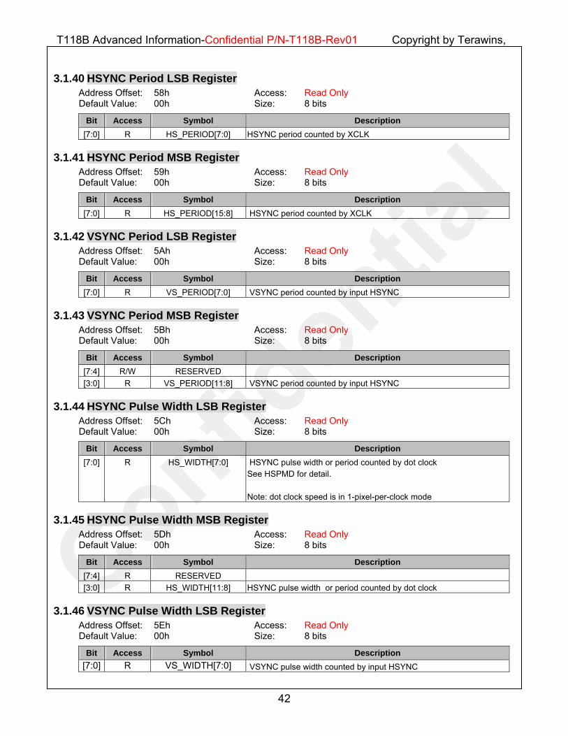
3.1.40 HSYNC Period LSB Register Address Offset: 58h Access: Read Only Default Value: 00h Size: 8 bits
Bit Access Symbol Description [7:0] R HS_PERIOD[7:0] HSYNC period counted by XCLK
3.1.41 HSYNC Period MSB Register Address Offset: 59h Access: Read Only Default Value: 00h Size: 8 bits
Bit Access Symbol Description [7:0] R HS_PERIOD[15:8] HSYNC period counted by XCLK
3.1.42 VSYNC Period LSB Register Address Offset: 5Ah Access: Read Only Default Value: 00h Size: 8 bits
Bit Access Symbol Description [7:0] R VS_PERIOD[7:0] VSYNC period counted by input HSYNC
3.1.43 VSYNC Period MSB Register Address Offset: 5Bh Access: Read Only Default Value: 00h Size: 8 bits
Bit Access Symbol Description [7:4] R/W RESERVED [3:0] R VS_PERIOD[11:8] VSYNC period counted by input HSYNC
3.1.44 HSYNC Pulse Width LSB Register Address Offset: 5Ch Access: Read Only Default Value: 00h Size: 8 bits
Bit Access Symbol Description [7:0] R HS_WIDTH[7:0] HSYNC pulse width or period counted by dot clock
See HSPMD for detail. Note: dot clock speed is in 1-pixel-per-clock mode
3.1.45 HSYNC Pulse Width MSB Register Address Offset: 5Dh Access: Read Only Default Value: 00h Size: 8 bits
Bit Access Symbol Description [7:4] R RESERVED [3:0] R HS_WIDTH[11:8] HSYNC pulse width or period counted by dot clock
3.1.46 VSYNC Pulse Width LSB Register Address Offset: 5Eh Access: Read Only Default Value: 00h Size: 8 bits
Bit Access Symbol Description [7:0] R VS_WIDTH[7:0] VSYNC pulse width counted by input HSYNC

T118B Advanced Information-Confidential P/N-T118B-Rev01 Copyright by Terawins, Inc.
43
3.1.47 VSYNC Pulse Width MSB Register Address Offset: 5Fh Access: Read Only Default Value: 00h Size: 8 bits
Bit Access Symbol Description [7:4] R RESERVED [3:0] R VS_WIDTH[11:8] VSYNC pulse width counted by input HSYNC

T118B Advanced Information-Confidential P/N-T118B-Rev01 Copyright by Terawins, Inc.
44
3.2 Picture Enhancement Register Set
3.2.1 Bandwidth of Digital Color Transient Improvement Address Offset: 60h Access: Default Value: 02h Size: 8 bits
Bit Access Symbol Description [7] R/W DCTI_EC DCTI Error Correction
[6:1] R/W RESERVED [0] R/W DCTI_BW 0: high bandwidth
1: low bandwidth
3.2.2 Luma Peaking Control Address Offset: 61h Access: Default Value: 08h Size: 8 bits
Bit Access Symbol Description [7] R/W PeakingEN [6] R/W HoldLR_PIX When this bit is enabled, the peaking doesn’t affect pixels appearing
at Left/Right borders. [5:0] R/W PeakingCo
3.2.3 Bandpass Peaking Coef Address Offset: 62h Access: Default Value: 04h Size: 8 bits
Bit Access Symbol Description [7:5] R/W RESERVED [4:0] R/W BP_COEF
3.2.4 Highpass Peaking Coef Address Offset: 63h Access: Default Value: 04h Size: 8 bits
Bit Access Symbol Description [7:5] R/W RESERVED [4:0] R/W HP_COEF
3.2.5 Lowpass Peaking Coef Address Offset: 64h Access: Default Value: 02h Size: 8 bits
Bit Access Symbol Description [7:3] R/W RESERVED [2:0] R/W LP_COEF
3.2.6 Gain and Coring of DLTI Address Offset: 65h Access:

T118B Advanced Information-Confidential P/N-T118B-Rev01 Copyright by Terawins, Inc.
45
Default Value: 08h Size: 8 bits
Bit Access Symbol Description [7:5] R/W DLTI_GAIN [4:0] R/W DLTI_CO
3.2.7 Gain and Coring of DCTI Address Offset: 66h Access: Default Value: 08h Size: 8 bits
Bit Access Symbol Description [7:5] R/W DCTI_GAIN [4:0] R/W DCTI_CO
3.2.8 Contrast Adjust Address Offset: 68h Access: Default Value: 80h Size: 8 bits
Bit Access Symbol Description [7:0] R/W LumaCON
3.2.9 Brightness Adjust Address Offset: 69h Access: Default Value: 80h Size: 8 bits
Bit Access Symbol Description [7:0] R/W LumaBRI
3.2.10 Hue Sin Adjust Address Offset: 6Ah Access: Default Value: 00h Size: 8 bits
Bit Access Symbol Description [7:0] R/W HueSin
3.2.11 Hue Cos Adjust Address Offset: 6Bh Access: Default Value: 7Fh Size: 8 bits
Bit Access Symbol Description [7:0] R/W HueCos
3.2.12 Chroma Saturation Adjust Address Offset: 6Ch Access: Default Value: 80h Size: 8 bits
Bit Access Symbol Description [7:0] R/W ChromSat

T118B Advanced Information-Confidential P/N-T118B-Rev01 Copyright by Terawins, Inc.
46
3.3 Scaling Register Set
3.3.1 Scaling General Control Register
Address Offset: 70h Access: Read/Write Default Value: 00h Size: 8 bits
Bit Access Symbol Description [7:6] R/W RESERVED [5] R/W Inv_VideoF Inv_VideoF: Reverse input odd field control for intra field
scaling, only take action when ITLCPRO is set to 1. [4] R/W Dclki_is_Faster Software need to turn this bit on when the freq of input pixel clock is
higher than output pixel clock. [3:2] R/W De-interlacing option 00:1/2 line
01:1/4 line 10: 1/8 line
[0] R/W C16_Pointer_RST Reset coef table. 1: Reset write pointer to 0x00. 0: Don’t Care
3.3.2 Scaling Coefficient Data Port Register Address Offset: 71h Access: Read/Write Default Value: 00h Size: 8 bits
Bit Access Symbol Description [7:0] R/W Coef_Data_Port
3.3.3 Horizontal Scale Step LSB Register Address Offset: 72h Access: Read/Write Default Value: 00h Size: 8 bits
Bit Access Symbol Description [7:0] R/W H_Scale_Step [7:0]
3.3.4 Horizontal Scale Step MSB Register Address Offset: 73h Access: Read/Write Default Value: 00h Size: 8 bits
Bit Access Symbol Description [7:0] R/W H_Scale_Step [15:8]
3.3.5 Vertical Scale Step LSB Register Address Offset: 74h Access: Read/Write Default Value: 00h Size: 8 bits
Bit Access Symbol Description [7:0] R/W V_Scale_Step [7:0]

T118B Advanced Information-Confidential P/N-T118B-Rev01 Copyright by Terawins, Inc.
47
3.3.6 Vertical Scale Step MSB Register Address Offset: 75h Access: Read/Write Default Value: 00h Size: 8 bits
Bit Access Symbol Description [7:0] R/W V_Scale_Step [15:8]
3.3.7 Horizontal Aspect Ratio Register Address Offset: 76h Access: Read/Write Default Value: 00h Size: 8 bits
Bit Access Symbol Description [7:0] R/W HASPR[7:0]
3.3.8 Horizontal Aspect Ratio Register Address Offset: 77h Access: Read/Write Default Value: 00h Size: 8 bits
Bit Access Symbol Description [7] R/W HASPEN [6] R/W HASP_C_ELG
[5:0] R/W HASPR[13:8]
3.3.9 Antialiasing Filtering Address Offset: 78h Access: Read/Write Default Value: 00h Size: 8 bits
Bit Access Symbol Description [7:6] R/W RESERVED [5:4] R/W LPF_AVE 3: LPF ==[0.25 0.25 0.25 0.25]
2: LPF ==[0.25 0.5 0.25] 0/1:LPF ==[0 1 0]
[3] R/W LPF_BND_DUP Padding starting and ending pixels at starting and ending position. [2] R/W RESERVED
[1:0] R/W LPF_SHPIX Pipelined alignment for antialiasing LPF
3.3.10 Half Sampling and Luma High Boost Address Offset: 79h Access: Read/Write Default Value: 00h Size: 8 bits
Bit Access Symbol Description [7:6] R/W RESERVED [5] R/W En_Half_Input Half Sampling by pixel reduction. When this bit is enabled, P0_30h[7]
must be disabled. [4] R/W RESERVED
[3:0] R/W LumaHB[3:0] Luma High Boost Coef
3.3.11 Chroma High Boost Address Offset: 7Ah Access: Read/Write Default Value: 00h Size: 8 bits
Bit Access Symbol Description [7:4] R/W RESERVED [3:0] R/W ChromaHB[3:0] Chroma High Boost Coef

T118B Advanced Information-Confidential P/N-T118B-Rev01 Copyright by Terawins, Inc.
48
3.3.12 Luma High Boost Address Offset: 7Bh Access: Read/Write Default Value: 00h Size: 8 bits
Bit Access Symbol Description [7:0] R/W YDrTh Edge threshold value for 2nd derivative of Luma
3.3.13 Chroma High Boost Address Offset: 7Ch Access: Read/Write Default Value: 00h Size: 8 bits
Bit Access Symbol Description [7:0] R/W CDrTh Edge threshold value for 2nd derivative of Chroma
3.3.14 Scaler Frame Color Y Address Offset: 7Dh Access: Read/Write Default Value: 10h Size: 8 bits
Bit Access Symbol Description [7:0] R/W SCFR_Y
3.3.15 Scaler Frame Color Cb Address Offset: 7Eh Access: Read/Write Default Value: 80h Size: 8 bits
Bit Access Symbol Description [7:0] R/W SCFR_Cb
3.3.16 Scaler Frame Color Cr Address Offset: 7Fh Access: Read/Write Default Value: 80h Size: 8 bits
Bit Access Symbol Description [7:0] R/W SCFR_Cr
3.3.17 Input Vsync Leading Edge to DE Time Counter 1/3 Register Address Offset: 81h Access: Read/Write Default Value: 00h Size: 8 bits
Bit Access Symbol Description [7:0] R TVIBLK[7:0] Timing counter can measure the time interval between leading edge
of input vsync and first valid input pixel. This time interval is TVIBLK * (1/XCLK )
3.3.18 Input Vsync Leading Edge to DE Time Counter 2/3 Register Address Offset: 82h Access: Read/Write Default Value: 00h Size: 8 bits
Bit Access Symbol Description [7:0] R TVIBLK [15:8]

T118B Advanced Information-Confidential P/N-T118B-Rev01 Copyright by Terawins, Inc.
49
3.3.19 Input Vsync Leading Edge to DE Time Counter 3/3 Register Address Offset: 83h Access: Read/Write Default Value: 00h Size: 8 bits
Bit Access Symbol Description [7:0] R/W TVIBLK[23:16]
3.3.20 Line Buffer Configuration LSB Register Address Offset: 84h Access: Read/Write Default Value: 00h Size: 8 bits
Bit Access Symbol Description [7:0] R/W LBPRFL[7:0] LBPRFL can cause a time dealy in XCLK count between the leading
edge of input Vsync and leading edge of output Vsync.
3.3.21 Line Buffer Configuration MSB Register Address Offset: 85h Access: Read/Write Default Value: 00h Size: 8 bits
Bit Access Symbol Description [7:0] R/W LBPRFL[15:8]
3.3.22 Output Hsync Vibration Step Register Address Offset: 86h Access: Read/Write Default Value: 00h Size: 8 bits
Bit Access Symbol Description [7:0] R/W HSVIB Output HSync re-map factor in vertical Active period.
3.3.23 Output Vsync Front Porch Remapping Register Address Offset: 87h Access: Read/Write Default Value: 00h Size: 8 bits
Bit Access Symbol Description [7:0] R/W VSFPRMP Output HSync remap amount in vertical front porch period.
3.3.24 Left Display Border Configuration Register Address Offset: 88h Access: Read/Write Default Value: 00h Size: 8 bits
Bit Access Symbol Description [7:0] R/W HLDSPLB[7:0] When Output pixel’s index is less than HRDSPLB, output pixel value
is assigned as left display border FMCLRRDE, FMCLRGRN , FMCLRBLU
3.3.25 Left Display Border Configuration Register Address Offset: 89h Access: Read/Write Default Value: 00h Size: 8 bits
Bit Access Symbol Description [7] R/W HDSPLB_INV Horizontal border is on if HDSPLB_INV is set as follows
1: HLDSPLB < Horizontal border < HRDSPLB 0: Horizontal border < HLDSPLB or HRDSPLB < Horizontal border

T118B Advanced Information-Confidential P/N-T118B-Rev01 Copyright by Terawins, Inc.
50
Bit Access Symbol Description [6] R/w VDSPLB_INV Vertical border is on if VDSPLB_INV is set as follows
1: VTDSPLB < < VBDSPLB 0: Vertical border < VTDSPLB or VBDSPLB < Vertical border
[5] R/W HDSPLB_STY Border style 1: mesh 0: solid
[4] R/W VDSPLB_STY Border style 1: mesh 0: solid
[3:0] R/W HLDSPLB[11:8]
3.3.26 Right Display Border Configuration LSB Register Address Offset: 8Ah Access: Read/Write Default Value: 00h Size: 8 bits
Bit Access Symbol Description [7:0] R/W HRDSPLB[7:0] When Output pixel’s index is greater than HRDSPLB, output pixel
value is assigned as right display border FMCLRRDE, FMCLRGRN , FMCLRBLU
3.3.27 Right Display Border Configuration MSB Register Address Offset: 8Bh Access: Read/Write Default Value: 00h Size: 8 bits
Bit Access Symbol Description [7:4] R/W RESERVED [3:0] R/W HRDSPLB[11:8]
3.3.28 Top Display Border Configuration LSB Register Address Offset: 8Ch Access: Read/Write Default Value: 00h Size: 8 bits
Bit Access Symbol Description [7:0] R/W VTDSPLB[7:0]
3.3.29 Top Display Border Configuration MSB Register Address Offset: 8Dh Access: Read/Write Default Value: 00h Size: 8 bits
Bit Access Symbol Description [7:6] R/W HDSPLB_GRID[1:0] H grip precision,
00b: 1 pixel 01b: 4 pixels 10b: 16 pixels 11b: 32 pixels
[5:4] R/W VDSPLB_GRID[1:0] V grip precision 00b: 1 line 01b: 4 lines 10b: 16 lines 11b: 32 lines
[3:0] R/W VTDSPLB[11:8]

T118B Advanced Information-Confidential P/N-T118B-Rev01 Copyright by Terawins, Inc.
51
3.3.30 Bottom Display Border Configuration LSB Register Address Offset: 8Eh Access: Read/Write Default Value: 00h Size: 8 bits
Bit Access Symbol Description [7:0] R/W VBDSPLB[7:0]
3.3.31 Bottom Display Border Configuration MSB Register Address Offset: 8Fh Access: Read/Write Default Value: 00h Size: 8 bits
Bit Access Symbol Description [7:4] R/W RESERVED [3:0] R/W VBDSPLB[11:8]
T118B Advanced Information-Confidential P/N-T118B-Rev01 Copyright by Terawins, Inc.
52
3.4 Color Space Converter Register Set
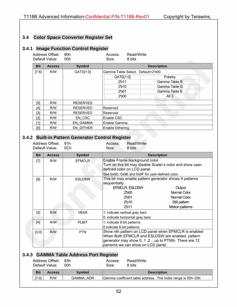
3.4.1 Image Function Control Register Address Offset: 90h Access: Read/Write Default Value: 00h Size: 8 bits
Bit Access Symbol Description [7:6] R/W GATS[1:0] Gamma Table Select. Default=2’b00.
GATS[1:0] Polarity2'b11 Gamma Table R2'b10 Gamma Table G2'b01 Gamma Table B2'b00 All 3
[5] R/W RESERVED [4] R/W RESERVED Reserved [3] R/W RESERVED Reserved [2] R/W EN_CSC Enable CSC [1] R/W EN_GAMMA Enable Gamma. [0] R/W EN_DITHER Enable Dithering.
3.4.2 Built-in Pattern Generator Control Register Address Offset: 91h Access: Read/Write Default Value: 0Ch Size: 8 bits
Bit Access Symbol Description [7] R/W EFMCLR Enable Frame background color
Turn on this bit may disable Scaler’s color and show user-defined color on LCD panel. See 0x9D, 0x9E and 0x9F for user-defined color.
[6] R/W ESLDSW This bit may enable pattern generator shows 9 patterns sequentially.
EFMCLR, ESLDSW Output2'b00 Normal Color2'b01 Normal Color2'b10 Still pattern2'b11 Motion patterns
[5] R/W VBAR 1: indicate vertical gray bars 0: indicate horizontal gray bars
[4] R/W PLBIT 1: indicate 8-bit patterns 0:indicate 6-bit patterns
[3:0] R/W PTN Show nth pattern on LCD panel when EFMCLR is enabled When Both EFMCLR and ESLDSW are enabled, pattern generator may show 0, 1 ,2 ...up to PTNth. There are 12 parrerns we can show on LCD panel.
3.4.3 GAMMA Table Address Port Register Address Offset: 93h Access: Read/Write Default Value: 00h Size: 8 bits
Bit Access Symbol Description [7:0] R/W GAMMA_ADR Gamma coefficient table address. The Index range is 00h~20h

T118B Advanced Information-Confidential P/N-T118B-Rev01 Copyright by Terawins, Inc.
53
3.4.4 GAMMA Table Write Data Port Register Address Offset: 94h Access: Read/Write Default Value: 00h Size: 8 bits
Bit Access Symbol Description [7:0] R/W GAMMA_WR_D Gamma coefficient write data port.
3.4.5 Black Level Expansion Threshold Address Offset: 95h Access: Read/Write Default Value: 10h Size: 8 bits
Bit Access Symbol Description [7:0] R/W BLE_TH
3.4.6 VIP Black level Expansion Gain / Offset Control Register Address Offset: 96h Access: Read/Write DefaultValue: 00h Size: 8 bits
Bit Access Symbol Description [7:4] R/W BLE_GAIN [3:2] R/W RESERVED [1:0] R/W BLE_OFFSET
3.4.7 CSC Y Coef Address Offset: 97h Access: Read/Write Default Value: 95h Size: 8 bits
Bit Access Symbol Description [7:0] R/W YCoefCSC 1.7-bit fixed point
3.4.8 CSC Red Coef of Cr Address Offset: 98h Access: Read/Write Default Value: CCh Size: 8 bits
Bit Access Symbol Description [7:0] R/W CrCoef_R 1.7-bit fixed point
3.4.9 CSC Green Coef of Cb Address Offset: 99h Access: Read/Write Default Value: 64h Size: 8 bits
Bit Access Symbol Description [7:0] R/W CbCoef_G 0.8-bit fixed point
3.4.10 CSC Green Coef of Cr Address Offset: 9Ah Access: Read/Write Default Value: D0h Size: 8 bits
Bit Access Symbol Description [7:0] R/W CrCoef_G 0.8-bit fixed point

T118B Advanced Information-Confidential P/N-T118B-Rev01 Copyright by Terawins, Inc.
54
3.4.11 CSC Blue Coef of Cb Address Offset: 9Bh Access: Read/Write Default Value: 81h Size: 8 bits
Bit Access Symbol Description [7:0] R/W CbCoef_B 2.6-bit fixed point
3.4.12 Pattern Color Gradient & Dithering Mode Register Address Offset: 9Ch Access: Read/Write Default Value: 00h Size: 8 bits
Bit Access Symbol Description [7:4] R/W CLRGRDT[3:0] When both ESLDSW and EFMCLR are enabled, CLRGRDT may set
color gradient at pattern 2, 3 ,4, 5 [3:2] R/W RESERVED [1:0] R/W DITHER_MD Dithering mode. It is enabled by register 90h.
DITHER_MD Output2'b00 4-bit output2'b01 5-bit output2'b10 6-bit output2'b11 7-bit output
3.4.13 Frame Color Red Configuration Register Address Offset: 9Dh Access: Read/Write Default Value: 00h Size: 8 bits
Bit Access Symbol Description [7:0] R/W FMCLRRDE 8 bits of red color depth for frame color.
3.4.14 Frame Color Green Configuration Register Address Offset: 9Eh Access: Read/Write Default Value: 00h Size: 8 bits
Bit Access Symbol Description [7:0] R/W FMCLRGRN 8 bits of green color depth for frame color.
3.4.15 Frame Color Blue Configuration Register Address Offset: 9Fh Access: Read/Write Default Value: 00h Size: 8 bits
Bit Access Symbol Description [7:0] R/W FMCLRBLU 8 bits of blue color depth for frame color.

T118B Advanced Information-Confidential P/N-T118B-Rev01 Copyright by Terawins, Inc.
55
3.5 OSD Register Set (For detail OSD description, please refer to 2 Theory of Operation--OSD section.)
3.5.1 OSD Configuration Index Port Register Address Offset: A0h Access: Write Only Default Value: 00h Size: 8 bits
Bit Access Symbol Description [7:0] W OSD_CFG_INDEX OSD Configuration Address Port
3.5.2 OSD Configuration Data Port Register Address Offset: A1h Access: Read/Write Default Value: 00h Size: 8 bits
Bit Access Symbol Description [7:0] R/W OSD_CFG_DATA OSD Configuration Data Port
3.5.3 OSD RAM Address Port LSB Register Address Offset: A2h Access: Read/Write Default Value: 00h Size: 8 bits
Bit Access Symbol Description [7:0] R/W OSD_RAM_AL OSD RAM Address Port LSB
3.5.4 OSD RAM Address Port MSB Register Address Offset: A3h Access: Read/Write Default Value: 00h Size: 8 bits
Bit Access Symbol Description [7:0] R/W OSD_RAM_AH OSD RAM Address Port MSB
3.5.5 OSD RAM Data Port Register Address Offset: A4h Access: Read/Write Default Value: 00h Size: 8 bits
Bit Access Symbol Description [7:0] R/W OSD_RAM_D OSD RAM Data Port
3.5.6 Reserved Address Offset: A5h Access: Read/Write Default Value: 00h Size: 8 bits
Bit Access Symbol Description [7:0] R/W RESERVED

T118B Advanced Information-Confidential P/N-T118B-Rev01 Copyright by Terawins, Inc.
56
3.6 LCD Output Control Register Set
3.6.1 Display Window Horizontal Start LSB Register Address Offset: B0h Access: Read/Write Default Value: 10h Size: 8 bits
Bit Access Symbol Description [7:0] R/W DWHS_L Horizontal back porch.
3.6.2 Display Window Horizontal Start MSB Register Address Offset: B1h Access: Read/Write Default Value: 00h Size: 8 bits
Bit Access Symbol Description [7:4] R/W RESERVED [3:0] R/W DWHS_H Horizontal back porch
3.6.3 Display Window Vertical Start LSB Register Address Offset: B2h Access: Read/Write Default Value: 10h Size: 8 bits
Bit Access Symbol Description [7:0] R/W DWVS_L Vertical back porch.
3.6.4 Display Window Vertical Start MSB Register Address Offset: B3h Access: Read/Write Default Value: 00h Size: 8 bits
Bit Access Symbol Description [7:4] R/W RESERVED [3:0] R/W DWVS_H Vertical back porch
3.6.5 Display Window Horizontal Width LSB Register Address Offset: B4h Access: Read/Write Default Value: E0h Size: 8 bits
Bit Access Symbol Description [7:0] R/W DWHSZ_L Horizontal Active.
3.6.6 Display Window Horizontal Width MSB Register Address Offset: B5h Access: Read/Write Default Value: 01h Size: 8 bits
Bit Access Symbol Description [7:4] R/W RESERVED [3:0] R/W DWHSZ_H Horizontal Active.

T118B Advanced Information-Confidential P/N-T118B-Rev01 Copyright by Terawins, Inc.
57
3.6.7 Display Window Vertical Width LSB Register Address Offset: B6h Access: Read/Write Default Value: EAh Size: 8 bits
Bit Access Symbol Description [7:0] R/W DWVSZ_L Vertical Active.
3.6.8 Display Window Vertical Width MSB Register Address Offset: B7h Access: Read/Write Default Value: 00h Size: 8 bits
Bit Access Symbol Description [7:4] R/W RESERVED [3:0] R/W DWVSZ_H
3.6.9 Display Panel Horizontal Total Dots per Scan Line LSB Register Address Offset: B8h Access: Read/Write Default Value: 7Ah Size: 8 bits
Bit Access Symbol Description [7:0] R/W PH_TOT_L Output horizontal total dots
3.6.10 Display Panel Horizontal Total Dots per Scan Line MSB Register Address Offset: B9h Access: Read/Write Default Value: 02h Size: 8 bits
Bit Access Symbol Description [7:4] R/W RESERVED [3:0] R/W PH_TOT_H
3.6.11 Display Panel Vertical Total Lines per Frame LSB Register Address Offset: BAh Access: Read/Write Default Value: 06h Size: 8 bits
Bit Access Symbol Description [7:0] R/W PV_TOT_L Output vertical total lines
3.6.12 Display Panel Vertical Total Lines per Frame MSB Register Address Offset: BBh Access: Read/Write Default Value: 01h Size: 8 bits
Bit Access Symbol Description [7:4] R/W RESERVED [3:0] R/W PV_TOT_H
3.6.13 Display Panel HSYNC Width LSB Register Address Offset: BCh Access: Read/Write Default Value: 08h Size: 8 bits
Bit Access Symbol Description [7:0] R/W PH_PW_L

T118B Advanced Information-Confidential P/N-T118B-Rev01 Copyright by Terawins, Inc.
58
3.6.14 Display Panel HSYNC Width MSB Register Address Offset: BDh Access: Read/Write Default Value: 00h Size: 8 bits
Bit Access Symbol Description [7:4] R/W RESERVED [3:0] R/W PH_PW_H
3.6.15 Display Panel VSYNC Width LSB Register Address Offset: BEh Access: Read/Write Default Value: 03h Size: 8 bits
Bit Access Symbol Description [7:0] R/W PV_PW_L
3.6.16 Display Panel VSYNC Width MSB Register Address Offset: BFh Access: Read/Write Default Value: 00h Size: 8 bits
Bit Access Symbol Description [7:4] R/W RESERVED [3:0] R/W PV_PW_H
3.6.17 Panel Output Signal Control 1 Register Address Offset: C0h Access: Read/Write Default Value: 01h Size: 8 bits
Bit Access Symbol Description [7:6] R/W RESERVED [5] R/W EN_SPANEL Enable Serial RGB panel interface [4] R/W RESERVED [3] R/W DAT_NEG 1:Negative RGB Data
0:Positive RGB Data [2] R/W POUT_CTL1[2] PHSYNC Polarity. Default=0.
POUT_CTL1[2] Polarity0 ACTIVE LOW1 ACTIVE HIGH
[1] R/W POUT_CTL1[1] PVSYNC Polarity. Default=0. POUT_CTL1[1] Polarity
0 ACTIVE LOW1 ACTIVE HIGH
[0] R/W POUT_CTL1[0] PDE polarity. Default=0. POUT_CTL1[0] Polarity
0 ACTIVE LOW1 ACTIVE HIGH

T118B Advanced Information-Confidential P/N-T118B-Rev01 Copyright by Terawins, Inc.
59
3.6.18 Panel Output Signal Control 3 Register Address Offset: C1h Access: Read/Write Default Value: 00h Size: 8 bits
Bit Access Symbol Description [7] R/W SSCEN Spread spectrum clock
[6:5] R/W SSCTL SSCTL Freq Devitaion0 ±0.3125%1 ±0.6250%2 ±1.2500%3 ±2.5000%
[3] R/W DCLK_INV DCLK Polarity. Default=0. DCLK_INV Mode
0 Normal1 Inverted
[2:1] R/W RESERVED [0] R/W DDR_SDRV 1:DDR source driver
0:SDR source driver
3.6.19 Panel VSYNC Frame Delay Control Register Address Offset: C2h Access: Read/Write Default Value: 00h Size: 8 bits
Bit Access Symbol Description [7] R/W VO_INTERLACE Convert interlaced input timing for Output timing generation.
[6:5] R/W HSO_to_VSO_DLY 0= 0-pixel clocks behind HSO
1=2-pixel clocks behind HSO 2=4-pixel clocks behind HSO 3=6-pixel clocks behind HSO
[4] R/W PSYNC_STR 1:Block input vsync triggering on output vsync 0: Allow input vsync to trigger output vsync
[3] R/W ELASTPHS 0= Short line, i.e., last hsync is less than 1.0 line 1= Long line , i.e.,last hsync is greater than 1.0 line
[2] R/W EN_SAVE_REC Save recovery mode [1] R/W IGNORE_VSYNC Ignore the input VSYNC. This can be used for output free run when
input VSYN is not available [0] R/W Reserved
3.6.20 Panel VSYNC Frame Delay Line Count LSB Register Address Offset: C3h Access: Read/Write Default Value: 00h Size: 8 bits
Bit Access Symbol Description [7:0] R/W PV_DELAY_L
3.6.21 Panel VSYNC Frame Delay Line Count MSB Register Address Offset: C4h Access: Read/Write Default Value: 00h Size: 8 bits
Bit Access Symbol Description [7:4] R/W RESERVED

T118B Advanced Information-Confidential P/N-T118B-Rev01 Copyright by Terawins, Inc.
60
[3:0] R/W PV_DELAY_H Delay last stage VSync output, in the unit of output HSync leading edge.
3.6.22 Serial RGB Output Interface Address Offset: C5h Access: Read/Write Default Value: 22h Size: 8 bits
Bit Access Symbol Description [7] R/W RESERVED [6] R/W SPL_VS_1T For Serial RGB interface, Vsync pulse width can be
programmed as 1 or more cycles wide, 1:1 cycle wide 0:see P0_BEh,P0_BFh
[5] R/W SPL_HS_1T For Serial RGB interface, Hsync pulse width can be programmed as 1 or more cycles wide, 1:1 cycle wide 0:see P0_BCh,P0_BDh
[4:2] R/W RESERVED [1:0] R/W SPL_SYNCPH Sync tip can appears at position 0,1 or 2,
Where 2 stands for B, 1 for G, 0 for R 3 is not allowed.
3.6.23 Output RGB Reordering Register Address Offset: C7h Access: Read/Write Default Value: 00h Size: 8 bits
Bit Access Symbol Description [7] R/W RGB3XSEQ Serial RGB output sequence
1:210-210-210 0:012-012-012, where 2 stands for B, 1 for G, 0 for R
[6] R/W RGB_CFRT Shift Right/Left RGB 1: GBR 0: BRG
[5] R/W RGB_CFLT Color Filter Line Toggling 1:Odd line,i.e.,1,3,5… 0:Even line, ie, 2, 4, 6…
[4] R/W RGB_CFMD Color Filter Type 1:Delta 0:Strip
[3] R/W BIGENDIANE 0: Ro/Go/Bo[7:0] 1: Ro/Go/Bo[0:7]
[2:0] R/W RGBSWAPE RGBSWAPE Ro Go Bo
0 Ri Gi Bi1 Ri Bi Gi2 Gi Bi Ri3 Gi Ri Bi4 Bi Ri Gi5 Bi Gi Ri6 Bi Ri Gi7 Bi Gi Ri

T118B Advanced Information-Confidential P/N-T118B-Rev01 Copyright by Terawins, Inc.
61
3.6.24 Output PLL Divider 1 Register Address Offset: C8h Access: Read/Write Default Value: 15h Size: 8 bits
Bit Access Symbol Description [7] R/W Reserved
[6:0] R/W PLLDIV_F PLL feedback divider. Default=21.
3.6.25 Output PLL Divider 2 Register Address Offset: C9h Access: Read/Write Default Value: 02h Size: 8 bits
Bit Access Symbol Description [7:5] R/W Reserved [4:0] R/W PLLDIV_I PLL Input Divider. Default=2.
3.6.26 Output PLL Divider 3 Register Address Offset: CAh Access: Read/Write Default Value: 03h Size: 8 bits
Bit Access Symbol Description [7:6] R/W PLLMX PLL MUX Function Select
PLLMX Mode2'b00 PLLCLK2'b01 Bypass PLL2'b10 Keep High2'b11 Keep High
[5] R/W PLLPD Power down Display PLL . high active [4] R/W PLLDIV2 0:PLLDIV_O=PLLDIV_O+0
1:PLLDIV_O=PLLDIV_O+1 [3:2] R/W DPLL_EXDIV PLL additional divider
0: divided by 2, only valid when Serial RGB is enabled 1: divided by 4, only valid when Serial RGB is enabled 2: reserved 3: reserved
[1:0] R/W PLLDIV_O PLL Output Divider. Default=1.
3.6.27 Digital Phase Delay Address Offset: CBh Access: Read/Write Default Value: 00h Size: 8 bits
Bit Access Symbol Description [7:4] R/W PHASE_1 Phase of CPH1 [3:0] R/W DIVN
3.6.28 Digital Phase Delay Address Offset: CCh Access: Read/Write Default Value: 00h Size: 8 bits
Bit Access Symbol Description [7:4] R/W PHASE_3 Phase of CPH3 [3:0] R/W PHASE_2 Phase of CPH2

T118B Advanced Information-Confidential P/N-T118B-Rev01 Copyright by Terawins, Inc.
62
3.6.29 Cell-based Scaling Address Offset: CDh Access: Read/Write Default Value: 00h Size: 8 bits
Bit Access Symbol Description [7:1] R/W RESERVED [0] R/W EN3XAA Enable Sub-pixel Anti-alasing
3.6.30 Horizontal Main Display Start Address Offset: D8h Access: Read/Write Default Value: 00h Size: 8 bits
Bit Access Symbol Description [7:0] R/W HMDISP_STR
3.6.31 Horizontal Main Display Start Address Offset: D9h Access: Read/Write Default Value: 00h Size: 8 bits
Bit Access Symbol Description [7:4] R/W RESERVED [3:0] R/W HMDISP_STR
3.6.32 Vertical Main Display Start Address Offset: DAh Access: Read/Write Default Value: 00h Size: 8 bits
Bit Access Symbol Description [7:0] R/W VMDISP_STR
3.6.33 Vertical Main Display Start Address Offset: DBh Access: Read/Write Default Value: 00h Size: 8 bits
Bit Access Symbol Description [7:4] R/W RESERVED [3:0] R/W VMDISP_STR
3.6.34 Horizontal Main Display Size Address Offset: DCh Access: Read/Write Default Value: E0h Size: 8 bits
Bit Access Symbol Description [7:0] R/W HMDISP_SIZE
3.6.35 Horizontal Main Display Size Address Offset: DDh Access: Read/Write Default Value: 01h Size: 8 bits
Bit Access Symbol Description [7:4] R/W RESERVED [3:0] R/W HMDISP_SIZE

T118B Advanced Information-Confidential P/N-T118B-Rev01 Copyright by Terawins, Inc.
63
3.6.36 Vertical Main Display Size Address Offset: DEh Access: Read/Write Default Value: EAh Size: 8 bits
Bit Access Symbol Description [7:0] R/W VMDISP_SIZE
3.6.37 Vertical Main Display Size Address Offset: DFh Access: Read/Write Default Value: 00h Size: 8 bits
Bit Access Symbol Description [7:4] R/W RESERVED [3:0] R/W VMDISP_SIZE
3.6.38 Power Management Control Register Address Offset: E0h Access: Read/Write Default Value: 1Ch Size: 8 bits
Bit Access Symbol Description [7] R/W TPDB Default=1. When writing 0 to this bit, power down output pads except
CPH1, CPH2 and CPH3 [6] R/W PDCLB 1=Power down line memory of video decoder
0=normal operation [5] R/W RESERVED [4] R/W PDC_B Power Down Comb Video Decoder. For internal software test. Low
active. [3] R/W CPH3_OEN CPH3 Output enabled. Low active [2] R/W CPH2_OEN CPH2 Output enabled. Low active [1] R/W CPH1_OEN CPH1 Output enabled. Low active [0] R/W PWDNTC Power Down DC Interface. Low active.
3.6.39 Output Pin Configuration Address Offset: E1h Access: Read/Write Default Value: 00h Size: 8 bits
Bit Access Symbol Description [7:6] R/W RowSTV_Sel RowSTV_Sel Mode
2'b00 Pin STV2 = ColDrvRst,STV1=STV2'b01 Pin STV2 = ColDrvRst,STV1=STV2'b10 Output STV1,STV2 Tri-stated2'b11 Output STV2,STV1 Tri-stated
[5:4] R/W ColSTH_Sel ColSTH_Sel Mode2'b00 Pin STH2=INVO, Pin STH1=STH2'b01 Pin STH2=INVO, Pin STH1=STH2'b10 Output STH1,STH2 Tri-stated2'b11 Output STH2,STH1 Tri-stated
[3] R/W UD_SEL Panel Up/Down control [2] R/W LR_SEL Panel Right/Left control [1] R/W Ext_POLC_sel 1: Takes external POL through LP. 0: Internal POL [0] R/W PTsync_sel Pin VSO and HSO have two functions under TCON mode,
1: Output VSO and HSO. 0: Output TCON signals

T118B Advanced Information-Confidential P/N-T118B-Rev01 Copyright by Terawins, Inc.
64
3.6.40 Shadow Control Address Offset: E2h Access: Read/Write Default Value: 00h Size: 8 bits
Bit Access Symbol Description [7:5] R/W Reserved [4] R/W Shadow_enable
[3:1] R/W Reserved [0] R/W Shadow_update_set
3.6.41 DAC Power Management Address Offset: E3h Access: Read/Write Default Value: 70h Size: 8 bits
Bit Access Symbol Description [7] R/W PDBIAS 1:Power down whole analog block
0:Power on individual analog block. [6] R/W PDINV 1:Power down backlight inverter
0:Power on backlight inverter [5] R/W PDLED 1:Power down LED power
0:Power on LED power [4] R/W PDDC 1: Power Down DC-DC
0: Power On DC-DC [3] R/W SL 1:Power Down DAC RGB
0:Power on DAC RGB [2] R/W SLR 1:Power Down DAC R
0:Power on DAC R [1] R/W SLG 1:Power Down DAC G
0:Power on DAC G [0] R/W SLB 1:Power Down DAC B
0:Power on DAC B
3.6.42 DAC Amplitude Control Address Offset: E4h Access: Read/Write Default Value: 0Fh Size: 8 bits
Bit Access Symbol Description [7:5] R/W RESERVED [4:0] R/W DACAMP Fine-tune IOR/IOG/IOB amplitude
3.6.43 VCOM Amplitude Control Address Offset: E5h Access: Read/Write Default Value: 00h Size: 8 bits
Bit Access Symbol Description [7] R/W PDVCOM 1:Power down VCOM
0:Enable VCOM [6] R/W VASEL VCOMAMP Amplitude
0=0.5Vpp-1.0Vpp 1=0.75Vpp-1.5Vpp
[5] R/W RESERVED [4:0] R/W VCOMA 32-step VCOM amplitude control
0.5vpp ~1.0vpp

T118B Advanced Information-Confidential P/N-T118B-Rev01 Copyright by Terawins, Inc.
65
3.6.44 VCOM DC Control Address Offset: E6h Access: Read/Write Default Value: 00h Size: 8 bits
Bit Access Symbol Description [7:5] R/W RESERVED [4:0] R/W VCOMDC 32-step VCOM DC control
0.0v ~2.0v
3.6.45 OSC Clock Buffering Control Address Offset: E7h Access: Read/Write Default Value: 00h Size: 8 bits
Bit Access Symbol Description [7] R/W XCLTO_OEN This bit can enable/disable pin XCLK2MC
0: Enable output 1: Disable output
[6:0] R/W RESERVED
3.6.46 PWM General Control Register Address Offset: E8h Access: Read/Write Default Value: 07h Size: 8 bits
Bit Access Symbol Description [7] R/W RESERVED [6] R/W PWM1_ADP 1:Adjustable duty and period. High time is determined by
VPWM1_HIGH[7:4]. Low gime is VPWM1_HIGH[3:0] 0:fixed period
[5] R/W PWM1 in SyncHS 1:sync with output hsync 0:free rum
[4] R/W VPWME1 Enable Volume PWM [3] R/W PWM1_STNHL 0=Keep low when PWM1 is disabled
0=Keep high when PWM1 is disabled [2:0] R/W VPWM_FREQ_SEL This register allow base clock has 7 types of clock freqs divided from
XCLK . 000 = XCLK/2^3 001 = XCLK/2^5 010 = XCLK/2^7 011 =XCLK/2^9 100 =XCLK/2^11 101= XCLK/2^13 110=XCLK/2^15 111=XCLK/2^17
3.6.47 PWM Active High Time Counter Register Address Offset: E9h Access: Read/Write Default Value: 80h Size: 8 bits
Bit Access Symbol Description [7:0] R/W VPWM_HIGH This register can allow PWM1 high time counted by base clock
The base clock can be divided from XCLK , see 0xE8[2:0]

T118B Advanced Information-Confidential P/N-T118B-Rev01 Copyright by Terawins, Inc.
66
3.6.48 PWM2 General Control Register Address Offset: EAh Access: Read/Write Default Value: 07h Size: 8 bits
Bit Access Symbol Description [7] R/W PWMTCON 1: Pin UD == INV_STV, Pin RL ==INV_STH, Pin PWM2==INV_GCLK
0:Pin PWM2 ==PWM2 [6] R/W PWM_ADP 1:Adjustable duty and period. High time is determined by
VPWM2_HIGH[7:4]. Low time is VPWM2_HIGH[3:0] 0:fixed period
[5] R/W PWM2inSyncVS 1:sync with output vsync 0:Free run
[4] R/W VPWME2 Enable PWM2 [3] R/W RESERVED
[2:0] R/W VPWM_FREQ_SEL2 This register allows base clock has 7 types of clock frequencies divided from XCLK. 000 = XCLK/2^0 001 = XCLK/2^1 010 = XCLK/2^2 011 =XCLK/2^3 100 =XCLK/2^4 101= XCLK/2^5 110=XCLK/2^6 111=XCLK/2^7
3.6.49 PWM2 Active High Time Counter Register Address Offset: EBh Access: Read/Write Default Value: 80h Size: 8 bits
Bit Access Symbol Description [7:0] R/W VPWM2_HIGH This register can allow volume PWM2 high time counted by base
clock The base clock can be divided from XCLK , see 0xEA[2:0]
3.6.50 DAC Offset Control Address Offset: EDh Access: Read/Write Default Value: 00h Size: 8 bits
Bit Access Symbol Description [7:5] R/W RESERVED [4:0] R/W DACOS DAC offset control
0=0*Rout 16=2.1mA*Rout 31=4.2mA*Rout
3.6.51 Regulator Control Address Offset: EEh Access: Read/Write Default Value: 3Ch Size: 8 bits
Bit Access Symbol Description [7:6] R/W RESERVED

T118B Advanced Information-Confidential P/N-T118B-Rev01 Copyright by Terawins, Inc.
67
[5:4] R/W ILL Max allowable current 0=2A 1=3A 2=4A 3=5A
[3:2] R/W IL Max allowable current 0=2A 1=3A 2=4A 3=5A
[1] R/W ILEN Enable Current limit [0] R/W PWMSHARE 0=Independent ramp for DC-DC/LED
1=Sharing ramp for DC-DC/LED
3.6.52 Serial Bus Slave Device Address Register Address Offset: F0h Access: Read/Write Default Value: 40h Size: 8 bits
Bit Access Symbol Description [7:4] R/W SDADDR [3:0] R/W Reserved
3.6.53 2-wire Serial Bus Select Register Address Offset: F1h Access: Read/Write Default Value: 00h Size: 8 bits
Bit Access Symbol Description [7:4] R/W RESERVED [3] R/w RESERVED [2] R/W I2CATINCADR Enable 2-wire serial bus automatic address increment in multiple R/W
Access mode. Default=1’b1. Mode INC1'b0 Stop INC1'b1 Auto INC
[1:0] R/W RESERVED
3.6.54 Vendor ID 1 Register Address Offset: F3h Access: Read Only Default Value: 54h Size: 8 bits
Bit Access Symbol Description [7:0] R VID_L Reading this register obtains ASCII code “T”.
Hex value is 54h
3.6.55 Vendor ID 2 Register Address Offset: F4h Access: Read Only Default Value: 57h Size: 8 bits
Bit Access Symbol Description [7:0] R VID_H Reading this register obtains ASCII code “W”.

T118B Advanced Information-Confidential P/N-T118B-Rev01 Copyright by Terawins, Inc.
68
3.6.56 Device ID Register Address Offset: F5h Access: Read Only Default Value: D2h Size: 8 bits
Bit Access Symbol Description [7:0] R DID This field puts a part number in Hex “D2”.
3.6.57 Revision ID Register Address Offset: F6h Access: Read Only Default Value: A2h Size: 8 bits
Bit Access Symbol Description [7:0] R RID This field puts a revision number in Hex “A2”.
3.6.58 Page Selection Register Address Offset: FFh Access: Read/Write Default Value: 00h Size: 8 bits
Bit Access Symbol Description [7:3] R/W RESERVED [2:0] R/W PAGE[2:0]

T118B Advanced Information-Confidential P/N-T118B-Rev01 Copyright by Terawins, Inc.
69
Serial Bus Register Set Page 1
3.7 TCON Register Set
3.7.1 Timing Controller (TCON) Control Register Address Offset: 20h Access: Read/Write Default Value: 00h Size: 8 bits
Bit Access Symbol Description [7] R/W GSINT Enable interlaced scanning
Mode Type0 Prodressive1 Interlacing
[6] R/W DDR_GDRV Enable DDR gate driver Mode Type
0 1 line /GCLK1 2 lines/GCLK
[5] R/W GTOE Enable gate driver output Mode Type
0 Shutdown output1 Enable output
[4] R/W DBS_Cedge Clocking edge of STV When DBS_STV15 is enabled, DBS_Cedge can control STV alignment with falling edge or rising edge of GCLK
Mode Type0 Falling edge of GCLK1 Rising edge of GCLK
[3] R/W DBS_STV15 STV 1.5-line wide Mode Type
0 1 line wide1 1.5 line wide
[2] R/W DBSCAN Gate driver Scanning control Mode Type
0 1 GCLK/line1 2 GCLKs/line
[1] R/W Q1HPL Q1H polarity Mode Type
0 Negative1 Positive
[0] R/W PNINV Enable line-inverted function.

T118B Advanced Information-Confidential P/N-T118B-Rev01 Copyright by Terawins, Inc.
70
3.7.2 Timing Protocol & Polarity Control Register Address Offset: 21h Access: Read/Write Default Value: 7Fh Size: 8 bits
Bit Access Symbol Description [7] R/W DRVRSTPL Source Driver Reset Polarity
When P0_E1[7:6] is not 3, Pin STV2 becomes the reset of source driver.
[6] R/W GTOEPL This bit can control GOE polarity Mode Type
0 Low-active1 Highactive
[5] R/W STVPL Row Driver start pulse polarity Mode Type
0 Negative1 Positive
[4] R/W CLKVPL CLKV Polarity Mode Type
0 Negative1 Positive
[3] R/W RESERVED [2] R/W POLPL Source Driver POL inversion polarity
Mode Type0 Negative1 Positive
[1] R/W LPPL Source Driver Latch Pulse polarity Mode Type
0 Negative1 Positive
[0] R/W STHPL Source Driver Start Pulse polarity Mode Type
0 Negative1 Positive
3.7.3 Source Driver Latch Pulse Placement LSB Register Address Offset: 22h Access: Read/Write Default Value: 03h Size: 8 bits
Bit Access Symbol Description [7:0] R/W CDLPPLM[7:0] This register allows LP to place in between 2 DE pulses
counted by LLCK dot clock The reference point is the rising edge of DE.
3.7.4 Source Driver Latch Pulse Placement MSB Register Address Offset: 23h Access: Read/Write Default Value: 00h Size: 8 bits
Bit Access Symbol Description [7:4] R/W RESERVED [3:0] R/W CDLPPLM[11:8] This register allows LP to place in between 2 DE pulses
counted by LLCK dot clock The reference point is the rising edge of DE.

T118B Advanced Information-Confidential P/N-T118B-Rev01 Copyright by Terawins, Inc.
71
3.7.5 Source Driver Latch Pulse Duration Control Register Address Offset: 24h Access: Read/Write Default Value: 21h Size: 8 bits
Bit Access Symbol Description [7:0] R/W CDLPDU[7:0] This register allows LP duration programmable.
counted by LLCK dot clock.
3.7.6 POL Placement LSB Register Address Offset: 25h Access: Read/Write Default Value: 00h Size: 8 bits
Bit Access Symbol Description [7:4] R/W RESERVED [3:0] R/W POLPLM[7:0] The reference point is the leading edge of DE.
3.7.7 POL Placement MSB Register Address Offset: 26h Access: Read/Write Default Value: 00h Size: 8 bits
Bit Access Symbol Description [7:4] R/W RESERVED [3:0] R/W POLPLM[11:8] The reference point is the leading edge of DE.
3.7.8 CLKV Placement LSB Register Address Offset: 27h Access: Read/Write Default Value: 00h Size: 8 bits
Bit Access Symbol Description [7:0] R/W CLKVPLM[7:0] The reference point is the leading edge of DE
3.7.9 CLKV Placement MSB Register Address Offset: 28h Access: Read/Write Default Value: 00h Size: 8 bits
Bit Access Symbol Description [7:4] R/W RESERVED [3:0] R/W CLKVPLM[11:8] The reference point is the leading edge of DE
3.7.10 CLKV Duration LSB Register Address Offset: 29h Access: Read/Write Default Value: 0Fh Size: 8 bits
Bit Access Symbol Description [7:0] R/W CLKVDU[7:0] The reference point is leading edge of DE
3.7.11 CLKV Duration MSB Register Address Offset: 2Ah Access: Read/Write Default Value: 00h Size: 8 bits
Bit Access Symbol Description [7:4] R/W RESERVED [3:0] R/W CLKVDU[11:8] The reference point is the leading edge of DE

T118B Advanced Information-Confidential P/N-T118B-Rev01 Copyright by Terawins, Inc.
72
3.7.12 STH Position Placement Register Address Offset: 2Bh Access: Read/Write Default Value: 01h Size: 8 bits
Bit Access Symbol Description [7] R/W RESERVED
[6:4] R/W STHWTH The width of STH 000=1 CLKH wide 001=2 CLKHs wide … 111= 8 CLKHs wide
[3] R/W RESERVED [2:0] R/W STHPLM[2:0] This register allows STH to lead DE -3~3 CLKHs
011= 3 CLKHs 010= 2 CLKHs … 111= -3 CLKHs
3.7.13 Gate Driver Predriving Address Offset: 2Dh Access: Read/Write Default Value: 05h Size: 8 bits
Bit Access Symbol Description [7:0] R/W GDPreDu
3.7.14 Second CLKV Placement LSB Register Address Offset: 2Eh Access: Read/Write Default Value: 68h Size: 8 bits
Bit Access Symbol Description [7:0] R/W DBCLKVPLM[7:0] The reference point is the leading edge of DE
3.7.15 Second CLKV Placement MSB Register Address Offset: 2Fh Access: Read/Write Default Value: 01h Size: 8 bits
Bit Access Symbol Description [7:0] R/W RESERVED [3:0] R/W DBCLKVPLM[11:8] The reference point is the leading edge of DE
3.7.16 Gate Driver Configuration Register Address Offset: 30h Access: Read/Write Default Value: 00h Size: 8 bits
Bit Access Symbol Description [7:1] R/W RESERVED [0] R/W ESTVOFFSET 1: allow STV offset
0: STV appears at 1st DE

T118B Advanced Information-Confidential P/N-T118B-Rev01 Copyright by Terawins, Inc.
73
3.7.17 Gate Driver OE Pulse Position Placement LSB Register Address Offset: 31h Access: Read/Write Default Value: 0Fh Size: 8 bits
Bit Access Symbol Description [7:0] R/W GOEPL[7:0]
3.7.18 Gate Driver OE Pulse Position Placement MSB Register Address Offset: 32h Access: Read/Write Default Value: 00h Size: 8 bits
Bit Access Symbol Description [7:4] R/W RESERVED [3:0] R/W GOEPL[11:8]
3.7.19 Gate Driver OE Pulse Duration LSB Register Address Offset: 33h Access: Read/Write Default Value: 0Fh Size: 8 bits
Bit Access Symbol Description [7:0] R/W GOEDU[7:0]
3.7.20 Gate Driver OE Pulse Duration MSB Register Address Offset: 34h Access: Read/Write Default Value: 00h Size: 8 bits
Bit Access Symbol Description [7:4] R/W RESERVED [3:0] R/W GOEDU[11:8]
3.7.21 STV Offset Register Address Offset: 35h Access: Read/Write Default Value: 00h Size: 8 bits
Bit Access Symbol Description [7:0] R/W STVOFF[7:0]

T118B Advanced Information-Confidential P/N-T118B-Rev01 Copyright by Terawins, Inc.
74
Serial Bus Register Set Page 2
3.8 Y/C Separation and Chroma Decoder Register Set
3.8.1 Video Source Selection of Comb Filter Address Offset: 00h Access: Read/Write Default Value: 00h Size: 8 bits
Bit Access Symbol Description [7:6] R/W RESERVED [5] R/W HPIX Pixels per scan line.
0: 858 pixels 1: 864 pixels
[4] R/W VSLine_625 The number of scan lines per frame. 0 = 525 1 = 625
[3:1] R/W STD_MD These bits select Standard Definition TV video mode. 000 = NTSC 001 = PAL (I,B,G,H,D,N) 010 = PAL (M) 011 = PAL (CN) 100 = SECAM
[0] R/W YC_SEL This selects input video format. 0 = CVBS composite 1 = S-Video
3.8.2 Bandwidth Control Address Offset: 01h Access: Read/Write Default Value: 09h Size: 8 bits
Bit Access Symbol Description [7] R/W CMPV_INV Specify analog input multiplexing mode during component video
mode. 0 = non-inverted 1 = inverted
[6] R/W CMPV_SEL 0= S-video or CVBS 1 =YPbPr compoent video input, when this bit is on, P2_C1[0] is recommend to turn on as well.
[5:4] R/W LUMA_NOTCH_BW luma notch filter bandwidth 00 = none 01 = narrow 10 = medium 11 = wide
[3:2] R/W CHROMA_LP_BW Chroma low pass filter bandwidth 0 = narrow 1 = wide 2 = extra wide 3 = extra wide

T118B Advanced Information-Confidential P/N-T118B-Rev01 Copyright by Terawins, Inc.
75
Bit Access Symbol Description [1] R/W CHROMA_BST5OR10 This bit selects the burst gate width
0 = 5 subcarrier clock cycles 1 = 10 subcarrier clock cycles
[0] R/W PedBlk Blank-to-black pedestal enable. 0 = no pedestal subtraction 1 = pedestal subtraction
3.8.3 Y/C AGC Enable Address Offset: 02h Access: Read/Write Default Value: 4Fh Size: 8 bits
Bit Access Symbol Description [7] R/W GAIN_UPDATE Gain updating mode.
0 = per line 1 = per field
[6] R/W MV_LAGC_MD Set 1 to allow the gain reduced ( P2_04) by 25% when macro-vision encoded signal is detected 0 = Disable 1 = Enable
[5:4] R/W DC_CLAMP_MD DC clamping position 00 = auto 01 = backporch only 10 = synctip only 11 = off
[3] R/W DGAIN_EN Enable coarse digital AGC. 0 = Disable 1 = Enable
[2] R/W RESERVED [1] R/W C_AGC_EN Enable adaptive chroma AGC
0 = Disable 1 = Enable
[0] R/W L_AGC_EN Enable adaptive luma AGC 0 = Disable 1 = Enable
3.8.4 Comb Filtering Mode Address Offset: 03h Access: Read/Write Default Value: 00h Size: 8 bits
Bit Access Symbol Description [7:4] R/W RESERVED [3] R/W Color_Trap Notch filter at the luma path after the comb filter.
0 = Disabled 1 = Enabled
[2:0] R/W COMB_MD 000 = 2-D adaptive comb filter 010 = 5-tap adaptive comb filter (PAL mode only) 011 = must be used for S-Video 110 = 5-tap hybrid adaptive comb filter (PAL mode only) others = reserved.

T118B Advanced Information-Confidential P/N-T118B-Rev01 Copyright by Terawins, Inc.
76
3.8.5 Luma AGC Target Value Address Offset: 04h Access: Read/Write Default Value: DDh Size: 8 bits
Bit Access Symbol Description [7:0] R/W AGC_LEVEL Luma AGC target value
Note that if a MacroVision signal is detected P2_02[6] is set, then this value is automatically reduced by 25%.
Standard Programming ValueNTSC M DDh (221d) NTSC J CDh (205d)
PAL B,D,G,H,I, CN, SECAM DCh (220d) PAL M,N DDh (221d)
NTSC M (MACROVISIOIN) A6h (166d) PAL B,D,G,H,I, CN (MACROVISION) AEh (174d)
3.8.6 Noise Threshold Address Offset: 05h Access: Read/Write Default Value: 32h Size: 8 bits
Bit Access Symbol Description [7:0] R/W Noise_Thold This register sets the noise value for the circuit to consider a signal
noisy. The detected noise value can be read back through register P2_7Fh. If the detected noise value is greater than Noise_Thold, then register P2_3C[3] is set.
3.8.7 Y/C Output Control Address Offset: 07h Access: Read/Write Default Value: 20h Size: 8 bits
Bit Access Symbol Description [7:5] R/W RESERVED [6] R/W RESERVED
[5:4] R/W BLUE_SCREEN This bit controls the blue screen mode. 00 = Disabled 01 = Enabled 10 = Auto 11 = Reserved
[3:0] R/W YC_DELAY The range is [-5,7]
3.8.8 Luma Contrast Address Offset: 08h Access: Read/Write Default Value: 80h Size: 8 bits
Bit Access Symbol Description [7:0] R/W CONTRAST Luma_out = Luma_in * CONTRAST
where CONTRAST is a 1.7-bit fixed point value.
3.8.9 Luma Brightness Address Offset: 09h Access: Read/Write Default Value: 20h Size: 8 bits
Bit Access Symbol Description [7:0] R/W BRIGHTNESS Luma_out = Luma_in + BRIGHTNESS - 32

T118B Advanced Information-Confidential P/N-T118B-Rev01 Copyright by Terawins, Inc.
77
3.8.10 Chroma Saturation Address Offset: 0Ah Access: Read/Write Default Value: 80h Size: 8 bits
Bit Access Symbol Description [7:0] R/W SATURATION Chroma_out = Chroma_in * SATURATION
where SATURATION is a 1.7-bit fixed point value
3.8.11 Chroma Hue Phase Address Offset: 0Bh Access: Read/Write Default Value: 00h Size: 8 bits
Bit Access Symbol Description [7:0] R/W HUE U_out = U_in*cos(HUE/256*360) + V_in * sin(HUE/256*360)
V_out = V_in*cos(HUE/256*360) - U_in * sin(HUE/256*360)
3.8.12 Chroma AGC Address Offset: 0Ch Access: Read/Write Default Value: 8Ah Size: 8 bits
Bit Access Symbol Description [7:0] R/W CHROMA_AGC Chroma AGC target.
3.8.13 Chroma Kill Address Offset: 0Dh Access: Read/Write Default Value: 07h Size: 8 bits
Bit Access Symbol Description [7:6] R/W Ckill_MD 0= uses auto hardware chroma kill
1= forces chroma kill on 2= forces chroma kill off
[5] R/W VBI_Ckill 1: chroma is killed during VBI 0: None
[4] R/W HLock_Ckill Chroma is killed whenever horizontal locking is lost [3:0] R/W LVL_Ckill The chroma kill level
3.8.14 AGC Peak Nomial Address Offset: 10h Access: Read/Write Default Value: 0Ah Size: 8 bits
Bit Access Symbol Description [7] R/W RESERVED
[6:0] R/W AGC_PEAK Luma peak white value For internal detection, H/W takes 4*(Agc_peak+128)
3.8.15 AGC Peak and Gate Control Address Offset: 11h Access: Read/Write Default Value: A9h Size: 8 bits
Bit Access Symbol Description [7] R/W AGC_Gt_Coarse_Vs Coarse synctip and backporch gates are forced to be used during
vsync when VCR signal is detected [6] R/W AGC_Gt_Stip_Vs Synctip clamping is enabled during vsync
T118B Advanced Information-Confidential P/N-T118B-Rev01 Copyright by Terawins, Inc.
78
[5:4] R/W AGC_GT_KillMD Synctip and backporch gates can be suppressed by 00 = off 01 = enabled, if synctip gate is killed, kill backporch gate 10 = enabled, if synctip gate is killed, kill backporch gate, except during vsync 11 = enabled, if synctip gate is killed, do not kill backporch gate
[3] R/W AGC_Peak_En Enable AGC peak white detector [2:0] R/W AGC_Peak_CST Time constant for the AGC peak white detector
3.8.16 Chroma DTO Incremental 0 Address Offset: 18h Access: Read/Write Default Value: 21h Size: 8 bits
Bit Access Symbol Description [7] R/W CHROMA_FREQ_FIX Fixed chroma frequency.
0: disable 1: enable
[6] RESERVED [5:0] R/W C_FREQ[29:24] Bits 29:24 of the 30-bit-wide chroma frequency increment.
3.8.17 Chroma DTO Incremental 1 Address Offset: 19h Access: Read/Write Default Value: F0h Size: 8 bits
Bit Access Symbol Description [7:0] R/W C_FREQ[23:16] Bits 23:16 of the 30-bit-wide chroma frequency increment.
3.8.18 Chroma DTO Incremental 2 Address Offset: 1Ah Access: Read/Write Default Value: 7Ch Size: 8 bits
Bit Access Symbol Description [7:0] R/W C_FREQ[15:8] Bits 15:8 of the 30-bit-wide chroma frequency increment.
3.8.19 Chroma DTO Incremental 3 Address Offset: 1Bh Access: Read/Write Default Value: 0Fh Size: 8 bits
Bit Access Symbol Description [7:0] R/W C_FREQ[7:0] Bits 7:0 of the 30-bit-wide chroma frequency increment.
3.8.20 Chroma Burst Gate Start Time Address Offset: 2Ch Access: Read/Write Default Value: 23h Size: 8 bits
Bit Access Symbol Description [7:0] R/W BST_GT_STR The start of the burst gate window
3.8.21 Chroma Burst Gate End Time Address Offset: 2Dh Access: Read/Write Default Value: 64h Size: 8 bits
Bit Access Symbol Description [7:0] R/W BST_GT_END the end of the burst gate window

T118B Advanced Information-Confidential P/N-T118B-Rev01 Copyright by Terawins, Inc.
79
3.8.22 Active Video Horizontal Start Time Address Offset: 2Eh Access: Read/Write Default Value: 82h Size: 8 bits
Bit Access Symbol Description [7:0] R/W H_START Active video horizontal start position
3.8.23 Active Video Horizontal Width Address Offset: 2Fh Access: Read/Write Default Value: 50h Size: 8 bits
Bit Access Symbol Description [7:0] R/W H_WIDTH Active video horizontal pixel counts.
An offset 640 is added to this register Default is (640+80)
3.8.24 Active Video Vertical Start Address Offset: 30h Access: Read/Write Default Value: 22h Size: 8 bits
Bit Access Symbol Description [7:0] R/W V_START Active video vertical line start position.
The number of half lines from the start of a field.
3.8.25 Active Video Vertical Height Address Offset: 31h Access: Read/Write Default Value: 61h Size: 8 bits
Bit Access Symbol Description [7:0] R/W V_HEIGHT Active video vertical line counts.
An offset 384 is added to this register. Default is (384+97) 481 half lines
3.8.26 Vsync Time Constant Address Offset: 39h Access: Read/Write Default Value: 0Ah Size: 8 bits
Bit Access Symbol Description [7] R/W FLD_POL Set field polarity during decoding
0 : 1 for odd fields, 0 for even fields 1 : 0 for odd fields, 1 for even fields
[6] R/W FLIP_FLD Flips even/odd fields during decoding [5] R/W Even_DetDLY Delay detection of even fields by 1 vertical line [4] R/W Odd_DetDLY Delay detection of odd fields by 1 vertical line
[3:2] R/W RESERVED Set 2 for normal operation [1:0] R/W VLoop_TCST Vertical PLL time constant
0 = fast 1 = moderate 2 = slow 3 = very slow
3.8.27 Comb Video Status Register 1 Address Offset: 3Ah Access: Read only Default Value: 00h Size: 8 bits
Bit Access Symbol Description

T118B Advanced Information-Confidential P/N-T118B-Rev01 Copyright by Terawins, Inc.
80
[7:5] R MV_CLR_STP Macrovision color stripes detected. MV_CLR_STP indicates the number of color stripe lines in each group
[4] R MV_VBI_DET MacroVision VBI pseudo-sync pulses detection 1 = Detected 0 = Not Found
[3] R ChromaLock Chroma PLL locked to color burst 1 = Locked 0 = Unlocked
[2] R Vlock Vertical lock 1 = Locked 0 = Unlocked
[1] R Hlock Horizontal line locked 1 = Locked 0 = Unlocked
[0] R No_signal No signal detected 1 = No Signal 0 = Signal Detected
3.8.28 Comb Video Status Register 2 Address Offset: 3Bh Access: Read only Default Value: 00h Size: 8 bits
Bit Access Symbol Description [7:3] RESERVED [2] R CKillON 1:chroma is being killed
0:no chroma is being killed [1] R WeakChroma 1:indicates incoming signal contains weak color burst
0:no weak color burst amplitude is present [0] R Proscan_detected Progressive Scan Video Detected
3.8.29 Comb Video Status Register 3 Address Offset: 3Ch Access: Read only Default Value: 00h Size: 8 bits
Bit Access Symbol Description [7] R VCRrew VCR Rewind Detected [6] R VCRff VCR Fast-Forward Detected [5] R VCRtrk VCR Trick-Mode Detected [4] R VCRin VCR Detected [3] R Noisy Noisy Signal Detected. This bit is set when the detected noise value
(status register P2_7Fh) is greater than the value programmed into register ( P2_05h).
[2] R Vline625_present 625 Scan Lines present [1] R SECAM_present SECAM color mode present [0] R PAL_present PAL color mode present
3.8.30 Soft Reset Address Offset: 3Fh Access: Read/Write Default Value: 00h Size: 8 bits
Bit Access Symbol Description [7:1] R/W RESERVED [0] R/W Soft_Reset Soft Reset: Write 1 to reset initial values for comb filter

T118B Advanced Information-Confidential P/N-T118B-Rev01 Copyright by Terawins, Inc.
81
3.8.31 Comb Filter Noise Status Address Offset: 7Fh Access: Read only Default Value: 00h Size: 8 bits
Bit Access Symbol Description [7:0] R CombF_Noise Noise indicator.
Larger values indicate noisier signals. CombF_Noise can be used with P2_05h and P2_3C[3]
3.8.32 Luminance Peaking Control Address Offset: 80h Access: Read/Write Default Value: 04h Size: 8 bits
Bit Access Symbol Description [7:6] R/W RESERVED [5:4] R/W PEAK_RANGE Luma peaking enhancement during decoding
PEAK_RANGE[1:0] Peak Range Value
0 11 22 43 8
Ypeak = Y + YH *(peak_gain/peak_range), where Y is the luma and YH is the high frequency luma only
[3:1] R/W PEAK_GAIN The gain of peaking filter [0] R/W PEAK_EN Luma peaking control enable.
0 = Disable 1 = Enable
3.8.33 Comb Filter Configuration Address Offset: 82h Access: Read/Write Default Value: 42h Size: 8 bits
Bit Access Symbol Description [7] RESERVED [6] R/W PAL_ERR Reduce phase error artifacts in the comb filter’s luma path. Set for
VCR signals [5] R/W PERR_AUTO_EN 1: Turn on PAL_PERR when VCR input is detected
0: None [4] R/W COMB_PAL_WBAND The bandpass filter used in the comb-filter when input is PAL
[3:2] RESERVED [1:0] R/W PAL_SW_LEVEL PAL switch level.
Higher level for noisy signals.
3.8.34 Chroma Lock Configuration Address Offset: 83h Access: Read/Write Default Value: 6Fh Size: 8 bits
Bit Access Symbol Description [7:4] R/W Lose_Chroma_LkCnt The time period to adjust Chromakill,
Higher values are more sensitive to losing lock [3:1] R/W Lose_Chroma_level Level of Chromakill. [0] R/W Lose_C_Ckill 1: When ChromaLock is lost, Chromakill takes action
0: None

T118B Advanced Information-Confidential P/N-T118B-Rev01 Copyright by Terawins, Inc.
82
3.8.35 Component Chroma LPF Address Offset: C1h Access: Read/Write Default Value: 00h Size: 8 bits
Bit Access Symbol Description [7:1] R/W RESERVED [0] R/W CMPV_CLPF Used for YPbPr video
1: Enable chroma LPF 0: Disable chroma LPF

T118B Advanced Information-Confidential P/N-T118B-Rev01 Copyright by Terawins, Inc.
83
4 Electrical Characteristics
4.1 Digital I/O Pad Operation Condition
Table 4-1 Digital I/O Operation Condition Parameter Min Typ Max
VDD18 Digital Core Power Supply 1.62V 1.80V 1.98V VDD33 Digital I/O Power Supply 3.0V 3.3V 3.6V
VIL Input Low Voltage -0.3V 0.8V VIH Input High Voltage 2.0V 5.0V VT+ Schmitt Trigger Low-to-High Threshold 1.44V 1.58V 1.71V VT+ Schmitt Trigger High-to-Low Threshold 1.09V 1.19V 1.31V II Input Leakage Current@ VI=3.3V or 0V ±1μAIOZ Tri-state Output Leakage Current@ Vo=3.3V or 0V ±1μAIOL Low level Output Current@ VOL=0.4V
2mA 2.1mA 3.4mA 4.2mA 4mA 4.2mA 6.9mA 8.6mA 8mA 8.4mA 13.9mA 17.2mA 12mA 12.5mA 20.8mA 25.8mA
IOH High level Output Current@ VOH=2.4V 2mA 3.0mA 6.2mA 10.0mA 4mA 5.7mA 11.6mA 18.6mA 8mA 9.5mA 19.4mA 30.9mA 12mA 13.3mA 27.1mA 43.3mA
RPD Pull-up resistor 74KΩ 104KΩ 177KΩRPD Pull-down resistor 62KΩ 90KΩ 176KΩ
Note: RPD and RPD are always present no matter normal operation or power down mode is enabled. A typical 30~40μA false leakage current which is resulted from RPD and RPD when a tester forces I/O to 3.3V or 0.0 V.

T118B Advanced Information-Confidential P/N-T118B-Rev01 Copyright by Terawins, Inc.
84
4.2 AC Characteristics (DVDD=AVDD=1.8V; AVD33R=AVD33G=AVD33B=3.3V; VREFIN=1.235V; RL=37.5ohm; CL=10pF; RSET=386ohm; Temp
=75oC, unless otherwise noted)
Table 4-2 DAC Parameters Parameter Sym Min Typ Max Unit Condition CK period Tck 5 -- -- Ns
CK to valid output Tdelay -- -- 0.5*Tck+2 Ns Output rise time Tr -- -- 4 Ns 10% to 90% IOFS;
assume no package
inductance.
Output fall time Tf -- -- 4 Ns 90% to 10% IOFS;
assume no package
inductance. Output settling time Tsettle -- -- TBD Ns assume no package
inductance Glitch energy -- -- -- -- pvs assume no package
inductance DAC to DAC
crosstalk -- -- TBD -- Db .
4.3 Analog Processing and A/D Converters Table 4-3 ADC Parameters
PARAMETER TEST CONDITIONS MIN TYP MAX UNIT Zi Input impedance, analog video inputs By design 500 kΩ Ci Input capacitance, analog video inputs By design 10 pF Vi(pp) Input voltage range† Ccoupling = 0.1μF 0 0.75 V G Gain control range 0 12 dB DNL DC differential nonlinearity A/D only ±0.5 LSB INL DC integral nonlinearity A/D only ±1 LSB Fr Frequency response 6 MHz −0.9 −3 dB SNR Signal-to-noise ratio 6 MHz, 1.0 Vp-p 50 dB NS Noise spectrum 50% flat field 50 dB DP Differential phase 1.5 DG Differential gain 0.5%
4.4 Absolute Maximum Rating Table 4-4 Min AND Max Temperature
Parameter Min Max Unit Topr Operation Temperature -30 +85 Tstg Storage Temperature -65 +150

T118B Advanced Information-Confidential P/N-T118B-Rev01 Copyright by Terawins, Inc.
85
5 Package Dimensions
0.10 mm0.1 mm
SEE DETAIL A
PIN #1
IDENT 16
17
0.22 mm
32
3348
49
64
12.00 mm
1
0.10 mm
3.5o0.6mm
Detail ATypical
10.00 mm
1.00 mm1.2mm MAX
64 LQFP 10 X 10 X 1.0 mm
1.0mm
10.0
0 m
m
12.0
0 m
m
7.5
mm
0.5 mm
7.5 mm
12o
Figure 5-1
6 Ordering Information Table 6-1
Part No. Package
T118B 64 LQFP

T118B Advanced Information-Confidential P/N-T118B-Rev01 Copyright by Terawins, Inc.
86
7 Revisions Note Table 7-1
Revisions Description of changes Date Note 0.1 First draft
AUG. 25, 2005
0.2 Enhanced DAC JAN. 06, 2006
8 General Disclaimer Disclaimer This document provides technical information for the user. The information furnished by Terawins Inc. believed to be accurate and reliable. However, this document subject to change without any notice. The customer should make sure that they have the most recent version. Terawins Inc. holds no responsibility for any errors that may appear in this document , and Terawins, Inc. does not assume any responsibility for its use, nor for infringement of patents or any other rights of third parties. Copyright Notice This document is copyrighted by Terawins Inc. All rights are reserved. This document may not, in whole or part, be copied, photocopied, reproduced, translated, or reduced to any electronic medium or machine readable form without prior written consent from Terawins, Inc. Trademark Acknowledgment Terawins is the Terawins Logo. VESA is a registered trademark of Video Electronics Standards Association. All other trademarks are the property of their respective companies. Life Support Policy Terawins’ products are not authorized for use within Life Support Systems without the specific written consent of Terawins, Inc. Life support systems are systems which are intended for support or sustain life and whose failure to perform when properly used in accordance with instructions for use provided in the labeling, can be reasonably expected to result in a significant injury of the user. A critical component in any component of a life support system whose failure to perform can be reasonably expected to cause the failure of the life support system, or to affect its safety or effectiveness.
9 Contact Information
Taipei Office Tel: (02) 8227-8277 4F-6, No.716, Jhongjheng Road, Fax: (02) 8227-8333 Jhonghe City, Taipei County, 235 Email: [email protected] Taiwan Web: www.terawins.com