Embed Size (px)
Citation preview

Foundations and TrendsR© inElectronic Design AutomationVol. 4, No. 4 (2010) 223–306c© 2011 L. He, S. Elassaad, Y. Shi, Y. Hu and W. YaoDOI: 10.1561/1000000014
System-in-Package: Electrical andLayout Perspectives
By Lei He, Shauki Elassaad, Yiyu Shi,Yu Hu and Wei Yao
Contents
1 Introduction 225
2 IC Package Tutorial 227
2.1 Packaging Hierarchy 2282.2 Die-to-package Interconnect 2292.3 Package Substrate 2342.4 Package-to-board Interconnect 2382.5 Multi-chip Modules and SiP 244
3 System-in-Package Design Exploration 247
3.1 Introduction 2473.2 Overview 2493.3 On-chip Design Decisions 2523.4 Package Design and Exploration 2553.5 Voltage Domain Planning 2573.6 Modeling and Analysis Decisions 2573.7 SiP Design Problems 259

3.8 Parasitic Modeling for Design 2623.9 In-package Power Integrity 2703.10 Signal Integrity for Off-chip Signaling 278
4 Placement and Routing for SiP 285
4.1 I/O Placement 2864.2 Redistribution Layer Routing 2894.3 Escape Routing 2894.4 Substrate Routing 296
References 300

Foundations and TrendsR© inElectronic Design AutomationVol. 4, No. 4 (2010) 223–306c© 2011 L. He, S. Elassaad, Y. Shi, Y. Hu and W. YaoDOI: 10.1561/1000000014
System-in-Package: Electrical andLayout Perspectives
Lei He1, Shauki Elassaad2, Yiyu Shi3,Yu Hu4 and Wei Yao5
1 University of California, Los Angeles, CA 90095, USA, [email protected] Stanford University, Stanford, CA 94305, USA, [email protected] Missouri University of Science and Technology, Rolla, MO 65409, USA,
[email protected] University of Alberta, Edmonton, Alberta T6G 2R3, CANADA,
[email protected] University of California, Los Angeles, CA 90095, USA,
Abstract
The unquenched thirst for higher levels of electronic systems integrationand higher performance goals has produced a plethora of design andbusiness challenges that are threatening the success enjoyed so far asmodeled by Moore’s law. To tackle these challenges and meet the designneeds of consumer electronics products such as those of cell phones,audio/video players, digital cameras that are composed of a numberof different technologies, vertical system integration has emerged asa required technology to reduce the system board space and heightin addition to the overall time-to-market and design cost. System-in-package (SiP) is a system integration technology that achievesthe aforementioned needs in a scalable and cost-effective way, where

multiple dies, passive components, and discrete devices are assembled,often vertically, in a package. This paper surveys the electrical andlayout perspectives of SiP. It first introduces package technologies, andthen presents SiP design flow and design exploration. Finally, the paperdiscusses details of beyond-die signal and power integrity and physicalimplementation such as I/O (input/output cell) placement and routingfor redistribution layer, escape, and substrate.

1Introduction
Since birth of the integrated circuit (IC), the ever-increasing integrationlevel has been enabling more functions at reduced cost. This has beenprimarily driven by Moore’s Law, which dictates the scaling of a singlechip in the past half-century. On top of this, at the system integrationlevel, technologies such as wafer-scale integration and multi-chip mod-ules (MCM) have been explored to further increase the design size andreduce the cost. Today, with the growing scalability of semiconductorprocesses, the higher level of functional integration at the die level,and the system integration of different technologies needed for con-sumer electronics, system-in-package (SiP) is the new advanced systemintegration technology, which integrates (or vertically stacks) within asingle package multiple components such as CPU, digital logic, ana-log/mixed signal, memory, and passive and discrete components in asingle system.
SiP reduces the form factor of a system. Compared with system-on-a-chip (SoC), SiP decreases the cost due to the following reasons.First, different components may be fabricated in different generationsor different types of technologies, without complications and high costassociated with integrating heterogeneous technologies in one process.
225

226 Introduction
Second, the same component can be fabricated in a large volume andused for different systems, amortizing the ever-increasing non-recurringengineering expenses such as those for designing and mask. Finally, thesize of each individual die of the SiP is much smaller than the sizeof the chip if SoC is used for the same system. Smaller size improvesyield rate and reduces production cost. It also makes design easier andreduces time-to-market.
While SiP clearly has advantages, the design complexities and costsassociated with designing the package and integrating the differentcomponents in a system may eclipse the design challenges of the stand-alone dies. Packaging has evolved over the years from the point wherechips had few pins to designs that have thousands of pins. Traversingthe evolution of the electronic packaging, different technologies havebeen designed and adopted to solve the design and cost problems asso-ciated with the ever-increasing number of I/Os. Electronic packaginghas started with dual-in-line package (DIP), and evolved to includea variety of technologies such as tape-automated bonding (TAB), pingrid array (PIG), ball grid array (BGA), and many other forms of sys-tem outline packages (SOP) and chip-scale packages (CSP). SiP withmultiple dies and passive components in one package introduces moredesign challenges than CSP.
This survey focuses on electrical and layout perspectives of SiP,without discussing thermal and mechanic characteristics of SiP.In addition, this survey does not consider three-dimensional (3D) inte-gration using through-silicon vias (TSVs). The remainder of the surveyis organized as follows. Section 2 presents a tutorial on IC package, andSection 3 introduces overall design challenges and design exploration ofSiP with consideration of beyond-die power and signal integrity, andSection 4 presents placement and routing for SiP.

2IC Package Tutorial
ICs are created to integrate an increasing number of devices in a givenarea of silicon chip using technologies such as metal-oxide semiconduc-tor (MOS), bipolar, bipolar-complementary MOS, and gallium arsenidetechnologies [69]. These silicon chips have to be protected from theenvironment; electrical connections have to be created to the externalworld; and the generated heat must be effectively dissipated. In otherwords, the IC must be packaged for use in an electronic system [69].
IC packaging supplies the chips with wires to distribute signals andpower, typically providing a transposition from a tighter I/O pitch atthe die to a wider pitch at the next level of packaging, removes theheat generated by the circuits, and provides chips with physical sup-port and environmental protection [33]. All functions must occur in themost cost-effective way without significant performance reduction. As aresult, the best IC package contains the chip and does not draw atten-tion to itself. To achieve this, the IC package should be compact, thewiring on the package should be very dense, and the extra interconnec-tions should not disrupt high-speed signal transmission. The packageshould provide a stable power supply level and should not cause thedie temperature to exceed the performance and/or reliability threshold.
227

228 IC Package Tutorial
It should protect the chip and avoid stress-induced cracks and failures.The package should cost much less than the chip it carries [5].
With developments in the area of electronic equipment, moredevices are accommodated within a given chip and the number of func-tions a chip can perform is enhanced. This increase in functional com-plexity leads to an increase in the number of a chip’s inputs and outputsas well as an increase in the amount of power that is dissipated by thedevice as heat. Meanwhile, the additional materials and structures usedin packaging increase the thermal resistance from the chip to the ambi-ent, increase the electrical delay, and reduce the reliability of the devicedue to material incompatibility [33]. The requirements at the productlevel, however, are continuously increasing in terms of performance,size, weight, and operating conditions. Any one type of packaging can-not possibly meet the present day range of product requirements. Con-sequently, a large variety of chip-level package configurations and tech-nologies have been created and new ones are constantly introduced.This section presents a very brief overview of semiconductor packagingtechnologies and packages.
In Section 2.1, a general packaging hierarchy is first introducedand then, according to this hierarchy, different die-to-package intercon-nect methods are presented in Section 2.2. Several package substratematerials are compared in Section 2.3. In Section 2.4, different typesof packages are introduced according to different package-to-boardinterconnections. Finally, the multi-chip module, SiP, and some futuretrends are discussed in Section 2.5.
2.1 Packaging Hierarchy
After fabrication, semiconductor wafers are diced and chips aremounted on the carrier. Chip carriers can be made of many differentmaterials, including organic or ceramic materials, or even silicon. Theycan also have from as few as a dozen pins to thousands of pins. The car-riers may also be composed of multiple levels of materials as well suchas package on package. As a result, depending on cost and performancerequirements, the chip carrier can be in many different forms. The chipis mounted on the package on a substrate or metal lead frame by a

2.2 Die-to-package Interconnect 229
Package-to-board interconnect
Die-to-package interconnect
Fig. 2.1 Elements of a semiconductor package [5].
die attach material, which will permit heat conduction while assuringmechanical stability. The three primary types of die attach materialsused are soldering, metal-filled polymers, and metal-filled glass [10].
The packaged ICs are then placed on the printed circuit boards(PCBs), which connect to other boards by connectors and cables [33].The lead, pin, or pad in a semiconductor package connects a conductoron a PCB to the body of the package (package-to-board interconnect)and another connects to a bond site on the chip (die-to-package inter-connect), as shown in Figure 2.1. The details of package interconnectsare discussed in the following sections.
2.2 Die-to-package Interconnect
The die-to-package interconnection refers to the technology requiredto get electrical signals into and out of the IC [5]. In other words, itconnects the bonding pads on the IC and the pins of the package. Thisis generally accomplished by wire bonding, flip chip bonding, and TAB.The structure of these interconnections is illustrated in Figure 2.2.
2.2.1 Wire Bonding
Wire bonding is the oldest interconnect approach and is still the mostwidely used method today, particularly for chips with moderate leadcounts (i.e., <200) [10]. The process uses gold or aluminum wires toconnect between I/O pads located around the periphery of the silicondie and its associated package pin, shown in Figure 2.3. These intercon-nections are created one at a time and the process is time consumingbecause each wire, requiring two bonding operations, must be attachedindividually [10].

230 IC Package Tutorial
(a)
(b)
(c)
Fig. 2.2 Illustrations of (a) wire, (b) flip chip, and (c) tape-automated bonding [5].
(a) (b)
Fig. 2.3 (a) Example of wire bonding and (b) wire bonding (ball bond) steps [68].

2.2 Die-to-package Interconnect 231
In the gold wire bonding process, the tip of the wire is melted to forma ball [68]. A detailed procedure for wire bonding (ball bond) is shownin Figure 2.3. The bonding tool is first in position over the bond pad ofthe chip and attaches the chip through a spherical ball using thermalor ultrasonic energy. Then, the tool is moved to the package bond lead.Once over the bond lead, the tool comes back down and repeats theprocess to complete the interconnection [68]. On the other hand, theprocess used with aluminum wire is known as “wedge bonding” andthe bond head is actually shaped as a wedge. The wire is fed through awire guide and extends beneath the wedge. Wedge bonding is usuallyused for fine-pitch applications [33].
The major advantages for wire bonding are its highly automatedassembly infrastructure. Bell Labs introduced wire bonding process in1957 and since then, the reliability of the process and the speed ofthe bonding equipment have significantly improved. Wiring changescan also be accomplished very quickly and easily, without special tool-ing and material changes [10]. Limitations of wire bonding, however,include the requirement for minimum spacing between adjacent bond-ing leads and the limited bonding space around the periphery of thechip. As the number of I/O and power/ground (P/G) pads increases,wire bonding these pads without causing shorts between wires becomeschallenging [5]. This leads to the so-called “pad limited design” andforces the designer to either increase the chip size or reduce the wirebond pitch, which may lead to yield and reliability problems [33]. Inaddition, the cost of wire bonding increases proportionally to the leadcount because of the peripheral bonding and sequential process. Thelarge parasitic inductance of long looping bonding wires also causessevere signal integrity issues. Signal distribution is also constrainedbecause the I/O drivers must be located near die periphery. Power dis-tributed only around the periphery also causes significant voltage dropsacross the entire chip and leads to a power integrity issue [33].
2.2.2 Flip Chip Bonding
The first flip chip bonding, also known as Controlled Collapse ChipConnection (C4), was introduced by IBM in 1964 [69]. In flip chip
232 IC Package Tutorial
(a) (b)
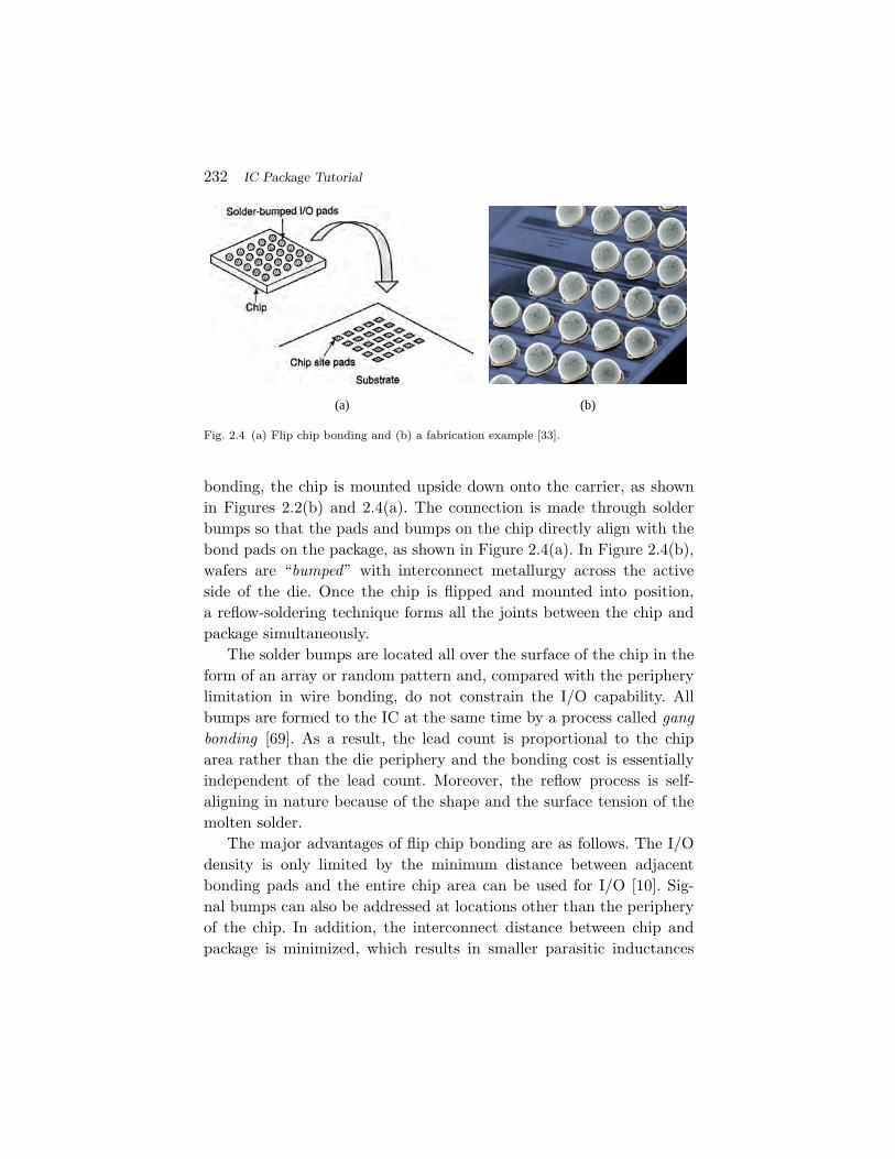
Fig. 2.4 (a) Flip chip bonding and (b) a fabrication example [33].
bonding, the chip is mounted upside down onto the carrier, as shownin Figures 2.2(b) and 2.4(a). The connection is made through solderbumps so that the pads and bumps on the chip directly align with thebond pads on the package, as shown in Figure 2.4(a). In Figure 2.4(b),wafers are “bumped” with interconnect metallurgy across the activeside of the die. Once the chip is flipped and mounted into position,a reflow-soldering technique forms all the joints between the chip andpackage simultaneously.
The solder bumps are located all over the surface of the chip in theform of an array or random pattern and, compared with the peripherylimitation in wire bonding, do not constrain the I/O capability. Allbumps are formed to the IC at the same time by a process called gangbonding [69]. As a result, the lead count is proportional to the chiparea rather than the die periphery and the bonding cost is essentiallyindependent of the lead count. Moreover, the reflow process is self-aligning in nature because of the shape and the surface tension of themolten solder.
The major advantages of flip chip bonding are as follows. The I/Odensity is only limited by the minimum distance between adjacentbonding pads and the entire chip area can be used for I/O [10]. Sig-nal bumps can also be addressed at locations other than the peripheryof the chip. In addition, the interconnect distance between chip andpackage is minimized, which results in smaller parasitic inductances

2.2 Die-to-package Interconnect 233
and resistances that improve signal integrity as compared with wirebond. The power and ground can also be distributed on the packagerather than the chip and can be accessed anywhere on the chip. Onthe other hand, reliability concerns are the major manufacturing dis-advantages of flip chip bonding [33], especially for larger dies or dieswith low K dielectrics. Most flip chip interconnects require underfill tomeet reliability requirements. Non-conductive underfill is used to fill thespace between the chip and the package and mechanically adhere theentire chip surface to the substrate. The system depends on underfillto ensure the intimate attachment of hundreds or thousands of inter-connects between dissimilar materials with vastly different coefficientsof thermal expansion (CTE) and underfill typically precludes assemblyrework after test [33].
2.2.3 Tape-Automated Bonding
TAB technology is the process of mounting a die on a flexible tape madeof polymer material [10], such as polymide, as shown in Figure 2.2(c).The mounting is done such that the bonds of the die, usually in theform of bumps or balls made of gold or solder, are connected to metalstripes on the tape, which allows the die to connect to the package ordirectly to external circuits [10]. The TAB bonds connecting the dieand the tape are known as inner lead bonds (ILB), whereas those thatconnect the tape to the package or to external circuits are known asouter lead bonds, as shown in Figure 2.5.
For ILB, the attachment to the tape is affected by thermo-compression bonding and all bonds to the IC are formed via the gangbonding process. Copper, a commonly-used metal in tapes, can beelectro-deposited onto the tape or simply attached to the tape usingadhesives [10]. The metal patterns of the circuit are imaged onto thetape by photo-lithography. Sometimes the tape on which the die isbonded already contains the actual application circuit of the die [89],and the IC can be tested and burned-in, allowing the elimination ofdefective chips from further packaging process.
The main advantage of TAB, which is similar to flip chip bonding,is its large number of I/O that can be supported by attaching the TAB

234 IC Package Tutorial
(a) (b)
Fig. 2.5 (a) Inner lead bonds and (b) outer lead bonds [89].
tape to the entire surface of the chip rather than just the periphery.Moreover, the shape of the interconnect and the use of copper in tapesprovide low-inductance and low-resistance interconnection, which min-imizes signal distortion [10]. However, TAB requires the use of complexmetallurgy, multi-layer solder bumps in order to affect a bond on eitherthe tape or IC. A TAB tape can only be used for a chip and package,which matches its interconnection pattern. As a result, each TAB tapeneeds to be custom-designed.
2.3 Package Substrate
2.3.1 Lead Frames
The lead frame is made of copper alloy and plated with gold and sil-ver or palladium, either completely or in selected areas over nickel ornickel/cobalt. The silicon chip is usually attached to the lead frame withan organic conductive formulation of epoxy [10]. Gold or aluminumwires are bonded to the aluminum bonding pads on the chips and tothe fingers of the lead frame, as shown in Figure 2.6. The peripheralleads of the package are then attached to the board.
The main advantage of using a lead frame is its ubiquitous assemblymanufacturing capability available worldwide [10]. However, it suffersfrom thermal, electrical, and mechanical performance limitations aswell as lead count restrictions. Typical examples of lead frame sub-strates are quad flat package (QFP) and DIP.

2.3 Package Substrate 235
Standard Cu Lead Frame
Plastic Mold Compound
Bonding Wire
Fig. 2.6 Illustration of lead-frame-based plastic package [10].
(a) (b)
Fig. 2.7 Examples of flex substrate [33].
2.3.2 Flex
Flex is typically a single-sided-polyimide-based circuit tape, althoughtwo-metal tape is available. Either copper is electro-deposited to thetape or rolled copper is attached to the tape using an adhesive. The cir-cuitry is then imaged using a photo-lithography process. Some examplesof the flex substrate are shown in Figure 2.7. The principal advantageof the flex substrate is the tight pitch of the circuit, which can providehigh wiring density suitable for high pin count devices. Moreover, flexsubstrates can be bent or twisted and this ability to conform is requiredfor some 3D applications [33].
The main disadvantage, however, is that the flex must be rigidifiedfor most mainstream IC package applications and there are a limitednumber of metal layers in conventional flex.
2.3.3 Printed Circuit Board
The fine-pitch PCB is a thin core substrate with minimal fiberglass rein-forcement and can be compatible with CO2 laser drilling [33]. It also

236 IC Package Tutorial
provides very fine-pitch plated-through-holes (PTH) and usually con-tains 2 or 4 metal wiring layers. Most importantly, the PCB substratehas a very competitive cost and further cost reductions are expectedin the future as drilling, handling, and testing of thin core substratesare refined. PCB substrate is typically used with a wire-bonding, over-molding, BGA attachment and can also be used with a low-power,low-lead count flip chip interconnect and underfill [33].
The main advantage of this substrate is its competitive cost andcompatibility with both flip chip and wire bonding interconnect. Thedisadvantage is, however, that the PCB substrate has limitations onwireability for high lead count devices and limitations on thermal dis-sipation in cavity up configurations [33].
Figure 2.8 shows the two different configurations for wire bond sub-strates: cavity up and cavity down. Traditional cavity up substrate doesnot allow for good thermal dissipation due to high thermal resistance.Devices are limited to 2 − 3W , depending on die temperature toler-ances. Cavity down substrate construction was invented to address thislimitation and greatly enhances thermal dissipation capability by usinga metallic lid as heat spreader, as shown in Figure 2.8(b). Moreover,cavity down substrates can also facilitate multi-tier wire bonding forhigh lead counts and provides better signal fidelity [33]. A typical exam-ple of a cavity down wire bond is a graphics processor. Note that forcavity down substrates, while power dissipation is excellent, power dis-tribution is still marginal due to peripheral wire bonding [33].
2.3.4 Organic Build-up Substrates
Organic build-up package substrates were developed in responseto the need for high-speed, large-scale integrated chips. Sequential
PCBHeat Heat
PCB
(b)(a)
Fig. 2.8 (a) Cavity up and (b) Cavity down wire bond substrate [33].

2.3 Package Substrate 237
Fig. 2.9 Manufacturing process for multi-layer organic build-up substrate [88].
high-density layers with fine-pitch wiring and laser etched vias inunfilled dielectrics were built around a 2 or 4 metal layer drilled PCBcore, as shown in Figure 2.9 [88]. Note that all signals must flow fromthe top side (chip attach) to the bottom side (balls) through the PTHin the core. As circuits are formed on pure copper conductors, resistanceis low. Additionally, as an insulation layer is formed by organic resin,permittivity is low and the substrate is very lightweight. Furthermore,it has very fine-pitch wiring capability on a per-layer basis.
Lamination in the organic build-up substrates, however, must bebalanced or it is subject to significant warpage. High-density wiringlayers on the bottom side of the package substrates are usually notfully utilized in the design [33]. Also, as mentioned, all signals musttraverse the PTHs in the core, which can represent a large impedancemismatch. Finally, organic substrates are sensitive to moisture whichcan impact the performance of the underfill.
2.3.5 Ceramic Substrates
A ceramic substrate is fabricated with screened metal paste on punchedceramic dielectric sheets that are aligned and fired [33], as shown inFigure 2.10. Ceramic provides a rigid, stable surface with superb dielec-tric strength and very good high-frequency performance. Moreover,ceramic substrate has both a low CTE when compared with organic

238 IC Package Tutorial
Fig. 2.10 Cross-section of ceramic substrate [33].
substrates anda lower thermo-mechanical stresswith largedie [33]. It alsohas higher substrate thermal conductivity, which results in better intrin-sic thermal performance and an insensitivity to moisture. Ceramic sub-strate, however, at the same time creates CTE mismatches with board forlargeBGAmodules because of its lowCTEproperty [33].Taking into con-sideration the limited supply base, a higher infrastructure cost is also oneof the major disadvantages for ceramic substrates [33].
Ceramic substrates have advantages that include low-incrementalcost-per-wiring-layer, a stable dielectric constant, and a low dissipa-tion, which is an important factor for analog and RF designs [33].Additional wiring layers can also be added easily to the design. Onthe other hand, ceramic substrates have a lower wiring density on aper-layer basis compared with organic build-up substrates and maycreate a special problem in flip chip fanout wiring on large lead countdevices. Furthermore, screened and fired metal is not as conductive asplated metal on organic substrates, which causes inferior lateral powerdistribution within the module. However, there are ceramic packagesusing copper instead of the less conductive tungsten.
2.4 Package-to-board Interconnect
The package-to-board interconnect refers to the electrical connectionof an IC to a circuit board, such as the conventional Printed Wiring

2.4 Package-to-board Interconnect 239
Board (PWB). According to the mounting method, the packages cangenerally be divided into three categories: through-hole mounting, sur-face mounting, and direct die mounting. Further categorization can beachieved according to available I/O locations, I/O density, and differentsubstrate types.
2.4.1 Through-hole Mounting
Through-the-board mounting technology has been the traditional low-cost packaging choice and is still used nowadays. The PC board ismanufactured by stacked layers of thin copper sheets and epoxy fiber-glass insulating layers on top of each other [5]. These copper sheetsare patterned and etched to form the interconnection and holes aredrilled through the board and plated with copper. This copper-platedholes serve as the connections between different layers and also con-nect with the packages with their through-the-hole metal pins. Wavesoldering is used to adhere the metal pins with the plated holes andtheir surrounding contact area.
2.4.1.1 Dual-in-line Package
The DIP, as shown in Figure 2.11(a), is one of the earliest packag-ing styles introduced. It is available in low-cost plastic and hermeticceramic types, with through-hole mounting I/O terminals. DIP was
(b)(a)
Fig. 2.11 (a) Dual-in-line package and (b) Single-in-line package [5].

240 IC Package Tutorial
extremely popular in the early era of ICs because it was cost-effectiveand reliably satisfied the electrical and mechanical requirements formany years [5, 69]. With its 8 through 40 I/O terminals, it satisfiedthe needs of a wide range of IC devices and also the assembly require-ments on PCBs either through manual soldering or using automatictermination techniques.
Similarly, single-in-line packages, as shown in Figure 2.11(b), arerectangular with leads on one of the long sides. This type of packagingis mainly used to provide a means for packaging memory chips in ahigh-density format [5]. When inserted into a PCB, many of these canbe placed side by side and stacked closely together, separated by justthe thickness of the package, because the leads or contacts are locatedalong just one side of the package [5].
2.4.1.2 Pin Grid Array
PGA is an array package available with ceramic and organic sub-strates [5]. The pins are arranged across the bottom of the packageand used for through-hole mounting, as shown in Figure 2.12. Theceramic PGA package body is typically constructed as a cofired multi-layered ceramic and wire bonding is usually used for chip to packageinterconnect, although TAB and C4 interconnects can also be used [5].PGA packages played a dominant role in high-density packaging formany years because of their universal assembly compatibility and easyimplementation as a Pb-free interconnect. However, PGA packages haddrawbacks such as high cost, through-holes on the PCB for mounting,as well as the high inductance and resistance associated with pins and
Fig. 2.12 Pin grid array [5].

2.4 Package-to-board Interconnect 241
socket housing [5]. The expensive pins of PGA packages were replacedby cheaper solder balls in BGA packages, as discussed later.
2.4.2 Surface Mounting
In surface mounting, a chip carrier is soldered to the pads on the surfaceof a board without requiring any through-holes [5]. The smaller com-ponent sizes, lack of through-holes, and possibility of mounting chipson both sides of the PC board improve the board density. In addition,the manufacturing process is easier since placing chips is much simplerthan putting pins through-holes.
Surface mounting, however, has disadvantages including thermalexpansion mismatches due to lack of support pins. It is also difficultto test for faulty mounting connection due to electrical and mechanicaldefects.
2.4.2.1 Small Outline Package
A small package body characterizes the small outline peripheral leadedpackages [69]. These packages have surface mount leads on two sides.The primary advantages of a small outline package are its small sizeand its suitability for surface mounting. The gull wing package, shownin Figure 2.13(a), is commonly known as SOP. The SOP is a plasticmolded lead-frame-based package [69]. The lead is formed away fromthe body in the shape of a gull wing, for surface mounting. On the
(b)(a)
Fig. 2.13 Small outline package with (a) gull wing leads and (b) J-bend leads [5].

242 IC Package Tutorial
other hand, Figure 2.13(b) shows the J-bend SOP. It is also a lead-frame-based package with a molded plastic body. The J in the packagename refers to the lead configuration. The leads extend out from theside of the package and wrap underneath the body, forming the shapeof the letter J [69].
2.4.2.2 Quad Flat Package
The QFP is a surface mounting package characterized by a larger bodyand higher lead counts than an SOP package, with soldered leads onall four sides (Figure 2.14) [5]. The QFP is compatible with lead framesubstrates and popular because of its low cost and low power property.It has very high manufacturing volumes and standardized assemblycan be done anywhere in the world at a very low cost. However, thelead counts are still limited by the peripheral and the QFP needs non-standard thermal enhancements for higher power devices, which can beexpensive.
2.4.2.3 Ball Grid Array
BGA has an area array of solder balls and, as a result, can support highlead count devices (Figure 2.15) [33]. Unlike PGA that also has area
(b)(a)
Fig. 2.14 Quad flat package [5].

2.4 Package-to-board Interconnect 243
(b)(a)
Fig. 2.15 Ball grid array [5].
array contact, BGA is compatible with the surface mounting technol-ogy (SMT) board assembly. The package-to-board connection is donedirectly through the reflow process [33]. Moreover, the SMT attach-ment improves board-level wireability with improved power and signaldistribution on the board. Compared with the QFP that also supportsthe SMT, the most evident advantage is the package area: BGAs typi-cally are 20–25% smaller than QFPs, given the same lead count [5]. Inaddition to the mechanical considerations, BGA packages offer betterthermal and electrical characteristics than QFPs [69]. The most obvi-ous drawback to using a BGA package is its significant higher cost.Similar to other SMT packages, BGA suffers from thermo-mechanicalstress on the joints due to warpage and CTE expansion of dissimilarmaterials. Also, BGA interconnects cannot be reliably socketed due tosolder creep.
2.4.3 Direct Die Mounting
Direct die mounting, also known as chip on board, eliminates the chipcarrier and places die directly on a PWB. The die can be attached tothe substrate using wire bonding, TAB, or flip chips with solder bumpconnections.

244 IC Package Tutorial
2.5 Multi-chip Modules and SiP
SiP and MCM in recent years have seen expanded applications [46].MCM interconnect and package more than one bare IC chip (die),enable the designer to drastically reduce the interchip distance (delay),and lead to significant size reduction of the product [10]. On the otherhand, the SiP consists of not only multiple dies, but also passive com-ponents and discrete devices designed and assembled into a standard orcustom package to achieve a modular function previously only accom-plished by using several separated single chip packages [46]. The SiPforms a functional block, or module, that can be used for board-levelmanufacturing.
The traditional two-dimensional (2D) MCMs are divided broadlyinto three types depending upon the substrate dielectric construc-tion, as shown in Figure 2.16 [10]. MCM-L technology uses laminateddielectric-like PWB substrates. MCM-C technology uses ceramic dielec-tric material and MCM-D technology uses deposited dielectric material.
MCM-L packaging is constructed with PCB laminates and the inter-connections on the laminate are almost always copper, and created byphoto imaging [10]. Vias are created through drilling and electrolessplating followed by electroplating. On the other hand, MCM-Cs areconstructed on cofired ceramic or glass-ceramic substrates using thickfilm technologies to form the conductor patterns with fireable met-als [10]. Vias are formed during the conductor screen printing operationand are of the same material as the conductors. MCM-D packagingis based on depositing a dielectric over a substrate, which is usuallyceramic, silicon, copper, other metals, or metal composites [10]. Thedielectrics used can be broadly classified into two categories: polymeric
(b)(a) (c)
Fig. 2.16 (a) MCM-L, (b) MCM-C, and (c) MCM-D [10].

2.5 Multi-chip Modules and SiP 245
(b)(a)
Fig. 2.17 (a) System in package example and (b) 3D stacking [5].
and inorganic. Aluminum, copper, and gold are used for conductor met-allization. Copper and nickel are the most common via fill materials.
The SiP performs all or most of the functions of an electronic sys-tem, and is typically used inside a mobile phone, digital music player,etc. [10]. Dies containing ICs may be stacked vertically on a substrate,as shown in Figure 2.17. This kind of 3D package or Chip Stack MCMcontains two or more chips stacked vertically and takes IC industrya step forward in the Moore curve. Chips are internally connectedby fine bonding wires or solder bumps and usually require an extra“interposer” layer between chips. As shown in Figure 2.17(b), the 3Dstacking technique has been rapidly adopted because 3D stacking inte-gration provides more functionality in less space and it is easier tointegrate die from multiple suppliers through 3D stacking [10].
TSVs can be used to replace edge wiring by creating vertical con-nections through the body of silicon chip in some new 3D packages.With the introduction of TSV, a 3D package is slowly becoming a 3DIC technology in an attempt to increase the number of feasible inter-connects and enhance electrical performance.
SiP or 3D IC simplifies product system board design and assem-bly and provides increased functionality per unit area/volume [10] byheterogeneous integration of materials, devices, and signals. Owingto reduced interchip distance, system electrical performance improveswhile manufacturing costs decrease and at the same time have betterreliability. However, there are a few challenges restraining the indus-try from large volume of commercializing 3D ICs. For example, whentwo dies are 3D stacked for lower RC delay, these two high power

246 IC Package Tutorial
density regions reside on top of each other dramatically increasingpower density of the entire stack. And some 3D IC technologies, such asTSV, are not evolved to be cost-efficient and bring up numerous man-ufacturing yield challenges, such as chip alignment, accurate-controlledbonding, and mechanical stress issues.

3System-in-Package Design Exploration
3.1 Introduction
For high-speed nanometer designs, it is imperative to design the chipand package in a concurrent fashion to successfully meet the design andmarket constraints. The nature and speed of these designs make the tra-ditional separated package-chip design a non-feasible design paradigm.For these designs, the package plays a critical role in meeting the tightperformance and reliability constraints as well as the cost and time-to-market constraints. The tight performance constraints coupled withthe tight time-to-market constraints necessitate a holistic approach tothe design of the components that make up the SiP. For successfuldesign and implementation of the system, characterization and opti-mization of the entire system are needed in order to understand itselectrical, thermal, and mechanical behavior. When the number of I/Osin designs was relatively small (few hundreds) and switching at lowto medium frequencies along with core devices switching at a modestspeed (hundreds of MHZ), package design was a task left till the endof the design cycle when the die is completely designed and taped out.In that paradigm, the design of the die dominated the design cycle
247

248 System-in-Package Design Exploration
and the on-chip constraints in terms of timing, power, and reliabilitywere given the highest priority without regards to the performance ofthe package nor its impact on the performance of the die. Standardpackages in terms of the number of layers and number of pins arecommonly used for designs that do not push the envelop in terms ofperformance constraints. However, as eluded to earlier, these standardpackages would not fit the designs that have a large number of I/Osor that push the envelop in terms of performance and reliabiliy. Forsuch designs, custom packages are designed and optimized as an inte-gral part of the overall design cycle of the system in order to achievea first-pass success. These are the applications that require SiPs andrequire a change in the design paradigm.
Furthermore, a great interest in SiPs stems from the need to extendMoore’s law and continue the aggressive design integration trend.In addition to satisfying the performance and cost constraints of high-end designs, SiPs also provide a medium to integrate multiple tech-nologies and different process nodes in order to realize an efficient,cost-effective, and reliable hybrid system. The integrated componentscould be a combination of digital, RF, MEMS, passive elements, andoptical modules. To be able to analyze the different tiers (layers) ofthis hybrid system, electrical, mechanical, and thermal modelings ofthe various components are necessary.
Design exploration for SiPs tries to balance the needs and con-straints of the various components that make up the SiP as wellas the packaging technology that supports the various components.In addition to meeting the performance, power, and reliability con-straints for all the components that make up the system, it is equivalen-taly important to choose a packaging substrate that satisfies the designconstraints while still minimizing the overall cost and complexity of thedesign cycle.
There are a number of design parameters that need to be exploredand optimized during the package exploration phase. The system designspecifies budgets for performance, power, and reliability that the over-all system must satisfy. Satisfying these system constraints in turn pro-duces a set of constraints that need to be met if the system goals andconstraints are to be met.
3.2 Overview 249
For high-end applications, the cost of the package exceeds the man-ufacturing cost. Thus, during package exploration in general, and forhigh-volume designs in particular, it is very important to choose a pack-age that supports the design constraints while minimizing the totalcost. This can be attained by optimizing the number of layers that apackage has as well as optimizing the design rules and the materialsused to meet the design targets.
3.2 Overview
SiPs serve as a design solution that bridges the continuously wideninggap between the I/O needs of the silicon and support provided by thepackaging technology. There are many design metrics and constraintsthat dictate the selection of a packaging technology. For high-end appli-cations, the package plays a major role in attaining the performanceand reliability goals of the design. These goals constrain the selection ofthe packaging technology in terms of the number, material, thickness ofthe routing and the plane layers in the package. In addition, the size ofthe package is constrained by the size of the design components and thenumber of I/O pins that need to be fanned-out and shielded to attainhigh performance and reduce switching noise. In addition, the heat fluxconstraints as well as the performance and reliability constraints drivethe push for new technologies and higher level of integration such asthose provided by 3D ICs, TSV, and nanotechnologies to circumventthe deficiencies in the cooling technologies and the density gap betweensilicon and packaging. Today, the technology allows us to integrate moretransistors on a single die than we can use and power on. This is due tothe thermal constraints associated with powering such a large numberof transistors (109 s). SiPs alleviate some of these issues by distributingthe components on different dies and allow for a more efficient heatflow. SiPs provide many benefits including:
• Higher level of integration by placing a number of chips alongwith discrete components on a single packaging substrate.
• Higher performance, better reliability, and reduction in time-to-market as compared with the on-chip silicon integration.

250 System-in-Package Design Exploration
• Integration of different interconnection styles such as flipchip, SMT, and other technologies on one substrate.
• Integration of different process technologies and the ability tomigrate to new process technologies of selected componentswithout redesigning the entire SiP.
In this section, we will highlight the design process as well as the designfactors associated with SiPs. These design goals and constraints needto be addressed in order to realize a cost-effective system, which meetsthe performance and reliability constraints. We start by highlightingthe design process and decisions that come with it, and then we discusshow to tackle the problems associated with the chip-package co-designearly in the SiP design cycle. In particular, we will focus the discussionon the two most important design problems that need to be addressed:the design of the channel (signal interfaces) and the design of thepower delivery network. In this section, the emphasis is on the designexploration of SiPs using efficient and reasonably accurate models. Theobjective is to concurrently design the chip(s) and package to meet thedesign constraints in a fast time-to-market fashion. The emphasis hereis on reasonably-accurate models to assess whether the technology anddesign choices that have been made in the design exploration stage aresufficient. At this stage in the design exploration, neither the packagehas been implemented nor the design or floorplanning of the associatedsilicon components is necessarily done. Thus, it is wise neither from aperformance point of view nor from a design-effort point of view to usedetailed analysis models and incur costly design efforts for a virtualsystem that is under design. In a later section, detailed analysis andsimulation methods and algorithms are described that are needed toanalyze the implementation of the chip-package system.
Also, we will address the constraints associated with the physicaldesign and implementation of SiPs and their impact on technologyselection and exploration. In particular, we will discuss the issuesrelated to timing, noise, cooling that are associated with the floor-planning, placement, and routing of the dies and the I/Os. All theseconstraints impact the package technology selection and the designexploration of the overall system. It is necessary to employ a design

3.2 Overview 251
System Specification
Initial Package Synthesis
SiP Prototype: Dies and Package
SoC Pkg
Performance Estimation
Cost Analysis
Mem
Implementation:Interconnection and Technology Mapping
Die(s) Design Package DesignSubstrate Material Specs Cell Design Library Spice/IBIS Models
Tape out
RF
Fig. 3.1 A coherent SiP design methodology.
methodology that addresses all these constraints simultaneously inorder to successfully implement the design and meet its constraints.
Figure 3.1 shows the system design flow of SiPs. The design processstarts with a system specification that outlines the design objectives ofpower, performance, noise tolerance amongst others. In addition, thesystem design provides specifications of the design interfaces needed forthe SiP to communicate with the other modules in the system. Armedwith the system specification, the chip and package designers work intandem to meet the design objectives in a cost-efficient manner. Thechip-package designers build and employ efficient models to study thecharacteristics of the package as given by the substrate material spec-ifications and the given I/O buffers library and models (IBIS/Spice).If the models are in the ballpark of the design objectives, a prototype ofthe chip(s) and package is built. Further refinement and optimizationto the chip design and implementation as well as the package designproceed. A detailed look at the extraction and simulation steps followsto validate the entire system. Although the chip and package design

252 System-in-Package Design Exploration
steps are coupled and some take place concurrently, we expound themhere separately to make the design flow clearer.
From the point of view of the chip, the designer requires the entiresystem and the package in particular, to provide a stable and reliablepower supply, a noise-free (if possible) communication medium, all ina cost-efficient and productive manner.
From the point of view of the package, the designer requires thechips’ I/Os to be planned and routed in a fashion that is amenableto efficient implementation of the package with regards to the numberof package layers needed and the design of the power delivery sys-tem (PDS). The management of the I/O noise in the system dependsgreatly on the type, size, and placement of the I/O buffers. The packagedesigner also desires the package technology to provide a bump pitchthat results in adequate power sources as needed by the SiP withoutdegrading the routability of the package.
In the design exploration stage, decisions on the type of I/O inter-faces as well as the bandwidth needed are driven by the receiving com-ponents and the performance targets for the system as a whole. Themodels needed to concurrently carry out the design and planning of thecore(s), I/Os, and package should be efficient yet accurate to providereasonable metrics in terms of noise, and timing to be able to estimatethe operating frequency range of the interconnect.
3.3 On-chip Design Decisions
During the early stages of SiP planning, the goal of the chip designer isto meet a certain channel bandwidth that is set by the system designspecification. To meet such a bandwidth, the system design specifies thechannel characteristics in terms of characteristic impedance, bit errorrate (BER), timing, timing skew, crosstalk budget among others. Thegoal of the chip I/O designer is to optimize the I/O circuitry and placeand route the I/Os on the chip to the package bumps (redistributionlayer (RDL) routing). To be able to design the channel and meet thesystem-level specifications, the chip designer has to work closely withthe package designer to make sure that any decision taken accounts forthe substrate characteristics.

3.3 On-chip Design Decisions 253
Fig. 3.2 Block diagram of a chip-to-chip communication channel. The main components arethe transmitter, the receiver, and the lossy channel that is composed of the RDL routes,the package traces, and the PCB traces.
3.3.1 I/O Circuit Design
The proper design of the interface channel (Figure 3.2) must adhere toa complex set of specifications and constraints. These include voltagelevels and noise, BER, signal jitter, and slew rate. Proper design andoptimization of these circuits are needed to meet the design specifica-tions at an acceptable cost in terms of area and power [6, 21, 34, 53, 66].
To meet the performance and signal integrity constraints for the I/Odrivers, good models of the package and board are needed to accountfor the capacitive loading and coupling as well as the inductive couplingin the system. Early in the design cycle where the package is not routedyet or where no board models exist, good estimates are needed. In high-end designs, it is no longer sufficient to use ad hoc metrics such as rulesof thumb to make decisions on the type and size of the I/Os as well ason the capacitive and inductive values of the load that the driver sees.Good virtual models that are able to capture the package and boardeffects are needed.
Figure 3.3 shows the modeling components needed to estimate theperformance and noise metrics of the signal interface in SiPs. Guided bythe channel interface spec, the I/O circuits are partitioned into powerdomains, each with a given voltage level. Each of the power domainsneeds to be characterized to study the impact of the package on thechannel bandwidth. Also, the model studies the impact of the noiseinjected by the I/O drivers on the power delivery network and theother drivers on the chip.
To control the power consumption of the I/O buffers, the circuitimpedance should be reduced. However, good design of the circuitshould take into account the impedance of the lossy transmission

254 System-in-Package Design Exploration
Fig. 3.3 Quick simultaneous switching noise estimation model that uses the IBIS modelsof the drivers, the package layer parameters, and the trace model of the signal routes fromthe driver to the package pins.
medium in the package and PCB. The impedance should be as closeas possible to that of the channel or proper termination is needed toreduce any reflections that result from the impedance mismatch. Forhigh-bandwidth SOCs, there is a number of high-speed I/O circuits inuse today that employ different signaling techniques such as LVDS tooptimize the delay, power, and noise [40]. There is a set of standardI/O buffer circuits that are commonly used such as high-speed transferlogic (HSTL), series-stub transfer logic (SSTL), and PECL. Differentialsignaling is also very common to reduce the noise associated with thehigh-switching rate and improve the resultant bandwidth. HSTL andSSTL are two very popular design choices for high-bandwidth appli-cations. For proper functionality of these circuits, tight control on thedriver and receiver’s impedance is needed. For example, SSTL requiresits output impedance to match that of the transmission line impedanceseen in the package along with maintaining low capacitive loading atthe receiver’s end. This results in a critically damped waveform thataids in reducing noise and crosstalk as well as keeping the clock anddata jitter under control [19].
3.3.2 I/O Buffer Physical Planning
There are physical and electrical constraints that need to be met whenplanning and placing the I/O circuits on the die [12, 41, 44, 60, 91].The floorplan of the die imposes physical and timing constraints on the

3.4 Package Design and Exploration 255
I/O circuits. There are timing constraints that need to be honored onthe path from the I/O circuits to the latches connected to them. Thereare timing skew constraints associated with the placement and rout-ing of differential pairs [52, 95]. There are power and signal integrityconstraints that need to be honored, chief amongst those is the simul-taneous switching noise (SSN) constraint [18]. For correct modeling ofthe SSN effect, the entire circuit loop from the I/O output pin to therespective power pin needs to be modeled. This necessitates modelingthe virtual trace routes in the package. It is not acceptable anymore towait until after routing the package to do this analysis and verify thatthe signal and power integrity constraints are met [11, 47].
3.3.3 On-chip Power Design and Planning
One of the primary objectives in the design of a power network isthe delivery of a low-impedance stable power supply level from DCto the transition frequency of the signals. The success of this missionrequires a close interaction between the chip and package. On the chip,a reliable power grid with an acceptable dc voltage drop is of paramountinterest. If the on-chip IR drop is not controlled, the performance ofthe switching devices is directly impacted. The on-chip power networkis affected by on-chip noise sources such as the simultaneous switchingof the on-chip devices as well as perturbations due to capacitive andinductive coupling in the package. To achieve a low-impedance stablePDS for the whole frequency spectrum of interest, the entire powerdelivery network needs to be taken into account. The design shouldaccount for low-, medium-, and high-frequency sources of noise. ThePCB planes and traces are the source of low-frequency noise whilethe package with its planes, traces, and vias play the major part inthe mid-frequency noise injected into the power delivery network. Thehigh-frequency noise is due to switching rates in the chip near to thecircuit.
3.4 Package Design and Exploration
Meeting the performance target of the system at an acceptable priceis the most important criterion for a successful design. If cost is not

256 System-in-Package Design Exploration
accounted for, an overdesigned system in terms of the number of layersin the package and the spacing on each layer will meet the performancetarget. Such a system is not a viable solution due to the exorbitant cost.Owing to the difficulty of taping out high-speed package designs, it islikely that a package solution can be more expensive than the chip.For high-volume designs, such a solution is not acceptable. Early inthe chip-package design stage, not much is known about the switchingprofile of the circuits as well as the size and placement of the I/Obuffers. Therefore, constraints must be defined for co-design. This isthe primary reason making package design difficult.
3.4.1 Package Stack-up Order
Once a package substrate is chosen, one of the most important deci-sions in deciding on a package design is the number of layers (substratebuild-up) and the determination of optimal design rules. Often, when apackage has more than two layers, a core layer (very thick) is designedand a number of layer pairs are added by mirroring the layers aroundthe core layer. For example, for a package that has three layers, thesubstrate build-up would be 111. For a package that has five layers, thesubstrate build-up would have 212, which means a core layer, and twolayers above it and two layers below it. Each additional layer pair addsto the cost of the package. For an efficient package design, the numberof layers should be minimized while meeting the design constraints andperformance targets [22, 61].
3.4.2 Substrate Layer Assignment
The decision of layer assignment is a very crucial one with respect toperformance, reliability, and cost of a package. For high-speed designs,more layers are assigned to power and ground in order to ensure asteady low-impedance power supply as well as reduce the inductiveand capacitive coupling in the package to shield the signal traces andimprove the performance. The need for more power planes increasesthe cost of the package and hence the overall system. On the otherhand, lower speed designs require fewer layers and thus have a lowercost [3, 25, 28, 57, 58].

3.5 Voltage Domain Planning 257
When characterizing the package either through measurements ormodeling, the computed parameters such as SSN or package resonanceimpact the decision of how many package layers to be dedicated forpower and ground.
To study and optimize the variance in high-speed signaling char-acteristics such as Z0 (characteristic impedance), insertion loss, andcrosstalk as functions of key substrate design dimensions, design ofexperiment (DOE) methods are employed by high-end design houses.As for Z0, target center value and tolerance are given by chip andsystem designers. The design rules have to be determined to meet theserequirements. In addition, they have to be optimized for low-cost andhigh-volume manufacturing. The primary constraint is trace width. Anarrower trace results in larger variance in characteristic impednaceand a wider trace inordinately constraints wiring density [26]. Mostoften, the design rules are overdesigned and are provided by the sub-strate manufacturers as templates to be followed by the package designteams.
3.5 Voltage Domain Planning
The different technologies in SiPs are referenced to a number of volt-age domains, each with a voltage level decided by the circuitry in themodule, the process node, or a performance constraint for that tieror component. In addition, each voltage domain is composed of oneor more power domains. These power domains constitute logical parti-tioning of the different signals and buses in the system (Figure 3.4).
3.6 Modeling and Analysis Decisions
For pre-layout characterization of the package, lumped models or trans-mission line models are utilized. Package designers are often familiarwith transmission line models, and there are mature tools that can beemployed to calculate S-parameters to ascertain the package behaviorand the signal characteristics.
Package substrates should be designed to meet the time-domainspecifications as well as frequency-domain specifications such as

258 System-in-Package Design Exploration
insertion loss or crosstalk. Eye opening and jitter define time-domainconstraints that the system must meet. These specifications themselvescannot be guaranteed by characterizing only the package substratebecause the eye diagram is determined by the characteristics of the totalchannel, including PCB and the package, on the other end (Figure 3.5).
Fig. 3.4 This picture shows a solid plane that provides a stable reference for the tracesabove and below it. This design provides a tighter return path loop, which renders theeffective loop inductance smaller.
Fig. 3.5 The picture on the right shows a poor voltage domain partitioning in the package.The perforated plane does not provide a stable reference and causes a large inductance loopand noise problems in the package.

3.7 SiP Design Problems 259
To validate the channel, worst-case time-domain simulations are usu-ally carried out [26, 27].
For systems where building a detailed model of the chip-package atvery high frequencies (millimeter-wave designs), measurements are uti-lized to design and verify systems. Also, for measurement-based model-ing of the system, extracted models can be used to design and optimizesystems. This method is feasible for small systems with a small numberof I/Os. However, for systems with high number of I/Os, measurement-based models will be prohibitively expensive, and more emphasis isplaced on modeling and simulation for the design and optimization ofchip-package systems.
For simulation methodologies, the type of models used becomesa critical one. In general, the more detailed the model, the more itcan capture the intricacies of the system under design. However, suchdetailed models if exist come at a cost in terms of simulation and design.In the early phases of the design where neither the I/Os are placed northe package is routed, detailed models are not warranted.
In order to specify the major factors that affect the critical param-eters of the package design, DOE technique and statistical analysis areused. Both 2D and 3D electromagnetic analyses and circuit model sim-ulations are carried out in design optimization process. Passive charac-terizations are also carried out to get the basic parameters used in thepackage design.
3.7 SiP Design Problems
In this section, we will expound the following two most importantdesign problems that need to be addressed early in the design cycle:
(1) power integrity modeling,(2) timing and signal integrity modeling.
These problems dictate and define the type of I/O circuits needed aswell as how they are placed and routed. Also, these decisions definethe package characteristics in terms of the number of layers, the designrules followed in the package implementation, and the layer assignmentin the package.

260 System-in-Package Design Exploration
3.7.1 Design and Planning of PDS
The design of the PDS requires time- and frequency-domain modelingand analyses of the chip and package. To control the size and complexityof the RLC model of the power network, the modeling and validationof the chip and package power networks are done in isolation. Duringthe design planning stage of the chip and package, RLC models of thevarious I/O power domains along with the package voltage domainscan be built and analyzed. As for the chip power network, the pack-age power network plays more of a prominent role in wire bondingdesigns as opposed to flip chip ones. For flip chip packaging, there isabundance of C4 power bumps feeding the core logic as opposed to thewire-bonded designs where the power is constrained to be delivered bythe power pads on the periphery of the chip. Insertion of decouplingcapacitors (decaps) is an integral part of the power design of SiPs. Agood understanding of the behavioral model of the capacitors and thedynamic power fluctuation is necessary in order to accurately predictthe noise on the voltage rails [83].
3.7.2 Design and Planning of Signal Interface
It is imperative to model the entire channel that signals go through asthey make their way from the transmitting chip side to the receivingside. This channel consists of the on-chip transmitters, the differentsubstrate layers in the SiP including the package layers, and onto thereceiving end. If the transmitter and the receiver are not in the sameSiP, then the PCB traces should be modeled as well as the receiv-ing SiP. These stages could be a number of PCBs and intermediarieswhose electrical characteristics affect the performance and reliability ofthe signal. Modeling the signal transmission into and out of the chiprequires understanding the behavior of the signal transmission in thepackage. Also, in order to study the power needs of the chip, we needto understand the power network in the package, which carries powerfrom the voltage regulator module (VRM) down through PCB and upto the chip. At the early stages of chip planning, many of the importantcomponents of this signal transmission system are not defined.

3.7 SiP Design Problems 261
CompactRLC
Model
Lg
1
2
16
RG
rG
RP
rP
CL
LbpLppRpp Rbp
CppCbp
RL,bpLL,bp
RL,pp LL,pp
CL,bp CL,pp
Fig. 3.6 RLC model for estimating the noise and timing of the signal interface early in theSiP design stage.
3.7.2.1 Signal Interface Characterization
Signal interface characterization in terms of bandwidth, jitter, and skewhas to be carried out before an SiP is taped out. For design and mod-eling of the channel, Figure 3.6 shows a basic model that can be con-structed as soon as the chip and package decisions outlined above havebeen implemented.
Figure 3.6 shows a detailed model for estimating the channel noiseas well as the signal timing, skew, and jitter. The model’s accuracy isreasonable in the design planning stage before the chip is fully imple-mented and the package is routed. The parasitics of the RDL routesand those in the package reflect virtual routes of the signals basedon the power and voltage domain partitioning on the chip and in thepackage. The RLC model of the plane is shown in reduced form, andit does not have to account for any vias at this stage in the design.

262 System-in-Package Design Exploration
The subject of channel design and characterization is treated in moredepth in [6, 21, 34, 53, 66].
It is often the case that both the chip and package share some layersor voltage domains. In such cases, some of the package integrity prob-lems could creep into the chip and vice versa. A simple example of sucha scenario is when both the I/O signals and the on-chip signals sharethe same ground plane. Any ground bounce phenomenon or a generalpower integrity problem could travel in the ground plane and reach theon-chip devices. To remedy such problems, careful analysis and charac-terization of the I/O signals and the power planes in the package mustbe done. In addition, for enhanced reliability of the system, the chipand package should be isolated from each other as much as possible forpower noise.
The following section expands on detailed modeling and analysistechniques for sign-off and validation of the SiP design based on thedecisions outlined above.
3.8 Parasitic Modeling for Design
As technology scales down towards nano-regime and the trend of SiPcontinues, the industry is moving toward higher pin-count, greater com-plexity, higher-density packaging with increased functionality, higheroperating frequency, lower operating voltages, and reduced packagesize. This trend has also brought about the increased less ideal wiresand traces, as shown in Figure 3.7. The non-ideal effects can generallybe categorized into resistive, capacitive, or inductive parasitics, impact-ing the power and signal integrity of die. To capture those non-idealeffects and to characterize the electrical performance of the package,in this section we will discuss how to extract the full parasitics of apackage and form circuit models to facilitate the design for power andsignal integrity.
3.8.1 Definition and Effects of Inductance
Among all the parasitics, it is the inductive effect that makes the extrac-tion and modeling of the package differ from that of the chip. In thissection, we will introduce the concept of inductance.

3.8 Parasitic Modeling for Design 263
Fig. 3.7 Resistive, capacitive, and inductive parasitics of a package [87].
Inductance is the property within an electrical circuit where achange in the current flowing through that circuit induces an elec-tromotive force that opposes the current change. All inductors haveinductance associated with them. The inductance of a loop increasesas the area of a loop is increased. Such a loop can be formed startingfrom the driver, through power and ground lines (both are AC ground),substrate or other signal lines, then returning to the driver. As thereturn current always chooses the paths with the smallest impedanceZ = R + jωL that varies with frequency ω, the inductance is alsofrequency-dependent.
At low frequencies, the resistive part R dominates and accord-ingly, the return current spreads with a relatively large inductance.With the increase of frequency, jωL becomes dominant and the returncurrent concentrates closer to the conductors. Hence, the inductancedecreases and the resistance increases somewhat with the increase offrequency. At very high frequencies, the skin effect becomes importantand the current concentrates to the surface and the resistance increases

264 System-in-Package Design Exploration
proportional to the square-root of the frequency. As an example, thefrequency dependence of both the resistance and the inductance of aninterconnect is shown in Figure 3.8.
It is clear from this that inductance can have significant impacton the power and signal integrity, causing overshoot, undershoot andincreased propagation delay as shown in Figure 3.9. The voltage over-shoot or undershoot can exceed VDD or GND and may threaten the
R(ω)
proximity effectskin effect
L(ω)L(ω)
ω
Fig. 3.8 Frequency dependence of package resistance and inductance.
Fig. 3.9 Overshoot, ring back, and propagation delay caused by inductive effect [2].

3.8 Parasitic Modeling for Design 265
reliability of the circuits, while the increased propagation delay maycause timing violations.
Numerous techniques have been proposed to effectively extractthe parasitic elements of the package, especially the inductive para-sitics. Below we will briefly review three types of methods: the par-tial element equivalent circuit (PEEC) method that derives the modeldirectly from the Maxwell equations, a loop inductance method that isknown for its efficiency and can be used in design iterations, and themeasurement/simulation-based S-parameter methods.
3.8.2 PEEC Models
As a brief review,1 the full-wave PEEC model starts by cutting thepackage into cells, where for each cell the following equation is solved,which is the solution to Maxwell’s equations:
n × �E0(�r, t) = n ×(
�J(�r, t)σ
+∂ �A(�r, t)
∂t+ �Φ(�r, t)
). (3.1)
In the above equation, �E0 is an external electric field, �J is the currentdensity in the conductor, �A is the magnetic vector potential, and Φis the electric scalar potential. The magnetic vector potential �A andscalar potential Φ at �r = (x,y,z) are
�A(�r, t) = µ
∫V ′
G(�r, �r′) �J(�r′, td)dV ′, (3.2)
Φ(�r, t) =1ε
∫S′
G(�r, �r′)ρ(�r′, td)dS′, (3.3)
with td being the retarded time
td = t − |�r − �r′|c
, (3.4)
where c is the speed of light in the medium, ρ is the surface chargedensity, and G is the Green function for homogeneous media:
G(�r, �r′) =14π
1
|�r − �r′|. (3.5)
1 For a complete theoretical derivation of the PEEC models, interested readers are referredto [71].

266 System-in-Package Design Exploration
Substituting the vector (3.2) and scalar potentials (3.3) into (3.1) yieldsthe following integral equation:
n ×(
− �E0(�r, t) +�J(�r, t)
σ+ µ
∫V ′
G(�r, �r′)∂ �J(�r′, t)
∂tdV ′
+�ε
∫S′
G(�r, �r′)ρ(�r′, td)dS ′)
= 0 (3.6)
To solve (3.6), current and charge densities are discretized into vol-ume and surface cells, respectively. Applying the KVL and the Galerkinmethod [29] leads to the full-wave PEEC models and circuit matrices canbe obtained accordingly.
The PEEC model has several advantages: first, without prior knowl-edge of return paths, current loops can be reconstructed by assumingthat current returns at the infinity. Second, it can exactly evaluate theskin-depth effects by discretizing the conductors as a combination ofmany thin-wires (filaments). This model is called the volume filamentmethod.
Recently, a library-based PEEC extraction was presented in [37]and can be used inside iterative design and verification. However, asthe PEEC model includes mutual inductances between every pair ofconductors, the resulting circuit matrix is dense [32]. Accordingly, spar-sification or acceleration methods are required for large models.
The most direct and perhaps the simplest way to sparsify the matrixis by truncation. The idea of truncation is to remove all the couplingterms that are below a user-specified threshold. However, a majorproblem with this approach is that the resulting matrix can becomenon-positive definite. As a result, the sparsified system is no longerpassive. To address the passivity problem, block-diagonal sparsificationhas been proposed. It uses circuit-topology-based partition techniques,which can guarantee the passivity of the sparsified model.
For specific problems of long on-chip wires, alternative approacheshave been proposed. As an alternative, one approach associates eachsegment with a distributed current return path out to a shell of cer-tain radius [49]. The inductive coupling between segments with spacinggreater than the specified radius is neglected. To compensate for the
3.8 Parasitic Modeling for Design 267
truncation, the inductance values of the segments within the radiusare shifted properly. Such a shift-truncate method can guarantee thegeneration of positive definite sparse approximations of the originalmatrix. However, it is not straightforward to determine the value ofthe shell radius. An extension of this work [38] uses a moment-basedalgorithm to compute the shell radius. Another approach for limitingthe inductive interaction is proposed in [72], which introduces return-limited inductances for sparsification and the use of “Halos” to limitthe number of mutual inductances.
Another alternative method is discovered from the fact that theinverse of the partial inductance matrix usually has a higher degreeof locality and sparsity [24], which is very similar to the capacitancematrix. It is very easy to do the truncation and sparsification on theinversion of the partial inductance matrix. However, such a methodrequires inversion of the partial inductance matrix, which is very expen-sive. In addition, a special circuit simulator is required to handle theinversion of the inductance matrix.
Finally, model order reduction for the linear portion of the circuitcan be combined with the gate models and simulated in SPICE [62].The linear circuit can also be parameterized [76] or symbolized [78].The reduced order models have a much reduced size and yet serveas good approximations of the input–output behaviors of the originalcircuits. In turn, they are very efficient in terms of simulation time.One of the problems with the model order reduction techniques is thatthey cannot handle circuits with a large number of ports well.
3.8.3 Loop Inductance Models
Though accurate, the high complexity of not reduced PEEC modelsprohibits them from being used in design iterations. As discussed pre-viously, such complexity comes from the fact that for the simple prob-lem with equal return conductors, the inductance is formed by loopcurrents, and partial mutual inductance exists between all pairs of con-ductors. Instead of using the partial inductance, a simplified approachusing the loop inductance model is commonly used with less accuracybut more efficiency.

268 System-in-Package Design Exploration
For 2D structures, the inductance model [86] is developed in athree-step process: to start with, individual conductor cross-sectionsare sub-divided into sections smaller than the skin depth at the max-imum frequency of interest, as is done for the volume filament modelin PEEC. With this discretization, uniform current density can beassumed in each section. Next, resistance and inductance values arecomputed for each conductor cross-section assuming uniform currentdensity in each cross-section. This allows the well-developed inductanceformulas to be employed for computing the L matrix. Finally, the cou-pled RL skin-effect macromodel depicted in Figure 3.10(a) is analyzedat several points in the frequency domain. Such a method still suffersfrom the complexity problem as the obtained linear equation needs tobe solved at multiple frequency points, and at each point a matrix fac-torization or inversion is required. This method is the foundation offrequency-dependent extraction tools such as FastHenry [43].
To reduce the number of solves required and to reduce the size ofthe circuit synthesized, Kim et al. [45] propose to use smaller num-bers of the π-segments to model the frequency-dependent behavior.Moreover, only the frequency characteristics at maximum frequencyand dc (Rmax,Lmax,Rdc,Ldc) are required to synthesize such a circuit.Accordingly, expensive methods such as [86] only need to be appliedat those two frequency points, and the characteristics at any frequencypoints between can be efficiently obtained by solving the compact modelinstead. However, the efficiency of those two methods are still limited
Fig. 3.10 RL ladder circuit to model frequency dependence.
3.8 Parasitic Modeling for Design 269
because finding Rmax is costly and the synthesis procedure is iterative.Most recently, Krauter and Mehrotra [48] propose the construction of acompact ladder circuit as shown in Figure 3.10(b) without the necessityof calculating Rmax or employing iterative synthesis.
3.8.4 S-parameter Methods
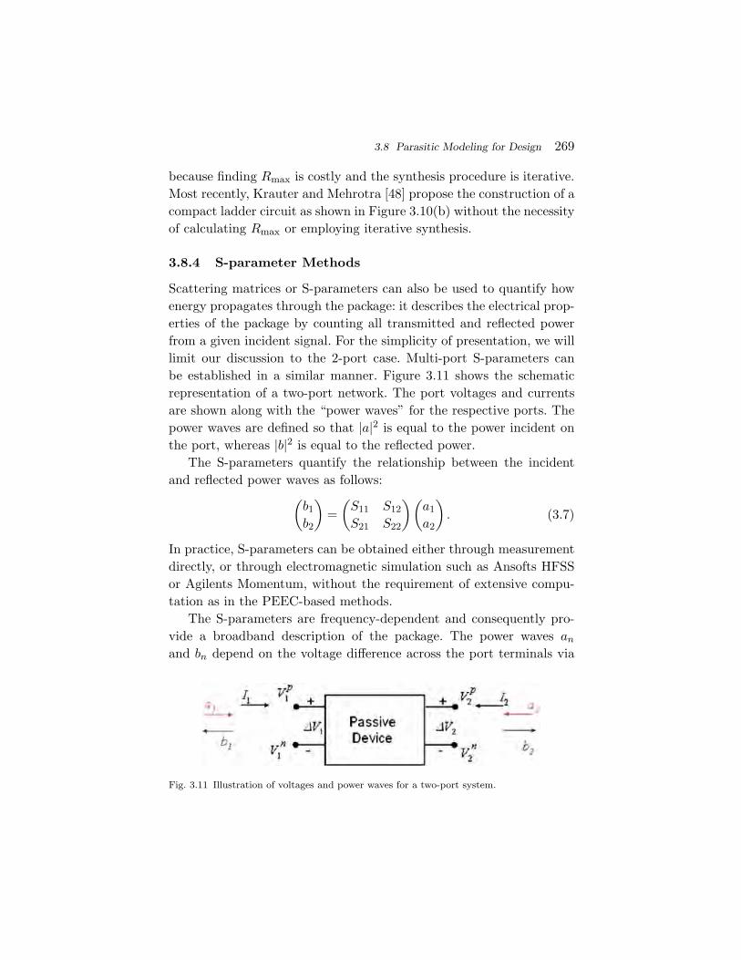
Scattering matrices or S-parameters can also be used to quantify howenergy propagates through the package: it describes the electrical prop-erties of the package by counting all transmitted and reflected powerfrom a given incident signal. For the simplicity of presentation, we willlimit our discussion to the 2-port case. Multi-port S-parameters canbe established in a similar manner. Figure 3.11 shows the schematicrepresentation of a two-port network. The port voltages and currentsare shown along with the “power waves” for the respective ports. Thepower waves are defined so that |a|2 is equal to the power incident onthe port, whereas |b|2 is equal to the reflected power.
The S-parameters quantify the relationship between the incidentand reflected power waves as follows:(
b1
b2
)=(
S11 S12
S21 S22
)(a1
a2
). (3.7)
In practice, S-parameters can be obtained either through measurementdirectly, or through electromagnetic simulation such as Ansofts HFSSor Agilents Momentum, without the requirement of extensive compu-tation as in the PEEC-based methods.
The S-parameters are frequency-dependent and consequently pro-vide a broadband description of the package. The power waves an
and bn depend on the voltage difference across the port terminals via
Fig. 3.11 Illustration of voltages and power waves for a two-port system.

270 System-in-Package Design Exploration
the relationship
∆Vn = (an + bn)√
Zon , (3.8)
In =an − bn√
Zon, n = 1,2, (3.9)
where n is the port number and Zon is the characteristic impedance ofthe port.
In order to use the S-parameters for time-domain simulation, weneed to extract a circuit model from the measured S-parameters. Thisis often a tedious task and it even requires a heuristic guess to con-struct the topology of equivalent circuit, as different topology wouldgive different values of the element for the same S-parameters. Theproblem is even more complicated when we also need to make surethat the extracted circuit is passive and causal. Recently, Lee et al. [54]proposed an efficient way by first converting the S-parameter to theT-parameter (transmission matrix), which can be further representedby a cascaded network of series RL and shunt GC ladder circuit.
3.9 In-package Power Integrity
With the technology scaling down to 45 nm and beyond, power integrityhas become the major bottleneck for the reliability of high-performancesystem in SiP integration. The reduced supply voltage and increasedclock frequency and chip density have made the circuits more vulnera-ble to power supply noise than ever before.
SSN, also referred to in the literature as ∆I noise, is considered tobe the major threat to the power integrity. Accordingly, we will focuson SSN in this paper. It primarily occurs due to a very large amountof instantaneous P/G current from the simultaneous switching gates,which is quite common in clock synchronized circuits. SSN is mainlyan inductive noise and can be generally characterized by the equationVn = L(dI/dt), where Vn is the magnitude of SSN. L is the parasiticinductance of the chip and the package, and I is the total switchingcurrent. In other words, the magnitude of SSN is proportional to thetotal parasitic inductance and to the rate of change of the switchingcurrent. SSN noise causes supply voltage fluctuation; it reduces noise

3.9 In-package Power Integrity 271
Fig. 3.12 Illustration of power delivery system.
margin of digital circuits; it shifts the operating point of analog circuits,it decreases the effective driving strength of the gates; and it causesoutput signal distortion (e.g., jitters) impairing signal integrity.
Figure 3.12 illustrates a lumped model for PDS for board, package,and chip, where L0, Lb, and Lp are the inductance of power regulator,board, and package, respectively. Cb, Cp, and Cc are the capacitanceof the board, package, and chip, respectively, Vdd is the power supplyvoltage, and I(t) is the on-chip switching current. A set of their typicalvalues is also provided [75].
Such a PDS structure leads to three distinct impedance peaks, iflooking from the chip into the PDS, as shown in Figure 3.13 [7]. The firstand smallest peak is in the kHz range, mainly caused by the couplingbetween the power regulator and the board. The second in the MHzrange, mainly caused by the coupling between the package and theboard. The third in the 100 MHz range, mainly caused by the couplingbetween the chip and the package. As discussed in the previous section,the SSN from I/O buffers is first injected into PDS via such coupling.
SSN is most significantly observed around the output pads of thechip. The main reasons are in three folds: First, in order to drive largeoff-chip loads, the I/O buffers are usually very large in size, drawing sig-nificant amount of instantaneous currents when they switch to changethe output binary value, as shown in Figure 3.14. Second, in clock syn-chronized chips multiple I/O buffers tend to switch simultaneously tocreate a large surge current with a sharp slope. Third, the parasiticinductance of the power distribution network of the package, including

272 System-in-Package Design Exploration
Fig. 3.13 PDS impedance seen from the chip [7].
Fig. 3.14 SSN caused by the simultaneous switching of I/O buffers.
the interconnections to both the chip and the board, is usually in therange of a few hundred pico-Henries. Such large inductance has madepackage a major contributor to the SSN.
In order to reduce SSN, many design techniques have been proposedin literature. They target at various design freedoms in different designstages, trying to reduce the parasitic inductance, or trying to reducethe impedance between the power and ground plane. In this section, wewill briefly discuss a few of these techniques and point out the criticalissues in each of them. A more thorough review of these techniques canbe found in [77].

3.9 In-package Power Integrity 273
3.9.1 I/O Planning and Placement
I/O placement plays a key role as the interface between chip and pack-age designs in a co-design flow. Most of today’s high performance ICsare designed with flip chip technology, which eliminates wires for chip-package bonding. The bonding is achieved through bumps via the SMT.As discussed previously, I/O cells are first connected to bumps on thedie via RDL routing, then the die is “flipped” and mounted on thesurface of the substrate, where bumps are connected to bump pads onthe substrate. Finally, package trace routing is performed to furnishthe connection between bump pads to package pins.
For flip chip designs, there are two types of I/O cell placementschemes: peripheral I/O and area I/O. Peripheral I/O scheme restrictsthe placement of I/O cells at the chip boundaries, and it is a cost-effective way to transform traditional wire bonding chip designs to flipchip designs. Area I/O scheme allows I/O cells to be placed anywherewithin the die area and it is inherently suitable for flip chip packaging.In [23], the peripheral and area I/O schemes are also called extrinsic andintrinsic flip chip designs, respectively. Interested readers are referredto [90] for more details.
For I/O planning and placement, we need to assign the pins andpads to different signals and P/G supply. Different assignments cansignificantly impact the system performance, including the signal andpower integrity.
While so many factors can affect the I/O placement, in this sec-tion we will focus on the issues that need to be considered for SSNsuppression. There are mainly two criteria.
First, as illustrated in Figure 3.15, the power and ground pins andpads for analog and digital circuits should be separated whenever pos-sible. As such, the switching noise generated by the digital portion ofthe system will not affect the operation of the analog portion of thesystems, which is generally more sensitive to power supply noise.
Second, the pads and pins for power and ground should be madeas many as possible. With the increased P/G pin/pad number, theinductance will become smaller (parallel connection) which leads tolower SSN. In addition, the slew of the relationship between SSN and

274 System-in-Package Design Exploration
Fig. 3.15 Separation of digital and analog power/ground pads.
0 20 40 60 80 1000
0.05
0.1
0.15
0.2
0.25
0.3
0.35
Number of switching I/O buffers
max
imum
SS
N (
V)
4 P/G pin/pads
8 P/G pin/pads
16 P/G pin/pads
32 P/G pin/pads
64 P/G pin/pads
Fig. 3.16 Relationship between SSN and the number of switching I/O buffers for differentnumbers of power/ground pins/pads.
the number of switching I/O buffers becomes smaller with the increasein power and ground pin/pad number, as shown in Figure 3.16.
The robustness of the power delivery in package mainly dependson the resistance, inductance, and capacitance of the delivery pathand the mutual inductance and coupling capacitance formed betweenthe path and any other surrounding metals including traces and P/Gplanes. With the low inductance (pico-Henries) and the large capaci-tance (micro-Farads), metal planes provide much lower impedance for

3.9 In-package Power Integrity 275
return current paths than traces or point-to-point wires. Accordingly,the plane structures are much more superior in delivering power thanother traces.
Accordingly, the layer stackup and assignment problem can be for-mulated to assign signal nets and P/G planes to different layers in thepackage so as to minimize the number of layers required while maintain-ing power integrity. At this point, we will look from the power integritypoint of view, and during this process the following guidelines shouldbe followed [4]:
(1) Solid reference planes must be parallel to the routed signals.(2) Consider return current amplitude when determining power
plane thickness.(3) Pair up power and ground layers to provide additional “free”
capacitance, reducing power supply noise.(4) Use extra ground planes instead of power planes to isolate
sets of routing layers.(5) Use many vias to connect multiple ground layers.(6) Minimize plane splits. Split planes create return path dis-
continuity and cause additional crosstalk problems. Whensignals travel over the split, this causes additional forwardand reverse crosstalk. Vias can also create the same effect asa split plane because the reference plane may change.
3.9.2 Decoupling Capacitance Insertion
Decaps, which act as charge storage devices and low pass filters for acsignals, serve as another technique to enhance the power integrity byreducing voltage fluctuation in the PDS. An illustration of the decapinsertion in a multi-layer package is shown in Figure 3.17.
For package decoupling purposes, discrete decaps ranging from a fewpico-Farads to sub-micro-Farads are used. These decaps are not per-fect and their frequency responses can be modeled with an equivalentseries capacitance (ESC), an equivalent series inductance (ESL), andan equivalent series resistance (ESR), with different effective ranges.Generally, for the same amount of ESC, a decap with a lower ESLis more expensive [99]. The expensive decaps may not always be the

276 System-in-Package Design Exploration
Fig. 3.17 Resistive, capacitive, and inductive parasitics of a package [17].
best choice for electrical performance. Moreover, the effectiveness ofthe decaps depends on its connected electrical environment and there-fore varies with locations. Low-impedance decaps can be put at pre-defined locations in the package. Therefore, the sizes and locations ofthe decaps need to be optimized for the most effective design with theminimal cost.
In the literature, there exist two different types of metrics used toevaluate the SSN: the frequency domain impedance metric and thetime-domain noise metric. As a frequency domain impedance metric,the impedance at given ports is required to be lower than a computedtarget impedance in the entire frequency bandwidth of interest. Accord-ing to Smith et al. [80], the target impedance can be computed asfollows:
Zt =δVdd
I, (3.10)
where δVdd is tolerable variation of Vdd and I is the switching current atthe given ports. In [99], Zheng et al. also proposed a weighted combinedimpedance to consider the coupling between ports. Despite its ease ofcomputation, the impedance metric may lead to significant overdesignas the impedance is a pessimistic estimation of the noise rather than adirect proportion to the noise [15]. Physically, the metric assumes thatall the frequency components have the same impedance with the samephase and add up to the total noise. In fact, the current is not uni-formly distributed in the entire frequency band, and impedance can be

3.9 In-package Power Integrity 277
different at different frequencies. Also, different frequency componentshave different amplitude and phase and may cancel each other. Theimpedance also varies with the frequency and does not need to be verysmall in the entire frequency band.
As an improvement over the frequency domain impedance metric,a time-domain noise metric can be used. Chen and He [15] propose touse the maximum voltage drop at all ports of interest as the metricto evaluate the SSN. Shi et al. [79], Yu et al. [96], and several othersintegrate the time-domain waveform over the time interval where thevoltage drops below the tolerance bound, as shown in Figure 3.18, andtake the sum over all the ports as a metric. Such a metric is moreaccurate in the sense that it also takes the time duration of the noiseviolation into consideration.
With the cost and noise computation methods as discussed above,the decap insertion problem can be formulated as to minimize the costsubject to a given noise constraint [15, 96, 99], which is a discrete andnon-convex optimization problem.
Chen et al. [17] and Yang et al. [94] propose to use trial-and-errormethods to manually optimize the problem. As an attempt to automat-ically optimize the decap insertion problem, Kamo et al. [42] propose touse the PEEC model and model order reduction techniques to computethe input impedance and then search for the optimal locations to min-imize the impedance by gradient-based search. Hattori et al. [35] useFDTD and FFT to obtain the frequency-dependent Poynting vector
ts te T0
Vdd
90%Vdd
Fig. 3.18 Illustration of voltage drop with the shaded area showing the metric (tolerancebound = 90% Vdd).

278 System-in-Package Design Exploration
and decaps are iteratively put at the port with maximum Poyntingvector. However, in both papers the decap value is fixed and ESL orESR is not considered, rendering the methods less practical.
Zheng et al. [99] model the inductive effect of packages with sus-ceptance (the inverse of inductance) instead of inductance, and extracta resistance–capacitance–susceptance model of the package. Based onthis model, a macromodel is built with a model order reduction tech-nique. Then, based on the macromodel, a simulated annealing (SA)algorithm is developed to search for the optimal types of decaps atselected locations to minimize the cost under the constraint of a targetimpedance at chip I/O ports. Different types of decaps with differ-ent ESC, ESL, and ESR are considered. However, this method usesthe impedance as the target objective function, and accordingly suf-fers from the overdesign problem as previously discussed. Chen andHe [15] address the problem by using the time-domain noise metric inthe constraint. SA is still used to find the optimal solution. However,both of the papers use the SA as an optimization approach, thus onlycapable of dealing with a pre-designed package with a limited legalpositions for decap insertion. Therefore, they cannot accommodate theever-increasing complexity of the package design.
Yu et al. [96] propose a fast decaps allocation method for a largenumber of legal positions. By applying a spectral clustering, a smallamount of principal I/Os are found. Accordingly, the large power supplynetwork is partitioned into several blocks with only one principal I/O ineach. Then, a localized macromodeling for each block is performed bya triangular-structured reduction. In addition, to systemically considera large legal position map in a manageable fashion, the map of legalpositions is decomposed into multiple rings, which are further param-eterized in each block. The decaps are then allocated according to thesensitivity obtained from the parameterized macromodel for each block.This method finishes large industrial designs with a quick runtime.
3.10 Signal Integrity for Off-chip Signaling
The electrical performance of the package substrate cannot be ignoredin today’s super-GHz design space. At these frequencies, the physical

3.10 Signal Integrity for Off-chip Signaling 279
dimensions in the package represent substantial fractions of a wave-length. As a result, electromagnetic phenomena such as transmissionline effects, high-frequency propagation losses, and electromagneticinterference become prominent and affect the signal integrity of thecommunication between the different chips within the package. In thissection, we will first review the SiP interconnects and then discuss howto analyze the signal integrity efficiently.
3.10.1 Overview of SiP Interconnects
SiP interconnects can be grouped in two sets: on-chip interconnectsand off-chip interconnects. These two types of communication channelshave very different physical dimensions and electrical characteristics,thus exhibiting different kinds of signal integrity problems [70]. Signalintegrity problems of on-chip interconnects are mainly due to capacitivecrosstalk, which has been widely described and characterized. On theother hand, off-chip interconnects may exhibit signal integrity problemsmainly due to inter-symbol interference (ISI) and inductive crosstalk [55],whichneeds to be carefully characterized in order to take the proper coun-termeasures to guarantee a reliable communication. In this section, wewill concentrate on the off-chip interconnects, as its signal integrity isbecoming increasingly critical with continuous decreasing of the powersupply and escalating of the operating frequencies [81, 84].
In order to evaluate the signal integrity of the considered system,either single transition analysis or eye diagram analysis can be carriedout. Single transition analysis switches all signals simultaneously in thesame direction, thus generating the maximum amount of SSN. Eye dia-gram analysis [9, 36], on the other hand, plots the transition of a single(victim) line for different transitions of other lines (aggressors). Thisprocedure has to be accomplished for each signal. Different from thesingle transition analysis, the eye diagram analysis allows for the eval-uation of the effects of crosstalk (both capacitive and inductive) amongthe lines and ISI, thus allowing a more realistic evaluation. Accordingly,below we will limit our discussion to the eye diagram analysis.
As shown in Figure 3.19, the eye diagram is defined as the syn-chronized superposition of all possible realizations of the signal viewed

280 System-in-Package Design Exploration
Fig. 3.19 Eye diagram.
within a particular signal interval. It provides a fast evaluation ofsystem performance. The width of the eye opening defines the timeinterval over which the received signal can be sampled without error.The height of the eye opening with the amount of amplitude noise ata specified sampling time defines the signal-to-noise ratio (SNR) of thereceived signal [36].
To evaluate the signal integrity, we can measure the jitter and ampli-tude noise from the eye diagram. Jitter is defined as the deviation ofthe zero-crossing from its ideal occurrence time and decreases the eye’swidth [51]. Amplitude noise, on the other hand, decreases the SNR and,accordingly, the eye’s vertical height.
In order to obtain the eye diagram for jitter and amplitude noiseat the design stage, accurate modeling and time-domain simulation ofthe high-speed interconnect are required, which will be discussed in thefollowing section.
3.10.1.1 Modeling and Simulation of High-speedInterconnects
A simplified model based on lumped resistance, capacitance, and induc-tance parameters can be adopted if the interconnect length is smallerthan one-tenth of the wavelength of the signal [70]. However, with the

3.10 Signal Integrity for Off-chip Signaling 281
i1(0,t)v1(0,t)
i2(0,t)
v2(0,t)
i1(d,t)v1(d,t)
i2(d,t)
v2(d,t)
R, L, G, C, d
Fig. 3.20 Parallel transmission lines.
constant increases in clock frequency, such a condition can hardly holdand a transmission line model must be used in those cases. One wayto characterize the transmission line is to use the well-known Telegra-pher’s equations based on the RLGC per-unit-length model [1]. In thissection, we briefly discuss how we can obtain the time-domain wave-form necessary for the eye diagram characterization starting from theTelegrapher equations. For the simplicity of presentation, we will usethe transmission line differential pair shown in Figure 3.20 as an exam-ple. The derivation can be easily applied to more general cases andinterested readers are referred to [1] for more details.
In a frequency domain, the voltage–current relationships betweenx = 0 and x = d [1] from the Telegrapher equations can be expressed as
∂
∂xv(x,t) = −Ri(x,t) − L
∂
∂xi(x,t), (3.11)
∂
∂xi(x,t) = −Gv(x,t) − C
∂
∂xv(x,t), (3.12)
where v and i are voltage and current vectors, R, L, G, and C are theresistance, inductance, conductance, and capacitance matrices, whichcan be stamped using the per-unit-length resistance, inductance, con-ductance, and capacitance values, respectively.
Taking the Laplace transforms of (3.11) and (3.12), we can get
∂
∂xV (x,s) = −ZI (x,s), (3.13)
∂
∂xI(x,s) = −YV (x,s), (3.14)
where Z = R + sL and Y = G + sC are the impedance and admit-tance matrices. Differentiating the partial differential equations givenin Equations (3.13) and (3.14) with respect to x, we get the following

282 System-in-Package Design Exploration
two coupled equations:
∂2
∂x2 V (x,s) = ZYV (x,s), (3.15)
∂2
∂x2 I(x,s) = YZI (x,s). (3.16)
Decoupling of Equations (3.15) and (3.16) can be achieved by intro-ducing a transformation matrix W relating to actual circuit voltage V
and nodal voltage V [1]:
V (x,s) = WV (x,s). (3.17)
Using Equation (3.17), we can rewrite Equation (3.15) as
∂2
∂x2 WV (x,s) = ZYW V (x,s), (3.18)
or
∂2
∂x2 V (x,s) = (W−1ZYW )V (x,s). (3.19)
To successfully couple the equations, the matrix product in paren-thesis of Equation (3.19) must be a diagonal matrix:
W−1ZYW =
γ2
1 0 00 · · · 00 0 γ2
N
, (3.20)
where the transformation matrix W corresponds to the eigenvectors ofproduct ZY. The resulting diagonal matrix contains the eigenvalues ofproduct ZY. The solution of Equation (3.19) can then be expressed as
V (x) = [E(x)]C1 + [E(x)]−1C2 (3.21)
and
V (x) = W [E(x)]C1 + W [E(x)]−1C2, (3.22)
where E(x) = diag[e−γ1x · · ·e−γNx] and (C1,C2) are constants deter-mined by boundary conditions.
Substituting Equation (3.22) in Equation (3.13), we have
I(x) = Wi[E(x)]C1 + Wi[E(x)]−1C2, (3.23)

3.10 Signal Integrity for Off-chip Signaling 283
where
Wi = Z−1WΓ, (3.24)
Γ =
γ1 0 0
0 · · · 00 0 γN
. (3.25)
Combining Equations (3.22) and (3.23) to eliminate constants(C1,C2) and taking into consideration the voltage–current relationshipsbetween x = 0 and x = d,[
I(0)−I(d)
]=[Y11 Y12
Y21 Y22
][V (0)V (d)
],
=[WiE1W
−1 WiE2W−1
WiE2W−1 WiE1W
−1
][V (0)V (d)
], (3.26)
where
E1 = diag{
1 + e−2γkd
1 − e−2γkd
}, (3.27)
E2 = diag{ −2e−2γkd
1 − e−2γkd
}, k = 1,2, . . . ,N, (3.28)
W−1ZYW =
γ2
1 0 00 · · · 00 0 γ2
N
= Γ2, (3.29)
with Wi = Z−1WΓ, I(0), I(d), V (0), and V (d) as the Laplace trans-forms of i(0, t), i(d,t), v(0, t), and v(d,t), respectively. Z = R + sL andY = G + sC are the impedance and admittance matrices, respectively.The transformation matrix W corresponds to the eigenvectors of prod-uct ZY and the resulting diagonal matrix contains the correspondingeigenvalues.
Without loss of generality, we model the transmitter end as anindependent voltage source Vs with matching conductance Gs and thereceiver end with loading conductance GL and capacitance CL. Accord-ingly, the termination constraints become
V (0) = Vs − I(0)Gs
, (3.30)

284 System-in-Package Design Exploration
and
I(d) = (GL + sCL)V (d). (3.31)
We can derive the frequency domain transfer function using (3.26),(3.30), and (3.31). The result is as follows:
V (d) = HVs(s) = (Y12 + (Gs + Y11)Y )−1Gs · Vs(s), (3.32)
where
Y = Y −121 (−Y22 − GL − sCL). (3.33)
Note that Gs,GL, and CL are all 2 × 2 diagonal matrices. H describesthe complete two-port relationship and includes the effect of ISI,crosstalk, reflection, and all other channel impairments. The frequencydomain relationship between differential input and differential outputnow becomes
H(s) = [1 − 1]H
12
−12
. (3.34)
In order to find the time-domain response, Equation (3.34) is approxi-mated into the following pole-residue form:
H(s) = c +q∑
i=1
ki
s − pi, (3.35)
by using a least-square-approximation-based method [8]. In this man-ner, the time-domain step response can be obtained through the inverseLaplace transforms of H(s)/s and we get
s(t) = c · u(t) +q∑
i=1
ki
pi(epit − 1)u(t). (3.36)
With the step response, the eye diagram can be easily constructed byusing the superposition theorem and waveform folding [36].

4Placement and Routing for SiP
In this section, we discuss the placement and routing for SiP. We firstuse Figure 4.1 [92] to illustrate a viable interconnect model for SiP,where I/O cells are first connected to bumps on the die via RDL routing,then the die is flipped and mounted on the surface of the substrate,where bumps are connected to bump pads on the substrate. Finally,package trace routing is performed to furnish the connection betweenbump pads to balls (or package pins). Owing to the pitch mismatchbetween bumps (on the chip side) and balls (on the package side),package trace routing can be further divided into two parts. The firstpart is to route traces under the die, which is called escape route sinceits main goal is to escape traces from the die through an appropriatenumber of substrate layers. The second part is to route traces afterescaping and we call this the substrate route. Package trace routingis preferred to be planar, as it not only reduces the number of highcost buried vias on the package, but also makes timing and SI analysismore predictable as transmission line modeling can be used for packagetraces.
In the remainder of this section, we will present the I/O plan-ning and placement in Section 4.1, the RDL routing in Section 4.2,
285

286 Placement and Routing for SiP
Fig. 4.1 I/O placement and package routing phases for flip chip design.
the escape routing in Section 4.3, and finally the substrate routing inSection 4.4.
4.1 I/O Placement
I/O placement plays a key role as the interface between chip and pack-age designs in a co-design flow. I/O placement not only significantlyaffects chip performance, but also determines the feasibility of packagedesigns. To tackle timing closure, signal integrity, and power integrityproblems resulting from chip-package co-design, complicated designconstraints are generated in practice to guide I/O placement. We firstdiscuss some of the common design constraints that we encountered ina number of real industrial designs in this section.
• Power integrity constraints: All signal I/O cells that sharecommon power and ground nets fall into one power domain,and they are expected to be physically placed close to eachother. In addition, in order to provide good reference planesfor signal I/O traces in the package, the P/G planes in thepackage have to be cut based upon the I/O cells’ power

4.1 I/O Placement 287
domain properties and their physical locations. A good I/Oplacement should find a solution that minimizes the numberof cuts on a package’s P/G planes. P/G nets that providepower supply to signal I/O cells also require a set of corre-sponding P/G driver cells to be connected with the packageP/G planes. In practice, a ratio of the number of I/O cellsto the number of neighboring P/G cells (the so-called signal-power-ground ratio, or SPG ratio) must be maintained suchthat the design can have a reliable power supply. DifferentSPG ratios may be derived for different groups of signal I/Ocells.
• Timing constraints: Substrate routes in a package vary signif-icantly. One of the impacts of such variation is on the timingmeasured from I/O cells to package pins. In other words, dif-ferent substrate route lengths result in significantly differentdelays. If power supply variations and package stackup varia-tions are taken into account, more significant delay variationswould exhibit, making timing closure extremely difficult toattain. Therefore, for I/O cells that have critical timing rela-tions such as differential pairs, we have to take this delayvariation into account when we place these cells. A commonpractice is to place differential pairs close to each other sothat the corresponding package routes will have a similarroute length.
• I/O standard related constraints: Common I/O interfacesimplemented in the same chip in today’s high-speed ICdesigns (e.g., DDR2, SSTL, PCI-express, Serdes) are notunusual. Each I/O interface has its own specification on therelative timing requirements for signals within that inter-face (such as differential pairs). Moreover, because all signalsbelonging to the same I/O interface will be very likely routedto the same I/O interface in other chips on the PCB, it isdesirable to have the I/O cells belonging to the same inter-face physically close to each other (or even in a preferredorder) to reduce the delay and SI variations between signalsof the same interface. In particular, differential signal pairs

288 Placement and Routing for SiP
are usually required to escape and to be routed together onthe package. This imposes not only a closeness constraintbut also bump assignment feasibility constraints (e.g., bumpsescaped on the same layers).
• Floorplan induced region constraints: Some I/O cells mayhave a region preference or constraints that are imposed byeither a chip floorplan or PCB floorplan. For example, in atop-down design hierarchy, the placement of I/O signals mayhave side preferences imposed by a board-level floorplan ina bottom-up design style, the placement of the core dictatesthat some I/O cells be placed within certain regions. Withoutrespecting these region constraints, significant wire lengthincrease and performance and routability degradation couldoccur.
Considering the timing constraints and circuit structure, Pedramet al. [67] proposed an algorithm for assigning off-chip I/O pads to acircuit. The technique treats I/Os as floating gates and uses a force-directed approach to assign positions to all gates. However, the pro-posed algorithm only considers the peripheral array I/O, which hasbeen proven to be an inferior scheme to area-array I/O [13].
Caldwell et al. [13] presented an emperical study on the implicationsof area-array I/O for placement methodology by examining differentI/O regimes (e.g., area-array versus peripheral pad locations), alterna-tives to different I/O and core placement methodologies, and differentplacement engines. The experimental data show that the area-arrayI/O regime can tolerate bad placement methodologies more than theperipheral I/O regime and the wrong methodology can entail substan-tial degradation of solution quality and efficiency.
To consider the complex I/O placement constraints, integer and lin-ear programming (ILP) is an effective tool. Mak [60] presented an exactalgorithm to solve the constrained I/O placement problem for FPGAsthat support multiple I/O standards based on an ILP-based formu-lation. Using a similar approach, Xiong et al. [92] proposed an ILP-based algorithm that considers all practical I/O placement constraintsas aforementioned.

4.2 Redistribution Layer Routing 289
4.2 Redistribution Layer Routing
As the first phase of the package routing, RDL routing, redistributesnets from I/O cells to bumps and then routes each of them. There aretwo types of RDL routing problems for the flip chip design [30]. Thefirst one is the free-assignment routing problem, where an I/O cell isnot assigned to any bump before routing, and therefore a router hasthe freedom to assign an I/O cell to any bump during the routing. Thesecond type of RDL routing is the pre-assignment routing problem,where the mapping between I/O cells and bumps is specified. For thosedesigns whose functions of I/O cells and bumps are pre-defined bythe IC and packaging designers, such pre-assignment RDL in routingproblems for each net is very important.
Algorithms have been proposed for both problems. To cope withthe free-assignment RDL routing, Fang et al. [31] proposed a two-stage technique of global routing followed by detailed routing. In globalrouting, a network flow-based algorithm is used to solve the assign-ment problem from the wire bonding or flip pads to the bump pads,and a global routing path is created. The detailed routing consistsof three stages: i.e., cross point assignment, net ordering determina-tion, and track assignment, to complete the routing. To deal with thepre-assignment RDL routing, Fang et al. [30] presented an ILP-basedglobal routing algorithm for RDL, followed by a detailed routing usingX-based gridless routing to complete the routing.
In addition to the traditional routing cost metric of total wirelength, the issue of signal skews is of significance in RDL routingbecause the signals are linked to off-chip high-speed communicationchannels. Fang et al. [30, 31] model the signal skew as the differencein wire length between two nets and take it into consideration in therouting by balancing the wire length among different nets.
4.3 Escape Routing
Escape routing is performed to connect the I/O signals in the area arrayunderneath the die to the next level assembly, where wires are routed toI/O signal breakouts. The high I/O signals count and density require

290 Placement and Routing for SiP
an increase in the number of escape routing layers and increase inthe severity of the signal integrity. Traditionally, the number of escaperouting layers is reduced by dimensional changes, such as decreasingwire width and spacing. However, these changes increase design costand cause yield and reliability issues. An efficient and effective escaperouting strategy that achieves high performance with low cost wouldgreatly benefit the electronic product. Owing to the regularity of theI/O pad distribution, pattern-based escape routing (Section 4.3.1) is aneffective strategy for general packages in practice. In addition, to copewith special design considerations, such as MCM and dense PCBs,customized escape routing algorithms are needed (Section 4.3.2).
4.3.1 Escape Patterns
In the conventional escape routing manner for a typical square gridpad matrix, pads on an outermost row are routed out first, and thenthe pads on the next inner row are routed out through the channel.A channel is made up of a pair of pads rectilinearly adjacent to eachother. Thus, the routing is performed in order from the outer side rowand the number of rows routable on a layer are determined by thenumber of lines per channel plus one, as shown in Figure 4.2.
Horiuchi et al. [39] showed that wiring efficiency can be signifi-cantly improved by employing the hybrid routing channel in a prefer-ential routing strategy. The hybrid channels consist of both rectilinear
Fig. 4.2 Typical conventional routing structure on first and second layers.

4.3 Escape Routing 291
Fig. 4.3 Illustration of hybrid channels.
Fig. 4.4 Examples of preferential routing with hybrid channels: (a) n = 5 and (b) n = 4.
channels and diagonal channels (see Figure 4.3). The number of chan-nels is determined by the number of pads (denoted by n) that formthe peripheral of the escape area. For example, there are two diagonalchannels with n=5 in Figure 4.3.
Figure 4.4 shows the preferential routing structure with the hybridchannels. Figure 4.4(a) includes the maximum number of diagonalchannels for a given odd n and the number of diagonal channels avail-able is n − 1. For an even n, the shape of the hybrid channels becomesan irregular quadrilateral with n − 1 diagonal channels as shown inFigure 4.4(b). To achieve the efficiency of the hybrid channel for allrouting layers, n and the shape of the hybrid channel can vary fromone layer to the other. Figure 4.5 shows an arrangement for the hybridchannels in three layers.

292 Placement and Routing for SiP
Fig. 4.5 An arrangement of the hybrid channels with n = 7.
Wang et al. [85] devised a central triangular sequence to minimizethe escape routing layers. A network flow model is used to analyze thebottleneck of the routable pins. The triangular patterns are generatedin a reverse order, from the last to the first layer. The proposed triangu-lar pin sequence maximizes the sum of escape pins in the accumulatedlayers and thus minimizes the number of escape routing layers.
The preferential routing strategy proposed by Horiuchi et al. [39]and Wang et al [85] can only deal with the square grid array. Shi andCheng [74] analyzed the properties of hexagonal array (see Figure 4.6),and showed that such a geometry increases the density of I/Os in thearray remarkably. This work further proposed three escape patternsfor the hexagonal array: column-by-column horizontal escape rout-ing, two-sided horizontal/vertical escape routing, and multi-directionhybrid channel escape routing, originally presented by Shi et al. [73]for the square grid array. As a result, the hexagonal array can hold 15%more I/Os and implement the same array with a less or equal numberof layers when compared with the square grid array.
In order to compare these three routing patterns, Figure 4.7 showsan example for a 10 × 11 hexagonal grid array. The column-by-columnhorizontal escape routing strategy is very straightforward for the hexag-onal array. Using this strategy, I/Os in hexagonal array can escape inthe same number of routing layers as the square grid array, which hasthe same area and same pitch, although more I/Os are packed inside.However, the vertical routing channels are wasted in this strategy.

4.3 Escape Routing 293
Fig. 4.6 Square grid array versus hexagonal grid array.
(a) Column-by-column horizontal escape routing
(b) Two-sided horizontal/vertical escape routing
(c) Multi-direction hybrid channel escape routing
Fig. 4.7 Escape patterns for a 10 × 11 hexagonal grid array.

294 Placement and Routing for SiP
In the two-sided horizontal/vertical escape routing strategy, I/Os in theoutside zigzag columns escape through horizontal channels and simul-taneously I/Os in the middle zigzag columns escape through verticalrouting channels. All routing channels are utilized sufficiently and thenumber of escape routing layers are reduced. However, there is no sim-ple routing rule for the wires breaking out I/Os in the middle zigzagcolumns; hence it is hard to implement this strategy in an automaticprogram and those wires need to go through many other I/Os, and thus,crosstalk is an important issue to be considered. The multi-directionhybrid channel escape routing strategy uses the symmetric propertyof hexagonal array to divide it into six partitions and exploits hybridchannels to increase escape efficiency. The hybrid channels increasethe number of escape routing wires on every layer and consequentiallydecrease the number of layers. I/Os in each partition escape indepen-dently, which makes the problem simpler and the wires routing throughhybrid channels are very ordered; hence, this strategy is easy to imple-ment in an automatic program.
4.3.2 Escape Routing for Special Purposes
To cope with specific requirements in PCB routing, a customized escaperouting algorithm is needed to enhance routability and performance.The PCB routing problem can be decomposed into two phases (asshown in Figure 4.8). Ozdal and Wong [63] and Ozdal et al. [64] pro-posed an effective algorithm to find the escape routing solution formultiple dies simultaneously such that the number of crossings in theintermediate area is minimized. Figure 4.8 illustrates a one-layer escaperouting solution for two components. In this figure, nets have beenrouted from their terminal pins to the corresponding component bound-aries. Here, only one net (net D) crosses with the others in the inter-mediate area. For this net, the area router will need to use a via toresolve the crossing. In [63, 64], the use of the number of crossings inthe intermediate area is a good measure for the via requirements of anescape routing solution.
The above problem was formulated by Ozdal and Wong [63] asa longest path with forbidden pairs problem, which is then solved byan optimal polynomial algorithm and a random algorithm with high

4.3 Escape Routing 295
B
H
E
G
A
54321
12
11
10 L
JG
H
A
D
B
E
I
F
L
J K
I
1514
C
1617 15 14
6
7
8
10
11
12
13
18
234
5
6
7
8
9
13 16
C D
K
F9
1
Fig. 4.8 An escape routing solution for 12 nets. The escape slots are identified on theboundaries of components. The connections in the intermediate area are shown by dashedlines.
scalability. Ozdal et al. [64] also proposed an improved algorithm totackle the same problem by considering more general escape patternsinstead of straight connections in [63]. As a result, the enhanced algo-rithm reduces the number of vias by 39%.
Ozdal et al. [65] studied a specialized escape routing for high-endMCM designs: routing within dense pin clusters. Pin clusters are oftenformed by pins that belong to the same functional unit or the same databus and can become bottlenecks in terms of overall routability. Typi-cally, these clusters have irregular shapes, which can be approximatedwith rectilinear convex boundaries. As such boundaries often have irreg-ular shapes, a traditional escape routing algorithm may give unroutablesolutions. Ozdal et al. [65] studied how the positions of escape termi-nals on a convex boundary affect the overall routability and proposeda set of necessary and sufficient conditions to model routability outsidea rectilinear convex boundary. Given an escape routing solution, Ozdalet al. further proposed an optimal algorithm to select the maximalsubset of nets routable outside the boundary.
Yan and Wong [93] specifically considered the modeling of the diag-onal capacity in the escape routing and proposed an optimal algorithmbased on the network flow. This algorithm also handles missing pins.

296 Placement and Routing for SiP
4.4 Substrate Routing
Substrate routing connects escape break points of flip chip dies or bondpads of wire bonding dies to solder balls (usually in the bottom layer) ofa BGA package substrate. In general, substrate routing can be dividedinto two steps: topological routing and detailed routing.
Yu and Dai [97] proposed an algorithm for simultaneous pin assign-ment and topological routing for PGA packaging. The algorithm is tofirst find a monotonic pin assignment, i.e., the mapping from pins of adie to pads on the substrate follows a clockwise order. Given a mono-tonic pin assignment, it was proven that there must exist a monotonicrouting with the shortest wire length. This work was generalized byYu et al. [98] by considering multiple routing layers and other practicalissues such as prerouted nets and all-angle wiring styles. A min-cost net-work flow-based heuristic was proposed [98] by representing the routingspace with flows in a triangulated routing network. Figure 4.9 showsan example of the triangulation.
Assuming that the pad-to-pin assignment is given, Chen et al. [16]proposed a windows-based substrate routing algorithm, which clustersa set of grid array pins to form multiple rectangular rings and thesubstrate area. The algorithm tries to minimize the number of layersrequired to complete the routing. Three phases are employed, including
(a) (b)
Fig. 4.9 (a) An unrouted example: each pad in the center must be connected to one padon the edge connector, and (b) the triangulated routing network of the (a).

4.4 Substrate Routing 297
a layer assignment phase to assign 2-terminal nets to two or moredistinct layers, a topological routing phase to realize the pad-to-pininterconnect on each layer in a type of planar sketch, and a geometricalrouting phase to transform the planar sketch into a physical wiring lay-out. Taking inter-layer vias into consideration, Kubo and Takahashi [50]proposed a via assignment and topological routing method for two-layerBGA packages, which considers total wire length and wire congestion.The algorithm begins with an initial via assignment and incrementallyimproves the via assignment by local modification, including moving avia to the adjacent grid node one by one, exchanging two adjacent viasor rotating three adjacent vias. The modification with the maximumgain is applied.
When dropping signal vias, the vias need to be staggered and closeto the locations above assigned destination balls (see Figure 4.10).In substrate routing, nets are connected to the solder balls in thebottom-layer by staggered vias, where vias crossing multiple layers can-not be stacked exactly one on top of the other due to the required off-set called minimum and maximum staggered via pitches. The former isdetermined by via manufacturing technology. The latter is determinedby the P/G network as the pitch should not impact the integrity of theP/G plane. This important practical constraint was largely ignored inexisting substrate routing algorithms. Liu et al. [59] proposed a flex-ible via-staggering technique to improve routability, and developed asubstrate routing algorithm, which applies dynamic pushing to tacklethe net ordering problem as well as reordering and rerouting to furtherreduce wire length and congestion. The algorithm reduces unroutednets by 4.5× compared with an industrial tool.
Fig. 4.10 Illustration of staggered vias.

298 Placement and Routing for SiP
Fig. 4.11 Rubber-band sketch-based detailed routing.
After the topological routing, the resultant netlist in a single layercan be represented by the rubber-band equivalent (RBE) of a sketch,proposed by Leiserson and Maley [56]. A sketch consists of a finite setof rigid objects, called features, F , and a finite set of wires, W . Eachwire in W may not intersect itself or any other wires, and each wire isdefined to intersect exactly two features, thus, forming 2-terminal nets(see Figure 4.11(a)). As a rough routing can be represented by manydifferent sketches, a canonical form is used, a rubber-band sketch. Thisrubber-band sketch parallels the RBE of a sketch [56]. A rubber-bandsketch is a sketch where each wire in W is represented by a rubber-band and is the minimum length routing for that wire’s topology (seeFigure 4.11(b)). To hold wires away from each feature in F (becauseof design rules), spokes, open-ended segments, are used to maintainthe minimum spacing between adjacent objects where the length ofeach spoke reflects the minimum separation between such objects (seeFigure 4.11(c)). A scan-based algorithm can be used to embed therubber-band sketch with spokes to certain geometries, such as a recti-linear shape or a octilinear shape (see Figure 4.11(d)).

4.4 Substrate Routing 299
Based on the above procedure, the SURF system developed by Daiet al. [20] presented a grid-less detailed package routing, which createsspokes explicitly, updating the given sketch dynamically as they are cre-ated. SURF then performs a routability test using geometric algorithmssuch as convex hull, range search, and the Delaunay triangulation. Adetailed analysis of routability and geometric embedding based on therubber-band representation can be found in [82]. Chen and Lee [14]showed that the dynamic updating of the RBE is computationallyexpensive and proposed an efficient and easy-to-implement algorithmfor RBE transformation, resulting in the O(|F | · |W |) time algorithmfor a topological sketch with |F | features and |W | non-crossing wiresegments connecting n two-terminal nets.

References
[1] R. Achar and M. Nakhla, “Simulation of high-speed interconnects,” in Proceed-ings of the IEEE, vol. 89, pp. 693–728, May 2001.
[2] D. D. Antono, K. Inagaki, H. Kawaguchi, and T. Sakurai, “Simple waveformmodel of inductive interconnects by delayed quadratic transfer function withapplication to scaling trend of inductive effects in VLSI’s,” IEICE TransactionsFundamentals, pp. 3569–3578, 2006.
[3] J. Audet, D. O’Connor, M. Grinberg, and J. Libous, “Effect of organic packagecore via pitch reduction on power distribution performance,” in Proceedings ofthe Electronic Components and Technology Conference, pp. 1449–1453, 2004.
[4] S. Aziz, “It’s still an analog world: Signal and power integrity,” in 2005 MAPLDInternational Conference, 2005.
[5] H. Bakoglu, Circuits, Interconnections and Packaging for VLSI.Addison-Wesley, 1990.
[6] G. Balamurugan, J. Kennedy, G. Banerjee, J. Jaussi, M. Mansuri, F. O’Mahony,B. Casper, and R. Mooney, “A scalable 5–15 Gbps, 14–75 mW low-powerI/O transceiver in 65 nm CMOS,” IEEE Journal of Solid-State Circuits,pp. 1010–1019, 2008.
[7] W. D. Becker and et al., “Modeling, simulation, and measurement of mid-frequency simultaneous switching noise in computer systems,” in IEEETransactions on Components, Packaging, and Manufacturing Technology,pp. 157–163, 1998.
[8] W. Beyene and J. Schutt-Aine, “Efficient transient simulation of high-speedinterconnects characterized by sampled data,” in IEEE Transactions on Com-ponents, Packaging, and Manufacturing Technology, Part B: Advanced Pack-aging, vol. 21, pp. 105–114, February 1998.
300

References 301
[9] G. Breed, “Analyzing signals using the eye diagram,” High FrequencyElectronics, pp. 50–53, November 2005.
[10] W. Brown, Advanced Electronic Packaging with Emphasis on Multichip Mod-ules. IEEE Press, 1999.
[11] P. Buffet, J. Natonio, R. Proctor, Y. Sun, and G. Yasar, “Methodology for I/Ocell placement and checking in ASIC designs using area-array power grid,” inProceedings of the IEEE Custom Integrated Circuits Conference, pp. 125–128,2000.
[12] A. Caldwell, A. Kahng, S. Mantik, and I. Markov, “Implications of area-array I/O for row-based placement methodology,” in IEEE Symposium onIC/Package Design Integration, pp. 93–98, 1998.
[13] A. Caldwell, A. B. Kahng, S. Mantik, and I. L. Markov, “Implications ofarea-array I/O for row-based placement methodology,” in IEEE Symposiumon IC/Package Design Integration, 1998.
[14] H. F. S. Chen and D. T. Lee, “A faster algorithm for rubber-band equivalenttransformation for planar vlsi layouts,” in IEEE Transactions on Computer-Aided Design of Integrated Circuits and Systems, 1996.
[15] J. Chen and L. He, “Efficient in-package decoupling capacitor optimizationfor I/O power integrity,” IEEE Transactions on Computer-Aided Design ofIntegrated Circuits and Systems, pp. 734–748, 2007.
[16] S. S. Chen, J. J. Chen, S. J. Chen, and C. C. Tsai, “An automatic router for thepin grid array package,” in Proceedings Asia South Pacific Design AutomationConference, pp. 275–281, 1999.
[17] Y. Chen, Z. Chen, and J. Fang, “Optimum placement of decoupling capacitorson packages and printed circuit boards under the guidance of electromagneticfield simulation,” in Electronic Components and Technology Conference,pp. 756–760, 1996.
[18] M. Chrzanowska-Jeske and S.-K. Her, “Improved I/O pad assignment for sea-of-gates placement algorithm,” in Proceedings of the 35th Midwest Symposiumon Circuits and Systems, pp. 1396–1399, 1992.
[19] S. Dabral and T. Maloney, Basic ESD and I/O Design. John Wiley and Sons,1998.
[20] W. W. Dai, R. Kong, and M. Sato, “Routability of a rubber-band sketch,” inProceedings Design Automation Conference, 1991.
[21] W. J. Dally and J. Poulton, Digital Systems Engineering Cambridge.Cambridge University Press, 1998.
[22] J. Darnauer, D. Chengson, B. Schmidt, E. Priest, D. Hanson, and W. Pete-fish, “Electrical evaluation of flip-chip package alternatives for next generationmicroprocessors,” IEEE Transactions on Advanced Packaging, pp. 407–415,1999.
[23] P. Dehkordi, C. Tan, and D. Bouldin, “Intrinsic area array ics: What, why, andhow,” in Multi-Chip Module Conference, pp. 120–124, 1997.
[24] A. Devgan, J. Hao, and W. Dai, “How to efficiently capture on-chip inductanceeffects: Introducing a new circuit element K,” in Proceedings International Con-ference on Computer Aided Design, pp. 150–155, 2000.

302 References
[25] B. e. a. Garben, “Novel organic chip package technology and impacts on highspeed interfaces,” in IEEE Topical Meeting on Electrical Performance of Elec-tronic Packaging, 2002.
[26] Y. e. a. Goto, “Electrical design optimization and characterization in cell broad-band engine package,” in Proceedings of the Electronic Components and Tech-nology Conference, 2006.
[27] P. e. a. Harvey, “Chip/package design and technology trade-offs in the 65 nmcell broadband engine,” in Proceedings 57th of the Electronic Components andTechnology Conference, pp. 27–34, 2007.
[28] D. e. a. OConnor, “Electrical modeling and characterization of packaging solu-tions utilizing lead-free second level interconnects,” in Proceedings of the Elec-tronic Components and Technology Conference, pp. 450–455, 2003.
[29] A. Ern and J. L. Guermond, Theory and Practice of Finite Elements. Springer,2004.
[30] J.-W. Fang, C.-H. Hsu, and Y.-W. Chang, “An integer linear programmingbased routing algorithm for flip-chip design,” in Proceedings Design AutomationConference, pp. 606–611, 2007.
[31] J.-W. Fang, I.-J. Lin, P.-H. Yuh, Y.-W. Chang, and J.-H. Wang, “A rout-ing algorithm for flip-chip design,” in Proceedings International Conference onComputer Aided Design, pp. 753–758, 2005.
[32] K. Gala, D. Blaauw, J. Wang, V. Zolotov, and M. Zhao, “Inductance 101:Analysis and design issues,” in Proceedings Design Automation Conference,pp. 329–334, 2001.
[33] P. Harvey, “IC packaging tutorial,” in Proceedings of Asia South Pacific DesignAutomation Conference, 2006.
[34] H. Hatamkhani, F. Lambrecht, V. Stojanovic, and C.-K. K-Y, “Power-centricdesign of high-speed I/Os,” in Proceedings of the Design Automation Confer-ence, pp. 867–872, 2006.
[35] I. Hattori, A. Kamo, T. Watanabe, and H. Asai, “A searching method for opti-mal locations of decoupling capacitors based on electromagnetic field analysisby fdtd method,” in IEEE Conference on Electrical Performance of ElectronicPackaging, 2000, pp. 159–162, 2002.
[36] S. Haykin, Communication Systems. John Wiley and Sons, 2000.[37] L. He, N. Chang, S. Lin, and O. S. Nakagawa, “An efficient inductance mod-
eling for on-chip interconnects,” in Proceedings of the IEEE Custom IntegratedCircuits Conference, pp. 457–460, 1999.
[38] Z. He, M. Celik, and L. Pileggi, “Spie: Sparse partial inductance extraction,”Proceedings Design Automation Conference, pp. 137–140, 1997.
[39] M. Horiuchi, E. Yoda, and Y. Takeuchi, “Escape routing design to reduce thenumber of layers in area array packaging,” in IEEE Transaction on AdvancedPacking, 2000.
[40] M. Horowitz, C.-K. K-Y., and S. Sidiropoulos, “High-speed electrical signaling:Overview and limitations,” IEEE Micro, pp. 12–24, 1998.
[41] H.-Y. Hsieh and T.-C. Wang, “Simple yet effective algorithms for block andI/O buffer placement in flip-chip design,” in Circuits and Systems, 2005. IEEEInternational Symposium on, ISCAS 2005, pp. 1879–1882, 2005.

References 303
[42] A. Kamo, T. Watanabe, and H. Asai, “An optimization method for placementof decoupling capacitors onprinted circuit board,” in IEEE Conference on Elec-trical Performance of Electronic Packaging, 2000, pp. 73–76, 2000.
[43] M. Kamon, M. J. Tsuk, and J. White, “FASTHENRY: A multipole-accelerated 3-D inductance extraction program,” in IEEE Transactions onMTT, pp. 1750–1758, 1994.
[44] J. Kar, B. Shukla, and R. Bhattacharyya, “Optimizing C4 bump placementsfor a peripheral I/O design,” in Proceedings of the Electronic Components andTechnology Conference, pp. 250–254, 1999.
[45] S. Kim and D. P. Neikirk, “Compact equivalent circuit mode for the skin effect,”in IEEE-MTT-S International Microwave Symposium, 1996.
[46] W. Koh, “System in package (SiP) technology applications,” pp. 61–66,August–September, 2005.
[47] J. Kozhaya, S. Nassif, and F. Najm, “I/O buffer placement methodology forASICs,” in International Conference on Electronics, Circuits and Systems,pp. 245–248, 2001.
[48] B. Krauter and S. Mehrotra, “Layout based frequency depended inductance andresistance extraction for on-chip interconnect timing analysis,” in ProceedingsDesign Automation Conference, pp. 303–308, 1998.
[49] B. Krauter and L. T. Pileggi, “Generating sparse partial inductance matriceswith guaranteed stability,” in Proceedings International Conference on Com-puter Aided Design, pp. 45–52, 1995.
[50] Y. Kubo and A. Takahashi, “A global routing method for 2-layer ball grid arraypackages,” in Proceedings International Symposium on Physical Design, 2005.
[51] A. Kuo, R. Rosales, T. Farahmand, S. Tabatabaei, and A. Ivanov, “Crosstalkbounded uncorrelated jitter (BUJ) for high-speed interconnects,” IEEE Trans-actions on Instrumentation and Measurement, vol. 54, pp. 1800–1810, Octo-ber 2005.
[52] M.-F. Lai and H.-M. Chen, “An implementation of performance-driven blockand I/O placement for chip-package codesign,” in International Symposium onQuality Electronic Design, pp. 604–607, 2008.
[53] Lee, “Low-power area-efficient high-speed I/O circuit techniques,” IEEE Jour-nal of Solid-State Circuits, 2000.
[54] H. Lee, K. Choi, K. Jang, T. Cho, and S. Oh, “A new efficient equivalentcircuit extraction method for multi-port high speed package using multi-inputmulti-output transmission matrix and polynomial curve fitting,” in ElectronicComponents and Technology Conference, pp. 1582–1588, 2003.
[55] S.-B. Lee, J. Park, S.-J. Hong, and H.-G. Jeon, “Electromagnetic interference(EMI) behavior of system in package (SIP),” in IEEE International Symposiumon Electromagnetic Compatibility, pp. 876–888, 2004.
[56] C. Leiserson and F. Maley, “Algorithms for routing and testing routabilityof planar vlsi layouts,” in The 17th Annual ACM Symposium on Theory ofComputing, pp. 69–78, 1985.
[57] J. P. Libous, “Characterization of flip chip CMOS ASIC simultaneous switchingnoise on multilayer organic andceramic bga packages,” in IEEE 7th TopicalMeeting on Electrical Performance of Electronic Packaging, pp. 191–194, 1998.

304 References
[58] J. P. Libous and D. P. OConnor, “Measurement, modeling, and simulation offlip-chip CMOS ASIC simultaneous switching noise on a multilayer ceramicbga,” in IEEE Transacitions on Components, Packaging, and ManufacturingTechnology, pp. 266–271, 1997.
[59] S. Liu, G. Chen, T. T. Jing, L. He, T. Zhang, R. Dutta, and X.-L. Hong, “Topo-logical routing to maximize routability for package substrate,” in ProceedingsDesign Automation Conference, 2008.
[60] W.-K. Mak, “I/O placement for FPGAs with multiple I/O standards,” IEEETransactions on Computer-Aided Design of Integrated Circuits and Systems,pp. 315– 321, 2004.
[61] M. Mechaik, “Effects of package stackups on microprocessor performance,” inInternational Symposium on Quality Electronic Design, pp. 475–481, 2000.
[62] A. Odabasioglu, C. M, and L. Pileggi, “PRIMA: Passive reduced-order inter-connect macromodeling algorithm,” in IEEE Transactions on Computer-AidedDesign of Integrated Circuits and Systems, 1998.
[63] M. Ozdal and M. Wong, “Simultaneous escape routing and layer assignmentfor dense pcbs,” in Proceedings International Conference on Computer AidedDesign, pp. 822–829, 2004.
[64] M. Ozdal, M. Wong, and P. Honsinger, “An escape routing framework fordense boards with high-speed design constraints,” in Proceedings InternationalConference on Computer Aided Design, pp. 759–766, 2005.
[65] M. Ozdal, M. Wong, and P. Honsinger, “Optimal routing algorithms for pinclusters in high-density multichip modules,” in Proceedings International Con-ference on Computer Aided Design, pp. 767–774, 2005.
[66] R. Palmer, J. Poulton, W. Dally, J. Eyles, A. Fuller, T. Greer, M. Horowitz,M. Kellam, F. Quan, and F. Zarkeshvari, “A 14 mw 6.25 Gb/s transceiver in90 nm CMOS for serial chip-to-chip communications,” in IEEE InternationalSolid-State Circuits Conference, pp. 440–614, 2007.
[67] M. Pedram, K. Chaudhary, and E. S. Kuh, “I/O pad assignment based on thecircuit structure,” in IEEE International Conference on Computer Design onVLSI in Computer & Processors, pp. 14–16, 1991.
[68] I. Qun, “Wire bonding tutorial,” in Advanced Packaging, July, 2005.[69] N. Rao and G. A. Rao, “Introduction to electronic packaging,” http://www.prc.
gatech.edu/.[70] D. Rossi, P. Angelini, C. Metra, G. Campardo, and G. P. Vanalli, “Risks for
signal integrity in system in package and possible remedies,” in European TestSymposium, pp. 165–170, 2008.
[71] A. E. Ruehli, “Equivalent circuit models for three-dimensional multiconductorsystem,” IEEE Transactions on MTT, pp. 216–221, 1974.
[72] K. L. Shepard and Z. Tian, “Return-limited inductances: A practical approachto on-chip inductance extraction,” IEEE Transactions on Computer-AidedDesign of Integrated Circuits and Systems, pp. 425–438, 2000.
[73] R. Shi, H. Chen, C. Cheng, D. Beckman, and D. Huang, “Layer count reduc-tion for area array escape routing,” in International Conference on DevicePackaging, 2005.

References 305
[74] R. Shi and C.-K. Cheng, “Efficient escape routing for hexagonal array of highdensity I/Os,” in Proceedings Design Automation Conference, pp. 1003–1008,2006.
[75] Y. Shi and et al., “Stochastic current prediction enabled frequency actuator forruntime resonance noise reduction,” in Proceedings Asia South Pacific DesignAutomation Conference, pp. 373–378, 2009.
[76] Y. Shi and L. He, “Empire: An efficient and compact multiple-parameterizedmodel-order reduction method for physical optimization,” in tvlsi, 2009.
[77] Y. Shi and L. He, “Modeling and design for beyond-the-die power integrity,” inProceedings International Conference on Computer Aided Design, pp. 411–416,2010.
[78] Y. Shi, L. He, and C.-J. R. Shi, “Scalable symbolic model order reduction,” inIEEE Behavioral Modeling and Simulation Conference, pp. 112–117, 2008.
[79] Y. Shi, J. Xiong, C. Liu, and L. He, “Efficient decoupling capacitance bud-geting considering operation and process variations,” IEEE Transactions onComputer-Aided Design of Integrated Circuits and Systems, pp. 1253–1263,2008.
[80] L. Smith, R. Anderson, D. Forehand, T. Pelc, and T. Roy, “Power distributionsystem design methodology and capacitor selection for modern cmos technol-ogy,” IEEE Transactions on Advanced Packaging, pp. 284–291, 1993.
[81] Y. H. Song, S.-G. Kim, K.-J. Rhee, D.-S. Cho, and T.-S. Kim, “The reliabilityissues on ASIC/memory integration by SiP (system-in-package) technology,”in IEEE International SOC Conference, pp. 7–10, 2003.
[82] D. Staepelaere, “Geometric transformations for a rubber-band sketch,” M.S.Thesis, University of California Santa Cruz, 1992.
[83] M. Suryakumar, W. Cui, P. Parmar, C. Carlson, B. Fishbein, U. Sheth, andJ. Morgan, “Power delivery validation methodology and analysis for networkprocessors,” in Proceedings of the Electronic Components and Technology Con-ference, pp. 589–592, 2004.
[84] C. Trigas, “Design challenge for system-in-package vs system-on-chip,” in Pro-ceedings IEEE Custom Integrated Circuits Conference, pp. 663–666, 2003.
[85] R. Wang, R. Shi, and C.-K. Cheng, “Layer minimization of escape routing inarea array packaging,” in Proceedings International Conference on ComputerAided Design, pp. 815–819, 2006.
[86] W. T. Weeks, L. L. Wu, M. F. McAllister, and A. Singh, “Resistive and induc-tive skin effect in rectangular conductors,” IBM Journal of Research and Devel-opment, pp. 652–660, 1979.
[87] X. Wu, “Solving your ic package si and ssn problems: Icemax and it’s applica-tions,” in Icemax Tutorials, 2005.
[88] www.dnp.co.jp.[89] www.microbonding.com.[90] J. Xiong and et al., “Constraint driven I/O planning and placement for
chip-package codesign,” in Proceedings Asia South Pacific Design AutomationConference, pp. 207–212, 2006.
[91] J. Xiong, Y.-C. Wong, E. Sarto, and L. He, “Constraint driven I/O planning andplacement for chip-package co-design,” in Asia and South Pacific Conferenceon Design Automation, 2006.

306 References
[92] J. Xiong, Y.-C. Wong, E. Sarto, and L. He, “Constraint driven I/O planningand placement for chip-package co-design,” in Proceedings Asia South PacificDesign Automation Conference, 2006.
[93] T. Yan and M. Wong, “A correct network flow model for escape routing,” inProceedings Design Automation Conference, pp. 332–335, 2009.
[94] X. Yang, Q. lun Chen, and C. te Chen, “The optimal value selection of decou-pling capacitors based on fdfd combined with optimization,” in IEEE Con-ference on Electrical Performance of Electronic Packaging, 2000, pp. 194–197,2002.
[95] G. Yasar, C. Chiu, R. Proctor, and J. Libous, “I/O cell placement and elec-trical checking methodology for ASICs with peripheral I/Os,” in InternationalSymposium on Quality Electronic Design, pp. 71–75, 2001.
[96] H. Yu, C. Chu, and L. He, “Off-chip decoupling capacitor allocation forchip package co-design,” in Proceedings Design Automation Conference,pp. 618–621, 2007.
[97] M. F. Yu and W. W. Dai, “Pin assignment and routing on a single-layer pingrid array,” in Proceedings Design Automation Conference, pp. 203–208, 1995.
[98] M. F. Yu, J. Darnauer, and W. W. Dai, “Interchangeable pin routing withapplication to package layout,” in Proceedings International Conference onComputer Aided Design, pp. 668–673, 1996.
[99] H. Zheng, B. Krauter, and L. Pileggi, “On-package decoupling optimizationwith package macromodels,” in Proceedings IEEE Custom Integrated CircuitsConference, pp. 723–726, 2003.


![luca@mit.edu Thanks to: Jacob White, M.I.T. Joel Phillips ...eda.ee.ucla.edu/pub/ISQED05-3.pdf · Mesh (Loop) Analysis [Kamon Trans Packaging98] Imposing current conservation with](https://img.dokumen.tips/doc/110x75/5ec6def72dfa2635894080f2/lucamitedu-thanks-to-jacob-white-mit-joel-phillips-edaeeuclaedupubisqed05-3pdf.jpg)