Embed Size (px)
Citation preview
STRUCTURE, MORPHOLOGY, OPTICAL AND ELECTROCHEMICAL PROPERTIES OF INDIUM- AND
ALUMINUM-BASED NITRIDE THIN FILMS DEPOSITED BY PLASMA-ASSISTED REACTIVE EVAPORATION
MAHDI ALIZADEH KOUZEH RASH
FACULTY OF SCIENCE
UNIVERSITY OF MALAYA KUALA LUMPUR
2016
STRUCTURE, MORPHOLOGY, OPTICAL AND
ELECTROCHEMICAL PROPERTIES OF INDIUM- AND
ALUMINUM-BASED NITRIDE THIN FILMS
DEPOSITED BY PLASMA-ASSISTED REACTIVE
EVAPORATION
MAHDI ALIZADEH KOUZEH RASH
THESIS SUBMITTED IN FULFILMENT OF THE
REQUIREMENTS FOR THE DEGREE OF DOCTOR OF
PHILOSOPHY
FACULTY OF SCIENCE
UNIVERSITY OF MALAYA
KUALA LUMPUR
2016
ii
UNIVERSITY OF MALAYA
ORIGINAL LITERARY WORK DECLARATION
Name of Candidate: Mahdi Alizadeh Kouzeh Rash (I.C/Passport No: H95660330)
Registration/Matric No: SHC120022
Name of Degree: Doctor of Philosophy
Title of Thesis:
STRUCTURE, MORPHOLOGY, OPTICAL AND ELECTROCHEMICAL
PROPERTIES OF INDIUM- AND ALUMINUM-BASED NITRIDE THIN
FILMS DEPOSITED BY PLASMA-ASSISTED REACTIVE EVAPORATION
Field of Study: III-Nitride semiconductors
I do solemnly and sincerely declare that:
(1) I am the sole author/writer of this Work;
(2) This Work is original;
(3) Any use of any work in which copyright exists was done by way of fair dealing
and for permitted purposes and any excerpt or extract from, or reference to or
reproduction of any copyright work has been disclosed expressly and
sufficiently and the title of the Work and its authorship have been
acknowledged in this Work;
(4) I do not have any actual knowledge nor do I ought reasonably to know that the
making of this work constitutes an infringement of any copyright work;
(5) I hereby assign all and every rights in the copyright to this Work to the
University of Malaya (“UM”), who henceforth shall be owner of the copyright
in this Work and that any reproduction or use in any form or by any means
whatsoever is prohibited without the written consent of UM having been first
had and obtained;
(6) I am fully aware that if in the course of making this Work I have infringed any
copyright whether intentionally or otherwise, I may be subject to legal action
or any other action as may be determined by UM.
Candidate’s Signature Date:
Subscribed and solemnly declared before,
Witness’s Signature Date:
Name:
iii
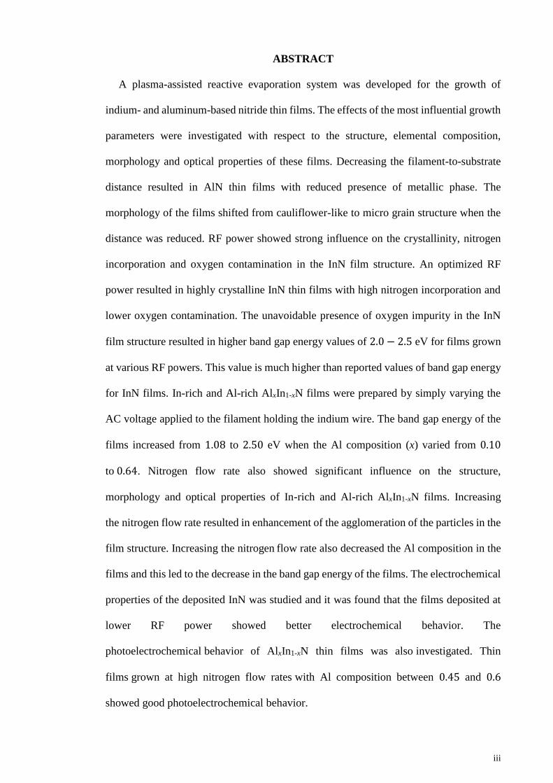
ABSTRACT
A plasma-assisted reactive evaporation system was developed for the growth of
indium- and aluminum-based nitride thin films. The effects of the most influential growth
parameters were investigated with respect to the structure, elemental composition,
morphology and optical properties of these films. Decreasing the filament-to-substrate
distance resulted in AlN thin films with reduced presence of metallic phase. The
morphology of the films shifted from cauliflower-like to micro grain structure when the
distance was reduced. RF power showed strong influence on the crystallinity, nitrogen
incorporation and oxygen contamination in the InN film structure. An optimized RF
power resulted in highly crystalline InN thin films with high nitrogen incorporation and
lower oxygen contamination. The unavoidable presence of oxygen impurity in the InN
film structure resulted in higher band gap energy values of 2.0 − 2.5 eV for films grown
at various RF powers. This value is much higher than reported values of band gap energy
for InN films. In-rich and Al-rich AlxIn1-xN films were prepared by simply varying the
AC voltage applied to the filament holding the indium wire. The band gap energy of the
films increased from 1.08 to 2.50 eV when the Al composition (x) varied from 0.10
to 0.64. Nitrogen flow rate also showed significant influence on the structure,
morphology and optical properties of In-rich and Al-rich AlxIn1-xN films. Increasing
the nitrogen flow rate resulted in enhancement of the agglomeration of the particles in the
film structure. Increasing the nitrogen flow rate also decreased the Al composition in the
films and this led to the decrease in the band gap energy of the films. The electrochemical
properties of the deposited InN was studied and it was found that the films deposited at
lower RF power showed better electrochemical behavior. The
photoelectrochemical behavior of AlxIn1-xN thin films was also investigated. Thin
films grown at high nitrogen flow rates with Al composition between 0.45 and 0.6
showed good photoelectrochemical behavior.
iv
ABSTRAK
Satu sistem penyejatan reaktif dengan bantuan plasma telah dibangunkan untuk
pertumbuhan filem nipis nitrida berasaskan indium dan aluminium. Kesan parameter
pertumbuhan yang paling berpengaruh telah dikaji merujuk kepada struktur, komposisi
unsur, morfologi dan ciri-ciri optik filem-filem ini. Pengurangan jarak di antara filamen
dan substrat menghasilkan penurunan kehadiran fasa logam di dalam filem nipis AlN.
Morfologi filem beralih daripada bentuk seperti kubis bunga kepada struktur bijian mikro
apabila jarak dikurangkan. Kuasa RF menunjukkan pengaruh yang kuat ke atas
penghabluran, penggabungan nitrogen dan pencemaran oksigen dalam struktur filem InN.
Kuasa RF yang optimum menghasilkan filem nipis InN yang tinggi penghablurannya
dengan penggabungan nitrogen yang tinggi dan pencemaran oksigen yang lebih rendah.
Kewujudan pencemaran oksigen yang tidak dapat dielakkan di dalam struktur filem InN
yang tumbuh pada pelbagai kuasa RF menghasilkan jalur tenaga yang lebih tinggi di
dalam lingkungan di antara 2.0 hingga 2.5 eV. Nilai ini adalah jauh lebih tinggi daripada
nilai yang dilaporkan bagi jalur tenaga filem InN. Filem AlxIn1-xN yang kaya-In dan kaya-
Al dapat disediakan dengan hanya mengubah voltan AC dikenakan kepada filamen yang
memegang dawai indium. Jalur jurang tenaga filem meningkat daripada 1.08 kepada 2.50
eV apabila kandungan Al (x) berubah daripada 0.10 kepada 0.64. Kadar aliran nitrogen
juga menunjukkan pengaruh yang signifikan pada struktur, morfologi dan sifat optik bagi
filem-filem AlxIn1-xN yang kaya-In dan kaya-Al. Peningkatan kadar aliran nitrogen
meningkatkan aglomerasi partikel dalam struktur filem. Peningkatan kadar aliran
nitrogen juga menurunkan komposisi Al dalam filem dan ini menyebabkan penurunan
jalur jurang tenaga filem. Sifat elektrokimia InN yang dimendapkan telah dikaji dan
didapati yang filem yang dimendapkan pada kuasa RF yang rendah menunjukkan
perilaku elektrokimia yang lebih baik. Perilaku fotoelektrokimia filem nipis AlxIn1-xN
juga dikaji. Pertumbuhan filem nipis pada kadar aliran nitrogen yang tinggi dengan

v
komposisi Al di antara 0.45 hingga 0.6 menunjukkan perilaku fotoelektrokimia yang
baik.
vi
ACKNOWLEDGEMENTS
In the name of ALLAH, the Most Gracious, the Most Merciful……..
All praises to Allah for His blessing and granting me the straight and ability to complete
this thesis. First and foremost, I offer my deepest gratitude to my supervisor, Professor Datin
Dr. Saadah Abdul Rahman for providing me the opportunity to conduct my PhD. I would like
to thank immensely for her support, advice and patience during this research work. Without
her recommendations and efforts, this thesis would have never been possible to be
completed. Special thanks to my co-supervisor Dr. Goh Boon Tong for guiding me in
laboratory works, giving positive feedbacks on result troubleshooting and also providing all
the materials that are needed in this research.
Many thanks to my colleague Dr. Vottikondala Ganesh for his help and encouragements in
all this period. I extend my thanks to all my teammates for their endless assistance throughout
my experimental work.
I would like to acknowledge government of Malaysia for the grants including Fundamental
Research Grant Scheme (FP009-2013B), University of Malaya, High Impact Research (HIR,
grant: UM.C/HIR/MOHE/SC/06) and University of Malaya Postgraduate Research (PPP,
grant: PG081-2012B) for financial support of my PhD work.
Last but not least, I would like to thank my family and all my friends who made even my little
free time highly enjoyable during these intense three years in Malaysia, for their moral support
and encouragements.
vii
TABLE OF CONTENTS
Abstract ............................................................................................................................ iii
Abstrak ............................................................................................................................. iv
Acknowledgements .......................................................................................................... vi
Table of Contents ............................................................................................................ vii
List of Figures .................................................................................................................. xi
List of Tables................................................................................................................ xviii
List of Symbols and Abbreviations ................................................................................ xix
CHAPTER 1: INTRODUCTION .................................................................................. 1
1.1 Important Properties of Indium- and Aluminum-Based Nitrides ............................ 1
1.2 Application of Indium- and Aluminum-Based Nitrides .......................................... 3
1.3 Growth Techniques of Indium- and Aluminum-Based Nitrides ............................. 4
1.4 Research Problems................................................................................................... 5
1.5 Research Objectives................................................................................................. 6
1.6 Outline of Thesis...................................................................................................... 7
CHAPTER 2: LITERATURE REVIEW ...................................................................... 9
2.1 Introduction.............................................................................................................. 9
2.2 Crystal Structure of Indium- and Aluminum-Based Nitrides .................................. 9
2.3 Band gap and Band Alignment .............................................................................. 11
2.4 Photoelectrochemical Water Splitting Application ............................................... 13
2.5 Growth Methods of Indium- and Aluminum-Based Nitride Thin Films ............... 19
2.5.1 Metalorganic Chemical Vapor Deposition (MOCVD) ............................ 20
2.5.2 Sputtering ................................................................................................. 26
2.5.3 Molecular Beam Epitaxy (MBE).............................................................. 31
viii
2.5.4 Pulsed Laser Deposition (PLD) ................................................................ 37
2.5.5 Plasma-Enhanced Chemical Vapor Deposition (PECVD) ....................... 41
CHAPTER 3: SAMPLE PREPARATION AND CHARACTERIZATION
TECHNIQUES ...……………………………………………………………………...44
3.1 Introduction............................................................................................................ 44
3.2 Research Methodology .......................................................................................... 44
3.3 Deposition of the Thin Films ................................................................................. 47
3.3.1 Deposition System .................................................................................... 47
3.3.2 Pre-heating of Filament ............................................................................ 50
3.3.3 Preparation of Substrates .......................................................................... 51
3.3.4 Pre-deposition Process ............................................................................. 51
3.3.5 Deposition of AlN Thin Films .................................................................. 53
3.3.6 Deposition of InN Thin Films .................................................................. 53
3.3.7 Deposition of AlxIn1-xN Thin Films ......................................................... 54
3.3.8 Annealing Process .................................................................................... 56
3.4 Characterization Techniques ................................................................................. 57
3.4.1 X-ray Diffraction (XRD) .......................................................................... 58
3.4.2 Fourier Transform Infrared (FTIR) Spectroscopy .................................... 60
3.4.3 Micro-Raman Scattering Spectroscopy .................................................... 62
3.4.4 Field Emission Scanning Electron Microscopy (FESEM) and Energy-
Dispersive X-ray (EDX) Spectroscopy .................................................... 65
3.4.5 X-ray Photoelectron Spectroscopy (XPS) ................................................ 66
3.4.6 Surface Profilometry ................................................................................ 68
3.4.7 Ultra-Violet Visible Near-Infrared Spectroscopy .................................... 69
3.5 Electrochemical Study of AlxIn1-xN and InN Thin Films ...................................... 71
3.5.1 Electrochemical Measurement for AlxIn1-xN Thin Films ......................... 71
ix
3.5.2 Electrochemical Measurement for InN Thin Films .................................. 72
CHAPTER 4: ALUMINUM NITRIDE AND INDIUM NITRIDE THIN FILMS BY
PLASMA-ASSISTED REACTIVE EVAPORATION .............................................. 73
4.1 Introduction............................................................................................................ 73
4.2 Effects of Filament-to-Substrate Distance on the Structure, Morphology and
Optical Properties of Aluminum Nitride Thin Films ............................................. 73
4.3 Effects of RF Power on Crystallinity, Morphology, Composition and Optical
Properties of Indium Nitride Thin Films ............................................................... 83
4.4 Summary ................................................................................................................ 93
CHAPTER 5: ALUMINUM INDIUM NITRIDE THIN FILMS: STRUCTURE,
MORPHOLOGY AND OPTICAL PROPERTIES ................................................... 94
5.1 Introduction............................................................................................................ 94
5.2 The Role of Filament Temperature on the Growth of Aluminum Indium Nitride
Thin Films .............................................................................................................. 94
5.3 Effects of Nitrogen Flow Rate on Structure, Morphology, Composition and Optical
Properties of In-rich and Al-rich Aluminum Indium Nitride Thin Films ............ 107
5.4 Effects of Annealing Temperature on the Composition, Structure and Optical
Properties of Aluminum Indium Nitride Thin Films ........................................... 121
5.5 Summary .............................................................................................................. 127
CHAPTER 6: ELECTROCHEMICAL BEHAVIOR OF INDIUM- AND
ALUMINUM-BASED NITRIDE THIN FILMS GROWN BY PLASMA-ASSISTED
REACTIVE EVAPORATION ................................................................................... 128
6.1 Introduction.......................................................................................................... 128
x
6.2 Effects of RF Power on the Electrochemical Properties of Indium Nitride Thin
Films…………………………………………………………………………….128
6.3 Electrochemical and Photoelectrochemical Behaviors of Aluminum Indium Nitride
Thin Films Grown by Plasma-Assisted Dual Source Reactive Evaporation ....... 138
6.4 Summary .............................................................................................................. 147
CHAPTER 7: CONCLUSION AND SUGGESTIONS FOR FUTURE WORKS..148
7.1 Overview.............................................................................................................. 148
7.2 Conclusion ........................................................................................................... 149
7.3 Suggestions for Future Work ............................................................................... 152
References ..................................................................................................................... 154
List of Publications and Papers Presented .................................................................... 171
xi
LIST OF FIGURES
Figure 2.1: Schematic diagram of wurtzite AlN structure (Kuang et al., 2012c). .......... 11
Figure 2.2: Valence band position and offsets for group III-nitrides alloys. From Ref.
(Ramon Collazo & Dietz, 2013). .................................................................................... 13
Figure 2.3: Photoelectrochemical water splitting systems using n-type semiconductor
photoanode (a), p-type semiconductor photocathode (b), and tandem system (c) (Abe,
2010). .............................................................................................................................. 15
Figure 2.4: The SEM results of AlInN films grown by MOCVD method under various
MO gas flow rates of (a) 0.5, (b) 1, and (c) 1.4 standard liters per minute (SLM). The
characters 1, 2, and 3 refer to the substrate positions 92, 118, and 144 mm from MO
entrance. The length of white scale bar is 5 µm (Kang, Yamamoto, Tanaka, Hashimoto,
& Yamamoto, 2009)........................................................................................................ 24
Figure 2.5: Raman spectra AlInN thin films grown by MOCVD at various MO gas flow
rates. From Ref. (Kang, Yamamoto, Tanaka, Hashimoto, & Yamamoto, 2009). .......... 25
Figure 2.6: Transmittance spectra (a) and squared absorption coefficient (b) of sputtered
InxAl1-xN films with different In content (𝑥). From Ref. (He et al., 2010). .................... 30
Figure 2.7: HRXRD spectra of InN thin films grown by PA-MBE at the RF powers of
(a) 350 W and (b) 450 W. From Ref. (M. Kumar et al., 2012) ...................................... 34
Figure 2.8: The SEM image of cross-section (a) and surface (b) of InN films grown by
PA-MB. From Ref. (Kamimura et al., 2007) .................................................................. 36
Figure 2.9: SEM image of AlN thin films grown by PLD method at different N2 pressures;
(a) 100 Torr; (b) 50 Torr; (c) 10 Torr; (d) 1 Torr; (e) 10−1 Torr; (f) 5 × 10⁻² Torr. From
Ref. (Shukla & Khare, 2008). ......................................................................................... 39
Figure 3.1: Flowchart of research methodology involved in this work. ......................... 46
Figure 3.2: A photograph of plasma-assisted reactive evaporation system. ................... 48
Figure 3.3: Schematic diagram of plasma-assisted reactive evaporation system for growth
of AlN and InN thin films. A single tungsten filament holding the In or Al wires are
clamped to stainless steel rods filament holders. ............................................................ 49
Figure 3.4: Schematic diagram of plasma-assisted reactive evaporation system for growth
of AlxIn1-xN thin films. The tungsten filaments holding the In and Al wires are clamped
perpendicular to each other (see the inset image) to stainless steel rod filament holders.
The former is placed above the latter. ............................................................................. 50
xii
Figure 3.5: A photograph of the tube furnace used for the annealing process................ 57
Figure 3.6: (a) The principle of X-ray diffraction and (b) X-ray diffracted beam path in
θ/2θ mode. From Ref (Goh, 2012). ............................................................................... 59
Figure 3.7: A photograph of SIEMENS D5000 X-ray diffractometer............................ 60
Figure 3.8: A photograph of FTIR Perkin-Elmer System 2000. ..................................... 61
Figure 3.9: Schematic diagram of Raman principle. From Ref. (Othman, 2012)........... 63
Figure 3.10: A photograph of Renishaw inVia Raman Microscope. .............................. 63
Figure 3.11: A photograph of JEOL JSM-7600F microscope. ....................................... 66
Figure 3.12: A photograph of PHI Quantera II XPS system........................................... 68
Figure 3.13: A photograph of KLA-Tencor P-6 surface profiler system. ....................... 69
Figure 3.14: A photograph of Lambda 750 UV/Vis/NIR spectrometer.......................... 70
Figure 3.15: Schematic diagram of three-electrode photoelectrochemical cell. ............. 71
Figure 3.16: A photograph of PAR-VersaSTAT 3 electrochemical work station with 150-
W Xenon arc lamp. ......................................................................................................... 72
Figure 4.1: The XRD spectra of AlN thin films grown at different filament-substrate
distances (𝑑𝑓−𝑠). Decrease in 𝑑𝑓−𝑠 shows significant decrease of intensity of metallic
peaks along with preferential AlN growth orientation along the c-axis perpendicular to
the substrate. .................................................................................................................... 75
Figure 4.2: FESEM image of AlN films grown at different filament-substrate distances
(𝑑𝑓−𝑠) (a) 𝑑𝑓−𝑠 = 2.2, (b) 𝑑𝑓−𝑠 = 1.8, (c) 𝑑𝑓−𝑠 = 1.4 and (d) 𝑑𝑓−𝑠 = 1.0 cm with ×5000
magnification. Decreasing the distance the filament distance results in agglomeration of
smaller grains to form cauliflower-shaped grains. .......................................................... 76
Figure 4.3: EDX spectra of AlN films deposited at different filament-substrate distances
(a) 𝑑𝑓−𝑠 = 2.2, (b) 𝑑𝑓−𝑠 = 1.8, (c) 𝑑𝑓−𝑠 = 1.4 and (d) 𝑑𝑓−𝑠 = 1.0 cm. By decreasing
𝑑𝑓−𝑠, intensity of Al decreases whereas that of N increases. .......................................... 77
Figure 4.4: (a) Dependence of the elemental percentage of the AlN films on filament-
substrate distance (𝑑𝑓−𝑠); (b) dependence of N/Al ratio of AlN films on 𝑑𝑓−𝑠. The atomic
concentration of N and Al are greatly affected with respect to 𝑑𝑓−𝑠; Decrease in 𝑑𝑓−𝑠 from
2.2 to 1.0 cm, increases the N/Al ratio to a stoichometric value of 1. (Note: The lines
joining the points are only used as a guide to the eye.) .................................................. 79
xiii
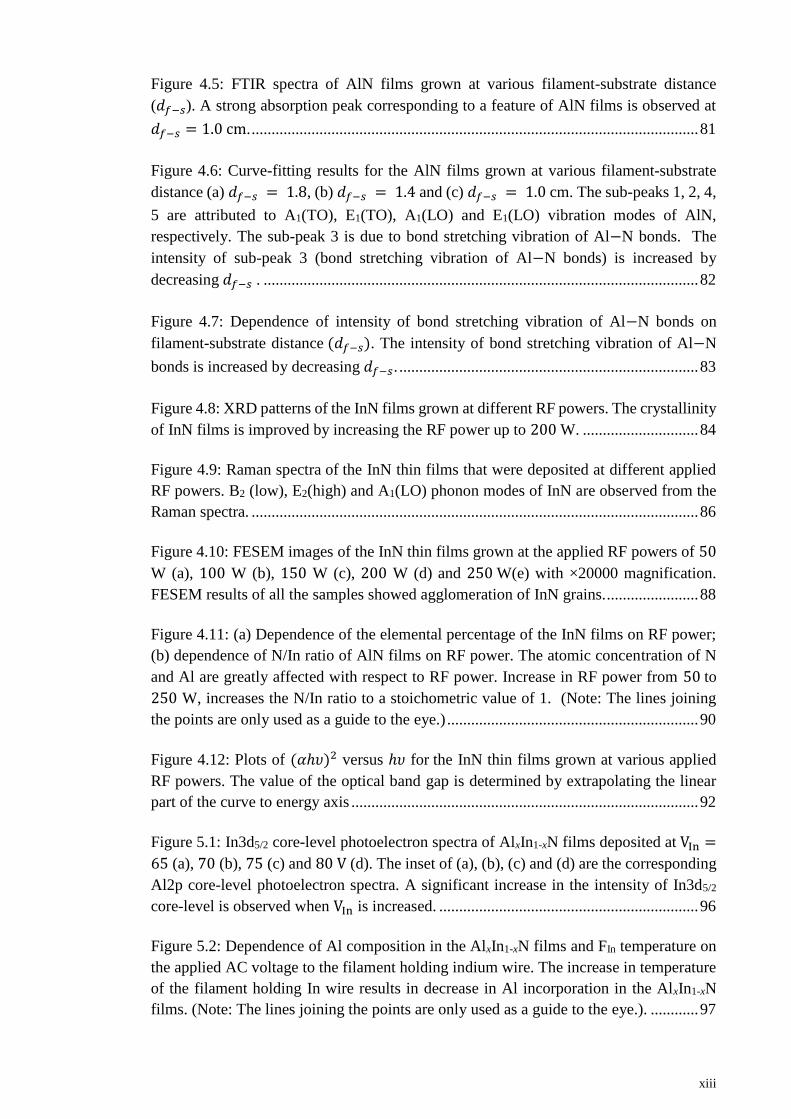
Figure 4.5: FTIR spectra of AlN films grown at various filament-substrate distance
(𝑑𝑓−𝑠). A strong absorption peak corresponding to a feature of AlN films is observed at
𝑑𝑓−𝑠 = 1.0 cm. ................................................................................................................ 81
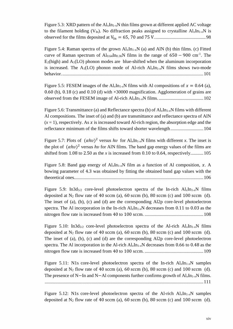
Figure 4.6: Curve-fitting results for the AlN films grown at various filament-substrate
distance (a) 𝑑𝑓−𝑠 = 1.8, (b) 𝑑𝑓−𝑠 = 1.4 and (c) 𝑑𝑓−𝑠 = 1.0 cm. The sub-peaks 1, 2, 4,
5 are attributed to A1(TO), E1(TO), A1(LO) and E1(LO) vibration modes of AlN,
respectively. The sub-peak 3 is due to bond stretching vibration of Al−N bonds. The
intensity of sub-peak 3 (bond stretching vibration of Al−N bonds) is increased by
decreasing 𝑑𝑓−𝑠 . ............................................................................................................. 82
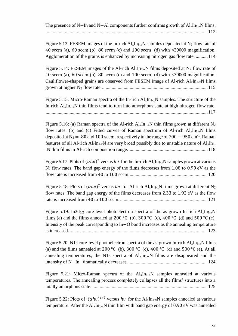
Figure 4.7: Dependence of intensity of bond stretching vibration of Al−N bonds on
filament-substrate distance (𝑑𝑓−𝑠). The intensity of bond stretching vibration of Al−N
bonds is increased by decreasing 𝑑𝑓−𝑠. ........................................................................... 83
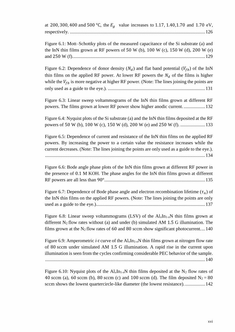
Figure 4.8: XRD patterns of the InN films grown at different RF powers. The crystallinity
of InN films is improved by increasing the RF power up to 200 W. ............................. 84
Figure 4.9: Raman spectra of the InN thin films that were deposited at different applied
RF powers. B2 (low), E2(high) and A1(LO) phonon modes of InN are observed from the
Raman spectra. ................................................................................................................ 86
Figure 4.10: FESEM images of the InN thin films grown at the applied RF powers of 50
W (a), 100 W (b), 150 W (c), 200 W (d) and 250 W(e) with ×20000 magnification.
FESEM results of all the samples showed agglomeration of InN grains. ....................... 88
Figure 4.11: (a) Dependence of the elemental percentage of the InN films on RF power;
(b) dependence of N/In ratio of AlN films on RF power. The atomic concentration of N
and Al are greatly affected with respect to RF power. Increase in RF power from 50 to
250 W, increases the N/In ratio to a stoichometric value of 1. (Note: The lines joining
the points are only used as a guide to the eye.) ............................................................... 90
Figure 4.12: Plots of (𝛼ℎ𝜐)2 versus ℎ𝜐 for the InN thin films grown at various applied
RF powers. The value of the optical band gap is determined by extrapolating the linear
part of the curve to energy axis ....................................................................................... 92
Figure 5.1: In3d5/2 core-level photoelectron spectra of AlxIn1-xN films deposited at VIn =
65 (a), 70 (b), 75 (c) and 80 V (d). The inset of (a), (b), (c) and (d) are the corresponding
Al2p core-level photoelectron spectra. A significant increase in the intensity of In3d5/2
core-level is observed when VIn is increased. ................................................................. 96
Figure 5.2: Dependence of Al composition in the AlxIn1-xN films and FIn temperature on
the applied AC voltage to the filament holding indium wire. The increase in temperature
of the filament holding In wire results in decrease in Al incorporation in the AlxIn1-xN
films. (Note: The lines joining the points are only used as a guide to the eye.). ............ 97
xiv
Figure 5.3: XRD pattern of the AlxIn1-xN thin films grown at different applied AC voltage
to the filament holding (VIn). No diffraction peaks assigned to crystalline AlxIn1-xN is
observed for the films deposited at VIn = 65, 70 and 75 V. ........................................... 98
Figure 5.4: Raman spectra of the grown AlxIn1-xN (a) and AlN (b) thin films. (c) Fitted
curve of Raman spectrum of Al0.64In0.36N films in the range of 650 − 900 cm-1. The
E2(high) and A1(LO) phonon modes are blue-shifted when the aluminum incorporation
is increased. The A1(LO) phonon mode of Al-rich AlxIn1-xN films shows two-mode
behavior. ........................................................................................................................ 101
Figure 5.5: FESEM images of the AlxIn1-xN films with Al compositions of 𝑥 = 0.64 (a),
0.60 (b), 0.18 (c) and 0.10 (d) with ×30000 magnification. Agglomeration of grains are
observed from the FESEM image of Al-rich AlxIn1-xN films. ...................................... 102
Figure 5.6: Transmittance (a) and Reflectance spectra (b) of AlxIn1-xN films with different
Al compositions. The inset of (a) and (b) are transmittance and reflectance spectra of AlN
(x = 1), respectively. As 𝑥 is increased toward Al-rich region, the absorption edge and the
reflectance minimum of the films shifts toward shorter wavelength ............................ 104
Figure 5.7: Plots of (𝛼ℎ𝜐)2 versus ℎ𝜐 for AlxIn1-xN films with different x. The inset is
the plot of (𝛼ℎ𝜐)2 versus ℎ𝜐 for AlN films. The band gap energy values of the films are
shifted from 1.08 to 2.50 as the x is increased from 0.10 to 0.64, respectively........... 105
Figure 5.8: Band gap energy of AlxIn1-xN film as a function of Al composition, 𝑥. A
bowing parameter of 4.3 was obtained by fitting the obtained band gap values with the
theoretical ones.............................................................................................................. 106
Figure 5.9: In3d5/2 core-level photoelectron spectra of the In-rich AlxIn1-xN films
deposited at N2 flow rate of 40 sccm (a), 60 sccm (b), 80 sccm (c) and 100 sccm (d).
The inset of (a), (b), (c) and (d) are the corresponding Al2p core-level photoelectron
spectra. The Al incorporation in the In-rich AlxIn1-xN decreases from 0.11 to 0.03 as the
nitrogen flow rate is increased from 40 to 100 sccm. .................................................. 108
Figure 5.10: In3d5/2 core-level photoelectron spectra of the Al-rich AlxIn1-xN films
deposited at N2 flow rate of 40 sccm (a), 60 sccm (b), 80 sccm (c) and 100 sccm (d).
The inset of (a), (b), (c) and (d) are the corresponding Al2p core-level photoelectron
spectra. The Al incorporation in the Al-rich AlxIn1-xN decreases from 0.66 to 0.48 as the
nitrogen flow rate is increased from 40 to 100 sccm. .................................................. 109
Figure 5.11: N1s core-level photoelectron spectra of the In-rich AlxIn1-xN samples
deposited at N2 flow rate of 40 sccm (a), 60 sccm (b), 80 sccm (c) and 100 sccm (d).
The presence of N−In and N−Al components further confirms growth of AlxIn1-xN films.
....................................................................................................................................... 111
Figure 5.12: N1s core-level photoelectron spectra of the Al-rich AlxIn1-xN samples
deposited at N2 flow rate of 40 sccm (a), 60 sccm (b), 80 sccm (c) and 100 sccm (d).
xv
The presence of N−In and N−Al components further confirms growth of AlxIn1-xN films.
....................................................................................................................................... 112
Figure 5.13: FESEM images of the In-rich AlxIn1-xN samples deposited at N2 flow rate of
40 sccm (a), 60 sccm (b), 80 sccm (c) and 100 sccm (d) with ×30000 magnification.
Agglomeration of the grains is enhanced by increasing nitrogen gas flow rate. .......... 114
Figure 5.14: FESEM images of the Al-rich AlxIn1-xN films deposited at N2 flow rate of
40 sccm (a), 60 sccm (b), 80 sccm (c) and 100 sccm (d) with ×30000 magnification.
Cauliflower-shaped grains are observed from FESEM image of Al-rich AlxIn1-xN films
grown at higher N2 flow rate. ........................................................................................ 115
Figure 5.15: Micro-Raman spectra of the In-rich AlxIn1-xN samples. The structure of the
In-rich AlxIn1-xN thin films tend to turn into amorphous state at high nitrogen flow rate.
....................................................................................................................................... 117
Figure 5.16: (a) Raman spectra of the Al-rich AlxIn1-xN thin films grown at different N2
flow rates. (b) and (c) Fitted curves of Raman spectrum of Al-rich AlxIn1-xN films
deposited at N2 = 80 and 100 sccm, respectively in the range of 700 − 950 cm-1. Raman
features of all Al-rich AlxIn1-xN are very broad possibly due to unstable nature of AlxIn1-
xN thin films in Al-rich composition range. .................................................................. 118
Figure 5.17: Plots of (𝛼ℎ𝜐)2 versus ℎ𝜐 for the In-rich AlxIn1-xN samples grown at various
N2 flow rates. The band gap energy of the films decreases from 1.08 to 0.90 eV as the
flow rate is increased from 40 to 100 sccm. ................................................................. 120
Figure 5.18: Plots of (𝛼ℎ𝜐)2 versus ℎ𝜐 for Al-rich AlxIn1-xN films grown at different N2
flow rates. The band gap energy of the films decreases from 2.33 to 1.92 eV as the flow
rate is increased from 40 to 100 sccm. ......................................................................... 121
Figure 5.19: In3d5/2 core-level photoelectron spectra of the as-grown In-rich AlxIn1-xN
films (a) and the films annealed at 200 °C (b), 300 °C (c), 400 °C (d) and 500 °C (e).
Intensity of the peak corresponding to In−O bond increases as the annealing temperature
is increased. ................................................................................................................... 123
Figure 5.20: N1s core-level photoelectron spectra of the as-grown In-rich AlxIn1-xN films
(a) and the films annealed at 200 °C (b), 300 °C (c), 400 °C (d) and 500 °C (e). At all
annealing temperatures, the N1s spectra of AlxIn1-xN films are disappeared and the
intensity of N−In dramatically decreases. .................................................................. 124
Figure 5.21: Micro-Raman spectra of the AlxIn1-xN samples annealed at various
temperatures. The annealing process completely collapses all the films’ structures into a
totally amorphous state. ................................................................................................ 125
Figure 5.22: Plots of (𝛼ℎ𝜐)1 2⁄ versus ℎ𝜐 for the AlxIn1-xN samples annealed at various
temperature. After the AlxIn1-xN thin film with band gap energy of 0.90 eV was annealed
xvi
at 200, 300, 400 and 500 °C, the 𝐸𝑔 value increases to 1.17, 1.40,1.70 and 1.70 eV,
respectively. .................................................................................................................. 126
Figure 6.1: Mott–Schottky plots of the measured capacitance of the Si substrate (a) and
the InN thin films grown at RF powers of 50 W (b), 100 W (c), 150 W (d), 200 W (e)
and 250 W (f). ............................................................................................................... 129
Figure 6.2: Dependence of donor density (𝑁𝑑) and flat band potential (𝑉𝑓𝑏) of the InN
thin films on the applied RF power. At lower RF powers the 𝑁𝑑 of the films is higher
while the 𝑉𝑓𝑏 is more negative at higher RF power. (Note: The lines joining the points are
only used as a guide to the eye.). .................................................................................. 131
Figure 6.3: Linear sweep voltammograms of the InN thin films grown at different RF
powers. The films grown at lower RF power show higher anodic current. .................. 132
Figure 6.4: Nyquist plots of the Si substrate (a) and the InN thin films deposited at the RF
powers of 50 W (b), 100 W (c), 150 W (d), 200 W (e) and 250 W (f). ..................... 133
Figure 6.5: Dependence of current and resistance of the InN thin films on the applied RF
powers. By increasing the power to a certain value the resistance increases while the
current decreases. (Note: The lines joining the points are only used as a guide to the eye.).
....................................................................................................................................... 134
Figure 6.6: Bode angle phase plots of the InN thin films grown at different RF power in
the presence of 0.1 M KOH. The phase angles for the InN thin films grown at different
RF powers are all less than 90°. .................................................................................... 135
Figure 6.7: Dependence of Bode phase angle and electron recombination lifetime (𝜏𝑛) of
the InN thin films on the applied RF powers. (Note: The lines joining the points are only
used as a guide to the eye.)............................................................................................ 137
Figure 6.8: Linear sweep voltammograms (LSV) of the AlxIn1-xN thin films grown at
different N2 flow rates without (a) and under (b) simulated AM 1.5 G illumination. The
films grown at the N2 flow rates of 60 and 80 sccm show significant photocurrent. ... 140
Figure 6.9: Amperometric i-t curve of the AlxIn1-xN thin films grown at nitrogen flow rate
of 80 sccm under simulated AM 1.5 G illumination. A rapid rise in the current upon
illumination is seen from the cycles confirming considerable PEC behavior of the sample.
....................................................................................................................................... 140
Figure 6.10: Nyquist plots of the AlxIn1-xN thin films deposited at the N2 flow rates of
40 sccm (a), 60 sccm (b), 80 sccm (c) and 100 sccm (d). The film deposited N2 = 80
sccm shows the lowest quartercircle-like diameter (the lowest resistance). ................. 142

xvii
Figure 6.11: Bode angle phase plots of the AlxIn1-xN thin films grown at different N2 flow
rates in the presence of 0.1 M PBS. The obtained Bode phase angles of all AlxIn1-xN films
are less than 90° suggesting that these thin films can be easily permeated by ions. .... 144
Figure 6.12: Mott–Schottky plots of the measured capacitance of the AlxIn1-xN thin films
grown at N2 flow rates of 40 sccm (a), 60 sccm (b), 80 sccm (c) and 100 sccm (d).
Donor densities (𝑁𝑑) and flat band potentials (𝑉𝑓𝑏) of all the films were calculated using
this plots and Equations (6.1) and (6.2). ....................................................................... 146
xviii
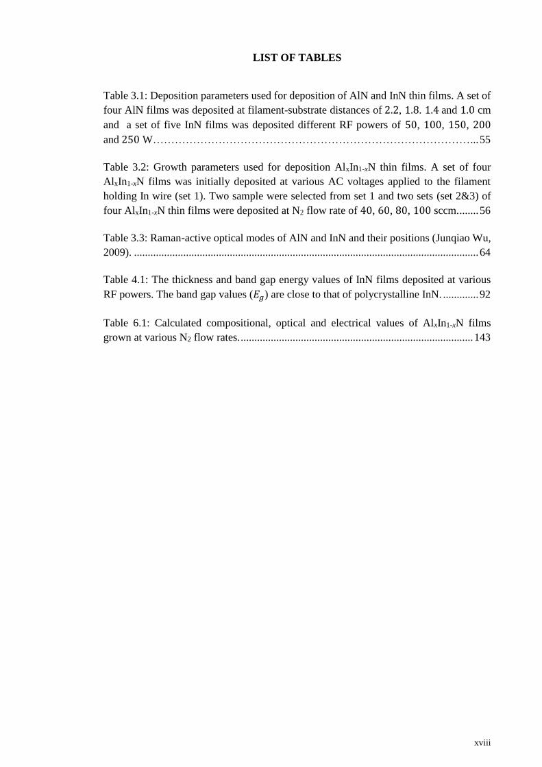
LIST OF TABLES
Table 3.1: Deposition parameters used for deposition of AlN and InN thin films. A set of
four AlN films was deposited at filament-substrate distances of 2.2, 1.8. 1.4 and 1.0 cm
and a set of five InN films was deposited different RF powers of 50, 100, 150, 200
and 250 W…………………………………………………………………………… ... 55
Table 3.2: Growth parameters used for deposition AlxIn1-xN thin films. A set of four
AlxIn1-xN films was initially deposited at various AC voltages applied to the filament
holding In wire (set 1). Two sample were selected from set 1 and two sets (set 2&3) of
four AlxIn1-xN thin films were deposited at N2 flow rate of 40, 60, 80, 100 sccm. ....... 56
Table 3.3: Raman-active optical modes of AlN and InN and their positions (Junqiao Wu,
2009). .............................................................................................................................. 64
Table 4.1: The thickness and band gap energy values of InN films deposited at various
RF powers. The band gap values (𝐸𝑔) are close to that of polycrystalline InN. ............. 92
Table 6.1: Calculated compositional, optical and electrical values of AlxIn1-xN films
grown at various N2 flow rates. ..................................................................................... 143

xix
LIST OF SYMBOLS AND ABBREVIATIONS
A : Interfacial area
AFM : Atomic force microscopy
AlGaN : Aluminum gallium nitride
AlInN : Aluminum indium nitride
AlN : Aluminum nitride
BAW : Bulk acoustic wave
C : Capacitance of the space charge region
°C : Degree centigrade
CBM : Conduction band minimum
CO : Carbon monoxide
CO2 : Carbon dioxide
𝑑𝑓−𝑠 : Filament-to-substrate distance
DUV : Deep ultra-violet
𝜀 : Static dielectric constant
𝜀0 : Permittivity of free space
Eg : Band gap energy
EC : Electrochemical
EDX : Energy-dispersive X-ray spectroscopy
EIS : Electrochemical impedance spectroscopy
FAl : Filament holding (heating) Al wire
FIn : Filament holding (heating) In wire
FESEM : Field emission scanning electron microscopy
FTIR : Fourier transform infrared spectroscopy
FWHM : Full width at half maximum
xx
GaN : Gallium nitride
H2 : Hydrogen
HAADF : High angle annular dark field
HEMT : High-electron-mobility transistor
HRTEM : High-resolution transmission electron microscopy
HRXRD : High-resolution x-ray diffraction
InAs : Indium arsenide
InGaN : Indium gallium nitride
InN : Indium nitride
In2O3 : Indium oxide
ISBT : Inter-subband electron transition
k : Boltzmann’s constant
LED : Light-emitting diode
LD : Laser diode
LO : Longitudinal optical
LSV : Linear sweep voltammogram
LT : Low temperature
MB : Moss-Burstein
MBE : Molecular beam epitaxy
MFC : Mass flow controller
MOCVD : Metalorganic chemical vapor deposition
MQW : Multiple quantum well
MS : Mott–Schottky
N2 : Nitrogen
Nd : Electron donor density
NHE : Normal hydrogen electrode

xxi
NIR : Near-infrared
O2 : Oxygen
PBS : Phosphate buffer solution
PEC : Photoelectrochemical
PECVD : Plasma-enhanced chemical vapor deposition
PL : Photoluminescence
PLD : Pulsed laser deposition
q : Elementary electron charge
𝑅𝑐𝑡 : Charge-transfer resistance
RF : Radio frequency
RHEED : Reflection high-energy electron diffraction
RMS : Root mean square
RTA : Rapid thermal annealing
SAW : Surface acoustic wave
sccm : Standard cubic centimeters per minute
Si : Silicon
SiC : Silicon carbide
Tf : Filament temperature
𝜏𝑛 : Electron recombination lifetime
Ts : Substrate temperature
TMAl : Trimethyl aluminum
TMGa : Trimethyl gallium
TMIn : Trimethyl indium
TO : Transversal optical
VAC : AC voltage
VAl : AC voltage applied to the filament holding Al wire

xxii
Vbias : Applied voltage
Vfb : Flat band potential
VIn : AC voltage applied to the filament holding In wire
VBM : Valence band maximum
Vis : Visible
WO3 : Tungsten oxide
XPS : X-ray photoelectron spectroscopy
XRD : X-ray diffraction
XRF : X-ray fluorescence
1
CHAPTER 1:
INTRODUCTION
1.1 Important Properties of Indium- and Aluminum-Based Nitrides
In the last few years the group III-nitrides have emerged as one of the most important
compound semiconductor materials and have attracted much attention. This is due to their
superior physical properties (G. Li, Wang, Yang, & Wang, 2015; Junqiao Wu, 2009;
Yang et al., 2014) which can be employed in many electronic and opto-electronic devices.
The large differences in the ionic radii and bonding energies of the group III metal cations
give rise to different lattice constants, electron affinities and band gap energies which
challenge the epitaxial deposition of the III-nitrides and their alloys. The most notable of
the group III-nitrides are aluminum nitride (AlN), indium nitride (InN) and their ternary
alloy (aluminum indium nitride, AlInN) which have found applications in various
devices.
AlN has many outstanding properties such as wide band gap energy (6.2 eV),
excellent chemical stability, high hardness, high thermal conductivity, high volume
resistivity and low dielectric constant (Kuang et al., 2012a). Due to strong chemical
bonding, AlN has outstanding physical (high melting point and mechanical strength) and
chemical stability. Since this semiconductor does not have ferroelectric behavior, it is not
required to pole it for piezoelectric sensors/actuators which possess excellent advantages
of low power consumption as compared to capacitive and magnetomotive ones (Tran et
al., 2013). AlN thin films can exist in various crystal orientation and band gap values
depending on the impurity incorporation and the growth parameters such as deposition
temperature and pressure. Investigation of the properties of AlN (and InxAl1-xN) films
under different growth conditions is of importance for application of these films in the
2
electro-acoustic devices as well as for understanding defect mechanism and the origin of
the band gap modulation.
Among the group III-nitrides, InN has the smallest effective mass, smallest band gap
energy (0.64 eV) and highest electron drift velocity which make it particularly suitable
for opto-electronic devices (Ooi et al., 2011; Xu & Yoshikawa, 2003). Up to late 90s,
sputtering method had been mostly used for the growth of InN and the fundamental band
gap energy of the semiconductor was assumed to be 1.9 eV. In fact, A breakthrough
stemmed from the improvement of InN films deposited by molecular beam epitaxy
(MBE) (J. Wu et al., 2002), has led to the revision of InN band gap energy from 1.9 eV
to a much smaller value of 0.64 eV (J. Wu et al., 2003). The new value has been
confirmed theoretically as well (Bechstedt et al., 2003). As a result, it can be concluded
that the full-color spectrum can be achieved by the devices. The dissociation temperature
of InN is quite low (around 600 °C) (X. Wang & Yoshikawa, 2004), hence, to avoid re-
evaporation of nitrogen adatoms the low temperature is required for growth of InN thin
films.
AlxIn1-xN has the widest band gap energy range among all of the group III-nitrides and
has been extensively utilized in opto-electronic field of applications. The increasing
interest is due to its tunable band gap varying remarkably in the range of 0.7-6.2 eV
depending on the amount of indium (or aluminum) constituent (V Yu Davydov et al.,
2002). Hence, varying the composition of AlxIn1-xN film makes it possible to customize
the electronic structures of the alloy films for specific applications. AlxIn1-xN provides
considerable wider band gap energy and lower refractive indices than those of gallium
nitride (GaN) resulting in improved confinement of carriers and photons compared to
gallium-rich aluminum gallium nitride (Ga-rich AlGaN) (Ferhat & Bechstedt, 2002).
However, from the thermodynamic point of view, it is difficult to grow high quality
3
AlxIn1-xN thin film due to the large difference between thermal stability of AlN and InN.
Therefore, few works have been reported so far on the growth of high qualityAlxIn1-xN
compound.
1.2 Application of Indium- and Aluminum-Based Nitrides
Due to the excellent properties of indium and aluminum based nitrides, these
semiconductors have been utilized in numerous applications. AlN is a promising material
for many applications such as bulk acoustic wave (BAW) and surface acoustic wave
(SAW) devices, deep ultra-violet (DUV) light-emitting diodes (LEDs), laser diodes
(LDs), field emission displays and thermoelectric devices (García-Gancedo et al., 2011;
L. a. Guo, Chen, Zhu, Duan, & Ye, 2015; Jeong, Jeon, Lee, & Kim, 2015; Rodríguez-
Madrid et al., 2012). InN has emerged as a potential candidate for many applications
including high-efficiency solar cells, opto-electronic, high speed and high-power
electronic devices (Bhuiyan, Hashimoto, & Yamamoto, 2003). Furthermore, InN has
received remarkable interest for the development of chemical sensors and biosensors due
to its high surface donor density and the corresponding surface electron accumulation,
chemical inertness, and chemical recognition capabilities (Naveed ul Hassan et al., 2013;
Sofikiti et al., 2010). AlxIn1-xN has attracted so much attention for various applications
such as distributed Bragg reflector, field effect transistors, facilitation layers in
pseudomorphic epitaxy and solar cells (Berger, Dadgar, Bläsing, & Krost, 2013;
Monemar, Paskov, & Kasic, 2005; Saidi, Mejri, Baira, & Maaref, 2015; Watson et al.,
2005). In-rich InxAl1-xN thin films with tunable band gap of 0.7-2.4 eV can be used for
multi-junction solar cell devices since this band gap energy range almost covers solar
spectrum (Yamamoto, Islam, Kang, & Hashimoto, 2010).
4
1.3 Growth Techniques of Indium- and Aluminum-Based Nitrides
Nowadays, according to the applications, various epitaxial growth techniques have
been specifically employed for the synthesis of high quality AlN, InN and AlInN
semiconductors under controlled conditions. The most common methods are
Metalorganic Chemical Vapor Deposition (MOCVD), Molecular Beam Epitaxy (MBE),
Pulsed Laser Deposition (PLD), reactive sputtering and Plasma-Enhanced Chemical
Vapor Deposition (PECVD). The deposition process of each method will be described in
detail in chapter 2. Among these methods, sputtering is undoubtedly the most inexpensive
and convenient technique. This technique is versatile in preparing highly crystalline films
economically, which is beneficial for lowering the cost of the device fabrication.
MOCVD and MBE are well-established techniques and are widely utilized for both
research and device production such as LED.
The first AlN and InN compounds were prepared as early as 1907 (Fichter, 1907) and
1932 (Johnson & Parsons, 1931), respectively. However, no remarkable progress was
reported until the end of 1960s. In the late 1960s and early 1970s, development of new
epitaxial deposition methods caused to significant interest in III-nitrides (Manasevit,
Erdmann, & Simpson, 1971; Maruska & Tietjen, 1969; Yoshida, Misawa, & Itoh, 1975)
though quality of the materials was not sufficient for device development. The optical
properties of AlInN/sapphire films were initially investigated in the Al-rich composition
regime in order to use the properties in potential applications (Kubota, Kobayashi, &
Fujimoto, 1989). In the mid-1990s, performance of the nitride devices was improved very
rapidly and commercial attention toward III-nitrides was established by fabrication of
LEDs in the blue and the green regions of the spectrum using MOCVD method.
Nakamura and his colleagues at Nichia Laboratory have improved quality of the
fabricated blue and green LEDs to a level that the devices could be commercialized in the
mid-1990s (Pearton, Zolper, Shul, & Ren, 1999). Following that, numerous works on the
5
fabrication of the optically pumped lasers with high performance were reported (Akasaki
et al., 1995; Schmidt et al., 1996). In recent years, MOCVD technique has been employed
to fabricate high frequency and high power AlInN high-electron-mobility transistors
(HEMTs) with different buffer layers (Kelekci et al., 2012). It has been shown that the
device performance is much better than AlGaN/GaN structures due to enhancement of
spontaneous polarization as a result of AlInN intrinsic properties (Medjdoub et al., 2006).
1.4 Research Problems
Despite the fact that most of the above-mentioned methods led to the growth of high
quality group III-nitride nanostructures, some unwanted drawbacks seem to be
unavoidable using the methods. For instance, in MOCVD process group III-nitride films
are obtained at high substrate temperatures on specified substrates (e.g., sapphire and
GaN) by using a toxic gas such as NH3. Therefore, this method is restricted by the type
and temperature of substrate. The properties of crystalline AlN thin films grown by using
a PLD system are undesirably affected by the repetition frequency of the applied laser
pulses (Sumitani et al., 2010). The sputtered AlN, InN and AlInN films suffer from low
deposition rate which dramatically increases time and cost of device production.
Also, in most cases larger band gap energy values (much higher than 0.7 eV) for InN
and In-rich AlInN films are obtained by sputtering (He et al., 2010; H. F. Liu, Tan,
Dalapati, & Chi, 2012; Valdueza-Felip et al., 2012) although the sputtered films are
highly crystalline. This limits the sputter-deposited InN and In-rich AlInN films for solar
cell applications since the films with narrow band gaps are highly desirable as the base
materials in the solar cell devices. In addition, there have been remarkable disagreements
among the band gap energies measured for AlInN films grown by MOCVD, MBE and
sputtering-based methods. One reason may be that some of the measurements were
6
carried out before the new value of 0.7 eV was established for band gap energy of indium
nitride (InN).
Moreover, in most of the deposition methods listed above, external heating of
substrate with high temperature is required which may cause degradation of the substrate
(H. Cheng et al., 2003) as the whole wafer is exposed to the heating source. Also, these
non-self-heating methods of depositions are costly in terms of energy consumption,
increase thermal budget of manufacture procedure and require long time for heating prior
to the deposition. In other words, preparation of thin films by using a technique that
provides self-heating of substrates during the deposition simplifies the deposition system,
shortens time of the process and as a result makes it possible to gain higher throughout at
low cost.
On the other hand, less works have been devoted to the electrochemical (EC) and
photoelectrochemical (PEC) properties of indium and aluminum based nitride thin films.
The unavoidable surface donor density and the corresponding surface electron
accumulation of InN can be effectively employed for the charge transfer in EC water
splitting application. Also, it has been theoretically shown that Al-rich AlxIn1-xN with a
minimum Al composition (𝑥) of ~0.45 and band gap energy of 1.8 eV is suitable for PEC
water splitting. Therefore, tuning the band gap energy of AlxIn1-xN in the range that meets
water splitting requirement may offer an alternative approach for production of H2 fuel
with PEC water splitting technique.
1.5 Research Objectives
This work focuses on the structure, morphology, optical and electrochemical
properties of indium and aluminum based nitride thin films grown by plasma-assisted
reactive evaporation method. The objectives of this research work are stated below:
7
1. To investigate the effects of radio-frequency (RF) power and filament-to-substrate
distance towards the structure, morphology and composition of InN and AlN thin
films, respectively.
2. To investigate the effects of voltage applied onto filament holding the In wire on
the structure, morphology, composition and optical properties of AlxIn1-xN films
towards tuning the band gap of the films.
3. To investigate the effects of nitrogen gas flow rate on the structure, morphology
and composition of In-rich and Al-rich AlxIn1-xN films.
4. To investigate the effects of annealing on the properties of selected AlxIn1-xN films
for determining the stability of the films for applications in devices.
5. To investigate the EC and PEC performance of InN and Al-rich AlxIn1-xN films,
respectively.
1.6 Outline of Thesis
The thesis is structured as follows. In chapter 2, a literature review based on the
different growth methods of indium- and aluminum-based nitride thin films, their
benefits, drawbacks and the related works are presented. The experimental details and
characterization methods are discussed in chapter 3. This chapter consists of two main
sections. In the first section the sample preparation, the deposition system and process are
described. The second part of the chapter focuses on the analytical apparatus used for
characterization of the grown samples. Also, the corresponding calculations for analysis
of the results are included in the second section of chapter 3. Chapter 4, 5 and 6 are
devoted to obtained results and the corresponding discussions. In chapter 4 the results and
discussions related to growth of AlN and InN thin films are presented in two separated
parts. The first part of chapter 4 focuses on the results and discussions of deposition of
AlN thin films at different filament-to-substrate distances, whereas the second part is
devoted to the results and discussions of growth of InN thin films at different RF powers.
8
Chapter 5 presents the results and discussions corresponding to growth of AlxIn1-xN thin
films. This chapter includes three main sections. The results of the effect of indium-
contained filament (FIn) temperature on the properties of AlxIn1-xN thin films are
presented and discussed in the first part of chapter 5. The second section focuses on the
results and discussions for the deposition of Al-rich and In-rich AlxIn1-xN thin films under
various nitrogen flow rates. The last part of the chapter is devoted to the results and
discussions associated to the annealing AlxIn1-xN thin films at various temperatures.
Chapter 6 of this thesis presents the electrochemical (EC) and photoelectrochemical
(PEC) properties of InN and AlxIn1-xN thin films, respectively. The EC behavior of the
InN films grown under different RF powers is presented in the first part of chapter 6,
whereas the PEC behavior of the Al-rich AlxIn1-xN thin films deposited under various
nitrogen gas flow rates is described in the second part of the chapter. Finally, this thesis
is concluded in chapter 7 which includes summary of the findings and suggestions for
future works.
9
CHAPTER 2:
LITERATURE REVIEW
2.1 Introduction
In chapter 1, the properties of indium- and aluminum-based nitrides, the potential
applications of the semiconductors and the proceeding growth methods for deposition of
these materials were described. A comprehensive review on the previous studies on the
growth and properties of AlN, InN and AlxIn1-xN may help us to get familiar with these
material in order to deposit them by using plasma-assisted reactive evaporation technique.
This chapter begins with a description on the crystal structure of the indium and
aluminum based nitride semiconductors. The next sections gives a detailed information
about the optical properties of the studied semiconductors including the band gap and
band alignment. This leads to an understanding of band positions of AlxIn1-xN at the whole
composition range. Electrochemical (EC) and photoelectrochemical (PEC) Water
Splitting processes, the corresponding requirements for a semiconductor to be used as a
photoelectrode as well as the potential properties of InN and AlxIn1-xN thin films for EC
and PEC water applications will be explained in the fourth section of this chapter. The
chapter ends with a review on the current growth methods of AlN, InN and AlxIn1-xN thin
films.
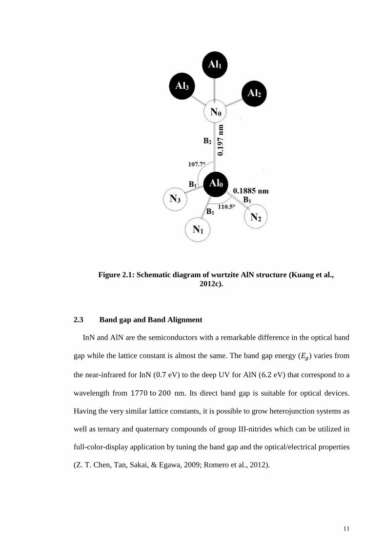
2.2 Crystal Structure of Indium- and Aluminum-Based Nitrides
Under ambient conditions these two nitrides tend to crystallize into two different
structures: wurtzite (hexagonal) and zincblende (cubic). This is an advantage for group
III-nitrides semiconductors over conventional semiconductors such as Si or GaAs, which
have only a diamond or zincblende structure with cubic symmetry. The wurtzite structure
with the space group of P63mc (𝐶6𝑣4 ) is thermodynamically stable. Due to the strong ionic
10
bond between the group-III metal cations and nitrogen anions, the unit cell of the III-
nitrides is distorted from the ideal wurtzite structure causing to a large spontaneous
polarization along the c-axis. In fact, the group III-nitrides are polar crystals because they
do not have a center of symmetry (Daudin, Rouvière, & Arlery, 1996). Due to this
advantage, III-nitrides possess many properties such as pyroelectricity, piezoelectricity
(Kucera et al., 2014; Yalavarthi, Gaddipati, & Ahmed, 2011) and second harmonic
generation (Ivanov, Shubina, Komissarova, & Jmerik, 2014; H. Y. Zhang et al., 1996).
However, the zincblende phase with the space group F43̅m (𝑇𝑑2 ) has been stabilized by
epitaxial growth of thin films. It has been reported that at a hydrostatic pressure of ~ 12
GPa, InN phase is transmitted from the wurtzite into the rocksalt structure with the space
group Fm3m (𝑂ℎ5) (Ueno, Yoshida, Onodera, Shimomura, & Takemura, 1994).
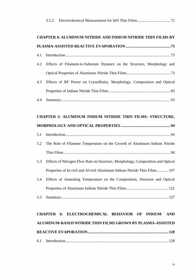
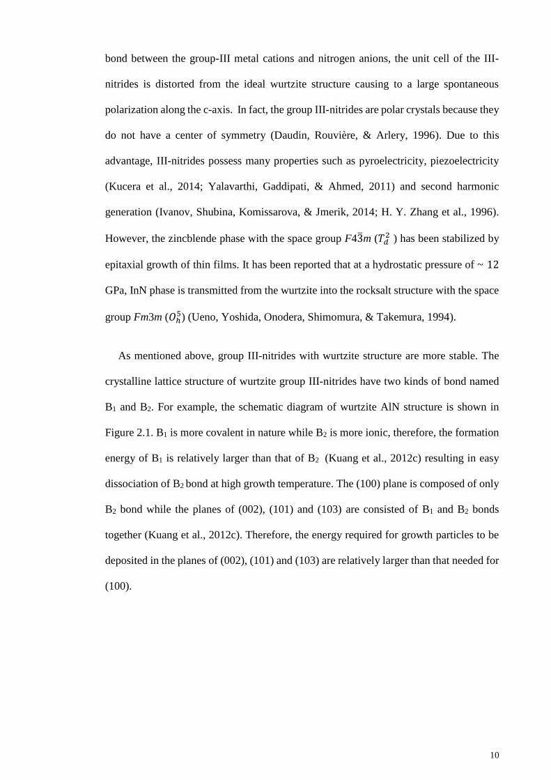
As mentioned above, group III-nitrides with wurtzite structure are more stable. The
crystalline lattice structure of wurtzite group III-nitrides have two kinds of bond named
B1 and B2. For example, the schematic diagram of wurtzite AlN structure is shown in
Figure 2.1. B1 is more covalent in nature while B2 is more ionic, therefore, the formation
energy of B1 is relatively larger than that of B2 (Kuang et al., 2012c) resulting in easy
dissociation of B2 bond at high growth temperature. The (100) plane is composed of only
B2 bond while the planes of (002), (101) and (103) are consisted of B1 and B2 bonds
together (Kuang et al., 2012c). Therefore, the energy required for growth particles to be
deposited in the planes of (002), (101) and (103) are relatively larger than that needed for
(100).
11
Figure 2.1: Schematic diagram of wurtzite AlN structure (Kuang et al.,
2012c).
2.3 Band gap and Band Alignment
InN and AlN are the semiconductors with a remarkable difference in the optical band
gap while the lattice constant is almost the same. The band gap energy (𝐸𝑔) varies from
the near-infrared for InN (0.7 eV) to the deep UV for AlN (6.2 eV) that correspond to a
wavelength from 1770 to 200 nm. Its direct band gap is suitable for optical devices.
Having the very similar lattice constants, it is possible to grow heterojunction systems as
well as ternary and quaternary compounds of group III-nitrides which can be utilized in
full-color-display application by tuning the band gap and the optical/electrical properties
(Z. T. Chen, Tan, Sakai, & Egawa, 2009; Romero et al., 2012).

12
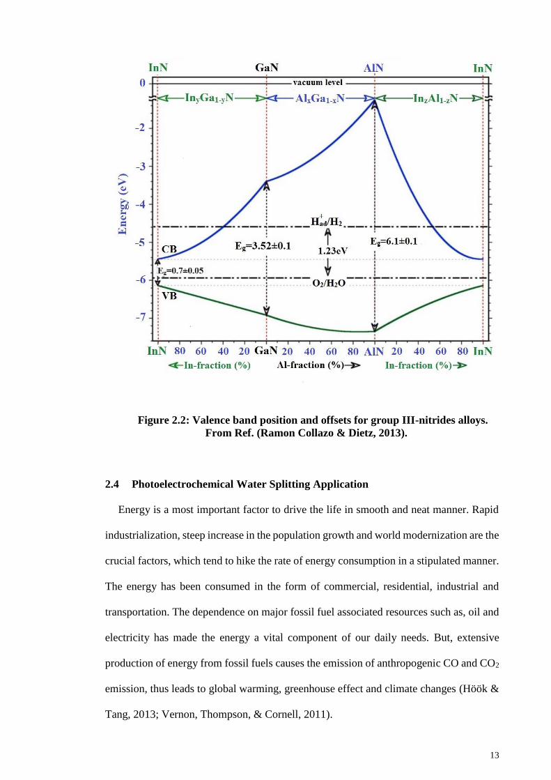
Long before the revision of the band gap value of InN, many theoretical and
experimental investigations has focused on the band offset between group III-nitrides.
Since the revision is mainly on the conduction band-filling effect, previous studies and
values about valence band offset between InN and other nitrides are still considered to be
valid. However, there has been uncertainty on the valence band offset between these
semiconductors due to several reasons such as strain, piezoelectric and spontaneous
polarization effects (Vurgaftman & Meyer, 2003).
Since 1996, different values have been reported for valence band offset between
wurtzite AlN and InN. For instance, on the calculation side 1.25 eV (S. H. Wei & Zunger,
1996), 1.37 eV (Nardelli, Rapcewicz, & Bernholc, 1997) and experimentally 1.52 eV
(King et al., 2007) and 1.80 eV (Martin, Botchkarev, Rockett, & Morkoç, 1996) have
been reported so far. Recently, Ramón Collazo and Nikolaus Dietz (Ramon Collazo &
Dietz, 2013) actively studied Band gap alignments of InN, GaN, AlN and their trinary
alloys. The obtained valence band position and offsets for group III-nitrides alloys is
shown in Figure 2.2. In their studies the valance band maximum (VBM) of wurtzite InN
were found to be ~ 1.2 eV higher than that of AlN whereas the conduction band minimum
(CBM) of wurtzite InN was shown to be 5.0 eV lower than that of AlN. For trinary AlxIn1-
xN, it has been shown that the valence and conduction bands shift linearly and nonlinearly
with Al mole fraction (x), respectively, resulting in band gap bowing of the compound
(Figure 2.2). The observed behavior of valence and conduction band positions in AlxIn1-
xN with different x along with the ability of engineering band gap energy of the
semiconductor may offer a promising approach for production of hydrogen fuel using
PEC water splitting technique. These properties will be discussed in more detailed in the
following section.
13
Figure 2.2: Valence band position and offsets for group III-nitrides alloys.
From Ref. (Ramon Collazo & Dietz, 2013).
2.4 Photoelectrochemical Water Splitting Application
Energy is a most important factor to drive the life in smooth and neat manner. Rapid
industrialization, steep increase in the population growth and world modernization are the
crucial factors, which tend to hike the rate of energy consumption in a stipulated manner.
The energy has been consumed in the form of commercial, residential, industrial and
transportation. The dependence on major fossil fuel associated resources such as, oil and
electricity has made the energy a vital component of our daily needs. But, extensive
production of energy from fossil fuels causes the emission of anthropogenic CO and CO2
emission, thus leads to global warming, greenhouse effect and climate changes (Höök &
Tang, 2013; Vernon, Thompson, & Cornell, 2011).
14
Hydrogen gas generated from a clean and renewable source such as solar energy has
been considered as a main alternative for the conventional energy carriers including fossil
fuels to mitigate financial and environmental problems that associated with fossil fuels
consumptions. Recently, hydrogen gas production via photo-assisted electrolysis
(photoelectrolysis) of water using a light harvesting semiconductor-based system as a
photoelectrochemical (PEC) cell has emerged as one of the most promising methods for
the sustainable, carbon-free and affordable energy supply (Ariffin et al., 2015; Tachibana
et al., 2012). In fact, the simple procedure of solar energy conversion and storage is
photolysis of water with an aid of semiconductor photocatalysts, which act as the light
absorber and energy converter and to store solar energy in the simplest chemical bond,
hydrogen (Cowan & Durrant, 2013).
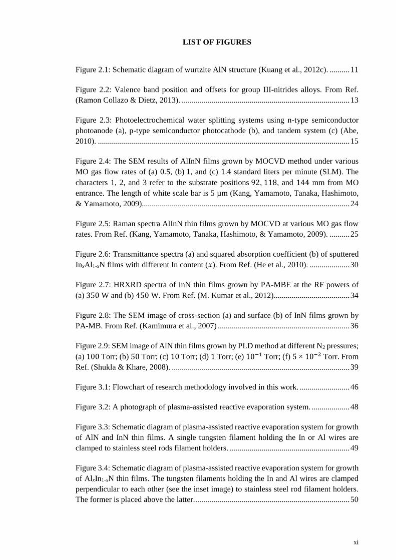
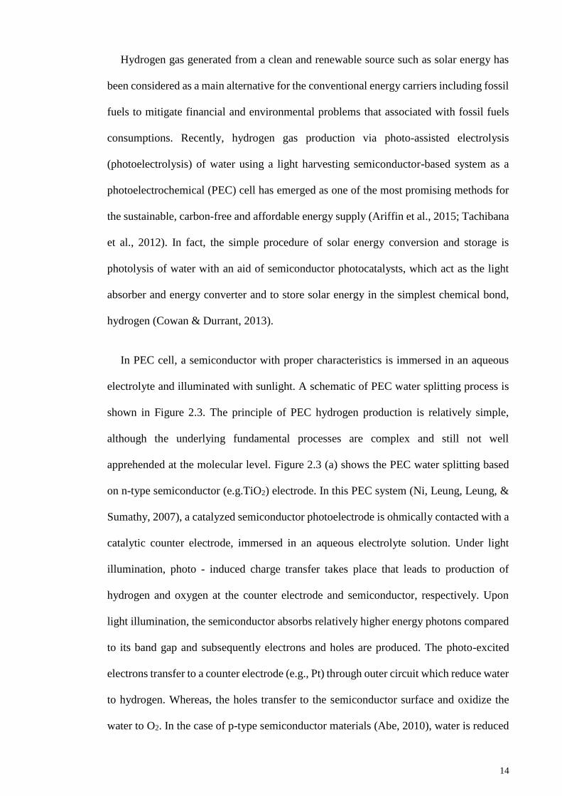
In PEC cell, a semiconductor with proper characteristics is immersed in an aqueous
electrolyte and illuminated with sunlight. A schematic of PEC water splitting process is
shown in Figure 2.3. The principle of PEC hydrogen production is relatively simple,
although the underlying fundamental processes are complex and still not well
apprehended at the molecular level. Figure 2.3 (a) shows the PEC water splitting based
on n-type semiconductor (e.g.TiO2) electrode. In this PEC system (Ni, Leung, Leung, &
Sumathy, 2007), a catalyzed semiconductor photoelectrode is ohmically contacted with a
catalytic counter electrode, immersed in an aqueous electrolyte solution. Under light
illumination, photo - induced charge transfer takes place that leads to production of
hydrogen and oxygen at the counter electrode and semiconductor, respectively. Upon
light illumination, the semiconductor absorbs relatively higher energy photons compared
to its band gap and subsequently electrons and holes are produced. The photo-excited
electrons transfer to a counter electrode (e.g., Pt) through outer circuit which reduce water
to hydrogen. Whereas, the holes transfer to the semiconductor surface and oxidize the
water to O2. In the case of p-type semiconductor materials (Abe, 2010), water is reduced
15
and oxidized at the semiconductor and counter electrode surfaces, respectively (Figure
2.3 (b)). The other system which is called tandem system consists of an n-type
semiconductor electrode with an appropriate p-type semiconductor electrode (Figure 2.3
(c)). There has been numerous investigations on the development of these three systems
with a stable photoelectrode semiconductor that functions efficiently for the production
of hydrogen gas under visible light illumination.
Figure 2.3: Photoelectrochemical water splitting systems using n-type
semiconductor photoanode (a), p-type semiconductor photocathode (b), and
tandem system (c) (Abe, 2010).
In some cases, only an external bias is applied between the working and the counter
electrode to provide charge separation between the electrodes. This system is called
electrochemical (EC) water splitting (Wallys, Hoffmann, Furtmayr, Teubert, & Eickhoff,
2012). The applied external bias excites electrons from valence band to conduction band
creating holes on the valence band. The H2O molecules are oxidized at valence band in
the following reaction:
H2O + h+ ½ O2 + 2H+ (1.1).
The obtained H+ ions are reduced by the excited electrons at conduction band:
16
2H+ + 2e- H2 (1.2).
It should be noted that electron donor density of working electrode is the key factor
determining the resultant anodic current in the EC system. This will be explained more
detailed in chapter 6 of this thesis.
A semiconductor material must satisfy several criteria to be considered as a PEC water
splitter device. (i) Its band gap needs to be a minimum of 1.8 eV to harness visible photons
and to provide the required potential for electrolysis in the single-photoelectrode water
splitting cell system (Weber & Dignam, 1986). (ii) The electron-accepting and electron-
donating states (minority band-edges) and the Fermi level of the material need to
“straddle” the hydrogen gas and oxygen gas production potentials. (iii) The material needs
to have high level of stability in contact with the electrolyte. (iv) It should has high
efficiency to convert energy of acquired photons to separated electron/hole pairs. (v)
Charge transfer at the interface of the material needs to be fast enough to avoid carrier
accumulation at the surface which may cause to shift the band-edges out of the overlap
position.
The suitable band gap for a PEC device is determined by considering two important
aspects of the process: 1. maximizing the absorption of solar photons and 2. Generating
the required energy for water splitting reactions. The highest level of solar absorption
could be attained by narrowing band gap energy of the semiconductor. However, if the
𝐸𝑔 value is too small, the photoelectrode cell will not provide the potential necessary for
electrolysis reactions. The potential difference between the hydrogen-evolving half
reaction (reaction 1.2) and water-oxidation half reaction (reaction 1.1) is 1.229 V. The
water-oxidation and the hydrogen-producing half reactions additionally require 0.275
and 0.050 V over-potential, respectively to proceed at an efficient rate (Kocha & Turner,
1995). For a semiconductor as a PEC water splitting cell, the electron-accepting (or
17
electron-donating) reactions is occurred at Fermi level which is positioned ~ 0.050 −
0.200 eV from the band-edge. As a result, the semiconductor band gap needs to be a
minimum of 1.8 eV to provide the required potential for electrolysis in the single-
photoelectrode water splitting cell system.
Tremendous research works have been reported on metal oxide-based photocatalyst
materials (J. Guo & Chen, 2011; Kudo & Miseki, 2009) since the pioneering work by
Fujishima and Honda who reported the capability of water splitting using TiO2/Pt
photoelectrochemical cell under UV light irradiation in early 1970s (Fujishima & Honda,
1972). However, band gap energy of the most of metal oxide semiconductors is larger
than 3 eV. Therefore it is able to harvest only 4% of light in the solar spectrum. Hence,
the use of metal oxides as photocatalyst materials is undesirably limited by narrow range
of light absorption in the visible spectrum. In addition, a low energy maximum (around
+3 V vs normal hydrogen electrode (NHE) compared to +1.23 V vs NHE for the water-
oxidation reaction) has emerged due to the presence of O 2p orbitals in valence band of
metal oxide materials resulting in a large potential gap between the valence band and
water-oxidation reaction level and, hence, degrades the solar-to-fuel conversion
efficiency (Hwang, Wu, Hahn, Jeong, & Yang, 2012).
On the other hand, group III-nitrides compound semiconductors are more promising
materials for PEC water splitting due to following reasons: (i) III-nitrides have a wide
tunable band gap energy of 0.7– 6.2 eV, which covers the entire solar spectrum and allows
harnessing of visible photons. (ii) Valence band of the metal nitrides consists of N 2p
orbitals which have smaller ionization energies than O 2p orbitals resulting in less positive
valence band maximum potentials than metal oxides (Maeda & Domen, 2007, 2011). (iii)
These photoelectrodes have a high level of inherent chemical stability against corrosion
in aqueous solutions (Maeda, 2011). Indium gallium nitride (InxGa1-xN) with the band gap
18
from 0.7 to 3.4 eV has been proven as a functional photocatalyst for efficient water
splitting. Li et al. (J. Li, Lin, & Jiang, 2008) explored the PEC behavior of InxGa1-xN
epilayers and showed that under white light illumination the photocurrent density strongly
depends on indium (In) incorporation of the epilayers. Stable hydrogen gas production
from water splitting using multiband InxGa1-xN/GaN nanowire heterostructures under a
long-wavelength irradiation (up to 560 nm) were achieved by Kibria et al. (Kibria et al.,
2013). Aryal et al. (Aryal, Pantha, Li, Lin, & Jiang, 2010) have observed H2 generation
in biased p-type InxGa1−xN (0 ≤ x ≤ 0.22) electrodes under white light illumination and
found that the electrodes have an excellent stability in aqueous HBr.
However, very little has been reported so far on electrochemical and
photoelectrochemical properties of InN and AlxIn1-xN semiconductors. For InN, this may
be due to the fact that the band gap energy of InN is now considered to be 0.7 eV not the
previously accepted value of 1.9 eV. Possible reasons for the high band gap value are the
Moss–Burstein (MB) shift, presence of oxygen impurity, and other stoichiometry-related
defects (K. Butcher et al., 2004; T. Shubina et al., 2005). Presence of oxygen enhances
electron donor density on the surface of electrode which is considered as a key factor in
EC process. Therefore, unintentional presence of oxygen in the InN thin films with band
gap energy of ~ 2.0 eV could merge the material as a competitive candidate for EC water
splitting. AlxIn1-xN has a wide tunable band gap of 0.7 to 6.2 eV (V. Yu Davydov et al.,
2002) depending on the indium (or aluminum) composition in the structure. Also, from
Figure 2.2, it can be seen that band-edge potentials of AlxIn1-xN with minimum aluminum
compositions (x) of ∼45% (𝐸𝑔 ∼ 1.8 eV) can straddle the H+/H2 and O2/H2O redox
potentials (Ramón Collazo & Dietz III, 2013) which is another crucial criterion for water
splitting performance as mentioned earlier. Therefore, the ability of engineering band gap
energy of AlxIn1-xN in the range that meets water splitting requirement (1.8 − 2.4 eV) as
19
well as suitable band alignments of AlxIn1-xN (0.45 ≤ x ≤ 0.60) alloys, may offer an
alternative approach for production of H2 fuel with PEC water splitting technique.
2.5 Growth Methods of Indium- and Aluminum-Based Nitride Thin Films
As mentioned earlier, various epitaxial growth techniques have been specifically
employed for the synthesis of high quality AlN, InN and AlInN semiconductors under
controlled conditions. The most common methods are Metalorganic Chemical Vapor
Deposition (MOCVD), Molecular Beam Epitaxy (MBE), Pulsed Laser Deposition (PLD),
reactive sputtering and Plasma-Enhanced Chemical Vapor Deposition (PECVD). Various
substrates have been investigated over the years for the growth or epitaxy of AlN, InN
and AlInN thin films. The lattice mismatch between substrate and the epilayer is very
important in term of the amount of resulting stress in the epilayer. The thermal expansion
coefficient of the substrate is another key factor since a large difference between the
thermal expansion coefficient of the substrate and that of the grown thin films may result
in mechanical stresses and cracks. Three substrates stand out as the most promising for
the growth of III-nitride thin films: sapphire (Al2O3), silicon (Si) and silicon carbide
(SiC). However, glass and quartz have been also used for optical measurement and
devices. Sapphire is most extensively utilized for growth of III-nitride semiconductors
(Kuang et al., 2012c; Skuridina et al., 2014; Y. Zhao et al., 2015). The substrate possesses
outstanding features including high chemical and thermal stability, high availability and
the reasonable cost. However, there are large lattice and thermal mismatch between
sapphire substrate and III-nitride thin films which may cause a compressive strain in the
epilayer upon cooling. Si is the most available substrate in the semiconductor industry.
III–nitride LEDs and LDs are grown on already proceed Si chip to accomplish the
integration of the device with Si electronics. Si is the cheapest among the widely used
substrate for III–nitride growth. However, the substrate suffers from a poor compatibility
with III–nitride crystals and the large lattice mismatch between Si and III–nitrides causes
20
to low quality of the films grown on Si substrate. 6H–SiC (0001) crystal with silicon-
terminated face offers a low lattice mismatch and very close thermal expansion
coefficient with III–nitrides resulting in high quality thin films. The band gap energy of
6H–SiC (0001) substrate is wide (3.05 eV) which makes it promising for application in
high power electronics. The drawbacks of 6H–SiC (0001) are limited availability and
prohibitively high price witch undeniably raise the fabrication cost.
In the following sections, a brief explanation on the above-mentioned growth systems
and the corresponding processes as well as some examples of the reported works are
presented.
2.5.1 Metalorganic Chemical Vapor Deposition (MOCVD)
MOCVD which is also known as metalorganic vapor phase epitaxy (MOVPE) is a
widely used technique for depositing thin layers of atoms on a wafer substrate. One of the
most substantial advantages of MOCVD is its ability to grow high quality epitaxial layers,
each of a precisely controlled thickness, especially for III-V compound semiconductors.
The thickness of the grown multilayer structures is sometimes as thin as a few atomic
layers. Although the growth process is fast and quality of the MOCVD-grown layers is
high, the method has some disadvantages. For example, toxic, volatile and flammable
gases are to be handled and it is not an abrupt process due to gas flow issues and memory
effects. Additionally, in situ observation of films is not possible by using MOCVD
process. The MOCVD process is based on the reaction of chemical compounds in the
vapor phase in the vicinity of the substrate. Trimethylgallium (TMGa),
Trimethylalumium (TMAl), Trimethylindium (TMIn) and ammonia (NH3) are used as
the Ga, Al, In and N precursors, respectively and hydrogen is the carrier gas. The
deposition of III-nitride semiconductors is achieved by decomposing the organic
precursors while they are passing over the hot substrate (Çörekçi, Öztürk, Çakmak,
21
Özçelik, & Özbay, 2012). The substrate temperature depends on the type of growing
semiconductor ranging in 500 − 600 °C for InN and 1100 − 1200 °C for AlN.
Chen et al. (Yiren Chen et al., 2014) have studied the effect of the growth temperature
of AlN nucleation layer (TNL) grown on sapphire substrate on the AlN template using
MOCVD method. Three different TNL of 880 °C, 950 °C and 1020 °C were applied for
growth AlN nucleation layer and it was found that high crystalline AlN template with
uniform and smooth morphology, small full width at half maximum (FWHM) values in
both (0002) and (10–12) planes could be obtained by optimizing the TNL at 950 °C.
FWHM of the grown AlN (0002) and (10–12) planes were in the range of 100 − 300
arcsec for (0002) and 650 − 850 arcsec for (10–12) planes. These results were confirmed
by D.G. Zhao et al. (D. G. Zhao et al., 2012) who proposed a dual AlN buffer layer
structure including an isolated layer (first buffer layer) and a nucleation layer (second
buffer layer) for the growth of high quality AlN films by MOCVD. The obtained results
indicated that by increasing the thickness of nucleation, layer the quality of AlN film
improves. It was additionally found that the thicker the dual AlN buffer layer deposited
in the initial stage, the rougher the surface leading to improved lateral growth of the
following AlN epilayer and then better structural quality the films.
B. Zhang et al. (B. Zhang et al., 2011) successfully deposited non-polar a-plane InN
films by a homemade horizontal-type MOCVD system with GaN buffer, with GaN and
low-temperature (LT) InN buffers, and without any buffer layer. It was shown that all
InN films are in the non-polar (1 1 –2 0) a-plane and the crystal quality of the films is
improved by increasing the growth temperature of GaN buffer layer from 550 to 800 °C.
Furthermore, the author have concluded that the morphology and the crystallography of
a-plane InN are not affected when the LT-InN layer is added, but the intensity of
photoluminescence (PL) spectrum increases significantly. The as-obtained band gap
22
energy for the InN thin films was about 0.75 eV which is in agreement with the recent
reported value.
Numerous works on the growth of AlInN films by MOCVD technique have been
reported since 1989. In the most preparation process of the samples, buffer layer was used
in order to improve the properties of AlInN films for optical devices. S. Yamaguchi et
al.(Yamaguchi et al., 1998) prepared Al1-xInxN films on GaN which was deposited on
AlN-buffered c-plane sapphire substrate. Their structural results showed that Al0.83In0.17N
has the highest crystallinity due to the lowest lattice mismatch of the films with GaN. The
band gap energy of the Al1-xInxN thin films was tuned between 2 and 3 eV by decreasing
the indium incorporation (x) from 0.33 to 0.1 respectively. The band gap value of 2 eV
for In-rich InAlN is not acceptable nowadays due to the revised band gap value of InN
(~ 0.65 eV).
MOCVD system was employed by Sakai et al. (Sakai, Khai, Ichikawa, Egawa, &
Jimbo, 2011) for epitaxial growth and characterization of AlInN/GaN structures on AlN
templates for high-performance ultra-violet photodiodes. Their objectives are to examine
effect of the growth parameters on structural and morphological properties of the
structures as well as to fabricate AlInN-based photodiodes. Higher crystallinity of the
AlInN layers was obtained at low growth pressure, whereas both flat and low pit density
were obtained at the high-temperature growth. By using I-V characteristics, their
fabricated AlInN-based photodiodes showed a leakage current of 48 nA at a reverse
voltage of 5 V and ideality factor of 2.4. Effect of gas flow rate on the structural and
morphological properties of MOCVD-grown In-rich AlInN films has been also reported
(Kang, Yamamoto, Tanaka, Hashimoto, & Yamamoto, 2009).
Kang et al. (Kang, Yamamoto, et al., 2009) showed that by increasing total MO flow
rate or decreasing the distance between the substrate and the MO entrance, the
23
morphology of AlInN films shifts from a pebble-like structure to a grainy one (see Figure
2.4). It was also found that the corresponding Raman features are broadened as the flow
rate increases (Figure 2.5). The author and his co-workers gave a strong experimental
support to the two-mode behavior for A1(LO) phonon in the Raman results of AlInN. As
the last example of MOCVD-grown indium and aluminum based nitride nanostructures,
W.Y. Weng et al. (Weng et al., 2009) have reported the deposition of AlInN epitaxial
layer and the fabrication of AlInN resistive NH3 gas sensor. A rough surface morphology
with quantum dot like nano-islands was found. It was shown that the measured responses
to NH3 gas for the fabricated AlInN sensor (or incremental currents) increase with the
increment of NH3 gas concentration and this responses happened in a short time showing
good response speed of the fabricated sensor. The sensor function was explained by
considering the role of oxygen sorption in electrical transport properties of AlInN
epitaxial layer. It was described that NH3 molecules reacts with the absorbed reactive
oxygen species on AlInN surface resulting in the enhanced conductance of AlInN nano-
islands. These results are highly optimistic for application of AlInN alloys for gas sensing.
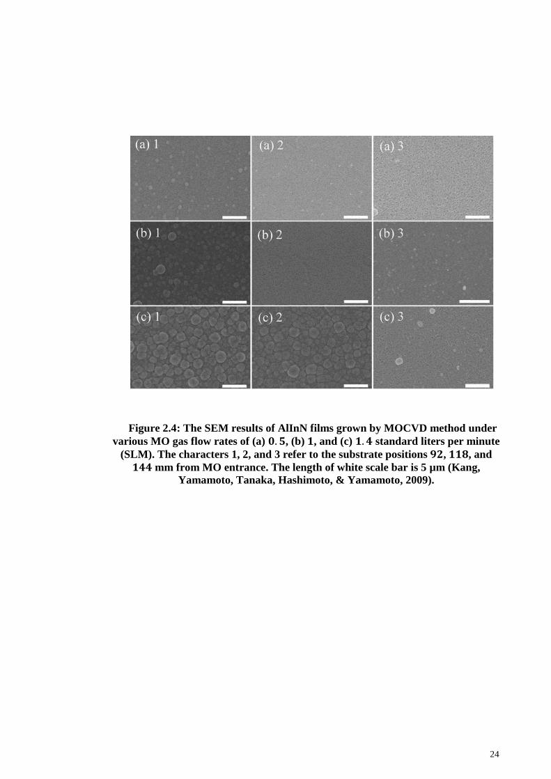
24
Figure 2.4: The SEM results of AlInN films grown by MOCVD method under
various MO gas flow rates of (a) 𝟎. 𝟓, (b) 𝟏, and (c) 𝟏. 𝟒 standard liters per minute
(SLM). The characters 1, 2, and 3 refer to the substrate positions 𝟗𝟐, 𝟏𝟏𝟖, and
𝟏𝟒𝟒 mm from MO entrance. The length of white scale bar is 5 µm (Kang,
Yamamoto, Tanaka, Hashimoto, & Yamamoto, 2009).
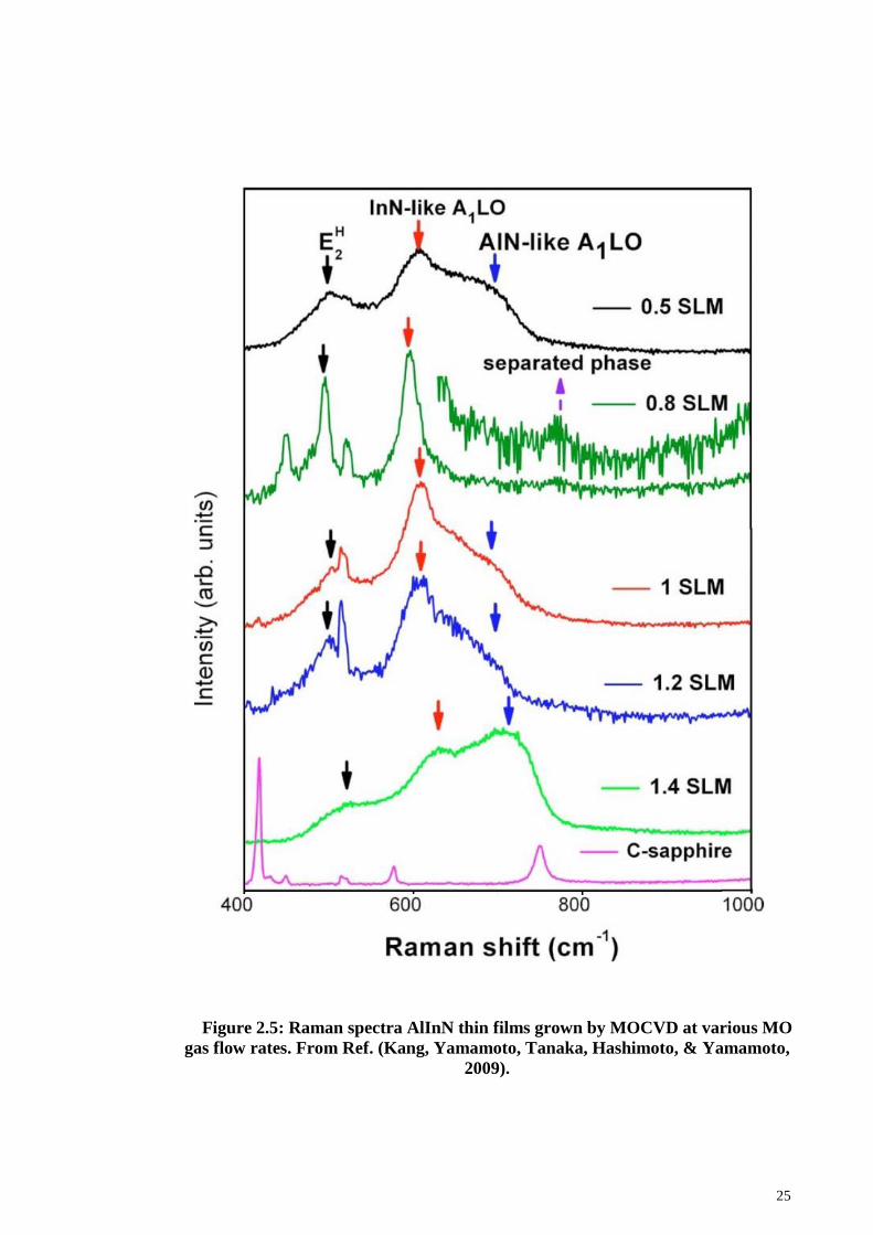
25
Figure 2.5: Raman spectra AlInN thin films grown by MOCVD at various MO
gas flow rates. From Ref. (Kang, Yamamoto, Tanaka, Hashimoto, & Yamamoto,
2009).
26
2.5.2 Sputtering
Sputtering, a well-known technique of depositing thin films of broad range
compositions, is a process whereby atoms are emitted from a solid target (i.e. high quality
Al or In disk) onto a substrate under prolonged bombardment of energetic particles
(Behrisch & Wittmaack, 1983). The energetic particles can be supplied by a plasma
discharge (usually an argon plasma), an ion source, an accelerator, or by a radioactive
material emitting alpha particles. The sputter yield which is defined as the average
number of atoms sputtered from the target per incident ion, depends on the surface
binding energy of atoms in the target, the masses of the ion and target atoms, the energy
of the ion, and the ion incident angle. Radio frequency (RF) magnetron sputtering is
widely employed for deposition of indium- and aluminum-based nitride thin films. Using
this method, the growth of thin films is carried out by deposition of sputtered Al/In
adatoms and N+ ions in N2/Ar plasma environment.
Many studies have been conducted on the growth of AlN and InN thin films using
sputtering-based methods. Kuang et al. (Kuang et al., 2012b) employed RF reactive
magnetron sputtering system to study low-temperature growth of AlN films on 6H–SiC
substrates under various sputtering pressures. Near-stoichiometric ratio of Al/N (1.13: 1)
with few oxygen impurities were found from compositional characterization of the
samples. Their two-dimensional X-ray diffraction patterns (2D-XRD) showed that c-axis
oriented AlN films can be obtained at low working pressures (0.2 − 1.0 Pa). This was
confirmed by Wei et al. (Q.-p. Wei et al., 2014) who have showed that the preferential
growth of AlN thin films is shifted from (002) to (100) direction as the growth pressure
is increased. It was also found that lowering the sputtering pressure is a useful way to
minimize the oxygen contamination into the AlN films. By studying effect of the growth
temperature on the microstructure and morphology of c-axis oriented AlN films, Kuang
et al. (Kuang et al., 2012c) also have showed that the films have high purity and increasing
27
substrate temperature does not have much effect on stoichiometry of the samples, while
the film structure and surface morphology are strongly influenced by the growth
temperature (30 − 700 °C).
Dependence of preferred orientation and surface morphology of AlN films on RF
sputtering powers were investigated by H. Cheng et al. (Hao Cheng & Hing, 2003) and
A.V. Singh et al. (Singh, Chandra, & Bose, 2011). In the former, it was shown that low
RF powers (≤ 300 W) lead to growth of AlN thin films with mix (100), (002) and (101)
orientations, whereas high power (≥ 300 W) is favorable for depositing AlN films with
(1 0 1) preferred orientation. Higher deposition rate and a larger grain size were obtained
by increasing RF sputtering power resulting a rougher surface compared to the
morphology of the films grown at low power. A.V. Singh et al. (Singh et al., 2011)
suggested that by increasing RF sputtering power to 300 W highly c-axis orientated AlN
films can be prepared on various substrates (glass, Si, oxidized Si, Al–SiO2–Si, Cr– SiO2–
Si, and Au–Cr–SiO2–Si) without external substrate heating. The growth of III-nitride thin
films without external substrate heating is one of the most outstanding advantages of
sputtering method which provides fabrication of devices at reduced cost. The authors
also studied the effect of sputtering pressure, ranging from 5 to 20 mTorr, and found that
sputtering pressure (in 5 − 20 mTorr range) weakly influences the preferred growth
which is in good agreement with the results obtained with Kuang et al. (Kuang et al.,
2012a) as mentioned above. The average grain size for different substrates used in the
study was 19 − 26 nm which implies that the grown AlN films were smooth and meet
the requirements of surface acoustic wave (SAW) and Bulk acoustic wave (BAW)
resonators.
The first InN crystal was fabricated by RF sputtering in 1972 (Hovel & Cuomo, 1972)
and up to now large number of sputtering works have been devoted to growth of InN thin
28
films. Most of the works have led to perfect thin films in terms of quality and crystallinity.
Despite this, as mentioned earlier, usually larger 𝐸g values for InN (> 0.7 eV) are
obtained by sputtering which seems to be one major drawback of this technique, at least
in terms of solar cell application because small band gap energies are highly desirable in
solar cell devices. Valdueza-Felip et al. (Valdueza-Felip et al., 2012) deposited InN on
GaN-buffered sapphire substrate by RF sputtering and the measured band gap energy was
1.7 eV. Dixit et al. (Dixit et al., 2009) and Sasaoka et al. (Sasaoka, Mori, Miyazaki, &
Adachi, 2010) obtained the 𝐸g value of around 1.4 eV from rf-magnetron-sputtered InN
film on a (0001) sapphire and corning 7059 glass substrates, respectively. The measured
absorption edge for sputtered InN thin films reported by Cai et al.(Cai et al., 2009) was
observed at around 850 nm which may result in a larger band gap energy than 0.7 eV.
Explanations including the formation of oxynitrides (InOyN1-y with y about 0.1) due to
low efficiency of nitrogen during the layer growth and the spontaneous formation of
needle-like structures upon heteroepitaxial growth of InN (V. Yu Davydov et al., 2002),
the difference in crystallinity (Takashi Matsuoka, Okamoto, Nakao, Harima, & Kurimoto,
2002), quantum-size effects in InN nanocrystals and high-carrier-induced Burstein-Moss
shift (J. Wu et al., 2004) have been proposed for such a large band gap energy shift.
Nevertheless, this is an undeniable disadvantage for sputtering process which limit the
sputter-deposited InN devices for solar cell application as the films with narrow band
gaps can be considered as the absorbing layer of a solar cell.
As compared to AlN and InN, less works have been reported for sputtering-aided
growth of AlInN possibly due to the difficulty of growing AlInN ternary semiconductor.
The origin of this difficulty is the large immiscibility and difference in the thermal
stability between AlN and InN. The first sputter-deposited AlInN alloy was prepared by
Kubota et al. (Kubota et al., 1989) on sapphire substrate in the Al-rich composition regime
with substrate temperature of 500 ̊C. Since then, the optical properties of AlInN films
29
have been studied by employing both low-temperature and high-temperature sputtering
methods (Q. Guo, Tanaka, Nishio, & Ogawa, 2003; He et al., 2010; H. F. Liu et al., 2012;
Peng et al., 1997; Yeh, Wu, & Lan, 2008, 2009). Q. Guo et al. (Q. Guo et al., 2003)
reported growth of AlxIn1-xN with a wide composition range (0 ≤ 𝑥 ≤ 0.40) by reactive
RF magnetron sputtering. The calculated 𝐸g values were 1.5, 2.0, 2.25 and 2.50 eV for
Al compositions (x) 0, 0.05, 0.25 and 0.40, respectively. Large 𝐸g values (much larger
than 0.7 eV) for highly textured InN and In-rich AlInN films with rod-like structures were
also obtained by He et al. (He et al., 2010) who deposited InN and InAlN films on quartz
substrate by magnetron sputtering. The optical results reported by He et al. (He et al.,
2010) are shown in Figure 2.6. The author related the large shift of the measured 𝐸g values
to high carrier concentration in the films structure. Liu et al. (H. F. Liu et al., 2012) have
reported columnar growth of Al0.278In0.722N thin films with no phase separation by radio
frequency magnetron sputtering. The room-temperature photoluminescence emission and
the optical absorption edge were obtained at 1.875 and 2.102 eV which were larger than
the theoretically-predicted band gap energy of the alloy. The deviation of the band gap
energy was attributed to the band-filling effect induced by high electron density in the
heterostructure.
As mentioned earlier, one common reason reported for the discrepancy in band gap
energy of InN is the Burstein–Moss effect by which the band gap energy would be
increased with higher carrier concentration (He et al., 2010) according to the following
equation:
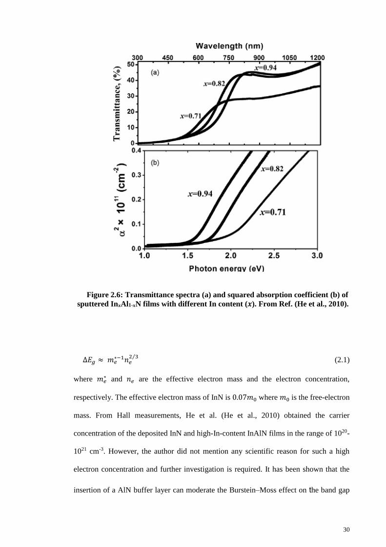
30
Figure 2.6: Transmittance spectra (a) and squared absorption coefficient (b) of
sputtered InxAl1-xN films with different In content (𝒙). From Ref. (He et al., 2010).
∆𝐸𝑔 ≈ 𝑚𝑒∗−1𝑛𝑒
2 3⁄ (2.1)
where 𝑚𝑒∗ and 𝑛𝑒 are the effective electron mass and the electron concentration,
respectively. The effective electron mass of InN is 0.07𝑚0 where 𝑚0 is the free-electron
mass. From Hall measurements, He et al. (He et al., 2010) obtained the carrier
concentration of the deposited InN and high-In-content InAlN films in the range of 1020-
1021 cm-3. However, the author did not mention any scientific reason for such a high
electron concentration and further investigation is required. It has been shown that the
insertion of a AlN buffer layer can moderate the Burstein–Moss effect on the band gap
31
energy of InN (Yeh et al., 2008). T.-S. Yeh et al. (Yeh et al., 2008) showed that the carrier
concentration of In-rich AlxIn1-xN/AlN/glass films with 𝑥 = 0.12, 0.26 and 0.36 were
3 × 10²⁰, 6 × 10¹⁹ and 3 × 10¹⁸, respectively.
In another work, both Al-rich (Al0.55In0.45N) and In-rich (Al0.36In0.64N) films were
deposited on glass substrate with and without AlN buffer layer by T.-S. Yeh et al. (Yeh
et al., 2009) using pulsed-dc reactive sputtering and the structural and optical properties
of the films were investigated at various substrate temperatures. The structural analysis
showed that by increasing substrate temperature from 200 ̊C to 400 ̊C, the crystallinity
of AlInN films grown directly on the glass substrate improved. However, at high
temperature (≥ 300 C̊) oxygen contamination was detected from XPS analysis of the
samples. The author et al. (Yeh et al., 2009) suggested that by using AlN buffer layer not
only the crystallinity of AlInN films was considerably improved but also no oxygen
contamination was observed. Based on the above-mentioned results, it can be concluded
that the lattice-matched buffer layer can play a crucial rule in crystallinity, quality, optical
and electrical properties of AlInN films.
2.5.3 Molecular Beam Epitaxy (MBE)
Molecular Beam Epitaxy (MBE) combined the knowledge of “surface physics” and
“ion propulsion technology” to develop a new method for the deposition of single crystals
and was initially employed by A. Y. Cho (A. Y. Cho, 1970) for epitaxial growth of GaAs
thin films. Nowadays, this technique is widely utilized in the manufacturing of
semiconductor devices such as high-electron-mobility transistors (HEMTs) for cellular
phones and WiFi. MBE takes place in a chamber under high vacuum or ultra-high vacuum
(~ 10−10 mbar) and without carrier gases. Hence, the highest purity of the grown films
is achievable using this method.
32
In MBE processing, ultra-pure elements such as indium and arsenic are slowly
sublimed in separated quasi-Knudsen effusion cells. The gaseous reactants are then
ejected to the chamber and condensed on a heated substrate to grow single crystalline
InAs films. For the case of indium- and aluminum-based nitride semiconductors, NH3
(ammonia) is used as the nitrogen source but sometimes MBE is attached to a RF plasma
cell to ionize N2 molecules and generate nitrogen reactants. This system is called plasma-
assisted molecular beam epitaxy (PA-MBE). The term “beam” refers to the fact that the
reactants are directed separately to the substrate and do not interact with each other until
they deposit on the substrate. One of the most substantial advantages of MBE is precise
and in situ control of the thickness of each layer during the deposition process using
reflection high-energy electron diffraction (RHEED) for monitoring the growth of the
monolayers. However, this technique has several unavoidable drawbacks. Multi-stage
vacuum system is required to provide ultra-high vacuum. The deposition rate is low
(around 500 nm per hour) compared to other methods such as MOCVD. Moreover, the
maintenance and replacement of the source materials inside the ultra-high vacuum
chamber is time-taking and somehow tedious.
Many researchers have reported the growth, characterization and application of AlN
films by MBE. Ammonia MBE was employed by V.G. Mansurov et al. (Mansurov et al.,
2007) to investigate the effect of sapphire surface nitridation on morphology of the grown
AlN. It was shown that modification of nitridated sapphire substrate by depositing 1 − 2
monolayers of Al together with ammonia flux treatment can improve the morphology of
the subsequent AlN layers. B. Liu et al. (B. Liu, Gao, Wu, & Liu, 2009) prepared single
crystalline AlN thin films on Al2O3 at high temperature of 785 ̊C using RF-MBE and
studied the effect of rapid thermal annealing (RTA) on structural and morphological
properties of the films for high frequency and high power devices.
33
The AlN films became smoother with the increase of annealing temperature and the
best crystallinity (the minimum FWHM of AlN (002) rocking curve) was found at the
annealing temperature of 1000 ̊C. Mohd Yusoff et al. (Mohd Yusoff et al., 2013)
investigated microstructure properties of AlN/GaN/AlN heterostructures by using
plasma-assisted MBE and claimed that the crystalline quality of the epilayers was
improved compared to previously reported results due to decreased defects of threading
dislocations with a screw component. However the reported EDX results showed that the
films have high content of Al. C. Flynn and L.W. Sim (Flynn & Sim, 2015) proposed
that phosphoric acid (H3PO4) is very useful for removing excess Al from the AlN surface.
It was shown that if the MBE-grown AlN films are immersed in H3PO4 heated to 70 °C
for 10 min hexagonal etch pits are formed in the AlN films and the metallic Al particles
are removed. The effect of phosphoric acid on the surface morphology of AlN becomes
much more important when it was found that excess Al on the surface of the films caused
an error of up to 7.6% in the AlN thickness. The study is very promising in improving
the quality and morphology of AlN films.
MBE has been also employed by many researchers for growth of InN films. The
revised band gap energy of InN (0.7 eV) was obtained by growth of the semiconductor
using MBE method in 2003 (J. Wu et al., 2003). Since then, this value has been confirmed
by most of the MBE works under different growth conditions. Shih et al. (Shih, Lo, Pang,
& Hiseh, 2010) investigated growth of InN thin films on O-polar ZnO substrate under
various N/In flow ratios. The author have observed that by decreasing the N/In ratio,
surface morphology the PA-MBE-grown films changed from 3D to 2D. From the SEM
and TEM imaging it was shown that the formed In2O3 buffer layer between ZnO substrate
and InN films can significantly improve the morphology of the InN epilayer. However,
the obtained threshold energy of optical transmission was around was around 1.9 eV
much larger than the recently accepted value of 0.7 eV.
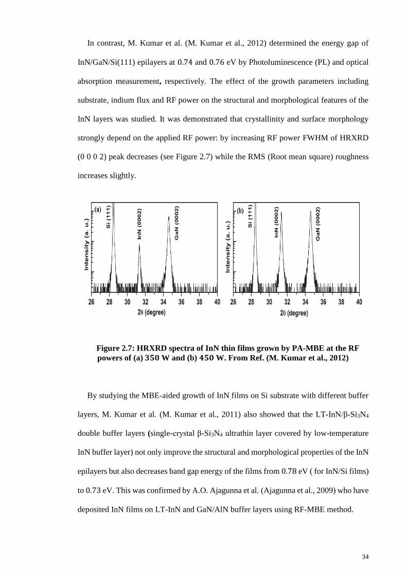
34
In contrast, M. Kumar et al. (M. Kumar et al., 2012) determined the energy gap of
InN/GaN/Si(111) epilayers at 0.74 and 0.76 eV by Photoluminescence (PL) and optical
absorption measurement, respectively. The effect of the growth parameters including
substrate, indium flux and RF power on the structural and morphological features of the
InN layers was studied. It was demonstrated that crystallinity and surface morphology
strongly depend on the applied RF power: by increasing RF power FWHM of HRXRD
(0 0 0 2) peak decreases (see Figure 2.7) while the RMS (Root mean square) roughness
increases slightly.
Figure 2.7: HRXRD spectra of InN thin films grown by PA-MBE at the RF
powers of (a) 𝟑𝟓𝟎 W and (b) 𝟒𝟓𝟎 W. From Ref. (M. Kumar et al., 2012)
By studying the MBE-aided growth of InN films on Si substrate with different buffer
layers, M. Kumar et al. (M. Kumar et al., 2011) also showed that the LT-InN/β-Si3N4
double buffer layers (single-crystal β-Si3N4 ultrathin layer covered by low-temperature
InN buffer layer) not only improve the structural and morphological properties of the InN
epilayers but also decreases band gap energy of the films from 0.78 eV ( for InN/Si films)
to 0.73 eV. This was confirmed by A.O. Ajagunna et al. (Ajagunna et al., 2009) who have
deposited InN films on LT-InN and GaN/AlN buffer layers using RF-MBE method.
35
Numerous works have been devoted to growth of AlInN ternary alloys by PA-MBE
and the corresponding optical properties have been investigated. However, the growth of
high quality AlInN films is still challenging, due to large differences in bonding energy,
lattice constant as well as optimum growth temperature between AlN and InN (Takashi
Matsuoka, 1997). Lukitsch et al. (Lukitsch et al., 2001) have obtained epitaxial Al1-xInxN
films with the whole composition range (0≤ x ≤1) by PA-MBE. However, the measured
band gap energy for the In-rich films (x=0.88) was around 1.8 eV, very near to the old
energy gap of InN. The reason of such a high band gap value probably is that this study
was carried out before the confirmation of 0.7 eV for InN band gap energy.
About four years after improvment of InN band gap value from 1.9 to 0.63 eV, W.
Terashima et al. (Terashima, Che, Ishitani, & Yoshikawa, 2006) reported deposition of
N-polar AlxIn1-xN films with the whole composition range on N-polar GaN substrate at
the substrate temperature of 550 °C without any phase separation. The band gap value of
the PA-MBE-grown Al0.12In0.88N films was almost half the value obtained by Lukitsch et
al. (Lukitsch et al., 2001). The effect of substrate temperature on the structural and
compositional properties of Al0.56In0.44N films were also investigated by Terashima et al.
(Terashima et al., 2006) and it was shown that by increasing the temperature from 500 °C
to 600 °C, the Al incorporation in the films structure decreases by 0.08 and the films
become poorly crystalline possibly due to the enhanced phase separation in the alloys
prepared at higher temperature. However, the reported compositional behavior was
contravened by Fernández-Garrido and his colleagues (Fernández-Garrido, Gačević, &
Calleja, 2008) who showed In incorporation into the PA-MBE-grown AlInN films
decreases with the substrate temperature. Fernández-Garrido and his co-workers
(Fernández-Garrido et al., 2008) explained that the observed behavior is due to thermal
InN decomposition while no justification was reported by Terashima et al. (Terashima et
al., 2006) for the reverse trend.
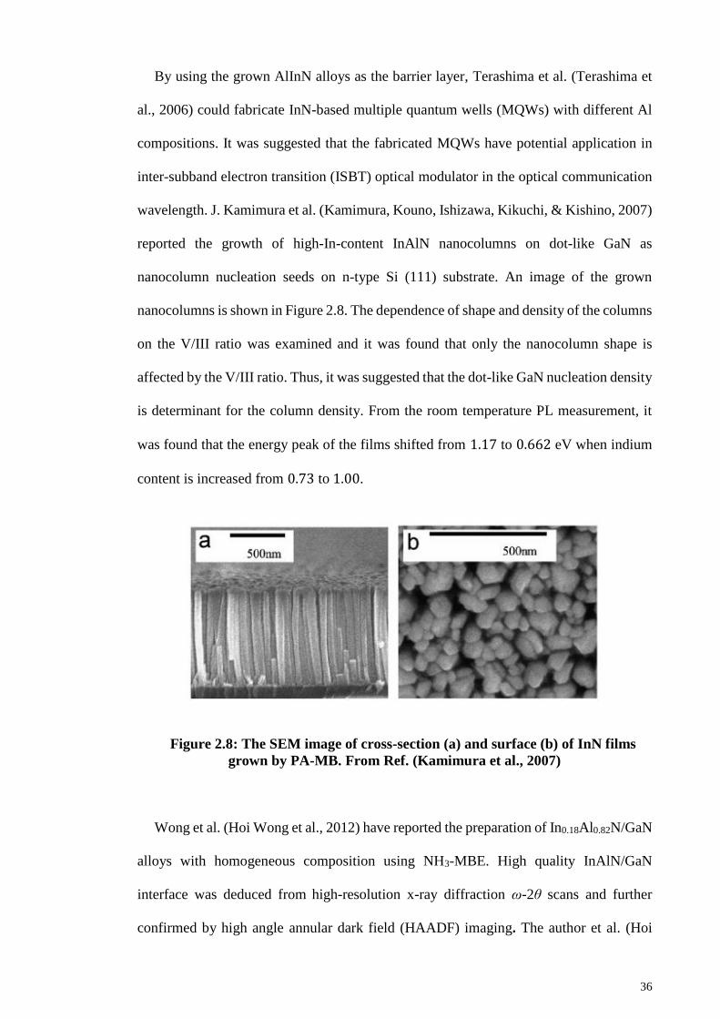
36
By using the grown AlInN alloys as the barrier layer, Terashima et al. (Terashima et
al., 2006) could fabricate InN-based multiple quantum wells (MQWs) with different Al
compositions. It was suggested that the fabricated MQWs have potential application in
inter-subband electron transition (ISBT) optical modulator in the optical communication
wavelength. J. Kamimura et al. (Kamimura, Kouno, Ishizawa, Kikuchi, & Kishino, 2007)
reported the growth of high-In-content InAlN nanocolumns on dot-like GaN as
nanocolumn nucleation seeds on n-type Si (111) substrate. An image of the grown
nanocolumns is shown in Figure 2.8. The dependence of shape and density of the columns
on the V/III ratio was examined and it was found that only the nanocolumn shape is
affected by the V/III ratio. Thus, it was suggested that the dot-like GaN nucleation density
is determinant for the column density. From the room temperature PL measurement, it
was found that the energy peak of the films shifted from 1.17 to 0.662 eV when indium
content is increased from 0.73 to 1.00.
Figure 2.8: The SEM image of cross-section (a) and surface (b) of InN films
grown by PA-MB. From Ref. (Kamimura et al., 2007)
Wong et al. (Hoi Wong et al., 2012) have reported the preparation of In0.18Al0.82N/GaN
alloys with homogeneous composition using NH3-MBE. High quality InAlN/GaN
interface was deduced from high-resolution x-ray diffraction ω-2θ scans and further
confirmed by high angle annular dark field (HAADF) imaging. The author et al. (Hoi
37
Wong et al., 2012) investigated compositional uniformity of the samples by Energy-
dispersive x-ray spectroscopy (EDXS) on parallel to as well as across the InAlN/GaN
interface and demonstrated that the deposited films are homogenous in composition.
Moreover, the reported atomic force microscopy (AFM) results showed that the thin
AlInN has an ultra-smooth hillock-like morphology with the RMS roughness of ~ 2 nm.
However, no optical characterization and measurement (e.g. optical band gap energy of
the grown Al-rich AlInN films) was provided.
2.5.4 Pulsed Laser Deposition (PLD)
PLD is a thin films growth method where a target of the material is vaporized by a
high-power pulsed laser beam in a vacuum or a background gas. For III-nitride cases,
pure aluminum/indium and nitrogen are used as the target and background gas,
respectively. Although the basic-setup of the technique is simple, the overall process
including the physical phenomena occurred during laser-target interaction, dynamic of
the developed plasma and nucleation of the deposited adatoms are somehow complicated.
In fact, PLD is carried out in following steps: first, the laser pulse is absorbed by the target
and its energy is converted into thermal, chemical and mechanical energy leading to
ablation and evaporation of the material, ionization of the background gas and formation
of plasma ambient. Then, the plasma bulk is spatially distributed over the chamber and in
vicinity of the substrate depending on the background pressure. At the third stage, the
ablated species are accelerated toward the substrate surface with high energy which may
cause to re-sputtering of the deposited particles. The collisions between the ablated
species from the target and the re-sputtered particles determine condensation of particles
on the substrate surface and as a result growth of the film. Finally, nucleation of the
adatoms and growth process of the films are occurred depending on the growth
parameters including laser energy and fluency, substrate temperature and background
pressure.
38
Pulsed laser deposition of AlN thin films has been reported by large number of
researchers. However, the number of the works is less than MOCVD-, sputtering- and
MBE-based works showing that PLD is still on its infant. Nevertheless, the method is
surprisingly being developed as most of the PLD-based works have been published in
recent years. G. Shukla, A. Khare (Shukla & Khare, 2008) studied effect of the low N2
pressure regime (5 × 10⁻² and 10−1 Torr) and the high N2 pressure regime (10 and 100
Torr) on properties of pulsed laser deposited AlN films and found that the preferred
orientation of AlN films changes from (101) at high N2 pressure to (002) at low N2
pressure. Accordingly, the films deposited at high N2 pressure was rougher than that
grown at the low pressure regime (see Figure 2.9). By considering the plasma dynamics
during the deposition, the authors explained that the more energetic species in low N2
pressure have enhanced mobility on the substrate surface leading to rearranging of the
film surface and filling the voids while increased number of collisions raised from higher
nitrogen pressure results in a variation in the growth direction of AlN thin films. At low
deposition pressure, the preferred orientation of AlN thin film was (002) while by
increasing the N2 pressure the growth direction of AlN shifted to (101). However, G.
Shukla, A. Khare (Shukla & Khare, 2008) mentioned that they could not grow AlN thin
films at N2 pressure below 10−2 Torr.
Dependence of surface morphology and crystallinity orientation of pulsed laser
deposited AlN films on nitrogen pressure was also confirmed by S. Bakalova et al
(Bakalova et al., 2009) and Wang et al. (Z. P. Wang, Morimoto, Kawae, Ito, & Masugata,
2011). The former synthesized AlN films at very low N2 pressure (7.5 × 10⁻⁴ to 7.5 ×
10−2 Torr) using bulk AlN as the target. The obtained tendency reported in both works
was: by increasing the pressure the size of AlN particles decreases resulting in smooth
surface. The reason of this result was correlated with the reduced growth rate at high
nitrogen pressure. The influence of target–substrate distance in PLD system on
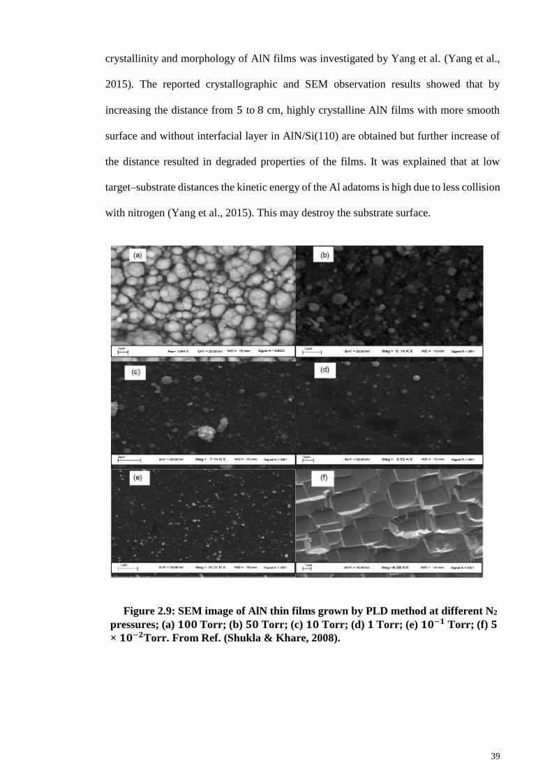
39
crystallinity and morphology of AlN films was investigated by Yang et al. (Yang et al.,
2015). The reported crystallographic and SEM observation results showed that by
increasing the distance from 5 to 8 cm, highly crystalline AlN films with more smooth
surface and without interfacial layer in AlN/Si(110) are obtained but further increase of
the distance resulted in degraded properties of the films. It was explained that at low
target–substrate distances the kinetic energy of the Al adatoms is high due to less collision
with nitrogen (Yang et al., 2015). This may destroy the substrate surface.
Figure 2.9: SEM image of AlN thin films grown by PLD method at different N2
pressures; (a) 𝟏𝟎𝟎 Torr; (b) 𝟓𝟎 Torr; (c) 𝟏𝟎 Torr; (d) 𝟏 Torr; (e) 𝟏𝟎−𝟏 Torr; (f) 𝟓
× 𝟏𝟎−𝟐Torr. From Ref. (Shukla & Khare, 2008).
40
On the other hand, at large distances, the kinetic energy of the adatoms is not sufficient
for diffusion of the adatoms into their lowest energy nucleation sites. The reported results
suggested that there is an optimum target–substrate distance for growth of AlN films
using PLD method. Optical properties of PLD-grown AlN films were studied by C.
Ristoscu et al. (Ristoscu, Ducu, Socol, Craciunoiu, & Mihailescu, 2005) and F. Chale-
Lara et al. (Chale-Lara, Farias, Huerta-Escamilla, & Xiao, 2009). F. Chale-Lara et al.
(Chale-Lara et al., 2009) employed PLD system for obtaining high quality AlN thin films
under different nitrogen pressure at relatively high temperature. It was suggested that the
most influential PLD parameter, especially for optical characterization, is the nitrogen
pressure meaning that there is an optimized gas pressure under which the optical
properties of AlN films improve significantly. However, there is still lack of information
on optical investigation of PLD-grown AlN films.
Successful growth of InN films by PLD method has been also reported, although the
number of works is not comparable with MOCVD, sputtering and MBE. Direct
deposition of InN films on sapphire (0001) substrate along with the influence of laser
intensity and growth temperature on the films properties were examined by K. Mitamura
et al. (Mitamura et al., 2009). Based on the obtained results it can be concluded that the
buffer-free growth of InN on sapphire by PLD leads to smooth epitaxial films. The optical
measurement demonstrated that the band gap energy of the 1.5-µm-thick InN film is
about 0.6 eV showing that PLD is promising for growth of InN with small band gap value.
Cubic InN with higher and enhanced doping efficiency (if compared to the hexagonal
structure) was grown by R. Ohba et al.(Ohba et al., 2009) on MgO (10 0) substrates using
a cubic GaN and HfN as the buffer layers. They suggested that the effects of surface
migration of the film precursors in PLD process suppresses the formation of nucleation
sites for hexagonal phase. F. Stokker-Cheregi et al. (Stokker-Cheregi et al., 2011)
employed nitrogen RF-plasma-assisted PLD for growth of InN thin films on Si (111), Si
41
(100), Al2O3 (001) substrates at the substrate temperature of 550 °C. Although all the
films were poorly crystalline, the presence of wurtzite InN on cubic-symmetry Si (100)
substrate was quite intriguing. It was obtained that the type of substrate plays a major role
in evaluation of the films from mixed phases of polycrystalline InN and cubic In2O3 to
single crystalline InN. However, no PLD-based work has been reported for the growth of
ternary AlInN compounds reflecting the fact that PLD fails to overcome the large
immiscibility and difference in the thermal stability between AlN and InN for synthesis
of AlInN films.
2.5.5 Plasma-Enhanced Chemical Vapor Deposition (PECVD)
Plasma-Enhanced Chemical Vapor Deposition (PECVD) is a process of thin films
deposition in which the generated building blocks from a gaseous state (vapor) are
condensed on a substrate. Here, it should be noted that the growth process of PECVD
system is similar to MOCVD. Only N2 gas is replaced to NH3 and dissociation of the N2
molecules is accrued in plasma ambient. Hence, the PECVD process is sometimes called
PEMOCVD. The process is based on several chemical reactions which occur after
creation of RF (AC) or DC discharge between two electrodes. The dissociation of
precursor N2 molecules by energetic electrons is a benefit for this process as it provides
large yield of building units for the growth stage. Also, all the nanostructures grown on
plasma-exposed substrate in fact are assembled in plasma sheath which is formed adjacent
to the substrate and controls the dynamic of charge species (radicals, ions and electrons)
which are contributing in the growth of nanostructures. Thus, during the process the films
surface can be exposed to intensified ion bombardment depending on the potential across
the sheath (the floating potential). This bombardment can improve the electrical and
mechanical properties of the thin films by removing contaminations from the films
structure. However, some disadvantages seem to be unavoidable using PECVD method
for growth of indium and aluminum based nitride semiconductors. For instance, toxic and
42
flammable gases are utilized as Al/In sources (like MOCVD) or high external substrate
temperature is required for the deposition.
Only a few works have been reported for growth of AlN and InN thin films by PECVD,
while no report on AlInN has been released so far, to the best of our knowledge. AlN thin
films was initially prepared by J.-W. Soh et al. (Soh, Jang, Jeong, & Lee, 1996) by using
electron cyclotron resonance plasma-enhanced chemical vapor deposition (ECR PECVD)
system. The effect of different carrier gases (H2 and Ar) on crystallinity of c-axis
orientation of AlN films was investigated and it was suggested that crystallinity of the
films improves when hydrogen is used as the carrier gas. According to them, this is due
to higher ability of H2 in removing oxide layer from the substrate surface. The same
tendency was also found when the substrate temperature and the microwave power were
increased.
A more comprehensive study was conducted by G. Sánchez et al. (Sánchez et al., 2008)
who obtained and optimized (100)- and (002)-oriented polycrystalline AlN thin films by
varying the parameters of microwave PECVD including the plasma-injector and the
injector-substrate distances, RF bias, the substrate temperature, the total pressure, the
substrate type and the process time. It was shown that smaller injector-substrate distance,
lower deposition pressure and higher substrate temperatures favor the growth of (002)-
oriented AlN films, while the reverse conditions support the production of (100)
orientation. Moreover, a reduction in the impurity of the films was observed when less
negative RF bias, higher substrate temperature and shorter plasma–injector distances
were employed. In another work (Sánchez, Tristant, Dublanche-Tixier, Tétard, &
Bologna Alles, 2014), the evaluation of AlN microstructure, dependence of the
crystallographic orientation on the RF bias applied to the substrate as well as stress
measurements of the films were reported by G. Sánchez et al. It was observed that the
43
intrinsic tensile stress in AlN films was changed to compressive stress by decreasing the
floating potential toward negative values. An optimized value of the applied voltage was
selected which allowed crystalline development of the films with minimum residual
stress.
M. Wintrebert-Fouquet et al. (Wintrebert-Fouquet, Butcher, & Chen, 2004) and Zhi et
al. (Zhi et al., 2012) reported the growth of InN films by PECVD and it was claimed that
the proposed method is a good alternative for InN deposition. M. Wintrebert-Fouquet et
al. (Wintrebert-Fouquet et al., 2004) studied optical and electrical properties of InN films
by varying the substrate temperature on Si and sapphire. It was demonstrated that the
optical band gap of the thin (≤ 0.4 µm) films decreased from 1.8 to 1.1 eV by increasing
the substrate temperature from 300 to 500 ̊C, whereas for the thick films (>2 µm) the
value was around 1.1 eV for all temperatures which is still far from the real value.
Furthermore, the interface layer between the film and the substrate was poor which could
result in stress in the microstructure. Zhi et al. (Zhi et al., 2012) reported the growth of
highly c-axis oriented InN films on glass substrate with an interlayer of c- axis oriented
(002) AZO (Aluminum-doped Zinc Oxide; ZnO:Al) films and effect of Trimethyl Indium
(TMIn) flux on the structural, morphological and optical properties of InN films was
investigated. It was demonstrated that by increasing the TMIn flux up to 5.5 sccm,
crystallinity of the films are greatly improved whereas surface roughness is significantly
decreased. Despite these remarkable achievements, the optical band gap energy of the
grown films was 1.54 eV; almost two times higher than the actual 𝐸𝑔 of InN.
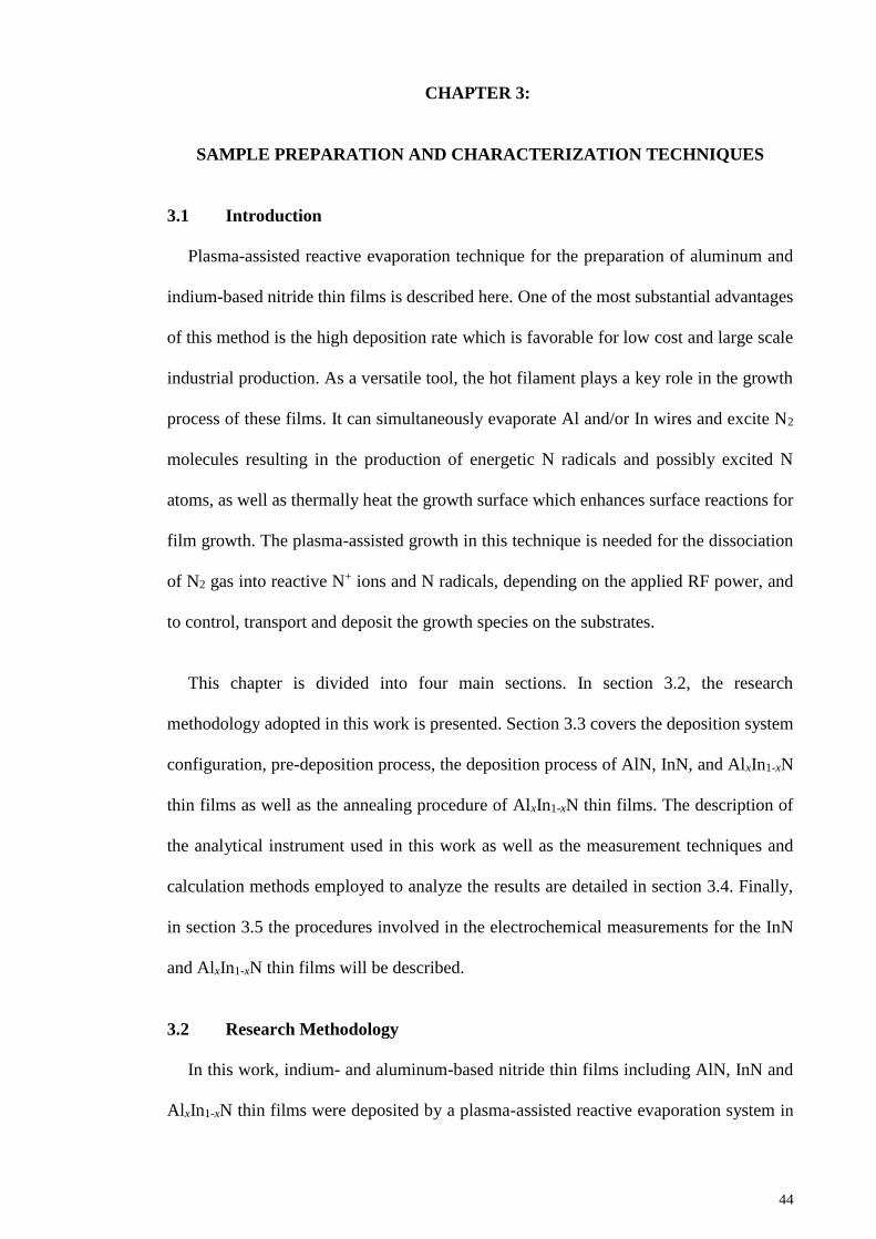
44
CHAPTER 3:
SAMPLE PREPARATION AND CHARACTERIZATION TECHNIQUES
3.1 Introduction
Plasma-assisted reactive evaporation technique for the preparation of aluminum and
indium-based nitride thin films is described here. One of the most substantial advantages
of this method is the high deposition rate which is favorable for low cost and large scale
industrial production. As a versatile tool, the hot filament plays a key role in the growth
process of these films. It can simultaneously evaporate Al and/or In wires and excite N2
molecules resulting in the production of energetic N radicals and possibly excited N
atoms, as well as thermally heat the growth surface which enhances surface reactions for
film growth. The plasma-assisted growth in this technique is needed for the dissociation
of N2 gas into reactive N+ ions and N radicals, depending on the applied RF power, and
to control, transport and deposit the growth species on the substrates.
This chapter is divided into four main sections. In section 3.2, the research
methodology adopted in this work is presented. Section 3.3 covers the deposition system
configuration, pre-deposition process, the deposition process of AlN, InN, and AlxIn1-xN
thin films as well as the annealing procedure of AlxIn1-xN thin films. The description of
the analytical instrument used in this work as well as the measurement techniques and
calculation methods employed to analyze the results are detailed in section 3.4. Finally,
in section 3.5 the procedures involved in the electrochemical measurements for the InN
and AlxIn1-xN thin films will be described.
3.2 Research Methodology
In this work, indium- and aluminum-based nitride thin films including AlN, InN and
AlxIn1-xN thin films were deposited by a plasma-assisted reactive evaporation system in
45
the Low Dimensional Materials Research Centre, Department of Physics, University of
Malaya. The aim was to introduce a cost-effective and environmental-friendly method for
deposition of indium and aluminum based nitride thin films at low temperatures. The
flowchart of the research methodology involved in this work is shown in Figure 3.1. This
project started with the growth of AlN thin films at various filament-substrate distances
followed by characterization of the grown films using different analytical tools. Next, the
deposition and characterization of InN thin films grown at various RF powers were carried
out. The results and discussions corresponding to the deposition of AlN and InN thin films
are presented in chapter 4. The electrochemical properties of InN thin films were also
investigated and are explained in detail in chapter 6.
The parameters used for the growth of AlN and InN were employed for the deposition
of AlxIn1-xN thin films, and the first set of AlxIn1-xN alloys was deposited at various AC
voltages applied to the filament holding the indium wire. The characterization of the
grown AlxIn1-xN thin films showed that Al-rich and In-rich AlxIn1-xN films can be obtained
by varying the voltage. In the next step, one sample of Al-rich and In-rich each were
selected and the effects of the nitrogen flow rate on the properties of the films were
investigated. An annealing study of the In-rich AlxIn1-xN films was performed at various
temperatures to examine the stability of the films for potential applications. All the results
of the above-mentioned steps on the growth of AlxIn1-xN films are presented and discussed
in chapter 5. Finally, the photoelectrochemical behavior of Al-rich AlxIn1-xN films for
potential water splitting applications was investigated and the obtained results are
presented and discussed in chapter 6.
46
Figure 3.1: Flowchart of research methodology involved in this work.
47
3.3 Deposition of the Thin Films
3.3.1 Deposition System
A home-built plasma-assisted reactive evaporation system was designed and set up for
the deposition of binary and trinary indium- and aluminum-based nitride thin films. An
actual photograph of the system is shown in Figure 3.2. The system mainly consisted of
four parts: evacuation system, electrical system, reaction chamber, and gas distribution
system as shown in Figure 3.2. The evacuation system included two parts, i.e., the rotary
and turbomolecular pumps. The turbomolecular pump was backed up with another rotary
pump as shown in Figure 3.2. The electrical system consisted of a RF power supply and
matching impendence, two hot wire supplies, and temperature controller. The reaction
chamber included a top plate, chamber body, and a base plate all of which were made of
stainless steel to withstand high temperatures and to provide good vacuum conditions
during the growth process.
A schematic diagram of the reaction chamber used for the growth of binary thin films
(e.g., AlN and InN) is shown in Figure 3.3. The top plate which has a diameter and
thickness of 31.5 and 0.8 cm, respectively, was attached to an air admittance valve, gas
inlet, the RF power supply connector, and the hot filament supply connectors. A Teflon
block was employed between the gas shower head and the gas inlet to isolate the gas
shower and for the establishment of plasma ambient; as such, the shower head also acted
as the powered electrode. The RF power was supplied by using an ENI power supply at
13.56 MHz. The hot filament supply connectors were attached to two cupper rods
connected to cupper holders which clamped a tungsten filament between the shower head
and the substrate holder inside the chamber body. The tungsten filament was used for
evaporation of Al/In wires and labeled as FAl/FIn. For the AlInN ternary thin films two
separate filaments were clamped perpendicularly to each other (see inset of Figure 3.4)
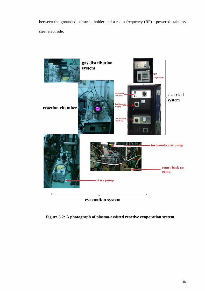
48
between the grounded substrate holder and a radio-frequency (RF) - powered stainless
steel electrode.
Figure 3.2: A photograph of plasma-assisted reactive evaporation system.
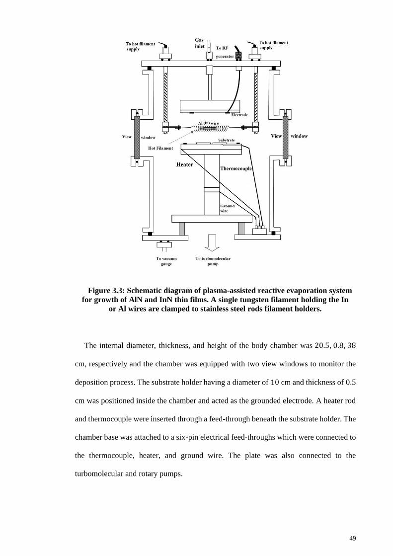
49
Figure 3.3: Schematic diagram of plasma-assisted reactive evaporation system
for growth of AlN and InN thin films. A single tungsten filament holding the In
or Al wires are clamped to stainless steel rods filament holders.
The internal diameter, thickness, and height of the body chamber was 20.5, 0.8, 38
cm, respectively and the chamber was equipped with two view windows to monitor the
deposition process. The substrate holder having a diameter of 10 cm and thickness of 0.5
cm was positioned inside the chamber and acted as the grounded electrode. A heater rod
and thermocouple were inserted through a feed-through beneath the substrate holder. The
chamber base was attached to a six-pin electrical feed-throughs which were connected to
the thermocouple, heater, and ground wire. The plate was also connected to the
turbomolecular and rotary pumps.
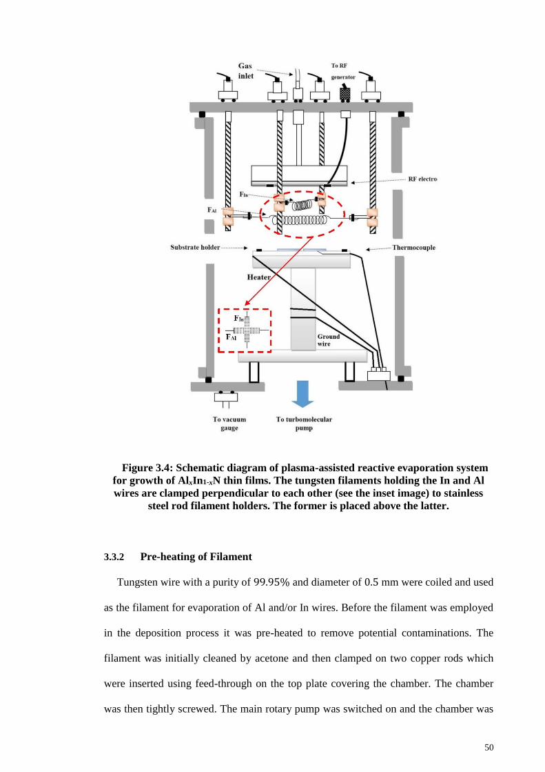
50
Figure 3.4: Schematic diagram of plasma-assisted reactive evaporation system
for growth of AlxIn1-xN thin films. The tungsten filaments holding the In and Al
wires are clamped perpendicular to each other (see the inset image) to stainless
steel rod filament holders. The former is placed above the latter.
3.3.2 Pre-heating of Filament
Tungsten wire with a purity of 99.95% and diameter of 0.5 mm were coiled and used
as the filament for evaporation of Al and/or In wires. Before the filament was employed
in the deposition process it was pre-heated to remove potential contaminations. The
filament was initially cleaned by acetone and then clamped on two copper rods which
were inserted using feed-through on the top plate covering the chamber. The chamber
was then tightly screwed. The main rotary pump was switched on and the chamber was
51
pumped down to a pressure of around 10−3 mbar. Then, hydrogen gas with a flow rate of
100 sccm was admitted into the chamber and the filament was heated to around 1800 °C
for 10 minutes. Finally, the filament power supply was switched off, the valves admitting
the gas were closed and the system cooled down for 2 hours under vacuum condition.
3.3.3 Preparation of Substrates
AlN, InN, and AlxIn1-xN thin films were deposited on silicon and quartz substrates.
625 µm-thick crystal silicon (c-Si) with (111) orientation and quartz glass having a
thickness of 1.0 mm were used for deposition of the films. The substrates were cleaved
into quadrangular-shaped pieces with dimension of 1.5 × 1.5 cm and cleaned thoroughly
before insertion into the chamber. Each quartz and silicon substrates was cleaned using
different procedures.
The Si (111) substrates were initially rinsed with deionized water to remove dust and
other particles from the surface and then immersed in H2O:H2O2:HCl (at 6: 1: 1 ratio)
solution for 5 minutes. Next, the substrates were again rinsed in deionized water for 5
minutes. This was repeated for H2O:H2O2:NH4OH (at 5: 1: 1 ratio) and with H2O:HF (at
10: 1 ratio) solutions to remove the oxide layer and other residue contaminants from the
surface (Goh, 2012). Finally, the substrates were dried by using compressed nitrogen.
The cleaning procedure for the quartz substrates was somewhat simpler than for the
silicon ones. First, they were ultrasonically degreased in decon 90 soap for 30 minutes,
then rinsed in deionized water, ethanol, and acetone, and subsequently dried using
nitrogen gas (Goh, 2012).
3.3.4 Pre-deposition Process
Prior to the deposition process the substrate holder, filament holder and shower head
were thoroughly cleaned by sandpaper to eliminate any contamination and then cleaned
52
with acetone. The chamber body was wiped with a soft tissue soaked in acetone. The
shower head was connected to the RF power supply and the substrate holder was attached
to the heater and the thermocouple. The cleaned substrates were placed directly on the
substrate holder and the tungsten filament was clamped to the stainless steel rod holders
inserted by feed-throughs from the top plate of the deposition chamber. The filament was
clamped between the substrates and the shower head. Al (In) wire was placed inside the
coils of the filament, the chamber was tightly screwed and all the valves of the system
were closed before the evacuation process was commenced.
The evacuation process was done in 3 steps. In the first step, the rotary pump was
switched on and the rotary valve slowly opened to its maximum. The pumping process
was continuously conducted until the vacuum pressure reached around 10−3 mbar. To
evacuate any residual gases inside the gas lines, the line valves were opened. Next, the
backup rotary pump was switched on and the corresponding valve was opened. This pump
acted as the backing for the turbomolecular pump. In the second step, the main rotary
pump was closed, the turbumolecular pump switched on for one hour and a minimum
pressure, called the base pressure, was obtained. Finally, the turbomolecular pump and
the backup rotary pump were switched off and the main rotary pump was opened.
To activate the surface bonds, H2-plasma treatment was performed on the surface of
the substrates for 10 min at a fixed hydrogen gas flow rate of 100 sccm using the mass
flow controller (MFC). The RF power during hydrogen treatment process was 15 W. It
has been shown that plasma treatment significantly improves the films adhesion on the
substrates (Ostrikov, 2005). Upon completion of the treatment the RF power supply was
switched off, the MFC was closed, and the residual H2 pumped out.
53
3.3.5 Deposition of AlN Thin Films
AlN thin films were deposited using a plasma-assisted single source reactive
evaporation system (Figure 3.3). The deposition process for the films was carried out in
2 steps. First, purified nitrogen gas (purity = 99.9999%) was admitted into the chamber
and plasma ambient was generated and stabilized for 5 minutes. Then, the tungsten
filament was heated to around 1650 °C and the deposition process was performed by
evaporating the Al wire under an N2 plasma environment. During the process the substrate
temperature (Ts) increased due to ion bombardment and radiant heat from the plasma and
the hot filament, respectively. No external heating was used during the deposition process.
However, due to ion bombardment from the plasma and radiant heat from the hot filament
the substrate temperature during the deposition process varied from 150 to 200 °C
depending on the distance between the filament and substrate. After the deposition
process the filament and the plasma supply were switched off and the system cooled down
under the flow of N2 gas until the temperature reached around 50 °C. The effect of the
filament-to-substrate distance on the structure, composition, and morphology of AlN thin
films was studied. The filament-to-substrate distance (𝑑𝑓−𝑠) was varied in 0.4 cm
increments from 1.0 to 2.2 cm and other parameters were fixed during the process. A list
of the parameter values for the growth of AlN thin films is summarized in Table 3.1.
3.3.6 Deposition of InN Thin Films
The plasma-assisted single source reactive evaporation system (Figure 3.3) was also
employed for growth of InN thin films. Prior to the actual deposition process the
substrates were externally heated to 200 °C. The deposition process for InN thin films
was carried out in 3 steps. First, purified nitrogen gas (purity = 99.9999%) was admitted
into the chamber and plasma ambient generated and stabilized for 5 minutes. Then, the
tungsten filament was heated to 1050 °C and the deposition process was performed by
evaporating the In wire under N2 plasma. During the process, the substrate temperature
54
(Ts) increased due to ion bombardment and radiant heat from the plasma and the hot
filament, respectively, and the substrate temperature reached around 350 °C. After the
deposition process and before switching off the system the sample was in situ annealed
under N2 plasma ambient (RF= 50 W) and hot filament (Tf = 950 °C) for 30 minutes.
The effect of RF power on crystallinity, composition, morphology and optical
properties of InN thin films was investigated. The RF power was changed in 50 W
increments from 50 to 250 W and other parameters were fixed during the process. A list
of the parameter values for growth of InN thin films is summarized in Table 3.1.
3.3.7 Deposition of AlxIn1-xN Thin Films
The AlxIn1-xN films were deposited on quartz and Si (111) substrates by the plasma-
assisted dual source reactive evaporation system (Figure 3.4). Two separate tungsten
wires were used as the hot filaments for evaporation of indium and aluminum wires. The
deposition process was conducted in three steps, as follows: 1) N2 plasma was generated
in the chamber and stabilized for 5 min, 2) FAl was heated to the temperature required for
evaporation of Al atoms (T𝑓~ 1650 °C) and then cooled to 1450 °C to avoid high
evaporation rates, and 3) an AC voltage was immediately applied to the FIn filament and
the AlxIn1-xN film formation was initiated. Conditions for the film growth were
maintained under N2 plasma for 5 min. The substrates were initially heated to 200 °C
and, during the deposition process, the final substrate holder temperature was varied from
320 to 360 °C (depending on the AC voltage applied to FIn (VIn)). After the deposition
process, the FIn was switched off and the FAl temperature was fixed at 1300 °C and the
obtained samples were annealed in N2 plasma (flow rate: 40 sccm, RF power: 50 W)
for 30 min.
Three sets of samples were deposited for the AlxIn1-xN thin films. In the first set, the
AC voltage applied to FAl (VAl) was set at 75 V, while that applied to FIn (VIn) was varied
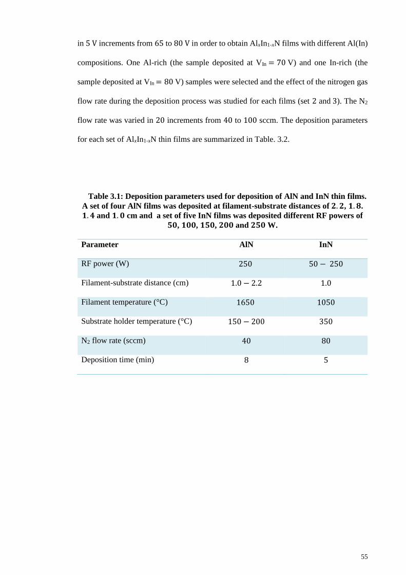
55
in 5 V increments from 65 to 80 V in order to obtain AlxIn1-xN films with different Al(In)
compositions. One Al-rich (the sample deposited at VIn = 70 V) and one In-rich (the
sample deposited at VIn = 80 V) samples were selected and the effect of the nitrogen gas
flow rate during the deposition process was studied for each films (set 2 and 3). The N2
flow rate was varied in 20 increments from 40 to 100 sccm. The deposition parameters
for each set of AlxIn1-xN thin films are summarized in Table. 3.2.
Table 3.1: Deposition parameters used for deposition of AlN and InN thin films.
A set of four AlN films was deposited at filament-substrate distances of 𝟐. 𝟐, 𝟏. 𝟖.
𝟏. 𝟒 and 𝟏. 𝟎 cm and a set of five InN films was deposited different RF powers of
𝟓𝟎, 𝟏𝟎𝟎, 𝟏𝟓𝟎, 𝟐𝟎𝟎 and 𝟐𝟓𝟎 W.
Parameter AlN InN
RF power (W) 250 50 − 250
Filament-substrate distance (cm) 1.0 − 2.2 1.0
Filament temperature (°C) 1650 1050
Substrate holder temperature (°C) 150 − 200 350
N2 flow rate (sccm) 40 80
Deposition time (min) 8 5
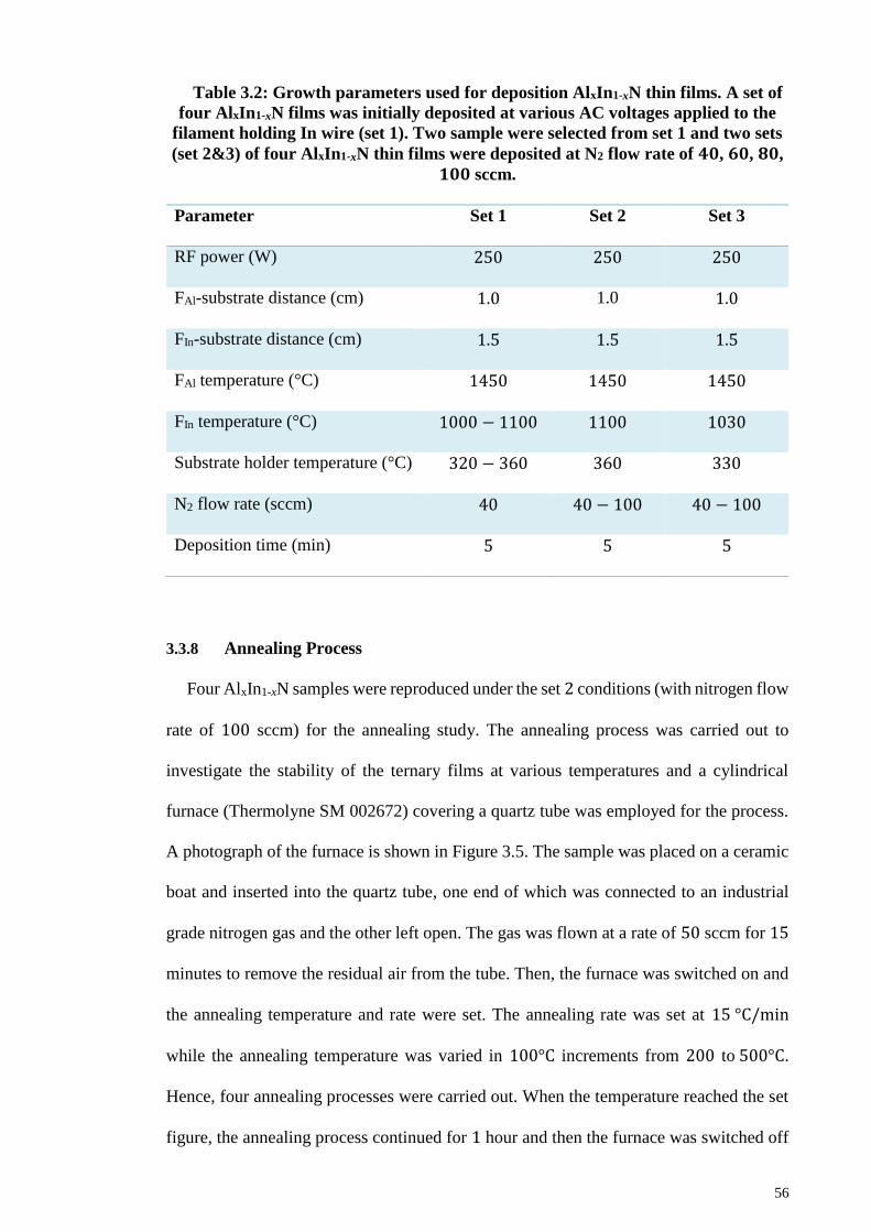
56
Table 3.2: Growth parameters used for deposition AlxIn1-xN thin films. A set of
four AlxIn1-xN films was initially deposited at various AC voltages applied to the
filament holding In wire (set 1). Two sample were selected from set 1 and two sets
(set 2&3) of four AlxIn1-xN thin films were deposited at N2 flow rate of 𝟒𝟎, 𝟔𝟎, 𝟖𝟎,
𝟏𝟎𝟎 sccm.
Parameter Set 1 Set 2 Set 3
RF power (W) 250 250 250
FAl-substrate distance (cm) 1.0 1.0 1.0
FIn-substrate distance (cm) 1.5 1.5 1.5
FAl temperature (°C) 1450 1450 1450
FIn temperature (°C) 1000 − 1100 1100 1030
Substrate holder temperature (°C) 320 − 360 360 330
N2 flow rate (sccm) 40 40 − 100 40 − 100
Deposition time (min) 5 5 5
3.3.8 Annealing Process
Four AlxIn1-xN samples were reproduced under the set 2 conditions (with nitrogen flow
rate of 100 sccm) for the annealing study. The annealing process was carried out to
investigate the stability of the ternary films at various temperatures and a cylindrical
furnace (Thermolyne SM 002672) covering a quartz tube was employed for the process.
A photograph of the furnace is shown in Figure 3.5. The sample was placed on a ceramic
boat and inserted into the quartz tube, one end of which was connected to an industrial
grade nitrogen gas and the other left open. The gas was flown at a rate of 50 sccm for 15
minutes to remove the residual air from the tube. Then, the furnace was switched on and
the annealing temperature and rate were set. The annealing rate was set at 15 °C/min
while the annealing temperature was varied in 100°C increments from 200 to 500°C.
Hence, four annealing processes were carried out. When the temperature reached the set
figure, the annealing process continued for 1 hour and then the furnace was switched off
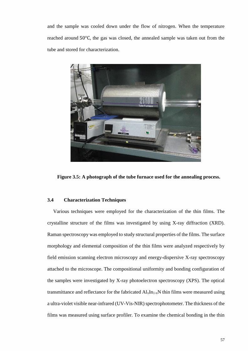
57
and the sample was cooled down under the flow of nitrogen. When the temperature
reached around 50°C, the gas was closed, the annealed sample was taken out from the
tube and stored for characterization.
Figure 3.5: A photograph of the tube furnace used for the annealing process.
3.4 Characterization Techniques
Various techniques were employed for the characterization of the thin films. The
crystalline structure of the films was investigated by using X-ray diffraction (XRD).
Raman spectroscopy was employed to study structural properties of the films. The surface
morphology and elemental composition of the thin films were analyzed respectively by
field emission scanning electron microscopy and energy-dispersive X-ray spectroscopy
attached to the microscope. The compositional uniformity and bonding configuration of
the samples were investigated by X-ray photoelectron spectroscopy (XPS). The optical
transmittance and reflectance for the fabricated AlxIn1-xN thin films were measured using
a ultra-violet visible near-infrared (UV-Vis-NIR) spectrophotometer. The thickness of the
films was measured using surface profiler. To examine the chemical bonding in the thin
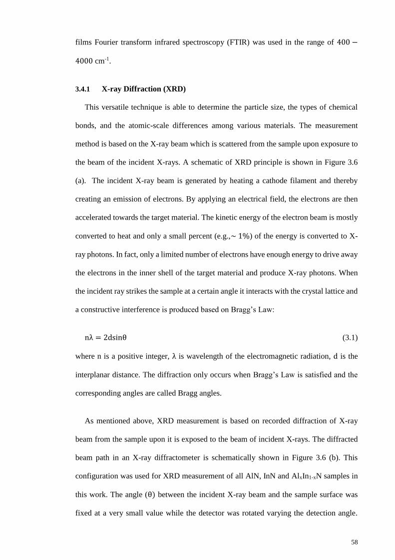
58
films Fourier transform infrared spectroscopy (FTIR) was used in the range of 400 −
4000 cm-1.
3.4.1 X-ray Diffraction (XRD)
This versatile technique is able to determine the particle size, the types of chemical
bonds, and the atomic-scale differences among various materials. The measurement
method is based on the X-ray beam which is scattered from the sample upon exposure to
the beam of the incident X-rays. A schematic of XRD principle is shown in Figure 3.6
(a). The incident X-ray beam is generated by heating a cathode filament and thereby
creating an emission of electrons. By applying an electrical field, the electrons are then
accelerated towards the target material. The kinetic energy of the electron beam is mostly
converted to heat and only a small percent (e.g.,~ 1%) of the energy is converted to X-
ray photons. In fact, only a limited number of electrons have enough energy to drive away
the electrons in the inner shell of the target material and produce X-ray photons. When
the incident ray strikes the sample at a certain angle it interacts with the crystal lattice and
a constructive interference is produced based on Bragg’s Law:
nλ = 2dsinθ (3.1)
where n is a positive integer, λ is wavelength of the electromagnetic radiation, d is the
interplanar distance. The diffraction only occurs when Bragg’s Law is satisfied and the
corresponding angles are called Bragg angles.
As mentioned above, XRD measurement is based on recorded diffraction of X-ray
beam from the sample upon it is exposed to the beam of incident X-rays. The diffracted
beam path in an X-ray diffractometer is schematically shown in Figure 3.6 (b). This
configuration was used for XRD measurement of all AlN, InN and AlxIn1-xN samples in
this work. The angle (θ) between the incident X-ray beam and the sample surface was
fixed at a very small value while the detector was rotated varying the detection angle.
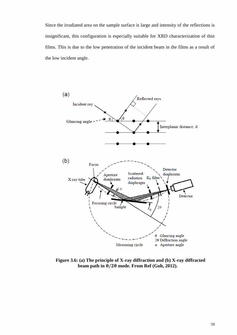
59
Since the irradiated area on the sample surface is large and intensity of the reflections is
insignificant, this configuration is especially suitable for XRD characterization of thin
films. This is due to the low penetration of the incident beam in the films as a result of
the low incident angle.
Figure 3.6: (a) The principle of X-ray diffraction and (b) X-ray diffracted
beam path in 𝛉/𝟐𝛉 mode. From Ref (Goh, 2012).
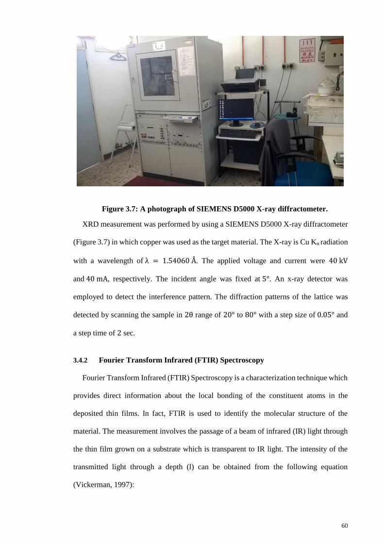
60
Figure 3.7: A photograph of SIEMENS D5000 X-ray diffractometer.
XRD measurement was performed by using a SIEMENS D5000 X-ray diffractometer
(Figure 3.7) in which copper was used as the target material. The X-ray is Cu Kα radiation
with a wavelength of λ = 1.54060 Å. The applied voltage and current were 40 kV
and 40 mA, respectively. The incident angle was fixed at 5°. An x-ray detector was
employed to detect the interference pattern. The diffraction patterns of the lattice was
detected by scanning the sample in 2θ range of 20° to 80° with a step size of 0.05° and
a step time of 2 sec.
3.4.2 Fourier Transform Infrared (FTIR) Spectroscopy
Fourier Transform Infrared (FTIR) Spectroscopy is a characterization technique which
provides direct information about the local bonding of the constituent atoms in the
deposited thin films. In fact, FTIR is used to identify the molecular structure of the
material. The measurement involves the passage of a beam of infrared (IR) light through
the thin film grown on a substrate which is transparent to IR light. The intensity of the
transmitted light through a depth (l) can be obtained from the following equation
(Vickerman, 1997):
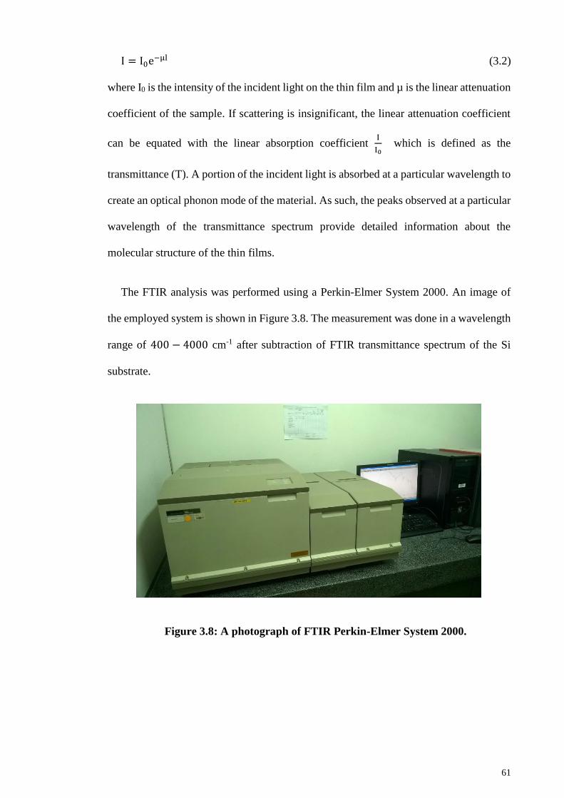
61
I = I0e−µl (3.2)
where I0 is the intensity of the incident light on the thin film and µ is the linear attenuation
coefficient of the sample. If scattering is insignificant, the linear attenuation coefficient
can be equated with the linear absorption coefficient I
I0 which is defined as the
transmittance (T). A portion of the incident light is absorbed at a particular wavelength to
create an optical phonon mode of the material. As such, the peaks observed at a particular
wavelength of the transmittance spectrum provide detailed information about the
molecular structure of the thin films.
The FTIR analysis was performed using a Perkin-Elmer System 2000. An image of
the employed system is shown in Figure 3.8. The measurement was done in a wavelength
range of 400 − 4000 cm-1 after subtraction of FTIR transmittance spectrum of the Si
substrate.
Figure 3.8: A photograph of FTIR Perkin-Elmer System 2000.
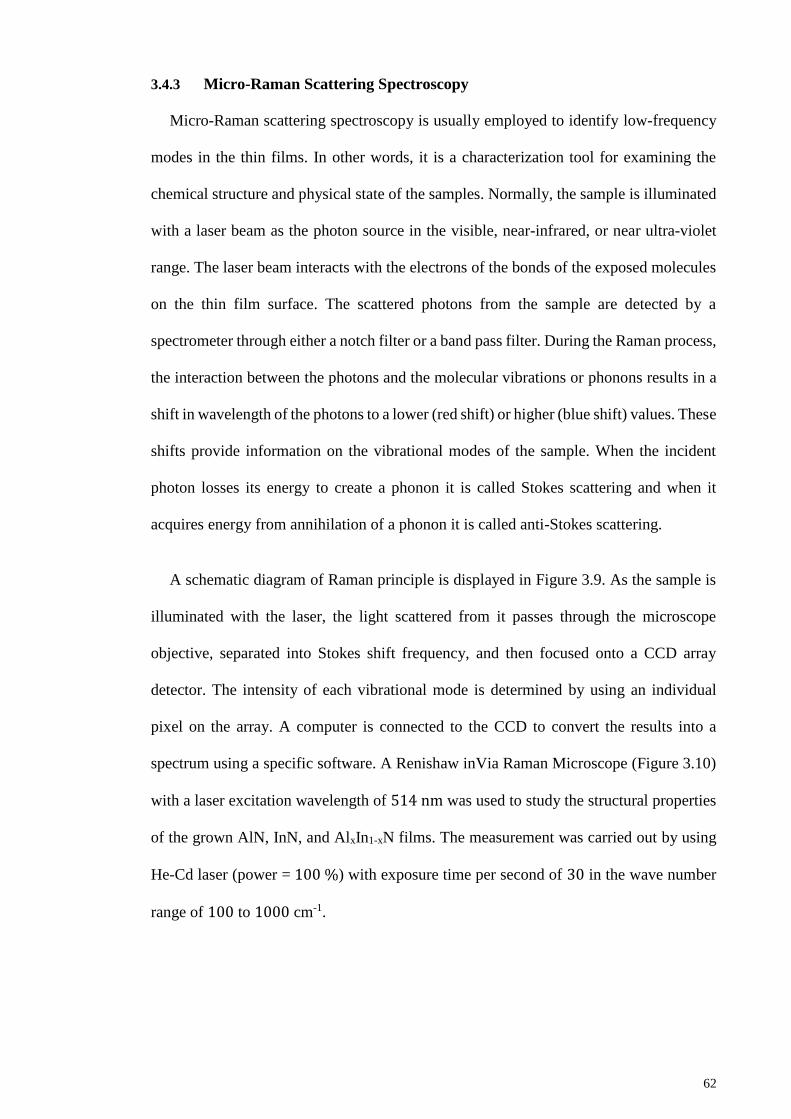
62
3.4.3 Micro-Raman Scattering Spectroscopy
Micro-Raman scattering spectroscopy is usually employed to identify low-frequency
modes in the thin films. In other words, it is a characterization tool for examining the
chemical structure and physical state of the samples. Normally, the sample is illuminated
with a laser beam as the photon source in the visible, near-infrared, or near ultra-violet
range. The laser beam interacts with the electrons of the bonds of the exposed molecules
on the thin film surface. The scattered photons from the sample are detected by a
spectrometer through either a notch filter or a band pass filter. During the Raman process,
the interaction between the photons and the molecular vibrations or phonons results in a
shift in wavelength of the photons to a lower (red shift) or higher (blue shift) values. These
shifts provide information on the vibrational modes of the sample. When the incident
photon losses its energy to create a phonon it is called Stokes scattering and when it
acquires energy from annihilation of a phonon it is called anti-Stokes scattering.
A schematic diagram of Raman principle is displayed in Figure 3.9. As the sample is
illuminated with the laser, the light scattered from it passes through the microscope
objective, separated into Stokes shift frequency, and then focused onto a CCD array
detector. The intensity of each vibrational mode is determined by using an individual
pixel on the array. A computer is connected to the CCD to convert the results into a
spectrum using a specific software. A Renishaw inVia Raman Microscope (Figure 3.10)
with a laser excitation wavelength of 514 nm was used to study the structural properties
of the grown AlN, InN, and AlxIn1-xN films. The measurement was carried out by using
He-Cd laser (power = 100 %) with exposure time per second of 30 in the wave number
range of 100 to 1000 cm-1.
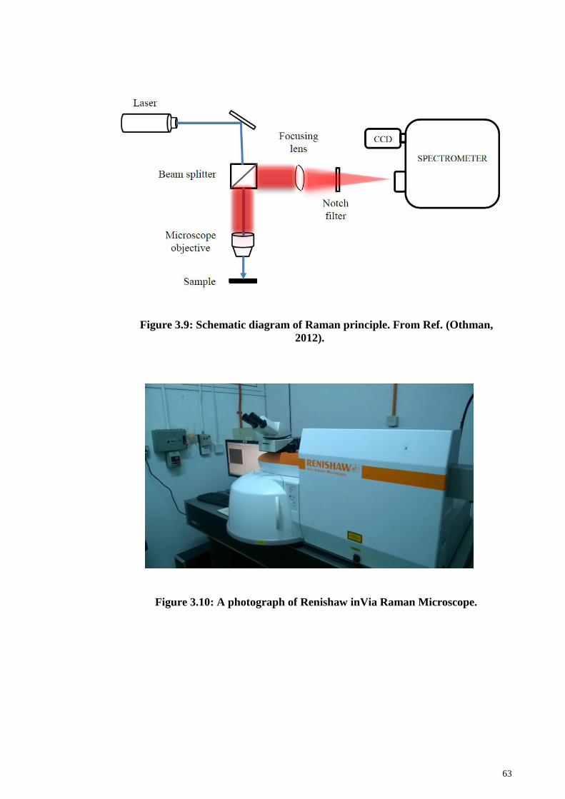
63
Figure 3.9: Schematic diagram of Raman principle. From Ref. (Othman,
2012).
Figure 3.10: A photograph of Renishaw inVia Raman Microscope.
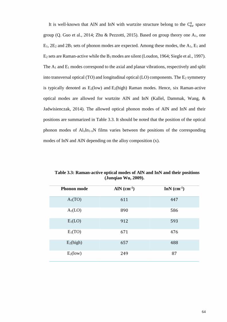
64
It is well-known that AlN and InN with wurtzite structure belong to the C6v4 space
group (Q. Guo et al., 2014; Zhu & Pezzotti, 2015). Based on group theory one A1, one
E1, 2E2 and 2B1 sets of phonon modes are expected. Among these modes, the A1, E1 and
E2 sets are Raman-active while the B1 modes are silent (Loudon, 1964; Siegle et al., 1997).
The A1 and E1 modes correspond to the axial and planar vibrations, respectively and split
into transversal optical (TO) and longitudinal optical (LO) components. The E2 symmetry
is typically denoted as E2(low) and E2(high) Raman modes. Hence, six Raman-active
optical modes are allowed for wurtzite AlN and InN (Kallel, Dammak, Wang, &
Jadwisienczak, 2014). The allowed optical phonon modes of AlN and InN and their
positions are summarized in Table 3.3. It should be noted that the position of the optical
phonon modes of AlxIn1-xN films varies between the positions of the corresponding
modes of InN and AlN depending on the alloy composition (x).
Table 3.3: Raman-active optical modes of AlN and InN and their positions
(Junqiao Wu, 2009).
Phonon mode AlN (cm-1) InN (cm-1)
A1(TO) 611 447
A1(LO) 890 586
E1(LO) 912 593
E1(TO) 671 476
E2(high) 657 488
E2(low) 249 87
65
3.4.4 Field Emission Scanning Electron Microscopy (FESEM) and Energy-
Dispersive X-ray (EDX) Spectroscopy
Field emission scanning electron microscopy was employed to observe the
topographical details on the surface of the thin films at magnifications of 10x to
300,000x. In the microscope a field emission source is used to liberate the electrons in a
high electrical field gradient which gives rise to the electrons gaining high energy when
they travel within the high vacuum column. The energetic electrons (so-called primary
electrons) are then condensed by electronic lenses to provide bombardment of the thin
films with a narrow scan beam. As a result, secondary electrons are ejected from the
surface of the thin films. A detector is used to catch the secondary electrons and to
produce electronic signals which are then transduced to a video scan to produce
morphology images. Resolution of the images strongly depends on accumulation of the
secondary electrons.
Energy-dispersive X-ray spectroscopy (EDX) is an analytical characterization
technique that commonly used for elemental composition of a sample. This technique is
based on the interaction between a high-energy beam of electrons or a beam of X-rays
and a sample. The incident beam is able to excite the inner shell electrons (lower energy
shells) and dislodge them from the shell resulting in the formation of electron holes in the
shells. The electrons from the outer shells (higher-energy shells) recombine the holes and
release energy in form of X-rays. The released energy which is equal to the difference
between the energies of the outer and inner shells, is the characteristic of the atomic
structure of the emitting element and appears as a peak in the EDX spectrum.
Surface morphology of the InN and AlxIn1-xN thin films were analyzed by JEOL JSM-
7600F microscope. The elemental composition of the films were measured by X-Max
Oxford Instruments EDX attached to the microscope. A picture of the machine is shown
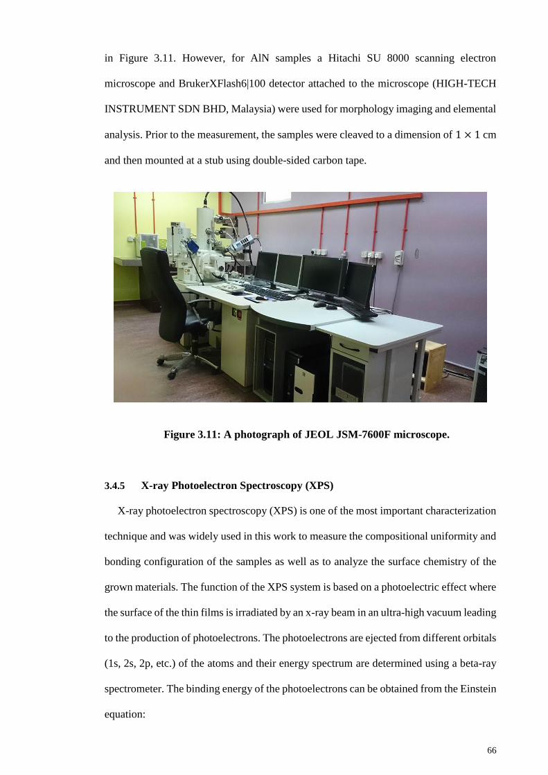
66
in Figure 3.11. However, for AlN samples a Hitachi SU 8000 scanning electron
microscope and BrukerXFlash6|100 detector attached to the microscope (HIGH-TECH
INSTRUMENT SDN BHD, Malaysia) were used for morphology imaging and elemental
analysis. Prior to the measurement, the samples were cleaved to a dimension of 1 × 1 cm
and then mounted at a stub using double-sided carbon tape.
Figure 3.11: A photograph of JEOL JSM-7600F microscope.
3.4.5 X-ray Photoelectron Spectroscopy (XPS)
X-ray photoelectron spectroscopy (XPS) is one of the most important characterization
technique and was widely used in this work to measure the compositional uniformity and
bonding configuration of the samples as well as to analyze the surface chemistry of the
grown materials. The function of the XPS system is based on a photoelectric effect where
the surface of the thin films is irradiated by an x-ray beam in an ultra-high vacuum leading
to the production of photoelectrons. The photoelectrons are ejected from different orbitals
(1s, 2s, 2p, etc.) of the atoms and their energy spectrum are determined using a beta-ray
spectrometer. The binding energy of the photoelectrons can be obtained from the Einstein
equation:
67
EBE = hν − EKE − φ (3.3)
where EBE is binding energy of the photoelectrons, hν is energy of the incident photons,
EKE is kinetic energy of the photoelectrons measured by the spectrometer and φ is work
function dependent on both the spectrometer and the material. Since the binding energies
of the electron orbitals in atoms are known, the atomic composition of the sample surface
is identified from the positions of the peaks in the XPS spectrum. Analyzing the
photoelectron peaks using the curve-fitting method allows us to quantitatively determine
the composition of the sample.
Three different systems including Shimadzu, Kratos Axis Ultra DLD (Institute of
Microengineering and Nanoelectronics (IMEN), Universiti Kebangsaan Malaysia,
Malaysia), PHI Quantera II (MIMOS national R&D center, Malaysia) and Thermo VG
Scientific, CLAM2 (the Synchrotron Light Research Institute, Thailand) were employed
for the XPS characterization of the AlxIn1-xN thin films. An image of the PHI Quantera II
system is shown in Figure 3.12. Since each system has specific calibrations and
parameters, all samples of a set were measured by using a single system. For instance, in
PHI Quantera II system a monochromatic Al K-alpha (1486.6 eV) at 25 W (15 kV and
3 mA) was used which was incident at 90° to the sample surface under base pressure
of 2 × 10⁻⁷ Pa. The obtained photoelectrons were collected at a take-off angle of 45°.
Narrow high-resolution scans of Al2p, In3d5/2, and N1s photoelectron spectra were run
with 0.1 eV steps and 20 ms dwell time. Scans were taken at analyzer pass energy of 112
eV. After measurement all the obtained peaks were calibrated by using the position of
C1s peak which is 284.6 eV. Then, A2p, In3d5/2, and N1s as the main elements of the
AlxIn1-xN thin films were analyzed to identify the bonding configuration of the alloys.
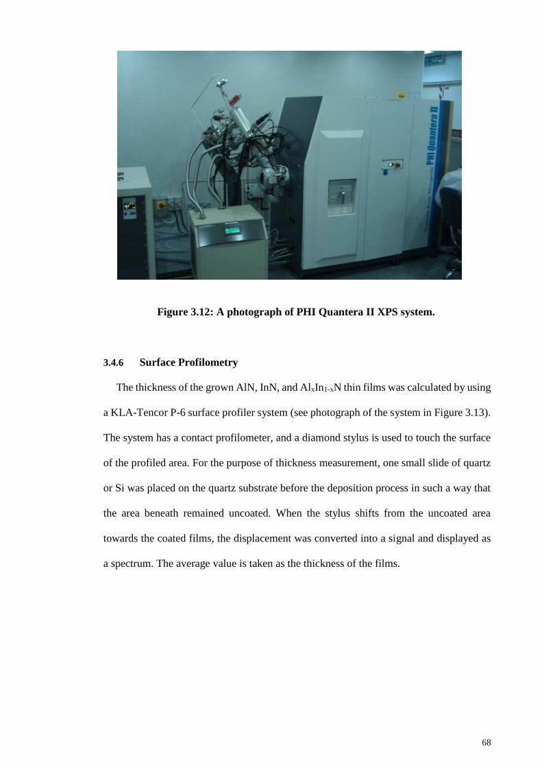
68
Figure 3.12: A photograph of PHI Quantera II XPS system.
3.4.6 Surface Profilometry
The thickness of the grown AlN, InN, and AlxIn1-xN thin films was calculated by using
a KLA-Tencor P-6 surface profiler system (see photograph of the system in Figure 3.13).
The system has a contact profilometer, and a diamond stylus is used to touch the surface
of the profiled area. For the purpose of thickness measurement, one small slide of quartz
or Si was placed on the quartz substrate before the deposition process in such a way that
the area beneath remained uncoated. When the stylus shifts from the uncoated area
towards the coated films, the displacement was converted into a signal and displayed as
a spectrum. The average value is taken as the thickness of the films.
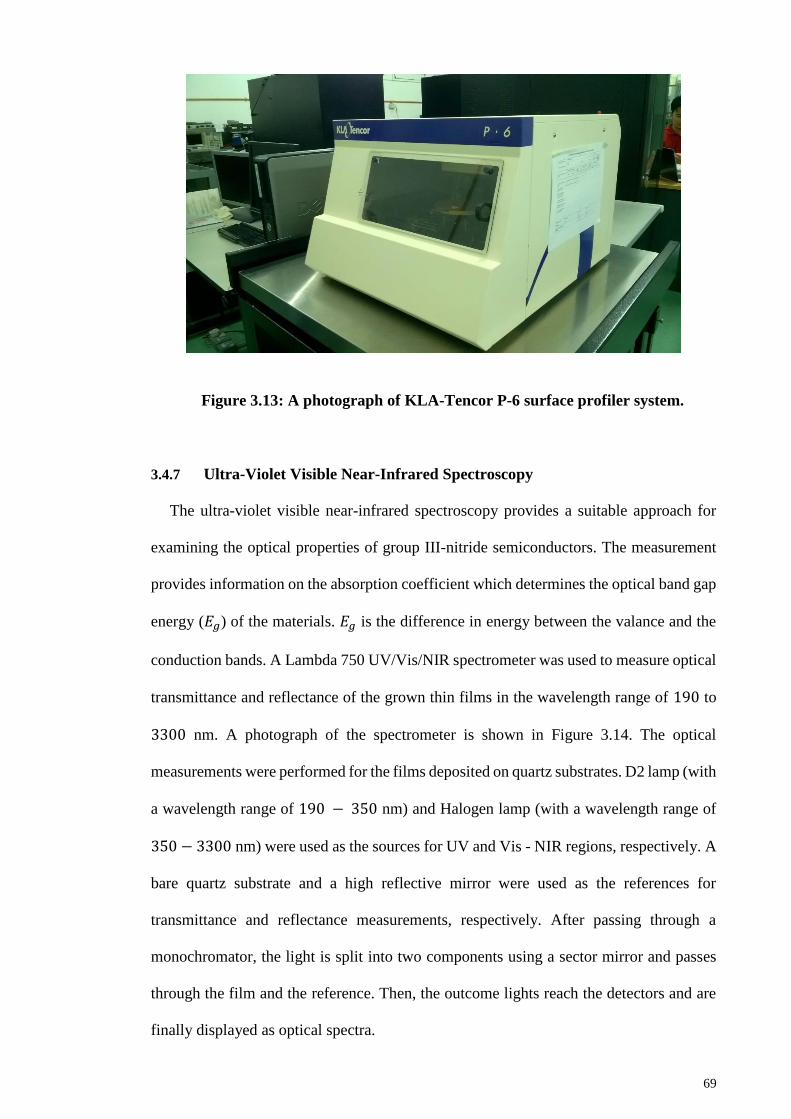
69
Figure 3.13: A photograph of KLA-Tencor P-6 surface profiler system.
3.4.7 Ultra-Violet Visible Near-Infrared Spectroscopy
The ultra-violet visible near-infrared spectroscopy provides a suitable approach for
examining the optical properties of group III-nitride semiconductors. The measurement
provides information on the absorption coefficient which determines the optical band gap
energy (𝐸𝑔) of the materials. 𝐸𝑔 is the difference in energy between the valance and the
conduction bands. A Lambda 750 UV/Vis/NIR spectrometer was used to measure optical
transmittance and reflectance of the grown thin films in the wavelength range of 190 to
3300 nm. A photograph of the spectrometer is shown in Figure 3.14. The optical
measurements were performed for the films deposited on quartz substrates. D2 lamp (with
a wavelength range of 190 − 350 nm) and Halogen lamp (with a wavelength range of
350 − 3300 nm) were used as the sources for UV and Vis - NIR regions, respectively. A
bare quartz substrate and a high reflective mirror were used as the references for
transmittance and reflectance measurements, respectively. After passing through a
monochromator, the light is split into two components using a sector mirror and passes
through the film and the reference. Then, the outcome lights reach the detectors and are
finally displayed as optical spectra.
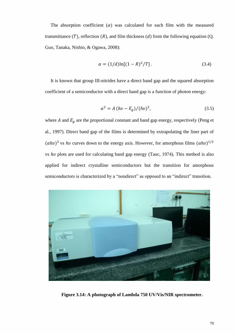
70
The absorption coefficient (𝛼) was calculated for each film with the measured
transmittance (𝑇), reflection (𝑅), and film thickness (𝑑) from the following equation (Q.
Guo, Tanaka, Nishio, & Ogawa, 2008):
𝛼 = (1/𝑑)ln[(1 − 𝑅)2 𝑇] ⁄ . (3.4)
It is known that group III-nitrides have a direct band gap and the squared absorption
coefficient of a semiconductor with a direct band gap is a function of photon energy:
𝛼2 = 𝐴 (ℎ𝜐 − 𝐸𝑔) (ℎ𝜐)2⁄ , (3.5)
where 𝐴 and 𝐸𝑔 are the proportional constant and band gap energy, respectively (Peng et
al., 1997). Direct band gap of the films is determined by extrapolating the liner part of
(𝛼ℎ𝜐)2 vs ℎ𝜐 curves down to the energy axis. However, for amorphous films (𝛼ℎ𝜐)1/2
vs ℎ𝜐 plots are used for calculating band gap energy (Tauc, 1974). This method is also
applied for indirect crystalline semiconductors but the transition for amorphous
semiconductors is characterized by a “nondirect” as opposed to an “indirect” transition.
Figure 3.14: A photograph of Lambda 750 UV/Vis/NIR spectrometer.
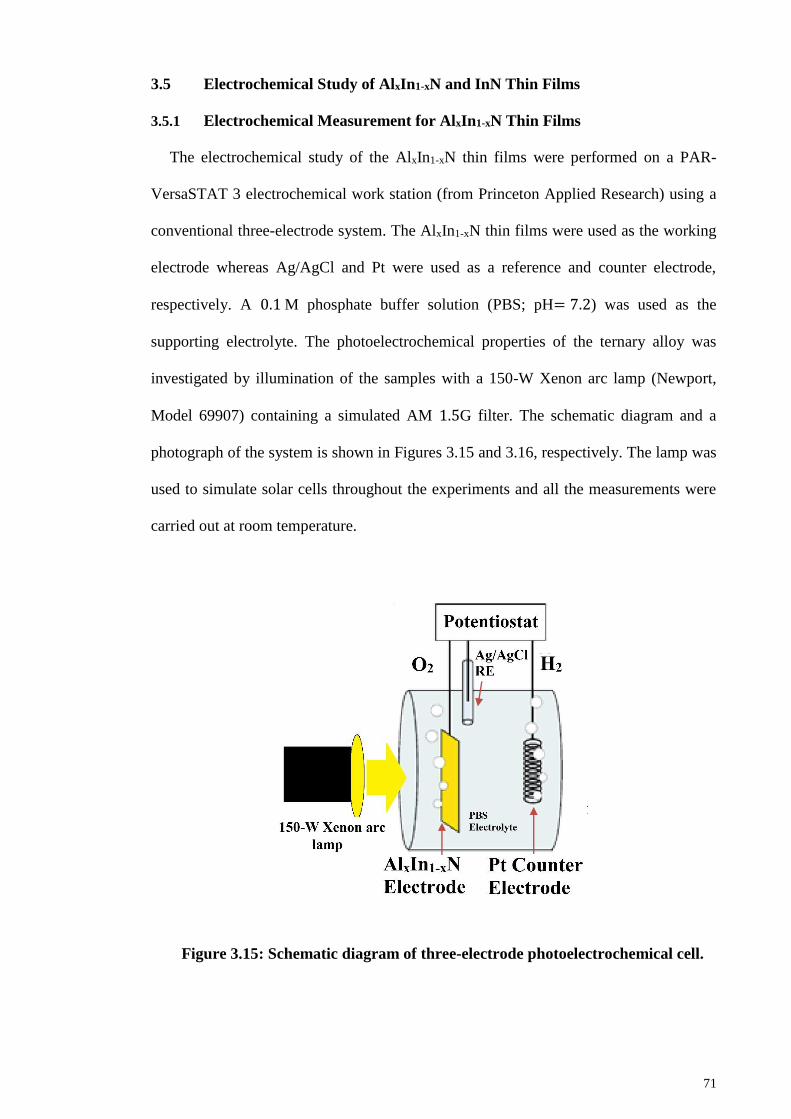
71
3.5 Electrochemical Study of AlxIn1-xN and InN Thin Films
3.5.1 Electrochemical Measurement for AlxIn1-xN Thin Films
The electrochemical study of the AlxIn1-xN thin films were performed on a PAR-
VersaSTAT 3 electrochemical work station (from Princeton Applied Research) using a
conventional three-electrode system. The AlxIn1-xN thin films were used as the working
electrode whereas Ag/AgCl and Pt were used as a reference and counter electrode,
respectively. A 0.1 M phosphate buffer solution (PBS; pH= 7.2) was used as the
supporting electrolyte. The photoelectrochemical properties of the ternary alloy was
investigated by illumination of the samples with a 150-W Xenon arc lamp (Newport,
Model 69907) containing a simulated AM 1.5G filter. The schematic diagram and a
photograph of the system is shown in Figures 3.15 and 3.16, respectively. The lamp was
used to simulate solar cells throughout the experiments and all the measurements were
carried out at room temperature.
Figure 3.15: Schematic diagram of three-electrode photoelectrochemical cell.
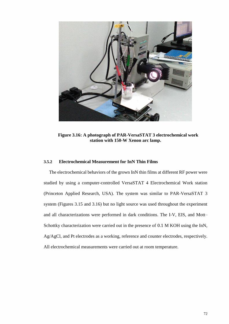
72
Figure 3.16: A photograph of PAR-VersaSTAT 3 electrochemical work
station with 150-W Xenon arc lamp.
3.5.2 Electrochemical Measurement for InN Thin Films
The electrochemical behaviors of the grown InN thin films at different RF power were
studied by using a computer-controlled VersaSTAT 4 Electrochemical Work station
(Princeton Applied Research, USA). The system was similar to PAR-VersaSTAT 3
system (Figures 3.15 and 3.16) but no light source was used throughout the experiment
and all characterizations were performed in dark conditions. The I-V, EIS, and Mott–
Schottky characterization were carried out in the presence of 0.1 M KOH using the InN,
Ag/AgCl, and Pt electrodes as a working, reference and counter electrodes, respectively.
All electrochemical measurements were carried out at room temperature.
73
CHAPTER 4:
ALUMINUM NITRIDE AND INDIUM NITRIDE THIN FILMS BY PLASMA-
ASSISTED REACTIVE EVAPORATION
4.1 Introduction
This chapter discusses two major studies on the effects of key deposition parameters
on the properties of aluminum nitride (AlN) and indium nitride (InN) thin films using the
plasma-assisted reactive evaporation technique. The first part of the chapter focuses on
the synthesis of AlN thin films at different filament-to-substrate distances (𝑑𝑓−𝑠) on Si
(111) substrates, where after the structural, compositional, and morphological properties
of the grown films will be compared. The structural and bonding characteristics of these
films were determined from the XRD and FTIR analysis. The surface morphology and
elemental composition of the thin films were analyzed respectively by FESEM and EDX
attached to the microscope.
The second part of this chapter studies the effects of plasma radio frequency (RF)
power on the properties of InN thin films deposited on Si (111) substrates. The objective
is to investigate how the crystallinity, composition, and band gap energy of InN thin films
are affected by RF power. The mechanism of changes in the films’ properties will be
discussed in detail.
4.2 Effects of Filament-to-Substrate Distance on the Structure, Morphology and
Optical Properties of Aluminum Nitride Thin Films
Figure 4.1 shows the XRD patterns of AlN thin films deposited at different filament-
substrate distances (𝑑𝑓−𝑠). The XRD pattern of the films grown at 𝑑𝑓−𝑠 = 2.2 cm exhibits
four sharp peaks at 2θ = 38.45°, 44.70°, 65.05° and 78.20°, which correspond to the
diffraction from the metallic Al (111), (200), (220) and (311) planes. One minor peak is
74
also observed at 2θ of 43.40° which is assigned to (004) plane of tungsten oxide (WO3).
Furthermore, two minor peaks are detected at 2θ = 33.35° and 35.85° which represents
the diffraction from the AlN (100) and (002) planes. These two peaks are indexed based
on an AlN hexagonal wurtzite-type structure. The metallic planes shrink significantly
when the distance is reduced to 1.8 and 1.4 cm and further decreasing 𝑑𝑓−𝑠 to 1.0 cm here
increased the intensity of the peaks corresponding to the AlN planes. This can be
explained by considering crystallography aspect of view. Due to enhanced radiant heat of
the filament on the growth surface and less probability of gas-phase reactions, shorter
filament-to-substrate distance provides the energy required for formation of AlN plains
which is much larger than the metallic ones. As a result, more Al and N adatoms are
bonded and form AlN crystalline planes.
In addition to AlN (100) and (002) planes, two more diffraction peaks, centered at
2θ of 37.55°, 59.10° and 71°, are observed from the XRD pattern of AlN films
deposited at 𝑑𝑓−𝑠 of 1.0 cm, which are assigned to the AlN (101), (110) and (200) planes.
The peak corresponded to AlN (200) is hardly observed possibly due the high energy
required for formation of this plane (L. Guo et al., 2016). Besides, the pattern suggests
that the AlN films grown at the shortest filament-substrate distances are preferentially
(002) oriented. At the shorter distance, higher surface mobility is imparted to the adatoms.
As mentioned in section 2.2, the energy required for growth particles to be deposited in
the planes of (002), (101) and (103) are relatively larger than that needed for (100). Hence,
the deposition of AlN thin films under shorter 𝑑𝑓−𝑠 is preferable for the orientation along
<002> direction. The significant decrease in intensity of metallic peaks along with the
preferential AlN growth orientation along the c-axis perpendicular to the substrate is
evidence of the constructive role of the short filament-to-substrate distance in improving
the crystallinity and quality of AlN.
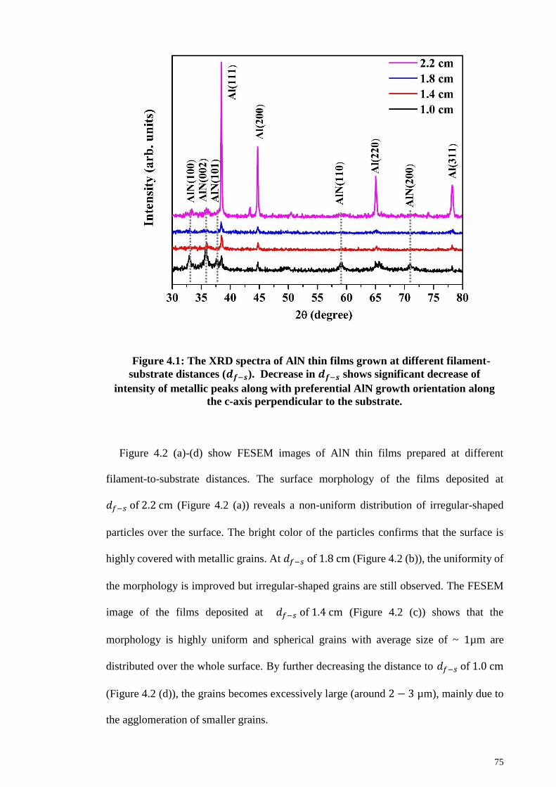
75
Figure 4.1: The XRD spectra of AlN thin films grown at different filament-
substrate distances (𝒅𝒇−𝒔). Decrease in 𝒅𝒇−𝒔 shows significant decrease of
intensity of metallic peaks along with preferential AlN growth orientation along
the c-axis perpendicular to the substrate.
Figure 4.2 (a)-(d) show FESEM images of AlN thin films prepared at different
filament-to-substrate distances. The surface morphology of the films deposited at
𝑑𝑓−𝑠 of 2.2 cm (Figure 4.2 (a)) reveals a non-uniform distribution of irregular-shaped
particles over the surface. The bright color of the particles confirms that the surface is
highly covered with metallic grains. At 𝑑𝑓−𝑠 of 1.8 cm (Figure 4.2 (b)), the uniformity of
the morphology is improved but irregular-shaped grains are still observed. The FESEM
image of the films deposited at 𝑑𝑓−𝑠 of 1.4 cm (Figure 4.2 (c)) shows that the
morphology is highly uniform and spherical grains with average size of ~ 1µm are
distributed over the whole surface. By further decreasing the distance to 𝑑𝑓−𝑠 of 1.0 cm
(Figure 4.2 (d)), the grains becomes excessively large (around 2 − 3 µm), mainly due to
the agglomeration of smaller grains.
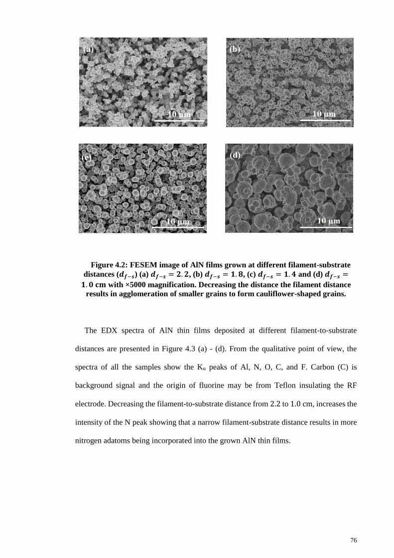
76
Figure 4.2: FESEM image of AlN films grown at different filament-substrate
distances (𝒅𝒇−𝒔) (a) 𝒅𝒇−𝒔 = 𝟐. 𝟐, (b) 𝒅𝒇−𝒔 = 𝟏. 𝟖, (c) 𝒅𝒇−𝒔 = 𝟏. 𝟒 and (d) 𝒅𝒇−𝒔 =
𝟏. 𝟎 𝐜𝐦 with ×5000 magnification. Decreasing the distance the filament distance
results in agglomeration of smaller grains to form cauliflower-shaped grains.
The EDX spectra of AlN thin films deposited at different filament-to-substrate
distances are presented in Figure 4.3 (a) - (d). From the qualitative point of view, the
spectra of all the samples show the Kα peaks of Al, N, O, C, and F. Carbon (C) is
background signal and the origin of fluorine may be from Teflon insulating the RF
electrode. Decreasing the filament-to-substrate distance from 2.2 to 1.0 cm, increases the
intensity of the N peak showing that a narrow filament-substrate distance results in more
nitrogen adatoms being incorporated into the grown AlN thin films.
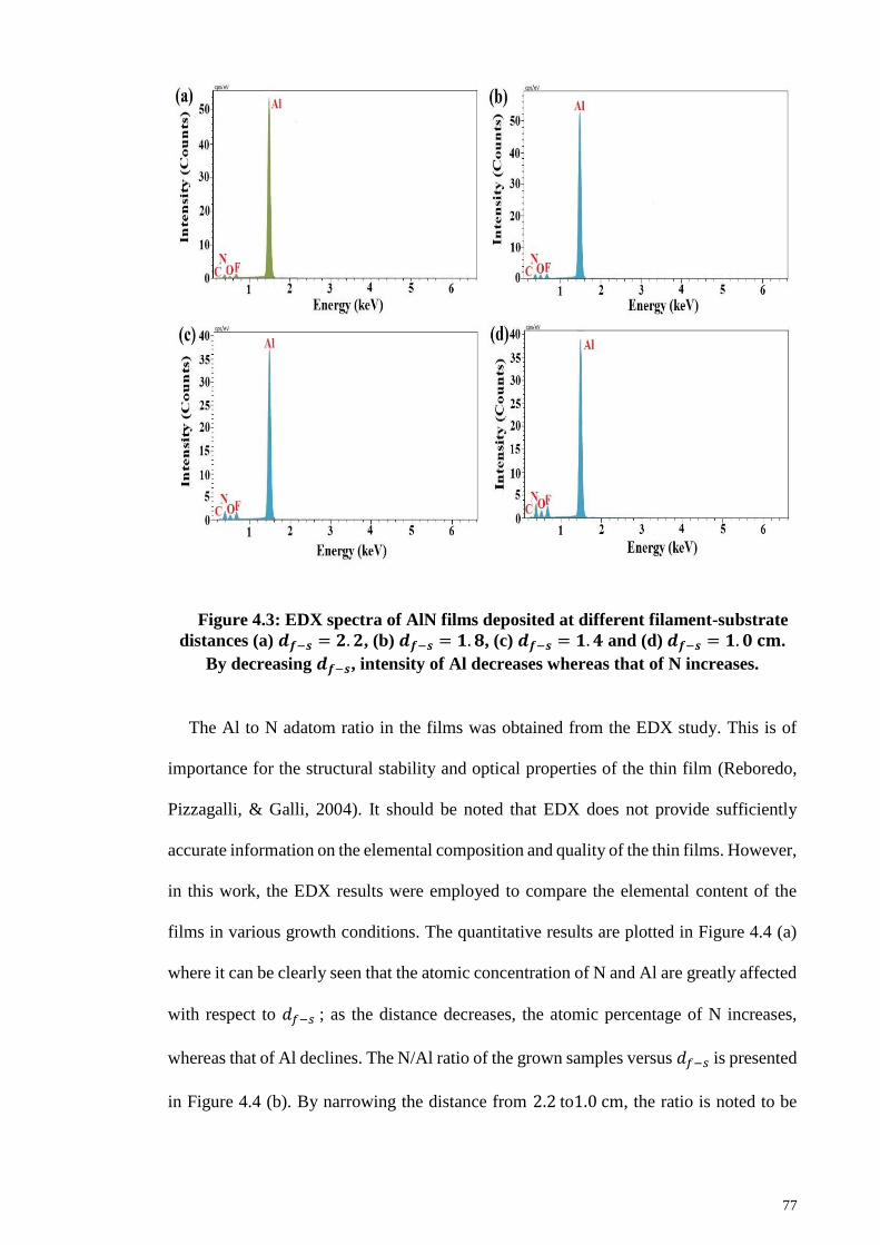
77
Figure 4.3: EDX spectra of AlN films deposited at different filament-substrate
distances (a) 𝒅𝒇−𝒔 = 𝟐. 𝟐, (b) 𝒅𝒇−𝒔 = 𝟏. 𝟖, (c) 𝒅𝒇−𝒔 = 𝟏. 𝟒 and (d) 𝒅𝒇−𝒔 = 𝟏. 𝟎 𝐜𝐦.
By decreasing 𝒅𝒇−𝒔, intensity of Al decreases whereas that of N increases.
The Al to N adatom ratio in the films was obtained from the EDX study. This is of
importance for the structural stability and optical properties of the thin film (Reboredo,
Pizzagalli, & Galli, 2004). It should be noted that EDX does not provide sufficiently
accurate information on the elemental composition and quality of the thin films. However,
in this work, the EDX results were employed to compare the elemental content of the
films in various growth conditions. The quantitative results are plotted in Figure 4.4 (a)
where it can be clearly seen that the atomic concentration of N and Al are greatly affected
with respect to 𝑑𝑓−𝑠 ; as the distance decreases, the atomic percentage of N increases,
whereas that of Al declines. The N/Al ratio of the grown samples versus 𝑑𝑓−𝑠 is presented
in Figure 4.4 (b). By narrowing the distance from 2.2 to1.0 cm, the ratio is noted to be
78
significantly increased and a balanced composition obtained for the AlN films deposited
at 𝑑𝑓−𝑠 = 1.0 cm.
The dependence of atomic percentage of Al and N on 𝑑𝑓−𝑠 can be related to the energy
of the growth species upon reaching the substrate. As a versatile tool, the hot filament
plays a key role in the growth process. It can simultaneously produce Al radicals and
excited N2 molecules through the evaporation of Al wires placed on the filament and the
excitation of N2 molecules in the vicinity of the filament, respectively (Chong, Goh, Dee,
& Rahman, 2012). The heated filament also contributes to heating the surface of the
growing film.
The applied RF power dissociates the excited N2 molecules producing N radicals and
ions depending on the magnitude of the applied RF power. These excited Al and N
radicals then will travel towards the substrate surface and upon reaching its growth sites
the surface reactions between these radicals and the substrates determine the sticking and
diffusing probability of these radicals into the film structure. Narrowing the gap between
the filament and substrate increases the radiant heat of the filament on the growth surface
and also reduces the probability of gas-phase reactions. Thus, the impact energy of the
radicals on the growth surface is increased. This increases the surface temperature and
can enhance the growth rate through the higher sticking probability (Chong, Goh, Dee, &
Rahman, 2013). However, the high bombardments of the growth surface with excited N
atoms or ions can also have the adverse effect of sputtering of atoms on the surface. The
higher mobility of the growth species on the surface of the substrate ensures that they
reach suitable growth sites for diffusion. As a result, less free metallic Al adatoms are left
on the surface of substrate as N atoms are bonded to the Al ones resulting in an increase
in the N/Al ratio in the AlN thin films and improving of the films quality and crystallinity.
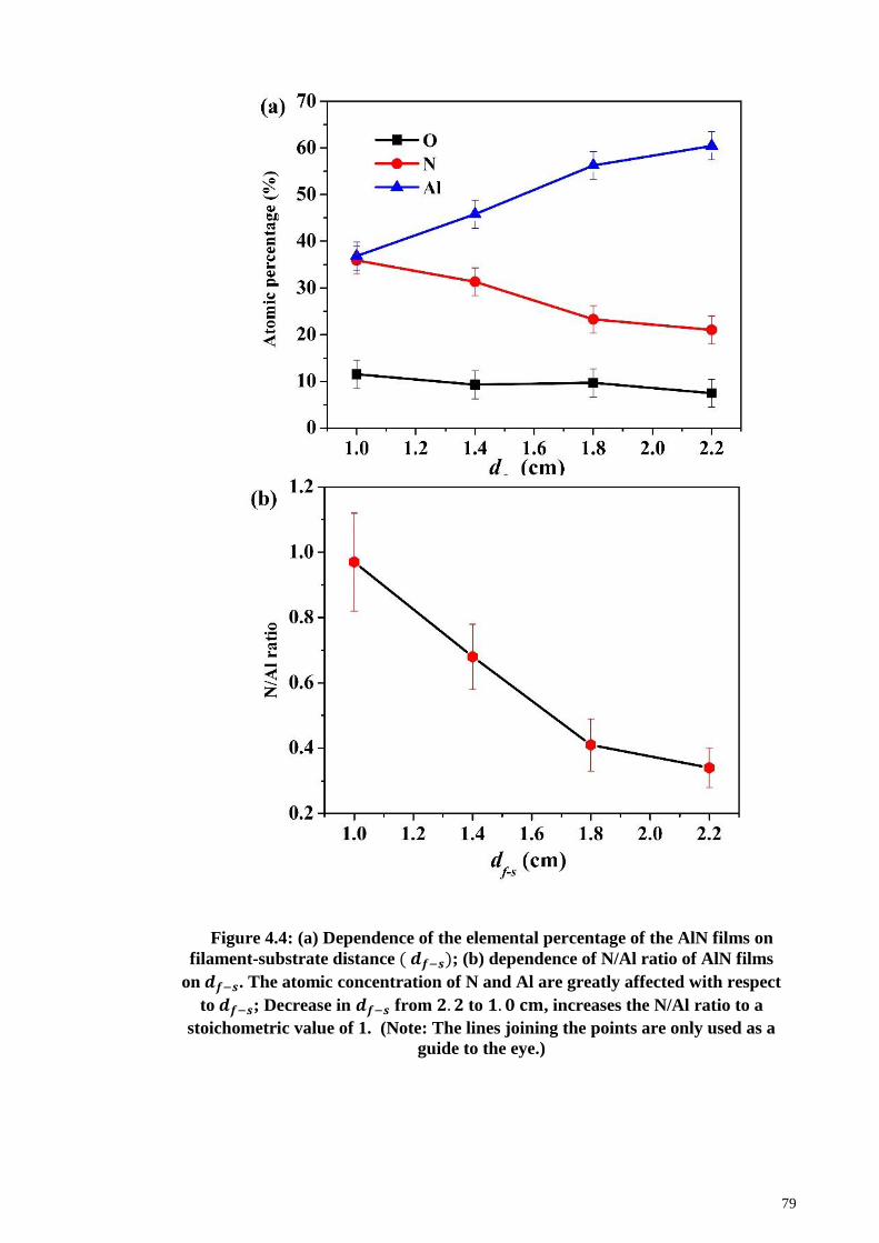
79
Figure 4.4: (a) Dependence of the elemental percentage of the AlN films on
filament-substrate distance ( 𝒅𝒇−𝒔); (b) dependence of N/Al ratio of AlN films
on 𝒅𝒇−𝒔. The atomic concentration of N and Al are greatly affected with respect
to 𝒅𝒇−𝒔; Decrease in 𝒅𝒇−𝒔 from 𝟐. 𝟐 to 𝟏. 𝟎 𝐜𝐦, increases the N/Al ratio to a
stoichometric value of 1. (Note: The lines joining the points are only used as a
guide to the eye.)
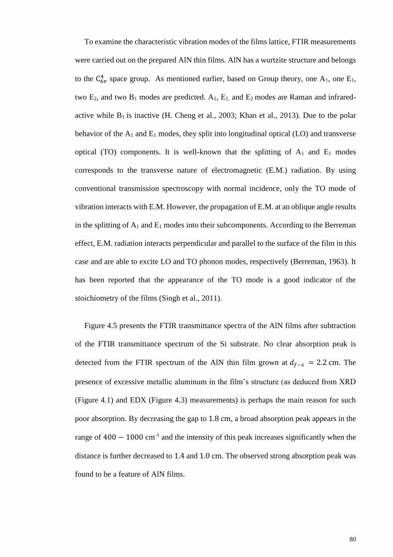
80
To examine the characteristic vibration modes of the films lattice, FTIR measurements
were carried out on the prepared AlN thin films. AlN has a wurtzite structure and belongs
to the C6𝑣4 space group. As mentioned earlier, based on Group theory, one A1, one E1,
two E2, and two B1 modes are predicted. A1, E1, and E2 modes are Raman and infrared-
active while B1 is inactive (H. Cheng et al., 2003; Khan et al., 2013). Due to the polar
behavior of the A1 and E1 modes, they split into longitudinal optical (LO) and transverse
optical (TO) components. It is well-known that the splitting of A1 and E1 modes
corresponds to the transverse nature of electromagnetic (E.M.) radiation. By using
conventional transmission spectroscopy with normal incidence, only the TO mode of
vibration interacts with E.M. However, the propagation of E.M. at an oblique angle results
in the splitting of A1 and E1 modes into their subcomponents. According to the Berreman
effect, E.M. radiation interacts perpendicular and parallel to the surface of the film in this
case and are able to excite LO and TO phonon modes, respectively (Berreman, 1963). It
has been reported that the appearance of the TO mode is a good indicator of the
stoichiometry of the films (Singh et al., 2011).
Figure 4.5 presents the FTIR transmittance spectra of the AlN films after subtraction
of the FTIR transmittance spectrum of the Si substrate. No clear absorption peak is
detected from the FTIR spectrum of the AlN thin film grown at 𝑑𝑓−𝑠 = 2.2 cm. The
presence of excessive metallic aluminum in the film’s structure (as deduced from XRD
(Figure 4.1) and EDX (Figure 4.3) measurements) is perhaps the main reason for such
poor absorption. By decreasing the gap to 1.8 cm, a broad absorption peak appears in the
range of 400 − 1000 cm-1 and the intensity of this peak increases significantly when the
distance is further decreased to 1.4 and 1.0 cm. The observed strong absorption peak was
found to be a feature of AlN films.
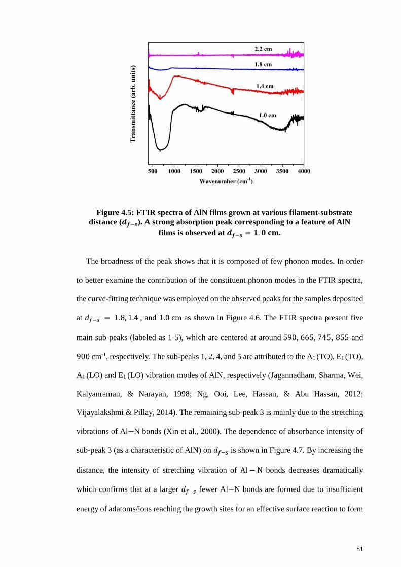
81
Figure 4.5: FTIR spectra of AlN films grown at various filament-substrate
distance (𝒅𝒇−𝒔). A strong absorption peak corresponding to a feature of AlN
films is observed at 𝒅𝒇−𝒔 = 𝟏. 𝟎 𝐜𝐦.
The broadness of the peak shows that it is composed of few phonon modes. In order
to better examine the contribution of the constituent phonon modes in the FTIR spectra,
the curve-fitting technique was employed on the observed peaks for the samples deposited
at 𝑑𝑓−𝑠 = 1.8, 1.4 , and 1.0 cm as shown in Figure 4.6. The FTIR spectra present five
main sub-peaks (labeled as 1-5), which are centered at around 590, 665, 745, 855 and
900 cm-1, respectively. The sub-peaks 1, 2, 4, and 5 are attributed to the A1 (TO), E1 (TO),
A1 (LO) and E1 (LO) vibration modes of AlN, respectively (Jagannadham, Sharma, Wei,
Kalyanraman, & Narayan, 1998; Ng, Ooi, Lee, Hassan, & Abu Hassan, 2012;
Vijayalakshmi & Pillay, 2014). The remaining sub-peak 3 is mainly due to the stretching
vibrations of Al−N bonds (Xin et al., 2000). The dependence of absorbance intensity of
sub-peak 3 (as a characteristic of AlN) on 𝑑𝑓−𝑠 is shown in Figure 4.7. By increasing the
distance, the intensity of stretching vibration of Al − N bonds decreases dramatically
which confirms that at a larger 𝑑𝑓−𝑠 fewer Al−N bonds are formed due to insufficient
energy of adatoms/ions reaching the growth sites for an effective surface reaction to form
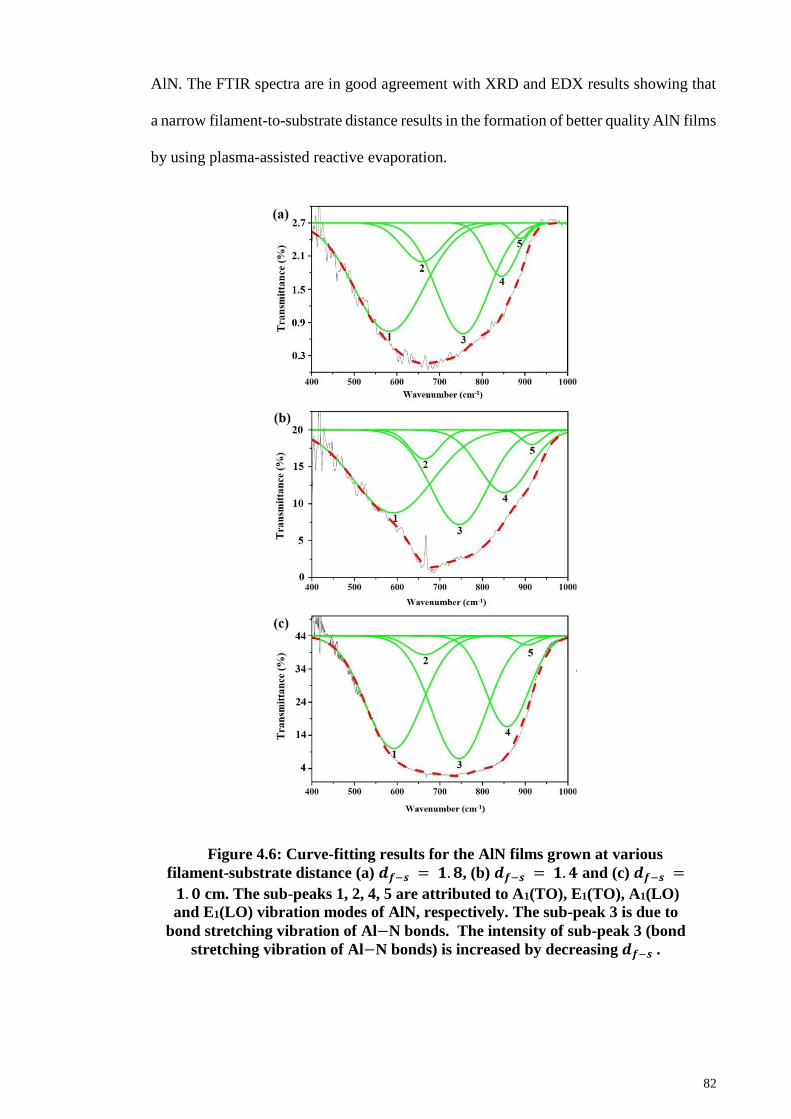
82
AlN. The FTIR spectra are in good agreement with XRD and EDX results showing that
a narrow filament-to-substrate distance results in the formation of better quality AlN films
by using plasma-assisted reactive evaporation.
Figure 4.6: Curve-fitting results for the AlN films grown at various
filament-substrate distance (a) 𝒅𝒇−𝒔 = 𝟏. 𝟖, (b) 𝒅𝒇−𝒔 = 𝟏. 𝟒 and (c) 𝒅𝒇−𝒔 =
𝟏. 𝟎 cm. The sub-peaks 1, 2, 4, 5 are attributed to A1(TO), E1(TO), A1(LO)
and E1(LO) vibration modes of AlN, respectively. The sub-peak 3 is due to
bond stretching vibration of Al−N bonds. The intensity of sub-peak 3 (bond
stretching vibration of Al−N bonds) is increased by decreasing 𝒅𝒇−𝒔 .
83
Figure 4.7: Dependence of intensity of bond stretching vibration of Al−N
bonds on filament-substrate distance (𝒅𝒇−𝒔). The intensity of bond stretching
vibration of Al−N bonds is increased by decreasing 𝒅𝒇−𝒔 .
4.3 Effects of RF Power on Crystallinity, Morphology, Composition and Optical
Properties of Indium Nitride Thin Films
Figure 4.8 shows the XRD patterns of InN samples prepared at different RF powers
(50–250 W). Five major peaks are observed from the XRD pattern of the InN films
deposited at RF power of 50 W. The peaks centred at 2θ = 30.50°, 35.40°, 50.90° and
60.70° are assigned to (222), (400), (440) and (622) planes of cubic indium oxide,
respectively (Jothibas et al., 2013). The peak at 2θ = 33° corresponds to (101) plane of
InN clearly indicating the existence of nitride- and oxide- phases in the InN film deposited
at the RF power of 50 W. The XRD pattern of the samples deposited at the RF powers of
100, 150, 200 and 250 W shows diffraction peaks at 2θ = 29.10°, 31.15°, 33°, 43°,
52°, 56.65°, 61.45° and 62.60° that corresponds to the (100), (002), (101), (102), (110),
(103), (112) and (201) planes of wurtzite InN, respectively. The peak positions are in
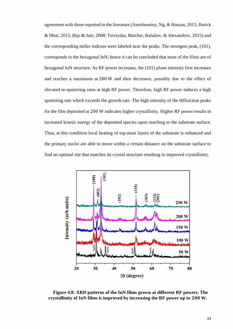
84
agreement with those reported in the literature (Amirhoseiny, Ng, & Hassan, 2015; Barick
& Dhar, 2015; Biju & Jain, 2008; Terziyska, Butcher, Rafailov, & Alexandrov, 2015) and
the corresponding miller indexes were labeled near the peaks. The strongest peak, (101),
corresponds to the hexagonal InN; hence it can be concluded that most of the films are of
hexagonal InN structure. As RF power increases, the (101) plane intensity first increases
and reaches a maximum at 200 W and then decreases, possibly due to the effect of
elevated re-sputtering rates at high RF power. Therefore, high RF power induces a high
sputtering rate which exceeds the growth rate. The high intensity of the diffraction peaks
for the film deposited at 200 W indicates higher crystallinity. Higher RF power results in
increased kinetic energy of the deposited species upon reaching to the substrate surface.
Thus, at this condition local heating of top-most layers of the substrate is enhanced and
the primary nuclei are able to move within a certain distance on the substrate surface to
find an optimal site that matches its crystal structure resulting in improved crystallinity.
Figure 4.8: XRD patterns of the InN films grown at different RF powers. The
crystallinity of InN films is improved by increasing the RF power up to 𝟐𝟎𝟎 W.
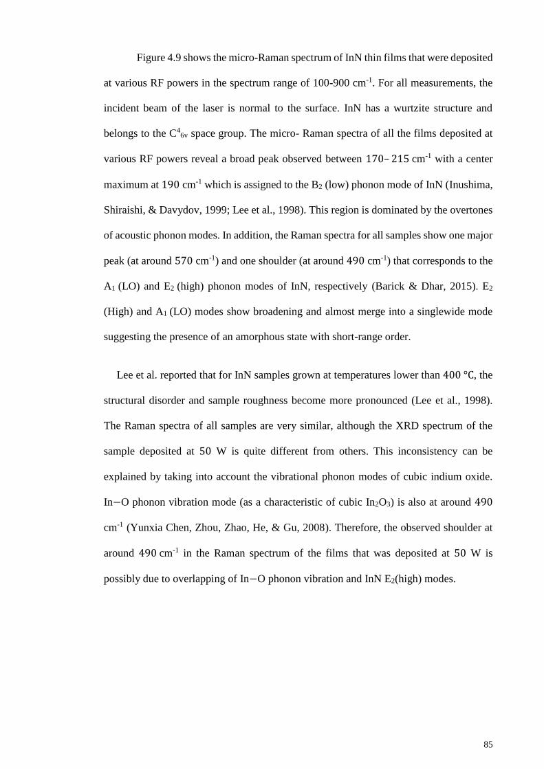
85
Figure 4.9 shows the micro-Raman spectrum of InN thin films that were deposited
at various RF powers in the spectrum range of 100-900 cm-1. For all measurements, the
incident beam of the laser is normal to the surface. InN has a wurtzite structure and
belongs to the C46v space group. The micro- Raman spectra of all the films deposited at
various RF powers reveal a broad peak observed between 170– 215 cm-1 with a center
maximum at 190 cm-1 which is assigned to the B2 (low) phonon mode of InN (Inushima,
Shiraishi, & Davydov, 1999; Lee et al., 1998). This region is dominated by the overtones
of acoustic phonon modes. In addition, the Raman spectra for all samples show one major
peak (at around 570 cm-1) and one shoulder (at around 490 cm-1) that corresponds to the
A1 (LO) and E2 (high) phonon modes of InN, respectively (Barick & Dhar, 2015). E2
(High) and A1 (LO) modes show broadening and almost merge into a singlewide mode
suggesting the presence of an amorphous state with short-range order.
Lee et al. reported that for InN samples grown at temperatures lower than 400 °C, the
structural disorder and sample roughness become more pronounced (Lee et al., 1998).
The Raman spectra of all samples are very similar, although the XRD spectrum of the
sample deposited at 50 W is quite different from others. This inconsistency can be
explained by taking into account the vibrational phonon modes of cubic indium oxide.
In−O phonon vibration mode (as a characteristic of cubic In2O3) is also at around 490
cm-1 (Yunxia Chen, Zhou, Zhao, He, & Gu, 2008). Therefore, the observed shoulder at
around 490 cm-1 in the Raman spectrum of the films that was deposited at 50 W is
possibly due to overlapping of In−O phonon vibration and InN E2(high) modes.
86
Figure 4.9: Raman spectra of the InN thin films that were deposited at
different applied RF powers. B2 (low), E2(high) and A1(LO) phonon modes of
InN are observed from the Raman spectra.
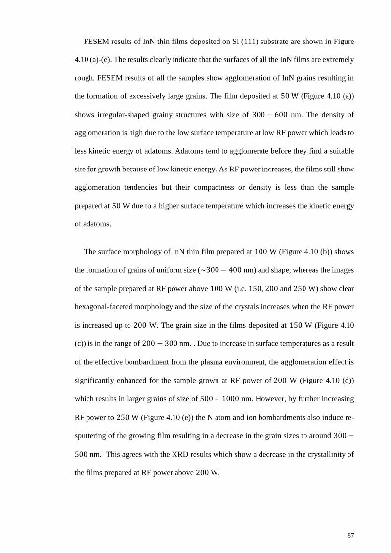
87
FESEM results of InN thin films deposited on Si (111) substrate are shown in Figure
4.10 (a)-(e). The results clearly indicate that the surfaces of all the InN films are extremely
rough. FESEM results of all the samples show agglomeration of InN grains resulting in
the formation of excessively large grains. The film deposited at 50 W (Figure 4.10 (a))
shows irregular-shaped grainy structures with size of 300 − 600 nm. The density of
agglomeration is high due to the low surface temperature at low RF power which leads to
less kinetic energy of adatoms. Adatoms tend to agglomerate before they find a suitable
site for growth because of low kinetic energy. As RF power increases, the films still show
agglomeration tendencies but their compactness or density is less than the sample
prepared at 50 W due to a higher surface temperature which increases the kinetic energy
of adatoms.
The surface morphology of InN thin film prepared at 100 W (Figure 4.10 (b)) shows
the formation of grains of uniform size (~300 − 400 nm) and shape, whereas the images
of the sample prepared at RF power above 100 W (i.e. 150, 200 and 250 W) show clear
hexagonal-faceted morphology and the size of the crystals increases when the RF power
is increased up to 200 W. The grain size in the films deposited at 150 W (Figure 4.10
(c)) is in the range of 200 − 300 nm. . Due to increase in surface temperatures as a result
of the effective bombardment from the plasma environment, the agglomeration effect is
significantly enhanced for the sample grown at RF power of 200 W (Figure 4.10 (d))
which results in larger grains of size of 500 – 1000 nm. However, by further increasing
RF power to 250 W (Figure 4.10 (e)) the N atom and ion bombardments also induce re-
sputtering of the growing film resulting in a decrease in the grain sizes to around 300 −
500 nm. This agrees with the XRD results which show a decrease in the crystallinity of
the films prepared at RF power above 200 W.
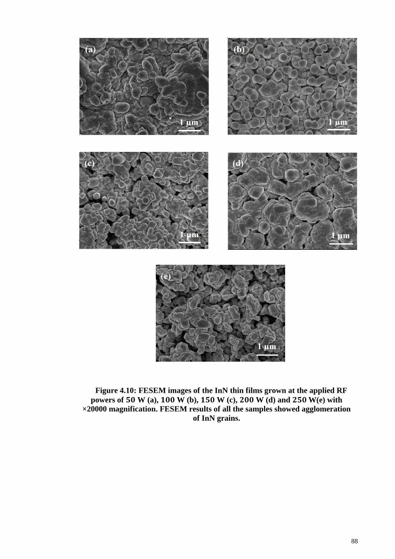
88
Figure 4.10: FESEM images of the InN thin films grown at the applied RF
powers of 𝟓𝟎 W (a), 𝟏𝟎𝟎 W (b), 𝟏𝟓𝟎 W (c), 𝟐𝟎𝟎 W (d) and 𝟐𝟓𝟎 W(e) with
×20000 magnification. FESEM results of all the samples showed agglomeration
of InN grains.
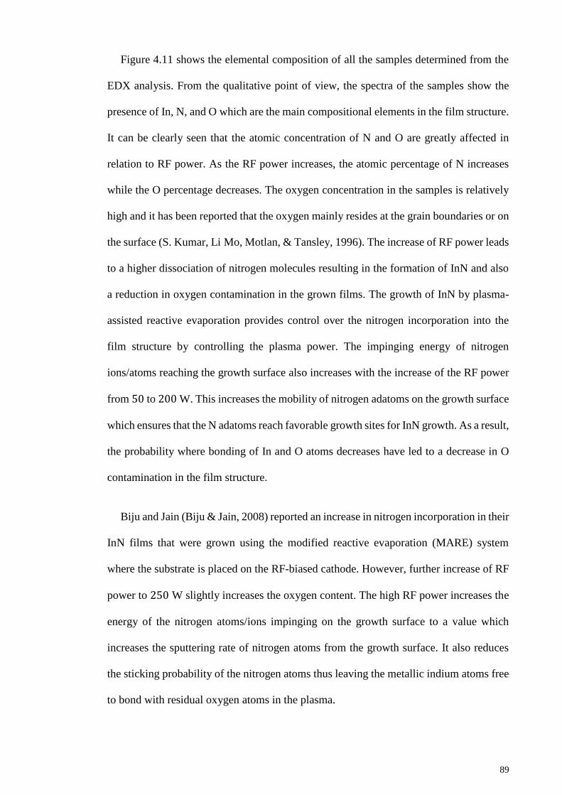
89
Figure 4.11 shows the elemental composition of all the samples determined from the
EDX analysis. From the qualitative point of view, the spectra of the samples show the
presence of In, N, and O which are the main compositional elements in the film structure.
It can be clearly seen that the atomic concentration of N and O are greatly affected in
relation to RF power. As the RF power increases, the atomic percentage of N increases
while the O percentage decreases. The oxygen concentration in the samples is relatively
high and it has been reported that the oxygen mainly resides at the grain boundaries or on
the surface (S. Kumar, Li Mo, Motlan, & Tansley, 1996). The increase of RF power leads
to a higher dissociation of nitrogen molecules resulting in the formation of InN and also
a reduction in oxygen contamination in the grown films. The growth of InN by plasma-
assisted reactive evaporation provides control over the nitrogen incorporation into the
film structure by controlling the plasma power. The impinging energy of nitrogen
ions/atoms reaching the growth surface also increases with the increase of the RF power
from 50 to 200 W. This increases the mobility of nitrogen adatoms on the growth surface
which ensures that the N adatoms reach favorable growth sites for InN growth. As a result,
the probability where bonding of In and O atoms decreases have led to a decrease in O
contamination in the film structure.
Biju and Jain (Biju & Jain, 2008) reported an increase in nitrogen incorporation in their
InN films that were grown using the modified reactive evaporation (MARE) system
where the substrate is placed on the RF-biased cathode. However, further increase of RF
power to 250 W slightly increases the oxygen content. The high RF power increases the
energy of the nitrogen atoms/ions impinging on the growth surface to a value which
increases the sputtering rate of nitrogen atoms from the growth surface. It also reduces
the sticking probability of the nitrogen atoms thus leaving the metallic indium atoms free
to bond with residual oxygen atoms in the plasma.
90
Figure 4.11: (a) Dependence of the elemental percentage of the InN films on
RF power; (b) dependence of N/In ratio of AlN films on RF power. The atomic
concentration of N and Al are greatly affected with respect to RF power.
Increase in RF power from 𝟓𝟎 to 𝟐𝟓𝟎 W, increases the N/In ratio to a
stoichometric value of 1. (Note: The lines joining the points are only used as a
guide to the eye.)
91
In order to obtain the optical band gap of the InN films, the deposition was performed
on quartz substrates. Figure 4.12 displays the plots of (𝛼ℎ𝜐)2 versus photon energy (ℎ𝜐)
where 𝛼 is the absorption coefficient at the specified photon energy. Due to rough surface
of the grown films, a very weak reflectance was observed for the films. Hence 𝛼 was
calculated by using the transmission and thickness of the films (𝛼 = −(1/d)ln[T]) (Q.
Guo et al., 2008). The value of the optical band gap is determined by extrapolating the
linear part of the curve to the energy axis in Figure 4.12.
The thickness and obtained band gap energy of each sample are summarized in Table
4.1. The optical band gap energy (𝐸𝑔) of the films deposited at 100, 150, 200 and 250 W
are 2.28, 2.28, 2.18 and 2.13 eV, respectively. These values are close to the 𝐸𝑔 of
polycrystalline InN as previously reported (K. S. A. Butcher & Tansley, 2005) . The
obtained values are larger than the recently reported band gap energy value of pure InN
(e. g., 0.7 eV). As reported by other researchers, possible reasons for the high band gap
value are the Moss-Burstein (MB) shift, the presence of oxygen impurity, and other
stoichiometry-related defects (T. Matsuoka et al., 2004; T. V. Shubina et al., 2004;
Sundaresan, Vasumathi, Ravichandran, Ravikumar, & Sakthivel, 2012). The sample
deposited at 50 W shows largest band gap value which equals to 2.35 eV. This is probably
due to the very high oxygen content and formation of oxynitride alloys within the films
(Alexandrov, Butcher, & Wintrebert-Fouquet, 2004). Segregated oxygen species could
substitute N atoms as InO and form InOyN1-y alloys resulting in the higher band gap values
of the films especially for those deposited at the lowest RF power of 50 W, which has the
highest oxygen impurities in the film structure.
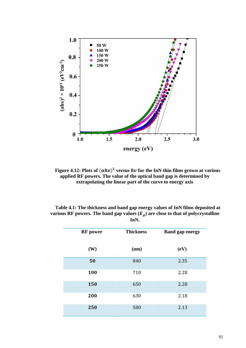
92
Figure 4.12: Plots of (𝜶𝒉𝝊)𝟐 versus 𝒉𝝊 for the InN thin films grown at various
applied RF powers. The value of the optical band gap is determined by
extrapolating the linear part of the curve to energy axis
Table 4.1: The thickness and band gap energy values of InN films deposited at
various RF powers. The band gap values (𝑬𝒈) are close to that of polycrystalline
InN.
RF power
(W)
Thickness
(nm)
Band gap energy
(eV)
𝟓𝟎 840 2.35
𝟏𝟎𝟎 710 2.28
𝟏𝟓𝟎 650 2.28
𝟐𝟎𝟎 630 2.18
𝟐𝟓𝟎 580 2.13
93
4.4 Summary
In this chapter the results associated with the growth of AlN and InN thin films by
plasma-assisted reactive evaporation were presented and discussed. It was shown that
filament-to-substrate distance and plasma RF power are the most dominant parameters
which have great impacts on the properties of AlN and InN thin films, respectively. The
XRD results of AlN thin films showed that by decreasing the distance, the intensity of the
peak corresponding to metallic Al decreases while that of AlN increases. EDX results
indicated that at lower filament-to-substrate distance, the incorporation of N into the AlN
films is enhanced and this was further confirmed by FTIR results. Also, the surface
morphology of the AlN thin films grown at the low distance is more uniform. Increasing
RF power resulted in the improved crystalinity of the InN films and also reduced the
oxygen impurities in the films. Large division from the reported value was observed for
the band gap energy of the InN films that where grown by plasma-assisted reactive
evaporation which was attributed to the Moss-Burstein (MB) shift and the presence of
oxygen impurities in the films.
94
CHAPTER 5:
ALUMINUM INDIUM NITRIDE THIN FILMS: STRUCTURE,
MORPHOLOGY AND OPTICAL PROPERTIES
5.1 Introduction
This chapter discusses the results of the studies on aluminum indium nitride (AlxIn1-
xN) thin films that were deposited by plasma-assisted dual source reactive evaporation.
The voltage applied to the filament holding the indium wire (VIn) and the nitrogen flow
rates appeared to be the most critical parameters in influencing the properties of the
produced thin films. In the first part of this chapter, the effects of VIn on the properties
of AlxIn1-xN thin films are discussed in regard to their structural, compositional,
morphological, and optical characteristics. The objective is to establish the role of VIn in
tuning the Al composition in the films. The second part of this chapter discusses the
effects of nitrogen flow rates on the properties of the two sets of films categorized as In-
rich and Al-rich AlxIn1-xN thin films selected for the study. The final part of this chapter
is devoted to the study of the effects of annealing on the properties of the selected AlxIn1-
xN thin films. The objective of this study is to investigate the stability of the properties of
the films and the incorporation of oxygen impurity in their structures at elevated
temperatures. The results are useful in determining the temperature range which is
suitable for application of the AlxIn1-xN thin films deposited by this technique in various
opto-electronic devices.
5.2 The Role of Filament Temperature on the Growth of Aluminum Indium
Nitride Thin Films
The elemental composition of the AlxIn1-xN films deposited at different applied
voltages (VIn) was analyzed using x-ray photoelectron spectra (XPS). The In3d5/2 core-
level photoelectron spectra of the AlxIn1-xN films prepared at VIn = 65 to 80 V are shown
95
in Figure 5.1. A significant increase in the intensity of the In3d5/2 core-level is observed
when VIn is increased, implying that higher amounts of In adatoms were incorporated into
the AlxIn1-xN film structure at higher voltages. The core-level photoelectron spectra for
all samples were deconvoluted into three main sub-peaks centered at 445.3 eV, 444.3 eV
and 443.3 eV which are attributed to In−O, In−N and In-In bonds, respectively (A. K. S.
Chauhan, Kumar, & Gupta, 2015; Lebedev et al., 2006). The corresponding Al2p core-
level photoelectron spectra of AlxIn1-xN films deposited at VIn = 65 to 80 V are presented
in the inset of Figure 5.1 (a)-(d). All the spectra were also deconvoluted into three main
components at 75 ± 0.2 eV , 74 ± 0.1 eV and 72.6 ± 0.2 eV which are assigned to
Al−O, Al−N and Al−Al bonds, respectively (Rosenberger, Baird, McCullen, Auner, &
Shreve, 2008; You, Ito, Tu, & Goto, 2013). The appearance of In−In, In−O, Al−Al and
Al−O bonds could be due to the higher concentrations of reactive In and Al atoms
reaching the growth sites as-compared to the reactive N atoms and the high affinity of the
metallic adatoms to oxygen. An analysis on the chemical composition of the films
revealed that the estimated Al mole fractions (Al composition) in the AlxIn1-xN films, x,
are 0.64, 0.60, 0.18 and 0.10 as determined from the ratio of the area of the Al−N and
In−N peaks (Al−N/( Al−N+ In−N) (Suzuki et al., 2013)) for the films deposited at VIn
of 65, 70, 75 and 80 V, respectively.
Figure 5.2 displays the dependence of FIn temperature and aluminum incorporation
into the composition of the films on the applied voltage to FIn (VIn). A rise from 1010 ±
10 °C to 1105 ± 10 °C was recorded in the FIn temperature by increasing VIn from 65
to 80 V, which clearly shows that VIn controlled the FIn temperature. The increase in the
FIn temperature have resulted in enhanced generation and deposition of reactive indium
atoms at the substrate surface and, hence, decreased the aluminum mole fraction (x) in
the films’ composition. Guo et al. (Q. X. Guo et al., 2007) reported similar tuning
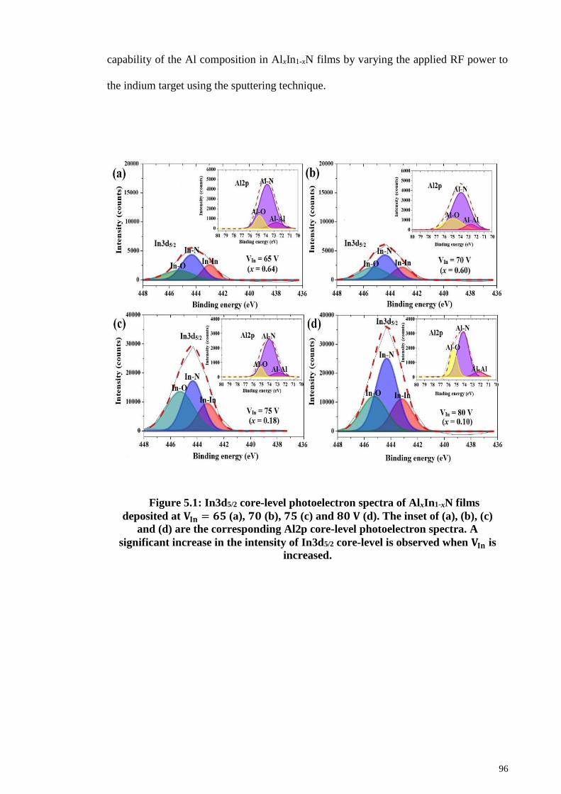
96
capability of the Al composition in AlxIn1-xN films by varying the applied RF power to
the indium target using the sputtering technique.
Figure 5.1: In3d5/2 core-level photoelectron spectra of AlxIn1-xN films
deposited at 𝐕𝐈𝐧 = 𝟔𝟓 (a), 𝟕𝟎 (b), 𝟕𝟓 (c) and 𝟖𝟎 𝐕 (d). The inset of (a), (b), (c)
and (d) are the corresponding Al2p core-level photoelectron spectra. A
significant increase in the intensity of In3d5/2 core-level is observed when 𝐕𝐈𝐧 is
increased.
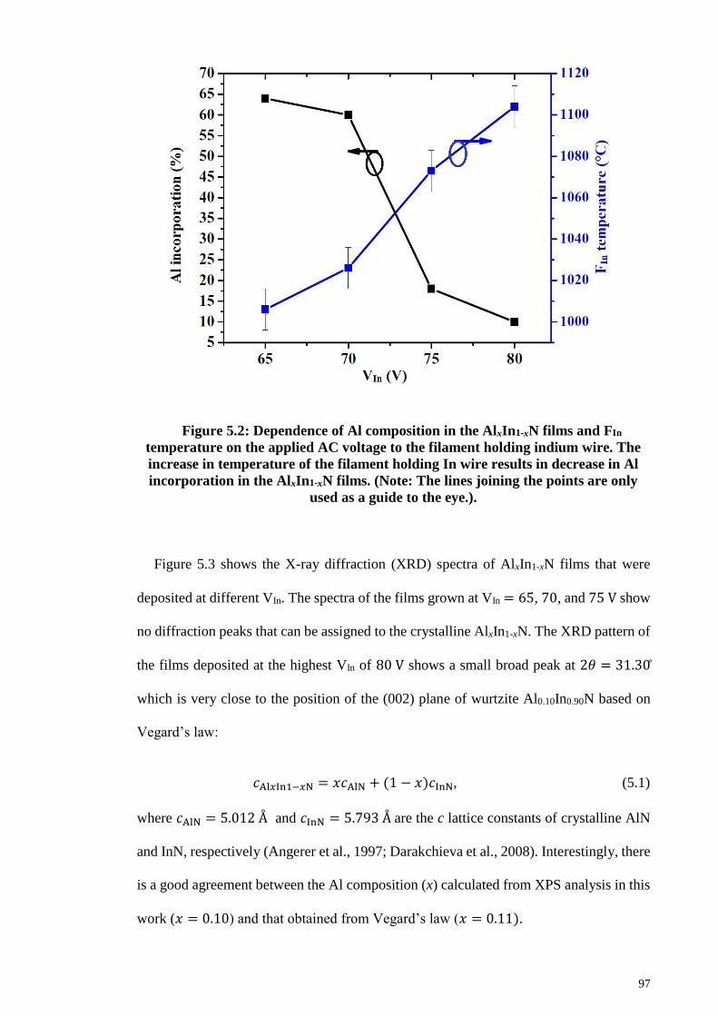
97
Figure 5.2: Dependence of Al composition in the AlxIn1-xN films and FIn
temperature on the applied AC voltage to the filament holding indium wire. The
increase in temperature of the filament holding In wire results in decrease in Al
incorporation in the AlxIn1-xN films. (Note: The lines joining the points are only
used as a guide to the eye.).
Figure 5.3 shows the X-ray diffraction (XRD) spectra of AlxIn1-xN films that were
deposited at different VIn. The spectra of the films grown at VIn = 65, 70, and 75 V show
no diffraction peaks that can be assigned to the crystalline AlxIn1-xN. The XRD pattern of
the films deposited at the highest VIn of 80 V shows a small broad peak at 2𝜃 = 31.30̊
which is very close to the position of the (002) plane of wurtzite Al0.10In0.90N based on
Vegard’s law:
𝑐Al𝑥In1−𝑥N = 𝑥𝑐AlN + (1 − 𝑥)𝑐InN, (5.1)
where 𝑐AlN = 5.012 Å and 𝑐InN = 5.793 Å are the c lattice constants of crystalline AlN
and InN, respectively (Angerer et al., 1997; Darakchieva et al., 2008). Interestingly, there
is a good agreement between the Al composition (x) calculated from XPS analysis in this
work (𝑥 = 0.10) and that obtained from Vegard’s law (𝑥 = 0.11).
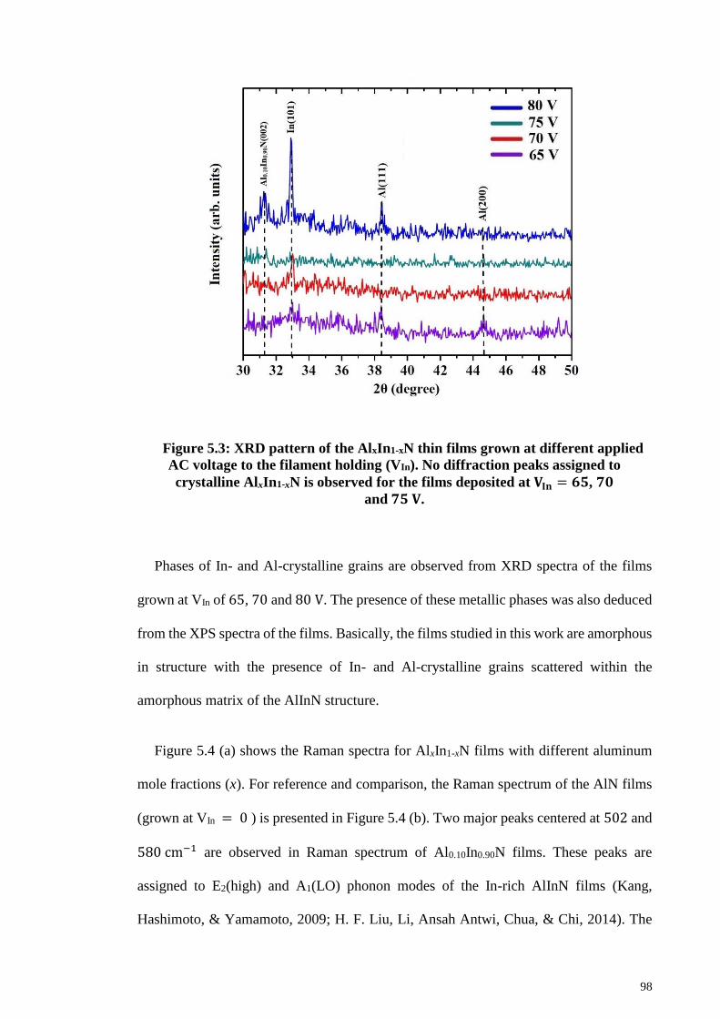
98
Figure 5.3: XRD pattern of the AlxIn1-xN thin films grown at different applied
AC voltage to the filament holding (VIn). No diffraction peaks assigned to
crystalline AlxIn1-xN is observed for the films deposited at 𝐕𝐈𝐧 = 𝟔𝟓, 𝟕𝟎
and 𝟕𝟓 𝐕.
Phases of In- and Al-crystalline grains are observed from XRD spectra of the films
grown at VIn of 65, 70 and 80 V. The presence of these metallic phases was also deduced
from the XPS spectra of the films. Basically, the films studied in this work are amorphous
in structure with the presence of In- and Al-crystalline grains scattered within the
amorphous matrix of the AlInN structure.
Figure 5.4 (a) shows the Raman spectra for AlxIn1-xN films with different aluminum
mole fractions (x). For reference and comparison, the Raman spectrum of the AlN films
(grown at VIn = 0 ) is presented in Figure 5.4 (b). Two major peaks centered at 502 and
580 cm−1 are observed in Raman spectrum of Al0.10In0.90N films. These peaks are
assigned to E2(high) and A1(LO) phonon modes of the In-rich AlInN films (Kang,
Hashimoto, & Yamamoto, 2009; H. F. Liu, Li, Ansah Antwi, Chua, & Chi, 2014). The
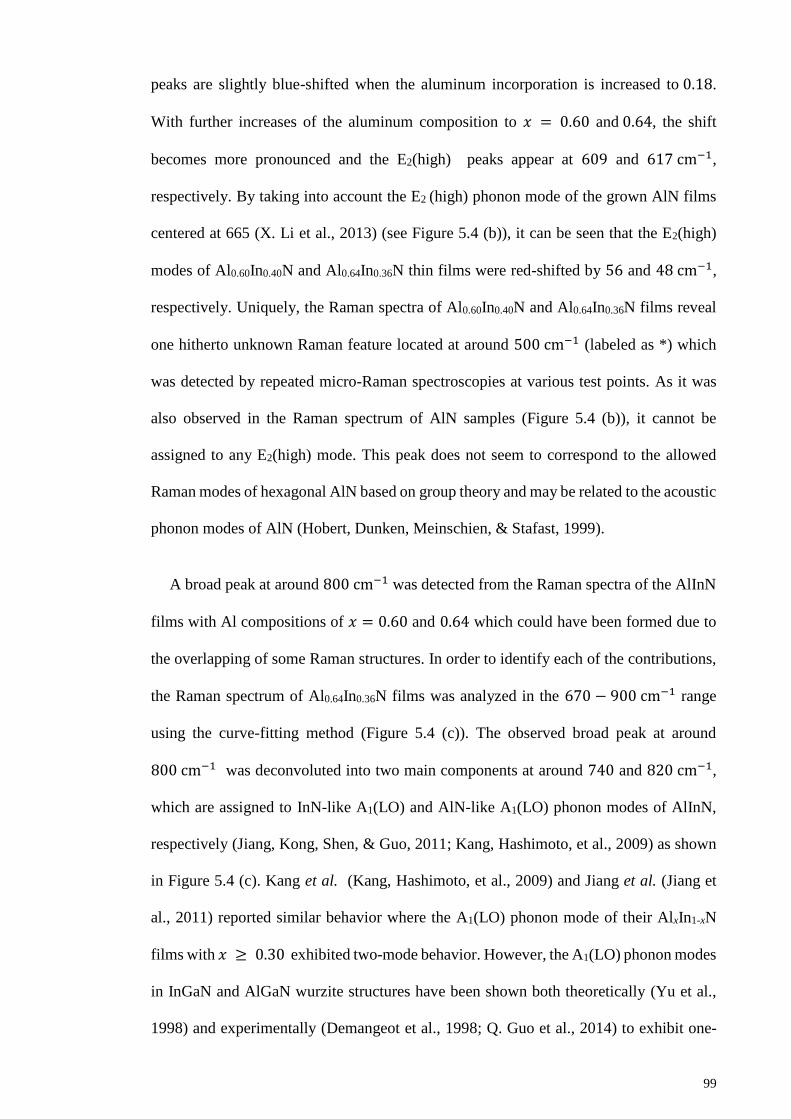
99
peaks are slightly blue-shifted when the aluminum incorporation is increased to 0.18.
With further increases of the aluminum composition to 𝑥 = 0.60 and 0.64, the shift
becomes more pronounced and the E2(high) peaks appear at 609 and 617 cm−1,
respectively. By taking into account the E2 (high) phonon mode of the grown AlN films
centered at 665 (X. Li et al., 2013) (see Figure 5.4 (b)), it can be seen that the E2(high)
modes of Al0.60In0.40N and Al0.64In0.36N thin films were red-shifted by 56 and 48 cm−1,
respectively. Uniquely, the Raman spectra of Al0.60In0.40N and Al0.64In0.36N films reveal
one hitherto unknown Raman feature located at around 500 cm−1 (labeled as *) which
was detected by repeated micro-Raman spectroscopies at various test points. As it was
also observed in the Raman spectrum of AlN samples (Figure 5.4 (b)), it cannot be
assigned to any E2(high) mode. This peak does not seem to correspond to the allowed
Raman modes of hexagonal AlN based on group theory and may be related to the acoustic
phonon modes of AlN (Hobert, Dunken, Meinschien, & Stafast, 1999).
A broad peak at around 800 cm−1 was detected from the Raman spectra of the AlInN
films with Al compositions of 𝑥 = 0.60 and 0.64 which could have been formed due to
the overlapping of some Raman structures. In order to identify each of the contributions,
the Raman spectrum of Al0.64In0.36N films was analyzed in the 670 − 900 cm−1 range
using the curve-fitting method (Figure 5.4 (c)). The observed broad peak at around
800 cm−1 was deconvoluted into two main components at around 740 and 820 cm−1,
which are assigned to InN-like A1(LO) and AlN-like A1(LO) phonon modes of AlInN,
respectively (Jiang, Kong, Shen, & Guo, 2011; Kang, Hashimoto, et al., 2009) as shown
in Figure 5.4 (c). Kang et al. (Kang, Hashimoto, et al., 2009) and Jiang et al. (Jiang et
al., 2011) reported similar behavior where the A1(LO) phonon mode of their AlxIn1-xN
films with 𝑥 ≥ 0.30 exhibited two-mode behavior. However, the A1(LO) phonon modes
in InGaN and AlGaN wurzite structures have been shown both theoretically (Yu et al.,
1998) and experimentally (Demangeot et al., 1998; Q. Guo et al., 2014) to exhibit one-
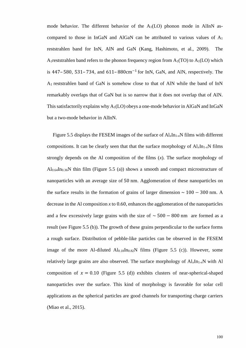
100
mode behavior. The different behavior of the A1(LO) phonon mode in AlInN as-
compared to those in InGaN and AlGaN can be attributed to various values of A1
reststrahlen band for InN, AlN and GaN (Kang, Hashimoto, et al., 2009). The
A1reststrahlen band refers to the phonon frequency region from A1(TO) to A1(LO) which
is 447– 580, 531– 734, and 611– 880cm−1 for InN, GaN, and AlN, respectively. The
A1 reststrahlen band of GaN is somehow close to that of AlN while the band of InN
remarkably overlaps that of GaN but is so narrow that it does not overlap that of AlN.
This satisfactorily explains why A1(LO) obeys a one-mode behavior in AlGaN and InGaN
but a two-mode behavior in AlInN.
Figure 5.5 displays the FESEM images of the surface of AlxIn1-xN films with different
compositions. It can be clearly seen that that the surface morphology of AlxIn1-xN films
strongly depends on the Al composition of the films (x). The surface morphology of
Al0.64In0.36N thin film (Figure 5.5 (a)) shows a smooth and compact microstructure of
nanoparticles with an average size of 50 nm. Agglomeration of these nanoparticles on
the surface results in the formation of grains of larger dimension ~ 100 − 300 nm. A
decrease in the Al composition x to 0.60, enhances the agglomeration of the nanoparticles
and a few excessively large grains with the size of ~ 500 − 800 nm are formed as a
result (see Figure 5.5 (b)). The growth of these grains perpendicular to the surface forms
a rough surface. Distribution of pebble-like particles can be observed in the FESEM
image of the more Al-diluted Al0.18In0.82N films (Figure 5.5 (c)). However, some
relatively large grains are also observed. The surface morphology of AlxIn1-xN with Al
composition of 𝑥 = 0.10 (Figure 5.5 (d)) exhibits clusters of near-spherical-shaped
nanoparticles over the surface. This kind of morphology is favorable for solar cell
applications as the spherical particles are good channels for transporting charge carriers
(Miao et al., 2015).
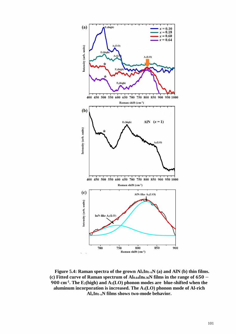
101
Figure 5.4: Raman spectra of the grown AlxIn1-xN (a) and AlN (b) thin films.
(c) Fitted curve of Raman spectrum of Al0.64In0.36N films in the range of 𝟔𝟓𝟎 −𝟗𝟎𝟎 cm-1. The E2(high) and A1(LO) phonon modes are blue-shifted when the
aluminum incorporation is increased. The A1(LO) phonon mode of Al-rich
AlxIn1-xN films shows two-mode behavior.
102
Figure 5.5: FESEM images of the AlxIn1-xN films with Al compositions of 𝒙 =𝟎. 𝟔𝟒 (a), 𝟎. 𝟔𝟎 (b), 𝟎. 𝟏𝟖 (c) and 𝟎. 𝟏𝟎 (d) with ×30000 magnification.
Agglomeration of grains are observed from the FESEM image of Al-rich AlxIn1-
xN films.
The optical properties of AlxIn1-xN films with different compositions were studied by
obtaining the transmittance and reflectance spectra of the films. Figure 5.6 (a) displays
the transmittance curves of the AlxIn1-xN films with Al compositions of 𝑥 =
0.10, 0.18, 0.60, and 0.64. In-rich films (𝑥 = 0.10 and 0.18) show an absorption in the
near-infrared (NIR) region and an insignificant transmittance (e. g., 𝑇~ 0%) in the range
of 300 − 1000 nm. As 𝑥 is increased towards the Al-rich region, the absorption edge of
the films shifts towards a shorter wavelength and the AlxIn1-xN films with a higher Al
content become more transparent in the visible and near-infrared (NIR) regions. In order
to further clarify the optical results, transmittance of the AlN film was also measured (see
inset in Figure 5.6 (a)). The sample was prepared in absence of FIn. The absorption edge
of the sample occurred at around 200 nm which is in good agreement with the reported
103
absorption edge wavelength of AlN films (Q. X. Guo, Tanaka, Nishio, & Ogawa, 2006;
H. T. Wang et al., 2014). Figure 5.6 (b) depicts the wavelength dependence of the optical
reflectance spectra of the AlInN films with different aluminum compositions (x). It can
be clearly observed that the minimum reflectance is shifted towards the longer
wavelength as x is reduced from 0.64 to 0.10. Since the minimum value of the reflection
occurs in the vicinity of the wavelength related to the optical band gap energy, the results
in Figure 5.6 (b) show that the band gap value of the AlInN films increases by increasing
x. An insignificant reflectance (e. g., 𝑅~ 3% ) at around 200 nm is obtained from the
optical reflectance spectrum of AlN films (see the inset of Figure 5.6 (b)) which is in good
agreement with the corresponding transmittance results shown in the inset of Figure 5.6
(a).
Figure 5.7 shows (𝛼ℎ𝜐)2 vs ℎ𝜐 curves for all of the deposited films. The direct band
gap of an AlxIn1-xN film was determined by extrapolating the linear part of the curves
down to the energy axis. It can be seen that the optical band gap of the AlxIn1-xN film
changes with the variation of the Al composition within the film’s structure. The optical
band gap of grown Al0.64In0.36N thin film is estimated to be 2.50 eV. As x decreases
to 0.60, 0.18, and 0.10 the band gap energies of the films are obtained at 2.33, 1.42,
and 1.08 eV, respectively. Such controlled tuning of the band gap energy is extremely
crucial for the application of AlInN alloys in multi-junction solar technology.
The 𝐸𝑔 value of pure AlN as-shown in the inset of Figure 5.7 is estimated to be 5.5 𝑒𝑉,
which is smaller than the value of 6.2 eV reported in previous works (Vurgaftman &
Meyer, 2003). It has been shown that the band gap of an AlN film decreases due to various
factors such as high carrier concentration, nonstoichiometric composition, and impose of
residual stresses as well as presence of structural defects and oxygen impurity in the film
structure (Persson et al., 2002; Yoshikawa et al., 1999). The AlN band gap energy
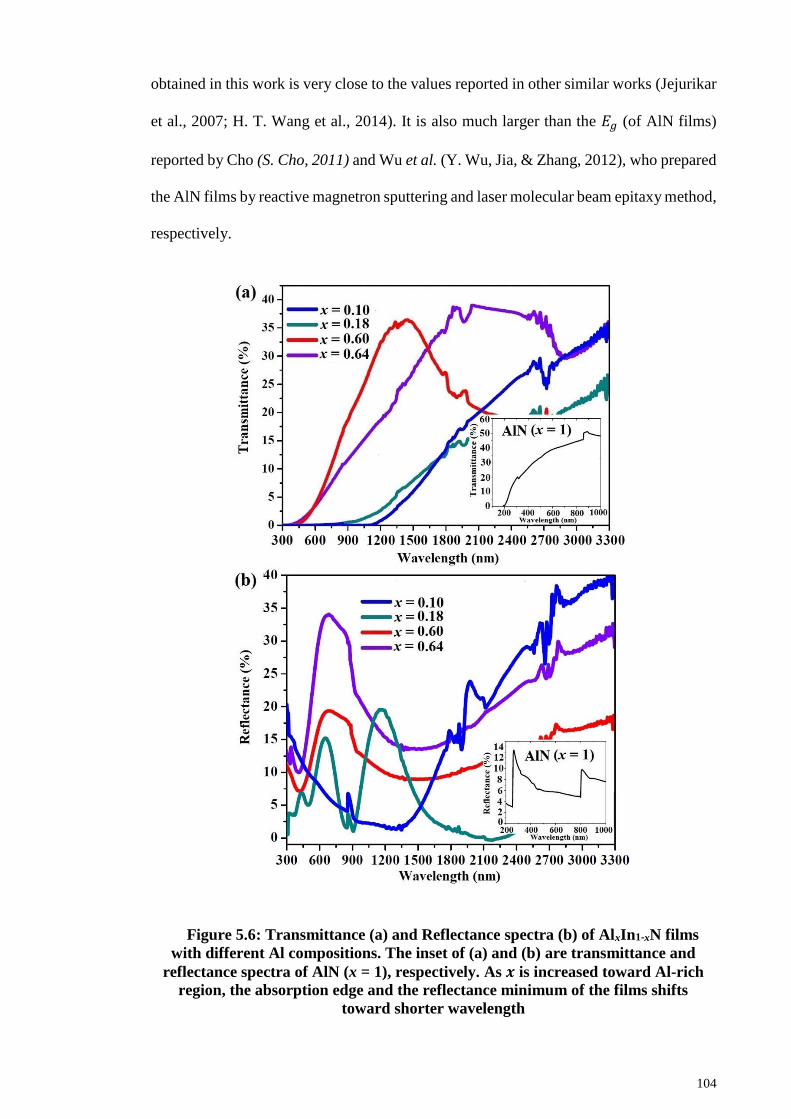
104
obtained in this work is very close to the values reported in other similar works (Jejurikar
et al., 2007; H. T. Wang et al., 2014). It is also much larger than the 𝐸𝑔 (of AlN films)
reported by Cho (S. Cho, 2011) and Wu et al. (Y. Wu, Jia, & Zhang, 2012), who prepared
the AlN films by reactive magnetron sputtering and laser molecular beam epitaxy method,
respectively.
Figure 5.6: Transmittance (a) and Reflectance spectra (b) of AlxIn1-xN films
with different Al compositions. The inset of (a) and (b) are transmittance and
reflectance spectra of AlN (x = 1), respectively. As 𝒙 is increased toward Al-rich
region, the absorption edge and the reflectance minimum of the films shifts
toward shorter wavelength
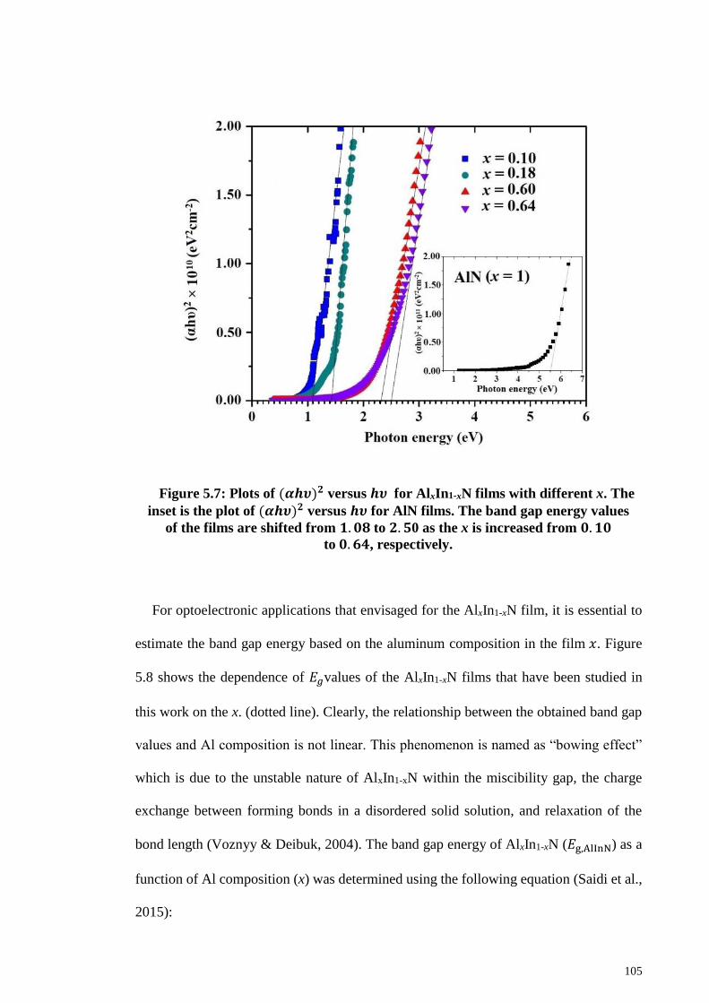
105
Figure 5.7: Plots of (𝜶𝒉𝝊)𝟐 versus 𝒉𝝊 for AlxIn1-xN films with different x. The
inset is the plot of (𝜶𝒉𝝊)𝟐 versus 𝒉𝝊 for AlN films. The band gap energy values
of the films are shifted from 𝟏. 𝟎𝟖 to 𝟐. 𝟓0 as the x is increased from 𝟎. 𝟏𝟎
to 𝟎. 𝟔𝟒, respectively.
For optoelectronic applications that envisaged for the AlxIn1-xN film, it is essential to
estimate the band gap energy based on the aluminum composition in the film 𝑥. Figure
5.8 shows the dependence of 𝐸𝑔values of the AlxIn1-xN films that have been studied in
this work on the x. (dotted line). Clearly, the relationship between the obtained band gap
values and Al composition is not linear. This phenomenon is named as “bowing effect”
which is due to the unstable nature of AlxIn1-xN within the miscibility gap, the charge
exchange between forming bonds in a disordered solid solution, and relaxation of the
bond length (Voznyy & Deibuk, 2004). The band gap energy of AlxIn1-xN (𝐸g,AlInN) as a
function of Al composition (x) was determined using the following equation (Saidi et al.,
2015):
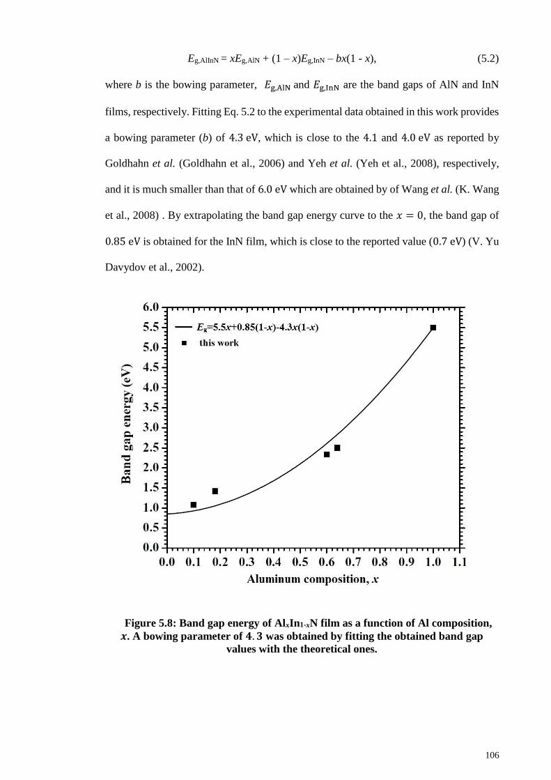
106
Eg,AlInN = xEg,AlN + (1 – x)Eg,InN – bx(1 - x), (5.2)
where b is the bowing parameter, 𝐸g,AlN and 𝐸g,InN are the band gaps of AlN and InN
films, respectively. Fitting Eq. 5.2 to the experimental data obtained in this work provides
a bowing parameter (b) of 4.3 eV, which is close to the 4.1 and 4.0 eV as reported by
Goldhahn et al. (Goldhahn et al., 2006) and Yeh et al. (Yeh et al., 2008), respectively,
and it is much smaller than that of 6.0 eV which are obtained by of Wang et al. (K. Wang
et al., 2008) . By extrapolating the band gap energy curve to the 𝑥 = 0, the band gap of
0.85 eV is obtained for the InN film, which is close to the reported value (0.7 eV) (V. Yu
Davydov et al., 2002).
Figure 5.8: Band gap energy of AlxIn1-xN film as a function of Al composition,
𝒙. A bowing parameter of 𝟒. 𝟑 was obtained by fitting the obtained band gap
values with the theoretical ones.
107
5.3 Effects of Nitrogen Flow Rate on Structure, Morphology, Composition and
Optical Properties of In-rich and Al-rich Aluminum Indium Nitride Thin
Films
The previous study on the effects of VIn on the aluminum composition of the AlxIn1-
xN thin films showed that they can be categorized into two groups: In-rich (with x = 0.1
and 0.18) and Al-rich films (with x = 0.6 and 0.64). For the study on the effects of N2
flow rate on the properties of the films, a sample from each category of these films was
employed.
XPS analysis was performed to investigate the Al (In) mole fraction in the as-prepared
In-rich (on quartz) and Al-rich (on Si(111)) AlxIn1-xN films. Figure 5.9 and 5.10 show the
In3d5/2 core-level photoelectron spectra of the In-rich and Al-rich films, respectively
deposited at various N2 flow rates. The core-level photoelectron spectra of the AlxIn1-xN
films were deconvoluted into three main sub-peaks centered at 445.4 ± 0.1, 444.4 ±
0.1 and 443.5 ± 0.1 eV, which are attributed to In−O, In−N and In−In bonds,
respectively (A. K. S. Chauhan et al., 2015; Lebedev et al., 2006). The corresponding
Al2p core-level photoelectron spectra of the films are presented in the insets of Figures
5.9 and 5.10. The spectra were deconvoluted into two main components at 75.2 ± 0.2
and 74.25 ± 0.1 eV assigned to Al−O and Al−N bonds, respectively (Rosenberger et
al., 2008; You et al., 2013). In addition, the Al2p core-level photoelectron spectra of some
deposited films exhibit a minor bump at the lower bonding energy side (72.8 ± 0.1 eV),
which corresponds to the Al−Al bonding within the films (Rosenberger et al., 2008).
The estimated Al mole fractions (x) in the In-rich AlxIn1-xN films were determined to
be 0.11, 0.07, 0.05 and 0.03 for the films deposited at the nitrogen flow rates of 40, 60,
80 and 100, respectively. The corresponding x values for the Al-rich AlxIn1-xN thin films
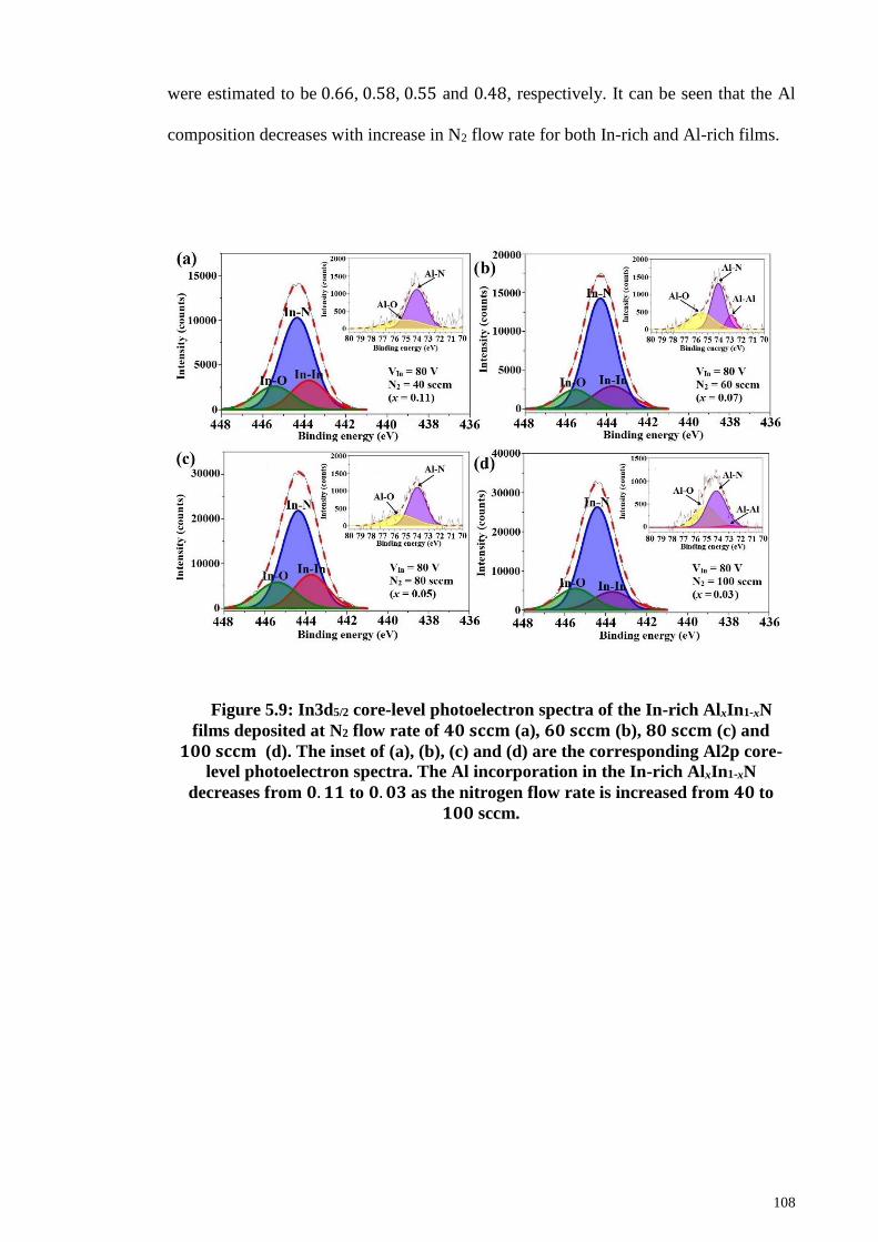
108
were estimated to be 0.66, 0.58, 0.55 and 0.48, respectively. It can be seen that the Al
composition decreases with increase in N2 flow rate for both In-rich and Al-rich films.
Figure 5.9: In3d5/2 core-level photoelectron spectra of the In-rich AlxIn1-xN
films deposited at N2 flow rate of 𝟒𝟎 𝐬𝐜𝐜𝐦 (a), 𝟔𝟎 𝐬𝐜𝐜𝐦 (b), 𝟖𝟎 𝐬𝐜𝐜𝐦 (c) and
𝟏𝟎𝟎 𝐬𝐜𝐜𝐦 (d). The inset of (a), (b), (c) and (d) are the corresponding Al2p core-
level photoelectron spectra. The Al incorporation in the In-rich AlxIn1-xN
decreases from 𝟎. 𝟏𝟏 to 𝟎. 𝟎𝟑 as the nitrogen flow rate is increased from 𝟒𝟎 to
𝟏𝟎𝟎 sccm.
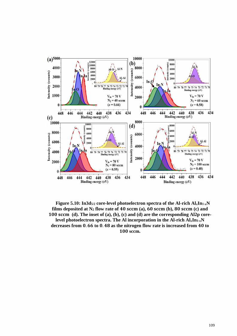
109
Figure 5.10: In3d5/2 core-level photoelectron spectra of the Al-rich AlxIn1-xN
films deposited at N2 flow rate of 𝟒𝟎 𝐬𝐜𝐜𝐦 (a), 𝟔𝟎 𝐬𝐜𝐜𝐦 (b), 𝟖𝟎 𝐬𝐜𝐜𝐦 (c) and
𝟏𝟎𝟎 𝐬𝐜𝐜𝐦 (d). The inset of (a), (b), (c) and (d) are the corresponding Al2p core-
level photoelectron spectra. The Al incorporation in the Al-rich AlxIn1-xN
decreases from 𝟎. 𝟔𝟔 to 𝟎. 𝟒𝟖 as the nitrogen flow rate is increased from 𝟒𝟎 to
𝟏𝟎𝟎 sccm.
110
The decrease in x as a result of increment in the flow rate of the nitrogen gas can be
explained in terms of plasma dynamics. By increasing the N2 flow rate, more excited
atoms are generated in the plasma and in the vicinity of the hot filament. The increase in
N2 flow rate also results in the presence of more unreacted hot N2 molecules in the vicinity
of the hot filament. More gas-phase reactions occur due to collisions between the excited
atoms and molecules. These reactions decrease the kinetic energy of ad-atoms/ions
impinging on the growth surface of the film resulting in the lower surface temperature
and decreasing their mobility. The bonding energy of Al−N bonds is much larger than
that of In−N (Costales, Blanco, Martín Pendás, Kandalam, & Pandey, 2002). Therefore,
under a higher nitrogen flow rate ad-atoms/ions with lower energy are energetically
favorable for the formation of In−N, rather than Al−N bonds, resulting in a higher InN
presence in the AlxIn1-xN film’s structure compared to AlN.
Figures 5.11 and 5.12 show the N1s core-level photoelectron spectra of the In-rich
and Al-rich AlxIn1-xN films, respectively that were grown at various N2 flow rates. The
N1s core-level photoelectron spectra of all samples were deconvoluted into two main sub-
peaks centered at 396.1 ± 0.2 and 396.8 ± 0.2 eV which are assigned to the N−In
(Shinoda & Mutsukura, 2002) and N−Al (Kuang et al., 2012a) bonds, respectively. The
presence of N−In and N−Al components further confirms the growth of the AlxIn1-xN
films. The spectra also exhibit a broad bump at the higher bonding energy side (398.7 ±
0.3 eV) corresponding to N−Al−O bond within grain boundaries of the films (Ozgit,
Donmez, Alevli, & Biyikli, 2012) . This indicates that the unsatisfied bonds on AlN have
higher affinity for O atoms as-compared to those on InN.
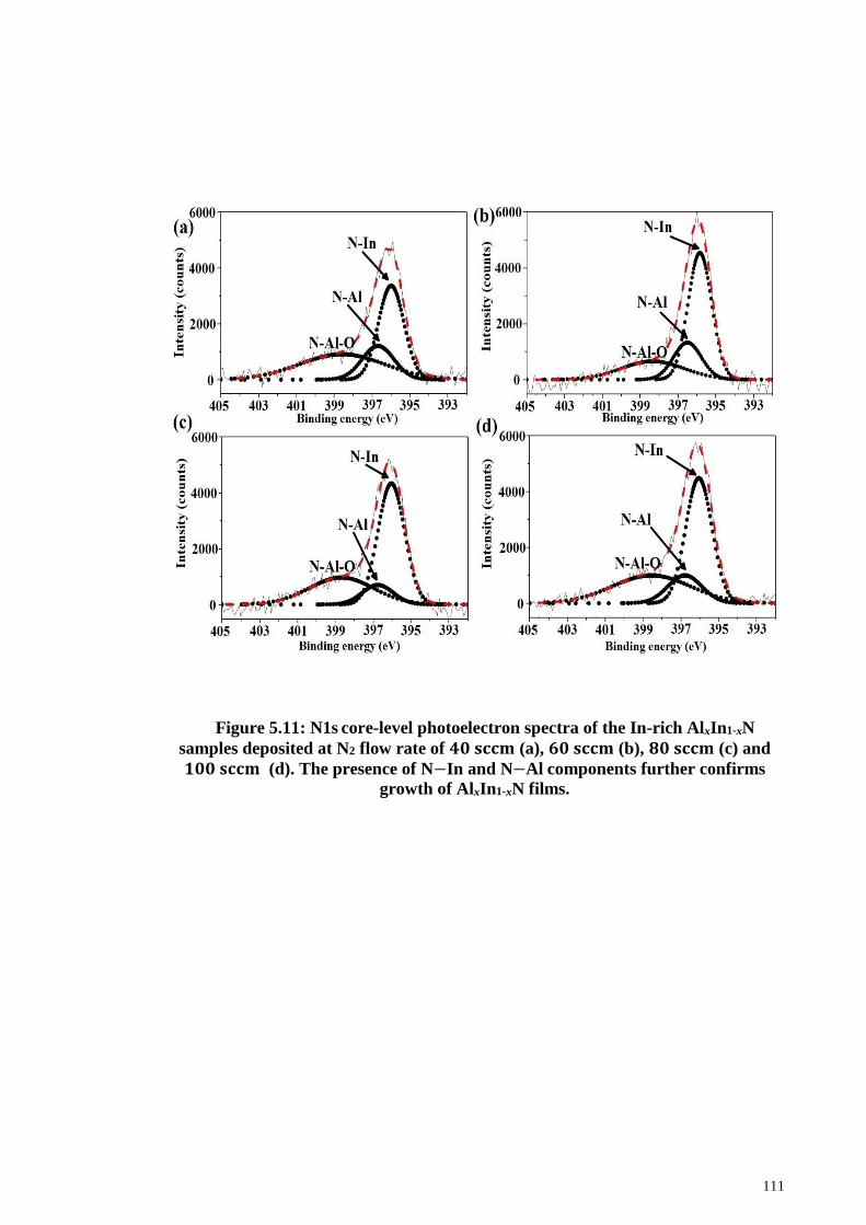
111
Figure 5.11: N1s core-level photoelectron spectra of the In-rich AlxIn1-xN
samples deposited at N2 flow rate of 𝟒𝟎 𝐬𝐜𝐜𝐦 (a), 𝟔𝟎 𝐬𝐜𝐜𝐦 (b), 𝟖𝟎 𝐬𝐜𝐜𝐦 (c) and
𝟏𝟎𝟎 𝐬𝐜𝐜𝐦 (d). The presence of N−In and N−Al components further confirms
growth of AlxIn1-xN films.
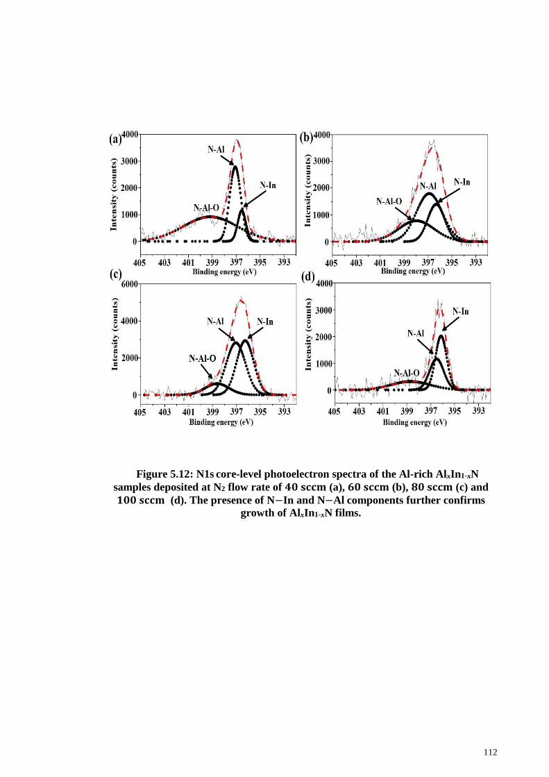
112
Figure 5.12: N1s core-level photoelectron spectra of the Al-rich AlxIn1-xN
samples deposited at N2 flow rate of 𝟒𝟎 𝐬𝐜𝐜𝐦 (a), 𝟔𝟎 𝐬𝐜𝐜𝐦 (b), 𝟖𝟎 𝐬𝐜𝐜𝐦 (c) and
𝟏𝟎𝟎 𝐬𝐜𝐜𝐦 (d). The presence of N−In and N−Al components further confirms
growth of AlxIn1-xN films.
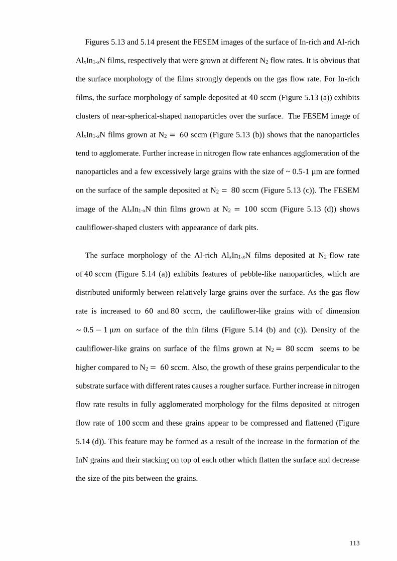
113
Figures 5.13 and 5.14 present the FESEM images of the surface of In-rich and Al-rich
AlxIn1-xN films, respectively that were grown at different N2 flow rates. It is obvious that
the surface morphology of the films strongly depends on the gas flow rate. For In-rich
films, the surface morphology of sample deposited at 40 sccm (Figure 5.13 (a)) exhibits
clusters of near-spherical-shaped nanoparticles over the surface. The FESEM image of
AlxIn1-xN films grown at N2 = 60 sccm (Figure 5.13 (b)) shows that the nanoparticles
tend to agglomerate. Further increase in nitrogen flow rate enhances agglomeration of the
nanoparticles and a few excessively large grains with the size of ~ 0.5-1 µm are formed
on the surface of the sample deposited at N2 = 80 sccm (Figure 5.13 (c)). The FESEM
image of the AlxIn1-xN thin films grown at N2 = 100 sccm (Figure 5.13 (d)) shows
cauliflower-shaped clusters with appearance of dark pits.
The surface morphology of the Al-rich AlxIn1-xN films deposited at N2 flow rate
of 40 sccm (Figure 5.14 (a)) exhibits features of pebble-like nanoparticles, which are
distributed uniformly between relatively large grains over the surface. As the gas flow
rate is increased to 60 and 80 sccm, the cauliflower-like grains with of dimension
~ 0.5 − 1 µ𝑚 on surface of the thin films (Figure 5.14 (b) and (c)). Density of the
cauliflower-like grains on surface of the films grown at N2 = 80 sccm seems to be
higher compared to N2 = 60 sccm. Also, the growth of these grains perpendicular to the
substrate surface with different rates causes a rougher surface. Further increase in nitrogen
flow rate results in fully agglomerated morphology for the films deposited at nitrogen
flow rate of 100 sccm and these grains appear to be compressed and flattened (Figure
5.14 (d)). This feature may be formed as a result of the increase in the formation of the
InN grains and their stacking on top of each other which flatten the surface and decrease
the size of the pits between the grains.
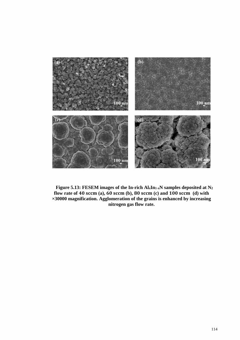
114
Figure 5.13: FESEM images of the In-rich AlxIn1-xN samples deposited at N2
flow rate of 𝟒𝟎 𝐬𝐜𝐜𝐦 (a), 𝟔𝟎 𝐬𝐜𝐜𝐦 (b), 𝟖𝟎 𝐬𝐜𝐜𝐦 (c) and 𝟏𝟎𝟎 𝐬𝐜𝐜𝐦 (d) with
×30000 magnification. Agglomeration of the grains is enhanced by increasing
nitrogen gas flow rate.
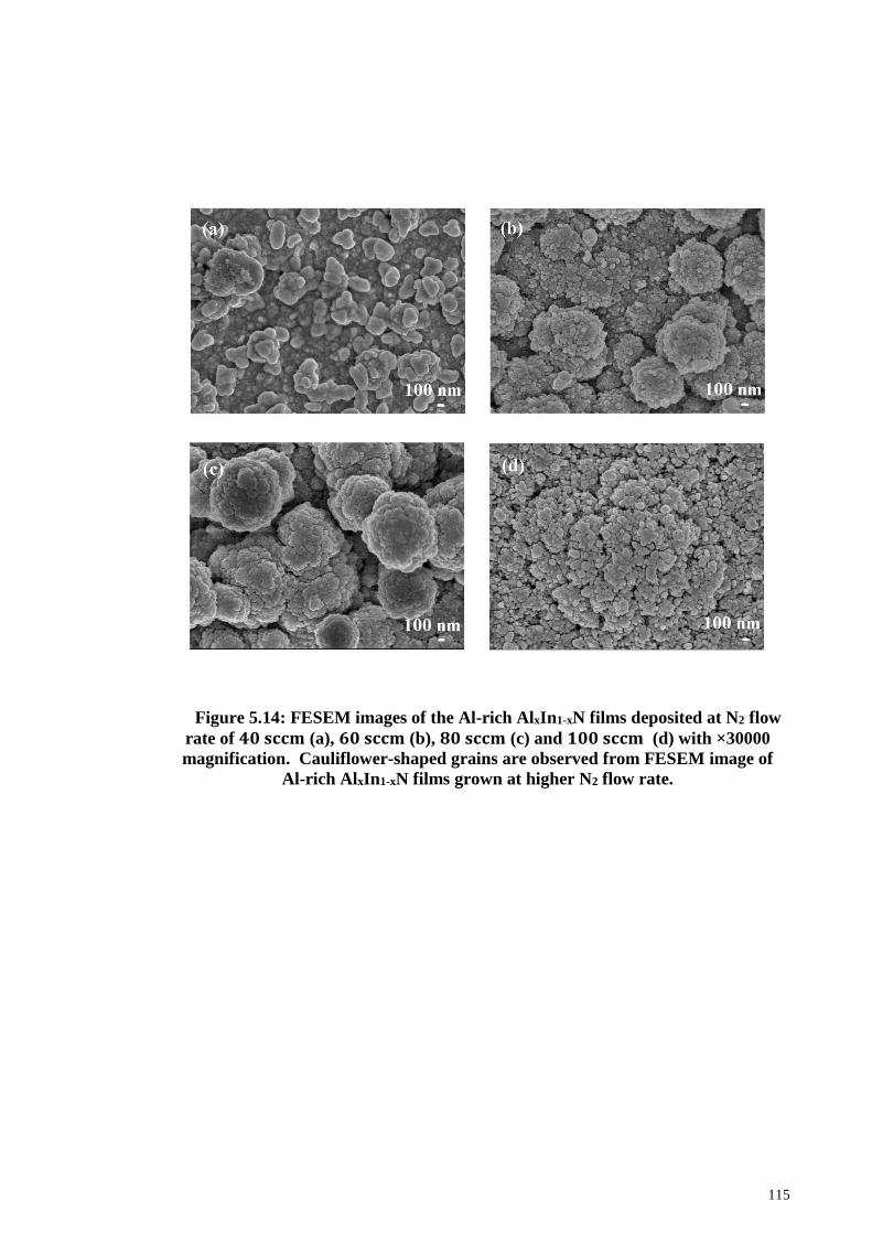
115
Figure 5.14: FESEM images of the Al-rich AlxIn1-xN films deposited at N2 flow
rate of 𝟒𝟎 𝐬𝐜𝐜𝐦 (a), 𝟔𝟎 𝐬𝐜𝐜𝐦 (b), 𝟖𝟎 𝐬𝐜𝐜𝐦 (c) and 𝟏𝟎𝟎 𝐬𝐜𝐜𝐦 (d) with ×30000
magnification. Cauliflower-shaped grains are observed from FESEM image of
Al-rich AlxIn1-xN films grown at higher N2 flow rate.
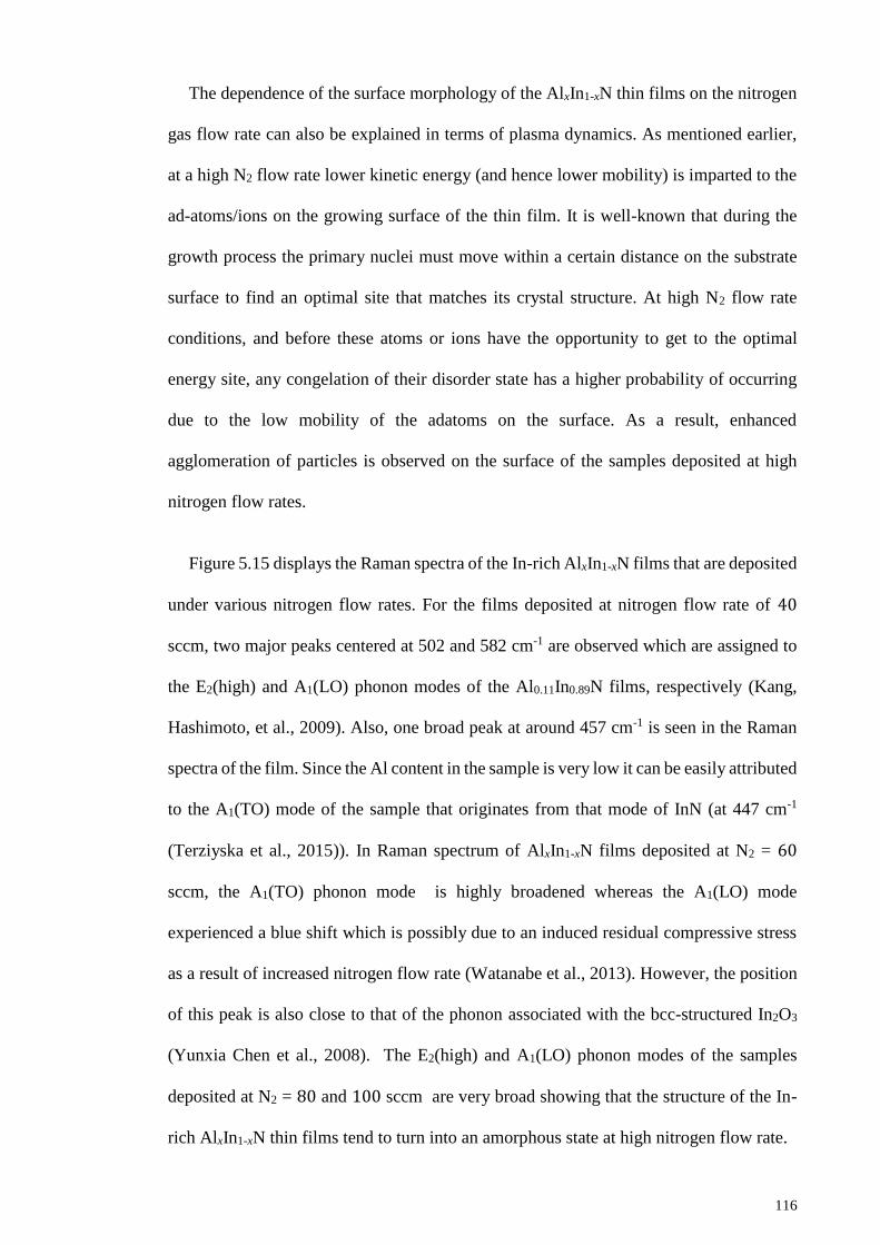
116
The dependence of the surface morphology of the AlxIn1-xN thin films on the nitrogen
gas flow rate can also be explained in terms of plasma dynamics. As mentioned earlier,
at a high N2 flow rate lower kinetic energy (and hence lower mobility) is imparted to the
ad-atoms/ions on the growing surface of the thin film. It is well-known that during the
growth process the primary nuclei must move within a certain distance on the substrate
surface to find an optimal site that matches its crystal structure. At high N2 flow rate
conditions, and before these atoms or ions have the opportunity to get to the optimal
energy site, any congelation of their disorder state has a higher probability of occurring
due to the low mobility of the adatoms on the surface. As a result, enhanced
agglomeration of particles is observed on the surface of the samples deposited at high
nitrogen flow rates.
Figure 5.15 displays the Raman spectra of the In-rich AlxIn1-xN films that are deposited
under various nitrogen flow rates. For the films deposited at nitrogen flow rate of 40
sccm, two major peaks centered at 502 and 582 cm-1 are observed which are assigned to
the E2(high) and A1(LO) phonon modes of the Al0.11In0.89N films, respectively (Kang,
Hashimoto, et al., 2009). Also, one broad peak at around 457 cm-1 is seen in the Raman
spectra of the film. Since the Al content in the sample is very low it can be easily attributed
to the A1(TO) mode of the sample that originates from that mode of InN (at 447 cm-1
(Terziyska et al., 2015)). In Raman spectrum of AlxIn1-xN films deposited at N2 = 60
sccm, the A1(TO) phonon mode is highly broadened whereas the A1(LO) mode
experienced a blue shift which is possibly due to an induced residual compressive stress
as a result of increased nitrogen flow rate (Watanabe et al., 2013). However, the position
of this peak is also close to that of the phonon associated with the bcc-structured In2O3
(Yunxia Chen et al., 2008). The E2(high) and A1(LO) phonon modes of the samples
deposited at N2 = 80 and 100 sccm are very broad showing that the structure of the In-
rich AlxIn1-xN thin films tend to turn into an amorphous state at high nitrogen flow rate.
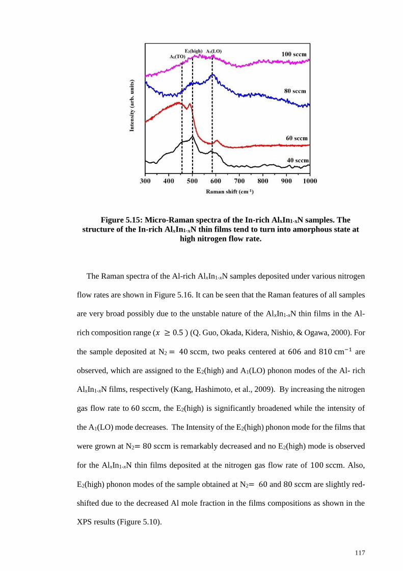
117
Figure 5.15: Micro-Raman spectra of the In-rich AlxIn1-xN samples. The
structure of the In-rich AlxIn1-xN thin films tend to turn into amorphous state at
high nitrogen flow rate.
The Raman spectra of the Al-rich AlxIn1-xN samples deposited under various nitrogen
flow rates are shown in Figure 5.16. It can be seen that the Raman features of all samples
are very broad possibly due to the unstable nature of the AlxIn1-xN thin films in the Al-
rich composition range (𝑥 ≥ 0.5 ) (Q. Guo, Okada, Kidera, Nishio, & Ogawa, 2000). For
the sample deposited at N2 = 40 sccm, two peaks centered at 606 and 810 cm−1 are
observed, which are assigned to the E2(high) and A1(LO) phonon modes of the Al- rich
AlxIn1-xN films, respectively (Kang, Hashimoto, et al., 2009). By increasing the nitrogen
gas flow rate to 60 sccm, the E2(high) is significantly broadened while the intensity of
the A1(LO) mode decreases. The Intensity of the E2(high) phonon mode for the films that
were grown at N2= 80 sccm is remarkably decreased and no E2(high) mode is observed
for the AlxIn1-xN thin films deposited at the nitrogen gas flow rate of 100 sccm. Also,
E2(high) phonon modes of the sample obtained at N2= 60 and 80 sccm are slightly red-
shifted due to the decreased Al mole fraction in the films compositions as shown in the
XPS results (Figure 5.10).
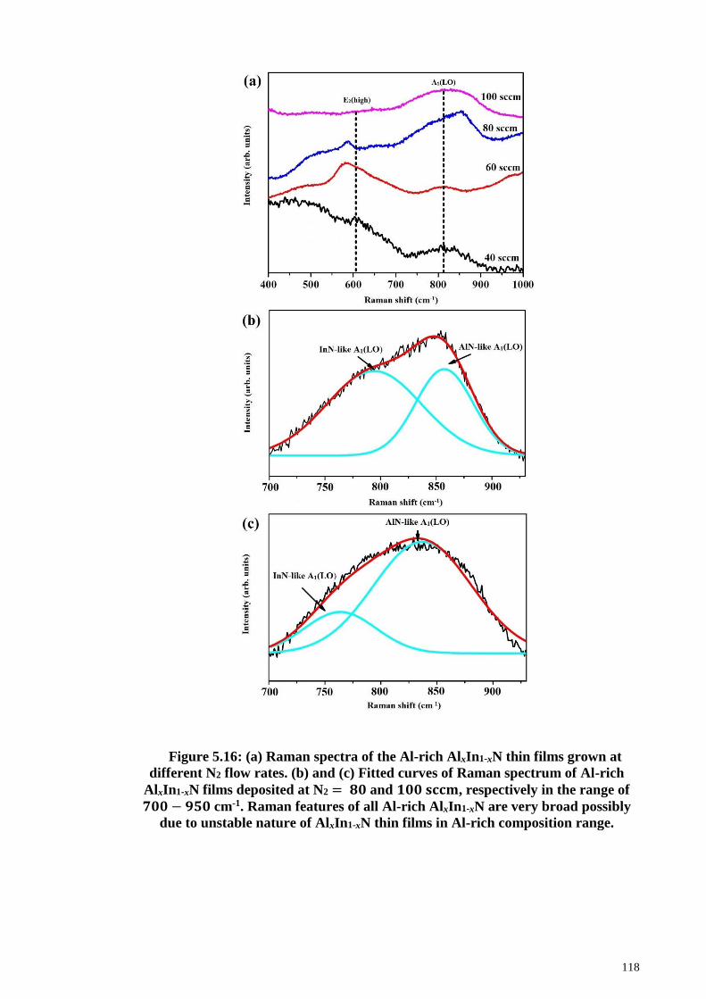
118
Figure 5.16: (a) Raman spectra of the Al-rich AlxIn1-xN thin films grown at
different N2 flow rates. (b) and (c) Fitted curves of Raman spectrum of Al-rich
AlxIn1-xN films deposited at N2 = 𝟖𝟎 and 𝟏𝟎𝟎 𝐬𝐜𝐜𝐦, respectively in the range of
𝟕𝟎𝟎 − 𝟗𝟓𝟎 cm-1. Raman features of all Al-rich AlxIn1-xN are very broad possibly
due to unstable nature of AlxIn1-xN thin films in Al-rich composition range.
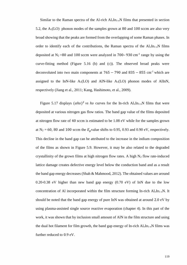
119
Similar to the Raman spectra of the Al-rich AlxIn1-xN films that presented in section
5.2, the A1(LO) phonon modes of the samples grown at 80 and 100 sccm are also very
broad showing that the peaks are formed from the overlapping of some Raman phases. In
order to identify each of the contributions, the Raman spectra of the AlxIn1-xN films
deposited at N2 =80 and 100 sccm were analyzed in 700– 930 cm-1 range by using the
curve-fitting method (Figure 5.16 (b) and (c)). The observed broad peaks were
deconvoluted into two main components at 765 − 790 and 835 − 855 cm-1 which are
assigned to the InN-like A1(LO) and AlN-like A1(LO) phonon modes of AlInN,
respectively (Jiang et al., 2011; Kang, Hashimoto, et al., 2009).
Figure 5.17 displays (𝛼ℎ𝜐)2 vs ℎ𝜐 curves for the In-rich AlxIn1-xN films that were
deposited at various nitrogen gas flow ratios. The band gap value of the films deposited
at nitrogen flow rate of 40 sccm is estimated to be 1.08 eV while for the samples grown
at N2 = 60, 80 and 100 sccm the 𝐸𝑔value shifts to 0.95, 0.93 and 0.90 eV, respectively.
This decline in the band gap can be attributed to the increase in the indium composition
of the films as shown in Figure 5.9. However, it may be also related to the degraded
crystallinity of the grown films at high nitrogen flow rates. A high N2 flow rate-induced
lattice damage creates defective energy level below the conduction band and as a result
the band gap energy decreases (Shah & Mahmood, 2012). The obtained values are around
0.20-0.38 eV higher than new band gap energy (0.70 eV) of InN due to the low
concentration of Al incorporated within the film structure forming In-rich AlxIn1-xN. It
should be noted that the band gap energy of pure InN was obtained at around 2.0 eV by
using plasma-assisted single source reactive evaporation (chapter 4). In this part of the
work, it was shown that by inclusion small amount of AlN in the film structure and using
the dual hot filament for film growth, the band gap energy of In-rich AlxIn1-xN films was
further reduced to 0.9 eV.
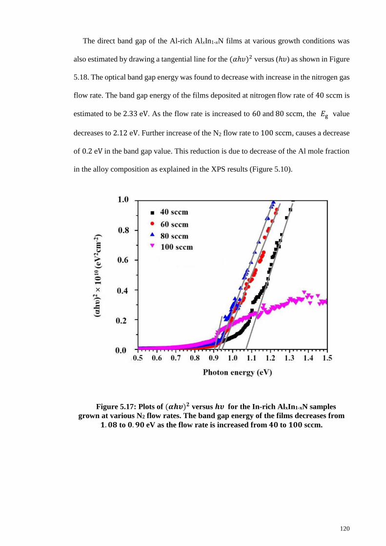
120
The direct band gap of the Al-rich AlxIn1-xN films at various growth conditions was
also estimated by drawing a tangential line for the (𝛼ℎ𝜐)2 versus (ℎ𝜐) as shown in Figure
5.18. The optical band gap energy was found to decrease with increase in the nitrogen gas
flow rate. The band gap energy of the films deposited at nitrogen flow rate of 40 sccm is
estimated to be 2.33 eV. As the flow rate is increased to 60 and 80 sccm, the 𝐸g value
decreases to 2.12 eV. Further increase of the N2 flow rate to 100 sccm, causes a decrease
of 0.2 eV in the band gap value. This reduction is due to decrease of the Al mole fraction
in the alloy composition as explained in the XPS results (Figure 5.10).
Figure 5.17: Plots of (𝜶𝒉𝝊)𝟐 versus 𝒉𝝊 for the In-rich AlxIn1-xN samples
grown at various N2 flow rates. The band gap energy of the films decreases from
𝟏. 𝟎𝟖 to 𝟎. 𝟗𝟎 eV as the flow rate is increased from 𝟒𝟎 to 𝟏𝟎𝟎 sccm.
121
Figure 5.18: Plots of (𝜶𝒉𝝊)𝟐 versus 𝒉𝝊 for Al-rich AlxIn1-xN films grown at
different N2 flow rates. The band gap energy of the films decreases from 𝟐. 𝟑𝟑 to
𝟏. 𝟗𝟐 eV as the flow rate is increased from 𝟒𝟎 to 𝟏𝟎𝟎 sccm.
5.4 Effects of Annealing Temperature on the Composition, Structure and
Optical Properties of Aluminum Indium Nitride Thin Films
Figure 5.19 (a)-(e) shows the In3d5/2 core-level photoelectron spectra of the as-grown
In-rich AlxIn1-xN films and the films annealed at various temperatures. As mentioned
earlier, the core-level photoelectron spectrum of the as-grown AlxIn1-xN films (Figure
5.19 (a)) was deconvoluted into three main sub-peaks centered at 445.5, 444.4 and
443.6 eV, which are attributed to In−O, In−N and In−In bonds, respectively (A. K. S.
Chauhan et al., 2015; Lebedev et al., 2006). The exact positions with minimum error were
applied for the deconvolution of rest of the spectra, to examine them more accurately. It
can be clearly seen that for all annealed samples, only In−O and In−N are observed. This
is possibly due to high affinity of the metallic indium to the remnant oxygen from the
122
annealing tube and/or bond transformation of In−In to In−O. At low annealing
temperatures (e.g., 200 and 300 °C) the intensity of the In−N bond is higher showing
that the InN formation is still dominant (Figure 5.19 (b) and (c)). However, by increasing
the annealing temperature to 400 and 500 °C (Figure 5.19 (d) and (e)), the intensity of
the In−N bond decreases dramatically while the intensity of the In−O bond becomes
increasingly dominant. This may be attributed to dissociation of the In−N bonds followed
by the oxidation of the metallic indium. Hence, the elemental compositional studies on
the annealed films showed that low-temperature (e.g., ≤300 °C) environments should be
considered for the application of these AlxIn1-xN films grown by the plasma-assisted
reactive evaporation in the devices.
In order to further investigate the stability of the films, the N1s core-level
photoelectron spectra of the as-grown and annealed samples were also analyzed (Figure
5.20 (a)-(e)). The N1s core-level photoelectron spectrum of the as-grown (Figure 5.20
(a)) sample was deconvoluted into three main sub-peaks centered at 396, 396.7 and
398.5 eV, which are assigned to N−In, N−Al and N−Al−O bonds, respectively (Kuang
et al., 2012a; Ozgit et al., 2012; Shinoda & Mutsukura, 2002). After the annealing process,
the N1s spectra of all the samples were eliminated and only the N−In and N−Al−O
components are observed from the fitted spectra (Figure 5.20 (b)-(e)). By increasing the
annealing temperature from 200 to 500 °C, the intensity of N−In decreases dramatically
reflecting the fact that the prepared alloys are unstable at high-temperature environment.
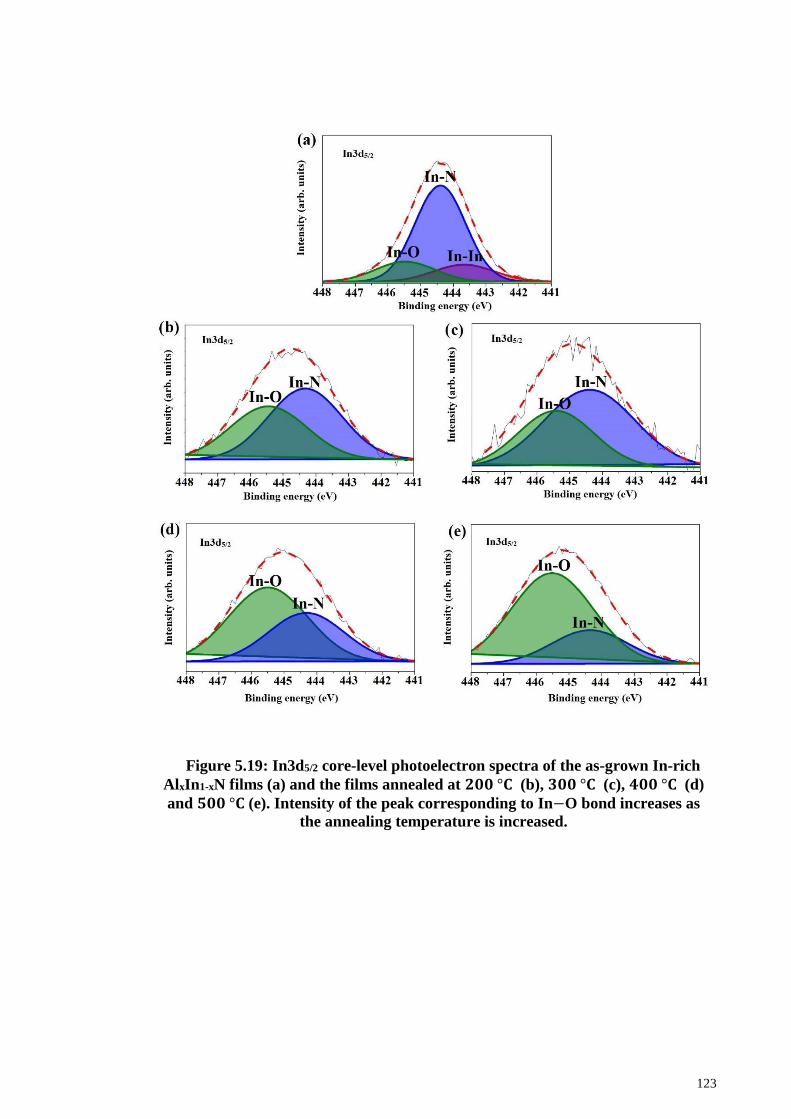
123
Figure 5.19: In3d5/2 core-level photoelectron spectra of the as-grown In-rich
AlxIn1-xN films (a) and the films annealed at 𝟐𝟎𝟎 °𝐂 (b), 𝟑𝟎𝟎 °𝐂 (c), 𝟒𝟎𝟎 °𝐂 (d)
and 𝟓𝟎𝟎 °𝐂 (e). Intensity of the peak corresponding to In−O bond increases as
the annealing temperature is increased.
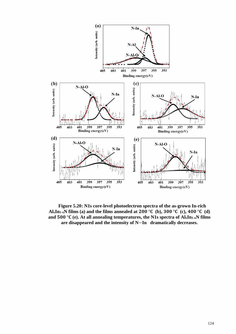
124
Figure 5.20: N1s core-level photoelectron spectra of the as-grown In-rich
AlxIn1-xN films (a) and the films annealed at 𝟐𝟎𝟎 °𝐂 (b), 𝟑𝟎𝟎 °𝐂 (c), 𝟒𝟎𝟎 °𝐂 (d)
and 𝟓𝟎𝟎 °𝐂 (e). At all annealing temperatures, the N1s spectra of AlxIn1-xN films
are disappeared and the intensity of N−In dramatically decreases.
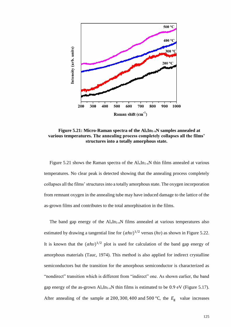
125
Figure 5.21: Micro-Raman spectra of the AlxIn1-xN samples annealed at
various temperatures. The annealing process completely collapses all the films’
structures into a totally amorphous state.
Figure 5.21 shows the Raman spectra of the AlxIn1-xN thin films annealed at various
temperatures. No clear peak is detected showing that the annealing process completely
collapses all the films’ structures into a totally amorphous state. The oxygen incorporation
from remnant oxygen in the annealing tube may have induced damage to the lattice of the
as-grown films and contributes to the total amorphisation in the films.
The band gap energy of the AlxIn1-xN films annealed at various temperatures also
estimated by drawing a tangential line for (𝛼ℎ𝜐)1/2 versus (ℎ𝜐) as shown in Figure 5.22.
It is known that the (𝛼ℎ𝜐)1/2 plot is used for calculation of the band gap energy of
amorphous materials (Tauc, 1974). This method is also applied for indirect crystalline
semiconductors but the transition for the amorphous semiconductor is characterized as
“nondirect” transition which is different from “indirect” one. As shown earlier, the band
gap energy of the as-grown AlxIn1-xN thin films is estimated to be 0.9 eV (Figure 5.17).
After annealing of the sample at 200, 300, 400 and 500 °C, the 𝐸g value increases
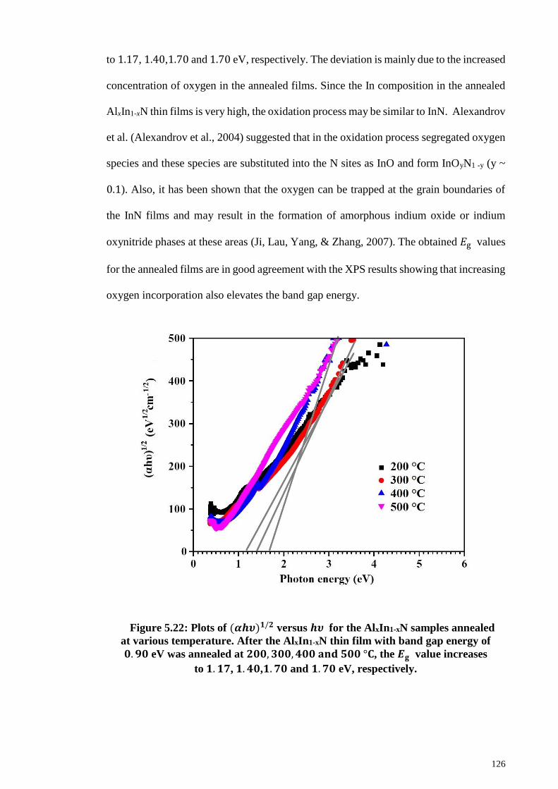
126
to 1.17, 1.40,1.70 and 1.70 eV, respectively. The deviation is mainly due to the increased
concentration of oxygen in the annealed films. Since the In composition in the annealed
AlxIn1-xN thin films is very high, the oxidation process may be similar to InN. Alexandrov
et al. (Alexandrov et al., 2004) suggested that in the oxidation process segregated oxygen
species and these species are substituted into the N sites as InO and form InOyN1 -y (y ~
0.1). Also, it has been shown that the oxygen can be trapped at the grain boundaries of
the InN films and may result in the formation of amorphous indium oxide or indium
oxynitride phases at these areas (Ji, Lau, Yang, & Zhang, 2007). The obtained 𝐸g values
for the annealed films are in good agreement with the XPS results showing that increasing
oxygen incorporation also elevates the band gap energy.
Figure 5.22: Plots of (𝜶𝒉𝝊)𝟏/𝟐 versus 𝒉𝝊 for the AlxIn1-xN samples annealed
at various temperature. After the AlxIn1-xN thin film with band gap energy of
𝟎. 𝟗𝟎 eV was annealed at 𝟐𝟎𝟎, 𝟑𝟎𝟎, 𝟒𝟎𝟎 𝐚𝐧𝐝 𝟓𝟎𝟎 °𝐂, the 𝑬𝐠 value increases
to 𝟏. 𝟏𝟕, 𝟏. 𝟒𝟎,𝟏. 𝟕𝟎 and 𝟏. 𝟕𝟎 eV, respectively.
127
5.5 Summary
In-rich (𝑥 = 0.10 and 0.18) and Al-rich (𝑥 = 0.60 and 0.64) AlxIn1-xN thin films were
successfully deposited by varying the voltage applied to the indium wire (VIn) in plasma-
assisted dual source reactive evaporation system. Raman results indicated that E2(high)
and A1(LO) peaks of the AlxIn1-xN films are considerably blue-shifted by decreasing
VIn and the A1(LO) phonon mode of the Al-rich films exhibits two-mode behavior.
Optical characterizations showed that the band gap energy of the films increased from
1.08 eV to 2.5 eV as the Al composition is varied from 0.1 to 0.64. A bowing parameter
of 4.3 eV was calculated for the grown AlxIn1-xN films and the extrapolated value from
the bowing equation was 0.85 eV for band gap energy of for InN. The effect of nitrogen
gas flow rate on the structural, morphological and optical properties of In-rich and Al-
rich AlxIn1-xN thin films was investigated. It was shown that Al incorporation (x) of both
In-rich and Al-rich AlxIn1-xN thin films decreases as the N2 flow rate is increased. FESEM
images of the AlxIn1-xN films reflects that by increasing the N2 flow rate agglomeration
of grains is enhanced. Optical characterizations showed that the band gap energy of the
In-rich and Al-rich films decreased by 0.18 eV and 0.41 eV, respectively, as the N2 flow
rate is increased from 40 to 100 sccm. Annealing studies shows that low-temperature
(e.g., ≤ 300 °C) environments should be considered for application of these AlxIn1-xN
films in the devices.
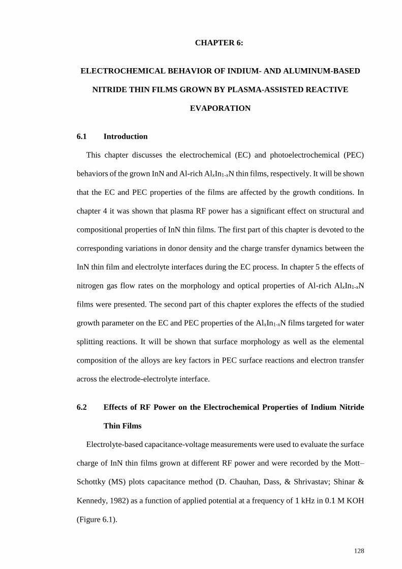
128
CHAPTER 6:
ELECTROCHEMICAL BEHAVIOR OF INDIUM- AND ALUMINUM-BASED
NITRIDE THIN FILMS GROWN BY PLASMA-ASSISTED REACTIVE
EVAPORATION
6.1 Introduction
This chapter discusses the electrochemical (EC) and photoelectrochemical (PEC)
behaviors of the grown InN and Al-rich AlxIn1-xN thin films, respectively. It will be shown
that the EC and PEC properties of the films are affected by the growth conditions. In
chapter 4 it was shown that plasma RF power has a significant effect on structural and
compositional properties of InN thin films. The first part of this chapter is devoted to the
corresponding variations in donor density and the charge transfer dynamics between the
InN thin film and electrolyte interfaces during the EC process. In chapter 5 the effects of
nitrogen gas flow rates on the morphology and optical properties of Al-rich AlxIn1-xN
films were presented. The second part of this chapter explores the effects of the studied
growth parameter on the EC and PEC properties of the AlxIn1-xN films targeted for water
splitting reactions. It will be shown that surface morphology as well as the elemental
composition of the alloys are key factors in PEC surface reactions and electron transfer
across the electrode-electrolyte interface.
6.2 Effects of RF Power on the Electrochemical Properties of Indium Nitride
Thin Films
Electrolyte-based capacitance-voltage measurements were used to evaluate the surface
charge of InN thin films grown at different RF power and were recorded by the Mott–
Schottky (MS) plots capacitance method (D. Chauhan, Dass, & Shrivastav; Shinar &
Kennedy, 1982) as a function of applied potential at a frequency of 1 kHz in 0.1 M KOH
(Figure 6.1).
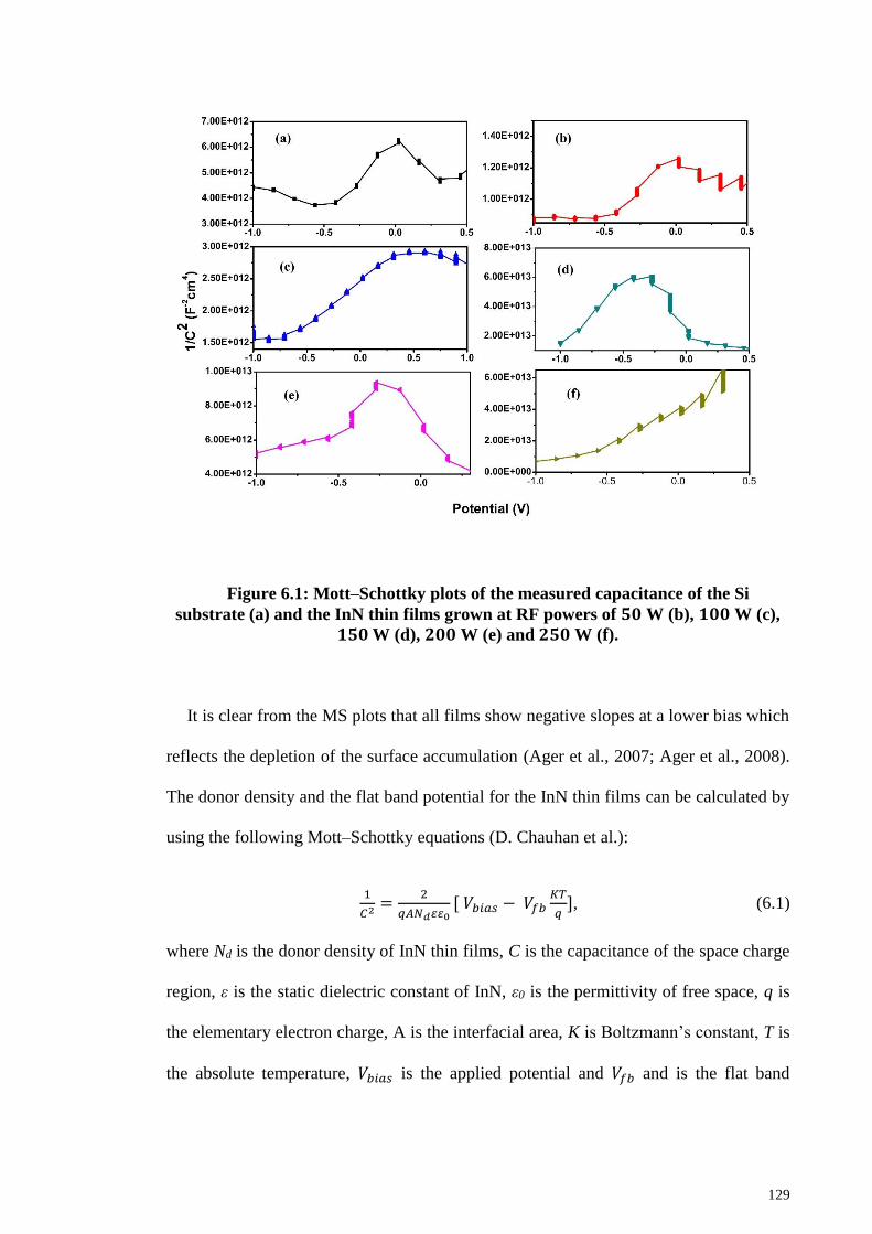
129
Figure 6.1: Mott–Schottky plots of the measured capacitance of the Si
substrate (a) and the InN thin films grown at RF powers of 𝟓𝟎 W (b), 𝟏𝟎𝟎 W (c),
𝟏𝟓𝟎 W (d), 𝟐𝟎𝟎 W (e) and 𝟐𝟓𝟎 W (f).
It is clear from the MS plots that all films show negative slopes at a lower bias which
reflects the depletion of the surface accumulation (Ager et al., 2007; Ager et al., 2008).
The donor density and the flat band potential for the InN thin films can be calculated by
using the following Mott–Schottky equations (D. Chauhan et al.):
1
𝐶2=
2
𝑞𝐴𝑁𝑑𝜀𝜀0[ 𝑉𝑏𝑖𝑎𝑠 − 𝑉𝑓𝑏
𝐾𝑇
𝑞], (6.1)
where Nd is the donor density of InN thin films, C is the capacitance of the space charge
region, ε is the static dielectric constant of InN, ε0 is the permittivity of free space, q is
the elementary electron charge, A is the interfacial area, K is Boltzmann’s constant, T is
the absolute temperature, 𝑉𝑏𝑖𝑎𝑠 is the applied potential and 𝑉𝑓𝑏 and is the flat band
130
potential. The 𝑁𝑑 of each InN thin films was calculated from slope of linear part of the
1 𝐶2⁄ curves vs. 𝑉𝑏𝑖𝑎𝑠 in equation (6-1):
Slope of ( 1
𝐶2) vs. (Vbias) =
2
𝑞𝐴𝑁𝑑 ℇℇ0. (6.2)
The 𝑉𝑓𝑏 of the InN films was estimated by drawing the linear part of 1 𝐶2⁄ curves
down to 𝑉𝑏𝑖𝑎𝑠 axis. The 𝑁𝑑 and 𝑉𝑓𝑏 of InN thin films that calculated from MS equations
were plotted as a function of the applied RF power in Figure 6.2. The Nd of the InN thin
film decreases steeply with the increase in RF power from 50 to 150 W but decreases
slowly with the increase in RF power to 200 W. This effect is due to the similar decreasing
trend in the oxygen atomic percentage in the film as shown in Figure 4.11. A further
increase in RF power to 250 W led to a slight increase in the oxygen concentrations
(Figure 4.11). As explained in chapter 4, the high RF power results in the sputtering of N
atoms from the growth surface. The energetic ions break up InN bonds and the unsatisfied
bonds left by the N atoms are replaced by the O atoms. This produces a slight increase in
donor concentration (from 1.1 × 10¹⁵ to 2.2 × 1015 cm-3).
As a matter of point, the EC properties of the grown thin films are attributed to
oxynitride phase with a large electron density that screens the underlying ions and inhibits
the oxidation reaction. Oxygen is the most common impurity and is mostly present on the
surface of the nitride films, thus resulting in free charge accumulations (F. Zhang et al.,
2012). The anodic current in the InN thin films deposited at lower RF power is larger due
to the improved charge separation at the semiconductor-electrolyte interface as a result of
higher presence of oxygen in the films composition. The 𝑉𝑓𝑏 of the InN thin films also
shows a similar trend with respect to RF power (Figure 6.2). Thus, it can be concluded
that the 𝑉𝑓𝑏 behavior is due to the presence of oxygen donor atoms in the film structure
which causes the band bending at the InN thin film/electrolyte interface.
131
Figure 6.2: Dependence of donor density (𝑵𝒅) and flat band potential (𝑽𝒇𝒃) of
the InN thin films on the applied RF power. At lower RF powers the 𝑵𝒅 of the
films is higher while the 𝑽𝒇𝒃 is more negative at higher RF power. (Note: The
lines joining the points are only used as a guide to the eye.).
The linear sweep voltammogram (LSV) of InN thin films were recorded in the
presence of 0.1 M KOH and the results are shown in Figure 6.3. It can be seen that, after
0 V, the anodic current increases with the increment of applied bias for all the InN thin
films. The bare Si substrate shows a negligible anodic current due to the absence of
electroactive species on the surface. By increasing RF power during the growth of InN
thin films from 50 to 200 W, the anodic current decreases. A further increase in the RF
power to 250 W results in a slight increase of the anodic current. This may be due to the
decrease in donor density in the InN thin film as a result of the increase in RF power as
(Figure 6.2). Hence, the observed anodic oxidation current is due to the oxygen evolution
reaction on the electrode surface in the presence of KOH (S. Chen & Qiao, 2013).
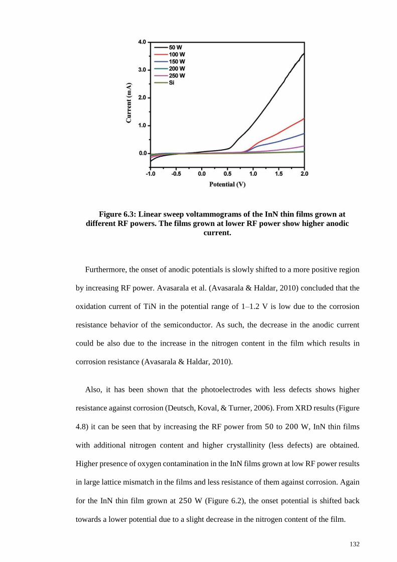
132
Figure 6.3: Linear sweep voltammograms of the InN thin films grown at
different RF powers. The films grown at lower RF power show higher anodic
current.
Furthermore, the onset of anodic potentials is slowly shifted to a more positive region
by increasing RF power. Avasarala et al. (Avasarala & Haldar, 2010) concluded that the
oxidation current of TiN in the potential range of 1–1.2 V is low due to the corrosion
resistance behavior of the semiconductor. As such, the decrease in the anodic current
could be also due to the increase in the nitrogen content in the film which results in
corrosion resistance (Avasarala & Haldar, 2010).
Also, it has been shown that the photoelectrodes with less defects shows higher
resistance against corrosion (Deutsch, Koval, & Turner, 2006). From XRD results (Figure
4.8) it can be seen that by increasing the RF power from 50 to 200 W, InN thin films
with additional nitrogen content and higher crystallinity (less defects) are obtained.
Higher presence of oxygen contamination in the InN films grown at low RF power results
in large lattice mismatch in the films and less resistance of them against corrosion. Again
for the InN thin film grown at 250 W (Figure 6.2), the onset potential is shifted back
towards a lower potential due to a slight decrease in the nitrogen content of the film.
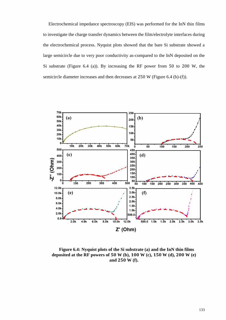
133
Electrochemical impedance spectroscopy (EIS) was performed for the InN thin films
to investigate the charge transfer dynamics between the film/electrolyte interfaces during
the electrochemical process. Nyquist plots showed that the bare Si substrate showed a
large semicircle due to very poor conductivity as-compared to the InN deposited on the
Si substrate (Figure 6.4 (a)). By increasing the RF power from 50 to 200 W, the
semicircle diameter increases and then decreases at 250 W (Figure 6.4 (b)-(f)).
Figure 6.4: Nyquist plots of the Si substrate (a) and the InN thin films
deposited at the RF powers of 𝟓𝟎 W (b), 𝟏𝟎𝟎 W (c), 𝟏𝟓𝟎 W (d), 𝟐𝟎𝟎 W (e)
and 𝟐𝟓𝟎 W (f).
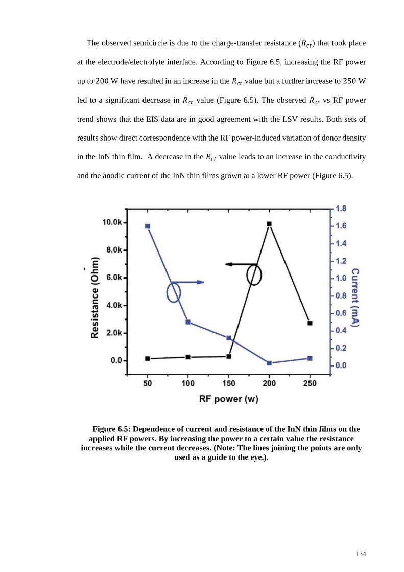
134
The observed semicircle is due to the charge-transfer resistance (𝑅𝑐𝑡) that took place
at the electrode/electrolyte interface. According to Figure 6.5, increasing the RF power
up to 200 W have resulted in an increase in the 𝑅𝑐𝑡 value but a further increase to 250 W
led to a significant decrease in 𝑅𝑐𝑡 value (Figure 6.5). The observed 𝑅𝑐𝑡 vs RF power
trend shows that the EIS data are in good agreement with the LSV results. Both sets of
results show direct correspondence with the RF power-induced variation of donor density
in the InN thin film. A decrease in the 𝑅𝑐𝑡 value leads to an increase in the conductivity
and the anodic current of the InN thin films grown at a lower RF power (Figure 6.5).
Figure 6.5: Dependence of current and resistance of the InN thin films on the
applied RF powers. By increasing the power to a certain value the resistance
increases while the current decreases. (Note: The lines joining the points are only
used as a guide to the eye.).
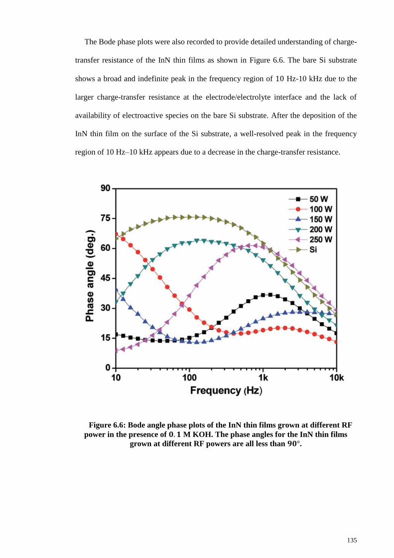
135
The Bode phase plots were also recorded to provide detailed understanding of charge-
transfer resistance of the InN thin films as shown in Figure 6.6. The bare Si substrate
shows a broad and indefinite peak in the frequency region of 10 Hz-10 kHz due to the
larger charge-transfer resistance at the electrode/electrolyte interface and the lack of
availability of electroactive species on the bare Si substrate. After the deposition of the
InN thin film on the surface of the Si substrate, a well-resolved peak in the frequency
region of 10 Hz–10 kHz appears due to a decrease in the charge-transfer resistance.
Figure 6.6: Bode angle phase plots of the InN thin films grown at different RF
power in the presence of 𝟎. 𝟏 M KOH. The phase angles for the InN thin films
grown at different RF powers are all less than 𝟗𝟎°.
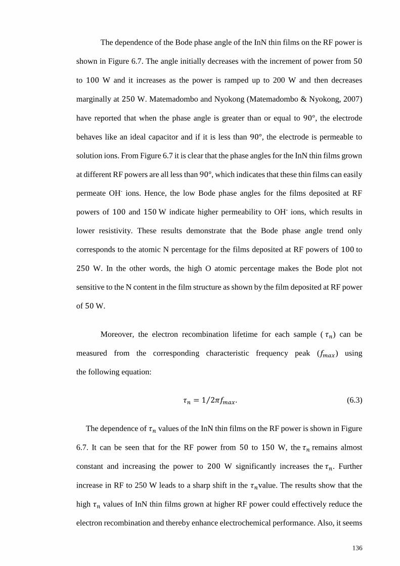
136
The dependence of the Bode phase angle of the InN thin films on the RF power is
shown in Figure 6.7. The angle initially decreases with the increment of power from 50
to 100 W and it increases as the power is ramped up to 200 W and then decreases
marginally at 250 W. Matemadombo and Nyokong (Matemadombo & Nyokong, 2007)
have reported that when the phase angle is greater than or equal to 90°, the electrode
behaves like an ideal capacitor and if it is less than 90°, the electrode is permeable to
solution ions. From Figure 6.7 it is clear that the phase angles for the InN thin films grown
at different RF powers are all less than 90°, which indicates that these thin films can easily
permeate OH- ions. Hence, the low Bode phase angles for the films deposited at RF
powers of 100 and 150 W indicate higher permeability to OH- ions, which results in
lower resistivity. These results demonstrate that the Bode phase angle trend only
corresponds to the atomic N percentage for the films deposited at RF powers of 100 to
250 W. In the other words, the high O atomic percentage makes the Bode plot not
sensitive to the N content in the film structure as shown by the film deposited at RF power
of 50 W.
Moreover, the electron recombination lifetime for each sample ( 𝜏𝑛) can be
measured from the corresponding characteristic frequency peak (𝑓𝑚𝑎𝑥) using
the following equation:
𝜏𝑛 = 1 2𝜋𝑓𝑚𝑎𝑥⁄ . (6.3)
The dependence of 𝜏𝑛 values of the InN thin films on the RF power is shown in Figure
6.7. It can be seen that for the RF power from 50 to 150 W, the 𝜏𝑛 remains almost
constant and increasing the power to 200 W significantly increases the 𝜏𝑛. Further
increase in RF to 250 W leads to a sharp shift in the 𝜏𝑛value. The results show that the
high 𝜏𝑛 values of InN thin films grown at higher RF power could effectively reduce the
electron recombination and thereby enhance electrochemical performance. Also, it seems
137
that the 𝜏𝑛 of the InN films deposited at various RF powers is independent of the N
percentage, conductivity and resistance of the films as different behaviors are observed
for these parameters at the various growth conditions.
Figure 6.7: Dependence of Bode phase angle and electron recombination
lifetime (𝝉𝒏) of the InN thin films on the applied RF powers. (Note: The lines
joining the points are only used as a guide to the eye.).
138
6.3 Electrochemical and Photoelectrochemical Behaviors of Aluminum Indium
Nitride Thin Films Grown by Plasma-Assisted Dual Source Reactive
Evaporation
The photoelectrochemical performance of the AlxIn1-xN thin films grown at various N2
flow rates was investigated for water splitting by using LSV techniques under simulated
solar AM 1.5 G irradiation in the presence of 0.1 M PBS (pH 7.2) at a scan rate of 50
mV/s. Figures 6.8(a) and (b) show the LSV of the samples in the absence and presence
of simulated solar irradiation, respectively. It can be seen that under both conditions, after
0 V, the anodic current increases with the increment in the applied bias for all the AlxIn1-
xN thin films. Also, by increasing the N2 flow rate from 40 to 80 sccm during the growth
of AlxIn1-xN thin films, the anodic current (in both dark and light conditions) significantly
increases and then decreases for the thin film grown at the N2 flow rate of 100 sccm.
The EC and PEC behaviors of the AlxIn1-xN thin films can be explained by taking into
account the dependence of the alloys morphology on N2 flow rate during the deposition
process. From Figure 5.14 it was observed that excessively large grains cover the whole
surface of the AlInN films deposited at N2 = 60 and 80 sccm. These large-sized grains
with porous morphology act as an effective channel for electron transfer, enhance surface
reaction rates and facilitate the interfacial electron transfer process due to the large
electrode-electrolyte interfacial contact area. This has been proven to be crucial for
improvement of the electronic interactions and interfacial electron transfer at the
electrode/electrolyte interface (Manivasakan, Ramasamy, & Kim, 2014).
More interestingly, Figure 6.8 (a) and (b) show that the anodic current significantly
increases when the simulated solar AM 1.5 G is illuminated onto the samples, especially
for those grown at nitrogen flow rates of 60 and 80 sccm. For instance, at 1.23 V the
current increases from 0.09 mA to 0.8 mA upon the AlxIn1-xN sample grown at N2 =
139
80 sccm being exposed to the light. This could be attributed to the band gap values and
the band alignments of AlxIn1-xN alloys with different Al(In) compositions which have
been reported to be crucial in photoelectrochemical water splitting reactions, as explained
in chapter 2. The results in Section 5.2 of this thesis showed that the films deposited at
the N2 flow rate of 60 and 80 sccm has a band gap energy of 2.12 eV and the Al
composition of 58% and 55%, respectively. The Al composition and band gap energy
values are consistent with the values reported by Collazo and Dietz (Ramón Collazo &
Dietz III, 2013), who showed that AlxIn1-xN with Al composition of ~55% possesses
suitable band alignment and band gap (2.2 eV) for photoelectrochemical water splitting.
They reported that at higher Al composition (e.g.,≥ 65%) the corresponding maximum
potential of the valence band is more positive whereas at lower Al composition (e.g.,≤
50% ) the band-edge potentials of the alloy do not properly straddle the H+/H2 and
O2/H2O redox potentials (Ramón Collazo & Dietz III, 2013). Hence, the photocurrent
enhancement of the AlxIn1-xN films deposited at N2 = 60 and 80 sccm could be due to the
composition and the band gap energy of the samples. The band alignment and band gap
of the films are similar to those of InxGa1-xN alloy with ~25% − 30% indium
composition which has been widely reported as an efficient photocatalyst material for
overall water splitting (AlOtaibi et al., 2013).
The time dependence of the photocurrent was measured for the AlxIn1-xN thin films
grown at nitrogen gas flow rate of 80 sccm under simulated AM 1.5 G illumination
(Figure 6.9). Measurements were also performed for the other films grown at the N2 flow
rates of 40, 60 and 100 sccm. No significant photo-response was observed for the films
grown at N2 flow rates of 40 and 100 sccm and the photo-response of the films grown at
N2 flow rate of 60 sccm (not shown here) was quite similar to that of the film grown at
N2 flow rate of 80 sccm.
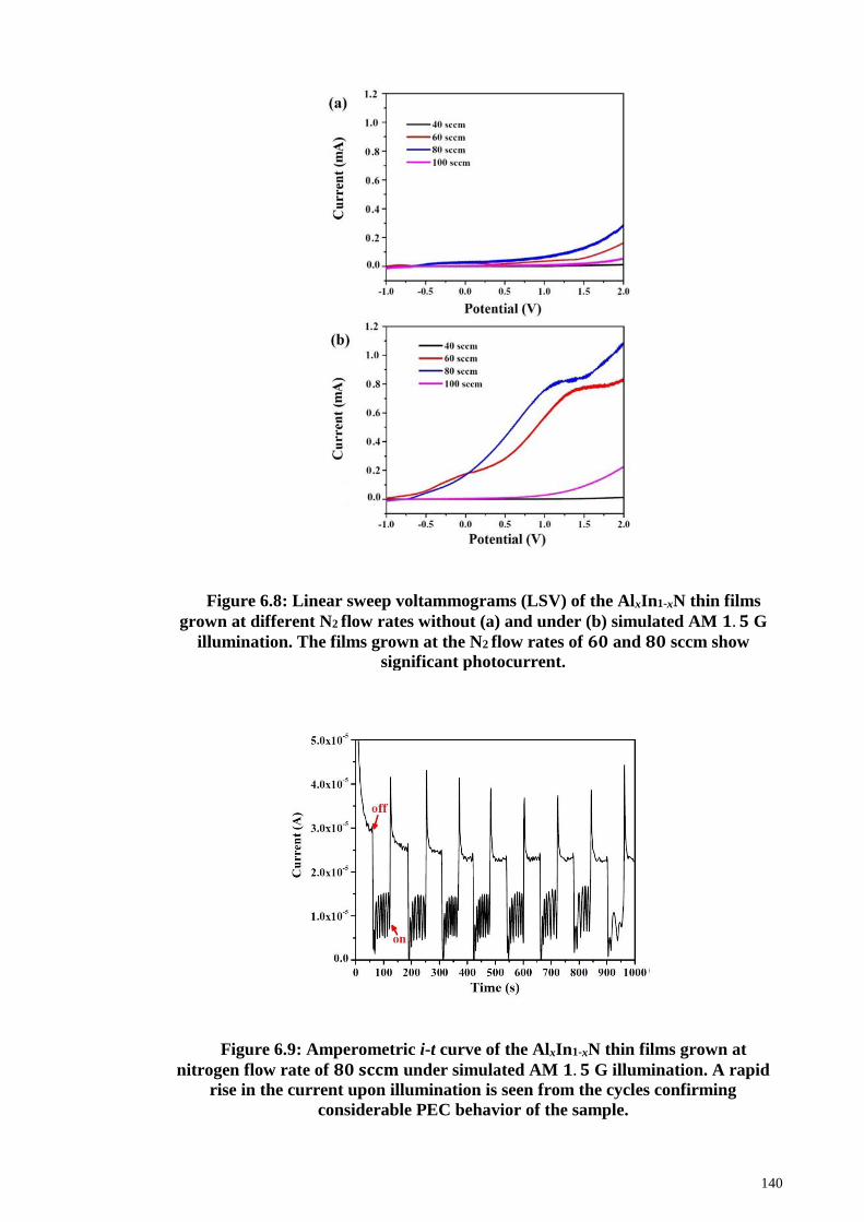
140
Figure 6.8: Linear sweep voltammograms (LSV) of the AlxIn1-xN thin films
grown at different N2 flow rates without (a) and under (b) simulated AM 𝟏. 𝟓 G
illumination. The films grown at the N2 flow rates of 𝟔𝟎 and 𝟖𝟎 sccm show
significant photocurrent.
Figure 6.9: Amperometric i-t curve of the AlxIn1-xN thin films grown at
nitrogen flow rate of 𝟖𝟎 𝐬𝐜𝐜𝐦 under simulated AM 𝟏. 𝟓 G illumination. A rapid
rise in the current upon illumination is seen from the cycles confirming
considerable PEC behavior of the sample.
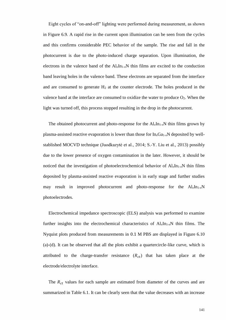
141
Eight cycles of “on-and-off” lighting were performed during measurement, as shown
in Figure 6.9. A rapid rise in the current upon illumination can be seen from the cycles
and this confirms considerable PEC behavior of the sample. The rise and fall in the
photocurrent is due to the photo-induced charge separation. Upon illumination, the
electrons in the valence band of the AlxIn1-xN thin films are excited to the conduction
band leaving holes in the valence band. These electrons are separated from the interface
and are consumed to generate H2 at the counter electrode. The holes produced in the
valence band at the interface are consumed to oxidize the water to produce O2. When the
light was turned off, this process stopped resulting in the drop in the photocurrent.
The obtained photocurrent and photo-response for the AlxIn1-xN thin films grown by
plasma-assisted reactive evaporation is lower than those for InxGa1-xN deposited by well-
stablished MOCVD technique (Juodkazytė et al., 2014; S.-Y. Liu et al., 2013) possibly
due to the lower presence of oxygen contamination in the later. However, it should be
noticed that the investigation of photoelectrochemical behavior of AlxIn1-xN thin films
deposited by plasma-assisted reactive evaporation is in early stage and further studies
may result in improved photocurrent and photo-response for the AlxIn1-xN
photoelectrodes.
Electrochemical impedance spectroscopic (ELS) analysis was performed to examine
further insights into the electrochemical characteristics of AlxIn1-xN thin films. The
Nyquist plots produced from measurements in 0.1 M PBS are displayed in Figure 6.10
(a)-(d). It can be observed that all the plots exhibit a quartercircle-like curve, which is
attributed to the charge-transfer resistance (𝑅𝑐𝑡) that has taken place at the
electrode/electrolyte interface.
The 𝑅𝑐𝑡 values for each sample are estimated from diameter of the curves and are
summarized in Table 6.1. It can be clearly seen that the value decreases with an increase
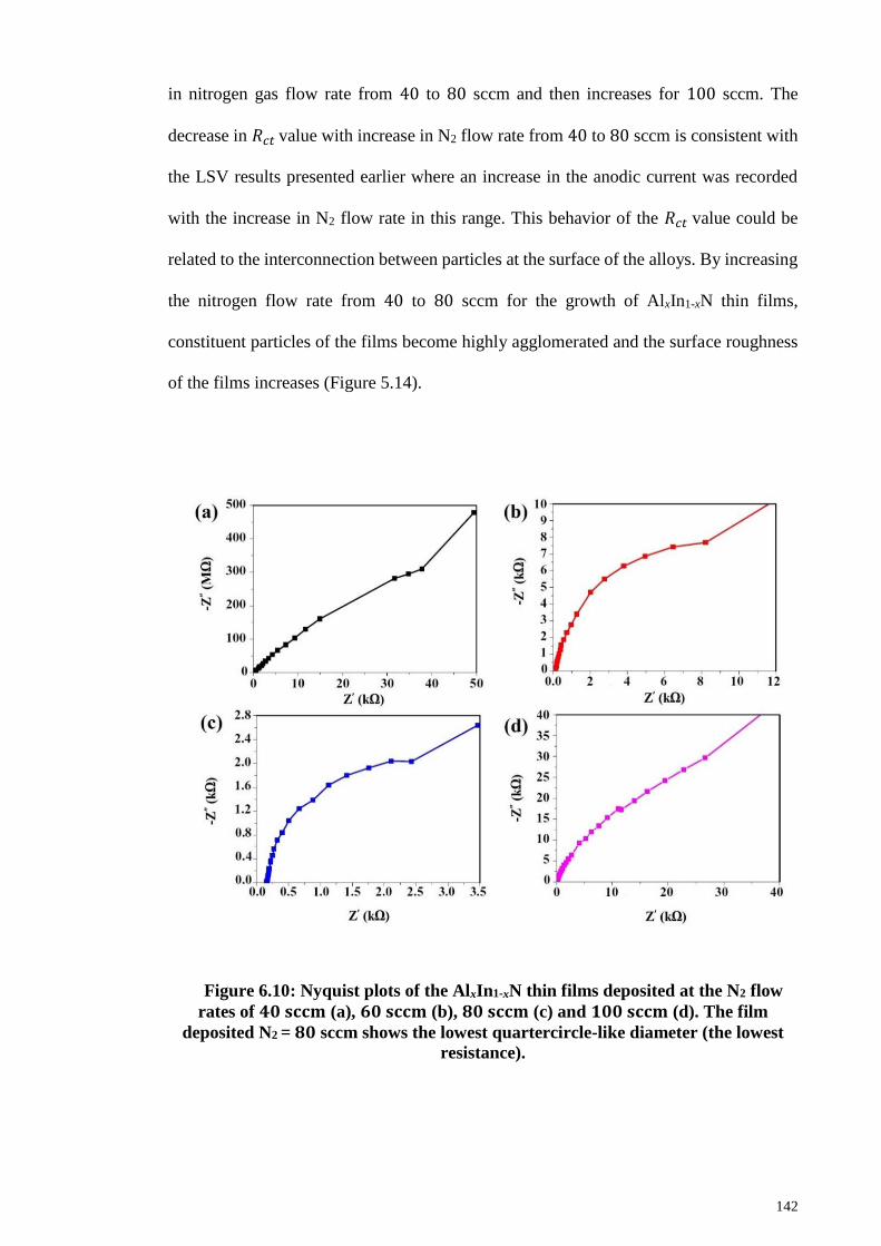
142
in nitrogen gas flow rate from 40 to 80 sccm and then increases for 100 sccm. The
decrease in 𝑅𝑐𝑡 value with increase in N2 flow rate from 40 to 80 sccm is consistent with
the LSV results presented earlier where an increase in the anodic current was recorded
with the increase in N2 flow rate in this range. This behavior of the 𝑅𝑐𝑡 value could be
related to the interconnection between particles at the surface of the alloys. By increasing
the nitrogen flow rate from 40 to 80 sccm for the growth of AlxIn1-xN thin films,
constituent particles of the films become highly agglomerated and the surface roughness
of the films increases (Figure 5.14).
Figure 6.10: Nyquist plots of the AlxIn1-xN thin films deposited at the N2 flow
rates of 𝟒𝟎 𝐬𝐜𝐜𝐦 (a), 𝟔𝟎 𝐬𝐜𝐜𝐦 (b), 𝟖𝟎 𝐬𝐜𝐜𝐦 (c) and 𝟏𝟎𝟎 𝐬𝐜𝐜𝐦 (d). The film
deposited N2 = 𝟖𝟎 sccm shows the lowest quartercircle-like diameter (the lowest
resistance).
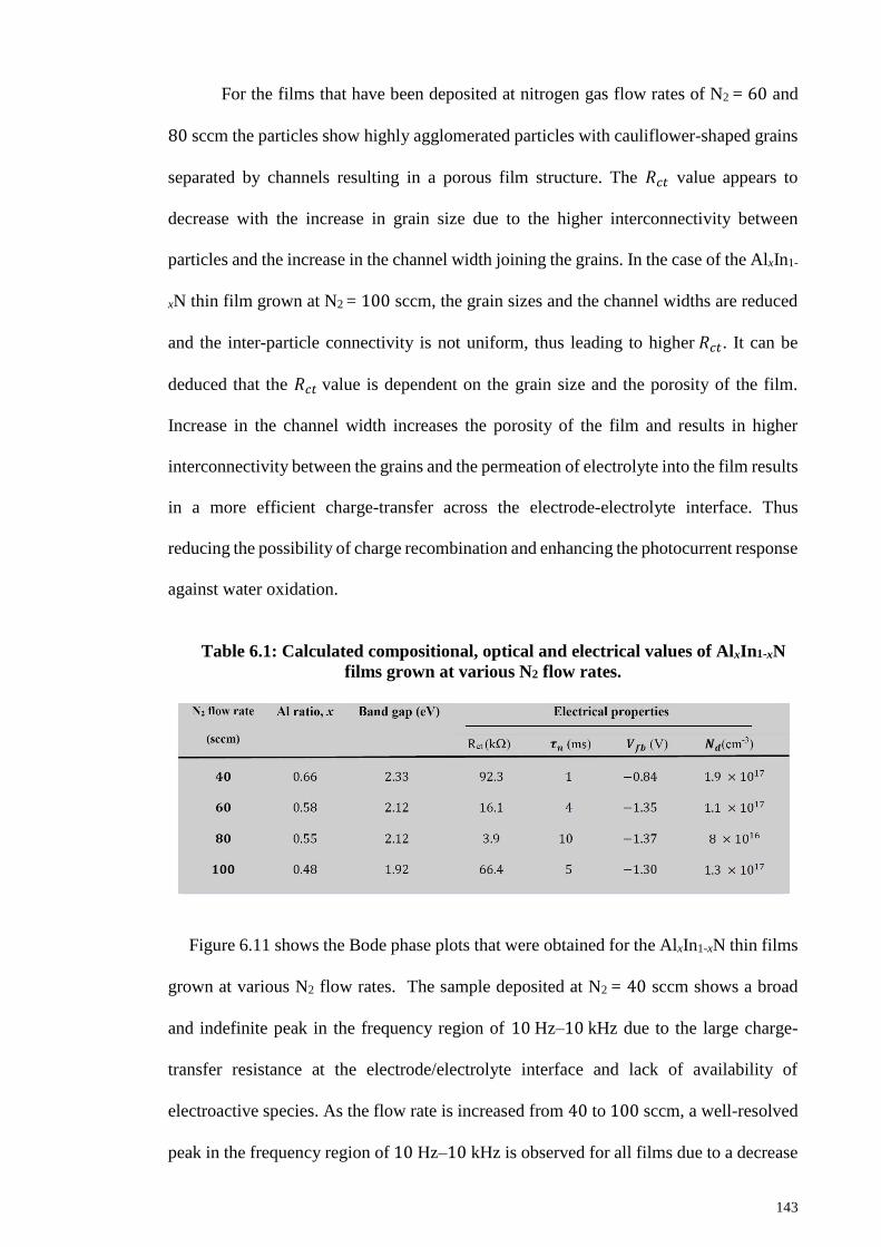
143
For the films that have been deposited at nitrogen gas flow rates of N2 = 60 and
80 sccm the particles show highly agglomerated particles with cauliflower-shaped grains
separated by channels resulting in a porous film structure. The 𝑅𝑐𝑡 value appears to
decrease with the increase in grain size due to the higher interconnectivity between
particles and the increase in the channel width joining the grains. In the case of the AlxIn1-
xN thin film grown at N2 = 100 sccm, the grain sizes and the channel widths are reduced
and the inter-particle connectivity is not uniform, thus leading to higher 𝑅𝑐𝑡. It can be
deduced that the 𝑅𝑐𝑡 value is dependent on the grain size and the porosity of the film.
Increase in the channel width increases the porosity of the film and results in higher
interconnectivity between the grains and the permeation of electrolyte into the film results
in a more efficient charge-transfer across the electrode-electrolyte interface. Thus
reducing the possibility of charge recombination and enhancing the photocurrent response
against water oxidation.
Table 6.1: Calculated compositional, optical and electrical values of AlxIn1-xN
films grown at various N2 flow rates.
Figure 6.11 shows the Bode phase plots that were obtained for the AlxIn1-xN thin films
grown at various N2 flow rates. The sample deposited at N2 = 40 sccm shows a broad
and indefinite peak in the frequency region of 10 Hz–10 kHz due to the large charge-
transfer resistance at the electrode/electrolyte interface and lack of availability of
electroactive species. As the flow rate is increased from 40 to 100 sccm, a well-resolved
peak in the frequency region of 10 Hz–10 kHz is observed for all films due to a decrease
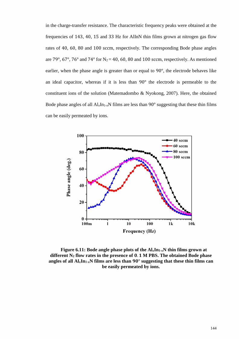
144
in the charge-transfer resistance. The characteristic frequency peaks were obtained at the
frequencies of 143, 40, 15 and 33 Hz for AlInN thin films grown at nitrogen gas flow
rates of 40, 60, 80 and 100 sccm, respectively. The corresponding Bode phase angles
are 79°, 67°, 76° and 74° for N2 = 40, 60, 80 and 100 sccm, respectively. As mentioned
earlier, when the phase angle is greater than or equal to 90°, the electrode behaves like
an ideal capacitor, whereas if it is less than 90° the electrode is permeable to the
constituent ions of the solution (Matemadombo & Nyokong, 2007). Here, the obtained
Bode phase angles of all AlxIn1-xN films are less than 90° suggesting that these thin films
can be easily permeated by ions.
Figure 6.11: Bode angle phase plots of the AlxIn1-xN thin films grown at
different N2 flow rates in the presence of 𝟎. 𝟏 M PBS. The obtained Bode phase
angles of all AlxIn1-xN films are less than 𝟗𝟎° suggesting that these thin films can
be easily permeated by ions.
145
Moreover, the electron recombination lifetime of each sample, 𝜏𝑛, can be measured
from Equation 6.3. The calculated 𝜏𝑛 values of the films deposited at different nitrogen
gas flow rates are shown in Table 6.1 for comparison purposes. It is noteworthy that the
𝜏𝑛 value for the photo-generated charge carriers over the ternary AlxIn1-xN alloy grown at
N2 = 80 sccm is the highest, which could effectively reduce the electron recombination
and thereby enhance photoelectrochemical performance. Hence, the significant decrease
in the Bode phase angle value towards zero and the shift to a lower peak frequency
enhance the permeability of the ions and contribute to the enhancement of the
electrochemical performance.
Electrolyte-based capacitance–voltage measurements were performed to
investigate the variations in electronic properties of the AlxIn1-xN thin films by using
Mott-Schottky (MS) plots, in which 1/(Capacitance)2 is a function of the applied potential
at a frequency of 1 kHz in 0.1 M PBS under dark conditions (Fig. 6.12). The MS plots of
all samples clearly show a positive slope which reflects the n-type properties of the AlxIn1-
xN films.
The donor densities (𝑁𝑑) and flat band potentials (𝑉𝑓𝑏) that were calculated from
Equations (6.1) and (6.2) for the AlxIn1-xN thin films are summarized in Table. 6.1. It can
be seen that there is a shift in 𝑉𝑓𝑏toward negative values from −0.84 to −1.37 V when
the N2 flow rate is increased from 40 to 80 sccm, respectively. Further increase in the N2
flow rate to 100 sccm, shifts the flat band potential back to −1.30 V. It is well-known
that semiconductor materials with a more negative flat band potential have a better ability
to facilitate charge transport in PEC applications (Rai et al., 2014; Yusoff et al., 2015).
This indicates that AlxIn1-xN thin films deposited at nitrogen gas flow rate of 80 sccm has
a significant photoelectrochemical performance which is in good agreement with LSV
results (Figure 6.8). Furthermore, 𝑁𝑑 decreases as the flow rate increase from 40 to
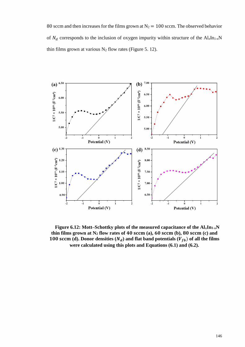
146
80 sccm and then increases for the films grown at N2 = 100 sccm. The observed behavior
of 𝑁𝑑 corresponds to the inclusion of oxygen impurity within structure of the AlxIn1-xN
thin films grown at various N2 flow rates (Figure 5. 12).
Figure 6.12: Mott–Schottky plots of the measured capacitance of the AlxIn1-xN
thin films grown at N2 flow rates of 𝟒𝟎 𝐬𝐜𝐜𝐦 (a), 𝟔𝟎 𝐬𝐜𝐜𝐦 (b), 𝟖𝟎 𝐬𝐜𝐜𝐦 (c) and
𝟏𝟎𝟎 𝐬𝐜𝐜𝐦 (d). Donor densities (𝑵𝒅) and flat band potentials (𝑽𝒇𝒃) of all the films
were calculated using this plots and Equations (6.1) and (6.2).
147
6.4 Summary
The electrochemical properties of InN thin films were investigated in terms of their
water splitting ability in the presence of 0.1 M KOH. Changes in donor density and flat
band potentials with respect to RF power were observed from MS plots. The LSV data
revealed a decrease in the anodic current with increases in nitrogen gas content in the InN
thin films. EIS studies showed that an increase of 𝑅𝑐𝑡 value with RF power leads to
increased resistivity. Bode phase plots suggest that these thin films can be easily
permeable to OH− ions at the InN thin film/electrolyte interface. The good
electrochemical behavior of InN thin films showed that this material could be a potential
candidate for water splitting application. The photoelectrochemical properties of AlxIn1-
xN (0.48 ≤ 𝑥 ≤ 0.66) thin films were investigated for water splitting capability in the
presence of 0.1 M PBS. The PEC results of AlxIn1-xN thin films indicated that the
photocurrent for the AlxIn1-xN thin film grown at N2 flow rate of 80 sccm is ~10-fold
higher than the dark current. EIS results revealed that the 𝑅𝑐𝑡 value of AlxIn1-xN thin film
decreases as the N2 flow rate is increased from 40 to 80 sccm. From the Mott-Schottky
(MS) plots it was deduced that by increasing N2 flow rate up to 80 sccm, the flat band
potential shifts toward more negative values. The good PEC behavior of AlxIn1-xN thin
films grown by plasma-assisted dual source reactive evaporation showed their promising
potential in PEC water splitting application.
148
CHAPTER 7:
CONCLUSION AND SUGGESTIONS FOR FUTURE WORKS
7.1 Overview
This thesis presents the research that was focused on the growth of indium- and
aluminum-based nitride thin films by plasma-assisted reactive evaporation, which to the
best of the author’s knowledge has not been reported by other researchers. The structure,
morphology, optical and electrochemical properties of AlN, InN and AlxIn1-xN thin films
deposited by this technique using a deposition system specifically developed for this work
have been investigated. The most influential growth parameters on specific properties of
each of these films have been investigated in great details to achieve the objectives of this
work as-highlighted in Chapter 1. This work is divided into four important parts in order
to achieve the objectives.
The first part of this work involved the investigations on the structure, composition
and morphology of AlN thin films grown on Si(111) substrate at different filament-
substrate distances. The second part of this work is focused on studying the morphology,
crystallinity, composition and optical properties of InN thin films deposited on Si(111)
and quartz substrates at the different RF powers. The main aim of carrying out these two
parts is to determine the optimized filament-substrate distances and RF power for the
growth of AlxIn1-xN thin films, which is done in the third part of this work. The third part
of this work is divided into three steps. The AC voltages applied to the filament holding
the indium wire were varied in the first step of this part to obtain AlxIn1-xN thin films with
a wide range of elemental compositions covering both In-rich and Al-rich films. The
second step involved studying the effects of nitrogen flow rate on the properties of the
selected Al-rich and In-rich AlxIn1-xN thin films. The last step was performed to study
the stability of the grown AlxIn1-xN alloys at various annealing temperatures. XRD,
149
Raman spectroscopy, FESEM and UV-VIS-NIR spectroscopy techniques were used for
the characterization of the films grown in these three parts of the work. The last part of
this work was conducted to study the electrochemical properties of selected InN and Al-
rich AlxIn1-xN thin films that have been grown in the second and third part of this work.
The aim of this study is to investigate electrochemical (EC) and photoelectrochemical
(PEC) characteristics on the deposited InN and Al-rich AlxIn1-xN thin films, respectively.
The electrochemical behaviors of the InN thin films were investigated in 0.1 M KOH
electrolyte, while for the AlxIn1-xN thin films 0.1 M PBS electrolyte was used. Linear
sweep voltammograms (LSV), electrochemical impedance spectroscopy (EIS), Bode
phase plots, Electrolyte-based capacitance–voltage measurements and cyclic
voltammograms were utilized for electrochemical study of the thin films.
7.2 Conclusion
This work has been successfully carried out and the major findings obtained are
highlighted below:
A simple, cost-effective and environmental-friendly home-built plasma-
assisted reactive evaporation system has been successfully developed for
controlled growth of AlN, InN and AlInN thin films with tunable optical
and electrochemical properties. This deposition system was able to grow
the above-mentioned thin films at high deposition rate.
The filament-to-substrate distance and RF power were shown to have
strong influence on the structure, morphology and composition of AlN and
InN thin films, respectively. The enhancement in surface reaction as a result
of reduced filament-to-substrate distance have led to the growth AlN thin
films with lower presence of metallic phase. Increasing the RF power to a
certain threshold value resulted in highly crystalline InN thin films with
150
higher nitrogen incorporation and lower oxygen contamination due to the
controlled impinging energy of the nitrogen adatoms on the growth sites.
The obtained band gap energy (𝐸𝑔) values of InN thin films grown at
various RF power were fell in the range of 2.0 − 2.5 eV, which is much
higher than reported 𝐸𝑔 values for InN due to unavoidable presence of
oxygen impurity in the film structure.
AlxIn1-xN thin films with different Al (In) mole fractions were obtained by
simply varying the AC voltage that is applied to the filament heating the In
wire. In this work, Al-rich (x=0.64 and 0.60) and In-rich (x=0.18 and 0.10)
AlxIn1-xN thin films were deposited by varying this voltage.
The Raman results established that the A1(LO) phonon mode of the Al-
rich AlxIn1-xN films deposited by plasma-assisted reactive evaporation
exhibit a two-mode behavior. The obtained result confirmed that this is a
characteristic behavior of Al-rich AlxIn1-xN films.
The band gap energy of AlxIn1-xN films deposited by plasma-assisted
reactive evaporation can be tuned within a wide range of energy from
0.9 eV to 2.5 eV by varying specific growth parameters.
The bowing parameter of AlxIn1-xN films that had been deposited in this
work was determined to be 4.3 eV which is close to the values reported in
literature for this type of film grown using various other conventional
techniques.
Nitrogen flow rate was shown to have significant effect on the structure,
morphology and optical properties of In-rich and Al-rich AlxIn1-xN thin
films. Al incorporation (x) into the structure of both In-rich and Al-rich
AlxIn1-xN thin films was decreased with increase in N2 flow rate. Enhanced
151
gas-phase reactions decreased the energy of adatoms reaching on the
growth sites which contributed to the low Al incorporation.
The inclusion of AlN in InN films (In-rich AlxIn1-xN films) that were grown
by reactive evaporation of In and Al wires using dual heated filaments in
N2 plasma ambient resulted in films with band gap energy of 0.9 eV which
is close to the reported band gap energy of InN (0.7 eV);
Annealing studies showed that the optical and structural properties of
AlxIn1-xN films grown by plasma-assisted reactive evaporation are stable at
temperatures below 300 °C for applications in opto-electronic devices.
Unavoidable presence of oxygen impurities in InN thin films was shown to
have favorable effects on the electrochemical properties of the films. It was
shown that the donor density (Nd) of the films grown at different RF power
contain strong dependence on the oxygen content in the thin film. The
nitrogen content in the InN thin films on the other hand, influenced the
anodic current measured by linear sweep voltammogram (LSV).
The photoelectrochemical (PEC) results obtained for AlxIn1-xN thin films
with band gap energy of 2.12 eV showed 10-fold enhancement in the
photocurrent compared to the dark current. The Mott-Schottky (MS) plot
of these films showed that the flat band potential had large negative values
indicating higher ability to facilitate charge transport in PEC applications;
The electrochemical behavior of the InN and AlxIn1-xN thin films grown by
plasma-assisted reactive evaporation technique showed that these films are
promising for EC and PEC water splitting applications, respectively. Both
InN and AlxIn1-xN (0.48 ≤ 𝑥 ≤ 0.66) thin films showed easy permeability
to ions at the film/electrolyte interface during EC process.
152
7.3 Suggestions for Future Work
The results presented here have created a path towards a cost-effective and non-toxic
technique of growing aluminum and indium based nitrides thin films by plasma-assisted
reactive evaporation. However, precise control of the growth parameters, especially
control of the evaporation rate to remove the metallic phase from the films structure is
needed. Investigations on the post-treatment effects on the deposited thin films by using
acidic solutions is strongly recommended for removing the metallic phase from the grown
films. Moreover, for InN and AlN thin films, more precise/detailed analysis techniques
such as XPS and XRF in the bulk form with identical scanning parameters should be
planned for further improve the confidence level of the nitrogen content in the films.
The most serious research problem faced in this work was incorporation of Al atoms
into the AlxIn1-xN structure in a controlled and precise manner due the flash evaporation
behaviour of Al when it reaches melting point. This results in inclusion of Al metal into
the film structure and can be considered as a serious weakness in using this growth
technique. Suggestions for future work is combination of sputtering with the current
growth system where the Al and In atoms are incorporated into the film structure by
sputtering of Al target and evaporation of In wire, respectively.
In situ gas-phase diagnostics techniques such as optical emission spectroscopy (OES),
mass spectroscopy and diode laser absorption (DLA) make it possible to measure the
density of reactive species in the steady state of plasma and may strengthen the existing
model on the growth kinetics of these materials. The concentration of ionic species that
is measured during the various steps of the growth process with respect to the studied
deposition parameters will enable precise control of the parameters for growth of the
studied materials with higher quality.
153
Since the EC and PEC studies of the InN and AlInN thin films done in this work is
only preliminary, further investigations are required to improve the corresponding EC
and PEC behaviors of the grown films. The evaluation of the stability of the grown thin
films is strongly suggested by taking into account the recyclability/reusability of the thin
films during the EC and PEC processes. Effects of the film structure on the EC and PEC
behavior properties are interesting investigations to be pursued for future work.
Investigations in improving the PEC performance with introduction of sacrificial electron
donor such as oxalic acid, methanol and formic acid into the PEC cells can be another
possible future work. Another possible study to be pursued is to introduce some noble
metal dopants on the surface of the AlInN thin films to improve the visible light
absorption and interfacial charge-transfer process which can result in enhancement of the
PEC efficiency.
154
REFERENCES
Abe, R. (2010). Recent progress on photocatalytic and photoelectrochemical water
splitting under visible light irradiation. Journal of Photochemistry and
Photobiology C: Photochemistry Reviews, 11(4), 179-209.
Ager, J. W., Jones, R. E., Yamaguchi, D. M., Yu, K. M., Walukiewicz, W., Li, S. X.,
Haller, E. E., Lu, H., & Schaff, W. J. (2007). p-type InN and In-rich InGaN.
physica status solidi (b), 244(6), 1820-1824.
Ager, J. W., Miller, N., Jones, R. E., Yu, K. M., Wu, J., Schaff, W. J., & Walukiewicz,
W. (2008). Mg-doped InN and InGaN – Photoluminescence, capacitance–voltage
and thermopower measurements. physica status solidi (b), 245(5), 873-877.
Ajagunna, A. O., Adikimenakis, A., Iliopoulos, E., Tsagaraki, K., Androulidaki, M., &
Georgakilas, A. (2009). InN films and nanostructures grown on Si (1 1 1) by RF-
MBE. Journal of Crystal Growth, 311(7), 2058-2062.
Akasaki, I., Amano, H., Sota, S., Sakai, H., Tanaka, T., & Koike, M. (1995). Stimulated
Emission by Current Injection from an AlGaN/GaN/GaInN Quantum Well
Device. Japanese Journal of Applied Physics, 34(11B), L1517-L1519.
Alexandrov, D., Butcher, K. S. A., & Wintrebert-Fouquet, M. (2004). Absorption and
photoluminescence features caused by defects in InN. Journal of Crystal Growth,
269(1), 77-86.
AlOtaibi, B., Nguyen, H., Zhao, S., Kibria, M., Fan, S., & Mi, Z. (2013). Highly stable
photoelectrochemical water splitting and hydrogen generation using a double-
band InGaN/GaN core/shell nanowire photoanode. Nano Letters, 13(9), 4356-
4361.
Amirhoseiny, M., Ng, S. S., & Hassan, Z. (2015). Effect of deposition conditions on
properties of nitrogen rich-InN nanostructures grown on anisotropic Si (110).
Materials Science in Semiconductor Processing, 35, 216-221.
Angerer, H., Brunner, D., Freudenberg, F., Ambacher, O., Stutzmann, M., Höpler, R.,
Metzger, T., Born, E., Dollinger, G., Bergmaier, A., Karsch, S., & Körner, H.-J.
(1997). Determination of the Al mole fraction and the band gap bowing of
epitaxial AlxGa1−xN films. Applied Physics Letters, 71(11), 1504-1506.
Ariffin, S., Lim, H., Talib, Z., Pandikumar, A., & Huang, N. (2015). Aerosol-assisted
chemical vapor deposition of metal oxide thin films for photoelectrochemical
water splitting. International Journal of Hydrogen Energy, 40(5), 2115-2131.
Aryal, K., Pantha, B., Li, J., Lin, J., & Jiang, H. (2010). Hydrogen generation by solar
water splitting using p-InGaN photoelectrochemical cells. Applied Phyics Letter
96, 052110-3.
Avasarala, B., & Haldar, P. (2010). Electrochemical oxidation behavior of titanium
nitride based electrocatalysts under PEM fuel cell conditions. Electrochimica
Acta, 55(28), 9024-9034.
155
Bakalova, S., Szekeres, A., Huhn, G., Havancsak, K., Grigorescu, S., Socol, G., Ristoscu,
C., & Mihailescu, I. N. (2009). Surface morphology of AlN films synthesized by
pulsed laser deposition. Vacuum, 84(1), 155-157.
Barick, B. K., & Dhar, S. (2015). Surface and bulk electronic properties of low
temperature synthesized InN microcrystals. Journal of Crystal Growth, 416, 154-
158.
Bechstedt, F., Furthmüller, J., Ferhat, M., Teles, L. K., Scolfaro, L. M. R., Leite, J. R.,
Davydov, V. Yu, Ambacher, O., & Goldhahn, R. (2003). Energy gap and optical
properties of InxGa1–xN. physica status solidi (a), 195(3), 628-633.
Behrisch, R., & Wittmaack, K. (1983). Sputtering by particle bombardment (Vol. 3):
Springer Berlin.
Berger, C., Dadgar, A., Bläsing, J., & Krost, A. (2013). In-situ growth monitoring of
AlInN/AlGaN distributed Bragg reflectors for the UV-spectral range. Journal of
Crystal Growth, 370, 87-91.
Berreman, D. W. (1963). Infrared Absorption at Longitudinal Optic Frequency in Cubic
Crystal Films. Physical Review, 130(6), 2193-2198.
Bhuiyan, A. G., Hashimoto, A., & Yamamoto, A. (2003). Indium nitride (InN): A review
on growth, characterization, and properties. Journal of Applied Physics, 94(5),
2779-2808.
Biju, K. P., & Jain, M. K. (2008). The effect of rf power on the growth of InN films by
modified activated reactive evaporation. Applied Surface Science, 254(22), 7259-
7265.
Butcher, K., Wintrebert-Fouquet, M., Chen, P.-T., Tansley, T., Dou, H., Shrestha, S.,
Timmers, H., Kuball, M., Prince, K. E., & Bradby, J. (2004). Nitrogen-rich
indium nitride. Journal of Applied Physics, 95(11), 6124-6128.
Butcher, K. S. A., & Tansley, T. L. (2005). InN, latest development and a review of the
band-gap controversy. Superlattices and Microstructures, 38(1), 1-37.
Cai, X.-M., Ye, F., Hao, Y.-Q., Zhang, D.-P., Zhang, Z.-H., & Fan, P. (2009). The
properties of direct current sputtering deposited InN thin films under different gas
flow rates. Journal of Alloys and Compounds, 484(1–2), 677-681.
Chale-Lara, F., Farias, M. H., Huerta-Escamilla, C., & Xiao, M. (2009). Optical
properties of pulse laser deposited AlN thin films on silicon. Materials Letters,
63(24–25), 2093-2096.
Chauhan, A. K. S., Kumar, M., & Gupta, G. (2015). Catalyst free self-assembled growth
of InN nanorings on stepped Si (5 5 3) surface. Applied Surface Science, 345, 156-
161.
Chauhan, D., Dass, S., & Shrivastav, R. Preparation and characterization of
nanostructured CuO thin films for photoelectrochemical splitting of water.
Bulletin of Materials Science, 29 (7) 709-716.
156
Chen, S., & Qiao, S.-Z. (2013). Hierarchically Porous Nitrogen-Doped Graphene–
NiCo2O4 Hybrid Paper as an Advanced Electrocatalytic Water-Splitting Material.
ACS Nano, 7(11), 10190-10196.
Chen, Y., Song, H., Li, D., Sun, X., Jiang, H., Li, Z., Miao, G., Zhang, Z., & Zhou, Y.
(2014). Influence of the growth temperature of AlN nucleation layer on AlN
template grown by high-temperature MOCVD. Materials Letters, 114, 26-28.
Chen, Y., Zhou, X., Zhao, X., He, X., & Gu, X. (2008). Crystallite structure, surface
morphology and optical properties of In2O3–TiO2 composite thin films by sol–gel
method. Materials Science and Engineering: B, 151(2), 179-186.
Chen, Z. T., Tan, S. X., Sakai, Y., & Egawa, T. (2009). Improved performance of InAlN-
based Schottky solar-blind photodiodes. Applied Physics Letters, 94(21), 213504-
3.
Cheng, H., & Hing, P. (2003). The evolution of preferred orientation and morphology of
AlN films under various RF sputtering powers. Surface and Coatings Technology,
167(2–3), 297-301.
Cheng, H., Sun, Y., Zhang, J. X., Zhang, Y. B., Yuan, S., & Hing, P. (2003). AlN films
deposited under various nitrogen concentrations by RF reactive sputtering.
Journal of Crystal Growth, 254(1–2), 46-54.
Cho, A. Y. (1970). Morphology of Epitaxial Growth of GaAs by a Molecular Beam
Method: The Observation of Surface Structures. Journal of Applied Physics,
41(7), 2780-2786.
Cho, S. (2011). Effect of nitrogen flow ratio on the structural and optical properties of
aluminum nitride thin films. Journal of Crystal Growth, 326(1), 179-182.
Chong, S. K., Goh, B. T., Dee, C. F., & Rahman, S. A. (2012). Study on the role of
filament temperature on growth of indium-catalyzed silicon nanowires by the hot-
wire chemical vapor deposition technique. Materials Chemistry and Physics,
135(2–3), 635-643.
Chong, S. K., Goh, B. T., Dee, C. F., & Rahman, S. A. (2013). Effect of substrate to
filament distance on formation and photoluminescence properties of indium
catalyzed silicon nanowires using hot-wire chemical vapor deposition. Thin Solid
Films, 529, 153-158.
Collazo, R., & Dietz III, N. (2013). The group III-nitride material class: From
preparation to perspectives in photoelectrocatalysis: RSC Publishing.
Collazo, R., & Dietz, N. (2013). CHAPTER 8 The Group III-Nitride Material Class: from
Preparation to Perspectives in Photoelectrocatalysis Photoelectrochemical Water
Splitting: Materials, Processes and Architectures (pp. 193-222): The Royal
Society of Chemistry.
Çörekçi, S., Öztürk, M. K., Çakmak, M., Özçelik, S., & Özbay, E. (2012). The influence
of thickness and ammonia flow rate on the properties of AlN layers. Materials
Science in Semiconductor Processing, 15(1), 32-36.
157
Costales, A., Blanco, M. A., Martín Pendás, Á., Kandalam, A. K., & Pandey, R. (2002).
Chemical Bonding in Group III Nitrides. Journal of the American Chemical
Society, 124(15), 4116-4123.
Cowan, A. J., & Durrant, J. R. (2013). Long-lived charge separated states in
nanostructured semiconductor photoelectrodes for the production of solar fuels.
Chemical Society Reviews, 42(6), 2281-2293.
Darakchieva, V., Xie, M.-Y., Tasnádi, F., Abrikosov, I. A., Hultman, L., Monemar, B.,
Kamimura, J., & Kishino, K. (2008). Lattice parameters, deviations from
Vegard’s rule, and E2 phonons in InAlN. Applied Physics Letters, 93(26),
261908-3.
Daudin, B., Rouvière, J. L., & Arlery, M. (1996). Polarity determination of GaN films by
ion channeling and convergent beam electron diffraction. Applied Physics Letters,
69(17), 2480-2482.
Davydov, V. Y., Klochikhin, A., Seisyan, R., Emtsev, V., Ivanov, S., Bechstedt, F.,
Furthmüller, J., Harima, H., Mudryi, A. V., & Aderhold, J. (2002). Absorption
and emission of hexagonal InN. Evidence of narrow fundamental band gap.
physica status solidi (b), 229(3), r1-r3.
Davydov, V. Y., Klochikhin, A. A., Seisyan, R. P., Emtsev, V. V., Ivanov, S. V.,
Bechstedt, F., Furthmüller, J., Harima, H., Mudryi, A. V., Aderhold, J.,
Semchinova, O., & Graul, J. (2002). Absorption and Emission of Hexagonal InN.
Evidence of Narrow Fundamental Band Gap. physica status solidi (b), 229(3), r1-
r3.
Demangeot, F., Groenen, J., Frandon, J., Renucci, M. A., Briot, O., Clur, S., &
Aulombard, R. L. (1998). Coupling of GaN- and AlN-like longitudinal optic
phonons in Ga1−xAlxN solid solutions. Applied Physics Letters, 72(21), 2674-
2676.
Deutsch, T. G., Koval, C. A., & Turner, J. A. (2006). III−V Nitride Epilayers for
Photoelectrochemical Water Splitting: GaPN and GaAsPN. The Journal of
Physical Chemistry B, 110(50), 25297-25307.
Dixit, A., Sudakar, C., Thakur, J. S., Padmanabhan, K., Kumar, S., Naik, R., Naik, V. M.,
& Lawes, G. (2009). Strong plasmon absorption in InN thin films. Journal of
Applied Physics, 105(5), 053104-5.
Ferhat, M., & Bechstedt, F. (2002). First-principles calculations of gap bowing in
Inx Ga1−xN and InxAl1−xN alloys: Relation to structural and thermodynamic
properties. Physical Review B, 65(7), 075213-7.
Fernández-Garrido, S., Gačević, Ž., & Calleja, E. (2008). A comprehensive diagram to
grow InAlN alloys by plasma-assisted molecular beam epitaxy. Applied Physics
Letters, 93(19), 191907-3.
Fichter, F. (1907). Über Aluminiumnitrid. Zeitschrift für anorganische Chemie, 54(1),
322-327.
158
Flynn, C., & Sim, L. W. (2015). Effects of phosphoric acid on the surface morphology
and reflectance of AlN grown by MBE under Al-rich conditions. Thin Solid Films,
589, 338-343.
Fujishima, A., & Honda, K. (1972). Electrochemical Photolysis of Water at a
Semiconductor Electrode. Nature, 238(5358), 37-38.
García-Gancedo, L., Zhu, Z., Iborra, E., Clement, M., Olivares, J., Flewitt, A. J., Milne,
W. I., Ashley, G. M., Luo, J. K., Zhao, X. B., & Lu, J. R. (2011). AlN-based BAW
resonators with CNT electrodes for gravimetric biosensing. Sensors and Actuators
B: Chemical, 160(1), 1386-1393.
Goh, B. T. (2012). Layer-by-layer plasma enhanced chemical vapour deposition of
nanocrystalline silicon thin films/Goh Boon Tong. University of Malaya.
Goldhahn, R., Schley, P., Winzer, A. T., Gobsch, G., Cimalla, V., Ambacher, O., Rakel,
M., Cobet, C., Esser, N., Lu, H., & Schaff, W. J. (2006). Detailed analysis of the
dielectric function for wurtzite InN and In-rich InAlN alloys. physica status solidi
(a), 203(1), 42-49.
Guo, J., & Chen, X. (2011). Solar hydrogen generation: transition metal oxides in water
photoelectrolysis: McGraw Hill Professional.
Guo, L., Yang, J., Feng, Y., Qiu, T., Chen, B., & Wan, W. (2016). Preparation and
properties of AlN ceramic suspension for non-aqueous gel casting. Ceramics
International, 42(7), 8066-8071.
Guo, L. a., Chen, G., Zhu, Y., Duan, X., & Ye, H. (2015). The growth of Sea-urchin-like
AlN nanostructures by modified CVD and their Field Emission properties.
Journal of Crystal Growth, 426, 49-53.
Guo, Q., Nakao, T., Ushijima, T., Shi, W., Liu, F., Saito, K., Tanaka, T., & Nishio, M.
(2014). Growth of InGaN layers on (1 1 1) silicon substrates by reactive
sputtering. Journal of Alloys and Compounds, 587, 217-221.
Guo, Q., Okada, A., Kidera, H., Nishio, M., & Ogawa, H. (2000). Growth of AlInN on
(111)GaAs Substrates. Japanese Journal of Applied Physics, 39(11B), L1143-
L1145.
Guo, Q., Tanaka, T., Nishio, M., & Ogawa, H. (2003). Optical Bandgap Energy of
Wurtzite In-Rich AlInN Alloys. Japanese Journal of Applied Physics, 42(2B),
L141-L143.
Guo, Q., Tanaka, T., Nishio, M., & Ogawa, H. (2008). Structural and Optical Properties
of AlInN Films Grown on Sapphire Substrates. Japanese Journal of Applied
Physics, 47(1S), 612-615.
Guo, Q. X., Okazaki, Y., Kume, Y., Tanaka, T., Nishio, M., & Ogawa, H. (2007).
Reactive sputter deposition of AlInN thin films. Journal of Crystal Growth,
300(1), 151-154.
159
Guo, Q. X., Tanaka, T., Nishio, M., & Ogawa, H. (2006). Growth properties of AlN films
on sapphire substrates by reactive sputtering. Vacuum, 80(7), 716-718.
He, H., Cao, Y., Fu, R., Guo, W., Huang, Z., Wang, M., Huang, C., Huang, J., & Wang,
H. (2010). Band gap energy and bowing parameter of In-rich InAlN films grown
by magnetron sputtering. Applied Surface Science, 256(6), 1812-1816.
Hobert, H., Dunken, H. H., Meinschien, J., & Stafast, H. (1999). Infrared and Raman
spectroscopic investigation of thin films of AlN and SiC on Si substrates.
Vibrational Spectroscopy, 19(2), 205-211.
Hoi Wong, M., Wu, F., Hurni, C. A., Choi, S., Speck, J. S., & Mishra, U. K. (2012).
Molecular beam epitaxy of InAlN lattice-matched to GaN with homogeneous
composition using ammonia as nitrogen source. Applied Physics Letters, 100(7),
072107-3.
Höök, M., & Tang, X. (2013). Depletion of fossil fuels and anthropogenic climate
change—A review. Energy Policy, 52, 797-809.
Hovel, H. J., & Cuomo, J. J. (1972). Electrical and Optical Properties of rf‐Sputtered GaN
and InN. Applied Physics Letters, 20(2), 71-73.
Hwang, Y. J., Wu, C. H., Hahn, C., Jeong, H. E., & Yang, P. (2012). Si/InGaN Core/Shell
Hierarchical Nanowire Arrays and their Photoelectrochemical Properties. Nano
Letters, 12(3), 1678-1682.
Inushima, T., Shiraishi, T., & Davydov, V. Y. (1999). Phonon structure of InN grown by
atomic layer epitaxy. Solid State Communications, 110(9), 491-495.
Ivanov, S. V., Shubina, T. V., Komissarova, T. A., & Jmerik, V. N. (2014). Metastable
nature of InN and In-rich InGaN alloys. Journal of Crystal Growth, 403, 83-89.
Jagannadham, K., Sharma, A. K., Wei, Q., Kalyanraman, R., & Narayan, J. (1998).
Structural characteristics of AlN films deposited by pulsed laser deposition and
reactive magnetron sputtering: A comparative study. Journal of Vacuum Science
& Technology A, 16(5), 2804-2815.
Jejurikar, S. M., Banpurkar, A. G., Bankar, D. N., Adhi, K. P., Kukreja, L. M., & Sathe,
V. G. (2007). Growth temperature and N2 ambient pressure-dependent crystalline
orientations and band gaps of pulsed laser-deposited AlN/(0 0 0 1) sapphire thin
films. Journal of Crystal Growth, 304(1), 257-263.
Jeong, M. W., Jeon, S. W., Lee, S. H., & Kim, Y. (2015). Effective heat dissipation and
geometric optimization in an LED module with aluminum nitride (AlN) insulation
plate. Applied Thermal Engineering, 76, 212-219.
Ji, X. H., Lau, S. P., Yang, H. Y., & Zhang, Q. Y. (2007). Structural and optical properties
of wurtzite InN grown on Si(111). Thin Solid Films, 515(11), 4619-4623.
Jiang, L. F., Kong, J. F., Shen, W. Z., & Guo, Q. X. (2011). Temperature dependence of
Raman scattering in AlInN. Journal of Applied Physics, 109(11), 113514-5.
160
Johnson, W. C., & Parsons, J. B. (1931). Nitrogen Compounds of Gallium. I, II. The
Journal of Physical Chemistry, 36(10), 2588-2594.
Jothibas, M., Manoharan, C., Ramalingam, S., Dhanapandian, S., Johnson Jeyakumar, S.,
& Bououdina, M. (2013). Preparation, characterization, spectroscopic (FT-IR,
FT-Raman, UV and visible) studies, optical properties and Kubo gap analysis of
In2O3 thin films. Journal of Molecular Structure, 1049(0), 239-249.
Juodkazytė, J., Šebeka, B., Savickaja, I., Kadys, A., Jelmakas, E., Grinys, T., Juodkazis,
S., Juodkazis, K., Malinauskas, T. (2014). InxGa1−xN performance as a band-gap-
tunable photo-electrode in acidic and basic solutions. Solar Energy Materials and
Solar Cells, 130, 36-41.
Kallel, T., Dammak, M., Wang, J., & Jadwisienczak, W. M. (2014). Raman
characterization and stress analysis of AlN:Er3+ epilayers grown on sapphire and
silicon substrates. Materials Science and Engineering: B, 187, 46-52.
Kamimura, J., Kouno, T., Ishizawa, S., Kikuchi, A., & Kishino, K. (2007). Growth of
high-In-content InAlN nanocolumns on Si (1 1 1) by RF-plasma-assisted
molecular-beam epitaxy. Journal of Crystal Growth, 300(1), 160-163.
Kang, T.-T., Hashimoto, A., & Yamamoto, A. (2009). Raman scattering of indium-rich
AlxIn1-xN : Unexpected two-mode behavior of A1(LO) . Physical Review B, 79(3),
033301-4.
Kang, T.-T., Yamamoto, M., Tanaka, M., Hashimoto, A., & Yamamoto, A. (2009). Effect
of gas flow on the growth of In-rich AlInN films by metal-organic chemical vapor
deposition. Journal of Applied Physics, 106(5), 053525-4.
Kelekci, O., Tasli, P., Cetin, S. S., Kasap, M., Ozcelik, S., & Ozbay, E. (2012).
Investigation of AlInN HEMT structures with different AlGaN buffer layers
grown on sapphire substrates by MOCVD. Current Applied Physics, 12(6), 1600-
1605.
Khan, S., Mehmood, M., Saeed, S., Khan, T. M., Sadiq, G., & Ahmed, I. (2013). Effect
of substrate biasing and temperature on AlN thin film deposited by cathodic arc
ion. Materials Science in Semiconductor Processing, 16(3), 640-646.
Kibria, M. G., Nguyen, H. P., Cui, K., Zhao, S., Liu, D., Guo, H., Trudeau, M. L., Paradis,
S., Hakima, A. R., & Mi, Z. (2013). One-step overall water splitting under visible
light using multiband InGaN/GaN nanowire heterostructures. ACS Nano, 7(9),
7886-7893.
King, P. D. C., Veal, T. D., Jefferson, P. H., McConville, C. F., Wang, T., Parbrook, P.
J., Lu, H., & Schaff, W. J. (2007). Valence band offset of InN∕AlN heterojunctions
measured by x-ray photoelectron spectroscopy. Applied Physics Letters, 90(13),
132105-3.
Kocha, S. S., & Turner, J. A. (1995). Displacement of the Bandedges of GaInP2 in
Aqueous Electrolytes Induced by Surface Modification. Journal of The
Electrochemical Society, 142(8), 2625-2630.
161
Kuang, X.-P., Zhang, H.-Y., Wang, G.-G., Cui, L., Zhu, C., Jin, L., Sun, R., & Han, J.-C.
(2012a). AlN films prepared on 6H–SiC substrates under various sputtering
pressures by RF reactive magnetron sputtering. Applied Surface Science, 263, 62-
68.
Kuang, X.-P., Zhang, H.-Y., Wang, G.-G., Cui, L., Zhu, C., Jin, L., Sun, R., & Han, J.-C.
(2012b). AlN films prepared on 6H–SiC substrates under various sputtering
pressures by RF reactive magnetron sputtering. Applied Surface Science, 263(0),
62-68.
Kuang, X.-P., Zhang, H.-Y., Wang, G.-G., Cui, L., Zhu, C., Jin, L., Sun, R., & Han, J.-C.
(2012c). Effect of deposition temperature on the microstructure and surface
morphology of c-axis oriented AlN films deposited on sapphire substrate by RF
reactive magnetron sputtering. Superlattices and Microstructures, 52(5), 931-940.
Kubota, K., Kobayashi, Y., & Fujimoto, K. (1989). Preparation and properties of III‐V
nitride thin films. Journal of Applied Physics, 66(7), 2984-2988.
Kucera, M., Wistrela, E., Pfusterschmied, G., Ruiz-Díez, V., Manzaneque, T., Hernando-
García, J., Sánchez-Rojas, J. L., Jachimowicz, A., Schalko, J., Bittner, A., &
Schmid, U. (2014). Design-dependent performance of self-actuated and self-
sensing piezoelectric-AlN cantilevers in liquid media oscillating in the
fundamental in-plane bending mode. Sensors and Actuators B: Chemical, 200,
235-244.
Kudo, A., & Miseki, Y. (2009). Heterogeneous photocatalyst materials for water splitting.
Chemical Society Reviews, 38(1), 253-278.
Kumar, M., Bhat, T. N., Rajpalke, M. K., Roul, B., Kalghatgi, A. T., & Krupanidhi, S. B.
(2012). Indium flux, growth temperature and RF power induced effects in InN
layers grown on GaN/Si substrate by plasma-assisted MBE. Journal of Alloys and
Compounds, 513, 6-9.
Kumar, M., Rajpalke, M. K., Bhat, T. N., Roul, B., Sinha, N., Kalghatgi, A. T., &
Krupanidhi, S. B. (2011). Growth of InN layers on Si (111) using ultra thin silicon
nitride buffer layer by NPA-MBE. Materials Letters, 65(9), 1396-1399.
Kumar, S., Li Mo, Motlan, & Tansley, Trevor L. (1996). Elemental Composition of
Reactively Sputtered Indium Nitride Thin Films. Japanese Journal of Applied
Physics, 35(4R), 2261-2265.
Lebedev, V., Morales, F. M., Cimalla, V., Lozano, J. G., González, D., Himmerlich, M.,
Krischok, S., Schaefer, J. A., & Ambacher, O. (2006). Correlation between
structural and electrical properties of InN thin films prepared by molecular beam
epitaxy. Superlattices and Microstructures, 40(4–6), 289-294.
Lee, M.-C., Lin, H.-C., Pan, Y.-C., Shu, C.-K., Ou, J., Chen, W.-H., & Chen, W.-K.
(1998). Raman and x-ray studies of InN films grown by metalorganic vapor phase
epitaxy. Applied Physics Letters, 73(18), 2606-2608.
162
Li, G., Wang, W., Yang, W., & Wang, H. (2015). Epitaxial growth of group III-nitride
films by pulsed laser deposition and their use in the development of LED devices.
Surface Science Reports, 70(3), 380-423.
Li, J., Lin, J., & Jiang, H. (2008). Direct hydrogen gas generation by using InGaN
epilayers as working electrodes. Applied Physics Letters, 93(16), 162107-3.
Li, X., Kong, L., Shen, L., Yang, J., Gao, M., Hu, T., Wu, X., & Li, M. (2013). Synthesis
and in situ high pressure Raman spectroscopy study of AlN dendritic crystal.
Materials Research Bulletin, 48(9), 3310-3314.
Liu, B., Gao, J., Wu, K. M., & Liu, C. (2009). Preparation and rapid thermal annealing of
AlN thin films grown by molecular beam epitaxy. Solid State Communications,
149(17–18), 715-717.
Liu, H. F., Li, C. G., Ansah Antwi, K. K., Chua, S. J., & Chi, D. Z. (2014). Electron-
beam-induced carbon deposition on high-indium-content AlInN thin films grown
on Si by sputtering at elevated temperature. Materials Letters, 128(0), 344-348.
Liu, H. F., Tan, C. C., Dalapati, G. K., & Chi, D. Z. (2012). Magnetron-sputter deposition
of high-indium-content n-AlInN thin film on p-Si(001) substrate for photovoltaic
applications. Journal of Applied Physics, 112(6), 063114-5.
Liu, S.-Y., Sheu, J. K., Lin, Y.-C., Chen, Y.-T., Tu, S. J., Lee, M. L., & Lai, W. C. (2013).
InGaN working electrodes with assisted bias generated from GaAs solar cells for
efficient water splitting. Optics Express, 21(S6), A991-A996.
Loudon, R. (1964). The Raman effect in crystals. Advances in Physics, 13(52), 423-482.
Lukitsch, M. J., Danylyuk, Y. V., Naik, V. M., Huang, C., Auner, G. W., Rimai, L., &
Naik, R. (2001). Optical and electrical properties of Al1−xInxN films grown by
plasma source molecular-beam epitaxy. Applied Physics Letters, 79(5), 632-634.
Maeda, K. (2011). Photocatalytic water splitting using semiconductor particles: history
and recent developments. Journal of Photochemistry and Photobiology C:
Photochemistry Reviews, 12(4), 237-268.
Maeda, K., & Domen, K. (2007). New non-oxide photocatalysts designed for overall
water splitting under visible light. The Journal of Physical Chemistry C, 111(22),
7851-7861.
Maeda, K., & Domen, K. (2011). Oxynitride materials for solar water splitting. MRS
bulletin, 36(01), 25-31.
Manasevit, H. M., Erdmann, F. M., & Simpson, W. I. (1971). The Use of Metalorganics
in the Preparation of Semiconductor Materials: IV . The Nitrides of Aluminum
and Gallium. Journal of The Electrochemical Society, 118(11), 1864-1868.
Manivasakan, P., Ramasamy, P., & Kim, J. (2014). Use of urchin-like Nix Co3− xO4
hierarchical nanostructures based on non-precious metals as bifunctional
electrocatalysts for anion-exchange membrane alkaline alcohol fuel cells.
Nanoscale, 6(16), 9665-9672.
163
Mansurov, V. G., Nikitin, A. Y., Galitsyn, Y. G., Svitasheva, S. N., Zhuravlev, K. S.,
Osvath, Z., Dobos, L., Horvath, Z. E., & Pecz, B. (2007). AlN growth on sapphire
substrate by ammonia MBE. Journal of Crystal Growth, 300(1), 145-150.
Martin, G., Botchkarev, A., Rockett, A., & Morkoç, H. (1996). Valence‐band
discontinuities of wurtzite GaN, AlN, and InN heterojunctions measured by x‐ray
photoemission spectroscopy. Applied Physics Letters, 68(18), 2541-2543.
Maruska, H. P., & Tietjen, J. J. (1969). THE PREPARATION AND PROPERTIES OF
VAPOR‐DEPOSITED SINGLE‐CRYSTAL‐LINE GaN. Applied Physics
Letters, 15(10), 327-329.
Matemadombo, F., & Nyokong, T. (2007). Characterization of self-assembled
monolayers of iron and cobalt octaalkylthiosubstituted phthalocyanines and their
use in nitrite electrocatalytic oxidation. Electrochimica Acta, 52(24), 6856-6864.
Matsuoka, T. (1997). Calculation of unstable mixing region in wurtzite In1−x−yGaxAlyN.
Applied Physics Letters, 71(1), 105-106.
Matsuoka, T., Okamoto, H., Nakao, M., Harima, H., & Kurimoto, E. (2002). Optical
bandgap energy of wurtzite InN. Applied Physics Letters, 81(7), 1246-1248.
Matsuoka, T., Okamoto, H., Takahata, H., Mitate, T., Mizuno, S., Uchiyama, Y., &
Makimoto, T. (2004). MOVPE growth and photoluminescence of wurtzite InN.
Journal of Crystal Growth, 269(1), 139-144.
Medjdoub, F., Carlin, J. F., Gonschorek, M., Feltin, E., Py, M. A., Ducatteau, D.,
Gaquiere, C., Grandjean, N., & Kohn, E. (2006, 11-13 Dec. 2006). Can
InAlN/GaN be an alternative to high power / high temperature AlGaN/GaN
devices? Paper presented at the Electron Devices Meeting, 2006. IEDM '06.
International, page 1-4, IEEE.
Miao, H., Ji, R., Hu, X., Han, L., Hao, Y., Sun, Q., Zhang, D., Fan, J., Bai, J., & Hou, X.
(2015). Y2O3: Eu3+, Tb3+ spherical particles based anti-reflection and wavelength
conversion bi-functional films: Synthesis and application to solar cells. Journal of
Alloys and Compounds, 629, 74-79.
Mitamura, K., Honke, T., Ohta, J., Kobayashi, A., Fujioka, H., & Oshima, M. (2009).
Characteristics of InN grown directly on Al2O3 (0 0 0 1) substrates by pulsed
laser deposition. Journal of Crystal Growth, 311(5), 1316-1320.
Mohd Yusoff, M. Z., Mahyuddin, A., Hassan, Z., Yusof, Y., Ahmad, M. A., Chin, C. W.,
Hassan, H. A., & Abdullah, M. J. (2013). Plasma-assisted MBE growth of
AlN/GaN/AlN heterostructures on Si (1 1 1) substrate. Superlattices and
Microstructures, 60, 500-507.
Monemar, B., Paskov, P. P., & Kasic, A. (2005). Optical properties of InN—the bandgap
question. Superlattices and Microstructures, 38(1), 38-56.
Nardelli, M. B., Rapcewicz, K., & Bernholc, J. (1997). Strain effects on the interface
properties of nitride semiconductors. Physical Review B, 55(12), R7323-R7326.
164
Naveed ul Hassan, A., Paul, E. D. S. R., Victor, J. G., Praveen, K., Magnus, W., &
Richard, N. (2013). Highly Sensitive and Fast Anion-Selective InN Quantum Dot
Electrochemical Sensors. Applied Physics Express, 6(11), 115201-4.
Ng, S. S., Ooi, P. K., Lee, S. C., Hassan, Z., & Abu Hassan, H. (2012). Surface phonon
polariton of wurtzite AlN thin film grown on sapphire. Materials Chemistry and
Physics, 134(1), 493-498.
Ni, M., Leung, M. K., Leung, D. Y., & Sumathy, K. (2007). A review and recent
developments in photocatalytic water-splitting using TiO2 for hydrogen
production. Renewable and Sustainable Energy Reviews, 11(3), 401-425.
Ohba, R., Mitamura, K., Shimomoto, K., Fujii, T., Kawano, S., Ohta, J., Fujioka, & H.,
Oshima, M. (2009). Growth of cubic InN films with high phase purity by pulsed
laser deposition. Journal of Crystal Growth, 311(11), 3130-3132.
Ooi, P. K., Lee, S. C., Ng, S. S., Hassan, Z., Abu Hassan, H., & Chen, W. L. (2011).
Polarized infrared reflectance studies for wurtzite InN epilayers on Si(111) grown
by molecular beam expitaxy. Thin Solid Films, 520(2), 739-742.
Ostrikov, K. (2005). Colloquium: Reactive plasmas as a versatile nanofabrication tool.
Reviews of Modern Physics, 77(2), 489-511.
Othman, M. (2012). Plasma enhanced chemical vapour deposition of carbon nitride films
from ethane and nitrogen gas mixtures/Maisara binti Othman. University Malaya.
Ozgit, C., Donmez, I., Alevli, M., & Biyikli, N. (2012). Self-limiting low-temperature
growth of crystalline AlN thin films by plasma-enhanced atomic layer deposition.
Thin Solid Films, 520(7), 2750-2755.
Pearton, S. J., Zolper, J. C., Shul, R. J., & Ren, F. (1999). GaN: Processing, defects, and
devices. Journal of Applied Physics, 86(1), 1-78.
Peng, T., Piprek, J., Qiu, G., Olowolafe, J. O., Unruh, K. M., Swann, C. P., & Schubert,
E. F. (1997). Band gap bowing and refractive index spectra of polycrystalline
AlxIn1−xN films deposited by sputtering. Applied Physics Letters, 71(17), 2439-
2441.
Persson, C., Sernelius, B. E., Ferreira da Silva, A., Araújo, C. M., Ahuja, R., & Johansson,
B. (2002). Optical and reduced band gap in n- and p-type GaN and AlN. Journal
of Applied Physics, 92(6), 3207-3216.
Rai, S., Ikram, A., Sahai, S., Dass, S., Shrivastav, R., & Satsangi, V. R. (2014).
Morphological, optical and photoelectrochemical properties of Fe2O3–GNP
composite thin films. RSC Advances, 4(34), 17671-17679.
Reboredo, F. A., Pizzagalli, L., & Galli, G. (2004). Computational Engineering of the
Stability and Optical Gaps of SiC Quantum Dots. Nano Letters, 4(5), 801-804.
Ristoscu, C., Ducu, C., Socol, G., Craciunoiu, F., & Mihailescu, I. N. (2005). Structural
and optical characterization of AlN films grown by pulsed laser deposition.
Applied Surface Science, 248(1–4), 411-415.
165
Rodríguez-Madrid, J. G., Iriarte, G. F., Araujo, D., Villar, M. P., Williams, O. A., Müller-
Sebert, W., & Calle, F. (2012). Optimization of AlN thin layers on diamond
substrates for high frequency SAW resonators. Materials Letters, 66(1), 339-342.
Romero, M. F., Feneberg, M., Moser, P., Berger, C., Bläsing, J., Dadgar, A., Krost, A.,
Sakalauskas, E., & Goldhahn, R. (2012). Luminescence from two-dimensional
electron gases in InAlN/GaN heterostructures with different In content. Applied
Physics Letters, 100(21), 212101-3.
Rosenberger, L., Baird, R., McCullen, E., Auner, G., & Shreve, G. (2008). XPS analysis
of aluminum nitride films deposited by plasma source molecular beam epitaxy.
Surface and Interface Analysis, 40(9), 1254-1261.
Saidi, I., Mejri, H., Baira, M., & Maaref, H. (2015). Electronic and transport properties
of AlInN/AlN/GaN high electron mobility transistors. Superlattices and
Microstructures, 84, 113-125.
Sakai, Y., Khai, P. C., Ichikawa, J., Egawa, T., & Jimbo, T. (2011). Characterization of
AlInN/GaN structures on AlN templates for high-performance ultraviolet
photodiodes. Journal of Applied Physics, 109(3), 033512-6.
Sánchez, G., Tristant, P., Dublanche-Tixier, C., Tétard, F., & Bologna Alles, A. (2014).
Effect of low RF bias potential on AlN films obtained by Microwave Plasma
Enhanced Chemical Vapor Deposition. Surface and Coatings Technology, 256, 3-
8.
Sánchez, G., Wu, A., Tristant, P., Tixier, C., Soulestin, B., Desmaison, J., & Bologna
Alles, A. (2008). Polycrystalline AlN films with preferential orientation by
plasma enhanced chemical vapor deposition. Thin Solid Films, 516(15), 4868-
4875.
Sasaoka, T., Mori, M., Miyazaki, T., & Adachi, S. (2010). Room-temperature infrared
photoluminescence from sputter-deposited InN films. Journal of Applied Physics,
108(6), 063538-5.
Schmidt, T. J., Yang, X. H., Shan, W., Song, J. J., Salvador, A., Kim, W., Aktas, Ö.,
Botchkarev, A., & Morkoç, H. (1996). Room‐temperature stimulated emission in
GaN/AlGaN separate confinement heterostructures grown by molecular beam
epitaxy. Applied Physics Letters, 68(13), 1820-1822.
Shah, A., & Mahmood, A. (2012). Effect of Cr implantation on structural and optical
properties of AlN thin films. Physica B: Condensed Matter, 407(19), 3987-3991.
Shih, C.-H., Lo, I., Pang, W.-Y., & Hiseh, C.-H. (2010). Growth of InN thin films on ZnO
substrate by plasma-assisted molecular beam epitaxy. Journal of Physics and
Chemistry of Solids, 71(12), 1664-1668.
Shinar, R., & Kennedy, J. H. (1982). Photoactivity of doped α-Fe2O3 electrodes. Solar
Energy Materials, 6(3), 323-335.
166
Shinoda, H., & Mutsukura, N. (2002). Deposition of an InN thin film by a r.f. plasma-
assisted reactive ion-beam sputtering deposition (R-IBSD) technique. Diamond
and Related Materials, 11(3–6), 896-900.
Shubina, T., Ivanov, S., Jmerik, V., Solnyshkov, D., Vekshin, V., Kop’ev, P., Vasson, A.,
Leymarie, J., Kavokin, A., & Amano, H. (2005). Erratum: Mie Resonances,
Infrared Emission, and the Band Gap of InN [Phys. Rev. Lett. 92, 117407 (2004)].
Physical Review Letters, 95(20), 209901-1.
Shubina, T. V., Ivanov, S. V., Jmerik, V. N., Solnyshkov, D. D., Vekshin, V. A., Kop’ev,
P. S., Vasson, A., Leymarie, J., Kavokin, A., Amano, H., Shimono, K., Kasic, A.,
& Monemar, B. (2004). Mie Resonances, Infrared Emission, and the Band Gap of
InN. Physical Review Letters, 92(11), 117407-4.
Shukla, G., & Khare, A. (2008). Dependence of N2 pressure on the crystal structure and
surface quality of AlN thin films deposited via pulsed laser deposition technique
at room temperature. Applied Surface Science, 255(5, Part 1), 2057-2062.
Siegle, H., Kaczmarczyk, G., Filippidis, L., Litvinchuk, A. P., Hoffmann, A., & Thomsen,
C. (1997). Zone-boundary phonons in hexagonal and cubic GaN. Physical Review
B, 55(11), 7000-7004.
Singh, A. V., Chandra, S., & Bose, G. (2011). Deposition and characterization of c-axis
oriented aluminum nitride films by radio frequency magnetron sputtering without
external substrate heating. Thin Solid Films, 519(18), 5846-5853.
Skuridina, D., Dinh, D. V., Pristovsek, M., Lacroix, B., Chauvat, M. P., Ruterana, P.,
Kneissl, M., & Vogt, P. (2014). Surface and crystal structure of nitridated sapphire
substrates and their effect on polar InN layers. Applied Surface Science, 307, 461-
467.
Sofikiti, N., Chaniotakis, N., Grandal, J., Utrera, M., Sánchez-García, M. A., & Calleja,
E. (2010). GaN and InN nanocolumns as electrochemical sensing elements:
Potentiometric response to KCl, pH and urea. Materials Letters, 64(12), 1332-
1335.
Soh, J.-W., Jang, S.-S., Jeong, I.-S., & Lee, W.-J. (1996). C-axis orientation of AlN films
prepared by ECR PECVD. Thin Solid Films, 279(1–2), 17-22.
Stokker-Cheregi, F., Nedelcea, A., Filipescu, M., Moldovan, A., Colceag, D., Ion, V.,
Bîrjega, R., & Dinescu, M. (2011). High temperature growth of InN on various
substrates by plasma-assisted pulsed laser deposition. Applied Surface Science,
257(12), 5312-5314.
Sumitani, K., Ohtani, R., Yoshida, T., Nakagawa, Y., Mohri, S., & Yoshitake, T. (2010).
Influences of repetition rate of laser pulses on growth of crystalline AlN films on
sapphire(0001) substrates by pulsed laser deposition. Diamond and Related
Materials, 19(5–6), 618-620.
Sundaresan, B., Vasumathi, A., Ravichandran, K., Ravikumar, P., & Sakthivel, B. (2012).
Annealing effect on physical properties of spin coated ZnO films. Surface
Engineering, 28(5), 323-328.
167
Suzuki, T., Hibino, S., Katayama, R., Kato, Y., Ohashi, F., Itoh, T., & Nonomura, S.
(2013). Effects of Substrate Temperature on Properties of Amorphous InxGa1- xN
Films Deposited by Reactive Radio Frequency Sputtering. Japanese Journal of
Applied Physics, 52(11S), 11NG05-4.
Tachibana, Y., Vayssieres, L., & Durrant, J. R. (2012). Artificial photosynthesis for solar
water-splitting. Nature Photonics, 6(8), 511-518.
Tauc, J. (1974). Amorphous and liquid semiconductors, edited by J. Tauc. London, New
York: Plenum.
Terashima, W., Che, S.-B., Ishitani, Y., & Yoshikawa, A. (2006). Growth and
Characterization of AlInN Ternary Alloys in Whole Composition Range and
Fabrication of InN/AlInN Multiple Quantum Wells by RF Molecular Beam
Epitaxy. Japanese Journal of Applied Physics, 45(6L), L539-L542.
Terziyska, P. T., Butcher, K. S. A., Rafailov, P., & Alexandrov, D. (2015). Growth of
vertically oriented InN nanorods from In-rich conditions on unintentionally
patterned sapphire substrates. Applied Surface Science, 353, 103-105.
Tran, A. T., Wunnicke, O., Pandraud, G., Nguyen, M. D., Schellevis, H., & Sarro, P. M.
(2013). Slender piezoelectric cantilevers of high quality AlN layers sputtered on
Ti thin film for MEMS actuators. Sensors and Actuators A: Physical, 202, 118-
123.
Ueno, M., Yoshida, M., Onodera, A., Shimomura, O., & Takemura, K. (1994). Stability
of the wurtzite-type structure under high pressure: GaN and InN. Physical Review
B, 49(1), 14-21.
Valdueza-Felip, S., Ibáñez, J., Monroy, E., González-Herráez, M., Artús, L., & Naranjo,
F. B. (2012). Improvement of InN layers deposited on Si(111) by RF sputtering
using a low-growth-rate InN buffer layer. Thin Solid Films, 520(7), 2805-2809.
Vernon, C., Thompson, E., & Cornell, S. (2011). Carbon dioxide emission scenarios:
limitations of the fossil fuel resource. Procedia Environmental Sciences, 6, 206-
215.
Vickerman, J. (1997). Surface Analysis: Techniques and Applications: Wiley.
Vijayalakshmi, K., & Pillay, V. V. (2014). Influence of deposition time on the
microstructure and dielectric properties of AlN/Si thin films for enhanced
hydrogen sensing application. Microelectronic Engineering, 113, 29-34.
Voznyy, A. V., & Deibuk, V. G. (2004). The role of alloying effects in the formation of
electronic structure of unordered Group III nitride solid solutions.
Semiconductors, 38(3), 304-309.
Vurgaftman, I., & Meyer, J. R. (2003). Band parameters for nitrogen-containing
semiconductors. Journal of Applied Physics, 94(6), 3675-3696.
168
Wallys, J., Hoffmann, S., Furtmayr, F., Teubert, J., & Eickhoff, M. (2012).
Electrochemical properties of GaN nanowire electrodes—influence of doping and
control by external bias. Nanotechnology, 23(16), 165701-7.
Wang, H. T., Jia, C. H., Xu, J. K., Chen, Y. H., Chen, X. W., & Zhang, W. F. (2014).
Epitaxial growth of non-polar m-plane AlN film on bare and ZnO buffered m-
sapphire. Journal of Crystal Growth, 391(0), 111-115.
Wang, K., Martin, R. W., Amabile, D., Edwards, P. R., Hernandez, S., Nogales, E.,
O’Donnell, K. P., Lorenz, K., Alves, E., Matias, V., Vantomme, A., Wolverson,
D., & Watson, I. M. (2008). Optical energies of AlInN epilayers. Journal of
Applied Physics, 103(7), 073510-3.
Wang, X., & Yoshikawa, A. (2004). Molecular beam epitaxy growth of GaN, AlN and
InN. Progress in Crystal Growth and Characterization of Materials, 48–49, 42-
103.
Wang, Z. P., Morimoto, A., Kawae, T., Ito, H., & Masugata, K. (2011). Growth of
preferentially-oriented AlN films on amorphous substrate by pulsed laser
deposition. Physics Letters A, 375(33), 3007-3011.
Watanabe, M., Brauns, C., Komatsu, M., Kuroda, S., Gärtner, F., Klassen, T., &
Katanoda, H. (2013). Effect of nitrogen flow rate on microstructures and
mechanical properties of metallic coatings by warm spray deposition. Surface and
Coatings Technology, 232(0), 587-599.
Watson, I. M., Liu, C., Gu, E., Dawson, M. D., Edwards, P. R., & Martin, R. W. (2005).
Use of AlInN layers in optical monitoring of growth of GaN-based structures on
free-standing GaN substrates. Applied Physics Letters, 87(15), 151901-3.
Weber, M. F., & Dignam, M. J. (1986). Splitting water with semiconducting
photoelectrodes—Efficiency considerations. International Journal of Hydrogen
Energy, 11(4), 225-232.
Wei, Q.-p., Zhang, X.-w., Liu, D.-y., Li, J., Zhou, K.-c., Zhang, D., & Yu, Z.-m. (2014).
Effects of sputtering pressure on nanostructure and nanomechanical properties of
AlN films prepared by RF reactive sputtering. Transactions of Nonferrous Metals
Society of China, 24(9), 2845-2855.
Wei, S. H., & Zunger, A. (1996). Valence band splittings and band offsets of AlN, GaN,
and InN. Applied Physics Letters, 69(18), 2719-2721.
Weng, W. Y., Chang, S. J., Hsueh, T. J., Hsu, C. L., Li, M. J., & Lai, W. C. (2009). AlInN
resistive ammonia gas sensors. Sensors and Actuators B: Chemical, 140(1), 139-
142.
Wintrebert-Fouquet, M., Butcher, K. S. A., & Chen, P. P. T. (2004). InN grown by remote
plasma-enhanced chemical vapor deposition. Journal of Crystal Growth, 269(1),
134-138.
Wu, J. (2009). When group-III nitrides go infrared: New properties and perspectives.
Journal of Applied Physics, 106(1), 011101-5.
169
Wu, J., Walukiewicz, W., Li, S. X., Armitage, R., Ho, J. C., Weber, E. R., Haller, E. E.,
Lu, H., Schaff, W. J., Barcz, A., & Jakiela, R. (2004). Effects of electron
concentration on the optical absorption edge of InN. Applied Physics Letters,
84(15), 2805-2807.
Wu, J., Walukiewicz, W., Shan, W., Yu, K. M., Ager, J. W., Li, S. X., Haller, E. E., Lu,
H., & Schaff, W. J. (2003). Temperature dependence of the fundamental band gap
of InN. Journal of Applied Physics, 94(7), 4457-4460.
Wu, J., Walukiewicz, W., Yu, K. M., Ager, J. W., Haller, E. E., Lu, H., Schaff, W. J.,
Saito, Y., & Nanishi, Y. (2002). Unusual properties of the fundamental band gap
of InN. Applied Physics Letters, 80(21), 3967-3969.
Wu, Y., Jia, C. H., & Zhang, W. F. (2012). Growth of conductive and insulative highly-
orientated aluminum nitride thin films using laser molecular beam epitaxy.
Diamond and Related Materials, 25(0), 139-143.
Xin, H.-W., Tian, L.-H., Pan, J.-D., He, Q., Xu, Z., & Zhang, Z.-M. (2000). Synthesis of
aluminum nitride films by activated reactive ion plating with a cathodic arc
source. Surface and Coatings Technology, 131(1–3), 167-170.
Xu, K., & Yoshikawa, A. (2003). Effects of film polarities on InN growth by molecular-
beam epitaxy. Applied Physics Letters, 83(2), 251-253.
Yalavarthi, K., Gaddipati, V., & Ahmed, S. (2011). Internal fields in InN/GaN quantum
dots: Geometry dependence and competing effects on the electronic structure.
Physica E: Low-dimensional Systems and Nanostructures, 43(6), 1235-1239.
Yamaguchi, S., Kariya, M., Nitta, S., Kato, H., Takeuchi, T., Wetzel, C., Amano, H., &
Akasaki, I. (1998). Structural and optical properties of AlInN and AlGaInN on
GaN grown by metalorganic vapor phase epitaxy. Journal of Crystal Growth,
195(1–4), 309-313.
Yamamoto, A., Islam, M. R., Kang, T.-T., & Hashimoto, A. (2010). Recent advances in
InN-based solar cells: status and challenges in InGaN and InAlN solar cells.
physica status solidi (c), 7(5), 1309-1316.
Yang, W., Wang, W., Lin, Y., Liu, Z., Zhou, S., Qian, H., Gao, F., Zhang, S., & Li, G.
(2014). Deposition of nonpolar m-plane InGaN/GaN multiple quantum wells on
LiGaO2 (100) substrates. Journal of Materials Chemistry C, 2(5), 801-805.
Yang, W., Wang, W., Lin, Y., Zhou, S., Liu, Y., & Li, G. (2015). Effect of target–
substrate distance on the quality of AlN films grown on Si(110) substrates by
pulsed laser deposition. Materials Letters, 160, 20-23.
Yeh, T.-S., Wu, J.-M., & Lan, W.-H. (2008). Electrical properties and optical bandgaps
of AlInN films by reactive sputtering. Journal of Crystal Growth, 310(24), 5308-
5311.
Yeh, T.-S., Wu, J.-M., & Lan, W.-H. (2009). The effect of AlN buffer layer on properties
of AlxIn1 − xN films on glass substrates. Thin Solid Films, 517(11), 3204-3207.
170
Yoshida, S., Misawa, S., & Itoh, A. (1975). Epitaxial growth of aluminum nitride films
on sapphire by reactive evaporation. Applied Physics Letters, 26(8), 461-462.
Yoshikawa, M., Kunzer, M., Wagner, J., Obloh, H., Schlotter, P., Schmidt, R., Herres,
N., & Kaufmann, U. (1999). Band-gap renormalization and band filling in Si-
doped GaN films studied by photoluminescence spectroscopy. Journal of Applied
Physics, 86(8), 4400-4402.
You, Y., Ito, A., Tu, R., & Goto, T. (2013). Effects of laser power on the growth of
polycrystalline AlN films by laser chemical vapor deposition method. Surface and
Coatings Technology, 232(0), 1-5.
Yu, S., Kim, K. W., Bergman, L., Dutta, M., Stroscio, M. A., & Zavada, J. M. (1998).
Long-wavelength optical phonons in ternary nitride-based crystals. Physical
Review B, 58(23), 15283-15287.
Yusoff, N., Kumar, S. V., Pandikumar, A., Huang, N. M., Marlinda, A. R., & An’amt, M.
N. (2015). Core-shell Fe3O4-ZnO nanoparticles decorated on reduced graphene
oxide for enhanced photoelectrochemical water splitting. Ceramics International,
41(3, Part B), 5117-5128.
Zhang, B., Song, H., Wang, J., Jia, C., Liu, J., Xu, X., Liu, X., Yang, S., Zhu, Q., & Wang,
Z. (2011). MOCVD growth of a-plane InN films on r-Al2O3 with different buffer
layers. Journal of Crystal Growth, 319(1), 114-117.
Zhang, F., Wu, Q., Zhang, Y., Zhu, J., Liu, N., Yang, J., Wang, X., & Hu, Z. (2012).
Chemical vapor deposition growth of InN nanostructures: Morphology regulation
and field emission properties. Applied Surface Science, 258(24), 9701-9705.
Zhang, H. Y., He, X. H., Shih, Y. H., Schurman, M., Feng, Z. C., & Stall, R. A. (1996).
Study of nonlinear optical effects in GaN:Mg epitaxial film. Applied Physics
Letters, 69(20), 2953-2955.
Zhao, D. G., Jiang, D. S., Wu, L. L., Le, L. C., Li, L., Chen, P., Liu, Z. S., Zhu, J. J.,
Wang, H., Zhang, S. M., & Yang, H. (2012). Effect of dual buffer layer structure
on the epitaxial growth of AlN on sapphire. Journal of Alloys and Compounds,
544, 94-98.
Zhao, Y., Wang, H., Yang, H., Wu, G., Jing, Q., Gao, F., Li, W., Zhang, B., & Du, G.
(2015). Growth temperature induced physical property variation of InN films
grown on nitrided sapphire substrate by PAMBE. Vacuum, 112, 55-58.
Zhi, A.-B., Qin, F.-W., Zhang, D., Bian, J.-m., Yu, B., Zhou, Z.-F., & Jiang, X. (2012).
Low-temperature growth of highly c-oriented InN films on glass substrates with
ECR-PEMOCVD. Vacuum, 86(8), 1102-1106.
Zhu, W., & Pezzotti, G. (2015). Raman spectroscopic assessments of structural
orientation and residual stress in wurtzitic AlN film deposited on (0 0 1) Si.
Microelectronics Reliability, 55(1), 66-73.
171
LIST OF PUBLICATIONS AND PAPERS PRESENTED
Publications:
1. Plasma-assisted hot filament chemical vapor deposition of AlN thin films on
ZnO buffer layer: toward highly c-axis-oriented, uniform, insulative films;
M. Alizadeh*, H. Mehdipour, V. Ganesh, A. N. Ameera, B. T. Goh, A.
Shuhaimi, S. A. Rahman*, Applied Physics A: Materials Science & processing,
117 (2014) 2217–2224.
2. Structural ordering, morphology and optical properties of amorphous AlxIn1-
xN thin films grown by plasma-assisted dual source reactive evaporation;
M. Alizadeh*, V. Ganesh, H. Mehdipour, N.F.F. Nazarudin, B.T. Goh, A.
Shuhaimi, S.A. Rahman*, Journal of Alloys and Compounds, 632 (2015) 741–
747.
3. Investigation of the electrochemical behavior of indium nitride thin films by
plasma-assisted reactive evaporation;
Vattikondala Ganesh,* Mahdi Alizadeh,* Ahamad Shuhaimi, Alagarsamy
Pandikumar, Boon Tong Goh, Nay Ming Huang and Saadah Abdul Rahman,
RSC Advances, 5 (2015) 17325-17335.
4. Photoelectrochemical behavior of AlxIn1-xN thin films grown by plasma-
assisted dual source reactive evaporation;
M. Alizadeh*, V. Ganesh, A. Pandikumar, B.T. Goh, S. Azianty, N.M. Huang,
S.A. Rahman*, Journal of Alloys and Compounds, 670 (2016) 229-238.
5. Effect of nitrogen flow rate on structural, morphological and optical properties
of In-rich InxAl1-xN thin films grown by plasma- assisted dual source reactive
evaporation;
M. Alizadeh*, V. Ganesh, B.T. Goh, C.F. Dee, A.R. Mohmad, S.A. Rahman*,

172
Applied Surface Science, manuscript ACCEPTED.
Conference presentation:
1. Deposition of InAlN thin films by plasma assisted- hot filament chemical vapor
deposition on quartz substrate;
M. Alizadeh, V. Ganesh, N.F.F Nazarudin, B.T. Goh, S.A. Rahman, THIN
FILMS CONFERENCE, CHOMGQING, CHINA (2014).