Embed Size (px)
Citation preview
1FEATURES
APPLICATIONS
DESCRIPTION
PCM2904PCM2906
SLES042C–JUNE 2002–REVISED NOVEMBER 2007
STEREO AUDIO CODEC WITH USB INTERFACE, SINGLE-ENDED ANALOGINPUT/OUTPUT AND S/PDIF
– Pass-Band Ripple = ±0.1 dB23• PCM2904: Without S/PDIF – Stop-Band Attenuation = –43 dB• PCM2906: With S/PDIF – Single-Ended Voltage Output• On-Chip USB Interface: – Analog LPF Included
– With Full-Speed Transceivers • Multifunctions:– Fully Compliant With USB 1.1 Specification – Human Interface Device (HID) Volume ±
Control and Mute Control– Certified by USB-IF– Suspend Flag– Partially Programmable Descriptors (1)
• Package: 28-Pin SSOP– USB Adaptive Mode for Playback– USB Asynchronous Mode for Record– Bus Powered • USB Audio Speaker
• 16-Bit Delta-Sigma ADC and DAC • USB Headset• Sampling Rate: • USB Monitor
– DAC: 32, 44.1, 48 kHz • USB Audio Interface Box– ADC: 8, 11.025, 16, 22.05, 32, 44.1, 48 kHz
• On-Chip Clock Generator With Single 12-MHzClock Source The PCM2904/2906 is Texas Instruments single-chip
• Single Power Supply: 5 V Typical (VBUS) USB stereo audio codec with USB-compliantfull-speed protocol controller and S/PDIF (PCM2906• Stereo ADConly). The USB protocol controller works with no– Analog Performance at VBUS = 5 V software code, but the USB descriptors can be
– THD+N = 0.01% modified in some areas (for example, vendorID/product ID). The PCM2904/2906 employs SpAct™– SNR = 89 dBarchitecture, TI's unique system that recovers the– Dynamic Range = 89 dB audio clock from USB packet data. On-chip analog
– Decimation Digital Filter PLLs with SpAct enable playback and record with lowclock jitter and with independent playback and record– Pass-Band Ripple = ±0.05 dBsampling rates.– Stop-Band Attenuation = –65 dB
– Single-Ended Voltage Input– Antialiasing Filter Included– Digital LCF Included
• Stereo DAC:– Analog Performance at VBUS = 5 V
– THD+N = 0.005%– SNR = 96 dB– Dynamic Range = 93 dB
– Oversampling Digital Filter(1) The descriptor can be modified by changing a mask.
1
Please be aware that an important notice concerning availability, standard warranty, and use in critical applications ofTexas Instruments semiconductor products and disclaimers thereto appears at the end of this data sheet.
2SpAct is a trademark of Texas Instruments.3System Two, Audio Precision are trademarks of Audio Precision, Inc.
PRODUCTION DATA information is current as of publication date. Copyright © 2002–2007, Texas Instruments IncorporatedProducts conform to specifications per the terms of the TexasInstruments standard warranty. Production processing does notnecessarily include testing of all parameters.
www.ti.com
ABSOLUTE MAXIMUM RATINGS
PCM2904PCM2906SLES042C–JUNE 2002–REVISED NOVEMBER 2007
This integrated circuit can be damaged by ESD. Texas Instruments recommends that all integrated circuits be handled withappropriate precautions. Failure to observe proper handling and installation procedures can cause damage.
ESD damage can range from subtle performance degradation to complete device failure. Precision integrated circuits may be moresusceptible to damage because very small parametric changes could cause the device not to meet its published specifications.
PACKAGING ORDERING INFORMATIONSPECIFIEDPACKAGE PACKAGE ORDERING TRANSPORTPRODUCT PACKAGE-LEAD TEMPERATUREDESIGNATOR MARKING NUMBER MEDIARANGE
PCM2904DB RailsPCM2904DB 28-lead SSOP 28DB –25°C to 85°C PCM2904
PCM2904DBR Tape and reelPCM2906DB Rails
PCM2906DB 28-lead SSOP 28DB –25°C to 85°C PCM2906PCM2906DBR Tape and reel
over operating free-air temperature range (unless otherwise noted) (1)
PCM2904/PCM2906 UNITSupply voltage, VBUS –0.3 to 6.5 VGround voltage differences, AGNDC, AGNDP, AGNDX, DGND, DGNDU ±0.1 V
SEL0, SEL1, TEST0 (DIN) (2) –0.3 to 6.5Digital input Vvoltage D+, D–, HID0, HID1, HID2, XTI, XTO, TEST1 (DOUT) (2), SSPND –0.3 to (VDDI + 0.3) < 4VINL, VINR, VCOM, VOUTR, VOUTL –0.3 to (VCCCI + 0.3) < 4Analog input Vvoltage VCCCI, VCCP1I, VCCP2I, VCCXI, VDDI –0.3 to 4
Input current (any pins except supplies) ±10 mAAmbient temperature under bias –40 to 125 °CStorage temperature, Tstg –55 to 150 °CJunction temperature, TJ 150 °CLead temperature (soldering) 260 °C, 5 sPackage temperature (IR reflow, peak) 250 °C
(1) Stresses beyond those listed under absolute maximum ratings may cause permanent damage to the device. These are stress ratingsonly, and functional operation of the device at these or any other conditions beyond those indicated under recommended operatingconditions is not implied. Exposure to absolute-maximum-rated conditions for extended periods may affect device reliability.
(2) ( ): PCM2906
2 Submit Documentation Feedback Copyright © 2002–2007, Texas Instruments Incorporated
Product Folder Link(s): PCM2904 PCM2906
www.ti.com
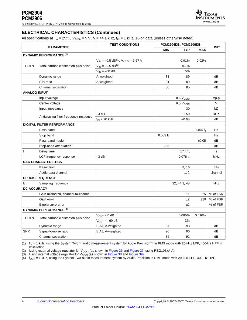
ELECTRICAL CHARACTERISTICS
PCM2904PCM2906
SLES042C–JUNE 2002–REVISED NOVEMBER 2007
All specifications at TA = 25°C, VBUS, = 5 V, fS = 44.1 kHz, fIN = 1 kHz, 16-bit data (unless otherwise noted)
PCM2904DB, PCM2906DBPARAMETER TEST CONDITIONS UNIT
MIN TYP MAXDIGITAL INPUT/OUTPUT
Host interface Apply USB Revision 1.1, full speedAudio data format USB isochronous data format
INPUT LOGICVIH
(1) 2 3.3VIL
(1) 0.8VIH
(2) (3) 2.52 3.3VIL
(2) (3) 0.9Input logic level Vdc
VIH(4) 2 5.25
VIL(4) 0.8
VIH(5) 2.52 5.25
VIL(5) 0.9
IIH(1) (2) (4) VIN = 3.3 V ±10IIL(1) (2) (4) VIN = 0 V ±10IIH(3) VIN = 3.3 V 50 80
Input logic current µAIIL(3) VIN = 0 V ±10IIH(5) VIN = 3.3 V 65 100IIL (5) VIN = 0 V ±10OUTPUT LOGICVOH
(1) 2.8VOL
(1) 0.3VOH
(6) IOH = –4 mA 2.8Output logic level Vdc
VOL(6) IOL = 4 mA 0.5
VOH(7) IOH = –2 mA 2.8
VOL(7) IOL = 2 mA 0.5
CLOCK FREQUENCYInput clock frequency, XTI 11.994 12 12.006 MHz
ADC CHARACTERISTICSResolution 8, 16 bitsAudio data channel 1, 2 channel
CLOCK FREQUENCY8, 11.025, 16, 22.05, 32,fs Sampling frequency kHz44.1, 48
DC ACCURACYGain mismatch, channel-to-channel ±1 ±5 % of FSRGain error ±2 ±10 % of FSRBipolar zero error ±0 % of FSR
(1) Pins 1, 2: D+, D–(2) Pin 21: XTI(3) Pins 5, 6, 7: HID0, HID1, HID2(4) Pins 8, 9: SEL0, SEL1(5) Pin 24: DIN(6) Pin 25: DOUT(7) Pin 28: SSPND
Copyright © 2002–2007, Texas Instruments Incorporated Submit Documentation Feedback 3
Product Folder Link(s): PCM2904 PCM2906
www.ti.com
ELECTRICAL CHARACTERISTICS (Continued)
PCM2904PCM2906SLES042C–JUNE 2002–REVISED NOVEMBER 2007
All specifications at TA = 25°C, VBUS, = 5 V, fS = 44.1 kHz, fIN = 1 kHz, 16-bit data (unless otherwise noted)
TEST CONDITIONS PCM2904DB, PCM2906DBPARAMETER UNIT
MIN TYP MAXDYNAMIC PERFORMANCE (1)
VIN = –0.5 dB (2), VCCCI = 3.67 V 0.01% 0.02%THD+N Total harmonic distortion plus noise VIN = –0.5 dB (3) 0.1%
VIN = –60 dB 5%Dynamic range A-weighted 81 89 dBS/N ratio A-weighted 81 89 dBChannel separation 80 85 dB
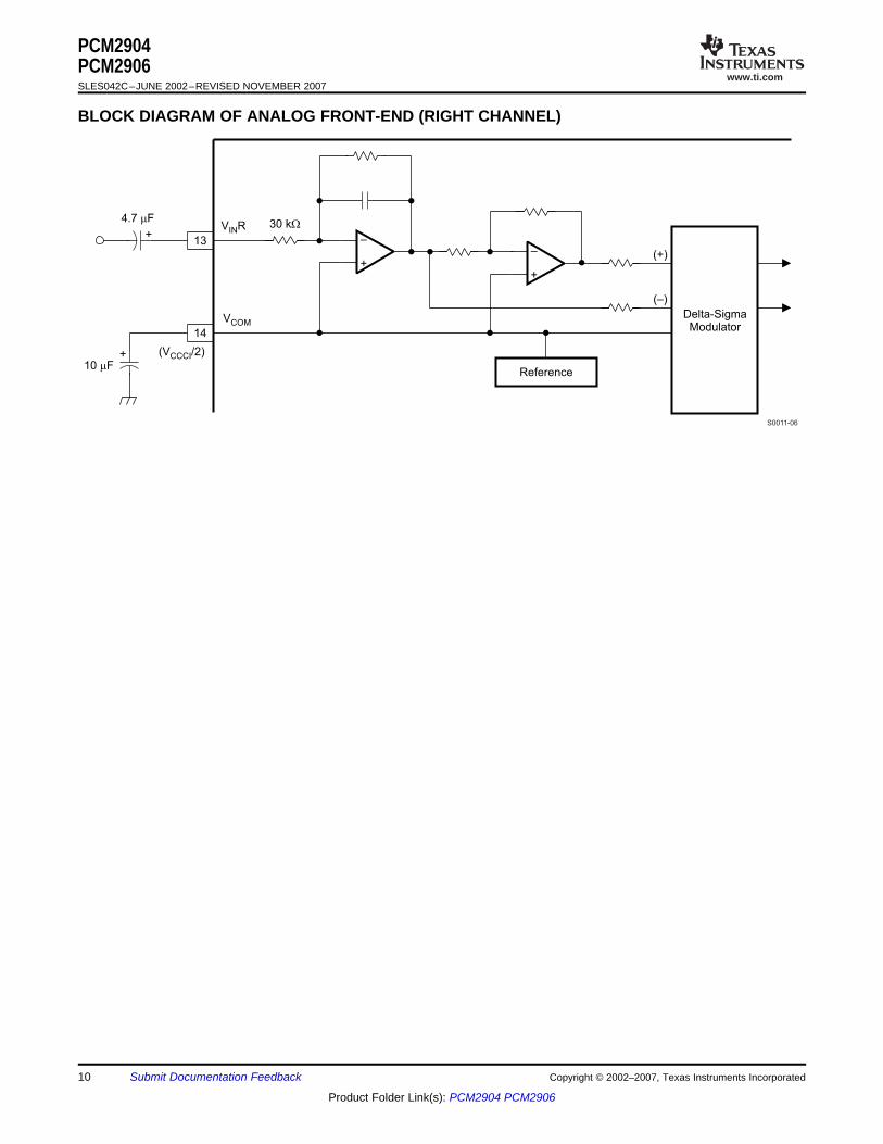
ANALOG INPUTInput voltage 0.6 VCCCI Vp-pCenter voltage 0.5 VCCCI VInput impedance 30 kΩ
–3 dB 150 kHzAntialiasing filter frequency response
fIN = 20 kHz –0.08 dBDIGITAL FILTER PERFORMANCE
Pass band 0.454 fs HzStop band 0.583 fs HzPass-band ripple ±0.05 dBStop-band attenuation –65 dB
td Delay time 17.4/fs sLCF frequency response –3 dB 0.078 fs MHz
DAC CHARACTERISTICSResolution 8, 16 bitsAudio data channel 1, 2 channel
CLOCK FREQUENCYfs Sampling frequency 32, 44.1, 48 kHzDC ACCURACY
Gain mismatch, channel-to-channel ±1 ±5 % of FSRGain error ±2 ±10 % of FSRBipolar zero error ±2 % of FSR
DYNAMIC PERFORMANCE (4)
VOUT = 0 dB 0.005% 0.016%THD+N Total harmonic distortion plus noise
VOUT = –60 dB 3%Dynamic range EIAJ, A-weighted 87 93 dB
SNR Signal-to-noise ratio EIAJ, A-weighted 90 96 dBChannel separation 86 92 dB
(1) fIN = 1 kHz, using the System Two™ audio measurement system by Audio Precision™ in RMS mode with 20-kHz LPF, 400-Hz HPF incalculation.
(2) Using external voltage regulator for VCCCI (as shown in Figure 36 and Figure 37, using REG103xA-A)(3) Using internal voltage regulator for VCCCI (as shown in Figure 38 and Figure 39)(4) fOUT = 1 kHz, using the System Two audio measurement system by Audio Precision in RMS mode with 20-kHz LPF, 400-Hz HPF.
4 Submit Documentation Feedback Copyright © 2002–2007, Texas Instruments Incorporated
Product Folder Link(s): PCM2904 PCM2906
www.ti.com
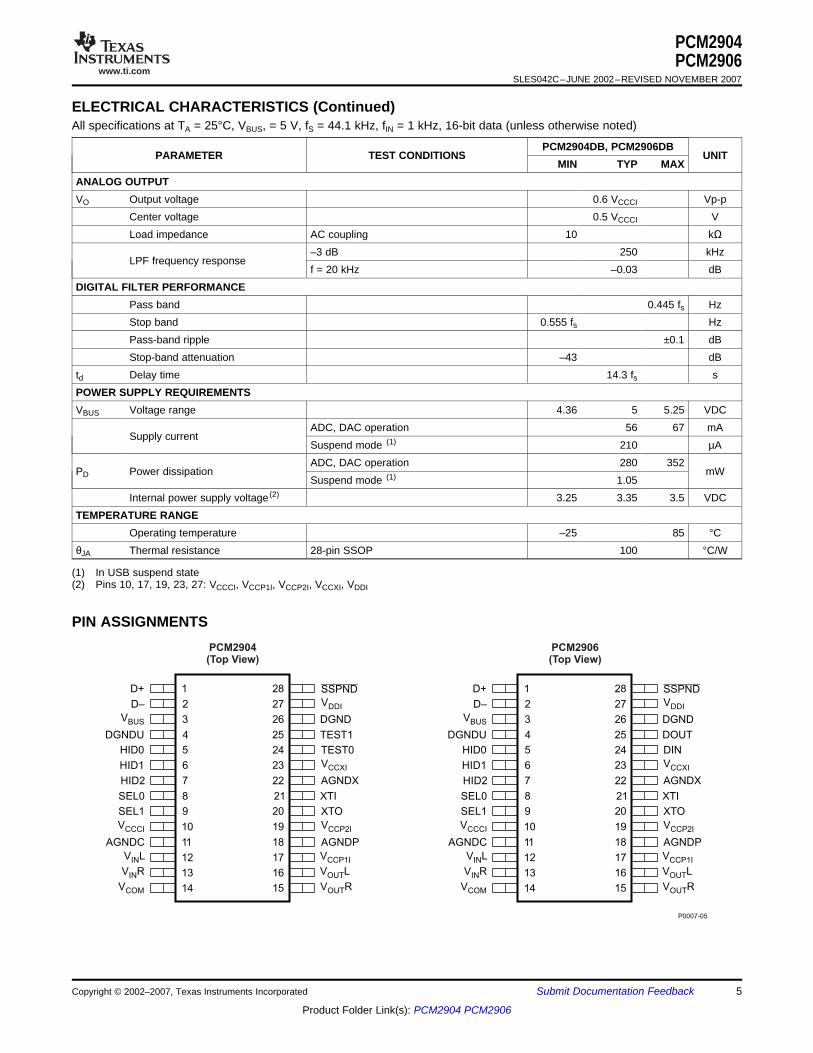
ELECTRICAL CHARACTERISTICS (Continued)
PIN ASSIGNMENTS
1
2
3
4
5
6
7
8
9
10
11
12
13
14
28
27
26
25
24
23
22
21
20
19
18
17
16
15
D+
D–
VBUS
DGNDU
HID0
HID1
HID2
SEL0
SEL1
VCCCI
AGNDC
V LIN
V RIN
VCOM
SSPND
TEST0
VCCXI
AGNDX
XTO
VCCP2I
DGND
VCCP1I
V LOUT
XTI
TEST1
VDDI
AGNDP
V ROUT
PCM2904(Top View)
1
2
3
4
5
6
7
8
9
10
11
12
13
14
28
27
26
25
24
23
22
21
20
19
18
17
16
15
D+
D–
VBUS
DGNDU
HID0
HID1
HID2
SEL0
SEL1
VCCCI
AGNDC
V LIN
V RIN
VCOM
SSPND
DIN
VCCXI
AGNDX
XTO
VCCP2I
DGND
VCCP1I
V LOUT
XTI
DOUT
VDDI
AGNDP
V ROUT
P0007-05
PCM2906(Top View)
PCM2904PCM2906
SLES042C–JUNE 2002–REVISED NOVEMBER 2007
All specifications at TA = 25°C, VBUS, = 5 V, fS = 44.1 kHz, fIN = 1 kHz, 16-bit data (unless otherwise noted)
PCM2904DB, PCM2906DBPARAMETER TEST CONDITIONS UNIT
MIN TYP MAXANALOG OUTPUTVO Output voltage 0.6 VCCCI Vp-p
Center voltage 0.5 VCCCI VLoad impedance AC coupling 10 kΩ
–3 dB 250 kHzLPF frequency response
f = 20 kHz –0.03 dBDIGITAL FILTER PERFORMANCE
Pass band 0.445 fs HzStop band 0.555 fs HzPass-band ripple ±0.1 dBStop-band attenuation –43 dB
td Delay time 14.3 fs sPOWER SUPPLY REQUIREMENTSVBUS Voltage range 4.36 5 5.25 VDC
ADC, DAC operation 56 67 mASupply current
Suspend mode (1) 210 µAADC, DAC operation 280 352
PD Power dissipation mWSuspend mode (1) 1.05
Internal power supply voltage (2) 3.25 3.35 3.5 VDCTEMPERATURE RANGE
Operating temperature –25 85 °CθJA Thermal resistance 28-pin SSOP 100 °C/W
(1) In USB suspend state(2) Pins 10, 17, 19, 23, 27: VCCCI, VCCP1I, VCCP2I, VCCXI, VDDI
Copyright © 2002–2007, Texas Instruments Incorporated Submit Documentation Feedback 5
Product Folder Link(s): PCM2904 PCM2906
www.ti.com
PCM2904PCM2906SLES042C–JUNE 2002–REVISED NOVEMBER 2007
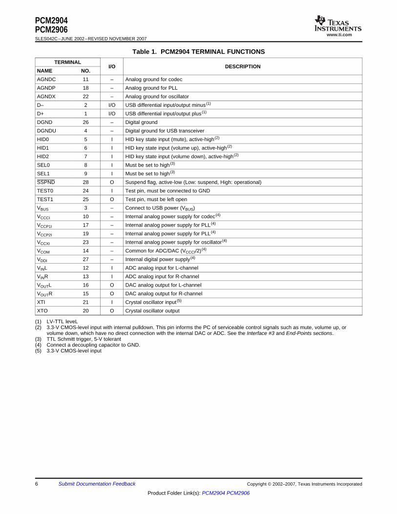
Table 1. PCM2904 TERMINAL FUNCTIONSTERMINAL
I/O DESCRIPTIONNAME NO.AGNDC 11 – Analog ground for codecAGNDP 18 – Analog ground for PLLAGNDX 22 – Analog ground for oscillatorD– 2 I/O USB differential input/output minus (1)
D+ 1 I/O USB differential input/output plus (1)
DGND 26 – Digital groundDGNDU 4 – Digital ground for USB transceiverHID0 5 I HID key state input (mute), active-high (2)
HID1 6 I HID key state input (volume up), active-high (2)
HID2 7 I HID key state input (volume down), active-high (2)
SEL0 8 I Must be set to high (3)
SEL1 9 I Must be set to high (3)
SSPND 28 O Suspend flag, active-low (Low: suspend, High: operational)TEST0 24 I Test pin, must be connected to GNDTEST1 25 O Test pin, must be left openVBUS 3 – Connect to USB power (VBUS)VCCCI 10 – Internal analog power supply for codec (4)
VCCP1I 17 – Internal analog power supply for PLL (4)
VCCP2I 19 – Internal analog power supply for PLL (4)
VCCXI 23 – Internal analog power supply for oscillator (4)
VCOM 14 – Common for ADC/DAC (VCCCI/2) (4)
VDDI 27 – Internal digital power supply (4)
VINL 12 I ADC analog input for L-channelVINR 13 I ADC analog input for R-channelVOUTL 16 O DAC analog output for L-channelVOUTR 15 O DAC analog output for R-channelXTI 21 I Crystal oscillator input (5)
XTO 20 O Crystal oscillator output
(1) LV-TTL leveL(2) 3.3-V CMOS-level input with internal pulldown. This pin informs the PC of serviceable control signals such as mute, volume up, or
volume down, which have no direct connection with the internal DAC or ADC. See the Interface #3 and End-Points sections.(3) TTL Schmitt trigger, 5-V tolerant(4) Connect a decoupling capacitor to GND.(5) 3.3-V CMOS-level input
6 Submit Documentation Feedback Copyright © 2002–2007, Texas Instruments Incorporated
Product Folder Link(s): PCM2904 PCM2906
www.ti.com
PCM2904PCM2906
SLES042C–JUNE 2002–REVISED NOVEMBER 2007
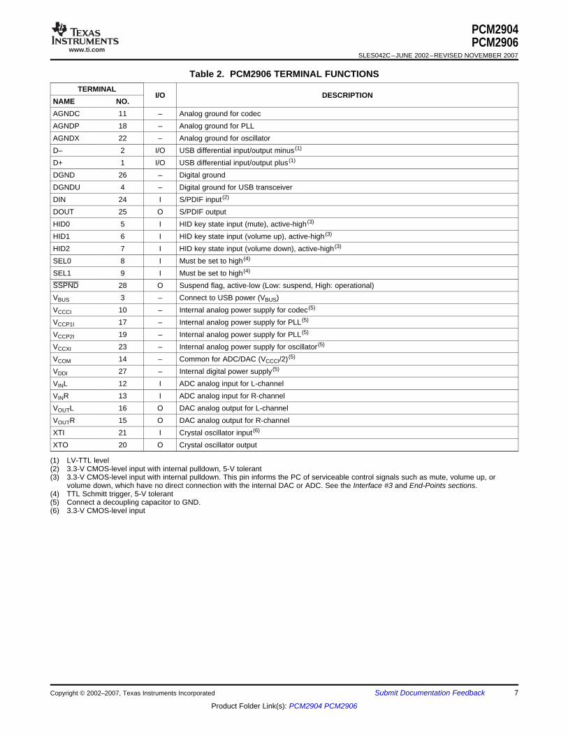
Table 2. PCM2906 TERMINAL FUNCTIONSTERMINAL
I/O DESCRIPTIONNAME NO.AGNDC 11 – Analog ground for codecAGNDP 18 – Analog ground for PLLAGNDX 22 – Analog ground for oscillatorD– 2 I/O USB differential input/output minus (1)
D+ 1 I/O USB differential input/output plus (1)
DGND 26 – Digital groundDGNDU 4 – Digital ground for USB transceiverDIN 24 I S/PDIF input (2)
DOUT 25 O S/PDIF outputHID0 5 I HID key state input (mute), active-high (3)
HID1 6 I HID key state input (volume up), active-high (3)
HID2 7 I HID key state input (volume down), active-high (3)
SEL0 8 I Must be set to high (4)
SEL1 9 I Must be set to high (4)
SSPND 28 O Suspend flag, active-low (Low: suspend, High: operational)VBUS 3 – Connect to USB power (VBUS)VCCCI 10 – Internal analog power supply for codec (5)
VCCP1I 17 – Internal analog power supply for PLL (5)
VCCP2I 19 – Internal analog power supply for PLL (5)
VCCXI 23 – Internal analog power supply for oscillator (5)
VCOM 14 – Common for ADC/DAC (VCCCI/2) (5)
VDDI 27 – Internal digital power supply (5)
VINL 12 I ADC analog input for L-channelVINR 13 I ADC analog input for R-channelVOUTL 16 O DAC analog output for L-channelVOUTR 15 O DAC analog output for R-channelXTI 21 I Crystal oscillator input (6)
XTO 20 O Crystal oscillator output
(1) LV-TTL level(2) 3.3-V CMOS-level input with internal pulldown, 5-V tolerant(3) 3.3-V CMOS-level input with internal pulldown. This pin informs the PC of serviceable control signals such as mute, volume up, or
volume down, which have no direct connection with the internal DAC or ADC. See the Interface #3 and End-Points sections.(4) TTL Schmitt trigger, 5-V tolerant(5) Connect a decoupling capacitor to GND.(6) 3.3-V CMOS-level input
Copyright © 2002–2007, Texas Instruments Incorporated Submit Documentation Feedback 7
Product Folder Link(s): PCM2904 PCM2906
www.ti.com
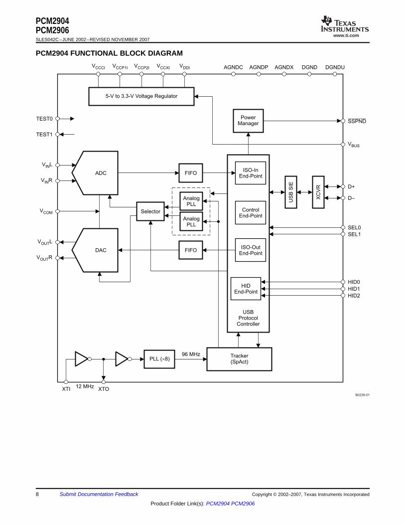
PCM2904 FUNCTIONAL BLOCK DIAGRAM
SSPND
TEST1
ADC
V LIN
V RIN
VCOM
FIFO
Selector
AnalogPLL
AnalogPLL
FIFO
US
B S
IE
XC
VR
DAC
V LOUT
V ROUT
XTI XTO12 MHz
PLL ( 8)´
96 MHz Tracker(SpAct)
USBProtocol
Controller
PowerManager
ISO-InEnd-Point
ControlEnd-Point
ISO-OutEnd-Point
HIDEnd-Point
D+
D–
SEL0
SEL1
HID0
HID1
HID2
VBUS
5-V to 3.3-V Voltage Regulator
VCCCI VCCP1I VCCP2I VCCXI VDDI DGNDUDGNDAGNDXAGNDPAGNDC
B0238-01
TEST0
PCM2904PCM2906SLES042C–JUNE 2002–REVISED NOVEMBER 2007
8 Submit Documentation Feedback Copyright © 2002–2007, Texas Instruments Incorporated
Product Folder Link(s): PCM2904 PCM2906
www.ti.com
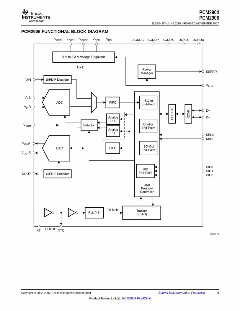
PCM2906 FUNCTIONAL BLOCK DIAGRAM
SSPND
S/PDIF DecoderDIN
Lock
ADC
V LIN
V RIN
VCOM
FIFO
Selector
AnalogPLL
AnalogPLL
FIFO
US
B S
IE
XC
VR
DAC
V LOUT
V ROUT
S/PDIF EncoderDOUT
XTI XTO12 MHz
PLL ( 8)´
96 MHz Tracker(SpAct)
USBProtocol
Controller
PowerManager
ISO-InEnd-Point
ControlEnd-Point
ISO-OutEnd-Point
HIDEnd-Point
D+
D–
SEL0
SEL1
HID0
HID1
HID2
VBUS
5-V to 3.3-V Voltage Regulator
VCCCI VCCP1I VCCP2I VCCXI VDDI DGNDUDGNDAGNDXAGNDPAGNDC
B0239-01
PCM2904PCM2906
SLES042C–JUNE 2002–REVISED NOVEMBER 2007
Copyright © 2002–2007, Texas Instruments Incorporated Submit Documentation Feedback 9
Product Folder Link(s): PCM2904 PCM2906
www.ti.com
BLOCK DIAGRAM OF ANALOG FRONT-END (RIGHT CHANNEL)
V RIN
13
14
VCOM
4.7 Fm30 kW
++
––
Delta-SigmaModulator
(+)
(–)
Reference
(V /2)CCCI
10 Fm
+
+
S0011-06
PCM2904PCM2906SLES042C–JUNE 2002–REVISED NOVEMBER 2007
10 Submit Documentation Feedback Copyright © 2002–2007, Texas Instruments Incorporated
Product Folder Link(s): PCM2904 PCM2906
www.ti.com
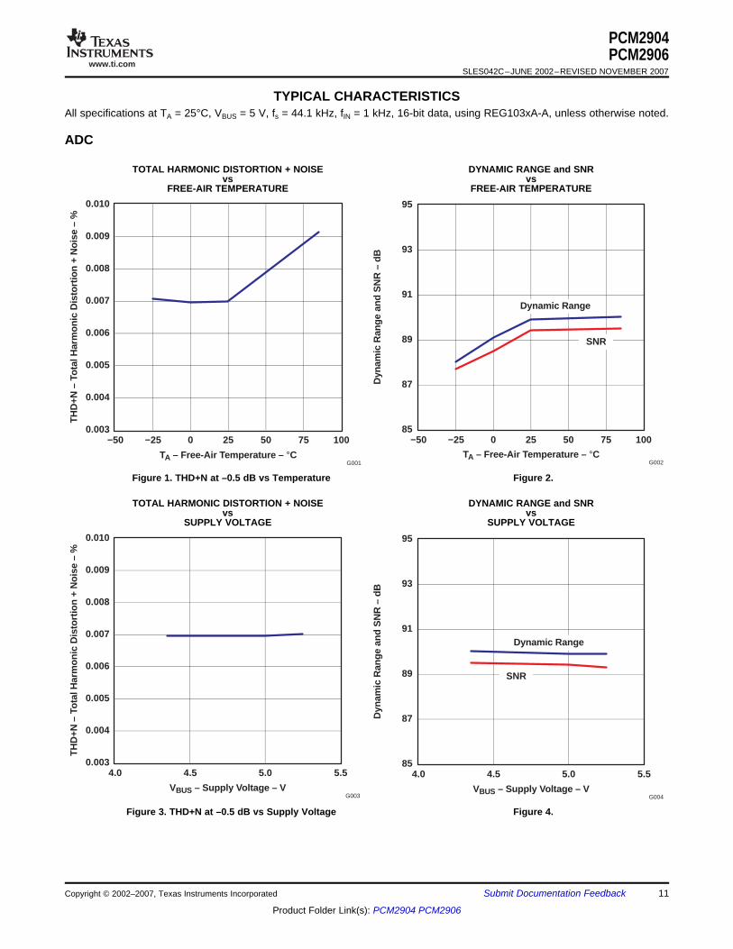
TYPICAL CHARACTERISTICS
ADC
85
87
89
91
93
95
−50 −25 0 25 50 75 100
TA – Free-Air T emperature – °C
Dyn
amic
Ran
ge a
nd S
NR
– d
B
SNR
Dynamic Range
G002
0.003
0.004
0.005
0.006
0.007
0.008
0.009
0.010
−50 −25 0 25 50 75 100
TA – Free-Air T emperature – °C
TH
D+N
– T
otal
Har
mon
ic D
isto
rtion
+ N
oise
– %
G001
0.003
0.004
0.005
0.006
0.007
0.008
0.009
0.010
4.0 4.5 5.0 5.5
VBUS – Supply Voltage – V
TH
D+N
– T
ota
l Har
mo
nic
Dis
tort
ion
+ N
ois
e –
%
G003
85
87
89
91
93
95
4.0 4.5 5.0 5.5
VBUS – Supply Voltage – V
Dyn
amic
Ran
ge
and
SN
R –
dB
SNR
Dynamic Range
G004
PCM2904PCM2906
SLES042C–JUNE 2002–REVISED NOVEMBER 2007
All specifications at TA = 25°C, VBUS = 5 V, fs = 44.1 kHz, fIN = 1 kHz, 16-bit data, using REG103xA-A, unless otherwise noted.
TOTAL HARMONIC DISTORTION + NOISE DYNAMIC RANGE and SNRvs vs
FREE-AIR TEMPERATURE FREE-AIR TEMPERATURE
Figure 1. THD+N at –0.5 dB vs Temperature Figure 2.
TOTAL HARMONIC DISTORTION + NOISE DYNAMIC RANGE and SNRvs vs
SUPPLY VOLTAGE SUPPLY VOLTAGE
Figure 3. THD+N at –0.5 dB vs Supply Voltage Figure 4.
Copyright © 2002–2007, Texas Instruments Incorporated Submit Documentation Feedback 11
Product Folder Link(s): PCM2904 PCM2906
www.ti.com
0.003
0.004
0.005
0.006
0.007
0.008
0.009
0.010
30 35 40 45 50
fS – Sampling Frequency – kHz
TH
D+N
– T
ota
l Har
mo
nic
Dis
tort
ion
+ N
ois
e –
%
G005
85
87
89
91
93
95
30 35 40 45 50
fS – Sampling Frequency – kHz
Dyn
amic
Ran
ge
and
SN
R –
dB
SNR
Dynamic Range
G006
DAC
90
91
92
93
94
95
96
97
98
−50 −25 0 25 50 75 100
TA – Free-Air T emperature – °C
Dyn
amic
Ran
ge a
nd S
NR
– d
B
SNR
Dynamic Range
G008
0.003
0.004
0.005
0.006
0.007
0.008
−50 −25 0 25 50 75 100
TA – Free-Air T emperature – °C
TH
D+N
– T
otal
Har
mon
ic D
isto
rtion
+ N
oise
– %
G007
PCM2904PCM2906SLES042C–JUNE 2002–REVISED NOVEMBER 2007
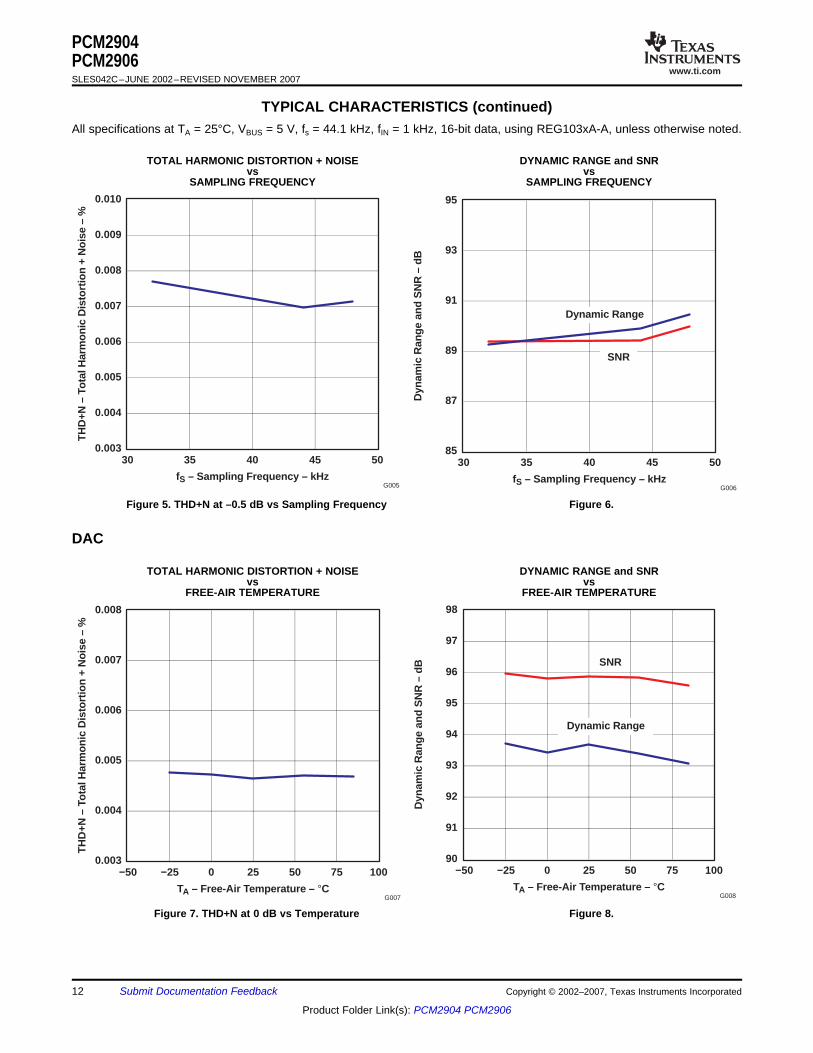
TYPICAL CHARACTERISTICS (continued)All specifications at TA = 25°C, VBUS = 5 V, fs = 44.1 kHz, fIN = 1 kHz, 16-bit data, using REG103xA-A, unless otherwise noted.
TOTAL HARMONIC DISTORTION + NOISE DYNAMIC RANGE and SNRvs vs
SAMPLING FREQUENCY SAMPLING FREQUENCY
Figure 5. THD+N at –0.5 dB vs Sampling Frequency Figure 6.
TOTAL HARMONIC DISTORTION + NOISE DYNAMIC RANGE and SNRvs vs
FREE-AIR TEMPERATURE FREE-AIR TEMPERATURE
Figure 7. THD+N at 0 dB vs Temperature Figure 8.
12 Submit Documentation Feedback Copyright © 2002–2007, Texas Instruments Incorporated
Product Folder Link(s): PCM2904 PCM2906
www.ti.com
0.003
0.004
0.005
0.006
0.007
0.008
4.0 4.5 5.0 5.5
VBUS – Supply Voltage – V
TH
D+N
– T
ota
l Har
mo
nic
Dis
tort
ion
+ N
ois
e –
%
G009
90
91
92
93
94
95
96
97
98
4.0 4.5 5.0 5.5
VBUS – Supply Voltage – V
Dyn
amic
Ran
ge
and
SN
R –
dB SNR
Dynamic Range
G010
90
91
92
93
94
95
96
97
98
30 35 40 45 50
fS – Sampling Frequency – kHz
Dyn
amic
Ran
ge
and
SN
R –
dB
SNR
Dynamic Range
G012
0.003
0.004
0.005
0.006
0.007
0.008
30 35 40 45 50
fS – Sampling Frequency – kHz
TH
D+N
– T
ota
l Har
mo
nic
Dis
tort
ion
+ N
ois
e –
%
G011
PCM2904PCM2906
SLES042C–JUNE 2002–REVISED NOVEMBER 2007
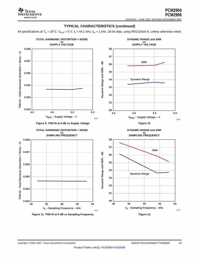
TYPICAL CHARACTERISTICS (continued)All specifications at TA = 25°C, VBUS = 5 V, fs = 44.1 kHz, fIN = 1 kHz, 16-bit data, using REG103xA-A, unless otherwise noted.
TOTAL HARMONIC DISTORTION + NOISE DYNAMIC RANGE and SNRvs vs
SUPPLY VOLTAGE SUPPLY VOLTAGE
Figure 9. THD+N at 0 dB vs Supply Voltage Figure 10.
TOTAL HARMONIC DISTORTION + NOISE DYNAMIC RANGE and SNRvs vs
SAMPLING FREQUENCY SAMPLING FREQUENCY
Figure 11. THD+N at 0 dB vs Sampling Frequency Figure 12.
Copyright © 2002–2007, Texas Instruments Incorporated Submit Documentation Feedback 13
Product Folder Link(s): PCM2904 PCM2906
www.ti.com
SUPPLY CURRENT
0.20
0.22
0.24
0.26
0.28
0.30
I CC
– S
usp
end
Su
pp
ly C
urr
ent –
mA
20
30
40
50
60
70
4.00 4.25 4.50 4.75 5.00 5.25 5.50
VBUS – Supply Voltage – V
I CC
– O
per
atio
nal
Su
pp
ly C
urr
ent –
mA
Operational
Suspend
G013
20
30
40
50
60
70
30 35 40 45 50
fS – Sampling Frequency – kHz
I CC
– O
per
atio
nal
Su
pp
ly C
urr
ent –
mA
G014
0.10
0.15
0.20
0.25
0.30
0.35
0.40
−40 −20 0 20 40 60 80 100
TA – Free-Air T emperature – °C
I CC
– S
uspe
nd S
uppl
y C
urre
nt –
mA
USB Spec Limit for Device (0.3 mA)
G015
PCM2904PCM2906SLES042C–JUNE 2002–REVISED NOVEMBER 2007
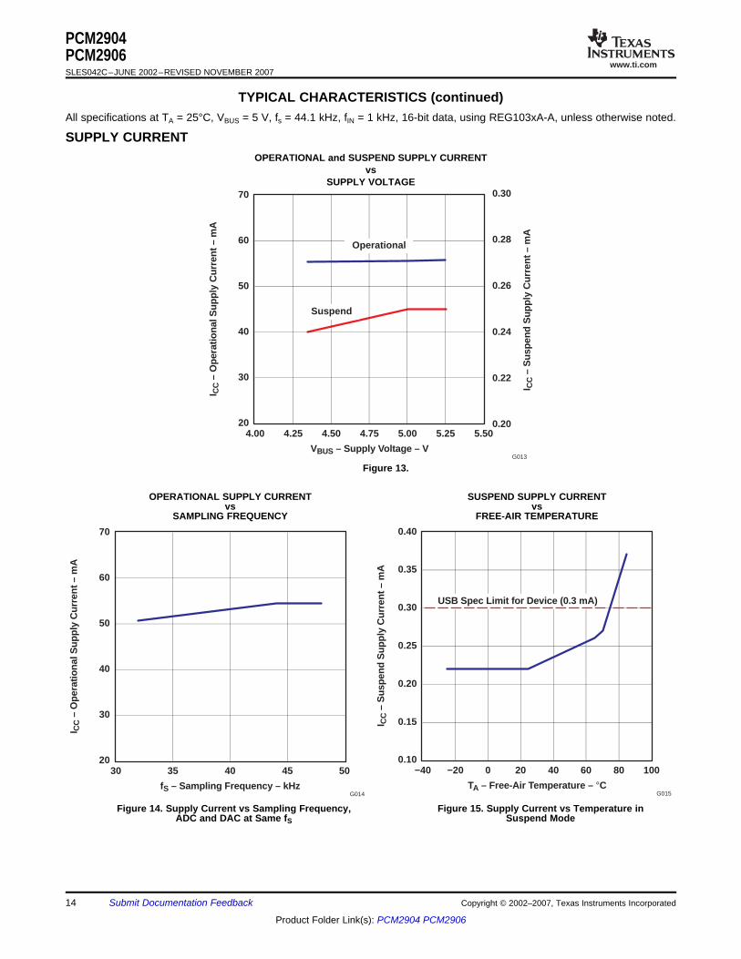
TYPICAL CHARACTERISTICS (continued)All specifications at TA = 25°C, VBUS = 5 V, fs = 44.1 kHz, fIN = 1 kHz, 16-bit data, using REG103xA-A, unless otherwise noted.
OPERATIONAL and SUSPEND SUPPLY CURRENTvs
SUPPLY VOLTAGE
Figure 13.
OPERATIONAL SUPPLY CURRENT SUSPEND SUPPLY CURRENTvs vs
SAMPLING FREQUENCY FREE-AIR TEMPERATURE
Figure 14. Supply Current vs Sampling Frequency, Figure 15. Supply Current vs Temperature inADC and DAC at Same fS Suspend Mode
14 Submit Documentation Feedback Copyright © 2002–2007, Texas Instruments Incorporated
Product Folder Link(s): PCM2904 PCM2906
www.ti.com
ADC DIGITAL DECIMATION FILTER FREQUENCY RESPONSE
−160
−140
−120
−100
−80
−60
−40
−20
0
0 8 16 24 32
Am
plitu
de –
dB
Frequency [ fS]G016
Frequency [ fS]
−100
−90
−80
−70
−60
−50
−40
−30
−20
−10
0
0.0 0.2 0.4 0.6 0.8 1.0
Am
plitu
de –
dB
G017
Frequency [ fS]
−0.8
−0.6
−0.4
−0.2
0.0
0.2
0.0 0.1 0.2 0.3 0.4 0.5
Am
plitu
de –
dB
0.0
G018Frequency [ fS]
−20
−16
−12
−8
−4
0
0.46 0.48 0.50 0.52 0.54
Am
plitu
de –
dB
G019
PCM2904PCM2906
SLES042C–JUNE 2002–REVISED NOVEMBER 2007
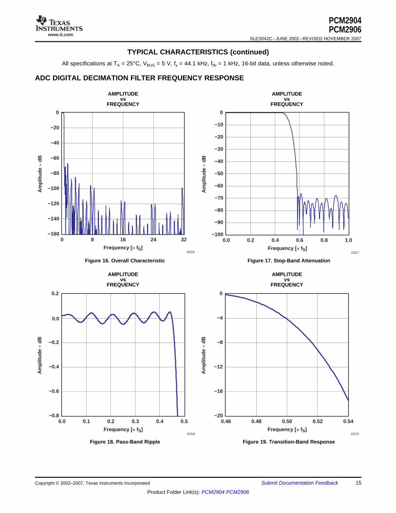
TYPICAL CHARACTERISTICS (continued)All specifications at TA = 25°C, VBUS = 5 V, fs = 44.1 kHz, fIN = 1 kHz, 16-bit data, unless otherwise noted.
AMPLITUDE AMPLITUDEvs vs
FREQUENCY FREQUENCY
Figure 16. Overall Characteristic Figure 17. Stop-Band Attenuation
AMPLITUDE AMPLITUDEvs vs
FREQUENCY FREQUENCY
Figure 18. Pass-Band Ripple Figure 19. Transition-Band Response
Copyright © 2002–2007, Texas Instruments Incorporated Submit Documentation Feedback 15
Product Folder Link(s): PCM2904 PCM2906
www.ti.com
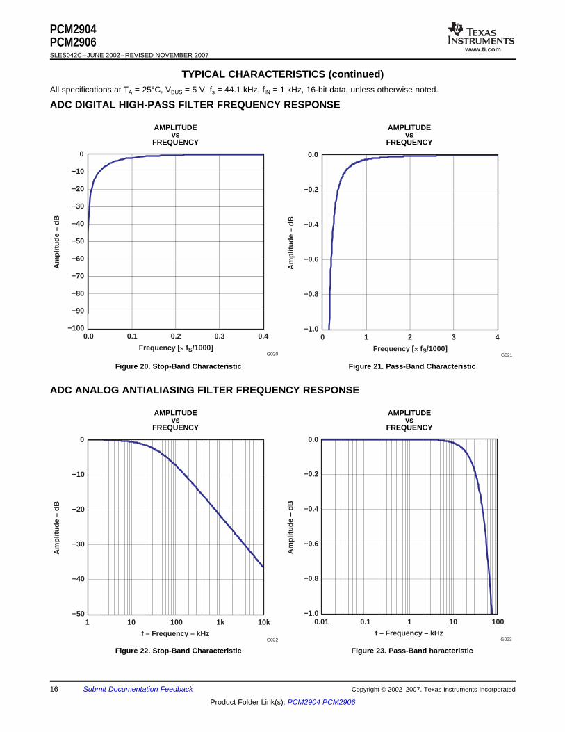
ADC DIGITAL HIGH-PASS FILTER FREQUENCY RESPONSE
Frequency [ fS/1000]
−100
−90
−80
−70
−60
−50
−40
−30
−20
−10
0
0.0 0.1 0.2 0.3 0.4
Am
plitu
de –
dB
G020Frequency [ fS/1000]
−1.0
−0.8
−0.6
−0.4
−0.2
0.0
0 1 2 3 4
Am
plitu
de –
dB
G021
ADC ANALOG ANTIALIASING FILTER FREQUENCY RESPONSE
−50
−40
−30
−20
−10
0
f – Frequency – kHz
Am
plitu
de –
dB
1 100 1k 10k10
G022
−1.0
−0.8
−0.6
−0.4
−0.2
0.0
f – Frequency – kHz
Am
plitu
de –
dB
0.01 1 10 1000.1
0.0
G023
PCM2904PCM2906SLES042C–JUNE 2002–REVISED NOVEMBER 2007
TYPICAL CHARACTERISTICS (continued)All specifications at TA = 25°C, VBUS = 5 V, fs = 44.1 kHz, fIN = 1 kHz, 16-bit data, unless otherwise noted.
AMPLITUDE AMPLITUDEvs vs
FREQUENCY FREQUENCY
Figure 20. Stop-Band Characteristic Figure 21. Pass-Band Characteristic
AMPLITUDE AMPLITUDEvs vs
FREQUENCY FREQUENCY
Figure 22. Stop-Band Characteristic Figure 23. Pass-Band haracteristic
16 Submit Documentation Feedback Copyright © 2002–2007, Texas Instruments Incorporated
Product Folder Link(s): PCM2904 PCM2906
www.ti.com
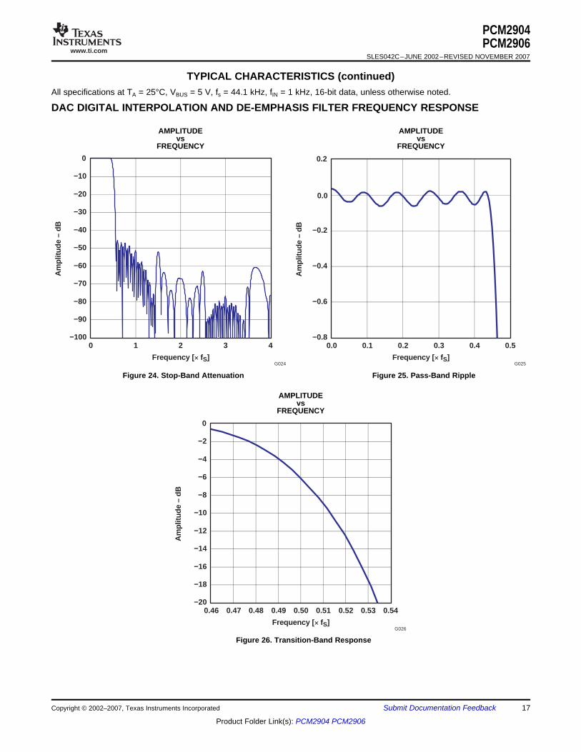
DAC DIGITAL INTERPOLATION AND DE-EMPHASIS FILTER FREQUENCY RESPONSE
Frequency [ fS]
−100
−90
−80
−70
−60
−50
−40
−30
−20
−10
0
0 1 2 3 4
Am
plitu
de –
dB
G024Frequency [ fS]
−0.8
−0.6
−0.4
−0.2
0.0
0.2
0.0 0.1 0.2 0.3 0.4 0.5
Am
plitu
de –
dB
0.0
G025
Frequency [ fS]
−20
−18
−16
−14
−12
−10
−8
−6
−4
−2
0
0.46 0.47 0.48 0.49 0.50 0.51 0.52 0.53 0.54
Am
plitu
de –
dB
G026
PCM2904PCM2906
SLES042C–JUNE 2002–REVISED NOVEMBER 2007
TYPICAL CHARACTERISTICS (continued)All specifications at TA = 25°C, VBUS = 5 V, fs = 44.1 kHz, fIN = 1 kHz, 16-bit data, unless otherwise noted.
AMPLITUDE AMPLITUDEvs vs
FREQUENCY FREQUENCY
Figure 24. Stop-Band Attenuation Figure 25. Pass-Band Ripple
AMPLITUDEvs
FREQUENCY
Figure 26. Transition-Band Response
Copyright © 2002–2007, Texas Instruments Incorporated Submit Documentation Feedback 17
Product Folder Link(s): PCM2904 PCM2906
www.ti.com
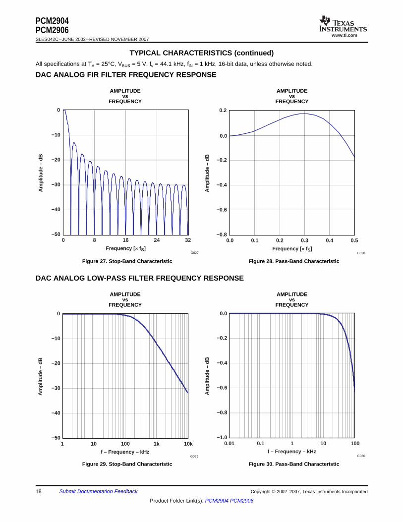
DAC ANALOG FIR FILTER FREQUENCY RESPONSE
−50
−40
−30
−20
−10
0
0 8 16 24 32
Frequency [ fS]
Am
plitu
de –
dB
G027
−0.8
−0.6
−0.4
−0.2
0.0
0.2
0.0 0.1 0.2 0.3 0.4 0.5
Frequency [ fS]
Am
plitu
de –
dB
0.0
G028
DAC ANALOG LOW-PASS FILTER FREQUENCY RESPONSE
−50
−40
−30
−20
−10
0
f – Frequency – kHz
Am
plitu
de –
dB
1 100 1k 10k10
G029
−1.0
−0.8
−0.6
−0.4
−0.2
0.0
f – Frequency – kHz
Am
plitu
de –
dB
0.01 1 10 1000.1
0.0
G030
PCM2904PCM2906SLES042C–JUNE 2002–REVISED NOVEMBER 2007
TYPICAL CHARACTERISTICS (continued)All specifications at TA = 25°C, VBUS = 5 V, fs = 44.1 kHz, fIN = 1 kHz, 16-bit data, unless otherwise noted.
AMPLITUDE AMPLITUDEvs vs
FREQUENCY FREQUENCY
Figure 27. Stop-Band Characteristic Figure 28. Pass-Band Characteristic
AMPLITUDE AMPLITUDEvs vs
FREQUENCY FREQUENCY
Figure 29. Stop-Band Characteristic Figure 30. Pass-Band Characteristic
18 Submit Documentation Feedback Copyright © 2002–2007, Texas Instruments Incorporated
Product Folder Link(s): PCM2904 PCM2906
www.ti.com
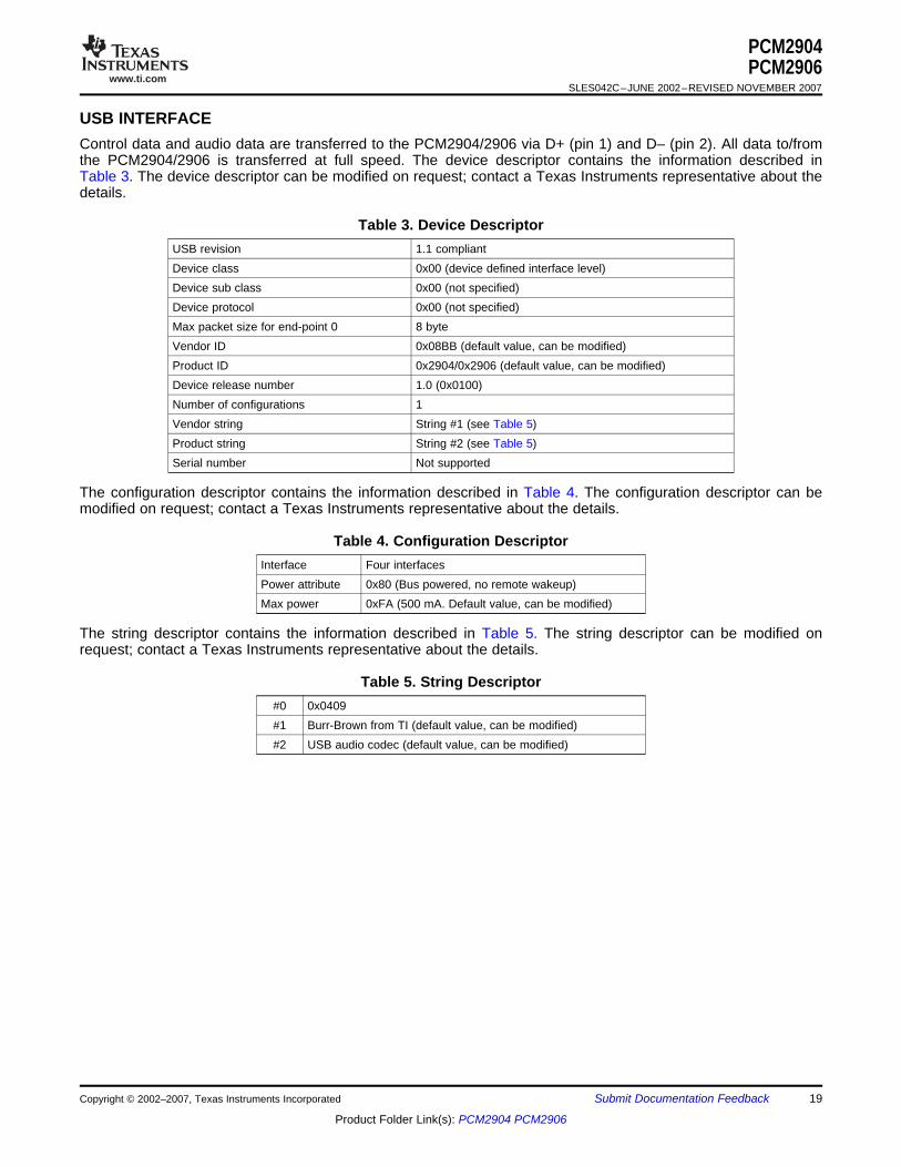
USB INTERFACE
PCM2904PCM2906
SLES042C–JUNE 2002–REVISED NOVEMBER 2007
Control data and audio data are transferred to the PCM2904/2906 via D+ (pin 1) and D– (pin 2). All data to/fromthe PCM2904/2906 is transferred at full speed. The device descriptor contains the information described inTable 3. The device descriptor can be modified on request; contact a Texas Instruments representative about thedetails.
Table 3. Device DescriptorUSB revision 1.1 compliantDevice class 0x00 (device defined interface level)Device sub class 0x00 (not specified)Device protocol 0x00 (not specified)Max packet size for end-point 0 8 byteVendor ID 0x08BB (default value, can be modified)Product ID 0x2904/0x2906 (default value, can be modified)Device release number 1.0 (0x0100)Number of configurations 1Vendor string String #1 (see Table 5)Product string String #2 (see Table 5)Serial number Not supported
The configuration descriptor contains the information described in Table 4. The configuration descriptor can bemodified on request; contact a Texas Instruments representative about the details.
Table 4. Configuration DescriptorInterface Four interfacesPower attribute 0x80 (Bus powered, no remote wakeup)Max power 0xFA (500 mA. Default value, can be modified)
The string descriptor contains the information described in Table 5. The string descriptor can be modified onrequest; contact a Texas Instruments representative about the details.
Table 5. String Descriptor#0 0x0409#1 Burr-Brown from TI (default value, can be modified)#2 USB audio codec (default value, can be modified)
Copyright © 2002–2007, Texas Instruments Incorporated Submit Documentation Feedback 19
Product Folder Link(s): PCM2904 PCM2906

www.ti.com
DEVICE CONFIGURATION
Analog Out
Analog In
Default End-Point
End-Point #2(IF #1)
Audio Streaming Interface
End-Point #0
End-Point #4(IF #2)
Audio Streaming Interface
End-Point #5(IF #3)
HID Interface
ITTID1
FU
UID3
OTTID5
OTTID2
ITTID4
Standard Audio Control Interface (IF #0)
PCM2904/2906
M0024-02
PCM2904PCM2906SLES042C–JUNE 2002–REVISED NOVEMBER 2007
Figure 31 illustrates the USB audio function topology. The PCM2904/2906 has four interfaces. Each interface isconstructed by alternative settings.
Figure 31. USB Audio Function Topology
20 Submit Documentation Feedback Copyright © 2002–2007, Texas Instruments Incorporated
Product Folder Link(s): PCM2904 PCM2906
www.ti.com
Interface #0
Interface #1
PCM2904PCM2906
SLES042C–JUNE 2002–REVISED NOVEMBER 2007
Interface #0 is the control interface. Alternative setting #0 is the only possible setting for interface #0. Alternativesetting #0 describes the standard audio control interface. The audio control interface is constructed by a terminal.The PCM2904/2906 has the following five terminals.• Input terminal (IT #1) for isochronous-out stream• Output terminal (OT #2) for audio analog output• Feature unit (FU #3) for DAC digital attenuator• Input terminal (IT #4) for audio analog input• Output terminal (OT #5) for isochronous-in stream
Input terminal #1 is defined as a USB stream (terminal type 0x0101). Input terminal #1 can accept 2-channelaudio streams consisting of left and right channels. Output terminal #2 is defined as a speaker (terminal type0x0301). Input terminal #4 is defined as a microphone (terminal type 0x0201). Output terminal #5 is defined as aUSB stream (terminal type 0x0101). Output terminal #5 can generate 2-channel audio streams consisting of leftand right channels. Feature unit #3 supports the following sound control features.• Volume control• Mute control
The built-in digital volume controller can be manipulated by an audio-class-specific request from 0 dB to –64 dBin steps of 1 dB. Each channel can be set for different values. The master volume control is not supported. Arequest to the master volume is stalled and ignored. The built-in digital mute controller can be manipulated byaudio-class-specific request. A master mute control request is acceptable. A request to an individual channel isstalled and ignored.
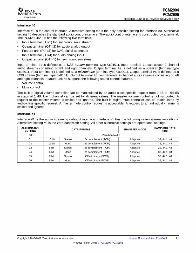
Interface #1 is the audio streaming data-out interface. Interface #1 has the following seven alternative settings.Alternative setting #0 is the zero-bandwidth setting. All other alternative settings are operational settings.
ALTERNATIVE SAMPLING RATEDATA FORMAT TRANSFER MODESETTING (kHz)00 Zero bandwidth01 16 bit Stereo 2s complement (PCM) Adaptive 32, 44.1, 4802 16 bit Mono 2s complement (PCM) Adaptive 32, 44.1, 4803 8 bit Stereo 2s complement (PCM) Adaptive 32, 44.1, 4804 8 bit Mono 2s complement (PCM) Adaptive 32, 44.1, 4805 8 bit Stereo Offset binary (PCM8) Adaptive 32, 44.1, 4806 8 bit Mono Offset binary (PCM8) Adaptive 32, 44.1, 48
Copyright © 2002–2007, Texas Instruments Incorporated Submit Documentation Feedback 21
Product Folder Link(s): PCM2904 PCM2906
www.ti.com
Interface #2
Interface #3
End-Points
PCM2904PCM2906SLES042C–JUNE 2002–REVISED NOVEMBER 2007
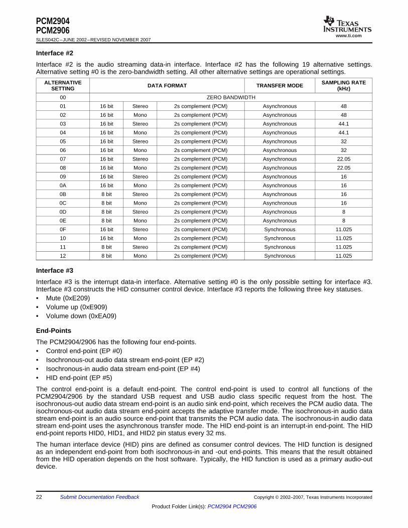
Interface #2 is the audio streaming data-in interface. Interface #2 has the following 19 alternative settings.Alternative setting #0 is the zero-bandwidth setting. All other alternative settings are operational settings.
ALTERNATIVE SAMPLING RATEDATA FORMAT TRANSFER MODESETTING (kHz)00 ZERO BANDWIDTH01 16 bit Stereo 2s complement (PCM) Asynchronous 4802 16 bit Mono 2s complement (PCM) Asynchronous 4803 16 bit Stereo 2s complement (PCM) Asynchronous 44.104 16 bit Mono 2s complement (PCM) Asynchronous 44.105 16 bit Stereo 2s complement (PCM) Asynchronous 3206 16 bit Mono 2s complement (PCM) Asynchronous 3207 16 bit Stereo 2s complement (PCM) Asynchronous 22.0508 16 bit Mono 2s complement (PCM) Asynchronous 22.0509 16 bit Stereo 2s complement (PCM) Asynchronous 160A 16 bit Mono 2s complement (PCM) Asynchronous 160B 8 bit Stereo 2s complement (PCM) Asynchronous 160C 8 bit Mono 2s complement (PCM) Asynchronous 160D 8 bit Stereo 2s complement (PCM) Asynchronous 80E 8 bit Mono 2s complement (PCM) Asynchronous 80F 16 bit Stereo 2s complement (PCM) Synchronous 11.02510 16 bit Mono 2s complement (PCM) Synchronous 11.02511 8 bit Stereo 2s complement (PCM) Synchronous 11.02512 8 bit Mono 2s complement (PCM) Synchronous 11.025
Interface #3 is the interrupt data-in interface. Alternative setting #0 is the only possible setting for interface #3.Interface #3 constructs the HID consumer control device. Interface #3 reports the following three key statuses.• Mute (0xE209)• Volume up (0xE909)• Volume down (0xEA09)
The PCM2904/2906 has the following four end-points.• Control end-point (EP #0)• Isochronous-out audio data stream end-point (EP #2)• Isochronous-in audio data stream end-point (EP #4)• HID end-point (EP #5)
The control end-point is a default end-point. The control end-point is used to control all functions of thePCM2904/2906 by the standard USB request and USB audio class specific request from the host. Theisochronous-out audio data stream end-point is an audio sink end-point, which receives the PCM audio data. Theisochronous-out audio data stream end-point accepts the adaptive transfer mode. The isochronous-in audio datastream end-point is an audio source end-point that transmits the PCM audio data. The isochronous-in audio datastream end-point uses the asynchronous transfer mode. The HID end-point is an interrupt-in end-point. The HIDend-point reports HID0, HID1, and HID2 pin status every 32 ms.
The human interface device (HID) pins are defined as consumer control devices. The HID function is designedas an independent end-point from both isochronous-in and -out end-points. This means that the result obtainedfrom the HID operation depends on the host software. Typically, the HID function is used as a primary audio-outdevice.
22 Submit Documentation Feedback Copyright © 2002–2007, Texas Instruments Incorporated
Product Folder Link(s): PCM2904 PCM2906
www.ti.com
Clock and Reset
Digital Audio Interface (PCM2906)
Supported Input Data (PCM2906)
Channel Status Information (PCM2906)
Copyright Management (PCM2906)
PCM2904PCM2906
SLES042C–JUNE 2002–REVISED NOVEMBER 2007
The PCM2904/2906 requires a 12-MHz (±500 ppm) clock for the USB and audio functions. The clock can begenerated by a built-in oscillator with a 12-MHz crystal resonator. The 12-MHz crystal resonator must beconnected to XTI (pin 21) and XTO (pin 20) with one high-value (1-MΩ) resistor and two small capacitors, thecapacitance of which depends on the load capacitance of the crystal resonator. An external clock can besupplied to XTI (pin 21). If an external clock is used, XTO (pin 20) must be left open. Because there is no clockdisabling signal, use of the external clock supply is not recommended. SSPND (pin 28) is unable to use clockdisabling.
The PCM2904/2906 has an internal power-on reset circuit, which is triggered automatically when VBUS (pin 3)exceeds 2.5 V typical (2.7 V to 2.2 V). About 700 µs is required until internal reset release.
The PCM2906 employs S/PDIF for both input and output. Isochronous-out data from the host is encoded to theS/PDIF output and the DAC analog output. Input data is selected from either the S/PDIF or ADC analog input.When the device detects S/PDIF input and successfully locks the received data, the isochronous-in transfer datasource automatically selected is S/PDIF; otherwise, the data source selected is the ADC analog input.
The following data formats are accepted by S/PDIF for input and output. All other data formats are unusable asS/PDIF.• 48-kHz 16-bit stereo• 44.1-kHz 16-bit stereo• 32-kHz 16-bit stereo
Mismatch between the input data format and the host command may cause unexpected results, with thefollowing exceptions:• Recording in monaural format from stereo data input at the same data rate• Recording in 8-bit format from 16-bit data input at the same data rate
A combination of the two foregoing conditions is not accepted.
For playback, all possible data-rate sources are converted to the 16-bit stereo format at the same source datarate.
The channel status information is fixed as consumer application, PCM mode, copyright, and digital/digitalconverter. All other bits are fixed as 0s except for the sample frequency, which is set automatically according tothe data received through the USB.
Isochronous-in data is affected by the serial copy management system (SCMS). When the control bit indicatesthat the received digital audio data is original, the input digital audio data is transferred to the host. If the data isindicated as first generation or higher, the transferred data is routed to the analog input.
Digital audio data output is always encoded as original with SCMS control.
The implementation of this feature is optional. It is the designer's responsibility to determine whether toimplement this feature in a product or not.
Copyright © 2002–2007, Texas Instruments Incorporated Submit Documentation Feedback 23
Product Folder Link(s): PCM2904 PCM2906
www.ti.com
INTERFACE SEQUENCE
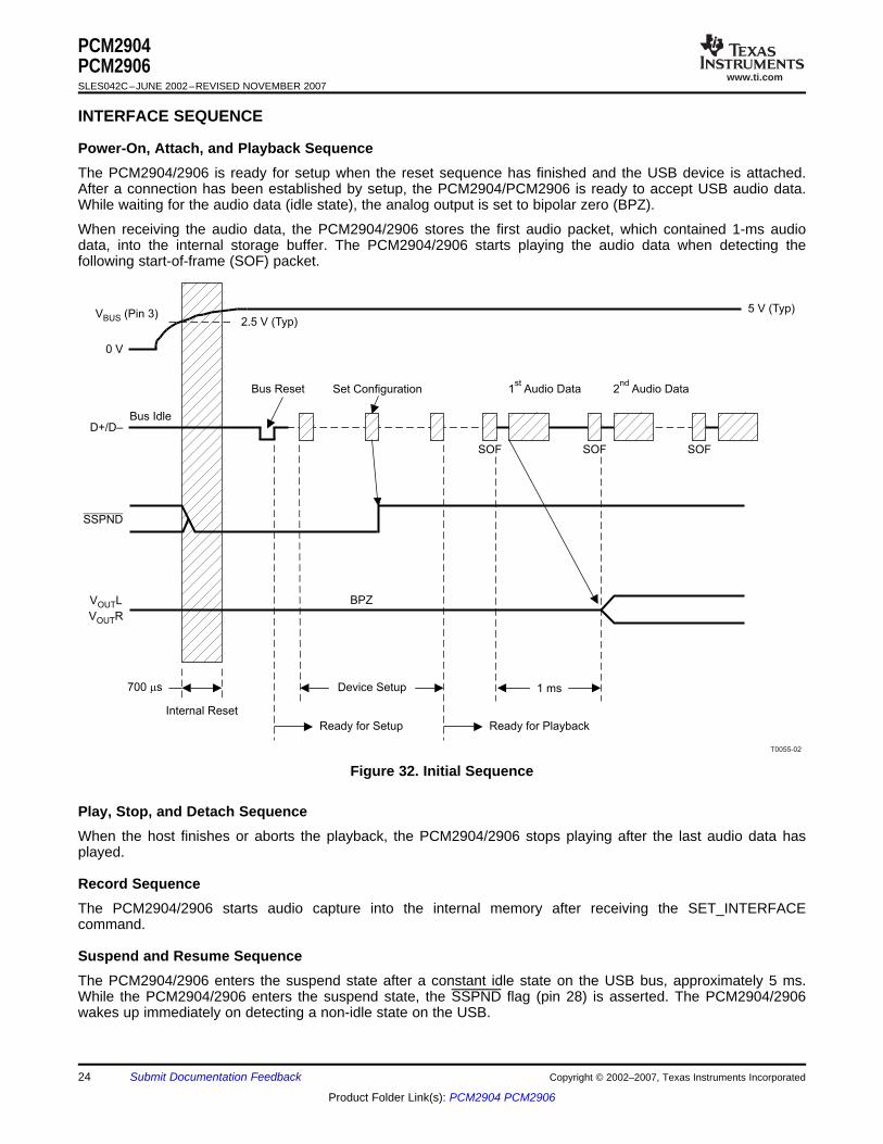
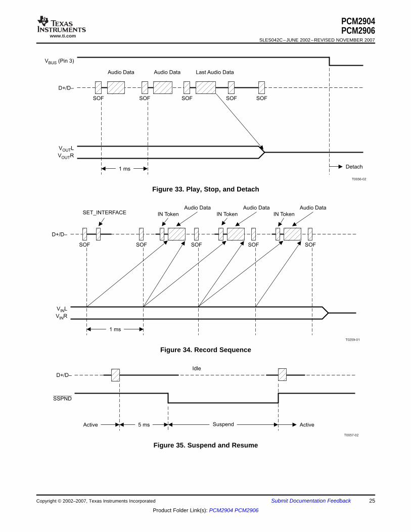
Power-On, Attach, and Playback Sequence
D+/D–
2.5 V (Typ)
0 V
Internal Reset
Ready for Setup
SOF
Ready for Playback
Bus Reset Set Configuration
SOF SOF
BPZ
Bus Idle
5 V (Typ)
1 Audio Datast
2 Audio Datand
V (Pin 3)BUS
SSPND
V LOUT
V ROUT
700 sm Device Setup 1 ms
T0055-02
Play, Stop, and Detach Sequence
Record Sequence
Suspend and Resume Sequence
PCM2904PCM2906SLES042C–JUNE 2002–REVISED NOVEMBER 2007
The PCM2904/2906 is ready for setup when the reset sequence has finished and the USB device is attached.After a connection has been established by setup, the PCM2904/PCM2906 is ready to accept USB audio data.While waiting for the audio data (idle state), the analog output is set to bipolar zero (BPZ).
When receiving the audio data, the PCM2904/2906 stores the first audio packet, which contained 1-ms audiodata, into the internal storage buffer. The PCM2904/2906 starts playing the audio data when detecting thefollowing start-of-frame (SOF) packet.
Figure 32. Initial Sequence
When the host finishes or aborts the playback, the PCM2904/2906 stops playing after the last audio data hasplayed.
The PCM2904/2906 starts audio capture into the internal memory after receiving the SET_INTERFACEcommand.
The PCM2904/2906 enters the suspend state after a constant idle state on the USB bus, approximately 5 ms.While the PCM2904/2906 enters the suspend state, the SSPND flag (pin 28) is asserted. The PCM2904/2906wakes up immediately on detecting a non-idle state on the USB.
24 Submit Documentation Feedback Copyright © 2002–2007, Texas Instruments Incorporated
Product Folder Link(s): PCM2904 PCM2906
www.ti.com
D+/D–
V LOUT
V ROUT
Audio DataAudio Data Last Audio Data
Detach
SOF SOF SOF SOF SOF
1 ms
V (Pin 3)BUS
T0056-02
D+/D–
V LIN
V RIN
1 ms
SET_INTERFACEAudio Data
IN Token
Audio Data
IN Token
Audio Data
IN Token
SOF SOF SOF SOF SOF
T0259-01
5 ms
D+/D–
SSPND
Idle
Active ActiveSuspend
T0057-02
PCM2904PCM2906
SLES042C–JUNE 2002–REVISED NOVEMBER 2007
Figure 33. Play, Stop, and Detach
Figure 34. Record Sequence
Figure 35. Suspend and Resume
Copyright © 2002–2007, Texas Instruments Incorporated Submit Documentation Feedback 25
Product Folder Link(s): PCM2904 PCM2906
www.ti.com
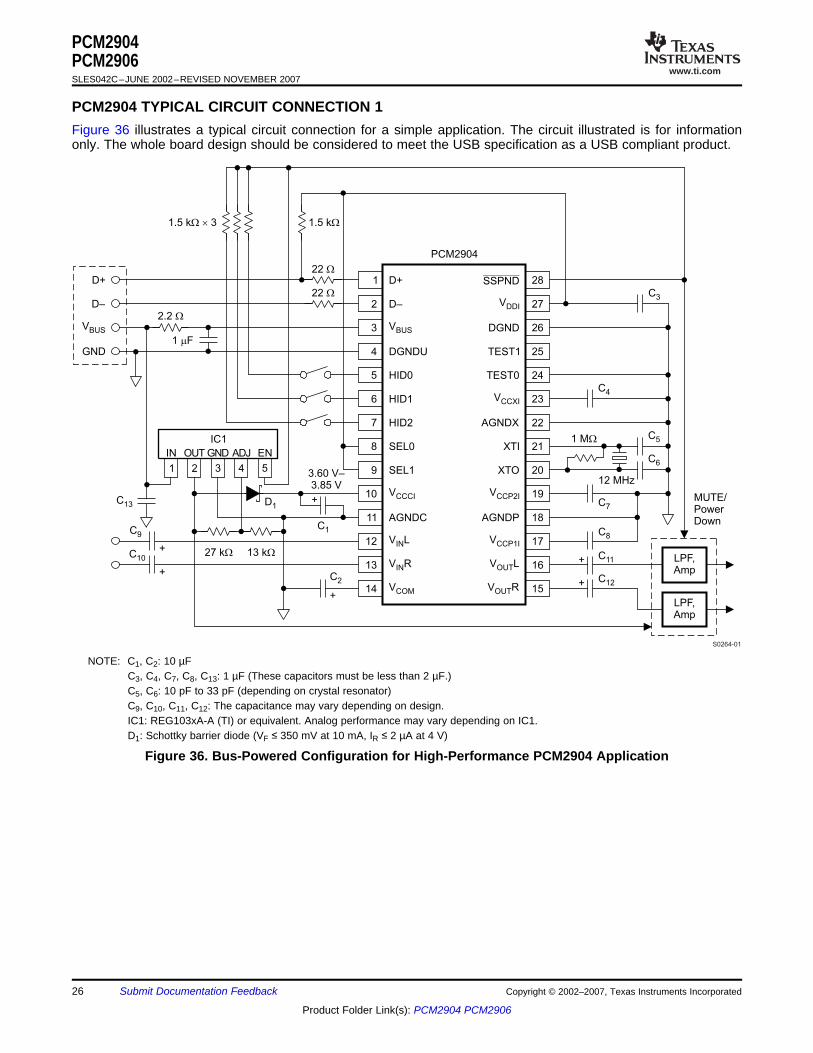
PCM2904 TYPICAL CIRCUIT CONNECTION 1
D+ 28
27
26
25
24
23
22
21
20
19
1
2
3
4
5
6
7
8
9
10
PCM2904
D–
VBUS
DGNDU
HID0
HID1
HID2
SEL0
SEL1
VCCCI
SSPND
XTI
VDDI
DGND
TEST1
TEST0
XTO
VCCP2I
AGNDX
VCCXI
D+
D–
C1
11
12
13
14
AGNDC
V LIN
V RIN
VCOM
18
17
16
15
VCCP1I
V LOUT
V ROUT
AGNDP
22 W
22 W
1.5 k 3W ´ 1.5 kW
GND
VBUS
C2
C9
C10
1 MW
12 MHz
C5
C6
C3
C8
C11
C12
LPF,Amp
LPF,Amp
C7
C4
3.60 V–3.85 V
13 kW27 kW
IN
1
OUT
2
GND
3
ADJ
4
EN
5
IC1
MUTE/PowerDown
+
+
C13
+
+
+
+
D1
2.2 W
1 Fm
S0264-01
PCM2904PCM2906SLES042C–JUNE 2002–REVISED NOVEMBER 2007
Figure 36 illustrates a typical circuit connection for a simple application. The circuit illustrated is for informationonly. The whole board design should be considered to meet the USB specification as a USB compliant product.
NOTE: C1, C2: 10 µFC3, C4, C7, C8, C13: 1 µF (These capacitors must be less than 2 µF.)C5, C6: 10 pF to 33 pF (depending on crystal resonator)C9, C10, C11, C12: The capacitance may vary depending on design.IC1: REG103xA-A (TI) or equivalent. Analog performance may vary depending on IC1.D1: Schottky barrier diode (VF ≤ 350 mV at 10 mA, IR ≤ 2 µA at 4 V)
Figure 36. Bus-Powered Configuration for High-Performance PCM2904 Application
26 Submit Documentation Feedback Copyright © 2002–2007, Texas Instruments Incorporated
Product Folder Link(s): PCM2904 PCM2906
www.ti.com
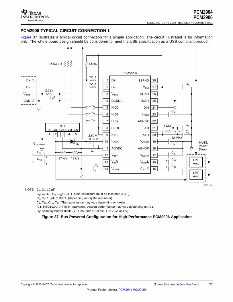
PCM2906 TYPICAL CIRCUIT CONNECTION 1
D+ 28
27
26
25
24
23
22
21
20
19
1
2
3
4
5
6
7
8
9
10
PCM2906
D–
VBUS
DGNDU
HID0
HID1
HID2
SEL0
SEL1
VCCCI
SSPND
XTI
VDDI
DGND
DOUT
DIN
XTO
VCCP2I
AGNDX
VCCXI
D+
D–
C1
11
12
13
14
AGNDC
V LIN
V RIN
VCOM
18
17
16
15
VCCP1I
V LOUT
V ROUT
AGNDP
22 W
22 W
1.5 k 3W ´ 1.5 kW
GND
VBUS
C2
C9
C10
1 MW
12 MHz
C5
C6
C3
C8
C11
C12
LPF,Amp
LPF,Amp
C7
C4
3.60 V–3.85 V
13 kW27 kW
IN
1
OUT
2
GND
3
ADJ
4
EN
5
IC1
MUTE/PowerDown
+
+
C13
+
+
+
+
D1
2.2 W
1 Fm
S0264-02
PCM2904PCM2906
SLES042C–JUNE 2002–REVISED NOVEMBER 2007
Figure 37 illustrates a typical circuit connection for a simple application. The circuit illustrated is for informationonly. The whole board design should be considered to meet the USB specification as a USB compliant product.
NOTE: C1, C2: 10 µFC3, C4, C7, C8, C13: 1 µF (These capacitors must be less than 2 µF.)C5, C6: 10 pF to 33 pF (depending on crystal resonator)C9, C10, C11, C12: The capacitance may vary depending on design.IC1: REG103xA-A (TI) or equivalent. Analog performance may vary depending on IC1.D1: Schottky barrier diode (VF ≤ 350 mV at 10 mA, IR ≤ 2 µA at 4 V)
Figure 37. Bus-Powered Configuration for High-Performance PCM2906 Application
Copyright © 2002–2007, Texas Instruments Incorporated Submit Documentation Feedback 27
Product Folder Link(s): PCM2904 PCM2906
www.ti.com
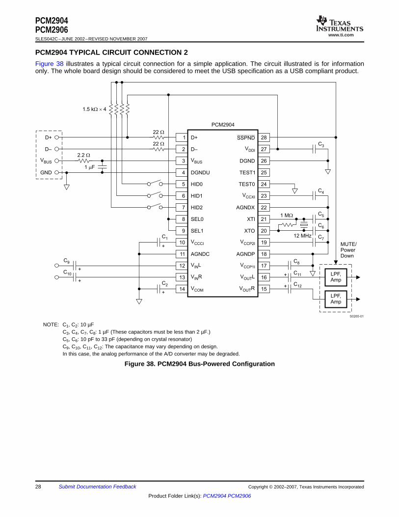
PCM2904 TYPICAL CIRCUIT CONNECTION 2
D+ 28
27
26
25
24
23
22
21
20
19
1
2
3
4
5
6
7
8
9
10
PCM2904
D–
VBUS
DGNDU
HID0
HID1
HID2
SEL0
SEL1
VCCCI
SSPND
XTI
VDDI
DGND
TEST1
TEST0
XTO
VCCP2I
AGNDX
VCCXI
D+
D–
C1
11
12
13
14
AGNDC
V LIN
V RIN
VCOM
18
17
16
15
VCCP1I
V LOUT
V ROUT
AGNDP
22 W
22 W
1.5 k 4W ´
GND
VBUS
C2
C9
C10
1 MW
12 MHz
C5
C6
C3
C8
C11
C12
LPF,Amp
LPF,Amp
C7
C4
MUTE/PowerDown
+
+
+
+
+
+
2.2 W
1 Fm
S0265-01
PCM2904PCM2906SLES042C–JUNE 2002–REVISED NOVEMBER 2007
Figure 38 illustrates a typical circuit connection for a simple application. The circuit illustrated is for informationonly. The whole board design should be considered to meet the USB specification as a USB compliant product.
NOTE: C1, C2: 10 µFC3, C4, C7, C8: 1 µF (These capacitors must be less than 2 µF.)C5, C6: 10 pF to 33 pF (depending on crystal resonator)C9, C10, C11, C12: The capacitance may vary depending on design.In this case, the analog performance of the A/D converter may be degraded.
Figure 38. PCM2904 Bus-Powered Configuration
28 Submit Documentation Feedback Copyright © 2002–2007, Texas Instruments Incorporated
Product Folder Link(s): PCM2904 PCM2906
www.ti.com
PCM2906 TYPICAL CIRCUIT CONNECTION 2
D+ 28
27
26
25
24
23
22
21
20
19
1
2
3
4
5
6
7
8
9
10
PCM2906
D–
VBUS
DGNDU
HID0
HID1
HID2
SEL0
SEL1
VCCCI
SSPND
XTI
VDDI
DGND
DOUT
DIN
XTO
VCCP2I
AGNDX
VCCXI
D+
D–
C1
11
12
13
14
AGNDC
V LIN
V RIN
VCOM
18
17
16
15
VCCP1I
V LOUT
V ROUT
AGNDP
22 W
22 W
1.5 k 4W ´
GND
VBUS
C2
C9
C10
1 MW
12 MHz
C5
C6
C3
C8
C11
C12
LPF,Amp
LPF,Amp
C7
C4
MUTE/PowerDown
+
+
+
+
+
+
2.2 W
1 Fm
S0265-02
PCM2904PCM2906
SLES042C–JUNE 2002–REVISED NOVEMBER 2007
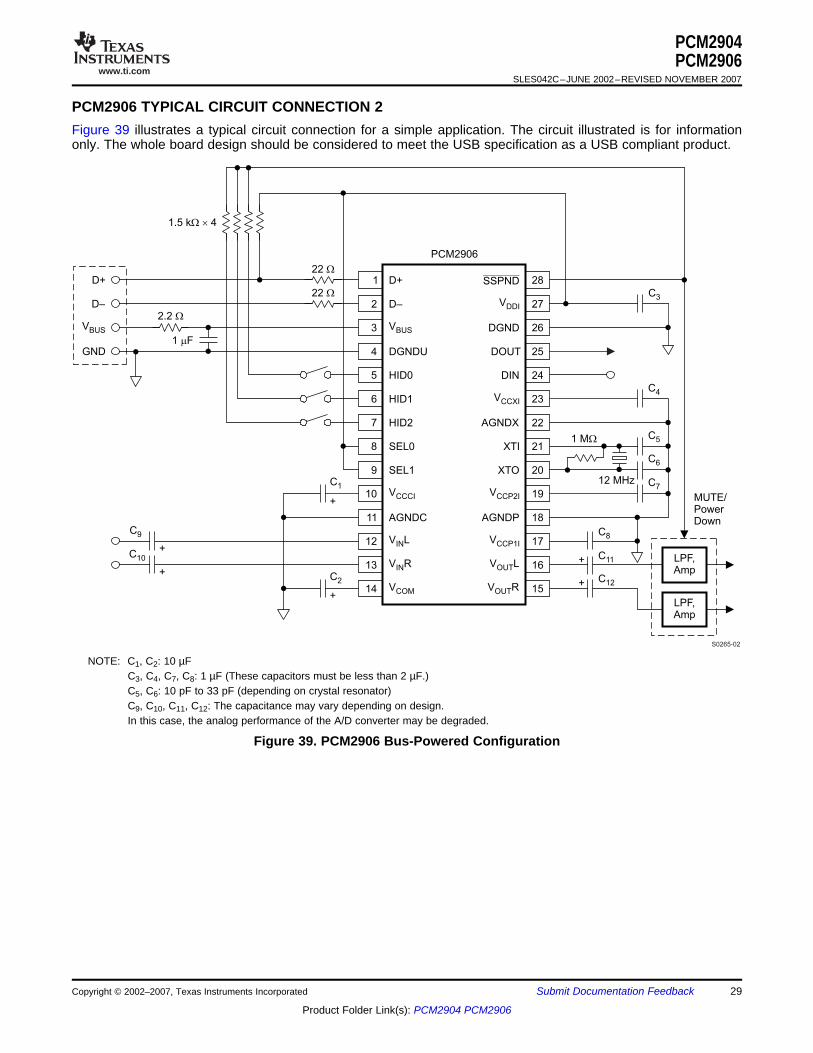
Figure 39 illustrates a typical circuit connection for a simple application. The circuit illustrated is for informationonly. The whole board design should be considered to meet the USB specification as a USB compliant product.
NOTE: C1, C2: 10 µFC3, C4, C7, C8: 1 µF (These capacitors must be less than 2 µF.)C5, C6: 10 pF to 33 pF (depending on crystal resonator)C9, C10, C11, C12: The capacitance may vary depending on design.In this case, the analog performance of the A/D converter may be degraded.
Figure 39. PCM2906 Bus-Powered Configuration
Copyright © 2002–2007, Texas Instruments Incorporated Submit Documentation Feedback 29
Product Folder Link(s): PCM2904 PCM2906
www.ti.com
APPLICATION INFORMATION
OPERATING ENVIRONMENT
PCM2904PCM2906SLES042C–JUNE 2002–REVISED NOVEMBER 2007
For current information on the PCM2904/2906 operating environment, see the Updated Operating Environmentsfor PCM270X, PCM290X Applications application report, SLAA374.
30 Submit Documentation Feedback Copyright © 2002–2007, Texas Instruments Incorporated
Product Folder Link(s): PCM2904 PCM2906
www.ti.com
REVISION HISTORY
PCM2904PCM2906
SLES042C–JUNE 2002–REVISED NOVEMBER 2007
Changes from Revision B (March 2007) to Revision C .................................................................................................. Page
• Deleted operating environment information from data sheet and added reference to application report ........................... 30
Copyright © 2002–2007, Texas Instruments Incorporated Submit Documentation Feedback 31
Product Folder Link(s): PCM2904 PCM2906

MECHANICAL DATA
MSSO002E – JANUARY 1995 – REVISED DECEMBER 2001
POST OFFICE BOX 655303 • DALLAS, TEXAS 75265
DB (R-PDSO-G**) PLASTIC SMALL-OUTLINE
4040065 /E 12/01
28 PINS SHOWN
Gage Plane
8,207,40
0,550,95
0,25
38
12,90
12,30
28
10,50
24
8,50
Seating Plane
9,907,90
30
10,50
9,90
0,38
5,605,00
15
0,22
14
A
28
1
2016
6,506,50
14
0,05 MIN
5,905,90
DIM
A MAX
A MIN
PINS **
2,00 MAX
6,90
7,50
0,65 M0,15
0°–8°
0,10
0,090,25
NOTES: A. All linear dimensions are in millimeters.B. This drawing is subject to change without notice.C. Body dimensions do not include mold flash or protrusion not to exceed 0,15.D. Falls within JEDEC MO-150
IMPORTANT NOTICETexas Instruments Incorporated and its subsidiaries (TI) reserve the right to make corrections, modifications, enhancements, improvements,and other changes to its products and services at any time and to discontinue any product or service without notice. Customers shouldobtain the latest relevant information before placing orders and should verify that such information is current and complete. All products aresold subject to TI’s terms and conditions of sale supplied at the time of order acknowledgment.TI warrants performance of its hardware products to the specifications applicable at the time of sale in accordance with TI’s standardwarranty. Testing and other quality control techniques are used to the extent TI deems necessary to support this warranty. Except wheremandated by government requirements, testing of all parameters of each product is not necessarily performed.TI assumes no liability for applications assistance or customer product design. Customers are responsible for their products andapplications using TI components. To minimize the risks associated with customer products and applications, customers should provideadequate design and operating safeguards.TI does not warrant or represent that any license, either express or implied, is granted under any TI patent right, copyright, mask work right,or other TI intellectual property right relating to any combination, machine, or process in which TI products or services are used. Informationpublished by TI regarding third-party products or services does not constitute a license from TI to use such products or services or awarranty or endorsement thereof. Use of such information may require a license from a third party under the patents or other intellectualproperty of the third party, or a license from TI under the patents or other intellectual property of TI.Reproduction of TI information in TI data books or data sheets is permissible only if reproduction is without alteration and is accompaniedby all associated warranties, conditions, limitations, and notices. Reproduction of this information with alteration is an unfair and deceptivebusiness practice. TI is not responsible or liable for such altered documentation. Information of third parties may be subject to additionalrestrictions.Resale of TI products or services with statements different from or beyond the parameters stated by TI for that product or service voids allexpress and any implied warranties for the associated TI product or service and is an unfair and deceptive business practice. TI is notresponsible or liable for any such statements.TI products are not authorized for use in safety-critical applications (such as life support) where a failure of the TI product would reasonablybe expected to cause severe personal injury or death, unless officers of the parties have executed an agreement specifically governingsuch use. Buyers represent that they have all necessary expertise in the safety and regulatory ramifications of their applications, andacknowledge and agree that they are solely responsible for all legal, regulatory and safety-related requirements concerning their productsand any use of TI products in such safety-critical applications, notwithstanding any applications-related information or support that may beprovided by TI. Further, Buyers must fully indemnify TI and its representatives against any damages arising out of the use of TI products insuch safety-critical applications.TI products are neither designed nor intended for use in military/aerospace applications or environments unless the TI products arespecifically designated by TI as military-grade or "enhanced plastic." Only products designated by TI as military-grade meet militaryspecifications. Buyers acknowledge and agree that any such use of TI products which TI has not designated as military-grade is solely atthe Buyer's risk, and that they are solely responsible for compliance with all legal and regulatory requirements in connection with such use.TI products are neither designed nor intended for use in automotive applications or environments unless the specific TI products aredesignated by TI as compliant with ISO/TS 16949 requirements. Buyers acknowledge and agree that, if they use any non-designatedproducts in automotive applications, TI will not be responsible for any failure to meet such requirements.Following are URLs where you can obtain information on other Texas Instruments products and application solutions:Products ApplicationsAmplifiers amplifier.ti.com Audio www.ti.com/audioData Converters dataconverter.ti.com Automotive www.ti.com/automotiveDLP® Products www.dlp.com Broadband www.ti.com/broadbandDSP dsp.ti.com Digital Control www.ti.com/digitalcontrolClocks and Timers www.ti.com/clocks Medical www.ti.com/medicalInterface interface.ti.com Military www.ti.com/militaryLogic logic.ti.com Optical Networking www.ti.com/opticalnetworkPower Mgmt power.ti.com Security www.ti.com/securityMicrocontrollers microcontroller.ti.com Telephony www.ti.com/telephonyRFID www.ti-rfid.com Video & Imaging www.ti.com/videoRF/IF and ZigBee® Solutions www.ti.com/lprf Wireless www.ti.com/wireless
Mailing Address: Texas Instruments, Post Office Box 655303, Dallas, Texas 75265Copyright © 2009, Texas Instruments Incorporated


![Untitled-1 []...Klipsch RP- 160M 100 Hz f 10 dB '00 dB 90 dB 70 dB Klipsch 160M Pegel- & Klirrverlauf — dB 90 dB — dB — 100 dB 16 Ohm 8 Ohm 2 Ohm 1 Ohm kHz 40 kHz dB 50 dB 20](https://img.dokumen.tips/doc/110x75/60961ba59437253425333804/untitled-1-klipsch-rp-160m-100-hz-f-10-db-00-db-90-db-70-db-klipsch-160m.jpg)