Embed Size (px)
Citation preview
Workshop Summary Report: Scanning Probe Nanolithography Workshop A workshop sponsored by the Precision Engineering Division, Manufacturing Engineering Laboratory, NIST, under a Research Cooperation Agreement on advanced lithography of functional nanostructures signed in 2001 by the National Microelectronics Center of Spain (CNM), the National Institute of Advanced Industrial Science & Technology (AIST) of Japan, and NIST. held at NIST, Gaithersburg MD 20899 on November 12 – 13, 2002
NISTIR 7040 John A. Dagata National Institute of Standards & Technology Hiroshi Yokoyama National Institute of Advanced Industrial Science & Technology of Japan Francesc Perez-Murano National Microelectronics Center of Spain U.S. DEPARTMENT OF COMMERCE Technology Administration National Institute of Standards & Technology Manufacturing Engineering Laboratory Gaithersburg MD 20899 January 2003

2
3
EXECUTIVE SUMMARY A workshop on Scanning Probe Microscope (SPM)-based Nanolithography was held at NIST Gaithersburg on November 24-25, 2002. The meeting was sponsored by the Precision Engineering Division, Manufacturing Engineering Laboratory, NIST, under a Research Cooperation Agreement on advanced lithography of functional nanostructures signed in 2001 by the National Microelectronics Center of Spain (CNM), the National Institute of Advanced Industrial Science & Technology (AIST) of Japan, and NIST. The workshop program focused on fundamental studies in nanoscience, the kinetics and modeling of SPM oxidation, and applications to nanotechnology, Fundamental studies included discussions of current measurement during SPM oxidation, measurement of charge & density variation in SPM oxides, control & understanding of the meniscus shape, and 3-D multiphysics modeling of electrostatics, transport, and chemical reaction during SPM oxidation. Applications to nanotechnology included the fabrication of nano-electronics, nano-photonics, nano-electromechanical, and microfluidic devices and systems. ACKNOWLEDGMENTS We thank Dennis Swyt and Michael Postek of the Precision Engineering Division of NIST for providing financial support for this workshop, Regenia McCloud of the Precision Engineering Division for expert assistance in coordinating visitors’ travel plans and conference preparations, and Steve Knight and Jack Martinez of the NIST Office of Microelectronic Programs for support of the nanoscale metrology group’s nanofabrication program.

4
5
ABSTRACT
A workshop on Scanning Probe Microscope (SPM)-based Nanolithography was held at NIST Gaithersburg on November 24-25, 2002. The meeting was sponsored by the Precision Engineering Division, Manufacturing Engineering Laboratory, NIST, under a Research Cooperation Agreement on advanced lithography of functional nanostructures signed in 2001 by the National Microelectronics Center of Spain (CNM), the National Institute of Advanced Industrial Science & Technology (AIST) of Japan, and NIST. A dozen active collaborators of NIST, AIST, and CNM projects in this emerging field presented their most recent results on fundamental aspects of nanostructure fabrication and characterization and on the application of SPM nanostructures to nano-electronics, nano-optics, and nano-mechanical devices.

6

7
TABLE OF CONTENTS
EXECUTIVE SUMMARY 3 ACKNOWLEDGMENTS 3 ABSTRACT 6 WORKSHOP AGENDA 9 EXTENDED ABSTRACTS 15 PARTICIPANTS LIST 83

8

9
WORKSHOP AGENDA

10
11
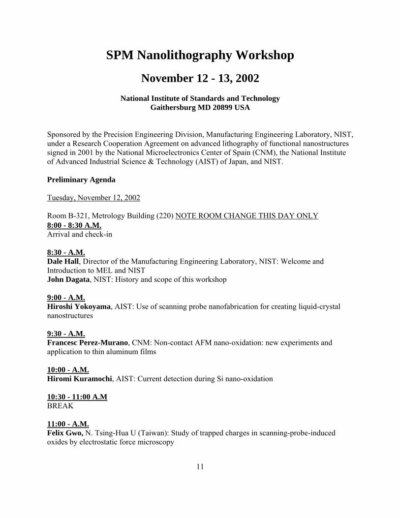
SPM Nanolithography Workshop
November 12 - 13, 2002
National Institute of Standards and Technology Gaithersburg MD 20899 USA
Sponsored by the Precision Engineering Division, Manufacturing Engineering Laboratory, NIST, under a Research Cooperation Agreement on advanced lithography of functional nanostructures signed in 2001 by the National Microelectronics Center of Spain (CNM), the National Institute of Advanced Industrial Science & Technology (AIST) of Japan, and NIST. Preliminary Agenda Tuesday, November 12, 2002 Room B-321, Metrology Building (220) NOTE ROOM CHANGE THIS DAY ONLY 8:00 - 8:30 A.M. Arrival and check-in 8:30 - A.M. Dale Hall, Director of the Manufacturing Engineering Laboratory, NIST: Welcome and Introduction to MEL and NIST John Dagata, NIST: History and scope of this workshop 9:00 - A.M. Hiroshi Yokoyama, AIST: Use of scanning probe nanofabrication for creating liquid-crystal nanostructures 9:30 - A.M. Francesc Perez-Murano, CNM: Non-contact AFM nano-oxidation: new experiments and application to thin aluminum films 10:00 - A.M. Hiromi Kuramochi, AIST: Current detection during Si nano-oxidation 10:30 - 11:00 A.M BREAK 11:00 - A.M. Felix Gwo, N. Tsing-Hua U (Taiwan): Study of trapped charges in scanning-probe-induced oxides by electrostatic force microscopy
12
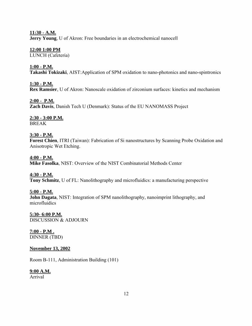
11:30 - A.M. Jerry Young, U of Akron: Free boundaries in an electrochemical nanocell 12:00 1:00 PM LUNCH (Cafeteria) 1:00 - P.M. Takashi Tokizaki, AIST:Application of SPM oxidation to nano-photonics and nano-spintronics 1:30 - P.M. Rex Ramsier, U of Akron: Nanoscale oxidation of zirconium surfaces: kinetics and mechanism 2:00 - P.M. Zach Davis, Danish Tech U (Denmark): Status of the EU NANOMASS Project 2:30 - 3:00 P.M. BREAK 3:30 - P.M. Forest Chien, ITRI (Taiwan): Fabrication of Si nanostructures by Scanning Probe Oxidation and Anisotropic Wet Etching. 4:00 - P.M. Mike Fasolka, NIST: Overview of the NIST Combinatorial Methods Center 4:30 - P.M. Tony Schmitz, U of FL: Nanolithography and microfluidics: a manufacturing perspective 5:00 - P.M. John Dagata, NIST: Integration of SPM nanolithography, nanoimprint lithography, and microfluidics 5:30- 6:00 P.M.DISCUSSION & ADJOURN 7:00 - P.M . DINNER (TBD) November 13, 2002 Room B-111, Administration Building (101) 9:00 A.M. Arrival

13
9:15 - 10:30 A.M. Discussion 1 Topic: Identifying and measuring experimental input parameters required for quantitative modeling of transport and reaction processes during SPM oxidation Francesc Perez-Murano & Jerry Young, discussion leaders 10:30 - 11:00 A.M. BREAK 11:00 A.M. 12:00 P.M. Discussion 2 Topic: Prospects for using SPM oxidation as a materials characterization technique Felix Gwo & Rex Ramsier, discussion leaders 12:00 - 1:00 P.M. LUNCH (Cafeteria) 1:00 - 2:15 P.M. Discussion 3 Topic: Nanostructured templates and self-organized chemistry Hiroshi Yokoyama & Mike Fasolka, discussion leaders 2:15 - 3:15 P.M. BREAK 3:15 - 4:30 Discussion 4 Topic: Designs and timelines for nanofluidic, photonic, and NEMS devices Zach Davis & Forest Chien, discussion leaders 4:30 P.M . ADJOURN

14

15
EXTENDED ABSTRACTS

16
17
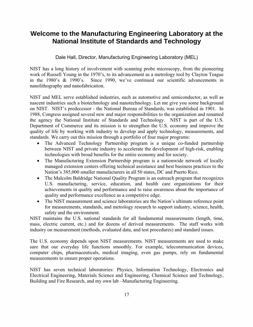
Welcome to the Manufacturing Engineering Laboratory at the National Institute of Standards and Technology
Dale Hall, Director, Manufacturing Engineering Laboratory (MEL) NIST has a long history of involvement with scanning probe microscopy, from the pioneering work of Russell Young in the 1970’s, to its advancement as a metrology tool by Clayton Teague in the 1980’s & 1990’s. Since 1990, we’ve continued our scientific advancements in nanolithography and nanofabrication. NIST and MEL serve established industries, such as automotive and semiconductor, as well as nascent industries such a biotechnology and nanotechnology. Let me give you some background on NIST. NIST’s predecessor - the National Bureau of Standards, was established in 1901. In 1988, Congress assigned several new and major responsibilities to the organization and renamed the agency the National Institute of Standards and Technology. NIST is part of the U.S. Department of Commerce and its mission is to strengthen the U.S. economy and improve the quality of life by working with industry to develop and apply technology, measurements, and standards. We carry out this mission through a portfolio of four major programs:
• The Advanced Technology Partnership program is a unique co-funded partnership between NIST and private industry to accelerate the development of high-risk, enabling technologies with broad benefits for the entire economy and for society.
• The Manufacturing Extension Partnership program is a nationwide network of locally managed extension centers offering technical assistance and best business practices to the Nation’s 385,000 smaller manufacturers in all 50 states, DC and Puerto Rico.
• The Malcolm Baldridge National Quality Program is an outreach program that recognizes U.S. manufacturing, service, education, and health care organizations for their achievements in quality and performance and to raise awareness about the importance of quality and performance excellence as a competitive edge.
• The NIST measurement and science laboratories are the Nation’s ultimate reference point for measurements, standards, and metrology research to support industry, science, health, safety and the environment.
NIST maintains the U.S. national standards for all fundamental measurements (length, time, mass, electric current, etc.) and for dozens of derived measurements. The staff works with industry on measurement (methods, evaluated data, and test procedures) and standard issues. The U.S. economy depends upon NIST measurements. NIST measurements are used to make sure that our everyday life functions smoothly. For example, telecommunication devices, computer chips, pharmaceuticals, medical imaging, even gas pumps, rely on fundamental measurements to ensure proper operations. NIST has seven technical laboratories: Physics, Information Technology, Electronics and Electrical Engineering, Materials Science and Engineering, Chemical Science and Technology, Building and Fire Research, and my own lab –Manufacturing Engineering.
18
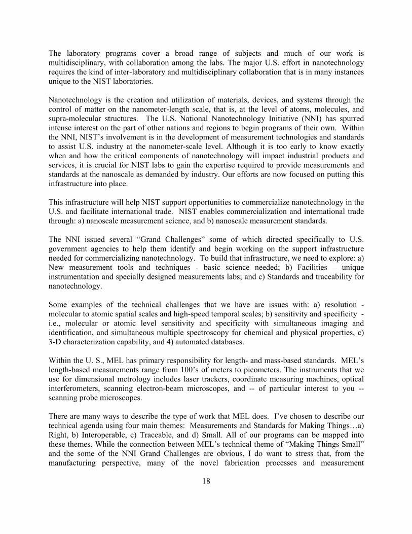
The laboratory programs cover a broad range of subjects and much of our work is multidisciplinary, with collaboration among the labs. The major U.S. effort in nanotechnology requires the kind of inter-laboratory and multidisciplinary collaboration that is in many instances unique to the NIST laboratories. Nanotechnology is the creation and utilization of materials, devices, and systems through the control of matter on the nanometer-length scale, that is, at the level of atoms, molecules, and supra-molecular structures. The U.S. National Nanotechnology Initiative (NNI) has spurred intense interest on the part of other nations and regions to begin programs of their own. Within the NNI, NIST’s involvement is in the development of measurement technologies and standards to assist U.S. industry at the nanometer-scale level. Although it is too early to know exactly when and how the critical components of nanotechnology will impact industrial products and services, it is crucial for NIST labs to gain the expertise required to provide measurements and standards at the nanoscale as demanded by industry. Our efforts are now focused on putting this infrastructure into place. This infrastructure will help NIST support opportunities to commercialize nanotechnology in the U.S. and facilitate international trade. NIST enables commercialization and international trade through: a) nanoscale measurement science, and b) nanoscale measurement standards. The NNI issued several “Grand Challenges” some of which directed specifically to U.S. government agencies to help them identify and begin working on the support infrastructure needed for commercializing nanotechnology. To build that infrastructure, we need to explore: a) New measurement tools and techniques - basic science needed; b) Facilities – unique instrumentation and specially designed measurements labs; and c) Standards and traceability for nanotechnology. Some examples of the technical challenges that we have are issues with: a) resolution - molecular to atomic spatial scales and high-speed temporal scales; b) sensitivity and specificity - i.e., molecular or atomic level sensitivity and specificity with simultaneous imaging and identification, and simultaneous multiple spectroscopy for chemical and physical properties, c) 3-D characterization capability, and 4) automated databases. Within the U. S., MEL has primary responsibility for length- and mass-based standards. MEL’s length-based measurements range from 100’s of meters to picometers. The instruments that we use for dimensional metrology includes laser trackers, coordinate measuring machines, optical interferometers, scanning electron-beam microscopes, and -- of particular interest to you -- scanning probe microscopes. There are many ways to describe the type of work that MEL does. I’ve chosen to describe our technical agenda using four main themes: Measurements and Standards for Making Things…a) Right, b) Interoperable, c) Traceable, and d) Small. All of our programs can be mapped into these themes. While the connection between MEL’s technical theme of “Making Things Small” and the some of the NNI Grand Challenges are obvious, I do want to stress that, from the manufacturing perspective, many of the novel fabrication processes and measurement
19
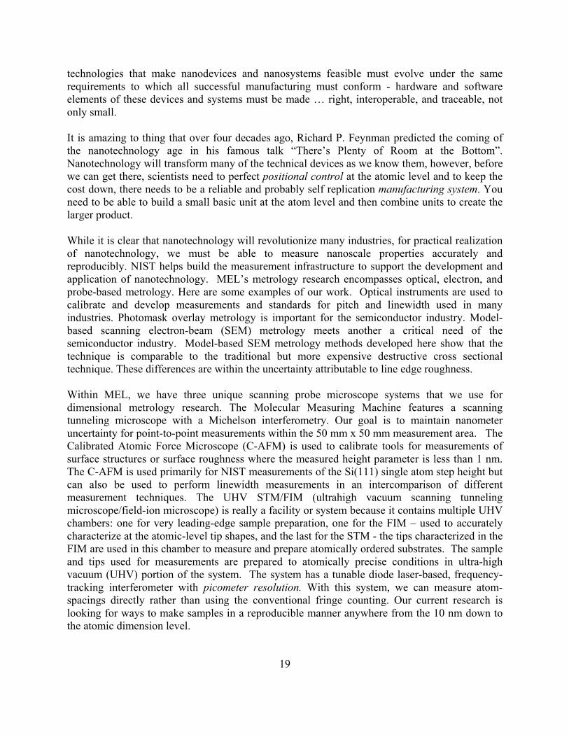
technologies that make nanodevices and nanosystems feasible must evolve under the same requirements to which all successful manufacturing must conform - hardware and software elements of these devices and systems must be made … right, interoperable, and traceable, not only small. It is amazing to thing that over four decades ago, Richard P. Feynman predicted the coming of the nanotechnology age in his famous talk “There’s Plenty of Room at the Bottom”. Nanotechnology will transform many of the technical devices as we know them, however, before we can get there, scientists need to perfect positional control at the atomic level and to keep the cost down, there needs to be a reliable and probably self replication manufacturing system. You need to be able to build a small basic unit at the atom level and then combine units to create the larger product. While it is clear that nanotechnology will revolutionize many industries, for practical realization of nanotechnology, we must be able to measure nanoscale properties accurately and reproducibly. NIST helps build the measurement infrastructure to support the development and application of nanotechnology. MEL’s metrology research encompasses optical, electron, and probe-based metrology. Here are some examples of our work. Optical instruments are used to calibrate and develop measurements and standards for pitch and linewidth used in many industries. Photomask overlay metrology is important for the semiconductor industry. Model-based scanning electron-beam (SEM) metrology meets another a critical need of the semiconductor industry. Model-based SEM metrology methods developed here show that the technique is comparable to the traditional but more expensive destructive cross sectional technique. These differences are within the uncertainty attributable to line edge roughness. Within MEL, we have three unique scanning probe microscope systems that we use for dimensional metrology research. The Molecular Measuring Machine features a scanning tunneling microscope with a Michelson interferometry. Our goal is to maintain nanometer uncertainty for point-to-point measurements within the 50 mm x 50 mm measurement area. The Calibrated Atomic Force Microscope (C-AFM) is used to calibrate tools for measurements of surface structures or surface roughness where the measured height parameter is less than 1 nm. The C-AFM is used primarily for NIST measurements of the Si(111) single atom step height but can also be used to perform linewidth measurements in an intercomparison of different measurement techniques. The UHV STM/FIM (ultrahigh vacuum scanning tunneling microscope/field-ion microscope) is really a facility or system because it contains multiple UHV chambers: one for very leading-edge sample preparation, one for the FIM – used to accurately characterize at the atomic-level tip shapes, and the last for the STM - the tips characterized in the FIM are used in this chamber to measure and prepare atomically ordered substrates. The sample and tips used for measurements are prepared to atomically precise conditions in ultra-high vacuum (UHV) portion of the system. The system has a tunable diode laser-based, frequency-tracking interferometer with picometer resolution. With this system, we can measure atom-spacings directly rather than using the conventional fringe counting. Our current research is looking for ways to make samples in a reproducible manner anywhere from the 10 nm down to the atomic dimension level.
20
MEL is also exploring novel fabrication methods for nanostructures. Let me give you some examples of our own efforts to prototype nanoscale standards. The first example is a pitch calibration prototype designed and prepared here at NIST by scanning probe lithography and silicon etching. These prototypes demonstrate that 100-nm minimum pitch and sub-50-nm linewidth can be obtained. Pitch placement accuracy has been analyzed using statistical methods developed in the optical and SEM dimensional metrology projects. This work was performed in collaboration with a guest researcher from the Center for Measurement Standards in Taiwan, Forest Chien. Another example is a replica of a magnification artifact produced by the 'soft lithography' technique (casting a silicon mold using poly dimethyl siloxane, or PDMS). Since one of the manufacturing goals of nanotechnology is low unit-cost production, there is a great need for, and growing interest in, commercializing rapid and cheap prototyping methods. NIST partners with industrial consortia, individual companies, other government agencies, and universities. When NIST works on a technical issue with its partners, we tend to focus on issues that can benefit industry sectors in a broad sense. Our partnerships typically relate to measurements and standards issues. I would like to encourage further interactions among all of the workshop participants. Successfully bringing nanotechnology to industry will depend on meeting challenges in measurement, fundamental understanding, and control of dimensional and materials properties and processes that work at the nanometer level. Length, height, force, tribology, finish, and composition are just a few of the properties that we must deal with simultaneously in order that components of nanoscale devices and systems are made “right, interoperable, traceable, as well as small.” I encourage you to ask questions and follow up on any of our work that you find interesting. Descriptions of NIST’s or MEL’s technical programs can be found on website – www.nist.gov.
SPM Nanolithography Workshop National Institute of Standards and Technology November 12-13, 2002
History and scope of this workshop
John A. Dagata
Precision Engineering Division Manufacturing Engineering Laboratory
National Institute of Standards and Technology Gaithersburg MD 20899 USA
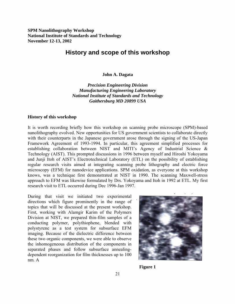
History of this workshop It is worth recording briefly how this workshop on scanning probe microscope (SPM)-based nanolithography evolved. New opportunities for US government scientists to collaborate directly with their counterparts in the Japanese government arose through the signing of the US-Japan Framework Agreement of 1993-1994. In particular, this agreement simplified processes for establishing collaboration between NIST and MITI’s Agency of Industrial Science & Technology (AIST). This prompted discussions in 1996 between myself and Hiroshi Yokoyama and Junji Itoh of AIST’s Electrotechnical Laboratory (ETL) on the possibility of establishing regular research visits aimed at integrating scanning probe lithography and electric force microscopy (EFM) for nanodevice applications. SPM oxidation, as everyone at this workshop knows, was a technique first demonstrated at NIST in 1990. The scanning Maxwell-stress approach to EFM was likewise formulated by Drs. Yokoyama and Itoh in 1992 at ETL. My first research visit to ETL occurred during Dec 1996-Jan 1997. During that visit we initiated two experimental directions which figure prominently in the range of topics that will be discussed at the present workshop. First, working with Alamgir Karim of the Polymers Division at NIST, we prepared thin-film samples of a conducting polymer, polythiophene, blended with polystyrene as a test system for subsurface EFM imaging. Because of the dielectric difference between these two organic components, we were able to observe the inhomogeneous distribution of the components in separated phases and follow subsurface annealing-dependent reorganization for film thicknesses up to 100 nm. A
Figure 1 21
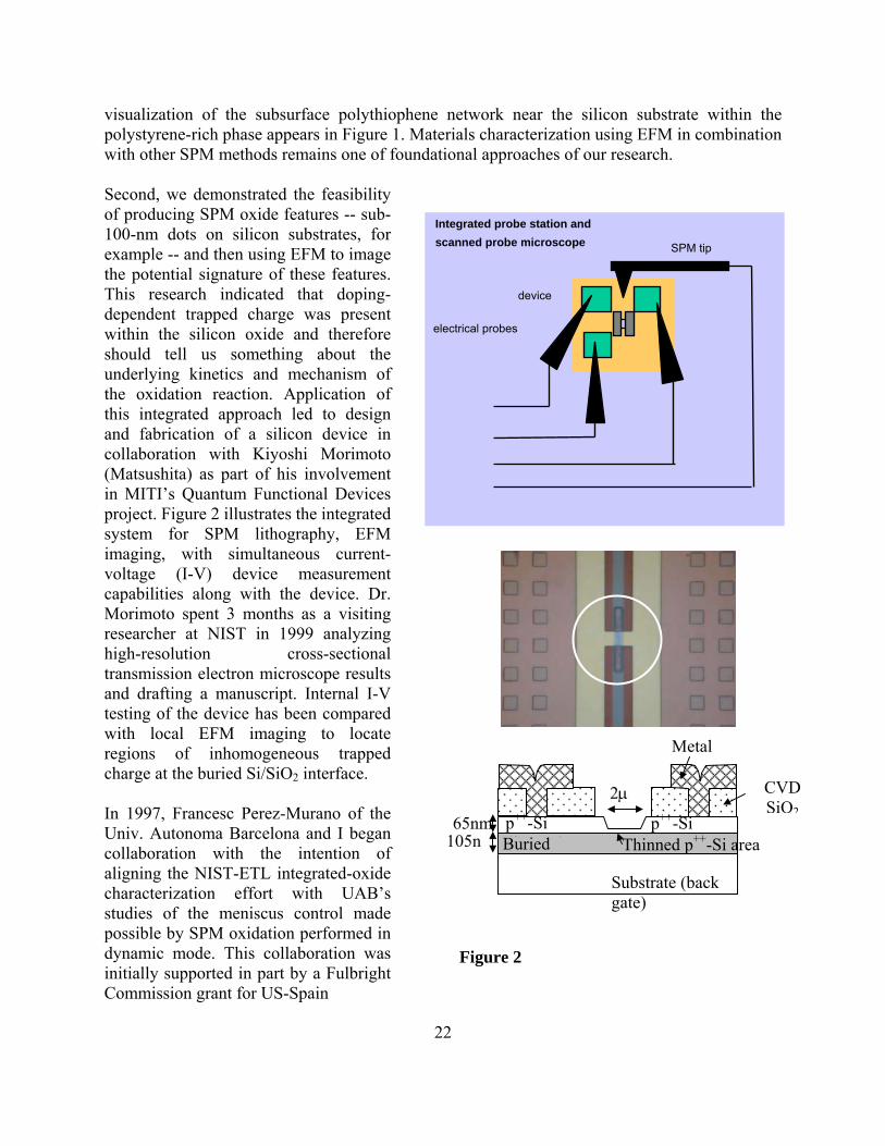
visualization of the subsurface polythiophene network near the silicon substrate within the polystyrene-rich phase appears in Figure 1. Materials characterization using EFM in combination with other SPM methods remains one of foundational approaches of our research. Second, we demonstrated the feasibility of producing SPM oxide features -- sub-100-nm dots on silicon substrates, for example -- and then using EFM to image the potential signature of these features. This research indicated that doping-dependent trapped charge was present within the silicon oxide and therefore should tell us something about the underlying kinetics and mechanism of the oxidation reaction. Application of this integrated approach led to design and fabrication of a silicon device in collaboration with Kiyoshi Morimoto (Matsushita) as part of his involvement in MITI’s Quantum Functional Devices project. Figure 2 illustrates the integrated system for SPM lithography, EFM imaging, with simultaneous current-voltage (I-V) device measurement capabilities along with the device. Dr. Morimoto spent 3 months as a visiting researcher at NIST in 1999 analyzing high-resolution cross-sectional transmission electron microscope results and drafting a manuscript. Internal I-V testing of the device has been compared with local EFM imaging to locate regions of inhomogeneous trapped charge at the buried Si/SiO2 interface.
device
electrical probes
SPM tip
Integrated probe station andscanned probe microscope
Figure 2
105n Buried
Substrate (back gate)
65nm
2μ
Thinned p++-Si area
Metal
CVD SiO2
p++-Si p++-Si (S )
In 1997, Francesc Perez-Murano of the Univ. Autonoma Barcelona and I began collaboration with the intention of aligning the NIST-ETL integrated-oxide characterization effort with UAB’s studies of the meniscus control made possible by SPM oxidation performed in dynamic mode. This collaboration was initially supported in part by a Fulbright Commission grant for US-Spain
22
23
Cooperative Research. Publication of voltage modulation, density variation, and space-charge modeling studies of SPM oxidation were an outcome of this collaboration. After having met in Japan, Europe, and the US at various meetings and workshops1, it became apparent to Hiroshi, Francesc, and I that a more formal agreement would facilitate regular exchange of information, help each of us to focus on new directions, and help to broaden our productive and ongoing discussions to include a wider circle of collaborators. In September 2001 a Cooperative Research Agreement was signed by CNM of Spain, AIST of Japan, and NIST to promote advanced lithography of nanostructures and we agreed to hold this next workshop at NIST. Scope of this workshop The organization of this workshop follows a somewhat arbitrary distinction between fundamental studies in nanoscience – the kinetics and modeling of SPM oxidation -- and applications to nanotechnology, particularly fabrication of nano-electronics, nano-photonics, and nano-electromechanical devices and systems. Fundamental studies that promise to lead to a more complete understanding, predication, and application of SPM oxidation are covered in the following talks:
• Current measurement during SPM oxidation (Francesc Perez-Murano, Hiromi Kuramochi)
• Measurement of charge & density variation in SPM oxides (Felix Gwo)
• Control & understanding of the meniscus shape (Francesc Perez-Murano)
• 3-D multiphysics modeling of electrostatics, transport, and chemical reactions (Jerry
Young). Hiroshi has long argued that reliable current measurements during SPM oxidation are required to complement our earlier EFM measurements of the resulting oxide charge and volume to gain complete understanding and control of the process. The measurements that Francesc and Hiromi Kuramochi (AIST) have made recently are extremely promising in this regard. These efforts represent essential input into the modeling efforts of Jerry Young and his colleagues at the Univ. of Akron in bringing a self-consistent method to solving the system of reaction-diffusion equations. These equations describe the chemical aspects of oxide film growth with the physical description of the electrostatic field that exists within the water meniscus and its dielectric/ionic character during exposure. The extent to which it is becoming possible to control the meniscus shape, and thereby the total current passing through the system, as Francesc discusses in his presentation, must be accounted for within the model. The composition of the resulting oxide
1 SP-Nano I - Tsukuba 1997, QFD Society Meeting - Gaithersburg 1997, SP-Nano II - Tsukuba 1999, Informal workshop on SPM lithography - Tsukuba 2000, Limits to miniaturization - Barcelona 2002, SPM Nanolithography workshop - Gaithersburg 2002.
24
film must reflect the fact that considerable charge may be present within SPM oxide, a result first pointed out in the initial experiments that Hiroshi and I performed in 1996-7. In addition, a satisfactory model must account for the lower density of the oxide and its variability with exposure conditions, as discussed in the papers that Francesc, Dr. Morimoto, and I co-authored in recent years. Since then, Felix Gwo and his group at National Tsing-hua Univ. have adopted a strategy of using in-situ EFM to gain detailed understanding of charge trapping within silicon and silicon nitride films. Using a low-vacuum system for environment and temperature control, they have performed systematic identification of electronic and ionic species and lifetimes. Sustained progress will provide essential input and consistency checks on emerging models. Applications to nanotechnology are described in the following talks:
• Materials characterization (Felix Gwo, Rex Ramsier)
• Nanoelectronic devices (Takashi Tokizaki)
• Nanoelectromechanical systems (Zach Davis)
• Optics and photonics (Hiroshi Yokoyama, Forest Chien, Takashi Tokizaki)
• Microfluidic systems (Tony Schmitz, Mike Fasolka) A basic tenet of nanotechnology – at least in my view – is that fabrication and characterization become inextricably intertwined at the nanoscale. Prototyping efforts that provide value-added information about dimensional and materials properties are a unique aspect of SPM methods. Felix extends the use of EFM to characterization of charge deposited within oxide and nitride films for data storage. Similarly, Rex Ramsier and his group are applying SPM oxide growth kinetics to augment their surface science studies of Zr and ZrN thin films. A significant portion of the data for Zr and ZrN thin films was obtained by Natalia Farkas, a graduate student at Univ of Akron, during a 6-week research visit to NIST in 2001. Of particular interest are the rich and complicated chemical reactions between surface and subsurface oxygen, nitrogen, and hydrogen species that they have catalogued using thermal and e-beam activation. Coupled with Felix’s evidence for complete conversion of Si3N4 to SiOx by SPM oxidation, it will be very satisfying to understand the details of the corresponding conversion in the ZrN system. A compelling aspect of SPM oxidation is that almost every material oxidizes under the extreme electric-field conditions that exist between the tip and substrate during SPM oxidation. Examples of SPM oxide patterning of device-related materials that have appeared in the literature recently include diamond, superconducting materials, magnetic, and 2-D electron gas in III-V semiconductors. Spintronic devices are being studied with great interest currently and Takashi Tokizaki (AIST) reports on his efforts to pattern such materials. Zach Davis (Danish Tech. Univ.) provides a status report on fabricating a nanomechanical resonator using SPM oxidation. SPM oxidation is combined with laser lithography of an aluminum film to pattern the mask
25
defining the resonator structure by reactive ion etching. A key aspect of this joint research activity between the Danish Microelectronic Center and the National Microelectronics Center of Spain is that the processing sequence is integrated with standard CMOS technology. This work is being funded under a European Union research grant now in Phase II. Optics and photonics applications of SPM lithography are underway and a number of ideas and directions will be presented. Hiroshi is also the leader of an ERATO project in Japan and in this role discusses the use of SPM lithography for patterning liquid-crystals with elegant control of domains at the sub-micrometer scale. Forest Chien of the Industrial Technology Research Institute of Taiwan discusses fabrication of 2-D silicon nanoarrays using SPM oxidation and anisotropic wet etching for potential use as photonic crystals. Forest spent 6 months as a visiting researcher at NIST extending his PhD-thesis work on KOH etching to tetra-methyl ammonium hydroxide etchants and Si(100) and silicon-on-insulator (SOI) substrates, providing a significant database for the optimum production of sub-micrometer silicon nanostructures. Takashi Tokizaki also reviews his unique work using an Al-coated near-field scanning optical microscope (NSOM) tip to simultaneously perform SPM oxidation of a sub-wavelength optical waveguide and measure the resulting optical transmission characteristics. Finally, Mike Fasolka (NIST) describes the mission and capabilities of the NIST Combinatorial Methods Center. During the past year Mike and I have identified several opportunities for combining dimensional and chemical patterning with the gradient methods being developed by the Center. In his presentation, Tony Schmitz (Univ. of FL) summarizes our collaboration during the past year aimed at gaining basic expertise in microfluidic device fabrication and nanoimprint lithography using hot embossing techniques. Our initial results suggest that microfluidic devices provide a significant platform for incorporating SPM-fabricated nanostructures in the near future.

26
27
Tri-stable nematic liquid-crystal device using orientationally frustrated surface patterns fabricated by the atomic force
microscopy nanorubbing
Hiroshi Yokoyama*†, Jong-Hyun Kim* and Makoto Yoneya*
*Yokoyama Nano-structured Liquid Crystal Project, ERATO, Japan Science and Technology Corporation, TRC 5-9-9 Tokodai, Tsukuba, Ibaraki 300-2635, Japan, †Nanotechnology Research Institute, National Institute of Advanced Industrial Science and Technology 1-1-1 Umezono, Tsukuba, Ibaraki 305-8568, Japan
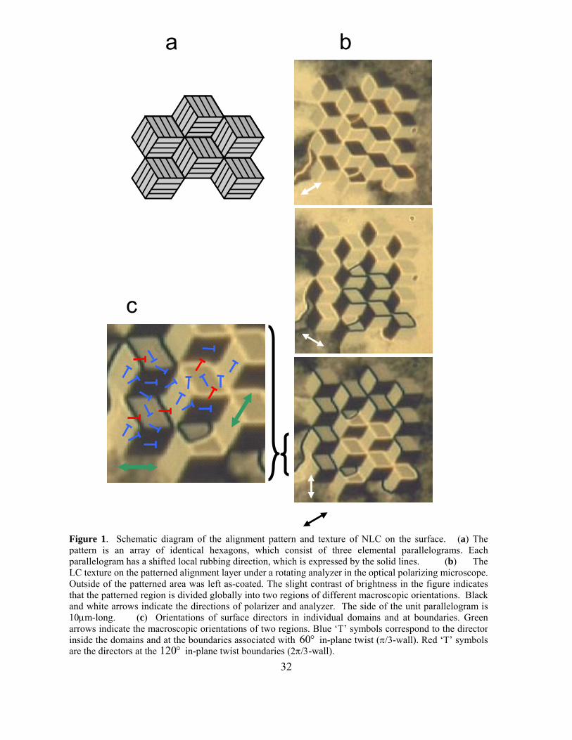
Multi-stable liquid-crystal (LC) devices are known for many years to be desirable for realizing drastically reduced power consumption needed for high information content mobile displays. However, no industrially feasible multi-stable nematic liquid-crystal (NLC) device has ever been realized due to their inherent uniaxial symmetry1-7. Recently we demonstrated a robust surface-alignment bistability on micro-fabricated orientational checkerboard pattern, in which neighbouring unit square domains are so treated as to enforce mutually orthogonal alignment8,9. The four-fold symmetry of the pattern automatically allowed the two diagonal axes of the checkerboard to become equally stable macroscopic orientations. Here we report the first tri-stable surface alignment of NLCs tailored by extending the symmetry approach. A six-fold symmetrical orientational micro pattern was inscribed on polyimide surface by nano-rubbing using the stylus of atomic force microscope (AFM). The surface is tiled with 60-degree rotated nano-rubbed parallelograms. The hexagonal symmetry ensures the three local rubbing directions to give stable macroscopic LC orientations in the bulk, which are mutually switchable by an in-plane electric field. The new LC mode is surface-driven and hence essentially compatible with ever demanding flexible display applications. The present result also illustrates how a nanotechnology tool can be useful in prototyping a cutting edge LC device.
It has long been known that, on a fresh surface of a cleaved single crystal such as NaCl, mica, etc., NLCs can assume multiply stable orientations, faithfully reflecting the crystallographic axes10-12. Given the microscopic uniformity of the cleavage surface, the ordinary anchoring energy coefficient, which is generally represented by a second rank tensor1, should be isotropic for surfaces with four-fold or higher-order symmetries. This implies that the multi-stability observed on single crystal surfaces is a higher-order anchoring effect that makes it susceptible to external contaminants and disturbances leading to the first-order anchoring effect13.
Borrowing the concept of symmetry on single crystals while retaining the first-order robustness of our frustrated micro-patterning, we devised a higher symmetry surface patterns to
realize artificial multi-stability of NLCs. As an example of this approach, we demonstrate here a tri-stability on a hexagonally symmetric pattern consisting of locally rubbed parallelograms as shown in Fig.1. The shape of the parallelogram was designed to have the corner angles of and so that three of them, mutually rotated by
°60°120 °± 60 , make a hexagon. The infinitely
extended pattern tiled with the hexagons (Fig1a) has a six-fold rotational symmetry.
For the purpose of examining the aligning characteristics of the orientational pattern, we fabricated a structure comprised of unit domains as large as 10μm (Fig.1b). We carried out the nano-rubbing on a polyimide-coated glass slide14-17, the details of which have been described elsewhere8,9,17. In brief, the precursory polyamic acid (SE-150, Nissan Chemical Co.) was spun on the glass slide and was baked. For the nano-rubbing, an AFM ( SPA-500, Seiko Instruments Inc.) was used in the contact mode. The nano-rubbed polyimide surface acquired the ability to align LC in parallel to the surface along the symmetrically scanned direction, giving a zero tilt bias angle17. A room temperature NLC, 4-n-pentyl-4’-cyanobiphenyl (5CB), was applied onto the patterned surface to an appropriate thickness without a cover slide.
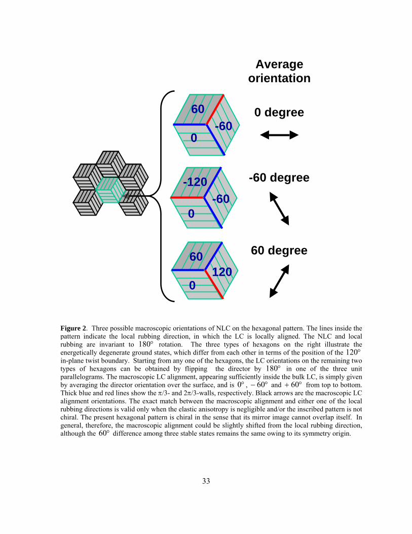
Since the size of the unit domain is large here, LC orientations on individual domains and at the domain boundaries are clearly resolved in the micrographs (Fig1b). The contrast changes under a rotating analyzer confirm that the alignment inside the unit domain is along the local rubbing direction. The domain boundaries also have a distinct brightness, reflecting the alignment transition from one domain to the next. As indicated by the director symbols in Fig1c, two of the three boundaries meeting at a corner are associated with in-plane rotation from one domain to the next (π/3-wall), whereas the remaining one is associated with rotation (2π/3-wall). This combination of walls corresponds to the lowest free-energy configuration that can cover the entire surface without introduction of point defects. Depending on the position of the 2π/3-wall boundary, there appear three orientationally distinct, yet energetically equivalent states as depicted in Fig.2. These states are mutually convertible by way of rotation of the director in an appropriate one of the three constituent parallelograms, and are the basis of the present tri-stability. The global configuration of the director for a given surface orientation is determined in such a way as to minimize orientational distortions described by the Frank elastic energy
°60°120
°180
18. Consequently, the inhomogeneous LC orientation imposed by the patterned surface relaxes rapidly into a uniform bulk alignment, which bears three stable axes depending on the relative arrangement of π/3- and 2π/3-walls. More quantitatively, if we assume the one-constant approximation, the equilibrium configuration of the director azimuth φ satisfies the Laplace equation 180=φΔ . It follows that the laterally inhomogeneous component of φ with the wave vector k decays exponentially as )exp( zk− with the distance along the surface normal into the bulk LC. Therefore, the director profile at a point away from the surface by a distance larger than the unit domain size d becomes virtually uniform with the orientation
z
)0()z =( φφ , where denotes the average over the surface. This shows that one stable bulk orientation is identical
with the local orientation on the unit domain located between the two 3/π -walls. The remaining two stable states are generated from this configuration by the natural symmetry operation of
28
NLCs to flip the surface director by over any particular subset of parallelograms (Fig.2), giving rise to a shift of
°180°60 )0(φ .
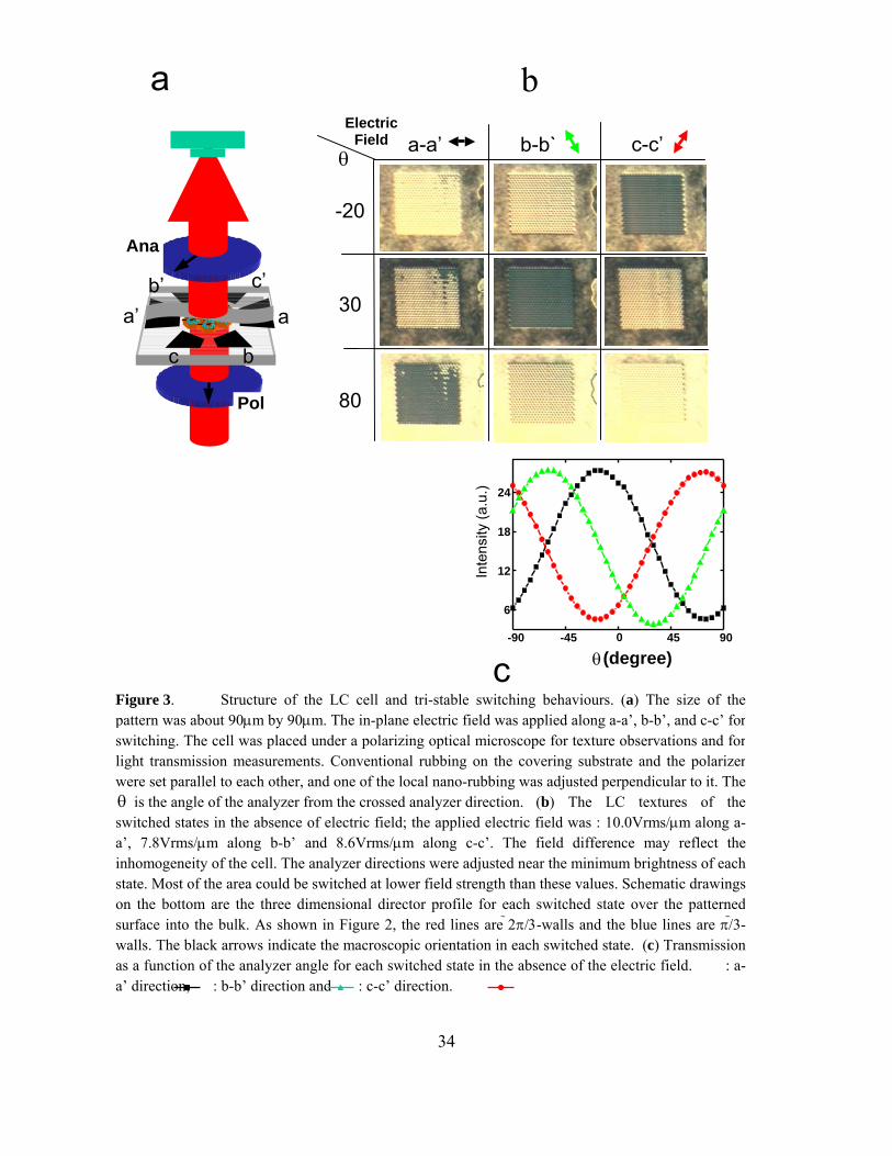
To confirm the tri-stabile alignment, the hexagonal pattern was scaled down to the quarter of the aforementioned pattern to be of 2.4μm side length. As the size of the unit domain approaches the wavelength of visible light, the optical uniformity of the patterned area rapidly improves for the decrease of the orientational relaxation length k/1 and the increase of the optical diffraction angle beyond the numerical aperture of the observation optics. By combining the patterned substrate with a counter polyimide-coated glass slide that was conventionally rubbed, a 50μm –thick sandwich-type LC cell was fabricated (Fig3a). On the glass substrate also fabricated were three pair of electrodes to apply in-plane electric fields, concentrically arranged with shift as shown in Fig3a. The AFM nano-rubbing was conducted in the central space between electrodes. Nano-rubbing directions were set parallel with the electric field directions. The vacant cell was injected with the NLC. Sinusoidal electric field of 1kHz was used for electro-optical switching experiments.
°60
As shown in Figs.3b and 3c, the hexagonally patterned area clearly showed three stable states that were mutually switchable by the electric field. The stable states were found resistant to mechanical disturbances for no-disruption of alignment in prolonged experimentation. This appears reasonable in that the effective anchoring energy of the tri-stable cell is reduced only by 1/3 of a uniform cell, because the switching is associated with the flip of local director on 1/3 of the unit parallelograms. As the field is increased along the destination direction, the LC in bulk starts to reorient along the field. Up to a certain threshold field m/V6 μ≈ , the alignment relaxes back to the original state as the field is turned off. When the field strength exceeds the threshold field, the switching begins locally by the domain nucleation and growth. Due to various inhomogeneities associated with LC injection, non-uniform electric and director field distributions on the pattern boundary, the switching cannot be ideally abrupt, but the field should be a little increased before the entire area is switched. While the three different states switched reversibly between each other, the field strength necessary to drive the a-a’ switching was found to be larger than those for others (b-b’ and c-c’). The difference might reflect the persistent effect of flow alignment during LC injection19, which took place nearly perpendicular to the a-a’. The optical transmission measurements revealed that the contrast ratio was about 5 for all states (Fig3c). This ratio has been improved to ca. 20 for a tri-stable device with 1.2μm unit domain. The angle differences between the stable states were not exactly , but they were about symmetrically about the LC injection direction.
°60 °50
The switching behaviour can be readily analyzed for the extreme cases of small and large unit domains relative to the anchoring extrapolation length 022 ; here, and 0W are the twist elastic constant and anchoring energy, respectively. In the limit of small unit domains
e , the elastic force overwhelms the surface anchoring, thereby making the alignment microscopically uniform
/WKde = 22K
dd <<8. For large unit domains , on the other hand, we can treat the edd >>
29
system as a uniform planar structure subjected to an in-plain field and obtain the threshold field as ΔεK/WCE Mth 220 2= for Rapini-Papoular anchoring1. εΔ is the dielectric anisotropy and
(( ))EeM C φφ −+= 312 tanarctan2cos31 is a symmetry factor depending on the relative azimuthal angle of the field Eφ and the easy direction on the parallelogram eφ . For the tri-stability °=− 60Ee φφ , one obtains 05.1≅MC , which shows that the threshold field remains only 5% higher than that for the bistability. The observed mV/6~ μthE is consistent with this estimate, given mV/5~ μthE and for the bistability2-4
0 J/m10≈W 8. It follows that the angle, ( )|| Ee φφ −± 31tanarctan , by which the surface director should rotate before the switching slightly
increases from (bistability) to (tri-stability). °45 °2.50
As in the ordinary NLC devices, the cell thickness is a critical parameter determining the electro-optic response. Due to the patterned nature of the tri-stable surface, there appears a lower bound for the cell thickness t , set by the condition that the surface inhomogeneity should sufficiently relax inside the cell, i.e.,
dπ2/ddt >> , to give uniform LC alignment to assure
quasi-homogeneous optical and elastic behaviours. Only under this condition, the surface switching can be initiated by the in-plane Freedericksz transition in bulk as required by the switching mechanism8. For a domain size of m1μ≈d , one may safely adopt a thickness
m5μ≈td , indicating that the response speed of the tri-stable device can at least be comparable with that of existing NLC devices. The thickness m50μ≈td used in the present study is obviously an overly safe choice, solely taken for demonstration purposes.
In conclusion, we demonstrated for the first time the orientational tri-stability, which could be switched by an in-plane electric field. The present approach is believed to be generic, based only on the frustration of the periodically aligned LC, not relying on any delicate balance of multi-directional forces, and may be extendable to even higher degree of stabilities. Consequently, the property of the tri-stability is not sensitive to the material or fabrication parameters. The anisotropic LC properties coupled with the symmetry of the substrate will open up a rich new area of electro-optical applications and interfacial sciences of liquid crystals.
References
1. Yokoyama, H. in Handbook of Liquid Crystal Research (ed. Collings, P. J. & Patel, J. S.) Ch. 6 (Oxford Univ. Press, New York, 1997).
2. Boyd, G. D, Cheng, J. & Ngo, P. D. T. Liquid-crystal orientational bistability and nematic storage effects. Appl. Phys. Lett. 36, 556-558 (1980).
3. Berreman, D. W. & Heffner, W. R. New bistable liquid-crystal twist cell. J. Appl. Phys. 52, 3032-3039 (1981).
4. Scheffer, T. J. & Nehring, J. A new, highly multiplexable liquid crystal display. Appl. Phys. Lett. 22, 1021-1023 (1984).
30
31
5. Yang, K. H. Weak boundary storage effect in homogeneous liquid crystal cells. Jpn. J. Appl. Phys. 22, 389-393 (1983).
6. Ong, H., Meyer, R. B. & Hurd, A. J. Multistable orientation in a nematic liquid-crystal cell induced by external-field and interfacial interaction. J. Appl. Phys. 55, 2809-2815 (1984).
7. Barberi, R., Boix, M. & Durand, G. Electrically controlled surface bistability in nematic liquid crystals. Appl. Phys. Lett. 55, 2506-2508 (1989).
8. Kim, J. H., Yoneya, M., Yamamoto, J. & Yokoyama, H. Surface alignment bistability of nematic liquid crystals by orientationally frustrated surface patterns. Appl. Phys. Lett. 78, 3055-3057 (2001).
9. Kim, J. H., Yoneya, M., Yamamoto, J. & Yokoyama, H. Controlling surface alignment on nanoscopically tailored competing domains. Mol. Cryst. Liq. Cryst. 367, 151-158 (2001).
10. Blinov, L. M. & Sonin, A. A. The interaction of nematic liquid crystals with anisotropic substrates. Mol. Cryst. Liq. Cryst. 179, 13-25 (1990).
11. Schuddeboom, P. C. & Jerome, B. Azimuthal anchoring of liquid crystals on surfaces with high symmetry. Phys. Rev. E. 56, 4294-4305 (1997).
12. Schuddeboom, P. C. & Jerome, B. Multistable bulk orientation induced by highly symmetric liquid-crystal monolayer. Europhys. Lett. 39, 515-520 (1997).
13. Yoneya, M., Kim, J. H. & Yokoyama, H. Simple model for patterned bidirectional anchoring of nematic liquid crystal and its bistability. Appl. Phys. Lett. 80, 374-376 (2002).
14. Ruestschim, M., Grutter, P., Funfschilling, J. & Guntherodt, H. J. Creation of liquid crystal waveguides with scanning force microscopy. Science, 265, 512-514 (1994).
15. Pidduck, A. J., Haslam, S. D., Bryan-Brown, G. P., Bannister, R. & Kitely, I. D. Control of liquid crystal alignment by polyimide surface modification using atomic force microscopy. Appl. Phys. Lett. 71, 2907-2909 (1997).
16. Rastegar, A., Skarabot, M., Blij, B. & Rasing, Th. Mechanism of liquid crystal alignment on submicron patterned surfaces. J. Appl. Phys. 89, 960-964 (2001).
17. Kim, J. H., Yoneya, M., Yamamoto, J. & Yokoyama, H. Nano-rubbing of a liquid crystal alignment layer by an atomic force microscope: a detailed characterization. Nanotechnology 13, 133-137 (2002).
18. de Gennes, P. G. & Prost, J. The Physics of Liquid Crystals, (Oxford Univ. Press, New York, 1993).
19. Yamaguchi, R. & Sato, S. Determination of nematic liquid crystal (NLC) orientation by observing NLC droplets on alignment surfaces. Jpn. J. Appl. Phys. 35, L117-L119 (1996).
a b
c
Figure 1. Schematic diagram of the alignment pattern and texture of NLC on the surface. (a) The pattern is an array of identical hexagons, which consist of three elemental parallelograms. Each parallelogram has a shifted local rubbing direction, which is expressed by the solid lines. (b) The LC texture on the patterned alignment layer under a rotating analyzer in the optical polarizing microscope. Outside of the patterned area was left as-coated. The slight contrast of brightness in the figure indicatesthat the patterned region is divided globally into two regions of different macroscopic orientations. Black and white arrows indicate the directions of polarizer and analyzer. The side of the unit parallelogram is 10μm-long. (c) Orientations of surface directors in individual domains and at boundaries. Green arrows indicate the macroscopic orientations of two regions. Blue ‘T’ symbols correspond to the director inside the domains and at the boundaries associated with °60 in-plane twist (π/3-wall). Red ‘T’ symbols are the directors at the °120 in-plane twist boundaries (2π/3-wall). 32
1200
60 60 degree
-600
60 0 degree
-60-120
0
-60 degree
Average orientation
Figure 2. Three possible macroscopic orientations of NLC on the hexagonal pattern. The lines inside thepattern indicate the local rubbing direction, in which the LC is locally aligned. The NLC and localrubbing are invariant to °180 rotation. The three types of hexagons on the right illustrate theenergetically degenerate ground states, which differ from each other in terms of the position of the °120in-plane twist boundary. Starting from any one of the hexagons, the LC orientations on the remaining twotypes of hexagons can be obtained by flipping the director by °180 in one of the three unitparallelograms. The macroscopic LC alignment, appearing sufficiently inside the bulk LC, is simply givenby averaging the director orientation over the surface, and is °0 , °− 60 and °+ 60 from top to bottom.Thick blue and red lines show the π/3- and 2π/3-walls, respectively. Black arrows are the macroscopic LCalignment orientations. The exact match between the macroscopic alignment and either one of the localrubbing directions is valid only when the elastic anisotropy is negligible and/or the inscribed pattern is notchiral. The present hexagonal pattern is chiral in the sense that its mirror image cannot overlap itself. Ingeneral, therefore, the macroscopic alignment could be slightly shifted from the local rubbing direction,although the °60 difference among three stable states remains the same owing to its symmetry origin.
33
c θ-90 -45 0 45 90
6
12
18
24In
tens
ity (a
.u.)
(degree)
ba
a’ a
Pol
bc
-20
30
80
a-a’ b-b` c-c’θ
Electric Field
b’ c’
Ana
Figure 3. Structure of the LC cell and tri-stable switching behaviours. (a) The size of thepattern was about 90μm by 90μm. The in-plane electric field was applied along a-a’, b-b’, and c-c’ forswitching. The cell was placed under a polarizing optical microscope for texture observations and forlight transmission measurements. Conventional rubbing on the covering substrate and the polarizerwere set parallel to each other, and one of the local nano-rubbing was adjusted perpendicular to it. Theθ is the angle of the analyzer from the crossed analyzer direction. (b) The LC textures of theswitched states in the absence of electric field; the applied electric field was : 10.0Vrms/μm along a-a’, 7.8Vrms/μm along b-b’ and 8.6Vrms/μm along c-c’. The field difference may reflect theinhomogeneity of the cell. The analyzer directions were adjusted near the minimum brightness of eachstate. Most of the area could be switched at lower field strength than these values. Schematic drawingson the bottom are the three dimensional director profile for each switched state over the patternedsurface into the bulk. As shown in Figure 2, the red lines are 2π/3-walls and the blue lines are π/ 3-walls. The black arrows indicate the macroscopic orientation in each switched state. (c) Transmissionas a function of the analyzer angle for each switched state in the absence of the electric field. : a-a’ direction, : b-b’ direction and : c-c’ direction.
34
35
Non contact AFM nano-oxidation: Recent experiments and application to thin aluminum layers
Francesc Pérez Murano
Institut de Microelectrònica de Barcelona (IMB-CNM-CSIC)
Abstract
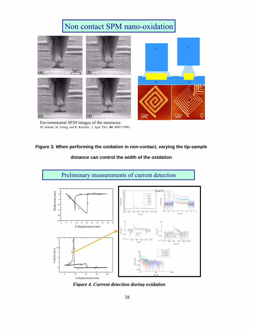
Despite that many examples of nanostructure and device fabrication using SPM nano-oxidation have been reported, a deep study of the oxidation mechanism and kinetics is still missing. In this presentation, I will review some of the most relevant results that have been published for the understanding of the mechanism and kinetics. This information is related with the role of the meniscus when the AFM oxidation is performed at a finite tip-sample distance, and with the electrical current detection during oxidation. Finally, the advantage of using non-contact AFM for nano-oxidation of thin aluminum layers is described 1.- Recent results of AFM nano-oxidation. Figure 1 shows the general concept of the SPM oxidation mechanism on silicon: the oxidation reaction takes place at the silicon/oxide interface; as a product of the reaction H+ is created, which contribute to the creation of defects in the oxide. In addition to this, the water meniscus connecting tip and surface provides the adequate conditions (OH- concentration) for the oxidation to proceed. The most direct evidence of the consequent space charge build-up on the oxide is provided from SMM measurements performed in ref. [1]. Space charge build-up in the oxide is a clue factor for understanding oxidation kinetics. This has been analyzed in reference 2, where a model for the kinetics of oxide growth has been elaborated, which predicts the temporal evolution of defect and intermediate species creation [2]. A way to show up the effect of space charge in the oxide growth kinetics consists on performing the oxidation under AC voltage. Figure 2 shows some examples of how the kinetics is changed under AC voltage, both in height vs. time and width vs. time [3]. An additional consequence of space charge build-up in the oxide is the low density of the SPM oxide compared to thermally grown oxide. After an annealing, the density of the oxide increases as it has been determined from the XTEM analysis [4]. The kinetics of the oxide growth can be also modified by manipulating the water meniscus, i.e., by changing the tip-sample distance when doing the oxidation in non-contact mode. Figure 3 shows the effect of changing the tip sample distance while inducing the oxidation. Environmental SEM images of the meniscus provide a nice representation of the role of the meniscus. The interplay between water meniscus and space charge build-up in the oxide can be further analyzed by detecting the current during the SPM oxidation. Figures 4 and 5 show preliminary measurements of current detection during oxidation (figure 4) and meniscus conductivity. For all the data, stiff cantilevers (k=40 N/m) with n-doped silicon tips have been used. Current acquisition is performed simultaneously to the acquisition of a force vs. distance curve, so that the dependence of current vs. tip-sample distance (as well as the current evolution with time) can be established.
36
2.- AFM nano-oxidation of thin aluminum layers Figure 6 shows AFM images of the aluminum surface used in the experiments. Although surface is very rough compared to the surface of a silicon wafer, it is good enough for serving as a template for AFM oxidation experiments. Al thin films (thickness of 8 nm) have been deposited by sputtering at CNM. The motivation for using aluminum is that it is a widely used material in Microelectronics, and it is a very good mask for reactive ion etching in terms of selectivity against silicon. We are currently using AFM oxidation of aluminum for the fabrication of nanomechanical devices [5]. AFM oxidation of aluminum requires application of high voltages because of the high insulating characteristics of the aluminum oxide. Application of high voltages under contact mode AFM produces undesirable breakdown effects, i.e., damage on surface and tip. By inducing the oxidation at finite tip-sample distance, the breakdown effect disappears. Figure 7 shows a set of lines made at different values of tip-sample distance and voltage. It is remarkable that for the last line, oxidation is performed at high voltage (56 V) and large tip-sample separation (32 nm). By choosing the adequate values for voltage, tip sample separation and scanning speed, line width can be optimized, as it is shown in the right image of figure 7. References [1] J.A. Dagata, T. Inoue, J. Itoh, K. Matsumoto and H. Yokoyama. Appl.Phys.Lett. 73, 271 (1998) [2] J.A. Dagata, F. Pérez-Murano, G. Abadal K. morimoto, T. Inoue, J. Itoh, H. yokoyama.
Appl.Phys.Lett. 76, 2710 (1998) [3] F. Pérez-Murano, K. Birkelund, K. Morimoto, J.A. Dagata. Appl.Phys.Lett. 75, 199 (1999) [4] K. Morimoto, F. Pérez-Murano, J.A. Dagata. Appl.Surf.Science 158, 205 (2000) [5] See presentation of Z. Davies in this workshop.
Si + 4h++2OH-
SiO2 + 2H+
Silici
SiOx
Tip
H+ + OH- H2O
H2O H+ + OH-
OH- OH- OH-
H+ H+ H+ H+ H+
H+
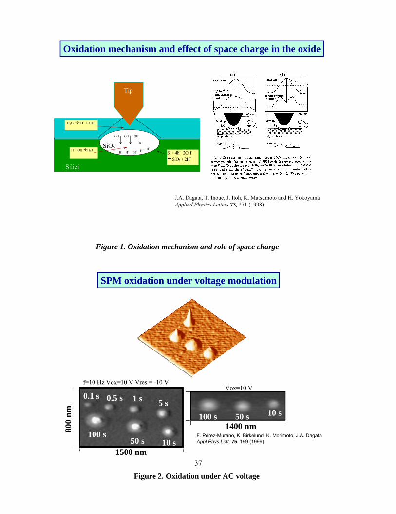
Oxidation mechanism and effect of space charge in the oxide
J.A. Dagata, T. Inoue, J. Itoh, K. Matsumoto and H. YokoyamaApplied Physics Letters 73, 271 (1998)
Figure 1. Oxidation mechanism and role of space charge
371500 nm
0.1 s5 s
10 s100 s
50 s
1 s0.5 s
800
nm
1400 nm10 s100 s 50 s
f=10 Hz Vox=10 V Vres = -10 VVox=10 V
F. Pérez-Murano, K. Birkelund, K. Morimoto, J.A. DagataAppl.Phys.Lett. 75, 199 (1999)
SPM oxidation under voltage modulation
Figure 2. Oxidation under AC voltage
1.0µm
+ +
– –
2.0µm
Non contact SPM nano-oxidation
Environmental SEM images of the meniscus:M. Schenk, M. Futing, and R. Reichelt. J. Appl. Phys. 84, 4880 (1998)
Figure 3. When performing the oxidation in non-contact, varying the tip-sample
distance can control the width of the oxidation
Preliminary measurements of current detection
-5 0 5 10 15 20 25 30 35 40 45-25
-20
-15
-10
-5
0
5
Def
lect
ion
(nm
)
Z displacement (nm)
0 10 20 30 40
0
5
10
15
Cur
rent
(pA
)
Z displacement (nm)
0.00 0.05 0.10 0.15 0.20 0.25 0.30 0.351E-3
0.01
0.1
1
10
100
6.1V 6.4V 6.9V 7.3V 7.85V 9.3V
Cur
rent
(pA
)
time (s)0.00 0.05 0.10 0.15 0.20 0.25 0.30 0.35
-100
102030405060708090
100110
6.1V 6.4V 6.9V 7.3V 7.85V 9.3V
Curr
ent (
pA)
Time (s)
Cur11
0 500 1000
1E-3
0.01
0.1
1
10 cur12-13 5.9V cur11-44 6.1V cur11-50 6.9V cur12-15 6.4V
curre
nt (p
A)
time(ms)
0 200 400 600 800 10001E-3
0.01
0.1
1
10
Cur12-135.9V
curr
ent (
pA)
time(ms) 0 200 400 600 800 10001E-3
0.01
0.1
1
10
Cur12-156.4V
curr
ent (
pA)
time(ms)
Figure 4. Current detection during oxidation
38
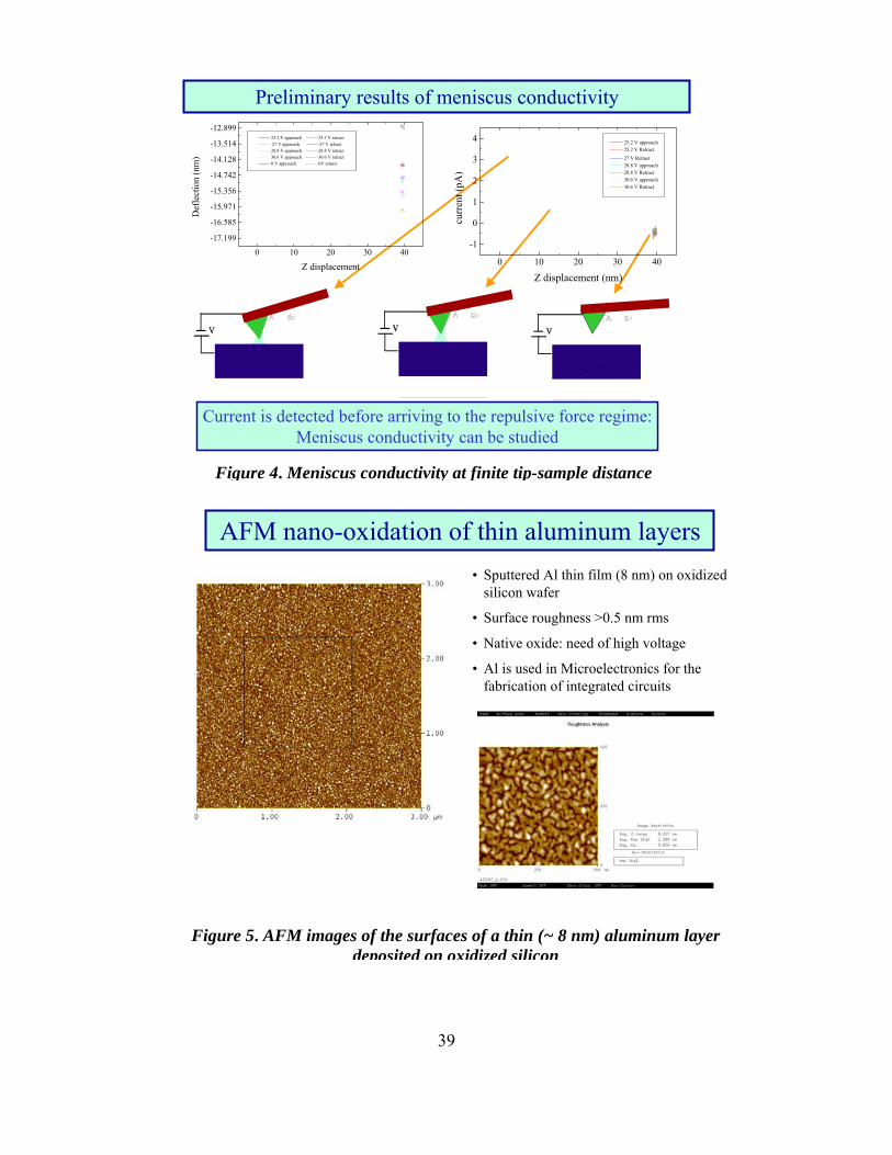
Preliminary results of meniscus conductivity
0 10 20 30 40
-17.199
-16.585
-15.971
-15.356
-14.742
-14.128
-13.514
-12.899 25.2 V approach 25.2 V retract 27 V approach 27 V retract 28.8 V approach 28.8 V retract 30.6 V approach 30.6 V retract 0 V approach 0V retract
Def
lect
ion
(nm
)
Z displacement 0 10 20 30 40
-1
0
1
2
3
4 25.2 V approach 25.2 V Retract 27 V Retract 28.8 V approach 28.8 V Retract 30.6 V approach 30.6 V Retract
curr
ent (
pA)
Z displacement (nm)
Current is detected before arriving to the repulsive force regime:Meniscus conductivity can be studied
Figure 4. Meniscus conductivity at finite tip-sample distance
AFM nano-oxidation of thin aluminum layers• Sputtered Al thin film (8 nm) on oxidized
silicon wafer
• Surface roughness >0.5 nm rms
• Native oxide: need of high voltage
• Al is used in Microelectronics for thefabrication of integrated circuits
Figure 5. AFM images of the surfaces of a thin (~ 8 nm) aluminum layer deposited on oxidized silicon
39
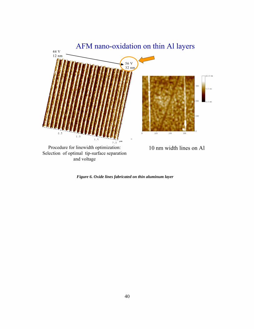
44 V12 nm
56 V32 nm
AFM nano-oxidation on thin Al layers
Procedure for linewidth optimization:Selection of optimal tip-surface separation
and voltage
10 nm width lines on Al
Figure 6. Oxide lines fabricated on thin aluminum layer
40
In-situ current measurement during dot formation on H-passivated p-Si(001)
Hiromi Kuramochi and Hiroshi Yokoyama*
Research Consortium for Synthetic Nano-Function Materials Project (SYNAF)-SII, 1-1-1 Higashi, Tsukuba,
Ibaraki 305-8562, Japan *SYNAF- National Institute of Advanced Industrial Science and Technology (AIST), 1-1-1 Umezono, Tsukuba, Ibaraki 305-
8568, Japan
Nanometer-scale oxidation by atomic force microscope (AFM) -based method has been established in this decade and now it is a popular technique to fabricate nanostructures. The size of the structures decreased, the pattern became complicated and various materials have been used as objects. Understanding the nano-oxidation process is increased by development of study on kinetics and mechanism, such as the kinetic oxide growth model [1], steady-state model based on in situ electrical force characterization by scanning Maxwell stress microscopy [2] and water meniscus model for noncontact-AFM [3]. It is clear that direct monitoring of oxidation process is necessary for achieving further understanding of kinetics and precise control. Here, in situ current detection during nano-oxidation in contact mode will be reported. The sample was p-Si(001) with a resistivity of 1-10 Ω·cm and it was passivated by hydrogen using HF solution. Experiments were carried out at room temperature using an environmental control AFM (SII, SPA-300HV) which is combined with a humidity regulator. The humidity in the AFM chamber is controllable from 30-80 % with an accuracy of 1 %. The AFM based on the optical lever system [4] to measure the deflection of the cantilever. The conductive cantilever with microfabricated Si tip is coated with Rh. Soft cantilevers with the nominal spring constants of 0.2N/m were used for current detection during dot fabrication and a bit stiffer ones (1.6 N/m) were current detection during force curve measurements.
41
40
30
20
10
cunt
(pA
)rr
e
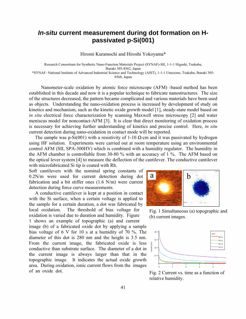
A conductive cantilever is kept at a position in contact with the Si surface, when a certain voltage is applied to the sample for a certain duration, a dot was fabricated by local oxidation. The threshold of bias voltage for oxidation is varied due to duration and humidity. Figure 1 shows an example of topographic (a) and current image (b) of a fabricated oxide dot by applying a sample bias voltage of 6 V for 10 s at a humidity of 70 %. The diameter of this dot is 280 nm and the height is 3.5 nm. From the current image, the fabricated oxide is less conductive than substrate surface. The diameter of a dot in the current image is always larger than that in the topographic image. It indicates the actual oxide growth area. During oxidation, ionic current flows from the images of an oxide dot.
Fig. 1 Simultaneous (a) topographic and (b) current images.
8642
10 V
50 %
60 %
40 %
70 %
0e (s)tim
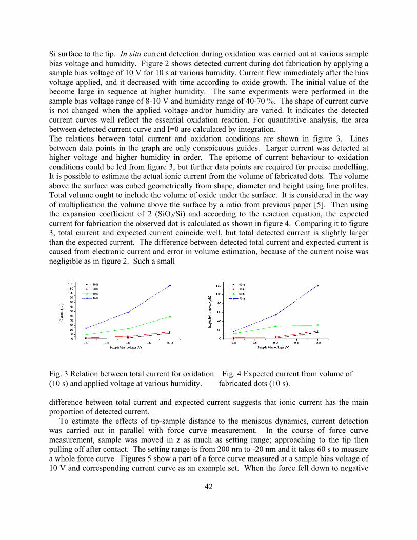
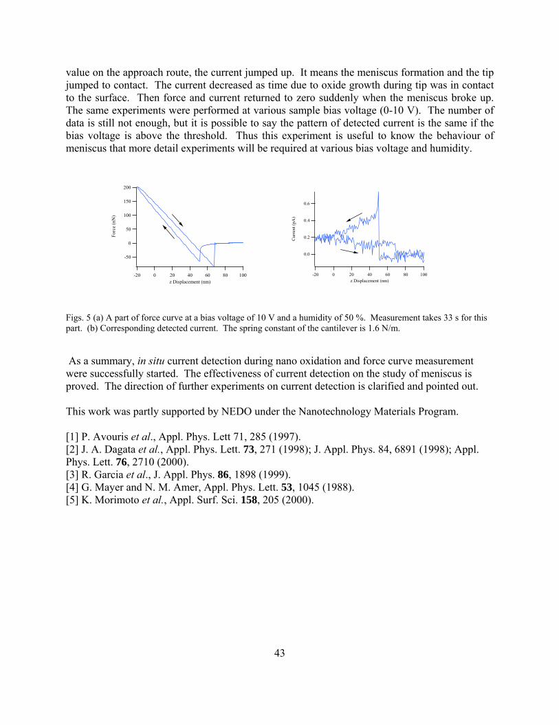
Fig. 2 Current vs. time as a function of relative humidity.
Si surface to the tip. In situ current detection during oxidation was carried out at various sample bias voltage and humidity. Figure 2 shows detected current during dot fabrication by applying a sample bias voltage of 10 V for 10 s at various humidity. Current flew immediately after the bias voltage applied, and it decreased with time according to oxide growth. The initial value of the become large in sequence at higher humidity. The same experiments were performed in the sample bias voltage range of 8-10 V and humidity range of 40-70 %. The shape of current curve is not changed when the applied voltage and/or humidity are varied. It indicates the detected current curves well reflect the essential oxidation reaction. For quantitative analysis, the area between detected current curve and I=0 are calculated by integration. The relations between total current and oxidation conditions are shown in figure 3. Lines between data points in the graph are only conspicuous guides. Larger current was detected at higher voltage and higher humidity in order. The epitome of current behaviour to oxidation conditions could be led from figure 3, but further data points are required for precise modelling. It is possible to estimate the actual ionic current from the volume of fabricated dots. The volume above the surface was cubed geometrically from shape, diameter and height using line profiles. Total volume ought to include the volume of oxide under the surface. It is considered in the way of multiplication the volume above the surface by a ratio from previous paper [5]. Then using the expansion coefficient of 2 (SiO2/Si) and according to the reaction equation, the expected current for fabrication the observed dot is calculated as shown in figure 4. Comparing it to figure 3, total current and expected current coincide well, but total detected current is slightly larger than the expected current. The difference between detected total current and expected current is caused from electronic current and error in volume estimation, because of the current noise was negligible as in figure 2. Such a small Fig. 3 Relation between total current for oxidation Fig. 4 Expected current from volume of (10 s) and applied voltage at various humidity. fabricated dots (10 s). difference between total current and expected current suggests that ionic current has the main proportion of detected current. To estimate the effects of tip-sample distance to the meniscus dynamics, current detection was carried out in parallel with force curve measurement. In the course of force curve measurement, sample was moved in z as much as setting range; approaching to the tip then pulling off after contact. The setting range is from 200 nm to -20 nm and it takes 60 s to measure a whole force curve. Figures 5 show a part of a force curve measured at a sample bias voltage of 10 V and corresponding current curve as an example set. When the force fell down to negative
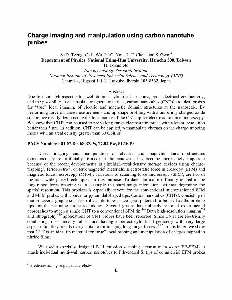
42
value on the approach route, the current jumped up. It means the meniscus formation and the tip jumped to contact. The current decreased as time due to oxide growth during tip was in contact to the surface. Then force and current returned to zero suddenly when the meniscus broke up. The same experiments were performed at various sample bias voltage (0-10 V). The number of data is still not enough, but it is possible to say the pattern of detected current is the same if the bias voltage is above the threshold. Thus this experiment is useful to know the behaviour of meniscus that more detail experiments will be required at various bias voltage and humidity. 200
150
100
50
0
-50
Forc
e (n
N)
100806040200-20z Displacement (nm)
0.6
0.4
0.2
0.0
Cur
rent
(pA
)
100806040200-20z Displacement (nm)
Figs. 5 (a) A part of force curve at a bias voltage of 10 V and a humidity of 50 %. Measurement takes 33 s for this part. (b) Corresponding detected current. The spring constant of the cantilever is 1.6 N/m. As a summary, in situ current detection during nano oxidation and force curve measurement were successfully started. The effectiveness of current detection on the study of meniscus is proved. The direction of further experiments on current detection is clarified and pointed out. This work was partly supported by NEDO under the Nanotechnology Materials Program. [1] P. Avouris et al., Appl. Phys. Lett 71, 285 (1997). [2] J. A. Dagata et al., Appl. Phys. Lett. 73, 271 (1998); J. Appl. Phys. 84, 6891 (1998); Appl. Phys. Lett. 76, 2710 (2000). [3] R. Garcia et al., J. Appl. Phys. 86, 1898 (1999). [4] G. Mayer and N. M. Amer, Appl. Phys. Lett. 53, 1045 (1988). [5] K. Morimoto et al., Appl. Surf. Sci. 158, 205 (2000).
43

44
45
Charge imaging and manipulation using carbon nanotube probes
S.-D. Tzeng, C.-L. Wu, Y.-C. You, T. T. Chen, and S. Gwoa)
Department of Physics, National Tsing-Hua University, Hsinchu 300, Taiwan H. Tokumoto
Nanotechnology Research Institute National Institute of Advanced Industrial Science and Technology (AIST)
Central-4, Higashi 1-1-1, Tsukuba, Ibaraki 305-8562, Japan
Abstract Due to their high aspect ratio, well-defined cylindrical structure, good electrical conductivity, and the possibility to encapsulate magnetic materials, carbon nanotubes (CNTs) are ideal probes for “true” local imaging of electric and magnetic domain structures at the nanoscale. By performing force-distance measurements and tip-shape profiling with a uniformly charged oxide square, we clearly demonstrate the local nature of the CNT tip for electrostatic force microscopy. We show that CNTs can be used to probe long-range electrostatic forces with a lateral resolution better than 5 nm. In addition, CNT can be applied to manipulate charges on the charge-trapping media with an areal density greater than 60 Gbit/in2. PACS Numbers: 81.07.De, 68.37.Ps, 77.84.Bw, 81.16.Pr
Direct imaging and manipulation of electric and magnetic domain structures (spontaneously or artificially formed) at the nanoscale has become increasingly important because of the recent developments in ultrahigh-areal-density storage devices using charge-trapping1, ferroelectric2, or ferromagnetic3 materials. Electrostatic force microscopy (EFM) and magnetic force microscopy (MFM), variations of scanning force microscopy (SFM), are two of the most widely used techniques for this purpose. To date, the major difficulty related to the long-range force imaging is to decouple the short-range interactions without degrading the spatial resolution. This problem is especially severe for the conventional micromachined EFM and MFM probes with conical or pyramidal shaped tips. Carbon nanotubes (CNTs), consisting of one or several graphene sheets rolled into tubes, have great potential to be used as the probing tips for the scanning probe techniques. Several groups have already reported experimental approaches to attach a single CNT to a conventional SFM tip.4-6 Both high-resolution imaging7,8 and lithography9,10 applications of CNT probes have been reported. Since CNTs are electrically conducting, mechanically robust, and having a perfect cylindrical geometry with very large aspect ratio, they are also very suitable for imaging long-range forces.11,12 In this letter, we show that CNT is an ideal tip material for “true” local probing and manipulation of charges trapped in nitride films.
We used a specially designed field emission scanning electron microscope (FE-SEM) to attach individual multi-wall carbon nanotubes to PtIr-coated Si tips of commercial EFM probes
a) Electronic mail: [email protected]
46
(~70 kHz resonance frequency and ~2.8 N/m force constant, and ~10-15 μm tip length). To separate the electrostatic force information from the total interaction of probe and sample, we used a dual-modulation scheme (operating in the dynamic mode), where a near-resonant mechanical modulation (ωm ≈ ω0 ≈ 70 kHz) was applied to the cantilever and a non-resonant electric modulation (ωe, ≈ 20 kHz) was applied to the sample bias voltage. The average tip-sample separation (dynamic mode) used in this study was ~15-30 nm. Two types of charge-storage media were used in this work for EFM imaging. One type consists of a Si3N4/SiO2 bilayer (4-nm/3-nm thickness); and the other is a single Si3N4 layer (3.5-nm thickness), both grown on p-type Si(001) substrates. For both types of samples, the nitride layer was used as the charge-trapping layer and was deposited by conventional low-pressure chemical vapor deposition.
Figure 1(a) shows dynamic force-distance curves of PtIr-coated Si tip and CNT-attached tip measured by the same type of EFM probes on a gold film in air. And, Fig. 1(b) shows quasistatic force-displacement curves used to determine the closest tip-sample distances before the tip snap-in. The drastic difference in the contact force (surface adhesion due to the absorbed humidity layer) between these two types of tips can be directly observed in Fig. 1(b). From the measurement shown in Fig 1(a), we can confirm that the force-distance relationship of a conventional EFM probe with a metal-coated Si tip is in qualitative agreement with the results simulated by S. Belaidi et al.13 We can use a sphere/cone/cantilever probe geometry to understand the measurement results of a conventional EFM probe. In the large-distance regime (tip-sample distance >10 μm), the detected electrostatic force is mainly a long-range capacitive force resulting from the cantilever and the Au sample. In the intermediate regime (<10 μm), the electrostatic force between the tip cone and the Au sample begins to contribute significantly to the detected force. Only in the proximate regime (<40 nm), the main detected electrostatic force is from the interaction between the tip apex and the sample. However, in this regime, van der Waals and various chemical interactions also become dominant. Therefore, to separate these interactions between the sample and the conventional Si tip, the conventional approach is to “lift” the tip above the sample some tens of nanometers. However, in this case, reduction in lateral resolution would occur due to the increase in the tip-to-sample distance and the occurrence of electrostatic interaction between the sample and the cone structure of Si tip. By contrast, the force-distance curve of CNT-attached tip shows much less contribution from the Si cone structure in a wide range of tip-sample distance. This is the main reason why CNT probes enable “true” local sensing of electrostatic interactions under typical noncontact or intermittent-contact operating conditions. Two dotted lines in the CNT force curve of Fig. 1(a) shows the regions of interaction transition. The actual CNT length (~380 nm) acquired by FE-SEM imaging is also indicated in the curve. The measured power-law exponents for force versus tip-sample distance are: –1 (∝ 1/d) for the spherical tip apex of the conventional probe and –0.45 for the nanotube, while the exponent for the common tip cone structure is –0.25, which are consistent with the expected sphere-like, rod-like, and cone-like behaviour, respectively.
For nitride charging experiments performed on nitride films in air, we have previously discovered14 that anodic oxidation could occur in the proximity of the local probe due to the intense electric field built between the grounded probe and the humidity-layer-covered nitride film on top of a positively biased Si substrate. We have found that the main oxidation by-product
47
ions (positive charge state) could be trapped at the anodic-oxide/nitride interface with a long retention time. Therefore, a well-prepared oxide pattern on nitride can be used as a uniformly charged “mirror” for imaging the tip shapes of EFM probes. Figure 2 shows an example of such experiments on an oxide-nitride-oxide-silicon (ONOS) structure with two types of probes. A positively charged oxide square was prepared by locally oxidizing the Si3N4/SiO2 bilayer film using a conducting probe under ambient conditions. Instead of the centre-protruded EFM image taken with a conventional EFM probe, using a CNT probe, we can resolve the sharp boundary of the charged and uncharged regions and the electrostatic force signal is quite uniform within the charged region.
To obtain the information of optimum resolution for EFM imaging with a CNT-probe, an array of alternative positively and negatively charged regions was written in a Si3N4 film with ±10 V voltage pulses (1-ms-width for the PtIr-coated Si tip and 1-s-width for the CNT tip) applied between the conducting tip and the p-type Si substrate, as shown in Fig. 3. In order to avoid the complication of field-induced oxidation and charge trapping occurred in ambient air, the local charging experiments were performed in high vacuum (~10-6 Torr) with an environment-controlled SFM system (SPA300HV, Seiko Instruments) such that field-induced anodic oxidation did not occur during the charging and subsequent imaging process. We found that the topographic images taken with the CNT probe displays much finer topographic features of the nitride surface with small feature sizes of the order of ~5-nm. Since the Z-feedback of the probe position is controlled by the surface topography and the electrostatic force signal corresponds to the interaction of the tip with the bulk charge trapping sites within the nitride film, the “true” local sensing of electrostatic force should reflect the local surface topography because that the tip moves conformably with the surface topography during simultaneous EFM imaging and the effective probed volume of bulk charged sites should change accordingly. This is observed only with the EFM image using the CNT probe because of its local probing capability. By comparing the fine features displayed in Figs. 3(d) and 3(e), the achievable EFM resolution using a CNT probe is determined to be better than 5 nm. In contrast to the much improved lateral resolution, the EFM signal obtained with the CNT probe is weaker due to the effective probed sample volume is much smaller than that of the conventional probe. This is consistent with the line profiles of EFM images shown in Fig. 2(e).
The areal bit density of the charged array demonstrated here is ~64 Gbit/in2 and the charged regions are erasable and rewritable by applying reverse voltages. From the known trap density of electron or hole in Si3N4 film, we estimate that each charged bit contains a few tens of electrons or holes. It is interesting to note that although CNT probes can provide an extremely high lateral resolution for EFM imaging, the charged dot diameter induced by the CNT tip is not significantly smaller than that induced by the tip of a conventional EFM probe (45-50 nm vs. 60-65 nm). The reason might be that, during the writing process, the intensive charging field causes significant lateral relaxation of the trapped charges similar to the known phenomenon of electric-field-induced thermal excitation of trapped charge carriers at room temperature.15 Although we demonstrate only the capabilities of imaging and manipulation of charges on insulating films, the drastic improved spatial resolution of EFM imaging with single CNT tips can open up new applications of nanometer-scale surface potential measurements. This is especially important for studying individual nanomaterials such as nanocrystals,16 CNTs,17 or even biological samples.

48
We thank the National Science Council (NSC) in Taiwan and the Program for Promoting Academic Excellence of Universities, the Ministry of Education (MOE) in Taiwan for supporting this research and J. A. Dagata for enlightening discussions. The SEM manipulation work performed in AIST, Tsukuba was partially supported by the New Energy and Industrial Technology Development Organization (NEDO), Japan.
49
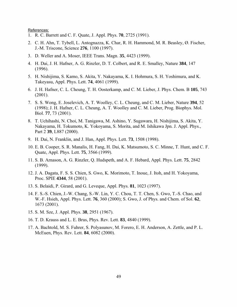
References:1. R. C. Barrett and C. F. Quate, J. Appl. Phys. 70, 2725 (1991).
2. C. H. Ahn, T. Tybell, L. Antognazza, K. Char, R. H. Hammond, M. R. Beasley, Ø. Fischer, J.-M. Triscone, Science 276, 1100 (1997).
3. D. Weller and A. Moser, IEEE Trans. Magn. 35, 4423 (1999).
4. H. Dai, J. H. Hafner, A. G. Rinzler, D. T. Colbert, and R. E. Smalley, Nature 384, 147 (1996).
5. H. Nishijima, S. Kamo, S. Akita, Y. Nakayama, K. I. Hohmura, S. H. Yoshimura, and K. Takeyasu, Appl. Phys. Lett. 74, 4061 (1999).
6. J. H. Hafner, C. L. Cheung, T. H. Oosterkamp, and C. M. Lieber, J. Phys. Chem. B 105, 743 (2001).
7. S. S. Wong, E. Joselevich, A. T. Woolley, C. L. Cheung, and C. M. Lieber, Nature 394, 52 (1998); J. H. Hafner, C. L. Cheung, A. T. Woolley and C. M. Lieber, Prog. Biophys. Mol. Biol. 77, 73 (2001).
8. T. Uchihashi, N. Choi, M. Tanigawa, M. Ashino, Y. Sugawara, H. Nishijima, S. Akita, Y. Nakayama, H. Tokumoto, K. Yokoyama, S. Morita, and M. Ishikawa Jpn. J. Appl. Phys., Part 2 39, L887 (2000).
9. H. Dai, N. Franklin, and J. Han, Appl. Phys. Lett. 73, 1508 (1998).
10. E. B. Cooper, S. R. Manalis, H. Fang, H. Dai, K. Matsumoto, S. C. Minne, T. Hunt, and C. F. Quate, Appl. Phys. Lett. 75, 3566 (1999).
11. S. B. Arnason, A. G. Rinzler, Q. Hudspeth, and A. F. Hebard, Appl. Phys. Lett. 75, 2842 (1999).
12. J. A. Dagata, F. S. S. Chien, S. Gwo, K. Morimoto, T. Inoue, J. Itoh, and H. Yokoyama, Proc. SPIE 4344, 58 (2001).
13. S. Belaidi, P. Girard, and G. Leveque, Appl. Phys. 81, 1023 (1997).
14. F. S.-S. Chien, J.-W. Chang, S.-W. Lin, Y. C. Chou, T. T. Chen, S. Gwo, T.-S. Chao, and W.-F. Hsieh, Appl. Phys. Lett. 76, 360 (2000); S. Gwo, J. of Phys. and Chem. of Sol. 62, 1673 (2001).
15. S. M. Sze, J. Appl. Phys. 38, 2951 (1967).
16. T. D. Krauss and L. E. Brus, Phys. Rev. Lett. 83, 4840 (1999).
17. A. Bachtold, M. S. Fuhrer, S. Polyasunov, M. Forero, E. H. Anderson, A. Zettle, and P. L. McEuen, Phys. Rev. Lett. 84, 6082 (2000).
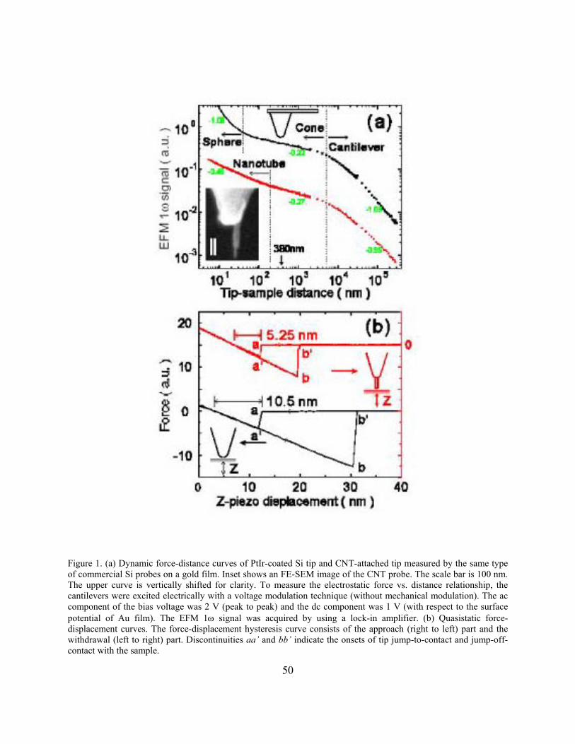
Figure 1. (a) Dynamic force-distance curves of PtIr-coated Si tip and CNT-attached tip measured by the same type of commercial Si probes on a gold film. Inset shows an FE-SEM image of the CNT probe. The scale bar is 100 nm. The upper curve is vertically shifted for clarity. To measure the electrostatic force vs. distance relationship, the cantilevers were excited electrically with a voltage modulation technique (without mechanical modulation). The ac component of the bias voltage was 2 V (peak to peak) and the dc component was 1 V (with respect to the surface potential of Au film). The EFM 1ω signal was acquired by using a lock-in amplifier. (b) Quasistatic force-displacement curves. The force-displacement hysteresis curve consists of the approach (right to left) part and the withdrawal (left to right) part. Discontinuities aa’ and bb’ indicate the onsets of tip jump-to-contact and jump-off-contact with the sample.
50
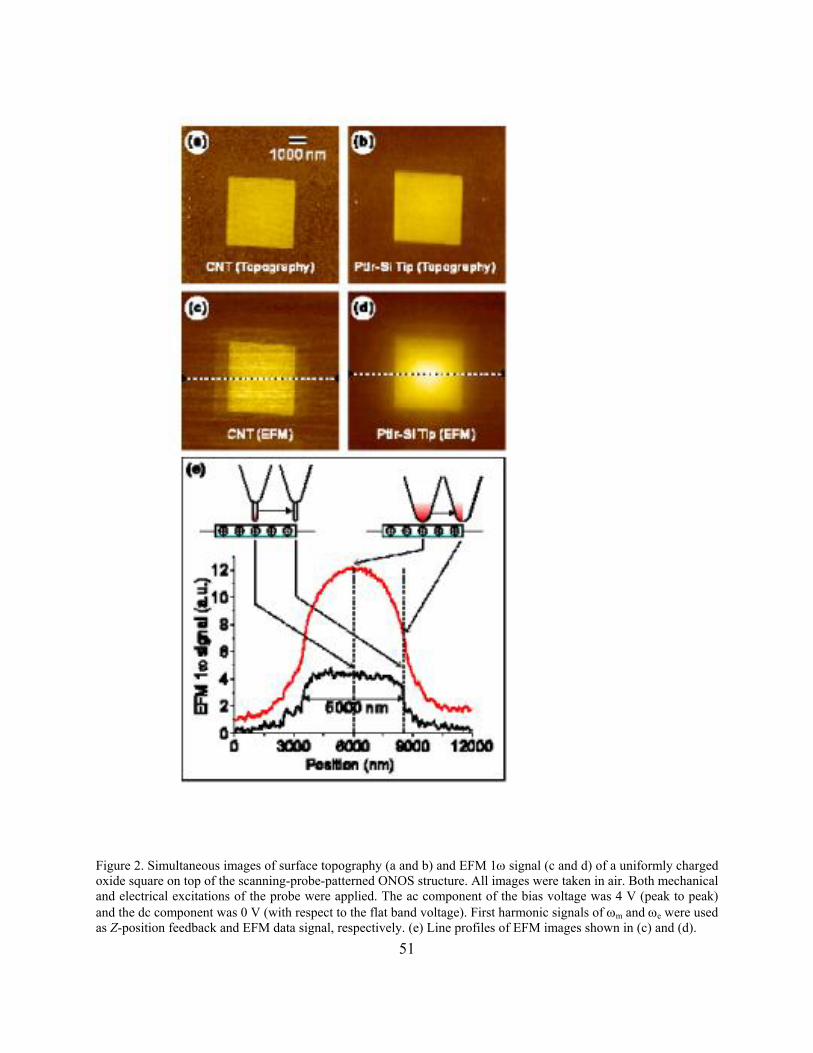
Figure 2. Simultaneous images of surface topography (a and b) and EFM 1ω signal (c and d) of a uniformly charged oxide square on top of the scanning-probe-patterned ONOS structure. All images were taken in air. Both mechanical and electrical excitations of the probe were applied. The ac component of the bias voltage was 4 V (peak to peak) and the dc component was 0 V (with respect to the flat band voltage). First harmonic signals of ωm and ωe were used as Z-position feedback and EFM data signal, respectively. (e) Line profiles of EFM images shown in (c) and (d). 51
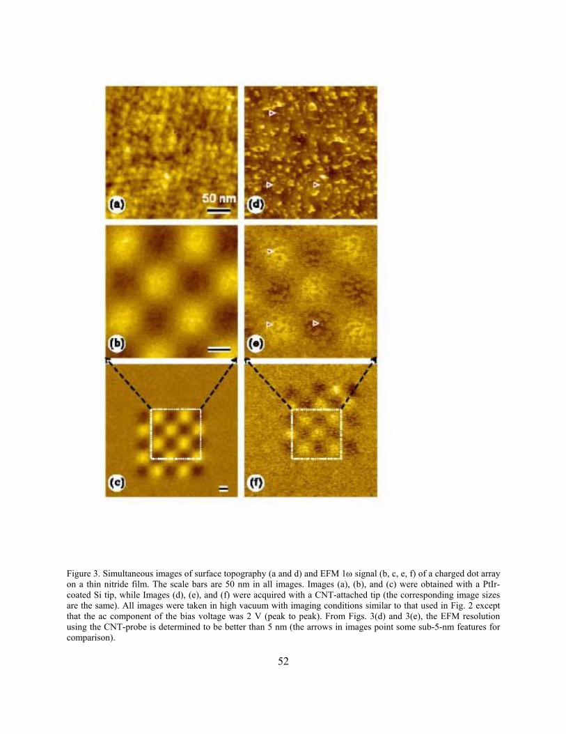
Figure 3. Simultaneous images of surface topography (a and d) and EFM 1ω signal (b, c, e, f) of a charged dot array on a thin nitride film. The scale bars are 50 nm in all images. Images (a), (b), and (c) were obtained with a PtIr-coated Si tip, while Images (d), (e), and (f) were acquired with a CNT-attached tip (the corresponding image sizes are the same). All images were taken in high vacuum with imaging conditions similar to that used in Fig. 2 except that the ac component of the bias voltage was 2 V (peak to peak). From Figs. 3(d) and 3(e), the EFM resolution using the CNT-probe is determined to be better than 5 nm (the arrows in images point some sub-5-nm features for comparison).
52
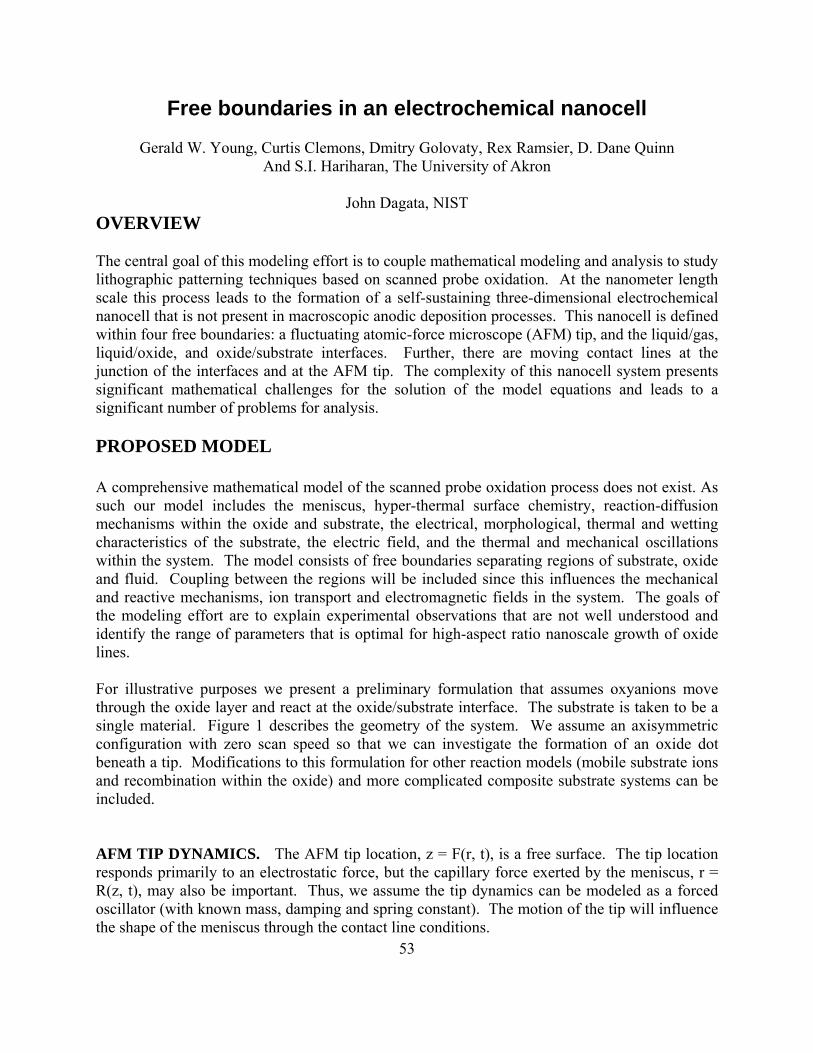
53
Free boundaries in an electrochemical nanocell
Gerald W. Young, Curtis Clemons, Dmitry Golovaty, Rex Ramsier, D. Dane Quinn And S.I. Hariharan, The University of Akron
John Dagata, NIST
OVERVIEW The central goal of this modeling effort is to couple mathematical modeling and analysis to study lithographic patterning techniques based on scanned probe oxidation. At the nanometer length scale this process leads to the formation of a self-sustaining three-dimensional electrochemical nanocell that is not present in macroscopic anodic deposition processes. This nanocell is defined within four free boundaries: a fluctuating atomic-force microscope (AFM) tip, and the liquid/gas, liquid/oxide, and oxide/substrate interfaces. Further, there are moving contact lines at the junction of the interfaces and at the AFM tip. The complexity of this nanocell system presents significant mathematical challenges for the solution of the model equations and leads to a significant number of problems for analysis. PROPOSED MODEL A comprehensive mathematical model of the scanned probe oxidation process does not exist. As such our model includes the meniscus, hyper-thermal surface chemistry, reaction-diffusion mechanisms within the oxide and substrate, the electrical, morphological, thermal and wetting characteristics of the substrate, the electric field, and the thermal and mechanical oscillations within the system. The model consists of free boundaries separating regions of substrate, oxide and fluid. Coupling between the regions will be included since this influences the mechanical and reactive mechanisms, ion transport and electromagnetic fields in the system. The goals of the modeling effort are to explain experimental observations that are not well understood and identify the range of parameters that is optimal for high-aspect ratio nanoscale growth of oxide lines. For illustrative purposes we present a preliminary formulation that assumes oxyanions move through the oxide layer and react at the oxide/substrate interface. The substrate is taken to be a single material. Figure 1 describes the geometry of the system. We assume an axisymmetric configuration with zero scan speed so that we can investigate the formation of an oxide dot beneath a tip. Modifications to this formulation for other reaction models (mobile substrate ions and recombination within the oxide) and more complicated composite substrate systems can be included. AFM TIP DYNAMICS. The AFM tip location, z = F(r, t), is a free surface. The tip location responds primarily to an electrostatic force, but the capillary force exerted by the meniscus, r = R(z, t), may also be important. Thus, we assume the tip dynamics can be modeled as a forced oscillator (with known mass, damping and spring constant). The motion of the tip will influence the shape of the meniscus through the contact line conditions.
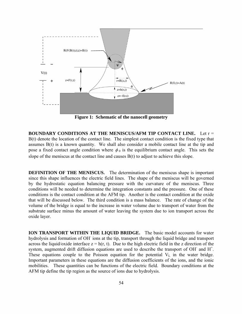
Figure 1: Schematic of the nanocell geometry
BOUNDARY CONDITIONS AT THE MENISCUS/AFM TIP CONTACT LINE. Let r = B(t) denote the location of the contact line. The simplest contact condition is the fixed type that assumes B(t) is a known quantity. We shall also consider a mobile contact line at the tip and pose a fixed contact angle condition where φ 0 is the equilibrium contact angle. This sets the slope of the meniscus at the contact line and causes B(t) to adjust to achieve this slope. DEFINITION OF THE MENISCUS. The determination of the meniscus shape is important since this shape influences the electric field lines. The shape of the meniscus will be governed by the hydrostatic equation balancing pressure with the curvature of the meniscus. Three conditions will be needed to determine the integration constants and the pressure. One of these conditions is the contact condition at the AFM tip. Another is the contact condition at the oxide that will be discussed below. The third condition is a mass balance. The rate of change of the volume of the bridge is equal to the increase in water volume due to transport of water from the substrate surface minus the amount of water leaving the system due to ion transport across the oxide layer. ION TRANSPORT WITHIN THE LIQUID BRIDGE. The basic model accounts for water hydrolysis and formation of OH- ions at the tip, transport through the liquid bridge and transport across the liquid/oxide interface z = h(r, t). Due to the high electric field in the z direction of the system, augmented drift diffusion equations are used to describe the transport of OH- and H+. These equations couple to the Poisson equation for the potential VL in the water bridge. Important parameters in these equations are the diffusion coefficients of the ions, and the ionic mobilities. These quantities can be functions of the electric field. Boundary conditions at the AFM tip define the tip region as the source of ions due to hydrolysis. 54
Finally, at the liquid/oxide interface z = h(r, t) we develop boundary conditions that relate the concentration of OH- and H+ ions in the liquid bridge to that in the oxide. These expressions relate the motion of the oxide/liquid interface to the current densities at this location. There is a possibility that a buildup of OH- ions occurs in the liquid bridge ahead of this interface. Perhaps this buildup leads to significant reduction of ionic transport within the nanocell. ION TRANSPORT IN THE OXIDE LAYER. The governing equations are similar to the above. Further, if the substrate ions are included in the oxide layer then we must add a transport equation to the above set to track the concentration of these ions. REACTIONS AT THE OXIDE/SUBSTRATE INTERFACE. First we assume that the rate of growth of the oxide/substrate front z = -f(r, t) is proportional to the rate of the reaction at this front. Information about the reaction rate constant is needed. Other boundary conditions relate the motion of the oxide/substrate interface to the current density at the front. Finally, due to the reactions at the substrate surface, H+ ions are released as the oxide is formed. Hence, the reaction serves as a source of these ions and provides the boundary condition for H+. BOUNDARY CONDITIONS AT THE MENISCUS/OXIDE JUNCTION. First we have the conditions of contact that require the oxide/liquid, oxide/substrate, substrate, and meniscus to meet at A(t), the unknown location of the contact line or edge of the oxide layer. We also assume a contact-line mobility condition based upon deviations of the contact angle θ from the equilibrium contact angle of the meniscus at the oxide. This equation will be applied provided θ > θ equil. In this case the contact line will move radially outward. If this condition is not satisfied, then the contact line remains fixed. The latter condition is imposed so that the oxide edge does not recede. We complete the system of equations by requiring that the mass consumption of the substrate equal the mass increase of the oxide. Each of the physical phenomena described above is coupled to one or more of the others through free boundaries and reaction terms. The tip dynamics influence the meniscus region, which determines the ion transport, which finally drives the reactions at the oxidation interface. In addition, this problem is fully coupled, so that we may not simply solve for one effect to be used as a "forcing" for the next. The resulting analysis must therefore account for this two-way coupling, which is expected to play a significant role in the resulting performance of this system. SOLUTION AND ANALYSIS STRATEGIES. To understand the complex process depicted in Figure 1 it is essential to understand the dynamics in one dimension. This model will help to identify the nonlinear coupling between various physical entities, and guide the analysis of the more complex axisymmetric configuration. The multi-dimensional structure of the scanned lines has received relatively little attention in the literature as the focus has been on explaining the
55

56
self-limited vertical growth. We shall develop quasi-steady and thin-domain two-dimensional models for the system. A second axisymmetric strategy is to suppose that the oxide layer is modeled as a thin cylindrical disk beneath a cylindrical column of liquid. Throughout the model development and simulation we plan to continually revisit the models after comparing model predictions with experimental observations. The experimental investigations for current measurement within the nanocell are of particular interest for investigating the transport mechanisms and self-limited vertical growth of the oxide.
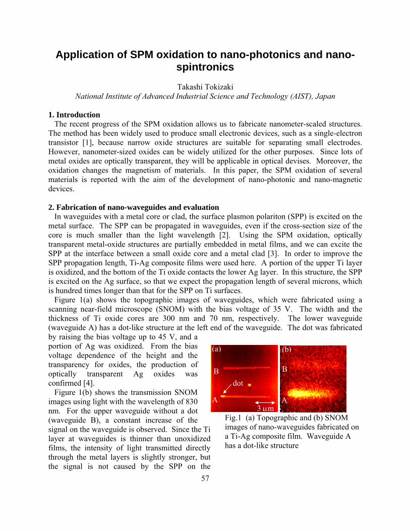
Application of SPM oxidation to nano-photonics and nano-spintronics
Takashi Tokizaki
National Institute of Advanced Industrial Science and Technology (AIST), Japan 1. Introduction The recent progress of the SPM oxidation allows us to fabricate nanometer-scaled structures. The method has been widely used to produce small electronic devices, such as a single-electron transistor [1], because narrow oxide structures are suitable for separating small electrodes. However, nanometer-sized oxides can be widely utilized for the other purposes. Since lots of metal oxides are optically transparent, they will be applicable in optical devises. Moreover, the oxidation changes the magnetism of materials. In this paper, the SPM oxidation of several materials is reported with the aim of the development of nano-photonic and nano-magnetic devices. 2. Fabrication of nano-waveguides and evaluation In waveguides with a metal core or clad, the surface plasmon polariton (SPP) is excited on the metal surface. The SPP can be propagated in waveguides, even if the cross-section size of the core is much smaller than the light wavelength [2]. Using the SPM oxidation, optically transparent metal-oxide structures are partially embedded in metal films, and we can excite the SPP at the interface between a small oxide core and a metal clad [3]. In order to improve the SPP propagation length, Ti-Ag composite films were used here. A portion of the upper Ti layer is oxidized, and the bottom of the Ti oxide contacts the lower Ag layer. In this structure, the SPP is excited on the Ag surface, so that we expect the propagation length of several microns, which is hundred times longer than that for the SPP on Ti surfaces. Figure 1(a) shows the topographic images of waveguides, which were fabricated using a scanning near-field microscope (SNOM) with the bias voltage of 35 V. The width and the thickness of Ti oxide cores are 300 nm and 70 nm, respectively. The lower waveguide (waveguide A) has a dot-like structure at the left end of the waveguide. The dot was fabricated by raising the bias voltage up to 45 V, and a portion of Ag was oxidized. From the bias voltage dependence of the height and the transparency for oxides, the production of optically transparent Ag oxides was confirmed [4]. Figure 1(b) shows the transmission SNOM images using light with the wavelength of 830 nm. For the upper waveguide without a dot (waveguide B), a constant increase of the signal on the waveguide is observed. Since the Ti layer at waveguides is thinner than unoxidized films, the intensity of light transmitted directly through the metal layers is slightly stronger, but the signal is not caused by the SPP on the
A
Bdot
B
A3 μm
(a) (b)
Fig.1 (a) Topographic and (b) SNOM images of nano-waveguides fabricated on a Ti-Ag composite film. Waveguide A has a dot-like structure
57
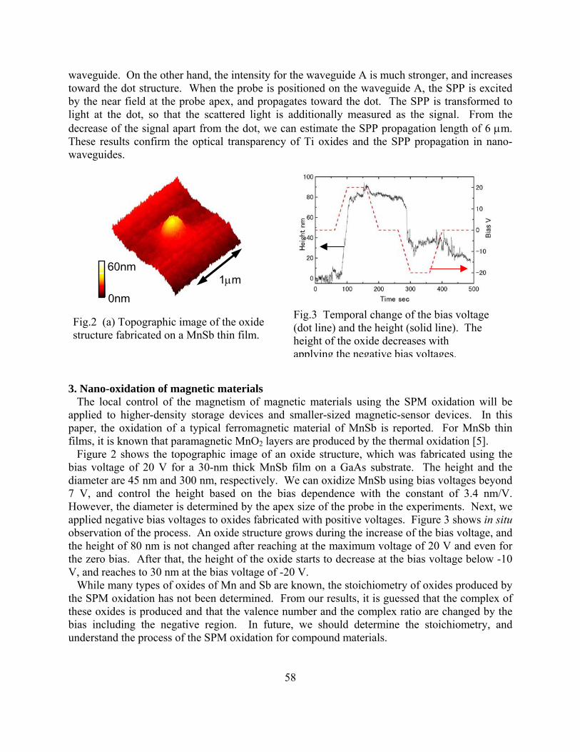
waveguide. On the other hand, the intensity for the waveguide A is much stronger, and increases toward the dot structure. When the probe is positioned on the waveguide A, the SPP is excited by the near field at the probe apex, and propagates toward the dot. The SPP is transformed to light at the dot, so that the scattered light is additionally measured as the signal. From the decrease of the signal apart from the dot, we can estimate the SPP propagation length of 6 μm. These results confirm the optical transparency of Ti oxides and the SPP propagation in nano-waveguides.
1μm0nm
60nm
Fig.2 (a) Topographic image of the oxide structure fabricated on a MnSb thin film.
Fig.3 Temporal change of the bias voltage (dot line) and the height (solid line). The height of the oxide decreases with applying the negative bias voltages.
3. Nano-oxidation of magnetic materials The local control of the magnetism of magnetic materials using the SPM oxidation will be applied to higher-density storage devices and smaller-sized magnetic-sensor devices. In this paper, the oxidation of a typical ferromagnetic material of MnSb is reported. For MnSb thin films, it is known that paramagnetic MnO2 layers are produced by the thermal oxidation [5]. Figure 2 shows the topographic image of an oxide structure, which was fabricated using the bias voltage of 20 V for a 30-nm thick MnSb film on a GaAs substrate. The height and the diameter are 45 nm and 300 nm, respectively. We can oxidize MnSb using bias voltages beyond 7 V, and control the height based on the bias dependence with the constant of 3.4 nm/V. However, the diameter is determined by the apex size of the probe in the experiments. Next, we applied negative bias voltages to oxides fabricated with positive voltages. Figure 3 shows in situ observation of the process. An oxide structure grows during the increase of the bias voltage, and the height of 80 nm is not changed after reaching at the maximum voltage of 20 V and even for the zero bias. After that, the height of the oxide starts to decrease at the bias voltage below -10 V, and reaches to 30 nm at the bias voltage of -20 V. While many types of oxides of Mn and Sb are known, the stoichiometry of oxides produced by the SPM oxidation has not been determined. From our results, it is guessed that the complex of these oxides is produced and that the valence number and the complex ratio are changed by the bias including the negative region. In future, we should determine the stoichiometry, and understand the process of the SPM oxidation for compound materials.
58
59
4. Summary The SPM oxidation was applied to several materials. For making optical nano-waveguides, the thickness of Ti oxides was controlled up to 100 nm, and also Ag layers under Ti oxides were oxidized. The propagation of the SPP in nano-waveguides was confirmed based on a near-field optical technique. Next, the oxidation of a ferromagnetic material of MnSb was reported. While the magnetism and the stoichiometry of oxides have not been determined, the phenomenon which is understood as the deoxidation was found. References [1] Y..Gotoh et al., Jpn. J. Appl. Phys., 41 (2002) 2578. [2] J.Takahara et al., Opt. Lett., 22 (1997) 321. [3] T.Onuki et al., Appl. Phys. Lett., 80 (2002) 4629. [4] T.Onuki et al., Jpn. J. Appl. Phys., 41 (2002) 6256 [5] H.Akinaga et al., Jpn. J. Appl. Phys., 35 (1996) L897.

60
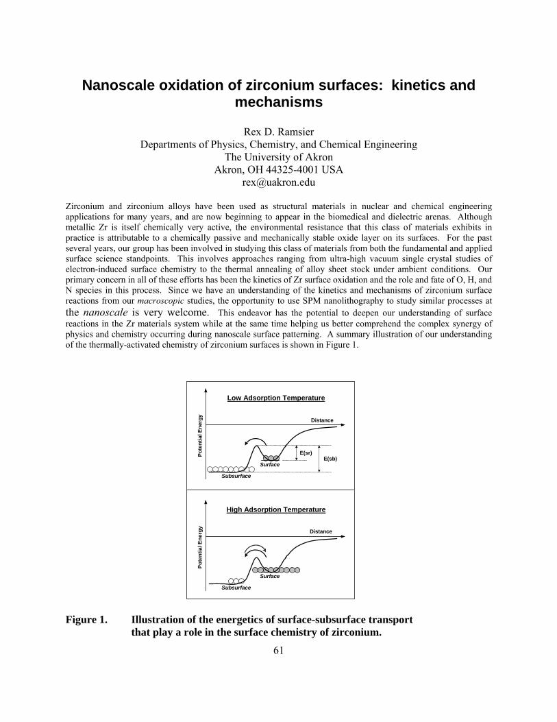
Nanoscale oxidation of zirconium surfaces: kinetics and mechanisms
Rex D. Ramsier
Departments of Physics, Chemistry, and Chemical Engineering The University of Akron
Akron, OH 44325-4001 USA [email protected]
Zirconium and zirconium alloys have been used as structural materials in nuclear and chemical engineering applications for many years, and are now beginning to appear in the biomedical and dielectric arenas. Although metallic Zr is itself chemically very active, the environmental resistance that this class of materials exhibits in practice is attributable to a chemically passive and mechanically stable oxide layer on its surfaces. For the past several years, our group has been involved in studying this class of materials from both the fundamental and applied surface science standpoints. This involves approaches ranging from ultra-high vacuum single crystal studies of electron-induced surface chemistry to the thermal annealing of alloy sheet stock under ambient conditions. Our primary concern in all of these efforts has been the kinetics of Zr surface oxidation and the role and fate of O, H, and N species in this process. Since we have an understanding of the kinetics and mechanisms of zirconium surface reactions from our macroscopic studies, the opportunity to use SPM nanolithography to study similar processes at the nanoscale is very welcome. This endeavor has the potential to deepen our understanding of surface reactions in the Zr materials system while at the same time helping us better comprehend the complex synergy of physics and chemistry occurring during nanoscale surface patterning. A summary illustration of our understanding of the thermally-activated chemistry of zirconium surfaces is shown in Figure 1.
Subsurface
Pote
ntia
l Ene
rgy
Distance
High Adsorption Temperature
Surface
Subsurface
Pote
ntia
l Ene
rgy
Distance
Low Adsorption Temperature
Surface
E(sr)E(sb)
Figure 1. Illustration of the energetics of surface-subsurface transport
that play a role in the surface chemistry of zirconium.
61
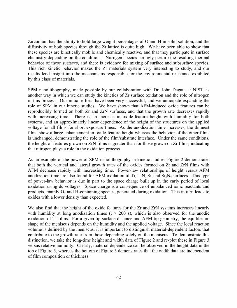
62
Zirconium has the ability to hold large weight percentages of O and H in solid solution, and the diffusivity of both species through the Zr lattice is quite high. We have been able to show that these species are kinetically mobile and chemically reactive, and that they participate in surface chemistry depending on the conditions. Nitrogen species strongly perturb the resulting thermal behavior of these surfaces, and there is evidence for mixing of surface and subsurface species. This rich kinetic behavior makes the Zr materials system very interesting to study, and our results lend insight into the mechanisms responsible for the environmental resistance exhibited by this class of materials. SPM nanolithography, made possible by our collaboration with Dr. John Dagata at NIST, is another way in which we can study the kinetics of Zr surface oxidation and the role of nitrogen in this process. Our initial efforts have been very successful, and we anticipate expanding the role of SPM in our kinetic studies. We have shown that AFM-induced oxide features can be reproducibly formed on both Zr and ZrN surfaces, and that the growth rate decreases rapidly with increasing time. There is an increase in oxide-feature height with humidity for both systems, and an approximately linear dependence of the height of the structures on the applied voltage for all films for short exposure times. As the anodization time increases, the thinnest films show a large enhancement in oxide-feature height whereas the behavior of the other films is unchanged, demonstrating the role of the film/substrate interface. Under the same conditions, the height of features grown on ZrN films is greater than for those grown on Zr films, indicating that nitrogen plays a role in the oxidation process. As an example of the power of SPM nanolithography in kinetic studies, Figure 2 demonstrates that both the vertical and lateral growth rates of the oxides formed on Zr and ZrN films with AFM decrease rapidly with increasing time. Power-law relationships of height versus AFM anodization time are also found for AFM oxidation of Ti, TiN, Si, and Si3N4 surfaces. This type of power-law behavior is due in part to the space charge built up in the early period of local oxidation using dc voltages. Space charge is a consequence of unbalanced ionic reactants and products, mainly O- and H-containing species, generated during oxidation. This in turn leads to oxides with a lower density than expected. We also find that the height of the oxide features for the Zr and ZrN systems increases linearly with humidity at long anodization times (t > 200 s), which is also observed for the anodic oxidation of Ti films. For a given tip-surface distance and AFM tip geometry, the equilibrium shape of the meniscus depends on the humidity and the applied voltage. Since the local reaction volume is defined by the meniscus, it is important to distinguish material-dependent factors that contribute to the growth rate from those depending solely on the meniscus. To demonstrate this distinction, we take the long-time height and width data of Figure 2 and re-plot these in Figure 3 versus relative humidity. Clearly, material dependence can be observed in the height data in the top of Figure 3, whereas the bottom of Figure 3 demonstrates that the width data are independent of film composition or thickness.
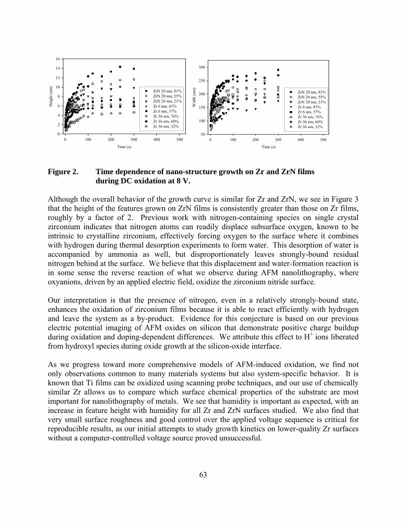
Time (s)
0 100 200 300 400 500
Hei
ght (
nm)
0
2
4
6
8
10
12
14
16
ZrN 20 nm, 81%ZrN 20 nm, 55%ZrN 20 nm, 21%Zr 6 nm, 43%Zr 6 nm, 37%Zr 36 nm, 76%Zr 36 nm, 60%Zr 36 nm, 32%
Time (s)
0 100 200 300 400 500
Wid
th (n
m)
50
100
150
200
250
300
ZrN 20 nm, 81%ZrN 20 nm, 55%ZrN 20 nm, 21%Zr 6 nm, 43%Zr 6 nm, 37%Zr 36 nm, 76%Zr 36 nm, 60%Zr 36 nm, 32%
Figure 2. Time dependence of nano-structure growth on Zr and ZrN films during DC oxidation at 8 V.
Although the overall behavior of the growth curve is similar for Zr and ZrN, we see in Figure 3 that the height of the features grown on ZrN films is consistently greater than those on Zr films, roughly by a factor of 2. Previous work with nitrogen-containing species on single crystal zirconium indicates that nitrogen atoms can readily displace subsurface oxygen, known to be intrinsic to crystalline zirconium, effectively forcing oxygen to the surface where it combines with hydrogen during thermal desorption experiments to form water. This desorption of water is accompanied by ammonia as well, but disproportionately leaves strongly-bound residual nitrogen behind at the surface. We believe that this displacement and water-formation reaction is in some sense the reverse reaction of what we observe during AFM nanolithography, where oxyanions, driven by an applied electric field, oxidize the zirconium nitride surface. Our interpretation is that the presence of nitrogen, even in a relatively strongly-bound state, enhances the oxidation of zirconium films because it is able to react efficiently with hydrogen and leave the system as a by-product. Evidence for this conjecture is based on our previous electric potential imaging of AFM oxides on silicon that demonstrate positive charge buildup during oxidation and doping-dependent differences. We attribute this effect to H+ ions liberated from hydroxyl species during oxide growth at the silicon-oxide interface. As we progress toward more comprehensive models of AFM-induced oxidation, we find not only observations common to many materials systems but also system-specific behavior. It is known that Ti films can be oxidized using scanning probe techniques, and our use of chemically similar Zr allows us to compare which surface chemical properties of the substrate are most important for nanolithography of metals. We see that humidity is important as expected, with an increase in feature height with humidity for all Zr and ZrN surfaces studied. We also find that very small surface roughness and good control over the applied voltage sequence is critical for reproducible results, as our initial attempts to study growth kinetics on lower-quality Zr surfaces without a computer-controlled voltage source proved unsuccessful.
63
Relative Humidity (%)
20 30 40 50 60 70 80
Hei
ght (
nm)
0
2
4
6
8
10
12
14
16
ZrN 20 nm
Zr 6 nm
Zr 36 nm
Relative Humidity (%)
20 30 40 50 60 70 80
Wid
th (n
m)
120
160
200
240
280
320
Data From All SamplesIn The Upper Panel
Figure 3. Humidity dependence of nano-structure growth on Zr and ZrN films during DC oxidation at 8 V. Our results for AFM-induced oxide growth on Zr and ZrN surfaces show kinetics similar to those seen in other metal and semiconductor systems, with generally similar feature dimensions and time/voltage characteristics. This would seem to indicate that the major factors influencing the growth are inherent to the method itself, and not to the details of the surface chemistry. This strengthens arguments that the AFM-based technique is transferable across materials systems, which greatly enhances its potential role in nano-fabrication technology. However, it also leads to fundamental questions as to why the results are somewhat insensitive to the surface chemistry which we know strongly depends on the material system in other contexts. The answer to these questions may lie in the presence of very high electric fields and a resulting dominance by hyperthermally-driven surface reactions involving ionic and radical species during AFM oxidation. Such species are not present during standard surface kinetic studies, and their concentration and flux at the surface even in normal electrochemical measurements is certainly much lower than in the nanolithography process. Recent Papers Related to AFM and Zirconium Surface Chemistry "Ultra-High Vacuum Investigation of the Surface Chemistry of Zirconium",
Y.C. Kang, M.M. Milovancev, D.A. Clauss, M.A. Lange and R.D. Ramsier, J. Nucl. Mater. 281, 57 (2000).
"SPM Tip-Sample Interactions in Primary Alcohols of Varying Chain Length",
R.M. Ralich, Y. Wu, R.D. Ramsier and P.N. Henriksen, J. Vac. Sci. Technol. A 18, 1345 (2000).
"The Behavior of Zirconium Surfaces in the Presence of Oxygen, Nitrogen, and
Hydrogen Containing Adsorbates", Y.C. Kang, D.A. Clauss and R.D. Ramsier, J. Vac. Sci. Technol. A 19, 1996 (2001).
64
65
"Nanolithography of Silicon: An Approach for Investigating Tip-Surface Interactions During Writing", R.D Ramsier, R.M. Ralich and S.F. Lyuksyutov, Appl. Phys. Lett. 79, 2820 (2001).
"The Adsorption of Ammonia on Zirconium Surfaces: Effect of Adsorption Temperature
on the Thermal Desorption of Water", Y.C. Kang and R.D. Ramsier, Vacuum 64, 113 (2002).
"Measuring and Modeling Thermal Fluctuations at Nanometer Length Scales",
R.M. Ralich, R.D. Ramsier, D.D. Quinn, C.B. Clemons, and G.W. Young,
Phys. Rev. E 65, 057601 (2002). "Optical and Structural Studies of Films Grown Thermally on Zirconium Surfaces",
J.M. Morgan, J.S. McNatt, M.J. Shepard, N. Farkas and R.D. Ramsier, J. Appl. Phys. 91, 9375 (2002).
"Investigation of Nitric Oxide Adsorption on Zr(0001)",
Y.C. Kang and R.D. Ramsier, J. Nucl. Mater. 303, 125 (2002).
"The Influence of Subsurface Species on Desorption Kinetics: 18O2/Zr(0001)",
Y.C. Kang and R.D. Ramsier, Appl. Surf. Sci. 195, 196 (2002).
"Non-destructive Characterization of Films Grown on Zircaloy-2 by Annealing in Air",
J.S. McNatt, M.J. Shepard, N. Farkas, J.M. Morgan and R.D. Ramsier, J. Phys. D: Appl. Phys. 35, 1855 (2002).
"Kinetic Effects of Subsurface Species on Zr(0001) Surface Chemistry",
Y.C. Kang and R.D. Ramsier, Surf. Sci., 519, 229 (2002).
"Ammonia Adsorption on Zr(0001): The Effect of Electron Bombardment
on Hydrogen Production", N. Stojilovic, Y.C. Kang and R.D. Ramsier, Surf. Interface. Anal., Accepted (2002).
"Electron Bombardment of Water Adsorbed on Zr(0001) Surfaces",
S. Ankrah, Y.C. Kang and R.D. Ramsier, J. Phys. C: Cond. Mater., Under Consideration.
"Nanoscale Oxidation of Zirconium Surfaces: Kinetics and Mechanisms",
N. Farkas, G. Zhang, E.A. Evans, R.D. Ramsier and J.A. Dagata, J. Vac. Sci. Technol., Under Consideration.
66
Recent Students Working with AFM and Zirconium Surface Chemistry
Zr(0001) Thermal Surface Chemistry
Yong-Cheol Kang – Ph.D. Chemistry Mike Milovancev – M.S. Physics Doug Clauss – B.S. Natural Sciences Matt Lange – B.S. Physics Electron Bombardment Effects: NH3/Zr(0001) Nenad Stojilovic – M.S. Physics
Electron Bombardment Effects: D2O/Zr(0001) Seth Ankrah – M.S. Physics
SPM Nanolithography of Zr and ZrN
Guanghai Zhang – Ph.D. Chemical Engineering Natalia Farkas – M.S. Physics Kevin Donnelly – B.S. Biomedical Engineering and Physics
Zircaloy Oxidation and Phosphonate Adsorption
Matt Shepard – B.S. Physics (Honors) Jeff Comer – B.S. Physics (Honors) Jeremiah McNatt – B.S. Physics (Honors) Jess Morgan – B.S. Physics (Honors)
Zircaloy Oxidation and Bacterial Adhesion
Tracie Kittinger – B.S. Microbiology Brad Buczinsky – B.S. Microbiology (Honors)
Applications of AFM
Mike Ralich – M.S. Physics Yue Wu – M.S. Physics
67
Status of the EU NANOMASS Project Zachary James Davis*, Gabriel Abadal**, Esko Forsén*, Ole Hansen*, F. Campabadal***, E. Figueras***, J. Esteve***, J. Verd**, Francesc Pérez-Murano***, Xevi Borrisé**, Sara G. Nilsson****, Ivan Maximov****, Lars Montelius****, Núria Barniol** and Anja Boisen*
Mikroelektronik Centret, Denmark Technical University, 2800 Lyngby, Denmark*
Dept. Enginyeria Electrònica, Universitat Autònoma Barcelona, E- 08193 Bellaterra, Spain**
Institut de Microelectrònica Barcelona (IMB-CNM), Campus UAB, 08193 Bellaterra, Spain***
Solid State Physics & The Nanometer Consortium, University of Lund, Sweden****
The growing need for faster, cheaper and more sensitive sensors is pushing the world of MEMS into the nano regime (NEMS). This paper presents the fabrication and characterization of a mass sensor, which consists of a nano-sized cantilever fully integrated with standard CMOS circuitry. The cantilever is electrostatically excited laterally into resonance and the cantilever’s vibrational amplitude is monitored by measuring the capacitance change between the vibrating cantilever and a fixed parallel electrode with integrated CMOS circuitry. The concept of the sensor can be seen in figure 1. By monitoring the change in the cantilever’s resonant frequency, a mass change of the cantilever can be measured. Compared to other groups [1,2] this device is very compact, due to the integrated readout, and well suited for both vacuum and gas measurements. The EU NANOMASS project is a joint collaboration between four European research institutes, MIC in Denmark, UAB and CNM located in Barcelona, Spain and Lund University in Sweden. The design, fabrication and testing of the CMOS circuitry is performed by UAB and CNM while the nanofabrication technologies are provided by MIC and Lund. One of the main objectives of the project is to compare AFM and e-beam lithography techniques. The fabrication process is seen in figure 2. The fabrication of the cantilever is performed as a post process module on pre-fabricated CMOS chips. The CMOS technology is a standard twin well, 2-poly, 2-metal technology. The cantilever is fabricated using the bottom poly0 layer, which is highly doped. The first step of the fabrication is opening a hole in the CMOS passivation layer and dry etching through the top poly1 layer (figure 2a). Then a mask definition step is performed (Figure 2b). Three different lithography techniques are being investigated, which are laser, e-beam and AFM lithography. Results of cantilever fabrication with laser lithography have been presented at Transducers ’01 [3]. With e-beam lithography a 30nm thick Al mask is defined using lift-off technique. With AFM lithography a 10nm thick Al layer is locally oxidized with the AFM tip, whereafter the non-oxidized Al is etched chemically leaving the Al oxide mask. After the mask definition, the cantilever and parallel electrode are transferred to the poly0 by dry etching (figure 2c). Finally, the structures are released in BHF, which etches the underlying 1µm thick SiO2 layer (figure 2d). In figure 3 images are shown of cantilevers fabricated with (a) laser and (b) e-beam lithography. With laser lithography the width of the cantilever is approximately 800nm and with e-beam the width is approximately 400nm. Due to the roughness of the poly0 surface AFM nanolithography has unsuccessful on the CMOS chips. However, AFM nanolithography has been performed on SOI substrates. In figure 4(a) an AFM image of an AFM oxidized etch mask is seen. This pattern was written using non-contact mode nanolithography. The width of the cantilever is easily controlled by controlling the tip/sample separation and in this case is approximately 50nm. The gap size here is approximately 500nm and the length is 2µm. In figure 4(b) a finished nanocantilever is shown. First the AFM written mask is developed by etching the non-oxidized Al away is a wet Al etch. Then the top Si layer is anisotropically etched down to the oxide with reactive ion etching (RIE). And finally the Si structure is released by wet etching the oxide in BFH. As seen in the SEM image, the tip of the cantilever is sticking to the surface of the underlying substrate. This is a major problem and we are working on a solution based on encapsulating the cantilever in resist directly after underetching and then releasing the cantilever in a dry O2 etch. The theoretical mass sensitivity, for the nanocantilever shown in figure 4(b), is approximately 10-18g/Hz. The characterization of the cantilever was performed by wire bonding the chip to a chip holder and mounting it onto an AFM microscope. The AFM microscope is used to image the cantilever during excitation and for unsticking the
68
cantilever if it sticks to either the parallel electrode or the bottom substrate. Figure 5(a) shows an AFM image of an e-beam lithography defined cantilever on a CMOS chip. In figure5(b) is an AFM image of the oscillation amplitude of a laser defined cantilever on a CMOS chip. The image is made by scanning the same line across the cantilever and sweeping the driving frequency of the AC voltage. It is seen that the oscillation amplitude is approximately 200nm at the peak resonance. In figure 6 the readout circuitry’s voltage output is shown as a function of the AC voltage frequency. The curves are measured with an AC voltage of 7Vpp and a DC voltage of either 18V or 20V. For the 20V curve the resonant peak is larger and shifted to a lower frequency. When applying a higher DC voltage the force between the static electrode and cantilever increases, increasing the oscillation amplitude and thereby the voltage output. Also, the increase in electrostatic force decreases the effective spring constant of the cantilever and thus decreases the cantilever’s resonant frequency. For the investigated device a mass sensitivity of approximately 10-16g/Hz is expected. Presently, applications of the mass sensor as a gas sensor are being pursued. REFERENCES [1] A.N. Cleland and M.L. Roukes, Appl. Phys. Lett., 69 (1996) 2653-2655. [2] J. Yang, T. Ono and M. Esashi, Sensors and Actuators, 82 (2000) 102-107. [3] Z. J. Davis, G. Abadal, B. Helbo, O. Hansen, F. Campabadal, F. Pérez-Murano, J. Esteve, E. Figueras, R. Ruiz, N. Barniol, A. Boisen, Proceedings of Transducers 01, pp. 72-75 (Munich 2001).
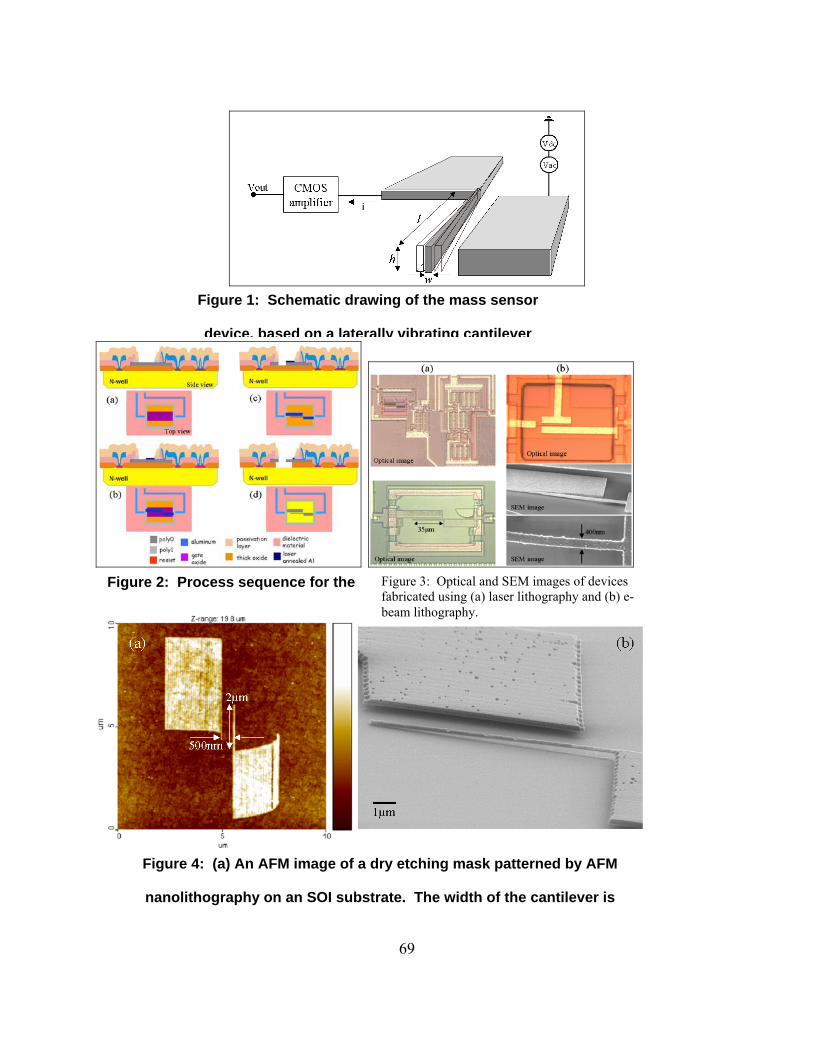
69
Figure 1: Schematic drawing of the mass sensor
device, based on a laterally vibrating cantilever
Figure 3: Optical and SEM images of devices fabricated using (a) laser lithography and (b) e-beam lithography.
Figure 2: Process sequence for the
Figure 4: (a) An AFM image of a dry etching mask patterned by AFM
nanolithography on an SOI substrate. The width of the cantilever is
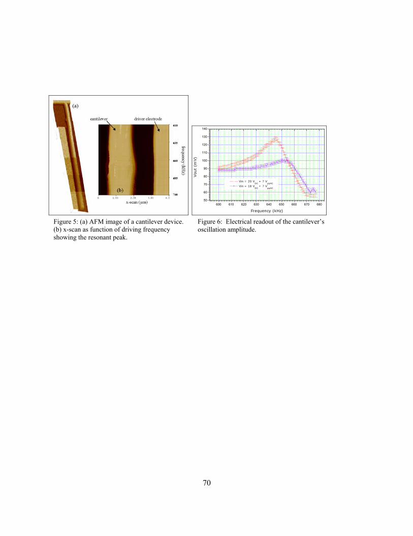
600 610 620 630 640 650 660 670 680
50
60
70
80
90
100
110
120
130
140
Vin = 20 VDC
+ 7 VppAC
Vin = 18 VDC
+ 7 VppAC
Vout
(mV)
Frequency (kHz) Figure 6: Electrical readout of the cantilever’s oscillation amplitude.
Figure 5: (a) AFM image of a cantilever device. (b) x-scan as function of driving frequency showing the resonant peak.
70
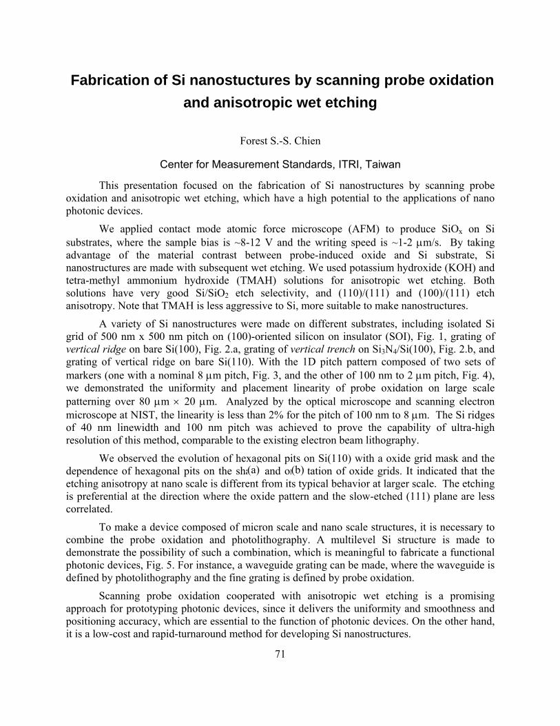
Fabrication of Si nanostuctures by scanning probe oxidation and anisotropic wet etching
Forest S.-S. Chien
Center for Measurement Standards, ITRI, Taiwan
This presentation focused on the fabrication of Si nanostructures by scanning probe oxidation and anisotropic wet etching, which have a high potential to the applications of nano photonic devices.
We applied contact mode atomic force microscope (AFM) to produce SiOx on Si substrates, where the sample bias is ~8-12 V and the writing speed is ~1-2 μm/s. By taking advantage of the material contrast between probe-induced oxide and Si substrate, Si nanostructures are made with subsequent wet etching. We used potassium hydroxide (KOH) and tetra-methyl ammonium hydroxide (TMAH) solutions for anisotropic wet etching. Both solutions have very good Si/SiO2 etch selectivity, and (110)/(111) and (100)/(111) etch anisotropy. Note that TMAH is less aggressive to Si, more suitable to make nanostructures.
A variety of Si nanostructures were made on different substrates, including isolated Si grid of 500 nm x 500 nm pitch on (100)-oriented silicon on insulator (SOI), Fig. 1, grating of vertical ridge on bare Si(100), Fig. 2.a, grating of vertical trench on Si3N4/Si(100), Fig. 2.b, and grating of vertical ridge on bare Si(110). With the 1D pitch pattern composed of two sets of markers (one with a nominal 8 μm pitch, Fig. 3, and the other of 100 nm to 2 μm pitch, Fig. 4), we demonstrated the uniformity and placement linearity of probe oxidation on large scale patterning over 80 μm × 20 μm. Analyzed by the optical microscope and scanning electron microscope at NIST, the linearity is less than 2% for the pitch of 100 nm to 8 μm. The Si ridges of 40 nm linewidth and 100 nm pitch was achieved to prove the capability of ultra-high resolution of this method, comparable to the existing electron beam lithography.
We observed the evolution of hexagonal pits on Si(110) with a oxide grid mask and the dependence of hexagonal pits on the shape and orientation of oxide grids. It indicated that the etching anisotropy at nano scale is different from its typical behavior at larger scale. The etching is preferential at the direction where the oxide pattern and the slow-etched (111) plane are less correlated.
(a) (b)
To make a device composed of micron scale and nano scale structures, it is necessary to combine the probe oxidation and photolithography. A multilevel Si structure is made to demonstrate the possibility of such a combination, which is meaningful to fabricate a functional photonic devices, Fig. 5. For instance, a waveguide grating can be made, where the waveguide is defined by photolithography and the fine grating is defined by probe oxidation.
Scanning probe oxidation cooperated with anisotropic wet etching is a promising approach for prototyping photonic devices, since it delivers the uniformity and smoothness and positioning accuracy, which are essential to the function of photonic devices. On the other hand, it is a low-cost and rapid-turnaround method for developing Si nanostructures.
71
240 nm
150 nm
Fig. 2. (a) vertical ridge on
Si(100) and (b) vertical trench on
Si3N4/Si(100).
500 nm
500
nm
Fig. 1. Si grid on SOI.
Fig. 3. Markers of a nominal 8 μm pitch.
80 μm
20 μm8 μm
Fig. 4. Fine markers.
1 μm
Fig. 5. Multilevel structures
72
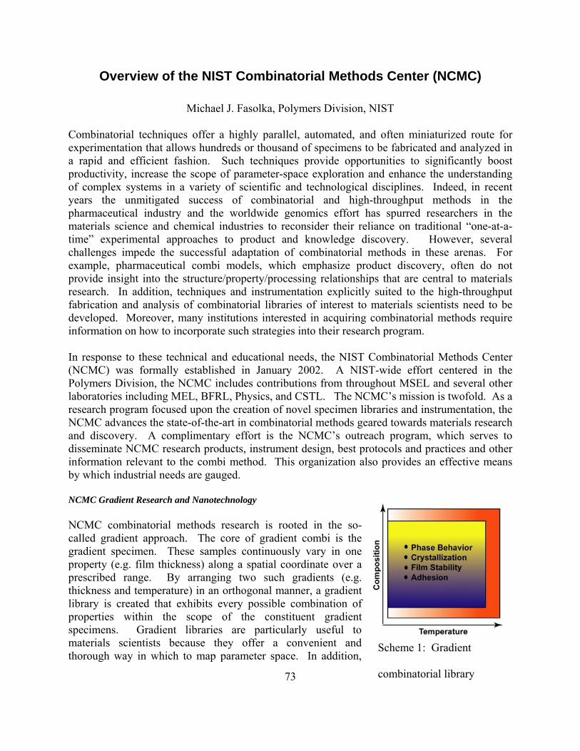
Overview of the NIST Combinatorial Methods Center (NCMC)
Michael J. Fasolka, Polymers Division, NIST Combinatorial techniques offer a highly parallel, automated, and often miniaturized route for experimentation that allows hundreds or thousand of specimens to be fabricated and analyzed in a rapid and efficient fashion. Such techniques provide opportunities to significantly boost productivity, increase the scope of parameter-space exploration and enhance the understanding of complex systems in a variety of scientific and technological disciplines. Indeed, in recent years the unmitigated success of combinatorial and high-throughput methods in the pharmaceutical industry and the worldwide genomics effort has spurred researchers in the materials science and chemical industries to reconsider their reliance on traditional “one-at-a-time” experimental approaches to product and knowledge discovery. However, several challenges impede the successful adaptation of combinatorial methods in these arenas. For example, pharmaceutical combi models, which emphasize product discovery, often do not provide insight into the structure/property/processing relationships that are central to materials research. In addition, techniques and instrumentation explicitly suited to the high-throughput fabrication and analysis of combinatorial libraries of interest to materials scientists need to be developed. Moreover, many institutions interested in acquiring combinatorial methods require information on how to incorporate such strategies into their research program. In response to these technical and educational needs, the NIST Combinatorial Methods Center (NCMC) was formally established in January 2002. A NIST-wide effort centered in the Polymers Division, the NCMC includes contributions from throughout MSEL and several other laboratories including MEL, BFRL, Physics, and CSTL. The NCMC’s mission is twofold. As a research program focused upon the creation of novel specimen libraries and instrumentation, the NCMC advances the state-of-the-art in combinatorial methods geared towards materials research and discovery. A complimentary effort is the NCMC’s outreach program, which serves to disseminate NCMC research products, instrument design, best protocols and practices and other information relevant to the combi method. This organization also provides an effective means by which industrial needs are gauged. NCMC Gradient Research and Nanotechnology NCMC combinatorial methods research is rooted in the so-called gradient approach. The core of gradient combi is the gradient specimen. These samples continuously vary in one property (e.g. film thickness) along a spatial coordinate over a prescribed range. By arranging two such gradients (e.g. thickness and temperature) in an orthogonal manner, a gradient library is created that exhibits every possible combination of properties within the scope of the constituent gradient specimens. Gradient libraries are particularly useful to materials scientists because they offer a convenient and thorough way in which to map parameter space. In addition,
Scheme 1: Gradient
combinatorial library 73
74
gradient libraries are especially amenable to examination via microscopy and micro-analysis, which facilitates the illumination of structure-property relationships. Finally, as opposed to many robotics-oriented discrete approaches, gradient techniques can offer a cost effective way of performing combinatorial studies, making them attractive to a wider range of institutions.
As they are the basic unit of gradient libraries, many NCMC research efforts concentrate upon the development of novel gradient specimens and processes, with polymer science being a focus in recent years. NCMC methods for producing gradients in film thickness (20 nm to 250 nm range), composition (dilute solutions, including nanoparticles) and temperature (-5 °C to 250 °C) provide a foundation for combinatorial studies of materials properties and processing. This year, several new techniques were added to the NCMC repertoire. New instrumentation for generating gradients in UV-radiation exposure was central to this effort. Here, a UV slit-source is accelerated across a planar specimen. When this source is held in close proximity (< 5 mm) to the sample UV-generated ozone can chemically modify SAM treated sample surfaces, resulting in a gradient in surface energy and/or chemical functionality. Depending upon the SAM employed, such surface energy gradients can span 70° in water contact angle (20 J/m2 to 78 J/m2). Larger source/sample distances are effective in producing gradients in light-induced crosslinking, polymerization and degradation. Since the degree of UV exposure is controlled through stage motion, this instrument is particularly versatile. Gradient profile, depth and steepness are easily tuned for a wide range of applications. One of these is a gradient specimen useful for gauging the chemical sensitivity of Chemical Force Microscopy (CFM). Here, a hydrophobic SAM is microcontact printed onto the substrate to form mm-scale lines. Subsequent filling with a hydrophilic SAM results in a chemically heterogeneous surface. When a gradient in UV exposure is applied to this specimen, the chemical contrast between the hydrophilic and hydrophobic domains is reduced along the gradient direction, i.e. the hydrophobic SAM is gradually converted into hydrophilic species. Performing CFM along this gradient, which can be calibrated with spectroscopic techniques or water contact angle, gives a measure of the probe sensitivity and a more quantitative aspect to CFM images.
In another new technique, gradients in the height of topographic surface features can be created. Here, topographic gratings are lithographically etched into wedges of silsesquioxane “spin-on” oxides created via flow-coating. The resulting patterns, with heights ranging from 30 nm to 150 nm, provide a combi strategy for examining topography-mediated templating of film properties, for example the self-assembly of block copolymers and photonic colloids.
Given their scope, many NCMC techniques are well geared to advance nanotechnology, MEMS and other thin next-generation devices. In order to best harness these techniques for higher-tech aims, during the past year, the NCMC has been collaborating with MEL to produce a host of tools, including lithographic masks and imprinting approaches, that combine the precision and manufacturing expertise found in MEL with the combi- approach to experimentation. For more information about the NIST Combinatorial Methods Center, including a list of NCMC publications relevant to this article, please visit our web site at http://www.nist.gov/combi.
75
Nanolithography and Microfluidics: A Manufacturing Perspective
T.L. Schmitz1, J.A. Dagata2 , B. Dutterer2
1Department of Mechanical and Aerospace Engineering, University of Florida, Gainesville, FL, USA
2National Institute of Standards and Technology, Gaithersburg, MD, USA
Abstract Microfluidic systems for analytical, medical, and sensing applications integrate optical or electrical readouts in low-cost, low-volume consumption systems. Embedding chemically functionalized templates with nanoscale topography within these devices links the scale at which molecular recognition and self-organization occurs and the macroscopic layout of fluid channels, mixing volumes, and detection regions. This paper addresses a path toward standardization of manufacturing procedures for microfluidic devices through: 1) scanning probe lithography to produce sub-50-nm scale features in a silicon master; 2) master replication in plastics by hot embossing; and 3) the development of a generic microfluidic experimental platform that orients 125 micrometer channels embossed in a poly(vinyl chloride) gasket to an array of high-speed machined channels and a silicon substrate.
Introduction
The use of microfluidic systems in biological, analytical, medical, and sensing applications is continually growing. Applications include, for example, studies of synergistic/antagonistic interactions between two drug substances and DNA analysis. To this point, many research efforts have focused on the ability to either produce sub-micrometer scale features or replicate these features in polymers [e.g., 1-7]. However, the manufacture of the platforms where the microfluidic experiments are completed and results evaluated has remained primarily a benchtop activity with little thought given to standardization. In this paper, we describe initial efforts in the development of a suite of manufacturing procedures for the production and rapid replication of microfluidic testing platforms. These manufacturing methods include 1) scanning probe lithography to produce sub-50-nm scale features on a standard sized silicon master; 2) hot embossing for replication of the silicon master, or other larger-scale features (≥100 μm), in polymers; and 3) high-speed machining for the production of the microfluidic experimental platform, as well as any hot embossing tooling required for larger-scale features.
MANUFACTURING METHODS
Prior to providing a description of the standardized microfluidic experimental platform, we present an overview of the production methods applied in this research. However, it is expected that other capabilities will be added in the future.
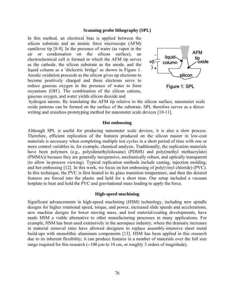
Scanning probe lithography (SPL)
In this method, an electrical bias is applied between the silicon substrate and an atomic force microscope (AFM) cantilever tip [8-9]. In the presence of water (as vapor in the air or condensation on the silicon surface), an electrochemical cell is formed in which the AFM tip serves as the cathode, the silicon substrate as the anode, and the liquid column as a ‘dielectric bridge’ as shown in Figure 1. Anodic oxidation proceeds as the silicon gives up electrons to become positively charged and these electrons serve to reduce gaseous oxygen in the presence of water to form oxyanions (OH-). The combination of the silicon cations, gaseous oxygen, and water yields silicon dioxide and
AFM tip
silicon
oxideliquid
columnv(t) +
-
Figure 1: SPL
AFM tip
silicon
oxideliquid
columnv(t) +
-
Figure 1: SPL
hydrogen anions. By translating the AFM tip relative to the silicon surface, nanometer scale oxide patterns can be formed on the surface of the substrate. SPL therefore serves as a direct-writing and resistless prototyping method for nanometer scale devices [10-11].
Hot embossing
Although SPL is useful for producing nanometer scale devices, it is also a slow process. Therefore, efficient replication of the features produced on the silicon master in low-cost materials is necessary when completing multiple test cycles in a short period of time with one or more control variables in, for example, chemical analysis. Traditionally, the replication materials have been polymers (e.g., poly(dimethylsiloxane) (PDMS) and poly(methyl methacrylate) (PMMA)) because they are generally inexpensive, mechanically robust, and optically transparent (to allow in-process viewing). Typical replication methods include casting, injection molding, and hot embossing [12]. In this work, we focus on hot embossing of poly(vinyl chloride) (PVC). In this technique, the PVC is first heated to its glass transition temperature, and then the desired features are forced into the plastic and held for a short time. Our setup included a vacuum hotplate to heat and hold the PVC and gravitational mass loading to apply the force.
High-speed machining
Significant advancements in high-speed machining (HSM) technology, including new spindle designs for higher rotational speed, torque, and power, increased slide speeds and accelerations, new machine designs for lower moving mass, and tool material/coating developments, have made HSM a viable alternative to other manufacturing processes in many applications. For example, HSM has been used extensively in the aerospace industry, where the dramatic increases in material removal rates have allowed designers to replace assembly-intensive sheet metal build-ups with monolithic aluminum components [13]. HSM has been applied in this research due to its inherent flexibility; it can produce features in a number of materials over the full size range required for this research (∼100 μm to 10 cm, or roughly 3 orders of magnitude).
76
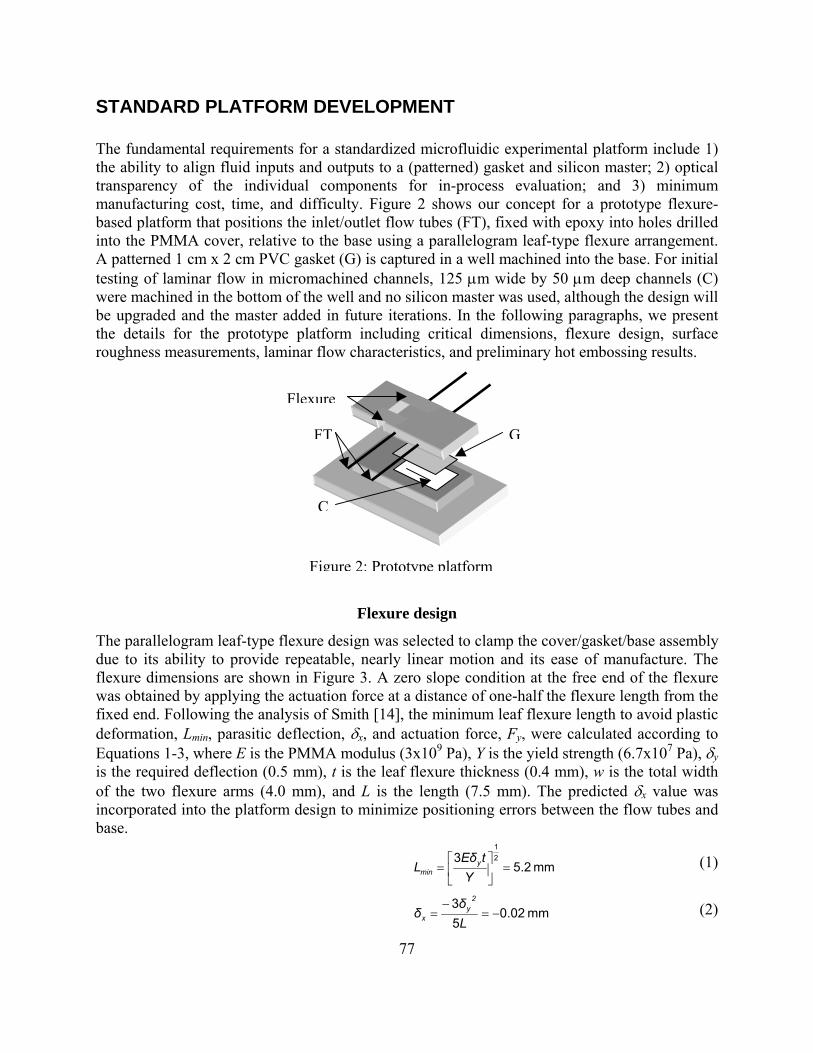
STANDARD PLATFORM DEVELOPMENT The fundamental requirements for a standardized microfluidic experimental platform include 1) the ability to align fluid inputs and outputs to a (patterned) gasket and silicon master; 2) optical transparency of the individual components for in-process evaluation; and 3) minimum manufacturing cost, time, and difficulty. Figure 2 shows our concept for a prototype flexure-based platform that positions the inlet/outlet flow tubes (FT), fixed with epoxy into holes drilled into the PMMA cover, relative to the base using a parallelogram leaf-type flexure arrangement. A patterned 1 cm x 2 cm PVC gasket (G) is captured in a well machined into the base. For initial testing of laminar flow in micromachined channels, 125 μm wide by 50 μm deep channels (C) were machined in the bottom of the well and no silicon master was used, although the design will be upgraded and the master added in future iterations. In the following paragraphs, we present the details for the prototype platform including critical dimensions, flexure design, surface roughness measurements, laminar flow characteristics, and preliminary hot embossing results.
Flexure
FT G
C
Figure 2: Prototype platform
Flexure design
The parallelogram leaf-type flexure design was selected to clamp the cover/gasket/base assembly due to its ability to provide repeatable, nearly linear motion and its ease of manufacture. The flexure dimensions are shown in Figure 3. A zero slope condition at the free end of the flexure was obtained by applying the actuation force at a distance of one-half the flexure length from the fixed end. Following the analysis of Smith [14], the minimum leaf flexure length to avoid plastic deformation, Lmin, parasitic deflection, δx, and actuation force, Fy, were calculated according to Equations 1-3, where E is the PMMA modulus (3x10⁹ Pa), Y is the yield strength (6.7x10⁷ Pa), δy is the required deflection (0.5 mm), t is the leaf flexure thickness (0.4 mm), w is the total width of the two flexure arms (4.0 mm), and L is the length (7.5 mm). The predicted δx value was incorporated into the platform design to minimize positioning errors between the flow tubes and base.
mm5.23 2
1
Y
tEδL y
min =⎥⎦
⎤⎢⎣
⎡= (1)
mm0.0253
Lδ
δ2
yx −=
−= (2)
77
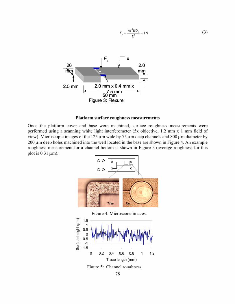
N 1== 3y
3
y LEδwt
F (3)
2.0 mm
2.0 mm x 0.4 mm x 7.5 mm
Fy
20 mm
50 mm
2.5 mm
Figure 3: Flexure
xy 2.0
mm
2.0 mm x 0.4 mm x 7.5 mm
Fy
20 mm
50 mm
2.5 mm
Figure 3: Flexure
xy
Platform surface roughness measurements
Once the platform cover and base were machined, surface roughness measurements were performed using a scanning white light interferometer (5x objective, 1.2 mm x 1 mm field of view). Microscopic images of the 125 μm wide by 75 μm deep channels and 800 μm diameter by 200 μm deep holes machined into the well located in the base are shown in Figure 4. An example roughness measurement for a channel bottom is shown in Figure 5 (average roughness for this plot is 0.31 μm).
-1.5-1
-0.50
0.51
1.5
0 0.2 0.4 0.6 0.8 1 1.2Trace length (mm)
Surfa
ce h
eigh
t (μm
)
Figure 5: Channel roughness
20x 5x
Figure 4: Microscope images.
78
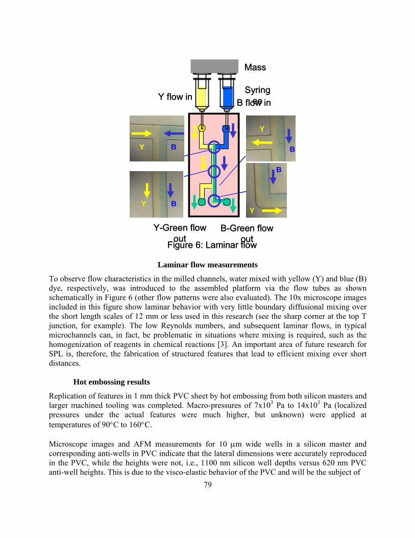
79
outB-Green flow
out
Y flow in B flow in
Y-Green flow
Laminar flow measurements
To observe flow characteristics in the milled channels, water mixed with yellow (Y) and blue (B) dye, respectively, was introduced to the assembled platform via the flow tubes as shown schematically in Figure 6 (other flow patterns were also evaluated). The 10x microscope images included in this figure show laminar behavior with very little boundary diffusional mixing over the short length scales of 12 mm or less used in this research (see the sharp corner at the top T junction, for example). The low Reynolds numbers, and subsequent laminar flows, in typical microchannels can, in fact, be problematic in situations where mixing is required, such as the homogenization of reagents in chemical reactions [3]. An important area of future research for SPL is, therefore, the fabrication of structured features that lead to efficient mixing over short distances.
Hot embossing results
Replication of features in 1 mm thick PVC sheet by hot embossing from both silicon masters and larger machined tooling was completed. Macro-pressures of 7x10³ Pa to 14x103 Pa (localized pressures under the actual features were much higher, but unknown) were applied at temperatures of 90°C to 160°C. Microscope images and AFM measurements for 10 μm wide wells in a silicon master and corresponding anti-wells in PVC indicate that the lateral dimensions were accurately reproduced in the PVC, while the heights were not, i.e., 1100 nm silicon well depths versus 620 nm PVC anti-well heights. This is due to the visco-elastic behavior of the PVC and will be the subject of
Y B
Y B
B
Y
B
Y
Mass
Syringee
Figure 6: Laminar flow
Y flow in B flow in
Y-Green flow out
B-Green flow out
Y
Y B
Y B
B
B
Y
Mass
Syringee
Figure 6: Laminar flow
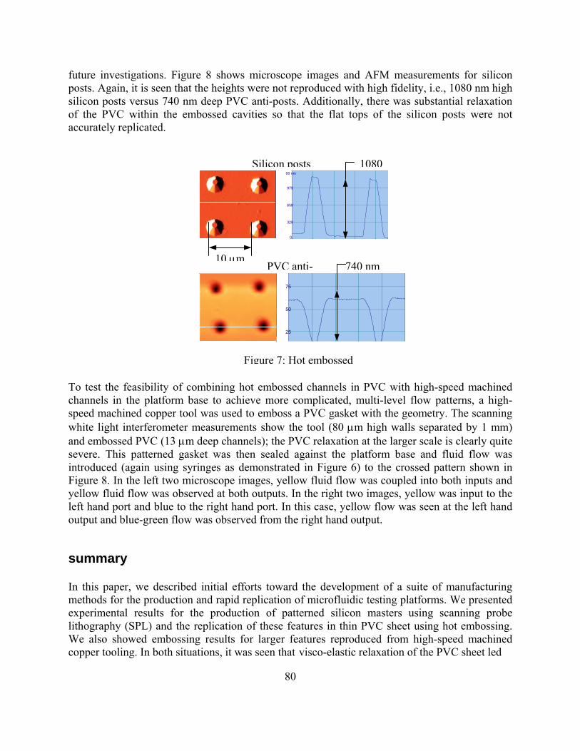
future investigations. Figure 8 shows microscope images and AFM measurements for silicon posts. Again, it is seen that the heights were not reproduced with high fidelity, i.e., 1080 nm high silicon posts versus 740 nm deep PVC anti-posts. Additionally, there was substantial relaxation of the PVC within the embossed cavities so that the flat tops of the silicon posts were not accurately replicated.
Distance (µm)
0
325
650
975
00 nm
0 2.66 5.32 7.98 10.64 1
1080
10 μm
Silicon posts
0
25
50
75
0 2 68 5 36 8 04 10 72 13 4
PVC anti- 740 nm
Figure 7: Hot embossed To test the feasibility of combining hot embossed channels in PVC with high-speed machined channels in the platform base to achieve more complicated, multi-level flow patterns, a high-speed machined copper tool was used to emboss a PVC gasket with the geometry. The scanning white light interferometer measurements show the tool (80 μm high walls separated by 1 mm) and embossed PVC (13 μm deep channels); the PVC relaxation at the larger scale is clearly quite severe. This patterned gasket was then sealed against the platform base and fluid flow was introduced (again using syringes as demonstrated in Figure 6) to the crossed pattern shown in Figure 8. In the left two microscope images, yellow fluid flow was coupled into both inputs and yellow fluid flow was observed at both outputs. In the right two images, yellow was input to the left hand port and blue to the right hand port. In this case, yellow flow was seen at the left hand output and blue-green flow was observed from the right hand output.
summary
In this paper, we described initial efforts toward the development of a suite of manufacturing methods for the production and rapid replication of microfluidic testing platforms. We presented experimental results for the production of patterned silicon masters using scanning probe lithography (SPL) and the replication of these features in thin PVC sheet using hot embossing. We also showed embossing results for larger features reproduced from high-speed machined copper tooling. In both situations, it was seen that visco-elastic relaxation of the PVC sheet led
80
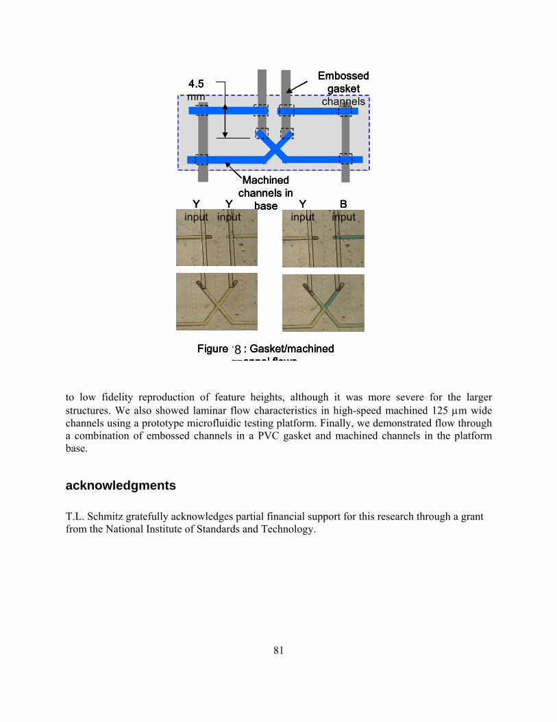
Embossed gasket
channels4.5 mm
Machined channels in
baseY input
Y input
Y input
B input
Figure 10: Gasket/machined channel flows
Embossed gasket
channels4.5 mm
Machined channels in
baseY input
Y input
Y input
B input
Figure 10: Gasket/machined channel flows8
Embossed gasket
channels4.5 mm
Machined channels in
baseY input
Y input
Y input
B input
Figure 10: Gasket/machined channel flows
Embossed gasket
channels4.5 mm
Machined channels in
baseY input
Y input
Y input
B input
Figure 10: Gasket/machined channel flows8
to low fidelity reproduction of feature heights, although it was more severe for the larger structures. We also showed laminar flow characteristics in high-speed machined 125 μm wide channels using a prototype microfluidic testing platform. Finally, we demonstrated flow through a combination of embossed channels in a PVC gasket and machined channels in the platform base.
acknowledgments
T.L. Schmitz gratefully acknowledges partial financial support for this research through a grant from the National Institute of Standards and Technology.
81
82
references
[1] Dasgupta, P., Surowiec, K., Berg, J., 2002, Flow of Multiple Fluids in a Small Dimension, Analytical Chemistry, 74/7: 208A-213A.
[2] McDonald, J., Chabinyc, M., Metallo, S., Anderson, J., Stroock, A., Whitesides, G., 2002, Prototyping of Microfluidic Devices in Poly(dimethylsiloxane) Using Solid-Object Printing, Analytical Chemistry, 74/7: 1537-1545.
[3] Stroock, A., Dertinger, S., Ajdari, A., Mezić, I., Stone, H., Whitesides, G., 2002, Chaotic Mixer for Microchannels, Science, 295: 647-651.
[4] Tamanaha, C., Whitman, L., Colton, R., 2002, Hybrid Macro-micro Fluidics System for a Chip-based Biosensor, Journal of Micromechanics and Microengineering, 12: N7-N17.
[5] Lin, L., Cheng, Y.T., Chiu, C.J., 1998, Comparative Study of Hot Embossed Micro Structures Fabricated by Laboratory and Commercial Environments, Microsystem Technologies, 4: 113-116.
[6] Tan, H., Gilbertson, A., Chou, S., 1998, Roller Nanoimprint Lithography, Journal of Vacuum Science and Technology B, 16/6: 3926-3928.
[7] Stix, G., 2002, Soft Manufacturing, Scientific American, 287/2: 30-31. [8] Chien, F.S., Hsieh, W.F., Gwo, S., Vladar, A.E., Dagata, J.A., 2002, Silicon Nanostructures Fabricated by
Scanning Probe Oxidation and Tetra-methyl Ammonium Hydroxide Etching, Journal of Applied Physics, 91: 10044.
[9] Matsumoto, K., Gotoh, Y., Maeda, T., Dagata, J.A., Harris, J., 2000, Room-temperature Single-electron Memory Made by Pulse-Mode Atomic Force Microscopy Nano Oxidation Process on Atomically Flat α-Alumina Substrate, Applied Physics Letters, 76/2: 239-241.
[10] Dagata, J.A., 1995, Device Fabrication by Scanned Probe Oxidation, Science, 270: 1625-1626. [11] Dagata, J.A., Schneir, J., Harary, H.H., Evans, C.J., Postek, M.T., Bennett, J., 1990, Modification of Hydrogen-
Passivated Silicon by a Scanning Tunneling Microscope Operating in Air, Applied Physics Letters, 56: 2001-2003.
[12] Gale, M.T., 1997, Replication, in Micro-optics, Elements, Systems, and Applications, H.P. Herzig, Ed., Taylor and Francis, London.
[13] Halley, J., Helvey, A., Smith, K.S., Winfough, W.R., 1999, The Impact of High-Speed Machining on the Design and Fabrication of Aircraft Components, Proceedings of the 17th Biennial Conference on Mechanical Vibration and Noise, 1999 ASME Design and Technical Conferences, September 12-16, Las Vegas, Nevada.
[14] Smith, S.T., 2000, Flexures, Gordon and Breach Science Publishers, London.

83
PARTICIPANTS LIST

84
85
PARTICIPANTS LIST Francesc Perez-Murano Institut de Microelectronica de Barcelona (IMB) Centro Nacional Microelectrónica (CNM) Campus Universitat Autonoma de Barcelona E-08193 Bellaterra. SPAIN Phone: (34)93 594 77 00 (ext. 1206, 1054) Fax: (34) 93 580 14 96 e-mail: [email protected] Zachary Davis Mikroelektronik Centret Technical University of Denmark, Bldg. 345e Dk-2800 Lyngby, Denmark Tel. direct: +45 4525 5733 Fax: +45 4588 7762 e-mail: [email protected] Hiroshi Yokoyama Nanotechnology Research Institute National Institute of Advanced Industrial Science and Technology (AIST) 1-1-1 Umezono, Tsukuba, Ibaraki 305-8568, Japan Phone: +81-298-61-5538, FAX: +81-298-61-5548 E-mail: [email protected] Kuramochi Hiromi Nanotechnology Research Institute National Institute of Advanced Industrial Science and Technology Research Consortium for Synthetic Nano-Function Materials Project Tsukuba Central 4, 1-1-1 Higashi, Tsukuba, Ibaraki 305-8562, Japan TEL: +81-(0)298-61-5080 ex.55014 FAX: +81-(0)298-61-2786 Email: [email protected] Dr. Takashi TOKIZAKI Near-Field Nano-Engineering Group Nanotechnology Research Institute National Institute of Advanced Industrial Science and Technology AIST Tsukuba Central 2, Tsukuba, Ibaraki 305-8568, JAPAN Phone: +81-298-61-5395 Fax: +81-298-61-5400 e-mail: [email protected]
Forest Chien Center for Measurement Standards Industrial Technology Research Institute E200 Bldg 16 321 Kuang Fu Rd Sec 2 Hsinchu Taiwan 300 TEL: 886-3-5743730 FAX: 886-3-5724952 Email: [email protected] Shangjr Gwo, Department of Physics National Tsing-Hua University Hsinchu 300, Taiwan 886-3-5742636 886-3-5723052 [email protected] Gerald W. Young Department of Mathematics & Computer Science Ayer Hall 230 University of Akron Akron OH 44325-4002 330-972-5731 tel 330-374-8630 fax [email protected] Rex D. Ramsier Departments of Physics, Chemistry, and Chemical Engineering Ayer Hall Room 111 250 Buchtel Commons The University of Akron Akron, OH 44325-4001 USA ph: 330-972-4936 fax: 330-972-6918 e-mail: [email protected] Tony Schmitz University of Florida Department of Mechanical and Aerospace Engineering 237 MEB Gainesville, FL 32611 Phone: (352) 392-8909 Fax: (352) 392-1071 Email: [email protected]

86
John A. Dagata Precision Engineering Division Manufacturing Engineering Laboratory National Institute of Standards and Technology 100 Bureau Drive Stop (8212) Gaithersburg MD 20899-8212 Phone: 301-975-3597 Email: [email protected] Michael Fasolka NIST Combinatorial Methods Center Polymers Division (854) National Institute of Standards and Technology 100 Bureau Drive, Stop 8542 Gaithersburg MD 20899-8212 Phone: 301-975-8526 Email: [email protected] Joseph Fu Precision Engineering Division Manufacturing Engineering Laboratory National Institute of Standards and Technology 100 Bureau Drive Stop (8212) Gaithersburg MD 20899-8212 Phone: 301-975-3495 Email: [email protected] Dale Hall, Director Manufacturing Engineering Laboratory National Institute of Standards and Technology 100 Bureau Drive Stop (8200) Gaithersburg MD 20899-8200 Phone: 301-975-3400 Email: [email protected] John Kramar Precision Engineering Division Manufacturing Engineering Laboratory National Institute of Standards and Technology 100 Bureau Drive Stop (8212) Gaithersburg MD 20899-8212 Phone: 301-975-3447 Email: [email protected] Kevin Lyons Manufacturing Systems Integration Division Manufacturing Engineering Laboratory National Institute of Standards and Technology 100 Bureau Drive Stop (8263) Gaithersburg MD 20899-8263 Phone: 301-975-6550 Email: [email protected]
Michael Postek Nanoscale Metrology Group Precision Engineering Division Manufacturing Engineering Laboratory National Institute of Standards and Technology 100 Bureau Drive Stop (8212) Gaithersburg MD 20899-8212 Phone: 301-975-2299 Email: [email protected] Richard Silver Precision Engineering Division Manufacturing Engineering Laboratory National Institute of Standards and Technology 100 Bureau Drive Stop (8212) Gaithersburg MD 20899-8212 Phone: 301-975-5609 Email: [email protected] John Suehle Semiconductor Electronics Division Electrical and Electronics Engineering Laboratory National Institute of Standards and Technology 100 Bureau Drive Stop (812) Gaithersburg MD 20899-812 Phone: 301-975-2247 Email: [email protected] Dennis Swyt, Chief Precision Engineering Division Manufacturing Engineering Laboratory National Institute of Standards and Technology 100 Bureau Drive Stop (8210) Gaithersburg MD 20899-8210 Phone: 301-975-3463 Email: [email protected] Xianfan Xu, Associate Professor School of Mechanical Engineering Purdue University West Lafayette, IN 47907 Phone: (765) 494-5639 Fax: (765) 494-0539 URL: http://widget.ecn.purdue.edu/~xxu Clayton Teague, Chief Manufacturing Metrology Division Manufacturing Engineering Laboratory National Institute of Standards and Technology 100 Bureau Drive Stop (8220) Gaithersburg MD 20899-8220 Phone: 301-975-6600 Email: [email protected]