Embed Size (px)
Citation preview

ORISE Technology reserves the right to change this documentation without prior notice. Information provided by ORISE Technology is believed to be accurate and reliable. However, ORISE Technology makes no warranty for any errors which may appear in this document. Contact ORISE Technology to obtain the latest version of device specifications before placing your order. No responsibility is assumed by ORISE Technology for any infringement of patent or other rights of third parties which may result from its use. In addition, ORISE products are not authorized for use as critical components in life support devices/ systems or aviation devices/systems, where a malfunction or failure of the product may reasonably be expected to result in significant injury to the user, without the express written approval of ORISE.
MAR. 30, 2007
Version 1.0
SSPPLLCC550022BB113322 xx 6655 DDoott MMaattrriixx LLCCDD DDrriivveerr

SPLC502B
© ORISE Technology Co., Ltd. Proprietary & Confidential
2 MAR. 30, 2007Version: 1.0
Table of Contents PAGE
1. GENERAL DESCRIPTION .......................................................................................................................................................................... 4 2. FEATURES.................................................................................................................................................................................................. 4 3. ORDERING INFORMATION........................................................................................................................................................................ 5 4. BLOCK DIAGRAM ...................................................................................................................................................................................... 5 5. SIGNAL DESCRIPTIONS............................................................................................................................................................................ 6
5.1. POWER SUPPLY PINS .......................................................................................................................................................................... 6 5.2. LCD POWER SUPPLY CIRCUIT TERMINALS ........................................................................................................................................... 6 5.3. SYSTEM BUS CONNECTION TERMINALS................................................................................................................................................ 7 5.4. LIQUID CRYSTAL DRIVE TERMINALS...................................................................................................................................................... 9 5.5. TEST TERMINALS ................................................................................................................................................................................ 9
6. FUNCTIONAL DESCRIPTIONS................................................................................................................................................................ 10 6.1. THE MPU INTERFACE........................................................................................................................................................................ 10 6.2. THE CHIP SELECT ..............................................................................................................................................................................11 6.3. ACCESSING THE DISPLAY DATA RAM AND THE INTERNAL REGISTERS ...................................................................................................11 6.4. THE BUSY FLAG.................................................................................................................................................................................11 6.5. DISPLAY DATA RAM .......................................................................................................................................................................... 12 6.6. THE DISPLAY DATA LATCH CIRCUIT .................................................................................................................................................... 14 6.7. THE OSCILLATOR CIRCUIT ................................................................................................................................................................. 14 6.8. THE COMMON OUTPUT STATUS SELECT............................................................................................................................................. 14 6.9. DISPLAY TIMING GENERATOR CIRCUIT ............................................................................................................................................... 14 6.10. THE LIQUID CRYSTAL DRIVER CIRCUITS ............................................................................................................................................. 16 6.10. THE LIQUID CRYSTAL DRIVER CIRCUITS ............................................................................................................................................. 16 6.11. THE POWER SUPPLY CIRCUITS .......................................................................................................................................................... 17 6.12. HIGH POWER MODE.......................................................................................................................................................................... 20 6.13. THE INTERNAL POWER SUPPLY SHUTDOWN COMMAND SEQUENCE..................................................................................................... 20 6.14. REFERENCE CIRCUIT EXAMPLES ....................................................................................................................................................... 21 6.15. THE RESET CIRCUIT.......................................................................................................................................................................... 23
7. COMMANDS ............................................................................................................................................................................................. 23 7.1. DISPLAY ON/OFF ............................................................................................................................................................................. 24 7.2. DISPLAY START LINE SET .................................................................................................................................................................. 24 7.3. PAGE ADDRESS SET.......................................................................................................................................................................... 24 7.4. COLUMN ADDRESS SET..................................................................................................................................................................... 25 7.5. STATUS READ ................................................................................................................................................................................... 25 7.6. DISPLAY DATA WRITE ........................................................................................................................................................................ 26 7.7. DISPLAY DATA READ.......................................................................................................................................................................... 26 7.8. ADC SELECT (SEGMENT DRIVER DIRECTION SELECT) ....................................................................................................................... 26 7.9. DISPLAY NORMAL/REVERSE .............................................................................................................................................................. 26 7.10. DISPLAY ALL POINTS ON/OFF........................................................................................................................................................... 27 7.11. LCD BIAS SET .................................................................................................................................................................................. 27 7.12. READ/MODIFY/WRITE........................................................................................................................................................................ 27 7.13. END................................................................................................................................................................................................. 28 7.14. RESET ............................................................................................................................................................................................ 29

SPLC502B
© ORISE Technology Co., Ltd. Proprietary & Confidential
3 MAR. 30, 2007Version: 1.0
7.15. COMMON OUTPUT MODE SELECT ...................................................................................................................................................... 29 7.16. POWER CONTROLLER SET ................................................................................................................................................................ 29 7.17. V0 VOLTAGE REGULATOR INTERNAL RESISTOR RATIO SET ................................................................................................................. 30 7.18. THE ELECTRONIC VOLUME (DOUBLE BYTE COMMAND)....................................................................................................................... 30 7.19. STATIC INDICATOR (DOUBLE BYTE COMMAND).................................................................................................................................... 31 7.20. PAGE BLINKING (DOUBLE BYTE COMMAND)........................................................................................................................................ 31 7.21. SET DRIVING MODE (DOUBLE BYTE COMMAND) ................................................................................................................................. 32 7.22. POWER SAVE (COMPOUND COMMAND) .............................................................................................................................................. 33 7.23. NOP ................................................................................................................................................................................................ 34 7.24. TEST............................................................................................................................................................................................... 34 7.25. OSCILLATOR FREQUENCY SELECTION ................................................................................................................................................ 34 7.26. TABLE 13 TABLE OF SPLC502B COMMANDS...................................................................................................................................... 35
8. COMMAND DESCRIPTION ...................................................................................................................................................................... 37 8.1. INSTRUCTION SETUP: REFERENCE (REFERENCE)............................................................................................................................... 37
9. ELECTRICAL SPECIFICATIONS ............................................................................................................................................................. 39 9.1. ABSOLUTE MAXIMUM RATINGS .......................................................................................................................................................... 39 9.2. DC CHARACTERISTICS ...................................................................................................................................................................... 39 9.3. DISPLAY PATTERN CHECKER.............................................................................................................................................................. 40 9.4. DISPLAY PATTERN CHECKER.............................................................................................................................................................. 40 9.5. TIMING CHARACTERISTICS................................................................................................................................................................. 42 9.6. THE MPU INTERFACE (REFERENCE EXAMPLES)................................................................................................................................. 48 9.7. CONNECTIONS BETWEEN LCD DRIVERS (REFERENCE EXAMPLE)........................................................................................................ 50 9.8. CONNECTIONS BETWEEN LCD DRIVERS (REFERENCE EXAMPLES)...................................................................................................... 51
10. VLCD VOLTAGE (VOLTAGE BETWEEN V0 TO VSS) RELATIONSHIP OF V0 VOLTAGE REGULATOR INTERNAL RESISTOR RATIO REGISTER AND
ELECTRONIC VOLUME CONTROL REGISTER.................................................................................................................................................. 52 11. CHIP INFORMATION ................................................................................................................................................................................ 53
11.1. PAD ASSIGNMENT............................................................................................................................................................................. 53 11.2. PAD DIMENSION ............................................................................................................................................................................... 53 11.3. BUMP CHARACTERISTIC .................................................................................................................................................................... 53 11.4. PAD LOCATIONS ............................................................................................................................................................................... 54 11.5. COG ALIGN KEY COORDINATE .......................................................................................................................................................... 57
12. DISCLAIMER............................................................................................................................................................................................. 58 13. REVISION HISTORY ................................................................................................................................................................................. 59

SPLC502B
© ORISE Technology Co., Ltd. Proprietary & Confidential
4 MAR. 30, 2007Version: 1.0
132 x 65 DOT MATRIX LCD DRIVER
1. GENERAL DESCRIPTION The SPLC502B, a single-chip dot matrix liquid crystal display
drivers, is specially designed to connect directly with a
microprocessor bus. The 8-bit parallel or serial display data sent
from the microprocessor is stored in the internal display data RAM.
It generates a liquid crystal drive signal independent of the
microprocessor. Since the SPLC502B contains a 65 X 132 bits
of display data RAM, a 1-to-1 correspondence between the liquid
crystal panel pixels and the internal RAM bits, it is able to enable
displays with a high degree of flexibility. The SPLC502B contains
65 common output circuits, 132 segment output circuits and
therefore, a single chip can drive a 65 X 132 dot display (capable
of displaying 8 columns X 4 rows of a 16 X 16 dot kanji font). In
addition, the capacity of the display can also be extended through
the use of master/slave structures between chips. The chips can
save a great amount of power because no external operating
clock is required for the display data RAM to read and write
operations. Since each chip is equipped internally with a
low-power liquid crystal driver power supply, resistors for liquid
crystal driver power voltage adjustment and a display clock CR
oscillator circuit, the SPLC502B can be used for creating the
lowest power display system with the fewest components for high
performance portable devices.
2. FEATURES Provide Reduced Capacitor of Follower (V1 ~ V4) function
Direct display of RAM data through the display data RAM.
‘1’: Non-illuminated.
‘0’: Illuminated.
RAM capacity.
65 X 132 = 8580 bits.
Display driver circuits.
SPLC502B: 65 common outputs and 132 segment outputs.
Static drive circuit equipped internally for indicators.
(1 system, with variable flashing speed.)
These chips not designed for resistance to light or Resistance
to radiation.
High-speed 8-bit MPU interface (capability to be connected
directly to the both the 80X86 series MPUs and the 68000
series MPUs)/Serial interface are supported.
Wide range of operating temperatures.
CMOS process
CR oscillator circuit equipped internally
(External clock can also be input).
Abundant command functions
Display data Read/Write, display ON/OFF, Normal/Reverse
display mode, page address set, display start line set, column
address set, status read, display all points ON/OFF, LCD bias
set, electronic volume, read/modify/write, segment driver
direction select, power saver, static indicator, common output
status select, V0 voltage regulation internal resistor ratio set.
Booster ratio set
Low-power liquid crystal display power supply circuit equipped
internally.
Booster circuit (with Boost ratios 2X/3X/4X/5X/6X, where
the step-up voltage reference power supply can be input
externally).
High-accuracy voltage adjustment circuit (Thermal gradient -0.05%/).
V0 voltage regulator resistors equipped internally,
V1 to V4 voltage divider resistors equipped internally, electronic
volume function equipped internally, voltage follower.
Driving Mode register provided for different size panel loading.
Extremely low power consumption.
Low operating power when the built-in power supply is used
Power supply
Operable on the low 1.8 voltage
Logic power supply VDD - VSS = 1.8V to 3.6V
Boost reference voltage: VDD2 - VSS = 1.8V to 3.6V
Liquid crystal drive power supply (VLCD):V0 - VSS = 4V to 12V
Product Name Duty Bias SED Dr COM Dr VREG Temperature Gradient Shipping Forms
1/65 1/9, 1/7 132 65
1/55 1/8, 1/6 132 55
1/49 1/8, 1/6 132 49
SPLC502B
1/33 1/6, 1/5 132 33
-0.05%/ Bare Chip with Gold Bump
and TCP

SPLC502B
© ORISE Technology Co., Ltd. Proprietary & Confidential
5 MAR. 30, 2007Version: 1.0
3. ORDERING INFORMATION
Product Number Package Type
SPLC502B-C Chip form with Gold Bump
4. BLOCK DIAGRAM
Line
add
ress
circ
uit
I/O b
uffe
r
Dis
play
tim
ing
gene
ratio
nci
rcui
tO
scill
ator
circ
uit
MPU interface
Bus holder Commanddecoder Status
VDD
VSS
V1V2V3V4
V0
CAP1PCAP1NCAP2PCAP2N
VDD2
HPM
FRSFRCL
MS
CLS
CS
2
A0P PS
(RW
P)
D7(
SI)
D6(
SCL)
D5
D4
D3
D2
D1
D0
SE
G0
SE
G13
1
CO
M0
CO
M63
CO
MS
CO
MS
COMDrivers
COM outputstatus select
circuit
SEG Drivers
Display datalatch circuit
Display data RAM
132 X 65
Powersupplycircuit
Column address circuit
Pag
e ad
dres
s ci
rcui
t
CS
1 (EP
)
WR R
ES
ET
DOF
RD
VOUT
CAP3PCAP4PCAP5P

SPLC502B
© ORISE Technology Co., Ltd. Proprietary & Confidential
6 MAR. 30, 2007Version: 1.0
5. SIGNAL DESCRIPTIONS 5.1. Power Supply Pins
Mnemonic PIN No. Type Description
VDD 9, 15
28 - 26
63 - 62
80
P VDD Shared with MPU power supply terminal VCC
VSS 6
12
34 - 32
59 - 58
74
P 0V terminal connected to the system GND.
VDDA 31 - 29
61 – 60
P A reference power supply for the step-up voltage circuit for the liquid crystal drive
VSSA 37 – 35
57 - 56
P 0V terminal connected to the system GND.
V0,
V1,
V2,
V3,
V4,
73 - 72
65 - 64
67 - 66
69 - 68
71 - 70
P A multi-level power supply for the liquid crystal drive. The voltage applied is determined by the
liquid crystal cell, and is changed through the use of a resistive voltage divided or through
changing the impedance using an op. amp. Voltage levels are determined based on VDD, and
must maintain the relative magnitudes shown below. V0 ≧V1≧V2≧V3≧V4≧VSS
Master operation: When the power supply turns ON, the internal power supply circuits generate
the V1 to V4 voltages shown below. The voltage settings are selected by the LCD bias command.
1/65 DUTY 1/55 DUTY 1/49 DUTY 1/33 DUTY
V1 8/9*V0, 6/7*V0 7/8*V0, 5/6*V0 7/8*V0, 5/6*V0 5/6*V0, 4/5*V0
V2 7/9*V0, 5/7*V0 6/8*V0, 4/6*V0 6/8*V0, 4/6*V0 4/6*V0, 3/5*V0
V3 2/9*V0, 2/7*V0 2/8*V0, 2/6*V0 2/8*V0, 2/6*V0 2/6*V0, 2/5*V0
V4 1/9*V0, 1/7*V0 1/8*V0, 1/6*V0 1/8*V0, 1/6*V0 1/6*V0, 1/5*V0 P: Power Supply
5.2. LCD Power Supply Circuit Terminals
Mnemonic PIN No. Type Description
CAP1P 49-48 O DC/DC voltage converter. A capacitor is connected between this terminal and the CAP1N
terminal. The step-up voltage relationships are shown in Fig.7
CAP1N 47-46 O DC/DC voltage converter. A capacitor is connected between this terminal and the
CAP1P/CAP3P/CAP5P terminal. The step-up voltage relationships are shown in Fig.7
CAP2P 51-50 O DC/DC voltage converter. A capacitor is connected between this terminal and the CAP2N
terminal. The step-up voltage relationships are shown in Fig.7
CAP2N 53-52 O DC/DC voltage converter. A capacitor is connected between this terminal and the CAP2P/CAP4P
terminal. The step-up voltage relationships are shown in Fig.7
CAP3P 45-44 O DC/DC voltage converter. A capacitor is connected between this terminal and the CAP1N
terminal.
CAP4P 41,54,55 O DC/DC voltage converter. A capacitor is connected between this terminal and the CAP2N
terminal. The step-up voltage relationships are shown in Fig.7
CAP5P 43-42 O DC/DC voltage converter. A capacitor is connected between this terminal and the CAP1N
terminal. The step-up voltage relationships are shown in Fig.7

SPLC502B
© ORISE Technology Co., Ltd. Proprietary & Confidential
7 MAR. 30, 2007Version: 1.0
Mnemonic PIN No. Type Description
VOUT 40-38 O DC/DC voltage converter. A capacitor is connected between this terminal and VSS.
5.3. System Bus Connection Terminals
Mnemonic PIN No. Type Description
DB7 - 0
(SI) (SCL)
23-16 I/O This is an 8-bit bi-directional data bus that connects to an 8-bit or 16-bit standard MPU data bus.
When the serial interface is selected (PS = ‘L’), DB7 serves as the serial data input terminal (SI)
and DB6 serves as the serial clock input terminal (SCL). At the same time, DB5 - 0 are set to
high impedance. When the chip select is inactive, DB0 to DB7 are set to high impedance.
A0P 11 I This is connected to the least significant bit of the normal MPU address bus, and it determines
whether the data bits are data or a command.
A0P = ‘H’: Indicates DB7 - 0 is display data.
A0P = ‘L’: Indicates DB7 - 0 is control data.
RESET 10 I When RESET is set to ‘L’, the settings are initialized.
The RESET signal level performs the reset operation.
CS1
CS2
7
8
I This is the chip select signal. When CS1 = ‘L’ and CS2 = ‘H’, the chip select becomes active,
and data/command I/O is enabled.
RD (EP) 14 I When connected to an 8080 MPU, this is LOW active. This pin is connected to the RD signal of
the 8080 MPU, and the SPLC502B data bus is in an output status when this signal is ‘L’.
When connected to a 6800 Series MPU, this is HIGH active. This is the 68000 Series MPU
enable clock input terminal.
WR (RWP) 13 I When connected to an 8080 MPU, this is LOW active. This terminal connects to the 8080 MPU
WR signal. The signals on the data bus are latched at the rising edge of the WR signal.
When connected to a 6800 Series MPU:
This is the read/write control signal input terminal.
When RWP = ‘H’: Read.
When RWP = ‘L’: Write.
C86 77 I This is the MPU interface switch terminal.
C86 = ‘H’: 6800 Series MPU interface.
C86 = ‘L’: 8080 MPU interface.
PS 78 I This is the parallel data input/serial data input switch terminal.
PS = ‘H’: Parallel data input.
PS = ‘L’: Serial data input.
The following applies depending on the PS status:
PS Data/Command Data Read/Write Serial Clock
'H'
'L'
A0P
A0P
DB0 to DB7
SI(DB7)
,Write only SCL (DB6)RD WR
When PS = ‘L’, DB0 to DB5 are high impedance. DB0 to DB5 may be ‘H’, ‘L’ or Open. RD
(EP) and WR (RWP) are fixed to either ‘H’ or ‘L’. With serial data input, RAM display data
reading is not supported.
CLS 76 I Terminal to select whether to enable or disable the display clock internal oscillator circuit.
CLS = ‘H’: Internal oscillator circuit is enabled.
CLS = ‘L’: Internal oscillator circuit is disabled (requires external input).
When CLS = ‘L’, input the display clock through the CL terminal.
FR 3 I/O This is the liquid crystal alternating current signal I/O terminal.

SPLC502B
© ORISE Technology Co., Ltd. Proprietary & Confidential
8 MAR. 30, 2007Version: 1.0
Mnemonic PIN No. Type Description
MS = ‘H’: Output
MS = ‘L’: Input
When the SPLC502B chip is used in master/slave mode, the various FR terminals must be
connected.
MS 75 I This terminal selects the master/slave operation for the SPLC502B chips. Master operation
outputs the timing signals that are required for the LCD display, while slave operation inputs the
timing signals required for the liquid crystal display, synchronizing the liquid crystal display
system.
MS = ‘H’: Master operation
MS = ‘L’: Slave operation
The following is true depending on the MS and CLS status:
MS CLSOscillator
CircuitPower
Supply Circuit CL FR FRS
'H' 'H'
'L'
Enabled
Disabled
Enabled
Enabled
Output
Input
Output
Output
Output
Output
Output
Output
'L' 'H'
'L'
Disabled
Disabled
Disabled
Disabled
Input
Input
Input
Input
Output
Output
Input
Input
DOF
CL 4 I/O This is the display clock input terminal
The following is true depending on the MS and CLS status.
MS CLS CL
'H' 'H'
'L'
Output
Input
'L' 'H'
'L'
Input
Input
When the SPLC502B chips are used in master/slave mode, the various CL terminals must be
connected.
DOF 5 I/O This is the liquid crystal display blanking control terminal.
MS = ‘H’: Output
MS = ‘L’: Input
When the SPLC502B chip is used in master/slave mode, the various DOF terminals must be
connected.
FRS 2 O This is the output terminal for the static drive. This terminal is only enabled when the static
indicator display is ON when in master operation mode, and is used in conjunction with the FR
terminal.
HPM 79 I This is the power control terminal for the power supply circuit for liquid crystal drive.
HPM = ‘H’: Normal mode.
HPM = ‘L’: High power mode.
This pin is enabled only when the master operation mode is selected. It is fixed to either ‘H’ or
‘L’ when the slave operation mode is selected. The detailed application circuit can refer 5.14.
DSEL1-0 25-24 I These pins can provide duty selection. DSEL1 DSEL0 DUTY RATIO BIAS
1 1 1/65 1/9 or 1/7 1 0 1/55 1/8 or 1/6 0 1 1/49 1/8 or 1/6 0 0 1/33 1/6 0r 1/5

SPLC502B
© ORISE Technology Co., Ltd. Proprietary & Confidential
9 MAR. 30, 2007Version: 1.0
5.4. Liquid Crystal Drive terminals
Mnemonic PIN No. Type Description
SEG131 - 0 258-127 O These are the liquid crystal segment drive outputs. Through a combination of the contents of the
display RAM and with the FR signal, a single level is selected from V0, V2, V3, and VSS. Output Voltage
RAM DATA FRNormal Display Reverse Display
H H V0 V2
H L V3
L H V2
L L V3
Power save - VSS
V0
VSS
VSS
COM31 – 0
COM32-63
94-125
259-290
O These are the liquid crystal common drive outputs.
Part No. COM
SPLC502 COM63 -0 Through a combination of the contents of the scan data and with the FR signal, a single level is
selected from V0, V1, V4, and Vss.
Scan Data FR Output Voltage
H H
H L V0
L H
L L
Power Save - VSS
V4
V1
VSS
COMS 126, 291 O These are the COM output terminals for the indicator. Both terminals output the same signal.
Leave these pins open if they are not used. When in master/slave mode, the same signal is
output by both master and slave.
5.5. Test Terminals
Mnemonic PIN No. Type Description
TEST 1 I This is terminal for IC chip testing only, please tie to VSS.
TEST5, TEST6 81,82 O These are terminals for IC chip testing only.
DUMY1~DUMY11 83~93 I These are terminals for IC chip testing only.

SPLC502B
© ORISE Technology Co., Ltd. Proprietary & Confidential
10 MAR. 30, 2007Version: 1.0
6. FUNCTIONAL DESCRIPTIONS 6.1. The MPU Interface
6.1.1. Selecting the interface type
For SPLC502B, data transfers are accomplished through an 8-bit
bi-directional data bus (DB7 - 0) or through a serial data input (SI).
By selecting the PS terminal polarity to the ‘H’ or ‘L’, it is possible
to select either parallel data input or serial data input as shown in
Table 1.
Table 1
PS CS1 CS2 A0P RD WR C86 DB7 DB6 DB5 - 0
H: Parallel Input CS1 CS2 A0P RD WR C86 DB7 DB6 DB5 - 0
L: Serial Input CS1 CS2 A0P - - - SI SCL (HiZ)
‘-‘ indicates fixed to either ‘H’ or to ‘L’
6.1.2. The parallel interface
When the parallel interface is selected (PS = ‘H’), it is possible to
connect directly to either an 8080-system MPU or a 6800 Series
MPU (as shown in Table 2) by selecting the C86 terminal to either
‘H’ or ‘L’.
Table 2
C86 CS1 CS2 A0P RD WR DB7 - 0
H: 6800 Series MPU Bus CS1 CS2 A0P EP RWP DB7 - 0
L: 8080 MPU Bus CS1 CS2 A0P RD WR DB7 - 0
Data bus signals are recognized by a combination of A0P, RD (EP), WR (RWP) signals, shown in Table 3.
Table 3
Shared 6800 Series 8080 Series
A0P WRP RD WR Function
1 1 0 1 Read the display data
1 0 1 0 Write the display data
0 1 0 1 Read Status
0 0 1 0 Write control data (command)
6.1.3. The serial interface
When the serial interface is selected (PS = ‘L’) and when the chip
is in active state ( CS1= ‘L’ and CS2 = ‘H’), the serial data input (SI)
and the serial clock input (SCL) can be received. The serial data
is read from the serial data input pin at the rising edge of the serial
clocks DB7, DB6 through DB0 in order. The data is converted to
8-bit parallel data at the rising edge of the eighth serial clock.
The A0P input determines whether the serial data input is display
data or command data; when A0P = ‘H’, the data is display data,
and when A0P = ‘L’, the data is command data. The A0P input is
read and used for detecting every 8th rising edge of the serial
clock after the chip is active.
SPLC502B
© ORISE Technology Co., Ltd. Proprietary & Confidential
11 MAR. 30, 2007Version: 1.0
Figure 1: serial interface signal chart.
Note1: When the chip is not active, the shift registers and counter are reset to their initial states. Note2: Reading is not acceptable in serial interface mode. Note3: Caution is required on the SCL signal when it comes to line-end reflections and external noise. ORISE recommends that operation should be
rechecked on the actual equipment.
6.2. The Chip Select
The SPLC502B have two chip-select-terminals: CS1 and CS2.
The MPU interface or the serial interface is enabled only when
CS1 = ‘L’ and CS2 = ‘H’.
When the chip select is inactive, DB7 - 0 enter into a high
impedance state, and the A0P, RD , and WR inputs are inactive.
When the serial interface is selected, the shift register and the
counter are reset.
6.3. Accessing the Display Data RAM and the Internal Registers
Data transferring at a high speed is ensured since the MPU is
required to satisfy the cycle time (tCYC) requirement alone in
accessing the SPLC502B. Wait time may not be considered.
Also, in SPLC502B chips, each time data is sent from MPU. A
type of pipeline process between LSIs is performed through the
bus holder attached to the internal data bus. For example, when
the MPU writes data to the display data RAM, once the data is
stored in the bus holder, it is written to the display data RAM
before the next data write cycle. Moreover, when the MPU reads
the display data RAM, the first data read cycle (dummy) stores the
read data in the bus holder, and then the data is read from the bus
holder to the system bus at the next data read cycle. There is a
certain restriction in the read sequence of the display data RAM.
Note that data of the specified address is not generated by the
read instruction issued immediately after the address setup. This
data is generated in data read of the second time. Thus, a
dummy read is required whenever the addresses setup or write
cycle operation is conducted. This relationship is shown in
Figure 2.
N N+1 N+2 N+3
N N+1 N+2 N+3
Latch
Writing
N N n n+1
Reading
Preset N Increment N+1 N+2
N n n+1 n+2
DummyRead
Address Set#n
Data Read#n
Data Read#n+1
Address Preset
Read Signal
Column Address
Bus Holder
INte
rnal
Tim
ing
WR
RD
DATA
MPU
BUS Holder
Write Signal
WR
DATA
MPU
Inte
rnal
Tim
ing
Figure2
6.4. The Busy Flag
When the busy flag is ‘1’, it indicates that the SPLC502B is
running internal processes. At this moment, no command aside
from a status read will be received. The busy flag is outputted to
DB7 pin with the read instruction. If the cycle time (tCYC) is
remained, it is not necessary to check for this flag before each
command. This makes vast improvements in MPU processing
capabilities possible.
DB7 DB6 DB5 DB4 DB3 DB2 DB1 DB0 DB7 DB6 DB5 DB4 DB3 DB2
1 2 3 4 5 6 7 8 9 10 11 12 13 14
A0P
SCL
SI
CS2
CS1

SPLC502B
© ORISE Technology Co., Ltd. Proprietary & Confidential
12 MAR. 30, 2007Version: 1.0
6.5. Display Data RAM
6.5.1. Display data RAM
The display data RAM is a RAM that stores the dot data for the
display. It has a 65 (8 page x 8 bit +1) x 132-bit structure. It is
possible to access the desired bit by specifying the page address
and the column address. Because, as is shown in Figure 3, the
DB7 - 0 display data from the MPU corresponds to the liquid
crystal display common direction, there are few constraints at the
time of display data transfer when multiple SPLC502B chips are
used. Therefore, display structures can be created easily and
with a high degree of freedom.
Figure 3
Moreover, reading from and writing to the display RAM in the MPU
side is performed through the I/O buffer, which is an independent
operation from signal reading for the liquid crystal driver.
Consequently, even if the display data RAM is accessed
asynchronously during liquid crystal display, it will not cause
adverse effects on the display (such as flickering).
6.5.2. The page address circuit
As shown in Figure 4, page address of the display data RAM is
specified through the Page Address Set Command. The page
address must be specified again when changing pages to perform
access. Page address 8 (DB3, DB2, DB1, DB0 = 1, 0, 0, 0) is
the page for the RAM region used only by the indicators, and only
display data DB0 is used.
6.5.3. The column addresses
As is shown in Figure 4, the display data RAM column address is
specified by the Column Address Set command. The specified
column address is incremented (+1) with each display data
read/write command. This allows the MPU display data to be
accessed continuously. Moreover, the increment of column
addresses stops with 83H. Because the column address
depends on the page address, it is necessary to re-specify both
the page address and the column address when moving, for
example, from page 0 column 83H to page 1 column 00H.
Furthermore, as is shown in Table 4, the ADC command (segment
driver direction select command) can be used to reverse the
relationship between the display data RAM column address and
the segment output. Because of this, the constraints on the IC
layout when the LCD module is assembled can be minimized.
Table 4
SEG Output SEG0 SEG131
ADC ‘0’
(DB0) ‘1’
0 (H) Column Address 83(H)
83(H) Column Address 0(H)
6.5.4. The line address circuit
The line address circuit, as shown in Figure 4, specifies the line
address relating to the COM output when the contents of the
display data RAM are displayed. Using the display start line
address set command, which is normally the top line of the display
can be specified. This is the COM0 output when the common
output mode is normal and the COM63 output for SPLC502B
when the common output mode is reversed. The display area is
a 65-line area for the SPLC502B from the display start line
address. If the line addresses are changed dynamically using
the display start line address set command, screen scrolling, page
swapping, …etc. can be performed.
0 1 1 10 0 01
00 00
01
110 00
0
00000
D0D1D2D3D4
Display data RAM
COM0
Liquid crystal display
COM1COM2COM3COM4

SPLC502B
© ORISE Technology Co., Ltd. Proprietary & Confidential
13 MAR. 30, 2007Version: 1.0
D 3 D 2 D 1 D 0D ata
P age A ddress
D 0D 1D 2D 3D 4D 5D 6D 7D 0D 1D 2D 3D 4D 5D 6D 7D 0D 1D 2D 3D 4D 5D 6D 7D 0D 1D 2D 3D 4D 5D 6D 7D 0D 1D 2D 3D 4D 5D 6D 7D 0D 1D 2D 3D 4D 5D 6D 7D 0D 1D 2D 3D 4D 5D 6D 7D 0D 1D 2D 3D 4D 5D 6D 7D 01 0 0 0
0 1 1 1
00
0 0
0 0 0
0 0
00 0
000
0 0 0 0
1 1
1 1
1
1 1
1
1
P age 0
P age 1
P age 2
P age 3
P age 4
P age 5
P age 6
P age 7
P age 8
L ineA ddress
00H01H02H03H04H05H06H07H08H09H0A H0B H0C H0D H0E H0F H
19H1A H1B H1C H1D H1E H1F H20H21H22H23H24H25H26H27H28H29H2A H2B H2C H2D H2E H2F H30H31H32H33H34H35H36H37H38H39H3A H3B H3C H3D H3E H3F H
11H12H13H14H15H16H17H18H
10H
W hen thecom m on ou tpu tm ode is no rm a l
C O M 0C O M 1C O M 2C O M 3C O M 4C O M 5C O M 6C O M 7
C O M 9C O M 10C O M 11C O M 12C O M 13C O M 14C O M 15C O M 16C O M 17
C O M 8
C O M 18C O M 19C O M 20C O M 21C O M 22C O M 23C O M 24C O M 25C O M 26C O M 27C O M 28C O M 29C O M 30C O M 31C O M 32C O M 33C O M 34C O M 35C O M 36C O M 37C O M 38C O M 39C O M 40C O M 41C O M 42C O M 43C O M 44C O M 45C O M 46C O M 47C O M 48C O M 49C O M 50C O M 51C O M 52C O M 53C O M 54C O M 55C O M 56C O M 57C O M 58C O M 59C O M 60C O M 61C O M 62C O M 63C M O S
C O MO utput
0083
SEG
0
SEG
1
SEG
2
SEG
3
82 81
01 02 03
SEG
4
80
04
SEG
57E
05
SEG
67D
06
SEG
77C
07
7F
SEG
7
7C
7C
7D 7E 7F 80 81 82 837C07 06 05 04 03 02 01 00
SEG
124
SEG
125
SEG
126
SEG
127
SEG
128
SEG
129
SEG
130
SEG
131
01 D0
D0
AD
C
LCD
Out
Col
umn
Add
ress
R egard less of the d is p lays tart line addres s , the
32 li
nes
48 li
nes
54 li
nes
64 li
nes
1/65 du ty acesses 64 lin es1/55 du ty acesses 54 lin es1/49 du ty acesses 48 lin es1/33 du ty acesses 32 lin es
Figure 4

SPLC502B
© ORISE Technology Co., Ltd. Proprietary & Confidential
14 MAR. 30, 2007Version: 1.0
6.6. The Display Data Latch Circuit
The display data latch circuit temporarily stores the display data
that is output to the liquid crystal driver circuit from the display
data RAM. Because the display normal/reverse status, display
ON/OFF status, and display all points ON/OFF commands control
only the data within the latch, they do not change the data within
the display data RAM itself.
6.7. The Oscillator Circuit
This is a CR-type oscillator that produces the display clock. The
oscillator circuit is only enabled when MS = ‘H’ and CLS = ‘H’.
When CLS = ‘L’, the oscillation stops, and the display clock is
input through the CL terminal.
6.8. The Common Output Status Select
In the SPLC502B chips, the COM output scan direction can be
selected by the common output status select command (See Table
5.). Consequently, the constraints in IC layout at the time of LCD
module assembly can be minimized.
Table 5
COM Scan Direction Status
1/65 Duty 1/55 Duty 1/49 Duty 1/33 Duty
Normal COM0 COM63 COM0 COM53 COM0 COM47 COM0 COM31
Reverse COM63 COM0 COM53 COM0 COM47 COM0 COM31 COM0
Common output pads Duty Status
COM [0:15] COM [16:23] COM [24:26] COM [27:36] COM [37:39] COM [40:47] COM [48:63] COMS
Normal COM [0:63] 1/65
Reverse COM [63:0] COMS
Normal COM [0:26] NC COM [27:53] 1/55
Reverse COM [53:27] NC COM [26:0] COMS
Normal COM [0:23] NC COM [24:47] 1/49
Reverse COM [47:24] NC COM [23:0] COMS
Normal COM [0:15] NC COM [16:31]1/33
Reverse COM [31:16] NC COM [15:0] COMS
6.9. Display Timing Generator Circuit
The display timing generator circuit generates the timing signal to
the line address circuit and the display data latch circuit using the
display clock. The display data is latched into the display data
latch circuit synchronized with the display clock, and is output to
the data driver output terminal. Reading to the display data liquid
crystal driver circuits is completely independent of accesses to the
display data RAM by the MPU. Consequently, even if the display
data RAM is accessed asynchronously during liquid crystal display,
there is absolutely no adverse effect (such as flickering) on the
display. Moreover, the display timing generator circuit generates
the common timing and the liquid crystal alternating current signal
(FR) from the display clock. It generates a drive-wave form using
a 2-frame alternating current drive method, as is shown in Figure 5,
for the liquid crystal drive circuit.

SPLC502B
© ORISE Technology Co., Ltd. Proprietary & Confidential
15 MAR. 30, 2007Version: 1.0
Two-frame alternating current drive-wave form (SPLC502B)
Figure 5
When multiple SPLC502B chips are used, the slave chips must be
supplied the display timing signals (FR, CL, DOF ) from the
master chip(s). Table 6 shows the status of the FR, CL, and
DOF signals.
Table 6
Operating Mode FR CL DOF
Master (MS = ‘H’): The internal oscillator circuit is
enabled (CLS = ‘H’)
The internal oscillator circuit is
disabled (CLS = ‘L’)
Output
Output
Output
Input
Output
Output
Operating Mode FR CL DOF
Slave (MS = ‘L’): The internal oscillator circuit is
enabled (CLS = ‘H’)
The internal oscillator circuit is
disabled (CLS = ‘L’)
Input
Input
Input
Input
Input
Input
64 65 1 2 3 60 61 62 63 64 65 1 2 34 5 6 4 5 6
CL
FR
COM0
COM1
RAMDATA
SEGn
V0
V1
V4
Vss
V1
V4
V2
V3
V0
V0
Vss
Vss

SPLC502B
© ORISE Technology Co., Ltd. Proprietary & Confidential
16 MAR. 30, 2007Version: 1.0
6.10. The Liquid Crystal Driver Circuits
These are a 197-channel (SPLC502B) that generates four voltage
levels for driving the liquid crystal. The combination of the display
data, the COM scan signals, and the FR signal produces the liquid
crystal drive voltage output. Figure 6 shows examples of the
SEG and COM output waveform.
Figure 6
V1V0
V2
V3V4VSS
VSSVDD
FR
COM0
COM1
COM2
SEG0
SEG1
SEG2
COM0-SEG0
COM0-SEG1
COM0
COM1
COM2
COM3
COM4
COM5
COM6
COM7
COM8
COM9
COM10
COM11
COM12
COM13
COM14
COM15
V1V0
V2
V3V4VSS
V1V0
V2
V3V4VSS
V1V0
V2
V3V4VSS
V1V0
V2
V3V4VSS
V1V0
V2
V3V4VSS
V1V0
V2
V3V4VSS-V4
-V0-V1-V2
V1V0
V2
V3V4VSS-V4
-V0-V1-V2

SPLC502B
© ORISE Technology Co., Ltd. Proprietary & Confidential
17 MAR. 30, 2007Version: 1.0
6.11. The Power Supply Circuits
The power supply circuits are low-power consumption power
supply circuits that generate the voltage levels for the liquid crystal
drivers. They comprise Booster circuits, voltage regulator circuits,
and voltage follower circuits. They are only enabled in master
operation. The power supply circuits can turn the Booster circuits,
the voltage regulator circuits, and the voltage follower circuits ON
or OFF independently through the use of the Power Control Set
command. Consequently, it is possible to make an external
power supply and the internal power supply function in parallel.
Table 7 shows the Power Control Set Command 3-bit data control
functions, and Table 8 shows reference combinations.
Table 7 The Control Details of Each Bit of the Power Control
Set Command
Status Item
'1' '0'
DB2 Booster circuit control bit ON OFF
DB1 Voltage regulator circuit
(V regulator circuit) control bit ON OFF
DB0 Voltage follower circuit
(V/F circuit) control bit ON OFF
Table 8 Reference Combinations
Use Settings DB0 DB1 DB0Step-up
circuit
V regulator
circuit
V/F
circuit
External
voltage input
Step-up Voltage
SystemTerminal
Only the internal power supply is used 1 1 1 O O O VDD2 Used
Only the V regulator circuit and the
V/F circuit are used 0 1 1 X O O VOUT, VDD2 Open
Only the V/F circuit is used 0 0 1 X X O V0, VDD2 Open
Only the external power supply is used 0 0 0 X X X V0 to V4 Open Note1: The ‘step-up system terminals’ refer CAP1P, CAP1N, CAP2P, CAP2N, and CAP3N. Note2: While other combinations, not shown above, are also possible, these combinations are not recommended because they have no practical use.
6.11.1. The step-up voltage circuits
Using the step-up voltage circuits equipped within the SPLC502B
chips, it is possible to product a 6 Times, 5 Times, Quad step-up, a
Triple step-up, and a Double step-up of the VDD2 - VSS voltage
levels.
6 Times step-up: Connect capacitor C1 between CAP1P and
CAP1N, between CAP2P and CAP2N, between
CAP1N and CAP3N, between CAP2N and CAP4P,
between CAP1N and CAP5P, and between VOUT
and VSS, to produce a voltage level in the positive
direction at the VOUT terminal that is 6 times the
voltage level between VDD2 and VSS.
5 Times step-up: Connect capacitor C1 between CAP1P and
CAP1N, between CAP2P and CAP2N, between
CAP1N and CAP3N, between CAP2N and CAP4P,
between VOUT and VSS, short between
CAP5Pand VOUT, to produce a voltage level in the
positive direction at the VOUT terminal that is 4
times the voltage level between VDD2 and VSS.
Quad step-up: Connect capacitor C1 between CAP1P and CAP1N,
between CAP2P and CAP2N, between CAP1N
and CAP3N, and between VOUT and VSS, to
produce a voltage level in the positive direction at
the VOUT terminal that is 4 times the voltage level
between VDD2 and VSS.
Triple step-up: Connect capacitor C1 between CAP1P and CAP1N,
between CAP2P and CAP2N and between VOUT
and VSS, and short between CAP3P and VOUT, to
produce a voltage level in the positive direction at
the VOUT terminal that is 3 times the voltage
difference between VDD2 and VSS.
Double step-up: Connect capacitor C1 between CAP1P and
CAP1N, and between VOUT and VSS, leave
CAP2N open, and short between CAP2P and
VOUT, to produce a voltage in the positive
direction at the VOUT terminal that is twice the
voltage between VDD2 and VSS.

SPLC502B
© ORISE Technology Co., Ltd. Proprietary & Confidential
18 MAR. 30, 2007Version: 1.0
The step-up voltage relationships are shown in Figure 7.
CAP1P
CAP1N
CAP3P
CAP5P
CAP2P
CAP2N
CAP4P
VOUT
VSS
CAP1P
CAP1N
CAP3P
CAP5P
CAP2P
CAP2N
CAP4P
VOUT
VSS
CAP1P
CAP1N
CAP3P
CAP5P
CAP2P
CAP2N
CAP4P
VOUT
VSS
2 X (VDD - VSS) 3 X (VDD - VSS) 4 X (VDD - VSS)
VOUT = 2xVDD = 6V
VDD2 = 3V
VSS = 0V
VOUT = 3xVDD = 9V
VDD2 = 3V
VSS = 0V
VOUT = 4xVDD = 12V
VDD2 = 3V
VSS = 0V
CAP1P
CAP1N
CAP3P
CAP5P
CAP2P
CAP2N
CAP4P
VOUT
VSS
CAP1P
CAP1N
CAP3P
CAP5P
CAP2P
CAP2N
CAP4P
VOUT
VSS
5 X (VDD - VSS) 6 X (VDD - VSS)
VOUT = 5xVDD = 10V
VDD2 = 2V
VSS = 0V
VOUT = 6xVDD = 12V
VDD2 =2V
VSS = 0V
C1
C1
C1
C1
C1
C1
C1
C1
C1
C1
C1
C1
C1
C1
C1
C1
C1
C1
C1
C1
Figure 7
Note: The VDD2 voltage range must be set so that the VOUT terminal voltage does not exceed the absolute maximum rate.
The Recommended C1 capacitor is 1.0u~2.2u.

SPLC502B
© ORISE Technology Co., Ltd. Proprietary & Confidential
19 MAR. 30, 2007Version: 1.0
6.11.2. The voltage regulator circuit
The step-up voltage generated at VOUT outputs the liquid crystal
driver voltage V0 through the voltage regulator circuit. For display quality issue, the condition VOUT ≧ V0 + 1.0V must be satisfied
for all application condition. Because the SPLC502B chips have
an internal high-accuracy fixed voltage power supply with a
64-level electronic volume function and internal resistors for the V0
voltage regulator, systems can be constructed without having to
include high-accuracy voltage regulator circuit components.
Moreover, in the SPLC502B, thermal gradients have been prepared as VREG approximately -0.05%/ 6.11.2.1. When the V0 voltage regulator internal
resistors are used Through the use of the V0 voltage regulator internal resistors and
the electronic volume function, the liquid crystal power supply
voltage, V0, can be controlled by commands alone (without adding
any external resistors), making it possible to adjust the liquid
crystal display brightness. The V0 voltage can be calculated
using equation A-1 over the range where | V0 | < | VOUT |.
ENVRaRb1V0 •
⎭⎬⎫
⎩⎨⎧ +=
181.2•⎭⎬⎫
⎩⎨⎧ −•
⎭⎬⎫
⎩⎨⎧ += 162
α)-(691RaRb1
( )[ ]181.269( •−−= 16263)1Vreg
Equation A-1
VSS
V0
Internal Rb
Internal Ra
VEN (constant voltage supply + electronic volume)
( )[ ]181.269( •−−= 162α)1VENQ
Figure 8
VREG is the IC-internal fixed voltage supply, and its voltage at TA = 25 is as shown in Table 9.
Table 9
Equipment Type Thermal
Gradient Units VREG Units
Internal Power Supply -0.05 [%/] 2.1 [V]
α is set to 1 level of 64 possible levels by the electronic volume
function depending on the data set in the 6-bit electronic volume
register. Table 10 shows the value for depending on the
electronic volume register settings.
Table 10
DB5 DB4 DB3 DB2 DB1 DB0 α
0 0 0 0 0 0 0
0 0 0 0 0 1 1
0 0 0 0 1 0 2
: : : : : : :
1 1 1 1 0 1 61
1 1 1 1 1 0 62
1 1 1 1 1 1 63
Rb/Ra is the V0 voltage regulator internal resistor ratio, and can
be set to 8 different levels through the V0 voltage regulator
internal resistor ratio set command. The (1 + Rb/Ra) ratio
assumes the values shown in Table 11 depending on the 3-bit
data settings in the V0 voltage regulator internal resistor ratio
register.
V0 voltage regulator internal resistance ratio register value and (1
+ Rb/Ra) ratio (Reference value)
Table 11
SPLC502B Register Equipment Type by Thermal Gradient
[Units: %/]
DB2 DB1 DB0 (1) -0.05
0 0 0 3.0
0 0 1 3.5
0 1 0 4.0
0 1 1 4.5
1 0 0 5.0
1 0 1 5.5
1 1 0 6.0
1 1 1 6.5

SPLC502B
© ORISE Technology Co., Ltd. Proprietary & Confidential
20 MAR. 30, 2007Version: 1.0
ENVRaRb1V0 •
⎭⎬⎫
⎩⎨⎧ +=
Equation B-1
VSS
V0
Internal Rb'
Internal Ra'
VEN (constant voltage supply + electronic volume)
181.2•⎭⎬⎫
⎩⎨⎧ −•
⎭⎬⎫
⎩⎨⎧ += 162
α)-(691RaRb1
( )[ ]181.269( •−−= 16263)1Vreg
( )[ ]181.269( •−−= 162α)1VENQ
Figure 9
Note1: When the V0 voltage regulator internal resistors or the electronic
volume function is used, it is necessary to at least set the voltage regulator circuit and the voltage follower circuit to an operating mode
using the power control set commands. Moreover, it is necessary to
provide a voltage from VOUT when the Booster circuit is OFF.
The V0 voltage is produced by a resistive voltage divider within
the IC, and can be produced at the V1, V2, V3, and V4 voltage
levels required for liquid crystal driving. Moreover, when the
voltage follower changes the impedance, it provides V1, V2, V3 and
V4 to the liquid crystal drive circuit. 1/9 bias or 1/7 bias for
SPLC502B can be selected.
6.12. High Power Mode
The power supply circuit equipped in the SPLC502B chips has
very low power consumption (normal mode: HPM = ‘H’). However,
for LCDs or panels with large loads, this low-power power supply
may cause display quality to degrade. When this occurs, setting
the HPM terminal to ‘L’ (high power mode) can improve the
quality of the display. We recommend that the display be checked
on actual equipment to determine whether or not to use this mode.
Moreover, if the improvement to the display is inadequate even
after high power mode has been set, it is necessary to add a liquid
crystal drive power supply externally.
6.13. The Internal Power Supply Shutdown Command
Sequence
The sequence shown in Figure 11 is recommended for shutting
down the internal power supply. First place the power supply in
power saver mode and then turn the power supply OFF.
Figure 11
Sequence
Step1
Step2
END
Details
(Command, status)
Display OFF
Display all points ON
Internal power supply OFF
Command address
D7 D6 D5 D4 D3 D2 D1 D0
1 0 1 0 1 1 1 0
1 0 1 0 0 1 0 1
Power savercommands(compound)

SPLC502B
© ORISE Technology Co., Ltd. Proprietary & Confidential
21 MAR. 30, 2007Version: 1.0
6.14. Reference Circuit Examples
Figure 12 shows reference circuit examples. Note: The C3 capacitor of V1, V2, V3 and V4 may be used or not , depending on panel loading. If the panel loading is large, the C3 capacitor and High Power
mode( HPM = ‘L’) are suggested. The Recommended C2 and C3 capacitor is 0.1u~4.7u.
6.14.1.1. When using all of the step-up circuit, voltage regulating circuit and V/F circuit
Figure 12
MS
VSS
VOUT
V 0
VDD
SP
LC
502
B
Example where VDD2 = VDD, with 4x step-up
V 1
V 2
V 3
V 4
C 2
C 1
C 1
C 1
C 1
VSS
C 3
C 3
C 3
C 3
When the voltage regulator internal resistor is used .
Option
CAP1P
CAP1N
CAP3P
CAP5P
CAP2P
CAP2N
CAP4P

SPLC502B
© ORISE Technology Co., Ltd. Proprietary & Confidential
22 MAR. 30, 2007Version: 1.0
6.14.1.2. When the voltage regulator circuit and V/F circuit alone are used
Figure 13
Item Set Value Units
C1 1.0 to 2.2 uF
C2 0.1 to 4.7 uF
C3 0.1 to 4.7 uF
When the voltage regulator internal resistor is used
MS
SP
LC50
2B
Externalpowersupply
VDD
VOUT
CAP1P
CAP1N
CAP3P
CAP5P
CAP2P
CAP2N
CAP4P
VSS
V 0
V 1
V 2
V 3
V 4
C 2
VSS
C 3
C 3
C 3
C 3
Option

SPLC502B
© ORISE Technology Co., Ltd. Proprietary & Confidential
23 MAR. 30, 2007Version: 1.0
6.15. The Reset Circuit
When the RESET input comes to the ‘L’ level, these LSIs return
to the default state. Their default states are as follows:
1). Display OFF
2). Normal display
3). ADC select: Normal (ADC command DB0 = ‘L’)
4). Power control register: (DB2, DB1, DB0) = (0, 0, 0)
5). Serial interface internal register data clear
6). LCD power supply bias rate:
SPLC502B...............................................1/9 bias
7). All-indicator lamps-on OFF (All-indicator lamps ON/OFF
command DB0 = ‘L’)
8). Power saving clear
9). V0 voltage regulator internal resistors, Ra and Rb, are
connected.
10). Output conditions of SEG and COM terminals
SEG: VSS, COM: VSS
11). Read modify write OFF
12). Static indicator OFF
Static indicator register: (DB1, DB2) = (0, 0)
13). Display start line set to first line
14). Column address set to Address 0
15). Page address set to Page 0
16). Common output status normal
17). V0 voltage regulator internal resistor ratio set mode clear
18). Electronic volume register set mode clear
Electronic volume register: (DB5, DB4, DB3, DB2, DB1, DB0)
= (1, 0. 0, 0, 0, 0)
19). Test mode clear
20). Driving mode register(DB0)=(0)
On the other hand, when the reset command is used, only above
default settings from 11 to 19 are executed. When the power is
turned on, the IC internal state becomes unstable, and it is
necessary to initialize it using the RESET terminal. After the
initialization, each input terminal should be controlled normally.
Moreover, when the control signal from the MPU is in the high
impedance, an over-current may flow to the IC. After applying a
current, it is necessary to take proper measures to prevent the
input terminal from getting into the high impedance state. If the
internal liquid crystal power supply circuit is not used on
SPLC502B, it is necessary that RESET is ‘H’ when the external
liquid crystal power supply is turned on. This IC has the function
to discharge V0 when RESET is ‘L,’ and the external power
supply short-circuits to VDD when RESET is ‘L.’. While
RESET is ‘L,’ the oscillator and the display timing generator stop,
and the CL, FR, FRS and DOF terminals are fixed to ‘H’. The
terminals DB7 - 0 are not affected. The VDD level is output
from the SEG and COM output terminals. It means that an
internal resistor is connected between VDD and V0. When the
internal liquid crystal power supply circuit is not used on other
models of SPLC502B, it is necessary that RESET is ‘L’ when the
external liquid crystal power supply is turned on. While RESET
is ‘L,’ the oscillator works, but the display timing generator stops,
and the CL, FR, FRS and DOF terminals are fixed to ‘H’. The
terminals DB7 - 0 are not affected.
7. COMMANDS The SPLC502B chips identify the data bus signals by a
combination of A0P, RD (EP), WR (RWP) signals. Command
interpretation and execution do not depend on the external clock,
but rather is performed through internal timing only, and thus the
processing is fast enough that normally a busy check is not
required.
In the 8080 MPU interface, commands are launched by inputting a
low pulse to the RD terminal for reading, and inputting a low
pulse to the WR terminal for writing. In the 6800 Series MPU
interface, the interface is placed in a read mode when a ‘H’ signal
is input to the RWP terminal. It is placed in a write mode when a
‘L’ signal is input to the RWP terminal. Then, the command is
launched by inputting a high pulse to the EP terminal (See ‘10.
Timing Characteristics’ regarding the timing). Consequently, the
6800 Series MPU interface is different from the 80x86 Series MPU
interface in that in the explanation of commands and the display
commands the status read and display data read RD (EP)
becomes ‘1(H)’. In the explanations below, the commands are
explained using the 8080 Series MPU interface as the example.
When the serial interface is selected, the data is inputted in the
sequence starting from DB7.
SPLC502B
© ORISE Technology Co., Ltd. Proprietary & Confidential
24 MAR. 30, 2007Version: 1.0
<Explanation of Commands>
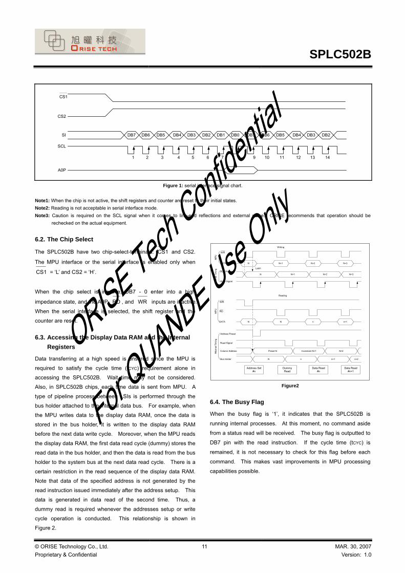
7.1. Display ON/OFF
This command turns the display ON and OFF.
EP RWP
A0P RD WR DB7 DB6 DB5 DB4 DB3 DB2 DB1 DB0 Setting
0 1 0 1 0 1 0 1 1 1 1 Display ON
0 Display OFF
When the display OFF command is executed and when in the display all points ON mode, power saver mode is entered. See the section
on the power saver for details.
7.2. Display Start Line Set
This command is used to specify the display start line address of the display data RAM shown in Figure 4. For further details, see the
explanation of this function in ‘The Line Address Circuit’.
EP RWP
A0P RD WR DB7 DB6 DB5 DB4 DB3 DB2 DB1 DB0 Line Address
0 1 0 0 1 0 0 0 0 0 0 0
0 0 0 0 0 1 1
0 0 0 0 1 0 2
↓ ↓
1 1 1 1 1 0 62
1 1 1 1 1 1 63
7.3. Page Address Set
This command specifies the page address corresponding to the
low address when the MPU accesses the display data RAM (see
Figure 4). Specifying the page address and column address
enables to access a desired bit of the display data RAM.
Changing the page address does not accompany a change in the
status display. See the page address circuit in the Function
Description (page 12) for the detail.
EP RWP
A0P RD WR DB7 DB6 DB5 DB4 DB3 DB2 DB1 DB0 Page Address
0 1 0 1 0 1 1 0 0 0 0 0
0 0 0 1 1
0 0 1 0 2
↓ ↓
0 1 1 1 7
1 0 0 0 8

SPLC502B
© ORISE Technology Co., Ltd. Proprietary & Confidential
25 MAR. 30, 2007Version: 1.0
7.4. Column Address Set
This command specifies the column address of the display data
RAM shown in Figure 4. The column address is split into two
sections (the higher 4 bits and the lower 4 bits) when it is set
(fundamentally, set continuously). Each time the display data RAM
is accessed, the column address automatically incremented (+1),
making it possible for the MPU to continuously read from/write to
the display data. The column address increment is topped at
83H. This does not change the page address continuously.
See the function explanation in ‘The Column Address Circuit’ for
details.
EP RWP Column
A0P RD WR DB7 DB6 DB5 DB4 DB3 DB2 DB1 DB0 A7 A6 A5 A4 A3 A2 A1 A0 Address
High bits → 0 1 0 0 0 0 1 A7 A6 A5 A4 0 0 0 0 0 0 0 0 0 Low bits → 0 A3 A2 A1 A0 0 0 0 0 0 0 0 1 1
0 0 0 0 0 0 1 0 2
↓ ↓
1 0 0 0 0 0 0 0 130
1 0 0 0 0 0 1 1 131
7.5. Status Read
EP RWP
A0P RD WR DB7 DB6 DB5 DB4 DB3 DB2 DB1 DB0
0 0 1 BUSY ADC ON/OFF RESET 0 0 0 0
BUSY When BUSY = ‘1’, it indicates that either processing is occurring internally or a reset condition is in process. While the
chip does not accept commands until BUSY = ‘0’, if the cycle time can be satisfied, there is no need to check for BUSY
condition.
ADC This shows the relationship between the column address and the segment driver.
0: Reverse (column address 131-n SEG n)
1: Normal (column address n SEG n)
(The ADC command switches the polarity.)
ON/OFF ON/OFF: indicates the display ON/OFF state.
0: Display ON
1: Display OFF
(This display ON/OFF command switches the polarity.)
RESET This indicates that the chip is in the process of initialization either because of a RESET signal or because of a reset
command.
0: Operating state
1: Reset in progress

SPLC502B
© ORISE Technology Co., Ltd. Proprietary & Confidential
26 MAR. 30, 2007Version: 1.0
7.6. Display Data Write
This command writes 8-bit data to the specified display data RAM
address. Since the column address is automatically incremented
by one after the write, the MPU can write the display data.
EP RWP
A0P RD WR DB7 DB6 DB5 DB4 DB3 DB2 DB1 DB0
1 1 0 Write data
7.7. Display Data Read
This command reads 8-bit data from the specified display data
RAM address. Since the column address is automatically
incremented by one after the read, the CPU can continuously read
multiple-word data. One dummy read is required immediately
after the column address being set. See the function explanation
in “Display Data RAM” for the explanation of accessing the internal
registers. When the serial interface is used, reading the display
data becomes unavailable.
EP RWP
A0P RD WR DB7 DB6 DB5 DB4 DB3 DB2 DB1 DB0
1 0 1 Read Data
7.8. ADC Select (Segment Driver Direction Select)
This command can reverse the correspondence between the
display RAM data column address and the segment driver output.
Thus, sequence of the segment driver output pins may be
reversed by the command. See the column address circuit (page
12) for the detail. Increment of the column address (by ‘1’)
accompanying the reading or writing the display data is done
according to the column address indicated in Figure 4.
EP RWP
A0P RD WR DB7 DB6 DB5 DB4 DB3 DB2 DB1 DB0 Setting
0 1 0 1 0 1 0 0 0 0 0 Normal
1 Reverse
7.9. Display Normal/Reverse
This command can reverse the lit and unlit display without
overwriting the contents of the display data RAM. When this is
done, the display data RAM contents are maintained.
EP RWP
A0P RD WR DB7 DB6 DB5 DB4 DB3 DB2 DB1 DB0 Setting
0 1 0 1 0 1 0 0 1 1 0 RAM Data ‘H’
LCD ON voltage (normal
1 RAM Data ‘L’
LCD ON voltage (reverse)

SPLC502B
© ORISE Technology Co., Ltd. Proprietary & Confidential
27 MAR. 30, 2007Version: 1.0
7.10. Display All Points ON/OFF
This command makes it possible to force all display points ON
regardless of the content of the display data RAM. The contents of
the display data RAM are maintained when this is done. This
command takes priority over the display normal/reverse
command.
EP RWP
A0P RD WR DB7 DB6 DB5 DB4 DB3 DB2 DB1 DB0 Setting
0 1 0 1 0 1 0 0 1 0 0 Normal display mode
1 Display all points ON
When the display is in an OFF mode, executing the display all
points ON command will place the display in power save mode.
For more details, see the Power Save Section.
7.11. LCD Bias Set
This command selects the voltage bias ratio for the liquid crystal display.
EP RWP Select Status (Duty)
A0P RD WR DB7 DB6 DB5 DB4 DB3 DB2 DB1 DB0 1/65 1/55 1/49 1/33
0 1 0 1 0 1 0 0 0 1 0 1/9 bias 1/8 bias 1/8 bias 1/6 bias
1 1/7 bias 1/6 bias 1/6 bias 1/5 bias
7.12. Read/Modify/Write
This command is used paired with the ‘END’ command. Once
this command has been inputted, the display data read command
does not change the column address, but only the display data
write command increment (+1) the column address. This mode
remains until the END command is inputted. When the END
command is inputted, the column address returns to the address
at when the read/modify/write command was entered. This
function makes it possible to reduce the load on the MPU when
there is repeating data changes in a specified display region, such
as when there is a blanking cursor.
EP RWP
A0P RD WR DB7 DB6 DB5 DB4 DB3 DB2 DB1 DB0
0 1 0 1 1 1 0 0 0 0 0 Note: Even in read/modify/write mode, other commands aside from display data read/write commands can also be used. However, the column address set
command cannot be used.

SPLC502B
© ORISE Technology Co., Ltd. Proprietary & Confidential
28 MAR. 30, 2007Version: 1.0
7.12.1. The sequence for cursor display
Figure 15
7.13. END
This command releases the read / modify / write mode, and returns the column address to the address at when the mode was entered.
EP RWP
A0P RD WR DB7 DB6 DB5 DB4 DB3 DB2 DB1 DB0
0 1 0 1 1 1 0 1 1 1 0
Figure 16
Page address set
Column address set
Read/modify/write
Dummy read
Data read
Data write
Change complete?
End
Yes
No
Data process
N N+1 N+2 N+3 N+m N
Return
EndRead/modify/write mode set
Column address
SPLC502B
© ORISE Technology Co., Ltd. Proprietary & Confidential
29 MAR. 30, 2007Version: 1.0
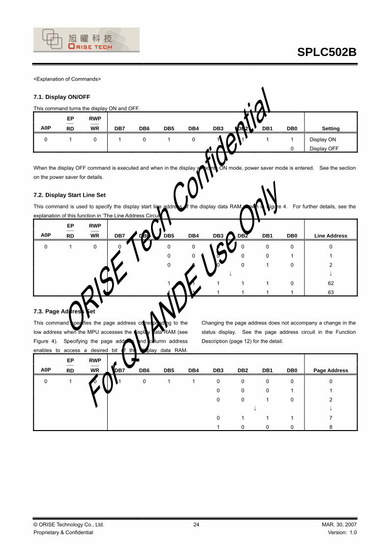
7.14. RESET
This command initializes the display start line, the column address,
the page address, the common output mode, the V0 voltage
regulator internal resistor ratio, the electronic volume, and the
static indicator are reset, and the read/modify/write mode and test
mode are released. There is no impact on the display data RAM.
See the function explanation in “Reset” for details. The reset
operation is performed after the reset command is entered.
EP RWP
A0P RD WR DB7 DB6 DB5 DB4 DB3 DB2 DB1 DB0
0 1 0 1 1 1 0 0 0 1 0
The initialization must be done through applying a reset signal to the RESET terminal when the power supply is applied.
7.15. Common Output Mode Select
This command can select the scan direction of the COM output
terminal. For details, see the function explanation in “Common
Output Mode Select Circuit”.
EP RWP Select Status
A0P RD WR DB7 DB6 DB5 DB4 DB3 DB2 DB1 DB0 SPLC502B
0 1 0 1 1 0 0 0 * * * Normal
1 Reverse Note: *Disabled bit
7.16. Power Controller Set
This command sets the power supply circuit functions. See the function explanation in “The Power Supply Circuit” for more details.
EP RWP
A0P RD WR DB7 DB6 DB5 DB4 DB3 DB2 DB1 DB0 Selected Mode
0 1 0 0 0 1 0 1 0 Booster circuit: OFF
1 Booster circuit: ON
0 Voltage regulator circuit :OFF
1 Voltage regulator circuit: ON
0 Voltage follower circuit: OFF
1 Voltage follower circuit: ON Note: Display off command masks the power control circuits

SPLC502B
© ORISE Technology Co., Ltd. Proprietary & Confidential
30 MAR. 30, 2007Version: 1.0
7.17. V0 Voltage Regulator Internal Resistor Ratio Set
This command sets the V0 voltage regulator internal resistor ratio. For details, see the function explanation in “The Power Supply
Circuits”.
EP RWP
A0P RD WR DB7 DB6 DB5 DB4 DB3 DB2 DB1 DB0 Setting
0 1 0 0 0 1 0 0 0 0 0 Small
0 0 1
0 1 0
↓ ↓
1 1 0
1 1 1 Large
7.18. The Electronic Volume (Double Byte Command)
This command makes it possible to adjust the brightness of the
liquid crystal display by controlling the liquid crystal drive voltage
V0 through the output from the voltage regulator circuits of the
internal liquid crystal power supply. This command is a two bytes
command used as a pair with the electronic volume mode set
command and the electronic volume register set command, and
both commands must be issued one after the other.
7.18.1. The electronic volume mode set
When this command is input, the electronic volume register set
command becomes enabled. Once the electronic volume mode
has been set, no other command except for the electronic volume
register command can be used. Once the electronic volume
register set command has been used to set data into the register,
the electronic volume mode is released.
EP RWP
A0P RD WR DB7 DB6 DB5 DB4 DB3 DB2 DB1 DB0
0 1 0 1 0 0 0 0 0 0 1
7.18.2. Electronic volume register set
By using this command to set six bits of data to the electronic
volume register, the liquid crystal driving voltage, V0, assumes
one of the 64 voltage levels. When this command is input, the
electronic volume mode is released after the electronic volume
register has been set.
EP RWP
A0P RD WR DB7 DB6 DB5 DB4 DB3 DB2 DB1 DB0 | V0|
0 1 0 * * 0 0 0 0 0 1 Small
0 1 0 * * 0 0 0 0 1 0
0 1 0 * * 0 0 0 0 1 1
↓ ↓
0 1 0 * * 1 1 1 1 1 0
0 1 0 * * 1 1 1 1 1 1 Large Note: *Inactive bit

SPLC502B
© ORISE Technology Co., Ltd. Proprietary & Confidential
31 MAR. 30, 2007Version: 1.0
7.18.3. The electronic volume register set sequence
Figure 17
7.19. Static Indicator (Double Byte Command)
This command controls the static drive system indicator display.
The static indicator display is controlled by this command only,
and is independent from other display control commands. This
is used when one of the static indicator liquid crystal drive
electrodes is connected to the FR terminal, and the other is
connected to the FRS terminal. A different pattern is
recommended for the static indicator electrodes than for the
dynamic drive electrodes. If the pattern is too close, it can result
in deterioration of the liquid crystal and of the electrodes. The
static indicator ON command is a double byte command paired
with the static indicator register set command, and thus one must
execute one after the other. The static indicator OFF command
is a single byte command.
7.19.1. Static indicator ON/OFF
When the static indicator ON command is entered, the static
indicator register set command is enabled. Once the static
indicator ON command is entered, no other command aside from
the static indicator register set command can be used. This
mode is cleared when data is set in the register by the static
indicator register set command.
EP RWP
A0P RD WR DB7 DB6 DB5 DB4 DB3 DB2 DB1 DB0 Static Indicator
0 1 0 1 0 1 0 1 1 0 0 OFF
1 ON
7.19.2. Static indicator register set
This command sets two bits of data into the static indicator register, and is used to set the static indicator into a blinking mode.
EP RWP
A0P RD WR DB7 DB6 DB5 DB4 DB3 DB2 DB1 DB0 Static Indicator
0 1 0 * * * * * * 0 0 OFF
* * * * * * 0 1 ON (blinking at approximately one second intervals)
* * * * * * 1 0 ON (blinking at approximately 0.5 second intervals)
* * * * * * 1 1 ON (constantly on) Note: *Disabled bit
7.20. Page Blinking (Double Byte Command)
7.20.1. The page blinking mode set
EP RWP
A0P RD WR DB7 DB6 DB5 DB4 DB3 DB2 DB1 DB0
0 1 0 1 1 0 1 0 1 0 1
Changes complete?
Electronic volume mode set
Electronic volume register set
Electronic volume mode clear
Yes
No

SPLC502B
© ORISE Technology Co., Ltd. Proprietary & Confidential
32 MAR. 30, 2007Version: 1.0
7.20.2. Page blinking register set
Set either bit to '1' will set corresponding PAGE0 - PAGE7 to blink.
EP RWP
A0P RD WR DB7 DB6 DB5 DB4 DB3 DB2 DB1 DB0 Blinking Page
0 1 0 1 0 0 0 0 0 0 0 PAGE 7 blink
0 1 0 0 0 0 0 0 PAGE 6 blink
0 0 1 0 0 0 0 0 PAGE 5 blink
↓
0 0 0 0 0 0 0 1 PAGE 0 blink
7.20.3. Page blinking indicator register set sequence
Figure 18
7.21. Set Driving Mode (Double Byte Command)
This command makes it possible to increase the V0 voltage stability by instruction command for using different liquid crystal panel. User
can select the appropriate mode for their liquid crystal panel and display pattern. The V0 voltage stability is Mode2>Mode1(Default), and so
as the current consumption.
7.21.1. The driving mode set
EP RWP
A0P RD WR DB7 DB6 DB5 DB4 DB3 DB2 DB1 DB0
0 1 0 1 1 0 1 0 0 1 0
7.21.2. Mode selection register set
EP RWP
A0P RD WR DB7 DB6 DB5 DB4 DB3 DB2 DB1 DB0 Driving Duty Selection
0 1 0 0 0 0 0 0 0 0 0 Mode 1
0 0 0 0 0 0 0 1 Mode 2 Note1: DB7 – DB1 7 bits must fill 0. Note2: Mode1 DB0=0 is default. Note3: Driving capability : MODE2 > MODE1.
Changes complete?
Page Blinking mode set
Blinking Page set
(Page Blinking mode clear)
Yes
No

SPLC502B
© ORISE Technology Co., Ltd. Proprietary & Confidential
33 MAR. 30, 2007Version: 1.0
7.22. Power Save (Compound Command)
When the display all points ON is performed while the display is in the OFF mode, the power saver mode is entered and therefore, it
reduces a great amount of power. The power saver mode has two different modes: the sleep mode and the standby mode. When the
static indicator is OFF, the sleep mode is entered. When the static indicator is ON, the standby mode is entered. In the sleep mode and
standby mode, the display data is saved as is the operating mode that was in effect before the power saver mode was initiated, and the
MPU is still able to access the display data RAM. Refer to figure 19 for power save off sequence.
Figure 19
7.22.1. Sleep mode
This stops all operations in the LCD display system, and as long as there are no accesses from the MPU, the consumption current is
reduced to a value close to the static current. The internal modes during sleep mode are as follows:
1). The oscillator circuit and the LCD power supply circuit are halted.
2). All liquid crystal drive circuits are halted, and the segment in common drive outputs output a VSS level.
7.22.2. Standby mode The duty LCD display system operations are halted and only the static drive system for the indicator continues to operate, providing the
minimum required consumption current for the static drive. The internal modes are in the following states during standby mode.
1). The LCD power supply circuits are halted. The oscillator circuit continues to operate.
2). The duty drive system liquid crystal drive circuits are halted and the segment and common driver outputs a VSS level. The static drive
system does not operate.
When a reset command is performed while in standby mode, the system enters sleep mode.
Note1: When an external power supply is used, it is recommended that the functions of the external power supply circuit should be stopped when the power
saver mode is started. For example, when the various levels of liquid crystal drive voltage are provided by external resistive voltage dividers, it is recommended that a circuit be added in order to cut the electrical current flowing through the resistive voltage divider circuit when the power saver
mode is in effect. The SPLC502B chips have a liquid crystal display blanking control terminal DOF . This terminal enters a ‘L’ state when the power
saver mode is launched. Using the output of DOF , it is possible to stop the function of an external power supply circuit.
Note2: When the master is turned on, the oscillator circuit is operable immediately after the power on.
Static indicator OFF Static indicator ON
Power saver (compound command)
Power save OFF(Display all points OFF command)
Power save OFF (compound command)Display all points OFF command
Static indicator ON(2 bytes command)
Sleep mode Standby mode
Standby mode cancelSleep mode cancel

SPLC502B
© ORISE Technology Co., Ltd. Proprietary & Confidential
34 MAR. 30, 2007Version: 1.0
7.23. NOP
Non-Operation Command
EP RWP
A0P RD WR DB7 DB6 DB5 DB4 DB3 DB2 DB1 DB0
0 1 0 1 1 1 0 0 0 1 1
7.24. TEST
This is a command for IC chip testing. Please do not use it. If
the test command is used by accident, it can be cleared by applying a ‘L’ signal to the RESET input by the reset command
or by using a NOP.
EP RWP
A0P RD WR DB7 DB6 DB5 DB4 DB3 DB2 DB1 DB0
0 1 0 1 1 1 1 * * * *
1 1 0 1 0 0 1 0 0
0
1
1
0
0 1 1 0 1 0 1 0 0 Note: The SPLC502B chips maintain their operating modes until some conditions occurred to change them. Consequently, excessive external noise, etc., can
change the internal modes of the SPLC502B chip. Thus, in the packaging and system design, it is necessary to suppress the noise or take measurement to prevent the noise from influencing the chip. Moreover, it is recommended that the operating modes be refreshed periodically to prevent the effects.
7.25. Oscillator Frequency selection
This is a command for Oscillator frequency selection of Driver IC.
EP RWP
A0P RD WR DB7 DB6 DB5 DB4 DB3 DB2 DB1 DB0 Static Indicator
0 1 0 1 1 1 0 0 1 0 0 20KHz/ 33KHz (default)
1 16.4KHz/ 27.06KHz

SPLC502B
© ORISE Technology Co., Ltd. Proprietary & Confidential
35 MAR. 30, 2007Version: 1.0
7.26. Table 13 Table of SPLC502B Commands
Command Code Command
A0P RD WR DB7 DB6 DB5 DB4 DB3 DB2 DB1 DB0Function
1). Display ON/OFF 0 1 0 1 0 1 0 1 1 1 0
1
LCD display ON/OFF
0: OFF, 1: ON
2). Display start line set 0 1 0 0 1 Display start address Sets the display RAM display start line
address
3). Page address set
4). Column address set
upper bit
Column address set
lower bit
0
0
0
1
1
1
0
0
0
1
0
0
0
0
0
1
0
0
1
1
0
Page address
Most significant
column address
Least significant
column address
Sets the display RAM page address
Sets the most significant 4 bits of the
display RAM column address.
Set the least significant 4 bits of the
display RAM column address.
5). Status read 0 0 1 Status 0 0 0 0 Reads the status data
6). Display data write 1 1 0 Write data Writes to the display RAM
7). Display data read 1 0 1 Read data Reads from the display RAM
8). ADC select 0 1 0 1 0 1 0 0 0 0 0
1
Sets the display RAM address SEG
output correspondence
0: normal, 1:reverse
9). Display normal/reverse 0 1 0 1 0 1 0 0 1 1 0
1
Sets the LCD display normal/ reverse
0: normal, 1:reverse
10). Display all points
ON/OFF
0 1 0 1 0 1 0 0 1 0 0
1
Display all points
0: normal display
1: all points ON
11). LCD bias set 0 1 0 1 0 1 0 0 0 1 0
1
Sets the LCD driver voltage bias ratio
SPLC502B……….0:1/9, 1:1/7
12). Read/modify/write 0 1 0 1 1 1 0 0 0 0 0 Column address increment
At write: +1
At read: 0
13). End 0 1 0 1 1 1 0 1 1 1 0 Clear read/modify/write
14). Reset 0 1 0 1 1 1 0 0 0 1 0 Internal reset
15). Common output mode
select
0 1 0 1 1 0 0 0
1
* * * Select COM output scan direction
0: normal direction,
1: reverse direction
16). Power control set 0 1 0 0 0 1 0 1 Operating mode Select internal power supply operating
mode
17). V0 voltage regulator
internal resistor ratio
set
0 1 0 0 0 1 0 0 Resistor ratio Select internal resistor ratio (Rb/Ra)
mode
1 0 0 0 0 0 0 118). Electronic volume
mode set
Electronic volume
register set
0
0
1
1
0
0 * * Electronic volume value
Set the V0 output voltage electronic
volume register
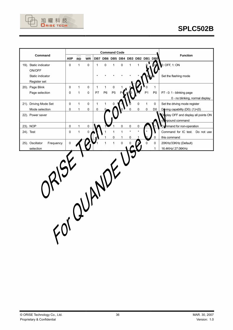
SPLC502B
© ORISE Technology Co., Ltd. Proprietary & Confidential
36 MAR. 30, 2007Version: 1.0
Command Code Command
A0P RD WR DB7 DB6 DB5 DB4 DB3 DB2 DB1 DB0Function
1 0 1 0 1 1 0 0
1
19). Static indicator
ON/OFF
Static indicator
Register set
0 1 0
* * * * * * Mode
0: OFF, 1: ON
Set the flashing mode
20). Page Blink
Page selection
0
0
1
1
0
0
1
P7
1
P6
0
P5
1
P4
0
P3
1
P2
0
P1
1
P0
P7 - 0: 1 - blinking page
0 - no blinking, normal display
21). Driving Mode Set
Mode selection
0
0
1
1
0
0
1
0
1
0
0
0
1
0
0
0
0
0
1
0
0
D0
Set the driving mode register
Driving capability (D0): (1)>(0)
22). Power saver Display OFF and display all points ON
compound command
23). NOP 0 1 0 1 1 1 0 0 0 1 1 Command for non-operation
24). Test 0 1 0 1
1
1
1
1
0
1
1
*
0
*
1
*
0
*
0
Command for IC test. Do not use
this command
25). Oscillator Frequency
selection
0 1 0 1 1 1 0 0 1 0 0
1
20KHz/33KHz (Default)
16.4KHz/ 27.06KHz

SPLC502B
© ORISE Technology Co., Ltd. Proprietary & Confidential
37 MAR. 30, 2007Version: 1.0
8. COMMAND DESCRIPTION 8.1. Instruction Setup: Reference (Reference)
8.1.1. Initialization Note: When the power is applied, LCD driving non-selective potentials V2
and V3 (SEG pin) and V1 and V4 (COM pin) are output through the LCD driving output pins SEG and COM. When electric charge is remaining in the smoothing capacitor connecting between the LCD driving voltage output pins (V0 - 1) and the VDD pin, the picture on the display may become totally dark instantaneously when the power is turned on. To avoid occurrence of such a failure, we recommend the following flow when turning on the power.
1). When the built-in power is being used immediately after turning
on the power:
Turn ON the VDD-VSS power keeping theRESET pin = "L".
When the power is stabilized
Release the reset state. (RESET pin = "H")
Initialized state (Default) *1
Function setup by command input(User setup) (11) LCD bias setting *2 (8) ADC selection *3 (15) Common output state selection *4
Function setup by command input(User setup) (17) Setting the built-in resistance radio for regulation of the V5 voltage *5 (18) Electronic volume control *6
Function setup by command input(User setup) (16) Power control setting *7
This concludes the initialization
Arrange to execute all theprocedures from releasing thereset state through setting thepower control within 5ms.Execute the procedures fromturning on the power to settingthe power control in 5ms.
Figure 20
Note1: The target time of 5ms varied depending on the panel characteristics
and the capacitance of the smoothing capacitor. Therefore, we suggest users to conduct an operation check using the actual equipment.
Note2: Refer to respective sections or paragraphs listed below. *1:Description of functions; Reset circuit *2:Command description; LCD bias setting *3:Command description; ADC selection *4:Command description; Common output state selection *5:Description of functions; Power circuit & Command description;
Setting the built-in resistance radio for regulation of the V0 voltage *6:Description of functions; Power circuit & Command description;
Electronic volume control *7:Description of functions; Power circuit & Command description;
Power control setting.
2). When the built-in power is not being used immediately after
turning on the power:
Turn ON the VDD-VSS power keeping theRESET pin = "L".
When the power is stabilized
Release the reset state. (RESET pin = "H")
Initialized state (Default) *1
Function setup by command input(User setup) (11) LCD bias setting *2 (8) ADC selection *3 (15) Common output state selection *4
Function setup by command input(User setup) (17) Setting the built-in resistance radio for regulation of the V5 voltage *5 (18) Electronic volume control *6
Function setup by command input(User setup) (16) Power control setting *7
This concludes the initialization
Arrange to start the power saverwithin 5ms after releasing thereset state. Execute theprocedures from turning on thepower to setting the powercontrol in 5ms.
Power saver START (multiple commands) *8
Power saver OFF *8
Arrange to start power controlsetting within 5ms after turningOFF the power saver.
Figure 21
Note1: The target time of 5ms varied depending on the panel characteristics and the capacitance of the smoothing capacitor. Therefore, we suggest users to conduct an operation check using the actual equipment.
Note2: Refer to respective sections or paragraphs listed below.
*1:Description of functions; Resetting circuit *2:Command description; LCD bias setting *3:Command description; ADC selection *4:Command description; Common output state selection *5:Description of functions; Power circuit & Command description;
Setting the built-in resistance radio for regulation of the V0 voltage *6:Description of functions; Power circuit & Command description;
Electronic volume control *7:Description of functions; Power circuit & Command description;
Power control setting *8:The power saver ON state can either be in sleep state or stand-by
state. Command description; Power saver START (multiple commands)

SPLC502B
© ORISE Technology Co., Ltd. Proprietary & Confidential
38 MAR. 30, 2007Version: 1.0
8.1.2. Data display
Figure 22
8.1.3. Power OFF *14
Figure 23
Note: Reference items *14:The logic circuit of this IC’s power supply VDD - VSS controls the
driver of the LCD power supply V0. Therefore, if the power supply VDD - VSS is cut off when the LCD power supply V0 has still any residual voltage, the driver (COM. SEG) may output any uncontrolled voltage. When turning off the power, observe the following basic procedures: • After turning off the internal power supply, make sure that the potential V0 - 1 has become below the threshold voltage of the LCD panel, and then turn off this IC’s power supply (VDD - VSS). Refer to “6. Description of Function, Power Circuit” for more information.
*15: After inputting the power save command, be sure to reset the function
using the RESET terminal until the power supply VDD - VSS is
turned off. Refer to “ 7. Command Description, (20) Power Save” for more information.
End of initialization
Function setup by command input (User setup) (6) Display data write *12
Function setup by command input (User setup) (2) Display start line set *9 (3) Page address set *10 (4) Column address set *11
Function setup by command input (User setup) (1) Display ON/OFF *13
End of data display
Notes: Reference items*9: Command Description; Display start line set*10: Command Description; Page address set*11:Command Description; Column address set*12: Command Description; Display data write*13: Command Description; Display ON/OFF Avoid displaying all the data at the data display start(when the display is ON) in white.
Set the time (tL) from reset active toturning off the VDD - VSS Power ( VDD -VSS = 2.4 V) longer than the time (tH)when the potential of V5 - 1 becomes belowthe threshold voltage (approximately 1V)of the LCD panel. For tH, refer to the<Reference Data> of this event. When tHis too long, insert a resistor between V5
and VDD to reduct it.
Optional status
VDD - VSS power OFF
Function setup by command input (User setup) (20) Power save *15
Reset active( pin = "L")RESET

SPLC502B
© ORISE Technology Co., Ltd. Proprietary & Confidential
39 MAR. 30, 2007Version: 1.0
9. ELECTRICAL SPECIFICATIONS 9.1. Absolute Maximum Ratings
(Unless otherwise noted, VSS = 0V)
Parameter Symbol Conditions Unit
Power Supply Voltage VDD -0.3 to + 3.6 V
Power supply voltage (2)
(VDD standard)
With Triple step-up
With Quad step-up
VDD2
-0.3 to + 3.6
-0.3 to + 3.6
-0.3 to + 3.0
V
Power supply voltage (3) (VDD standard) V0, VLCD -0.3 to + 12 V
Power supply voltage (4) (VDD standard) V1, V2, V3, V4 -0.3 to V0 V
Input voltage VIN -0.3 to VDD +0.3 V
Output voltage VO -0.3 to VDD +0.3 V
Operating temperature TOPR -20 to +75
Storage temperature Bare chip TSTR -55 to +125
Notes and Cautions: 1. The VDD2, V0 to V4 and VOUT are relative to the VSS = 0V reference. 2. Insure that the voltage levels of V0, V1, V2, V3, and V4 are always such that V0≧V1≧V2≧V3≧V4≧VSS(GND)
3. Permanent damage to the LSI may result if the LSI is used outside of the absolute maximum ratings. Moreover, it is recommended that in normal operation the chip be used at the electrical characteristic conditions, and use of the LSI outside of these conditions may not only result in malfunctions of the LSI, but may have a negative impact on the LSI reliability as well.
9.2. DC Characteristics
(Unless otherwise specified, VSS = 0V, VDD = 3.0V±10%, TA = -20 to 75)
Rating Item Symbol Condition
Min. Typ. Max. Units
Applicable
PIN
Operating
Voltage (1)
Recommended
Voltage VDD
1.8
-
3.6
V
VDD*1
Operating
Voltage (2)
Recommended
Voltage
VDD2
(Relative to VSS)
1.8
-
3.6
V
VDD2
Operating
Voltage (3)
Possible Operating
Voltage
V0 (Relative to VSS)
4.0
- 12.0
V
V0*2
High-level Input Voltage
Low-level Input Voltage
VIHC
VILC
0.8 x VDD
VSS
-
-
VDD
0.2 x VDD
V
V
*3
*3
High-level output Voltage
Low-level output Voltage
VOHC
VOLC
IOH = -0.5mA
IOL = 0.5mA
0.8 x VDD
VSS
-
-
VDD
0.2 x VDD
V
V
*4
*4
Input leakage current
Output leakage current
ILI
ILO
VIN = VDD or VSS -1.0
-3.0
-
-
1.0
3.0
µA
µA
*5
*6
Liquid Crystal Driver ON
Resistance RON
TA = 25
(Relative To VSS)
V0 = 12V
V0 = 8.0V
-
-
2.0
3.2
3.5
5.4
KΩ
KΩ
SEGn
COMn*7
Static Consumption Current
Output Leakage Current
ISSQ
I0Q
V0 = 12V (Relative to VSS)
-
-
0.01
0.01
5.0
15
µA
µA
VDD, VDD2
V0
Input Terminal Capacitance CIN TA = 25 f = 1.0MHz - 5.0 8.0 pF
Internal Oscillator
External Input
fOSC
fCL
1/65 duty TA = 25
1/33 duty
17
17
20
20
23
23
KHz
KHz
*8
CL
Oscillator
Frequency
Internal Oscillator
External Input
fOSC
fCL
1/55 duty TA = 25
1/49 duty
28
28
33
33
38
38
KHz
KHz
*8
CL

SPLC502B
© ORISE Technology Co., Ltd. Proprietary & Confidential
40 MAR. 30, 2007Version: 1.0
Rating Item Symbol Condition
Min. Typ. Max. Units
Application
PIN
Input Voltage VDD2
VDD2
With Triple (Relative to VSS)
With Quad (Relative to VSS)
1.8
1.8
-
-
4.0
3.0
V
V
VDD2
VDD2
Supply Setup-up output
voltage Circuit VOUT (Relative to VSS) - - 13.0 V VOUT
Voltage regulator Circuit
Operating Voltage VOUT (Relative to VSS) 4.0 - 13.0 V VOUT
Voltage Follower Circuit
Operating Voltage V0 (Relative to VSS) 4.0 - 12.0 V V0 *9
Inte
rnal
Pow
er
Base Voltage VREG0 TA = 25
(Relative to VSS) -0.05%/ 2.08 2.1 2.12 V *10
9.3. Display Pattern Checker
(TA = -20 to 75)
Rating Item Symbol Condition
Min. Typ. Max. Units Notes
SPLC502B IDD(1+2) VDD = 3.0V, V0 - VSS = 11V - 20 25 µA *11
Dynamic Consumption Current (1+2), During Display, with the Internal Power Supply OFF.
Current consumed by total ICs when an external power supply is used.
9.4. Display Pattern Checker (TA = -20 to 75)
Rating Item Symbol Condition
Min. Typ. Max. Units Notes
SPLC502B IDD(1+2) VDD = 3.0V, Quad step-up
voltage. V0 = 11.0V
Normal Mode - 130 160 µA *11
Dynamic Consumption Current (1+2), During Display, with the Internal Power Supply ON
Rating Item Symbol Condition
Min. Typ. Max. Units Notes
Sleep Mode SPLC502B IDDS1 - - 0.01 5.0 µA
Item fCL fFR
When the internal oscillator circuit is used (20KHz) fOSC / 4 fOSC / (4 * 65) 1/65 DUTY *8
When the internal oscillator circuit is not used External input (fCL) fCL / 260
When the internal oscillator circuit is used (33KHz) fOSC / 8 fOSC / (8 * 55) 1/55 DUTY *8
When the internal oscillator circuit is not used External input (fCL) fCL / 220
When the internal oscillator circuit is used (33KHz) fOSC / 8 fOSC / (8 * 49) 1/49 DUTY *8
When the internal oscillator circuit is not used External input (fCL) fCL / 196
When the internal oscillator circuit is used (20KHz) fOSC / 8 fOSC / (8 * 33) 1/33 DUTY *8
When the internal oscillator circuit is not used External input (fCL) fCL / 264

SPLC502B
© ORISE Technology Co., Ltd. Proprietary & Confidential
41 MAR. 30, 2007Version: 1.0
References for items market with * *1 While a broad range of operating voltages is guaranteed, performance cannot be guaranteed if there are sudden fluctuations to the voltage while the MPU is
being accessed. *2 The operating voltage range for the VDD system and the V0 system is applied when the external power supply is being used.
*3 The A0P, DB0 to DB5, DB6 (SCL), DB7 (SI), RD (EP), WR (RWP), CS1, CS2, CLS, CL, FR, MS, C86, PS, DOF , RES , and HPM terminals.
*4 The DB0 to DB7, FR, FRS, DOF , and CL terminals.
*5 The A0P, RD (EP), WR (RWP), CS1, CS2, CLS, MS, C86, PS, RES , and HPM terminals.
*6 Applies when the DB0 to DB5, DB6 (SCL), DB7 (SI), CL, FR, and DOF terminals are in a high impedance state.
*7 These are the resistance values for when a 0.1V voltage is applied between the output terminal SEGn or COMn and the various power supply terminals (V1, V2, V3, and V4). These are specified for the operating voltage (3) range.
RON = 0.1V/ I (Where I is the current that flows when 0.1V is applied while the power supply is ON.)
*8 The relationship between the oscillator frequency and the frame rate frequency. *9 The V0 voltage regulator circuit regulates within the operating voltage range of the voltage follower. *10 This is the internal voltage reference supply for the V0 voltage regulator circuit. In the SPLC502B, the temperature range can come in three types as
VREG options: (1) approximately –0.05%/C. *11 It indicates the current consumed on ICs alone when the internal oscillator circuit and display are turned on.
The SPLC502B is 1/9 biased. Does not include the current due to the LCD panel capacity and wiring capacity. Applicable only when there is no access from the MPU. V1~V4 without capacitor.
*12 It is the value on a model having the VREG option temperature gradient is –0.05%/C when the V0 voltage regulator internal resistor is used.

SPLC502B
© ORISE Technology Co., Ltd. Proprietary & Confidential
42 MAR. 30, 2007Version: 1.0
9.5. Timing Characteristics
9.5.1. System bus read/write characteristics 1 (For the 8080 Series MPU)
(VDD = 3.3V to 3.6V, TA = -20 to 75)
Rating Item Signal Symbol Condition
Min. Max. Units
Address hold time
Address setup time A0P
tAH8
tAW8
0
0
-
-
ns
ns
System cycle time A0P tCYC8 240 - ns
Control L pulse width ( WR )
Control L pulse width ( RD )
Control H pulse width ( WR )
Control H pulse width ( RD )
WR
RD
WR
RD
tCCLW
tCCLR
tCCHW
tCCHR
80
80
80
80
-
-
-
-
ns
ns
ns
ns
Data setup time
Address hold time
tDS8
tDH8
30
10
-
-
ns
ns
RD access time
Output disable time
DB7 - 0 tACC8
tOH8 CL = 100pF
-
5.0
70
50
ns
ns
A0P
DB7 - 0(Write)
tAW8
DB7 - 0(Read)
tACC8
tDS8
tCCLR, tCCLW
tAH8
tOH8
tDS8
tCCHR , tCCHW
tCYC8
WR, RD
(CS2="1")CS1

SPLC502B
© ORISE Technology Co., Ltd. Proprietary & Confidential
43 MAR. 30, 2007Version: 1.0
(VDD = 2.7V to 3.3V, TA = -20 to 75)
Rating Item Signal Symbol Condition
Min. Max. Units
Address hold time
Address setup time A0P
tAH8
tAW8
0
0
-
-
ns
ns
System cycle time A0P tCYC8 400 - ns
Control L pulse width ( WR )
Control L pulse width ( RD )
Control H pulse width ( WR )
Control H pulse width ( RD )
WR
RD
WR
RD
tCCLW
tCCLR
tCCHW
tCCHR
100
100
100
100
-
-
-
-
ns
ns
ns
ns
Data setup time
Address hold time
tDS8
tDH8
40
15
-
-
ns
ns
RD access time
Output disable time
DB7 - 0 tACC8
tOH8 CL = 100pF
-
10
140
100
ns
ns
(VDD = 1.8V to 2.7V, TA = -20 to 75)
Rating Item Signal Symbol Condition
Min. Max. Units
Address hold time
Address setup time
A0P tAH8
tAW8
0
0
-
-
ns
ns
System cycle time A0P tCYC8 640 - ns
Control L pulse width ( WR )
Control L pulse width ( RD )
Control H pulse width ( WR )
Control H pulse width ( RD )
WR
RD
WR
RD
tCCLW
tCCLR
tCCHW
tCCHR
200
200
200
200
-
-
-
-
ns
ns
ns
ns
Data setup time
Address hold time
tDS8
tDH8
80
30
-
-
ns
ns
RD access time
Output disable time
DB7 - 0 tACC8
tOH8 CL = 100pF
-
10
280
200
ns
ns Note1: The input signal rise time and fall time (tr, tf) is specified at 15 ns or less. When the system cycle time is extremely fast, (tr + tf)≦(tCYC8 - tCCLW - tCCHW) for (tr
+ tf)≦(tCYC8 - tCCLR - tCCHR) are specified.
Note2: All timing is specified using 20% and 80% of VDD as the reference.
Note3: tCCLW and tCCLR are specified as the overlap between CS1 being 'L' ( CS2 = 'H') and WR and RD being at the 'L' level.

SPLC502B
© ORISE Technology Co., Ltd. Proprietary & Confidential
44 MAR. 30, 2007Version: 1.0
9.5.2. System bus read/write characteristics 2 (6800 series MPU)
(VDD = 3.3V to 3.6V, TA = -20 to 75)
Rating Item Signal Symbol Condition
Min. Max. Units
Address hold time
Address setup time A0P
tAH6
tAW6
0
0
-
-
ns
ns
System cycle time A0P tCYC6 240 - ns
Data setup time
Data hold time
tDS6
tDH6 CL = 100pF
30
10
-
-
ns
ns
Access time
Output disable time
DB7 - 0 tACC6
tOH6
-
10
70
50
ns
ns
Enable H pulse time Read
Write EP
tEWHR
tEWHW
80
80
-
-
ns
ns
Enable L pulse time Read
Write EP
tEWLR
tEWLW
80
80
-
-
ns
ns
A0P
(CS2="1")CS1
DB7 - 0(Write)
tAW6
DB7 - 0(Read)
tACC6
tDS6
tEWHR, tEWHW
tAH6
tOH6
tDH6
tCYC6
tEWLR , tEWLW
RWP
EP

SPLC502B
© ORISE Technology Co., Ltd. Proprietary & Confidential
45 MAR. 30, 2007Version: 1.0
(VDD = 2.7V to 3.3V, TA = -20 to 75)
Rating Item Signal Symbol Condition
Min. Max. Units
Address hold time
Address setup time A0P
tAH6
tAW6
0
0
-
-
ns
ns
System cycle time A0P tCYC6 400 - ns
Data setup time
Data hold time
tDS6
tDH6 CL = 100pF
40
15
-
-
ns
ns
Access time
Output disable time
DB7 - 0 tACC6
tOH6
-
10
140
100
ns
ns
Enable H pulse time Read
Write EP
tEWHR
tEWHW
100
100
-
-
ns
ns
Enable L pulse time Read
Write EP
tEWLR
tEWLW
100
100
-
-
ns
ns
(VDD = 1.8V to 2.7V, TA = -20 to 75)
Rating Item Signal Symbol Condition
Min. Max. Units
Address hold time
Address setup time A0P
tAH6
tAW6
0
0
-
-
ns
ns
System cycle time A0P tCYC6 640 - ns
Data setup time
Data hold time
tDS6
tDH6 CL = 100pF
80
30
-
-
ns
ns
Access time
Output disable time
DB7 - 0 tACC6
tOH6
-
10
280
120
ns
ns
Enable H pulse time Read
Write EP
tEWHR
tEWHW
200
200
-
-
ns
ns
Enable L pulse time Read
Write EP
tEWLR
tEWLW
200
200
-
-
ns
ns Note1: The input signal rise time and fall time (tr, tf) is specified at 15 ns or less. When the system cycle time is extremely fast, (tr + tf)≦(tCYC6 - tEWLW - tEWHW) for
(tr + tf)≦(tCYC6 - tEWLR - tEWHR) are specified.
Note2: All timing is specified using 20% and 80% of VDD as the reference.
Note3: tEWLW and tEWLR are specified as the overlap between CS1 being 'L' (CS2 = 'H') and EP.

SPLC502B
© ORISE Technology Co., Ltd. Proprietary & Confidential
46 MAR. 30, 2007Version: 1.0
9.5.3. The serial interface
(VDD = 3.3V to 3.6V, TA = -20 to 75)
Rating Item Signal Symbol Condition
Min. Max. Units
Serial Clock Period
SCL 'H' pulse width
SCL 'L' pulse width
SCL
tSCYC
tSHW
tSLW
-
-
-
200
80
80
-
-
-
ns
ns
ns
Address setup time
Address hold time A0P
tSAS
tSAH
-
-
50
100
-
-
ns
ns
Data setup time
Data hold time SI
tSDS
tSDH
-
-
50
50
-
-
ns
ns
CS-SCL time CS tCSS
tCSH
-
-
100
100
-
-
ns
ns
(VDD = 2.7V to 3.3V, TA = -20 to 75)
Rating Item Signal Symbol Condition
Min. Max. Units
Serial Clock Period
SCL 'H' pulse width
SCL 'L' pulse width
SCL
tSCYC
tSHW
tSLW
-
-
-
250
100
100
-
-
-
ns
ns
ns
Address setup time
Address hold time A0P
tSAS
tSAH
-
-
150
150
-
-
ns
ns
Data setup time
Data hold time SI
tSDS
tSDH
-
-
100
100
-
-
ns
ns
CS-SCL time CS tCSS
tCSH
-
-
150
150
-
-
ns
ns
tSDS tSDH
tR
tSHW
tF
tSLW
tSCYC
tSAS tSAH
tCSS tCSH
(CS2="1")CS1
A0
SCL
SI

SPLC502B
© ORISE Technology Co., Ltd. Proprietary & Confidential
47 MAR. 30, 2007Version: 1.0
(VDD = 1.8V to 2.7V, TA = -20 to 75)
Rating Item Signal Symbol Condition
Min. Max. Units
Serial Clock Period
SCL 'H' pulse width
SCL 'L' pulse width
SCL
tSCYC
tSHW
tSLW
-
-
-
350
150
150
-
-
-
ns
ns
ns
Address setup time
Address hold time A0P
tSAS
tSAH
-
-
150
150
-
-
ns
ns
Data setup time
Data hold time SI
tSDS
tSDH
-
-
60
30
-
-
ns
ns
CS-SCL time CS tCSS
tCSH
-
-
250
250
-
-
ns
ns Note1: The input signal rise and fall time (tr, tf) are specified at 15 ns or less. Note2: All timing is specified using 20% and 80% of VDD as the standard.
9.5.4. Display control output timing
(VDD = 3.3V to 3.6V, TA = -20 to 75)
Rating Item Signal Symbol Condition
Min. Typ. Max. Units
FR delay time FR tDFR CL = 50pF - 10 40 ns
(VDD = 2.7V to 3.3V, TA = -20 to 75)
Rating Item Signal Symbol Condition
Min. Typ. Max. Units
FR delay time FR tDFR CL = 50pF - 20 80 ns
(VDD = 1.8V to 2.7V, TA = -20 to 75)
Rating Item Signal Symbol Condition
Min. Typ. Max. Units
FR delay time FR tDFR CL = 50pF - 50 200 ns Note1: Valid only when the master mode is selected. Note2: All timing is based on 20% and 80% of VDD.
CL(OUT)
tDFR
FR

SPLC502B
© ORISE Technology Co., Ltd. Proprietary & Confidential
48 MAR. 30, 2007Version: 1.0
9.5.5. Reset timing
(VDD = 3.3 V to 3.6V, TA = -20 to 75)
Rating Item Signal Symbol Condition
Min. Typ. Max. Units
Reset time tR - - 0.5 µs
Reset 'L' pulse width RES tRW -
0.5 - - µs
(VDD = 2.7V to 3.3V, TA = -20 to 75)
Rating Item Signal Symbol Condition
Min. Typ. Max. Units
Reset time tR - - 1.0 µs
Reset 'L' pulse width RES tRW -
1.0 - - µs
(VDD = 1.8V to 2.7V, TA = -20 to 75)
Rating Item Signal Symbol Condition
Min. Typ. Max. Units
Reset time tR - - 1.5 µs
Reset 'L' pulse width RES t -
1.5 - - µs Note: All timing is specified with 20% and 80% of VDD as the standard. 9.6. The MPU Interface (Reference Examples)
The SPLC502B can be connected to either 80X86 Series MPUs or
to 68000 Series MPUs. Moreover, The serial interface is possible
to operate the SPLC502B chips with fewer signal lines. The
display area can be enlarged by using multiple SPLC502B chips.
When this is done, the chip select signal can be used to select the
individual ICs to access.
Internalstatus
RESET
During reset Reset complete
tRW
tR

SPLC502B
© ORISE Technology Co., Ltd. Proprietary & Confidential
49 MAR. 30, 2007Version: 1.0
9.6.1. 8080 series MPUs
Figure 26
9.6.2. 6800 series MPUs
Figure 27
MP
U
SPLC
502B
VSS
Decoder
RESET
MP
U
SPLC
502B
GND
A0P
A15 - 1VMA
DB7 - 0E
R/W
CS1CS2
DB7 - 0EPRWP
C86
PS
A0P
RESETRESET
VDD
VDDVCC
VSS

SPLC502B
© ORISE Technology Co., Ltd. Proprietary & Confidential
50 MAR. 30, 2007Version: 1.0
9.6.3. Using the serial interface
Figure 28
9.7. Connections between LCD Drivers (Reference Example)
The liquid crystal display area can be enlarged with ease through the use of multiple SPLC502B chips. Use a same equipment type.
9.7.1. SPLC502B (Master)<->SPLC502B (Slave)
Figure 29
MPU
SP
LC50
2B
SP
LC50
2B
Mas
ter
SP
LC50
2B
Sla
ve

SPLC502B
© ORISE Technology Co., Ltd. Proprietary & Confidential
51 MAR. 30, 2007Version: 1.0
9.8. Connections between LCD Drivers (Reference Examples)
The liquid crystal display area can be enlarged with ease through the use of multiple SPLC502B chips. Use a same equipment type, in the
composition of these chips.
9.8.1. Single-chip structure Figure 30
9.8.2. Double-chip structure
Figure 31

SPLC502B
© ORISE Technology Co., Ltd. Proprietary & Confidential
52 MAR. 30, 2007Version: 1.0
10. VLCD Voltage (Voltage between V0 to VSS) relationship of V0 Voltage Regulator Internal Resistor Ratio Register and Electronic Volume Control Register
Note: Use External VOUT Power Supply.
0.000
2.000
4.000
6.000
8.000
10.000
12.000
14.000
1 4 7 10 13 16 19 22 25 28 31 34 37 40 43 46 49 52 55 58 61 64
000
001
010
011
100
101
110
111
The V0 voltage
regulator internal
resistance ratio
registers
(D2, D1, D0)

SPLC502B
© ORISE Technology Co., Ltd. Proprietary & Confidential
53 MAR. 30, 2007Version: 1.0
11. CHIP INFORMATION 11.1. PAD Assignment
TE
ST
DU
MY
9D
UM
Y8
DU
MY
7D
UM
Y6
DU
MY
5D
UM
Y4
DU
MY
3D
UM
Y2
DU
MY
1
TE
ST
6T
ES
T5
VD
DH
PM
PS
C86
CL
SM
SV
SS
V0
V0
V4
V3
V3
V2
V2
V1
V1
VD
DV
DD
VD
DA
VD
DA
VS
SV
SS
VS
SA
VS
SA
CA
P4
PC
AP
4P
CA
P2
NC
AP
2N
CA
P2
PC
AP
2P
CA
P1
P
CA
P1P
CA
P1
N
CA
P5
PC
AP
5P
CA
P4P
VO
UT
VO
UT
VO
UT
VS
SA
VS
SA
VS
SA
VS
SV
SS
VS
SV
DD
AV
DD
AV
DD
AV
DD
VD
DV
DD
DS
EL1
DS
EL0
DB
7D
B6
DB
5D
B4
DB
3D
B2
DB
1D
B0
VD
DE
PR
WP
VS
SA
OP
RE
SE
TV
DD
CS
2C
S1
VS
SD
OF
CL
FR
FR
S
94
COM22COM21COM20COM19COM18COM17COM16COM15COM14COM13COM12COM11COM10
CA
P1
NC
AP
3P
CA
P3P
DU
MY
10
291
COM55COM54COM53COM52COM51COM50COM49COM48COM47COM46COM45COM44COM43
COM58COM57COM56
270
107
CO
M6
CO
M5
CO
M4
CO
M3
CO
M2
CO
M1
CO
M0
CO
MS
1S
EG
0S
EG
1S
EG
2S
EG
3S
EG
4S
EG
5S
EG
6S
EG
7S
EG
8S
EG
9S
EG
10S
EG
11S
EG
12S
EG
1 3S
EG
14S
EG
1 5S
EG
16S
EG
17S
EG
18S
EG
19S
EG
2 0S
EG
21S
EG
22S
EG
23S
EG
24S
EG
25S
EG
26S
EG
27
SE
G2 8
SE
G29
SE
G30
SE
G31
SE
G3
2S
EG
33S
EG
34S
EG
35S
EG
3 6S
EG
37S
EG
38S
EG
39
SE
G40
SE
G4
1
SE
G42
SE
G43
SE
G44
SE
G45
SE
G46
SE
G4
7S
EG
48S
EG
49S
EG
50S
EG
51
SE
G5
2S
EG
53
SE
G5
4S
EG
55S
EG
5 6S
EG
57
SE
G58
SE
G59
SE
G6
0S
EG
61
SE
G6
2S
EG
63S
EG
64S
EG
65S
EG
66S
EG
67
SE
G6
8S
EG
69
SE
G7
0S
EG
71
SE
G7
2
SE
G7
3S
EG
74
SE
G7
5S
EG
76
SE
G7
7S
EG
78
SE
G79
SE
G80
SE
G81
SE
G8
2S
EG
83
SE
G8
4S
EG
85
SE
G8
6S
EG
87
SE
G8
8
SE
G8
9S
EG
90
SE
G9
1S
EG
92
SE
G9
3
SE
G9
5S
EG
96
SE
G9
7S
EG
98
SE
G9
9S
EG
10 0
SE
G1
01S
EG
10 2
SE
G1
03S
EG
104
SE
G1
05S
EG
106
SE
G1
07S
EG
108
SE
G1
09S
EG
11 0
SE
G11
1S
EG
112
SE
G1
13S
EG
11
4S
EG
11
5S
EG
11
6S
EG
11
7S
EG
11
8S
EG
11
9S
EG
12
0S
EG
121
SE
G1
22
SE
G1
23
SE
G1
24
SE
G1
25
SE
G1
26
SE
G1
27
SE
G1
28
SE
G1
29
SE
G1
30
SE
G1 3
1
SE
G9
4
81 16 1
COM60COM59
COM63COM62COM61
COMS2
CO
M3
2C
OM
3 3C
OM
34C
OM
35C
OM
36
CO
M37
CO
M38
CO
M39
CO
M40
CO
M4 1
CO
M42
CO
M9
CO
M8
CO
M7
COM28COM27COM26COM25COM24COM23
COM31COM30COM29
V4
DU
MY
11
93
115
127
116
258
269
( 0 ,0 )
SPLC502B
11.2. PAD Dimension
Size Item PAD No.
X Y Unit
Chip Size - 5965 930
Chip thickness - 483 ± 25µm
1 ~ 82 55
83 ~ 93 (Test Pins) 40
Pad pitch 94 ~ 115
270 ~ 291
116 ~ 269
34
1 ~ 82 40 100
83 ~ 93 25 63.6
94 ~ 115
270 ~ 291 135 19
Bumped pad size
116 ~ 269 19 135
µm
Note1: Chip size included scribe line. Note2: To ensure that the IC functions properly, please bond all of VDD, VSS, AVDD and AVSS pins. Note3: The 0.1µF capacitor between VDD and VSS should be placed to IC as close as possible.
11.3. Bump Characteristic
Item Standard Note
Bump Hardness 50HV ±15HV
Bump Height 18µm ±3µm
Co-planarity (in Chip) R 2µm≦ R : Max-Min
Roughness (in Bump) R 2µm≦ R : Max-Min
Bump Size “X” ± 4µm x “Y” ± 4µm X/Y: bump size
Shear Force >4.5g/mil^2

SPLC502B
© ORISE Technology Co., Ltd. Proprietary & Confidential
54 MAR. 30, 2007Version: 1.0
11.4. PAD Locations
PAD No. PAD Name X Y
1 TEST 2552.84 344.15 2 FRS 2497.84 344.15 3 FR 2442.84 344.15 4 CL 2387.84 344.15 5 2332.84 344.15 6 VSS 2277.84 344.15 7 2222.84 344.15 8 CS2 2167.84 344.15 9 VDD 2112.84 344.15 10 2057.84 344.15 11 A0P 2002.84 344.15 12 VSS 1947.84 344.15 13 RWP 1892.84 344.15 14 EP 1837.84 344.15 15 VDD 1782.73 344.15 16 DB0 1727.84 344.15 17 DB1 1672.84 344.15 18 DB2 1617.84 344.15 19 DB3 1562.84 344.15 20 DB4 1507.84 344.15 21 DB5 1452.84 344.15 22 DB6 1397.84 344.15 23 DB7 1342.84 344.15 24 DSEL0 1287.84 344.15 25 DSEL1 1232.84 344.15 26 VDD 1177.84 344.15 27 VDD 1122.84 344.15 28 VDD 1067.84 344.15 29 VDDA 1012.84 344.15 30 VDDA 957.84 344.15 31 VDDA 902.84 344.15 32 VSS 847.84 344.15 33 VSS 792.84 344.15 34 VSS 737.84 344.15 35 VSSA 682.84 344.15 36 VSSA 627.84 344.15 37 VSSA 572.84 344.15 38 VOUT 517.84 344.15 39 VOUT 462.84 344.15 40 VOUT 407.84 344.15 41 CAP4P 352.84 344.15 42 CAP5P 297.84 344.15 43 CAP5P 242.84 344.15 44 CAP3P 187.84 344.15 45 CAP3P 132.84 344.15 46 CAP1N 68.57 344.15 47 CAP1N 13.57 344.15 48 CAP1P -50.68 344.15
PAD No. PAD Name X Y
49 CAP1P -105.68 344.15 50 CAP2P -160.68 344.15 51 CAP2P -215.68 344.15 52 CAP2N -279.95 344.15 53 CAP2N -334.95 344.15 54 CAP4P -399.2 344.15 55 CAP4P -454.2 344.15 56 VSSA -509.2 344.15 57 VSSA -564.2 344.15 58 VSS -619.2 344.15 59 VSS -674.2 344.15 60 VDDA -729.2 344.15 61 VDDA -784.2 344.15 62 VDD -841 344.15 63 VDD -896 344.15 64 V1 -955.54 344.15 65 V1 -1010.54 344.15 66 V2 -1065.54 344.15 67 V2 -1120.54 344.15 68 V3 -1175.54 344.15 69 V3 -1230.54 344.15 70 V4 -1285.54 344.15 71 V4 -1340.54 344.15 72 V0 -1395.54 344.15 73 V0 -1450.54 344.15 74 VSS -1505.54 344.15 75 MS -1560.54 344.15 76 CLS -1615.54 344.15 77 C86 -1670.54 344.15 78 PS -1725.54 344.15 79 -1780.54 344.15 80 VDD -1835.54 344.15 81 TEST5 -1890.55 344.15 82 TEST6 -1945.55 344.15 83 DUMY1 -2018.99 362.35 84 DUMY2 -2058.99 362.35 85 DUMY3 -2098.99 362.35 86 DUMY4 -2138.99 362.35 87 DUMY5 -2178.99 362.35 88 DUMY6 -2218.99 362.35 89 DUMY7 -2258.99 362.35 90 DUMY8 -2298.99 362.35 91 DUMY9 -2338.99 362.35 92 DUMY10 -2378.99 362.35 93 DUMY11 -2421.1 362.35 94 COM31 -2846.45 357 95 COM30 -2846.45 323 96 COM29 -2846.45 289

SPLC502B
© ORISE Technology Co., Ltd. Proprietary & Confidential
55 MAR. 30, 2007Version: 1.0
PAD No. PAD Name X Y
97 COM28 -2846.45 255
98 COM27 -2846.45 221 99 COM26 -2846.45 187 100 COM25 -2846.45 153 101 COM24 -2846.45 119 102 COM23 -2846.45 85 103 COM22 -2846.45 51 104 COM21 -2846.45 17 105 COM20 -2846.45 -17 106 COM19 -2846.45 -51 107 COM18 -2846.45 -85 108 COM17 -2846.45 -119 109 COM16 -2846.45 -153 110 COM15 -2846.45 -187 111 COM14 -2846.45 -221 112 COM13 -2846.45 -255 113 COM12 -2846.45 -289 114 COM11 -2846.45 -323 115 COM10 -2846.45 -357 116 COM9 -2601.32 -328.95 117 COM8 -2567.32 -328.95 118 COM7 -2533.32 -328.95 119 COM6 -2499.32 -328.95 120 COM5 -2465.32 -328.95 121 COM4 -2431.32 -328.95 122 COM3 -2397.32 -328.95 123 COM2 -2363.32 -328.95 124 COM1 -2329.32 -328.95 125 COM0 -2295.32 -328.95 126 COMS1 -2261.32 -328.95 127 SEG0 -2227.32 -328.95 128 SEG1 -2193.32 -328.95 129 SEG2 -2159.32 -328.95 130 SEG3 -2125.32 -328.95 131 SEG4 -2091.32 -328.95 132 SEG5 -2057.32 -328.95 133 SEG6 -2023.32 -328.95 134 SEG7 -1989.32 -328.95 135 SEG8 -1955.32 -328.95 136 SEG9 -1921.32 -328.95 137 SEG10 -1887.32 -328.95 138 SEG11 -1853.32 -328.95 139 SEG12 -1819.32 -328.95 140 SEG13 -1785.32 -328.95 141 SEG14 -1751.32 -328.95 142 SEG15 -1717.32 -328.95 143 SEG16 -1683.32 -328.95 144 SEG17 -1649.32 -328.95 145 SEG18 -1615.32 -328.95 146 SEG19 -1581.32 -328.95
PAD No. PAD Name X Y
147 SEG20 -1547.32 -328.95
148 SEG21 -1513.32 -328.95 149 SEG22 -1479.32 -328.95 150 SEG23 -1445.32 -328.95 151 SEG24 -1411.32 -328.95 152 SEG25 -1377.32 -328.95 153 SEG26 -1343.32 -328.95 154 SEG27 -1309.32 -328.95 155 SEG28 -1275.32 -328.95 156 SEG29 -1241.32 -328.95 157 SEG30 -1207.32 -328.95 158 SEG31 -1173.32 -328.95 159 SEG32 -1139.32 -328.95 160 SEG33 -1105.32 -328.95 161 SEG34 -1071.32 -328.95 162 SEG35 -1037.32 -328.95 163 SEG36 -1003.32 -328.95 164 SEG37 -969.32 -328.95 165 SEG38 -935.32 -328.95 166 SEG39 -901.32 -328.95 167 SEG40 -867.32 -328.95 168 SEG41 -833.32 -328.95 169 SEG42 -799.32 -328.95 170 SEG43 -765.32 -328.95 171 SEG44 -731.32 -328.95 172 SEG45 -697.32 -328.95 173 SEG46 -663.32 -328.95 174 SEG47 -629.32 -328.95 175 SEG48 -595.32 -328.95 176 SEG49 -561.32 -328.95 177 SEG50 -527.32 -328.95 178 SEG51 -493.32 -328.95 179 SEG52 -459.32 -328.95 180 SEG53 -425.32 -328.95 181 SEG54 -391.32 -328.95 182 SEG55 -357.32 -328.95 183 SEG56 -323.32 -328.95 184 SEG57 -289.32 -328.95 185 SEG58 -255.32 -328.95 186 SEG59 -221.32 -328.95 187 SEG60 -187.32 -328.95 188 SEG61 -153.32 -328.95 189 SEG62 -119.32 -328.95 190 SEG63 -85.32 -328.95 191 SEG64 -51.32 -328.95 192 SEG65 -17.32 -328.95 193 SEG66 16.68 -328.95 194 SEG67 50.68 -328.95 195 SEG68 84.68 -328.95 196 SEG69 118.68 -328.95

SPLC502B
© ORISE Technology Co., Ltd. Proprietary & Confidential
56 MAR. 30, 2007Version: 1.0
PAD No. PAD Name X Y
197 SEG70 152.68 -328.95
198 SEG71 186.68 -328.95 199 SEG72 220.68 -328.95 200 SEG73 254.68 -328.95 201 SEG74 288.68 -328.95 202 SEG75 322.68 -328.95 203 SEG76 356.68 -328.95 204 SEG77 390.68 -328.95 205 SEG78 424.68 -328.95 206 SEG79 458.68 -328.95 207 SEG80 492.68 -328.95 208 SEG81 526.68 -328.95 209 SEG82 560.68 -328.95 210 SEG83 594.68 -328.95 211 SEG84 628.68 -328.95 212 SEG85 662.68 -328.95 213 SEG86 696.68 -328.95 214 SEG87 730.68 -328.95 215 SEG88 764.68 -328.95 216 SEG89 798.68 -328.95 217 SEG90 832.68 -328.95 218 SEG91 866.68 -328.95 219 SEG92 900.68 -328.95 220 SEG93 934.68 -328.95 221 SEG94 968.68 -328.95 222 SEG95 1002.68 -328.95 223 SEG96 1036.68 -328.95 224 SEG97 1070.68 -328.95 225 SEG98 1104.68 -328.95 226 SEG99 1138.68 -328.95 227 SEG100 1172.68 -328.95 228 SEG101 1206.68 -328.95 229 SEG102 1240.68 -328.95 230 SEG103 1274.68 -328.95 231 SEG104 1308.68 -328.95 232 SEG105 1342.68 -328.95 233 SEG106 1376.68 -328.95 234 SEG107 1410.68 -328.95 235 SEG108 1444.68 -328.95 236 SEG109 1478.68 -328.95 237 SEG110 1512.68 -328.95 238 SEG111 1546.68 -328.95 239 SEG112 1580.68 -328.95 240 SEG113 1614.68 -328.95 241 SEG114 1648.68 -328.95 242 SEG115 1682.68 -328.95 243 SEG116 1716.68 -328.95 244 SEG117 1750.68 -328.95 245 SEG118 1784.68 -328.95 246 SEG119 1818.68 -328.95
PAD No. PAD Name X Y
247 SEG120 1852.68 -328.95
248 SEG121 1886.68 -328.95 249 SEG122 1920.68 -328.95 250 SEG123 1954.68 -328.95 251 SEG124 1988.68 -328.95 252 SEG125 2022.68 -328.95 253 SEG126 2056.68 -328.95 254 SEG127 2090.68 -328.95 255 SEG128 2124.68 -328.95 256 SEG129 2158.68 -328.95 257 SEG130 2192.68 -328.95 258 SEG131 2226.68 -328.95 259 COM32 2260.68 -328.95 260 COM33 2294.68 -328.95 261 COM34 2328.68 -328.95 262 COM35 2362.68 -328.95 263 COM36 2396.68 -328.95 264 COM37 2430.68 -328.95 265 COM38 2464.68 -328.95 266 COM39 2498.68 -328.95 267 COM40 2532.68 -328.95 268 COM41 2566.68 -328.95 269 COM42 2600.68 -328.95 270 COM43 2845.81 -357 271 COM44 2845.81 -323 272 COM45 2845.81 -289 273 COM46 2845.81 -255 274 COM47 2845.81 -221 275 COM48 2845.81 -187 276 COM49 2845.81 -153 277 COM50 2845.81 -119 278 COM51 2845.81 -85 279 COM52 2845.81 -51 280 COM53 2845.81 -17 281 COM54 2845.81 17 282 COM55 2845.81 51 283 COM56 2845.81 85 284 COM57 2845.81 119 285 COM58 2845.81 153 286 COM59 2845.81 187 287 COM60 2845.81 221 288 COM61 2845.81 255 289 COM62 2845.81 289 290 COM63 2845.81 323 291 COMS2 2845.81 357

SPLC502B
© ORISE Technology Co., Ltd. Proprietary & Confidential
57 MAR. 30, 2007Version: 1.0
11.5. COG Align Key Coordinate
-- Alignment Mark coordinate
Left (-2594.27, 148.43)
Right (2586.56, 148.43)
-- Alignment Mark size

SPLC502B
© ORISE Technology Co., Ltd. Proprietary & Confidential
58 MAR. 30, 2007Version: 1.0
12. DISCLAIMER
The information appearing in this publication is believed to be accurate.
Integrated circuits sold by ORISE Technology are covered by the warranty and patent indemnification provisions stipulated in the terms of
sale only. ORISE Technology makes no warranty, express, statutory implied or by description regarding the information in this publication
or regarding the freedom of the described chip(s) from patent infringement. FURTHERMORE, ORISE Technology MAKES NO
WARRANTY OF MERCHANTABILITY OR FITNESS FOR ANY PURPOSE. ORISE Technology reserves the right to halt production or
alter the specifications and prices at any time without notice. Accordingly, the reader is cautioned to verify that the data sheets and other
information in this publication are current before placing orders. Products described herein are intended for use in normal commercial
applications. Applications involving unusual environmental or reliability requirements, e.g. military equipment or medical life support
equipment, are specifically not recommended without additional processing by ORISE Technology for such applications. Please note that
application circuits illustrated in this document are for reference purposes only.

SPLC502B
© ORISE Technology Co., Ltd. Proprietary & Confidential
59 MAR. 30, 2007Version: 1.0
13. REVISION HISTORY
Date Revision # Description Page
MAR. 30, 2007 1.0 Release Version
JAN. 12, 2007 0.7 Modify temperature range
Modify note *11
39 - 48
41
DEC. 05, 2006 0.6 1. Move Ordering Information to Chapter 3
2. Modify 6.11.2. The voltage regulator circuit
3. Modify Reference Circuit Examples(Note) 4. Modify Figure 12、13
5. Modify 7.21 Set Driving Mode (Double Byte Command)
6. Add PAD Dimension
7. Add Bump Characteristic
4
19
21 21、22
32
53
53
JUL. 26, 2006 0.5 1. Update 4.5 Test Terminals
2. Modify Figure 13
3. Modify *10.
9
22
41
JUL. 24, 2006 0.4 1. Modify 10.1. PAD Assignment and Locations
2. Modify 10.3. PAD Locations (No. 83~93)
3. Remove *3 IRS & *5 IRS
53
55,56
41
JUL. 18, 2006 0.3 Modify PAD No. (5, 7, 10, 79) 55
JUL. 11, 2006 0.2 1. Modify block diagram
2. Modify SIGNAL DESCRIPTIONS(PIN NO.)
3. Remove 5.11.2.2 & 5.11.2.3
4. Modify 5.14.1.1 (Figure 12) & 5.14.1.2 (Figure 13)
5. Modify 6.19.2 Table : Change (one second / 0.5 second)
6. Insert 6.21 Set Driving Mode (Double Byte Command)
7. Add 6.25 Oscillator Frequency selection
8. Modify 6.26 Table : Add 21). & 25)
9. Update 10.1 Chip Size
5
6
19
21,22
31
33
34
36
53
APR. 07, 2006 0.1 Original 56