Embed Size (px)
Citation preview

Spintronics in applications: Hard drives, MRAM, and spin torque oscillators
Olle Heinonen Materials Science Division Argonne Na5onal Laboratory

2
Acknowledgements I have benefited from collaborations and discussions with numerous colleagues, in particular
Bill Butler (Alabama MINT)
Xiaoguang Zhang (ORNL)
Mark Kief, Kristin Duxstad, Eric Linville, Konstantin Nikolaev, Xilin Peng, Dave Schouweiler, Kaizhong Gao, Haiwen Xi (Seagate)
Pranaba Muduli, Johan Åkerman (University of Gothenburg)
Janusz Nowak (IBM), Sining Mao (WD), David Larson (Imago), Amanda Petford-Long (ANL), Alfredo Cerezo (Oxford),
and many others Olle Heinonen 6th Nordic Magne5c Confrence Oct. 4 -‐ 5, 2011, Pori, Finland
3
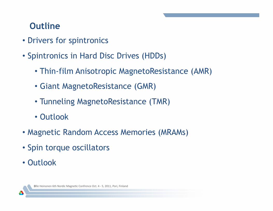
Outline
• Drivers for spintronics
• Spintronics in Hard Disc Drives (HDDs)
• Thin-film Anisotropic MagnetoResistance (AMR)
• Giant MagnetoResistance (GMR)
• Tunneling MagnetoResistance (TMR)
• Outlook
• Magnetic Random Access Memories (MRAMs)
• Spin torque oscillators
• Outlook
Olle Heinonen 6th Nordic Magne5c Confrence Oct. 4 -‐ 5, 2011, Pori, Finland

4
Drivers for spintronics
• Basic physics – magnetotransport, spin-dependent scattering, magnetic heterostructures…(Gruenberg, Fert)
• Physics funding agencies – sometimes novelty-driven so you have to come up with a novelty that will solve the world’s problems
• Semiconductor scaling running out of steam, but still hard to beat…
• Now NAND flash at 19 nm node(!!!!!!), 2 bits/cell, 64 Gbit NAND, 3 bits/cell planned (SanDisk 2011)
• Scaling limit drives new functionalities, 3D architectures
• Semiconductor power consumption
Olle Heinonen 6th Nordic Magne5c Confrence Oct. 4 -‐ 5, 2011, Pori, Finland

5
Drivers for spintronics – power consumption
Olle Heinonen 6th Nordic Magne5c Confrence Oct. 4 -‐ 5, 2011, Pori, Finland

6
Drivers for spintronics – power consumption
Create power-‐efficient electronics. Magne5c spintronics can create devices that do not consume power in off-‐state
Today: slow & large footprint Future: normally “off” electronics
(Sam Bader)
Olle Heinonen 6th Nordic Magne5c Confrence Oct. 4 -‐ 5, 2011, Pori, Finland

7
Areal Density progression in HDDs
Longitudinal Recording
Perpendicular Recording
(Mark Kief, Mark Kryder)
GMR and MTJ
Olle Heinonen 6th Nordic Magne5c Confrence Oct. 4 -‐ 5, 2011, Pori, Finland

8
Spintronics in HDDs
• Basic problem: sense relatively weak (~1000 Oe), spatially localized (~10 nm) fields with high SNR and at high frequencies (~1 GHz)
• Basic drivers:
• Scaling to smaller features, larger areal densities (Gbit/in2) while maintaining SNR
• Power consumption
• Basic idea in thin film heads: use magnetoresistance to sense stray fields from recorded bits in mediaèspin- and charge-currents in sub-micron thin film structures.
Olle Heinonen 6th Nordic Magne5c Confrence Oct. 4 -‐ 5, 2011, Pori, Finland

Bit size and reader technologies
Olle Heinonen 6th Nordic Magne5c Confrence Oct. 4 -‐ 5, 2011, Pori, Finland
9
High MR ra5o translates to High Signal– to–Noise ra5o
10 Gb/in2
20 Gb/in2
40 Gb/in2
100 Gb/in2
32 ktpi x 345 kbpi (794 nm x 74 nm)
45 ktpi x 445 kbpi (564 nm x 57 nm)
75 ktpi x 530 kbpi (339 nm x 48 nm)
167 ktpi x 600 kbpi (152 nm x 39 nm)
1 Terabit/in2 1,000 ktpi x 1,000 kbpi (25.4 nm x 25.4 nm)
200Gb/in2 200 ktpi x 1,000 kbpi (127 nm x 25 nm)
Areal Density vs. Magne5c Bit Sizes

Thin film GMR and AMR heads
Olle Heinonen 6th Nordic Magne5c Confrence Oct. 4 -‐ 5, 2011, Pori, Finland
10
(From Jimmy Zhu)

AMR head advantages
Olle Heinonen 6th Nordic Magne5c Confrence Oct. 4 -‐ 5, 2011, Pori, Finland
11
• Enabled the use thin film deposi5on (pla5ng, spueering) and paeerning
technologies è rapid scaling (reduc5on of feature sizes)
• SNR independent of disc velocity (in contrast with induc5ve heads)
• More complex process technologies
• Mul5-‐layer structures
• Larger materials set (sof magnets, hard magnets, insulators,
conductors)
• Low AMR ra5o ~1% limits SNR with reduced reader size

GMR read heads
Olle Heinonen 6th Nordic Magne5c Confrence Oct. 4 -‐ 5, 2011, Pori, Finland
12
• Much larger magnetoresistance (signal) then in AMR heads – higher SNR while shrinking feature size
• More complicated reader structure, more aeen5on to interface phenomena • More advanced deposi5on (spueering) and paeerning techniques
Sof Magne5c Shield
Sof Magne5c Shield
Al203 Gap
Al203 Gap
Permanent magnet Permanent magnet
Current Lead Current Lead
Ac5ve Sensing Region
13
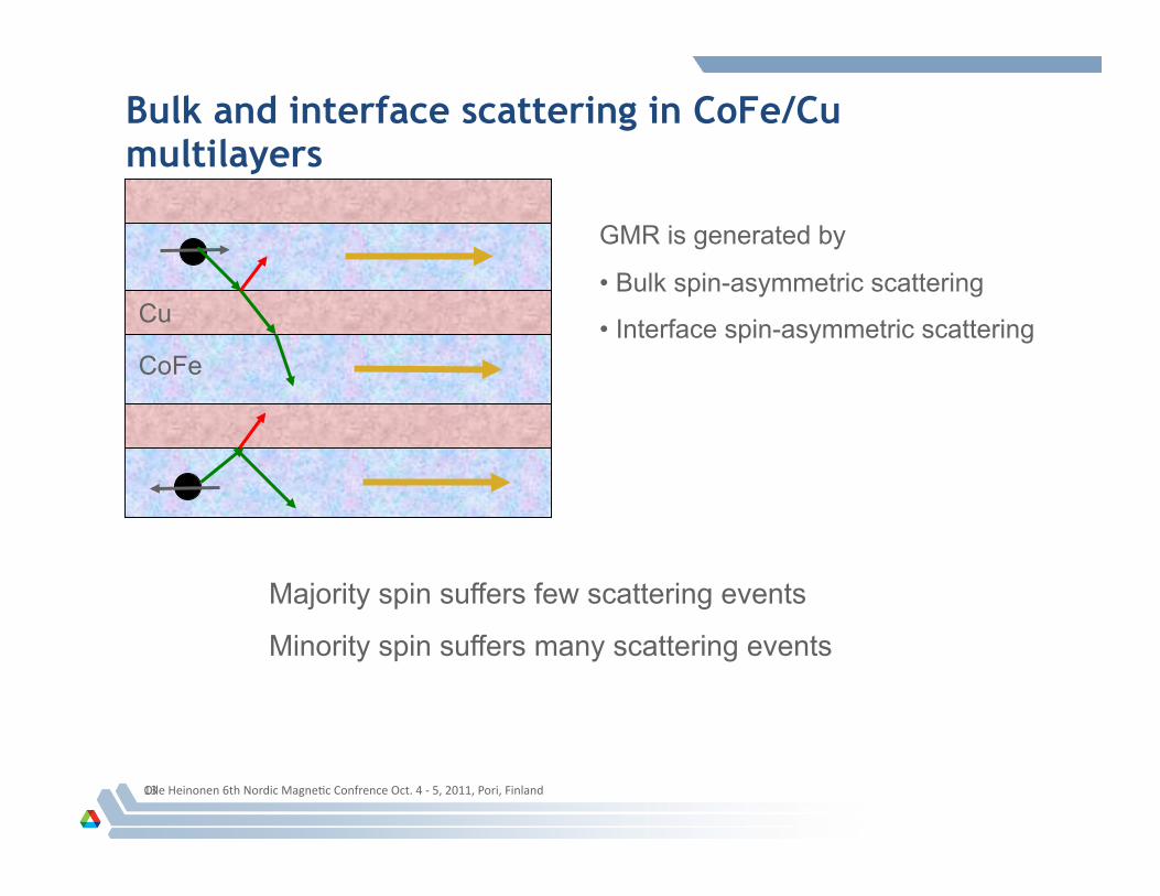
Bulk and interface scattering in CoFe/Cu multilayers
Majority spin suffers few scattering events
Minority spin suffers many scattering events
Cu
CoFe
GMR is generated by
• Bulk spin-asymmetric scattering
• Interface spin-asymmetric scattering
Olle Heinonen 6th Nordic Magne5c Confrence Oct. 4 -‐ 5, 2011, Pori, Finland

14
GMR-effect: band-match and transmission properties at CoFe-Cu interface
• CoFe and Cu in (111) texture have a very good band-match in the majority channel, and a poor band-match in the minority channel
• Majority spins are transmitted relatively easily across the 2D Fermi surface; minority spins are largely reflected
• This leads to a spin-asymmetric interface resistance which contributes (in addition to spin-asymmetric scattering within the CoFe layers) to the GMR resistance
Transmission probabilities for majority and minority electrons incident from CoFe to Cu.
Blue to white colors indicate increasing transmission probablility
W.H. Butler, O. Heinonen and X.-G. Zhang, in Physics of Ultra-High Density Magnetic Recording, J. van Ek, M. L. Plumer, and D. Weller (eds) (Springer 1999))
Olle Heinonen 6th Nordic Magne5c Confrence Oct. 4 -‐ 5, 2011, Pori, Finland
15
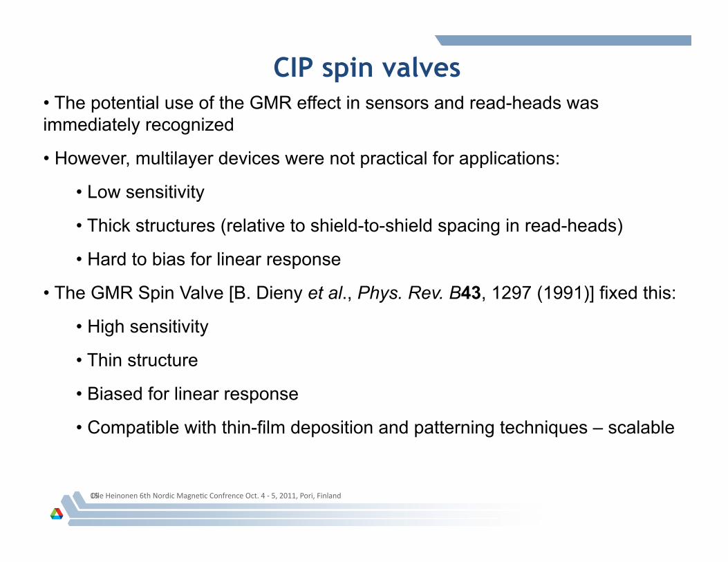
CIP spin valves • The potential use of the GMR effect in sensors and read-heads was immediately recognized
• However, multilayer devices were not practical for applications:
• Low sensitivity
• Thick structures (relative to shield-to-shield spacing in read-heads)
• Hard to bias for linear response
• The GMR Spin Valve [B. Dieny et al., Phys. Rev. B43, 1297 (1991)] fixed this:
• High sensitivity
• Thin structure
• Biased for linear response
• Compatible with thin-film deposition and patterning techniques – scalable
Olle Heinonen 6th Nordic Magne5c Confrence Oct. 4 -‐ 5, 2011, Pori, Finland
16
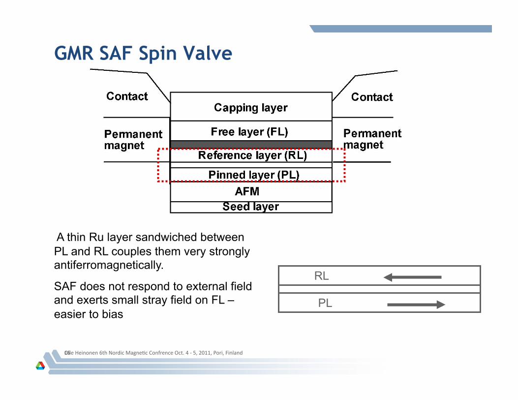
A thin Ru layer sandwiched between PL and RL couples them very strongly antiferromagnetically.
SAF does not respond to external field and exerts small stray field on FL – easier to bias
PL
RL
GMR SAF Spin Valve
Olle Heinonen 6th Nordic Magne5c Confrence Oct. 4 -‐ 5, 2011, Pori, Finland

17
CIP SAF spin valve
Transmission probabilities for majority and minority electrons incident on Ru from CoFe.
Majority spins tend to be reflected, and minority transmitted.
W.H. Butler, O. Heinonen and X.-G. Zhang, in Physics of Ultra-High Density Magnetic Recording, J. van Ek, M. L. Plumer, and D. Weller (eds) (Springer 1999))
• Unexpected bonus for transport and GMR: • Reflection of majority spin electrons incident on Ru from CoFe is beneficial to GMR!
• Ru on CoFe smooths out the surface (reduces “doming”).
Olle Heinonen 6th Nordic Magne5c Confrence Oct. 4 -‐ 5, 2011, Pori, Finland

18
Current density and GMR properties Better interface control, improved Cu, specular cap, and the magic of Ru improve magnetotransport properties
Cu
GMR signal
Free layer Reference layer
Pinned layer
Olle Heinonen 6th Nordic Magne5c Confrence Oct. 4 -‐ 5, 2011, Pori, Finland

19
CIP spin valves – end-of-life
• Highest achievable GMR was around 20%
• Signal voltage limited by maximum current – Joule heating. Signal voltage is
As the device size decreases, heat is dissipated less efficiently from the reader, so the bias current has to be reduced.
• Main limitations to continued scaling for SVs were
• increased heat dissipation
• unfavorable SNR scaling
• insulating layers between SV and shields structures prevented small shield-to-shield spacing
Olle Heinonen 6th Nordic Magne5c Confrence Oct. 4 -‐ 5, 2011, Pori, Finland
20
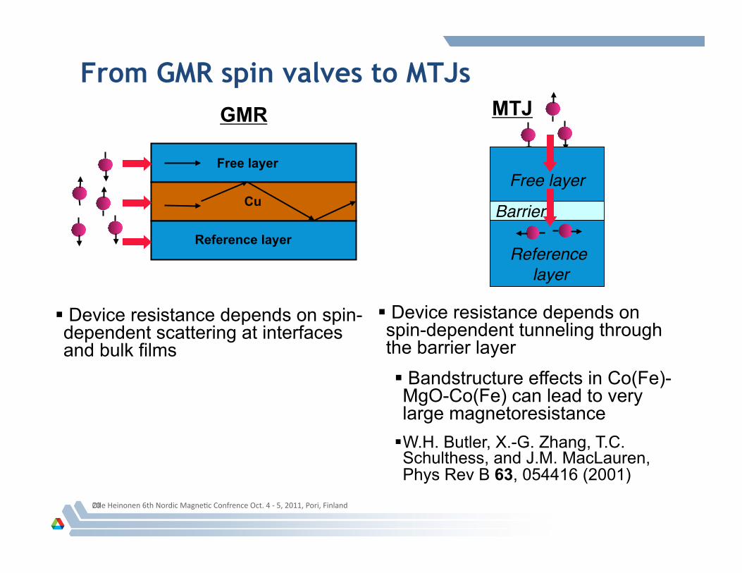
§ Device resistance depends on spin-dependent scattering at interfaces and bulk films
From GMR spin valves to MTJs
Free layer
Cu
Reference layer
Free layer!
Reference layer!
Barrier!
GMR MTJ
§ Device resistance depends on spin-dependent tunneling through the barrier layer § Bandstructure effects in Co(Fe)-MgO-Co(Fe) can lead to very large magnetoresistance
§ W.H. Butler, X.-G. Zhang, T.C. Schulthess, and J.M. MacLauren, Phys Rev B 63, 054416 (2001)
Olle Heinonen 6th Nordic Magne5c Confrence Oct. 4 -‐ 5, 2011, Pori, Finland
21
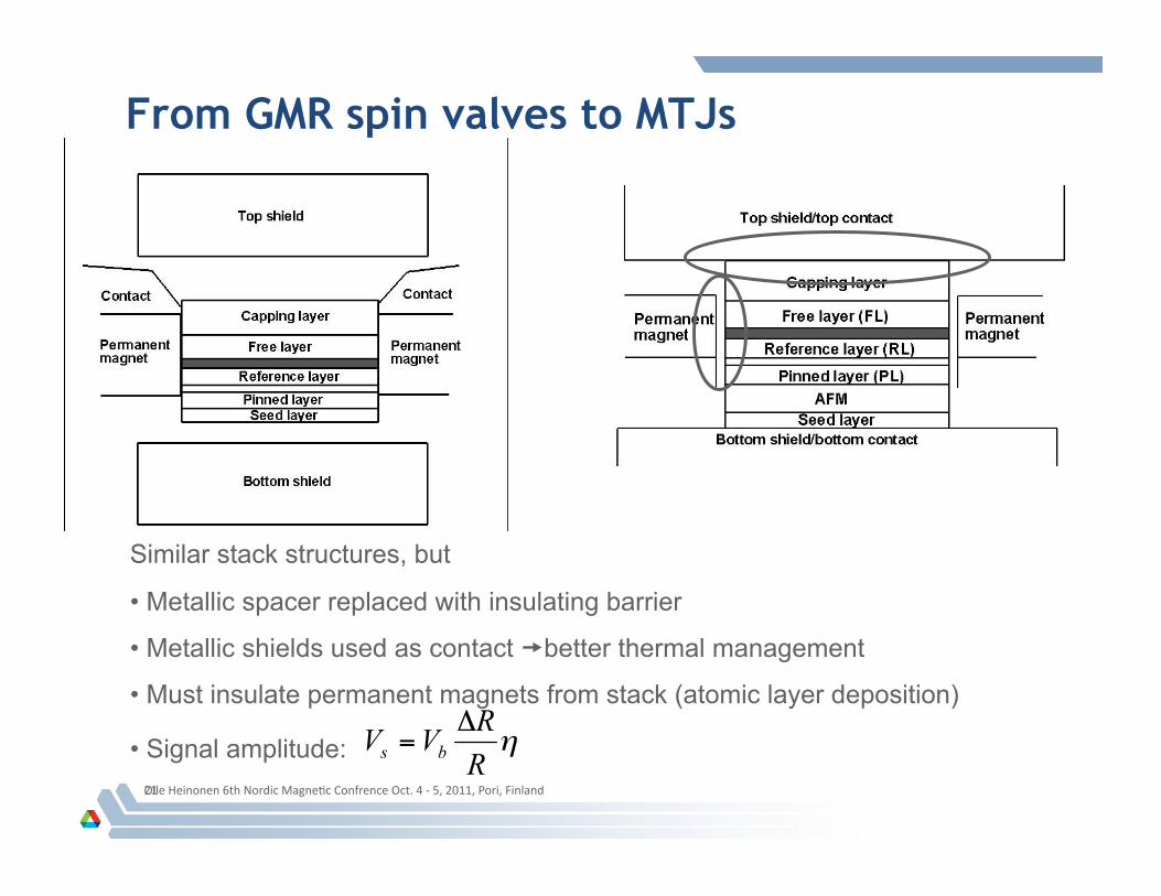
From GMR spin valves to MTJs
Similar stack structures, but
• Metallic spacer replaced with insulating barrier
• Metallic shields used as contact �better thermal management
• Must insulate permanent magnets from stack (atomic layer deposition)
• Signal amplitude: Olle Heinonen 6th Nordic Magne5c Confrence Oct. 4 -‐ 5, 2011, Pori, Finland

22
Tunneling readers – barrier materials • Want:
• High tunneling magnetoresistance (TMR)
• Low resistance-area (RA) product (~1 Ω-µm2)
• Reliable – able to withstand bias voltage during lifetime of reader
• Initial MTJs were based on alumina barriers. Drawbacks:
• Kinetics of alumina formation makes it hard to get a thin (low RA) barrier free of defects (pinholes)
• Metallic Al deposited on CoFe electrode forms an alloy with Co.
Olle Heinonen 6th Nordic Magne5c Confrence Oct. 4 -‐ 5, 2011, Pori, Finland

Early product TMR head (~150 Gbit/in2)
Olle Heinonen 6th Nordic Magne5c Confrence Oct. 4 -‐ 5, 2011, Pori, Finland
23
Free sensing layer
Thin insulating barrier < 1 nm thickness
Antiferromagnet for pinning the fixed layer
§ Abueed junc5on layout with hard bias § Reader width ~ 90-‐100nm and Shield spacing ~ 80nm
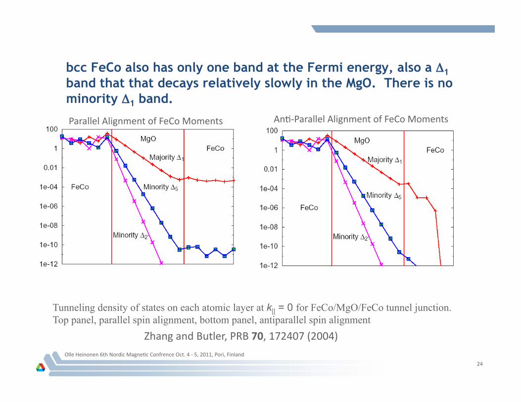
bcc FeCo also has only one band at the Fermi energy, also a Δ1 band that that decays relatively slowly in the MgO. There is no minority Δ1 band.
Tunneling density of states on each atomic layer at k|| = 0 for FeCo/MgO/FeCo tunnel junction. Top panel, parallel spin alignment, bottom panel, antiparallel spin alignment
Parallel Alignment of FeCo Moments An5-‐Parallel Alignment of FeCo Moments
Olle Heinonen 6th Nordic Magne5c Confrence Oct. 4 -‐ 5, 2011, Pori, Finland
24
Zhang and Butler, PRB 70, 172407 (2004)

MTJ in HDDs – present status and end-of-life
§ Currently in produc5on RA≈0.5 Ω(μm)2 and TMR≈100% § Reader dimensions < 50 nm x 50 nm § Difficult to make narrower (for higher track density) and
thinner (for higher linear density) while maintaining stability, amplitude (SNR), and reliability
Olle Heinonen 6th Nordic Magne5c Confrence Oct. 4 -‐ 5, 2011, Pori, Finland
25
Page 26
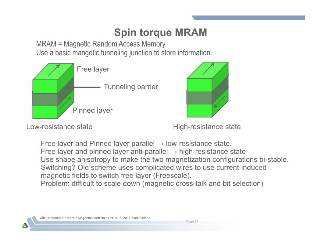
Spin torque MRAM MRAM = Magnetic Random Access Memory Use a basic mangetic tunneling junction to store information.
Pinned layer
Free layer
Tunneling barrier
Free layer and Pinned layer parallel → low-resistance state. Free layer and pinned layer anti-parallel → high-resistance state Use shape anisotropy to make the two magnetization configurations bi-stable. Switching? Old scheme uses complicated wires to use current-induced magnetic fields to switch free layer (Freescale). Problem: difficult to scale down (magnetic cross-talk and bit selection)
© Seagate 2009
Low-resistance state High-resistance state
Olle Heinonen 6th Nordic Magne5c Confrence Oct. 4 -‐ 5, 2011, Pori, Finland

Spin torque • A spin-‐polarized current exerts a torque on the magne5za5on in a thin magne5c film
Current direc5on
Electron flow direc5on
Current direc5on
Electron flow direc5on
Back-‐scaeered electrons an5-‐parallel to the magne5za5on in 2 exert a torque on 1
Transmieed electrons parallel to the magne5za5on direc5on in 1 exert a torque on 2
1 2
1 2
27
Olle Heinonen 6th Nordic Magne5c Confrence Oct. 4 -‐ 5, 2011, Pori, Finland

Page 28
Perpendicular-anisotropy (PA) spin-torque RAM
Low-‐energy direc5ons High-‐energy direc5ons
In in-‐plane STRAM the direc5on of the Free layer magne5za5on is determined by the shape
In PA STRAM, the direc5on of the Free layer magne5za5on is determined by intrinsic magne5c anisotropy. This offers advantages over in-‐plane STRAM:
• The thermal stability is insensi5ve to shape and process varia5ons
• Can easily make circles down to ~65 nm diameter with 193 nm stepper
• The switching current is reduced
The thermal stability is determined by the energy difference between high-‐ and low-‐energy direc5ons and depends on the shape. This make the thermal stability sensi5ve to process varia5ons. Difficult to make small ellipses (~1:2 aspect ra5o) small axis 65 nm or smaller with 193 nm stepper.
Free layer
Reference layer
Olle Heinonen 6th Nordic Magne5c Confrence Oct. 4 -‐ 5, 2011, Pori, Finland

Page 29
In-plane elliptical spin torque magnetic random access memory structure
SEM image of nominally 90 nm x 180 nm STRAM – note edge roughness, or “wobbliness”
Olle Heinonen 6th Nordic Magne5c Confrence Oct. 4 -‐ 5, 2011, Pori, Finland

Olle Heinonen 6th Nordic Magne5c Confrence Oct. 4 -‐ 5, 2011, Pori, Finland
30
Perpendicular-anisotropy spin-torque MRAM
Advantages: • Decouple thermal stability (energy barrier) from processing condi5ons • Reduced cri5cal current density for switching – but reduced write current can lead to read disturbances… Remaining issues: • Materials science: must integrate magne5c layers with perpendicular anisotropy while maintaining high-‐TMR CoFe/MgO/CoFe interface with (001) texture. Thin (very thin, ~1 nm) CoFeB has perpendicular anisotropy (Ohno) • Must maintain low cri5cal current density – reliability as well as size of selec5on transistor • Recent developments perpendicular spin-‐torque MRAM (Tohoku U – NEC): Sato et al, APL 2011

Olle Heinonen 6th Nordic Magne5c Confrence Oct. 4 -‐ 5, 2011, Pori, Finland
31
1T-‐1R 64 bit x 128 word using 140 nm CMOS processing Perpendicular-‐anisotropy CoFeB/MgO/CoFeB
Design and Fabrication of a One-Transistor/One-Resistor Nonvolatile Binary
Content-Addressable Memory Using Perpendicular Magnetic Tunnel Junction Devices
with a Fine-Grained Power-Gating Scheme
Shoun Matsunaga, Masanori Natsui1, Shoji Ikeda2, Katsuya Miura2;3,Tetsuo Endoh4, Hideo Ohno2, and Takahiro Hanyu1!
Center for Spintronics Integrated Systems (CSIS), Tohoku University, Sendai 980-8577, Japan1Laboratory for Brainware Systems, Research Institute of Electrical Communication, Tohoku University, Sendai 980-8577, Japan2Laboratory for Nanoelectronics and Spintronics, Research Institute of Electrical Communication, Tohoku University, Sendai 980-8577, Japan3Hitachi Advanced Research Laboratory, Kokubunji, Tokyo 185-8601, Japan4Center for Interdisciplinary Research, Tohoku University, Sendai 980-8578, Japan
Received February 24, 2011; accepted March 24, 2011; published online June 20, 2011
A perpendicular magnetic tunnel junction (P-MTJ)-based one-transistor/one-resistor (1T–1R) binary content-addressable memory (CAM) is
proposed for a high-density nonvolatile CAM. The proposed CAM cell performs an equality-search operation between an input bit and thecorresponding stored bit by detecting the difference of a ‘‘cell resistance’’, where the cell resistance is determined by the series connection of one
metal–oxide–semiconductor (MOS) transistor and one P-MTJ device. This circuit structure makes it possible to implement a compact nonvolatile
CAM cell circuit with 1.25 !m2 of a cell size in a 0.14 !m complementary MOS (CMOS)/P-MTJ process. Moreover, the equality-search operation
in a bit-serial fashion is used for great reduction of the activity rate in the proposed CAM cell array, since most of the mismatched words in theCAM are detected by just several higher bits of comparison results in the word circuits. By applying a bit-level fine-grained power gating scheme, a
fabricated 64-bit ! 128-word nonvolatile CAM achieves high density with maintaining low search energy under 3.1% of activity rate in the cell
array. # 2011 The Japan Society of Applied Physics
1. Introduction
A content-addressable memory (CAM) is a powerful data-searching hardware with a parallel data processing cap-ability. It can be used for a number of applications suchas parallel image processors, data compression hardware,and central processing unit (CPU) caches.1–6) However, aconventional complementary metal–oxide–semiconductor(CMOS)-based CAM tends to su!er from an area penaltysince it must consist of a normal static random accessmemory (SRAM) cell (six transistors) to perform datastorage function and additional logic circuit (three transistorsat least) to perform equality-search operation.7) Moreover,standby power dissipation due to leakage current in aCMOS-based cell circuit is increasingly dominating itspower dissipation in recent nanometer-scaled technol-ogy.8–12)
One possible solution to realize a high-density and low-standby-power CAM is to use metal–oxide–semiconductor(MOS)/nonvolatile-device-hybrid logic-in-memory circui-try, where nonvolatile storage elements are distributed andstacked over a logic-circuit plane,13–21) and to cut o! thepower supply to inactive circuit blocks whenever they arein standby mode (power gating).22,23) In order to fully takeadvantages of the logic-in-memory circuitry, it is importantto implement a nonvolatile device that has superiorcapabilities such as shorter access time, unlimited endur-ance, scalable write, and small dimension comparable to theemployed CMOS technology. The only available candidateof a nonvolatile storage device that can satisfy all the aboverequirements at present is the one using spin-transfer-torque(STT) magnetic tunnel junction (MTJ) devices.24) Inparticular, a newly-developed MTJ device which uses largeperpendicular magnetic anisotropy at the interface betweenan insulator and magnetic electrode, called perpendicularMTJ (P-MTJ) device, is expected to provide a great
advantage to achieve ultra-low power consumption in verylarge scale integrated circuits (VLSIs).25)
In this paper, we propose a nonvolatile bit-serial binaryCAM using P-MTJ-based fine-grained power-gatingscheme, and demonstrate its operating mechanism witha fabricated 64-bit " 128-word CAM chip in a 0.14 !mCMOS/P-MTJ process. Since a P-MTJ device is used as notonly a nonvolatile storage element but also a logic-operationelement, one-transistor/one-resistor (1T–1R)-style compactCAM cell circuit is implemented. Moreover, a combinationof bit-level equality-search scheme and a fine-grainedpower-gating scheme which is achieved by the nonvolatilestorage capability of MTJ devices decreases the cell activityrate to 3.1%, which further reduces power dissipation of thecircuit. As the result, an ultra-low-power bit-serial CAMwhich eliminates most of the wasted standby power can beobtained.
2. MOS/MTJ-Hybrid 1T–1R Binary CAM Cell withThree-State Combined Resistance
Figure 1 shows a P-MTJ-based CAM cell structure anda measured resistance versus current (R–I) characteristic ofthe fabricated P-MTJ device. The proposed CAM cellconsists of one transistor and one P-MTJ device. The CAMcell is designed and fabricated by using two-finger layoutwhich is the same as that of a standard magnetic randomaccess memory (MRAM) cell array with a 1T–1R structure.The P-MTJ device, whose shape is 100 nm! circular, isstacked over the MOS and metal layers with its upper andlower electrodes.
The most important advantage of the P-MTJ device overconventional in-plane STT MTJ device26) is its lower writecurrent. However the lower write current may causeunexpected spin inversion of the MTJ device during readoperation (read disturbance). To avoid this, it is important todetermine the current direction at read (equality-search)operation in the CAM by considering an asymmetric shapeof the R–I characteristic of P-MTJ device as shown in!E-mail address: [email protected]
Japanese Journal of Applied Physics 50 (2011) 063004
063004-1 # 2011 The Japan Society of Applied Physics
REGULAR PAPERDOI: 10.1143/JJAP.50.063004

Olle Heinonen 6th Nordic Magne5c Confrence Oct. 4 -‐ 5, 2011, Pori, Finland
32
Spin-torque oscillators
• New physics coupling DC currents with magne5za5on dynamics
• Spin torque oscillators – very high Q-‐values in nanoscale GHz oscillators
Nazarov, Nikolaev, Gao, Cho, and Song – MgO MTJ (MMM-‐2007)

Magnetization dynamics – Landau-Lifshitz-Gilbert equation
33
Olle Heinonen 6th Nordic Magne5c Confrence Oct. 4 -‐ 5, 2011, Pori, Finland
!
d ˆ m dt
= "# e ˆ m $! H eff[ ] " # e %
1+% 2 ˆ m $ ˆ m $! H eff( )[ ]
Precession (conserva5ve torque)
Dissipa5on (non-‐conserva5ve torque)
!
! H eff
!
ˆ m Magne5za5on precesses around the effec5ve field. The dissipa5ve torque brings the magne5za5on parallel to the effec5ve field.
!
ˆ m =!
M !
M α = dimensionless damping constant

Add “Slonczewski spin torque”:
34
Olle Heinonen 6th Nordic Magne5c Confrence Oct. 4 -‐ 5, 2011, Pori, Finland
!
! H eff || ˆ m RL
!
ˆ m
Depending on the sign of the current, the spin torque term adds dissipa5on, or pumps energy into the system è can have undamped oscilla5on! Large spin torque can make magne5za5on switch (Ka5ne et al, PRL 2000)
!
! " = # e aJ ˆ m FL $ ˆ m FL $ ˆ m RL( )[ ],
!
aJ "#jPMSt
aJ=effec5ve field due to spin torque j= current density P=spin polariza5on MS=magne5za5on density t= FL thickness

STOs
35
Olle Heinonen 6th Nordic Magne5c Confrence Oct. 4 -‐ 5, 2011, Pori, Finland
• Metallic nano-‐contacts or MgO MTJs • MTJs provide large signal, but worse tunability • Couple oscillators for larger output • Sub-‐micron sized GHz oscillator driven by dc currents(!) with frequencies up to tens of GHz; readily integrated with Si-‐CMOS using back-‐end-‐of-‐line processing.
Issues • Synchroniza5on of many oscillators • Frequency range for MgO STOs • Amplitude for nano-‐contact STOs • Ul5mate coherence limit:
• Temperature-‐driven decoherence • Mode-‐hopping driven decoherence

36
Back-ups
Olle Heinonen 6th Nordic Magne5c Confrence Oct. 4 -‐ 5, 2011, Pori, Finland