Embed Size (px)
Citation preview

ENSC 460: Special Topics: Theory, Analysis, and Simulation
of Nonlinear Circuits Final Project Presentation
Spring 2004
SPICE and MATLAB Simulation on Nonlinear Circuits
Alan Chuang 200034805 Wayne Huang 200036132
Henry Lin 200036321

2
Table of Contents Table of Contents ................................................................................................................ 2 List of Figures ..................................................................................................................... 3 List of Tables....................................................................................................................... 3 1 Abstract ....................................................................................................................... 4 2 Introduction ................................................................................................................. 4 3 Background ................................................................................................................. 5
3.1 Model and Constants Employed ......................................................................... 5 3.2 Theories............................................................................................................... 6
4 Results ......................................................................................................................... 9 4.1 Circuit 1 - Flip-Flop ............................................................................................ 9 4.2 Circuit 2............................................................................................................. 11 4.3 Circuit 3............................................................................................................. 15 4.4 Circuit 4 – Orchard............................................................................................ 16 4.5 Circuit 5 - Schmitt Trigger ................................................................................ 21
5 Discussion ................................................................................................................. 25 6 Conclusion................................................................................................................. 27 7 References ................................................................................................................. 28 8 Appendix ................................................................................................................... 29
8.1 Circuit 1 – Flip Flop .......................................................................................... 29 8.2 Circuit 2............................................................................................................. 31 8.3 Circuit 3............................................................................................................. 33 8.4 Circuit 4 – Orchard............................................................................................ 36 8.5 Circuit 5 – Schmitt Trigger ............................................................................... 38

3
List of Figures Figure 3-1. Ebers-Moll Model. ........................................................................................... 5 Figure 4-1: Flip-Flop Circuit with Auxiliary Source .......................................................... 9 Figure 4-2: i-v Characteristic of Flip-Flop Circuit with Auxiliary Source ....................... 10 Figure 4-3: Original Flip-Flop Circuit .............................................................................. 10 Figure 4-4: Circuit Diagram of Circuit 2 and Its Feedback Paths..................................... 11 Figure 4-5: v-i Characteristic of Circuit 2 ......................................................................... 12 Figure 4-6: i-v Characteristic (S-type NDR) of Circuit 2.................................................. 12 Figure 4-7: v-i Characteristic of Circuit 2 (R1 = 11k, R2 = 3k, R3 = 2k)......................... 13 Figure 4-8: i-v Characteristic (S-type NDR) of Circuit 2 (R1 = 11k, R2 = 3k, R3 =2k) .. 13 Figure 4-9: i-v Characteristic (Set 1) of Circuit 2 When Current Driven ......................... 14 Figure 4-10: i-v Characteristic (Set 2) of Circuit 2 When Current Driven ....................... 14 Figure 4-11; Circuit Diagram of Circuit 3 and Feedback Paths........................................ 15 Figure 4-12: i-v Characteristic of Circuit 3 (R1 = 2.2k, R2 = 470, R3 = 10k).................. 15 Figure 4-13: Orchard Circuit When (a) Voltage Driven, and (b) Current Driven ............ 16 Figure 4-14: i-v Characteristic of Current Driven Orchard Circuit................................... 17 Figure 4-15: i-v Characteristic of Current Driven Orchard Circuit .................................. 18 Figure 4-16: Voltage Driven Orchard Circuit with Q2 Changed to npn and Flipped....... 19 Figure 4-17: i-v Characteristic for the Altered Voltage Driven Orchard Circuit.............. 19 Figure 4-18: Zoom-in Version of the Lower Portion of Figure 4-17................................ 20 Figure 4-19: Experimental Result for the Current Driven Orchard Circuit ...................... 20 Figure 4-20: Schmitt Trigger and Feedback Structure...................................................... 21 Figure 4-21: i-v Characteristic for the Schmitt Trigger..................................................... 22 Figure 4-22: Actual Circuit Built to Investigate the Schmitt Trigger Behavior................ 23 Figure 4-23: (a) experimental v-i characteristic (b) simulation result............................ 24 Figure 4-24: Voltages at node Iout (ch 1) and the base of Q1 (ch 2) in time domain ......... 24 Figure 5-1:Vout v.s. Vin Relation of Schmitt Trigger. ..................................................... 25 Figure 5-2: Vout v.s. Vin Relation of Schmitt Trigger, PSPICE Simulation ...................... 26 Figure 5-3: Vin v.s. Iout Relation for Schmitt Trigger with Wilson Current Source .......... 26
List of Tables Table 4-1: Comparison Table of PSPICE and Matlab of Flip-Flop Circuit...................... 11 Table 4-2: Comparison between PSPICE and Matlab for Circuit 2 ................................. 14 Table 4-3: Comparison Table of PSPICE and Matlab of Circuit 3................................... 16 Table 4-4: Comparison Table of PSPICE and Matlab for Orchard Circuit ...................... 18 Table 4-5: Comparison Table of PSPICE and Matlab for Schmitt Trigger ...................... 22

4
1 Abstract We attempted to verify the validity of PSPICE simulation and mathematical analysis with Ebers-Moll model by comparing their results for five different circuits which display negative differential resistance (NDR) and multiple operating point (MOP) characteristics. In some cases, we also constructed the actual circuits and used them as references to ascertain the accuracy of the results generated via simulation and numerical analysis. Through these investigations, we have successfully shown that both SPICE and the Ebers-Moll model are in general accurate at predicting the behavior of circuits with NDR’s.
2 Introduction Circuits with negative resistances and multiple operating points are useful in applications such as negative resistors and memory cells. However, because of their abnormal behavior, their dc operating points and general behavior are usually hard to predict. In this project, we experimented on five circuits and all of which have NDR behavior, including Schmitt Trigger, Orchard circuit, flip-flop, and two other circuits. We applied theorems from the papers and utilized them as tools to help us predict the circuits’ behavior, focusing mainly on their operating points and NDR regions, and simulated these circuits with PSPICE and MATLAB in search for their multiple operating points. For the Schmitt Trigger and the Orchard circuit, we implemented the actual circuits and observed the experimental results on an oscilloscope. The following sections describe the applied theorems, the experimental procedure, and the outcomes of our investigation.

5
3 Background The simulations in this project were carried out in PSPICE and MATLAB. In this section, we will introduce the models and constants used in both simulation approaches, as well as the theories used behind our analysis.
3.1 Model and Constants Employed The circuit components investigated in our project include both npn and pnp bipolar junction transistors. For PSPICE simulation, the models used are 2N3904 and 2N3906 for the npn and pnp BJT’s, respectively. As for the mathematical analysis implemented with MATLAB, we applied Ebers-Moll model, shown in Figure 1, in substitution for the transistors.
Figure 3-1. Ebers-Moll Model.
In Figure 3.1, the values of ie and ic depends on v1 an v2 with the following relationships:
)1( /1 −= kTqvee emi (3.1.1)
)1( /2 −= kTqvcc emi
(3.1.2)
6
where k is the Boltzmann’s constant, T =300K is the room temperature in Kelvin, and me and mc are the emitter and collector saturation current, respectively. From PSPICE model parameters, the emitter and collector saturation current, for npn and pnp transistor, respectively, are: 6.734E-15A, 15.833E-15A, 1.41E-15A, and 1.684E-15A.
3.2 Theories Given a transistor circuit, we are often interested in finding the existence and uniqueness of the operating point of the circuit. For the five circuits we have investigated, we applied theories from the papers to characterize their behavior. A circuit’s ability to possess multiple operating points depends on four factors: circuit topology, circuit parameters, biasing, and transistor types. For our project, our focus is on two-transistor circuits, Theorem 7 in [3] states that a two-transistor circuit, with arbitrary number of transistors and independent sources, possesses at most three dc operating points. Following sections discuss these factors for two-transistor circuits. Topology Theorem 7 in [3] states that a two-transistor circuit, with an arbitrary number of resistors and independent sources, possesses at most three dc operating points. We know that a transistor circuit can possess multiple operating points only if it possesses a feedback structure [3]; that is, having the right topology is a necessary condition for having multiple operating points. We are also interested in if the circuit exhibits negative differential resistance (NDR) behavior. It is shown that for a one-port, an N-type NDR can occur only if a feedback structure is present when the port is open-circuited and an S-type NDR can occur only if a feedback structure is present when the port is short-circuited [1, 2]. In other words, topology acts as our first check condition for a circuit possessing multiple operating points or NDR. If the circuit does not have a feedback structure, we can conclude right away that the circuit can have at most one operating point. Parameters We can always write the equation for a transistor circuit as
A*F(v) + B*v + c = 0 (3.1)
The problem of identifying the existence of NDR is equivalent to identify if (A,B) is a Wo pair. The sign of determinant det(AD+B) is an important indicator for possible NDR behavior in transistor circuits [1], where matrices A and B model the resistive part of the circuit and the presence of nonlinear elements in the circuit, and D is a diagonal matrix. Any transistor one-port, when biased at an operating point where NDR is exhibited, will necessarily be operating at a point where det(AD+B) < 0.
7
det(AD + B) = c1234d1d2d3d4 + c1234d1d2d3d4 + c123d1d2d3 + c124d1d2d4 + c134d1d3d4 + c234d2d3d4 + c12d1d2 + c13d1d3+ c14d1d4 + c23d2d3+ c24d2d4 + c34d3d4 + c1d1+ c2d2 + c3d3 + c4d4+ c0 (3.2)
cs , with s denoting a set of integers, is the determinant associated with a matrix from the set C(A,B) obtained by taking columns s from matrix A, and the rest of the columns from matrix B, while their original relative order is maintained. It has been proved that in a two-transistor case, only one of the c13, c14, c23, c24 can possibly be negative [3]. If we also know the feedback structure, then we can be sure which one of the 4 coefficients is possibly negative. If G matrix exists for a circuit, we can write the equation as
F(v) + T-1G*v + T-1G *c = 0 (3.3) The problem of identifying the existence of NDR is equivalent to identify if T-1G is a Po matrix. In other words, if we can choose circuit parameters (e.g. resistor values) such that det(T-1G) < 0, the circuit can possibly exhibit NDR. It has been proved that in a two-transistor circuit, instead of having to evaluate 15 ( 24 – 1 ) principal minors of the matrix T-1G or the matrix composed of ℓ(QT,P), we need only check 4 2x2 principal minors; that is, c13, c14, c23, c24. If we also know the feedback structure, then we can be sure which one of the 4 coefficients is possibly negative. Biasing In addition to having a right topology and choosing circuit parameters to satisfy the determinant condition, there is another important condition, which is related to the physical operation of transistors. That is, the transistors have to be properly biased to forward or reverse state. Biasing Theorem [1] says that for any two-transistor one-port which exhibits NDR behavior, when the one-port is operating at any point on the region of NDR, no transistor can be in the off state, and if the emitter (collector) is involved in the feedback structure, the corresponding transistor must be in the forward (reverse) state. Also, it is shown that a two-transistor one-port, with common-emitter feedback structure, can exhibit NDR only if the transistor junctions are biased such that v1 > v2 (v1 < v2) and v3 > v4 (v3 < v4) for a pnp (an npn) transistor [3]. Consequently, current flows out of the collector of each pnp transistor and into the collector of each npn transistor. These theorems act as a tool to help us bias the transistor junctions so that they physically function properly. Transistor Types Besides these three factors, Chua have conjecture that a one-port containing only resistors and two transistors, no internal sources, can exhibit N-type (S-type) NDR behavior only if the transistors are of similar (complementary) type [2, 3]. Applying this to our example circuits, along with the topology factor, means that if the circuit has a feedback structure

8
when it is voltage (current) driven, its i-v characteristic is expected to be S-type (N-type), and the two transistors must be of complementary (similar) type.

9
4 Results
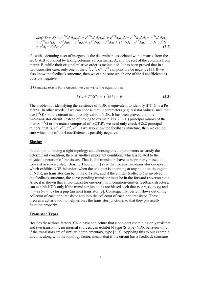
4.1 Circuit 1 - Flip-Flop Illustrated in Figure 4-1 is the circuit diagram of the Flip-Flop circuit with voltage driven feedback path. As shown from the diagram, flip-flop circuit is consisted of two similar types of transistors and it has a feedback path, therefore, we can conclude that it can possess multiple operating points. The two sources shown in the circuit is the internal sources of the circuit, so we cannot utilize it to obtain port characteristics of the circuit. Instead we use an auxiliary source V4 as a tool to ascertain three initial points to assist us in obtaining the actual operating points. Figure 4-2 represents the ICQ1 vs. V4 relationship.
Figure 4-1: Flip-Flop Circuit with Auxiliary Source
10
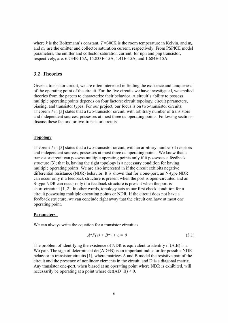
Figure 4-2: i-v Characteristic of Flip-Flop Circuit with Auxiliary Source
Choosing a current value between 0 to -10 uA and drawing a horizontal line across the graph to obtain three intersecting points, we can find three sets of corresponding voltage values for three different operating points. We then use these values acquired as initial guess points to simulate the real circuit in PSPICE. Figure 4-3 illustrates the original circuit with initial guess values applied on certain nodes.
Figure 4-3: Original Flip-Flop Circuit

11
The circuit is also simulated with MATLAB. Since it possesses a feedback structure FS (1,3), we expect the determinant c13 to be negative if the circuit is to exhibit NDR characteristics. And we found the value of the determinant c13 to be -1.3752 x 10⁻¹⁰, which is indeed negative. As previously mentioned the determinant condition is a necessary condition for a circuit to have multiple operating points and it is satisfied here. Comparison between simulation results from Matlab and PSPICE is shown in Table 4-1. We can see that the two sets of values are reasonably close, which is as expected.
Table 4-1: Comparison Table of PSPICE and Matlab of Flip-Flop Circuit
V1 (V) V2 (V) V3 (V) V4 (V) 1 -0.695 -0.617 -0.102 7.42 2 -0.692 0.305 -0.683 0.43
PSPICE
3 -0.088 11.92 -12.05 -11.96 1 -0.714 0.618 -0.096 7.45 2 -0.710 0.318 -0.698 0.407
MATLAB
3 -0.088 11.92 -12.05 -11.96
4.2 Circuit 2 Illustrated below is the circuit diagram of the Circuit 2 with both current driven and voltage driven feedback path shown.
Figure 4-4: Circuit Diagram of Circuit 2 and Its Feedback Paths
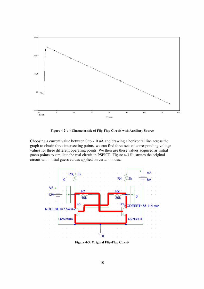
As can be seen, the circuit has two complimentary circuits; therefore, the circuit does not possess N-type NDR, but could possess S-type NDR. Figure 4-5 shows the v-i curve of the circuit. Although this circuit is voltage driven, the simulation is done through replacing the voltage source with a current source and sweeping the current source to ascertain the port characteristic.
12
Figure 4-5: v-i Characteristic of Circuit 2
We can see that for voltages between 1V to 2.2V there could be up to 3 corresponding current values, i.e., when the circuit is voltage driven, it could possess up to 3 operating points. NDR occurs at the range between 5mA to 60mA. Shown in Figure 4-6 is the same relation with x- and y-axis swapped to show the S-type NDR behavior. The NDR region is about 1.2V.
Figure 4-6: i-v Characteristic (S-type NDR) of Circuit 2
We also chose another set of resistor values which satisfies the determinant criteria; the following figures illustrate the corresponding port characteristics. Again, Figure 4-8 is just Figure 4-7 with x- and y-axis swapped, to show the S-type NDR behavior.
13
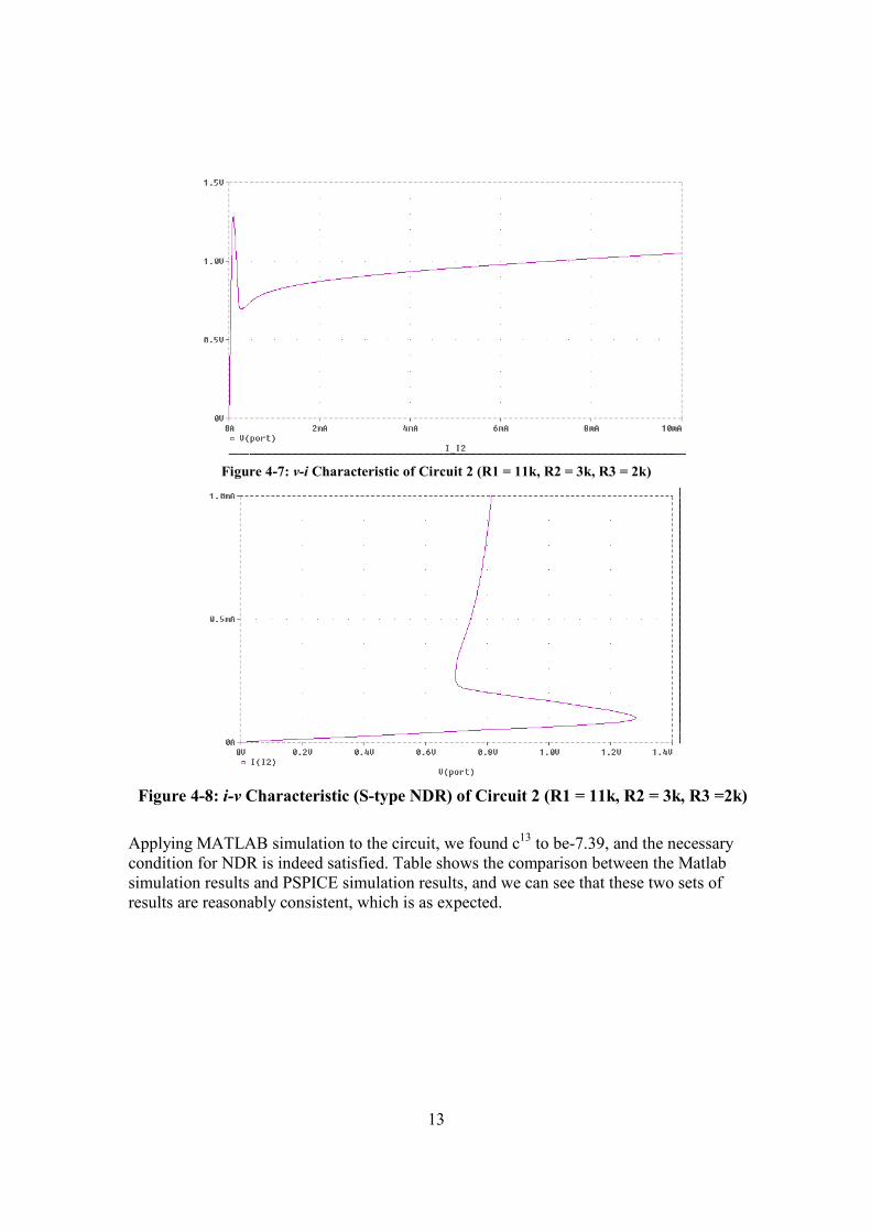
Figure 4-7: v-i Characteristic of Circuit 2 (R1 = 11k, R2 = 3k, R3 = 2k)
Figure 4-8: i-v Characteristic (S-type NDR) of Circuit 2 (R1 = 11k, R2 = 3k, R3 =2k)
Applying MATLAB simulation to the circuit, we found c13 to be-7.39, and the necessary condition for NDR is indeed satisfied. Table shows the comparison between the Matlab simulation results and PSPICE simulation results, and we can see that these two sets of results are reasonably consistent, which is as expected.

14
Table 4-2: Comparison between PSPICE and Matlab for Circuit 2 V1 (V) V2 (V) V3 (V) V4 (V)
1 -0.275 0.387 0.389 -0.707 2 -0.647 -0.371 0.826 0.239
PSPICE
3 -0.716 -0.527 0.911 0.645 1 -0.275 0.366 0.458 -0.641 2 -0.632 -0.340 0.807 0.187
MATLAB
3 -0.758 -0.514 0.855 0.839 To verify that the circuit does not possess N-type NDR when it is voltage driven, we experimented PSPICE simulation and concluded that for these two sets of values, even though the determinant condition is satisfied and the circuit has a feedback structure, we still would not be able to bias the transistors so that this circuit possesses an N-type NDR. As a matter of fact, we have tried a several different combinations (that satisfy the determinant condition, of course), and none of them would achieve an N-type NDR. Figure 4-9 and Figure 4-10 shows the general characteristics when the circuit is current driven.
V_V1
0V 1V 2V 3V 4V 5V 6V 7V 8V 9V 10V-I(V1)
0A
0.5A
1.0A
Figure 4-9: i-v Characteristic (Set 1) of Circuit 2 When Current Driven
V_V1
0V 1V 2V 3V 4V 5V 6V 7V 8V 9V 10V- I(V1)
0A
100mA
200mA
300mA
Figure 4-10: i-v Characteristic (Set 2) of Circuit 2 When Current Driven
15
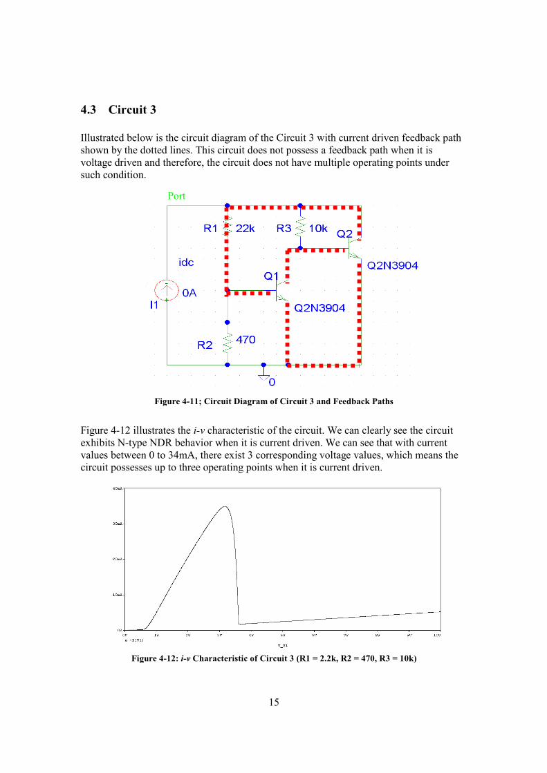
4.3 Circuit 3 Illustrated below is the circuit diagram of the Circuit 3 with current driven feedback path shown by the dotted lines. This circuit does not possess a feedback path when it is voltage driven and therefore, the circuit does not have multiple operating points under such condition.
Figure 4-11; Circuit Diagram of Circuit 3 and Feedback Paths
Figure 4-12 illustrates the i-v characteristic of the circuit. We can clearly see the circuit exhibits N-type NDR behavior when it is current driven. We can see that with current values between 0 to 34mA, there exist 3 corresponding voltage values, which means the circuit possesses up to three operating points when it is current driven.
Figure 4-12: i-v Characteristic of Circuit 3 (R1 = 2.2k, R2 = 470, R3 = 10k)
Port
16
Through MATLAB simulation, we found c13 to be -0.0004525 < 0, and Table 4-3 shows the comparison between the Matlab simulation results and PSPICE simulation results, and we can see that the two sets of results are reasonably consistent.
Table 4-3: Comparison Table of PSPICE and Matlab of Circuit 3
V1 (V) V2 (V) V3 (V) V4 (V)
1 -0.224 0.5 -0.725 0.545 2 -0.627 0.0856 -0.728 2.838
PSPICE
3 -0.790 -0.759 -0.03 17.21 1 -0.165 0.558 -0.723 0.212 2 -0.632 0.0864 -0.719 2.875
MATLAB
3 -0.731 -0.704 -0.0262 17.168
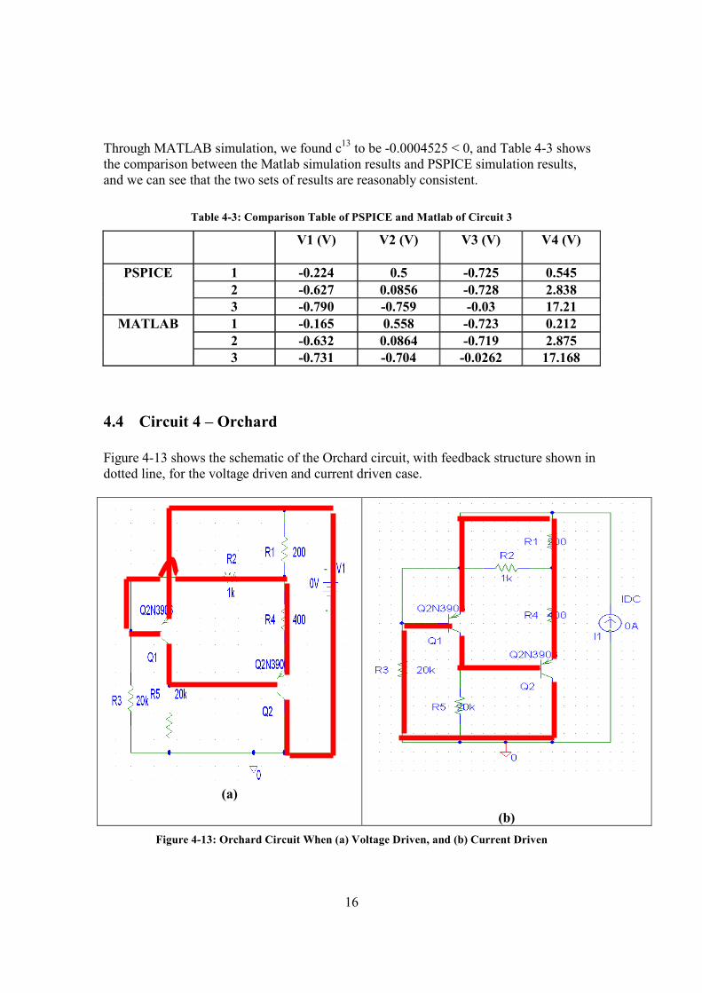
4.4 Circuit 4 – Orchard Figure 4-13 shows the schematic of the Orchard circuit, with feedback structure shown in dotted line, for the voltage driven and current driven case.
(a)
(b) Figure 4-13: Orchard Circuit When (a) Voltage Driven, and (b) Current Driven
17
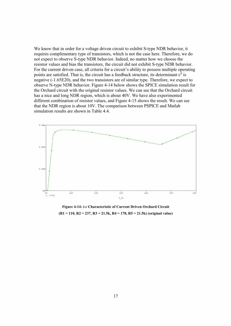
We know that in order for a voltage driven circuit to exhibit S-type NDR behavior, it requires complimentary type of transistors, which is not the case here. Therefore, we do not expect to observe S-type NDR behavior. Indeed, no matter how we choose the resistor values and bias the transistors, the circuit did not exhibit S-type NDR behavior. For the current driven case, all criteria for a circuit’s ability to possess multiple operating points are satisfied. That is, the circuit has a feedback structure, its determinant cij is negative (-1.65E20), and the two transistors are of similar type. Therefore, we expect to observe N-type NDR behavior. Figure 4-14 below shows the SPICE simulation result for the Orchard circuit with the original resistor values. We can see that the Orchard circuit has a nice and long NDR region, which is about 40V. We have also experimented different combination of resistor values, and Figure 4-15 shows the result. We can see that the NDR region is about 10V. The comparison between PSPICE and Matlab simulation results are shown in Table 4.4.
V_V1
0V 10V 20V 30V 40V 50V 60V-I(V1)
0A
2.0mA
4.0mA
6.0mA
Figure 4-14: i-v Characteristic of Current Driven Orchard Circuit
(R1 = 110, R2 = 237, R3 = 21.5k, R4 = 178, R5 = 21.5k) (original value)
18
V_V1
0V 5V 10V 15V 20V 25V 30V-I(V1)
0A
1.0mA
2.0mA
3.0mA
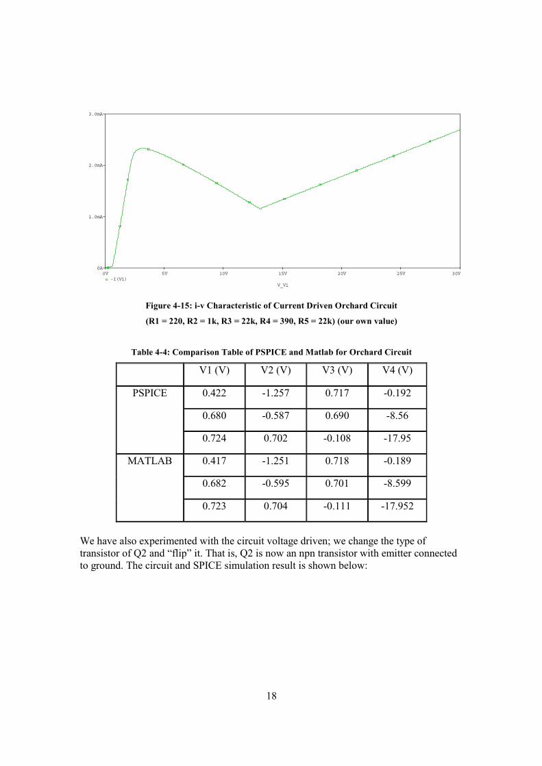
Figure 4-15: i-v Characteristic of Current Driven Orchard Circuit
(R1 = 220, R2 = 1k, R3 = 22k, R4 = 390, R5 = 22k) (our own value)
Table 4-4: Comparison Table of PSPICE and Matlab for Orchard Circuit
V1 (V) V2 (V) V3 (V) V4 (V)
0.422 -1.257 0.717 -0.192
0.680 -0.587 0.690 -8.56
PSPICE
0.724 0.702 -0.108 -17.95
0.417 -1.251 0.718 -0.189
0.682 -0.595 0.701 -8.599
MATLAB
0.723 0.704 -0.111 -17.952
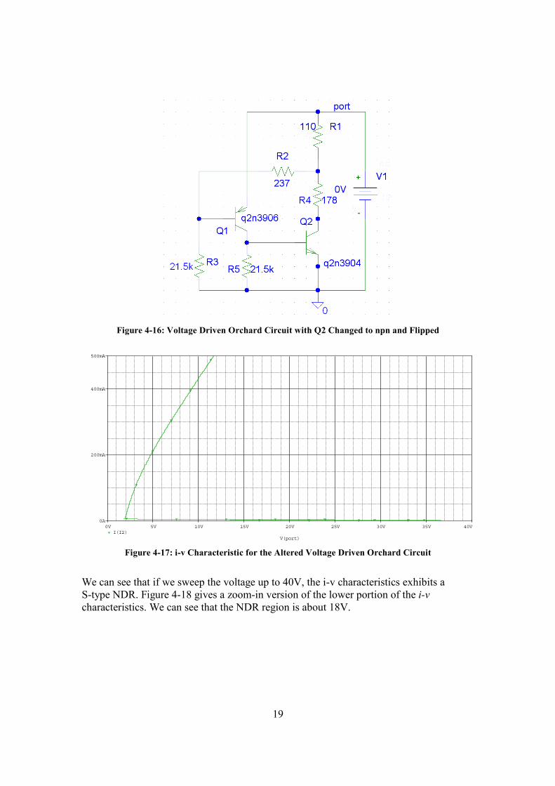
We have also experimented with the circuit voltage driven; we change the type of transistor of Q2 and “flip” it. That is, Q2 is now an npn transistor with emitter connected to ground. The circuit and SPICE simulation result is shown below:
19
Figure 4-16: Voltage Driven Orchard Circuit with Q2 Changed to npn and Flipped
V(port)
0V 5V 10V 15V 20V 25V 30V 35V 40VI(I2)
0A
200mA
400mA
500mA
Figure 4-17: i-v Characteristic for the Altered Voltage Driven Orchard Circuit
We can see that if we sweep the voltage up to 40V, the i-v characteristics exhibits a S-type NDR. Figure 4-18 gives a zoom-in version of the lower portion of the i-v characteristics. We can see that the NDR region is about 18V.
20
V(port)
0V 5V 10V 15V 20V 25V 30V 35V 40VI(I2)
0A
5mA
10mA
15mA
20mA
Figure 4-18: Zoom-in Version of the Lower Portion of Figure 4-17
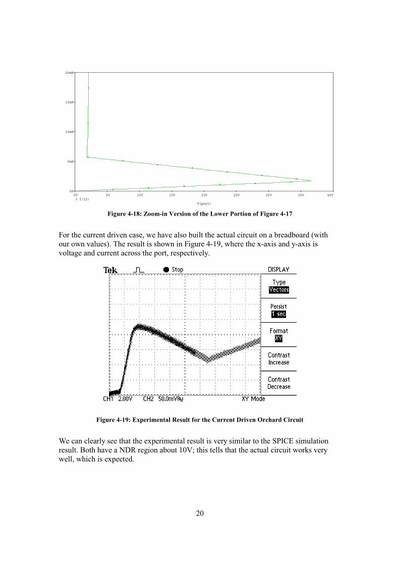
For the current driven case, we have also built the actual circuit on a breadboard (with our own values). The result is shown in Figure 4-19, where the x-axis and y-axis is voltage and current across the port, respectively.
Figure 4-19: Experimental Result for the Current Driven Orchard Circuit
We can clearly see that the experimental result is very similar to the SPICE simulation result. Both have a NDR region about 10V; this tells that the actual circuit works very well, which is expected.
21
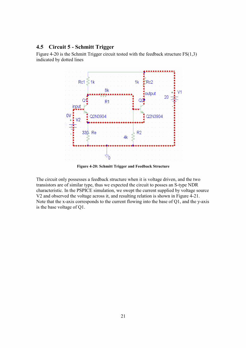
4.5 Circuit 5 - Schmitt Trigger Figure 4-20 is the Schmitt Trigger circuit tested with the feedback structure FS(1,3) indicated by dotted lines
Figure 4-20: Schmitt Trigger and Feedback Structure
The circuit only possesses a feedback structure when it is voltage driven, and the two transistors are of similar type, thus we expected the circuit to posses an S-type NDR characteristic. In the PSPICE simulation, we swept the current supplied by voltage source V2 and observed the voltage across it, and resulting relation is shown in Figure 4-21. Note that the x-axis corresponds to the current flowing into the base of Q1, and the y-axis is the base voltage of Q1.

22
Figure 4-21: i-v Characteristic for the Schmitt Trigger
As we can see, for a voltage value of V2 between 5V and 5.2V there exist three corresponding values of IB1, which translates to an S-type NDR. Similar results were also observed with our MATLAB simulation, where the system is expressed by the equation:
0)( 11 =++ −− CTGTvF . And the determinant c13 corresponding to feedback structure FS(1,3) was evaluated to be -3.668 x 10⁻⁷ < 0, which satisfies the necessary condition for NDR as previously mentioned. Table 4-5 below shows the comparison between the results from PSPICE and Matlab simulation.
Table 4-5: Comparison Table of PSPICE and Matlab for Schmitt Trigger
Solution # V1 (V) V2 (V) V3 (V) V4 (V) 1 -0.476 12.334 -0.739 0.787 2 -0.678 11.358 -0.733 2.62
PSPICE
3 -0.739 0.452 2.65 18.08 1 -0.33 13.112 -0.737 0.605 2 -0.688 10.954 -0.733 3.08
MATLAB
3 -0.734 0.421 2.659 18.093 As we may see, the two sets of resulting junction voltages are in general consistent with each other.
23
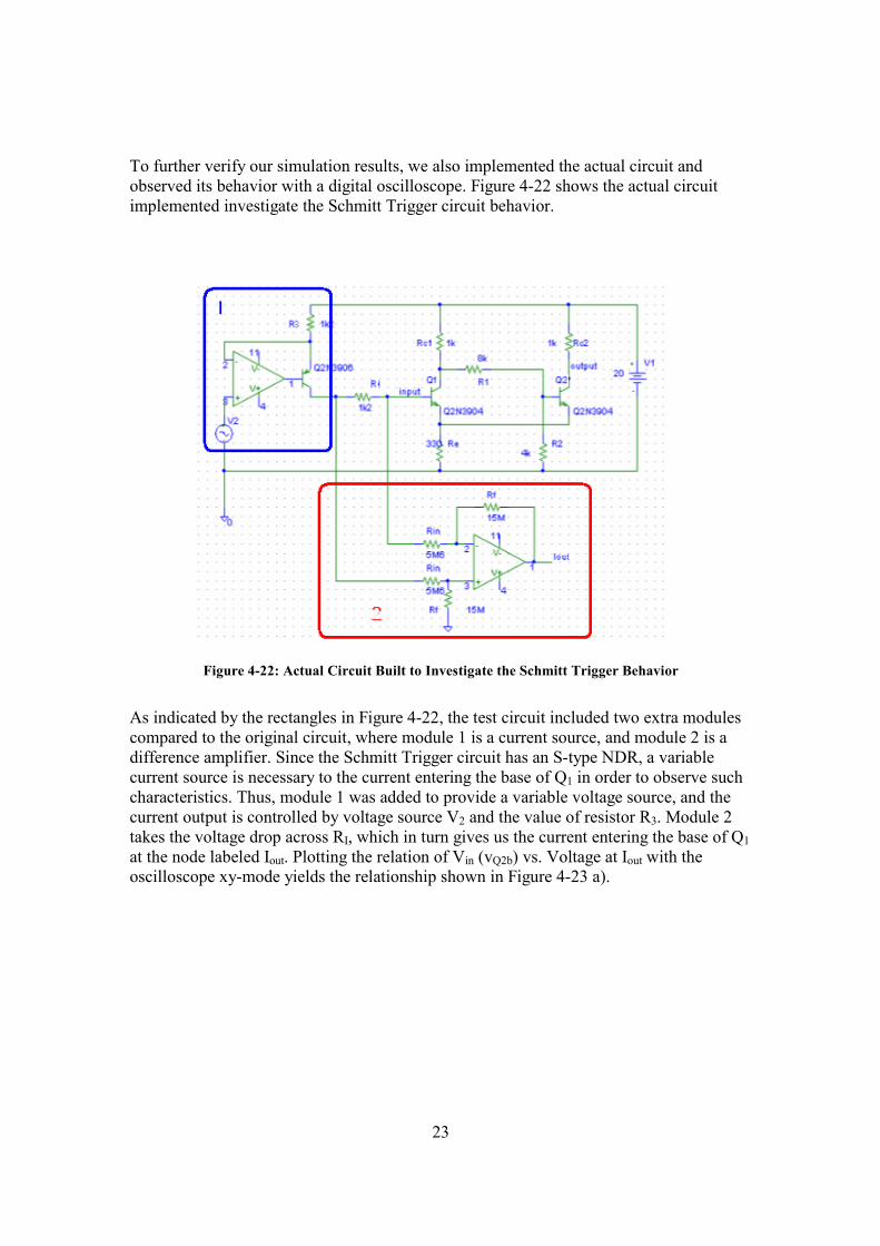
To further verify our simulation results, we also implemented the actual circuit and observed its behavior with a digital oscilloscope. Figure 4-22 shows the actual circuit implemented investigate the Schmitt Trigger circuit behavior.
Figure 4-22: Actual Circuit Built to Investigate the Schmitt Trigger Behavior
As indicated by the rectangles in Figure 4-22, the test circuit included two extra modules compared to the original circuit, where module 1 is a current source, and module 2 is a difference amplifier. Since the Schmitt Trigger circuit has an S-type NDR, a variable current source is necessary to the current entering the base of Q1 in order to observe such characteristics. Thus, module 1 was added to provide a variable voltage source, and the current output is controlled by voltage source V2 and the value of resistor R3. Module 2 takes the voltage drop across RI, which in turn gives us the current entering the base of Q1 at the node labeled Iout. Plotting the relation of Vin (vQ2b) vs. Voltage at Iout with the oscilloscope xy-mode yields the relationship shown in Figure 4-23 a).
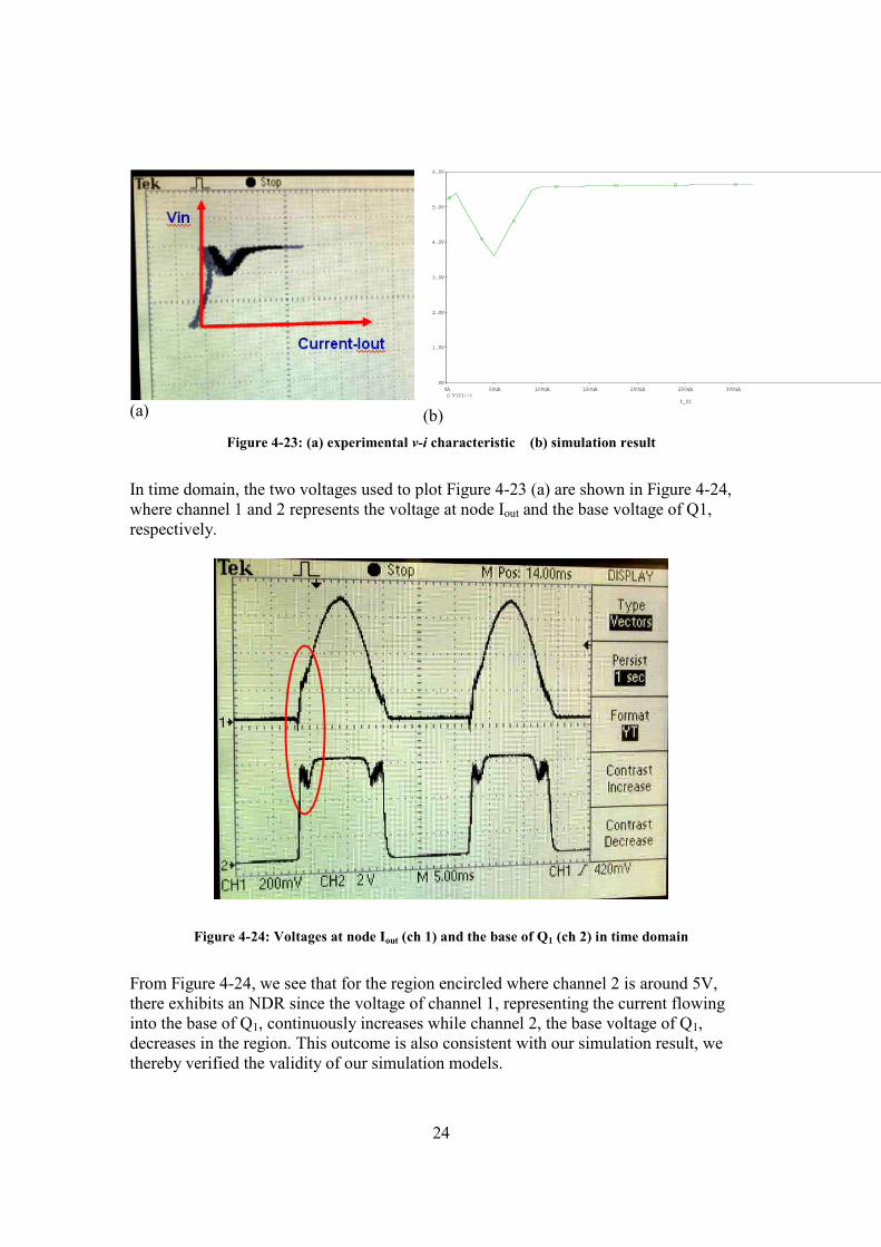
24
Figure 4-23: (a) experimental v-i characteristic (b) simulation result
In time domain, the two voltages used to plot Figure 4-23 (a) are shown in Figure 4-24, where channel 1 and 2 represents the voltage at node Iout and the base voltage of Q1, respectively.
Figure 4-24: Voltages at node Iout (ch 1) and the base of Q1 (ch 2) in time domain
From Figure 4-24, we see that for the region encircled where channel 2 is around 5V, there exhibits an NDR since the voltage of channel 1, representing the current flowing into the base of Q1, continuously increases while channel 2, the base voltage of Q1, decreases in the region. This outcome is also consistent with our simulation result, we thereby verified the validity of our simulation models.
(a) I_I1
0A 50uA 100uA 150uA 200uA 250uA 300uAV(I1:-)
0V
1.0V
2.0V
3.0V
4.0V
5.0V
6.0V
(b)

25
5 Discussion In the process of simulating circuits with different approaches, we have observed some minor discrepancies between results obtain with different tools. In general, more differences were more significant between the simulation results for v2’s and v4’s, which correspond to the collector-to-base voltages of Q1 and Q2 of each circuit. This can be explained qualitatively by considering the nature of a properly biased transistor, which has its terminal currents depend mostly on the emitter-to-base voltage (v1 or v3), and rather insensitive to changes in the collector-to-base voltage. In other words, significant changes in collector-to-base voltages will result in negligible effect on the overall behavior of the transistor, providing the transistor remains in the same operating region. Therefore, minor differences between the models used in PSPICE and MATLAB could cause observable discrepancies in the simulation results for v2’s and v4’s. A few other points worth mentioning are related to the Schmitt trigger circuit. Figure 5-1 shows a screen capture of the output voltage vs. input voltage of the Schmitt trigger.
Figure 5-1:Vout v.s. Vin Relation of Schmitt Trigger.
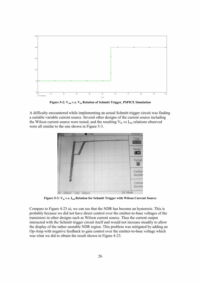
This relation was not observed with PSPICE, in which only the forward step is shown in Figure 5-2. This is due to the fact that PSPICE is incapable of solving and displaying multiple solutions of the circuit at the same time, thus the resulting plot is a single step instead of the hysteresis observed in a real circuit.
26
V_V2
0V 1V 2V 3V 4V 5V 6V 7V 8V 9V 10VV(output)
0V
5V
10V
15V
20V
25V
Figure 5-2: Vout v.s. Vin Relation of Schmitt Trigger, PSPICE Simulation
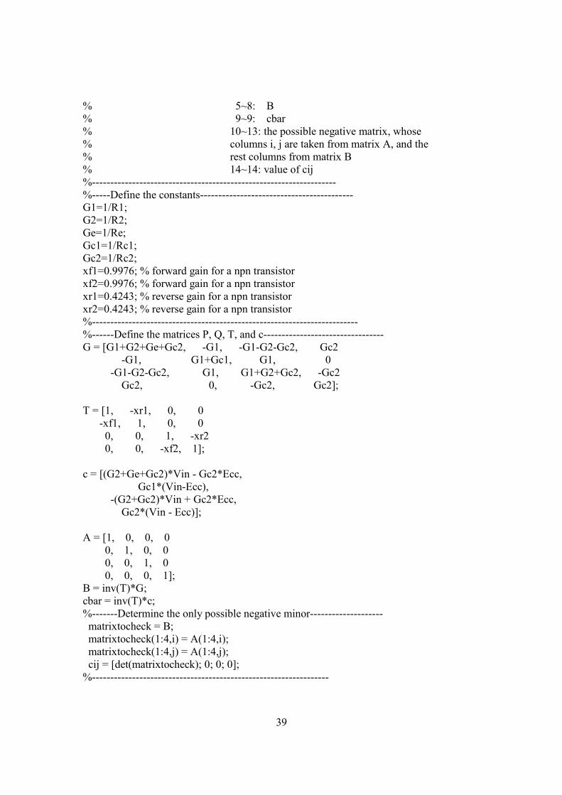
A difficulty encountered while implementing an actual Schmitt trigger circuit was finding a suitable variable current source. Several other designs of the current source including the Wilson current source were tested, and the resulting Vin vs Iout relations observed were all similar to the one shown in Figure 5-3.
Figure 5-3: Vin v.s. Iout Relation for Schmitt Trigger with Wilson Current Source
Compare to Figure 4-23 a), we can see that the NDR has become an hysteresis. This is probably because we did not have direct control over the emitter-to-base voltages of the transistors in other designs such as Wilson current source. Thus the current output interacted with the Schmitt trigger circuit itself and would not increase steadily to allow the display of the rather unstable NDR region. This problem was mitigated by adding an Op-Amp with negative feedback to gain control over the emitter-to-base voltage which was what we did to obtain the result shown in Figure 4-23.

27
6 Conclusion In this project we have investigated the necessary conditions for a two-transistor circuit to possess multiple operating points and exhibit NDR behavior and used them as a start point to help us identify if a circuit can potentially exhibit NDR behavior. In addition, theory of dc operating points of transistor networks from various papers was used as a reference along the way. We have successfully verified and illustrated that the five circuits we have investigated can all exhibit NDR behaviour when current and/or voltage driven. Some circuits can potentially possess nice and long NDR region; while others, at NDR occurrence, exhibit only very narrow NDR region. This phenomenon can be explained by the natural purpose of the circuit. For example, the Orchard circuit exhibits long and smooth NDR region since it is designed to be a negative resistance device; while Schmitt trigger’s NDR region is very narrow since it is designed to be a trigger (i.e., operating point tend to switch toward the two ends and very unlikely stay at the middle operating point).

28
7 References [1] Lj. Trajkovic and A. N. Wilson, Jr., “Biasing of Two Transistor Circuits Exhibiting Negative Differential Resistance,” Electrical Engineering Department, UCLA, CA, 1987. [2] Lj. Trajkovic and A. N. Wilson, Jr., “Behavior of Nonlinear Transistor One-Ports: Things are not Always as Simple as Might be Expected,” Electrical Engineering Department, UCLA, CA, 1988. [3] Lj. Trajkovi´c and A. N. Willson, Jr., “Theory of dc operating points of transistor networks,” Intern. Journ. Electronics and Comm., vol. 46, no. 6, pp. 228–241, July 1992. [4] R. O. Nielsen and A. N. Willson, Jr., “Existence of hybrid matrices for active n-ports encountered in the analysis of transistor networks,” Int. J. Circuit Theory and Appl., vol. 7, pp. 65–76, Jan. 1979.

29
8 Appendix
8.1 Circuit 1 – Flip Flop % file: flipflopconstants.m function [FuncProp] = flipflopconstants(Rb1,Rb2,Rc1,Rc2,Ebb1,Ebb2,i,j) %----------------------------------------------------- % Description: % This function returns the matrix properties of the nonlinear equation % A*F(v) + B*v + cbar = 0 % i.e., the matrix A, B, as well as matrix cbar, which contains the % biasing information, depending on the circuit is voltage or current driven. % Since in this circuit G matrix exists => % -i = G*v + c and i = T*F(v) => -T*F(v) = G*v + c % => T*F(v) + G*v + c = 0 => F(v) + inv(T)*G*v + inv(T)*c = 0 % i.e., in this circuit, A = I (identity matrix), B = inv(T)*G, cbar = inv(T)*c % Input: % Rb1, Rb2, Rc1, Rc2: values of resistors % Ebb1,Ebb2: biasing voltage value (i.e., voltage driven) % i,j: feedback structure for calculating the only possible negative coefficient % Output: % FuncProp: a stack which consists of A, B, c, and cij % columns 1~4: A % 5~8: B % 9~9: cbar % 10~13: the possible negative coefficient, whose % columns i, j are taken from matrix A, and % the rest columns from matrix B % 14~14: value of cij %----------------------------------------------------------------------- %-----Define the constants------------------------------------------ Gb1=1/Rb1; Gb2=1/Rb2; Gc1=1/Rc2; Gc2=1/Rc2; xf1=0.9976; % forward gain for a npn transistor xf2=0.9976; % forward gain for a npn transistor xr1=0.4243; % reverse gain for a npn transistor xr2=0.4243; % reverse gain for a npn transistor %------------------------------------------------------------------------- %------Define the matrices P, Q, T, and c--------------------------------- G = [Gb1+Gb2+Gc1, -(Gc1+Gb2), -(Gb1+Gb2), Gb1 -(Gc1+Gb2), Gc1+Gb2, Gb2, 0 -(Gb1+Gb2), Gb2, Gb1+Gb2+Gc2, -(Gc2+Gb1) Gb1, 0, -(Gc2+Gb1), Gc2+Gb1];

30
T = [1, -xr1, 0, 0 -xf1, 1, 0, 0 0, 0, 1, -xr2 0, 0, -xf2, 1]; A = [1, 0, 0, 0 0, 1, 0, 0 0, 0, 1, 0 0, 0, 0, 1]; B = inv(T)*G; c = [Gc1*Ebb1, -Gc1*Ebb1, Gc2*Ebb2, -Gc2*Ebb2]; cbar = inv(T)*c; %-------Determine the only possible negative minor-------------------- matrixtocheck = B; matrixtocheck(1:4,i) = A(1:4,i); matrixtocheck(1:4,j) = A(1:4,j); cij = [det(matrixtocheck); 0; 0; 0]; %----------------------------------------------------------------- FuncProp = [A, B, cbar, matrixtocheck, cij]; % file: flipflop.m function y = flipflop(v) %------------------------------------------------------------------- % Description: % This function defines the set of nonlinear equations to solve. % y = A*F(v) + B*v + cbar = 0 % where F(v) = ( f1(v1), f2(v2), f3(v3), f4(v4) )t, % and fi(vi) = mi(exp(ni*vi) - 1), mi, ni > 0 for pnp and < 0 for npn % ni = q/kT and mi = Ie or Ic (emitter or collector saturation current) % which is calculated to be around 38.61 %------------------------------------------------------------------- FuncInfo = flipflopconstants(30000,40000,5000,2000,12,8,1,3); % call the "flipflopconstants" function and input resistor values, Vin, Ecc, and feedback structure A = FuncInfo(1:4,1:4); B = FuncInfo(1:4,5:8); c = FuncInfo(1:4,9); % extract matrix A, B, and cbar Ie04 = 6.734E-15; % Isat for emitter, for a npn transistor, obtained from PSPICE Ic04 = 15.833E-15; % Isat for collector, for a npn transistor, obtained from PSPICE

31
y = A*[-Ie04*(exp(-38.61*v(1))-1);-Ic04*(exp(-38.61*v(2))-1);-Ie04*(exp(-38.61*v(3))-1);-Ic04*(exp(-38.61*v(4))-1)] + B*[v(1);v(2);v(3);v(4)] + c; % file: flipflopmain.m %------------------------------------------------------------------ % Main program for the Flip-Flop circuit % Description: % In this main program, first we have to choose an initial point for each % function f(v) that is "close" enough to the actual solution, obtained % from PSPICE simulation result. Then the "fsolve" command is used to % solve the set of nonlinear equations, and the answer is stored in a % stach "Vschmitt". The properties of this nonlinear equation are also % stored in a stack "FuncInfo". %--------------------------------------------------------------------- FuncInfo = flipflopconstants(30000,40000,5000,2000,12,8,1,3); init = [-0.7 -0.02 -0.6 6]; % choose the initial point for each fi(vi) Vflopflop = fsolve(@flipflop,init,optimset('TolX',0.0001,'Display','iter'));
8.2 Circuit 2 % file: ckt2Edrivenconst.m function [FuncProp] = ckt2Edrivenconst(R1,R2,R3,Vs,i,j) %----------------------------------------------------- % Description: % This function returns the matrix properties of the nonlinear equation % A*F(v) + B*v + c = 0 % i.e., the matrix A, B, as well as matrix c, which contains the % biasing information, depending the circuit is voltage or current driven % P*v + Q*i + c = 0 and i = T*F(v) => Q*T*F(v) + P*v + c = 0 % i.e., in this circuit, A = Q*T, B = P % Input: % R1, R2, R3: values of resistors % Vs: biasing voltage value (i.e., voltage driven) % i,j: feedback structure for calculating the only possible nagative % coefficient cij % Output: % FuncProp: a stack which consists of A, B, c, and cij % columns 1~4: A % 5~8: B % 9~9: c % 10~13: matrix whose columns i,j are taken from A % and the rest from B, without changing the order % 14~14: value of cij %-----Define the constants------------------------------------------------- Ie04 = 6.734E-15; % Isat for emitter, for a npn transistor, obtained from PSPICE

32
Ic04 = 15.833E-15; % Isat for collector, for a npn transistor, obtained from PSPICE Ie06 = 1.41E-15; % Isat for emitter, for a pnp transistor, obtained from PSPICE Ic06 = 1.684E-15; % Isat for collector, for a pnp transistor, obtained from PSPICE Rt=R1+R2+R3; xf1=0.9976; % forward gain for a npn transistor xr1=0.4243; % reverse gain for a npn transistor xf2=0.9944; % forward gain for a pnp transistor xr2=0.8326; % reverse gain for a pnp transistor %------------------------------------------------------------------------- %------Define the matrices P, Q, T, and c--------------------------------- P = [0, 0, 0, 0 0, 1, 1, 0 -1, 1, 0, 1 1, 0, 0, 0]; Q = [ 0, 1, -1, -1 ((R2+R3)*R1)/Rt, ((R2+R3)*R1)/Rt, 0, -(R1*R3)/Rt -(1-(R2+R3)/Rt)*R3, -(1-(R2+R3)/Rt)*R3, 0, (1-(R3/Rt))*R3 ((R2+R3)*R1)/Rt, ((R2+R3)*R1)/Rt, 0, -(R1*R3)/Rt]; T = [ 1, -xr1, 0, 0 -xf1, 1, 0, 0 0, 0, 1, -xr2 0, 0, -xf2, 1]; c = [ 0 -(R1/Rt)*Vs -(R3/Rt)*Vs (1-(R1/Rt))*Vs]; A = Q*T; B = P; %-------Determine the only possible negative minor-------------------- matrixtocheck = B; matrixtocheck(1:4,i) = A(1:4,i); matrixtocheck(1:4,j) = A(1:4,j); cij = [det(matrixtocheck);0;0;0]; %----------------------------------------------------------------- FuncProp = [A, B, c, matrixtocheck, cij]; % file: ckt2.m function y = ckt2(v) %------------------------------------------------------------------- % Description: % This function defines the set of nonlinear equations to solve. % y = A*F(v) + B*v + c = 0

33
% where F(v) = ( f1(v1), f2(v2), f3(v3), f4(v4) )t, % and fi(vi) = mi(exp(ni*vi) - 1), mi, ni > 0 for pnp and < 0 for npn % ni = q/kT and mi = Ie or Ic (emitter or collector saturation current) % which is calculated to be about 38.61 %------------------------------------------------------------------- FuncInfo = ckt2Edrivenconst(10,3000,10,1.1,1,3); %FuncInfo = ckt2Idrivenconst(11000,3000,2000,10e-3,1,4); % call the "ckt2Edrivenconst" or "ckt2Idrivenconst" function, depending on % whether the circuit is voltage or current driven, and input resistor values, % biasing information (i.e, Is or Vs) and feedback structure A = FuncInfo(1:4,1:4); B = FuncInfo(1:4,5:8); c = FuncInfo(1:4,9); % extract matrix A, B, and c Ie04 = 6.734E-15; % Isat for emitter, for a npn transistor, obtained from PSPICE Ic04 = 15.833E-15; % Isat for collector, for a npn transistor, obtained from PSPICE Ie06 = 1.41E-15; % Isat for emitter, for a pnp transistor, obtained from PSPICE Ic06 = 1.684E-15; % Isat for collector, for a pnp transistor, obtained from PSPICE % saturation currents for Q2N3904 (npn) transistor y = A*[-Ie04*(exp(-38.61*v(1))-1);-Ic04*(exp(-38.61*v(2))-1);Ie06*(exp(38.61*v(3))-1);Ic06*(exp(38.61*v(4))-1)] + B*[v(1);v(2);v(3);v(4)] + c; % file: ckt2main.m %------------------------------------------------------------------------ % Main program for circuit #2 % Description: % In this main program, first we have to choose an initial point for each % function f(v) that is "close" enough to the actual solution, obtained % from PSPICE simulation result. Then the "fsolve" command is used to % solve the set of nonlinear equations, and the answer is stored in a % stack "Vckt2". The properties of this nonlinear equation, obtained from % "ckt2Edrivenconst" or "ckt2Idrivenconst" function, are also stored in a stack "FuncInfo". %-------------------------------------------------------------------------- FuncInfo = ckt2Edrivenconst(15000,5000,10,1.1,1,3); %FuncInfo = ckt2Idrivenconst(11000,3000,2000,10e-3,1,4); init = [0 0 0 0]; % choose the initial point for each v Vckt2=fsolve(@ckt2,init,optimset('TolX',0.001,'Display','iter'));
8.3 Circuit 3 % file: constants.m function [FuncProp] = constants(R1,R2,R3,Is,i,j) %----------------------------------------------------- % Description:

34
% This function returns the matrix properties of the nonlinear equation % A*F(v) + B*v + cbar = 0 % i.e., the matrix A, B, as well as matrix cbar, which contains the % biasing information, depending the circuit is voltage or current driven % (feedback structure exists only when the circuit is current % driven; therefore, the matrices here are only for the current driven case % P*v + Q*i = c and i = T*F(v) => Q*T*F(v) + P*v - c = 0 % i.e., in this circuit, A = Q*T, B = P % Input: % R1, R2, R3: values of resistors % Is: biasing current value (i.e., current driven) % i,j: feedback structure for calculating the only possible % nagative coefficient % Output: % FuncProp: a stack which consists of A, B, c, and cij % columns 1~4: A % 5~8: B % 9~9: c % 10~13: matrix whose columns i,j are taken from A % and the rest from B, without changing the order % 14~14: value of cij %-----Define the constants------------------------------------------------- G1=1/R1; G2=1/R2; G3=1/R3; xf1=0.9976; % forward gain for a npn transistor xr1=0.4243; % reverse gain for a npn transistor xf2=0.9976; % forward gain for a npn transistor xr2=0.4243; % reverse gain for a npn transistor %------------------------------------------------------------------------- %------Define the matrices P, Q, T, and c--------------------------------- P = [-G2, 0, 0, 0 1, -1, -1, 0 0, 0, 0, G3 G2, G1, 0, G1]; Q = [-1, 0, -1, 0 0, 0, 0, 0 0, -1, 1, 1 1, 1, 0, 0]; T = [1, -xr1, 0, 0 -xf1, 1, 0, 0 0, 0, 1, -xr2 0, 0, -xf2, 1];

35
c = [Is 0 0 0]; A = Q*T; B = P; %------------------------------------------------------------------------------- %-------Determine the only possible negative minor-------------------- matrixtocheck = B; matrixtocheck(1:4,i) = A(1:4,i); matrixtocheck(1:4,j) = A(1:4,j); cij = [det(matrixtocheck); 0; 0; 0]; %------------------------------------------------------------------------------- FuncProp = [A, B, c, matrixtocheck, cij]; % file: circuit5.m function y = circuit5(v) %------------------------------------------------------------------- % Description: % This function defines the set of nonlinear equations to solve. % y = A*F(v) + B*v + c = 0 % where F(v) = ( f1(v1), f2(v2), f3(v3), f4(v4) )t, % and fi(vi) = mi(exp(ni*vi) - 1), mi, ni > 0 for pnp and < 0 for npn % ni = q/kT and mi = Ie or Ic (emitter or collector saturation current) % which is calculated to be about 38.61 %------------------------------------------------------------------- FuncInfo = constants(2200,470,10000,9.2E-3,1,3); % call the "constants" function and input resistor values, I, and feedback structure A = FuncInfo(1:4,1:4); B = FuncInfo(1:4,5:8); c = FuncInfo(1:4,9); % extract matrix A, B, and c Ie04 = 6.734E-15; % Isat for emitter, for a npn transistor, obtained from PSPICE Ic04 = 15.833E-15; % Isat for collector, for a npn transistor, obtained from PSPICE y = A*[-Ie04*(exp(-38.61*v(1))-1);-Ic04*(exp(-38.61*v(2))-1);-Ie04*(exp(-38.61*v(3))-1);-Ic04*(exp(-38.61*v(4))-1)] + B*[v(1);v(2);v(3);v(4)] - c; % file: circuit5main.m %------------------------------------------------------------------ % Main program for circuit #5 % Description: % In this main program, first we have to choose an initial point for each % function f(v) that is "close" enough to the actual solution, obtained % from PSPICE simulation result. Then the "fsolve" command is used to

36
% solve the set of nonlinear equations, and the answer is stored in a % stack "Vckt5". The properties of this nonlinear equation, obtained from % "constants" function, are also stored in a stack "FuncInfo". %--------------------------------------------------------------------- FuncInfo = constants(2200, 470, 10000, 9.2E-3, 1, 3); init = [0 0 0 0]; % choose the initial point for each v Vckt5=fsolve(@circuit5,init,optimset('TolX',0.001,'Display','iter'));
8.4 Circuit 4 – Orchard % file: orchardconst.m function [FuncProp] = orchardconst(R1,R2,R3,R4,R5,Is,i,j) %----------------------------------------------------- % Description: % This function returns the matrix properties of the nonlinear equation % A*F(v) + B*v + c = 0 % i.e., the matrix A, B, as well as matrix c, which contains the % biasing information, depending the circuit is voltage or current driven % P*v + Q*i + c = 0 and i = T*F(v) => Q*T*F(v) + P*v + c = 0 % i.e., in this circuit, A = Q*T, B = P % Input: % R1, R2, R3, R4, R5: values of resistors % Is: biasing current value (i.e., current driven) % i,j: feedback structure for calculating the only possible nagative % coefficient % Output: % FuncProp: a stack which consists of A, B, c, and cij % columns 1~4: A % 5~8: B % 9~9: c % 10~13: matrix whose columns i,j are taken from A % and the rest from B, without changing the order % 14~14: value of cij %-----Define the constants------------------------------------------------- G1=1/R1; G2=1/R2; G3=1/R3; G4=1/R4; G5=1/R5; xf1=0.9944; % forward gain for a pnp transistor xf2=0.9944; % forward gain for a pnp transistor xr1=0.8326; % reverse gain for a pnp transistor xr2=0.8326; % reverse gain for a pnp transistor %------Define the matrices P, Q, T, and c--------------------------------- Po = [0, R5, 0, R3+R5 0, 0, 0, 1

37
R3, R1+R2, 0, R1+R2 0, R2+R3, R3, R2]; Qo = [ 0, 0, 0, R3*R5 0, -R5, R5, R5 R3*(R1+R2), R3*(R1+R2), -R1*R3, 0 R2*R3, R2*R3, R3*R4, 0]; To = [ 1, -xr1, 0, 0 -xf1, 1, 0, 0 0, 0, 1, -xr2 0, 0, -xf2, 1]; co = [Is*R3*R5 0 0 0]; Ao = Qo*To; Bo = Po; %-------Determine the only possible negative minor-------------------- matrixtochecko = Bo; matrixtochecko(1:4,i) = Ao(1:4,i); matrixtochecko(1:4,j) = Ao(1:4,j); cijo = [det(matrixtochecko); 0; 0; 0]; %----------------------------------------------------------------- FuncProp = [Ao, Bo, co, matrixtochecko, cijo]; % file: Orchard.m function yo = orchard(v) %------------------------------------------------------------------- % Description: % This function defines the set of nonlinear equations to solve. % y = A*F(v) + B*v + c = 0 % where F(v) = ( f1(v1), f2(v2), f3(v3), f4(v4) )t, % and fi(vi) = mi(exp(ni*vi) - 1), mi, ni > 0 for pnp and < 0 for npn % ni = q/kT and mi = Ie or Ic (emitter or collector saturation current) % which is calculated to be about 38.61 %------------------------------------------------------------------- FuncInfo = orchardconst(110,237,21500,178,21500,-1.6E-3,1,3);% from the original circuit values A = FuncInfo(1:4,1:4); B = FuncInfo(1:4,5:8); c = FuncInfo(1:4,9); % extract matrices A, B, c

38
Ie06 = 1.41E-15; % Isat for emitter, for a pnp transistor, obtained from PSPICE Ic06 = 1.684E-15; % Isat for collector, for a pnp transistor, obtained from PSPICE y = A*[Ie06*(exp(38.61*v(1))-1);Ic06*(exp(38.61*v(2))-1);Ie06*(exp(38.61*v(3))-1);Ic06*(exp(38.61*v(4))-1)] + B*[v(1);v(2);v(3);v(4)] + c; % file: Orchardmain.m %--------------------------------------------------------------------------------------------- % Description: % In this main program, first we have to choose an initial point for each % function f(v) that is "close" enough to the actual solution, obtained % from PSPICE simulation result. Then the "fsolve" command is used to % solve the set of nonlinear equations, and the answer is stored in a % stack "Vorchard". The properties of this nonlinear equation, obtained from % "orchardconst" function, are also stored in a stack "FuncInfo". %--------------------------------------------------------------------------------------------- FuncInfo = orchardconst(110,237,21500,178,21500,-1.6E-3,1,3); orchardinit = [.45 -1 -.6 -8]; % choose the initial point for each v Vorchard = fsolve(@orchard,orchardinit,optimset('TolX',0.001,'Display','iter'));
8.5 Circuit 5 – Schmitt Trigger % file: schmittconstants.m function [FuncProp] = schmittconstants(R1,R2,Rc1,Rc2,Re,Vin,Ecc,i,j) %----------------------------------------------------- % Description: % This function returns the matrix properties of the nonlinear equation % A*F(v) + B*v + cbar = 0 % i.e., the matrix A, B, as well as matrix cbar, which contains the % biasing information, depending on the circuit is voltage or current % driven (note: feedback structure exists only when the circuit is voltage % driven; therefore, the matrices here are only for the voltage driven % case) % Since in this circuit G matrix exists => % -i = G*v + c and i = T*F(v) => -T*F(v) = G*v + c % => T*F(v) + G*v + c = 0 => F(v) + inv(T)*G*v + inv(T)*c = 0 % i.e., in this circuit, A = I (identity matrix), B = inv(T)*G, cbar = inv(T)*c % Input: % R1, R2, Rc1, Rc2, Re: values of resistors % Vin: biasing voltage value (i.e., voltage driven) % Ecc: power supply voltage % i,j: feedback structure for calculating the only possible nagative % coefficient cij % Output: % FuncProp: a stack which consists of A, B, c, and cij % columns 1~4: A
39
% 5~8: B % 9~9: cbar % 10~13: the possible negative matrix, whose % columns i, j are taken from matrix A, and the % rest columns from matrix B % 14~14: value of cij %------------------------------------------------------------------- %-----Define the constants------------------------------------------ G1=1/R1; G2=1/R2; Ge=1/Re; Gc1=1/Rc1; Gc2=1/Rc2; xf1=0.9976; % forward gain for a npn transistor xf2=0.9976; % forward gain for a npn transistor xr1=0.4243; % reverse gain for a npn transistor xr2=0.4243; % reverse gain for a npn transistor %------------------------------------------------------------------------- %------Define the matrices P, Q, T, and c--------------------------------- G = [G1+G2+Ge+Gc2, -G1, -G1-G2-Gc2, Gc2 -G1, G1+Gc1, G1, 0 -G1-G2-Gc2, G1, G1+G2+Gc2, -Gc2 Gc2, 0, -Gc2, Gc2]; T = [1, -xr1, 0, 0 -xf1, 1, 0, 0 0, 0, 1, -xr2 0, 0, -xf2, 1]; c = [(G2+Ge+Gc2)*Vin - Gc2*Ecc, Gc1*(Vin-Ecc), -(G2+Gc2)*Vin + Gc2*Ecc, Gc2*(Vin - Ecc)]; A = [1, 0, 0, 0 0, 1, 0, 0 0, 0, 1, 0 0, 0, 0, 1]; B = inv(T)*G; cbar = inv(T)*c; %-------Determine the only possible negative minor-------------------- matrixtocheck = B; matrixtocheck(1:4,i) = A(1:4,i); matrixtocheck(1:4,j) = A(1:4,j); cij = [det(matrixtocheck); 0; 0; 0]; %-----------------------------------------------------------------

40
FuncProp = [A, B, cbar, matrixtocheck, cij]; % file: schmitt.m function y = schmitt(v) %------------------------------------------------------------------- % Description: % This function defines the set of nonlinear equations to solve. % y = A*F(v) + B*v + cbar = 0 % where F(v) = ( f1(v1), f2(v2), f3(v3), f4(v4) )t, % and fi(vi) = mi(exp(ni*vi) - 1), mi, ni > 0 for pnp and < 0 for npn % ni = q/kT and mi = Ie or Ic (emitter or collector saturation current) % which is calculated to be around 38.61 %------------------------------------------------------------------- FuncInfo = schmittconstants(8000,4000,1000,1000,330,5.30,20,1,3); % call the "schmittconstants" function and input resistor values, Vin, Ecc, and feedback structure A = FuncInfo(1:4,1:4); B = FuncInfo(1:4,5:8); cbar = FuncInfo(1:4,9); % extract matrix A, B, and cbar Ie04 = 6.734E-15; % Isat for emitter, for a npn transistor, obtained from PSPICE Ic04 = 15.833E-15; % Isat for collector, for a npn transistor, obtained from PSPICE y = A*[-Ie*(exp(-38.61*v(1))-1);-Ic*(exp(-38.61*v(2))-1);-Ie*(exp(-38.61*v(3))-1);-Ic*(exp(-38.61*v(4))-1)] + B*[v(1);v(2);v(3);v(4)] + cbar; % file: schmittmain.m %------------------------------------------------------------------ % Main program for the Schmitt Trigger circuit % Description: % In this main program, first we have to choose an initial point for each % function f(v) that is "close" enough to the actual solution, obtained % from PSPICE simulation result. Then the "fsolve" command is used to % solve the set of nonlinear equations, and the answer is stored in a % stack "Vschmitt". The properties of this nonlinear equation, obtained from % "schmittconstants" function, are also stored in a stack "FuncInfo". %--------------------------------------------------------------------- FuncInfo = schmittconstants(11000,8000,1000,1000,330,5.3,10,1,3); init = [-1 0 0 0]; % choose the initial point for each fi(vi) Vschmitt = fsolve(@schmitt,init,optimset('TolX',0.0001,'Display','iter'));