Embed Size (px)
Citation preview

Solar cell fabrication technology
Vítězslav Benda, CTU Prague, Faculty of Electrical Engineering

Market share by solar cell technologies
At present, nearly 90% of solar cell production is made from crystalline silicon

Preparing semicondutor silicon
arc furnace
silicon grinding Cl2 - drying
electrolysis
HCl - production
H2 - purification
condensation polysilicon processing
polysilicon deposition with doping
high purity distillation
distillation
condensation
fluid-bed reactor, SiHCl3 - production
NaCl
NaOH
SiCl4
CD
C SiO2

Polycrystalline silicon fabrication
SiHCl3 + H2 → Si + 3HCl

Monocrystalline silicon fabrication (Czochralski method)
- diameter up to 450 mm
- weight up to 300 kg

Single-crystal fabrication
polycrystalline silicon processing
FZ-pulling CZ-pulling slim-rod pulling
single crystal rod shaping
Wafer fabrication
crystalline silicon shaped rod
sawing
lapping
etch rounding
cleaning
polishing
microelectronics grade quality wafer
sawing
etching and cleaning
solar cell grade quality wafer

Multicrystalline rod fabrication

Wafer fabrication
isotropic etching (HF + HNO3 + CH3COOH)
texturing by anisotropic etching
~40% of material is lost during crystalline rod cutting (sawing)

Ribbon silicon
EFG (Edge-defined Film-fed Growth)
method
(~ 300 µm thick polycrystalline silicon sheets)
The ribbons are prepared in a form of a hollow octagonal tube (5 m in length) with eight 100 – 125 mm wide faces.

Diffusion technology
PN junction is usually realised by phosphorous diffusion into P-type basic material
N x t N erfcx
Dt( , ) 0
N x tQ
Dt
x
Dt, exp
2
4
ND(xj;tdiff) = NA
kT
WDTD exp)( 0


The structure of a high efficient solar cell (PERL) made from monkrystalline silicon (efficiency 24%)
very expensive technology
FZ starting material
microelectronics quality wafers
photolihography
anisotropic etching
diffusion
AR coating
photolithography
contact deposition

To decrease the fabrication cost….
•CZ quality material•Wire-cut wafers•Chemical surface processing (texturing)
•To avoid expensive fabrication techniques like photolithography and vacuum deposition techniques
- etching monocrystalline (1,0,0) Si in KOH
- acid etching in the case of other crystallographic orientation of Si

Standard mass production (c-Si cells)
• chemical surface texturing
• SiN(H) antireflection surface coating and passivation
• contact grid realised by the screen print technique

Fabrication of c-Si solar cells
c-Si wafer
- etching of damaged layer- texturing- N-type (P) diffusion
- Si3N4 ARC- Ag/Al print screen BS- Ag print screen FS
- firing of contact pastes
- edge grinding
- measuring and sorting

Crystalline Si solar cells
mono-crystalline multi-crystalline
17%
16%
(area up to 400 cm2)
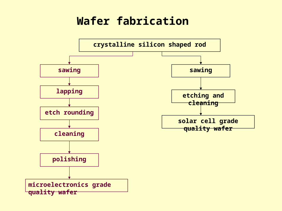
rubber sealing
hardened glass
EVA
solar cellsback covering foil (tedlar)Al frame
solar cell
PV module
PV module technology
Module lifetime
> 20 years

- between two glass sheets
- sealing compound application
- hind side from non-transparent material
- laminate foil application
Alternative module constructions

Thin film solar cell technology
A) Vacuum deposition
Filament evaporation
Electron-beam evaporation
Flash evaporation
Sputtering

TCO for „light trapping effect“
ZnO sputtered and etched in HCl
ZnO prepared by CVD (Chemical Vapour Deposition)

B) CVD (Chemical vapour deposition ) technique
CVD technology is the formation of a stable compound on a heated substrate by the thermal reaction or decomposition of gaseous compounds
• Reaction chamber• Gas control section• Timing and sequence control• Heat source for substrates• Effective handling.

Atmosphere CVD
Low pressure CVD (LPCVD)
LPCVD is used for deposition of silicon nitride 3SiH4 + 3NH3 → Si3N4 + 12H2
deposition polysilicon layers SiH4 → Si + 2H2.

Plasma enhanced CVD (PECVD)
RF electrode and substrate create the capacitor structure. In this space the plasma and incorporated deposition of material on substrate takes place
The deposition rate is higher than in the case of LPCVD, but layer quality is lower

Hot wire chemical vapour deposition (HWCVD)
This technique relies on the catalytic decomposition of SiH4 by metal.
A filament is a basic component in this system.
The gas in presence of a heated filament (the filament material is W or Ta) is decomposed in radicals that diffuse to and are deposited on the substrate

The deposited layer structure depends on the gas composition and substrate temperature
dilution ratio rH = ([H2] + [SiH4])/[SiH4]. rH < 30, amorphous silicon growth
rH > 45, crystalline layers are formed
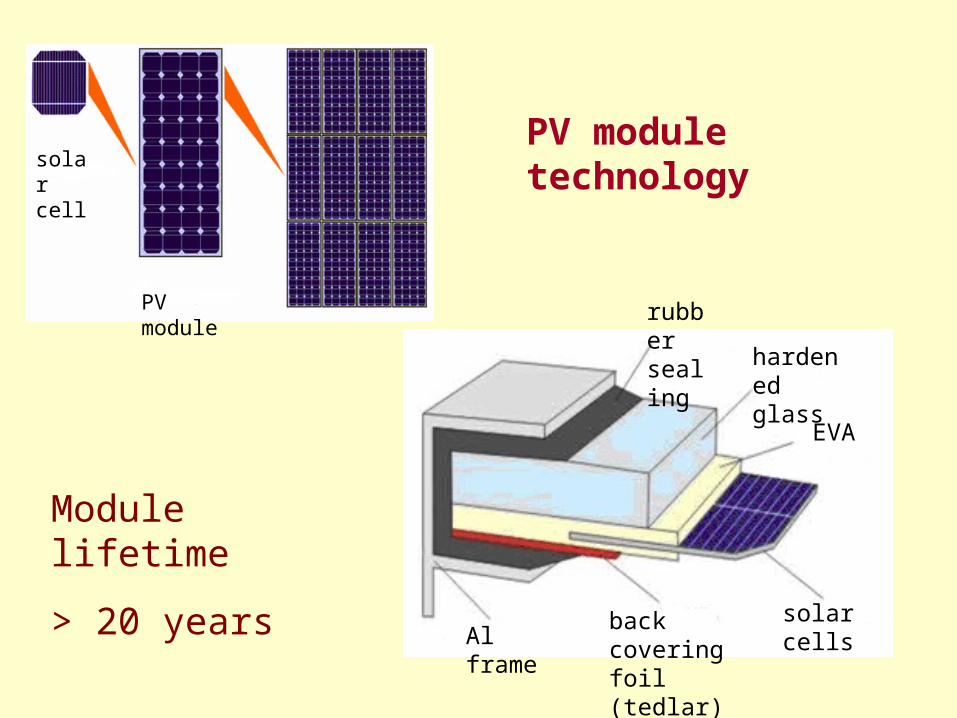
Tandem solar cell – „micromorph“ (microcrystal + amorphous)

Differences between crystalline Si cells and thin film cells
Crystalline Si thin film
structure n+-p(-p+) p+-i-n+
FS contact „fingers and busbars“ all-area TCO contact
thickness 300 m 0.3 až 3 m
BS contact „not important“ back reflector
antireflection texturing TCO light trapping effect
Illumination from „n+- side“ from „p+- side“
Technology n+-diffusion into substrate plasmatic processes
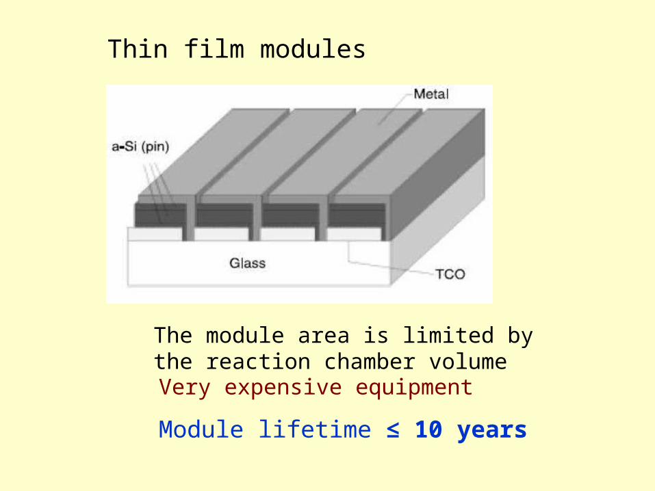
Thin film modules
The module area is limited by the reaction chamber volumeVery expensive equipment
Module lifetime ≤ 10 years


Present market development


0,01
0,1
1
10
100
10 100 1000 10000 100000
Cumulative Quantity Produced
Pri
ce
pe
r U
nit
Slope of Scale-Up: Half the Cost with 10 times more Volume
2002
1
2
3
Implementation Progr.
Technology Transfer
Research & Dev
Funding Mechanisms as driver
Crystalline Si
Thin Films
High Eta, Lowest Cost

Fabrication step A B C
Ingot growing 0,37 0,37 0,73
Wafering 0,00 0,29 0,24
Solar cell fab. 0,15 0,15 0,19
Module fab. 0,43 0,40 0,37
Factory Cost 0,95 1,21 1,53
Manufacuring cost in EUR/Wp for different crystalline Si manufacturing for production of 500 MWp per year
A silicon ribbonB multicrystaline SiC monocrystalline Si

Concentrator systems
The Sun tracking is necessary
heatsink
cells
parabolic mirror

Reliability problems• Environmental effect and aging results in a decrease of
efficiency– a decrease of glass transparency
– an increase of series resistance
– degradation of individual layers of the cell structure
A target: increase module lifetime > 30 years

900 kWh/m2
1800 kWh/m2