Embed Size (px)
Citation preview

CH
G
DS
G
BAT
PA
CK
VC
C
VC4
VC3
VC2
VC1
VSS SRNSRP
PACK+
PACK–
PRES
SMBC
SMBDSMBD
SMBCPBI
TS1 TS2
FU
SE LEDCNTLA
LEDCNTLB
DISP
PT
C
LEDCNTLC
TS3 TS4 BTP
BTP
VC1
VC2
VC3OUT
VDD
GND
2n
dle
ve
l
pro
tec
tor
Cell 1
Cell 2
Cell 3
PRES
PC
HG
Product
Folder
Sample &Buy
Technical
Documents
Tools &
Software
Support &Community
bq40z50SLUSBS8A –DECEMBER 2013–REVISED DECEMBER 2014
bq40z50 1-Series, 2-Series, 3-Series, and 4-Series Li-Ion Battery Pack Manager1 Features 3 Description
The bq40z50 device, incorporating patented1• Fully Integrated 1-Series, 2-Series, 3-Series, and
Impedance Track™ technology, is a fully integrated,4-Series Li-Ion or Li-Polymer Cell Battery Packsingle-chip, pack-based solution that provides a richManager and Protection array of features for gas gauging, protection, and
• Next-Generation Patented Impedance Track™ authentication for 1-series, 2-series, 3-series, and 4-Technology Accurately Measures Available series cell Li-Ion and Li-Polymer battery packs.Charge in Li-Ion and Li-Polymer Batteries
Using its integrated high-performance analog• High Side N-CH Protection FET Drive peripherals, the bq40z50 device measures and• Integrated Cell Balancing While Charging or At maintains an accurate record of available capacity,
voltage, current, temperature, and other criticalRestparameters in Li-Ion or Li-Polymer batteries, and• Full Array of Programmable Protection Featuresreports this information to the system host controller
– Voltage over an SMBus v1.1 compatible interface.– Current
Device Information(1)– Temperature
PART NUMBER PACKAGE BODY SIZE (NOM)– Charge Timeoutbq40z50 VQFN (32) 4.00 mm × 4.00 mm– CHG/DSG FETs
(1) For all available packages, see the orderable addendum at– AFE the end of the datasheet.• Sophisticated Charge Algorithms
Simplified Schematic– JEITA– Enhanced Charging– Adaptive Charging– Cell Balancing
• Supports TURBO BOOST Mode• Supports Battery Trip Point (BTP)• Diagnostic Lifetime Data Monitor and Black Box
Recorder• LED Display• Supports Two-Wire SMBus v1.1 Interface• SHA-1 Authentication• Compact Package: 32-Lead QFN (RSM)
2 Applications• Notebook/Netbook PCs• Medical and Test Equipment• Portable Instrumentation
1
An IMPORTANT NOTICE at the end of this data sheet addresses availability, warranty, changes, use in safety-critical applications,intellectual property matters and other important disclaimers. PRODUCTION DATA.
Not Recommended For New Designs
bq40z50SLUSBS8A –DECEMBER 2013–REVISED DECEMBER 2014 www.ti.com
Table of Contents7.24 Electrical Characteristics: Internal 1.8-V LDO ..... 141 Features .................................................................. 17.25 Electrical Characteristics: High-Frequency2 Applications ........................................................... 1
Oscillator .................................................................. 143 Description ............................................................. 17.26 Electrical Characteristics: Low-Frequency4 Revision History..................................................... 2 Oscillator .................................................................. 15
5 Description (continued)......................................... 3 7.27 Electrical Characteristics: Voltage Reference 1.... 156 Pin Configuration and Functions ......................... 3 7.28 Electrical Characteristics: Voltage Reference 2.... 15
7.29 Electrical Characteristics: Instruction Flash .......... 157 Specifications......................................................... 77.30 Electrical Characteristics: Data Flash ................... 157.1 Absolute Maximum Ratings ...................................... 77.31 Electrical Characteristics: OCD, SCC, SCD1, SCD27.2 ESD Ratings.............................................................. 8
Current Protection Thresholds ................................. 167.3 Recommended Operating Conditions....................... 87.32 Timing Requirements: OCD, SCC, SCD1, SCD27.4 Thermal Information .................................................. 8
Current Protection Timing ........................................ 177.5 Electrical Characteristics: Supply Current................. 97.33 Timing Requirements: SMBus .............................. 177.6 Electrical Characteristics: Power Supply Control...... 97.34 Timing Requirements: SMBus XL......................... 187.7 Electrical Characteristics: AFE Power-On Reset ...... 97.35 Typical Characteristics ......................................... 197.8 Electrical Characteristics: AFE Watchdog Reset and
8 Detailed Description ............................................ 22Wake Timer................................................................ 98.1 Overview ................................................................. 227.9 Electrical Characteristics: Current Wake
Comparator .............................................................. 10 8.2 Functional Block Diagram ...................................... 227.10 Electrical Characteristics: VC1, VC2, VC3, VC4, 8.3 Feature Description................................................. 23
BAT, PACK .............................................................. 10 8.4 Device Functional Modes........................................ 267.11 Electrical Characteristics: SMBD, SMBC.............. 10 9 Applications and Implementation ...................... 277.12 Electrical Characteristics: PRES, BTP_INT, DISP 9.1 Application Information .......................................... 27................................................................................. 10
9.2 Typical Applications ................................................ 287.13 Electrical Characteristics: LEDCNTLA, LEDCNTLB,10 Power Supply Recommendations ..................... 41LEDCNTLC ............................................................. 1111 Layout................................................................... 427.14 Electrical Characteristics: Coulomb Counter ........ 11
11.1 Layout Guidelines ................................................. 427.15 Electrical Characteristics: CC Digital Filter ........... 1111.2 Layout Example .................................................... 447.16 Electrical Characteristics: ADC ............................. 12
7.17 Electrical Characteristics: ADC Digital Filter ......... 12 12 Device and Documentation Support ................. 467.18 Electrical Characteristics: CHG, DSG FET Drive . 12 12.1 Documentation Support ........................................ 467.19 Electrical Characteristics: PCHG FET Drive ......... 13 12.2 Trademarks ........................................................... 467.20 Electrical Characteristics: FUSE Drive.................. 13 12.3 Electrostatic Discharge Caution............................ 467.21 Electrical Characteristics: Internal Temperature 12.4 Glossary ................................................................ 46
Sensor...................................................................... 13 13 Mechanical, Packaging, and Orderable7.22 Electrical Characteristics: TS1, TS2, TS3, TS4 .... 14 Information ........................................................... 467.23 Electrical Characteristics: PTC, PTCEN ............... 14
4 Revision History
Changes from Original (December 2013) to Revision A Page
• Added ESD Ratings table, Feature Description section, Device Functional Modes, Application and Implementationsection, Power Supply Recommendations section, Layout section, Device and Documentation Support section, andMechanical, Packaging, and Orderable Information section ................................................................................................. 1
• Added Feature: Supports TURBO BOOST Mode .................................................................................................................. 1• Added Feature: Supports Battery Trip Point (BTP) ............................................................................................................... 1• Changed a Feature bullet from "Diagnostic Lifetime Data Monitor" to "Diagnostic Lifetime Data Monitor and Black
Box Recorder" ....................................................................................................................................................................... 1• Updated second paragraph of the Description. Added text "The bq40z50 device supports TURBO BOOST mode . . . ".... 3
2 Submit Documentation Feedback Copyright © 2013–2014, Texas Instruments Incorporated
Product Folder Links: bq40z50
Not Recommended For New Designs
1
2VC4
3VC3
4VC2
5VC1
6
VS
S
7
TS
1
8
TS
2
9
TS
3
10
TS
4
11
SRP
12
SRN
13
BT
P_IN
T
19
LEDCNTLC
18
LEDCNTLB
17
LEDCNTLA
16
15
SMBC
22
23
PA
CK
24
DS
G
29
NC
30
CH
G3
1
BA
T3
2
PBI
SMBD
14
21
VC
C
20
FU
SE
PR
ES
or
SH
UT
DN
NC
PC
HG
25
26
27
28
DISP
PTC
PTCEN
NC
¯¯¯¯
¯¯¯¯
¯¯¯¯
bq40z50www.ti.com SLUSBS8A –DECEMBER 2013–REVISED DECEMBER 2014
5 Description (continued)The bq40z50 device supports TURBO BOOST mode by providing the available max power and max current tothe host system. The device also supports Battery Trip Point to send a BTP interrupt signal to the host system atthe pre-set state of charge thresholds.
The bq40z50 provides software-based 1st- and 2nd-level safety protection against overvoltage, undervoltage,overcurrent, short-circuit current, overload, and overtemperature conditions, as well as other pack- and cell-related faults.
SHA-1 authentication, with secure memory for authentication keys, enables identification of genuine batterypacks.
The compact 32-lead QFN package minimizes solution cost and size for smart batteries while providingmaximum functionality and safety for battery gauging applications.
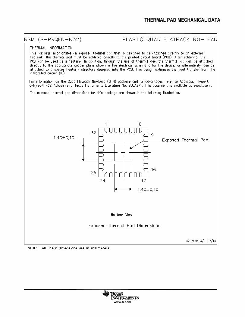
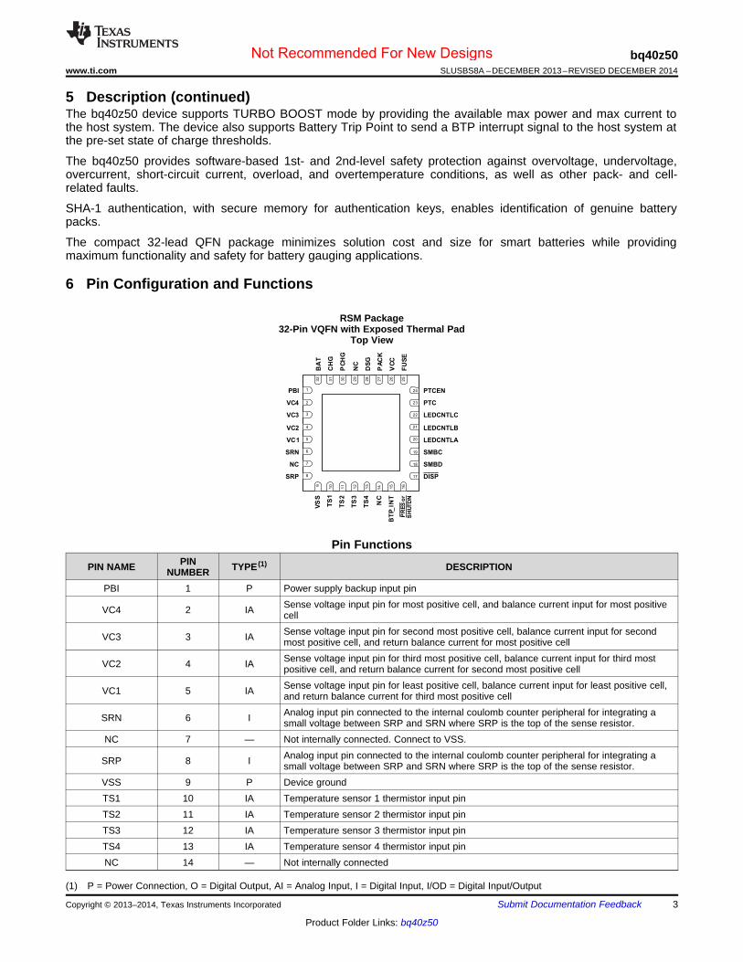
6 Pin Configuration and Functions
RSM Package32-Pin VQFN with Exposed Thermal Pad
Top View
Pin FunctionsPINPIN NAME TYPE (1) DESCRIPTIONNUMBER
PBI 1 P Power supply backup input pinSense voltage input pin for most positive cell, and balance current input for most positiveVC4 2 IA cellSense voltage input pin for second most positive cell, balance current input for secondVC3 3 IA most positive cell, and return balance current for most positive cellSense voltage input pin for third most positive cell, balance current input for third mostVC2 4 IA positive cell, and return balance current for second most positive cellSense voltage input pin for least positive cell, balance current input for least positive cell,VC1 5 IA and return balance current for third most positive cellAnalog input pin connected to the internal coulomb counter peripheral for integrating aSRN 6 I small voltage between SRP and SRN where SRP is the top of the sense resistor.
NC 7 — Not internally connected. Connect to VSS.Analog input pin connected to the internal coulomb counter peripheral for integrating aSRP 8 I small voltage between SRP and SRN where SRP is the top of the sense resistor.
VSS 9 P Device groundTS1 10 IA Temperature sensor 1 thermistor input pinTS2 11 IA Temperature sensor 2 thermistor input pinTS3 12 IA Temperature sensor 3 thermistor input pinTS4 13 IA Temperature sensor 4 thermistor input pinNC 14 — Not internally connected
(1) P = Power Connection, O = Digital Output, AI = Analog Input, I = Digital Input, I/OD = Digital Input/Output
Copyright © 2013–2014, Texas Instruments Incorporated Submit Documentation Feedback 3
Product Folder Links: bq40z50
Not Recommended For New Designs
bq40z50SLUSBS8A –DECEMBER 2013–REVISED DECEMBER 2014 www.ti.com
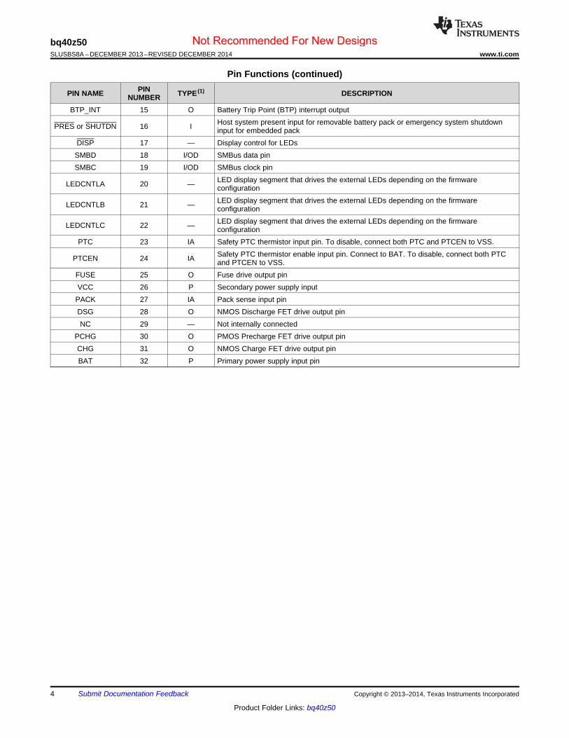
Pin Functions (continued)PINPIN NAME TYPE (1) DESCRIPTIONNUMBER
BTP_INT 15 O Battery Trip Point (BTP) interrupt outputHost system present input for removable battery pack or emergency system shutdownPRES or SHUTDN 16 I input for embedded pack
DISP 17 — Display control for LEDsSMBD 18 I/OD SMBus data pinSMBC 19 I/OD SMBus clock pin
LED display segment that drives the external LEDs depending on the firmwareLEDCNTLA 20 — configurationLED display segment that drives the external LEDs depending on the firmwareLEDCNTLB 21 — configurationLED display segment that drives the external LEDs depending on the firmwareLEDCNTLC 22 — configuration
PTC 23 IA Safety PTC thermistor input pin. To disable, connect both PTC and PTCEN to VSS.Safety PTC thermistor enable input pin. Connect to BAT. To disable, connect both PTCPTCEN 24 IA and PTCEN to VSS.
FUSE 25 O Fuse drive output pinVCC 26 P Secondary power supply input
PACK 27 IA Pack sense input pinDSG 28 O NMOS Discharge FET drive output pinNC 29 — Not internally connected
PCHG 30 O PMOS Precharge FET drive output pinCHG 31 O NMOS Charge FET drive output pinBAT 32 P Primary power supply input pin
4 Submit Documentation Feedback Copyright © 2013–2014, Texas Instruments Incorporated
Product Folder Links: bq40z50
Not Recommended For New Designs
BAT PACKVCC
PBIReference
System1.8 V
Domain
+
– PACK
Detector
BATDET
ENVCC3.1 V
Shutdown
Latch
BAT
Control
ENBAT
PACKDET
SHUTDOWN
SHOUT
BATCHG
Pump
CHG2 kΩ
CHGOFF
CHGEN
BATDSG
Pump
DSG2 kΩ
DSGEN
PACK
DSGOFF
Power Supply Control
CHG, DSG Drive
PCHG2 kΩ
VCC
PCHGEN
8 kΩ
Pre-Charge Drive
VCC
Zero-Volt Charge
BATCHG
Pump
CHGEN
BATZVCD
ZVCHGEN
Cell Balancing
VC1
VC2
VC3
VC4
CDEN4
CDEN3
CDEN2
CDEN1
ADC Mux ADC
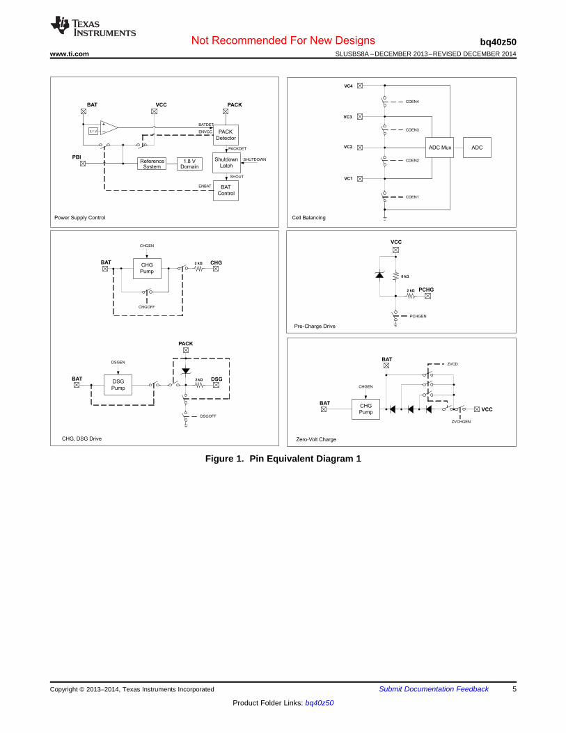
bq40z50www.ti.com SLUSBS8A –DECEMBER 2013–REVISED DECEMBER 2014
Figure 1. Pin Equivalent Diagram 1
Copyright © 2013–2014, Texas Instruments Incorporated Submit Documentation Feedback 5
Product Folder Links: bq40z50
Not Recommended For New Designs

SMBus Interface
100 kΩ
1 MΩ
SMBC
SMBCIN
SMBCENSMBCOUT
100 kΩ
1 MΩ
SMBDSMBDIN
SMBDENSMBDOUT
FUSE
2 kΩ
FUSE Drive
FUSEEN
BATFUSEWKPUP
100 kΩ FUSEDIG
150 nA
Thermistor Inputs
ADTHx
2 kΩ
TS1,2,3,4
18 kΩ
1.8 V
ADC Mux
High-Voltage GPIO
RHOEN
PBI
100 kΩ
RHIN
10 kΩ
PRES
RHOUT
LED Drive
RLOEN
BAT
100 kΩ
RLIN
10 kΩ
LED1, 2, 3
RLOUT
22.5 mA
ADC
PTCPTC
Counter
PTC
Latch
PTCDIG
290 nA
PTCEN
30 kΩPTC
Comparator
PTC Detection
RCWKPUP
1 kΩ RCIN
RCOUT
1.8 V
RCPUP
1.8 V
bq40z50SLUSBS8A –DECEMBER 2013–REVISED DECEMBER 2014 www.ti.com
Figure 2. Pin Equivalent Diagram 2
6 Submit Documentation Feedback Copyright © 2013–2014, Texas Instruments Incorporated
Product Folder Links: bq40z50
Not Recommended For New Designs
VC and PACK Dividers
CHANx
1.9 MΩ
VC4
0.1 MΩ
10 Ω
ADC Mux ADC
CHANx
1.9 MΩ
PACK
0.1 MΩ
10 Ω
ADC Mux ADC
OCD, SCC, SCD Comparators and Coulomb Counter
SRP
SRN
3.8 kΩ
3.8 kΩ
Comparator
Array
100 Ω
100 Ω
Coulomb
Counter
Φ2
Φ1
Φ2
Φ1
Φ2
Φ1
Φ2
Φ1
4
bq40z50www.ti.com SLUSBS8A –DECEMBER 2013–REVISED DECEMBER 2014
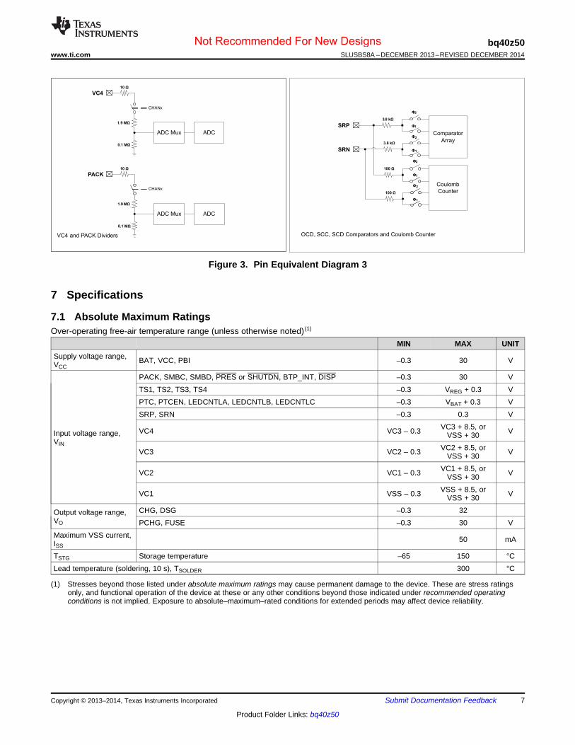
Figure 3. Pin Equivalent Diagram 3
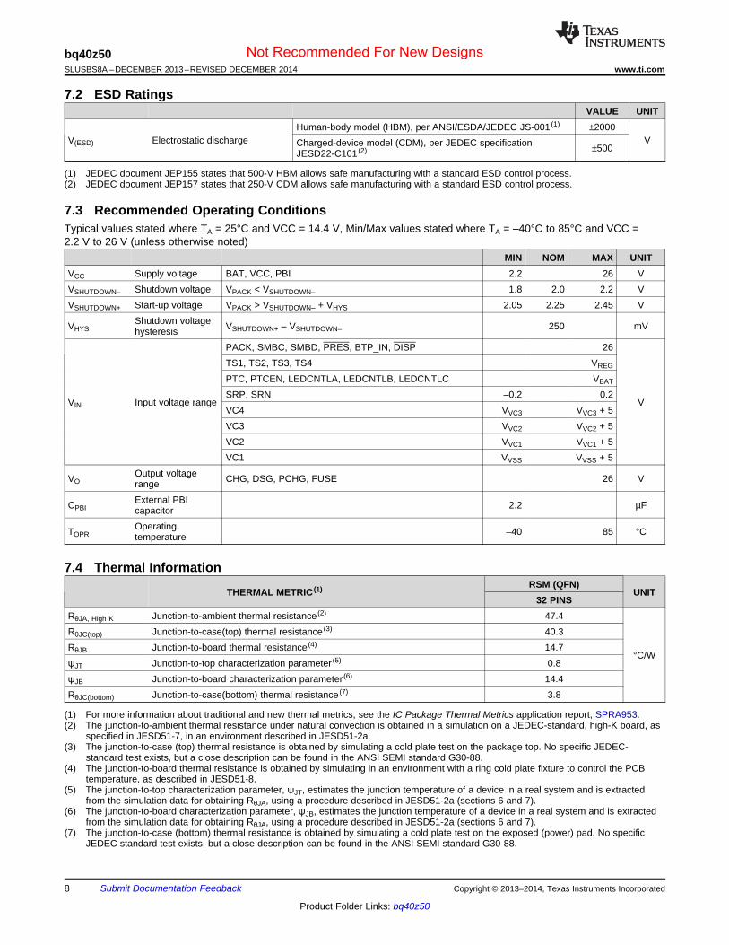
7 Specifications
7.1 Absolute Maximum RatingsOver-operating free-air temperature range (unless otherwise noted) (1)
MIN MAX UNITSupply voltage range, BAT, VCC, PBI –0.3 30 VVCC
PACK, SMBC, SMBD, PRES or SHUTDN, BTP_INT, DISP –0.3 30 VTS1, TS2, TS3, TS4 –0.3 VREG + 0.3 VPTC, PTCEN, LEDCNTLA, LEDCNTLB, LEDCNTLC –0.3 VBAT + 0.3 VSRP, SRN –0.3 0.3 V
VC3 + 8.5, orVC4 VC3 – 0.3 VInput voltage range, VSS + 30VIN VC2 + 8.5, orVC3 VC2 – 0.3 VVSS + 30
VC1 + 8.5, orVC2 VC1 – 0.3 VVSS + 30VSS + 8.5, orVC1 VSS – 0.3 VVSS + 30
CHG, DSG –0.3 32Output voltage range,VO PCHG, FUSE –0.3 30 VMaximum VSS current, 50 mAISS
TSTG Storage temperature –65 150 °CLead temperature (soldering, 10 s), TSOLDER 300 °C
(1) Stresses beyond those listed under absolute maximum ratings may cause permanent damage to the device. These are stress ratingsonly, and functional operation of the device at these or any other conditions beyond those indicated under recommended operatingconditions is not implied. Exposure to absolute–maximum–rated conditions for extended periods may affect device reliability.
Copyright © 2013–2014, Texas Instruments Incorporated Submit Documentation Feedback 7
Product Folder Links: bq40z50
Not Recommended For New Designs
bq40z50SLUSBS8A –DECEMBER 2013–REVISED DECEMBER 2014 www.ti.com
7.2 ESD RatingsVALUE UNIT
Human-body model (HBM), per ANSI/ESDA/JEDEC JS-001 (1) ±2000V(ESD) Electrostatic discharge VCharged-device model (CDM), per JEDEC specification ±500JESD22-C101 (2)
(1) JEDEC document JEP155 states that 500-V HBM allows safe manufacturing with a standard ESD control process.(2) JEDEC document JEP157 states that 250-V CDM allows safe manufacturing with a standard ESD control process.
7.3 Recommended Operating ConditionsTypical values stated where TA = 25°C and VCC = 14.4 V, Min/Max values stated where TA = –40°C to 85°C and VCC =2.2 V to 26 V (unless otherwise noted)
MIN NOM MAX UNITVCC Supply voltage BAT, VCC, PBI 2.2 26 VVSHUTDOWN– Shutdown voltage VPACK < VSHUTDOWN– 1.8 2.0 2.2 VVSHUTDOWN+ Start-up voltage VPACK > VSHUTDOWN– + VHYS 2.05 2.25 2.45 V
Shutdown voltageVHYS VSHUTDOWN+ – VSHUTDOWN– 250 mVhysteresisPACK, SMBC, SMBD, PRES, BTP_IN, DISP 26TS1, TS2, TS3, TS4 VREG
PTC, PTCEN, LEDCNTLA, LEDCNTLB, LEDCNTLC VBAT
SRP, SRN –0.2 0.2VIN Input voltage range V
VC4 VVC3 VVC3 + 5VC3 VVC2 VVC2 + 5VC2 VVC1 VVC1 + 5VC1 VVSS VVSS + 5
Output voltageVO CHG, DSG, PCHG, FUSE 26 VrangeExternal PBICPBI 2.2 µFcapacitorOperatingTOPR –40 85 °Ctemperature
7.4 Thermal InformationRSM (QFN)
THERMAL METRIC (1) UNIT32 PINS
RθJA, High K Junction-to-ambient thermal resistance (2) 47.4RθJC(top) Junction-to-case(top) thermal resistance (3) 40.3RθJB Junction-to-board thermal resistance (4) 14.7
°C/WψJT Junction-to-top characterization parameter (5) 0.8ψJB Junction-to-board characterization parameter (6) 14.4RθJC(bottom) Junction-to-case(bottom) thermal resistance (7) 3.8
(1) For more information about traditional and new thermal metrics, see the IC Package Thermal Metrics application report, SPRA953.(2) The junction-to-ambient thermal resistance under natural convection is obtained in a simulation on a JEDEC-standard, high-K board, as
specified in JESD51-7, in an environment described in JESD51-2a.(3) The junction-to-case (top) thermal resistance is obtained by simulating a cold plate test on the package top. No specific JEDEC-
standard test exists, but a close description can be found in the ANSI SEMI standard G30-88.(4) The junction-to-board thermal resistance is obtained by simulating in an environment with a ring cold plate fixture to control the PCB
temperature, as described in JESD51-8.(5) The junction-to-top characterization parameter, ψJT, estimates the junction temperature of a device in a real system and is extracted
from the simulation data for obtaining RθJA, using a procedure described in JESD51-2a (sections 6 and 7).(6) The junction-to-board characterization parameter, ψJB, estimates the junction temperature of a device in a real system and is extracted
from the simulation data for obtaining RθJA, using a procedure described in JESD51-2a (sections 6 and 7).(7) The junction-to-case (bottom) thermal resistance is obtained by simulating a cold plate test on the exposed (power) pad. No specific
JEDEC standard test exists, but a close description can be found in the ANSI SEMI standard G30-88.Spacer
8 Submit Documentation Feedback Copyright © 2013–2014, Texas Instruments Incorporated
Product Folder Links: bq40z50
Not Recommended For New Designs
bq40z50www.ti.com SLUSBS8A –DECEMBER 2013–REVISED DECEMBER 2014
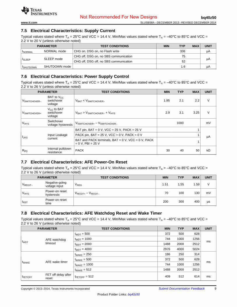
7.5 Electrical Characteristics: Supply CurrentTypical values stated where TA = 25°C and VCC = 14.4 V, Min/Max values stated where TA = –40°C to 85°C and VCC =2.2 V to 20 V (unless otherwise noted)
PARAMETER TEST CONDITIONS MIN TYP MAX UNITINORMAL NORMAL mode CHG on. DSG on, no Flash write 336 µA
CHG off, DSG on, no SBS communication 75ISLEEP SLEEP mode µA
CHG off, DSG off, no SBS communication 52ISHUTDOWN SHUTDOWN mode 1.6 µA
7.6 Electrical Characteristics: Power Supply ControlTypical values stated where TA = 25°C and VCC = 14.4 V, Min/Max values stated where TA = –40°C to 85°C and VCC =2.2 V to 26 V (unless otherwise noted)
PARAMETER TEST CONDITIONS MIN TYP MAX UNITBAT to VCC
VSWITCHOVER– switchover VBAT < VSWITCHOVER– 1.95 2.1 2.2 VvoltageVCC to BAT
VSWITCHOVER+ switchover VBAT > VSWITCHOVER– + VHYS 2.9 3.1 3.25 VvoltageSwitchoverVHYS VSWITCHOVER+ – VSWITCHOVER– 1000 mVvoltage hysteresis
BAT pin, BAT = 0 V, VCC = 25 V, PACK = 25 V 1Input Leakage PACK pin, BAT = 25 V, VCC = 0 V, PACK = 0 V 1ILKG µAcurrent BAT and PACK terminals, BAT = 0 V, VCC = 0 V, PACK 1= 0 V, PBI = 25 VInternal pulldownRPD PACK 30 40 50 kΩresistance
7.7 Electrical Characteristics: AFE Power-On ResetTypical values stated where TA = 25°C and VCC = 14.4 V, Min/Max values stated where TA = –40°C to 85°C and VCC =2.2 V to 26 V (unless otherwise noted)
PARAMETER TEST CONDITIONS MIN TYP MAX UNITNegative-goingVREGIT– VREG 1.51 1.55 1.59 Vvoltage inputPower-on resetVHYS VREGIT+ – VREGIT– 70 100 130 mVhysteresisPower-on resettRST 200 300 400 µstime
7.8 Electrical Characteristics: AFE Watchdog Reset and Wake TimerTypical values stated where TA = 25°C and VCC = 14.4 V, Min/Max values stated where TA = –40°C to 85°C and VCC =2.2 V to 26 V (unless otherwise noted)
PARAMETER TEST CONDITIONS MIN TYP MAX UNITtWDT = 500 372 500 628tWDT = 1000 744 1000 1256AFE watchdogtWDT mstimeout tWDT = 2000 1488 2000 2512tWDT = 4000 2976 4000 5024tWAKE = 250 186 250 314tWAKE = 500 372 500 628
tWAKE AFE wake timer mstWAKE = 1000 744 1000 1256tWAKE = 512 1488 2000 2512
FET off delay aftertFETOFF tFETOFF = 512 409 512 614 msreset
Copyright © 2013–2014, Texas Instruments Incorporated Submit Documentation Feedback 9
Product Folder Links: bq40z50
Not Recommended For New Designs
bq40z50SLUSBS8A –DECEMBER 2013–REVISED DECEMBER 2014 www.ti.com
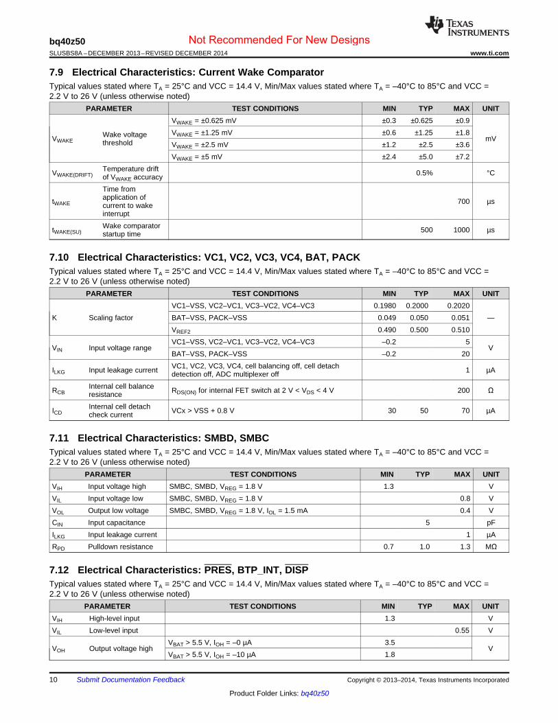
7.9 Electrical Characteristics: Current Wake ComparatorTypical values stated where TA = 25°C and VCC = 14.4 V, Min/Max values stated where TA = –40°C to 85°C and VCC =2.2 V to 26 V (unless otherwise noted)
PARAMETER TEST CONDITIONS MIN TYP MAX UNITVWAKE = ±0.625 mV ±0.3 ±0.625 ±0.9VWAKE = ±1.25 mV ±0.6 ±1.25 ±1.8Wake voltageVWAKE mVthreshold VWAKE = ±2.5 mV ±1.2 ±2.5 ±3.6VWAKE = ±5 mV ±2.4 ±5.0 ±7.2
Temperature driftVWAKE(DRIFT) 0.5% °Cof VWAKE accuracyTime fromapplication oftWAKE 700 µscurrent to wakeinterruptWake comparatortWAKE(SU) 500 1000 µsstartup time
7.10 Electrical Characteristics: VC1, VC2, VC3, VC4, BAT, PACKTypical values stated where TA = 25°C and VCC = 14.4 V, Min/Max values stated where TA = –40°C to 85°C and VCC =2.2 V to 26 V (unless otherwise noted)
PARAMETER TEST CONDITIONS MIN TYP MAX UNITVC1–VSS, VC2–VC1, VC3–VC2, VC4–VC3 0.1980 0.2000 0.2020
K Scaling factor BAT–VSS, PACK–VSS 0.049 0.050 0.051 —VREF2 0.490 0.500 0.510VC1–VSS, VC2–VC1, VC3–VC2, VC4–VC3 –0.2 5
VIN Input voltage range VBAT–VSS, PACK–VSS –0.2 20VC1, VC2, VC3, VC4, cell balancing off, cell detachILKG Input leakage current 1 µAdetection off, ADC multiplexer off
Internal cell balanceRCB RDS(ON) for internal FET switch at 2 V < VDS < 4 V 200 ΩresistanceInternal cell detachICD VCx > VSS + 0.8 V 30 50 70 µAcheck current
7.11 Electrical Characteristics: SMBD, SMBCTypical values stated where TA = 25°C and VCC = 14.4 V, Min/Max values stated where TA = –40°C to 85°C and VCC =2.2 V to 26 V (unless otherwise noted)
PARAMETER TEST CONDITIONS MIN TYP MAX UNITVIH Input voltage high SMBC, SMBD, VREG = 1.8 V 1.3 VVIL Input voltage low SMBC, SMBD, VREG = 1.8 V 0.8 VVOL Output low voltage SMBC, SMBD, VREG = 1.8 V, IOL = 1.5 mA 0.4 VCIN Input capacitance 5 pFILKG Input leakage current 1 µARPD Pulldown resistance 0.7 1.0 1.3 MΩ
7.12 Electrical Characteristics: PRES, BTP_INT, DISPTypical values stated where TA = 25°C and VCC = 14.4 V, Min/Max values stated where TA = –40°C to 85°C and VCC =2.2 V to 26 V (unless otherwise noted)
PARAMETER TEST CONDITIONS MIN TYP MAX UNITVIH High-level input 1.3 VVIL Low-level input 0.55 V
VBAT > 5.5 V, IOH = –0 µA 3.5VOH Output voltage high V
VBAT > 5.5 V, IOH = –10 µA 1.8
10 Submit Documentation Feedback Copyright © 2013–2014, Texas Instruments Incorporated
Product Folder Links: bq40z50
Not Recommended For New Designs

bq40z50www.ti.com SLUSBS8A –DECEMBER 2013–REVISED DECEMBER 2014
Electrical Characteristics: PRES, BTP_INT, DISP (continued)Typical values stated where TA = 25°C and VCC = 14.4 V, Min/Max values stated where TA = –40°C to 85°C and VCC =2.2 V to 26 V (unless otherwise noted)
PARAMETER TEST CONDITIONS MIN TYP MAX UNITVOL Output voltage low IOL = 1.5 mA 0.4 VCIN Input capacitance 5 pFILKG Input leakage current 1 µA
Output reverseRO Between PRES or BTP_INT or DISP and PBI 8 kΩresistance
7.13 Electrical Characteristics: LEDCNTLA, LEDCNTLB, LEDCNTLCTypical values stated where TA = 25°C and VCC = 14.4 V, Min/Max values stated where TA = –40°C to 85°C and VCC =2.2 V to 26 V (unless otherwise noted)
PARAMETER TEST CONDITIONS MIN TYP MAX UNITVIH High-level input 1.45 VVIL Low-level input 0.55 V
VBAT –VOH Output voltage high VBAT > 3.0 V, IOH = –22.5 mA V1.6VOL Output voltage low IOL = 1.5 mA 0.4 V
High level outputISC –30 –45 –6 0 mAcurrent protectionLow level outputIOL VBAT > 3.0 V, VOH = 0.4 V 15.75 22.5 29.25 mAcurrentCurrent matchingILEDCNTLx VBAT = VLEDCNTLx + 2.5 V ±1%between LEDCNTLx
CIN Input capacitance 20 pFILKG Input leakage current 1 µA
Frequency of LEDfLEDCNTLx 124 Hzpattern
7.14 Electrical Characteristics: Coulomb CounterTypical values stated where TA = 25°C and VCC = 14.4 V, Min/Max values stated where TA = –40°C to 85°C and VCC =2.2 V to 26 V (unless otherwise noted)
PARAMETER TEST CONDITIONS MIN TYP MAX UNITInput voltage range –0.1 0.1 VFull scale range –VREF1/10 VREF1/10 VIntegral nonlinearity (1) 16-bit, best fit over input voltage range ±5.2 ±22.3 LSBOffset error 16-bit, Post-calibration ±5 ±10 µVOffset error drift 15-bit + sign, Post-calibration 0.2 0.3 µV/°CGain error 15-bit + sign, over input voltage range ±0.2% ±0.8% FSRGain error drift 15-bit + sign, over input voltage range 150 PPM/°CEffective input resistance 2.5 MΩ
(1) 1 LSB = VREF1/(10 × 2N) = 1.215/(10 × 215) = 3.71 µV
7.15 Electrical Characteristics: CC Digital FilterTypical values stated where TA = 25°C and VCC = 14.4 V, Min/Max values stated where TA = –40°C to 85°C and VCC =2.2 V to 26 V (unless otherwise noted)
PARAMETER TEST CONDITIONS MIN TYP MAX UNITConversion time Single conversion 250 msEffective resolution Single conversion 15 Bits
Copyright © 2013–2014, Texas Instruments Incorporated Submit Documentation Feedback 11
Product Folder Links: bq40z50
Not Recommended For New Designs

bq40z50SLUSBS8A –DECEMBER 2013–REVISED DECEMBER 2014 www.ti.com
7.16 Electrical Characteristics: ADCTypical values stated where TA = 25°C and VCC = 14.4 V, Min/Max values stated where TA = –40°C to 85°C and VCC =2.2 V to 26 V (unless otherwise noted)
PARAMETER TEST CONDITIONS MIN TYP MAX UNITInternal reference (VREF1) –0.2 1
Input voltage range VExternal reference (VREG) –0.2 0.8 x VREG
Full scale range VFS = VREF1 or VREG –VFS VFS V16-bit, best fit, –0.1 V to 0.8 x VREF1 ±6.6
Integral nonlinearity (1) LSB16-bit, best fit, –0.2 V to –0.1 V ±13.1
Offset error (2) 16-bit, Post-calibration, VFS = VREF1 ±67 ±157 µVOffset error drift 16-bit, Post-calibration, VFS = VREF1 0.6 3 µV/°CGain error 16-bit, –0.1 V to 0.8 x VFS ±0.2% ±0.8% FSRGain error drift 16-bit, –0.1 V to 0.8 x VFS 150 PPM/°CEffective input resistance 8 MΩ
(1) 1 LSB = VREF1/(2N) = 1.225/(215) = 37.4 µV (when tCONV = 31.25 ms)(2) For VC1–VSS, VC2–VC1, VC3–VC2, VC4–VC3, VC4–VSS, PACK–VSS, and VREF1/2, the offset error is multiplied by (1/ADC
multiplexer scaling factor (K)).
7.17 Electrical Characteristics: ADC Digital FilterTypical values stated where TA = 25°C and VCC = 14.4 V, Min/Max values stated where TA = –40°C to 85°C and VCC =2.2 V to 26 V (unless otherwise noted)
PARAMETER TEST CONDITIONS MIN TYP MAX UNITSingle conversion 31.25Single conversion 15.63
Conversion time msSingle conversion 7.81Single conversion 1.95
Resolution No missing codes 16 BitsWith sign, tCONV = 31.25 ms 14 15With sign, tCONV = 15.63 ms 13 14
Effective resolution BitsWith sign, tCONV = 7.81 ms 11 12With sign, tCONV = 1.95 ms 9 10
7.18 Electrical Characteristics: CHG, DSG FET DriveTypical values stated where TA = 25°C and VCC = 14.4 V, Min/Max values stated where TA = –40°C to 85°C and VCC =2.2 V to 26 V (unless otherwise noted)
PARAMETER TEST CONDITIONS MIN TYP MAX UNITRatioDSG = (VDSG – VBAT)/VBAT, 2.2 V < VBAT < 4.92 V, 2.133 2.333 2.43310 MΩ between PACK and DSGOutput voltage —ratio RatioCHG = (VCHG – VBAT)/VBAT, 2.2 V < VBAT < 4.92 V, 2.133 2.333 2.43310 MΩ between BAT and CHGVDSG(ON) = VDSG – VBAT, VBAT ≥ 4.92 V, 10 MΩ between 10.5 11.5 12PACK and DSG, VBAT = 18 VOutput voltage,V(FETON) VCHG and DSG on VCHG(ON) = VCHG – VBAT, VBAT ≥ 4.92 V, 10 MΩ between 10.5 11.5 12BAT and CHG, VBAT = 18 VVDSG(OFF) = VDSG – VPACK, 10 MΩ between PACK and –0.4 0.4Output voltage, DSGV(FETOFF) VCHG and DSG offVCHG(OFF) = VCHG – VBAT, 10 MΩ between BAT and CHG –0.4 0.4VDSG from 0% to 35% VDSG(ON)(TYP), VBAT ≥ 2.2 V, CL =4.7 nF between DSG and PACK, 5.1 kΩ between DSG 200 500and CL, 10 MΩ between PACK and DSG
tR Rise time µsVCHG from 0% to 35% VCHG(ON)(TYP), VBAT ≥ 2.2 V, CL =4.7 nF between CHG and BAT, 5.1 kΩ between CHG 200 500and CL, 10 MΩ between BAT and CHG
12 Submit Documentation Feedback Copyright © 2013–2014, Texas Instruments Incorporated
Product Folder Links: bq40z50
Not Recommended For New Designs
bq40z50www.ti.com SLUSBS8A –DECEMBER 2013–REVISED DECEMBER 2014
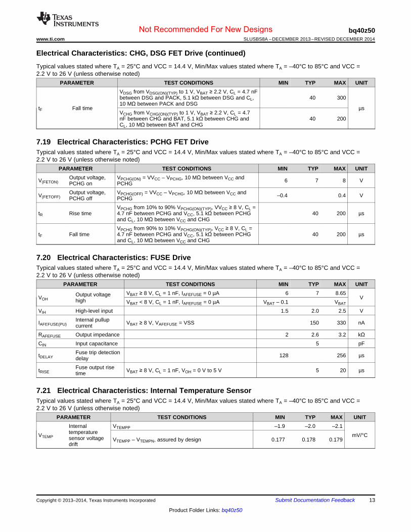
Electrical Characteristics: CHG, DSG FET Drive (continued)Typical values stated where TA = 25°C and VCC = 14.4 V, Min/Max values stated where TA = –40°C to 85°C and VCC =2.2 V to 26 V (unless otherwise noted)
PARAMETER TEST CONDITIONS MIN TYP MAX UNITVDSG from VDSG(ON)(TYP) to 1 V, VBAT ≥ 2.2 V, CL = 4.7 nFbetween DSG and PACK, 5.1 kΩ between DSG and CL, 40 30010 MΩ between PACK and DSG
tF Fall time µsVCHG from VCHG(ON)(TYP) to 1 V, VBAT ≥ 2.2 V, CL = 4.7nF between CHG and BAT, 5.1 kΩ between CHG and 40 200CL, 10 MΩ between BAT and CHG
7.19 Electrical Characteristics: PCHG FET DriveTypical values stated where TA = 25°C and VCC = 14.4 V, Min/Max values stated where TA = –40°C to 85°C and VCC =2.2 V to 26 V (unless otherwise noted)
PARAMETER TEST CONDITIONS MIN TYP MAX UNITOutput voltage, VPCHG(ON) = VVCC – VPCHG, 10 MΩ between VCC andV(FETON) 6 7 8 VPCHG on PCHGOutput voltage, VPCHG(OFF) = VVCC – VPCHG, 10 MΩ between VCC andV(FETOFF) –0.4 0.4 VPCHG off PCHG
VPCHG from 10% to 90% VPCHG(ON)(TYP), VVCC ≥ 8 V, CL =tR Rise time 4.7 nF between PCHG and VCC, 5.1 kΩ between PCHG 40 200 µs
and CL, 10 MΩ between VCC and CHGVPCHG from 90% to 10% VPCHG(ON)(TYP), VCC ≥ 8 V, CL =
tF Fall time 4.7 nF between PCHG and VCC, 5.1 kΩ between PCHG 40 200 µsand CL, 10 MΩ between VCC and CHG
7.20 Electrical Characteristics: FUSE DriveTypical values stated where TA = 25°C and VCC = 14.4 V, Min/Max values stated where TA = –40°C to 85°C and VCC =2.2 V to 26 V (unless otherwise noted)
PARAMETER TEST CONDITIONS MIN TYP MAX UNITVBAT ≥ 8 V, CL = 1 nF, IAFEFUSE = 0 µA 6 7 8.65Output voltageVOH Vhigh VBAT < 8 V, CL = 1 nF, IAFEFUSE = 0 µA VBAT – 0.1 VBAT
VIH High-level input 1.5 2.0 2.5 VInternal pullupIAFEFUSE(PU) VBAT ≥ 8 V, VAFEFUSE = VSS 150 330 nAcurrent
RAFEFUSE Output impedance 2 2.6 3.2 kΩCIN Input capacitance 5 pF
Fuse trip detectiontDELAY 128 256 µsdelayFuse output risetRISE VBAT ≥ 8 V, CL = 1 nF, VOH = 0 V to 5 V 5 20 µstime
7.21 Electrical Characteristics: Internal Temperature SensorTypical values stated where TA = 25°C and VCC = 14.4 V, Min/Max values stated where TA = –40°C to 85°C and VCC =2.2 V to 26 V (unless otherwise noted)
PARAMETER TEST CONDITIONS MIN TYP MAX UNITInternal VTEMPP –1.9 –2.0 –2.1temperatureVTEMP mV/°Csensor voltage VTEMPP – VTEMPN, assured by design 0.177 0.178 0.179drift
Copyright © 2013–2014, Texas Instruments Incorporated Submit Documentation Feedback 13
Product Folder Links: bq40z50
Not Recommended For New Designs
bq40z50SLUSBS8A –DECEMBER 2013–REVISED DECEMBER 2014 www.ti.com
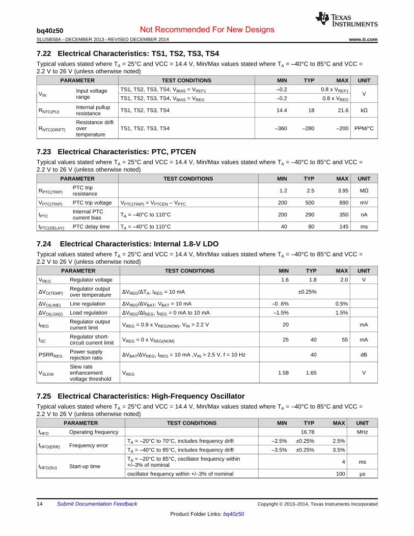
7.22 Electrical Characteristics: TS1, TS2, TS3, TS4Typical values stated where TA = 25°C and VCC = 14.4 V, Min/Max values stated where TA = –40°C to 85°C and VCC =2.2 V to 26 V (unless otherwise noted)
PARAMETER TEST CONDITIONS MIN TYP MAX UNITTS1, TS2, TS3, TS4, VBIAS = VREF1 –0.2 0.8 x VREF1Input voltageVIN Vrange TS1, TS2, TS3, TS4, VBIAS = VREG –0.2 0.8 x VREG
Internal pullupRNTC(PU) TS1, TS2, TS3, TS4 14.4 18 21.6 kΩresistanceResistance drift
RNTC(DRIFT) over TS1, TS2, TS3, TS4 –360 –280 –200 PPM/°Ctemperature
7.23 Electrical Characteristics: PTC, PTCENTypical values stated where TA = 25°C and VCC = 14.4 V, Min/Max values stated where TA = –40°C to 85°C and VCC =2.2 V to 26 V (unless otherwise noted)
PARAMETER TEST CONDITIONS MIN TYP MAX UNITPTC tripRPTC(TRIP) 1.2 2.5 3.95 MΩresistance
VPTC(TRIP) PTC trip voltage VPTC(TRIP) = VPTCEN – VPTC 200 500 890 mVInternal PTCIPTC TA = –40°C to 110°C 200 290 350 nAcurrent bias
tPTC(DELAY) PTC delay time TA = –40°C to 110°C 40 80 145 ms
7.24 Electrical Characteristics: Internal 1.8-V LDOTypical values stated where TA = 25°C and VCC = 14.4 V, Min/Max values stated where TA = –40°C to 85°C and VCC =2.2 V to 26 V (unless otherwise noted)
PARAMETER TEST CONDITIONS MIN TYP MAX UNITVREG Regulator voltage 1.6 1.8 2.0 V
Regulator outputΔVO(TEMP) ΔVREG/ΔTA, IREG = 10 mA ±0.25%over temperatureΔVO(LINE) Line regulation ΔVREG/ΔVBAT, VBAT = 10 mA –0 .6% 0.5%ΔVO(LOAD) Load regulation ΔVREG/ΔIREG, IREG = 0 mA to 10 mA –1.5% 1.5%
Regulator outputIREG VREG = 0.9 x VREG(NOM), VIN > 2.2 V 20 mAcurrent limitRegulator short-ISC VREG = 0 x VREG(NOM) 25 40 55 mAcircuit current limitPower supplyPSRRREG ΔVBAT/ΔVREG, IREG = 10 mA ,VIN > 2.5 V, f = 10 Hz 40 dBrejection ratioSlew rate
VSLEW enhancement VREG 1.58 1.65 Vvoltage threshold
7.25 Electrical Characteristics: High-Frequency OscillatorTypical values stated where TA = 25°C and VCC = 14.4 V, Min/Max values stated where TA = –40°C to 85°C and VCC =2.2 V to 26 V (unless otherwise noted)
PARAMETER TEST CONDITIONS MIN TYP MAX UNITfHFO Operating frequency 16.78 MHz
TA = –20°C to 70°C, includes frequency drift –2.5% ±0.25% 2.5%fHFO(ERR) Frequency error
TA = –40°C to 85°C, includes frequency drift –3.5% ±0.25% 3.5%TA = –20°C to 85°C, oscillator frequency within 4 ms+/–3% of nominaltHFO(SU) Start-up timeoscillator frequency within +/–3% of nominal 100 µs
14 Submit Documentation Feedback Copyright © 2013–2014, Texas Instruments Incorporated
Product Folder Links: bq40z50
Not Recommended For New Designs
bq40z50www.ti.com SLUSBS8A –DECEMBER 2013–REVISED DECEMBER 2014
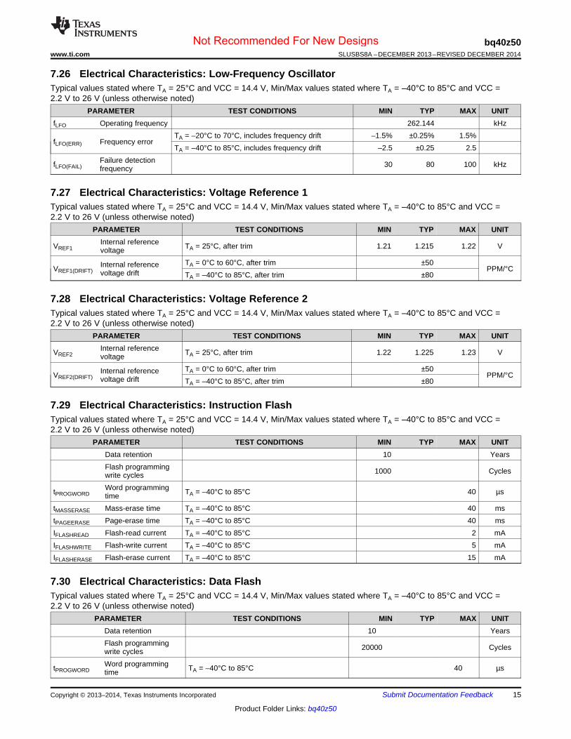
7.26 Electrical Characteristics: Low-Frequency OscillatorTypical values stated where TA = 25°C and VCC = 14.4 V, Min/Max values stated where TA = –40°C to 85°C and VCC =2.2 V to 26 V (unless otherwise noted)
PARAMETER TEST CONDITIONS MIN TYP MAX UNITfLFO Operating frequency 262.144 kHz
TA = –20°C to 70°C, includes frequency drift –1.5% ±0.25% 1.5%fLFO(ERR) Frequency error
TA = –40°C to 85°C, includes frequency drift –2.5 ±0.25 2.5Failure detectionfLFO(FAIL) 30 80 100 kHzfrequency
7.27 Electrical Characteristics: Voltage Reference 1Typical values stated where TA = 25°C and VCC = 14.4 V, Min/Max values stated where TA = –40°C to 85°C and VCC =2.2 V to 26 V (unless otherwise noted)
PARAMETER TEST CONDITIONS MIN TYP MAX UNITInternal referenceVREF1 TA = 25°C, after trim 1.21 1.215 1.22 Vvoltage
TA = 0°C to 60°C, after trim ±50Internal referenceVREF1(DRIFT) PPM/°Cvoltage drift TA = –40°C to 85°C, after trim ±80
7.28 Electrical Characteristics: Voltage Reference 2Typical values stated where TA = 25°C and VCC = 14.4 V, Min/Max values stated where TA = –40°C to 85°C and VCC =2.2 V to 26 V (unless otherwise noted)
PARAMETER TEST CONDITIONS MIN TYP MAX UNITInternal referenceVREF2 TA = 25°C, after trim 1.22 1.225 1.23 Vvoltage
TA = 0°C to 60°C, after trim ±50Internal referenceVREF2(DRIFT) PPM/°Cvoltage drift TA = –40°C to 85°C, after trim ±80
7.29 Electrical Characteristics: Instruction FlashTypical values stated where TA = 25°C and VCC = 14.4 V, Min/Max values stated where TA = –40°C to 85°C and VCC =2.2 V to 26 V (unless otherwise noted)
PARAMETER TEST CONDITIONS MIN TYP MAX UNITData retention 10 YearsFlash programming 1000 Cycleswrite cyclesWord programmingtPROGWORD TA = –40°C to 85°C 40 µstime
tMASSERASE Mass-erase time TA = –40°C to 85°C 40 mstPAGEERASE Page-erase time TA = –40°C to 85°C 40 msIFLASHREAD Flash-read current TA = –40°C to 85°C 2 mAIFLASHWRITE Flash-write current TA = –40°C to 85°C 5 mAIFLASHERASE Flash-erase current TA = –40°C to 85°C 15 mA
7.30 Electrical Characteristics: Data FlashTypical values stated where TA = 25°C and VCC = 14.4 V, Min/Max values stated where TA = –40°C to 85°C and VCC =2.2 V to 26 V (unless otherwise noted)
PARAMETER TEST CONDITIONS MIN TYP MAX UNITData retention 10 YearsFlash programming 20000 Cycleswrite cyclesWord programmingtPROGWORD TA = –40°C to 85°C 40 µstime
Copyright © 2013–2014, Texas Instruments Incorporated Submit Documentation Feedback 15
Product Folder Links: bq40z50
Not Recommended For New Designs
bq40z50SLUSBS8A –DECEMBER 2013–REVISED DECEMBER 2014 www.ti.com
Electrical Characteristics: Data Flash (continued)Typical values stated where TA = 25°C and VCC = 14.4 V, Min/Max values stated where TA = –40°C to 85°C and VCC =2.2 V to 26 V (unless otherwise noted)
PARAMETER TEST CONDITIONS MIN TYP MAX UNITtMASSERASE Mass-erase time TA = –40°C to 85°C 40 mstPAGEERASE Page-erase time TA = –40°C to 85°C 40 msIFLASHREAD Flash-read current TA = –40°C to 85°C 1 mAIFLASHWRITE Flash-write current TA = –40°C to 85°C 5 mAIFLASHERASE Flash-erase current TA = –40°C to 85°C 15 mA
7.31 Electrical Characteristics: OCD, SCC, SCD1, SCD2 Current Protection ThresholdsTypical values stated where TA = 25°C and VCC = 14.4 V, Min/Max values stated where TA = –40°C to 85°C and VCC =2.2 V to 26 V (unless otherwise noted)
PARAMETER TEST CONDITIONS MIN TYP MAX UNITVOCD = VSRP – VSRN, AFE PROTECTION –16.6 –100CONTROL[RSNS] = 1OCD detectionVOCD mVthreshold voltage range VOCD = VSRP – VSRN, AFE PROTECTION –8.3 –50CONTROL[RSNS] = 0VOCD = VSRP – VSRN, AFE PROTECTION –5.56OCD detection CONTROL[RSNS] = 1
ΔVOCD threshold voltage mVVOCD = VSRP – VSRN, AFE PROTECTIONprogram step –2.78CONTROL[RSNS] = 0VSCC = VSRP – VSRN, AFE PROTECTION 44.4 200CONTROL[RSNS] = 1SCC detectionVSCC mVthreshold voltage range VSCC = VSRP – VSRN, AFE PROTECTION 22.2 100CONTROL[RSNS] = 0VSCC = VSRP – VSRN, AFE PROTECTION 22.2SCC detection CONTROL[RSNS] = 1
ΔVSCC threshold voltage mVVSCC = VSRP – VSRN, AFE PROTECTIONprogram step 11.1CONTROL[RSNS] = 0VSCD1 = VSRP – VSRN, AFE PROTECTION –44.4 –200CONTROL[RSNS] = 1SCD1 detectionVSCD1 mVthreshold voltage range VSCD1 = VSRP – VSRN, AFE PROTECTION –22.2 –100CONTROL[RSNS] = 0VSCD1 = VSRP – VSRN, AFE PROTECTION –22.2SCD1 detection CONTROL[RSNS] = 1
ΔVSCD1 threshold voltage mVVSCD1 = VSRP – VSRN, AFE PROTECTIONprogram step –11.1CONTROL[RSNS] = 0VSCD2 = VSRP – VSRN, AFE PROTECTION –44.4 –200CONTROL[RSNS] = 1SCD2 detectionVSCD2 mVthreshold voltage range VSCD2 = VSRP – VSRN, AFE PROTECTION –22.2 –100CONTROL[RSNS] = 0VSCD2 = VSRP – VSRN, AFE PROTECTION –22.2SCD2 detection CONTROL[RSNS] = 1
ΔVSCD2 threshold voltage mVVSCD2 = VSRP – VSRN, AFE PROTECTIONprogram step –11.1CONTROL[RSNS] = 0
OCD, SCC, and SCDxVOFFSET Post-trim –2.5 2.5 mVoffset errorNo trim –10% 10%OCD, SCC, and SCDxVSCALE scale error Post-trim –5% 5%
16 Submit Documentation Feedback Copyright © 2013–2014, Texas Instruments Incorporated
Product Folder Links: bq40z50
Not Recommended For New Designs
bq40z50www.ti.com SLUSBS8A –DECEMBER 2013–REVISED DECEMBER 2014
7.32 Timing Requirements: OCD, SCC, SCD1, SCD2 Current Protection TimingTypical values stated where TA = 25°C and VCC = 14.4 V, Min/Max values stated where TA = –40°C to 85°C and VCC =2.2 V to 26 V (unless otherwise noted)
MIN NOM MAX UNITOCD detectiontOCD 1 31 msdelay timeOCD detection
ΔtOCD delay time 2 msprogram stepSCC detectiontSCC 0 915 µsdelay timeSCC detection
ΔtSCC delay time 61 µsprogram step
AFE PROTECTION CONTROL[SCDDx2] = 0 0 915SCD1 detectiontSCD1 µsdelay time AFE PROTECTION CONTROL[SCDDx2] = 1 0 1850SCD1 detection AFE PROTECTION CONTROL[SCDDx2] = 0 61
ΔtSCD1 delay time µsAFE PROTECTION CONTROL[SCDDx2] = 1 121program stepAFE PROTECTION CONTROL[SCDDx2] = 0 0 458SCD2 detectiontSCD2 µsdelay time AFE PROTECTION CONTROL[SCDDx2] = 1 0 915
SCD2 detection AFE PROTECTION CONTROL[SCDDx2] = 0 30.5ΔtSCD2 delay time µs
AFE PROTECTION CONTROL[SCDDx2] = 1 61program stepCurrent fault VSRP – VSRN = VT – 3 mV for OCD, SCD1, and SC2,tDETECT 160 µsdetect time VSRP – VSRN = VT + 3 mV for SCCCurrent fault
tACC delay time Max delay setting –10% 10%accuracy
7.33 Timing Requirements: SMBusTypical values stated where TA = 25°C and VCC = 14.4 V, Min/Max values stated where TA = –40°C to 85°C and VCC =2.2 V to 26 V (unless otherwise noted)
MIN NOM MAX UNITSMBus operatingfSMB SLAVE mode, SMBC 50% duty cycle 10 100 kHzfrequencySMBus master clockfMAS MASTER mode, no clock low slave extend 51.2 kHzfrequencyBus free time between starttBUF 4.7 µsand stopHold time after (repeated)tHD(START) 4.0 µsstart
tSU(START) Repeated start setup time 4.7 µstSU(STOP) Stop setup time 4.0 µstHD(DATA) Data hold time 300 nstSU(DATA) Data setup time 250 nstTIMEOUT Error signal detect time 25 35 mstLOW Clock low period 4.7 µstHIGH Clock high period 4.0 50 µstR Clock rise time 10% to 90% 1000 nstF Clock fall time 90% to 10% 300 ns
Cumulative clock low slavetLOW(SEXT) 25 msextend timeCumulative clock lowtLOW(MEXT) 10 msmaster extend time
Copyright © 2013–2014, Texas Instruments Incorporated Submit Documentation Feedback 17
Product Folder Links: bq40z50
Not Recommended For New Designs
SMBC
SMBD
SMBC
SMBD
SMBC
SMBD
S
tSU(START)T
SP
TtBUFTtSU(STOP)p
TtR TtF
SMBC
SMBD
TtTIMEOUT
TtHIGHT
TtLOWT
TtF TtR
tHD(DATA)T TtSU(DATA)
tHD(START)
Start and Stop Condition Wait and Hold Condition
Timeout Condition Repeated Start Condition
bq40z50SLUSBS8A –DECEMBER 2013–REVISED DECEMBER 2014 www.ti.com
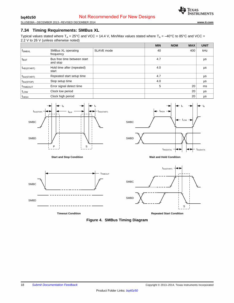
7.34 Timing Requirements: SMBus XLTypical values stated where TA = 25°C and VCC = 14.4 V, Min/Max values stated where TA = –40°C to 85°C and VCC =2.2 V to 26 V (unless otherwise noted)
MIN NOM MAX UNITfSMBXL SMBus XL operating SLAVE mode 40 400 kHz
frequencytBUF Bus free time between start 4.7 µs
and stoptHD(START) Hold time after (repeated) 4.0 µs
starttSU(START) Repeated start setup time 4.7 µstSU(STOP) Stop setup time 4.0 µstTIMEOUT Error signal detect time 5 20 mstLOW Clock low period 20 µstHIGH Clock high period 20 µs
Figure 4. SMBus Timing Diagram
18 Submit Documentation Feedback Copyright © 2013–2014, Texas Instruments Incorporated
Product Folder Links: bq40z50
Not Recommended For New Designs
16.6
16.7
16.8
16.9
±40 ±20 0 20 40 60 80 100 120
Hig
h-F
requ
ency
Osc
illat
or (
MH
z)
Temperature (C) C008
±25.8
±25.6
±25.4
±25.2
±25.0
±24.8
±24.6
±40 ±20 0 20 40 60 80 100 120
OC
D P
rote
ctio
n T
hres
hold
(m
V)
Temperature (C) C009
1.20
1.21
1.22
1.23
1.24
±40 ±20 0 20 40 60 80 100
Ref
eren
ce V
olta
ge (
V)
Temperature (C) C006
250
252
254
256
258
260
262
264
±40 ±20 0 20 40 60 80 100
Low
-Fre
quen
cy O
scill
ator
(kH
z)
Temperature (C) C007
±8.0
±6.0
±4.0
±2.0
0.0
2.0
4.0
6.0
8.0
±40 ±20 0 20 40 60 80 100 120
AD
C O
ffset
Err
or (
V/C
)
Temperature (C)
Max ADC Offset ErrorMin ADC Offset Error
C003
±0.15
±0.10
±0.05
0.00
0.05
0.10
0.15
±40 ±20 0 20 40 60 80 100 120
CC
Offs
et E
rror
(
V/C
)
Temperature (C)
Max CC Offset ErrorMin CC Offset Error
C001
bq40z50www.ti.com SLUSBS8A –DECEMBER 2013–REVISED DECEMBER 2014
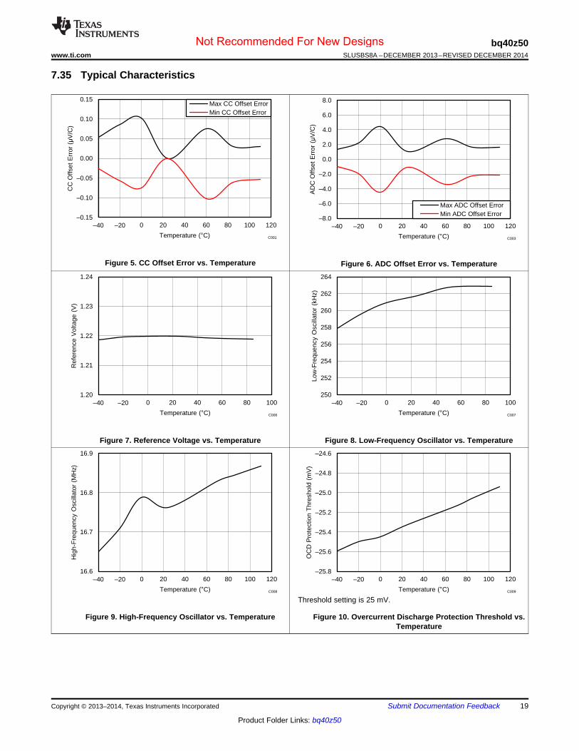
7.35 Typical Characteristics
Figure 5. CC Offset Error vs. Temperature Figure 6. ADC Offset Error vs. Temperature
Figure 7. Reference Voltage vs. Temperature Figure 8. Low-Frequency Oscillator vs. Temperature
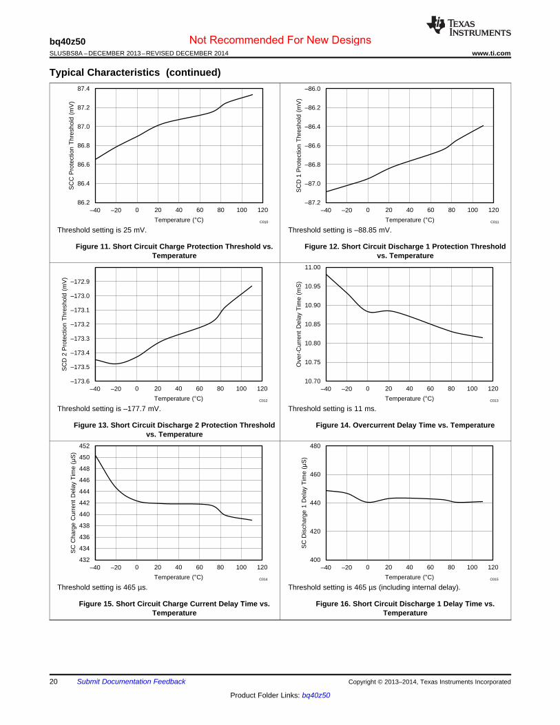
Threshold setting is 25 mV.
Figure 9. High-Frequency Oscillator vs. Temperature Figure 10. Overcurrent Discharge Protection Threshold vs.Temperature
Copyright © 2013–2014, Texas Instruments Incorporated Submit Documentation Feedback 19
Product Folder Links: bq40z50
Not Recommended For New Designs
432
434
436
438
440
442
444
446
448
450
452
±40 ±20 0 20 40 60 80 100 120
SC
Cha
rge
Cur
rent
Del
ay T
ime
(S
)
Temperature (C) C014
400
420
440
460
480
±40 ±20 0 20 40 60 80 100 120
SC
Dis
char
ge 1
Del
ay T
ime
(S
)
Temperature (C) C015
±173.6
±173.5
±173.4
±173.3
±173.2
±173.1
±173.0
±172.9
±40 ±20 0 20 40 60 80 100 120
SC
D 2
Pro
tect
ion
Thr
esho
ld (
mV
)
Temperature (C) C012
10.70
10.75
10.80
10.85
10.90
10.95
11.00
±40 ±20 0 20 40 60 80 100 120
Ove
r-C
urre
nt D
elay
Tim
e (m
S)
Temperature (C) C013
86.2
86.4
86.6
86.8
87.0
87.2
87.4
±40 ±20 0 20 40 60 80 100 120
SC
C P
rote
ctio
n T
hres
hold
(m
V)
Temperature (C) C010
±87.2
±87.0
±86.8
±86.6
±86.4
±86.2
±86.0
±40 ±20 0 20 40 60 80 100 120
SC
D 1
Pro
tect
ion
Thr
esho
ld (
mV
)
Temperature (C) C011
bq40z50SLUSBS8A –DECEMBER 2013–REVISED DECEMBER 2014 www.ti.com
Typical Characteristics (continued)
Threshold setting is 25 mV. Threshold setting is –88.85 mV.
Figure 11. Short Circuit Charge Protection Threshold vs. Figure 12. Short Circuit Discharge 1 Protection ThresholdTemperature vs. Temperature
Threshold setting is –177.7 mV. Threshold setting is 11 ms.
Figure 13. Short Circuit Discharge 2 Protection Threshold Figure 14. Overcurrent Delay Time vs. Temperaturevs. Temperature
Threshold setting is 465 µs. Threshold setting is 465 µs (including internal delay).
Figure 15. Short Circuit Charge Current Delay Time vs. Figure 16. Short Circuit Discharge 1 Delay Time vs.Temperature Temperature
20 Submit Documentation Feedback Copyright © 2013–2014, Texas Instruments Incorporated
Product Folder Links: bq40z50
Not Recommended For New Designs
4.2478
4.24785
4.2479
4.24795
4.248
4.24805
±40 ±20 0 20 40 60 80 100 120
Cel
l Vol
tage
(V
)
Temperature (C) C018
99.00
99.05
99.10
99.15
99.20
99.25
±40 ±20 0 20 40 60 80 100 120
Mea
sure
men
t C
urre
nt (
mA
)
Temperature (C) C019
2.498
2.49805
2.4981
2.49815
2.4982
2.49825
2.4983
2.49835
2.4984
±40 ±20 0 20 40 60 80 100 120
Cel
l Vol
tage
(V
)
Temperature (C) C016
3.498
3.49805
3.4981
3.49815
3.4982
3.49825
±40 ±20 0 20 40 60 80 100 120
Cel
l Vol
tage
(V
)
Temperature (C) C017
bq40z50www.ti.com SLUSBS8A –DECEMBER 2013–REVISED DECEMBER 2014
Typical Characteristics (continued)
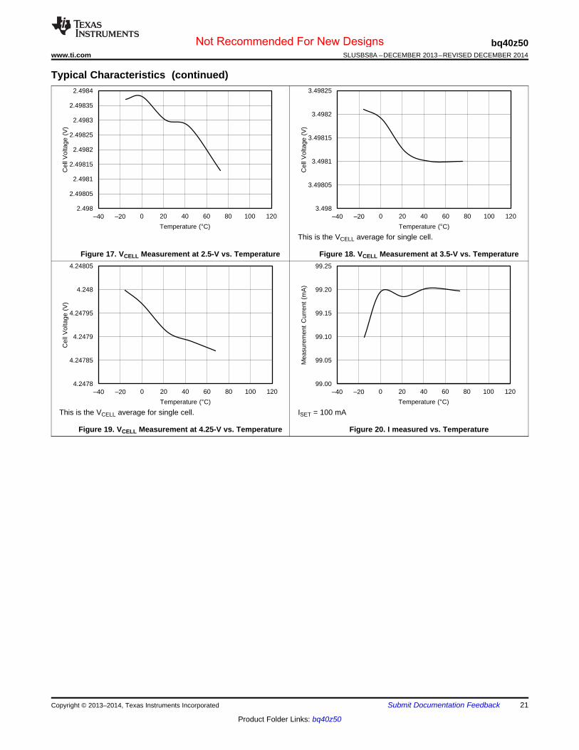
This is the VCELL average for single cell.
Figure 17. VCELL Measurement at 2.5-V vs. Temperature Figure 18. VCELL Measurement at 3.5-V vs. Temperature
This is the VCELL average for single cell. ISET = 100 mA
Figure 19. VCELL Measurement at 4.25-V vs. Temperature Figure 20. I measured vs. Temperature
Copyright © 2013–2014, Texas Instruments Incorporated Submit Documentation Feedback 21
Product Folder Links: bq40z50
Not Recommended For New Designs

DMAddr (16bit)
Cell
Balancing
Over
Current
Comparator
Short Circuit
Comparator
Power On
Reset
VoltageReference2
Watchdog
Timer
Zero Volt
ChargeControl
Wake
Comparator
InternalTemp
Sensor
Random
NumberGenerator
AFE ControlADC MUX
Cell Detach
Detection
High
Frequency
Oscillator
SBS COM
Engine
AFE COM
Engine
I/O &
Interrupt
Controller
Data Flash
EEPROM
ADC/CC
Digital Filter
Program
FlashEEPROM
bqBMP
CPU
Timers&
PWM
PMAddr(16bit)
PMInstr(8bit)
Cell, Stack,
Pack
Voltage
VoltageReference1
SMBC
SMBD
LEDCNTLA
LEDCNTLB
LEDCNTLC
/DISP
/PRES or /SHUTDN
BTP_INT
FUSE
PTCEN
SRP
PC
HG
DS
G
CH
G
VS
S
PA
CK
BA
T
VC
C
VC
4
VC
3
VC
2
VC
1
High Side
N-CH FET
Drive
P-CH
FET Drive
FUSE
Control
High
Voltage
I/O
LED Display
Drive I/O
PB
I
Power Mode
Control
SBS High
Voltage
Translation
Low
Frequency
Oscillator
ADC/CC
FRONTEND
1.8V LDO
Regulator
TS1
TS2
TS3
TS4
Low Voltage
I/O
PTC
Overtemp PTC
SRN
AFE COM
Engine
Data
SRAM
Data (8bit)
I /O
NTC Bias
bq40z50SLUSBS8A –DECEMBER 2013–REVISED DECEMBER 2014 www.ti.com
8 Detailed Description
8.1 OverviewThe bq40z50 device, incorporating patented Impedance Track™ technology, provides cell balancing whilecharging or at rest. This fully integrated, single-chip, pack-based solution provides a rich array of features for gasgauging, protection, and authentication for 1-series, 2-series, 3-series, and 4-series cell Li-Ion and Li-Polymerbattery packs, including a diagnostic lifetime data monitor and black box recorder.
8.2 Functional Block Diagram
22 Submit Documentation Feedback Copyright © 2013–2014, Texas Instruments Incorporated
Product Folder Links: bq40z50
Not Recommended For New Designs
bq40z50www.ti.com SLUSBS8A –DECEMBER 2013–REVISED DECEMBER 2014
8.3 Feature Description
8.3.1 Primary (1st Level) Safety FeaturesThe bq40z50 supports a wide range of battery and system protection features that can easily be configured. Seethe bq40z50 Technical Reference Manual (SLUUA43) for detailed descriptions of each protection function.
The primary safety features include:
• Cell Overvoltage Protection• Cell Undervoltage Protection• Cell Undervoltage Protection Compensated• Overcurrent in Charge Protection• Overcurrent in Discharge Protection• Overload in Discharge Protection• Short Circuit in Charge Protection• Short Circuit in Discharge Protection• Overtemperature in Charge Protection• Overtemperature in Discharge Protection• Undertemperature in Charge Protection• Undertemperature in Discharge Protection• Overtemperature FET protection• Precharge Timeout Protection• Host Watchdog Timeout Protection• Fast Charge Timeout Protection• Overcharge Protection• Overcharging Voltage Protection• Overcharging Current Protection• Over Precharge Current Protection
8.3.2 Secondary (2nd Level) Safety FeaturesThe secondary safety features of the bq40z50 can be used to indicate more serious faults via the FUSE pin. Thispin can be used to blow an in-line fuse to permanently disable the battery pack from charging or discharging.See the bq40z50 Technical Reference Manual (SLUUA43) for detailed descriptions of each protection function.
The secondary safety features provide protection against:• Safety Overvoltage Permanent Failure• Safety Undervoltage Permanent Failure• Safety Overtemperature Permanent Failure• Safety FET Overtemperature Permanent Failure• Qmax Imbalance Permanent Failure• Impedance Imbalance Permanent Failure• Capacity Degradation Permanent Failure• Cell Balancing Permanent Failure• Fuse Failure Permanent Failure• PTC Permanent Failure• Voltage Imbalance at Rest Permanent Failure• Voltage Imbalance Active Permanent Failure• Charge FET Permanent Failure• Discharge FET Permanent Failure• AFE Register Permanent Failure• AFE Communication Permanent Failure• Second Level Protector Permanent Failure
Copyright © 2013–2014, Texas Instruments Incorporated Submit Documentation Feedback 23
Product Folder Links: bq40z50
Not Recommended For New Designs
bq40z50SLUSBS8A –DECEMBER 2013–REVISED DECEMBER 2014 www.ti.com
Feature Description (continued)• Instruction Flash Checksum Permanent Failure• Open Cell Connection Permanent Failure• Data Flash Permanent Failure• Open Thermistor Permanent Failure
8.3.3 Charge Control FeaturesThe bq40z50 charge control features include:
• Supports JEITA temperature ranges. Reports charging voltage and charging current according to the activetemperature range
• Handles more complex charging profiles. Allows for splitting the standard temperature range into two sub-ranges and allows for varying the charging current according to the cell voltage
• Reports the appropriate charging current needed for constant current charging and the appropriate chargingvoltage needed for constant voltage charging to a smart charger using SMBus broadcasts
• Reduces the charge difference of the battery cells in fully charged state of the battery pack gradually using avoltage-based cell balancing algorithm during charging. A voltage threshold can be set up for cell balancing tobe active. This prevents fully charged cells from overcharging and causing excessive degradation and alsoincreases the usable pack energy by preventing premature charge termination.
• Supports pre-charging/zero-volt charging• Supports charge inhibit and charge suspend if battery pack temperature is out of temperature range• Reports charging fault and also indicates charge status via charge and discharge alarms
8.3.4 Gas GaugingThe bq40z50 uses the Impedance Track algorithm to measure and calculate the available capacity in batterycells. The bq40z50 accumulates a measure of charge and discharge currents and compensates the chargecurrent measurement for the temperature and state-of-charge of the battery. The bq40z50 estimates self-discharge of the battery and also adjusts the self-discharge estimation based on temperature. The device alsohas TURBO BOOST mode support, which enables the bq40z50 to provide the necessary data for the MCU todetermine what level of peak power consumption can be applied without causing a system reset or transientbattery voltage level spike to trigger termination flags. See the bq40z50 Technical Reference Manual (SLUUA43)for further details.
8.3.5 Configuration
8.3.5.1 Oscillator FunctionThe bq40z50 fully integrates the system oscillators and does not require any external components to support thisfeature.
8.3.5.2 System Present OperationThe bq40z50 checks the PRES pin periodically (1 s). If PRES input is pulled to ground by the external system,the bq40z50 detects this as system present.
8.3.5.3 Emergency ShutdownFor battery maintenance, the emergency shutdown feature enables a push button action connecting theSHUTDN pin to shutdown an embedded battery pack system before removing the battery. A high-to-lowtransition of the SHUTDN pin signals the bq40z50 to turn off both CHG and DSG FETs, disconnecting the powerfrom the system to safely remove the battery pack. The CHG and DSG FETs can be turned on again by anotherhigh-to-low transition detected by the SHUTDN pin or when a data flash configurable timeout is reached.
8.3.5.4 1-Series, 2-Series, 3-Series, or 4-Series Cell ConfigurationIn a 1-series cell configuration, VC4 is shorted to VC, VC2 and VC1. In a 2-series cell configuration, VC4 isshorted to VC3 and VC2. In a 3-series cell configuration, VC4 is shorted to VC3.
24 Submit Documentation Feedback Copyright © 2013–2014, Texas Instruments Incorporated
Product Folder Links: bq40z50
Not Recommended For New Designs
bq40z50www.ti.com SLUSBS8A –DECEMBER 2013–REVISED DECEMBER 2014
Feature Description (continued)8.3.5.5 Cell BalancingThe device supports cell balancing by bypassing the current of each cell during charging or at rest. If the device'sinternal bypass is used, up to 10 mA can be bypassed and multiple cells can be bypassed at the same time.Higher cell balance current can be achieved by using an external cell balancing circuit. In external cell balancingmode, only one cell at a time can be balanced.
The cell balancing algorithm determines the amount of charge needed to be bypassed to balance the capacity ofall cells.
8.3.6 Battery Parameter Measurements
8.3.6.1 Charge and Discharge CountingThe bq40z50 uses an integrating delta-sigma analog-to-digital converter (ADC) for current measurement, and asecond delta-sigma ADC for individual cell and battery voltage and temperature measurement.
The integrating delta-sigma ADC measures the charge/discharge flow of the battery by measuring the voltagedrop across a small-value sense resistor between the SRP and SRN terminals. The integrating ADC measuresbipolar signals from –0.1 V to 0.1 V. The bq40z50 detects charge activity when VSR = V(SRP) – V(SRN) is positive,and discharge activity when VSR = V(SRP) – V(SRN) is negative. The bq40z50 continuously integrates the signalover time, using an internal counter. The fundamental rate of the counter is 0.26 nVh.
8.3.7 Battery Trip Point (BTP)Required for WIN8 OS, the battery trip point (BTP) feature indicates when the RSOC of a battery pack hasdepleted to a certain value set in a DF register. This feature allows a host to program two capacity-basedthresholds that govern the triggering of a BTP interrupt on the BTP_INT pin and the setting or clearing of theOperationStatus[BTP_INT] on the basis of RemainingCapacity().
An internal weak pull-up is applied when the BTP feature is active. Depending on the system design, an externalpull-up may be required to put on the BTP_INT pin. See Electrical Characteristics: PRES, BTP_INT, DISP fordetails.
8.3.8 Lifetime Data Logging FeaturesThe bq40z50 offers lifetime data logging for several critical battery parameters. The following parameters areupdated every 10 hours if a difference is detected between values in RAM and data flash:• Maximum and Minimum Cell Voltages• Maximum Delta Cell Voltage• Maximum Charge Current• Maximum Discharge Current• Maximum Average Discharge Current• Maximum Average Discharge Power• Maximum and Minimum Cell Temperature• Maximum Delta Cell Temperature• Maximum and Minimum Internal Sensor Temperature• Maximum FET Temperature• Number of Safety Events Occurrences and the Last Cycle of the Occurrence• Number of Valid Charge Termination and the Last Cycle of the Valid Charge Termination• Number of Qmax and Ra Updates and the Last Cycle of the Qmax and Ra Updates• Number of Shutdown Events• Cell Balancing Time for Each Cell
(This data is updated every 2 hours if a difference is detected.)• Total FW Runtime and Time Spent in Each Temperature Range
(This data is updated every 2 hours if a difference is detected.)
Copyright © 2013–2014, Texas Instruments Incorporated Submit Documentation Feedback 25
Product Folder Links: bq40z50
Not Recommended For New Designs
bq40z50SLUSBS8A –DECEMBER 2013–REVISED DECEMBER 2014 www.ti.com
Feature Description (continued)8.3.9 AuthenticationThe bq40z50 supports authentication by the host using SHA-1.
8.3.10 LED DisplayThe bq40z50 can drive a 3-, 4-, or 5- segment LED display for remaining capacity indication and/or a permanentfail (PF) error code indication.
8.3.11 VoltageThe bq40z50 updates the individual series cell voltages at 0.25-second intervals. The internal ADC of thebq40z50 measures the voltage, and scales and calibrates it appropriately. This data is also used to calculate theimpedance of the cell for the Impedance Track gas gauging.
8.3.12 CurrentThe bq40z50 uses the SRP and SRN inputs to measure and calculate the battery charge and discharge currentusing a 1-mΩ to 3-mΩ typ. sense resistor.
8.3.13 TemperatureThe bq40z50 has an internal temperature sensor and inputs for four external temperature sensors. All fivetemperature sensor options can be individually enabled and configured for cell or FET temperature usage. Twoconfigurable thermistor models are provided to allow the monitoring of cell temperature in addition to FETtemperature, which use a different thermistor profile.
8.3.14 CommunicationsThe bq40z50 uses SMBus v1.1 with MASTER mode and packet error checking (PEC) options per the SBSspecification.
8.3.14.1 SMBus On and Off StateThe bq40z50 detects an SMBus off state when SMBC and SMBD are low for two or more seconds. Clearing thisstate requires that either SMBC or SMBD transition high. The communication bus will resume activity within1 ms.
8.3.14.2 SBS CommandsSee the bq40z50 Technical Reference Manual (SLUUA43) for further details.
8.4 Device Functional ModesThe bq40z50 supports three power modes to reduce power consumption:• In NORMAL mode, the bq40z50 performs measurements, calculations, protection decisions, and data
updates in 250-ms intervals. Between these intervals, the bq40z50 is in a reduced power stage.• In SLEEP mode, the bq40z50 performs measurements, calculations, protection decisions, and data updates
in adjustable time intervals. Between these intervals, the bq40z50 is in a reduced power stage. The bq40z50has a wake function that enables exit from SLEEP mode when current flow or failure is detected.
• In SHUTDOWN mode, the bq40z50 is completely disabled.
26 Submit Documentation Feedback Copyright © 2013–2014, Texas Instruments Incorporated
Product Folder Links: bq40z50
Not Recommended For New Designs
bq40z50www.ti.com SLUSBS8A –DECEMBER 2013–REVISED DECEMBER 2014
9 Applications and Implementation
NOTEInformation in the following applications sections is not part of the TI componentspecification, and TI does not warrant its accuracy or completeness. TI’s customers areresponsible for determining suitability of components for their purposes. Customers shouldvalidate and test their design implementation to confirm system functionality.
9.1 Application InformationThe bq40z50 is a gas gauge with primary protection support, and that can be used with a 1-series to 4-series Li-Ion/Li Polymer battery pack. To implement and design a comprehensive set of parameters for a specific batterypack, users need the Battery Management Studio (bqSTUDIO) graphical user-interface tool installed on a PCduring development. The firmware installed on the bqSTUDIO tool has default values for this product, which aresummarized in the bq40z50 Technical Reference Manual (SLUUA43). Using the bqSTUDIO tool, these defaultvalues can be changed to cater to specific application requirements during development once the systemparameters, such as fault trigger thresholds for protection, enable/disable of certain features for operation,configuration of cells, chemistry that best matches the cell used, and more are known. This data is referred to asthe "golden image."
Copyright © 2013–2014, Texas Instruments Incorporated Submit Documentation Feedback 27
Product Folder Links: bq40z50
Not Recommended For New Designs
2P
1P
1N
4P
3P
Sys
Pre
s
PA
CK
-
PA
CK
+
SR
PS
RN
BA
T
CH
G
DS
G
FU
SE
PIN
FU
SE
1
1
ICgro
un
d s
ho
uld
be
co
nne
cte
dto
the
1N
ce
llta
b.
Pla
ce
RT1
clo
se
toQ
2and
Q3
.2
SM
BC
SM
BD
2
Wa
ke
For
Th
um
bu
s-S
MB
LE
D3
LE
D5
LE
D2
LE
D4
LE
D1
0.1
uF
C8
0.1
uF
C10
12
GND SIDE
12
GND SIDE
12
GND SIDE
12
GND SIDE
1 2 3 4J2
10
0
R25
10
0
R27
1K
R29
20
0
R24
20
0
R26
20
0
R28
10K
RT
2
10
0
R30
10
0
R31
DN
P
C19
DN
P
C20
0.1
uF
C18
0.0
01
R19
0.1
uF
C12
1 2 3
J3
1 2J4
123
J5
12
J1
10
0
R20
10
0
R21
10
0
R22
10
0
R23
0.1
uF
C14
0.1
uF
C15
0.1
uF
C16
0.1
uF
C17
2.2
uF
C13
BA
T5
4H
T1
D1
0.1
uF
C4
0.1
uF
C5
0.1
uF
C9
0.1
uF
C1
11
K
R18
0.1
uF
C6
0.1
uF
C7
Si1
406D
H
12
3
45
6
Q5
51K
R6
0.1
uF
C3
12
3
SF
Dxxxx
F1
5.1
K
R16
5.1
K
R17
5.1
K
R7
R8
10
0
R9
5.1
K
R10
10K
R12
10
M
R2
10M
R3
10
M
R5
0.1
uF
C1
0.1
uF
C2
Si7
116D
N
123
4
5
Q2
Si7
116D
N
123
4
5
Q3
30
0
R1
2N
70
02
K1
23
Q4
10K
R4
10K
RT
3
10K
RT
4
10K
RT
5
11
11
11
11
11
11
11
11
MM3ZxxVyC
D2
MM3ZxxVyC
D3
MM3ZxxVyC
D4
FD
N358
P
1
32
Q1
BQ
29
47xyD
SG
VD
D1
V4
2
V3
3
V2
4V
15
VS
S6
CD
7
OU
T8
EP9
U2
PB
I1
VC
42
VC
33
VC
24
VC
15
SR
N6
NC
7
SR
P8
VSS9
TS110
TS211
TS312
TS413
NC14
BTP_INT15
PRESorSHUTDN16
DIS
P17
SM
BD
18
SM
BC
19
LE
DC
NT
LA
20
LE
DC
NT
LB
21
LE
DC
NT
LC
22
PT
C23
PT
CE
N24
FUSE25
VCC26
PACK27
DSG28
NC29
PCHG30
CHG31
BAT32
PWPD33
10K
R32
12345
67
J6
CH
GN
D
CHGND
BA
T
4P
SMBD
SMBC
PA
CK
+
GN
D
BA
T
GN
D
BA
T
CH
GN
D
CH
GN
D
CH
GN
D
GN
DG
ND
GN
D
GN
D
GN
D
CH
GN
D
GN
D
GN
D
AG
ND
AG
ND
4P
PA
CK
+
4P
PA
CK
+
CH
GN
D
I2C
_V
OU
T
SM
BD
SM
BC
SMBC
SMBD
GN
D
AA
'B
B'
S1
GN
D
AA
'B
B'
S3
AA
'B
B'
S2
GN
D
DN
P
C21
11
D5
D6
D7
D9
D8
NT
1N
et-T
ie
PA
CK
-
PA
CK
+
LE
DD
ISP
LA
Y
SH
UTD
OW
N
11T
P1
2
12
J7
10K
RT
1
GN
D
11
11
TP
3
1K
R13
1K
R14
1K
R15
10
0
R1
1
VS
S
SM
BD
SM
BC
GN
D
3R
ep
lace
D1
an
dR
9w
ith a
10
oh
mre
sis
tor
for s
ing
lece
lla
pp
lica
tion
s
3
3
5.1
K
bq40z50SLUSBS8A –DECEMBER 2013–REVISED DECEMBER 2014 www.ti.com
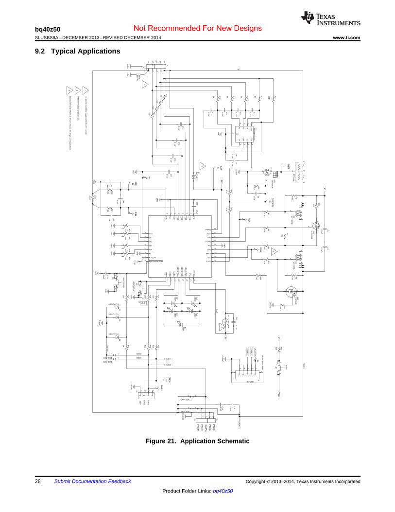
9.2 Typical Applications
Figure 21. Application Schematic
28 Submit Documentation Feedback Copyright © 2013–2014, Texas Instruments Incorporated
Product Folder Links: bq40z50
Not Recommended For New Designs
bq40z50www.ti.com SLUSBS8A –DECEMBER 2013–REVISED DECEMBER 2014
Typical Applications (continued)9.2.1 Design RequirementsTable 1 shows the default settings for the main parameters. Use the bqSTUDIO tool to update the settings tomeet the specific application or battery pack configuration requirements.
The device should be calibrated before any gauging test. Follow the bqSTUDIO Calibration page to calibrate thedevice, and use the bqSTUDIO Chemistry page to update the match chemistry profile to the device.
Table 1. Design ParametersDESIGN PARAMETER EXAMPLE
Cell Configuration 3s1p (3-series with 1 Parallel) (1)
Design Capacity 4400 mAhDevice Chemistry 1210 (LiCoO2/graphitized carbon)
Cell Overvoltage at Standard Temperature 4300 mVCell Undervoltage 2500 mVShutdown Voltage 2300 mV
Overcurrent in CHARGE Mode 6000 mAOvercurrent in DISCHARGE Mode –6000 mA
Short Circuit in CHARGE Mode 0.1 V/Rsense across SRP, SRNShort Circuit in DISCHARGE Mode 0.1 V/Rsense across SRP, SRN
Safety Overvoltage 4500 mVCell Balancing Disabled
Internal and External Temperature Sensor External Temperature Sensor is used.Undertemperature Charging 0°C
Undertemperature Discharging 0°CBROADCAST Mode Disabled
Battery Trip Point (BTP) with active high interrupt Disabled
(1) When using the device the first time, if the a 1-s or 2-s battery pack is used, then a charger or power supply should be connected to thePACK+ terminal to prevent device shutdown. Then update the cell configuration (see the bq40z50 Technical Reference Manual(SLUUA43) for details) before removing the charger connection.
9.2.2 Detailed Design Procedure
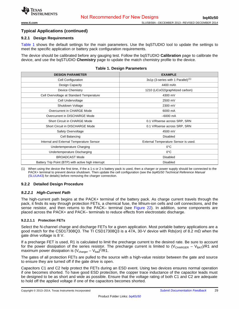
9.2.2.1 High-Current PathThe high-current path begins at the PACK+ terminal of the battery pack. As charge current travels through thepack, it finds its way through protection FETs, a chemical fuse, the lithium-ion cells and cell connections, and thesense resistor, and then returns to the PACK– terminal (see Figure 22). In addition, some components areplaced across the PACK+ and PACK– terminals to reduce effects from electrostatic discharge.
9.2.2.1.1 Protection FETs
Select the N-channel charge and discharge FETs for a given application. Most portable battery applications are agood match for the CSD17308Q3. The TI CSD17308Q3 is a 47A, 30-V device with Rds(on) of 8.2 mΩ when thegate drive voltage is 8 V.
If a precharge FET is used, R1 is calculated to limit the precharge current to the desired rate. Be sure to accountfor the power dissipation of the series resistor. The precharge current is limited to (VCHARGER – VBAT)/R1 andmaximum power dissipation is (Vcharger – Vbat)2/R1.
The gates of all protection FETs are pulled to the source with a high-value resistor between the gate and sourceto ensure they are turned off if the gate drive is open.
Capacitors C1 and C2 help protect the FETs during an ESD event. Using two devices ensures normal operationif one becomes shorted. To have good ESD protection, the copper trace inductance of the capacitor leads mustbe designed to be as short and wide as possible. Ensure that the voltage rating of both C1 and C2 are adequateto hold off the applied voltage if one of the capacitors becomes shorted.
Copyright © 2013–2014, Texas Instruments Incorporated Submit Documentation Feedback 29
Product Folder Links: bq40z50
Not Recommended For New Designs
bq40z50SLUSBS8A –DECEMBER 2013–REVISED DECEMBER 2014 www.ti.com
Figure 22. bq40z50 Protection FETs
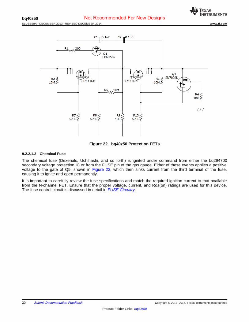
9.2.2.1.2 Chemical Fuse
The chemical fuse (Dexerials, Uchihashi, and so forth) is ignited under command from either the bq294700secondary voltage protection IC or from the FUSE pin of the gas gauge. Either of these events applies a positivevoltage to the gate of Q5, shown in Figure 23, which then sinks current from the third terminal of the fuse,causing it to ignite and open permanently.
It is important to carefully review the fuse specifications and match the required ignition current to that availablefrom the N-channel FET. Ensure that the proper voltage, current, and Rds(on) ratings are used for this device.The fuse control circuit is discussed in detail in FUSE Circuitry.
30 Submit Documentation Feedback Copyright © 2013–2014, Texas Instruments Incorporated
Product Folder Links: bq40z50
Not Recommended For New Designs
bq40z50www.ti.com SLUSBS8A –DECEMBER 2013–REVISED DECEMBER 2014
Figure 23. FUSE Circuit
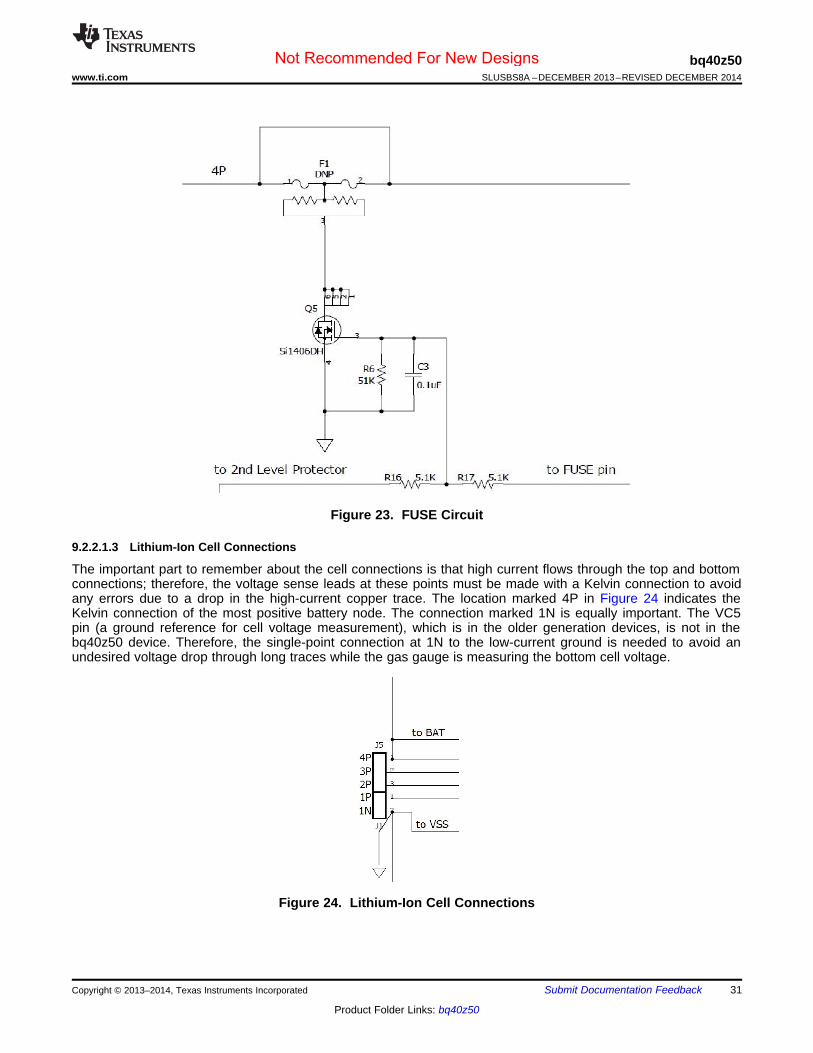
9.2.2.1.3 Lithium-Ion Cell Connections
The important part to remember about the cell connections is that high current flows through the top and bottomconnections; therefore, the voltage sense leads at these points must be made with a Kelvin connection to avoidany errors due to a drop in the high-current copper trace. The location marked 4P in Figure 24 indicates theKelvin connection of the most positive battery node. The connection marked 1N is equally important. The VC5pin (a ground reference for cell voltage measurement), which is in the older generation devices, is not in thebq40z50 device. Therefore, the single-point connection at 1N to the low-current ground is needed to avoid anundesired voltage drop through long traces while the gas gauge is measuring the bottom cell voltage.
Figure 24. Lithium-Ion Cell Connections
Copyright © 2013–2014, Texas Instruments Incorporated Submit Documentation Feedback 31
Product Folder Links: bq40z50
Not Recommended For New Designs
bq40z50SLUSBS8A –DECEMBER 2013–REVISED DECEMBER 2014 www.ti.com
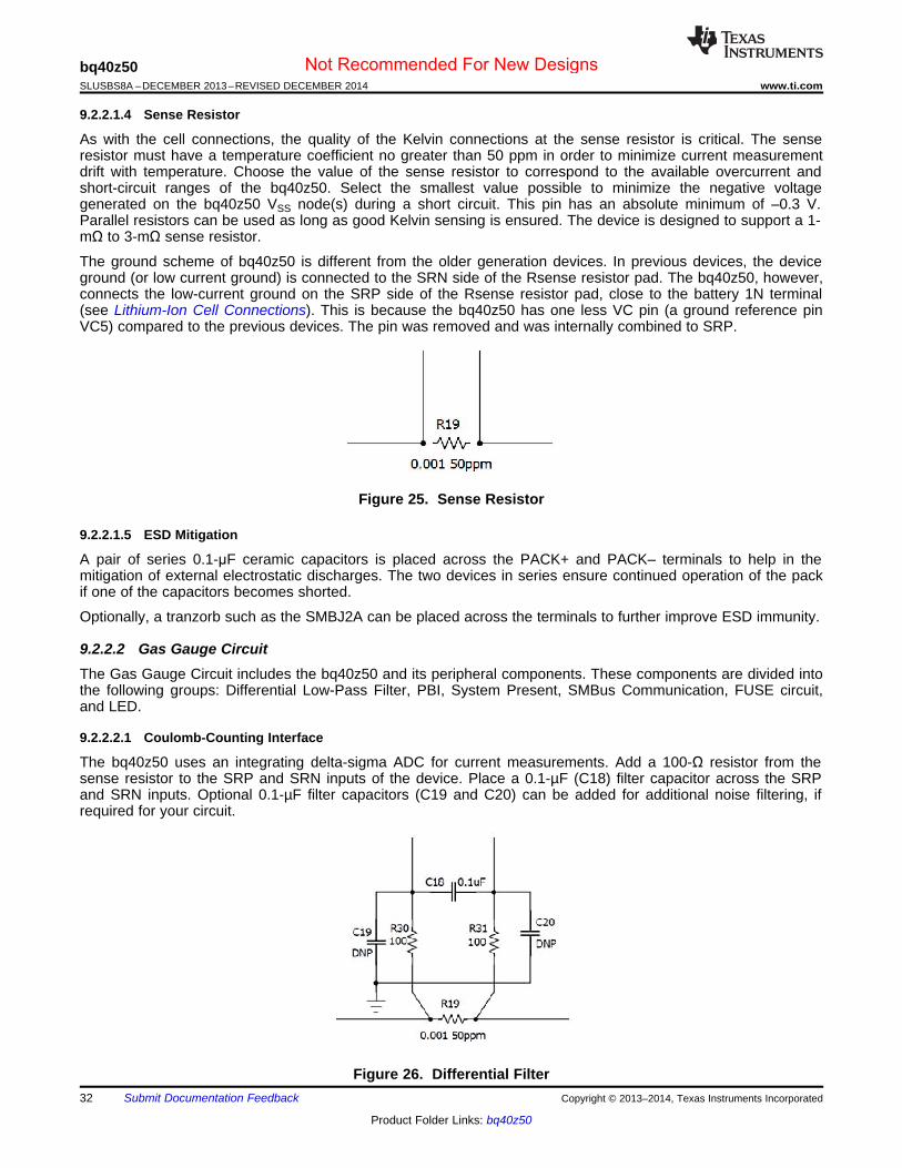
9.2.2.1.4 Sense Resistor
As with the cell connections, the quality of the Kelvin connections at the sense resistor is critical. The senseresistor must have a temperature coefficient no greater than 50 ppm in order to minimize current measurementdrift with temperature. Choose the value of the sense resistor to correspond to the available overcurrent andshort-circuit ranges of the bq40z50. Select the smallest value possible to minimize the negative voltagegenerated on the bq40z50 VSS node(s) during a short circuit. This pin has an absolute minimum of –0.3 V.Parallel resistors can be used as long as good Kelvin sensing is ensured. The device is designed to support a 1-mΩ to 3-mΩ sense resistor.
The ground scheme of bq40z50 is different from the older generation devices. In previous devices, the deviceground (or low current ground) is connected to the SRN side of the Rsense resistor pad. The bq40z50, however,connects the low-current ground on the SRP side of the Rsense resistor pad, close to the battery 1N terminal(see Lithium-Ion Cell Connections). This is because the bq40z50 has one less VC pin (a ground reference pinVC5) compared to the previous devices. The pin was removed and was internally combined to SRP.
Figure 25. Sense Resistor
9.2.2.1.5 ESD Mitigation
A pair of series 0.1-μF ceramic capacitors is placed across the PACK+ and PACK– terminals to help in themitigation of external electrostatic discharges. The two devices in series ensure continued operation of the packif one of the capacitors becomes shorted.
Optionally, a tranzorb such as the SMBJ2A can be placed across the terminals to further improve ESD immunity.
9.2.2.2 Gas Gauge CircuitThe Gas Gauge Circuit includes the bq40z50 and its peripheral components. These components are divided intothe following groups: Differential Low-Pass Filter, PBI, System Present, SMBus Communication, FUSE circuit,and LED.
9.2.2.2.1 Coulomb-Counting Interface
The bq40z50 uses an integrating delta-sigma ADC for current measurements. Add a 100-Ω resistor from thesense resistor to the SRP and SRN inputs of the device. Place a 0.1-µF (C18) filter capacitor across the SRPand SRN inputs. Optional 0.1-µF filter capacitors (C19 and C20) can be added for additional noise filtering, ifrequired for your circuit.
Figure 26. Differential Filter32 Submit Documentation Feedback Copyright © 2013–2014, Texas Instruments Incorporated
Product Folder Links: bq40z50
Not Recommended For New Designs
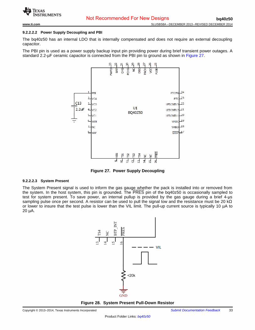
bq40z50www.ti.com SLUSBS8A –DECEMBER 2013–REVISED DECEMBER 2014
9.2.2.2.2 Power Supply Decoupling and PBI
The bq40z50 has an internal LDO that is internally compensated and does not require an external decouplingcapacitor.
The PBI pin is used as a power supply backup input pin providing power during brief transient power outages. Astandard 2.2-µF ceramic capacitor is connected from the PBI pin to ground as shown in Figure 27.
Figure 27. Power Supply Decoupling
9.2.2.2.3 System Present
The System Present signal is used to inform the gas gauge whether the pack is installed into or removed fromthe system. In the host system, this pin is grounded. The PRES pin of the bq40z50 is occasionally sampled totest for system present. To save power, an internal pullup is provided by the gas gauge during a brief 4-μssampling pulse once per second. A resistor can be used to pull the signal low and the resistance must be 20 kΩor lower to insure that the test pulse is lower than the VIL limit. The pull-up current source is typically 10 µA to20 µA.
Figure 28. System Present Pull-Down ResistorCopyright © 2013–2014, Texas Instruments Incorporated Submit Documentation Feedback 33
Product Folder Links: bq40z50
Not Recommended For New Designs
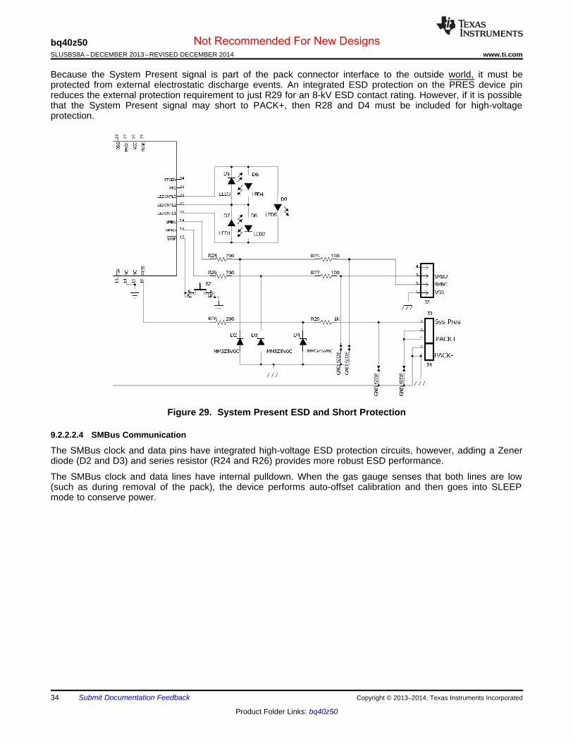
bq40z50SLUSBS8A –DECEMBER 2013–REVISED DECEMBER 2014 www.ti.com
Because the System Present signal is part of the pack connector interface to the outside world, it must beprotected from external electrostatic discharge events. An integrated ESD protection on the PRES device pinreduces the external protection requirement to just R29 for an 8-kV ESD contact rating. However, if it is possiblethat the System Present signal may short to PACK+, then R28 and D4 must be included for high-voltageprotection.
Figure 29. System Present ESD and Short Protection
9.2.2.2.4 SMBus Communication
The SMBus clock and data pins have integrated high-voltage ESD protection circuits, however, adding a Zenerdiode (D2 and D3) and series resistor (R24 and R26) provides more robust ESD performance.
The SMBus clock and data lines have internal pulldown. When the gas gauge senses that both lines are low(such as during removal of the pack), the device performs auto-offset calibration and then goes into SLEEPmode to conserve power.
34 Submit Documentation Feedback Copyright © 2013–2014, Texas Instruments Incorporated
Product Folder Links: bq40z50
Not Recommended For New Designs
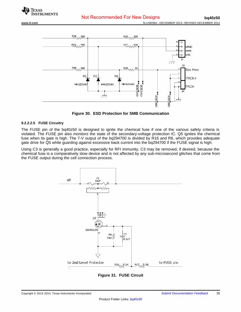
bq40z50www.ti.com SLUSBS8A –DECEMBER 2013–REVISED DECEMBER 2014
Figure 30. ESD Protection for SMB Communication
9.2.2.2.5 FUSE Circuitry
The FUSE pin of the bq40z50 is designed to ignite the chemical fuse if one of the various safety criteria isviolated. The FUSE pin also monitors the state of the secondary-voltage protection IC. Q5 ignites the chemicalfuse when its gate is high. The 7-V output of the bq294700 is divided by R16 and R6, which provides adequategate drive for Q5 while guarding against excessive back current into the bq294700 if the FUSE signal is high.
Using C3 is generally a good practice, especially for RFI immunity. C3 may be removed, if desired, because thechemical fuse is a comparatively slow device and is not affected by any sub-microsecond glitches that come fromthe FUSE output during the cell connection process.
Figure 31. FUSE Circuit
Copyright © 2013–2014, Texas Instruments Incorporated Submit Documentation Feedback 35
Product Folder Links: bq40z50
Not Recommended For New Designs
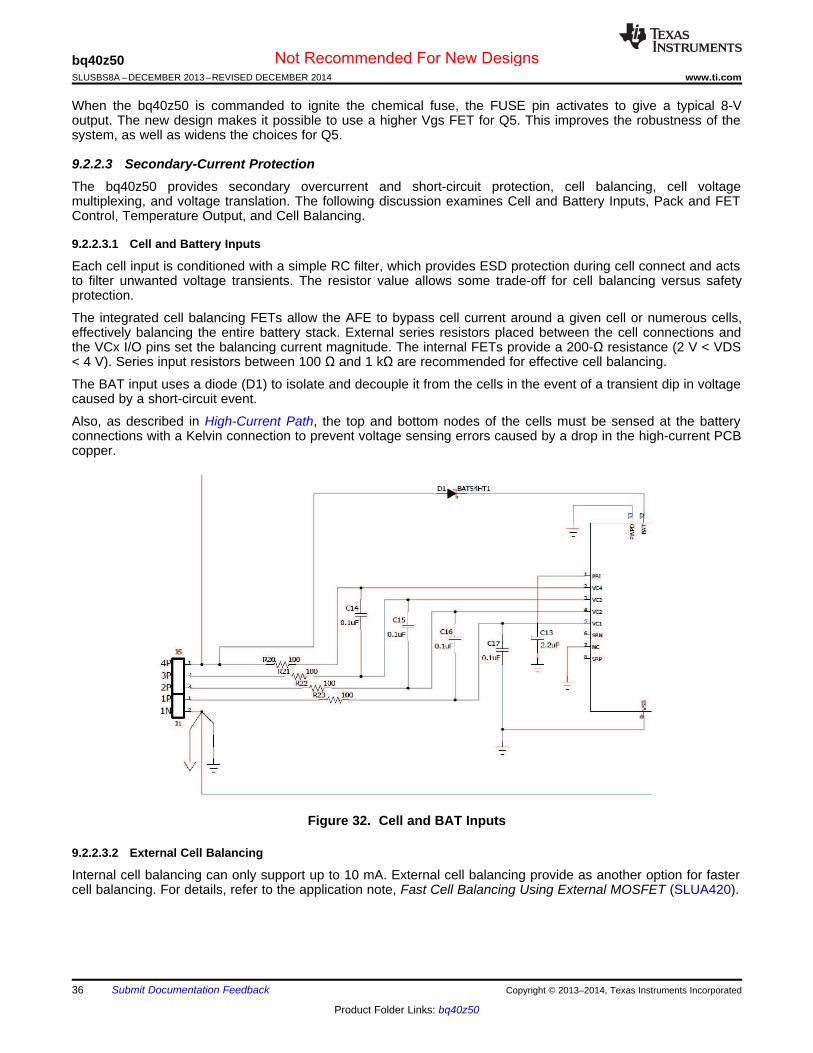
bq40z50SLUSBS8A –DECEMBER 2013–REVISED DECEMBER 2014 www.ti.com
When the bq40z50 is commanded to ignite the chemical fuse, the FUSE pin activates to give a typical 8-Voutput. The new design makes it possible to use a higher Vgs FET for Q5. This improves the robustness of thesystem, as well as widens the choices for Q5.
9.2.2.3 Secondary-Current ProtectionThe bq40z50 provides secondary overcurrent and short-circuit protection, cell balancing, cell voltagemultiplexing, and voltage translation. The following discussion examines Cell and Battery Inputs, Pack and FETControl, Temperature Output, and Cell Balancing.
9.2.2.3.1 Cell and Battery Inputs
Each cell input is conditioned with a simple RC filter, which provides ESD protection during cell connect and actsto filter unwanted voltage transients. The resistor value allows some trade-off for cell balancing versus safetyprotection.
The integrated cell balancing FETs allow the AFE to bypass cell current around a given cell or numerous cells,effectively balancing the entire battery stack. External series resistors placed between the cell connections andthe VCx I/O pins set the balancing current magnitude. The internal FETs provide a 200-Ω resistance (2 V < VDS< 4 V). Series input resistors between 100 Ω and 1 kΩ are recommended for effective cell balancing.
The BAT input uses a diode (D1) to isolate and decouple it from the cells in the event of a transient dip in voltagecaused by a short-circuit event.
Also, as described in High-Current Path, the top and bottom nodes of the cells must be sensed at the batteryconnections with a Kelvin connection to prevent voltage sensing errors caused by a drop in the high-current PCBcopper.
Figure 32. Cell and BAT Inputs
9.2.2.3.2 External Cell Balancing
Internal cell balancing can only support up to 10 mA. External cell balancing provide as another option for fastercell balancing. For details, refer to the application note, Fast Cell Balancing Using External MOSFET (SLUA420).
36 Submit Documentation Feedback Copyright © 2013–2014, Texas Instruments Incorporated
Product Folder Links: bq40z50
Not Recommended For New Designs
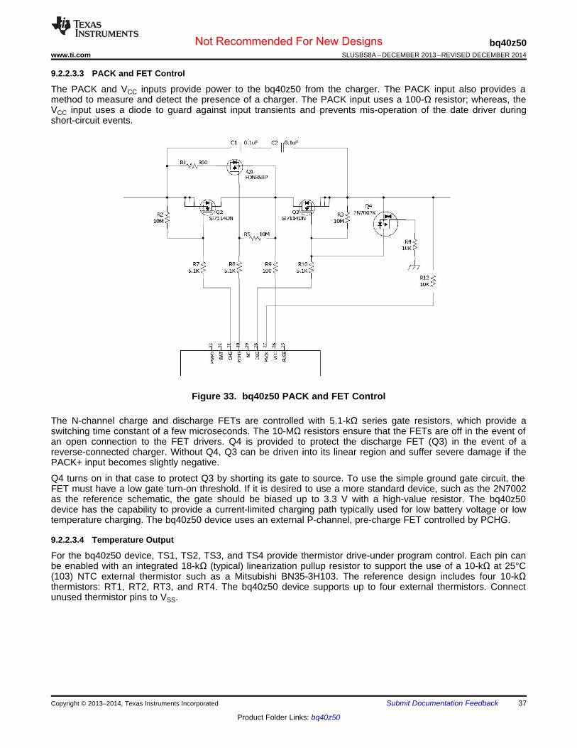
bq40z50www.ti.com SLUSBS8A –DECEMBER 2013–REVISED DECEMBER 2014
9.2.2.3.3 PACK and FET Control
The PACK and VCC inputs provide power to the bq40z50 from the charger. The PACK input also provides amethod to measure and detect the presence of a charger. The PACK input uses a 100-Ω resistor; whereas, theVCC input uses a diode to guard against input transients and prevents mis-operation of the date driver duringshort-circuit events.
Figure 33. bq40z50 PACK and FET Control
The N-channel charge and discharge FETs are controlled with 5.1-kΩ series gate resistors, which provide aswitching time constant of a few microseconds. The 10-MΩ resistors ensure that the FETs are off in the event ofan open connection to the FET drivers. Q4 is provided to protect the discharge FET (Q3) in the event of areverse-connected charger. Without Q4, Q3 can be driven into its linear region and suffer severe damage if thePACK+ input becomes slightly negative.
Q4 turns on in that case to protect Q3 by shorting its gate to source. To use the simple ground gate circuit, theFET must have a low gate turn-on threshold. If it is desired to use a more standard device, such as the 2N7002as the reference schematic, the gate should be biased up to 3.3 V with a high-value resistor. The bq40z50device has the capability to provide a current-limited charging path typically used for low battery voltage or lowtemperature charging. The bq40z50 device uses an external P-channel, pre-charge FET controlled by PCHG.
9.2.2.3.4 Temperature Output
For the bq40z50 device, TS1, TS2, TS3, and TS4 provide thermistor drive-under program control. Each pin canbe enabled with an integrated 18-kΩ (typical) linearization pullup resistor to support the use of a 10-kΩ at 25°C(103) NTC external thermistor such as a Mitsubishi BN35-3H103. The reference design includes four 10-kΩthermistors: RT1, RT2, RT3, and RT4. The bq40z50 device supports up to four external thermistors. Connectunused thermistor pins to VSS.
Copyright © 2013–2014, Texas Instruments Incorporated Submit Documentation Feedback 37
Product Folder Links: bq40z50
Not Recommended For New Designs
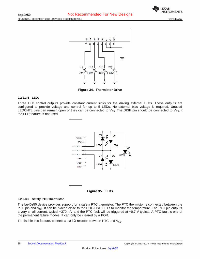
bq40z50SLUSBS8A –DECEMBER 2013–REVISED DECEMBER 2014 www.ti.com
Figure 34. Thermistor Drive
9.2.2.3.5 LEDs
Three LED control outputs provide constant current sinks for the driving external LEDs. These outputs areconfigured to provide voltage and control for up to 5 LEDs. No external bias voltage is required. UnusedLEDCNTL pins can remain open or they can be connected to VSS. The DISP pin should be connected to VSS, ifthe LED feature is not used.
Figure 35. LEDs
9.2.2.3.6 Safety PTC Thermistor
The bq40z50 device provides support for a safety PTC thermistor. The PTC thermistor is connected between thePTC pin and VSS. It can be placed close to the CHG/DSG FETs to monitor the temperature. The PTC pin outputsa very small current, typical ~370 nA, and the PTC fault will be triggered at ~0.7 V typical. A PTC fault is one ofthe permanent failure modes. It can only be cleared by a POR.
To disable this feature, connect a 10-kΩ resistor between PTC and VSS.
38 Submit Documentation Feedback Copyright © 2013–2014, Texas Instruments Incorporated
Product Folder Links: bq40z50
Not Recommended For New Designs
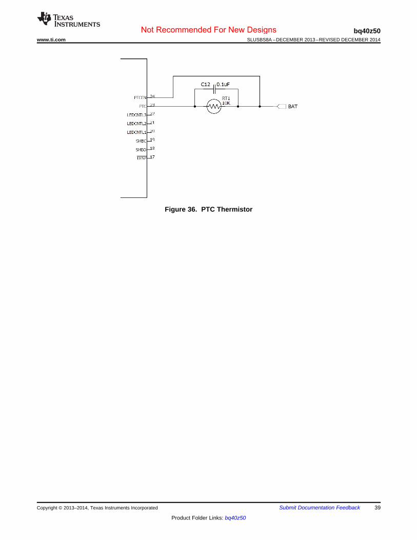
bq40z50www.ti.com SLUSBS8A –DECEMBER 2013–REVISED DECEMBER 2014
Figure 36. PTC Thermistor
Copyright © 2013–2014, Texas Instruments Incorporated Submit Documentation Feedback 39
Product Folder Links: bq40z50
Not Recommended For New Designs
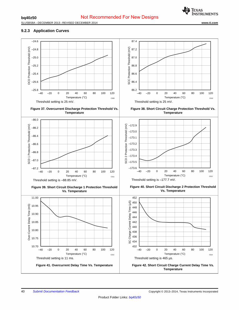
10.70
10.75
10.80
10.85
10.90
10.95
11.00
±40 ±20 0 20 40 60 80 100 120
Ove
r-C
urre
nt D
elay
Tim
e (m
S)
Temperature (C) C013
432
434
436
438
440
442
444
446
448
450
452
±40 ±20 0 20 40 60 80 100 120
SC
Cha
rge
Cur
rent
Del
ay T
ime
(S
)
Temperature (C) C014
±87.2
±87.0
±86.8
±86.6
±86.4
±86.2
±86.0
±40 ±20 0 20 40 60 80 100 120
SC
D 1
Pro
tect
ion
Thr
esho
ld (
mV
)
Temperature (C) C011
±173.6
±173.5
±173.4
±173.3
±173.2
±173.1
±173.0
±172.9
±40 ±20 0 20 40 60 80 100 120
SC
D 2
Pro
tect
ion
Thr
esho
ld (
mV
)
Temperature (C) C012
±25.8
±25.6
±25.4
±25.2
±25.0
±24.8
±24.6
±40 ±20 0 20 40 60 80 100 120
OC
D P
rote
ctio
n T
hres
hold
(m
V)
Temperature (C) C009
86.2
86.4
86.6
86.8
87.0
87.2
87.4
±40 ±20 0 20 40 60 80 100 120
SC
C P
rote
ctio
n T
hres
hold
(m
V)
Temperature (C) C010
bq40z50SLUSBS8A –DECEMBER 2013–REVISED DECEMBER 2014 www.ti.com
9.2.3 Application Curves
Threshold setting is 25 mV. Threshold setting is 25 mV.
Figure 37. Overcurrent Discharge Protection Threshold Vs. Figure 38. Short Circuit Charge Protection Threshold Vs.Temperature Temperature
Threshold setting is –177.7 mV.Threshold setting is –88.85 mV.
Figure 40. Short Circuit Discharge 2 Protection ThresholdFigure 39. Short Circuit Discharge 1 Protection ThresholdVs. TemperatureVs. Temperature
Threshold setting is 11 ms. Threshold setting is 465 µs.
Figure 41. Overcurrent Delay Time Vs. Temperature Figure 42. Short Circuit Charge Current Delay Time Vs.Temperature
40 Submit Documentation Feedback Copyright © 2013–2014, Texas Instruments Incorporated
Product Folder Links: bq40z50
Not Recommended For New Designs
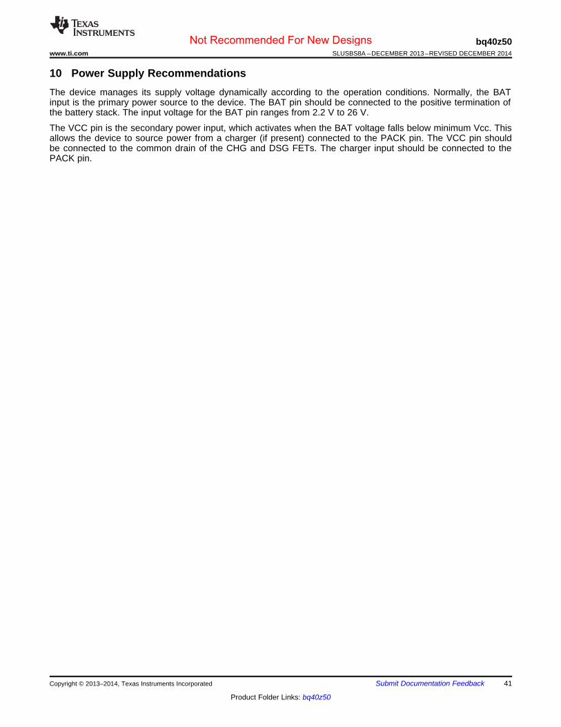
bq40z50www.ti.com SLUSBS8A –DECEMBER 2013–REVISED DECEMBER 2014
10 Power Supply RecommendationsThe device manages its supply voltage dynamically according to the operation conditions. Normally, the BATinput is the primary power source to the device. The BAT pin should be connected to the positive termination ofthe battery stack. The input voltage for the BAT pin ranges from 2.2 V to 26 V.
The VCC pin is the secondary power input, which activates when the BAT voltage falls below minimum Vcc. Thisallows the device to source power from a charger (if present) connected to the PACK pin. The VCC pin shouldbe connected to the common drain of the CHG and DSG FETs. The charger input should be connected to thePACK pin.
Copyright © 2013–2014, Texas Instruments Incorporated Submit Documentation Feedback 41
Product Folder Links: bq40z50
Not Recommended For New Designs
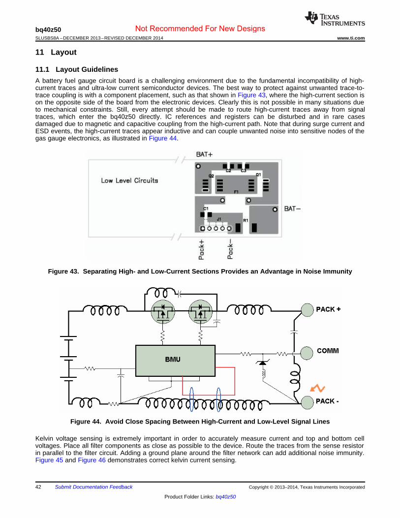
bq40z50SLUSBS8A –DECEMBER 2013–REVISED DECEMBER 2014 www.ti.com
11 Layout
11.1 Layout GuidelinesA battery fuel gauge circuit board is a challenging environment due to the fundamental incompatibility of high-current traces and ultra-low current semiconductor devices. The best way to protect against unwanted trace-to-trace coupling is with a component placement, such as that shown in Figure 43, where the high-current section ison the opposite side of the board from the electronic devices. Clearly this is not possible in many situations dueto mechanical constraints. Still, every attempt should be made to route high-current traces away from signaltraces, which enter the bq40z50 directly. IC references and registers can be disturbed and in rare casesdamaged due to magnetic and capacitive coupling from the high-current path. Note that during surge current andESD events, the high-current traces appear inductive and can couple unwanted noise into sensitive nodes of thegas gauge electronics, as illustrated in Figure 44.
Figure 43. Separating High- and Low-Current Sections Provides an Advantage in Noise Immunity
Figure 44. Avoid Close Spacing Between High-Current and Low-Level Signal Lines
Kelvin voltage sensing is extremely important in order to accurately measure current and top and bottom cellvoltages. Place all filter components as close as possible to the device. Route the traces from the sense resistorin parallel to the filter circuit. Adding a ground plane around the filter network can add additional noise immunity.Figure 45 and Figure 46 demonstrates correct kelvin current sensing.
42 Submit Documentation Feedback Copyright © 2013–2014, Texas Instruments Incorporated
Product Folder Links: bq40z50
Not Recommended For New Designs
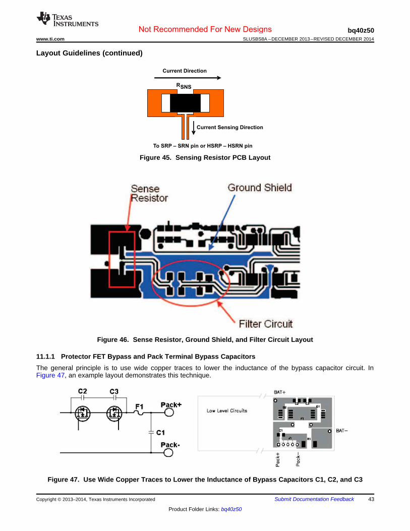
Current Direction
To SRP – SRN pin or HSRP – HSRN pin
RSNS
Current Sensing Direction
bq40z50www.ti.com SLUSBS8A –DECEMBER 2013–REVISED DECEMBER 2014
Layout Guidelines (continued)
Figure 45. Sensing Resistor PCB Layout
Figure 46. Sense Resistor, Ground Shield, and Filter Circuit Layout
11.1.1 Protector FET Bypass and Pack Terminal Bypass CapacitorsThe general principle is to use wide copper traces to lower the inductance of the bypass capacitor circuit. InFigure 47, an example layout demonstrates this technique.
Figure 47. Use Wide Copper Traces to Lower the Inductance of Bypass Capacitors C1, C2, and C3
Copyright © 2013–2014, Texas Instruments Incorporated Submit Documentation Feedback 43
Product Folder Links: bq40z50
Not Recommended For New Designs
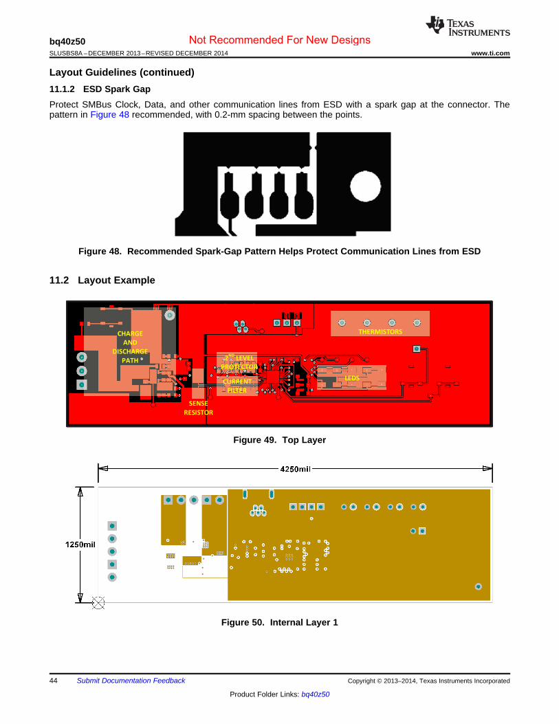
CHARGE
AND
DISCHARGE
PATH
CURRENT
FILTER
SENSE
RESISTOR
2ND
LEVEL
PROTECTOR
LEDS
THERMISTORS
bq40z50SLUSBS8A –DECEMBER 2013–REVISED DECEMBER 2014 www.ti.com
Layout Guidelines (continued)11.1.2 ESD Spark GapProtect SMBus Clock, Data, and other communication lines from ESD with a spark gap at the connector. Thepattern in Figure 48 recommended, with 0.2-mm spacing between the points.
Figure 48. Recommended Spark-Gap Pattern Helps Protect Communication Lines from ESD
11.2 Layout Example
Figure 49. Top Layer
Figure 50. Internal Layer 1
44 Submit Documentation Feedback Copyright © 2013–2014, Texas Instruments Incorporated
Product Folder Links: bq40z50
Not Recommended For New Designs
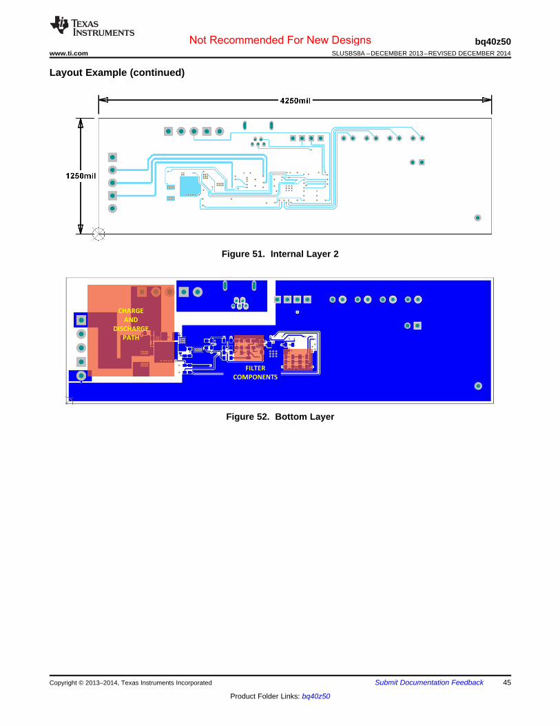
FILTER
COMPONENTS
CHARGE
AND
DISCHARGE
PATH
bq40z50www.ti.com SLUSBS8A –DECEMBER 2013–REVISED DECEMBER 2014
Layout Example (continued)
Figure 51. Internal Layer 2
Figure 52. Bottom Layer
Copyright © 2013–2014, Texas Instruments Incorporated Submit Documentation Feedback 45
Product Folder Links: bq40z50
Not Recommended For New Designs
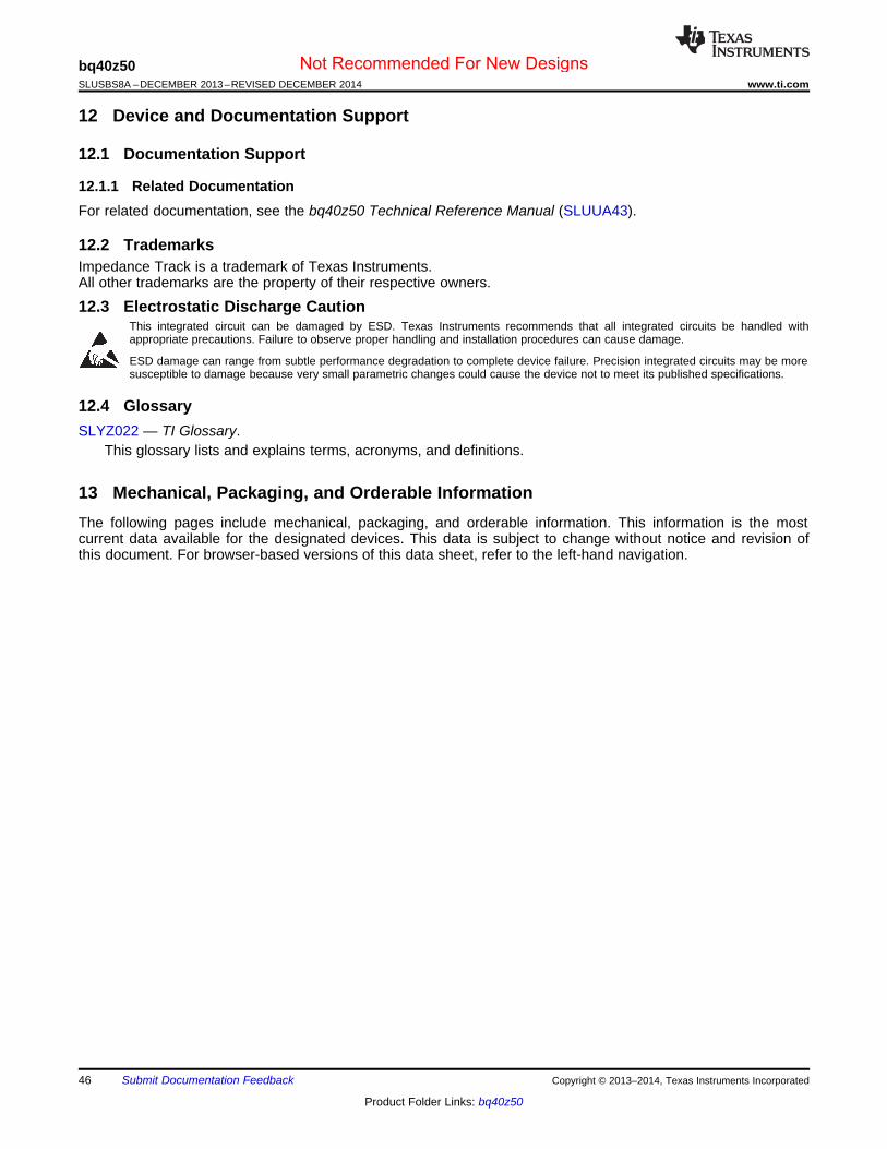
bq40z50SLUSBS8A –DECEMBER 2013–REVISED DECEMBER 2014 www.ti.com
12 Device and Documentation Support
12.1 Documentation Support
12.1.1 Related DocumentationFor related documentation, see the bq40z50 Technical Reference Manual (SLUUA43).
12.2 TrademarksImpedance Track is a trademark of Texas Instruments.All other trademarks are the property of their respective owners.
12.3 Electrostatic Discharge CautionThis integrated circuit can be damaged by ESD. Texas Instruments recommends that all integrated circuits be handled withappropriate precautions. Failure to observe proper handling and installation procedures can cause damage.
ESD damage can range from subtle performance degradation to complete device failure. Precision integrated circuits may be moresusceptible to damage because very small parametric changes could cause the device not to meet its published specifications.
12.4 GlossarySLYZ022 — TI Glossary.
This glossary lists and explains terms, acronyms, and definitions.
13 Mechanical, Packaging, and Orderable InformationThe following pages include mechanical, packaging, and orderable information. This information is the mostcurrent data available for the designated devices. This data is subject to change without notice and revision ofthis document. For browser-based versions of this data sheet, refer to the left-hand navigation.
46 Submit Documentation Feedback Copyright © 2013–2014, Texas Instruments Incorporated
Product Folder Links: bq40z50
Not Recommended For New Designs
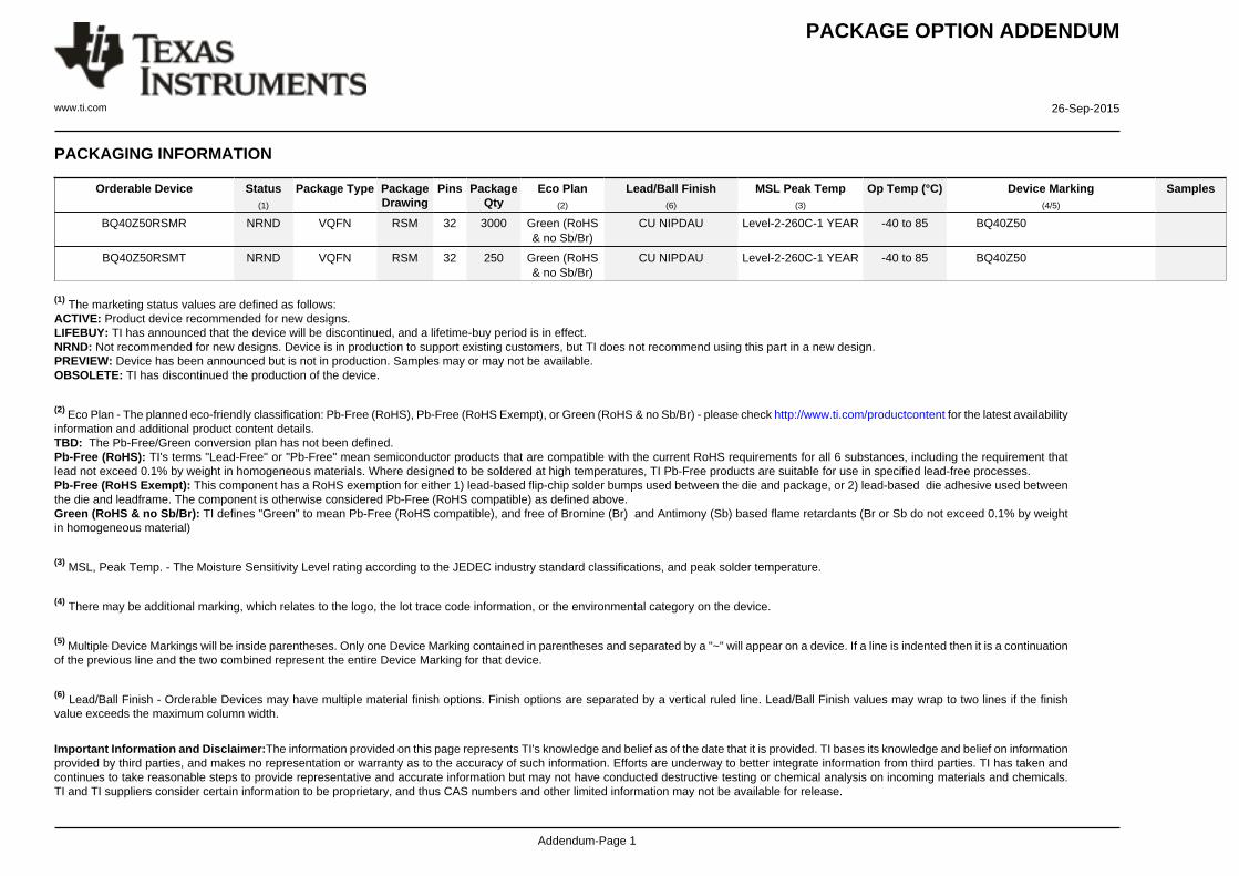
PACKAGE OPTION ADDENDUM
www.ti.com 26-Sep-2015
Addendum-Page 1
PACKAGING INFORMATION
Orderable Device Status(1)
Package Type PackageDrawing
Pins PackageQty
Eco Plan(2)
Lead/Ball Finish(6)
MSL Peak Temp(3)
Op Temp (°C) Device Marking(4/5)
Samples
BQ40Z50RSMR NRND VQFN RSM 32 3000 Green (RoHS& no Sb/Br)
CU NIPDAU Level-2-260C-1 YEAR -40 to 85 BQ40Z50
BQ40Z50RSMT NRND VQFN RSM 32 250 Green (RoHS& no Sb/Br)
CU NIPDAU Level-2-260C-1 YEAR -40 to 85 BQ40Z50
(1) The marketing status values are defined as follows:ACTIVE: Product device recommended for new designs.LIFEBUY: TI has announced that the device will be discontinued, and a lifetime-buy period is in effect.NRND: Not recommended for new designs. Device is in production to support existing customers, but TI does not recommend using this part in a new design.PREVIEW: Device has been announced but is not in production. Samples may or may not be available.OBSOLETE: TI has discontinued the production of the device.
(2) Eco Plan - The planned eco-friendly classification: Pb-Free (RoHS), Pb-Free (RoHS Exempt), or Green (RoHS & no Sb/Br) - please check http://www.ti.com/productcontent for the latest availabilityinformation and additional product content details.TBD: The Pb-Free/Green conversion plan has not been defined.Pb-Free (RoHS): TI's terms "Lead-Free" or "Pb-Free" mean semiconductor products that are compatible with the current RoHS requirements for all 6 substances, including the requirement thatlead not exceed 0.1% by weight in homogeneous materials. Where designed to be soldered at high temperatures, TI Pb-Free products are suitable for use in specified lead-free processes.Pb-Free (RoHS Exempt): This component has a RoHS exemption for either 1) lead-based flip-chip solder bumps used between the die and package, or 2) lead-based die adhesive used betweenthe die and leadframe. The component is otherwise considered Pb-Free (RoHS compatible) as defined above.Green (RoHS & no Sb/Br): TI defines "Green" to mean Pb-Free (RoHS compatible), and free of Bromine (Br) and Antimony (Sb) based flame retardants (Br or Sb do not exceed 0.1% by weightin homogeneous material)
(3) MSL, Peak Temp. - The Moisture Sensitivity Level rating according to the JEDEC industry standard classifications, and peak solder temperature.
(4) There may be additional marking, which relates to the logo, the lot trace code information, or the environmental category on the device.
(5) Multiple Device Markings will be inside parentheses. Only one Device Marking contained in parentheses and separated by a "~" will appear on a device. If a line is indented then it is a continuationof the previous line and the two combined represent the entire Device Marking for that device.
(6) Lead/Ball Finish - Orderable Devices may have multiple material finish options. Finish options are separated by a vertical ruled line. Lead/Ball Finish values may wrap to two lines if the finishvalue exceeds the maximum column width.
Important Information and Disclaimer:The information provided on this page represents TI's knowledge and belief as of the date that it is provided. TI bases its knowledge and belief on informationprovided by third parties, and makes no representation or warranty as to the accuracy of such information. Efforts are underway to better integrate information from third parties. TI has taken andcontinues to take reasonable steps to provide representative and accurate information but may not have conducted destructive testing or chemical analysis on incoming materials and chemicals.TI and TI suppliers consider certain information to be proprietary, and thus CAS numbers and other limited information may not be available for release.

PACKAGE OPTION ADDENDUM
www.ti.com 26-Sep-2015
Addendum-Page 2
In no event shall TI's liability arising out of such information exceed the total purchase price of the TI part(s) at issue in this document sold by TI to Customer on an annual basis.
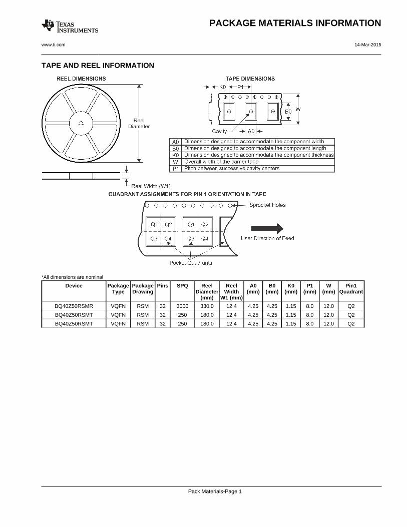
TAPE AND REEL INFORMATION
*All dimensions are nominal
Device PackageType
PackageDrawing
Pins SPQ ReelDiameter
(mm)
ReelWidth
W1 (mm)
A0(mm)
B0(mm)
K0(mm)
P1(mm)
W(mm)
Pin1Quadrant
BQ40Z50RSMR VQFN RSM 32 3000 330.0 12.4 4.25 4.25 1.15 8.0 12.0 Q2
BQ40Z50RSMT VQFN RSM 32 250 180.0 12.4 4.25 4.25 1.15 8.0 12.0 Q2
BQ40Z50RSMT VQFN RSM 32 250 180.0 12.4 4.25 4.25 1.15 8.0 12.0 Q2
PACKAGE MATERIALS INFORMATION
www.ti.com 14-Mar-2015
Pack Materials-Page 1
*All dimensions are nominal
Device Package Type Package Drawing Pins SPQ Length (mm) Width (mm) Height (mm)
BQ40Z50RSMR VQFN RSM 32 3000 367.0 367.0 35.0
BQ40Z50RSMT VQFN RSM 32 250 210.0 185.0 35.0
BQ40Z50RSMT VQFN RSM 32 250 210.0 185.0 35.0
PACKAGE MATERIALS INFORMATION
www.ti.com 14-Mar-2015
Pack Materials-Page 2
IMPORTANT NOTICE
Texas Instruments Incorporated and its subsidiaries (TI) reserve the right to make corrections, enhancements, improvements and otherchanges to its semiconductor products and services per JESD46, latest issue, and to discontinue any product or service per JESD48, latestissue. Buyers should obtain the latest relevant information before placing orders and should verify that such information is current andcomplete. All semiconductor products (also referred to herein as “components”) are sold subject to TI’s terms and conditions of salesupplied at the time of order acknowledgment.TI warrants performance of its components to the specifications applicable at the time of sale, in accordance with the warranty in TI’s termsand conditions of sale of semiconductor products. Testing and other quality control techniques are used to the extent TI deems necessaryto support this warranty. Except where mandated by applicable law, testing of all parameters of each component is not necessarilyperformed.TI assumes no liability for applications assistance or the design of Buyers’ products. Buyers are responsible for their products andapplications using TI components. To minimize the risks associated with Buyers’ products and applications, Buyers should provideadequate design and operating safeguards.TI does not warrant or represent that any license, either express or implied, is granted under any patent right, copyright, mask work right, orother intellectual property right relating to any combination, machine, or process in which TI components or services are used. Informationpublished by TI regarding third-party products or services does not constitute a license to use such products or services or a warranty orendorsement thereof. Use of such information may require a license from a third party under the patents or other intellectual property of thethird party, or a license from TI under the patents or other intellectual property of TI.Reproduction of significant portions of TI information in TI data books or data sheets is permissible only if reproduction is without alterationand is accompanied by all associated warranties, conditions, limitations, and notices. TI is not responsible or liable for such altereddocumentation. Information of third parties may be subject to additional restrictions.Resale of TI components or services with statements different from or beyond the parameters stated by TI for that component or servicevoids all express and any implied warranties for the associated TI component or service and is an unfair and deceptive business practice.TI is not responsible or liable for any such statements.Buyer acknowledges and agrees that it is solely responsible for compliance with all legal, regulatory and safety-related requirementsconcerning its products, and any use of TI components in its applications, notwithstanding any applications-related information or supportthat may be provided by TI. Buyer represents and agrees that it has all the necessary expertise to create and implement safeguards whichanticipate dangerous consequences of failures, monitor failures and their consequences, lessen the likelihood of failures that might causeharm and take appropriate remedial actions. Buyer will fully indemnify TI and its representatives against any damages arising out of the useof any TI components in safety-critical applications.In some cases, TI components may be promoted specifically to facilitate safety-related applications. With such components, TI’s goal is tohelp enable customers to design and create their own end-product solutions that meet applicable functional safety standards andrequirements. Nonetheless, such components are subject to these terms.No TI components are authorized for use in FDA Class III (or similar life-critical medical equipment) unless authorized officers of the partieshave executed a special agreement specifically governing such use.Only those TI components which TI has specifically designated as military grade or “enhanced plastic” are designed and intended for use inmilitary/aerospace applications or environments. Buyer acknowledges and agrees that any military or aerospace use of TI componentswhich have not been so designated is solely at the Buyer's risk, and that Buyer is solely responsible for compliance with all legal andregulatory requirements in connection with such use.TI has specifically designated certain components as meeting ISO/TS16949 requirements, mainly for automotive use. In any case of use ofnon-designated products, TI will not be responsible for any failure to meet ISO/TS16949.
Products ApplicationsAudio www.ti.com/audio Automotive and Transportation www.ti.com/automotiveAmplifiers amplifier.ti.com Communications and Telecom www.ti.com/communicationsData Converters dataconverter.ti.com Computers and Peripherals www.ti.com/computersDLP® Products www.dlp.com Consumer Electronics www.ti.com/consumer-appsDSP dsp.ti.com Energy and Lighting www.ti.com/energyClocks and Timers www.ti.com/clocks Industrial www.ti.com/industrialInterface interface.ti.com Medical www.ti.com/medicalLogic logic.ti.com Security www.ti.com/securityPower Mgmt power.ti.com Space, Avionics and Defense www.ti.com/space-avionics-defenseMicrocontrollers microcontroller.ti.com Video and Imaging www.ti.com/videoRFID www.ti-rfid.comOMAP Applications Processors www.ti.com/omap TI E2E Community e2e.ti.comWireless Connectivity www.ti.com/wirelessconnectivity
Mailing Address: Texas Instruments, Post Office Box 655303, Dallas, Texas 75265Copyright © 2015, Texas Instruments Incorporated