Embed Size (px)
Citation preview
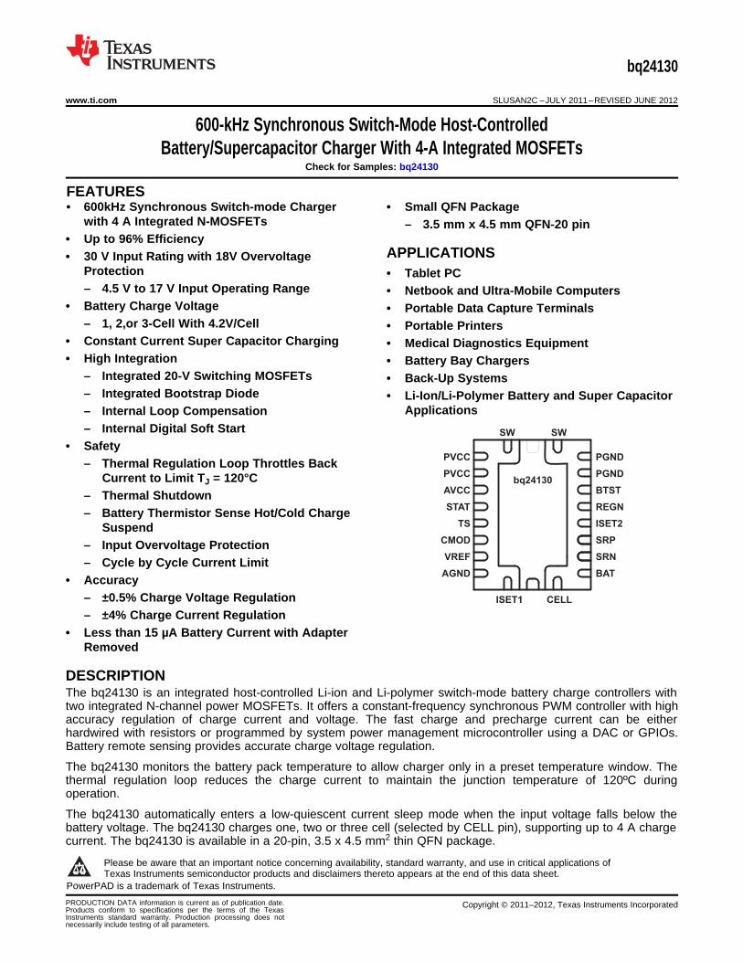
bq24130PVCC
SW
CELLISET1
SW
STAT
PVCC
AGND
AVCC
TS
CMOD
VREF
PGND
REGN
PGND
BAT
BTST
ISET2
SRP
SRN
bq24130
www.ti.com SLUSAN2C –JULY 2011–REVISED JUNE 2012
600-kHz Synchronous Switch-Mode Host-ControlledBattery/Supercapacitor Charger With 4-A Integrated MOSFETs
Check for Samples: bq24130
1FEATURES2• 600kHz Synchronous Switch-mode Charger • Small QFN Package
with 4 A Integrated N-MOSFETs – 3.5 mm x 4.5 mm QFN-20 pin• Up to 96% Efficiency
APPLICATIONS• 30 V Input Rating with 18V OvervoltageProtection • Tablet PC– 4.5 V to 17 V Input Operating Range • Netbook and Ultra-Mobile Computers
• Battery Charge Voltage • Portable Data Capture Terminals– 1, 2,or 3-Cell With 4.2V/Cell • Portable Printers
• Constant Current Super Capacitor Charging • Medical Diagnostics Equipment• High Integration • Battery Bay Chargers
– Integrated 20-V Switching MOSFETs • Back-Up Systems– Integrated Bootstrap Diode • Li-Ion/Li-Polymer Battery and Super Capacitor
Applications– Internal Loop Compensation– Internal Digital Soft Start
• Safety– Thermal Regulation Loop Throttles Back
Current to Limit TJ = 120°C– Thermal Shutdown– Battery Thermistor Sense Hot/Cold Charge
Suspend– Input Overvoltage Protection– Cycle by Cycle Current Limit
• Accuracy– ±0.5% Charge Voltage Regulation– ±4% Charge Current Regulation
• Less than 15 µA Battery Current with AdapterRemoved
DESCRIPTIONThe bq24130 is an integrated host-controlled Li-ion and Li-polymer switch-mode battery charge controllers withtwo integrated N-channel power MOSFETs. It offers a constant-frequency synchronous PWM controller with highaccuracy regulation of charge current and voltage. The fast charge and precharge current can be eitherhardwired with resistors or programmed by system power management microcontroller using a DAC or GPIOs.Battery remote sensing provides accurate charge voltage regulation.
The bq24130 monitors the battery pack temperature to allow charger only in a preset temperature window. Thethermal regulation loop reduces the charge current to maintain the junction temperature of 120ºC duringoperation.
The bq24130 automatically enters a low-quiescent current sleep mode when the input voltage falls below thebattery voltage. The bq24130 charges one, two or three cell (selected by CELL pin), supporting up to 4 A chargecurrent. The bq24130 is available in a 20-pin, 3.5 x 4.5 mm2 thin QFN package.1
Please be aware that an important notice concerning availability, standard warranty, and use in critical applications ofTexas Instruments semiconductor products and disclaimers thereto appears at the end of this data sheet.
2PowerPAD is a trademark of Texas Instruments.
PRODUCTION DATA information is current as of publication date. Copyright © 2011–2012, Texas Instruments IncorporatedProducts conform to specifications per the terms of the TexasInstruments standard warranty. Production processing does notnecessarily include testing of all parameters.
( )(PRECHG)
(SR)
ISET2V
I =100 R´
( )(CHG)
(SR)
ISET1V
I =20 R´
bq24130
SLUSAN2C –JULY 2011–REVISED JUNE 2012 www.ti.com
These devices have limited built-in ESD protection. The leads should be shorted together or the device placed in conductive foamduring storage or handling to prevent electrostatic damage to the MOS gates.
PIN FUNCTIONSPIN NAME TYPE FUNCTION DESCRIPTION
Switching node, charge current output inductor connection. Connect the 0.47-µF bootstrap capacitor from1, 20 SW P SW to BTST.
Charger input voltage. Connect at least 10-µF ceramic capacitor from PVCC to PGND and place it as2, 3 PVCC P close as possible to IC.
IC power positive supply. Place a 1-µF ceramic capacitor from AVCC to AGND and place it as close as4 AVCC P possible to IC. Place a 10 ohm resistor from input side to AVCC pin to filter the noise. For 5 V input, a 5-Ω
resistor is recommended.
Open-drain charge status pin with 10-kΩ pull up to power rail. The STAT pin can be used to drive LED orcommunicate with the host processor. It indicates various charger operations: LOW when charge in5 STAT O process, HIGH when charge complete or SLEEP mode. Blinking when fault occurs, such as chargesuspend, and input overvoltage.
Temperature qualification voltage input. Connect a negative temperature coefficient thermistor. Program6 TS I the hot and cold temperature window with a resistor divider from VREF to TS to AGND. The temperature
qualification window can be set to 5-40ºC or wider. The 103AT thermister is recommended.
Charge mode selection: low (pull down to AGND) for pre-charge current as set by ISET2 pin and high (pull7 CMOD I up to VREF) for fast charge current as set by ISET1 pin. If the battery voltage reaches the voltage
regulation set point, IC changes to voltage regulation mode regardless of CMOD pin input.
3.3 V reference voltage output. Place a 1-µF ceramic capacitor from VREF to AGND pin close to the IC.8 VREF P This voltage could be used for programming charge current regulation on ISET1 and ISET2 pins,
programming the threshold of TS pin, and the pull-up rail of STAT pin and CELL pin.
Analog ground. Ground connection for low-current sensitive analog and digital signals. On PCB layout,9 AGND P connect to the analog ground plane, and only connect to PGND through the PowerPad underneath the IC.
Fast charge current set point. Use a voltage divider from VREF to AGND to set this value.
10 ISET1 I
The charger is disabled when ISET1 pin voltage is below 50mV and is enabled when ISET1 pin voltage isabove 100mV.
11 CELL I Cell selection pin. Set CELL pin LO for 1-cell, Float for 2-cell, and HI for 3-cell with a fixed 4.2 V per cell.
Battery voltage remote sense. Directly connect a kelvin sense trace from the battery pack positive terminal12 BAT I to the BAT pin to accurately sense the battery pack voltage. Place a 0.1-µF capacitor from BAT to AGND
close to the IC to filter high frequency noise.
Charge current sense resistor, negative input. A 0.1-µF ceramic capacitor is placed from SRN to SRP to13 SRN I provide differential-mode filtering. A 0.1-µF ceramic capacitor is placed from SRN pin to AGND for
common-mode filtering.
Charge current sense resistor, positive input. A 0.1-µF ceramic capacitor is placed from SRN to SRP to14 SRP P/I provide differential-mode filtering. A 0.1-µF ceramic capacitor is placed from SRP pin to AGND for
common-mode filtering.
Pre-charge current set point. Use a voltage divider from VREF to AGND to set this value.
15 ISET2 I
PWM low side driver positive 6V supply output. Connect a 1-µF ceramic capacitor from REGN to PGND16 REGN P pin, close to the IC. Use for low side driver and high-side driver bootstrap voltage by integrated diode from
REGN to BTST.
17 BTST P PWM high side driver positive supply. Connect the 47 nF bootstrap capacitor from SW to BTST.
Power ground. Ground connection for high-current power converter node. On PCB layout, connect directly18, 19 PGND to source of low-side power MOSFET, to ground connection of in put and output capacitors of the charger.
Only connect to AGND through the PowerPAD underneath the IC.
Exposed pad beneath the IC. Always solder PowerPAD to the board, and have vias on the PowerPADPowerPAD™ Pad Pad plane star-connecting to AGND and ground plane for high-current power converter. It also serves as a
thermal pad to dissipate the heat.
ORDERING INFORMATION (1)
PART NUMBER MARKING PACKAGE ORDERING NUMBER QUANTITY
bq24130RHLR 3000bq24130 bq24130 20-pin 3.5 x 4.5mm2 QFN
bq24130RHLT 250
(1) For the most current package and ordering information, see the Package Option Addendum at the end of this document, or see the TIwebsite at www.ti.com.
2 Submit Documentation Feedback Copyright © 2011–2012, Texas Instruments Incorporated
Product Folder Link(s): bq24130
bq24130
www.ti.com SLUSAN2C –JULY 2011–REVISED JUNE 2012
ABSOLUTE MAXIMUM RATINGS (1) (2)
over operating free-air temperature range (unless otherwise noted)
VALUE UNIT
MIN MAX
PVCC –0.3 20 V
AVCC, STAT –0.3 30 V
SRP, SRN, BAT –0.3 20 VVoltage(with respect to AGND and SW –2 20 VPGND) REGN, TS, CELL, CMOD –0.3 7 V
BTST –0.3 26 V
VREF, ISET1, ISET2 –0.3 3.6 V
Maximum difference voltage SRP–SRN –0.5 0.5 V
Junction temperature, TJ –40 155 °C
Storage temperature, Tstg –55 155 °C
(1) Stresses beyond those listed under absolute maximum ratings may cause permanent damage to the device. These are stress ratingsonly, and functional operation of the device at these or any other conditions beyond those indicated under recommended operatingconditions is not implied. Exposure to absolute-maximum-rated conditions for extended periods may affect device reliability. All voltagevalues are with respect to the network ground terminal unless otherwise noted.
(2) All voltages are with respect to GND if not specified. Currents are positive into, negative out of the specified terminal, if not specified.Consult Packaging Section of the data sheet for thermal limitations and considerations of packages.
THERMAL INFORMATIONbq24130
THERMAL METRIC (1) (2) UNITSRHL (20 PIN)
θJA Junction-to-ambient thermal resistance 35
θJCtop Junction-to-case (top) thermal resistance N/A
θJB Junction-to-board thermal resistance N/A °C/W
ψJT Junction-to-top characterization parameter 0.4
ψJB Junction-to-board characterization parameter 9.1
θJCbot Junction-to-case (bottom) thermal resistance 2.1
(1) For more information about traditional and new thermal metrics, see the IC Package Thermal Metrics application report, SPRA953.(2) For thermal estimates of this device based on PCB copper area, see the TI PCB Thermal Calculator.RECOMMENDED OPERATING CONDITIONS
MIN MAX UNIT
Input voltage VIN 4.5 17 V
Output voltage BAT 13.5 V
Output current IOUT 0.6 4 A
Maximum difference voltage SRP-SRN –200 200 mV
Operating junction temperature range TJ –40 125 °C
Copyright © 2011–2012, Texas Instruments Incorporated Submit Documentation Feedback 3
Product Folder Link(s): bq24130
bq24130
SLUSAN2C –JULY 2011–REVISED JUNE 2012 www.ti.com
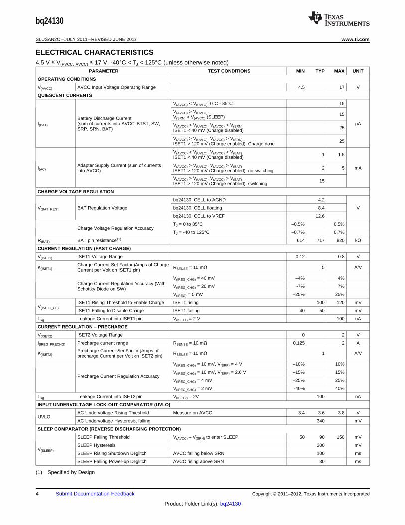
ELECTRICAL CHARACTERISTICS4.5 V ≤ V(PVCC, AVCC) ≤ 17 V, -40°C < TJ < 125°C (unless otherwise noted)
PARAMETER TEST CONDITIONS MIN TYP MAX UNIT
OPERATING CONDITIONS
V(AVCC) AVCC Input Voltage Operating Range 4.5 17 V
QUIESCENT CURRENTS
V(AVCC) < V(UVLO), 0°C - 85°C 15
V(AVCC) > V(UVLO) 15V(SRN) > V(AVCC) (SLEEP)Battery Discharge CurrentI(BAT) (sum of currents into AVCC, BTST, SW, µAV(AVCC) > V(UVLO), V(AVCC) > V(SRN) 25SRP, SRN, BAT) ISET1 < 40 mV (Charge disabled)
V(AVCC) > V(UVLO), V(AVCC) > V(SRN) 25ISET1 > 120 mV (Charge enabled), Charge done
V(AVCC) > V(UVLO), V(AVCC) > V(BAT) 1 1.5ISET1 < 40 mV (Charge disabled)
Adapter Supply Current (sum of currents V(AVCC) > V(UVLO), V(AVCC) > V(BAT)I(AC) 2 5 mAinto AVCC) ISET1 > 120 mV (Charge enabled), no switching
V(AVCC) > V(UVLO), V(AVCC) > V(BAT) 15ISET1 > 120 mV (Charge enabled), switching
CHARGE VOLTAGE REGULATION
bq24130, CELL to AGND 4.2
V(BAT_REG) BAT Regulation Voltage bq24130, CELL floating 8.4 V
bq24130, CELL to VREF 12.6
TJ = 0 to 85°C –0.5% 0.5%Charge Voltage Regulation Accuracy
TJ = -40 to 125°C –0.7% 0.7%
R(BAT) BAT pin resistance (1) 614 717 820 kΩ
CURRENT REGULATION (FAST CHARGE)
V(ISET1) ISET1 Voltage Range 0.12 0.8 V
Charge Current Set Factor (Amps of ChargeK(ISET1) RSENSE = 10 mΩ 5 A/VCurrent per Volt on ISET1 pin)
V(IREG_CHG) = 40 mV –4% 4%Charge Current Regulation Accuracy (With V(IREG_CHG) = 20 mV -7% 7%Schottky Diode on SW)
V(IREG) = 5 mV –25% 25%
ISET1 Rising Threshold to Enable Charge ISET1 rising 100 120 mVV(ISET1_CE)
ISET1 Falling to Disable Charge ISET1 falling 40 50 mV
lLkg Leakage Current into ISET1 pin V(ISET1) = 2 V 100 nA
CURRENT REGULATION – PRECHARGE
V(ISET2) ISET2 Voltage Range 0 2 V
I(IREG_PRECHG) Precharge current range RSENSE = 10 mΩ 0.125 2 A
Precharge Current Set Factor (Amps ofK(ISET2) RSENSE = 10 mΩ 1 A/Vprecharge Current per Volt on ISET2 pin)
V(IREG_CHG) = 10 mV, V(SRP) = 4 V –10% 10%
V(IREG_CHG) = 10 mV, V(SRP) = 2.6 V –15% 15%Precharge Current Regulation Accuracy
V(IREG_CHG) = 4 mV –25% 25%
V(IREG_CHG) = 2 mV -40% 40%
lLkg Leakage Current into ISET2 pin V(ISET2) = 2V 100 nA
INPUT UNDERVOLTAGE LOCK-OUT COMPARATOR (UVLO)
AC Undervoltage Rising Threshold Measure on AVCC 3.4 3.6 3.8 VUVLO
AC Undervoltage Hysteresis, falling 340 mV
SLEEP COMPARATOR (REVERSE DISCHARGING PROTECTION)
SLEEP Falling Threshold V(AVCC) – V(SRN) to enter SLEEP 50 90 150 mV
SLEEP Hysteresis 200 mVV(SLEEP)
SLEEP Rising Shutdown Deglitch AVCC falling below SRN 100 ms
SLEEP Falling Power-up Deglitch AVCC rising above SRN 30 ms
(1) Specified by Design
4 Submit Documentation Feedback Copyright © 2011–2012, Texas Instruments Incorporated
Product Folder Link(s): bq24130
bq24130
www.ti.com SLUSAN2C –JULY 2011–REVISED JUNE 2012
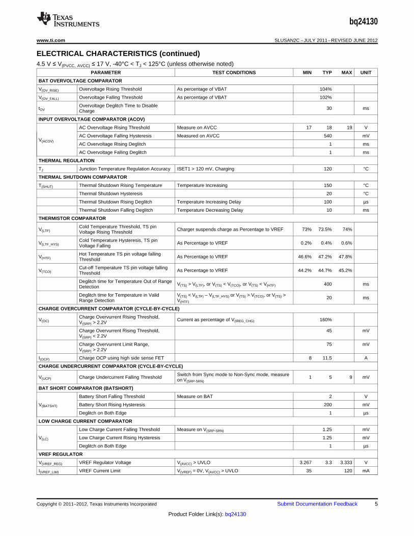
ELECTRICAL CHARACTERISTICS (continued)4.5 V ≤ V(PVCC, AVCC) ≤ 17 V, -40°C < TJ < 125°C (unless otherwise noted)
PARAMETER TEST CONDITIONS MIN TYP MAX UNIT
BAT OVERVOLTAGE COMPARATOR
V(OV_RISE) Overvoltage Rising Threshold As percentage of VBAT 104%
V(OV_FALL) Overvoltage Falling Threshold As percentage of VBAT 102%
Overvoltage Deglitch Time to DisabletOV 30 msCharge
INPUT OVERVOLTAGE COMPARATOR (ACOV)
AC Overvoltage Rising Threshold Measure on AVCC 17 18 19 V
AC Overvoltage Falling Hysteresis Measured on AVCC 540 mVV(ACOV)
AC Overvoltage Rising Deglitch 1 ms
AC Overvoltage Falling Deglitch 1 ms
THERMAL REGULATION
TJ Junction Temperature Regulation Accuracy ISET1 > 120 mV, Charging 120 °C
THERMAL SHUTDOWN COMPARATOR
T(SHUT) Thermal Shutdown Rising Temperature Temperature Increasing 150 °C
Thermal Shutdown Hysteresis 20 °C
Thermal Shutdown Rising Deglitch Temperature Increasing Delay 100 µs
Thermal Shutdown Falling Deglitch Temperature Decreasing Delay 10 ms
THERMISTOR COMPARATOR
Cold Temperature Threshold, TS pinV(LTF) Charger suspends charge as Percentage to VREF 73% 73.5% 74%Voltage Rising Threshold
Cold Temperature Hysteresis, TS pinV(LTF_HYS) As Percentage to VREF 0.2% 0.4% 0.6%Voltage Falling
Hot Temperature TS pin voltage fallingV(HTF) As Percentage to VREF 46.6% 47.2% 47.8%Threshold
Cut-off Temperature TS pin voltage fallingV(TCO) As Percentage to VREF 44.2% 44.7% 45.2%Threshold
Deglitch time for Temperature Out of Range V(TS) > V(LTF), or V(TS) < V(TCO), or V(TS) < V(HTF) 400 msDetection
Deglitch time for Temperature in Valid V(TS) < V(LTF) – V(LTF_HYS) or V(TS) > V(TCO), or V(TS) > 20 msRange Detection V(HTF)
CHARGE OVERCURRENT COMPARATOR (CYCLE-BY-CYCLE)
Charge Overvurrent Rising Threshold,V(OC) Current as percentage of V(IREG_CHG) 160%V(SRP) > 2.2V
Charge Overvurrent Rising Threshold, 45 mVV(SRP) < 2.2V
Charge Overvurrent Limit Range, 75 mVV(SRP) > 2.2V
I(OCP) Charge OCP using high side sense FET 8 11.5 A
CHARGE UNDERCURRENT COMPARATOR (CYCLE-BY-CYCLE)
Switch from Sync mode to Non-Sync mode, measureV(UCP) Charge Undercurrent Falling Threshold 1 5 9 mVon V(SRP-SRN)
BAT SHORT COMPARATOR (BATSHORT)
Battery Short Falling Threshold Measure on BAT 2 V
V(BATSHT) Battery Short Rising Hysteresis 200 mV
Deglitch on Both Edge 1 µs
LOW CHARGE CURRENT COMPARATOR
Low Charge Current Falling Threshold Measure on V(SRP-SRN) 1.25 mV
V(LC) Low Charge Current Rising Hysteresis 1.25 mV
Deglitch on Both Edge 1 µs
VREF REGULATOR
V(VREF_REG) VREF Regulator Voltage V(AVCC) > UVLO 3.267 3.3 3.333 V
I(VREF_LIM) VREF Current Limit V(VREF) = 0V, V(AVCC) > UVLO 35 120 mA
Copyright © 2011–2012, Texas Instruments Incorporated Submit Documentation Feedback 5
Product Folder Link(s): bq24130
bq24130
SLUSAN2C –JULY 2011–REVISED JUNE 2012 www.ti.com
ELECTRICAL CHARACTERISTICS (continued)4.5 V ≤ V(PVCC, AVCC) ≤ 17 V, -40°C < TJ < 125°C (unless otherwise noted)
PARAMETER TEST CONDITIONS MIN TYP MAX UNIT
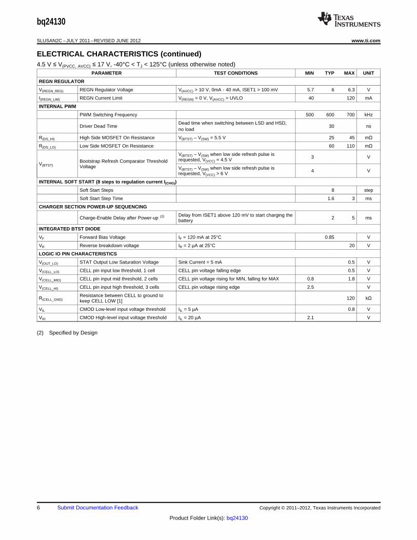
REGN REGULATOR
V(REGN_REG) REGN Regulator Voltage V(AVCC) > 10 V, 0mA - 40 mA, ISET1 > 100 mV 5.7 6 6.3 V
I(REGN_LIM) REGN Current Limit V(REGN) = 0 V, V(AVCC) > UVLO 40 120 mA
INTERNAL PWM
PWM Switching Frequency 500 600 700 kHz
Dead time when switching between LSD and HSD,Driver Dead Time 30 ns
no load
R(DS_HI) High Side MOSFET On Resistance V(BTST) – V(SW) = 5.5 V 25 45 mΩ
R(DS_LO) Low Side MOSFET On Resistance 60 110 mΩ
V(BTST) – V(SW) when low side refresh pulse is 3 Vrequested, V(VCC) = 4.5 VBootstrap Refresh Comparator ThresholdV(BTST) Voltage V(BTST) – V(SW) when low side refresh pulse is 4 Vrequested, V(VCC) > 6 V
INTERNAL SOFT START (8 steps to regulation current I(CHG))
Soft Start Steps 8 step
Soft Start Step Time 1.6 3 ms
CHARGER SECTION POWER-UP SEQUENCING
Delay from ISET1 above 120 mV to start charging theCharge-Enable Delay after Power-up (2) 2 5 msbattery
INTEGRATED BTST DIODE
VF Forward Bias Voltage IF = 120 mA at 25°C 0.85 V
VR Reverse breakdown voltage IR = 2 µA at 25°C 20 V
LOGIC IO PIN CHARACTERISTICS
V(OUT_LO) STAT Output Low Saturation Voltage Sink Current = 5 mA 0.5 V
V(CELL_LO) CELL pin input low threshold, 1 cell CELL pin voltage falling edge 0.5 V
V(CELL_MID) CELL pin input mid threshold, 2 cells CELL pin voltage rising for MIN, falling for MAX 0.8 1.8 V
V(CELL_HI) CELL pin input high threshold, 3 cells CELL pin voltage rising edge 2.5 V
Resistance between CELL to ground toR(CELL_GND) 120 kΩkeep CELL LOW [1]
VIL CMOD Low-level input voltage threshold IIL = 5 µA 0.8 V
VIH CMOD High-level input voltage threshold IIL = 20 µA 2.1 V
(2) Specified by Design
6 Submit Documentation Feedback Copyright © 2011–2012, Texas Instruments Incorporated
Product Folder Link(s): bq24130
AVCC
VUVLO
UVLO
VSRN+VSLEEP_FALL
SLEEP
VREF
LDO
VREF
LDO
EN_VREFVREF
VACOV
ACOV
BAT
ISET1
ISET2
Selection
ISET1
ISET2
SRP
SRN
V(SRP-SRN)
IBAT_REG
20μA
1V
20μA
FBO EAI
EAO
VOV_RISE
BAT_OVP
PWM
PWM
CONTROL
LOGIC
AGND
LEVEL
SHIFTER
LEVEL
SHIFTER
PVCC
PVCC
SW
SW
PGND
PGND
REGNTJ_REG
IC TJ
BTST
REGNREGN
LDO
REGN
LDOEN_CHRG
SYNCV(SRP-SRN)
VUCP
REFRESH
VBTST
VSW+VBTST_REFRESH
LC
V(SRP-SRN)
VLC
OCP V(SRP-SRN)
VOC
BAT_SHTVBAT_SHT
STAT
CHARGE
TSHUT
TSHUT
IC TJ STATE
MACHINE
LOGIC
CMOD
ACOV
UVLO
SLEEP
ACOV
UVLO
SLEEP
/STAT
CMOD
2.1V
120mV
EN_CHRG
bq24130
20X
LTF
VREF
HTF
TCO
TS
SUSPEND
LTF
VREF
HTF
TCO
TS
SUSPEND
EN_CHRG
CELL
bq24130
www.ti.com SLUSAN2C –JULY 2011–REVISED JUNE 2012
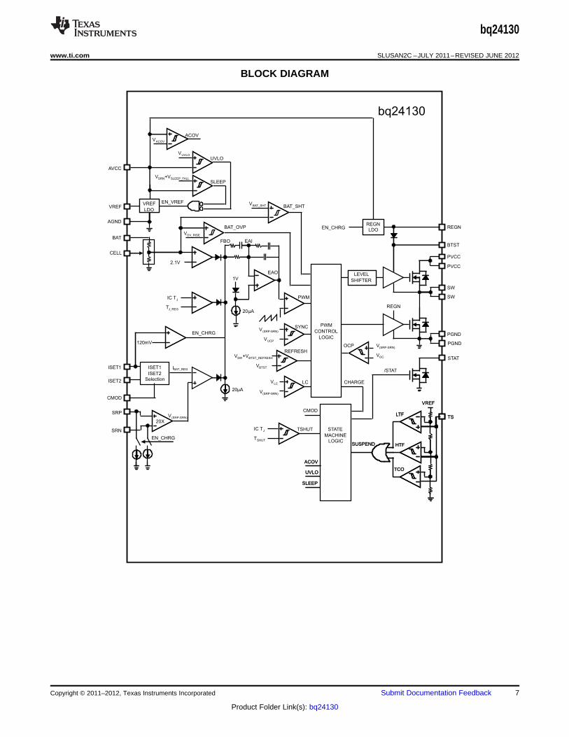
BLOCK DIAGRAM
Copyright © 2011–2012, Texas Instruments Incorporated Submit Documentation Feedback 7
Product Folder Link(s): bq24130
L: 4.7?H
ADAPTER
RT
103AT
C9, C10
2 x 10?
VBATSW
BTST
REGN
PGND
C5
47n
AVCC
ISET2
VREF
CMOD
SRN
TS
SRP
BAT
PVCC
C7
0.1?
C4
10µ
C2: 1µ
C1
1µ
C6
1?
VREF
R1
10
R4
154k
R5
10k
R6
5.23k
R7
30.1k
STAT
R9:10m
Q2
Q1
ISET1
AGND
C8
0.1?
R8
1.5k
CELL
R2
100k
R3
22.2k
D1
bq24130
Q3 Q4
Q6
ISET1<40mV
Charge Diable
CMODHigh: Fast charge ISET1
Low: Pre-charge ISET2
D2
(optional)
SYSTEM
bq24130
SLUSAN2C –JULY 2011–REVISED JUNE 2012 www.ti.com
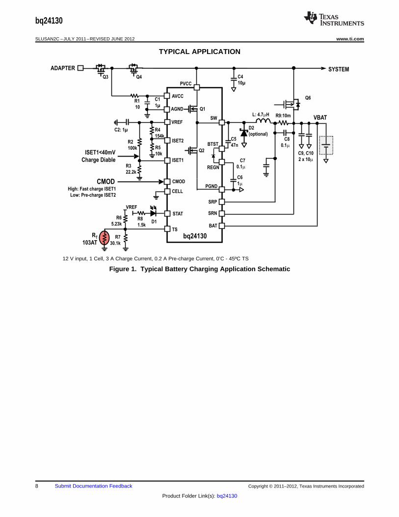
TYPICAL APPLICATION
12 V input, 1 Cell, 3 A Charge Current, 0.2 A Pre-charge Current, 0’C - 45ºC TS
Figure 1. Typical Battery Charging Application Schematic
8 Submit Documentation Feedback Copyright © 2011–2012, Texas Instruments Incorporated
Product Folder Link(s): bq24130
L: 4.7?H
ADAPTER
RT
103AT
C9, C10
2 x 10?
VCAPSW
BTST
REGN
PGND
C5
47n
AVCC
ISET2
VREF
CMOD
SRN
TS
SRP
BAT
PVCC
C7
0.1?
C4
10µ
C2: 1µ
C1
1µ
VREF
R1
10
R4
65k
R5
100k
R6
2.98k
R7
11.84k
STAT
R9:10m
Q2
Q1
ISET1
AGND
C8
0.1?
R8
1.5k
CELL
R2
232k
R3
32.4k
D1
bq24130
ISET1<40mV
Charge Diable
R12
60k
R11
300k
C6
1?
bq24130
www.ti.com SLUSAN2C –JULY 2011–REVISED JUNE 2012
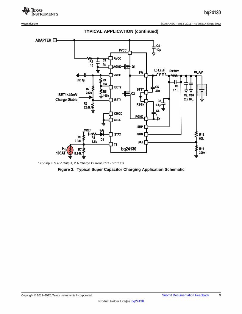
TYPICAL APPLICATION (continued)
12 V input, 5.4 V Output, 2 A Charge Current, 0°C - 60°C TS
Figure 2. Typical Super Capacitor Charging Application Schematic
Copyright © 2011–2012, Texas Instruments Incorporated Submit Documentation Feedback 9
Product Folder Link(s): bq24130
t - Time - 4 ms/div
ICHG
2 A/div
PH
10 V/div
ISET1500 mV/div
STAT10 V/div
t - Time - 10 ms/div
I(IND)2 A/div
PH10 V/div
AVCC
10 V/div
REGN
5 V/div
BAT
5 V/div
STAT
10 V/div
t - Time - 10 ms/div
AVCC
10 V/div
REGN
5 V/div
ICHG
2 A/div
t - Time - 10 ms/div
PH 10 V/div
bq24130
SLUSAN2C –JULY 2011–REVISED JUNE 2012 www.ti.com
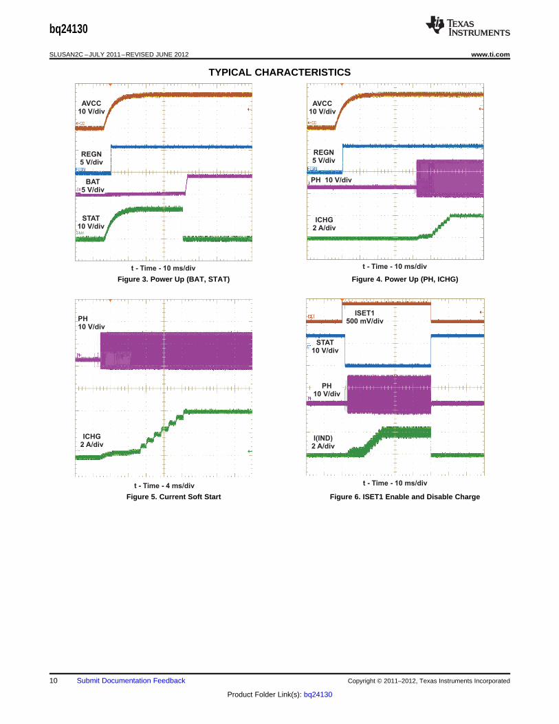
TYPICAL CHARACTERISTICS
Figure 3. Power Up (BAT, STAT) Figure 4. Power Up (PH, ICHG)
Figure 5. Current Soft Start Figure 6. ISET1 Enable and Disable Charge
10 Submit Documentation Feedback Copyright © 2011–2012, Texas Instruments Incorporated
Product Folder Link(s): bq24130
t - Time - 10 ms/div
ICHG
2 A/div
CMOD
5 V/div
t - Time - 400 ns/div
ICHG
1 A/div
PH
10 V/div
STAT10 V/div
t - Time - 2 s/divm
I(IND)2 A/div
PH 10 V/div
ISET1500 mV/div
STAT
10 V/div
t - Time - 4 ms/div
ICHG
2 A/div
PH
10 V/div
ISET1
500 mV/div
bq24130
www.ti.com SLUSAN2C –JULY 2011–REVISED JUNE 2012
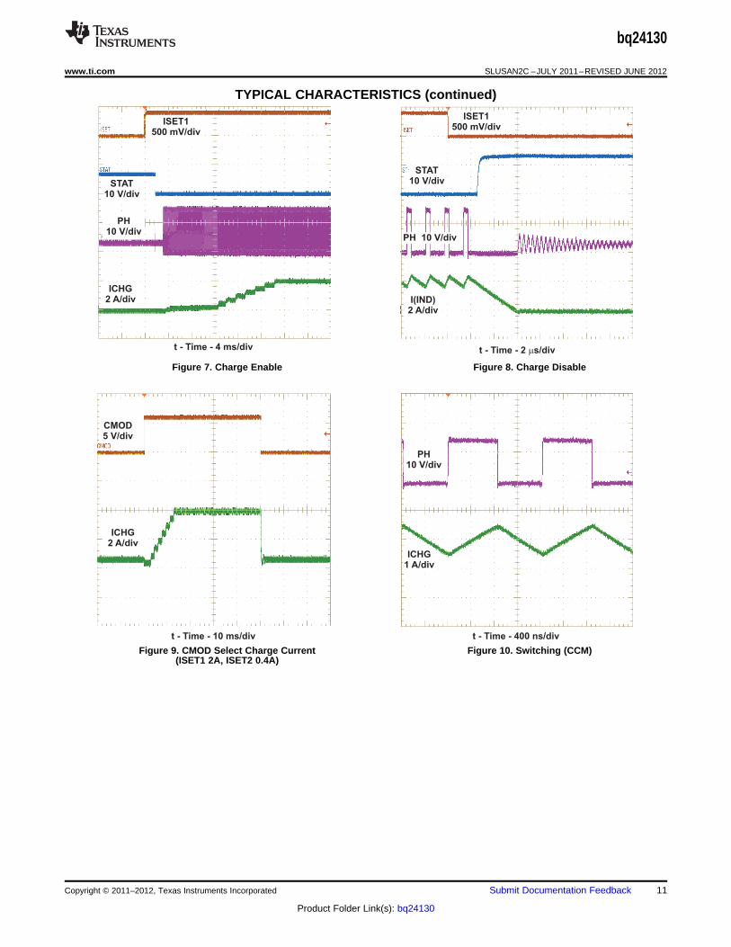
TYPICAL CHARACTERISTICS (continued)
Figure 7. Charge Enable Figure 8. Charge Disable
Figure 9. CMOD Select Charge Current Figure 10. Switching (CCM)(ISET1 2A, ISET2 0.4A)
Copyright © 2011–2012, Texas Instruments Incorporated Submit Documentation Feedback 11
Product Folder Link(s): bq24130
VBAT5 V/div
I(IND)2 A/div
PH 10 V/div
t - Time - 4 s/divm t - Time - 200 ms/div
AVCC
5 V/div
IOUT
1 A/div
PH 10 V/div
VCAP 5 V/div
t - Time - 400 ns/div
PH10 V/div
I(IND)500 mA/div
BAT5 V/div
t - Time - 400 ns/div
I(IND)2 A/div
PH 10 V/div
bq24130
SLUSAN2C –JULY 2011–REVISED JUNE 2012 www.ti.com
TYPICAL CHARACTERISTICS (continued)
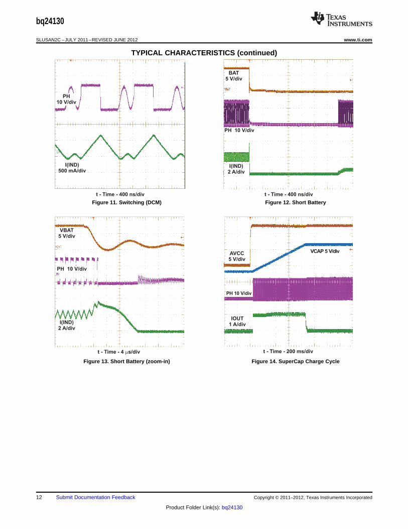
Figure 11. Switching (DCM) Figure 12. Short Battery
Figure 13. Short Battery (zoom-in) Figure 14. SuperCap Charge Cycle
12 Submit Documentation Feedback Copyright © 2011–2012, Texas Instruments Incorporated
Product Folder Link(s): bq24130
80
85
90
95
100
0 0.5 1 1.5 2 2.5 3 3.5 4
Eff
icie
nc
y -
%
Charge Current - A
V = 12 V
VBAT 3.6 VI
V = 12 V
VBAT 7.5 VI V = 5 V
VBAT 3.6 VI
bq24130
www.ti.com SLUSAN2C –JULY 2011–REVISED JUNE 2012
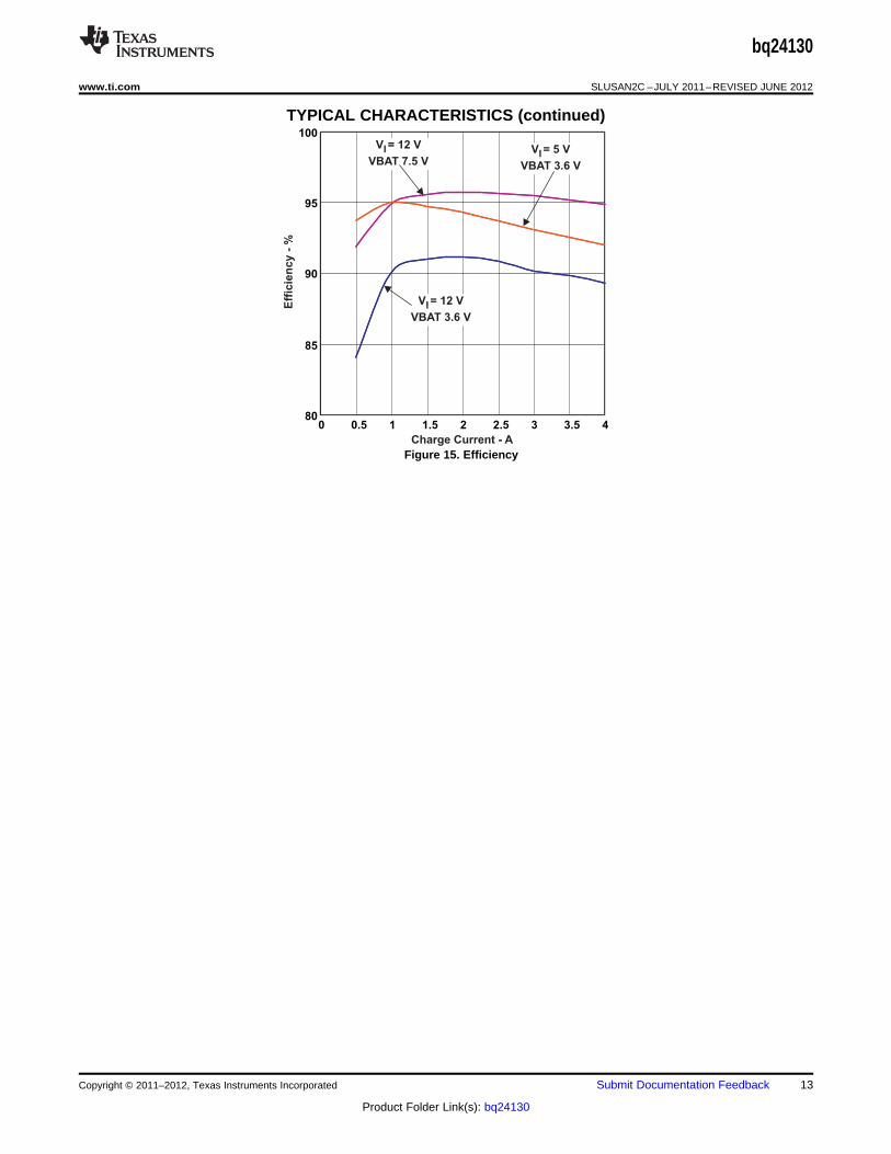
TYPICAL CHARACTERISTICS (continued)
Figure 15. Efficiency
Copyright © 2011–2012, Texas Instruments Incorporated Submit Documentation Feedback 13
Product Folder Link(s): bq24130
(ISET2)
(PRECHARGE)
(SR)
VI
100 R=
´
(ISET1)
(CHARGE)
(SR)
VI
20 R=
´
bq24130
SLUSAN2C –JULY 2011–REVISED JUNE 2012 www.ti.com
DETAILED DESCRIPTION
Battery Voltage Regulation
Internally, the BAT pin has 717 kΩ to AGND. For output voltage above 4.2 V, but not 8.4 V or 12 V, the user canuse an external resistor divider from output to VBAT pin to AGND.
The bq24130 offers a high accuracy voltage regulation on charge voltage. The bq24130 uses CELL pin to selectnumber of cells with a fixed 4.2 V/cell. CELL pin adjusts internal resistor voltage divider from BAT pin to AGNDpin for voltage feedback and regulate to internal 2.1 V voltage reference.
Table 1.
CELL Pin Voltage Regulation
AGND 4.2V
Floating 8.4V
VREF 12.6V
Internally, the BAT pin has 717 kΩ to AGND. For output voltage above 4.2 V, but not 8.4 V or 12 V, the user canuse an external resistor divider from output to the VBAT pin to AGND.
Battery Current Regulation
The bq24130 has two current setting inputs, ISET1 and ISET2.
A low-level signal on the CMOD pin forces the IC to charge at the pre-charge rate set on the ISET2 pin. A high-level signal forces charge at fast-charge rate as set by the ISET1 pin. The CMOD pin cannot float.
The ISET1 input sets the maximum charging current. Battery current is sensed by current sensing resistor RSRconnected between SRP and SRN. The full-scale differential voltage between SRP and SRN is 40 mV max. Theequation for charge current is:
(1)
The valid input voltage range of ISET1 is up to 0.8 V. With 10 mΩ sense resistor, the maximum output current is4 A. With 20 mΩ sense resistor, the maximum output current is 2 A.
The ISET2 input sets the pre-charge current up to 2 A on a 10 mΩ sense resistor.
(2)
The charger is disabled when ISET1 pin voltage is below 40 mV and is enabled when ISET1 pin voltage is above120 mV. For 10 mΩ current sensing resistor, the minimum fast charge current must higher than 600 mA.
Under high ambient temperature, the charge current will fold back to keep IC temperature not exceeding 120°C
Power Up
The charger uses a SLEEP comparator to determine the source of power on the AVCC pin, since AVCC can besupplied either from the battery or the adapter. If the AVCC voltage is greater than the SRN voltage, chargerexits SLEEP mode. If all conditions are met for charging, charger will then attempt to charge the battery (See theEnable and Disable Charging section). If the SRN voltage is greater than AVCC, charger enters a low quiescentcurrent 15 µA) SLEEP mode to minimize current drain from the battery. During the SLEEP mode, the VREFoutput turns off and the STAT pin goes to high impedance.
If AVCC is below the UVLO threshold, the device is disabled.
14 Submit Documentation Feedback Copyright © 2011–2012, Texas Instruments Incorporated
Product Folder Link(s): bq24130
bq24130
www.ti.com SLUSAN2C –JULY 2011–REVISED JUNE 2012
Enable and Disable Charging
The following conditions have to be valid before charge is enabled:• ISET1 pin above 120 mV• The device is not in Under Voltage Lockout (UVLO) mode (i.e. V(AVCC) > UVLO)• The device is not in SLEEP mode (i.e. V(AVCC) > V(SRN))• The AVCC voltage is lower than the AC over-voltage threshold (i.e. V(AVCC) < V(ACOV))• 50 ms delay is complete after initial power-up• The REGN and VREF LDO voltages are at the correct levels• Thermal Shut down (TSHUT) is not valid• No TS fault is detected
One of the following conditions will stop on-going charging:• ISET1 pin voltage is below 40mV;• The device is in UVLO mode;• Adapter is removed, causing the device to enter SLEEP mode;• AVCC voltage is over voltage• The REGN or VREF LDO voltage is overloaded;• TSHUT temperature threshold is reached.• TS voltage goes out of range indicating the battery temperature is too hot or too cold
Automatic Internal Soft-Start Charger Current
The charger automatically soft-starts the charger regulation current every time the charger goes into fast-chargeto ensure there is no overshoot or stress on the output capacitors or the power converter. The soft-start consistsof stepping-up the charge regulation current into 8 evenly divided steps up to the programmed charge current.Each step lasts around 1.6 ms, for a typical rise time of 12.8 ms. No external components are needed for thisfunction.
Converter Operation
The bq24130 employs a 600kHz constant-frequency step-down switching regulator. The fixed frequencyoscillator keeps tight control of the switching frequency under all conditions of input voltage, battery voltage,charge current and temperature, simplifying output filter design and keeping it out of the audible noise region.
A type III compensation network allows using ceramic capacitors at the output of the converter. An internal saw-tooth ramp is compared to the internal error control signals to vary the duty-cycle of the converter. The rampheight is proportional to the AVCC voltage to cancel out any loop gain variation due to a change in input voltage,and simplifies loop compensation. Internal gate drive logic allows achieving 97% duty cycle before pulse skippingstarts.
Charge Undercurrent Protection
When the voltage between BTST and SW falls below 4 V, the low-side FET turns on to provide refresh chargeup the bootstrap capacitor. After the recharge, if the SRP-SRN voltage decreases below 5 mV, the low side FETwill be turned off for the remainder of the switching cycle (i.e. non-synchronous operation). This is important toprevent negative inductor current from causing any boost effect in which the input voltage increases as power istransferred from the battery to the input capacitors. This can lead to an overvoltage on the AVCC node andpotentially cause damage to the system.
When the IC senses SRP-SRN average voltage drops below 1.25 mV (0.125 A of inductor current for a 10 mΩsense resistor) or the battery voltage is less than 2 V, the charger will enter non-synchronous mode and the low-side n-channel power MOSFET will stay off and rely on the body diode to make converter as a standard buck.This prevents the battery discharge current when battery is almost fully charged and current tapers down to alower level. The low-side n-channel power MOSFET will turn on when a bootstrap capacitor refresh pulse isneeded.
Copyright © 2011–2012, Texas Instruments Incorporated Submit Documentation Feedback 15
Product Folder Link(s): bq24130
bq24130
SLUSAN2C –JULY 2011–REVISED JUNE 2012 www.ti.com
Charge Overcurrent Protection
The charger monitors top side MOSFET current by high side sense FET. When peak current is higher than over-current threshold, it will turn off the top side MOSFET and keep it off until the next cycle. The charger has asecondary cycle-to-cycle over-current protection. It monitors the charge current, and prevents the current fromexceeding 160% of the programmed charge current. The high-side gate drive turns off when the overcurrent isdetected, and automatically resumes when the current falls below the over-current threshold.
Battery Overvoltage Protection
The converter will not allow the high-side FET to turn-on until the battery voltage goes below 102% of theregulation voltage. This allows one-cycle response to an over-voltage condition – such as occurs when the loadis removed or the battery is disconnected. An 8 mA current sink from SRP/SRN to AGND is on only duringcharge and allows discharging the stored output inductor energy that is transferred to the output capacitors. Ifbattery overvoltage condition lasts for more than 30 ms, charge is disabled.
Battery Short Protection
When SRN pin voltage is lower than 2 V it is considered as battery short condition during charging period. Thecharger will shut down immediately, then soft start back to the charging current 1.25 A max. This prevents highcurrent may build in output inductor and cause inductor saturation when battery terminal is shorted duringcharging. The converter works in non-synchronous mode during battery short.
Input Overvoltage Protection (ACOV)
ACOV provides protection to prevent system damage due to high input voltage. In bq24130, once the voltage onAVCC reaches the 18 V ACOV threshold, charge is disabled.
Input Under Voltage Lock Out (UVLO)
The system must have a minimum 3.85 V AVCC voltage to allow proper operation. This AVCC voltage couldcome from either input adapter or battery, since a conduction path exists from the battery to AVCC through thehigh side NMOS body diode. When AVCC is below the 3.85 V UVLO threshold, all circuits on the IC aredisabled.
Thermal Regulation and Shutdown Protection
The QFN package has low thermal impedance, which provides good thermal conduction from the silicon to theambient, to keep junctions temperatures low. The internal thermal regulation loop will adjust the charge current tomaintain the junction temperature around 120°C.
As added level of protection, the charger converter turns off and self-protects whenever the junction temperatureexceeds the TSHUT threshold of 150°C. The charger stays off until the junction temperature falls below 130°C.
Temperature Qualification
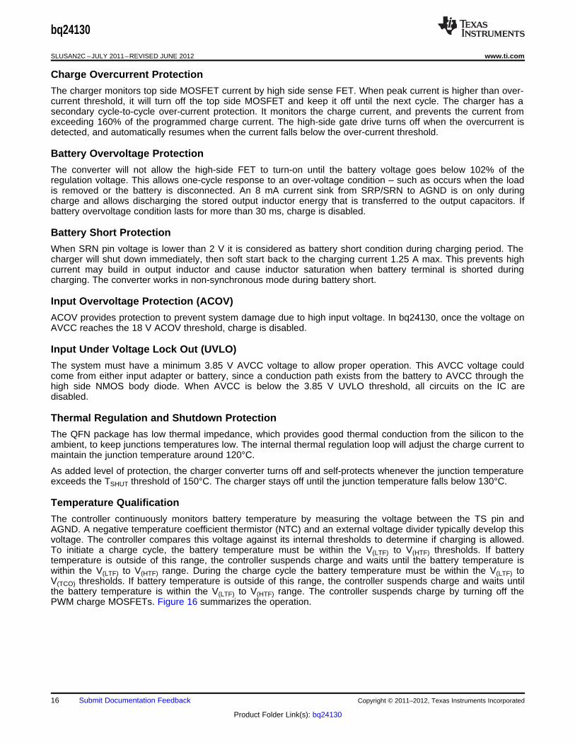
The controller continuously monitors battery temperature by measuring the voltage between the TS pin andAGND. A negative temperature coefficient thermistor (NTC) and an external voltage divider typically develop thisvoltage. The controller compares this voltage against its internal thresholds to determine if charging is allowed.To initiate a charge cycle, the battery temperature must be within the V(LTF) to V(HTF) thresholds. If batterytemperature is outside of this range, the controller suspends charge and waits until the battery temperature iswithin the V(LTF) to V(HTF) range. During the charge cycle the battery temperature must be within the V(LTF) toV(TCO) thresholds. If battery temperature is outside of this range, the controller suspends charge and waits untilthe battery temperature is within the V(LTF) to V(HTF) range. The controller suspends charge by turning off thePWM charge MOSFETs. Figure 16 summarizes the operation.
16 Submit Documentation Feedback Copyright © 2011–2012, Texas Instruments Incorporated
Product Folder Link(s): bq24130
(VREF)
(LTF)
(COLD)
V1
VRT1
1 1
RT2 RTH
-
=
+
(VREF) (COLD) (HOT)
(LTF) (TCO)
(VREF) (VREF)
(HOT) (COLD)
(TCO) (LTF)
1 1V RTH RTH
V VRT2
V VRTH 1 RTH 1
V V
æ ö÷ç ÷ç´ ´ ´ - ÷ç ÷÷çè ø=
æ ö æ ö÷ ÷ç ç÷ ÷ç ç´ - - ´ -÷ ÷ç ç÷ ÷÷ ÷ç çè ø è ø
TEMPERATURE RANGE
TO INITIATE CHARGE
TEMPERATURE RANGE
DURING A CHARGE CYCLE
CHARGE SUSPENDED CHARGE SUSPENDED
VREF VREF
CHARGE at full C CHARGE at full C
CHARGE SUSPENDEDCHARGE SUSPENDED
AGND AGND
V(LTF)
V(TCO)
V(LTFH)
V(LTF)
V(HTF)
V(LTFH)
bq24130
www.ti.com SLUSAN2C –JULY 2011–REVISED JUNE 2012
Figure 16. TS pin, Thermistor Sense Thresholds
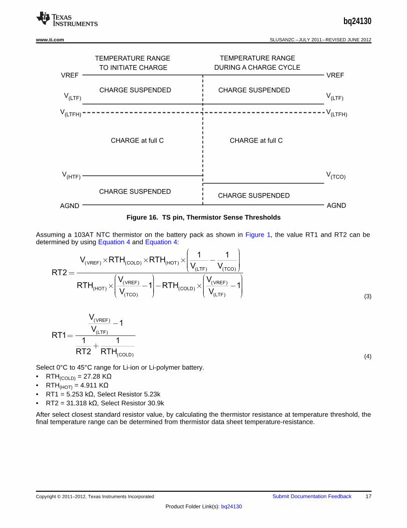
Assuming a 103AT NTC thermistor on the battery pack as shown in Figure 1, the value RT1 and RT2 can bedetermined by using Equation 4 and Equation 4:
(3)
SPACER
(4)
Select 0°C to 45°C range for Li-ion or Li-polymer battery.• RTH(COLD) = 27.28 KΩ• RTH(HOT) = 4.911 KΩ• RT1 = 5.253 kΩ, Select Resistor 5.23k• RT2 = 31.318 kΩ, Select Resistor 30.9k
After select closest standard resistor value, by calculating the thermistor resistance at temperature threshold, thefinal temperature range can be determined from thermistor data sheet temperature-resistance.
Copyright © 2011–2012, Texas Instruments Incorporated Submit Documentation Feedback 17
Product Folder Link(s): bq24130
o
1
2 LC=
p
f
VREF
TS
RT2
RT1
RTH
103AT
bq24130
bq24130
SLUSAN2C –JULY 2011–REVISED JUNE 2012 www.ti.com
Figure 17. TS Resistor Network
Inductor, Capacitor, and Sense Resistor Selection Guidelines
The IC provides internal loop compensation. With this scheme, best stability occurs when the LC resonantfrequency, fo, is approximately 12 kHz – 17 kHz for IC per Equation 5:
(5)
Charge Status Outputs
The open-drain STAT outputs indicate various charger operations as shown in . These status pins can be usedto drive LED or communicate with the host processor. Note that OFF indicates that the open-drain transistor isturned off.
Table 2. STAT Pin Defination
Charge State STAT
Charge in progress On
Sleep mode, Charge Disabled OFF
Chagre suspended. Input overvoltage, Battery overvoltage BLINK
18 Submit Documentation Feedback Copyright © 2011–2012, Texas Instruments Incorporated
Product Folder Link(s): bq24130
OUT OUT
O 2
IN
V VV 1
8LC s V
æ ö÷ç ÷D = -ç ÷ç ÷çè øf
(RIPPLE)
(COUT) (RIPPLE)
II 0.29 I
2 3= » ´
´
(CIN) (CHG)I I D (1 D)= ´ ´ -
IN(RIPPLE)
V D (1 D)I
s L
´ ´ -
=
´f
bq24130
www.ti.com SLUSAN2C –JULY 2011–REVISED JUNE 2012
APPLICATION INFORMATION
Inductor Selection
The bq24130 has 600 kHz switching frequency to allow the use of small inductor and capacitor values. TheInductor saturation current should be higher than the charging current (I(CHG)) plus half the ripple current(I(RIPPLE)):
I(SAT) ≥ I(CHG) + (1/2) I(RIPPLE) (6)
The inductor ripple current depends on input voltage (VIN), duty cycle (D = VOUT/VIN), switching frequency (fs)and inductance (L):
(7)
Input Capacitor
Input capacitor should have enough ripple current rating to absorb input switching ripple current. The worst caseRMS ripple current is half of the charging current when duty cycle is 0.5. If the converter does not operate at50% duty cycle, then the worst case capacitor RMS current I(CIN) occurs where the duty cycle is closest to 50%and can be estimated by Equation 8:
(8)
Low ESR ceramic capacitor such as X7R or X5R is preferred for input decoupling capacitor and should beplaced to the drain of the high side MOSFET and source of the low side MOSFET as close as possible. Voltagerating of the capacitor must be higher than normal input voltage level. 25 V rating or higher capacitor is preferredfor 15 V input voltage. 20 μF capacitance is suggested for typical of 3 A - 4 A charging current.
Output Capacitor
Output capacitor also should have enough ripple current rating to absorb output switching ripple current. Theoutput capacitor RMS current I(COUT) is given:
(9)
The output capacitor voltage ripple can be calculated as follows:
(10)
At certain input/output voltage and switching frequency, the voltage ripple can be reduced by increasing theoutput filter LC.
The bq24130 has internal loop compensator. To get good loop stability, the resonant frequency of the outputinductor and output capacitor should be designed between 12 kHz and 17 kHz. The preferred ceramic capacitoris 25 V or higher rating, X7R or X5R
Input Filter Design
During adapter hot plug-in, the parasitic inductance and input capacitor from the adapter cable form a secondorder system. The voltage spike at AVCC/PVCC pin may be beyond IC maximum voltage rating and damage IC.The input filter must be carefully designed and tested to prevent overvoltage event on AVCC/PVCC pin.
There are several methods to damping or limit the overvoltage spike during adapter hot plug-in. An electrolyticcapacitor with high ESR as an input capacitor can damp the overvoltage spike well below the IC maximum pinvoltage rating. A high current capability TVS Zener diode can also limit the over voltage level to an IC safe level.However, these two solutions may not have low cost or small size.
Copyright © 2011–2012, Texas Instruments Incorporated Submit Documentation Feedback 19
Product Folder Link(s): bq24130
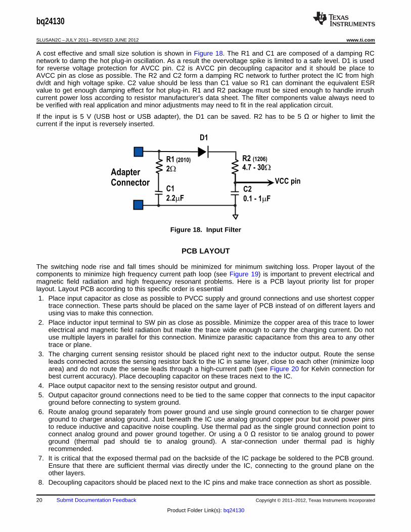
C1
2.2 Fm
AdapterConnector
R1 (2010)
2W
D1
C2
0.1 - 1 Fm
R2 (1206)
4.7 - 30W
VCC pin
bq24130
SLUSAN2C –JULY 2011–REVISED JUNE 2012 www.ti.com
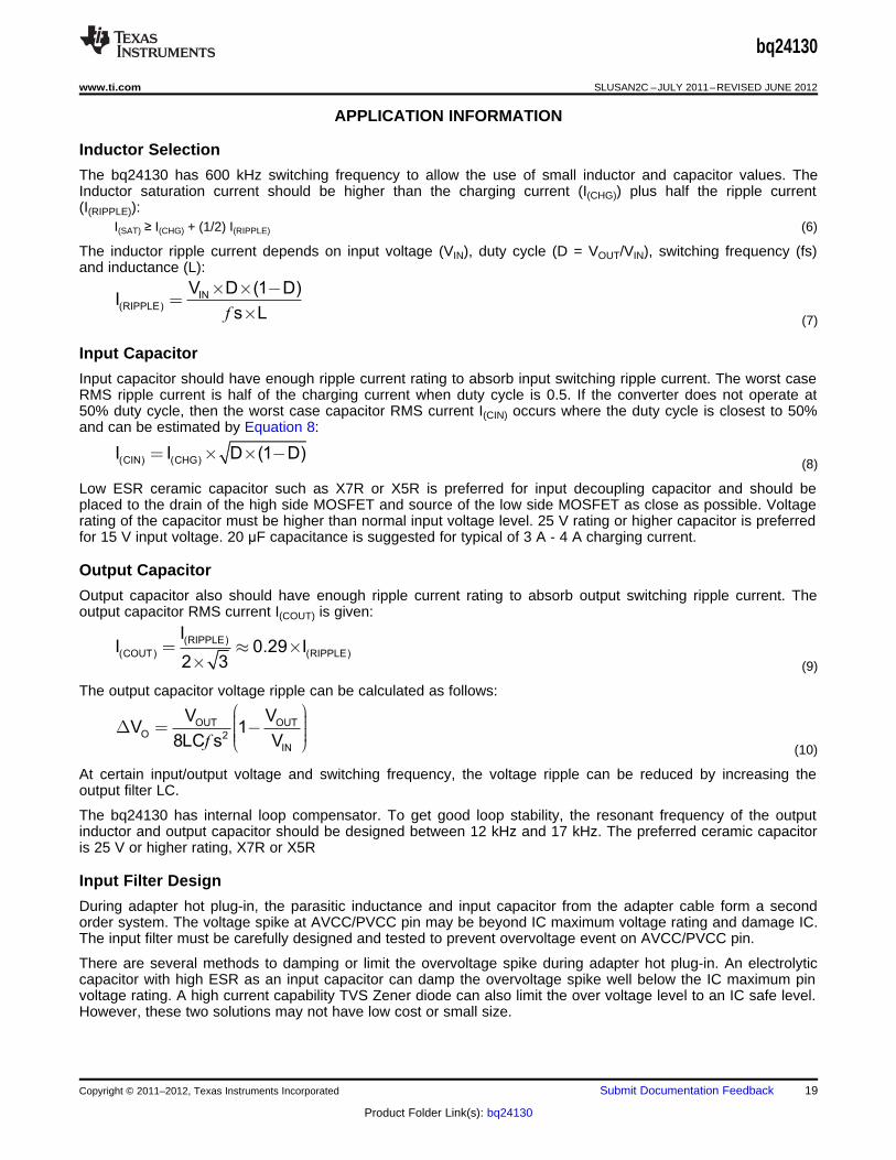
A cost effective and small size solution is shown in Figure 18. The R1 and C1 are composed of a damping RCnetwork to damp the hot plug-in oscillation. As a result the overvoltage spike is limited to a safe level. D1 is usedfor reverse voltage protection for AVCC pin. C2 is AVCC pin decoupling capacitor and it should be place toAVCC pin as close as possible. The R2 and C2 form a damping RC network to further protect the IC from highdv/dt and high voltage spike. C2 value should be less than C1 value so R1 can dominant the equivalent ESRvalue to get enough damping effect for hot plug-in. R1 and R2 package must be sized enough to handle inrushcurrent power loss according to resistor manufacturer’s data sheet. The filter components value always need tobe verified with real application and minor adjustments may need to fit in the real application circuit.
If the input is 5 V (USB host or USB adapter), the D1 can be saved. R2 has to be 5 Ω or higher to limit thecurrent if the input is reversely inserted.
Figure 18. Input Filter
PCB LAYOUT
The switching node rise and fall times should be minimized for minimum switching loss. Proper layout of thecomponents to minimize high frequency current path loop (see Figure 19) is important to prevent electrical andmagnetic field radiation and high frequency resonant problems. Here is a PCB layout priority list for properlayout. Layout PCB according to this specific order is essential1. Place input capacitor as close as possible to PVCC supply and ground connections and use shortest copper
trace connection. These parts should be placed on the same layer of PCB instead of on different layers andusing vias to make this connection.
2. Place inductor input terminal to SW pin as close as possible. Minimize the copper area of this trace to lowerelectrical and magnetic field radiation but make the trace wide enough to carry the charging current. Do notuse multiple layers in parallel for this connection. Minimize parasitic capacitance from this area to any othertrace or plane.
3. The charging current sensing resistor should be placed right next to the inductor output. Route the senseleads connected across the sensing resistor back to the IC in same layer, close to each other (minimize looparea) and do not route the sense leads through a high-current path (see Figure 20 for Kelvin connection forbest current accuracy). Place decoupling capacitor on these traces next to the IC.
4. Place output capacitor next to the sensing resistor output and ground.5. Output capacitor ground connections need to be tied to the same copper that connects to the input capacitor
ground before connecting to system ground.6. Route analog ground separately from power ground and use single ground connection to tie charger power
ground to charger analog ground. Just beneath the IC use analog ground copper pour but avoid power pinsto reduce inductive and capacitive noise coupling. Use thermal pad as the single ground connection point toconnect analog ground and power ground together. Or using a 0 Ω resistor to tie analog ground to powerground (thermal pad should tie to analog ground). A star-connection under thermal pad is highlyrecommended.
7. It is critical that the exposed thermal pad on the backside of the IC package be soldered to the PCB ground.Ensure that there are sufficient thermal vias directly under the IC, connecting to the ground plane on theother layers.
8. Decoupling capacitors should be placed next to the IC pins and make trace connection as short as possible.
20 Submit Documentation Feedback Copyright © 2011–2012, Texas Instruments Incorporated
Product Folder Link(s): bq24130
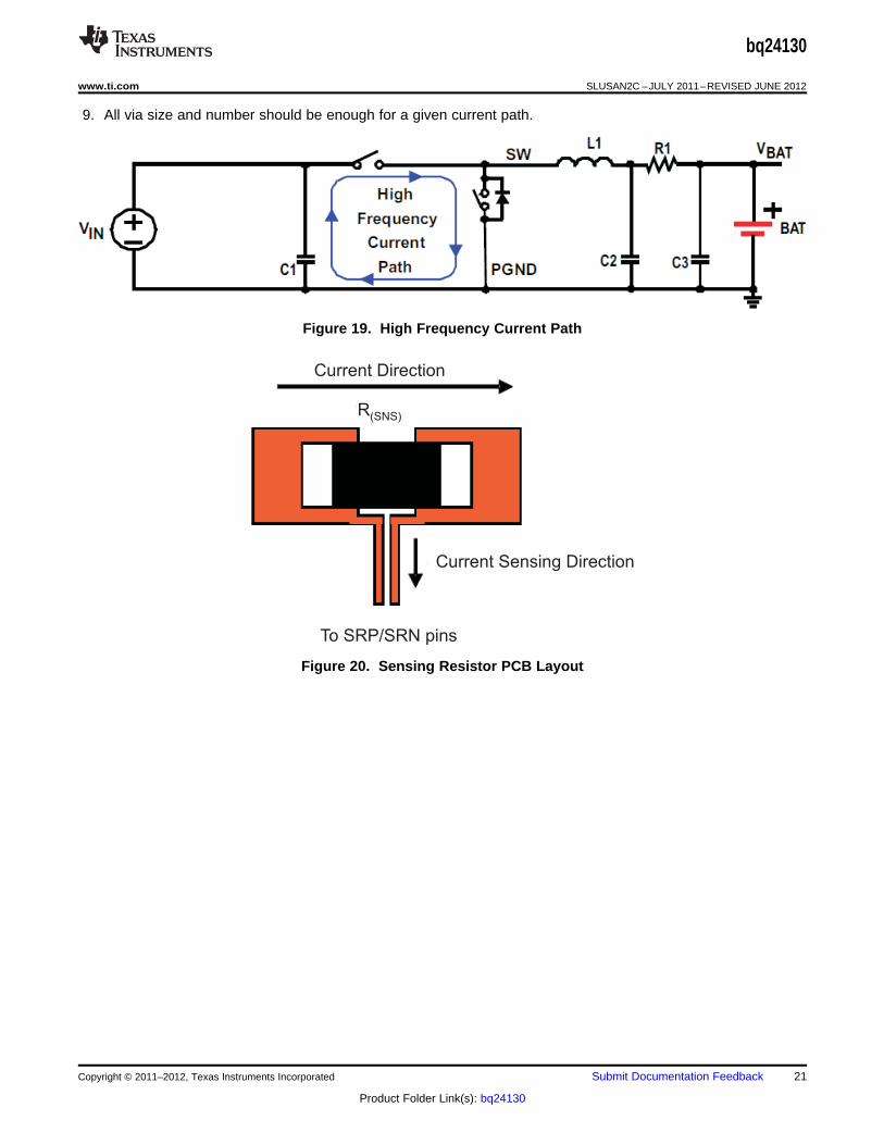
To SRP/SRN pins
Current Sensing Direction
Current Direction
R(SNS)
bq24130
www.ti.com SLUSAN2C –JULY 2011–REVISED JUNE 2012
9. All via size and number should be enough for a given current path.
Figure 19. High Frequency Current Path
Figure 20. Sensing Resistor PCB Layout
Copyright © 2011–2012, Texas Instruments Incorporated Submit Documentation Feedback 21
Product Folder Link(s): bq24130
bq24130
SLUSAN2C –JULY 2011–REVISED JUNE 2012 www.ti.com
REVISION HISTORY
Changes from Original (July 2011) to Revision A Page
• Added the Li-Ion/Li-Polymer battery Application ................................................................................................................... 1
• Changed pin BTST Description From: Connect the 0.1 µF bootstrap capacitor. To: Connect the 47 nF bootstrapcapacitor ............................................................................................................................................................................... 2
• Changed the Min and Max values for Voltage in the ABS Max Ratings Table .................................................................... 3
• Changed the RECOMMENDED OPERATING CONDITIONS table .................................................................................... 3
• Changed the ELECT CHARACTERISTICS conditions statement From: 4.5 V ≤ V(PVCC, AVCC) ≤ 18 V To: 4.5 V ≤V(PVCC, AVCC) ≤ 17 V ............................................................................................................................................................... 4
• Changed the Electrical Characteristics table ........................................................................................................................ 4
• Added Figure 2 ..................................................................................................................................................................... 9
• Added the TYPICAL CHARACTERISTICS section ............................................................................................................ 10
• Changed the Battery Voltage Regulation section ............................................................................................................... 14
• Changed the Charge Overcurrent Protection section ......................................................................................................... 16
Changes from Revision A (August 2011) to Revision B Page
• Added Features Bullet: Constant Current Super Capacitor Charging .................................................................................. 1
• Changed the Thermal Information Table .............................................................................................................................. 3
• Changed Figure 1 ................................................................................................................................................................. 8
• Changed Figure 2 ................................................................................................................................................................. 9
• Changed Figure 14 ............................................................................................................................................................. 12
Changes from Revision B (August 2011) to Revision C Page
• Changed the value of RT1 From: RT1 = 31.23 KΩ To: RT1 = 5.253 kΩ, Select Resistor 5.23k ....................................... 17
• Changed the value of RT2 From: RT2 = 5.25 KΩ To: RT2 = 31.318 kΩ, Select Resistor 30.9k ....................................... 17
22 Submit Documentation Feedback Copyright © 2011–2012, Texas Instruments Incorporated
Product Folder Link(s): bq24130
PACKAGE OPTION ADDENDUM
www.ti.com 27-Jul-2013
Addendum-Page 1
PACKAGING INFORMATION
Orderable Device Status(1)
Package Type PackageDrawing
Pins PackageQty
Eco Plan(2)
Lead/Ball Finish MSL Peak Temp(3)
Op Temp (°C) Device Marking(4/5)
Samples
BQ24130RHLR ACTIVE VQFN RHL 20 3000 Green (RoHS& no Sb/Br)
CU NIPDAU Level-2-260C-1 YEAR -40 to 85 BQ24130
BQ24130RHLT ACTIVE VQFN RHL 20 250 Green (RoHS& no Sb/Br)
CU NIPDAU Level-2-260C-1 YEAR -40 to 85 BQ24130
(1) The marketing status values are defined as follows:ACTIVE: Product device recommended for new designs.LIFEBUY: TI has announced that the device will be discontinued, and a lifetime-buy period is in effect.NRND: Not recommended for new designs. Device is in production to support existing customers, but TI does not recommend using this part in a new design.PREVIEW: Device has been announced but is not in production. Samples may or may not be available.OBSOLETE: TI has discontinued the production of the device.
(2) Eco Plan - The planned eco-friendly classification: Pb-Free (RoHS), Pb-Free (RoHS Exempt), or Green (RoHS & no Sb/Br) - please check http://www.ti.com/productcontent for the latest availabilityinformation and additional product content details.TBD: The Pb-Free/Green conversion plan has not been defined.Pb-Free (RoHS): TI's terms "Lead-Free" or "Pb-Free" mean semiconductor products that are compatible with the current RoHS requirements for all 6 substances, including the requirement thatlead not exceed 0.1% by weight in homogeneous materials. Where designed to be soldered at high temperatures, TI Pb-Free products are suitable for use in specified lead-free processes.Pb-Free (RoHS Exempt): This component has a RoHS exemption for either 1) lead-based flip-chip solder bumps used between the die and package, or 2) lead-based die adhesive used betweenthe die and leadframe. The component is otherwise considered Pb-Free (RoHS compatible) as defined above.Green (RoHS & no Sb/Br): TI defines "Green" to mean Pb-Free (RoHS compatible), and free of Bromine (Br) and Antimony (Sb) based flame retardants (Br or Sb do not exceed 0.1% by weightin homogeneous material)
(3) MSL, Peak Temp. -- The Moisture Sensitivity Level rating according to the JEDEC industry standard classifications, and peak solder temperature.
(4) There may be additional marking, which relates to the logo, the lot trace code information, or the environmental category on the device.
(5) Multiple Device Markings will be inside parentheses. Only one Device Marking contained in parentheses and separated by a "~" will appear on a device. If a line is indented then it is a continuationof the previous line and the two combined represent the entire Device Marking for that device.
Important Information and Disclaimer:The information provided on this page represents TI's knowledge and belief as of the date that it is provided. TI bases its knowledge and belief on informationprovided by third parties, and makes no representation or warranty as to the accuracy of such information. Efforts are underway to better integrate information from third parties. TI has taken andcontinues to take reasonable steps to provide representative and accurate information but may not have conducted destructive testing or chemical analysis on incoming materials and chemicals.TI and TI suppliers consider certain information to be proprietary, and thus CAS numbers and other limited information may not be available for release.
In no event shall TI's liability arising out of such information exceed the total purchase price of the TI part(s) at issue in this document sold by TI to Customer on an annual basis.
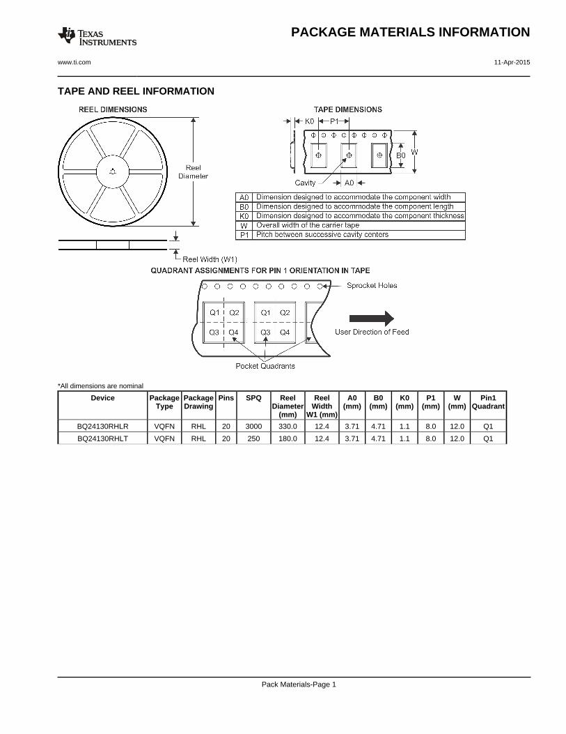
TAPE AND REEL INFORMATION
*All dimensions are nominal
Device PackageType
PackageDrawing
Pins SPQ ReelDiameter
(mm)
ReelWidth
W1 (mm)
A0(mm)
B0(mm)
K0(mm)
P1(mm)
W(mm)
Pin1Quadrant
BQ24130RHLR VQFN RHL 20 3000 330.0 12.4 3.71 4.71 1.1 8.0 12.0 Q1
BQ24130RHLT VQFN RHL 20 250 180.0 12.4 3.71 4.71 1.1 8.0 12.0 Q1
PACKAGE MATERIALS INFORMATION
www.ti.com 11-Apr-2015
Pack Materials-Page 1

*All dimensions are nominal
Device Package Type Package Drawing Pins SPQ Length (mm) Width (mm) Height (mm)
BQ24130RHLR VQFN RHL 20 3000 367.0 367.0 35.0
BQ24130RHLT VQFN RHL 20 250 210.0 185.0 35.0
PACKAGE MATERIALS INFORMATION
www.ti.com 11-Apr-2015
Pack Materials-Page 2
NOTES:
1. All linear dimensions are in millimeters. Any dimensions in parenthesis are for reference only. Dimensioning and tolerancingper ASME Y14.5M.
2. This drawing is subject to change without notice.3. The package thermal pad must be soldered to the printed circuit board for thermal and mechanical performance.
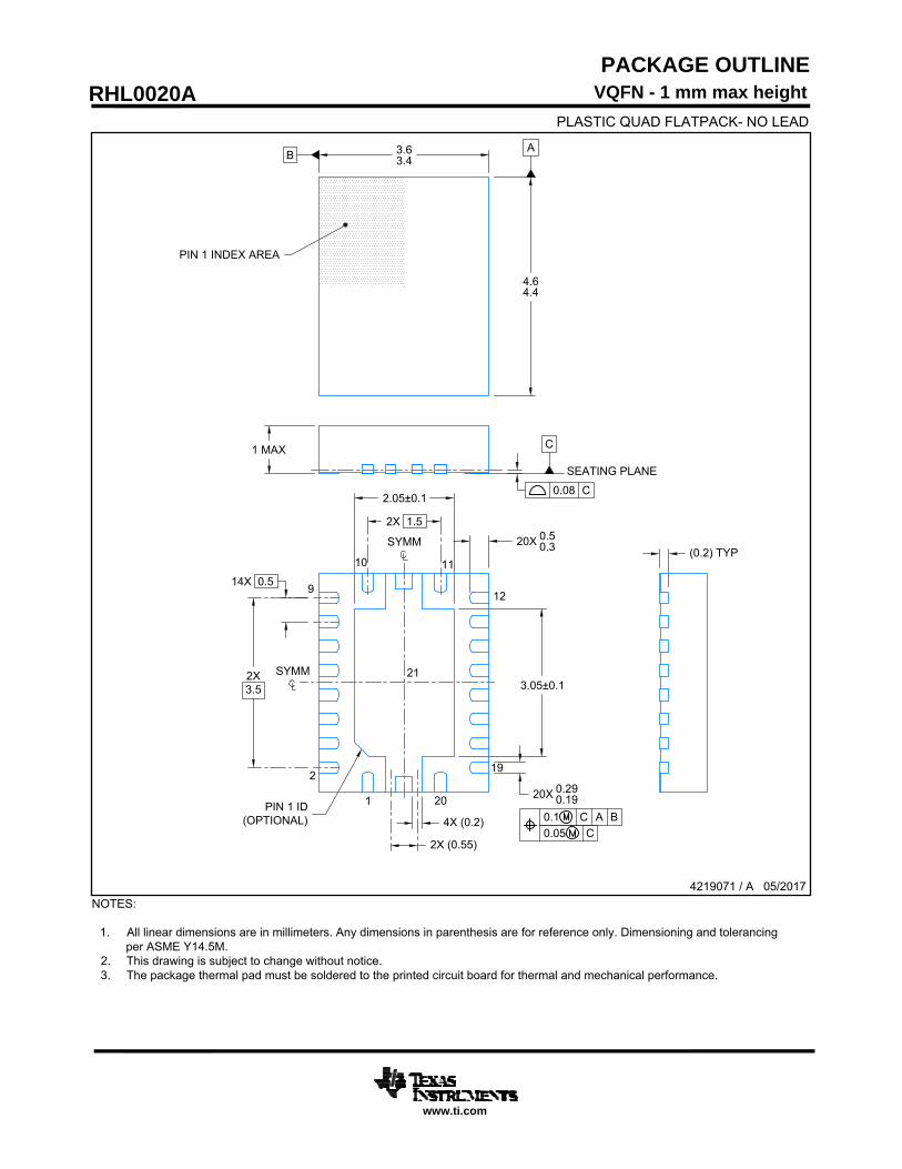
PACKAGE OUTLINE
4219071 / A 05/2017
www.ti.com
VQFN - 1 mm max height
PLASTIC QUAD FLATPACK- NO LEAD
RHL0020A
A
0.08 C
0.1 C A B0.05 C
B
SYMM
SYMM
PIN 1 INDEX AREA
SEATING PLANE
C
1PIN 1 ID(OPTIONAL)
2.05±0.1
3.05±0.1
3.63.4
4.64.4
1 MAX
(0.2) TYP
2X (0.55)
2X3.5
14X 0.5
2
9
10 11
12
19
20
2X 1.5
4X (0.2)
20X 0.290.19
20X 0.50.3
21
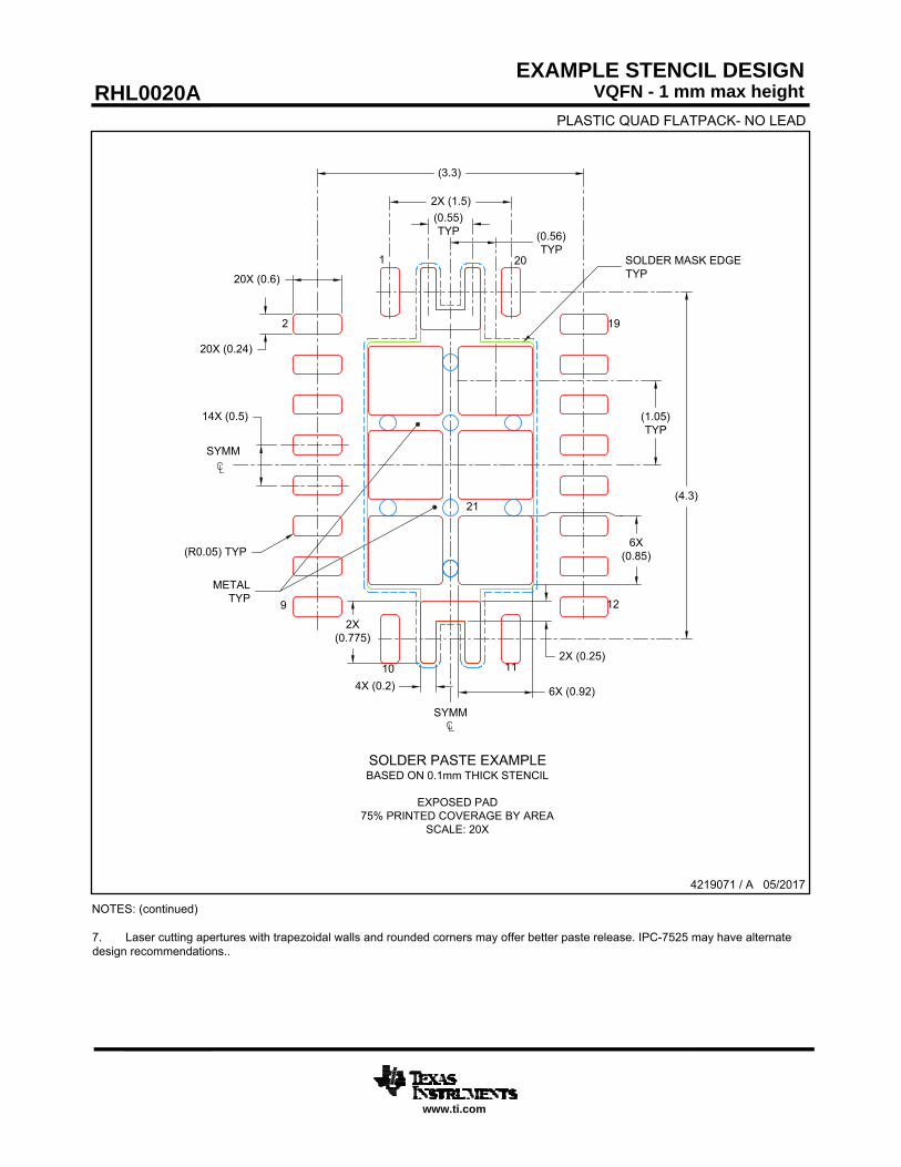
NOTES: (continued)
4. This package is designed to be soldered to a thermal pad on the board. For more information, see Texas Instrumentsliterature number SLUA271 (www.ti.com/lit/slua271) .
5. Solder mask tolerances between and around signal pads can vary based on board fabrication site.6. Vias are optional depending on application, refer to device data sheet. If any vias are implemented, refer to theri
locations shown on this view. It is recommended that vias under paste be filled, plugged or tented.
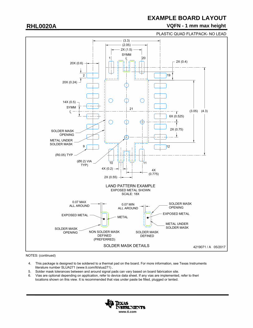
EXAMPLE BOARD LAYOUT
4219071 / A 05/2017
www.ti.com
VQFN - 1 mm max height
RHL0020A
PLASTIC QUAD FLATPACK- NO LEAD
SYMM
SYMM
LAND PATTERN EXAMPLEEXPOSED METAL SHOWN
SCALE: 18X
2X (1.5)
6X (0.525)
4X(0.775)
(4.3)
(3.3)
20X (0.6)
20X (0.24)
14X (0.5)
(3.05)
(2.05)
(R0.05) TYP
(Ø0.2) VIATYP)
1
2
9
10 11
12
19
20
0.07 MAXALL AROUND 0.07 MIN
ALL AROUND
SOLDER MASK DETAILS
NON SOLDER MASKDEFINED
(PREFERRED)
SOLDER MASKDEFINED
METAL
SOLDER MASKOPENING
SOLDER MASKOPENING
METAL UNDERSOLDER MASK
21
2X (0.75)
2X (0.4)
SOLDER MASKOPENING
METAL UNDERSOLDER MASK
4X (0.2)
2X (0.55)
EXPOSED METAL EXPOSED METAL
NOTES: (continued)
7. Laser cutting apertures with trapezoidal walls and rounded corners may offer better paste release. IPC-7525 may have alternatedesign recommendations..
EXAMPLE STENCIL DESIGN
4219071 / A 05/2017
www.ti.com
VQFN - 1 mm max height
RHL0020A
PLASTIC QUAD FLATPACK- NO LEAD
SYMM
SYMM
SOLDER PASTE EXAMPLEBASED ON 0.1mm THICK STENCIL
EXPOSED PAD75% PRINTED COVERAGE BY AREA
SCALE: 20X
(4.3)
2X (1.5)
(3.3)
(1.05)TYP
6X (0.92)
6X(0.85)
14X (0.5)
20X (0.24)
20X (0.6)
(0.56)TYP
METALTYP
21
4X (0.2)
2X (0.25)
(0.55)TYP
SOLDER MASK EDGETYP
2X(0.775)
1
2
9
10 11
12
19
20
(R0.05) TYP
IMPORTANT NOTICE
Texas Instruments Incorporated (TI) reserves the right to make corrections, enhancements, improvements and other changes to itssemiconductor products and services per JESD46, latest issue, and to discontinue any product or service per JESD48, latest issue. Buyersshould obtain the latest relevant information before placing orders and should verify that such information is current and complete.TI’s published terms of sale for semiconductor products (http://www.ti.com/sc/docs/stdterms.htm) apply to the sale of packaged integratedcircuit products that TI has qualified and released to market. Additional terms may apply to the use or sale of other types of TI products andservices.Reproduction of significant portions of TI information in TI data sheets is permissible only if reproduction is without alteration and isaccompanied by all associated warranties, conditions, limitations, and notices. TI is not responsible or liable for such reproduceddocumentation. Information of third parties may be subject to additional restrictions. Resale of TI products or services with statementsdifferent from or beyond the parameters stated by TI for that product or service voids all express and any implied warranties for theassociated TI product or service and is an unfair and deceptive business practice. TI is not responsible or liable for any such statements.Buyers and others who are developing systems that incorporate TI products (collectively, “Designers”) understand and agree that Designersremain responsible for using their independent analysis, evaluation and judgment in designing their applications and that Designers havefull and exclusive responsibility to assure the safety of Designers' applications and compliance of their applications (and of all TI productsused in or for Designers’ applications) with all applicable regulations, laws and other applicable requirements. Designer represents that, withrespect to their applications, Designer has all the necessary expertise to create and implement safeguards that (1) anticipate dangerousconsequences of failures, (2) monitor failures and their consequences, and (3) lessen the likelihood of failures that might cause harm andtake appropriate actions. Designer agrees that prior to using or distributing any applications that include TI products, Designer willthoroughly test such applications and the functionality of such TI products as used in such applications.TI’s provision of technical, application or other design advice, quality characterization, reliability data or other services or information,including, but not limited to, reference designs and materials relating to evaluation modules, (collectively, “TI Resources”) are intended toassist designers who are developing applications that incorporate TI products; by downloading, accessing or using TI Resources in anyway, Designer (individually or, if Designer is acting on behalf of a company, Designer’s company) agrees to use any particular TI Resourcesolely for this purpose and subject to the terms of this Notice.TI’s provision of TI Resources does not expand or otherwise alter TI’s applicable published warranties or warranty disclaimers for TIproducts, and no additional obligations or liabilities arise from TI providing such TI Resources. TI reserves the right to make corrections,enhancements, improvements and other changes to its TI Resources. TI has not conducted any testing other than that specificallydescribed in the published documentation for a particular TI Resource.Designer is authorized to use, copy and modify any individual TI Resource only in connection with the development of applications thatinclude the TI product(s) identified in such TI Resource. NO OTHER LICENSE, EXPRESS OR IMPLIED, BY ESTOPPEL OR OTHERWISETO ANY OTHER TI INTELLECTUAL PROPERTY RIGHT, AND NO LICENSE TO ANY TECHNOLOGY OR INTELLECTUAL PROPERTYRIGHT OF TI OR ANY THIRD PARTY IS GRANTED HEREIN, including but not limited to any patent right, copyright, mask work right, orother intellectual property right relating to any combination, machine, or process in which TI products or services are used. Informationregarding or referencing third-party products or services does not constitute a license to use such products or services, or a warranty orendorsement thereof. Use of TI Resources may require a license from a third party under the patents or other intellectual property of thethird party, or a license from TI under the patents or other intellectual property of TI.TI RESOURCES ARE PROVIDED “AS IS” AND WITH ALL FAULTS. TI DISCLAIMS ALL OTHER WARRANTIES ORREPRESENTATIONS, EXPRESS OR IMPLIED, REGARDING RESOURCES OR USE THEREOF, INCLUDING BUT NOT LIMITED TOACCURACY OR COMPLETENESS, TITLE, ANY EPIDEMIC FAILURE WARRANTY AND ANY IMPLIED WARRANTIES OFMERCHANTABILITY, FITNESS FOR A PARTICULAR PURPOSE, AND NON-INFRINGEMENT OF ANY THIRD PARTY INTELLECTUALPROPERTY RIGHTS. TI SHALL NOT BE LIABLE FOR AND SHALL NOT DEFEND OR INDEMNIFY DESIGNER AGAINST ANY CLAIM,INCLUDING BUT NOT LIMITED TO ANY INFRINGEMENT CLAIM THAT RELATES TO OR IS BASED ON ANY COMBINATION OFPRODUCTS EVEN IF DESCRIBED IN TI RESOURCES OR OTHERWISE. IN NO EVENT SHALL TI BE LIABLE FOR ANY ACTUAL,DIRECT, SPECIAL, COLLATERAL, INDIRECT, PUNITIVE, INCIDENTAL, CONSEQUENTIAL OR EXEMPLARY DAMAGES INCONNECTION WITH OR ARISING OUT OF TI RESOURCES OR USE THEREOF, AND REGARDLESS OF WHETHER TI HAS BEENADVISED OF THE POSSIBILITY OF SUCH DAMAGES.Unless TI has explicitly designated an individual product as meeting the requirements of a particular industry standard (e.g., ISO/TS 16949and ISO 26262), TI is not responsible for any failure to meet such industry standard requirements.Where TI specifically promotes products as facilitating functional safety or as compliant with industry functional safety standards, suchproducts are intended to help enable customers to design and create their own applications that meet applicable functional safety standardsand requirements. Using products in an application does not by itself establish any safety features in the application. Designers mustensure compliance with safety-related requirements and standards applicable to their applications. Designer may not use any TI products inlife-critical medical equipment unless authorized officers of the parties have executed a special contract specifically governing such use.Life-critical medical equipment is medical equipment where failure of such equipment would cause serious bodily injury or death (e.g., lifesupport, pacemakers, defibrillators, heart pumps, neurostimulators, and implantables). Such equipment includes, without limitation, allmedical devices identified by the U.S. Food and Drug Administration as Class III devices and equivalent classifications outside the U.S.TI may expressly designate certain products as completing a particular qualification (e.g., Q100, Military Grade, or Enhanced Product).Designers agree that it has the necessary expertise to select the product with the appropriate qualification designation for their applicationsand that proper product selection is at Designers’ own risk. Designers are solely responsible for compliance with all legal and regulatoryrequirements in connection with such selection.Designer will fully indemnify TI and its representatives against any damages, costs, losses, and/or liabilities arising out of Designer’s non-compliance with the terms and provisions of this Notice.
Mailing Address: Texas Instruments, Post Office Box 655303, Dallas, Texas 75265Copyright © 2018, Texas Instruments Incorporated