Embed Size (px)
Citation preview
SKP5050SCANNING KELVIN PROBE SYSTEM
The Kelvin Probe is a non-contact, non-destructive vibrating capacitor device used to measure the work function (wf) of conducting materials or surface potential of semiconductor or insulating surfaces. The wf of a surface is typically defi ned by the topmost 1-3 layers of atoms or molecules, so the Kelvin Probe is one of the most sensitive surface analysis techniques available. KP Technology Systems off er very high wf resolution of 1-3 meV, currently the highest achieved by any commercial device.
KP Technology, The Kelvin Probe Specialists
KP Technology Ltd, Burn Street, Wick, Scotland, KW1 5EH. T:+44(0)1955 602777 F:+44(0)1955 602555 E:[email protected] www.kelvinprobe.com
Prof. Andrew AhnHarvard University, USA
I have been working the scanning Kelvin Probe and I
have become quite comfortable with it. It is an excellent device and exquisitely sensitive.
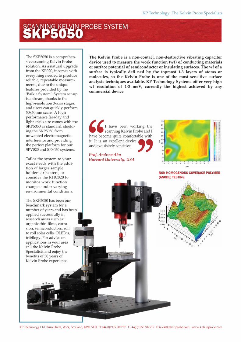
NON HOMOGENOUS COVERAGE POLYMER (ANODE) TESTING
The SKP5050 is a comprehen-sive scanning Kelvin Probe solution. As a natural upgrade from the KP020, it comes with everything needed to produce reliable, repeatable measure-ments, due to the unique features provided by the ‘Baikie System’. System set-up is a dream, thanks to the high-resolution 3-axis stages, and users can quickly perform 50x50mm scans. A high performance faraday and light enclosure comes with the SKP5050 as standard, shield-ing the SKP5050 from unwanted electromagnetic interference and providing the perfect platform for our SPV020 and SPS030 systems.
Tailor the system to your exact needs with the addi-tion of larger sample holders or heaters, or consider the RHC020 to monitor work function changes under varying environmental conditions.
The SKP5050 has been our benchmark system for a number of years and has been applied successfully in research areas such as: organic thin-films, corro-sion, semiconductors, roll to roll solar cells, OLED’s, tribilogy. For advice on applications in your area call the Kelvin Probe Specialists and enjoy the benefits of 30 years of Kelvin Probe experience.
KP Technology, The Kelvin Probe Specialists
KP Technology Ltd, Burn Street, Wick, Scotland, KW1 5EH. T:+44(0)1955 602777 F:+44(0)1955 602555 E:[email protected] www.kelvinprobe.com
THE BAIKIE SYSTEM
All KP Technology Systems are based upon unique features developed by Professor Iain Baikie. These features are unsurpassed by any other company.
u Highest work function/ surface potential resolution of 1 - 3 meV (standard with 2mm tip).
u Voice Coil driver provides very high rejection of driver talkover noise compared with piezoelectric systems.
u Off null signal detection system for vastly improved resolution - Our Signal-to-Noise (S/N) features remain unsurpassed in the field.
u Height regulation feature to control the tip to sample spacing during measure-ments and scans which allow for stable, reliable and repeatable results.
u Full digital control of all Kelvin Probe parameters.
SYSTEM SPECIFICATIONSu 2mm and 50 micron tips standardu Work Function resolution of 1-3meV (2mm tip), 5-10meV (50 micron with optical table support)u 50mm x 50 mm maximum scan areau 318 nanometer position resolutionu Tracking System with automatic motorized control of tip to sample spacingu Additional Manual Height Control (25.4mm KP translation for coarse positioning)u Off-null detection system with parasitic capacity rejection
SOFTWARE FEATURESu Digital Control of all Kelvin Probe parametersu Simple set-up procedure for signal optimisationu Fast measurement mode for tracking real time work function changes (1000 work function points / min at ~20meV resolution)u Variable scan size and real-time 3D charting of sample work functionu Export of data to scientific analysis software
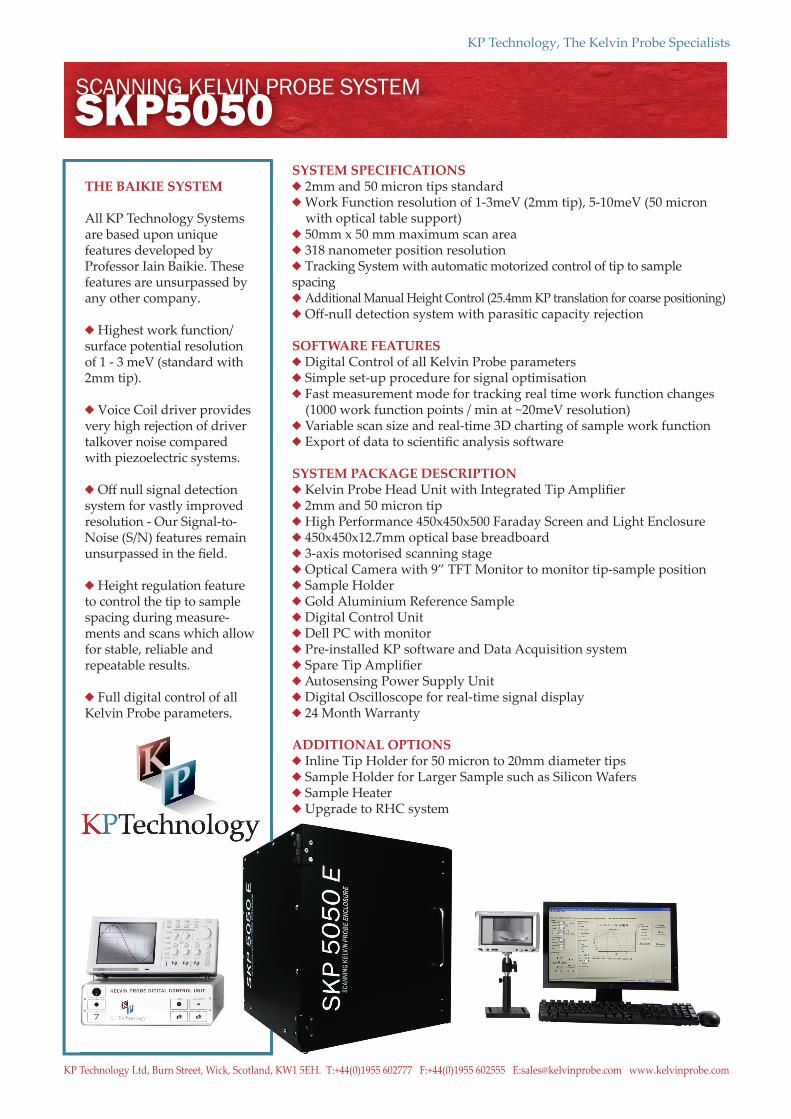
SYSTEM PACKAGE DESCRIPTIONu Kelvin Probe Head Unit with Integrated Tip Amplifieru 2mm and 50 micron tipu High Performance 450x450x500 Faraday Screen and Light Enclosureu 450x450x12.7mm optical base breadboardu 3-axis motorised scanning stageu Optical Camera with 9” TFT Monitor to monitor tip-sample positionu Sample Holderu Gold Aluminium Reference Sampleu Digital Control Unitu Dell PC with monitoru Pre-installed KP software and Data Acquisition systemu Spare Tip Amplifieru Autosensing Power Supply Unitu Digital Oscilloscope for real-time signal displayu 24 Month Warranty
ADDITIONAL OPTIONSu Inline Tip Holder for 50 micron to 20mm diameter tipsu Sample Holder for Larger Sample such as Silicon Wafersu Sample Heateru Upgrade to RHC system
SKP5050SCANNING KELVIN PROBE SYSTEM
KPTechnologyKPTechnology