Embed Size (px)
Citation preview
Revised: 08/08/17
Specifications are subject to change without notice. ©2017 Littelfuse, Inc
Thyristors8 Amp High Temperature Sensitive & Standard SCRs
SJxx08xSx & SJxx08xx Series
SJxx08xSx & SJxx08xx Series
Description
This SJxx080xx high temperature SCR series is ideal for uni-directional switch applications such as phase control in heating, motor speed controls, converters/rectifiers and capacitive discharge ignitions.
These SCRs have a low gate current trigger level of 6mA or 15mA maximum at approximately 1.5V, with a sensitive version of this series having a gate trigger current less than 200µA. The sensitive gate SCR version is easily triggered by sense coils, proximity switches, and microprocessors.
Features & Benefits
• Voltage capability up to 600 V
• Surge capability up to 100 A at 60 Hz half cycle
• 150°C maximum junction temperature
• Halogen free and RoHS compliant
Main Features
Symbol Value Unit
IT(RMS) 8 A
VDRM/VRRM 400 or 600 V
IGT 0.2 to 15 mA
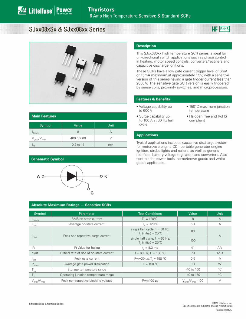
Schematic Symbol
Applications
Typical applications includes capacitive discharge system for motorcycle engine CDI, portable generator engine ignition, strobe lights and nailers, as well as generic rectifiers, battery voltage regulators and converters. Also controls for power tools, home/brown goods and white goods appliances.
A K
G
RoHS
Absolute Maximum Ratings — Sensitive SCRs
Symbol Parameter Test Conditions Value Unit
IT(RMS) RMS on-state current TC = 120°C 8 A
IT(AV) Average on-state current TC = 120°C 5.1 A
ITSM Peak non-repetitive surge current
single half cycle; f = 50 Hz; TJ (initial) = 25°C
83A
single half cycle; f = 60 Hz; TJ (initial) = 25°C
100
I2t I2t Value for fusing tp = 8.3 ms 41 A2s
di/dt Critical rate of rise of on-state current f = 60 Hz, TJ = 150 °C 70 A/μs
IGM Peak gate current Pw=20 μs, TJ = 150 °C 0.5 A
PG(AV) Average gate power dissipation TJ = 150 °C 0.1 W
TstgStorage temperature range -40 to 150 °C
TJ Operating junction temperature range -40 to 150 °C
VDSM/VRSM Peak non-repetitive blocking voltage Pw=100 μs VDRM/VRRM+100 V
Revised: 07/31/17
Specifications are subject to change without notice. ©2017 Littelfuse, Inc
Thyristors8 Amp High Temperature Sensitive & Standard SCRs
SJxx08xSx & SJxx08xx Series
Absolute Maximum Ratings — Standard SCRs
Symbol Parameter Test Conditions Value Unit
IT(RMS) RMS on-state current TC = 125 °C 8 A
IT(AV) Average on-state current TC = 125 °C 5.1 A
ITSM Peak non-repetitive surge current
single half cycle; f = 50 Hz; TJ (initial) = 25 °C
83A
single half cycle; f = 60 Hz; TJ (initial) = 25 °C
100
I2t I2t Value for fusing tp = 8.3 ms 41 A2s
di/dt Critical rate-of-rise of on-state current f = 60 Hz TJ = 150 °C 100 A/μs
IGM Peak gate current Pw=20 μs, TJ = 150°C 0.5 A
PG(AV) Average gate power dissipation TJ = 150 °C 0.1 W
Tstg Storage temperature range -40 to 150 °C
TJ Operating junction temperature range -40 to 150 °C
VDSM/VRSM Peak non-repetitive blocking voltage Pw=100 μs VDRM/VRRM+100 V
Electrical Characteristics (TJ = 25°C, unless otherwise specified) – Sensitive SCRs
Symbol Test ConditionsValue
UnitSJxx08xS2
IGTVD = 6V RL = 100 Ω
MIN. 20 μA
MAX. 200 μAVGT MAX. 0.8 Vdv/dt VD = VDRM; RGK = 220Ω ; TJ = 125°C MIN. 15 V/μs
VGD
VD = VDRM; RL = 3.3 kΩ; TJ = 125°C MIN. 0.2 V
VD = VDRM; RL = 3.3 kΩ; TJ = 150°C MIN. 0.1 VVGRM IGR = 10μA MIN. 6 VIH IT = 20mA (initial) MAX. 6 mAtq tp=50µs; dv/dt=5V/µs; di/dt=-30A/µs MAX. 130 μs
tgt IG = 2 x IGT; PW = 15µs; IT = 8A TYP. 6 μs
NOTE: xx = voltage
Symbol Test ConditionsValue
UnitSJxx08x1 SJxx08x
IGTVD = 12V RL = 60 Ω
MAX. 6 15 mAVGT MAX. 1.5 1.5 V
dv/dtVD = VDRM; gate open; TJ = 125°C
MIN.100 200
V/μsVD = VDRM; gate open; TJ = 150°C 50 120
VGD
VD = VDRM; RL = 3.3 kΩ; TJ = 125°C MIN. 0.2 0.2V
VD = VDRM; RL = 3.3 kΩ; TJ = 150°C MIN. 0.1 0.1IH IT = 200mA (initial) MAX. 20 30 mAtq IT=0.5A; tp=50µs; dv/dt=5V/µs; di/dt=-30A/µs MAX. 30 35 μs
tgt IG = 2 x IGT; PW = 15µs; IT = 8A TYP. 0.5 2 μs
NOTE: xx = voltage
Electrical Characteristics (TJ = 25°C, unless otherwise specified) – Standard SCRs
Revised: 07/31/17
Specifications are subject to change without notice. ©2017 Littelfuse, Inc
Thyristors8 Amp High Temperature Sensitive & Standard SCRs
SJxx08xSx & SJxx08xx Series
Static Characteristics
Symbol Test Conditions Value Unit
VTM IT = 16A; tp = 380 µs MAX. 1.6 V
IDRM / IRRM @ VDRM / VRRM
SJxx08xS2
TJ = 25°C 400 - 600V
MAX.
5
μA
TJ = 125°C, RGK = 220Ω 400 - 600V 1000
TJ = 150°C, RGK = 220Ω 400 - 600V 3000
SJxx08xx
TJ = 25°C 400 - 600V 10
TJ = 125°C 400 - 600V 1000
TJ = 150°C 400 - 600V 3000
Thermal Resistances
Symbol Parameter Value Unit
Rθ(J-C)Junction to case (AC)
SJxx08xS2 1.2°C/W
SJxx08xx 1.2
Note: xx = voltage
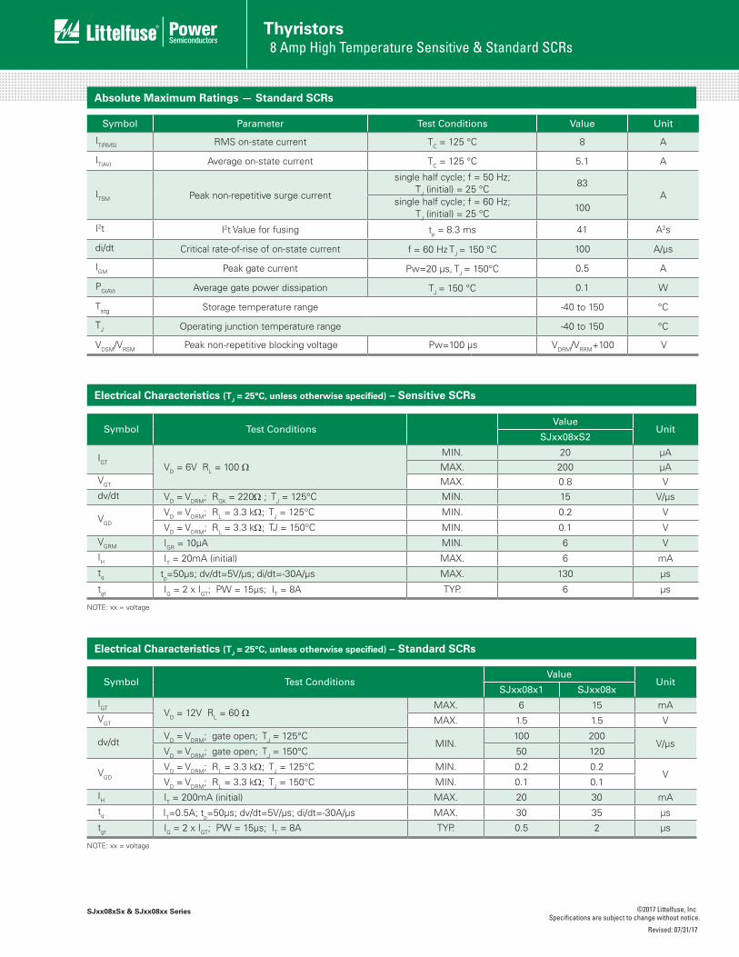
Figure 1: Normalized DC Gate Trigger Current vs. Junction Temperature (Sensitive SCR)
Figure 2: Normalized DC Gate Trigger Current vs. Junction Temperature (Standard SCR)
0
0.2
0.4
0.6
0.8
1
1.2
1.4
1.6
1.8
-40 -15 10 35 60 85 110 135 150
RGK=1K
RGK=220Ω
Junction Temperature (TJ) -- (°C)
Rat
io o
f I G
T /
I GT
(TJ =
25°
C)
Junction Temperature (TJ) -- (°C)
Rat
io o
f I G
T /
I GT (
TJ
= 25
°C)
0
0.2
0.4
0.6
0.8
1
1.2
1.4
1.6
1.8
-40 -15 10 35 60 85 110 135 150
= 2
5°C
)
0
0.5
1
1.5
2
2.5
-40 -15 10 35 60 85 110 135
Ratio
of I
H/ I
H(T
J
150
SJxx08xx
SJxx08xS2
Junction Temperature (TJ) -- (°C)Junction Temperature (TJ) -- (°C)
Rat
io o
f VG
T /
VG
T (
TJ =
25°
C)
0
0.2
0.4
0.6
0.8
1
1.2
1.4
-40 -15 10 35 60 85 110 135 150
SJxx08xS2
SJxx08xx
Figure 3: Normalized DC Gate Trigger Voltage vs. Junction Temperature
Figure 4: Normalized DC Holding Current vs. Junction Temperature
Revised: 07/31/17
Specifications are subject to change without notice. ©2017 Littelfuse, Inc
Thyristors8 Amp High Temperature Sensitive & Standard SCRs
SJxx08xSx & SJxx08xx Series
0
5
10
15
20
25
30
35
0.7 0.8 0.9 1 1.1 1.2 1.3 1.4 1.5 1.6 1.7
Inta
ntan
eous
On-
stat
e Cu
rren
t (I T
) –Am
ps
Instantaneous On-state Voltage (VT) – Volts
SJxx08xx
SJxx08DS2
0
2
4
6
8
10
12
14
0 2 4 6 8 10
Aver
age
On-
Stat
e Po
wer
[PD
(AV)
] -(W
atts
)
RMS On-State Current [I T(RMS)] - (Amps)
Diss
ipat
ion
SJxx08xx
SJxx08DS2
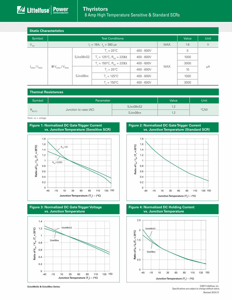
Figure 5: On-State Current vs. On-State Voltage (Typical)
Figure 6: Power Dissipation (Typical) vs. RMS On-State Current
Figure 7: Maximum Allowable Case Temperature vs. RMS On-State Current
Figure 8: Maximum Allowable Case Temperature vs. Average On-State Current
80
90
100
110
120
130
140
150
160
0 2 4 6 8 10
Max
imum
Allo
wab
leCa
se T
empe
ratu
re (T
C)-
RMS On-State Current [IT (RMS)] - (Amps)
°C
SJxx08xx
SJxx08DS2
Max
imum
Allo
wab
leCa
se T
empe
ratu
re (T
C)-
Average On-State Current [AV ] - (Amps)
°C
80
90
100
110
120
130
140
150
160
0 1 2 3 4 5 6
SJxx08xx
SJxx08DS2
Figure 9: Peak Capacitor Discharge Current
10
100
1000
0.5 1.0 10.0 50.0
Pulse Current Duration (tW) - ms
Peak
Dis
char
ge C
urr
ent
(IT
M)
- Am
ps
ITRM
tW
Revised: 07/31/17
Specifications are subject to change without notice. ©2017 Littelfuse, Inc
Thyristors8 Amp High Temperature Sensitive & Standard SCRs
SJxx08xSx & SJxx08xx Series
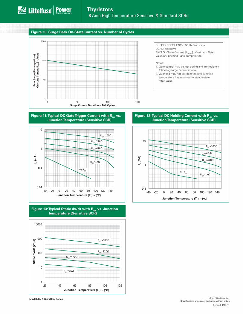
1
10
100
1000
1 10 100 1000
Peak
Sur
ge (N
on-r
epet
itiv
e)O
n-st
ate
Cur
rent
(ITS
M) –
Am
ps
Surge Current Duration -- Full Cycles
Figure 10: Surge Peak On-State Current vs. Number of Cycles
SUPPLY FREQUENCY: 60 Hz Sinusoidal LOAD: ResistiveRMS On-State Current: [IT(RMS)]: Maximum Rated Value at Specified Case Temperature
Notes:1. Gate control may be lost during and immediately
following surge current interval.2. Overload may not be repeated until junction
temperature has returned to steady-state rated value.
Figure 11: Typical DC Gate Trigger Current with RGK vs. Junction Temperature (Sensitive SCR)
0.01
0.1
1
10
-40 -20 0 20 40 60 80 100 120 140
I GT (m
A)
Junction Temperature (T ) -- (°C)
RGK=100Ω
RGK=470Ω
RGK=220Ω
RGK=1KΩ
No RGK
Figure 12: Typical DC Holding Current with RGK vs. Junction Temperature (Sensitive SCR)
0.1
1
10
-40 -20 0 20 40 60 80 100 120 140
I H (m
A)
Junction Temperature (T ) -- (°C)
RGK=100Ω
RGK=470Ω
RGK=220Ω
RGK=1KΩNo RGK
Figure 13: Typical Static dv/dt with RGK vs. Junction Temperature (Sensitive SCR)
1
10
100
1000
10000
25 45 65 85 105 125
Sta
tic d
v/dt
(V
/μs)
Junction Temperature (T ) -- (°C)
RGK=100Ω
RGK=470Ω
RGK=220Ω
RGK=1KΩ
Revised: 07/31/17
Specifications are subject to change without notice. ©2017 Littelfuse, Inc
Thyristors8 Amp High Temperature Sensitive & Standard SCRs
SJxx08xSx & SJxx08xx Series
Soldering Parameters
Reflow Condition Pb – Free assembly
Pre Heat
- Temperature Min (Ts(min)) 150°C
- Temperature Max (Ts(max)) 200°C
- Time (min to max) (ts) 60 – 180 secs
Average ramp up rate (Liquidus Temp) (TL) to peak
5°C/second max
TS(max) to TL - Ramp-up Rate 5°C/second max
Reflow- Temperature (TL) (Liquidus) 217°C
- Time (tL) 60 – 150 seconds
Peak Temperature (TP) 260+0/-5 °C
Time within 5°C of actual peak Temperature (tp)
20 – 40 seconds
Ramp-down Rate 5°C/second max
Time 25°C to peak Temperature (TP) 8 minutes Max.
Do not exceed 280°C
Time
Tem
pera
ture
TP
TLTS(max)
TS(min)
25
tP
tL
tS
time to peak temperature
PreheatPreheat
Ramp-upRamp-up
Ramp-downRamp-do
Physical Specifications Environmental Specifications
Test Specifications and Conditions
AC BlockingMIL-STD-750, M-1040, Cond A Applied Peak AC voltage for 1008 hours
Temperature CyclingMIL-STD-750, M-1051,100 cycles; -40°C to +150°C; 15-min dwell-time
Temperature/Humidity
EIA / JEDEC, JESD22-A1011008 hours; 160V - DC: 85°C; 85% rel humidity
High Temp StorageMIL-STD-750, M-1031,1008 hours; 150°C
Low-Temp Storage 1008 hours; -40°C
Resistance to Solder Heat
MIL-STD-750 Method 2031
Solderability ANSI/J-STD-002, category 3, Test A
Lead Bend MIL-STD-750, M-2036 Cond E
Moisture Sensitivity Level
Level 1, JEDEC-J-STD-020
Terminal Finish 100% Matte Tin-plated
Body MaterialUL Recognized epoxy meeting flammability rating V-0
Lead Material Copper Alloy
Design Considerations
Careful selection of the correct component for the application’s operating parameters and environment will go a long way toward extending the operating life of the Thyristor. Good design practice should limit the maximum continuous current through the main terminals to 75% of the component rating. Other ways to ensure long life for a power discrete semiconductor are proper heat sinking and selection of voltage ratings for worst case conditions. Overheating, overvoltage (including dv/dt), and surge currents are the main killers of semiconductors. Correct mounting, soldering, and forming of the leads also help protect against component damage.
Part Numbering System Part Marking System
CURRENT08: 8A
SENSITIVITY & TYPESensitive SCR:S2: 0.2mAStandard SCR:1: 6mA
PACKAGE TYPEV : TO-251 (VPAK)D : TO-252 (DPAK)
VOLTAGE RATING40 : 400V60 : 600V
SJ 60 08 D S2
COMPONENT TYPESJ: SCR
(blank): 15mAYMLDD
®
Date Code Marking Y:Year Code M: Month Code L: Location Code DD: Calendar Code
SJxx08DS2
Revised: 07/31/17
Specifications are subject to change without notice. ©2017 Littelfuse, Inc
Thyristors8 Amp High Temperature Sensitive & Standard SCRs
SJxx08xSx & SJxx08xx Series
Dimensions — TO-251AA (V/I-Package) — V/I-PAK Through Hole
DimensionInches Millimeters
Min Typ Max Min Typ Max
A 0.037 0.040 0.043 0.94 1.01 1.09
B 0.235 0.242 0.245 5.97 6.15 6.22
C 0.350 0.361 0.375 8.89 9.18 9.53
D 0.205 0.208 0.213 5.21 5.29 5.41
E 0.255 0.262 0.265 6.48 6.66 6.73
F 0.027 0.031 0.033 0.69 0.80 0.84
G 0.087 0.090 0.093 2.21 2.28 2.36
H 0.085 0.092 0.095 2.16 2.34 2.41
I 0.176 0.180 0.184 4.47 4.57 4.67
J 0.018 0.020 0.023 0.46 0.51 0.58
K 0.035 0.037 0.039 0.90 0.95 1.00
L 0.018 0.020 0.023 0.46 0.52 0.58
P 0.042 0.047 0.052 1.06 1.20 1.32
Q 0.034 0.039 0.044 0.86 1.00 1.11
R 0.034 0.039 0.044 0.86 1.00 1.11
S 0.074 0.079 0.084 1.86 2.00 2.11
AREA: 0.040 IN2TC MEASURING POINT
GATEG
I
E
D
A
B
C
F
J
H
K
L
5.28.208
5.34.210
Anode
Cathode
Anode
PQ
RS
Dimensions — TO-252AA (D-Package) — D-PAK Surface Mount
DimensionInches Millimeters
Min Typ Max Min Typ Max
A 0.037 0.040 0.043 0.94 1.01 1.09
B 0.235 0.243 0.245 5.97 6.16 6.22
C 0.106 0.108 0.113 2.69 2.74 2.87
D 0.205 0.208 0.213 5.21 5.29 5.41
E 0.255 0.262 0.265 6.48 6.65 6.73
F 0.027 0.031 0.033 0.69 0.80 0.84
G 0.087 0.090 0.093 2.21 2.28 2.36
H 0.085 0.092 0.095 2.16 2.33 2.41
I 0.176 0.179 0.184 4.47 4.55 4.67
J 0.018 0.020 0.023 0.46 0.51 0.58
K 0.035 0.037 0.039 0.90 0.95 1.00
L 0.018 0.020 0.023 0.46 0.51 0.58
M 0.000 0.000 0.004 0.00 0.00 0.10
N 0.021 0.026 0.027 0.53 0.67 0.69
O 0° 0° 5° 0° 0° 5°
P 0.042 0.047 0.052 1.06 1.20 1.32
Q 0.034 0.039 0.044 0.86 1.00 1.11
M
O
N
HJ
L
K
.1183
.0631.60
.0711.80
.2646.71
.2646.71
.1814.60
GATE
Anode
Cathode
Anode
TC MEASURING POINT
G
I
DE
A
B
C
F
5.28.208
5.34.210
: 0.040 IN2AREA
PQ
Revised: 07/31/17
Specifications are subject to change without notice. ©2017 Littelfuse, Inc
Thyristors8 Amp High Temperature Sensitive & Standard SCRs
SJxx08xSx & SJxx08xx Series
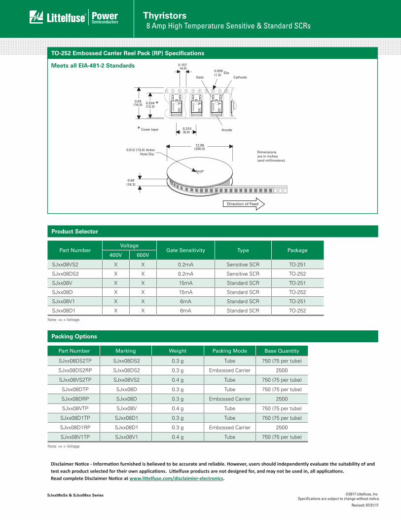
0.512 (13.0) ArborHole Dia.
XX
XX
XX
XX
XX
XX
XX
XX
XX
DC
XX
XX
XX
Gate Cathode
Anode
0.63(16.0)
0.157(4.0)
0.64(16.3)
12.99(330.0)
0.524(13.3)
0.315(8.0)
0.059 Dia(1.5)
*
* Cover tape
Direction of Feed
Dimensionsare in inches(and millimeters).
DC
DC
TO-252 Embossed Carrier Reel Pack (RP) Specifications
Meets all EIA-481-2 Standards
Product Selector
Part NumberVoltage
Gate Sensitivity Type Package400V 600V
SJxx08VS2 X X 0.2mA Sensitive SCR TO-251
SJxx08DS2 X X 0.2mA Sensitive SCR TO-252
SJxx08V X X 15mA Standard SCR TO-251
SJxx08D X X 15mA Standard SCR TO-252
SJxx08V1 X X 6mA Standard SCR TO-251
SJxx08D1 X X 6mA Standard SCR TO-252
Note: xx = Voltage
Packing Options
Part Number Marking Weight Packing Mode Base Quantity
SJxx08DS2TP SJxx08DS2 0.3 g Tube 750 (75 per tube)
SJxx08DS2RP SJxx08DS2 0.3 g Embossed Carrier 2500
SJxx08VS2TP SJxx08VS2 0.4 g Tube 750 (75 per tube)
SJxx08DTP SJxx08D 0.3 g Tube 750 (75 per tube)
SJxx08DRP SJxx08D 0.3 g Embossed Carrier 2500
SJxx08VTP SJxx08V 0.4 g Tube 750 (75 per tube)
SJxx08D1TP SJxx08D1 0.3 g Tube 750 (75 per tube)
SJxx08D1RP SJxx08D1 0.3 g Embossed Carrier 2500
SJxx08V1TP SJxx08V1 0.4 g Tube 750 (75 per tube)
Note: xx = Voltage
Disclaimer Notice - Information furnished is believed to be accurate and reliable. However, users should independently evaluate the suitability of and test each product selected for their own applications. Littelfuse products are not designed for, and may not be used in, all applications. Read complete Disclaimer Notice at www.littelfuse.com/disclaimier-electronics.