Embed Size (px)
Citation preview

Single-Chip, Multiband 3G Femtocell Transceiver
ADF4602
Rev. A Information furnished by Analog Devices is believed to be accurate and reliable. However, no responsibility is assumed by Analog Devices for its use, nor for any infringements of patents or other rights of third parties that may result from its use. Specifications subject to change without notice. No license is granted by implication or otherwise under any patent or patent rights of Analog Devices. Trademarks and registered trademarks are the property of their respective owners.
One Technology Way, P.O. Box 9106, Norwood, MA 02062-9106, U.S.A.Tel: 781.329.4700 www.analog.com Fax: 781.461.3113 ©2009–2011 Analog Devices, Inc. All rights reserved.
FEATURES Single-chip, multiband 3G transceiver
3GPP 25.104 release 9 WCDMA/HSPA compatible UMTS band coverage
Local area Class BS in Band I to Band VI and Band VIII to Band X
Direct conversion transmitter and receiver Minimal external components
Integrated, multiband, multimode monitoring No Tx SAW or Rx interstage SAW filters Integrated power management (3.1 V to 3.6 V supply) Integrated synthesizers, including PLL loop filters Integrated PA bias control DACs/GPOs
WCDMA and GSM receive baseband filter options Easy-to-use with minimal calibration
Automatic Rx DC offset control Simple gain, frequency, mode programming
Low supply current 50 mA typical Rx current 50 mA to 100 mA Tx current (varies with output power)
6 mm × 6 mm 40-pin LFCSP package
APPLICATIONS 3G home base stations (femtocells)
FUNCTIONAL BLOCK DIAGRAM
DA
C1
DA
C2
GPO
1 TO
4
Tx_PWR_CONTROL
Tx_PWR_CONTROL
TXBBIBTXBBI
TXBBQTXBBQB
VSUP7
VSUP6
RXBBIRXBBIB
VDD
RXLBRF
RXHB2RF
RXHB1RF
TXLBRF
RXBBQRXBBQB
DA
C1
DA
C2
GPO
[4:1
]
Tx_PWR_CONTROL
Tx_PWR_CONTROL
TXHBRF
LOOPFILTER
Rx PLL
Rx_LO_LBSELECTABLE BANDWIDTH
BASEBAND FILTERS
Rx_LO_LB
FRAC NSYNTHE-
SIZERLO GENERATOR
LOOPFILTER
FRAC NSYNTHE-
SIZERLO GENERATOR
DC OFFSETCORRECTION
SERIALINTER-FACE
DC OFFSETCORRECTION
QCHAN-
NEL
ICHAN-
NEL
VSUP8
26MHz 19.2MHz
ADF4602
VIN
TR
EFC
LK
CH
IPC
LK
VSU
P2
LDO2
VSU
P3
LDO3
VSU
P4
LDO4
VSU
P5
LDO5
Tx PLL
0709
2-00
1
VSU
P1
LDO1
REFIN
SEN
SCLK
SDA
TA
Figure 1.

ADF4602
Rev. A | Page 2 of 36
TABLE OF CONTENTS Features .............................................................................................. 1
Applications....................................................................................... 1
Functional Block Diagram .............................................................. 1
Revision History ............................................................................... 2
General Description ......................................................................... 3
Specifications..................................................................................... 4
Timing Characteristics..................................................................... 8
Absolute Maximum Ratings............................................................ 9
ESD Caution.................................................................................. 9
Pin Configuration and Function Descriptions........................... 10
Typical Performance Characteristics ........................................... 12
Theory of Operation ...................................................................... 19
Transmitter Description ............................................................ 19
DACs ............................................................................................ 20
General Purpose Outputs.......................................................... 20
Receiver Description.................................................................. 20
Power Management ................................................................... 23
Frequency Synthesis................................................................... 24
Serial Port Interface (SPI).............................................................. 25
Operation and Timing............................................................... 25
Registers........................................................................................... 26
Register Map ............................................................................... 26
Register Description .................................................................. 27
Software Initialization Procedure................................................. 31
Initialization Sequence .............................................................. 31
Applications Information .............................................................. 33
Interfacing the ADF4602 to the AD9963................................ 33
Outline Dimensions ....................................................................... 35
Ordering Guide .......................................................................... 35
REVISION HISTORY 2/11—Rev. 0 to Rev. A
Changes to Features and Applications........................................... 1 Changes to Table 1............................................................................ 4 Changes to Table 3............................................................................ 9 Changes to Figure 4........................................................................ 10 Changes to Figure 13...................................................................... 13 Changes to Figure 21 and Figure 22............................................. 14 Changes to Figure 26 and Figure 27............................................. 15 Changes to Figure 31 through Figure 33 ..................................... 16 Changes to Figure 44...................................................................... 21 Changes to DC Offset Compensation Section ........................... 23 Changes to Figure 51...................................................................... 26 Changes to Table 13........................................................................ 30 Replaced Applications Information Section ............................... 33 Changes to Figure 53...................................................................... 34
10/09—Revision 0: Initial Version
ADF4602
Rev. A | Page 3 of 36
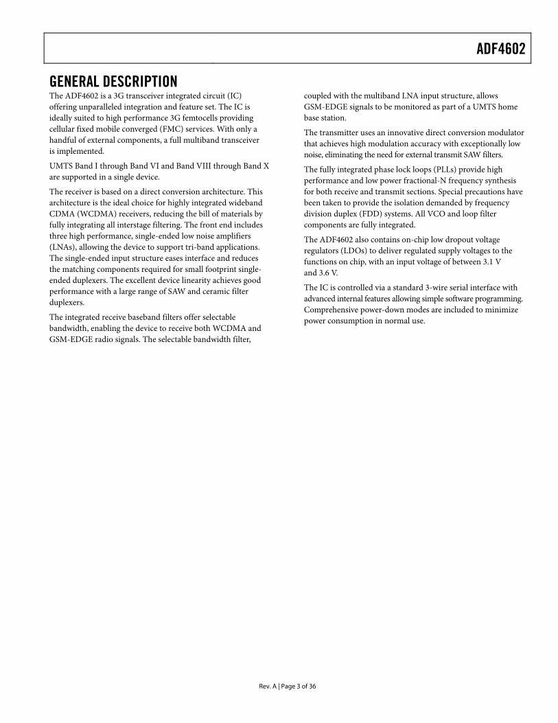
GENERAL DESCRIPTION The ADF4602 is a 3G transceiver integrated circuit (IC) offering unparalleled integration and feature set. The IC is ideally suited to high performance 3G femtocells providing cellular fixed mobile converged (FMC) services. With only a handful of external components, a full multiband transceiver is implemented.
UMTS Band I through Band VI and Band VIII through Band X are supported in a single device.
The receiver is based on a direct conversion architecture. This architecture is the ideal choice for highly integrated wideband CDMA (WCDMA) receivers, reducing the bill of materials by fully integrating all interstage filtering. The front end includes three high performance, single-ended low noise amplifiers (LNAs), allowing the device to support tri-band applications. The single-ended input structure eases interface and reduces the matching components required for small footprint single-ended duplexers. The excellent device linearity achieves good performance with a large range of SAW and ceramic filter duplexers.
The integrated receive baseband filters offer selectable bandwidth, enabling the device to receive both WCDMA and GSM-EDGE radio signals. The selectable bandwidth filter,
coupled with the multiband LNA input structure, allows GSM-EDGE signals to be monitored as part of a UMTS home base station.
The transmitter uses an innovative direct conversion modulator that achieves high modulation accuracy with exceptionally low noise, eliminating the need for external transmit SAW filters.
The fully integrated phase lock loops (PLLs) provide high performance and low power fractional-N frequency synthesis for both receive and transmit sections. Special precautions have been taken to provide the isolation demanded by frequency division duplex (FDD) systems. All VCO and loop filter components are fully integrated.
The ADF4602 also contains on-chip low dropout voltage regulators (LDOs) to deliver regulated supply voltages to the functions on chip, with an input voltage of between 3.1 V and 3.6 V.
The IC is controlled via a standard 3-wire serial interface with advanced internal features allowing simple software programming. Comprehensive power-down modes are included to minimize power consumption in normal use.

ADF4602
Rev. A | Page 4 of 36
SPECIFICATIONS VDD = 3.1 V to 3.6 V, GND = 0 V, TA = TMIN to TMAX, unless otherwise noted. Typical specifications are at VDD = 3.3 V and TA = 25°C, 26 MHz reference input level = 0.7 V p-p.
Table 1. Parameter Min Typ Max Unit Test Conditions REFERENCE SECTION
Reference Input Reference Input Frequency 26 MHz Reference Input Amplitude 0.1 0.7 2.0 V p-p Single-ended operation, dc-coupled1 Reference Input Jitter 1.5 ps rms
REFCLK Output (26 MHz) Output Load Capacitance 10 40 pF Output Swing 1.5 V p-p 10 pF load Output Slew Rate 200 V/μs 10 pF load Output Duty Cycle Variation 2 % Input duty cycle = 50% Output Jitter 1.5 ps rms
CHIPCLK Output (19.2 MHz) Output Load Capacitance 10 40 pF Frequency Multiplication Ratio 48/65 48/65 N/A Output Swing 1.5 V p-p 10 pF load Output Duty Cycle Variation 2 % Input duty cycle = 50% Output Jitter 33 ps rms Lock Time 50 μs
TRANSMIT SECTION I/Q Input
Input Resistance 100 kΩ Single-ended Input Capacitance 2 pF Single-ended Differential Peak Input Voltage 500 550 mV pd Input Common-Mode Voltage 1.05 1.2 1.4 V Baseband Filter 3 dB Bandwidth 4.0 MHz
TX Gain Control Maximum Gain 5 dB 1 V p-p differential baseband input Gain Control Range 60 dB Gain Control Resolution 1/32 dB Average of LSB steps Gain Control Accuracy 1.0 dB Any 1 dB step
10 dB Any 10 dB step Gain Settling Time 1 μs POUT within 0.1 dB of final value
RF Specifications (High Band) Carrier Frequency 1710 2170 MHz Output Impedance 50 Ω Output Power (POUT) −8 dBm TM1 signal 64 DPCH Output Noise Spectral Density −155 dBc/Hz 40 MHz offset −161 dBc/Hz 80 MHz offset −161 dBc/Hz 95 MHz offset −163 dBc/Hz 190 MHz offset Carrier Leakage −35 dBc POUT = −8 dBm FDD EVM 5 % POUT = −8 dBm FDD ACLR 55 dB ±5 MHz, POUT = −8 dBm 70 dB ±10 MHz, POUT = −8 dBm
ADF4602
Rev. A | Page 5 of 36
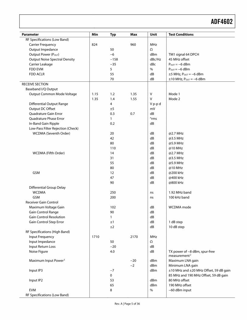
Parameter Min Typ Max Unit Test Conditions RF Specifications (Low Band)
Carrier Frequency 824 960 MHz Output Impedance 50 Ω Output Power (POUT) −6 dBm TM1 signal 64 DPCH Output Noise Spectral Density −158 dBc/Hz 45 MHz offset Carrier Leakage −35 dBc POUT = −6 dBm FDD EVM 5 % POUT = −6 dBm FDD ACLR 55 dB ±5 MHz, POUT = −6 dBm 70 dB ±10 MHz, POUT = −6 dBm
RECEIVE SECTION Baseband I/Q Output
Output Common Mode Voltage 1.15 1.2 1.35 V Mode 1 1.35 1.4 1.55 V Mode 2 Differential Output Range 4 V p-p d Output DC Offset ±5 mV Quadrature Gain Error 0.3 0.7 dB Quadrature Phase Error 1 °rms In-Band Gain Ripple 0.2 dB Low-Pass Filter Rejection (Check)
WCDMA (Seventh Order) 20 dB @2.7 MHz 42 dB @3.5 MHz 80 dB @5.9 MHz 110 dB @10 MHz WCDMA (Fifth Order) 14 dB @2.7 MHz
31 dB @3.5 MHz 55 dB @5.9 MHz 80 dB @10 MHz
GSM 12 dB @200 kHz 47 dB @400 kHz 90 dB @800 kHz
Differential Group Delay WCDMA 250 ns 1.92 MHz band GSM 200 ns 100 kHz band
Receiver Gain Control Maximum Voltage Gain 102 dB WCDMA mode Gain Control Range 90 dB Gain Control Resolution 1 dB Gain Control Step Error ±1 dB 1 dB step ±2 dB 10 dB step
RF Specifications (High Band) Input Frequency 1710 2170 MHz Input Impedance 50 Ω Input Return Loss −20 dB Noise Figure 4.0 dB TX power of −8 dBm, spur-free
measurement2 Maximum Input Power3 −20 dBm Maximum LNA gain −2 dBm Minimum LNA gain Input IP3 −7 dBm ±10 MHz and ±20 MHz Offset, 59 dB gain 0 85 MHz and 190 MHz Offset, 59 dB gain Input IP2 53 dBm 80 MHz offset 65 dBm 190 MHz offset EVM 8 % −60 dBm input
RF Specifications (Low Band)

ADF4602
Rev. A | Page 6 of 36
Parameter Min Typ Max Unit Test Conditions Input Frequency 824 960 MHz Input Impedance 50 Ω Input Return Loss −20 dB Noise Figure 4.0 dB 80 dB gain, TX power of −8 dBm Maximum Input Power3 −20 dBm Maximum LNA gain −2 dBm Minimum LNA gain Input IP3 2 dBm ±10 MHz and ±20 MHz offset, 59 dB gain 5 dBm 45 MHz and 90 MHz offset, 59 dB gain Input IP2 40 dBm 45 MHz offset EVM 7 % −60 dBm input
Synthesizer Section Channel Resolution 50 kHz Lock Time3 200 μs
DAC/GPO CONTROL DAC1
Resolution 5 bits Output Range 2.3 3.15 V VDD > 3.15 V Absolute Accuracy ±50 mV Any code, VDD > 3.2 V Output LSB Step 25 mV Output Capacitive Load 1 nF Output Current −10 +10 mA Output Impedance 1 Ω
DAC2 Resolution 6 bits Output Range 0 2.85 V DNL ±0.5 LSB No load INL ±1.0 LSB No load Output Capacitive Load 1 nF Output Current −5 +5 mA Output Impedance 5 Ω
GPO1 to GPO4 Output Current 2 mA GPO1, GPO2, GPO3 10 mA GPO4 Output High Voltage 2.6 V Maximum output current Output Low Voltage 0.2 V Maximum output current Switching Time 1 μs 5 pF load
LOGIC INPUTS Input High Voltage, VINH 1.2 2.1 V 1.8 V readback mode4 Input High Voltage, VINH 1.2 3.3 V 2.8 V readback mode4 Input Low Voltage, VINL 0.6 V Input Current, IINH/IINL ±1 μA Input Capacitance, CIN 10 pF
LOGIC OUTPUTS (SDATA) Output High Voltage, VOH VX − 0.45 V VX = VINT or VSUP8, IOH = 500 μA Output Low Voltage, VOL 0.45 V IOL = 500 μA CLKOUT Rise/Fall 5 ns CLKOUT Load 10 pF
TEMPERATURE RANGE (TA) 0 85 °C
ADF4602
Rev. A | Page 7 of 36
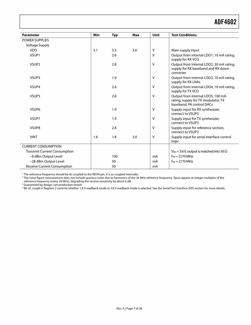
Parameter Min Typ Max Unit Test Conditions POWER SUPPLIES
Voltage Supply VDD 3.1 3.3 3.6 V Main supply input VSUP1 2.6 V Output from internal LDO1, 10 mA rating,
supply for RX VCO VSUP2 2.8 V Output from Internal LDO2, 30 mA rating,
supply for RX baseband and RX down-converter
VSUP3 1.9 V Output from internal LDO3, 10 mA rating, supply for RX LNAs
VSUP4 2.6 V Output from internal LDO4, 10 mA rating, supply for TX VCO
VSUP5 2.8 V Output from internal LDO5, 100 mA rating, supply for TX modulator, TX baseband, PA control DACs
VSUP6 1.9 V Supply input for RX synthesizer, connect to VSUP3
VSUP7 1.9 V Supply input for TX synthesizer, connect to VSUP3
VSUP8 2.8 V Supply input for reference section, connect to VSUP2
VINT 1.6 1.8 2.0 V Supply input for serial interface control logic
CURRENT CONSUMPTION Transmit Current Consumption VDD = 3.6 V, output is matched into 50 Ω
−8 dBm Output Level 100 mA FRF = 2170 MHz −28 dBm Output Level 50 mA FRF = 2170 MHz
Receive Current Consumption 50 mA 1 The reference frequency should be dc coupled to the REFIN pin. It is ac-coupled internally. 2 The noise figure measurement does not include spurious noise due to harmonics of the 26 MHz reference frequency. Spurs appear at integer multiples of the
reference frequency (every 26 MHz), degrading the receive sensitivity by about 6 dB. 3 Guaranteed by design, not production tested. 4 Bit sif_vsup8 in Register 2 controls whether 1.8 V readback mode or 2.8 V readback mode is selected. See the S section for more details. erial Port Interface (SPI)
ADF4602
Rev. A | Page 8 of 36
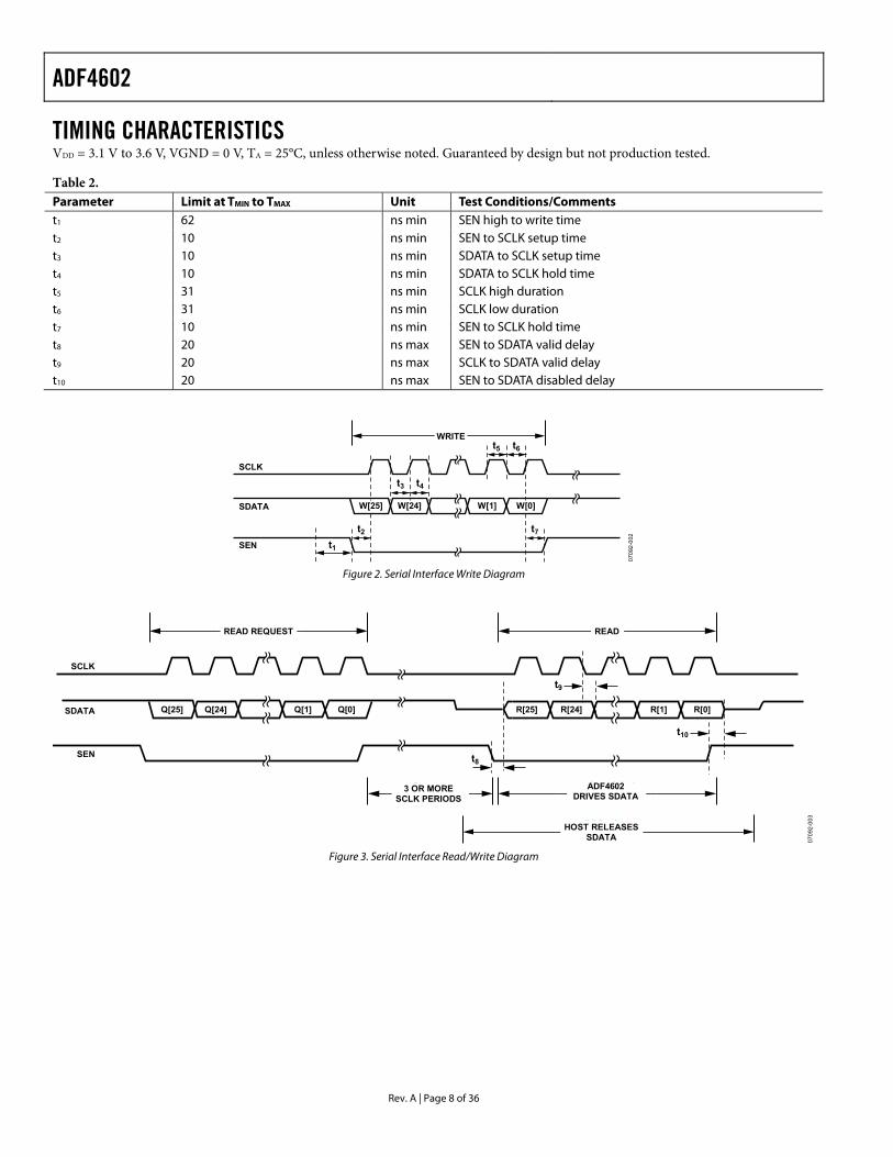
TIMING CHARACTERISTICS VDD = 3.1 V to 3.6 V, VGND = 0 V, TA = 25°C, unless otherwise noted. Guaranteed by design but not production tested.
Table 2. Parameter Limit at TMIN to TMAX Unit Test Conditions/Comments t1 62 ns min SEN high to write time t2 10 ns min SEN to SCLK setup time t3 10 ns min SDATA to SCLK setup time t4 10 ns min SDATA to SCLK hold time t5 31 ns min SCLK high duration t6 31 ns min SCLK low duration t7 10 ns min SEN to SCLK hold time t8 20 ns max SEN to SDATA valid delay t9 20 ns max SCLK to SDATA valid delay t10 20 ns max SEN to SDATA disabled delay
W[25] W[24] W[1]
SCLK
SDATA
SEN
W[0]
WRITE
t3
t2 t7
t1
t4
t6t5
0709
2-00
2
Figure 2. Serial Interface Write Diagram
Q[25] Q[24] Q[1]
SCLK
SDATA
SEN
Q[0] R[25] R[24] R[1] R[0]
3 or moreSYSCLK periods
DBB releasesRSDATA
selected devicedrives RSDATA
READREAD REQUEST
0709
2-00
3
t8
t10
t9
3 OR MORESCLK PERIODS
HOST RELEASESSDATA
ADF4602DRIVES SDATA
Figure 3. Serial Interface Read/Write Diagram

ADF4602
Rev. A | Page 9 of 36
ABSOLUTE MAXIMUM RATINGS TA = 25°C, unless otherwise noted.
Table 3. Parameter Rating VDD to GND −0.3 V to +4 V VSUP1, VSUP2 to GND −0.3 V to +3.6 V VSUP4, VSUP5, VSUP6, VSUP7, VSUP8, VSUP9 to GND
−0.3 V to +3.6 V
VSUP3 to GND −0.3 V to +2.0 V VINT to GND −0.3 V to +2.0 V Analog I/O Voltage to GND −0.3 V to VDD + 0.3 V Digital I/O Voltage to GND −0.3 V to VDD + 0.3 V Operating Temperature Range
Commercial (B Version) 0°C to +85°C Storage Temperature Range −65°C to +125°C Maximum Junction Temperature 150°C LFCSP θJA Thermal Impedance 32°C/W Reflow Soldering Based on J-STD-020
Peak Temperature 260°C Number of Reflows 3 Time at Peak Temperature 40 sec
Stresses above those listed under Absolute Maximum Ratings may cause permanent damage to the device. This is a stress rating only; functional operation of the device at these or any other conditions above those indicated in the operational section of this specification is not implied. Exposure to absolute maximum rating conditions for extended periods may affect device reliability.
This device is a high performance RF integrated circuit with an ESD rating of <2 kV, and it is ESD sensitive. Proper precautions should be taken for handling and assembly.
ESD CAUTION

ADF4602
Rev. A | Page 10 of 36
PIN CONFIGURATION AND FUNCTION DESCRIPTIONS
NOTES1. NC = NO CONNECT. DO NOT CONNECT TO THIS PIN.2. THE EXPOSED PADDLE MUST BE CONNECTED TO GROUND FOR CORRECT CHIP OPERATION. IT PROVIDES BOTH A THERMAL AND ELECTRICAL CONNECTION TO THE PCB. 07
092-
004
1GPO32VSUP13VSUP34RXLBRF5NC6RXHB2RF7RXHB1RF8RXBBI9RXBBIB
10RXBBQ
23 TXBBQB24 TXLBRF25 TXRFGND26 TXHBRF27 TXRFGND28 VSUP529 DAC230 DAC1
22 TXBBQ21 VSUP4
11R
XBB
QB
12VS
UP2
13VI
NT
15SC
LK
17N
C16
SEN
18VS
UP7
19TX
BB
I20
TXB
BIB
14SD
ATA
33C
HIP
CLK
34VS
UP8
35R
EFC
LK36
REF
IN37
NC
38VS
UP6
39G
PO1
40G
PO2
32G
PO4
31VD
D
ADF4602TOP VIEW
(Not to Scale)
PIN 1INDICATOR
Figure 4. Pin Configuration
Table 4. Pin Function Descriptions Pin No. Mnemonic Function 1 GPO3 General Purpose Output 3. Digital output. This is used for external switch or PA control. 2 VSUP11 Output from LDO 1. Supply for receive VCO. Nominal value of 2.6 V. 100 nF decoupling to ground is required. 3 VSUP31 Output from LDO 3. Supply for receive LNA. Nominal value of 1.9 V. 100 nF decoupling to ground is required. 4 RXLBRF Receive Low Band LNA Input. 5 NC No Connect. Do not connect to this pin. 6 RXHB2RF Receive Second High Band LNA Input. Use for UMTS Band II. 7 RXHB1RF Receive First High Band LNA Input. Use for UMTS Band I. 8 RXBBI Receive Baseband I Output. 9 RXBBIB Complementary Receive Baseband I Output. 10 RXBBQ Receive Baseband Q Output. 11 RXBBQB Complementary Receive Baseband Q Output. 12 VSUP21 Output from LDO 2. Supply for receive downconverter and baseband. Nominal value of 2.8 V. 100 nF
decoupling to ground is required. 13 VINT Serial Port Supply Input. 1.8 V should be applied to this pin. 14 SDATA Serial Port Data Pin. This can be an input or output. 15 SCLK Serial Clock Input. 16 SEN Serial Port Enable Input. 17 NC No Connect. Do not connect to this pin. 18 VSUP71 Transmit Synthesizer Supply Input. Connect to VSUP3 and decouple with 100 nF to ground. 19 TXBBI Transmit Baseband I Input. 20 TXBBIB Complementary TX Baseband I Input. 21 VSUP41 Output from LDO4. Supply for transmit VCO. Nominal value of 2.8 V. 100 nF decoupling to GND is required. 22 TXBBQ Transmit Baseband Q Input. 23 TXBBQB Complementary TX Baseband Q Input. 24 TXLBRF Low Band Transmit RF Output. This can output in the range of 824 MHz to 960 MHz. 25 TXRFGND Transmit RF Ground. Connect this pin to ground. 26 TXHBRF High Band Transmit RF Output. This can output in the range of 1710 MHz to 2170 MHz. 27 TXRFGND Transmit RF Ground. Connect this pin to ground. 28 VSUP51 Output from LDO 5. Supply for transmit modulator, baseband, power detector, and DACs. Nominal value of
2.8 V. 100 nF decoupling to ground is required. 29 DAC2 Output from DAC2. 30 DAC1 Output from DAC1.

ADF4602
Rev. A | Page 11 of 36
Pin No. Mnemonic Function 31 VDD Main Supply Input. 32 GPO4 Digital Output. This is used for switch or PA control. 33 CHIPCLK Chip Clock Output. 34 VSUP81 Reference Clock Supply Input. Connect to VSUP2, and decouple to ground with 100 nF. 35 REFCLK Reference Clock Output. 36 REFIN Reference Clock Input. The reference is ac-coupled internally. 37 NC No Connect. Do not connect to this pin. 38 VSUP61 Receive Synthesizer Supply Input. Connect to VSUP3 and decouple to ground with 100 nF. 39 GPO1 Digital Output. This is used for switch or PA control. 40 GPO2 Digital Output. This is used for switch or PA control. EPAD Exposed Paddle Under Chip. This must be connected to ground for correct chip operation. It provides both a
thermal and electrical connection to the PCB.
1Y5V capacitors are not recommended for use with these pins. X7R, X5R, C0G or a similar type of capacitor should be used.

ADF4602
Rev. A | Page 12 of 36
TYPICAL PERFORMANCE CHARACTERISTICS
A
B
3DB
Ref3.90
dBm
Ref3.90
dBm
Ref3.90
dBm
Att*0 dBAtt*0 dB
Code Power Relative
CF 2.1399994 GH CPICH Slot 0Chan Code 0
3DB
1VIEW
Chan Slot 0
Ref3.90
dBm
Ref3.90
dBm
Ref3.90
dBm
1CLRWR
Result Summary
CF 2.1399994 GH CPICH Slot 0Chan Code 5Chan Slot 0
Att*0 dBAtt*0 dB
Start Ch 0 64 Ch/ Stop Ch 511
SR 240 ksps
SR 240 ksps
-63
-56
-49
-42
-35
-28
-21
-14
-7
GLOBAL RESULTS FOR FRAME 0:Total PowerChip Rate ErrorIQ OffsetComposite EVMCPICH Slot No
-8.030.951.832.54
0
dBmppm%%
Carrier Freq ErrorTrigger to FrameIQ ImbalancePk CDE (15 ksps)No of Active Chan
65.989.642977
0.23-50.12
44
Hzms%dB
CHANNEL RESULTSSymbol RateChannel CodeNo of Pilot BitsChannel Power RelSymbol EVM
240.0050
-0.042.43
ksps
dB% rms
Timing OffsetChannel Slot NoModulation TypeChannel Power AbsSymbol EVM
RHO00
16QAM-19.05
7.02
0.99936Chips
dBm% Pk
0709
2-00
6
Figure 5. UMTS Band I Transmit EVM, Test Model 5, 2.5% EVM
CPICH Slot 0
SR 15 kspsChan Code 0Chan Slot 0
B
LNLN
CF 881.5 MHzResult Summary
dB
CF 881.5 MHzCode Pwr RelativeCode Pwr RelativeCPICH Slot 0CPICH Slot 0
SR 15 kspsChan Code 0Chan Code 0Chan Slot 0Chan Slot 0
2
2
A
LN
Ref LvlRef Lvl6 dBm
Ref LvlRef Lvl6 dBm
START: CH 0 STOP: CH 51164 CH/DIV
Ref LvlRef Lvl6 dBm
Ref LvlRef Lvl6 dBm
-63
-56
-49
-42
-35
-28
-21
-7
-70
0
RESULT SUMMARY
GLOBAL RESULTS ³Total PWR -4.57 dBm ³ Carr Freq Err -92.42 HzChip Rate Err 1.04 ppm ³ Trg to Frame 22.62 æsIQ Offset 0.79 % ³ IQ Imbalance 0.36 %Composite EVM 2.04 % rms ³ Pk Code Dom Err -49.96 dB rmsCPICH Slot Number 0 ³ ( 15 ksps)
CHANNEL RESULTS ³Symb Rate 15 ksps ³ Timing Offset 0 ChipsChannel Code 0 ³ Chan Slot Number 0Modulation Type QPSK ³ No. of Pilot Bits 0Chan Pow rel. 0.00 dB ³ Chan Pow abs. -14.60 dBmSymbol EVM 0.74 % rms ³ Symbol EVM 1.21 % Pk 07
092-
005
↓
Figure 6. UMTS Band V Transmit EVM, Test Model 1, 64 DPCH, 2% EVM
20
18
16
14
12
10
8
6
4
2
0–35 –30 –25 –20 –15 –10 –5 0 5
txpwr_set (dBm)
CO
MPO
SITE
EVM
(%)
0709
2-00
7
DUT 1DUT 4DUT 6DUT 8DUT 10
DUT 2DUT 5DUT 7DUT 9DUT 3
30dB DYNAMIC RANGE <6% EVM
Figure 7. TXHBRF, UMTS Band I. Transmit EVM vs. txpwr_set (dBm), Measured Across 10 DUTS, Four Calibration Points Applied, Transmit Frequency 2140 MHz
0
2
4
6
8
10
12
14
16
18
20
–35 –30 –25 –20 –15 –10 –5 0 5
CO
MPO
SITE
EVM
(%)
txpwr_set (dBm) 0709
2-10
7
Figure 8. TXHBRF, UMTS Band II. Transmit EVM vs. txpwr_set (dBm),
Four Calibration Points Applied, Transmit Frequency 1960 MHz.
0
2
4
6
8
10
12
14
16
18
20
–35 –30 –25 –20 –15 –10 –5 0 5
CO
MPO
SITE
EVM
(%)
txpwr_set (dBm) 0709
2-10
8
Figure 9. TXLBRF,UMTS Band V, Transmit EVM vs. tpwr_set (dBm),
Four Calibration Points Applied, Transmit Frequency 881 MHz.
–30
–35
–40
–45
–50
–55
–60
–65
–70–14 –12 –10 –8 –6 –4
OUTPUT POWER (dBm/3.84MHz)
AC
LR (d
B)
0709
2-00
8
+5MHz–5MHz+10MHz–10MHz
Figure 10. TXHBRF Transmit ACLR vs. Output Power, Test Model 1 Signal, 10.54 dB PAR, 2170 MHz

ADF4602
Rev. A | Page 13 of 36
–30
–35
–40
–45
–50
–55
–60
–65
–70–25 –20 –15 –10 –5 0
OUTPUT POWER (dBm/3.84MHz)
AC
LR (d
B)
+5MHz–5MHz+10MHz–10MHz
0709
2-00
9
Figure 11. TXLBRF Transmit ACLR vs. Output Power, Test Model 1 Signal,
10.54 dB PAR, 881 MHz
REF –12.7dBm *ATT 0dB
*RBW 30kHz*VBW 300kHz*SWT 100ms
CENTER 2.14GHz 2.55MHz/DIV SPAN 25.5MHz 0709
2-01
0
–20
–30
–40
–50
–60
–70
–80
–90
–100
–110
POS –12.698dBm CH PWRACP LOWACP UPALT1 LOWALT1 UP
–8.08dBm–57.05dBm–57.09dBm–70.92dBm–71.41dBm
Figure 12. TXHBRFTransmit ACLR, UMTS Band I, 2140 MHz
2.6MHz/ SPAN 26MHz 0709
2-11
0
REF –20dBm *ATT 5dB
*RBW 30kHz*VBW 300kHz*SWT 100ms
CENTER 1.96GHz
CH PWRACP LOWACP UPALT1 LOWALT1 UP
–8.44dBm–57.07dBm–58.02dBm–66.31dBm–66.08dBm
–20
–30
–40
–50
–60
–70
–80
–90
–100
–110
Figure 13. TXHBRFTransmit ACLR, UMTS Band II, 1960 MHz
REF –10.9dBm *ATT 5dB
*RBW 30kHz*VBW 300kHz*SWT 100ms
MARKER 1 (T1)–23.01dBm
880.877403846MHz
CENTER 881MHz 2.55MHz/DIV SPAN 25.5MHz 0709
2-01
1
–20
–30
–40
–50
–60
–70
–80
–90
–100
–110
POS –10.895dBm CH PWRACP LOWACP UPALT1 LOWALT1 UP
–4.39dBm–60.63dBm–58.52dBm–72.07dBm–72.13dBm
Figure 14. TXLBRF Transmit ACLR, UMTS Band V, 881 MHz
–51
–53
–55
–57
–59
–61
–63
–652110 2120 2130 2140 2150 2160 2170
FREQUENCY (MHz)
5MH
z A
CLR
(dB
)
0709
2-01
2
0°C 5MHz HIGH25°C 5MHZ HIGH85°C 5MHz HIGH
0°C 5MHz LOW25°C 5MHz LOW85°C 5MHz LOW
Figure 15. Transmit ACLR vs. Frequency and Temperature (UMTS Band I),
Transmit Output Power = −8 dBm
–51
–53
–55
–57
–59
–61
–63
–651930 1940 1950 1960 1970 1980 1990
FREQUENCY (MHz)
5MH
z A
CLR
(dB
)
0709
2-01
3
0°C 5MHz HIGH25°C 5MHZ HIGH85°C 5MHz HIGH
0°C 5MHz LOW25°C 5MHz LOW85°C 5MHz LOW
Figure 16. Transmit ACLR vs. Frequency and Temperature (UMTS Band II),
Transmit Output Power = −8 dBm

ADF4602
Rev. A | Page 14 of 36
–54
–56
–58
–60
–62
–64
–66865 870 875 880 885 890 895
FREQUENCY (MHz)
5MH
z A
CLR
(dB
)
0709
2-01
4
0°C 5MHz HIGH25°C 5MHZ HIGH85°C 5MHz HIGH
0°C 5MHz LOW25°C 5MHz LOW85°C 5MHz LOW
Figure 17. Transmit ACLR vs. Frequency and Temperature (UMTS Band V),
Transmit Output Power = −7 dBm
5
0
–5
–10
–15
–20
–25
–30
–35
–400.1 1 10 100
FREQUENCY (MHz)
MA
GN
ITU
DE
(dB
m)
0709
2-01
5
Figure 18. Transmit Baseband Filter Response
–70
–80
–90
–100
–110
–120
–130
–140
–150
–160
–1701k 10k 100k 1M 10M 100M
OFFSET FREQUENCY (Hz)
PHA
SE N
OIS
E (d
Bc/
Hz)
0709
2-01
6
Figure 19. Transmit Synthesizer Phase Noise
0.14
0.12
0.10
0.08
0.06
0.04
0.02
0–34 –32 –30 –28 –26 –24 –22 –20 –18 –16 –14 –12 –10 –8 –6 –4
OUTPUT POWER (dBm/3.84MHz)
CU
RR
ENT
CO
NSU
MPT
ION
(A)
0709
2-01
7
Figure 20. Current Consumption vs. Transmit Output Power; Frequency =
2170 MHz, VDD = 3.3 V, Test Model 5 Signal, Receiver Disabled
–120
–100
–80
–60
–40
–20
0
0.1 1 10
MA
GN
ITU
DE
(dB
)
FREQUENCY (MHz) 0709
2-11
8
Figure 21. Receive WCDMA Baseband Filter Response
10
0
–10
–20
–30
–40
–50
–60
–70
–80
–90
–10010 100 1000
FREQUENCY (kHz)
MA
GN
ITU
DE
(dB
m)
0709
2-01
9
Figure 22. Receive GSM Baseband Filter Response

ADF4602
Rev. A | Page 15 of 36
16
14
12
10
8
6
4
2
020 30 40 50 60 70 80 90
RECEIVE GAIN SETTING (dB)
EVM
(%)
0709
2-02
0
MIXSTEP = 10LNASTEP = 6GAINCAL = 8
Figure 23. Receive EVM vs. Gain; 2.84 MHz QPSK Modulated Input Signal,
WCDMA Receive Baseband Filter
2.0
1.8
1.6
1.4
1.2
1.0
0.8
0.6
0.4
0.2
020 30 40 50 60 70 80 90 100
RECEIVE GAIN SETTING (dB)
GA
IN S
TEP
(dB
)
0709
2-02
1
MIXSTEP = 10LNASTEP = 6GAINCAL = 8
Figure 24. Receive Gain Step Error vs. Gain Setting, 1 dB Steps,
Measurement was taken by injecting known signal level and measuring the gain through the device. The gain was then stepped through all settings in
1 dB steps, and the gain step change measured in each case.
0
5
10
15
20
25
30
35
40
45 50 55 60 65 70 75 80 85 90
NO
ISE
FIG
UR
E (d
B)
RX GAIN (dB)
MIXSTEP = 10LNASTEP = 6GAINCAL = 8
0709
2-12
2
Figure 25. RXHB1RF, Receiver Noise Figure vs. Gain, UMTS Band I, Rx Frequency = 1955 MHz
0
5
10
15
20
25
30
35
40
45 50 55 60 65 70 75 80 85 90
NO
ISE
FIG
UR
E (d
B)
GAIN (dB) 0709
2-12
3
MIXSTEP = 10LNASTEP = 6GAINCAL = 8
Figure 26. RXHB2RF, Receiver Noise Figure vs. Gain, UMTS Band II, Rx Frequency = 1880 MHz
0
5
10
15
20
25
30
35
40
45 50 55 60 65 70 75 80 85 90
NO
ISE
FIG
UR
E (d
B)
GAIN (dB) 0709
2-12
4
MIXSTEP = 10LNASTEP = 6GAINCAL = 8
Figure 27. RXLBRF, Receiver Noise Figure vs. Gain, UMTS Band V, Rx Frequency = 836 MHz
20
18
16
14
12
10
8
6
4
2
01920 1930 1940 1950 1960 1970 1980
FREQUENCY (MHz)
NO
ISE
FIG
UR
E (d
B)
0709
2-02
3
25°C0°C85°C
GAIN = 80dB
Figure 28. RXHBRF Receive Noise Figure vs. Frequency
ADF4602
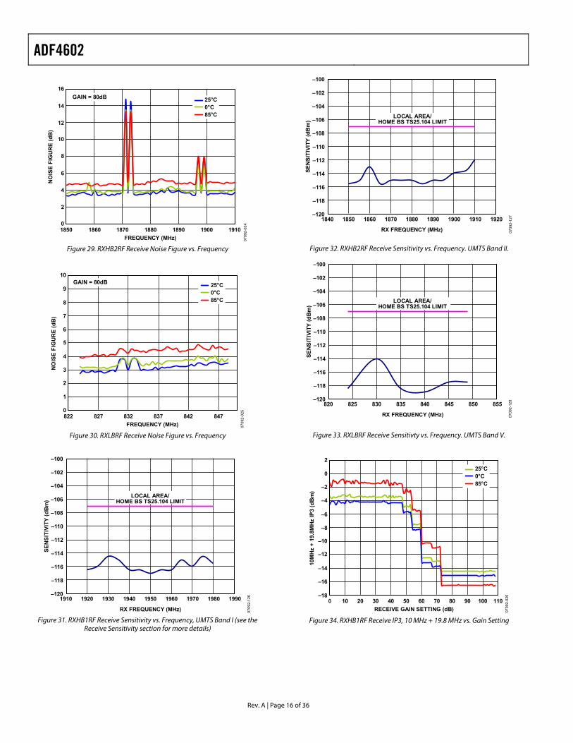
Rev. A | Page 16 of 36
16
14
12
10
8
6
4
2
01850 1860 1870 1880 1890 1900 1910
FREQUENCY (MHz)
NO
ISE
FIG
UR
E (d
B)
0709
2-02
4
25°C0°C85°C
GAIN = 80dB
Figure 29. RXHB2RF Receive Noise Figure vs. Frequency
10
9
8
7
6
5
4
3
2
1
0822 827 832 837 842 847
FREQUENCY (MHz)
NO
ISE
FIG
UR
E (d
B)
0709
2-02
5
25°C0°C85°C
GAIN = 80dB
Figure 30. RXLBRF Receive Noise Figure vs. Frequency
–120
–118
–116
–114
–112
–110
–108
–106
–104
–102
–100
1910 1920 1930 1940 1950 1960 1970 1980 1990
SEN
SITI
VITY
(dB
m)
RX FREQUENCY (MHz)
LOCAL AREA/HOME BS TS25.104 LIMIT
0709
2-12
6
Figure 31. RXHB1RF Receive Sensitivity vs. Frequency, UMTS Band I (see the
Receive Sensitivity section for more details)
–120
–118
–116
–114
–112
–110
–108
–106
–104
–102
–100
1840 1850 1860 1870 1880 1890 1900 1910 1920
SEN
SITI
VITY
(dB
m)
RX FREQUENCY (MHz)
LOCAL AREA/HOME BS TS25.104 LIMIT
0709
2-12
7
Figure 32. RXHB2RF Receive Sensitivity vs. Frequency. UMTS Band II.
–120
–118
–116
–114
–112
–110
–108
–106
–104
–102
–100
820 825 830 835 840 845 850 855
SEN
SITI
VITY
(dB
m)
RX FREQUENCY (MHz)
LOCAL AREA/HOME BS TS25.104 LIMIT
0709
2-12
8
Figure 33. RXLBRF Receive Sensitivty vs. Frequency. UMTS Band V.
–14
–16
–18
–12
–10
–8
–6
–4
–2
0
2
0 10 20 30 40 50 60 70 80 90 100 110RECEIVE GAIN SETTING (dB)
10M
Hz
+ 19
.8M
Hz
IP3
(dB
m)
0709
2-02
6
25°C0°C85°C
Figure 34. RXHB1RF Receive IP3, 10 MHz + 19.8 MHz vs. Gain Setting
ADF4602
Rev. A | Page 17 of 36
–14
–12
–10
–8
–6
–4
–2
0
2
4
6
8
0 10 20 30 40 50 60 70 80 90 100 110RECEIVE GAIN SETTING (dB)
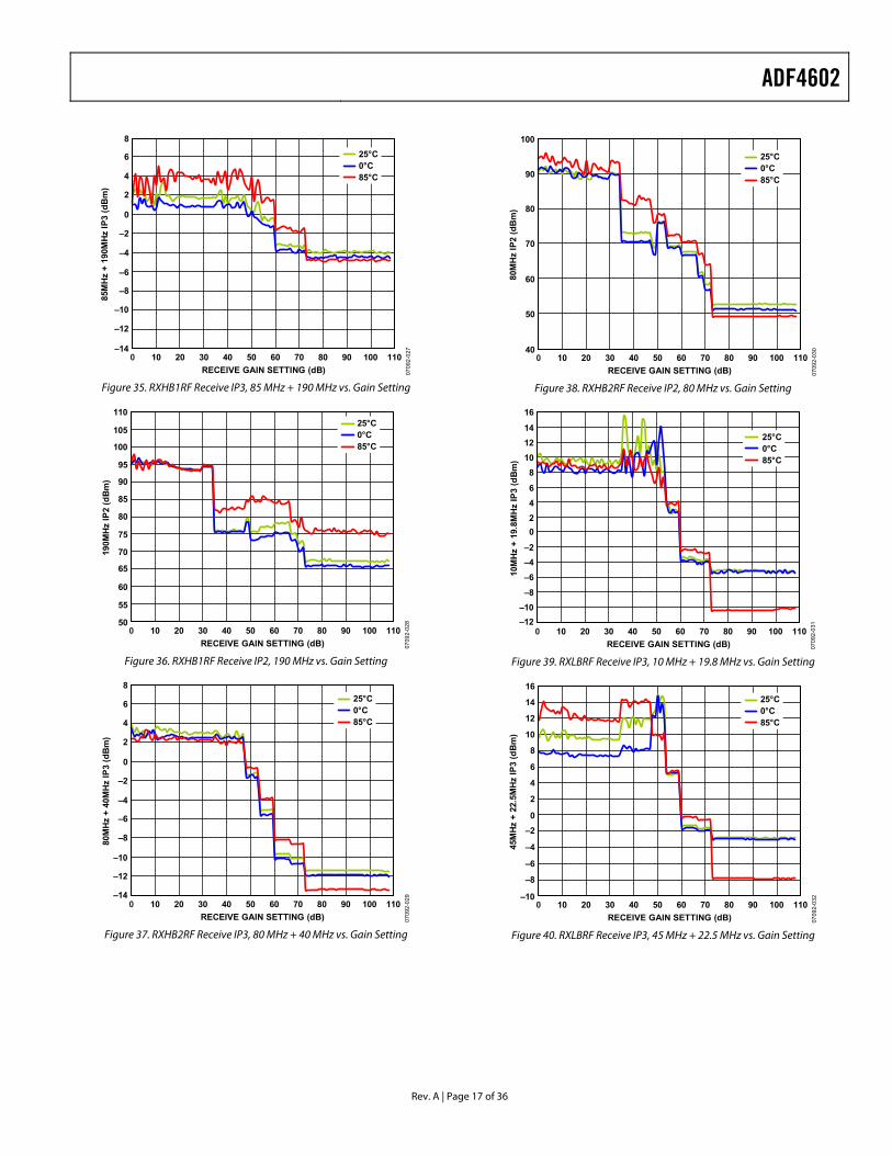
85M
Hz
+ 19
0MH
z IP
3 (d
Bm
)
0709
2-02
7
25°C0°C85°C
Figure 35. RXHB1RF Receive IP3, 85 MHz + 190 MHz vs. Gain Setting
50
55
60
65
70
75
80
85
90
95
100
105
110
0 10 20 30 40 50 60 70 80 90 100 110RECEIVE GAIN SETTING (dB)
190M
Hz
IP2
(dB
m)
0709
2-02
8
25°C0°C85°C
Figure 36. RXHB1RF Receive IP2, 190 MHz vs. Gain Setting
–10
–12
–14
–8
–6
–4
–2
0
2
4
6
8
0 10 20 30 40 50 60 70 80 90 100 110RECEIVE GAIN SETTING (dB)
80M
Hz
+ 40
MH
z IP
3 (d
Bm
)
0709
2-02
9
25°C0°C85°C
Figure 37. RXHB2RF Receive IP3, 80 MHz + 40 MHz vs. Gain Setting
40
50
60
70
80
90
100
0 10 20 30 40 50 60 70 80 90 100 110RECEIVE GAIN SETTING (dB)
80M
Hz
IP2
(dB
m)
0709
2-03
0
25°C0°C85°C
Figure 38. RXHB2RF Receive IP2, 80 MHz vs. Gain Setting
16
141210
8
6420
–2–4–6
–8–10–12
0 10 20 30 40 50 60 70 80 90 100 110RECEIVE GAIN SETTING (dB)
10M
Hz
+ 19
.8M
Hz
IP3
(dB
m)
0709
2-03
1
25°C0°C85°C
Figure 39. RXLBRF Receive IP3, 10 MHz + 19.8 MHz vs. Gain Setting
–10
–8
–6
–4
–20
2
4
6
8
10
12
14
16
0 10 20 30 40 50 60 70 80 90 100 110RECEIVE GAIN SETTING (dB)
45M
Hz
+ 22
.5M
Hz
IP3
(dB
m)
0709
2-03
2
25°C0°C85°C
Figure 40. RXLBRF Receive IP3, 45 MHz + 22.5 MHz vs. Gain Setting

ADF4602
Rev. A | Page 18 of 36
40
30
50
60
70
80
90
100
0 10 20 30 40 50 60 70 80 90 100 110RECEIVE GAIN SETTING (dB)
45M
Hz
IP2
(dB
m)
0709
2-03
3
25°C0°C85°C
Figure 41. RXLBRF Receive IP2, 45 MHz vs. Gain Setting
ADF4602
Rev. A | Page 19 of 36
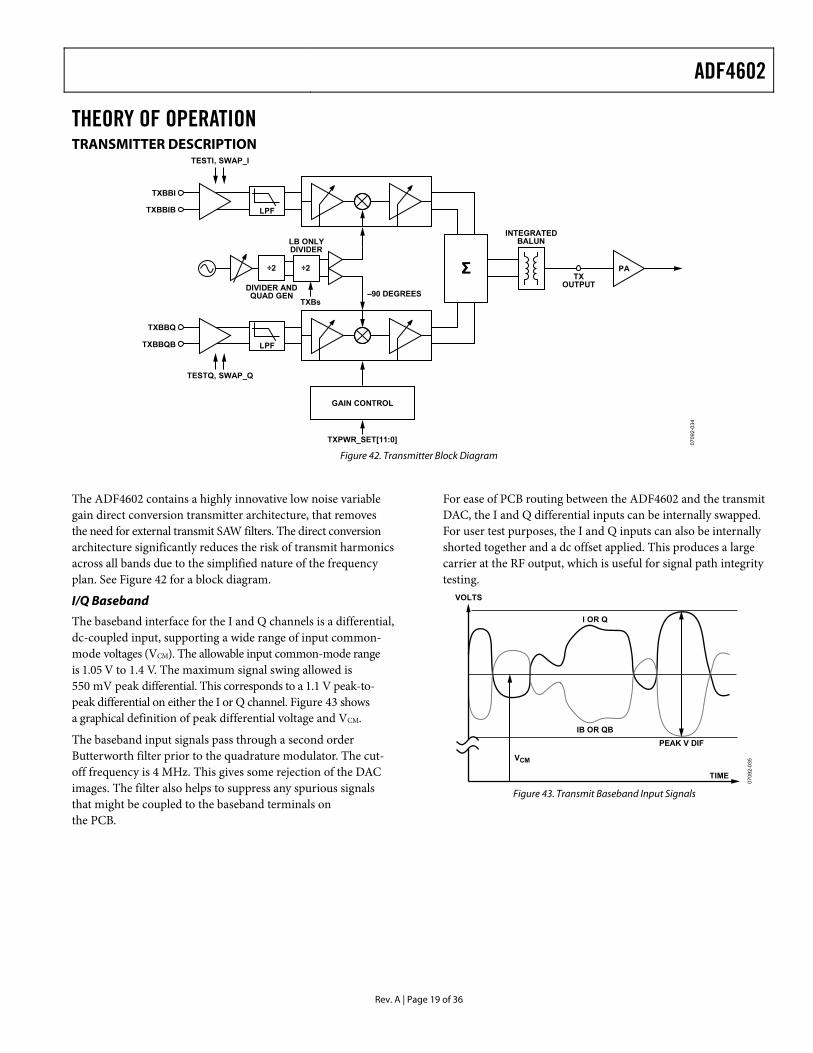
THEORY OF OPERATION TRANSMITTER DESCRIPTION
TXBBI
TXBBIB
TXBBQ
TXBBQB
GAIN CONTROL
TXPWR_SET[11:0]
–90 DEGREES
÷2 ÷2
TXBs
TESTQ, SWAP_Q
TESTI, SWAP_I
Σ
LPF
LPF
PATX
OUTPUT
LB ONLYDIVIDER
DIVIDER ANDQUAD GEN
INTEGRATEDBALUN
0709
2-03
4
Figure 42. Transmitter Block Diagram
The ADF4602 contains a highly innovative low noise variable gain direct conversion transmitter architecture, that removes the need for external transmit SAW filters. The direct conversion architecture significantly reduces the risk of transmit harmonics across all bands due to the simplified nature of the frequency plan. See Figure 42 for a block diagram.
I/Q Baseband
The baseband interface for the I and Q channels is a differential, dc-coupled input, supporting a wide range of input common-mode voltages (VCM). The allowable input common-mode range is 1.05 V to 1.4 V. The maximum signal swing allowed is 550 mV peak differential. This corresponds to a 1.1 V peak-to-peak differential on either the I or Q channel. Figure 43 shows a graphical definition of peak differential voltage and VCM.
The baseband input signals pass through a second order Butterworth filter prior to the quadrature modulator. The cut-off frequency is 4 MHz. This gives some rejection of the DAC images. The filter also helps to suppress any spurious signals that might be coupled to the baseband terminals on the PCB.
For ease of PCB routing between the ADF4602 and the transmit DAC, the I and Q differential inputs can be internally swapped. For user test purposes, the I and Q inputs can also be internally shorted together and a dc offset applied. This produces a large carrier at the RF output, which is useful for signal path integrity testing.
VCM
I OR Q
IB OR QBPEAK V DIF
VOLTS
TIME
0709
2-03
5
Figure 43. Transmit Baseband Input Signals

ADF4602
Rev. A | Page 20 of 36
I/Q Modulator
The I/Q modulator converts the transmit baseband input signals to RF. Calibration techniques are used to maintain accurate IQ balance and phase across frequency and environmental conditions, thus ensuring that 3GPP carrier leakage and EVM and ACLR requirements are met with good margin under all conditions. The on-chip calibrations are carried out during the transmit PLL lock time specified and are self-contained, requiring no additional input from the user.
The modulator has an 80 dB gain control range, programmable in 1/32 of a decibel step. The 12-bit word txpwr_set[11:0] in Register 28 controls the transmit output power. The setting is referenced to a full-scale (500 mV peak differential) sine wave signal applied to the transmit baseband inputs. To calculate the output power when a WCDMA modulated signal with a certain peak-to-average ratio is applied, Equation 1 should be used.
Output Power (dBm/3.84 MHz) = txpwr(dBm) − PAR(dB) (1)
where txpwr(dBm) is the txpwr_set[11:0] value converted to dBm, and PAR is the peak-to-average ratio of the WCDMA signal. For example, if an output power of −8 dBm is required for a WCDMA signal with a peak-to-average ratio of 10 dB
txpwr(dBm) = −8 dBm + 10 dB = +2 dBm
The current consumption of the modulator scales with output power. When the TX power is backed off from maximum, the transceiver benefits from lower power dissipation.
VCO Output
The TX VCO output is fed to a tuned buffer stage and then to the quadrature generation circuitry. The tuned buffer ensures that minimum current and LO related noise is generated in the VCO transport. This action is transparent to the user. The quadrature generator creates the highly accurate phased signals required to drive the modulator and also acts as a divide-by-2. In low band, an additional divide-by-2 is used in the VCO transport path, which is bypassed in high band. This is done to minimize the VCO tuning range required to cover all the bands.
The phase accuracy of the signals is important in ensuring good modulation quality and accurate output power. An on-chip calibration ensures that the phased signals are exactly 90° out of phase. This calibration runs each time the frequency is changed or if the txpwr_set[11:0] word is written to. If the temperature of the device changes, this calibration should be updated. To run the calibration, the user should simply write to the txpwr_set[11:0] word for each five degree change in temperature, or update the value regularly (every few seconds) between WCDMA frames or timeslots. This ensures that good EVM and accurate output power are maintained as the temperature of the device changes.
TX Output Baluns
The baseband input, modulator, and all associated circuitry are fully differential to maintain high signal integrity and noise immunity. However, a differential output is not optimal for the
user because most power amplifiers (PAs) are singled-ended. This situation would normally require additional external matching components or a differential to single-ended SAW filter structure. With the ADF4602, the SAW filter is not necessary, and the required low loss balun is fully integrated, converting the diffe-rential internal signals to a single-ended 50 Ω output, thus allowing easy interfacing to the PA.
The high band output is available at the TXHBRF pin, and the low band output is available at the TXLBRF pin. These are directly connected to a 50 Ω load, if necessary, and do not require ac-coupling.
DACS The ADF4602 integrates two DACs that are designed to interface to an external PA to control reference or bias nodes within the PA. If this function is not required, the DACs are used for any general purpose or powered down if not required.
DAC1 is a 5-bit voltage output DAC. The output range is from 2.3 V to 3.15 V (for VDD > 3.15 V). The DAC1 output stage is supplied directly from VDD, with the capability to supply 10 mA of current to within 50 mV of VDD. For high accuracy, the DAC reference is supplied from LDO5, which is internally trimmed to 25 mV accuracy. The DAC1 output is set by the PADAC1[4:0] word.
DAC2 is a 6-bit voltage output DAC with a range from 0 V to 2.8 V. LDO5 supplies both the reference voltage and full-scale output voltage for DAC2. The output voltage is set by the padac2_ow[5:0] word. The dacgpo_owen bit must also be set high if control of DAC2 is required.
Both DACS are powered down by writing the code, 0x0, to the respective control register.
GENERAL PURPOSE OUTPUTS Four general-purpose outputs (GPOs) are provided on the ADF4602. These are used to control PA bias modes or, more commonly, the GPOs are used to control external RF front-end switches in the transmit/receive path. The GPOs are simple 3 V digital output drivers. GPO1 to GPO3 are capable of supplying a maximum current of 2 mA, whereas GPO4 can supply up to 10 mA.
For operation of the GPOs, Bit dacgpo_owen must be set to 1. The GPOs are then controlled via the gpo_ow[3:0] word.
RECEIVER DESCRIPTION The ADF4602 contains a fully integrated direct conversion receiver designed for multiband WCDMA femtocell applications. High performance, low power consumption, and minimal external components are the key features of the design.
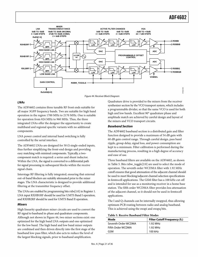
Figure 44 shows a block diagram of the receiver, which consists of three LNA blocks for multiband operation, high linearity I/Q mixers, advanced baseband channel filtering, and a DC offset compensation circuit.
ADF4602
Rev. A | Page 21 of 36
GAIN CONTROL
HIGH BAND LNA 1
HIGH BAND LNA 2
LOW BAND LNA
RxGAIN[6:0]
VCMSEL
RxEN[1:0]
LNA ACTIVE FILTER CHANGESMIXER
TRANSCONDUCTANCE0dB TO 18dB
3 × 6dB STEPS
VGA–6dB TO +18dB24 × 1dB STEPS
0dB TO 18dB3 × 6dB STEPS
0dB TO 18dB3 × 6dB STEPS
18dB TO 30dB (WCDMA)27dB TO 39dB (CDMA)
2 × 6dB STEPS
RXHB2RF
RXBBI
RXBBIB
RXBBQ
RXBBQB
RXHB1RF
RXLBRF
LPF
LPF
BPF
BPF
BPF
DAC
DAC
RXBW_TOGGLE
ADC
ADC
LPF
LPF
LPF
LPF
PROGRAMMABLE OFFSETCONTROL
÷2 OR÷4
0709
2-03
6
Figure 44. Receiver Block Diagram
LNAs
The ADF4602 contains three tunable RF front ends suitable for all major 3GPP frequency bands. Two are suitable for high band operation in the region 1700 MHz to 2170 MHz. One is suitable for operation from 824 MHz to 960 MHz. Thus, the three integrated LNAs offer the designer the opportunity to create multiband and regional specific variants with no additional components.
LNA power control and internal band switching is fully controlled by the serial interface.
The ADF4602 LNAs are designed for 50 Ω single-ended inputs, thus further simplifying the front-end design and providing easy matching with minimal components. Typically, a two-component match is required: a series and shunt inductor. Within the LNA, the signal is converted to a differential path for signal processing in subsequent blocks within the receive signal chain.
Interstage RF filtering is fully integrated, ensuring that external out-of-band blockers are suitably attenuated prior to the mixer stages. The LNA characteristic is designed to provide additional filtering at the transmitter frequency offset.
The LNAs are enabled by programming bits rxbs[1:0] in Register 1. LNA input RXHB1RF should be used for UMTS Band I operation, and RXHB2RF should be used for UMTS Band II operation.
Mixers
High linearity quadrature mixer circuits are used to convert the RF signal to baseband in-phase and quadrature components. Although not shown in Figure 44, two mixer sections exist: one optimized for the high band LNA outputs and one optimized for the low band. The high band and low band mixer outputs are combined and then driven directly into the first stage of the baseband low-pass filter, which also acts to reduce the level of the largest blocking signals, prior to baseband amplification.
Quadrature drive is provided to the mixers from the receiver synthesizer section by the VCO transport system, which includes a programmable divider, so that the same VCO is used for both high and low bands. Excellent 90° quadrature phase and amplitude match are achieved by careful design and layout of the mixers and VCO transport circuits.
Baseband Section
The ADF4602 baseband section is a distributed gain and filter function designed to provide a maximum of 54 dB gain with 60 dB gain control range. Through careful design, pass band ripple, group delay, signal loss, and power consumption are kept to a minimum. Filter calibration is performed during the manufacturing process, resulting in a high degree of accuracy and ease of use.
Three baseband filters are available on the ADF4602, as shown in Table 5. Bits rxbw_toggle[2:0] are used to select the mode of operation. The seventh order WCDMA filter with 1.92 MHz cutoff ensures that good attenuation of the adjacent channel should be used to meet blocking/adjacent channel selection specifications in femtocell applications. The GSM filter has a 100 kHz cut-off and is intended for use as a monitoring receiver in a home base station. The fifth order WCDMA filter provides less attenuation of the adjacent channel, so it should not be used in femtocell applications.
The I and Q channels can be internally swapped, thus allowing optimum PCB routing between radio and analog baseband. This is achieved using the swapi and swapq bits.
Table 5. Receive Baseband Filter Modes Mode Filter Cutoff Frequency (fC) Seventh Order WCDMA 1.92 MHz Fifth Order WCDMA 1.92 MHz GSM 100 kHz
ADF4602
Rev. A | Page 22 of 36
The receive baseband outputs have a programmable common mode voltage of 1.2 V or 1.4 V, selectable via the vcmsel bit in Register 15.
Gain Control
Gain control is distributed throughout the receive signal chain as shown in Figure 46. The RF front end contains 30 dB of control range: 18 dB in the LNA and 12 dB in the mixer transconductance stage. The two baseband active filter stages each provide 18 dB of gain control range in 6 dB steps. Filter characteristics (ripple and group delay) are best conserved if the active filter stages have equal gain. This results in a total of 36 dB gain control in 4× 12 dB steps for the filter stage. The variable gain amplifier (VGA) implements 24 dB of gain controllable in 1 dB steps. The base gain of the mixer is 18 dB, and the base gain of the VGA is −6 dB. This gives a total of 102 dB gain with 90 dB of gain control range.
The base gain of the mixer stage is 18 dB in WCDMA mode and 27 dB in GSM mode.
Table 6. Receive Gain Control in WCDMA mode Stage Gain Control Control Steps LNA 0 dB to +18 dB 3 × 6 dB steps Mixer +18 dB to +30 dB (WCDMA)
+27 dB to +39 dB (GSM) 2 × 6 dB steps
Filter 0 dB to +36 dB 3 × 12 dB steps VGA −6 dB to +18 dB 24 × 1 dB steps
To simplify programming and to ensure optimum receiver performance and dynamic range, the user simply programs the total desired receive gain in dB via the rx_gain[6:0] bits in Register 11. The ADF4602 then decodes the gain setting and automatically distributes the gain between the various blocks. To allow some flexibility, predefined user inputs control the gain threshold points at which the LNA and mixer gain steps occur.
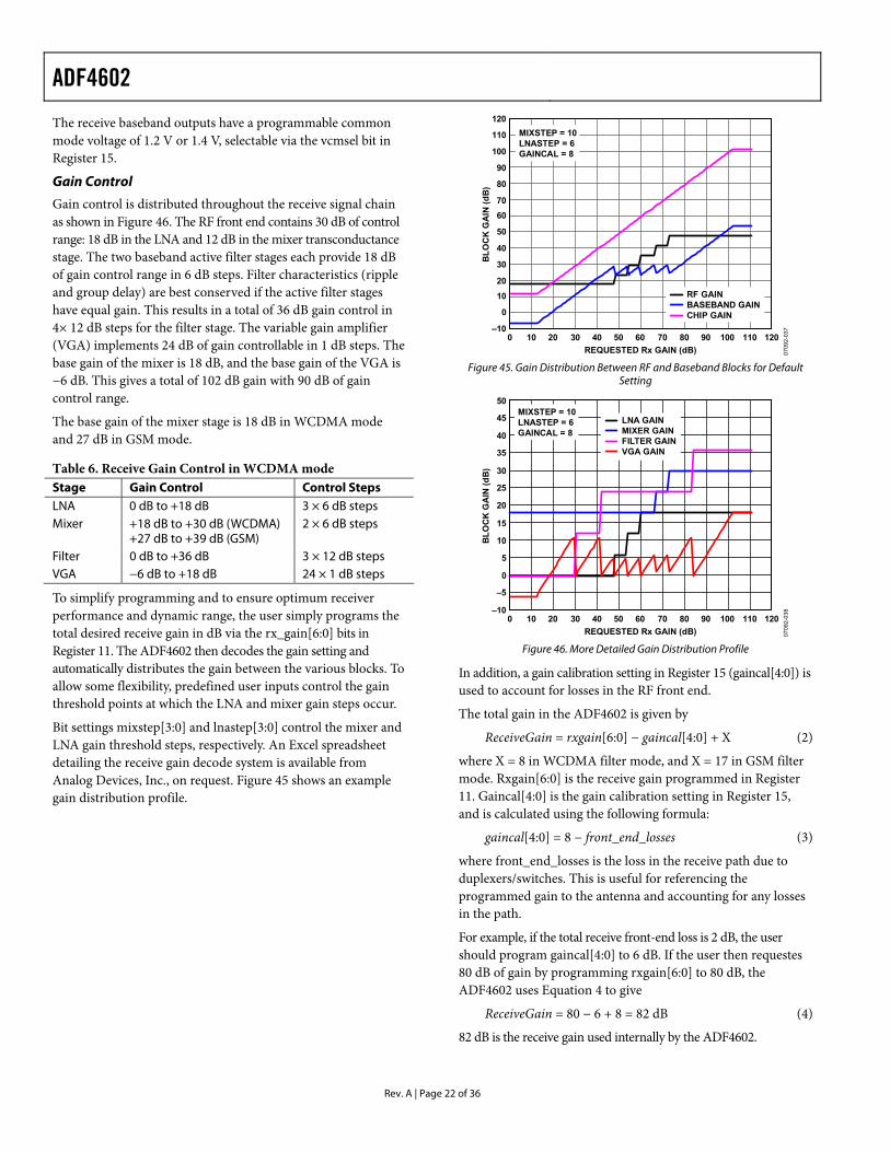
Bit settings mixstep[3:0] and lnastep[3:0] control the mixer and LNA gain threshold steps, respectively. An Excel spreadsheet detailing the receive gain decode system is available from Analog Devices, Inc., on request. Figure 45 shows an example gain distribution profile.
120
110
100
90
80
7060
50
40
30
2010
0
–100 10 20 30 40 50 60 70 80 90 100 110 120
REQUESTED Rx GAIN (dB)
BLO
CK
GA
IN (d
B)
0709
2-03
7
RF GAINBASEBAND GAINCHIP GAIN
MIXSTEP = 10LNASTEP = 6GAINCAL = 8
Figure 45. Gain Distribution Between RF and Baseband Blocks for Default
Setting
50
45
40
35
30
25
20
15
10
5
0
–5
–100 10 20 30 40 50 60 70 80 90 100 110 120
REQUESTED Rx GAIN (dB)
BLO
CK
GA
IN (d
B)
0709
2-03
8
LNA GAINMIXER GAINFILTER GAINVGA GAIN
MIXSTEP = 10LNASTEP = 6GAINCAL = 8
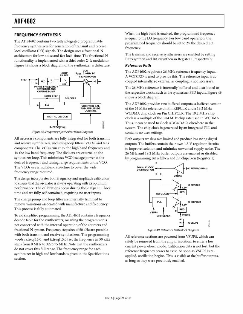
Figure 46. More Detailed Gain Distribution Profile
In addition, a gain calibration setting in Register 15 (gaincal[4:0]) is used to account for losses in the RF front end.
The total gain in the ADF4602 is given by
ReceiveGain = rxgain[6:0] − gaincal[4:0] + X (2)
where X = 8 in WCDMA filter mode, and X = 17 in GSM filter mode. Rxgain[6:0] is the receive gain programmed in Register 11. Gaincal[4:0] is the gain calibration setting in Register 15, and is calculated using the following formula:
gaincal[4:0] = 8 − front_end_losses (3)
where front_end_losses is the loss in the receive path due to duplexers/switches. This is useful for referencing the programmed gain to the antenna and accounting for any losses in the path.
For example, if the total receive front-end loss is 2 dB, the user should program gaincal[4:0] to 6 dB. If the user then requestes 80 dB of gain by programming rxgain[6:0] to 80 dB, the ADF4602 uses Equation 4 to give
ReceiveGain = 80 − 6 + 8 = 82 dB (4)
82 dB is the receive gain used internally by the ADF4602.

ADF4602
Rev. A | Page 23 of 36
DC Offset Compensation
Due to the very high proportion of the total system gain assigned to the analog baseband function, compensating for dc offsets is an inherent part of any direct conversion solution. DC offsets are characterized as falling into two categories: static or slow varying and time varying
The ADF4602 architecture has been designed to reduce the amount of time varying dc offsets. The device also includes a dc offset control system. The control system consists of ADCs at the baseband output to digitize dc offsets: a digital signal processing block where the characteristics of the loop are programmed for customization of the loops transfer function, and trim DACs that are used to introduce the error term back into the signal path. The offset control transfer function can either be programmed to act as a servo loop that is automatically triggered by a gain change or as a high-pass filter (HPF) with an automatic fast settling mode that is also triggered by a gain change. Parameters of the servo loop, high-pass filter, and fast settling mode are set by the initial ADF4602 programming. In operation, the dc offset control system is fully automatic and does not require any external programming. Recommended default programming conditions for the dc offset compensation loop are shown in the Register Description section.
POWER MANAGEMENT The ADF4602 contains integrated power management requiring two external power supplies: 3.3 V VDD and 1.8 V VINT. Figure 47 shows a block diagram.
VDD supplies the five integrated low drop-out regulators (LDOs), VSUP1 to VSUP5, that are used to supply the vast majority of the internal circuitry. VSUP6, VSUP7, and VSUP8 supply the receive PLL, transmit PLL, and reference block, respectively. These nodes require external connections to ensure good supply isolation and ensure a minimum level of interference between the PLL/reference blocks and the rest of the transceiver. VSUP6 and VSUP7 should be connected to VSUP3, whereas VSUP8 should be connected to VSUP2.
Each node, VSUP1 to VSUP8, should be externally decoupled to ground with a 0.1 μF capacitor. Y5V capacitors are not recommended for use here. X7R, X5R, C0G, or a similar type of capacitor should be used.
C1
C3
C4
RX VCO RX LNAs TX VCO1.8V 2.8V
1.9V
C6 C7
REF PATHREF OP
(SER INTREAD)
TX MODTX BB
PWR DETDACs
RXBASEBAND
ANDMIXERS RX PLL TX PLL
VSUP8VSUP7VSUP6VSUP5VSUP4VSUP3VSUP2VSUP1VBATVINT
C2 C5ANALOG BBOR VSUP2
DIGITAL 1.8VSUPPLY
SERIALINTERFACE
LDO1
LDO2
LDO3
LDO4
LDO5
0709
2-03
9
Figure 47. Power Management Block
VINT supplies the serial interface enabling register data preservation with minimum current consumption during power-down. This should be supplied with 1.8 V externally.
The five LDOs are individually powered up/down via bits ldoen[4:0] in Register 1. Table 7 summarizes the supply strategy.
Note that the reference path (VSUP8) supply is supplied from an external source or the internal VSUP2. The external supply option may be convenient so that the entire reference path can be shut down by collapsing a single supply.
VSUP8 can also be programmed to supply the voltage used for serial interface readback. See the Serial Port Interface (SPI) section for more information.
Table 7. Power Management Strategy Pin Connection Usage Volts VINT External Serial interface control
logic 1.8 V
VDD External Main device supply, DAC1
3.3 V
VSUP1 Internal LDO1 Receive VCO 2.6 V VSUP2 Internal LDO2 Receive baseband and
down-converter 2.8 V
VSUP3 Internal LDO3 Receive LNAs 1.9 V VSUP4 Internal LDO4 Transmit VCO 2.6 V VSUP5 Internal LDO5 Transmit baseband,
modulator, DAC2, and GPOs
2.8 V
VSUP6 Connect to VSUP3 Receive synthesizer 1.9 V VSUP7 Connect to VSUP3 Transmit synthesizer 1.9 V VSUP8 VSUP2 or external Reference path,
reference buffer outputs; Optional: serial interface readback
2.8 V
ADF4602
Rev. A | Page 24 of 36
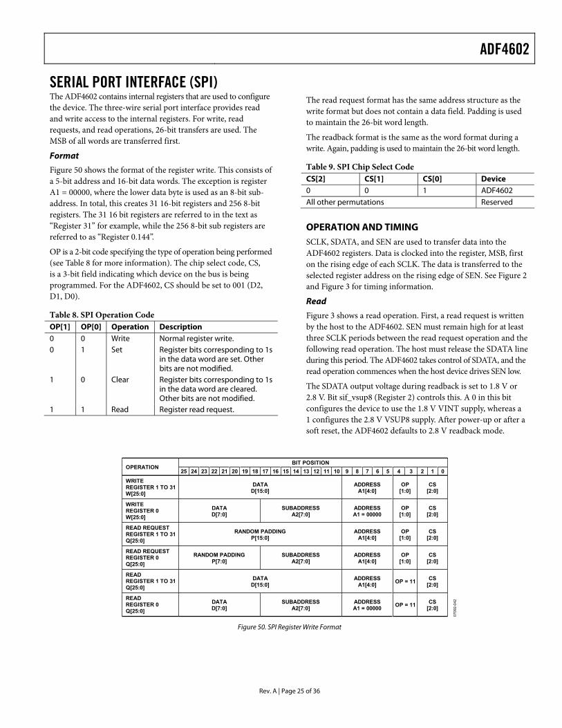
FREQUENCY SYNTHESIS The ADF4602 contains two fully integrated programmable frequency synthesizers for generation of transmit and receive local oscillator (LO) signals. The design uses a fractional-N architecture for low noise and fast lock-time. The fractional-N functionality is implemented with a third
order Σ-Δ modulator.
Figure 48 shows a block diagram of the synthesizer architecture.
PFDFREF
LOOPFILTER
CP
DIVIDERS
DIGITAL DECODE
RxFREQ[15:0]
50kHz STEP
÷2LPF
VCOFVCO: 3.4GHz TO
4.4GHz RANGE
VCO FREQ CALAND AMPLITUDE
CONTROL
Σ-∆
PHASE FREQUENCYDETECTOR ANDCHARGE PUMP
0709
2-04
0
Figure 48. Frequency Synthesizer Block Diagram
All necessary components are fully integrated for both transmit and receive synthesizers, including loop filters, VCOs, and tank components. The VCOs run at 2× the high band frequency and 4× the low band frequency. The dividers are external to the synthesizer loop. This minimizes VCO leakage power at the desired frequency and tuning range requirements of the VCO. The VCOs use a multiband structure to cover the wide frequency range required.
The design incorporates both frequency and amplitude calibration to ensure that the oscillator is always operating with its optimum performance. The calibrations occur during the 200 μs PLL lock time and are fully self contained, requiring no user inputs.
The charge pump and loop filter are internally trimmed to remove variations associated with manufacture and frequency. This process is fully automated.
To aid simplified programming, the ADF4602 contains a frequency decode table for the synthesizers, meaning the programmer is not concerned with the internal operation of the counters and fractional-N system. Frequency step sizes of 50 kHz are possible with both transmit and receive synthesizers. The programming words rxfreq[15:0] and txfreq[15:0] set the frequency in 50 kHz steps from 0 MHz to 3276.75 MHz. Note that the synthesizers do not cover this full range. The frequency range for each synthesizer in high and low bands is given in the Specifications section.
When the high band is enabled, the programmed frequency is equal to the LO frequency. For low band operation, the programmed frequency should be set to 2× the desired LO frequency.
The transmit and receive synthesizers are enabled by setting Bit txsynthen and Bit rxsynthen in Register 1, respectively.
Reference Path
The ADF4602 requires a 26 MHz reference frequency input. A VCTCXO is used to provide this. The reference input is ac-coupled internally, so external ac coupling is not necessary.
The 26 MHz reference is internally buffered and distributed to the respective blocks, such as the synthesizer PFD inputs. Figure 49 shows a block diagram.
The ADF4602 provides two buffered outputs: a buffered version of the 26 MHz reference on Pin REFCLK and a 19.2 MHz WCDMA chip clock on Pin CHIPCLK. The 19.2 MHz chip clock is a multiple of the 3.84 MHz chip rate used in WCDMA. Thus, it can be used to clock ADCs/DACs elsewhere in the system. The chip clock is generated by an integrated PLL and contains no user settings.
Both outputs are slew rate limited and produce low swing digital outputs. The buffers contain their own 1.5 V regulator circuits to improve isolation and minimize unwanted supply noise. The 26 MHz and 19.2 MHz buffer outputs are enabled or disabled by programming Bit refclken and Bit chipclken (Register 1).
PLL
REFIN (26MHz)
REFCLK
CHIPCLK
VSUP8
VSUP8
VSUP8
VSUP8
REG
REG
1.5V
1.5V
CHIPCLKEN
REFCLKEN
26MHz CLOCKDISTRIBUTION
0709
2-04
1
Figure 49. Reference Path Block Diagram
All reference sections are powered from VSUP8, which can safely be removed from the chip in isolation, to enter a low current power-down mode. Calibration data is not lost, but the reference frequency ceases to exist. As soon as VSUP8 is re-applied, oscillation begins. This is visible at the buffer outputs, as long as they were previously enabled.
ADF4602
Rev. A | Page 25 of 36
SERIAL PORT INTERFACE (SPI) The ADF4602 contains internal registers that are used to configure the device. The three-wire serial port interface provides read and write access to the internal registers. For write, read requests, and read operations, 26-bit transfers are used. The MSB of all words are transferred first.
The read request format has the same address structure as the write format but does not contain a data field. Padding is used to maintain the 26-bit word length.
The readback format is the same as the word format during a write. Again, padding is used to maintain the 26-bit word length.
Format Table 9. SPI Chip Select Code Figure 50 shows the format of the register write. This consists of
a 5-bit address and 16-bit data words. The exception is register A1 = 00000, where the lower data byte is used as an 8-bit sub-address. In total, this creates 31 16-bit registers and 256 8-bit registers. The 31 16 bit registers are referred to in the text as “Register 31” for example, while the 256 8-bit sub registers are referred to as “Register 0.144”.
CS[2] CS[1] CS[0] Device 0 0 1 ADF4602 All other permutations Reserved
OPERATION AND TIMING SCLK, SDATA, and SEN are used to transfer data into the ADF4602 registers. Data is clocked into the register, MSB, first on the rising edge of each SCLK. The data is transferred to the selected register address on the rising edge of SEN. See Figure 2 and Figure 3 for timing information.
OP is a 2-bit code specifying the type of operation being performed (see Table 8 for more information). The chip select code, CS, is a 3-bit field indicating which device on the bus is being programmed. For the ADF4602, CS should be set to 001 (D2, D1, D0). Read
Table 8. SPI Operation Code Figure 3 shows a read operation. First, a read request is written by the host to the ADF4602. SEN must remain high for at least three SCLK periods between the read request operation and the following read operation. The host must release the SDATA line during this period. The ADF4602 takes control of SDATA, and the read operation commences when the host device drives SEN low.
OP[1] OP[0] Operation Description 0 0 Write Normal register write. 0 1 Set Register bits corresponding to 1s
in the data word are set. Other bits are not modified.
1 0 Clear Register bits corresponding to 1s in the data word are cleared. Other bits are not modified.
1 1 Read Register read request.
The SDATA output voltage during readback is set to 1.8 V or 2.8 V. Bit sif_vsup8 (Register 2) controls this. A 0 in this bit configures the device to use the 1.8 V VINT supply, whereas a 1 configures the 2.8 V VSUP8 supply. After power-up or after a soft reset, the ADF4602 defaults to 2.8 V readback mode.
BIT POSITIONOPERATION
25 24 23 22 21 20 19 18 17 16 15 14 13 12 11 10 9 8 7 6 5 4 3 2 1 0WRITEREGISTER 1 TO 31W[25:0]
WRITEREGISTER 0W[25:0]
READ REQUESTREGISTER 1 TO 31Q[25:0]
READ REQUESTREGISTER 0Q[25:0]
READREGISTER 1 TO 31Q[25:0]
READREGISTER 0Q[25:0]
DATAD[15:0]
RANDOM PADDINGP[15:0]
DATAD[7:0]
SUBADDRESSA2[7:0]
RANDOM PADDINGP[7:0]
SUBADDRESSA2[7:0]
DATAD[7:0]
SUBADDRESSA2[7:0]
DATAD[15:0]
ADDRESSA1[4:0]
ADDRESSA1 = 00000
ADDRESSA1[4:0]
ADDRESSA1[4:0]
ADDRESSA1 = 00000
ADDRESSA1[4:0]
OP[1:0]
OP[1:0]
OP[1:0]
OP = 11
OP = 11
OP[1:0]
CS[2:0]
CS[2:0]
CS[2:0]
CS[2:0]
CS[2:0]
CS[2:0]
0709
2-04
2
Figure 50. SPI Register Write Format

ADF4602
Rev. A | Page 26 of 36
REGISTERS REGISTER MAP
A1
1
2
W0x2FFDrxsynthen
reset_soft
sif_vsup8
txsynthen
chipclken
refclken rxbs[1:0]txbstxenldoen[4:0]rxen
W0x0002
D15 D14 D13 D12 D11 D10 D9 D8 D7 D6 D5 D3D4 D2 D1 D0 DEFAULT1 R/W
A1
10
11
12
13
14
15
W
W
W
W
W
W
0x9858rxfreq[15:0]
0x0000rxgain[6:0]
0x0FA6
0x103E
0xEE53
lnastep[3:0]
nper0[3:0]
nint0[3:0]
mixstep[3:0]
nper1[3:0]
nint1[3:0]
sdmen[3:0]
nper2[3:0]
nint2[3:0]
rfskip[3:0]
osadc2x[3:0]
nint3[3:0]
0x0890sdmosrgaincal[4:0]rxbw[2:0]swapiswapqvcmsel
D15 D14 D13 D12 D11 D10 D9 D8 D7 D6 D5 D3D4 D2 D1 D0 DEFAULT1 R/W
A1
21
22
26
28
31
31
W
W
W
W
W
0x001Fvcm_sat_thres[5:0]cmmodtest_Q/swap_Qtest_I/swap_I gain_blanksel[1:0]
0x8000padac1[4:0]padac2_ow[5:0]gpo_ow[3:0]dacgpo_owen
0x0000txfreq[15:0]
0x0001txpwr_set[11:0] cntrl_mode
0x0000nvmld
Rrevid[7:0]
D15 D14 D13 D12 D11 D10 D9 D8 D7 D6 D5 D3D4 D2 D1 D0 DEFAULT1 R/W
SUB-ADDRESS REGISTERS
TRANSMITTER USER REGISTERS
RECEIVER USER REGISTERS
GENERAL USER REGISTERS
A1 A2
0 144
0 151
0 153
0 155
0 165
0 170
W
W
W
W
W
W
0x06reserved[1:0]
0x6F
0x85
0x78
0x20
vsup2[7:0]
reserved[7:0]
reserved[7:0]
reserved[7:0]
0xF0en_mix[3:0]
D7 D6 D5 D3D4 D2 D1 D0 DEFAULT1 R/W
0709
2-04
3
NOTES1THESE ARE RECOMMENDED DEFAULT SETTINGS THAT SHOULD BE PROGRAMMED INTO THE REGISTERS.
0x0021
Figure 51. Register Map
ADF4602
Rev. A | Page 27 of 36
REGISTER DESCRIPTION
Table 10. General User Registers Register Bit Bit Name Description
13 rxen Set this bit high to enable the receiver. A low here disables the receiver. 1, A1, Write 12 refclken Setting this bit high enables the 26 MHz reference output buffer. 11 chipclken Setting this bit high enables the19.2 MHz chip clock output buffer. [10:6] ldoen The on-chip LDOs are powered down individually. For normal operation all LDOs should be enabled
(Bits[10 : 6] = [11111]) ldoen[10:6]1 Mode XXXX1 VSUP1 2.6 V enable XXX1X VSUP2 2.8 V enable XX1XX VSUP3 1.8 V enable X1XXX VSUP4 2.6 V enable 1XXXX VSUP5 2.8 V enable 5 txen Setting this bit high enables the transmitter. 4 txbs This bit controls which of the transmit outputs is in use. 0 = low band (TXLBRF), 1 = high band (TXHBRF). 3 txsynthen Setting this bit high enables the transmit synthesizer. [2:1] rxbs These bits control the receiver band select. rxbs[2:1] Operation 00 Reserved 01 Low band enable (RXLBRF) 10 High Band 1 enable (RXHB1RF) (default) 11 High Band 2 enable (RXHB2RF) 0 rxsynthen Setting this bit high enables the receive synthesizer 2, A1, Write
1 sif_vsup8 The serial port readback (SDATA) output voltage is changed from 1.8 V to 2.8 V with this bit. 0 = use 1.8 V VINT supply, 1 = use 2.8 V VSUP8 supply. After power-up or after a soft reset, the ADF4602 defaults to 2.8 V readback mode.
0 reset_soft A rising edge on this bit starts a 50 μs reset pulse for the full chip. This bit is self clearing. It is recommended that a soft reset be performed after power-up.
1 X = don’t care.

ADF4602
Rev. A | Page 28 of 36
Table 11. Receiver User Registers Register Bit Bit
Name Description
10, A1, Write
[15:0] rxfreq These bits set the receive synthesizer frequency in 50 kHz steps from 0 MHz to 3276.75 MHz. For the high bands this is equal to the channel frequency, and for the low bands it is 2× the channel frequency. For example:
Bit 15 to Bit 0 (Hex)
RXHB1RF, RXHB2RF Synthesizer Frequency RXLBRF Synthesizer Frequency
0x9470 1900 MHz 950 MHz 0x9858 1950 MHz 975 MHz
[6:0] rxgain These bits set the receiver gain in conjunction with the gaincal[4:0] setting in register 15. LSB = 1 dB. 11, A1, Write 0x00 = 0dB, 0x7F = 127 dB. Gain = rxgain − gaincal + X where X is 8 in WCDMA mode and 17 in GSM mode. The mode is selected by the rxbw bits in
Register 15. With mixstep = 6 and lnastep = 10, the valid range for rxgain is from 12 dB to 102 dB. Settings outside of
these are clipped at 12 dB and 102 dB. See Figure 45 for an example. [15:12] rfskip Skip offset control state when no RF gain step occurred for State 3 to State 0. Default = 0x0 = 0. 12, A1,
Write [11:8] sdmen Σ-Δ modulator enable for State 3 to State 0. Default = 0xF = 15. [7:4] mixstep Gain decode threshold for mixer gain reduction step. LSB = 4 dB steps. Default = 0xA = 10. [3:0] lnastep Gain decode threshold for LNA gain reduction step. LSB = 4 dB steps. Default = 0x6 = 6.
[15:12] osadc2x Offset measurement ADC range for State 3 to State 0. Default = 0x1 = 1. 13, A1, Write [11:8] nper2 State duration for State 2. Default = 0x0 = 0. [7:4] nper1 State duration for State 1. Default = 0x3 = 3. [3:0] nper0 State duration for State 0. Default = 0xE = 14.
[15:12] nint3 Integrator time constant for State 3. Default = 0xE = 14. 14, A1, Write [11:8] nint2 Integrator time constant for State 2. Default =0xE = 14. [7:4] nint1 Integrator time constant for State 1. Default = 0x5 = 5. [3:0] nint0 Integrator time constant for State 0. Default = 0x3 = 3.
11 vcmsel This sets the receive baseband output common-mode voltage. 0 = 1.2 V, 1 = 1.4 V. 15, A1, Write 10 swapq Setting this bit high swaps the differential Q outputs, RXBBQ and RXBBQB. 9 swapi Setting this bit high swaps the differential I outputs, RXBBI and RXBBIB. [8:6] rxbw This bit controls the receive baseband filter bandwidth.
rxbw [8:6] Filter Mode 000 Fifth order WCDMA filter (not recommended for femtocells) 010 Seventh order WCDMA filter (recommended WCDMA filter for
femtocells) 111 GSM filter
Else Reserved [5:1] gaincal These bits are used for calibration of front-end loss. LSB = 1 dB, 0x00 = 0 dB, 0x1F = 31 dB. It is used in the
calculation of the receive gain. See rxgain in Register 11. If not used for calibration, this should be set to 8 in WCDMA mode and 17 in GSM mode.
0 sdmosr Offset loop Σ-Δ modulator over sampling ratio. 1 = 4×, 0 = 2× (default)

ADF4602
Rev. A | Page 29 of 36
Table 12. Transmitter User Registers Register Bit Bit Name Description
[12:11] test_I/swap_I These bits allow various options on the I inputs as detailed in the following table: 21, A1, Write Bits Function 00 Normal operation 01 Swap I differential inputs for ease of PCB routing to DAC 10 Zero input on I inputs 11 DC offset applied to I inputs; creates large carrier at RF [10:9] test_Q/swap_Q These bits allow various options on the Q inputs as detailed in the table below: Bits Function 00 Normal operation 01 Swap Q differential inputs for ease of PCB routing to DAC 10 Zero input on Q inputs 11 DC offset applied to Q inputs: creates large carrier at RF [8:7] gain_blanksel During a transmit gain change, some spectral splatter may occur at the output of the transmitter.
These bits allow the input baseband signal at the input to the low-pass filter to be blanked for a short period, to reduce the spectral splatter observed during the gain change.
gain_blanksel[8:7] Operation 00 Default setting; no blanking 01 230 ns blanking 10 540 ns blanking 11 850 ns blanking 6 cmmod This bit adjusts the internal modulator common-mode setting. It should be set to 0. Setting this bit
to 1 results in reduced power consumption but degrades transmit linearity. [5:0] vcm_sat_thres This bit should be set to 0x1F for normal operation.
15: dacgpo_owen Setting this bit high allows the user to have manual control over DAC2 and GPO1 to GPO4. 22, A1, Write [14:11] gpo_ow These bits allow manual control of GPO 1 to GPO 4. Bit dacgpo_owen must be set to 1 to allow this
mode of operation. Each bit controls one of the GPOs as per the following table. This allows all possible permutations of GPO output combinations.
gpo_ow[14 :11]1 Mode XXX1 GPO1 high XX1X GPO2 high X1XX GPO3 high 1XXX GPO4 high [10:5] padac2_ow These bits allow manual control of DAC2. Bit dacgpo_owen must be set to 1 to allow this mode of
operation. [4:0] padac1 These bits control DAC1. 26, A1, Write
[15:0] txfreq These bits set the transmitter synthesizer frequency in 50 kHz steps from 0 MHz to 3276.75 MHz. For the high bands, this is equal to the channel frequency, and for the low bands it is 2× the channel frequency. For example:
Bit 15 to Bit 0 (Hex) HB Synthesizer Frequency LB synthesizer Frequency 0xA730 2140 MHz 1070 MHz 0xA988 2170 MHz 1085 MHz

ADF4602
Rev. A | Page 30 of 36
Register Bit Bit Name Description 28, A1 Write
[15:4] txpwr_set Requested transmit power at antenna. LSB = 1/32 dBm, 0x000 = −80 dBm, 0xFFF = 47.96875 dBm. The output power is referenced to a full scale sine wave applied to the transmit baseband inputs. For WCDMA modulated signals, the output power measured in a 3.84 MHz bandwidth is reduced by the peak to average ratio of the signal. See the I/Q Modulator section for more details. The valid range of transmit output power setting is −80 dBm to +10 dBm. Output clipping may occur sooner, depending on the PAR of the applied signal. The txpwr_set register should be updated periodically, or with every 5°C change in temperature to ensure accurate output power. See the VCO Output section for more details.
0 Set this bit to 1 to control the output power from the txpwr_set bits. 31, A1 Write
4 nvmld Setting this bit to 1 triggers a manual load of the nonvolatile memory contents. See the Software Initialization Procedure section for more details.
31, A1 Read
[7:0] revid Chip Revision ID. Revision represented in hex value. A readback of 0x21 represents Rev 2.1.
1 X = don’t care.
Table 13. Sub-Address Registers Register Bit Bit Name Description 0.144, A2 Write [2:1] reserved[1:0] These bits should be set to 11 for normal operation. 0.151, A2 Write [7:0] vsup2[7:0] These bits control the VSUP2 regulator voltage and should be set to 0x6F for normal
operation. During the initialization sequence, the VSUP2 voltage is temporarily set to 3.1 V. See the Software Initialization Procedure section for more details.
0.153, A2 Write [7:0] reserved[7:0] These bits should be set to 0x85 for normal operation. 0.155, A2 Write [7:0] reserved[7:0] These bits should be set to 0x78 for normal operation. 0.165, A2 Write [7:0] reserved[7:0] These bits should be set to 0x20 for normal operation. 0.170, A2 Write [7:4] en_mix[3:0] These bits enable the I, IB, Q, and QB channels of the modulator separately. Set these bits
to all 1s to enable the modulator for normal operation.

ADF4602
Rev. A | Page 31 of 36
SOFTWARE INITIALIZATION PROCEDURE INITIALIZATION SEQUENCE Table 14 shows the initialization sequence that should be used after power-up. Note that the 26 MHz reference clock must be applied to the REFIN pin before programming begins. The default settings are described in the comments section, and some settings, such as output frequency, gain, and GPO settings, may vary from those required in the end application of the user. The user can substitute his own settings in these instances.
Table 14. Initialization Sequence Step Register1 Data Comment 1 02 0x0003 Performs a soft reset of the ADF4602. The reset takes 50 μs, and no registers should be written to during this
period. After 50 μs, programming can continue as normal. This bit is self clearing. If using 1.8 V logic levels, this register should be programmed to 0x0001 instead of 0x0003.
2 0.151 0xE0 Set VSUP2 to 3.1 V. See the Nonvolatile Memory (NVM) Initialization section for more details. 3 31 0x0010 Transfers non-volatile memory (NVM) contents to registers. Wait 200 μs before next programming step. 4 31 0x0000 Negate bit set in last programming step. 5 0.151 0x6F Set VSUP2 back to 2.8 V. 6 01 0x2FDD Enables receiver and disables transmit output. Selects TXHBRF pin as the transmit output and RXHB1RF as
the receive input. Enables all on-chip regulators. 19.2 MHz output clock is enabled, 26 MHz output clock is disabled. If it is desired to disable the 19.2 MHz output clock, this register is programmed to 0x27DD.
7 12 0x0FA6 Default settings for mixer and LNA gain reduction steps. 8 13 0x103E Default settings. 9 14 0xEE53 Default settings. 10 15 0x0890 Sets received gain calibration, WCDMA filter mode, and output common-mode voltage to 1.4 V. 11 21 0x001F Default settings. 12 22 0x8000 Enables DAC and GPO manual control. 13 0.144 0x06 Default settings. 14 0.155 0x78 Default settings. 15 0.153 0x85 Default settings. 16 0.165 0x20 Default settings. 17 0.170 0xF0 Default settings. 18 11 0x0050 Receiver gain set to 80 dB. 19 10 0x9858 Receiver synthesizer frequency set to 1950 MHz. The PLL takes 200 μs to lock. Registers should not be
written to during this period. 20 26 0xA730 Transmit synthesizer frequency set to 2140 MHz. The PLL takes 200 μs to lock. Registers should not be
written to during this period. 21 01 0x2FFD Enables transmit output. 22 28 0xA001 Enables control of the output power and sets the txpwr_set field to 0 dBm. Control of output power is via
the txpwr_set bits. 1 Register numbers 0.xxx are 8-bit registers as described in the SPI Interface section of the ADF4602-x data sheet.

ADF4602
Rev. A | Page 32 of 36
Nonvolatile Memory (NVM) Initialization
The ADF4602 has on-chip non-volatile memory (NVM) that contains chip factory calibration coefficients. A soft reset of the device transfers the contents of NVM to internal registers; however, this has been found to be unreliable if performed at temperatures below 0°C. The software work-around outlined in Step 2 to Step 5 of Table 14 ensures that the NVM data is transferred reliably under all operating conditions. It involves setting the VSUP2 on-chip regulator to 3.1 V, manually transferring the data by setting the nvmld bit in Register 31, and then resetting the VSUP2 regulator to 2.8 V. Device programming can then continue as normal.
Programming Transmit and Receive frequencies
After initialization, the transmit/receive synthesizer frequencies may need to be changed. To change the transmit frequency, write the new frequency word to Register 26. When a new transmit frequency is programmed, the transmit output power is auto-
matically turned off to prevent any unwanted transmissions as the PLL locks. The user should wait 200 μs (time taken for PLL to lock), and then set the output power to the desired value by writing to Register 28.
If the user disables the transmit synthesizer, the transmit output power must be turned off before reenabling the transmit synthesizer. This is achieved by two means: setting Bit D5 in Register 1 or setting the output power in Register 28 to a minimum.
After reenabling the synthesizer, and then locking the synthesizer to a frequency by programming the frequency word in Register 26, the user can reenable the output power.
To change the receive frequency, simply program the new frequency in Register 10, and wait 200 μs before using the device as a transceiver. The receive gain is set at any time (apart from during the 200 μs PLL locking transient).

ADF4602
Rev. A | Page 33 of 36
APPLICATIONS INFORMATION INTERFACING THE ADF4602 TO THE AD9963 AD9963 ADC Inputs
The AD9963 Rx path analog inputs have a nominal differential impedance of 4 kΩ. The nominal dc bias level of the inputs is 1.4 V. An internal differential voltage reference creates positive and negative reference voltages that define the full-scale input voltage of the ADCs.
This full-scale input voltage range can be adjusted by means of the RX_FSADJ[4:0] parameter in Configuration Register 0x7D. RX_FSADJ should be set to 0x1F for default operation with the ADF4602. This sets the peak-to-peak input voltage range to the midrange value of 1.54 V.
Interfacing to the AD9963 Rx Baseband Inputs
The ADF4602 baseband outputs have a nominal output common-mode voltage that can be set to 1.4 V. The ADF4602 can be dc-coupled to the AD9963. It is recommended that a first-order low-pass filter be placed between the two devices to reject unwanted high frequency signals that may alias into the desired baseband signal.
100Ω
100Ω
68pF
68pF
ADCAD9963
ADF4602
RXIP
RXIN
RXBBI
RXBBIB
0880
1-11
8
Figure 52. ADF4602 to AD9963 Receive Interface Circuit
In this configuration, the ADF4602 is setting the common-mode input voltage of the AD9963 ADCs to 1.4 V. The input common-mode buffer of the AD9963 should be disabled (set Register 0x7E, Bit 1 = 1) to avoid contention with the ADF4602 output driver.
AD9963 DAC Outputs
The AD9963 DAC contains a current source array capable of providing a nominal full-scale current (IOUTFS) of 2 mA. DAC full-scale output current is regulated by the reference control amplifier and is determined by the product of a reference current, a programmable reference resistor, RREF, an internal programmable resistor, RSET, and a pair of programmable gain scaling parameters.
Reference Voltage
There is a single reference voltage that is used by both the I and Q channel DACs. The AD9963 REFIO reference voltage is generated by an internal 100 μA current source terminated into
a programmable resistor, RREF. The resistance can be varied by adjusting the REFIO_ADJ[5:0] bits in Register 0x6E, if necessary. For default operation, REFIO_ADJ should be set to zero. This nominal RREF resistance is 10 kΩ resulting in a 1.0 V reference voltage. The AD9963 REFIO pin should be decoupled to AGND with a 0.1 μF capacitor.
Current Scaling Resistor, RSET
Each transmit DAC has a resistor that is used to adjust the full-scale current. The nominal resistance is 16 kΩ, which results in a full-scale current of 2 mA (when VREFIO equals 1.0 V). The 6-bit programmable values, IRSET[5:0] and QRSET[5:0] (Register 0x6A and Register 0x6D) should be set to zero for this default operation.
Gain Scaling Parameters
Each transmit DAC has coarse and fine gain control parameters for scaling the full-scale output currents. These adjustments change only the full-scale current of the DAC and have no impact on the REFIO voltage.
The coarse scale adjust (GAIN1) allows the nominal output current to be changed by ±6 dB in approximately 0.25 dB steps. The adjustment range of the fine scale adjust (GAIN2) is about ±2.5%. These settings can be found in the 0x68, 0x69, 0x6B, and 0x6C registers and in bits five to zero. GAIN1 should be set to 0x01 and GAIN2 should be set to zero for default operation.
RECEIVE SENSITIVITY Figure 31 shows the ADF4602 receive sensitivity vs. frequency for UMTS Band I using the RXHB1RF input port. The sensitivity degradation due to the 63rd and 64th harmonics of the 30.72 MHz ADC sampling frequency can be seen near 1935 MHz and 1966 MHz. The sensitivity degradation caused by these harmonics was minimized by placing 100 Ω series resistors and 68 pF filtering capacitors at the ADC inputs (see Figure 52). Note the sensitivity degradation due to the 76th frequency harmonic of the 26 MHz reference at 1976 MHz. The degra-ation in sensitivity is less than 3 dB for these harmonics.
Overall, the solution exceeds the 3GPP sensitivity specifications by 7 dB across the frequency range. In addition, note that the 100 F capacitors to ground at the AD9963 DAC outputs will minimize sensitivity degradation due to DAC clock harmonics, particularly in UMTS sniff mode.

ADF4602
Rev. A | Page 34 of 36
Interfacing to the AD9963 TX Baseband Outputs
The ADF4602 transmit baseband inputs accept a 1.2 V common-mode input signal with 1 V p-p differential swing. The configu-ration in Figure 53 is used to provide this from the AD9963 TxDACs.
The AD9963 can be dc coupled to the ADF4602 as shown in Figure 53. When configured for a 2 mA full-scale current, the output swing of the circuit is 1 V p-pd. centered at 1.2 V. The AD9963 TXMCL pin is biased at 0.5 V to increase the headroom of the DAC outputs. The AD9963 TXVDD and CLK33V supplies must be supplied with 3.3 V to support this output compliance range from the DACs.
The optional 100 kΩ resistors connected between the AUXIO pins and the TXIN (and TXQN) pins allow a dc offset to be provided to null out carrier leakage at the ADF4602 outputs. 07
092-
129
226Ω
249Ω 0.1uF
249Ω
249Ω
100kΩ
226Ω
249Ω
249Ω
249Ω
100kΩ
TXIN
TXIP
TXCML
AUXIO2
TXQN
AUXIO3
TXQP
TXBBQB
TXBBQ
TXBBI
TXBBIB
AD9963ADF4602
100pF
100pF
100pF
100pF
Figure 53. AD9963 to ADF4602 Tx Interface Circuitry
.

ADF4602
Rev. A | Page 35 of 36
OUTLINE DIMENSIONS
140
1011
3130
2120
4.254.10 SQ3.95
TOPVIEW
6.00BSC SQ
PIN 1INDICATOR
5.75BSC SQ
12° MAX
0.300.230.18
0.20 REFSEATINGPLANE
1.000.850.80
0.05 MAX0.02 NOM
COPLANARITY0.08
0.80 MAX0.65 TYP
4.50REF
0.500.400.30
0.50BSC
PIN 1INDICATOR
0.60 MAX0.60 MAX
0.25 MIN
EXPOSEDPAD
(BOT TOM VIEW)
COMPLIANT TO JEDEC STANDARDS MO-220-VJJD-2 0721
08-A
FOR PROPER CONNECTION OFTHE EXPOSED PAD, REFER TOTHE PIN CONFIGURATION ANDFUNCTION DESCRIPTIONSSECTION OF THIS DATA SHEET.
Figure 54. 40-Lead Lead Frame Chip Scale Package [LFCSP_VQ]
6 mm × 6 mm Body, Very Thin Quad (CP-40-1)
Dimensions shown in millimeters
ORDERING GUIDE Model1 Temperature Range Package Description Package Option ADF4602BCPZ 0°C to +85°C 40-Lead Lead Frame Chip Scale Package [LFCSP_VQ] CP-40-1 ADF4602BCPZ-RL 0°C to +85°C 40-Lead Lead Frame Chip Scale Package [LFCSP_VQ] CP-40-1 EV-ADF4602EB3ZTST Baseband Adapter Board EVAL-ADF4602EB3Z UMTS Band I Femtocell Base Station Evaluation Board. Includes
UMTS Mode.
EVAL-ADF4602EB5Z UMTS Band II/Band V Femtocell Base Station Evaluation Board. Includes UMTS Mode.
1 Z = RoHS Compliant Part.

ADF4602
Rev. A | Page 36 of 36
NOTES
©2009–2011 Analog Devices, Inc. All rights reserved. Trademarks and registered trademarks are the property of their respective owners. D07092-0-2/11(A)