Embed Size (px)
Citation preview

Shuji Nakamura, Ph.D. Professor of Materials Department
University of California, Santa Barbara Santa Barbara, CA 93106-5050
EDUCATION
1994 University of Tokushima, Japan Doctor of Engineering
1979 University of Tokushima, Japan Master of Electronic Engineering
1977 University of Tokushima, Japan Bachelor of Electronic Engineering
ACADEMIC APPOINTMENTS
1999 – Present University of California, Santa Barbara Professor, Materials Department
1993 – 1999 Nichia Chemical Ind., Ltd. Senior Researcher, Department of Research and Development (R&D)
1989 – 1993 Nichia Chemical Ind., Ltd. Group Head, Research and Development 2nd Section
1988 – 1989 University of Florida Visiting Research Associate, Electronic Engineering
1985 – 1988 Nichia Chemical Ind., Ltd. Group Head, Research and Development 1st Section
1979 – 1984 Nichia Chemical Ind., Ltd. Research and Development
HONORS & AWARDS
1994, 1996 Nikkei BP Engineering Award
1994, 1997 Best Paper Award of Japanese Applied Physics Society
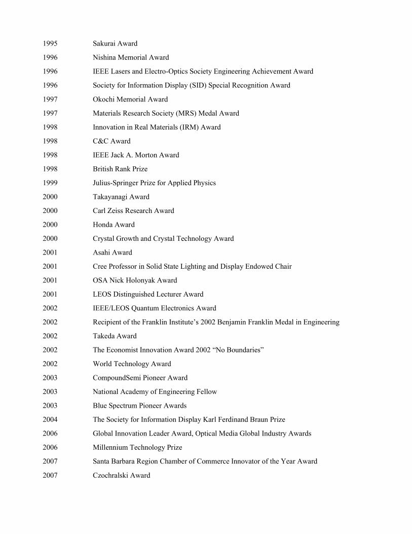
1995 Sakurai Award
1996 Nishina Memorial Award
1996 IEEE Lasers and Electro-Optics Society Engineering Achievement Award
1996 Society for Information Display (SID) Special Recognition Award
1997 Okochi Memorial Award
1997 Materials Research Society (MRS) Medal Award
1998 Innovation in Real Materials (IRM) Award
1998 C&C Award
1998 IEEE Jack A. Morton Award
1998 British Rank Prize
1999 Julius-Springer Prize for Applied Physics
2000 Takayanagi Award
2000 Carl Zeiss Research Award
2000 Honda Award
2000 Crystal Growth and Crystal Technology Award
2001 Asahi Award
2001 Cree Professor in Solid State Lighting and Display Endowed Chair
2001 OSA Nick Holonyak Award
2001 LEOS Distinguished Lecturer Award
2002 IEEE/LEOS Quantum Electronics Award
2002 Recipient of the Franklin Institute’s 2002 Benjamin Franklin Medal in Engineering
2002 Takeda Award
2002 The Economist Innovation Award 2002 “No Boundaries”
2002 World Technology Award
2003 CompoundSemi Pioneer Award
2003 National Academy of Engineering Fellow
2003 Blue Spectrum Pioneer Awards
2004 The Society for Information Display Karl Ferdinand Braun Prize
2006 Global Innovation Leader Award, Optical Media Global Industry Awards
2006 Millennium Technology Prize
2007 Santa Barbara Region Chamber of Commerce Innovator of the Year Award
2007 Czochralski Award

2008 Japanese Science of Applied Physics (JSAP) Outstanding Paper Award for the “Demonstration of Nonpolar m-Plane InGaN/GaN Laser Diode”
2008 The Prince of Asturias Award for Technical Scientific Research (The Prince of Asturias Foundation)
2009 Harvey Prize
2011 2012 2013
Technology and Engineering Emmy Award Inventor of the Year Award by Silicon Valley Intellectual Property Law Association LED Pioneer Awards
2013 LUX Awards “LUX person of the Year in association with One-LUX”
2013 Awards of Outstanding Achievement for Global SSL Development by ISA (International SSL Alliances)
2014 Nobel Prize in Physics
2014 Order of Culture Award, Japan
2014 National Academy of Inventors (NAI) Member
2014 Goleta’s Finest – Special Recognition by the Goleta Chamber of Commerce
2015 Charles Stark Draper Prize for Engineering
2015 National Academy of Inventors Fellow
2015 Japanese Science of Applied Physics (JSAP) Honorary Member
2015 National Inventors Hall of Fame
2015 Physical Society of Japan Honorary Member
2015 Pioneer Award, 21st annual South Coast Business & Technology Awards
2015 Global Energy Prize
2015 Asia Game Changer
2015 Eagle on the World
2015 Japanese Illuminating Engineering Institute Honorary Member
2015 Japanese Institute of Electronics and information Honorary Member
2015 Japanese Institute of Electrical and Electronic Engineering Honorary Member
2015 AAEOY Distinguished Science and Technology Award in Los Angeles
2015 Doctor Honoris Cause from Wroclaw University in Poland
2016 The Asian Award/Outstanding Achievement in Science & Technology, London, England
2016 The Nelson W. Taylor Keynote Award, The Pennsylvania State University
2016 Asian & Pacific Islander American (APIA) Heritage Award, Sacramento, CA
2016 Ordine dei Santi Mauizio e Lazzaro
2017 Academia Sinica Fellow, Taiwan

2017 Mountbatten Medal Achievement Award, Institute of Engineering and Technology, England
2017 Asia Pacific Brands Foundation Awards: Legendary Award
2017 Doctor Honoris Causa from University of Warsaw in Poland
2017 Honorary Fellowship Awards from Hong Kong Baptist University ACKM
2017 Doctor Honoris Causa from Universidad International Menendez Pelayo in Spain
2018 Zayed Future Energy Prize Lifetime Achievement, United Arab Emirates
2018 Honorary Doctorate Degree from University of Massachusetts Lowell
2018 10th Iwaki Award in Japan
2018 Degree of Doctor of Science in Engineering (Honoris cause) for distinction in engineering from Queen’s University Belfast
2019 Honorary Doctorate of Science, Universiti Sains Malaysia
2020 National Academy of Science (NAS) Award for the Industrial Application of Science PROFESSIONAL ACTIVITIES
1995 Developed the first group-III nitride-based blue/green LEDs
1995 Developed the first group-III nitride-based violet laser diodes (LDs)
1998 – 2000 Editorial Board, Applied Physics Society
2000 – 2007 Research Director, Solid State Lighting and Display Center, UCSB
2007 – 2013 Research Director, Solid State Lighting and Energy Center, UCSB
2014 – Present Research Director, Solid State Lighting and Energy Electronics Center, UCSB
2000 – Present Editorial Board, Compound Semiconductor Magazine
2001 – Present Editor, Materials Research Society Conference Proceedings
2001 – 2007 Director, Exploratory Research for Advanced Technology (ERATO), UCSB
2002 – Present Guest Professor, Shinshu University (Japan)
2004 – Present Guest Professor, Tottori University (Japan)
2004 – Present Honorary Professor, Universtät Bremen (Germany)
2004 – Present Guest Professor, University of Tokushima (Japan)
2005 – 10/2020 Honorary Professor, Wuhan University (China)
2007 – 10/2020 Visiting Honorary Professor, Hong Kong University of Science & Technology
2008 – Present Honorary Graduates: Doctor of Engineering honoris causa, Hong Kong University of Science and Technology
2007 – Present Guest Professor, University of Ehime (Japan)
2009 – 10/2020 Advisor, Shanghai Research Center of Engineering and Technology for Solid-State Lighting (China)

2009 – 10/2020 Advisory Professor, Fudan University (China)
2015 – Present Distinguished Professor, Tokyo University of Agriculture and Technology(Japan)
2015 Doctor Honoris Causa, University of Wroclaw, Poland
2016 University of Michigan Dow Lectureship
2016 GLOBALFOUNDRIES Fab8
2016 Honorary Degree, McGill University, Montreal, Canada
2016 Cohen Distinguished Lecturer, Northwestern University
2016 Gurevitch Lecture, Portland State University, OR
2016 Keynote, International Conference on Physics, New Orleans, LA
2016 Keynote, ICEM2016 Conference, Singapore
2016 Keynote, 2016 QMS symposium, NY
2016 2016 CPS (Chinese Physical Society), Beijing University of Technology, China
2016 LpS 2016 venue, St. Petersburg, Russia
2016 DLS, University of Wisconsin-La Crosse
2016 CeOPP (Center of Optoelectronics and Photonics Paderborn), University of Paderborn, Germany
2016 Nelson W. Taylor Lecturer at Penn State’s University Park
2016 Honorary Professor of China University of Mining and Technology
2017 Honorary Academician, Academia Sinica, Taiwan
2017 Doctorado Honoris Causa, Universidad Internacional Menéndez Pelayo (UIMP), Spain
2017 Honorary Fellowship Awards from Hong Kong Baptist University ACKM
2017 The Doctorate Honoris, University of Warsaw (Poland)
2017 Invited Speaker, Military University of Technology (aka Wojskowa Akademia Techniczna), Warsaw, Poland
2018 Honorary Degree, University of Massachusetts Lowell
2019 Leigh Ann Conn Prize for Renewable Energy
2019 Honorary Degree of Doctor of Science from the Universiti Sains Malaysia
2019 2019 Consumer Technology (CT) Hall of Fame
2019 Royal Academy of Engineering Member
2020 National Academy of Science (NAS) Award for the Industrial Application of Science
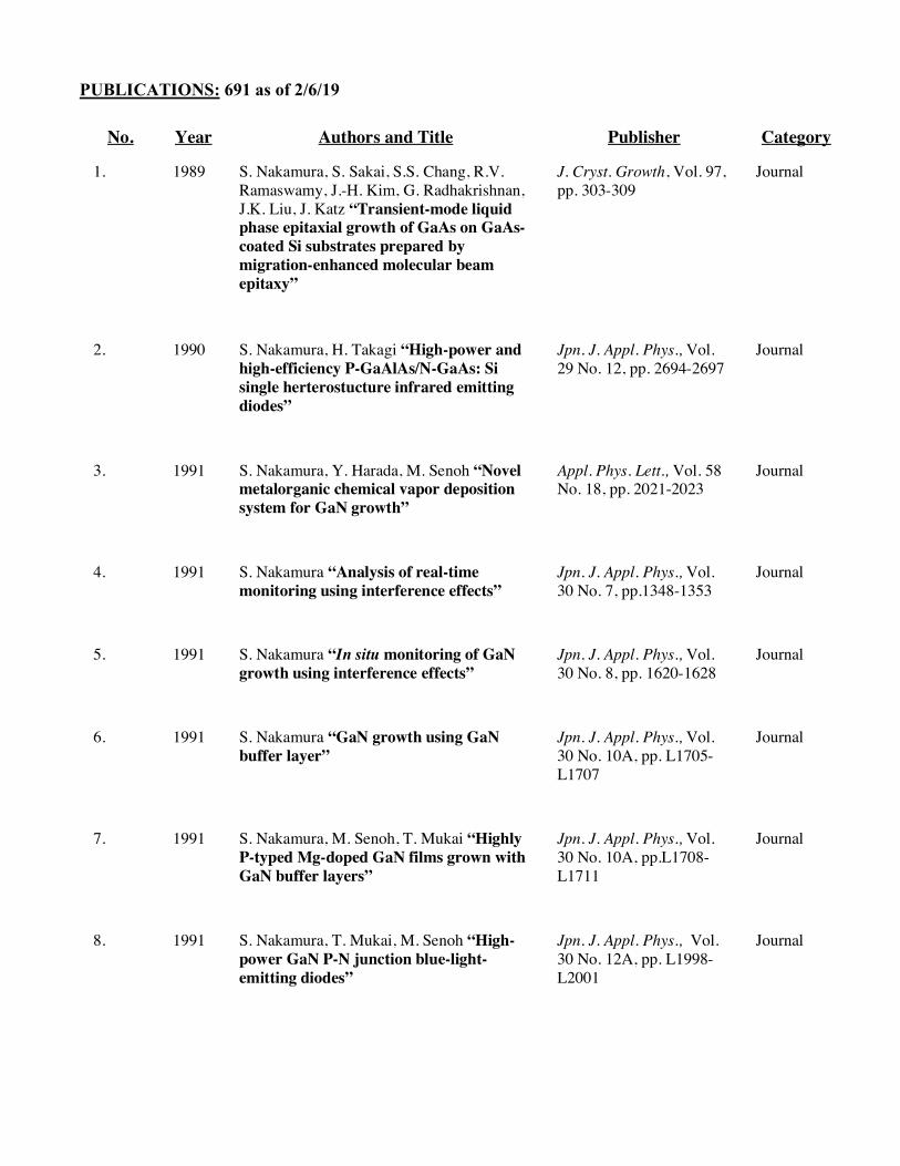
PUBLICATIONS: 691 as of 2/6/19
No. Year Authors and Title Publisher Category
1. 1989 S. Nakamura, S. Sakai, S.S. Chang, R.V. Ramaswamy, J.-H. Kim, G. Radhakrishnan, J.K. Liu, J. Katz “Transient-mode liquid phase epitaxial growth of GaAs on GaAs-coated Si substrates prepared by migration-enhanced molecular beam epitaxy”
J. Cryst. Growth, Vol. 97, pp. 303-309
Journal
2. 1990 S. Nakamura, H. Takagi “High-power and high-efficiency P-GaAlAs/N-GaAs: Si single herterostucture infrared emitting diodes”
Jpn. J. Appl. Phys., Vol. 29 No. 12, pp. 2694-2697
Journal
3. 1991 S. Nakamura, Y. Harada, M. Senoh “Novel metalorganic chemical vapor deposition system for GaN growth”
Appl. Phys. Lett., Vol. 58 No. 18, pp. 2021-2023
Journal
4. 1991 S. Nakamura “Analysis of real-time monitoring using interference effects”
Jpn. J. Appl. Phys., Vol. 30 No. 7, pp.1348-1353
Journal
5. 1991 S. Nakamura “In situ monitoring of GaN growth using interference effects”
Jpn. J. Appl. Phys., Vol. 30 No. 8, pp. 1620-1628
Journal
6. 1991 S. Nakamura “GaN growth using GaN buffer layer”
Jpn. J. Appl. Phys., Vol. 30 No. 10A, pp. L1705-L1707
Journal
7. 1991 S. Nakamura, M. Senoh, T. Mukai “Highly P-typed Mg-doped GaN films grown with GaN buffer layers”
Jpn. J. Appl. Phys., Vol. 30 No. 10A, pp.L1708-L1711
Journal
8. 1991 S. Nakamura, T. Mukai, M. Senoh “High-power GaN P-N junction blue-light-emitting diodes”
Jpn. J. Appl. Phys., Vol. 30 No. 12A, pp. L1998-L2001
Journal

9. 1992 S. Nakamura, T. Mukai, M. Senoh, N. Iwasa “Thermal annealing effects on P-type Mg-doped GaN films”
Jpn. J. Appl. Phys., Vol. 31 No. 2B, pp. L139-L142
Journal
10. 1992 S. Nakamura, N. Iwasa, M. Senoh, T. Mukai “Hole compensation mechanism of P-type GaN films”
Jpn. J. Appl. Phys., Vol. 31 No. 5A, pp. 1258-1266
Journal
11. 1992 S. Nakamura, T. Mukai, M. Senoh “In situ monitoring and hall measurements of GaN growth with GaN buffer layers”
J. Appl. Phys., Vol. 71, No. 11, pp. 5543-5549
Journal
12. 1992 S. Nakamura, T. Mukai, M. Senoh “Si- and Ge-doped GaN films grown with GaN buffer layers”
Jpn. J. Appl. Phys., Vol. 31 No. 9A, pp. 2883-2888
Journal
13. 1992 S. Nakamura, T. Mukai “High-quality InGaN films grown on GaN films”
Jpn. J. Appl. Phys., Vol. 31 No. 10B, pp. L1457-L1459
Journal
14. 1993 S. Nakamura, M. Senoh, T. Mukai “p-GaN/N-InGaN/N-GaN double-heterostructure blue-light-emitting diodes”
Jpn. J. Appl. Phys., Vol. 32 No. 1A/B. pp. L8-L11
Journal
15. 1993 S. Nakamura, T. Mukai, M. Senoh “Si-doped InGaN films grown on GaN films”
Jpn. J. Appl. Phys., Vol. 32 No. 1A/B, pp. L16-L19
Journal
16. 1993 S. Nakamura, N. Iwasa, S. Nagahama “Cd-doped InGaN films grown on GaN films”
Jpn. J. Appl. Phys., Vol. 32 No. 3A, pp. L338-L341
Journal
17. 1993 S. Nakamura, M. Senoh, T. Mukai “High-power InGaN/GaN double-heterostructure violet light-emitting diodes”
Appl. Phys. Lett., Vol. 62 No. 19, pp. 2390-2392
Journal
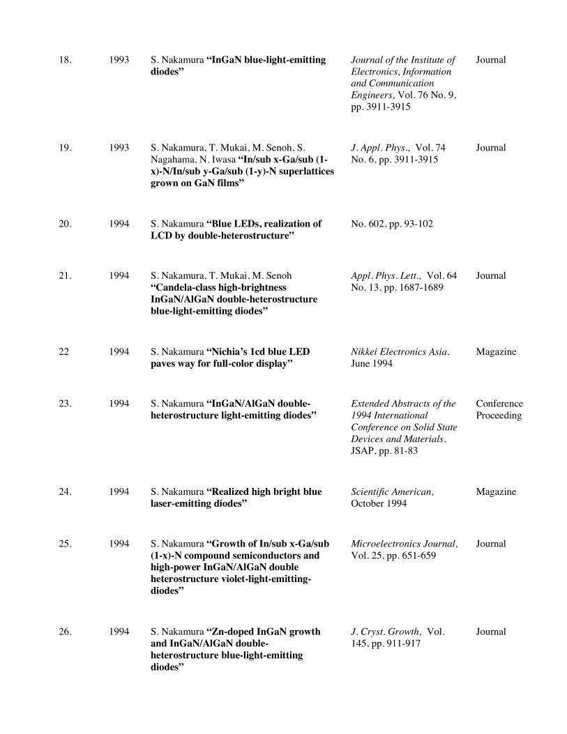
18. 1993 S. Nakamura “InGaN blue-light-emitting diodes”
Journal of the Institute of Electronics, Information and Communication Engineers, Vol. 76 No. 9, pp. 3911-3915
Journal
19. 1993 S. Nakamura, T. Mukai, M. Senoh, S. Nagahama, N. Iwasa “In/sub x-Ga/sub (1-x)-N/In/sub y-Ga/sub (1-y)-N superlattices grown on GaN films”
J. Appl. Phys., Vol. 74 No. 6, pp. 3911-3915
Journal
20. 1994 S. Nakamura “Blue LEDs, realization of LCD by double-heterostructure”
No. 602, pp. 93-102
21. 1994 S. Nakamura, T. Mukai, M. Senoh “Candela-class high-brightness InGaN/AlGaN double-heterostructure blue-light-emitting diodes”
Appl. Phys. Lett., Vol. 64 No. 13, pp. 1687-1689
Journal
22 1994 S. Nakamura “Nichia’s 1cd blue LED paves way for full-color display”
Nikkei Electronics Asia, June 1994
Magazine
23. 1994 S. Nakamura “InGaN/AlGaN double-heterostructure light-emitting diodes”
Extended Abstracts of the 1994 International Conference on Solid State Devices and Materials, JSAP, pp. 81-83
Conference Proceeding
24. 1994 S. Nakamura “Realized high bright blue laser-emitting diodes”
Scientific American, October 1994
Magazine
25. 1994 S. Nakamura “Growth of In/sub x-Ga/sub (1-x)-N compound semiconductors and high-power InGaN/AlGaN double heterostructure violet-light-emitting-diodes”
Microelectronics Journal, Vol. 25, pp. 651-659
Journal
26. 1994 S. Nakamura “Zn-doped InGaN growth and InGaN/AlGaN double-heterostructure blue-light-emitting diodes”
J. Cryst. Growth, Vol. 145, pp. 911-917
Journal
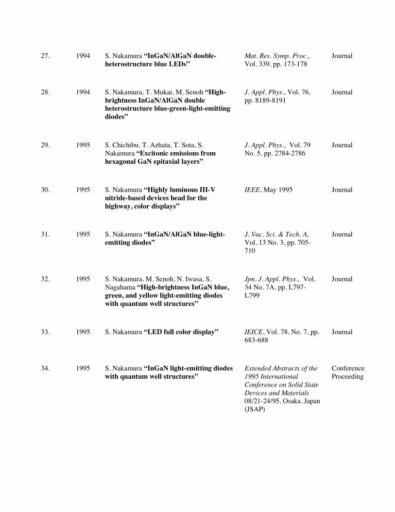
27. 1994 S. Nakamura “InGaN/AlGaN double-heterostructure blue LEDs”
Mat. Res. Symp. Proc., Vol. 339, pp. 173-178
Journal
28. 1994 S. Nakamura, T. Mukai, M. Senoh “High-brightness InGaN/AlGaN double heterostructure blue-green-light-emitting diodes”
J. Appl. Phys., Vol. 76, pp. 8189-8191
Journal
29. 1995 S. Chichibu, T. Azhata, T. Sota, S. Nakamura “Excitonic emissions from hexagonal GaN epitaxial layers”
J. Appl. Phys., Vol. 79 No. 5, pp. 2784-2786
Journal
30. 1995 S. Nakamura “Highly luminous III-V nitride-based devices head for the highway, color displays”
IEEE, May 1995 Journal
31. 1995 S. Nakamura “InGaN/AlGaN blue-light-emitting diodes”
J. Vac. Sci. & Tech. A, Vol. 13 No. 3, pp. 705-710
Journal
32. 1995 S. Nakamura, M. Senoh, N. Iwasa, S. Nagahama “High-brightness InGaN blue, green, and yellow light-emitting diodes with quantum well structures”
Jpn. J. Appl. Phys., Vol. 34 No. 7A, pp. L797-L799
Journal
33. 1995 S. Nakamura “LED full color display” IEICE, Vol. 78, No. 7, pp. 683-688
Journal
34. 1995 S. Nakamura “InGaN light-emitting diodes with quantum well structures”
Extended Abstracts of the 1995 International Conference on Solid State Devices and Materials 08/21-24/95, Osaka, Japan (JSAP)
Conference Proceeding
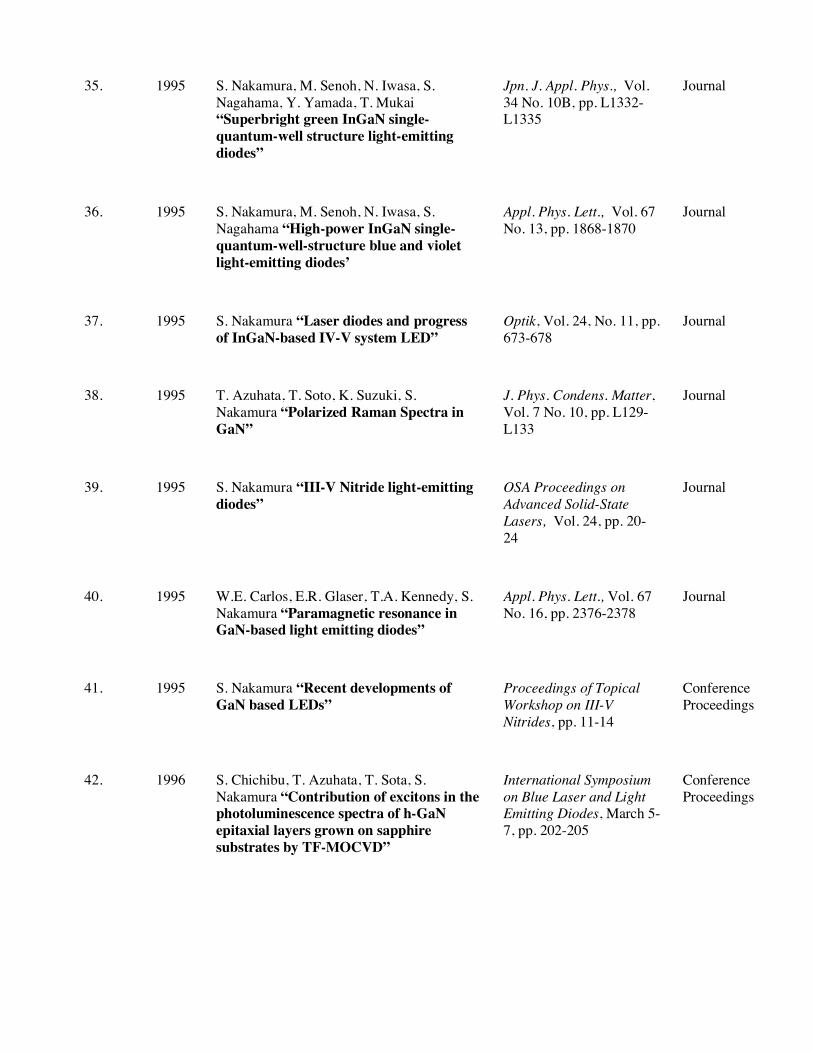
35. 1995 S. Nakamura, M. Senoh, N. Iwasa, S. Nagahama, Y. Yamada, T. Mukai “Superbright green InGaN single-quantum-well structure light-emitting diodes”
Jpn. J. Appl. Phys., Vol. 34 No. 10B, pp. L1332-L1335
Journal
36. 1995 S. Nakamura, M. Senoh, N. Iwasa, S. Nagahama “High-power InGaN single-quantum-well-structure blue and violet light-emitting diodes’
Appl. Phys. Lett., Vol. 67 No. 13, pp. 1868-1870
Journal
37. 1995 S. Nakamura “Laser diodes and progress of InGaN-based IV-V system LED”
Optik, Vol. 24, No. 11, pp. 673-678
Journal
38. 1995 T. Azuhata, T. Soto, K. Suzuki, S. Nakamura “Polarized Raman Spectra in GaN”
J. Phys. Condens. Matter, Vol. 7 No. 10, pp. L129-L133
Journal
39. 1995 S. Nakamura “III-V Nitride light-emitting diodes”
OSA Proceedings on Advanced Solid-State Lasers, Vol. 24, pp. 20-24
Journal
40. 1995 W.E. Carlos, E.R. Glaser, T.A. Kennedy, S. Nakamura “Paramagnetic resonance in GaN-based light emitting diodes”
Appl. Phys. Lett., Vol. 67 No. 16, pp. 2376-2378
Journal
41. 1995 S. Nakamura “Recent developments of GaN based LEDs”
Proceedings of Topical Workshop on III-V Nitrides, pp. 11-14
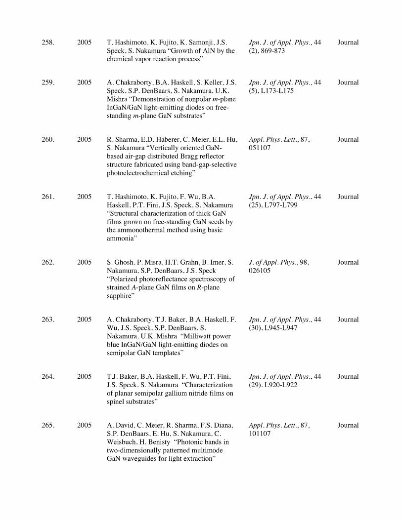
Conference Proceedings
42. 1996 S. Chichibu, T. Azuhata, T. Sota, S. Nakamura “Contribution of excitons in the photoluminescence spectra of h-GaN epitaxial layers grown on sapphire substrates by TF-MOCVD”
International Symposium on Blue Laser and Light Emitting Diodes, March 5-7, pp. 202-205
Conference Proceedings
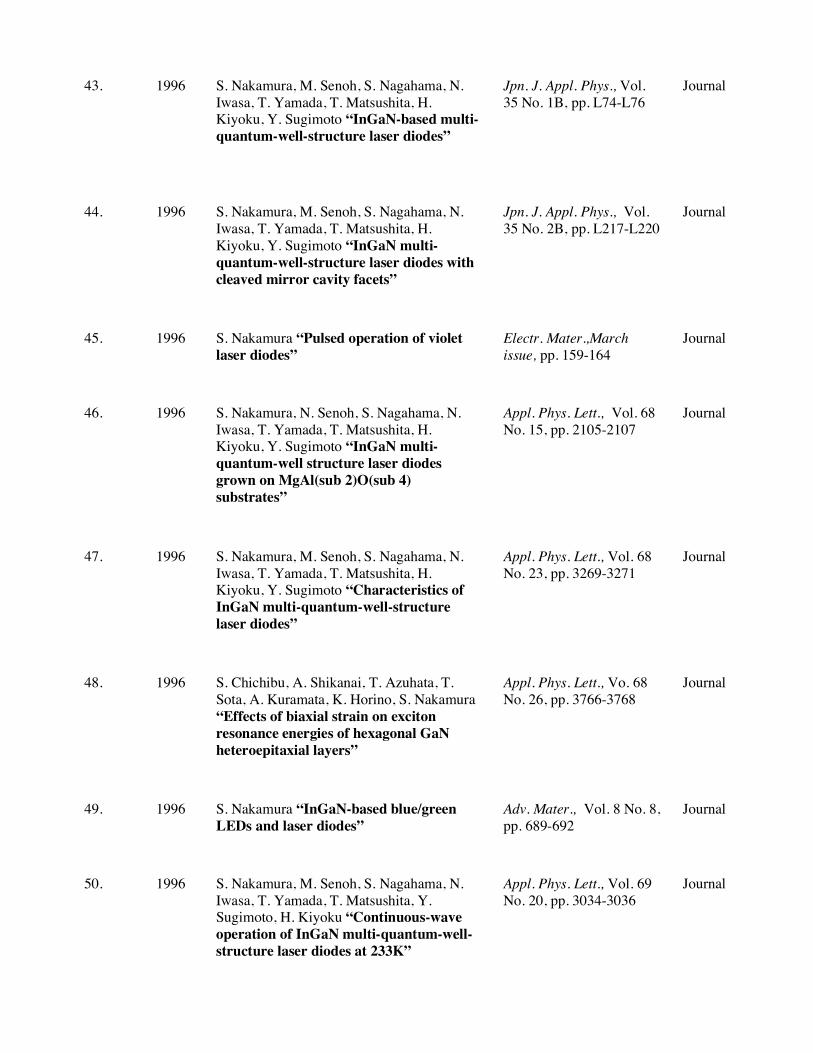
43. 1996 S. Nakamura, M. Senoh, S. Nagahama, N. Iwasa, T. Yamada, T. Matsushita, H. Kiyoku, Y. Sugimoto “InGaN-based multi-quantum-well-structure laser diodes”
Jpn. J. Appl. Phys., Vol. 35 No. 1B, pp. L74-L76
Journal
44. 1996 S. Nakamura, M. Senoh, S. Nagahama, N. Iwasa, T. Yamada, T. Matsushita, H. Kiyoku, Y. Sugimoto “InGaN multi-quantum-well-structure laser diodes with cleaved mirror cavity facets”
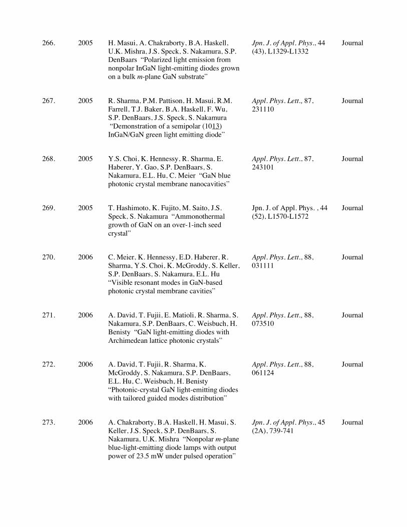
Jpn. J. Appl. Phys., Vol. 35 No. 2B, pp. L217-L220
Journal
45. 1996 S. Nakamura “Pulsed operation of violet laser diodes”
Electr. Mater.,March issue, pp. 159-164
Journal
46. 1996 S. Nakamura, N. Senoh, S. Nagahama, N. Iwasa, T. Yamada, T. Matsushita, H. Kiyoku, Y. Sugimoto “InGaN multi-quantum-well structure laser diodes grown on MgAl(sub 2)O(sub 4) substrates”
Appl. Phys. Lett., Vol. 68 No. 15, pp. 2105-2107
Journal
47. 1996 S. Nakamura, M. Senoh, S. Nagahama, N. Iwasa, T. Yamada, T. Matsushita, H. Kiyoku, Y. Sugimoto “Characteristics of InGaN multi-quantum-well-structure laser diodes”
Appl. Phys. Lett., Vol. 68 No. 23, pp. 3269-3271
Journal
48. 1996 S. Chichibu, A. Shikanai, T. Azuhata, T. Sota, A. Kuramata, K. Horino, S. Nakamura “Effects of biaxial strain on exciton resonance energies of hexagonal GaN heteroepitaxial layers”
Appl. Phys. Lett., Vo. 68 No. 26, pp. 3766-3768
Journal
49. 1996 S. Nakamura “InGaN-based blue/green LEDs and laser diodes”
Adv. Mater., Vol. 8 No. 8, pp. 689-692
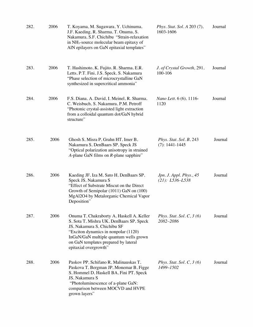
Journal
50. 1996 S. Nakamura, M. Senoh, S. Nagahama, N. Iwasa, T. Yamada, T. Matsushita, Y. Sugimoto, H. Kiyoku “Continuous-wave operation of InGaN multi-quantum-well-structure laser diodes at 233K”
Appl. Phys. Lett., Vol. 69 No. 20, pp. 3034-3036
Journal
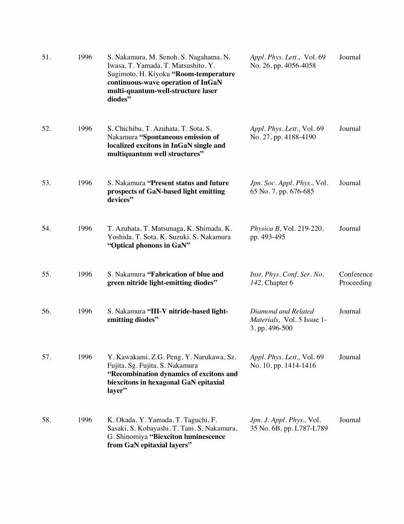
51. 1996 S. Nakamura, M. Senoh, S. Nagahama, N. Iwasa, T. Yamada, T. Matsushito, Y. Sugimoto, H. Kiyoku “Room-temperature continuous-wave operation of InGaN multi-quantum-well-structure laser diodes”
Appl. Phys. Lett., Vol. 69 No. 26, pp. 4056-4058
Journal
52. 1996 S. Chichibu, T. Azuhata, T. Sota, S. Nakamura “Spontaneous emission of localized excitons in InGaN single and multiquantum well structures”
Appl. Phys. Lett., Vol. 69 No. 27, pp. 4188-4190
Journal
53. 1996 S. Nakamura “Present status and future prospects of GaN-based light emitting devices”
Jpn. Soc. Appl. Phys., Vol. 65 No. 7, pp. 676-685
Journal
54. 1996 T. Azuhata, T. Matsunaga, K. Shimada, K. Yoshida, T. Sota, K. Suzuki, S. Nakamura “Optical phonons in GaN”
Physica B, Vol. 219-220, pp. 493-495
Journal
55. 1996 S. Nakamura “Fabrication of blue and green nitride light-emitting diodes”
Inst. Phys. Conf. Ser. No. 142, Chapter 6
Conference Proceeding
56. 1996 S. Nakamura “III-V nitride-based light-emitting diodes”
Diamond and Related Materials, Vol. 5 Issue 1-3, pp. 496-500
Journal
57. 1996 Y. Kawakami, Z.G. Peng, Y. Narukawa, Sz. Fujita, Sg. Fujita, S. Nakamura “Recombination dynamics of excitons and biexcitons in hexagonal GaN epitaxial layer”
Appl. Phys. Lett., Vol. 69 No. 10, pp. 1414-1416
Journal
58. 1996 K. Okada, Y. Yamada, T. Taguchi, F. Sasaki, S. Kobayashi, T. Tani, S. Nakamura, G. Shinomiya “Biexciton luminescence from GaN epitaxial layers”
Jpn. J. Appl. Phys., Vol. 35 No. 6B, pp. L787-L789
Journal
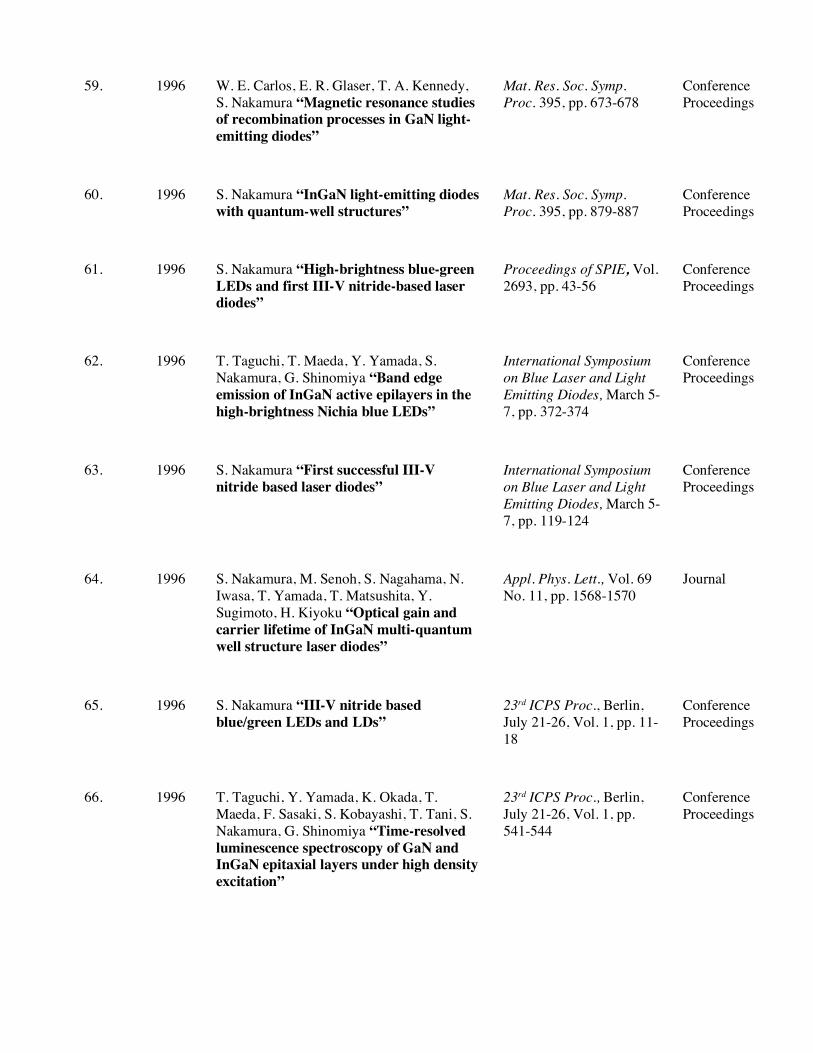
59. 1996 W. E. Carlos, E. R. Glaser, T. A. Kennedy, S. Nakamura “Magnetic resonance studies of recombination processes in GaN light-emitting diodes”
Mat. Res. Soc. Symp. Proc. 395, pp. 673-678
Conference Proceedings
60. 1996 S. Nakamura “InGaN light-emitting diodes with quantum-well structures”
Mat. Res. Soc. Symp. Proc. 395, pp. 879-887
Conference Proceedings
61. 1996 S. Nakamura “High-brightness blue-green LEDs and first III-V nitride-based laser diodes”
Proceedings of SPIE, Vol. 2693, pp. 43-56
Conference Proceedings
62. 1996 T. Taguchi, T. Maeda, Y. Yamada, S. Nakamura, G. Shinomiya “Band edge emission of InGaN active epilayers in the high-brightness Nichia blue LEDs”
International Symposium on Blue Laser and Light Emitting Diodes, March 5-7, pp. 372-374
Conference Proceedings
63. 1996 S. Nakamura “First successful III-V nitride based laser diodes”
International Symposium on Blue Laser and Light Emitting Diodes, March 5-7, pp. 119-124
Conference Proceedings
64. 1996 S. Nakamura, M. Senoh, S. Nagahama, N. Iwasa, T. Yamada, T. Matsushita, Y. Sugimoto, H. Kiyoku “Optical gain and carrier lifetime of InGaN multi-quantum well structure laser diodes”
Appl. Phys. Lett., Vol. 69 No. 11, pp. 1568-1570
Journal
65. 1996 S. Nakamura “III-V nitride based blue/green LEDs and LDs”
23rd ICPS Proc., Berlin, July 21-26, Vol. 1, pp. 11-18
Conference Proceedings
66. 1996 T. Taguchi, Y. Yamada, K. Okada, T. Maeda, F. Sasaki, S. Kobayashi, T. Tani, S. Nakamura, G. Shinomiya “Time-resolved luminescence spectroscopy of GaN and InGaN epitaxial layers under high density excitation”
23rd ICPS Proc., Berlin, July 21-26, Vol. 1, pp. 541-544
Conference Proceedings

67. 1996 W. E. Carlos, E. R. Glaser, T. A. Kennedy, S. Nakamura “Magnetic resonance studies of recombination processes in GaN-based single-quantum-well light-emitting diodes”
23rd ICPS Proc., Berlin, July 21-26, Vol. 4, pp. 2921-2924
Conference Proceedings
68. 1996 S. Nakamura, M. Senoh, S. Nagahama, N. Iwasa, T. Yamada, T. Matsushita, Y. Sugimoto, H. Kiyoku “Ridge-geometry InGaN multi-quantum-well-structure laser diodes”
Appl. Phys. Lett., Vol. 69 No. 10, pp. 1477-1479
Journal
69. 1996 S. Chichibu, T. Azuhata, T. Sota, S. Nakamura “Excitonic emissions from hexagonal GaN epitaxial layers”
J. Appl. Phys., Vol. 79 No. 5, pp. 2784-2786
Journal
70. 1996 K. G. Zolina, V. E. Kudryashov, A. N. Turkin, A. E. Yunovich, S. Nakamura “Luminescence spectra of superbright blue and green InGaN/AlGaN/GaN light-emitting diodes”
MRS Internet Journal of Nitride Semiconductor Research, Vol. 1
Journal
71. 1997 A. Shikanai, T. Azuhata, T. Sota, S. Chichibu, A.Kuramata, K. Horino, S. Nakamura “Biaxial strain dependence of exciton resonance energies in wurzite GaN”
J. Appl. Phys., Vol. 81 No. 1, pp. 417-424
Journal
72. 1997 Y. Narukawa, Y. Kawakami, S. Fujita, S. Fujita, S. Nakamura “Recombination dynamics of localized excitons in In(sub 0.20)Ga(sub 0.80)N-In(sub 0.05)Ga(sub0.95)N multiple quantum wells”
Phys. Rev. B, Vol. 55 No. 4, pp. R1938-R1941
Journal
73. 1997 S. Nakamura, M. Senoh, S. Nagahama, N. Iwasa, T. Yamada, T. Matsushita, Y. Sugimoto, H. Kiyoku “Longitudinal mode spectra and ultrashort pulse generation of InGaN multiquantum well structure”
Appl. Phys. Lett., Vol. 70 No. 5, pp. 616-618
Journal
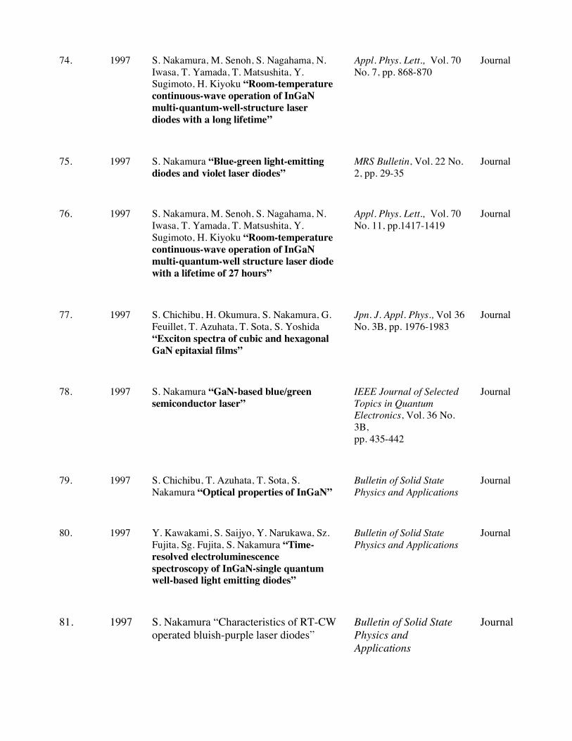
74. 1997 S. Nakamura, M. Senoh, S. Nagahama, N. Iwasa, T. Yamada, T. Matsushita, Y. Sugimoto, H. Kiyoku “Room-temperature continuous-wave operation of InGaN multi-quantum-well-structure laser diodes with a long lifetime”
Appl. Phys. Lett., Vol. 70 No. 7, pp. 868-870
Journal
75. 1997 S. Nakamura “Blue-green light-emitting diodes and violet laser diodes”
MRS Bulletin, Vol. 22 No. 2, pp. 29-35
Journal
76. 1997 S. Nakamura, M. Senoh, S. Nagahama, N. Iwasa, T. Yamada, T. Matsushita, Y. Sugimoto, H. Kiyoku “Room-temperature continuous-wave operation of InGaN multi-quantum-well structure laser diode with a lifetime of 27 hours”
Appl. Phys. Lett., Vol. 70 No. 11, pp.1417-1419
Journal
77. 1997 S. Chichibu, H. Okumura, S. Nakamura, G. Feuillet, T. Azuhata, T. Sota, S. Yoshida “Exciton spectra of cubic and hexagonal GaN epitaxial films”
Jpn. J. Appl. Phys., Vol 36 No. 3B, pp. 1976-1983
Journal
78. 1997 S. Nakamura “GaN-based blue/green semiconductor laser”
IEEE Journal of Selected Topics in Quantum Electronics, Vol. 36 No. 3B, pp. 435-442
Journal
79. 1997 S. Chichibu, T. Azuhata, T. Sota, S. Nakamura “Optical properties of InGaN”
Bulletin of Solid State Physics and Applications
Journal
80. 1997 Y. Kawakami, S. Saijyo, Y. Narukawa, Sz. Fujita, Sg. Fujita, S. Nakamura “Time-resolved electroluminescence spectroscopy of InGaN-single quantum well-based light emitting diodes”
Bulletin of Solid State Physics and Applications
Journal
81. 1997 S. Nakamura “Characteristics of RT-CW operated bluish-purple laser diodes”
Bulletin of Solid State Physics and Applications
Journal
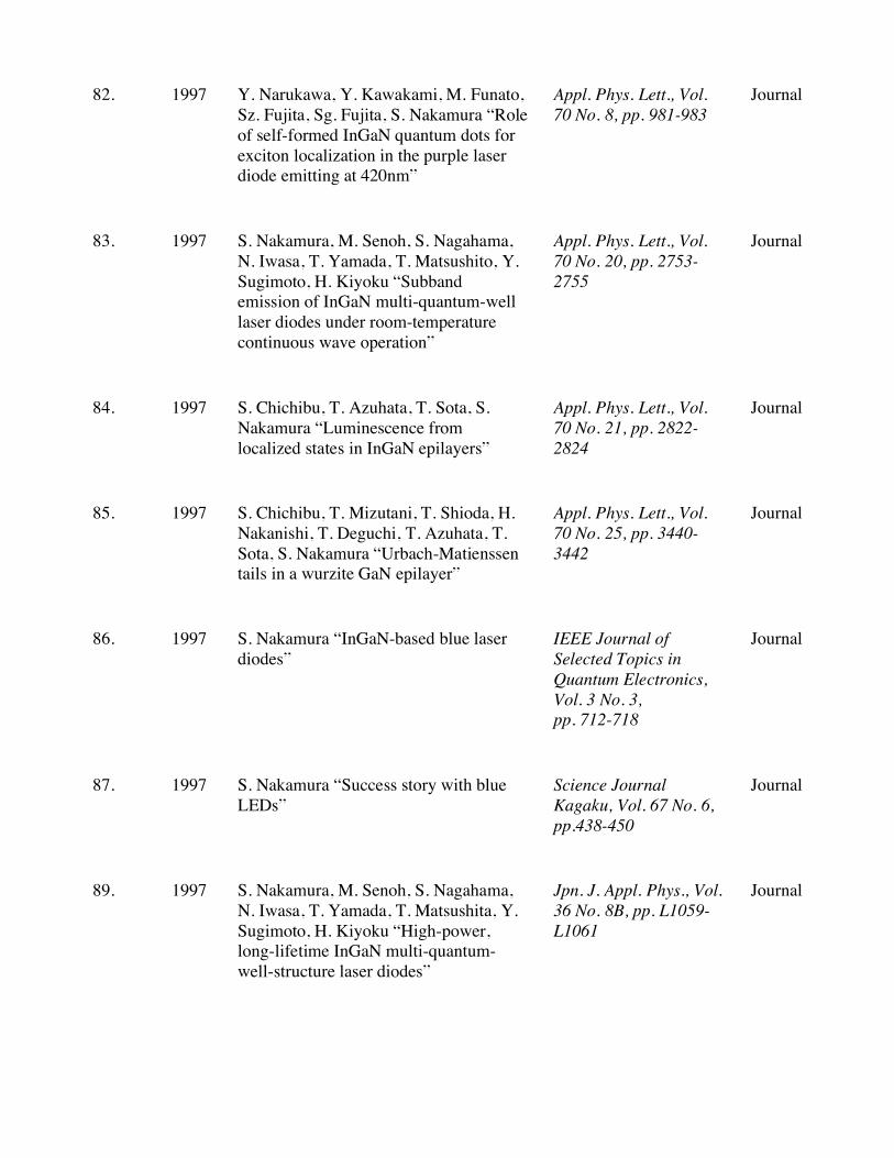
82. 1997 Y. Narukawa, Y. Kawakami, M. Funato, Sz. Fujita, Sg. Fujita, S. Nakamura “Role of self-formed InGaN quantum dots for exciton localization in the purple laser diode emitting at 420nm”
Appl. Phys. Lett., Vol. 70 No. 8, pp. 981-983
Journal
83. 1997 S. Nakamura, M. Senoh, S. Nagahama, N. Iwasa, T. Yamada, T. Matsushito, Y. Sugimoto, H. Kiyoku “Subband emission of InGaN multi-quantum-well laser diodes under room-temperature continuous wave operation”
Appl. Phys. Lett., Vol. 70 No. 20, pp. 2753-2755
Journal
84. 1997 S. Chichibu, T. Azuhata, T. Sota, S. Nakamura “Luminescence from localized states in InGaN epilayers”
Appl. Phys. Lett., Vol. 70 No. 21, pp. 2822-2824
Journal
85. 1997 S. Chichibu, T. Mizutani, T. Shioda, H. Nakanishi, T. Deguchi, T. Azuhata, T. Sota, S. Nakamura “Urbach-Matienssen tails in a wurzite GaN epilayer”
Appl. Phys. Lett., Vol. 70 No. 25, pp. 3440-3442
Journal
86. 1997 S. Nakamura “InGaN-based blue laser diodes”
IEEE Journal of Selected Topics in Quantum Electronics, Vol. 3 No. 3, pp. 712-718
Journal
87. 1997 S. Nakamura “Success story with blue LEDs”
Science Journal Kagaku, Vol. 67 No. 6, pp.438-450
Journal
89. 1997 S. Nakamura, M. Senoh, S. Nagahama, N. Iwasa, T. Yamada, T. Matsushita, Y. Sugimoto, H. Kiyoku “High-power, long-lifetime InGaN multi-quantum-well-structure laser diodes”
Jpn. J. Appl. Phys., Vol. 36 No. 8B, pp. L1059-L1061
Journal

90. 1997 S. Chichibu, K. Wada, S. Nakamura “Spatially resolved cathodoluminescence spectra of InGaN quantum wells”
Appl. Phys. Lett., Vol. 71 No. 16, pp. 2346-2348
Journal
91. 1997 S. Nakamura, M. Senoh, S. Nagahama, N. Iwasa, T. Yamada, T. Matsushita, H. Kiyoku, Y. Sugimoto, T. Kozaki, H. Umemoto, M. Sano, K. Chocho “InGaN/GaN/AlGaN-based laser diodes with modulation-doped strained-layer superlattices”
Jpn. J. Appl. Phys., Vol. 36 No. 12A, pp. L1568-L1571
Journal
92. 1997 S. Nakamura “InGaN quantum-well structure blue LEDs and LDs”
Journal of Luminescence, Vol. 72-74, pp. 55-58
Journal
93. 1997 S. Nakamura “Present and future aspects of blue light emitting devices”
Applied Surface Science, Vol. 113-114, pp. 689-697
Journal
94. 1997 S. Nakamura “First III-V-nitride-based violet laser diodes”
J. Cryst. Growth, Vol. 170 Issue 1-4, pp. 11-15
Journal
95. 1997 S. Nakamura “First laser-diodes fabricated from III-V nitride based materials”
Mater. Sci. & Engin. B, Vol. 43 Issue 1-3, pp. 258-264
Journal
96. 1997 S. Nakamura “III-V nitride based light-emitting devices”
Solid State Communications, Vol. 102 No. 2-3, pp. 237-248
Journal
97. 1997 S. Nakamura “RT-CW operation of InGaN multi-quantum-well structure laser diodes”
Mater. Sci. & Engin. B, Vol. 50 Issue 1-3, pp. 277-284
Journal

98. 1997 S. Nakamura “Group III-V nitride-based ultraviolet blue-green-yellow light-emitting diodes and laser diodes”
Semiconductors & Semimetals, Vol. 48, pp. 391-443
Journal
99. 1997 G. Mohs, T. Aoki, M. Nagai, R. Shimano, M. Kuwata-Gonokami, S. Nakamura “Failure of the modal gain model in a GaN based laser diode”
Solid State Communications, Vol. 104 No. 11, pp. 643-648
Journal
100. 1997 S. Nakamura “Lessons from research of blue LEDs”
J. Phys. Soc. Jpn., Vol. 52 No. 12, pp.924-925
Journal
101. 1997 S. Nakamura “Room-temperature CW operation of GaN based laser diodes”
The Review of Laser Engineering, Vol. 25 No. 7, pp. 498-503
Journal
102. 1997 S. Nakamura “How I was led to the discovery of the InGaN-based blue/green LEDs”
Semiconductor News, July-December 1997, pp. 87-92
Magazine
103. 1997 F. A. Ponce, D. Cherns, W. T. Young, J. W. Steeds, S. Nakamura “Observation of nanopipes and inversion domains in high quality GaN epitaxial layers”
Mat. Res. Soc. Proc., 449, pp. 405-410
Conference Proceedings
104. 1997 S. Chichibu, T. Azuhata, T. Sota, S. Nakamura “Recombination of localized excitons in InGaN single and multi-quantum well structures”
Mat. Res. Soc. Proc., 449, pp. 653-658
Conference Proceedings
105. 1997 Y. Narukawa, Y. Kawakami, Sz. Fujita, Sg. Fujita, S. Nakamura “Emission mechanism of the InGaN MQW grown by MOCVD”
Mat. Res. Soc. Proc., 449, pp. 665-670
Conference Proceedings
106. 1997 W. E. Carlos, E. R. Glaser, T. A. Kennedy, S. Nakamura “Magnetic resonance studies of GaN-based single quantum well LEDs”
Mat. Res. Soc. Symp. Proc., 449, pp. 757-767
Conference Proceedings
107. 1997 S. Nakamura “Characteristics of InGaN multi-quantum-well structure laser diodes”
Mat. Res. Soc. Symp. Proc., 449, pp. 1135-1142
Conference Proceedings
108. 1997 S. Nakamura “Characteristics of RT-CW operated InGaN multi-quantum-well-structure laser diodes”
MRS Internet J. Nitride Semicond. Res. 2, 5
Journal
109. 1997 M. Yamaguchi, T. Yagi, T. Azuhata, T. Sota, K. Suzuki, S. Chichibu, S. Nakamura “Brillouin scattering study of gallium nitride: elastic stiffness constants”
Journal of Physics: Condensed Matter, Vol. 9 No. 1, pp. 241-248
Journal
110. 1997 S. Nakamura “Present performance of InGaN based blue/green/yellow LEDs”
Proceedings of SPIE, Vol. 3002, pp. 26-35
Conference Proceedings
111. 1997 T. Deguchi, A. Shikanai, T. Sota, S. Chichibu, N. Sarukura, H. Ohtaka, T. Yamanaka, S. Nakamura “Nanosecond pump-and-probe study of wurtzite GaN”
Materials Science and Engineering, B50, pp. 180-182
Journal
112. 1997 T. Deguchi, T. Azuhata, T. Sota, S. Chichibu, S. Nakamura “Gain spectra in cw InGaN/GaN MQW laser diodes”
Materials Science and Engineering, B50, pp. 251-255
Journal
113. 1997 Y. Kawakami, Y. Narukawa, K. Sawada, S. Saijo, Sz. Fujita, Sg. Fujita, S. Nakamura “Recombination dynamics of localized excitons in self-formed InGaN quantum dots”
Materials Science and Engineering B, Vol. 50 Issue 1-3, pp. 256-263
Journal
114. 1997 V. E. Kudryashov, A. N. Turkin, A. E. Yunovich, K. G. Zolina, S. Nakamura “Spectra of superbright blue and green InGaN/AlGaN/GaN light-emitting diodes”
J. Eur. Ceram. Soc., Vol. 17 No. 15/16, pp. 2033-2037
Journal
115. 1997 D. Cherns, W. T. Young, M. A. Saunders, F. A. Ponce, S. Nakamura “The analysis of nanopipes and inversion domains in GaN thin films”
Inst. Phys. Conf. Ser., No. 157, pp. 187-190
Conference Proceedings
116. 1997 S. Nakamura “Present status and future of blue LEDs and LDs”
Rev. Laser Engin., Vol. 25 No. 12, pp. 850-854
Journal
117. 1997 D. Cherns, W. T. Young, J. W. Steeds, F. A. Ponce, S. Nakamura “Observation of coreless dislocations in alpha-GaN”
Journal Crystal Growth, Vol. 178 No. 1-2, pp. 201-206
Journal
118. S. Nakamura, G. Fasol The Blue Laser Diode (The Complete Story)
Springer-Verlag: Heidelberg
Book
119. 1998 S. Nakamura, M. Senoh, S. Nagahama, N. Iwasa, T. Yamado, T. Matsushita, H. Kiyoku, V. Sugimoto, T. Kozaki, H. Umemoto, M. Sano, K. Chocho “InGaN/GaN/AlGaN-based laser diodes with modulation-doped strained-layer superlattices grown on an epitaxially laterally overgrown GaN substrate”
Appl. Phys. Lett., Vol. 72 No. 2, pp. 211-213
Journal
120. 1998 S. Nakamura “Applications of LEDs and LDs”
Semiconductors & Semimetals, Vol. 50, pp. 431-457
Journal
121. 1998 S. Nakamura “Progress with GaN-based blue/green LEDs and bluish-purple semiconductor LDs”
Electronics and Communications in Japan, Vol. 81 No. 5, pp. 1-8
Journal

122. 1998 A. Alemu, B. Gil, M. Julier, S. Nakamura “Optical properties of wurzite GaN epilayers growns on A-plane sapphire”
Phys. Rev. B, Vol. 57 No.7, pp. 3761-3764
Journal
123. 1998 S. Nakamura “Light emission moves into blue”
Physics World, February 1998
Magazine
124. 1998 M. Julier, J. Campo, B. Gil, J.P. Lascaray, S. Nakamura “Determination of the spin-exchange interaction constant in wurzite GaN”
Phys. Rev. B, Vol. 57 No. 12, pp. R6791-R6794
Journal
125. 1998 S. Nakamura, M. Senoh, S. Nagahama, N. Iwasa, T. Yamada, T. Matsushita, H. Kiyoku, Y. Sugimoto, T. Kozaki, H. Umemoto, M. Sano, K. Chocho “High-power, long-lifetime InGaN/GaN/AlGaN-based laser diodes grown on pure GaN substrates”
Jpn. J. Appl. Phys., Vol. 37 No. 3B, pp. L309-L312
Journal
126. 1998 S. Nakamura, M. Senoh, S. Nagahama, N. Iwasa, T. Yamada, T. Matsushita, H. Kiyoku, Y. Sugimoto, T. Kazaki, H. Umemoto, M. Sano, K. Chocho “Continuous-wave operation of InGaN/GaN/AlGaN-based laser diodes grown on GaN substrates”
Appl. Phys. Lett., Vol. 72 No. 16, pp. 2014-2016
Journal
127. 1998 S. Nakamura “InGaN multiquantum-well-structure laser diodes with GaN-AlGaN modulation-doped strained layer superlattices”
IEEE Journal of Selected Topics in Quantum Electronics, Vol. 4 No. 3, pp. 483-489
Journal
128. 1998 S. Nakamura, M. Senoh, S. Nagahama, N. Iwasa, T. Yamada, T. Matsushita, H. Kiyoku, Y. Sugimoto, T. Kozaki, H. Umemoto, M. Sano, K. Chocho “Violet InGaN/GaN/AlGaN-based laser diodes with an output power of 420mW”
Jpn. J. Appl. Phys., Vol. 37 No. 6A, pp. L627-L629
Journal

129. 1998 T. Mukai, K. Takekawa, S. Nakamura “InGaN-based blue light-emitting diodes grown on epitaxially laterally overgrown GaN substrates”
Jpn. J. Appl. Phys., Vol. 37 No. 7B, pp. L839-L841
Journal
130. 1998 S. Chichibu, T. Sota, K. Wada, S. Nakamura “Exciton localization in InGaN quantum well devices”
J. Vac. Sci. Technol. B, Vol. 16 No. 4, pp. 2204-2214
Journal
131. 1998 S. Nakamura, M. Senoh, S. Nagahama, N. Iwasa, T. Yamada, T. Matsushita, H. Kiyoku, Y. Sugimoto, T. Kozaki, H. Umemoto, M. Sano, K. Chocho “InGaN/GaN/AlGaN-based laser diodes with cleaved facets grown on GaN substrates”
Appl. Phys. Lett., Vol. 73 No. 6, pp. 832-834
Journal
132. 1998 S. Nakamura “The roles of structural imperfections in InGaN-based blue light-emitting diodes and laser diodes”
Science, Vol. 281 No. 5379, pp. 956-961
Journal
133. 1998 T. Mukai, M. Yamada, S. Nakamura “Current and temperature dependences of electroluminescence of InGaN-based UV/blue/green light-emitting diodes”
Jpn. J. Appl. Phys., Vol. 37, pp. L1358-L1361
Journal
134. 1998 S. Nakamura “Materials issues for InGaN-based lasers”
J. Elect. Mater., Vol. 27 No. 4, pp. 160-165
Journal
135. 1998 S. Nakamura “Cathodoluminescence study on quantum microstructures”
Jpn. Soc. Appl. Phys., Vol. 67 No. 7, pp. 798-801
Journal
136. 1998 T. Mukai, D. Morita, S. Nakamura “High-power UV InGaN/AlGaN double-heterostructure LEDs”
J. Cryst. Growth, Vol. 189/190, pp. 778-781
Journal
137. 1998 G. Mohs, T. Aoki, R. Shimano, M. Kuwata-Gonokami, S. Nakamura “On the grain mechanism in GaN based laser diodes”
Solid State Communications, Vol. 108 No. 2, pp. 105-110
Journal
138. 1998 S. Nakamura “InGaN-based laser diodes”
Annu. Rev. Mater. Sci., Vol. 28, pp. 125-152
Journal
139. 1998 A. Alemu, M. Julier, J. Campo, B. Gil, D. Scalbert, J.-P. Lascaray “Optical anisotropy in GaN grown onto A-plane sapphire”
E-MRS ’98 Spring Meeting, Strasbourg, France
Conference proceeding
140. 1998 T. Deguchi, A. Shikanai, K. Torii, T. Sota, S. Chichibu, S. Nakamura “Luminescence spectra from InGaN multiquantum wells heavily doped with Si”
Appl. Phys. Lett., Vol. 72 No. 25, pp. 3329-3331
Journal
141. 1998 K. Ando, T. Yamaguchi, K. Koizumi, Y. Okuno, T. Abe, H. Kasada, A. Ishibashi, K. Nakano, S. Nakamura “Deep defect center characteristics of wide-bandgap II-IV and III-V blue laser materials”
Proceedings of SPIE (1998, Jan. 26-29), San Jose, California
Conference proceeding
142. 1998 S. Nakamura “InGaN/GaN/AlGaN-based laser diodes with an estimated lifetime of longer than 10,000 hours”
MRS Bulletin, Vol. 23 No. 5, pp. 37-43
Journal
143. 1998 S. Nakamura, K. Kitamura, H. Umeya, H. Jia, M. Kobayashi, A. Yoshikawa, M. Shimotomai, Y. Kato, K. Takahashi “Bright electroluminescence from CdS quantum dot LED structures”
Electronics Letters, Vol. 34 No. 25, pp. 2435-2436
Journal
144. 1998 E.R. Glaser, T.A. Kennedy, W.E. Carlos, P.P. Ruden, S. Nakamura “Recombination processes in In/sub x/Ga/sub 1-x/N light-emitting diodes studied through optically detected magnetic resonance”
Appl. Phys. Lett., Vol. 73 No. 21, pp. 3123-3125
Journal
145. 1998 S. Nakamura, Y. Ueno, K. Tajima “Ultrafast (200-fs switching, 1.5-Tb/s demultiplexing) and high-repetition (10 GHz) operations of a polarization-discriminating symmetric Mach-Zehnder all-optical switch”
IEEE Photonics Technology Letters, Vol. 10 No. 11, pp. 1572-1574
Journal
146.
1998 Y. Kamiura, Y. Yamashita, S. Nakamura “Photo-enhanced activation of hydrogen-passivated magnesium in p-type GaN films”
Jpn. J. Appl. Phys., Vol. 37 No. 8B, pp. L970-L971
Journal
147.
1998 Y. Kawakami, Y. Narukawa, K. Sawada, S. Nakamura “The mechanism of radiative recombination in light-emitting devices composed on InGaN quantum wells”
Electronics and Communications in Japan, Vol. 81 No. 7, pp. 45-56
Journal
148. 1998 K. Wada, S. Chichibu, S. Nakamura, T. Sota, A. Kozen, T. Murashita “Cathodoluminescence study of quantum microstructures”
Oyo Buturi, Vol. 67 No. 7, pp. 789-801
Journal
149. 1998 S. Nakamura “Commercial blue LDs a step closer for Nichia”
III-Vs Review, Vol. 11 No.2, pp. 28-32
Journal
150. 1998 T. Deguchi, T. Azuhata, T. Sota, S. Chichibu, M. Arita, H. Nakanishi, S. Nakamura “Gain spectroscopy of continuous wave InGaN multi-quantum well laser diodes”
Semicond. Sci. and Technol., Vol. 13 No. 1, pp. 97-101
Journal

151. 1998 Y. Kawakami, Y. Narukawa, K. Sawada, S. Saijyo, S. Fujita, S. Fujita, S. Nakamura “The mechanism of radiative recombination in light emitting devices composed of InGaN quantum wells”
Transactions of the Institute of Electronics, Information and Communication Engineers C-II, Vol. J81C-II No. 1, pp. 78-88
Journal
152. 1998 T. Mukai, H. Narimatsu, S. Nakamura “Amber InGaN-based light-emitting diodes operable at high ambient temperatures”
Jpn. J. Appl. Phys., Vol. 37 No. 5A, pp. L479-L481
Journal
153. 1998 Z. L. Weber, S. Ruvimov, W. Swider, Y. Kim, J. Washburn, S. Nakamura, R. S. Kern, Y. Chen, J. W. Yang “Role of dopants and impurities on pinhole formation; defects formed at InGaN/GaN and AlGaN/GaN quantum wells”
Mat. Res. Soc. Symp. Proc., Vol. 482, pp. 375-380
Journal
154. 1998 S. Chichibu, T. Deguchi, T. Sota, K. Wada, S. Nakamura “Localized excitons in InGaN”
Mat. Res. Soc. Symp. Proc., Vol. 482, pp. 613-624
Conference Proceedings
155. 1998 S. Nakamura “InGaN/GaN/AlGaN-based laser diodes with an estimated lifetime of longer than 10,000 hours”
Mat. Res. Soc. Symp. Proc., Vol. 482, pp. 1145-1156
Conference Proceedings
156. 1998 Y. Narukawa, S. Saijyo, Y. Kawakami, Sz. Fujita, Sg. Fujita, S. Nakamura “Time-resolved electroluminescence spectroscopy of InGaN single quantum well LEDs”
J. Crystal Growth, Vol. 189/190, pp. 593-596
Journal
157. 1998 Y. Narukawa, K. Sawada, Y. Kawakami, Sz. Fujita, Sg. Fujita, S. Nakamura “Emission mechanism of localized excitons in InGaN single quantum wells”
J. Crystal Growth, Vol. 189/190, pp. 606-610
Journal
158. 1998 W. E. Carlos, S. Nakamura “Magnetic resonance studies of GaN-based LEDs”
J. Crystal Growth, Vol. 189/190, pp. 794-797
Journal
159. 1998 Y. Zohta, H. Kuroda, R. Nii, S. Nakamura “Frequency dependence of the reverse-biased capacitance of blue and green light-emitting diodes”
J. Crystal Growth, Vol. 189/190, pp. 816-819
Journal
160. 1998 S. Nakamura, M. Senoh, S. Nagahama, N. Iwasa, T. Yamada, T. Matsushita, H. Kiyoku, Y. Sugimoto, T. Kozaki, H. Umemoto, M. Sano, K. Chocho “Present status of InGaN/GaN/AlGaN-based laser diodes”
J. Crystal Growth, Vol. 189/190, pp. 820-825
Journal
161. 1998 S. Nakamura “High-power InGaN-based blue laser diodes with a long lifetime”
J. Crystal Growth, Vol. 195, pp. 242-247
Journal
162. 1998 S. Chichibu, H. Marchand, M. S. Minsky, S. Keller, P. T. Fini, J. P. Ibbetson, S. B. Fleischer, J. S. Speck, J. E. Bowers, E. Hu, U. K. Mishra, S. P. DenBaars, T. Deguchi, T. Sota, S. Nakamura “Emission mechanisms of bulk GaN and InGaN quantum wells prepared by lateral epitaxial overgrowth”
Appl. Phys. Lett., Vol. 74 No. 10, pp. 1460-1462
Journal
163. 1998 S. Nakamura “Recent developments in InGaN-based LEDs and LDs”
Acta Physica Polonica A, Vol. 95, pp. 153-164
Journal
164. 1998 S. Nakamura, M. Senoh, S.-I. Nagahama, N. Iwasa, T. Yamada, T. Matsushita, H. Kiyoku, Y. Sugimoto, T. Kozaki, I. Umemoto, M. Sano, K. Chocho “InGaN/GaN/AlGaN-based laser diodes grown on GaN substrates with a fundamental transverse mode”
Jpn. J. Appl. Phys., Vol. 37 Part 2 No. 9A-B, L1020-L1022
Journal

165. 1998 S. Nakamura “Progress of GaN-based blue/green LEDs and bluish-purple semiconductor LDs”
Trans. Inst. Electron. Inf. Comm. Engin., Vol. J81C-II No. 1, pp. 89-96
Journal
166. 1998 D. Cherns, W. T. Young, M. Sanders, J. W. Steeds, F. A. Ponce, S. Nakamura “Determination of the atomic structure of inversion domain boundaries in alpha-GaN by transmission electron microscopy”
Philosophical Magazine A (Physics of Condensed Matter: Structure, Defects, and Mechanical Properties), Vol. 77 No. 1, pp. 273-286
Magazine
167. 1999 T. Mukai, M. Yamada, S. Nakamura “InGaN-based UV/blue/green/amber/red LEDs”
Light Emitting Diodes: Research, Manufacturing, and Applications III (SPIE), Vol. 3621
Journal
168. 1999 T. Azuhata, K. Shimada, T. Deguchi, T. Sota, K. Suzuki, S. Chichibu, S. Nakamura “Infrared lattice absorption in wurtzite GaN”
Jpn. J. Appl. Phys., Vol. 38 No. 2B, pp. L151-L153
Journal
169. 1999 S. Nakamura, M. Senoh, S. Nagahama, T. Matsushita, H. Kiyoku, Y. Sugimoto, T. Kozaki, H. Umemoto, M. Sano, T. Mukai “Violet InGaN/GaN/AlGaN-based laser diodes operable at 50˚ C with a fundamental transverse mode”
Jpn. J. Appl. Phys., Vol. 38 No. 3A, pp. L226-L229
Journal
170. 1999 S.F. Chichibu, H. Marchand, M.S. Minskey, S. Keller, P.T. Fini, J.P. Ibbetson, S.B. Feisher, J.S. Speck, J.E. Bowers, E. Hu, U.K. Mishra, S.P. DenBaars, T. Deguchi, T. Sota, S. Nakamura “Emission mechanisms of bulk GaN and InGaN quantum wells prepared by lateral epitaxial overgrowth”
Appl. Phys. Lett., Vol. 74 No. 10, pp. 1460-1462
Journal
171. 1999 M. Yamaguchi, T. Yagi, T. Sota, T. Deguchi, K. Shimada, S. Nakamura “Brillouin scattering study of bulk GaN”
J. Appl. Phys., Vol. 85 No. 12, pp. 8502-8504
Journal

172. 1999 S. Nakamura “InGaN/GaN/AlGaN-based laser diodes grown on epitaxially laterally overgrown GaN’
J. Mater. Rsrch., Vol. 14 No. 7, pp. 2716-2731
Journal
173. 1999 K. Torii, T. Deguchi, T. Sota, K. Suzuki, S. Chichibu, S. Nakamura “Reflectance and emission spectra of excitonic polaritons in GaN”
Phys. Rev. B, Vol. 60 No. 7, pp. 4723-4730
Journal
174. 1999 T. Deguchi, K. Torii, K. Shimada, T. Sota, R. Matsuo, M. Sugiyami, A. Setoguchi, S. Chichibu, S. Nakamura “Optical properties of InGaN active layer in ultraviolet light-emitting diode”
Jpn. J. Appl. Phys., Vol. 38 No. 9A/B, pp. L975-L977
Journal
175. 1999 J.T. Torvik, J.I. Pankove, S. Nakamura, I. Grzegory, S. Porowski “The effect of threading dislocations, Mg-doping, and etching on the spectral responsivity in GaN-based ultraviolet detectors”
J. Appl. Phys., Vol. 86 No. 8, pp. 4588-4593
Journal
176. 1999 T. Mukai, S. Nakamura “Ultraviolet InGaN and GaN single-quantum-well-structure light-emitting diodes grown epitaxially laterally overgrown GaN substrates”
Jpn. J. Appl. Phys., Vol. 38 No. 10, pp. 5735-5739
Journal
177. 1999 S. Nakamura “InGaN-based blue light-emitting diodes and laser diodes”
J. Cryst. Growth, Vol. 201/202, pp. 290-295
Journal
178. 1999 S. Nakamura “Present status of InGaN-based laser diodes”
Phys. Stat. Sol. (a), Vol. 176 Issue 1, pp. 15-22
Journal
179. 1999 S. Nakamura “InGaN/GaN/AlGaN-based laser diodes grown on free-standing GaN substrates”
Mater. Sci. & Engin. B, Vol. 59 Issue 1-3, pp. 370-375
Journal
180. 1999 Y. Kamiura, Y. Yamashita, S. Nakamura “Photo-enhanced dissociation of hydrogen-magnesium complexes in gallium nitride”
Physica B, Vol. 273/274, pp. 54-57
Journal
181. 1999 H. Asahi, K. Iwata, H. Tampo, T. Kuroiwa, M. Hiroki, K. Asami, S. Nakamura, S. Gonda “Very strong photoluminescence emission from GaN grown on amorphous silica, substrate by gas source MBE”
J. Cryst. Growth, Vol. 201/202, pp. 371-375
Journal
182. 1999 S. Nakamura “Blue light emitting laser diodes”
Thin Solid Films, Vol. 343-344, pp. 345-349
Journal
183. 1999 S.F. Chichibu, A.C. Abare, M.P. Mack, M.S. Minsky, T. Deguchi, D. Cohen, P. Kozodoy, S.B. Fleisher, S. Keller, J.S. Speck, J.E. Bowers, E. Hu, U.K. Mishra, L.A. Coldren, S.P. DenBaars, K. Wada, T. Sota, S. Nakamura “Optical properties of InGaN quantum wells”
Mater. Sci. & Engin. B, Vol. 59 Issue 1-3, pp. 298-306
Journal
184. 1999 S. Nakamura “InGaN-based violet laser diodes”
Semicond, Sci. Technol., Vol. 14 No. 6, pp. R27-R40
Journal
185. 1999 S. Nakamura “Development of violet InGaN-based laser diodes”
Jpn. Soc. Appl. Phys., Vol. 68 No. 7, pp. 793-796
Journal
186. 1999 T. Deguchi, D. Ichiryu, K. Toshikawa, K. Sekiguchi, T. Sota, R. Matsuo, T. Azuhata, M. Yamaguchi, T. Yagi, S. Chichibu, S. Nakamura “Structural and vibrational properties of GaN”
J. Appl. Phys., Vol. 86 No. 4, pp. 1860-1866
Journal
187. 1999 T.J. Ochalski, B. Gil, P. Lefebvre, N. Grandjean, M. Leroux, J. Massies, S. Nakamura, H. Morkoc “Photoreflectance investigations of the bowing parameter in AlGaN alloys lattice-matched to GaN”
Appl. Phys. Lett., Vol. 74 No. 22, pp. 3353-3355
Journal
188. 1999 Y. Narukawa, Y. Kawakami, Sg. Fujita, S. Nakamura “Dimensionality of excitons in laser-diode structures composed of In(sub x)Ga(sub 1-x)N multiple quantum wells”
Phys. Rev. B, Vol. 59 No. 15, pp. 10283-10288
Journal
189. 1999 S. Nakamura “Development of violet InGaN-based laser diodes”
Oyo Buturi, Vol. 68 No. 7, pp. 793-796
Journal
190. 1999 T. Azuhata, K. Shimada, T. Deguchi, T. Sota, R. Matsuo, M. Sugiyama, A. Setoguchi, S. Chichibu, S. Nakamura “Optical properties of an InGaN active layer in ultraviolet light emitting diode”
Jpn. J. Appl. Phys., Vol. 38 No. 9 A/B, pp. L975-L977
Journal
191. 1999 T. Deguchi, K. Sekiguchi, A. Nakamura, T. Sota, R. Matsuo, S. Chichibu, S. Nakamura “Quantum-confined Stark effect in an AlGaN/GaN/AlGaN single quantum well structure”
Jpn. J. Appl. Phys., Vol. 38 No. 8B, pp. L914-L916
Journal
192. 1999 T. Mukai, M. Yamada, S. Nakamura “Characteristic of InGaN-based UV/blue/green/amber/red light emitting diode”
Jpn. J. Appl. Phys., Vol. 38 No. 7A, pp. 3976-3981
Journal
193. 1999 T. Mukai, S. Nakamura “White and UV LEDs”
Oyo Buturi, Vol. 68 No. 2, pp. 152-155
Journal
194. 1999 Y. Narukawa, S. Saijou, Y. Kawakami, S. Fujita, T. Mukai, S. Nakamura “Radiative and nonradiative recombination processes in ultraviolet light-emitting diode composed of an In/sub0.02/Ga/sub 0.98/N active layer”
Appl. Phys. Lett., Vol. 74 No. 4, pp. 558-560
Journal
195. 1999 S.F. Chichibu, K. Sota, K. Wada, S.P. DenBaars, S. Nakamura “Spectroscopic studies in InGaN quantum wells”
MRS Internet Journal of Nitride Semiconductor Research, Vol. 4s1, 2.7
Journal
196. 1999 S. Nakamura, M. Senoh, S. Nagahama, N. Iwasa, T. Matsushita, T. Mukai “InGaN/GaN/AlGaN-based LEDs and laser diodes”
MRS Internet Journal of Nitride Semiconductor Research, Vol. 4s1, 1.1
Journal
197. 1999 S.F. Chichibu, T. Deguchi, T. Sota, K. Wada, S.P. DenBaars, T. Mukai, S. Nakamura “Properties of quantum well excitons in GaN/AlGaN and InGaN/GaN/AlGaN UV, blue, green, amber light emitting diode structures”
Phys. Stat. Sol., Vol. 176 Issue 1, pp. 85-90
Journal
198. 1999 T. Azuhata, K. Shimada, T. Deguchi, T. Sota, K. Suzuki, S. Chichibu, S. Nakamura “Two-phonon absorption spectra in wurzite GaN”
Applied Physics Letters, Vol. 75 No. 14, pp. 2076-2078
Journal
199. 1999 T. A. Kennedy, E. R. Glaser, W. E. Carlos, P. P. Ruden, S. Nakamura “Symmetry of electrons and holes in lightly photo-excited InGaN LEDs”
MRS Internet Journal of Nitride Semiconductor Research, Vol. 4S1, G7.4
Journal
200. 2000 S. Nakamura, F. Chichibu Introduction to Nitride Semiconductor Blue Lasers and Light Emitting Diodes
Taylor & Francis: London and New York
Book
201. 2000 S. Nakamura, S. Pearton, G. Fasol The Blue Laser Diode (The Complete Story) 2nd Ed.
Springer-Verlag: Heidelberg
Book
202. 2000 S. Nakamura “InGaN-based laser diodes” Japan Society of Applied Physics International, No. 1
Journal
203. 2000 S.F. Chichibu, K. Torii, T. Deguchi, T. Sota, A. Setoguchi., H. Nakanishi, T. Azuhata, S. Nakamura “Photoreflectance spectra of excitonic polaritons in GaN substrate prepared by lateral epitaxial overgrowth”
Appl. Phys. Lett., Vol. 76 No. 12, pp. 1576-1578
Journal
204. 2000 S.F. Chichibu, K. Wada, J. Mullhauser, O. Brandt, K.H. Ploog, T. Mizutani, A. Setoguchi, R. Nakai, M. Sugiyama, H. Nakanishi, K. Torii, T. Deguchi, T. Sota, S. Nakamura “Evidence of localization effects in InGaN single-quantum-well ultraviolet light-emitting diodes”
Appl. Phys. Lett., Vol. 76 No. 13, pp. 1671-1673
Journal
205. 2000 S.F. Chichibu, A. Shikanai, T. Deguchi, A. Setoguchi, R. Nakai, H. Nakanishi, K. Wada, S.P. DenBaars, T. Sota, S. Nakamura “Comparison of optical properties of GaN/AlGaN and InGaN/AlGaN single quantum wells”
Jpn. J. Appl. Phys., Vol. 39 No. 4B, pp. 2417-2424
Journal
206. 2000 S. Nakamura “Role of alloy fluctuations in InGaN-based LEDs and laser diodes”
Mater. Sci. Forum, Vols. 338-342, pp. 1609-1614
Journal
207. 2000 S.F. Chichibu, A. Setoguchi, T. Azuhata, J. Mullhauser, M. Sugiyama, T. Mizutani, T. Deguchi, H. Nakanishi, T. Sota, O. Brandt, K.H. Ploog, T. Mukai, S. Nakamura “Effective localization of quantum well excitons in InGaN quantum well structures with high InN mole fraction”
Phys. Stat. Sol. (a), Vol. 180, pp. 321-325
Journal
208. 2000 S.F. Chichibu, T. Azuhata, T. Sota, T. Mukai, S. Nakamura “Localized quantum well excitons in InGaN single-quantum-well amber light-emitting diodes”
J. Appl. Phys., Vol. 88 No. 9, pp. 5153-5157
Journal
209. 2000 S. Nakamura “InGaN-based UV/blue/green LED and LD structure”
Handbook of Thin Film Devices, Vol. 2 Semiconductor Optical and Electro-Optical Devices, pp. 225-263
Journal
210. 2000 S. Nakamura, M. Senoh, S. Nagahama, N. Iwasa, T. Matsushita, T. Mukai “Blue InGaN-based laser diodes with an emission wavelength of 450 nm”
Appl. Phys. Lett., Vol. 76 No. 1, pp. 22-24
Journal
211. 2000 T. Fujita, T. Hasegawa, M. Haraguchi, T. Okamoto, M. Fukui, S. Nakamura “Determination of second-order nonlinear optical susceptibility of GaN films on sapphire”
Jpn. J. Appl. Phys., Vol. 39 No. 5A, pp. 2610-2613
Journal

212. 2000 S. Nakamura “UV/blue/green InGaN-based LEDs and laser diodes grown on epitaxially laterally overgrown GaN”
IEICE Transactions on Electronics, Vol. E83-C No. 4, pp. 529-535
Journal
213. 2000 P. Fischer, J. Christen, S. Nakamura “Spectral electroluminescence mapping of a blue InGaN single quantum well light-emitting diode”
Jpn. J. Appl. Phys., Vol. 39 No. 2B, pp. L129-L132
Journal
214. 2000 A. Shikanai, T. Deguchi, T. Sota, T. Kuroda, A. Tackeuchi, S. Chichibu, S. Nakamura “A pump and probe study of photoinduced internal field screening dynamics in an AlGaN/GaN single-quantum-well structure”
Appl. Phys. Lett., Vol. 76 No. 4, pp. 454-456
Journal
215. 2000 K. Torii, T. Koga, T. Sota, T. Azuhata, S.F. Chichibu, S. Nakamura “An attenuated-total-reflection study on the surface phonon polariton in GaN”
J. Phys. Condens. Matter, Vol. 12 No. 31, pp. 7041-7044
Journal
216. 2000 K. Torii, M. Ono, T. Sota, T. Azuhata, S.F. Chichibu, S. Nakamura “Raman scattering from phonon-polaritons in GaN”
Phys. Rev. B, Vol. 62 No. 16, pp. 10861-10866
Journal
217. 2000 T. Azuhata, M. Ono, K. Torii, T. Sota, S.F. Chichibu, S. Nakamura “Forward Raman scattering by quasilongitudinal optical phonons in GaN”
Journal of Applied Physics, Vol. 88 No. 9, pp. 5202-5205
Journal
218. 2000 M. Sumiya, S. Nakamura, S. F. Chichibu, K. Mizuno, M. Furusawa, M. Yoshimoto “Structural analysis of In/sub x/Ga/sub 1-x/N single quantum wells by coaxial-impact collision ion scattering”
Appl. Phys. Lett., Vol. 77 No. 16, pp. 2512-2514
Journal
219. 2000 T. Izumi, Y. Narukawa, K. Okamoto, Y. Kawakami, S. Fujita, S. Nakamura “Time-resolved photoluminescence spectroscopy in GaN-based semiconductors with micron spatial resolution
J. Luminescence,Vol. 87-89, pp. 1196-1198
Journal

220. 2000 H. Kudo, H. Ishibashi, R. S. Zheng, Y. Yamada, T. Taguchi, S. Nakamura, G. Shinomiya “Ultraviolet emission properties in InxGa1-xN epitaxial layer revealed by magnetoluminescence and time-resolved luminescence studies”
J. Luminescence, Vol. 87-89, pp. 1199-1201
Journal
221. 2000 Y. Kawakami, Y. Narukawa, K. Omae, S. Fujita, S. Nakamura “Dimensionality of exitons in InGaN-based light emitting devices”
Phys. Stat. Sol. A, Vol. 178, No. 1, pp. 331-336
222. 2001 M. Yoshimoto, J. Saraie, S. Nakamura “Low-temperature microscopic photoluminescence images of epitaxially laterally overgrown GaN”
Jpn. J. Appl. Phys., Vol. 40 P. 2 No. 4B, pp. L386-L388
Journal
223. 2001 A. Uedono, S. F. Chichibu, Z. Q. Chen, M. Sumiya, R. Suzuki, T. Ohdaira, T. Mikado, T. Mukai, S. Nakamura “Study of defects in GaN grown by the two-flow metalorganic chemical vapor deposition technique using monoenergentic positron beams”
J. Appl. Phys., Vol. 90 No. 1, pp. 181-186
Journal
224. 2001 K. Torii, S. F. Chichibu, T. Deguchi, H. Nakanishi, T. Sota, S. Nakamura “Excitonic polariton structures in wurtzite GaN”
Physica B, Vol. 302 No. 1, pp. 181-186
Journal
225. 2001 S. F. Chichibu, T. Sota, K. Wada, O. Brandt, K. H. Ploog, S. P. DenBaars, S. Nakamura “Impact of internal electric field and localization effect on quantum well excitons in AlGaN/GaN/InGaN light emitting diodes”
Physica Status Solidi A, Vol. 183 No. 1, pp. 91-98
Journal
226. 2001 S. F. Chichibu, K. Wada, J. Mullhauser, O. Brandt, K. H. Ploog, T. Mizutani, A. Setoguchi, R. Nakai, M. Sugiyama, H. Nakanishi, K. Torii, T. Deguchi, T. Sota, S. Nakamura “Evidence of localization effects in InGaN single-quantum-well ultraviolet light-emitting diodes”
Appl. Phys. Lett., Vol. 78 No. 5, p. 679
Journal
227. 2001 Y. Kawakami, Y. Narukawa, K. Omae, S. Nakamura, S. Fujita “Pump and probe spectroscopy of InGaN multi-quantum well bases laser diodes”
Materials Science and Engineering B, Vol. 82 No. 1-3, pp. 188-193
Journal
228. 2001 G. A. Sukach, P. S. Smertenko, P. F. Oleksenko, S. Nakamura “Analysis of the active region of overheating temperature in green LEDs based on group III nitrides”
Technical Physics, Vol. 46 No. 4, pp. 438-441
Journal
229. 2001 S. F. Chichibu, M. Sugiyama, T. Kuroda, A. Tackeuchi, T. Kitamura, H. Nakanishi, T. Sota, S. P. DenBaars, S. Nakamura, Y. Ishida, H. Okumura “Band gap bowing and exciton localization in strained cubic InxGa1-
xN films grown on 3C-SiC (001) by rf molecular-beam epitaxy”
Applied Physics Letters, Vol. 79 No. 22, pp. 3600-3602
Journal
230. 2002 E. R. Glaser, W. E. Carlos, G. C. B. Braga, J. A. Freitas, Jr., W. J. Moore, B. V. Shanabrook, A. E. Wickenden, D. D. Koleske, R. L. Henry, M. W. Bayerl, M. S. Brandt, H. Obloh, P. Kozodoy, S. P. DenBaars, U. K. Mishra, S. Nakamura, E. Haus, J. S. Speck, J. E. Van Nostrand, M. A. Sanchez, E. Calleja, A. J. Ptak, T. H. Meyers, R. J. Molnar “Characterization of nitrides by electron paramagnetic resonance (EPR) and optically detected magnetic resonance (ODMR)”
Mater. Sci. & Tech. B, 93, 39-48
Journal
231. 2002 S. F. Chichibu, T. Onuma, T. Kitamura, T. Sota, S. P. DenBaars, S. Nakamura, H. Okumura “Recombination dynamics of localized excitons in cubic phase InxGa1xN/GaN multiple quantum wells on 3C-SiC/Si (001)”
Phys. Stat. Sol. B, 234 (3), 746-749
Journal
232. 2002 M. Hansen, J. Piprek, P. M. Pattison, J. S. Speck, S. Nakamura, S. P. DenBaars “Higher efficiency InGaN laser diodes with an improved quantum well capping configuration”
Appl. Phys. Lett., 81 (22): 4275-4277
Journal
233. 2002 Piprek, J; Nakamura, S “Physics of high-power InGaN/GaN lasers”
IEEE Proc.- Optoelec., 149 (4): 145-151
Journal
234. 2003 S. F. Chichibu, T. Onuma, T. Sota, S. P. DenBaars, S. Nakamura, T. Kitamura, Y. Ishida, and H. Okumura: “Influence of InN mole fraction on the recombination processes of localized excitons in strained cubic InxGa1-xN/GaN multiple quantum wells”
J. Appl. Physics, 93 (4), 2051-2054
Journal
235. 2003 S. F. Chichibu, T. Onuma, T. Aoyama, K. Nakajima, P. Ahmet, T. Chikyow, T. Sota, S. P. DenBaars, S. Nakamura, T. Kitamura, Y. Ishida, H. Okumura “Recombination dynamics of localized excitons in cubic InxG1-xN/GaN multiple quantum wells grown by radio frequency molecular beam epitaxy on 3C-SiC substrate”
J. Vac. Sci. & Techno., 21 (4), 1856-1862
Journal
236. 2003 B. A. Haskell, F. Wu, S. Matsuda, M. D. Craven, P. T. Fini, S. P. DenBaars, J. S. Speck, S. Nakamura “Structural and morphological characteristics of planar (1120) a-plane gallium nitride grown by hydride vapor phase epitaxy”
Appl. Phys. Lett., 83 (8), 1554-1556
Journal
237. 2003 N. Yamamoto, H. Itoh, V. Grillo, S. F. Chichibu, S. Keller, J. S. Speck, S. P. DenBaars, U. K. Mishra, S. Nakamura, G. Salviati “Cathodoluminescence characterization of dislocations in gallium nitride using a transmission electron microscope”
J. Appl. Phys., 94 (7), 4315-4319
Journal
238. 2003 B. A. Haskell, F. Wu, M. D. Craven, S. Matsuda, P. T. Fini, T. Fujii, K. Fujito, S. P. DenBaars, J. S. Speck, S. Nakamura “Defect reduction in (1120) a-plane gallium nitride via lateral epitaxial overgrowth by hydride vapor-phase epitaxy”
Appl. Phys. Lett., 83 (4), 644-646
Journal
239. 2004 T. Onuma, S. F. Chichibu, A. Uedono, T. Sota, P. Cantu, T. M. Katona, J. F. Kaeding, S. Keller, U. K. Mishra, S. Nakamura, S. P. DenBaars “Radiative and nonradiative processes in strain free AlxGa1-xN films studied by time-resolved photoluminescence and positron annihilation techniques”
J. Appl. Phys., 95 (5), 2495-2504
Journal
240. 2004 T. Fujii, Y. Gao, R. Sharma, E. L. Hu, S. P. DenBaars, S. Nakamura “Increase in the extraction efficiency of GaN-based light-emitting diodes via surface roughening”
Appl. Phys. Lett., 84 (6), 855-857
Journal
241. 2004 Y. Wu, A. Hanlon, J.F. Kaeding, R. Sharma, P.T. Fini, S. Nakamura, J.S. Speck “Effect of nitridation on polarity, microstructure, and morphology of A1N films”
Appl. Phys. Lett., 84 (6), 912-914
Journal
242. 2004 P.R. Tavernier, T. Margalith, J. Williams, D.S. Green, S. Keller, S.P. DenBaars, U.K. Mishra, S. Nakamura, D.R. Clarke “The growth of N-face GaN by MOCVD: effect of Mg, Si, and In”
J.of Cryst. Growth 264, 150-158
Journal
243. 2004 T. Fujii, A. David, C. Schwach, P.M. Pattison, R. Sharma, K. Fujito, T. Margalith, S.P. DenBaars, C. Weisbuch, S. Nakamura “Micro Cavity Effect in GaN-Based Light-Emitting Diodes Formed by Laser Lift-Off and Etch-Back Technique”
Jpn. J. of Appl. Phys., 43(3B), L411-413
Journal
244. 2004 T. Koida, S.F. Chichibu, T. Sota, M.D. Craven, B.A. Haskell, J.S. Speck, S.P. DenBaars, S. Nakamura “Improved quantum efficiency in nonpolar (1120) A1GaN/GaN quantum wells grown on GaN prepared by lateral epitaxial overgrowth”
Appl. Phys. Lett, 84 (19), 3768-3770
Journal

245. 2004 Y. Gao, T. Fujii, R. Sharma, K. Fujito, S.P. DenBaars, S. Nakamura, E.L. Hu “Roughening Hexagonal Surface Morphology on Laser Lift-Off (LLO) N- Face GaN with Simple Photo-Enhanced Chemical Wet Etching”
Jpn. J. of Appl. Phys., 43 (5A), L637-639
Journal
246. 2004 M. McLaurin, B. Haskell, S. Nakamura, J.S. Speck “Gallium adsorption onto (1120) gallium nitride surfaces”
J. of Appl. Phys., 96 (1), 327-334
Journal
247. 2004 E.D. Haberer, R. Sharma, A.R. Stonas, S. Nakamura, S.P. DenBaars, E.L. Hu “Removal of thick (>100 nm) InGaN layers for optical devices using band-gap-selective photoelectrochemical etching”
Appl. Phys. Lett., 85 (5), 762-764
Journal
248. 2004 T. Koida, Y. Uchinuma, J. Kikuchi, K.R. Wang, M. Terazaki, T. Onuma, J.F. Kaeding, R. Sharma, S. Nakamura, S.F. Chichibu “Improved surface morphology in GaN homoepitaxy y NH3-source molecular-beam epitaxy”
J. Vac. Sci. Tech. B, 22 (4), 2158-2164
Journal
249. 2005 J.F. Kaeding, Y. Wu, T. Fujii, R. Sharma, P.T. Fini, J.S. Speck, S. Nakamura “Growth and laser-assisted liftoff of low dislocation density A1N thin films for deep-UV light-emitting diodes”
J. of Crys. Growth, 272, 257-263
Journal
250. 2005 K. Fujito, T. Hashimoto, K. Samonji, J.S. Speck, S. Nakamura “Growth of A1N by the chemical vapor reaction process and its application to lateral overgrowth on patterned sapphire substrates”
J. of Crystal Growth, 272, 370-376
Journal
251. 2005 E.D. Haberer, R. Sharma, C. Meier, A.R. Stonas, S. Nakamura, S.P. DenBaars, E.L. Hu “Free-standing, optically pumped, GaN/InGaN microdisk lasers fabricated by photoelectrochemical etching”
Appl. Phys. Lett., 85 (22), 5179-5181
Journal

252. 2005 A. Chakraborty, B.A. Haskell, S. Keller, J.S. Speck, S.P. DenBaars, S. Nakamura, U.K. Mishra “Nonpolar InGaN/GaN emitters on reduced-defect lateral epitaxially overgrown a-plane GaN with drive-current-independent electroluminescence emission peak”
Appl. Phys. Lett, 85 (22), 5143-5145
Journal
253. 2005 A. Chakraborty, S. Keller, C. Meier, B.A. Haskell, S. Keller, P. Waltereit, S.P. DenBaars, S. Nakamura, J.S. Speck, U.K. Mishra “Properties of nonpolar a-plane InGaN/GaN multiple quantum wells grown on lateral epitaxially overgrown a-plane GaN”
Appl. Phys. Lett., 86, 031901
Journal
254. 2005 B.A. Haskell, T.J. Baker, M.D. McLaurin, F. Wu, P.T. Fini, S.P. DenBaars, J.S. Speck, S. Nakamura “Defect reduction in (1100) m-plane gallium nitride via lateral epitaxial overgrowth by hydride vapor phase epitaxy”
Appl. Phys. Lett., 86, 111917
Journal
255. 2005 B.A. Haskell, A. Chakraborty, F. Wu, H. Sasano, P.T. Fini, S.P. DenBaars, J.S. Speck, S. Nakamura “ Microstructure and Enhanced Morphology of Planar Nonpolar m-Plane GaN Grown by Hydride Vapor Phase Epitaxy”
J. of Elec. Mater., 43 (4) 357-360
Journal
256. 2005 G.A. Garrett, H. Shen, M. Wraback, B. Imer, B. Haskell, J.S. Speck, S. Keller, S. Nakamura, S.P. DenBaars “Intensity dependent time-resolved photoluminescence studies of GaN/A1GaN multiple quantum wells of varying well width on laterally overgrown a-plane and planar c-plane GaN”
Phys. Stat. Sol.A 202 (5), 846-849
Journal
257. 2005 T. Onuma, A. Chakraborty, B.A. Haskell, S. Keller, S.P. DenBaars, J.S. Speck, S. Nakamura, U.K. Mishra “Localized exciton dynamics in nonpolar (1120) InxGa1-xN multiple quantum wells grown on GaN templates prepared by lateral epitaxial overgrowth”
Appl. Phys. Lett., 86, 151918
Journal
258. 2005 T. Hashimoto, K. Fujito, K. Samonji, J.S. Speck, S. Nakamura “Growth of AlN by the chemical vapor reaction process”
Jpn. J. of Appl. Phys., 44 (2), 869-873
Journal
259. 2005 A. Chakraborty, B.A. Haskell, S. Keller, J.S. Speck, S.P. DenBaars, S. Nakamura, U.K. Mishra “Demonstration of nonpolar m-plane InGaN/GaN light-emitting diodes on free-standing m-plane GaN substrates”
Jpn. J. of Appl. Phys., 44 (5), L173-L175
Journal
260. 2005 R. Sharma, E.D. Haberer, C. Meier, E.L. Hu, S. Nakamura “Vertically oriented GaN-based air-gap distributed Bragg reflector structure fabricated using band-gap-selective photoelectrochemical etching”
Appl. Phys. Lett., 87, 051107
Journal
261. 2005 T. Hashimoto, K. Fujito, F. Wu, B.A. Haskell, P.T. Fini, J.S. Speck, S. Nakamura “Structural characterization of thick GaN films grown on free-standing GaN seeds by the ammonothermal method using basic ammonia”
Jpn. J. of Appl. Phys., 44 (25), L797-L799
Journal
262. 2005 S. Ghosh, P. Misra, H.T. Grahn, B. Imer, S. Nakamura, S.P. DenBaars, J.S. Speck “Polarized photoreflectance spectroscopy of strained A-plane GaN films on R-plane sapphire”
J. of Appl. Phys., 98, 026105
Journal
263. 2005 A. Chakraborty, T.J. Baker, B.A. Haskell, F. Wu, J.S. Speck, S.P. DenBaars, S. Nakamura, U.K. Mishra “Milliwatt power blue InGaN/GaN light-emitting diodes on semipolar GaN templates”
Jpn. J. of Appl. Phys., 44 (30), L945-L947
Journal
264. 2005 T.J. Baker, B.A. Haskell, F. Wu, P.T. Fini, J.S. Speck, S. Nakamura “Characterization of planar semipolar gallium nitride films on spinel substrates”
Jpn. J. of Appl. Phys., 44 (29), L920-L922
Journal
265. 2005 A. David, C. Meier, R. Sharma, F.S. Diana, S.P. DenBaars, E. Hu, S. Nakamura, C. Weisbuch, H. Benisty “Photonic bands in two-dimensionally patterned multimode GaN waveguides for light extraction”
Appl. Phys. Lett., 87, 101107
Journal
266. 2005 H. Masui, A. Chakraborty, B.A. Haskell, U.K. Mishra, J.S. Speck, S. Nakamura, S.P. DenBaars “Polarized light emission from nonpolar InGaN light-emitting diodes grown on a bulk m-plane GaN substrate”
Jpn. J. of Appl. Phys., 44 (43), L1329-L1332
Journal
267. 2005 R. Sharma, P.M. Pattison, H. Masui, R.M. Farrell, T.J. Baker, B.A. Haskell, F. Wu, S.P. DenBaars, J.S. Speck, S. Nakamura “Demonstration of a semipolar (1013) InGaN/GaN green light emitting diode”
Appl. Phys. Lett., 87, 231110
Journal
268. 2005 Y.S. Choi, K. Hennessy, R. Sharma, E. Haberer, Y. Gao, S.P. DenBaars, S. Nakamura, E.L. Hu, C. Meier “GaN blue photonic crystal membrane nanocavities”
Appl. Phys. Lett., 87, 243101
Journal
269. 2005 T. Hashimoto, K. Fujito, M. Saito, J.S. Speck, S. Nakamura “Ammonothermal growth of GaN on an over-1-inch seed crystal”
Jpn. J. of Appl. Phys. , 44 (52), L1570-L1572
Journal
270. 2006 C. Meier, K. Hennessy, E.D. Haberer, R. Sharma, Y.S. Choi, K. McGroddy, S. Keller, S.P. DenBaars, S. Nakamura, E.L. Hu “Visible resonant modes in GaN-based photonic crystal membrane cavities”
Appl. Phys. Lett., 88, 031111
Journal
271. 2006 A. David, T. Fujii, E. Matioli, R. Sharma, S. Nakamura, S.P. DenBaars, C. Weisbuch, H. Benisty “GaN light-emitting diodes with Archimedean lattice photonic crystals”
Appl. Phys. Lett., 88, 073510
Journal
272. 2006 A. David, T. Fujii, R. Sharma, K. McGroddy, S. Nakamura, S.P. DenBaars, E.L. Hu, C. Weisbuch, H. Benisty “Photonic-crystal GaN light-emitting diodes with tailored guided modes distribution”
Appl. Phys. Lett., 88, 061124
Journal
273. 2006 A. Chakraborty, B.A. Haskell, H. Masui, S. Keller, J.S. Speck, S.P. DenBaars, S. Nakamura, U.K. Mishra “Nonpolar m-plane blue-light-emitting diode lamps with output power of 23.5 mW under pulsed operation”
Jpn. J. of Appl. Phys., 45 (2A), 739-741
Journal

274. 2006 I. Waki, m. Iza, J.S. Speck, S.P. DenBaars, S. Nakamura “Etching of Ga-face and N-face GaN by inductively coupled plasma”
Jpn. J. of Appl. Phys., 45(2A), 720-723
Journal
275. 2006 J. Piprek, R. Farrell, S.P. DenBaars, S. Nakamura “Effects of built-in polarization on InGaN-GaN vertical-cavity surface-emitting lasers”
IEEE Photonics Technology Letters, 18 (1), 7-9
Journal
276. 2006 T.J. Baker, B.A. Haskell, F. Wu, J.S. Speck, S. Nakamura “Characterization of planar semipolar gallium nitride films on sapphire substrates”
Jpn. J. of Appl. Phys., 45 (6), L154-L157
Journal
277. 2006 T. Onuma, S. Keller, S.P. DenBaars, J.S. Speck, S. Nakamura, U.K. Mishra, T. Sota, S.F. Chichibu “Recombination dynamics of a 268 nm emission peak in Al0.53In0.11Ga0.36N/Al0.58In0.02Ga0.40N multiple quantum wells”
Appl. Phys. Lett., 88, 111912
Journal
278. 2006 A. David, T. Fujii, B. Moran, S. Nakamura, S.P. DenBaars, C. Weisbuch, H. Benisty “Photonic crystal laser lift-off GaN light-emitting diodes”
Appl. Phys. Lett., 88, 133514
Journal
279. 2006 P. Misra, U. Behn, O. Brandt, H.T. Grahn, B. Imer, S. Nakamura, S.P. DenBaars, J.S. Speck “Polarization anisotropy in GaN films for different nonpolar orientations studied by polarized photoreflectance spectroscopy”
Appl .Phys. Lett., 88, 161920
Journal
280. 2006 Pattison PM, Sharma R, David A, Waki I, Weisbuch C, Nakamura S “Gallium nitride based micro-cavity light emitting diodes emitting at 498 nm”
Phys. Stat. Sol. A 203 (7), 1783-1786
Journal
281. 2006 C. Roder, S. Einfeldt, S. Figge, D. Hommel, T. Paskova, B. Monemar, B.A. Haskell, P.T. Fini, J.S. Speck, S. Nakamura “Strain in a-plane GaN layers grown on r-plane sapphire substrates”
Phys. Stat. Sol. A 203 (7): 1672-1675
Journal
282. 2006 T. Koyama, M. Sugawara, Y. Uchinuma, J.F. Kaeding, R. Sharma, T. Onuma, S. Nakamura, S.F. Chichibu “Strain-relaxation in NH3-source molecular beam epitaxy of AlN epilayers on GaN epitaxial templates”
Phys. Stat. Sol. A 203 (7), 1603-1606
Journal
283. 2006 T. Hashimoto, K. Fujito, R. Sharma, E.R. Letts, P.T. Fini, J.S. Speck, S. Nakamura “Phase selection of microcrystalline GaN synthesized in supercritical ammonia”
J. of Crystal Growth, 291, 100-106
Journal
284. 2006 F.S. Diana, A. David, I. Meinel, R. Sharma, C. Weisbuch, S. Nakamura, P.M. Petroff “Photonic crystal-assisted light extraction from a colloidal quantum dot/GaN hybrid structure”
Nano Lett. 6 (6), 1116-1120
Journal
285. 2006 Ghosh S, Misra P, Grahn HT, Imer B, Nakamura S, DenBaars SP, Speck JS “Optical polarization anisotropy in strained A-plane GaN films on R-plane sapphire”
Phys. Stat. Sol. B, 243 (7): 1441-1445
Journal
286. 2006 Kaeding JF, Iza M, Sato H, DenBaars SP, Speck JS, Nakamura S “Effect of Substrate Miscut on the Direct Growth of Semipolar (1011) GaN on (100) MgAl2O4 by Metalorganic Chemical Vapor Deposition”
Jpn. J. Appl. Phys., 45 (21): L536–L538
Journal
287. 2006 Onuma T, Chakraborty A, Haskell A, Keller S, Sota T, Mishra UK, DenBaars SP, Speck JS, Nakamura S, Chichibu SF “Exciton dynamics in nonpolar (1120) InGaN/GaN multiple quantum wells grown on GaN templates prepared by lateral epitaxial overgrowth”
Phys. Stat. Sol. C, 3 (6) 2082–2086
Journal
288. 2006 Paskov PP, Schifano R, Malinauskas T, Paskova T, Bergman JP, Monemar B, Figge S, Hommel D, Haskell BA, Fini PT, Speck JS, Nakamura S “Photoluminescence of a-plane GaN: comparison between MOCVD and HVPE grown layers”
Phys. Stat. Sol. C, 3 (6) 1499–1502
Journal

289 2006 “Strain-induced polarization in wurtzite III-nitride semipolar layers” A. Romanov, T.Baker, S. Nakamura, J. Speck
Journal of Applied Physics 100 023522
Journal
290 2006 “Asemipolar(10 3)InGaN/GaNgreenlightemittingdiode”R.Sharma,P.M.Pattison,T.Baker,B.Haskell,R.Farrell,H.Masui,F.Wu,S.DenBaars,J.Speck,S.Nakamura
Materials Research Society Symposium Proceedings Vol 892 0892-FF0719-02.1-6
Journal
291 2006 “GrowthandcharacterizationofsemipolarInGaN/GaNmultiplequantumwellsandlightemittingdiodeson(10 )GaNtemplates”A.Chakraborty,T.Onuma,T.Baker,S.Keller,S.Chichibu,S.DenBaars,S.Nakamura,U.Mishra
Materials Research Society Symposium Proceedings Vol 892 0892-FF07-09-EE05-09.1-6
Journal
292 2006 “Optical properties of nonpolar a-plane GaN layers” P.P. Paskov, T. Paskova, B. Monemar, S. Figge, D. Hommel, B.A. Haskell, P.T. Fini, J.S. Speck and S. Nakamura
Superlattices and Microstructures 40 253-261
Journal
293 2006 “First-Moment Analysis of Polarized Light Emission from InGaN/GaN Light-Emitting Diodes Prepared on Semipolar Planes” H. Masui, T. Baker, R. Sharma, P. Pattison, M. Iza, H. Zhong, S. Nakamura and S. DenBaars
Japanese Journal of Applied Physics Vol 45 No 34 L904-L906
Journal
294 2006 “Effects of Phosphor Application Geometry on White Light-Emitting Diodes” H. Masui, S. Nakamura and S. DenBaars
Japanese Journal of Applied Physics Vol 45 No 34 L910-L912
Journal
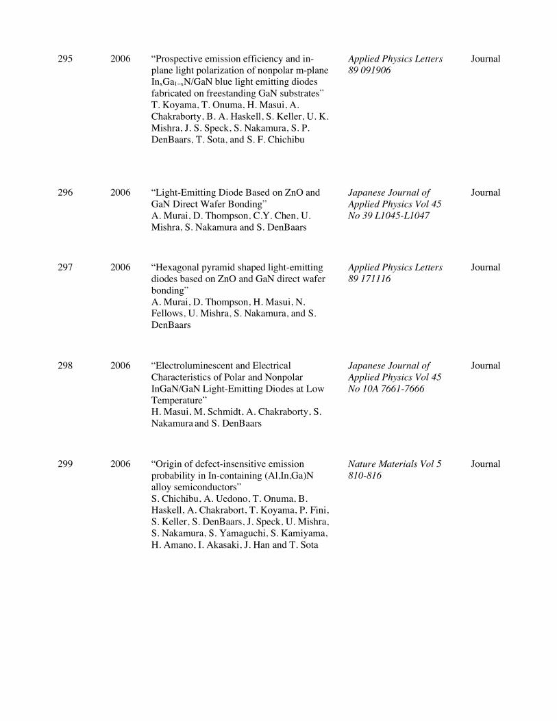
295 2006 “Prospective emission efficiency and in-plane light polarization of nonpolar m-plane InxGa1−xN/GaN blue light emitting diodes fabricated on freestanding GaN substrates” T. Koyama, T. Onuma, H. Masui, A. Chakraborty, B. A. Haskell, S. Keller, U. K. Mishra, J. S. Speck, S. Nakamura, S. P. DenBaars, T. Sota, and S. F. Chichibu
Applied Physics Letters 89 091906
Journal
296 2006 “Light-Emitting Diode Based on ZnO and GaN Direct Wafer Bonding” A. Murai, D. Thompson, C.Y. Chen, U. Mishra, S. Nakamura and S. DenBaars
Japanese Journal of Applied Physics Vol 45 No 39 L1045-L1047
Journal
297 2006 “Hexagonal pyramid shaped light-emitting diodes based on ZnO and GaN direct wafer bonding” A. Murai, D. Thompson, H. Masui, N. Fellows, U. Mishra, S. Nakamura, and S. DenBaars
Applied Physics Letters 89 171116
Journal
298 2006 “Electroluminescent and Electrical Characteristics of Polar and Nonpolar InGaN/GaN Light-Emitting Diodes at Low Temperature” H. Masui, M. Schmidt, A. Chakraborty, S. Nakamura and S. DenBaars
Japanese Journal of Applied Physics Vol 45 No 10A 7661-7666
Journal
299 2006 “Origin of defect-insensitive emission probability in In-containing (Al,In,Ga)N alloy semiconductors” S. Chichibu, A. Uedono, T. Onuma, B. Haskell, A. Chakrabort, T. Koyama, P. Fini, S. Keller, S. DenBaars, J. Speck, U. Mishra, S. Nakamura, S. Yamaguchi, S. Kamiyama, H. Amano, I. Akasaki, J. Han and T. Sota
Nature Materials Vol 5 810-816
Journal
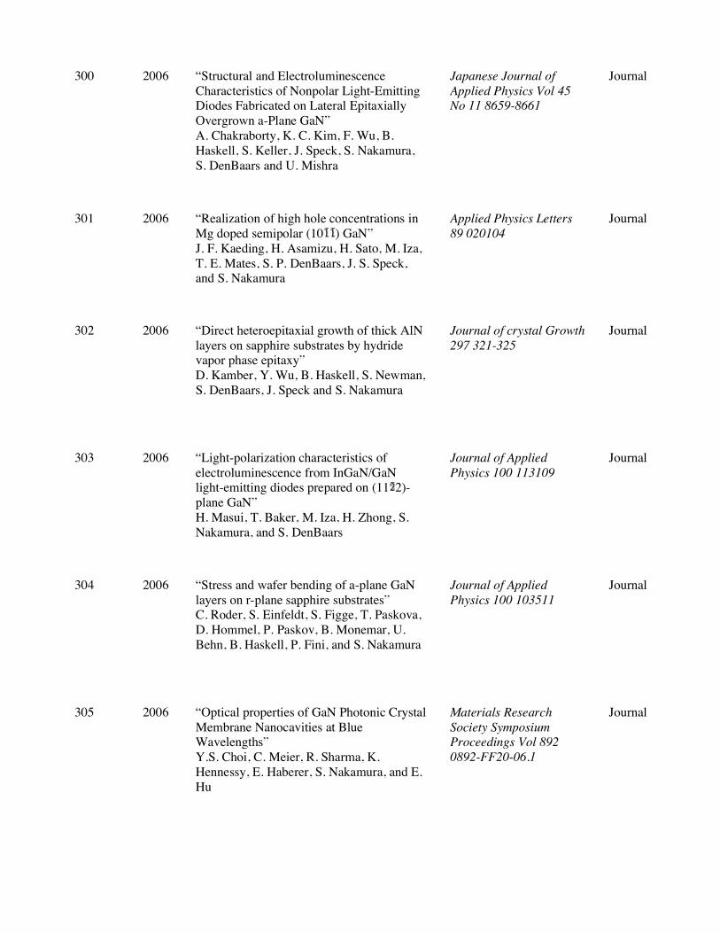
300 2006 “Structural and Electroluminescence Characteristics of Nonpolar Light-Emitting Diodes Fabricated on Lateral Epitaxially Overgrown a-Plane GaN” A. Chakraborty, K. C. Kim, F. Wu, B. Haskell, S. Keller, J. Speck, S. Nakamura, S. DenBaars and U. Mishra
Japanese Journal of Applied Physics Vol 45 No 11 8659-8661
Journal
301 2006 “Realization of high hole concentrations in Mg doped semipolar (10 ) GaN” J. F. Kaeding, H. Asamizu, H. Sato, M. Iza, T. E. Mates, S. P. DenBaars, J. S. Speck, and S. Nakamura
Applied Physics Letters 89 020104
Journal
302 2006 “Direct heteroepitaxial growth of thick AlN layers on sapphire substrates by hydride vapor phase epitaxy” D. Kamber, Y. Wu, B. Haskell, S. Newman, S. DenBaars, J. Speck and S. Nakamura
Journal of crystal Growth 297 321-325
Journal
303 2006 “Light-polarization characteristics of electroluminescence from InGaN/GaN light-emitting diodes prepared on (11 2)-plane GaN” H. Masui, T. Baker, M. Iza, H. Zhong, S. Nakamura, and S. DenBaars
Journal of Applied Physics 100 113109
Journal
304 2006 “Stress and wafer bending of a-plane GaN layers on r-plane sapphire substrates” C. Roder, S. Einfeldt, S. Figge, T. Paskova, D. Hommel, P. Paskov, B. Monemar, U. Behn, B. Haskell, P. Fini, and S. Nakamura
Journal of Applied Physics 100 103511
Journal
305 2006 “Optical properties of GaN Photonic Crystal Membrane Nanocavities at Blue Wavelengths” Y.S. Choi, C. Meier, R. Sharma, K. Hennessy, E. Haberer, S. Nakamura, and E. Hu
Materials Research Society Symposium Proceedings Vol 892 0892-FF20-06.1
Journal

306 2007 “Effect of anisotropic strain on phonons in a-plane and c-plane GaN layers” V. Darakchieva T. Paskova, M. Schubert, P. Paskov, H. Arwin, B. Monemar, D. Hommel, M. Heuken, J. Off, B. Haskell, P.T. Fini, J. Speck and S. Nakamura
Journal of Crystal Growth 300 233-238
Journal
307 2007 “Seeded Growth of GaN by the Basic Ammonothermal Method” T. Hashimoto, M. Saito, K. Fujito, F. Wu, J. Speck, S. Nakamura
Journal of Crystal Growth 305 311-316
Journal
308 2007 “Gallium-Nitride-Based Microcavity Light-Emitting Diodes with Air-Gap Distributed Bragg Reflectors” R. Sharma, Y.S. Choi, C.F. Wang, A. David, C. Weisbuch, S. Nakamura, E. Hu
Applied Physics Letters 91 211108
Journal
309 2007 “Impacts of Dislocation Bending and Impurity Incorporation on the Local Cathodoluminescence Spectra of GaN Grown by Ammonothermal Method” S. Chichibu, T. Onuma, T. Hashimoto, K. Fujito, F. Wu, J. Speck, S. Nakamura
Applied Physics Letters 91 251911
Journal
310 2007 “Relation between Al vacancies and deep emission bands in AlN epitaxial films grown by NH3-source molecular beam epitaxy” T. Koyama, M. Sugawara, T. Hoshi, A. Uedono J. Kaeding, R. Sharma, S. Nakamura, S. Chichibu
Applied Physics Letters 90 241914
Journal
311 2007 “Gallium nitride based microcavity light emitting diodes with 2λ effective cavity thickness” P. Morgan Pattison, A. David, R. Sharma, C. Weisbuch, S. DenBaars, and S. Nakamura
Applied Physics Letters 90 031111
Journal

312 2007 “Polarization anisotropy in nonpolar oriented GaN films studied by polarized photoreflectance spectroscopy” U. Behn, P. Misra, H. Grahn, B. Imer, S. Nakamura, S. DenBaars, J. Speck
Phys. Stat. Sol A 204 No 1 299-303
Journal
313 2007 “Structural and Optical Properties of Nonpolar InGaN/GaN Multiple Quantum Wells Grown on Planar and Lateral Epitaxially Overgrown m-Plane GaN Films” A. Chakraborty, B. Haskell, F. Wu, S. Keller, S. DenBaars, S. Nakamura, J. Speck, and U. Mishra
Japanese Journal of Applied Physics Vol 46 No 2 542-546
Journal
314 2007 “High Brightness Violet InGaN/GaN Light Emitting Diodes on Semipolar (1011) Bulk GaN Substrates” A. Tyagi, H. Zhong, N. Fellows, M. Iza, J. Speck, S. DenBaars, and S. Nakamura
Japanese Journal of Applied Physics Vol 46 No 7 L129-L131
Journal
315 2007 “High Power and High External Efficiency m-Plane InGaN Light Emitting Diodes” M. Schmidt, K.C. Kim, H. Sato, N. Fellows, H. Masui, S. Nakamura, S. DenBaars, and J. Speck
Japanese Journal of Applied Physics Vol 46 No 7 L126-L128
Journal
316 2007 “Room Temperature Continuous-Wave Lasing in GaN/InGaN Microdisks” A. Tamboli, E. haberer, R. Sharma, K. Lee, S. Nakamura, E. Hu
Nature Photonics Vol 1 61-64
Journal
317 2007 “Lateral epitaxial overgrowth of aluminum nitride on patterned silicon carbide substrates by hydride vapor phase epitaxy” D. Kamber, Y. Wu, E. Letts, S. DenBaars, J. Speck, S. Nakamura, and S. Newman
Applied Physics Letters 90 122116
Journal

318 2007 “Defect-mediated surface morphology of nonpolar m-plane GaN” A. Hirai, B. A. Haskell, M. B. McLaurin, F. Wu, M. C. Schmidt, K. C. Kim, T. J. Baker, S. P. DenBaars, S. Nakamura, and J. S. Speck
Applied Physics Letters 90 121119
Journal
319 2007 “Demonstration of Nonpolar m-Plane InGaN/GaN Laser Diodes” M. Schmidt, K.C. Kim, R. Farrell, D. Feezell, D. Cohen, M. Saito, K. Fujito, J. Speck, S. DenBaars, and S. Nakamura
Japanese Journal of Applied Physics Vol 46 No 9 L190-L191
Journal
320 2007 “AlGaN-Cladding-Free Nonpolar InGaN/GaN Laser Diodes” D. Feezell, M. Schmidt, R. Farrell, K.C. Kim, M. Saito, K. Fujito, D. Cohen, J. Speck, S. DenBaars, and S. Nakamura
Japanese Journal of Applied Physics Vol 46 No 13 L284-L286
Journal
321 2007 “Thin metal intracavity contact and lateral current-distribution scheme for GaN-based vertical-cavity lasers” D. F. Feezell, R. M. Farrell, M. C. Schmidt, H. Yamada, M. Ishida, S. P. DenBaars, D. A. Cohen, and S. Nakamura
Applied Physics Letters 90 181128
Journal
322 2007 “Anisotropic Strain and Phonon deformation Potentials in GaN” V. Darakchieva, T. Paskova, M. Schubert, H. Arwin, P. Paskov, B. Monemar, D. Hommel, M. Heuken, J. Off, F. Scholz, B. Haskell, J. Speck, P. Fini, S. Nakamura
Physical Review B 75 195217
Journal
323 2007 “Improved electroluminescence on nonpolar m -plane InGaN/GaN quantum wells LEDs” K.C. Kim, M. Schmidt, H. Sato, F. Wu, N. Fellows , M. Saito, K. Fujito, J. Speck, S. Nakamura, S. DenBaars
Phys Stat Sol (RRL)1 No 3 125-127
Journal
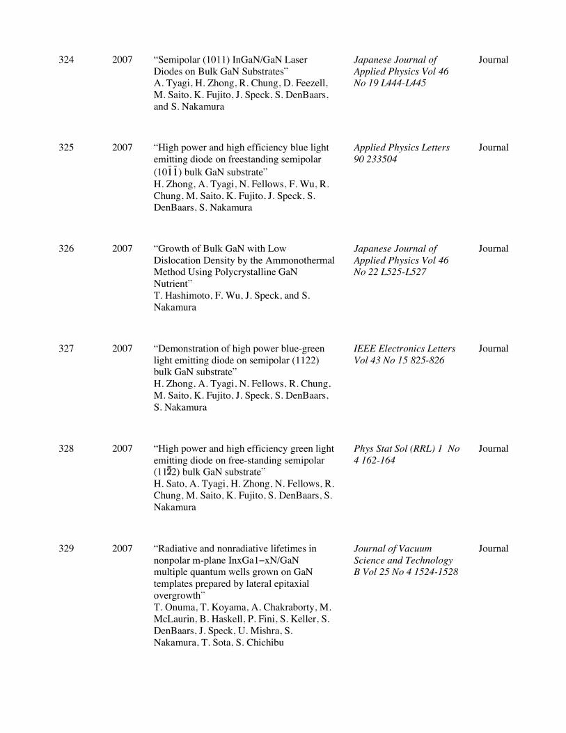
324 2007 “Semipolar (1011) InGaN/GaN Laser Diodes on Bulk GaN Substrates” A. Tyagi, H. Zhong, R. Chung, D. Feezell, M. Saito, K. Fujito, J. Speck, S. DenBaars, and S. Nakamura
Japanese Journal of Applied Physics Vol 46 No 19 L444-L445
Journal
325 2007 “High power and high efficiency blue light emitting diode on freestanding semipolar (10 ) bulk GaN substrate” H. Zhong, A. Tyagi, N. Fellows, F. Wu, R. Chung, M. Saito, K. Fujito, J. Speck, S. DenBaars, S. Nakamura
Applied Physics Letters 90 233504
Journal
326 2007 “Growth of Bulk GaN with Low Dislocation Density by the Ammonothermal Method Using Polycrystalline GaN Nutrient” T. Hashimoto, F. Wu, J. Speck, and S. Nakamura
Japanese Journal of Applied Physics Vol 46 No 22 L525-L527
Journal
327 2007 “Demonstration of high power blue-green light emitting diode on semipolar (1122) bulk GaN substrate” H. Zhong, A. Tyagi, N. Fellows, R. Chung, M. Saito, K. Fujito, J. Speck, S. DenBaars, S. Nakamura
IEEE Electronics Letters Vol 43 No 15 825-826
Journal
328 2007 “High power and high efficiency green light emitting diode on free-standing semipolar (11 2) bulk GaN substrate” H. Sato, A. Tyagi, H. Zhong, N. Fellows, R. Chung, M. Saito, K. Fujito, S. DenBaars, S. Nakamura
Phys Stat Sol (RRL) 1 No 4 162-164
Journal
329 2007 “Radiative and nonradiative lifetimes in nonpolar m-plane InxGa1−xN/GaN multiple quantum wells grown on GaN templates prepared by lateral epitaxial overgrowth” T. Onuma, T. Koyama, A. Chakraborty, M. McLaurin, B. Haskell, P. Fini, S. Keller, S. DenBaars, J. Speck, U. Mishra, S. Nakamura, T. Sota, S. Chichibu
Journal of Vacuum Science and Technology B Vol 25 No 4 1524-1528
Journal
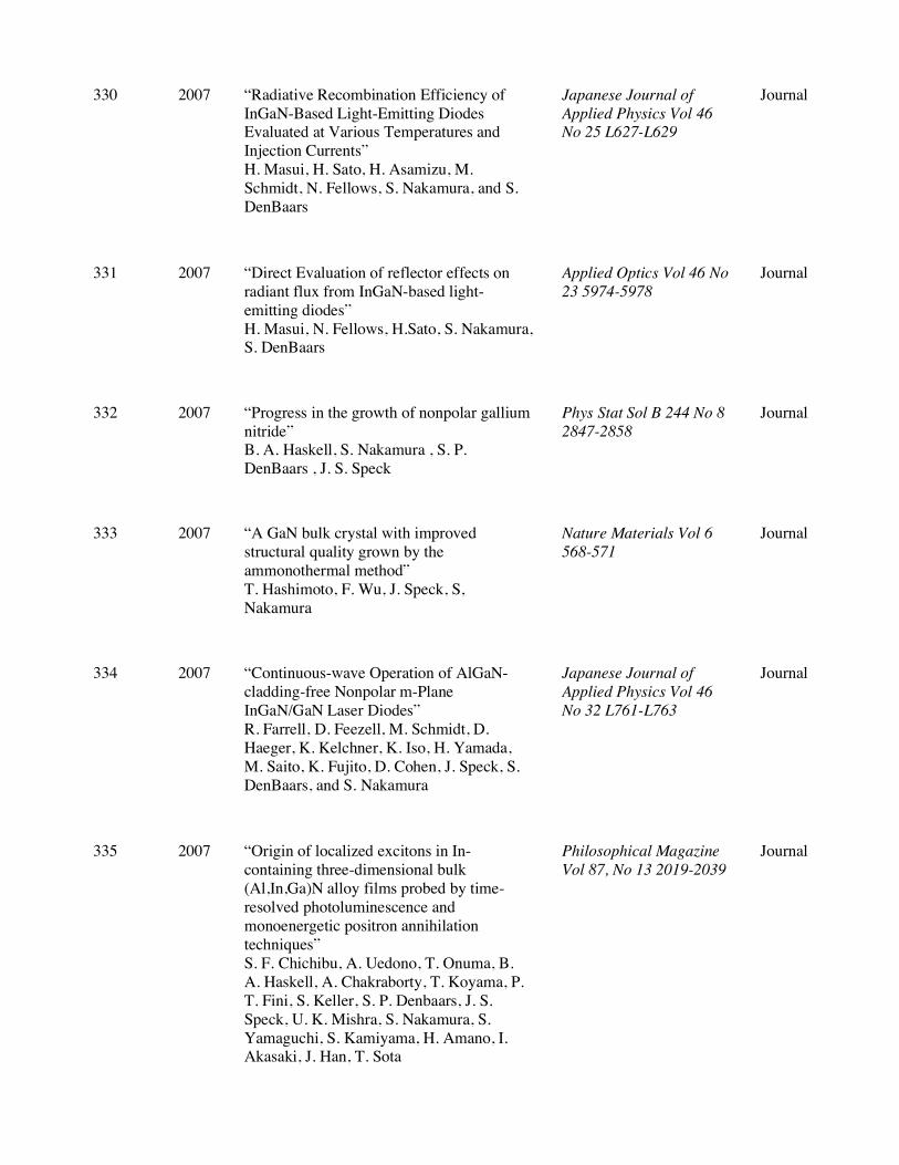
330 2007 “Radiative Recombination Efficiency of InGaN-Based Light-Emitting Diodes Evaluated at Various Temperatures and Injection Currents” H. Masui, H. Sato, H. Asamizu, M. Schmidt, N. Fellows, S. Nakamura, and S. DenBaars
Japanese Journal of Applied Physics Vol 46 No 25 L627-L629
Journal
331 2007 “Direct Evaluation of reflector effects on radiant flux from InGaN-based light-emitting diodes” H. Masui, N. Fellows, H.Sato, S. Nakamura, S. DenBaars
Applied Optics Vol 46 No 23 5974-5978
Journal
332 2007 “Progress in the growth of nonpolar gallium nitride” B. A. Haskell, S. Nakamura , S. P. DenBaars , J. S. Speck
Phys Stat Sol B 244 No 8 2847-2858
Journal
333 2007 “A GaN bulk crystal with improved structural quality grown by the ammonothermal method” T. Hashimoto, F. Wu, J. Speck, S, Nakamura
Nature Materials Vol 6 568-571
Journal
334 2007 “Continuous-wave Operation of AlGaN-cladding-free Nonpolar m-Plane InGaN/GaN Laser Diodes” R. Farrell, D. Feezell, M. Schmidt, D. Haeger, K. Kelchner, K. Iso, H. Yamada, M. Saito, K. Fujito, D. Cohen, J. Speck, S. DenBaars, and S. Nakamura
Japanese Journal of Applied Physics Vol 46 No 32 L761-L763
Journal
335 2007 “Origin of localized excitons in In-containing three-dimensional bulk (Al,In,Ga)N alloy films probed by time-resolved photoluminescence and monoenergetic positron annihilation techniques” S. F. Chichibu, A. Uedono, T. Onuma, B. A. Haskell, A. Chakraborty, T. Koyama, P. T. Fini, S. Keller, S. P. Denbaars, J. S. Speck, U. K. Mishra, S. Nakamura, S. Yamaguchi, S. Kamiyama, H. Amano, I. Akasaki, J. Han, T. Sota
Philosophical Magazine Vol 87, No 13 2019-2039
Journal
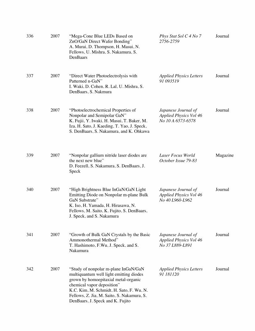
336 2007 “Mega-Cone Blue LEDs Based on ZnO/GaN Direct Wafer Bonding” A. Murai, D. Thompson, H. Masui, N. Fellows, U. Mishra, S. Nakamura, S. DenBaars
Phys Stat Sol C 4 No 7 2756-2759
Journal
337 2007 “Direct Water Photoelectrolysis with Patterned n-GaN” I. Waki, D. Cohen, R. Lal, U. Mishra, S. DenBaars, S. Nakmura
Applied Physics Letters 91 093519
Journal
338 2007 “Photoelectrochemical Properties of Nonpolar and Semipolar GaN” K. Fujii, Y. Iwaki, H. Masui, T. Baker, M. Iza, H. Sato, J. Kaeding, T. Yao, J. Speck, S. DenBaars, S. Nakamura, and K. Ohkawa
Japanese Journal of Applied Physics Vol 46 No 10 A 6573-6578
Journal
339 2007 “Nonpolar gallium nitride laser diodes are the next new blue” D. Feezell, S. Nakamura, S. DenBaars, J. Speck
Laser Focus World October Issue 79-83
Magazine
340 2007 “High Brightness Blue InGaN/GaN Light Emitting Diode on Nonpolar m-plane Bulk GaN Substrate” K. Iso, H. Yamada, H. Hirasawa, N. Fellows, M. Saito, K. Fujito, S. DenBaars, J. Speck, and S. Nakamura
Japanese Journal of Applied Physics Vol 46 No 40 L960-L962
Journal
341 2007 “Growth of Bulk GaN Crystals by the Basic Ammonothermal Method” T. Hashimoto, F.Wu, J. Speck, and S. Nakamura
Japanese Journal of Applied Physics Vol 46 No 37 L889-L891
Journal
342 2007 “Study of nonpolar m-plane InGaN/GaN multiquantum well light emitting diodes grown by homoepitaxial metal-organic chemical vapor deposition” K.C. Kim, M. Schmidt, H. Sato, F. Wu, N. Fellows, Z. Jia, M. Saito, S. Nakamura, S. DenBaars, J. Speck and K. Fujito
Applied Physics Letters 91 181120
Journal

343 2007 “Formation and reduction of pyramidal hillocks on m-plane {1100} GaN” A. Hirai, Z. Jia, M. C. Schmidt, R. M. Farrell, S. P. DenBaars, S. Nakamura, J. S. Speck, and K. Fujito
Applied Physics Letters 91 191906
Journal
344 2007 “Electrical Characteristics of Nonpolar InGaN-Based Light-Emitting Diodes Evaluated at Low Temperature” H. Masui, M. Schmidt, K. C. Kim, A. Chakraborty, S. Nakamura, and S. DenBaars
Japanese Journal of Applied Physics Vol 46 No 11 7309-7310
Journal
345 2007 “Impact of Substrate Miscut on the Characteristic of m-plane InGaN/GaN Light Emitting Diodes” H. Yamada, K. Iso, M. Saito, K. Fujito, S. DenBaars, J. Speck, and S. Nakamura
Japanese Journal of Applied Physics Vol 46 No 46 L 1117-L1119
Journal
346 2007 “Impact of strain on free-exciton resonance energies in wurtzite AlN” H. Ikeda, T. Okamura, K. Matsukawa, T. Sota, M. Sugawara, T. Hoshi, P. Cantu, R. Sharma, J. Kaeding, S. Keller, U. Mishra, K. Kosaka, K. Asai, S. Sumiya, T. Shibata, M. Tanaka, J. Speck, S. DenBaars, S. Nakamura, T. Koyama, T. Onuma, and S. Chichibu
Journal Of Applied Physics 102 123707
Journal
347 2007 “Analytical light-ray tracing in two-dimensional objects for light-extraction problems in light-emitting diodes” H. Masui, S. Nakamura, S. DenBaars
Applied Optics Vol 47 No 1 88-92
Journal
348 2007 “Recent Performance of Nonpolar and Semipolar GaN-Based Light Emitting Diodes and Laser Diodes” D. Feezell, S. DenBaars, J. Speck, S. Nakamura
Compound Semiconductor Integrated Circuit Symposium IEEE 1-4
Conference Proceeding

349 2007 “Electrical characterization of low defect density nonpolar (11 0) a-plane GaN grown with sidewall lateral epitaxial overgrowth (SLEO)” B.Imer, B. Haskell, S. Rajan, S. Keller, U. Mishra, S. Nakamura, J. Speck, S. DenBaars
Journal of Materials Research Vol 23 No 2 551-555
Journal
350 2007 “Status and Perspectives of the Ammonothermal Growth of GaN Substrates” T. Hashimoto, F. Wu, M. Saito, K. Fujito, J.Speck, S. Nakamura
Journal of Crystal Growth 310 876-880
Journal
351 2007 “Influence of Mg Doping on the Morphological, Optical, and Structural Properties of InGaN/GaN Multiple Quantum Wells” Z. Chen, N. Fichtenbaum, D. Brown, S. Keller, U.K. Mishra, S.P. Denbaars, and S. Nakamura
Journal of Electronic Materials Vol 37 No 5 546-549
Journal
352 2008 “Characterization of nanoscale electronic structure in nonpolar GaN using scanning capacitance microscopy” S. Nakamura, J. S. Speck, and S. P. DenBaars et. al
Journal of Applied Physics 103 014305
Journal
353 2008 “GaN/InGaN light emitting diodes with embedded photonic crystal obtained by lateral epitaxial overgrowth” A. David, B. Moran, K. McGroddy, E. Matioli, E. Hu, S DenBaars, S. Nakamura, and C. Weisbuch
Applied Physics Letters 92 113514
Journal
354 2008 “Comparison of InGaN/GaN light emitting diodes grown on m -plane and a -plane bulk GaN substrates” K. Fujito , J. Speck , S. DenBaars , S. Nakamura, et. al
Phys Stat Sol RRL 2 No 2 89-91
Journal
355 2008 “Compositional Dependence of Nonpolar m-Plane InxGa1-xN/GaN Light Emitting Diodes” H. Yamada, K. Iso, M. Saito, H. Masui, K. Fujito, S. DenBaars, and S. Nakamura
Applied Physics Express 1 041101
Journal
356 2008 “Optical polarization characteristics of InGaN/GaN light-emitting diodes fabricated on GaN substrates oriented between (1010) and (1011) planes” H. Masui, H. Yamada, K. Iso, S. Nakamura, and S. DenBaars
Applied Physics Letters 92 091105
Journal
357 2008 “High Power and High Efficiency Semipolar InGaN light Emitting Diodes” H. Sato, H. Hirasawa, H. Asamaizu, N. Fellows, A. Tyagi, M. Saito, K. Fujito, J. Speck, S. DenBaars, S. Nakamura
Journal of Light and Vis. Env. Vol 32 No 2 107-110
Journal
358 2008 “ZnO cone-shaped blue light emitting diodes” A. Murai, D. Thompson, U. Mishra, S. Nakamura, and S. DenBaars
Proceedings of SPIE Conferences and Symposiums Vol 6895 68950N-1-68950N-9
Conference Proceedings
359 2008 “Electroluminescence efficiency of -oriented InGaN-based light-emitting diodes at low temperature” H. Masui, H. Kroemer, M. Schmidt, K.C. Kim, N. Fellows, S. Nakamura and S. DenBaars
Journal of Physics D: Applied Physics 41 082001
Journal
360 2008 “InGaN/GaN laser diodes on semipolar (10) bulk GaN substrates”
A. Tyagi , H. Zhong , R. Chung , D. Feezell, M. Saito, K. Fujito, J. Speck , S. DenBaars , S. Nakamura
Phys Stat Sol C 5 No 6 2108-2110
Journal
361 2008 “Equivalent-Circuit Analysis for the Electroluminescence-Efficiency Problem of InGaN/GaN Light-Emitting Diodes” H. Masui, T. Ive, M. Schmidt, N. Fellows, H. Sato, H. Asamizu, S. Nakamura, and S. DenBaars
Japanese Journal of Applied Physics Vol 47 No 4 2112-2118
Journal
362 2008 “Enhancement of external quantum efficiency in GaN-based light emitting diodes using a suspended geometry” N. Fellows, H. Masui, H. Sato, H. Asamizu, M. Iza, H. Zhong, S. Nakamura, S. DenBaars
Phys Stat Sol C 5 No 6 2216-2218
Journal
363 2008 “Hexagonal Truncated Pyramidal Light Emitting Diodes through Wafer Bonding of ZnO to GaN, Laser Lift-off, and Photo Chemical Etching” D. Thompson, A. Murai, M. Iza, S. Brinkley, S. DenBaars, U. Mishra, and S. Nakamura
Japanese Journal of Applied Physics Vol 47 No 5 3447-3449
Journal
364 2008 “White X-ray microdiffraction analysis of defects, strain and tilts in a free standing GaN film” R. Barabash, G. Ice, B. Haskell, S. Nakamura , J. Speck , W. Liu
Phys Stat Sol B 245 No 5 899-902
Journal
365 2008 “Erratum: “Impact of strain on free-exciton resonance energies in wurtzite AlN” [J. Appl. Phys. 102, 123707 (2007)]” H. Ikeda, T. Okamura, K. Matsukawa, T. Sota, M. Sugawara, et al.
Journal of Applied Physics 103 089901
Journal
366 2008 “Optical polarization of m -plane In-GaN/GaN light-emitting diodes characterized via confocal microscope” H. Masui , H. Yamada, K. Iso, H. Hirasawa, N. Fellows, J. Speck, S. Nakamura, S. DenBaars
Phys Stat Sol A 205 No 5 1203-1206
Journal
367 2008 “Non-polar-oriented InGaN light-emitting diodes for liquid-crystal-display backlighting” H.Masui, H. Yamada, K. Iso, J. Speck, S. Nakmura, S. DenBaars
Journal of the Society for Information Display Volume 16, Issue 4, pp. 571-578
Journal

368 2008 “Optical polarization characteristics of light emission from sidewalls of primary-color light-emitting diodes” H. Masui, N. Fellows, S. Nakamura and S. DenBaars
Semiconductor Science and Technology 23 072001 1-4
Journal
369 2008 “Improved quality nonpolar a -plane GaN/AlGaN UV LEDs grown with sidewall lateral epitaxial overgrowth (SLEO)” B. Imer , M. Schmidt , B. Haskell , S. Rajan , B. Zhong , K.C. Kim , F. Wu , T. Mates , S. Keller , U. Mishra , S. Nakamura , J. Speck , S. DenBaars
Phys Stat Sol A 205 No 7 1705-1712
Journal
370 2008 “Experimental technique to correlate optical excitation intensities with electrical excitation intensities for semiconductor optoelectronic device characterization” H. Masui, S. Nakamura and S. DenBaars
Semiocnductor Science and Technology 23 085018
Journal
371 2008 “Electrical characterization of low defect density nonpolar (11 0) a-plane GaN grown with sidewall lateral epitaxial overgrowth (SLEO)” B. Imer, B. Haskell, S. Rajan, S. Keller, U. Mishra, S. Nakamura, J. Speck, S. DenBaars
Journal of Material Research Vol 23 No 2 551-555
Journal
372 2008 “Optical properties of yellow light-emitting diodes grown on semipolar (1122) bulk GaN substrates” H. Sato, R. Chung, H. Hirasawa, N. Fellows, H. Masui, F. Wu, M. Saito, K. Fujito, J. Speck, S. DenBaars, and S. Nakamura
Applied Physics Letters 92 221110
Journal
373 2008 “Ammonothermal Growth of Bulk GaN” T. Hashimoto, F. Wu, J. Speck, S. Nakamura
Journal of Crystal Growth 310 3907-3910
Journal

374 2008 “Quantum-confined Stark effect on photoluminescence and electroluminescence characteristics of InGaN-based light-emitting diodes” H. Masui, J. Sonoda, N. Pfaff, I. Koslow, S. Nakamura and S. DenBaars
Journal of Physics D: Applied Physics 41 165105
Journal
375 2008 “Directional emission control and increased light extraction in GaN photonic crystal light emitting diodes” K. McGroddy, A. David, E. Matioli, M. Iza, S. Nakamura, S. DenBaars, J. S. Speck, C. Weisbuch, and E. L. Hu
Applied Physics Letters 93 103502
Journal
376 2008 “Stimulated Emission at Blue-Green (480 nm) and Green (514 nm) Wavelengths from Nonpolar (m-plane) and Semipolar (1122) InGaN Multiple Quantum Well Laser Diode Structures” A. Tyagi, Y.D. Lin, D. Cohen, M. Saito, K. Fujito, J. Speck, S. DenBaars, and S. Nakamura
Applied Physics Express 1 091103
Journal
377 2008 “Demonstration of 426 nm InGaN/GaN Laser Diodes Fabricated on Free-Standing Semipolar (1122) Gallium Nitride Substrates” H. Asamizu, M. Saito, K. Fujito, J. Speck, S. DenBaars, and S. Nakamura
Applied Physics Express 1 091102
Journal
378 2008 “Dichromatic color tuning with InGaN-Based Light-Emitting Diodes” N. Fellows, H. Sato, Y.D. Lin, R. Chung, S. DenBaars, S. Nakamura
Applied Physics Letters 93 121112
Journal
379 2008 “Low extended defect density nonpolar m-plane GaN by sidewall lateral epitaxial overgrowth” K.C. Kim, M. Schmidt, F. Wu, M. McLaurin, A. Hirai, S. Nakamura, S. DenBaars, and J. Speck
Applied Physics Letters 93 142108
Journal
380 2008 “Optical polarization characteristics of m-oriented InGaN/GaN light-emitting diodes with various indium compositions in single-quantum-well structure” H. Masui, H. Yamada, K. Iso, S. Nakamura and S. DenBaars
Journal of Physics D: Applied Physics 41 225104
Journal
381 2008 “Pointed Cone Shaped Light-Emitting Diodes Based on ZnO/GaN Wafer Bonding” A. Murai, D. Thompson, H. Hirasawa, N. Fellows, S. Brinkley, C.J. Won, M. Iza, U. Mishra, S. Nakamura, and S. DenBaars
Japanese Journal of Applied Physics Vol 47 No 5 3522-3523
Journal
382 2008 “Increased Polarization Ratio on Semipolar (1122) InGaN/GaN Light-Emitting Diodes with Increasing Indium Composition” N. Fellows, H. Sato, H. Masui, S. DenBaars, and S. Nakamura
Japanese Journal of Applied Physics Vol 47 No 10 7854-7836
Journal
383 2008 “Plane Dependent Growth of GaN in Supercritical Basic Ammonia” M. Saito, D. Kamber, T. Baker, K. Fujito, S. DenBaars, J. Speck, and S. Nakamura
Applied Physics Express 1 121103
Journal
384 2008 “Effects of off-axis GaN substrates on optical properties of m-plane InGaN/GaN light-emitting diodes” H. Yamada, K. Iso, H. Masui, M. Saito, K. Fujito, S. DenBaars , S. Nakamura
Journal of Crystal Growth 310 4968-4971
Journal
385 2008 “Highly efficient broad-area blue and white light-emitting diodes on bulk GaN substrates” K. Vampola , N. Fellows , H.Masui , S. Brinkley , M. Furukawa , R. Chung , H. Sato , J. Sonoda , H. Hirasawa , M. Iza , S. DenBaars , S. Nakamura
Phys Stat Sol A 206 No 2 200-202
Journal
386 2008 “High Quality AIN Grown on SiC by Metal Organic Chemical Vapor Deposition” Z. Chen, S. Newman, D. Brown, R. Chung, S. Keller, U. Mishra, S. DenBaars, S. Nakamura
Applied Physics Letters 93 191906
Journal
387 2008 “Recent progress in nonpolar LEDs as polarized light emitters” H. Masui , M. Schmidt , N. Fellows , H. Yamada , K. Iso , J. Speck , S. Nakamura, S. DenBaars
Phys Stat Sol A 206 No 2 203-205
Journal
388 2009 “Effect of Indium on the Physical Vapor Transport Growth of AIN” E. Letts, J. Speck, S. Nakamura
Journal of Crystal Growth 311 1060-1064
Journal
389 2009 “The Dawn of Miniature Green Lasers” S. Nakamura, M. Riordan
Scientific American Vol. 300 No 4
Journal
390 2009 “Current Status of GaN-Based Solid-State Lighting” S. Nakamura
MRS Bulletin Vol 34 101-107
Journal
391 2009 “Evaluation of GaN substrates grown in supercritical basic ammonia” M. Saito, H. Yamada, K. Iso, H. Sato, H. Hirasawa, D. Kamber, T., S. DenBaars, J. Speck, and S. Nakamura
Applied Physics Letters 94 052109
Journal
392 2009 “Measurement of electron overflow in 450 nm InGaN light-emitting diode structures” K. Vampola, M. Iza, S. Keller, S. DenBaars, S. Nakamura
Applied Physics Letters 94 061116
Journal
393 2009 “Continuous-Wave Operation of InGaN/GaN Laser Diodes on Semipolar (1 12 2) Plane Gallium Nitrides” H. Asamizu, M. Saito, K. Fujito, J. Speck, S. DenBaars, S. Nakamura
Applied Physics Express 2 021002
Journal

394 2009 “Comparison of time-resolved photoluminescence from InGaN single quantum wells grown on nonpolar and semipolar bulk GaN substrates” G. Garrett, H. Shen, M. Wraback, A. Tyagi, M. Schmidt, J. Speck, S. DenBaars, S. Nakamaura
Phys Stat Sol C 6 No S2 S800-S803
Journal
395 2009 “Vacancy-oxygen complexes and their optical properties in AlN epitaxial films studied by positron annihilation” A. Uedono, S. Ishibashi, S. Keller, C. Moe P. Cantu, T. M. Katona, D. S. Kamber, Y. Wu, E. Letts, S. Newman, S. Nakamura, J. Speck, U. Mishra, S. DenBaars, T. Onuma, S. Chichibu
Journal of Applied Physics 105 054501
Journal
396 2009 “Enhancing the Light Extraction Efficiency of Blue Semipolar (10 ) Nitride-Based Light Emitting Diodes through Surface Patterning” H. Zhong, A. Tyagi, N. Pfaff, M. Saito, K. Fujito, J. Speck, S. DenBaars, and S. Nakamura
Japanese Journal of Applied Physics 48 030201
Journal
397 2009 “Growth of AlGaN/GaN heterojunction field effect transistors on semi-insulating GaN using an AlGaN interlayer” Z. Chen, Y. Pei, S. Newman, R. Chu, D. Brown, R. Chung, S. Keller, S. Denbaars, S. Nakamura, U. Mishra
Applied Physics Letters 94 113108
Journal
398 2009 “Lateral epitaxial overgrowth of (0001) AlN on patterned sapphire using hydride vapor phase epitaxy” S. Newman, D. Kamber, T. Baker, Y. Wu, F. Wu, Z. Chen, S. Nakamura, J. Speck, S. DenBaars
Applied Physics Letters 94 121906
Journal
399 2009 “Prospects for LED Lighting” S. Pimputkar, J. Speck, S. DenBaars, S. Nakamura
Nature Photonics Vol.3 180-182
Journal
400 2009 “Geometrical Characteristics and Surface Polarity of Inclined Crystallographic Planes of the Wurtzite and Zincblende Structures” H. Masui, S. Cruz, S. Nakamura, S. DenBaars
Journal of Electronic Materials Vol 38 No 6 756-760
Journal
401 2009 “Photoelectrochemical etching of p-type GaN heterostructures” A. Tamboli, A. Hirai, S. Nakamura, S. DenBaars, E. Hu
Applied Physics Letters 94 15113
Journal
402 2009 “Growth of AlGaN/GaN/AlGaN double heterojunction field-effect transistors and the observation of a compositional pulling effect” Z. Chen, Y. Pei, S. Newman, D. Brown, R. Chung, S. Keller, S. P. Denbaars, S. Nakamura, U. Mishra
Appliec Physics Letters 94 171117
Journal
403 2009 “Nonpolar and Semipolar Group III Nitride-Based Materials” J. Speck, S. Chichibu, et.al.
MRS Bulletin Vol 34 304-312
Journal
404 2009 “Development of Nonpolar and Semipolar InGaN/GaN Visible Light-Emitting Diodes” D. Feexell, M. Schmidt, S. DenBaars, S. Nakamura
MRS Bulletin Vol 34 318-323
Journal
405 2009 “Effects of piezoelectric fields on optoelectronic properties of InGaN/GaN quantum-well light-emitting diodes prepared on nonpolar (1 0 10) and semipolar (1 1 22) orientations” H. Masui, H. Asamizu, T. Melo, H. Yamada, K. Iso, S. Cruz, S. Nakamura, S. DanBaars
Journal of Physics D: Applied Physics 42 135106
Journal
406 2009 “Determination of polarization field in a semipolar (11 2) InGa/GaN single quantum well using Franz–Keldysh oscillations in electroreflectance” H. Shen, M. Wraback, H. Zhong, A. Tyagi, S. P. DenBaars, S. Nakamura, and J. S. Speck
Applied Physics Letters 94 241906
Journal
407 2009 “Nonpolar AlGaN-Cladding-Free Blue Laser Diodes with InGaN Waveguiding” K. Kelchner, M. Hardy, R. Ferrell, D. Haeger, F. Wu et. al
Applied Physics Express 2 071003
Journal
408 2009 “Correlation between Optical Polarization and Luminescence Morphology of (1122)-Oriented InGaN/GaN Quantum-Well Structures” H. Masui, H. Asamizu, A.Tyagi, N. Fellows, S. Nakamura, S. DenBaars
Applied Physics Express 2 071002
Journal
409 2009 “Characterization of blue-green m-plane InGaN light emitting diodes” Y.D.Lin, A. Chakraborty, S. Brinkley, H. C. Kuo, T. Melo, K. Fujito, J. Speck, S. DenBaars, S. Nakamura
Applied Physics Letters 94 261108
Journal
410 2009 “Luminescence Characteristics of N-Polar GaN and InGaN Films Grown by Metal Organic Chemical Vapor Deposition” H. Masui, S. Keller, N. Fellows, N. Fichtenbaum, M. Furukawa, S. Nakamura, U. Mishra, S. DenBaars
Japanese Journal of Applied Physics 48 071003
Journal
411 2009 “Unambiguous evidence of the existence of polarization field crossover in a semipolar InGaN/GaN single quantum well” H. Shen, M. Wraback, H. Zhong, A. Tyagi, S. P. DenBaars, S. Nakamura, J. S. Speck
Applied Physics Letters 95 033503
Journal
412 2009 “Blue-Green InGaN/GaN Laser Diodes on Miscut m-Plane GaN Substrate” Y.D. Lin, M. Hardy, K. Kelchner, D. Haeger et. al.
Applied Physics Express 2 082102
Journal
413 2009 “m-plane pure blue laser diodes with p-GaN/n-AlGaN-based asymmetric cladding and InGaN-based wave-guiding layers” Y-D. Lin, C. Y. Huang, M. Hardy, P. S. Hsu, K. Fujito, A. Chakraborty, H. Ohta, J. Speck, S. DenBaars, S. Nakamura
Applied Physics Letters 95 081110
Journal
414 2009 “Universality of bias- and temperature-induced dephasing in ballistic electronic interferometers” Y. Yamauchi, M. hashisaka, S. Nakamura, K. Chida, S. Kasai, T. Ono, R. Leturcq, K. Ensslin, D. Driscoll, A. Gossard, K. Kobyashi
Physical Review B 79 161306(R)
Journal
415 2009 “Customized Filter Cube in Fluorescence Microscope Measurements of InGaN/GaN Quantum-Well Characterization” H. Masui, J. Sonoda, A. Chakraborty, H. Yamada, K. Iso, N. Pfaff, I. Koslow, S. Nakamura, S. DenBaars
Japanese Journal of Applied Physics 48 098003
Journal
416 2009 “Effects of Growth Temperature and Postgrowth Annealing on Inhomogeneous Luminescence Characteristics of Green-Emitting InGaN Films” H. Masui, T. Melo, J. Sonoda, C. Weisbuch, S. Nakamura, S. DenBaars
Journal of Electronical Materials Vol 39 No 1 15-19
Journal
417 2009 “GaN-Based Integrated Lateral Thermoelectric Device for Micro-Power Generation” A. Sztein, H. Ohta, J. Sonoda, A Ramu, J. Bowers, S. DenBaars, S. Nakamura
Applied Physcis Letters 2 111003
Journal
418 2009 “Substitution of oxygen by fluorine in the GdSr2AlO5:Ce3+ phosphors: Gd1−xSr2+xAlO5−xFx solid solutions for solid state white lighting” W.B. Im, Y. Fourr´e, S. Brinkley, J. Sonoda, S. Nakamura, S. DenBaars, R. Seshadri
Optics Express Vol 17 No 25 22673-22679
Journal
419 2009 “Spontaneous formation of {1 01} InGaN quantum wells on a (11 2) GaN template and their electroluminescence characteristics” H. Masui , D. Kamber, M. Iza , J. Speck , S. Nakamura and S DenBaars, et. al
Semiconductor Science and Technology 25 015003
Journal
420 2009 “m-Plane GaN-Based Blue Superluminescent Diodes Fabricated Using Selective Chemical Wet Etching” M. Hardy, K. Kelchner, K. Fujito, J. Speck, S. Nakamura, S. DenBaars et. al
Applied Physics Express 2 121004
Journal
421 2009 “Partial strain relaxation via misfit dislocation generation at heterointerfaces in (Al,In)GaN epitaxial layers grown on semipolar (11 2) GaN free standing substrates” A. Tyagi, F. Wu, E. Young, H. Ohta, S. DenBaars, et al
Applied Physics Letters 95 251905
Journal
422 2009 “AlGaN-Cladding Free Green Semipolar GaN Based Laser Diode with a Lasing Wavelength of 506.4 nm” A. Tyagi, R. Ferrell, K. Kelchner, D. Haeger et. al
Applied Physics Express 3 011002
Journal
423 2009 “Non-equilibrium dephasing in ballistic interferometers” Y. Yamauchi, M. Hashisaka, S. Nakamura, K. Chida, S. Kasai, T. Ono, R. Leturcq, D. Driscoll, A. Gossard, K. Kobayashi
Journal of Physics: Conference Series 193 012045
Journal
424 2010 “State-of-the-art continuous-wave InGaN laser diodes in the violet, blue, and green wavelength regimes” J. Raring, E. Hall, M. Schmidt, C. Poblenz, B. Li, N. Pfister, D. Kebort, Y. C. Chang, D. Feezell, R. Craig, J. Speck, S. DenBaars, S. Nakamura
Proceedings of SPIE Conferences and Symposiums Vol 7686 76860L-1-76860L-10
Journal
425 2010 “High-power high-efficiency continuous-wave InGaN laser diodes in the violet, blue, and green wavelength regimes” J. Raring, E. Hall, M. Schmidt, C. Poblenz, B. Li, N. Pfister, D. Kebort, Y. C. Chang, D. Feezell, R. Craig, J. Speck, S. DenBaars, S. Nakamura
Proceedings of SPIE Conferences and Symposiums Vol 7602 760218-1-760818-10
Journal
426 2010 “Nonpolar and Semipolar III-Nitride Light-Emitting Diodes: Achievements and Challenges” H. Masui, S. Nakamura, S. DenBaars, U. Mishra
IEEE Transactions on Electron Devices Vol 57 No 1 88-100
Journal
427 2010 “Propagation of Spontaneous Emission in Birefringent m-Axis Oriented Semipolar (1122) (Al,In,Ga)N Waveguide Structures” C.Y. Huang, A. Tyagi, Y.D. Lin, M. Hardy, P.S. Hsu, K. Fujito, J.S. Ha, H. Ohta, J. Speck, S. DenBaars, S. Nakamura
Japanese Journal of Applied Physics 49 010207
Journal
428 2010 “Lattice Tilt and Misfit Dislocations in (1122) Semipolar GaN Heteroepitaxy” E. Young, F. Wu, A. Romanov, A. Tyagi, C. Gallinat, S. DenBaars, S. Nakamura, S. Speck
Applied Physics Express 3 011004
Journal
429 2010 “Optical waveguide simulations for the optimization of InGaN-based green laser diodes” C. Y. Huang, Y. D. Lin, A Tyagi, A. Chakraborty, H. Ohta, J. Speck, S. DenBaars, S. Nakamura
Journal of Applied Physics 107 023101
Journal
430 2010 “Nonequilibrium Fluctuation relations in a Quantum Coherent Conductor” S. Nakamura, Y. Yamauchi, M. Hashisaka, K. Chida, K. Kobyashi, T. Ono, R. Leturcq, K. Ensslin, K. Saito, Y. Utsumi, A. Gossard
The American Physical Society: Physical Review Letters 104 080602
Journal
431 2010 “Technique to evaluate the diode ideality factor of light-emitting diodes” H. Masui, S. Nakamura, S. DenBaars
Applied Physics Letters 96 073509
Journal
432 2010 “Photoluminescence and positron annihilation studies on Mg-doped nitrogen-polarity semipolar (1011) GaN heteroepitaxial layers grown by metalorganic vapor phase epitaxy” T. Onuma, A. Uedono, H. Asamizu, H. Sato, J. Kaeding, M. Iza, S. DenBaars, S. Nakamura, S. Chichibu
Applied Physics Letters 96 091913
Journal
433 2010 “InGaN/GaN Blue Laser Diode Grown on Semipolar (3031) Free-Standing GaN Substrates” P.S. Hsu, K. Kelchner, A. Tyagi, R. Ferrell, D. Haeger, K. Fujito, H. Ohta, S. DenBaars, J. Speck, S. Nakamura
Applied Physics Express 3 052702
Journal
434 2010 “Low-threshold-current-density AlGaN-cladding-free m-plane InGaN/GaN laser diodes” R. Farrell, P. S. Hsu, D. Hager, K. Fujito, S. DenBaars, S. Nakamura, J. Speck
Applied Physics Letters 96 231113
Journal
435 2010 “Origin of pyramidal hillocks on GaN thin films grown on free-standing m-plane GaN substrates” R. Farrell, D. Haeger, X. Chen, C. Gallinat, R. Davis, M. Cornish, K. Fujito, S. Keller, S. DenBaars, S. Nakamura, J. Speck
Applied Physics Express 96 231907
Journal
436 2010 “Stacking fault formation in the long wavelength InGaN/GaN multiple quantum wells grown on m-plane GaN” F. Wu, y.D. Lin, A. Chakraborty, H. Otha, S. DenBaars, S. Nakamura, J. Speck
Applied Physics Letters 96 231912
Journal
437 2010 “Dynamics of polarized photoluminescence in m-plane InGaN/GaN quantum wells” V. Liuolia, S. Marcinkevicius, Y. Lin, H. Ohta, S. DenBaars, S. Nakamura
Journal of Applied Physics 108, 023101
Journal
438 2010 “Vertical Stand Transparent Light-Emitting Diode Architecture for High-Efficiency and High-Power Light-Emitting Diodes” C. Pan, I. Koslow, J. Sonoda, H. Ohta, J. Ha, S. Nakamura, S. DenBaars
Japanese Journal of Applied Physics 49, 080210
Journal
439 2010 “High Power and High Efficiency Blue InGaN Light Emitting Diodes on Free-Standing Semipolar (30(3)over-bar(1)over-bar) Bulk GaN Substrate” I. Koslow, J. Sonoda, R. Chung, C. Pan, S. Brinkley, H. Ohta, S. Nakamura, S. DenBaars
Japanese Journal of Applied Physics 49, 080203
Journal
440 2010 “High Quality InGaN/AlGaN Multiple Quantum Wells for Semipolar InGaN Green Laser Diodes” Y. Lin, S. Yamamoto, C. Huang, C. Hsiung, F. Wu, K. Fujito, H. Ohta, J. Speck, S. DenBaars, S. Nakamura
Applied Physics Express 3, 082001
Journal
441 2010 “Carrier localization in m-plane InGaN/GaN quantum wells probed by scanning near field optical spectroscopy” V. Liuolia, A. Pinos, S. Marcinkevičius, Y. D. Lin, H. Ohta, S. P. DenBaars, and S. Nakamura
Applied Physics Letters 97, 151106
Journal
442 2010 “Future of group-III nitride semiconductor green laser diodes [Invited]” H. Ohta, S. DenBaars, Shuji Nakamura
Journal of Optical Society of America-B, Optical Physics 27, Issue 11
Journal

443 2010 “Effect of carrier gas and substrate misorientation on the structural and optical properties of m-plane InGaN/GaN light-emitting diodes” R. Farrell, D. Haeger, X. Chen, M. Iza, A. Hirai, K. Kelchner, K. Fujito, A. Chakraborty, S. Keller, S. DenBaars, J. Speck, S. Nakamura
Journal of Crystal Growth 313, 1-7
Journal
444 2011 “Aluminum nitride grown on lens shaped patterned sapphire by hydride vapor phase epitaxy” B. Bryant, D. Kamber, F. Wu, S. Nakamura, J. S. Speck
Physica Status Solidi C 8, Issue 5
Journal
445 2011 “Blue InGaN/GaN laser diodes grown on (3031) free-standing GaN substrates” P. S. Hsu, J. Sonoda, K. Kelchner, A. Tyagi, R. Farrell, D. Haeger, E. Young, A. Romanov, K. Fujito, H. Ohta, S. P. DenBaars, J. Speck, S. Nakamura
Physica Status Solidi C 8, Issue 7-8, 2390-2392
Journal
446 2011 “Effect of n-AlGaN cleave assistance layers on the morphology of c-plane cleaved facets for m-plane InGaN/GaN laser diodes” M. T. Hardy, R. M. Farrell, P. S. Hsu, D. A. Haeger, K. Kelchner, K. Fujito, A. Chakraborty, D. A. Cohen, S. Nakamura, J. S. Speck, S. P. DenBaars
Physica Status Solidi C 8, Issue 7-8, 2226-2228
Journal
447 2011 “Polarized spontaneous emission from blue-green m-plane GaN-based light emitting diodes” S. Brinkley, Y. Lin, A. Chakraborty, N. Pfaff, D. Cohen, J. Speck, S. Nakamura, and S. DenBaars
Applied Physics Letters 98, Issue 1, 011110
Journal
448 2011 “High internal and external quantum efficiency InGaN/GaN solar cells” E. Matioli, C. Neufeld, M. Iza, S. Cruz, A. Al-Heji, X. Chen, R. Farrell, S. Keller, S. DenBaars, U. Mishra, S. Nakamura, J. Speck, and C. Weisbuch
Applied Physics Letters 98, Issue 2, 021102
Journal
449 2011 “Misfit dislocation formation at heterointerfaces in (Al,In) GaN heteroepitaxial layers grown on semipolar free-standing GaN substrates” F. Wu, A. Tyagi, E. Young, A. Romanov, K. Fujito, S. DenBaars, S. Nakamura, J. Speck
Journal of Applied Phyics 109, Issue 3
Journal
450 2011 “Ohmic Cathode Electrode on the Backside of m-Plane and (20(2)over-bar1) Bulk GaN Substrates for Optical Device Applications” C. Hsiung, Y. Lin, H. Ohta, S. DenBaars, S. Nakamura
Japanese Journal of Applied Physics 50, Issue 3, 030208
Journal
451 2011 “Droop improvement in high current range on PSS-LEDs” S. Tanaka, Y. Zhao, I. Koslow, C. Pan, H-T. Chen, J. Sonoda, S. DenBaars, S. Nakamura
Electronics Letters 47, Issue 5 pg. 335-U66
Journal
452 2011 “Fluctuation theorem and microreversibility in a quantum coherent conductor” S. Nakamura, Y. Yamauchi, M. Hashisaka, K. Chida, K. Kobayashi, T. Ono, R. Leturcq, K. Ensslin, K. Saito, Y. Utsumi, A. Gossard
Physical Review B 83, 155431
Journal
453 2011 “Electroluminescence enhancement of (11(2)over-bar2) semipolar GaN light-emitting diodes grown on miscut m-plane sapphire substrates” S. Bae, D. Lee, B. Kong, H. Cho, J. Kaeding, S. Nakamura, S. DenBaars, J. Speck
Current Applied Physics 98, 954-958
Journal
454 2011 “Atom probe analysis of interfacial abruptness and clustering within a single In(x)Ga(1-x)N quantum well device on semipolar, (10(11)(--)) GaN substrate” T. Prosa, P. Clifton, H. Zhong, A. Tyagi, R. Shivaraman, S. DenBaars, S. Nakamura, and J. Speck
Applied Physics Letters 98, Issue 19 191903
Journal
455 2011 “Basal plane misfit dislocations and stress relaxation in III-nitride semipolar heteroepitaxy” A. Romanov, E. Young, F. Wu, A. Tyagi, C. Gallinat, S. Nakamura, S. DenBaars, J. Speck
Journal of Applied Physics 109, Issue 10, 103522
Journal
456 2011 “High quantum efficiency InGaN/GaN multiple quantum well solar cells with spectral response extending out to 520 nm” R. Farrell, C. Neufeld, S. Cruz, J. Lang, M. Iza, S. Keller, S. Nakamura, S. DenBaars, U. Mishra, and J. Speck
Applied Physics Letters 98, Issue 20, 201107
Journal
457 2011 “Growth study and impurity characterization of AlxIn1−xN grown by metal organic chemical vapor deposition” R. Chung, F. Wu, Ravi Shivaraman, S. Keller, S. DenBaars, J. Speck, and S. Nakamura
Journal of Crystal Growth 324, Issue 1 Pg 163-167
Journal
458 2011 “Erratum: Atom probe analysis of interfacial abruptness and clustering within a single In x Ga 1 x N quantum well device on semipolar (10 1¯1¯) GaN substrate” T. J. Prosa, P. H. Clinton, H. Zhong, A. Tyagi, R. Shivaraman, S. P. DenBaars, S. Nakamura, J. S. Speck
Applied Physics Letters 98, 239901
Journal
459 2011 “Effect of doping and polarization on carrier collection in InGaN quantum well solar cells” C. Neufeld, S. Cruz, R. Farrell, Michael Iza, J. Lang, S. Keller, S. Nakamura, S. DenBaars, J. Speck, U. Mishra
Applied Physics Letters 98, Issue 24, 243507
Journal
460 2011 “Polarized light extraction in m-plane GaN light-emitting diodes by embedded photonic-crystals” E. Matioli, S. Brinkley, K. Kelchner, S. Nakamura, S. DenBaars, J. Speck, C. Weisbuch
Applied Physics Letters 98, Issue 25, 251112
Journal
461 2011 “High-Power Blue-Violet Semipolar (20(2)over-bar(1)over-bar) InGaN/GaN Light-Emitting Diodes with Low Efficiency Droop at 200 A/cm(2)” Y. Zhao, S. Tanaka, CC Pan, K. Fujito, D. Feezell, JS Speck, SP DenBaars, S. Nakamura
Applied Physics Express, 4, Issue 8, 082104
Journal
462 2011 “High Optical polarization ratio from semipolar (20(2)over-bar(1)over-bar) blue-green InGaN/GaN light-emitting diodes” Y. Zhao, S. Tanaka, Q. Yan, C. Huang, R. Chung, C. Pan, K. Fujito, D. Feezell, C. Van de Walle, J. Speck, S. DenBaars, S. Nakamura
Applied Physics Letters 99, Issue 5, 051109
Journal
463 2011 “Observation of positive thermal power coefficient in InGaN/GaN quantum well solar cells” CJ. Neufeld, SC. Cruz, RM Farrell, M. Iza, S. Keller, S. Nakamura, SP DenBaars, JS Speck, UK Mishra
Applied Physics Letters, 99, Issue 7, 071104
Journal
464 2011 “Misfit dislocation formation via pre-existing threading dislocation glide in (11(2)over-bar2) semipolar heteroepitaxy” PS Hsu, EC Young, AE Romanov, K. Fujito, SP DenBaars, S. Nakamura, JS Speck
Applied Physics Letters, 99, Issue 8, 081912
Journal
465 2011 “Group III-nitride lasers: a materials perspective” MT Hardy, DF Feezell, SP DenBaars, S. Nakamura
Materials Today, 14, Issue 9, 408-415
Journal
466 2011 “AlGaN-Cladding-Free m-Plane InGaN/GaN Laser Diodes with p- Type AlGaN Etch Stop Layers” RM Farrell, DA Haeger, PS Hsu, MT Hardy, K. Kelchner, K. Fujito, D. Feezell, U. Mishra, S. DenBaars, J. Speck, S. Nakamura
Applied Physics Express, 4, Issue 9, 092105
Journal
467 2011 “Temperature Dependent Capacitance-Voltage Analysis of Uninentionally Doped and Si Doped AI0.82ln0.18N Grown on GaN” R. Chung, O. Bierwagen, F. Wu, S. Keller, S. DenBaars, J. Speck, S. Nakamura
Japanese Journal of Applied Physics, 50, Issue 10, 101001
Journal
468 2011 “Influence of Mg-doped barriers on semipolar (20(2)over-bar1) multiple-quantum-well green light-emitting diodes” C. Huang, Q. Yan, Y. Zhao, K. Fujito, D. Feezell, C. Van de Walle, J. Speck, S. DenBaars, S. Nakamura
Applied Physics Letters, 99, Issue 14, 141114
Journal
469 2011 “Determination of internal parameters for AlGaN-cladding-free m-plane InGaN/GaN laser diodes” R. Farrell, D. Haeger, P. Hsu, K. Fujito, D. Feezell, S. DenBaars, J. Speck, S. Nakamura
Applied Physics Letters, 99, Issue 17, 171115
Journal
470 2011 “High-power blue-violet AlGaN-cladding-free m-plane InGaN/GaN laser diodes” R. Farrell, D. Haeger, P. Hsu, M. Schmidt, K. Fujito, D. Feezell, S. DenBaars, J. Speck, S. Nakamura
Applied Physics Letter, 99, Issue 17, 171113
Journal
471 2011 “High optical polarization ratio from semipolar (2021) blue-green InGaN/GaN light-emitting diodes” Y. Zhao, S. Tanaka, Q. Yan, C. Huang, R. Chung, C. Pan, K. Fujito, D. Feezell, C. Van de Walle, J. Speck, S. DenBaars, S. Nakamura
Applied Physics Letters, 99, Issue 22, 229902
Journal

472 2011 “Demonstration of 505 nm laser diodes using wavelength-stable semipolar (20(21)over-bar) InGaN/GaN quantum wells” C. Huang, M. Hardy, K. Fujito, D. Feezell, J. Speck, S. DenBaars, S. Nakamura
Applied Physics Letters, 99, Issue 24, 241115
Journal
473 2011 “Robust thermal performance of Sr2Si5N8:Eu2+: An efficient red emitting phosphor for light emitting diode based white lighting” S. Brinkley, N. Pfaff, K. Denault, Z. Zhang, H. Hintzen, R. Seshadri, S. Nakamura, and S. DenBaars
Applied Physics Letters, 99, Issue 24, 241106
Journal
474 2011 “High temperature thermoelectric properties of optimized InGaN” A. Sztein, H. Ohta, J. Bowers, S. DenBaars, S. Nakamura
Journal of Applied Physics, 110, Issue 12, 123709
Journal
475 2011 “Observation of non-basal slip in semipolar InxGa1-xN/GaN heterostructures” F. Wu, E. Young, I. Koslow, M. Hardy, P. Hsu, A. Romanov, S. Nakamura, S. DenBaars, J. Speck
Applied Physics Letters, 99, Issue 25, 251909
Journal
476 2012 “Advances in GaN Semiconductors for Energy Efficient Solid State Lighting, SP DenBaars, CC Pan, N. Pfaff, S. Tanaka, JS Speck, S Nakamura
2012 IEEE Photonics Conference, 427-428
Refereed Proceeding
477 2012 “Semipolar (20(2)over-bar(1)over-bar) Blue and Green InGaN Light-Emitting Diodes” YJ Zhao, CY Huang, S. Tanaka, CC Pan, K Fujito, D Feezell, JS Speck, SP DenBaars, S. Nakamura
Conference on Lasers and Electro-Optics
Refereed Proceeding
478 2012 “High light extraction efficiency light-emitting diodes grown on bulk GaN and sapphire substrates using vertical transparent package” CC Pan, S. Nakamura, SP DenBaars
Conference on Lasers and Electro-Optics
Refereed Proceeding

479 2012 “Semipolar (20(21)over-bar) Laser Diodes (lambda=505nm) with Wavelength-Stable InGaN/GaN Quantum Wells” CY Huang, Y. Zhao, MT Hardy, K. Fujito, DF Feezell, JS Speck, SP DenBaars, S. Nakamura
Conference on Lasers and Electro-Optics
Refereed Proceeding
480 2012 “Demonstration of a Relaxed Waveguide Semipolar (20(2)over-bar1) InGaN/GaN Laser Diode” MT Hardy, PS Hsu, I Koslow, DF Feezell, S. Nakamura, JS Speck, SP DenBaars
Conference on Lasers and Electro-Optics
Refereed Proceeding
481 2012 “384 nm AlGaN Diode Lasers on Relaxed Semipolar Buffers” DA Haeger, EC Young, RB Chung, F Wu, AE Romanov, S Nakamura, SP DenBaars, JS Speck, DA Cohen
Conference on Lasers and Electro-Optics
Refereed Proceeding
482 2012 “Latest Performance of GaN-based Nonpolar.Semipolar Emitting Devices” S. Nakamura
IEEE International Semiconductor Laser Conference
Refereed Proceeding
483 2012 “High efficiency white LEDs with single-crystal ZnO current spreading layers deposited by aqueous solution epitaxy” A. Reading, J. Richardson, C. Pan, S. Nakamura, and S. DenBaars
Optics Express, 20, Issue 1, A13-A19
Journal
484 2012 “444.9 nm semipolar (11(2)over-bar2) laser diode grown on an intentionally stress relaxed InGaN waveguiding layer” P. Hsu, M. Hardy, F. Wu, I. Koslow, E. Young, A. Romanov, K. Fujito, D. Feezell, S. DenBaars, J. Speck, S. Nakamura
Applied Physics Letters, 100, Issue 2, 021104
Journal
485 2012 “Assessment of deep level defects in m-plane GaN grown by metalorganic chemical vapor deposition” T. Henry, A. Armstrong, K. Kelchner, S. Nakamura, S. DenBaars, J. Speck
Applied Physics Letters, 100, Issue 8 082103
Journal
486 2012 “The polarization field dependence of Ti/Al based Ohmic contacts on N-type semipolar GaN” R. Chung, H. Chen, C. Pan, J. Ha, S. DenBaars, S. Nakamura
Applied Physics Letters, 100, Issue 9 091104
Journal
487 2012 “Chip Shaping for Light Extraction Enhancement of Bulk c-Plane Light-Emitting Diodes” S. Brinkley, C. Keraly, J. Sonoda, C. Weisbuch, J. Speck, S. Nakamura, S. DenBaars
Applied Physics Express, 5, Issue 3 032104
Journal
488 2012 “Effect of quantum well cap layer thickness on the microstructure and performance of InGaN/GaN solar cells” Y. Hu, R. Farrell, C. Neufeld, M. Iza, S. Cruz, N. Pfaff, D. Simeonov, S. Keller, S. Nakamura, S. DenBaars, U. Mishra, and J. Speck
Applied Physics Letters, 100, Issue 16 161101
Journal
489 2012 “384 nm laser diode grown on a (20(2)over-bar1) semipolar relaxed AlGaN buffer layer” D. Haeger, E. Young, R. Chung, F. Wu, N. Pfaff, M. Tsai, K. Fujito, S. DenBaars, J. Speck, S. Nakamura, D. Cohen
Applied Physics Letters, 100, Issue 16 161107
Journal
490 2012 “Double embedded photonic crystals for extraction of guided light in light-emitting diodes” J. Jewell, D. Simeonov, S. Huang, Y. Hu, S. Nakamura, J. Speck, C. Weisbuch
Applied Physics Letters, 100, Issue 17 171105
Journal
491 2012 “Stress relaxation and critical thickness for misfit dislocation formation in (10(1)over-bar0) and (30(31)over-bar) InGaN/GaN heteroepitaxy” P. Hsu, M. Hardy, E. Young, A. Romanov, S. DenBaars, S. Nakamura, J. Speck
Applied Physics Letters, 100, Issue 17 171917
Journal

492 2012 “Optical Characterization of Double Peak Behavior in {10(1)over-bar1} Semipolar Light-Emitting Diodes on Miscut m-Plane Sapphire Substrates” S. Choi, S. Bae, D. Lee, B. Kong, H. Cho, J. Song, B. Ahn, J. Keading, S. Nakamura, S. DenBaars, J. Speck
Japanese Journal of Applied Physics, 51, Issue 5 052101
Journal
493 2012 “Indium incorporation and emission properties of nonpolar and semipolar InGaN quantum wells” Y. Zhao, Q. Yan, C. Huang, S. Huang, P. Hsu, S. Tanaka, C. Pan, Y. Kawaguchi, K. Fujito, C. Van de Walle, J. Speck, S. DenBaars, S. Nakamura, D. Feezell,
Applied Physics Letters, 100, Issue 20 201108
Journal
494 2012 “Trace analysis of non-basal plane misfit stress relaxation in (20(2)over-bar1) and (30(3)over-bar(1)over-bar) semipolar InGaN/GaN heterostructures” M. Hardy, P. Hsu, F. Wu, I. Koslow, E. Young, S. Nakamura, A. Romanov, S. DenBaars, J. Speck
Applied Physics Letters, 100, Issue 20 202103
Journal
495 2012 “High-Power, Low-Efficiency-Droop Semipolar (20(2)over-bar(1)over-bar) Single-Quantum-Well Blue Light-Emitting Diodes” C. Pan, S. Tanaka, F. Wu, Y. Zhao, J. Speck, S. Nakamura, S. DenBaars, D. Feezell
Applied Physics Express, 5, Issue 6 062103
Journal
496 2012 “Influence of polarity on carrier transport in semipolar (20(21)over-bar) and (20(2)over-bar1) multiple-quantum-well light-emitting diodes” Y. Kawaguchi, C. Huang, Y. Wu, Q. Yan, C. Pan, Y. Zhao, S. Tanaka, K. Fujito, D. Feezell, C. Van de Walle, S. DenBaars, S. Nakamura
Applied Physics Letters, 100, Issue 23 231110
Journal
497 2012 “High-brightness polarized light-emitting diodes” E. Matioli, S. Brinkley, K. Kelchner, YL Hu, S. Nakamura, S. DenBaars, J. Speck, C. Weisbuch
Light: Science & Applications 1, E22
Journal
498 2012 “Demonstration of Nonpolar GaN-Based Vertical-Cavity Surface-Emitting Lasers” C. Holder, J. Speck, S. DenBaars, S. Nakamura, D. Feezell
Applied Physics Express, 5, Issue 9 092104
Journal
499 2012 “Performance and polarization effects in (11(2)over-bar2) long wavelength light emitting diodes grown on stress relaxed InGaN buffer layers” I. Koslow, M. Hardy, P. Hsu, P. Dang, F. Wu, A. Romanov, Y. Wu, E. Young, S. Nakamura, J. Speck, S. DenBaars
Applied Physics Letters, 101, Issue 12 121106
Journal
500 2012 “Suppression of m-plane and c-plane slip through Si and Mg doping in partially relaxed (20(2)over-bar1) InGaN/GaN heterostructures” M. Hardy, E. Young, P. Hsu, D. Haeger, I. Koslow, S. Nakamura, S. DenBaars, J. Speck
Applied Physics Letters, 101, Issue 13 132102
Journal
501 2012 “The reduction of efficiency droop by Al0.82In0.18N/GaN superlattice electron blocking layer in (0001) oriented GaN-based light emitting diodes” R. Chung, C. Han, C. Pan, N. Pfaff, J. Speck, S. DenBaars, S. Nakamura
Applied Physics Letters, 101, Issue 13
Journal
502 2012 “Compositionally graded relaxed AlGaN buffers on semipolar GaN for mid-ultraviolet emission” E. Young, F. Wu, A. Romanov, D. Haeger, S. Nakamura, S. DenBaars, D. Cohen, J. Speck
Applied Physics Letters, 101, Issue 14 142109
Journal

503 2012 “Reduction in Thermal Droop Using Thick Single-Quantum-Well Structure in Semipolar (20(2)over-bar(1)over) Blue Light-Emitting Diodes” C. Pan, T. Gilbert, N. Pfaff, S. Tanaka, Y. Zhao, D. Feezell, J. Speck, S. Nakamura, S. DenBaars
Applied Physics Express, 5, Issue 10 102103
Journal
504 2012 “Thermoelectric properties of lattice matched InAIN on semi-insulating GaN templates” A. Sztein, J. Bowers, S. DenBaars, S. Nakamura
Journal of Applied Physics, 112, Issue 8 083716
Journal
505 2012 “Suppression of relaxation in (20(2)over-bar1 InGaN/GaN laser diodes using limited area epitaxy” M. Hardy, S. Nakamura, J. Speck, S. DenBaars
Applied Physics Letters, 101, Issue 24 241112
Journal
506 2013 “Demonstration of nonpolar GaN-based vertical-cavity surface-emitting lasers” C. Holder, D. Feezell, J. Speck, S. DenBaars, S. Nakamura
Proceedings of SPIE 8639, 863906
Journal
507 2013 “Development of High-Performance Nonpolar III-Nitride Light-Emitting Devices” RM Farell, EC Young, F Wu, S Nakamura, SP DenBaars, J Speck
SIECPC Refereed Proceeding
508 2013 “Gallium Nitride Based Light Emitting Diodes (LEDS) for Energy Efficient Lighting and Displays” SP DenBaars, S. Nakamura, J. Speck
SIECPC Refereed Proceeding
509 2013 “GaN-based VCSEL fabricated on Nonpolar GaN substrates” S. Nakamura
Conference on Lasers and Electro-Optics Pacific Rim
Refereed Proceeding

510 2013 “Optical polarization characteristics of semipolar (30(3)over-bar1) and (30(3)over-bar(1)over-bar)” Y. Zhao, Q. Yan, D. Feezell, K. Fujito, C. Van de Walle, J. Speck, S. DenBaars, S. Nakamura
Optics Express, 21, Issue 1 A53-A59
Journal
511 2013 “Development of gallium-nitride-based light-emitting diodes (LEDS) and laser diodes for energy-efficient lighting and displays” S. DenBaars, D. Feezell, K. Kelchner, S. Pimputkar, C. Pan, S. Tanaka, Y. Zhao, N. Pfaff, R. Farrell, M. Iza, S. Keller, U. Mishra, J. Speck, S. Nakamura
Acta Materialia, 61, Issue 3 945-951
Journal
512 2013 “Morphological evolution of InGaN/GaN light-emitting diodes grown on free-standing m-plane GaN substrates” R. Farrell, D. Haeger, K. Fujito, S. DenBaars, S. Nakamura, J. Speck
Journal of Applied Physics, 113, Issue 6 063504
Journal
513 2013 “Suppressing void defects in long wavelength semipolar (20(21)over-bar) InGaN quantum wells by growth rate optimization” Y. Zhao, F. Wu, C. Huang, Y. Kawaguchi, S. Tanaka, K. Fujito, J. Speck, S. DenBaars, S. Nakamura
Applied Physics Letters, 102, Issue 9 091905
Journal
514 2013 “Optical properties of extended and localized states in m-plane InGaN quantum wells” S. Marcinkevicius, K. Kelchner, S. Nakamura, S. DenBaars, J. Speck
Applied Physics Letters, 102, Issue 10 101102
Journal
515 2013 “Surface morphology study of basic ammonothermal GaN grown on non-polar GaN seed crystals of varying surface orientations from m-plane to a-plane” S. Pimputkar, S. Kawabata, J. Speck, S. Nakamura
Journal of Crystal Growth, 368, 67-71
Journal

516 2013 “Semipolar (20(2)over-bar(1)over-bar) InGaN/GaN Light- Emitting Diodes for High-Efficiency Solid-State Lighting” D. Feezell, J. Speck, S. DenBaars, S. Nakamura
Journal of Display Tehcnology, 9, 190-198
Journal
517 2013 “Quasi-equilibrium crystal shapes and kinetic Wulff plots for gallium nitride grown by hydride vapor phase epitaxy” B. Bryant, A. Hirai, E. Young, S. Nakamura and J. Speck
Journal of Crystal Growth, 369, 14-20
Journal
518 2013 “Dependence of Electron Overflow on Emission Wavelength and Crystallographic Orientation in Single-Quantum-Well III-Nitride Light-Emitting Diodes” Y. Kawaguchi, S. Huang, R. Farrell, Y Zhao, J. Speck, S. DenBaars, S. Nakamura
Applied Physics Express, 6, Issue 5 052103
Journal
519 2013 “Calculated thermoelectric properties of InxGa1-1xN, InxAl1-xN, and AlxGa1-xN” A. Sztein, J. Haberstroh, J. Bowers, S. DenBaars and S. Nakamura
Journal of Applied Physics, 113, Issue 18, 183707
Journal
520 2013 “Green Semipolar (20(2)over-bar(1)over-bar) InGaN Light-Emitting Diodes with Small Wavelength Shift and Narrow Spectral Linewidth” Y. Zhao, S. Oh, F. Wu, Y. Kawaguchi, S. Tanaka, K. Fujito, J. Speck, S. DenBaars and S. Nakamura
Applied Physics Express, 6, Issue 6 062102
Journal
521 2013 “Comparative Analysis of 20(2)over-bar1 and 20(2)over-bar(1)over-bar semipolar GaN light emitting diodes using atom probe tomography” R. Shivaraman, Y. Kawaguchi, S. Tanaka, S. DenBaars, S. Nakamura and J. Speck
Applied Physics Letters, 102, Issue 25 251104
Journal
522 2013 “Efficient and stable laser-driven white lighting” K. Denault, M. Cantore, S. Nakamura, S. DenBaars and R. Seshadri
AIP Advances, 3, Issue 7 072107
Journal
523 2013 “Non-polar m-plane intersubband based InGaN/(Al)GaN quantum well infrared photodetectors” A. Pesach, E. Gross, C. Huang, Y. Lin, A. Vardi, S. Schacham, S. Nakamura and G. Bahir
Applied Physics Letters, 103, Issue 2 022110
Journal
524 2013 “Influence of the Structure Parameters on the Relaxation of Semipolar InGaN/GaN Multi Quantum Wells” S. Keller, R. Farrell, M. Iza, Y. Terao, N. Young, U. Mishra, S. Nakamura, S. DenBaars and J. Speck
Japanese Journal of Applied Physics, 52, Issue 8 UNSP 08JC10
Journal
525 2013 “Semipolar (20(2)over-bar1) Single-Quantum-Well Red Light-Emitting Diodes with a Low Forward Voltage” Y. Kawaguchi, CY Huang, YR Wu, YJ Zhao, S. DenBaars and S. Nakamura
Japanese Journal of Applied Physics, 52, Issue 8 UNSP 08JC08
Journal
526 2013 “Indium-tin-oxide clad blue and true green semipolar InGaN/GaN laser diodes” MT Hardy, CO Holder, DF Feezell, S. Nakamura, JS Speck, DA Cohen and SP DenBaars
Applied Physics Letters, 103, Issue 8 081103
Journal
527 2013 “Thermal Performance of Violet and Blue Single-Quantum-Well Nonpolar m-Plane InGaN Light-Emitting Diodes” N. Pfaff, KM Kelchner, DF Feezell, S Nakamura, SP DenBaars and JS Speck
Applied Physics Express, 6, 092104
Journal
528 2013 “Photoexcited carrier recombination in wide m-plane InGaN/GaN quantum wells” S. Marcinkevicius, KM Kelchner, LY Kuritzky, S. Nakamura, SP DenBaars and JS Speck
Applied Physics Letters, 103 111107
Journal
529 2013 “Near-field investigation of spatial variations of (20(2)over-bar(1)over-bar) InGaN quantum well emission spectra” S. Marcinkevicius, Y. Zhao, KM Kelchner, S. Nakamura, SP DenBaars and JS Speck
Applied Physics Letters, 103, 131116
Journal
530 2013 “History of Gallium-Nitride-Based Light-Emitting Diodes for Illumination” S. Nakamura and MR Krames
Proceedings of the IEEE, 101, 2211-2220
Journal
531 2013 “Pulsed high-power AlGaN-cladding-free blue laser diodes on semipolar (20(2)over-bar(1) GaN substrates” A. Pourhashemi, RM Farrell, MT Hardy, PS Hsu, KM Kelchner, JS Speck, SP DenBaars and S. Nakamura
Applied Physics Letters, 103 151112
Journal
532 2013 “Blue and aquamarine stress-relaxed semipolar (11(2)over-bar2) laser diodes” PS Hsu, F Wu, EC Young, AE Romanov, K. Fujito, SP DenBaars, JS Speck and S. Nakamura
Applied Physics Letters, 103 161117
Journal
533 2013 “High performance thin quantum barrier InGaN/GaN solar cells on sapphire and bulk (0001) GaN substrates” N. G. Young, R. M. Farrell, Y.L. Hu, T. Terao, M. Iza, S. Keller, S. P. DenBaars, S. Nakamura and J. S. Speck
Applied Physics Letters 103, 173903
Journal
534 2013 “Emission characteristics of single InGaN quantum wells on misoriented nonpolar m-plane bulk GaN substrates” KM Kelchner, LY Kuritzky, K. Fujito, S. Nakamura, SP DenBaars and JS Speck
Journal of Crystal Growth, 382 80-86
Journal
535 2013 “Comparison of Polished and Dry Etched Semipolar (11(2)over-bar2) III-Nitride Laser Facets” PS Hsu, RM Farrell, JJ Weaver, K Fujito, SP DenBaars, JS Speck and S. Nakamura
IEEE Photonics Technology Letters, 25, 2105-2107
Journal
536 2013 “Basal Plane Stacking Fault Suppression by Nitrogen Carrier Gas in m-plane GaN Regrowth by Hydride Vapor Phase Epitaxy” BN Bryant, EC Young, F. Wu, K. Fujito, S. Nakamura, and JS Speck
Applied Physics Express, 6 115502
Journal
537 2013 “True green semipolar lnGaN-based laser diodes beyond critical thickness limits using limited area epitaxy” MT Hardy, F. Wu, PS Hsu, DA Haeeger, S. Nakamura, JS Speck, and SP DenBaars
Journal of Applied Physics, 114 183101
Journal
538 2013 “Optimization of Annealing Process for Improved InGaN Solar Cell Performance” NC Das, ML Reed, AV Sampath, H. Shen, M. Wraback, Rm Farrell, M. Iza, SC Cruz, JR Lang, NG Young, Y. Terao, CJ Neufeld, S. Keller, S. Nakamura, SP DenBaars, UK Mishra, and JS Speck
Journal of Electronic Materials, 42, 3467-3470
Journal
539 2013 “Influence of growth temperature and temperature ramps on deep level defect incorporation in m-plane GaN” AM Armstrong, K. Kelchner, S. Nakamura, SP DenBaars, and JS Speck
Applied Physics Letters, 103 232108
Journal
540 2013 “Effect of intentional p-GaN surface roughening on the performance of InGaN/GaN solar cells” RM Farrel, AA Al-Heji, CJ Neufeld, X. Chen, M Iza, SC Cruz, S. Keller, S. Nakamura, SP DenBaars, UK Mishra, and JS Speck
Applied Physics Letters, 103 241104
Journal
541 2014 “Polarization field engineering of GaN/AlN/AlGaN superlattices for enhanced thermoelectric properties” A. Sztein, JE Bowers, SP DenBaars, and S. Nakamura
Applied Physics Letters, 104 042106
Journal
542 2014 “Atomic-scale nanofacet structure in semipolar (20(2)over-bar1) and (20(2)over-bar1) lnGaN single quantum wells” YJ Zhao, F. Wu, TJ Yang, YR Wu, S. Nakamura, and JS Speck
Applied Physics Express, 7 025503
Journal
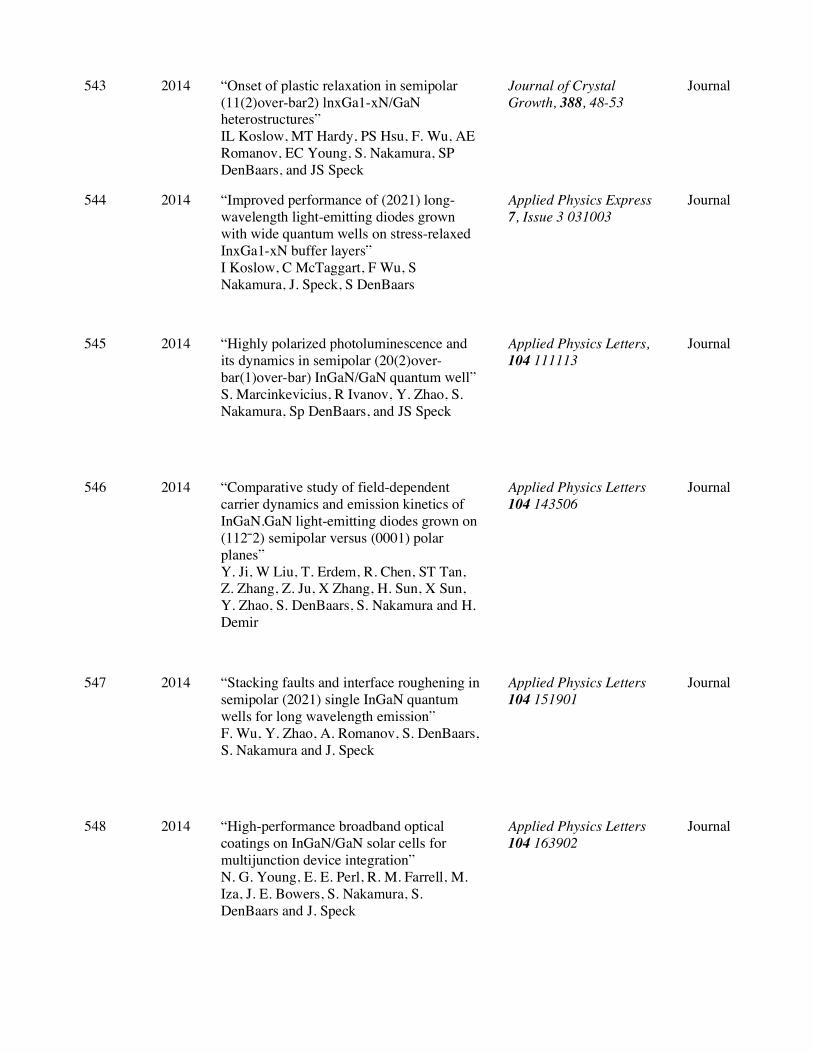
543 2014 “Onset of plastic relaxation in semipolar (11(2)over-bar2) lnxGa1-xN/GaN heterostructures” IL Koslow, MT Hardy, PS Hsu, F. Wu, AE Romanov, EC Young, S. Nakamura, SP DenBaars, and JS Speck
Journal of Crystal Growth, 388, 48-53
Journal
544 2014 “Improved performance of (2021) long-wavelength light-emitting diodes grown with wide quantum wells on stress-relaxed InxGa1-xN buffer layers” I Koslow, C McTaggart, F Wu, S Nakamura, J. Speck, S DenBaars
Applied Physics Express 7, Issue 3 031003
Journal
545 2014 “Highly polarized photoluminescence and its dynamics in semipolar (20(2)over-bar(1)over-bar) InGaN/GaN quantum well” S. Marcinkevicius, R Ivanov, Y. Zhao, S. Nakamura, Sp DenBaars, and JS Speck
Applied Physics Letters, 104 111113
Journal
546 2014 “Comparative study of field-dependent carrier dynamics and emission kinetics of InGaN.GaN light-emitting diodes grown on (112¯2) semipolar versus (0001) polar planes” Y. Ji, W Liu, T. Erdem, R. Chen, ST Tan, Z. Zhang, Z. Ju, X Zhang, H. Sun, X Sun, Y. Zhao, S. DenBaars, S. Nakamura and H. Demir
Applied Physics Letters 104 143506
Journal
547 2014 “Stacking faults and interface roughening in semipolar (2021) single InGaN quantum wells for long wavelength emission” F. Wu, Y. Zhao, A. Romanov, S. DenBaars, S. Nakamura and J. Speck
Applied Physics Letters 104 151901
Journal
548 2014 “High-performance broadband optical coatings on InGaN/GaN solar cells for multijunction device integration” N. G. Young, E. E. Perl, R. M. Farrell, M. Iza, J. E. Bowers, S. Nakamura, S. DenBaars and J. Speck
Applied Physics Letters 104 163902
Journal
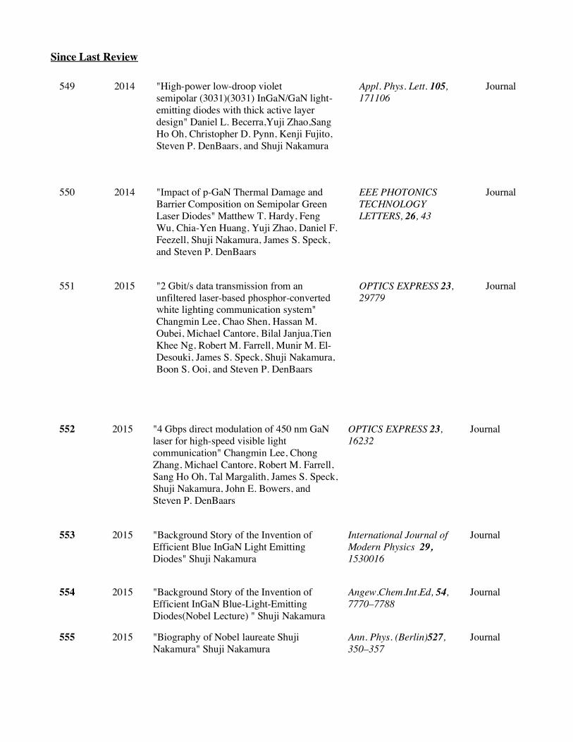
Since Last Review
549 2014 "High-power low-droop violet semipolar (3031)(3031) InGaN/GaN light-emitting diodes with thick active layer design" Daniel L. Becerra,Yuji Zhao,Sang Ho Oh, Christopher D. Pynn, Kenji Fujito, Steven P. DenBaars, and Shuji Nakamura
Appl. Phys. Lett. 105, 171106
Journal
550 2014 "Impact of p-GaN Thermal Damage and Barrier Composition on Semipolar Green Laser Diodes" Matthew T. Hardy, Feng Wu, Chia-Yen Huang, Yuji Zhao, Daniel F. Feezell, Shuji Nakamura, James S. Speck, and Steven P. DenBaars
EEE PHOTONICS TECHNOLOGY LETTERS, 26, 43
Journal
551 2015 "2 Gbit/s data transmission from an unfiltered laser-based phosphor-converted white lighting communication system" Changmin Lee, Chao Shen, Hassan M. Oubei, Michael Cantore, Bilal Janjua,Tien Khee Ng, Robert M. Farrell, Munir M. El-Desouki, James S. Speck, Shuji Nakamura, Boon S. Ooi, and Steven P. DenBaars
OPTICS EXPRESS 23, 29779
Journal
552 2015 "4 Gbps direct modulation of 450 nm GaN
laser for high-speed visible light communication" Changmin Lee, Chong Zhang, Michael Cantore, Robert M. Farrell, Sang Ho Oh, Tal Margalith, James S. Speck, Shuji Nakamura, John E. Bowers, and Steven P. DenBaars
OPTICS EXPRESS 23, 16232
Journal
553 2015 "Background Story of the Invention of Efficient Blue InGaN Light Emitting Diodes" Shuji Nakamura
International Journal of Modern Physics 29, 1530016
Journal
554 2015 "Background Story of the Invention of Efficient InGaN Blue-Light-Emitting Diodes(Nobel Lecture) " Shuji Nakamura
Angew.Chem.Int.Ed, 54, 7770–7788
Journal
555 2015 "Biography of Nobel laureate Shuji Nakamura" Shuji Nakamura
Ann. Phys. (Berlin)527, 350–357
Journal
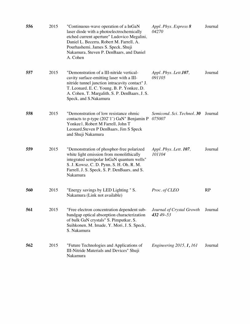
556 2015 "Continuous-wave operation of a InGaN laser diode with a photoelectrochemically etched current aperture" Ludovico Megalini, Daniel L. Becerra, Robert M. Farrell, A. Pourhashemi, James S. Speck, Shuji Nakamura, Steven P. DenBaars, and Daniel A. Cohen
Appl. Phys. Express 8 04270
Journal
557 2015 "Demonstration of a III-nitride vertical-cavity surface-emitting laser with a III-nitride tunnel junction intracavity contact" J. T. Leonard, E. C. Young, B. P. Yonkee, D. A. Cohen, T. Margalith, S. P. DenBaars, J. S. Speck, and S.Nakamura
Appl. Phys. Lett.107, 091105
Journal
558 2015 "Demonstration of low resistance ohmic contacts to p-type (202̄1̄) GaN" Benjamin P Yonkee1, Robert M Farrell, John T Leonard,Steven P DenBaars, Jim S Speck and Shuji Nakamura
Semicond. Sci. Technol. 30 075007
Journal
559 2015 "Demonstration of phosphor-free polarized white light emission from monolithically integrated semipolar InGaN quantum wells" S. J. Kowsz, C. D. Pynn, S. H. Oh, R. M. Farrell, J. S. Speck, S. P. DenBaars, and S. Nakamura
Appl. Phys. Lett. 107, 101104
Journal
560 2015 "Energy savings by LED Lighting " S. Nakamura (Link not available)
Proc. of CLEO RP
561 2015 "Free electron concentration dependent sub-bandgap optical absorption characterization of bulk GaN crystals" S. Pimputkar, S. Suihkonen, M. Imade, Y. Mori, J. S. Speck, S. Nakamura
Journal of Crystal Growth 432 49–53
Journal
562 2015 "Future Technologies and Applications of III-Nitride Materials and Devices" Shuji Nakamura
Engineering 2015, 1, 161 Journal

563 2015 "High optical power and low-efficiency droop blue light-emitting diodes using compositionally step-graded InGaN barrier" Chih-Chien Pan, Qimin Yan, Houqiang Fu, Yuji Zhao, Yuh-Renn Wu, Chris Van de Walle, Shuji Nakamura and Steven P. DenBaars
ELECTRONICS LETTERS 51 1187–1189
Journal
564 2015 "High spatial uniformity of photoluminescence spectra in semipolar plane (2021) InGaN/GaN quantum wells" K. Gelžinytė, R. Ivanov, S. Marcinkevičius, Y. Zhao, D. L. Becerra, S. Nakamura, S. P. DenBaars, and J. S. Speck
Journal of Applied Physics 117, 023111
Journal
565 2015 "High-power blue laser diodes with indium tin oxide cladding on semipolar (2021) GaN substrates" A. Pourhashemi, R. M.Farrell, A.Cohen, S. Speck, P. DenBaars and S. Nakamura
Appl. Phys. Lett. 106, 111105
Journal
566 2015 "Impact of carrier localization on radiative recombination times in semipolar (2021) plane InGaN/GaN quantum wells" R. Ivanov, S. Marcinkevičius, Y. Zhao, D. L. Becerra, S. Nakamura, S. P. DenBaars, and J. S. Speck
Appl. Phys. Lett. 107, 211109
Journal
567 2015 "InGaN lattice constant engineering via growth on(In,Ga)N/GaN nanostripe arrays" Stacia Keller, Cory Lund, Tyler Whyland, Yanling Hu, Carl Neufeld, Silvia Chan, Steven Wienecke, Feng Wu, Shuji Nakamura, James S Speck, Steven P DenBaars and Umesh K Mishra
Semicond. Sci. Technol. 30 105020
Journal
568 2015 "Low damage dry etch for III-nitride light emitters" Joseph G Nedy, Nathan G Young, Kathryn M Kelchner, Yanling Hu, Robert M Farrell, Shuji Nakamura, Steven P DenBaars, Claude Weisbuch and James S Speck
2015 Semicond. Sci. Technol. 30 085019
Journal
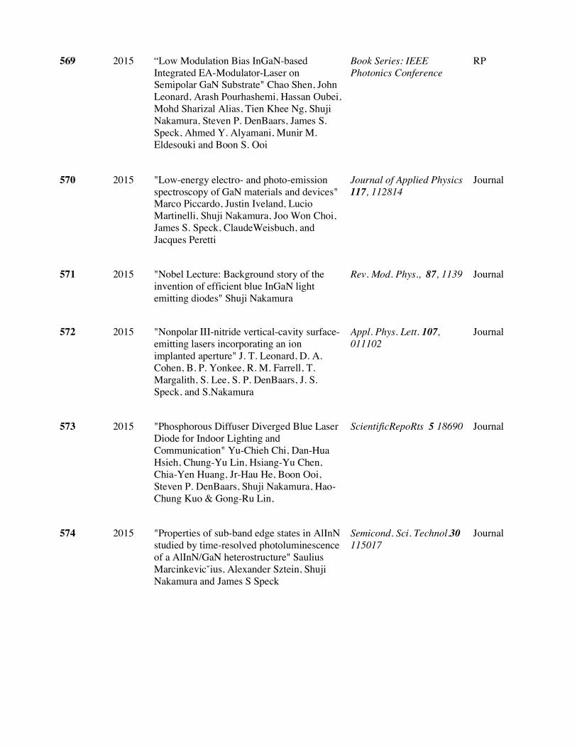
569 2015 “Low Modulation Bias InGaN-based Integrated EA-Modulator-Laser on Semipolar GaN Substrate" Chao Shen, John Leonard, Arash Pourhashemi, Hassan Oubei, Mohd Sharizal Alias, Tien Khee Ng, Shuji Nakamura, Steven P. DenBaars, James S. Speck, Ahmed Y. Alyamani, Munir M. Eldesouki and Boon S. Ooi
Book Series: IEEE Photonics Conference
RP
570 2015 "Low-energy electro- and photo-emission spectroscopy of GaN materials and devices" Marco Piccardo, Justin Iveland, Lucio Martinelli, Shuji Nakamura, Joo Won Choi, James S. Speck, ClaudeWeisbuch, and Jacques Peretti
Journal of Applied Physics 117, 112814
Journal
571 2015 "Nobel Lecture: Background story of the invention of efficient blue InGaN light emitting diodes" Shuji Nakamura
Rev. Mod. Phys., 87, 1139 Journal
572 2015 "Nonpolar III-nitride vertical-cavity surface-emitting lasers incorporating an ion implanted aperture" J. T. Leonard, D. A. Cohen, B. P. Yonkee, R. M. Farrell, T. Margalith, S. Lee, S. P. DenBaars, J. S. Speck, and S.Nakamura
Appl. Phys. Lett. 107, 011102
Journal
573 2015 "Phosphorous Diffuser Diverged Blue Laser Diode for Indoor Lighting and Communication" Yu-Chieh Chi, Dan-Hua Hsieh, Chung-Yu Lin, Hsiang-Yu Chen, Chia-Yen Huang, Jr-Hau He, Boon Ooi, Steven P. DenBaars, Shuji Nakamura, Hao-Chung Kuo & Gong-Ru Lin,
ScientificRepoRts 5 18690 Journal
574 2015 "Properties of sub-band edge states in AlInN studied by time-resolved photoluminescence of a AlInN/GaN heterostructure" Saulius Marcinkevicˇius, Alexander Sztein, Shuji Nakamura and James S Speck
Semicond. Sci. Technol.30 115017
Journal

575 2015 "Selective and controllable lateral photoelectrochemical etching of nonpolar and semipolar InGaN/GaN multiple quantum well active regions" Ludovico Megalini, Leah Y. Kuritzky, John T. Leonard, Renuka Shenoy, Kenneth Rose, Shuji Nakamura, James S. Speck, Daniel A. Cohen, and Steven P. DenBaars
Appl. Phys. Express 8 066502
Journal
576 2015 "Smooth e-beam-deposited tin-doped indium oxide for III-nitride vertical-cavity surface-emitting laser intracavity contacts" J. T. Leonard, D. A. Cohen, B. P. Yonkee, R. M. Farrell, S. P. DenBaars, J. S. Speck, and S. Nakamura
Journal of Applied Physics 118, 145304
Journal
577 2015 "Spatial variations of optical properties of semipolar InGaN quantum wells" Saulius Marcinkevičius, Kristina Gelžinytė, Ruslan Ivanov, Yuji Zhao, Shuji Nakamura, Steven P. DenBaars, James S. Speck
Proc. of SPIE 9363 93631U-1
RP
578 2015 "Stable vicinal step orientations in m-plane GaN" K.M. Kelchner, L.Y. Kuritzky, S. Nakamura, S.P. DenBaars, J.S. Speck
Journal of Crystal Growth 411, 56
Journal
579 2015 "Thermally enhanced blue light-emitting diode" Jin Xue, Yuji Zhao, Sang-Ho Oh, William F. Herrington, James S. Speck, Steven P. DenBaars, Shuji Nakamura,and Rajeev J. Ram
Appl. Phys. Lett.107, 121109
Journal
580 2015 "Ultraviolet light emitting diodes by ammonia molecular beam epitaxy on metamorphic (2021) AlGaN/GaN buffer layers" E. C. Young, B.P. Yonkee, F. Wu, B.K. Saifaddin, D.A. Cohen, S. P. DenBaars, S. Nakamura, J.S. Speck
JOURNAL OF CRYSTAL GROWTH 425 , 389-392
Journal
581 2016 "A new system for sodiumflux growth of bulk GaN. Part I: System development" Paul Von Dollena, Siddha Pimputkar, Mohammed Abo Alreesh, Hamad Albrithen, Sami Suihkonen, Shuji Nakamura, James S. Speck
Journal of Crystal Growth 456 58
Journal

582 2016 "A new system for sodium flux growth of bulk GaN. Part II:in situ investigation of growth processes" Paul Von Dollen, Siddha Pimputkar, Mohammed Abo Alreesh, Shuji Nakamura, James S. Speck
Journal of Crystal Growth 456, 67
Journal
583 2016 "Acidic ammonothermal growth of gallium nitride in a liner-free molybdenum alloy autoclave" Thomas F. Malkowski, Siddha Pimputkar, James S. Speck, Steven P. DenBaars, Shuji Nakamura
Journal of Crystal Growth 456, 21
Journal
584 2016 "Application of UV-C LED activated PMS for the degradation of anatoxin-a" Shilpi Verma, Shuji Nakamura, Mika Sillanpää
Chemical Engineering Journal 284 122
Journal
585 2016 "Basic ammonothermal GaN growth in molybdenum capsules" S. Pimputkar, J. S. Speck, S. Nakamura
Journal of Crystal Growth 456 15
Journal
586 2016 "Chemically assisted ion beam etching of laser diode facets on nonpolar and semipolar orientations of GaN" L Y Kuritzky, D L Becerra, A Saud Abbas, J Nedy, S Nakamura,S P DenBaars and D A Cohen
Semicond. Sci. Technol.31 075008
Journal
587 2016 "Comparison of nonpolar III-nitride vertical-cavity surface-emitting lasers with tunnel junction and ITO intracavity contacts" J . T. Leonard, E. C. Young, B. P. Yonkee, D. A. Cohen, F. Shen,T. Margalith,T. K. Ng, S. P. DenBaars, B. S. Ooi, J. S. Speck, and S. Nakamura
Proc. of SPIE 9748, 97481B
RP
588 2016 "CW operation of high-power blue laser diodes with polished facets on semi-polar (2021) GaN substrates" A. Pourhashemi, R.M. Farrell, D.A. Cohen, D.L. Becerra, S.P. DenBaars and S. Nakamura
ELECTRONICS LETTERS 52 2003-2004
Journal
589 2016 "Decomposition of supercritical ammonia and modeling of supercritical ammonia-nitrogen-hydrogen solutions with applicability towards ammonothermal conditions" Siddha Pimputkar Shuji Nakamura
The Journal of Supercritical Fluids 107, 17-30
Journal

590 2016 "Demonstration of a III-nitride edge-emitting laser diode utilizing a GaN tunnel junction contact" Benjamin P. Yonkee, Erin C. Young, Changmin Lee, John T. Leonard, Steven P. DenBaars, James S. Speck, and Shuji Nakamura
OPTICS EXPRESS 24, 7816
Journal
591 2016 "Designing optically pumped InGaN quantum wells with long wavelength emission for a phosphor-free device with polarized white light emission" Stacy J. Kowsz; Christopher D. Pynn; Feng Wu; Robert M. Farrell; James S. Speck; Steven P. DenBaars; Shuji Nakamura
Proc. of SPIE 9748 RP
592 2016 "Development of c-Plane Thin-Film Flip-Chip LEDs Fabricated by Photo-electrochemical (PEC) Liftoff" D. Hwang, B. Yonkee, R. M. Farrell, S. Nakamura, J. S. Speck and S. P. DenBaars
Proc. of IPRM/ISCS RP
593 2016 "Dynamic characteristics of 410 nm semipolar III-nitride laser diodes with a modulation bandwidth of over 5 GHz" Changmin Lee, Chong Zhang, Daniel L. Becerra, Seunggeun Lee, Charles A. Forman, Sang Ho Oh, Robert M. Farrell, James S. Speck, Shuji Nakamura, John E. Bowers, and Steven P. DenBaars
Appl. Phys. Lett. 109, 101104
Journal
594 2016 "Effects of active region design on gain and carrier injection and transport of CW semipolar InGaN laser diodes" Daniel L. Becerra, Daniel A. Cohen, Robert M. Farrell, Steven P. DenBaars, and Shuji Nakamura
Appl. Phys. Express 9 092104
Journal
595 2016 "Enhancing Light Extraction from III-Nitride Devices Using Moth-Eye Nanostructures Formed by Colloidal Lithography" Christopher D. Pynn, Federico L. Gonzalez, Lesley Chan, Alexander Berry, Sang Ho Oh, Tal Margalith, Daniel E. Morse, Shuji Nakamura, Michael J. Gordon, Steven P. DenBaars (Link not available)
Proc. of IPRM/ISCS RP

596 2016 "Estimation of roughness-induced scattering losses in III-nitride laser diodes with a photoelectrochemically etched current aperture" Ludovico Megalini, Renuka Shenoy, Kenneth Rose, James P. Speck, John E. Bowers,Shuji Nakamura, Daniel A. Cohen, and Steven P. DenBaars
Phys. Status Solidi A213, 953–957
Journal
597 2016 "Flip-chip blue LEDs grown on (2021) bulk GaN substrates utilizing photoelectrochemical etching for substrate removal" Benjamin P. Yonkee, Burhan SaifAddin, John T. Leonard, Steven P. DenBaars, and Shuji Nakamura
Appl. Phys. Express 9056502
Journal
598 2016 "Germanium doping of GaN by metalorganic chemical vapor deposition for polarization screening applications" N.G. Young, R.M. Farrell, M. Iza, S. Nakamura, S.P. DenBaars, C. Weisbuch, J.S. Speck
Journal of Crystal Growth 455 105–110
Journal
599 2016 "GHz modulation bandwidth from single-longitudinal mode violet-blue VCSEL using nonpolar InGaN/GaN QWs" Shen, Chao; Leonard, John T.; Young, Erin C.; et al.
Proc. of CLEO RP
600 2016 "GHz Modulation Enabled Using Large Extinction Ratio Waveguide-Modulator Integrated with InGaN Laser Diode" Chao Shen,Changmin Lee,Tien Khee Ng, James S. Speck, Shuji Nakamura, Steven P. DenBaars, Ahmed Y. Alyamani, Munir M. Eldesouki and Boon S. Ooi
Japanese Journal of Applied Physics, 57, 08PA06
Journal
601 2016 "Green semipolar III-nitride light-emitting diodes grown by limited area epitaxy" C. D. Pynn, S. J. Kowsz, S. H. Oh, H. Gardner, R. M. Farrell, S. Nakamura, J. S. Speck, and S. P. DenBaars
Appl. Phys. Lett.109, 041107
Journal
602 2016 "High Efficiency Semipolar III-Nitride Lasers for Solid State Lighting" D. L. Becerra, D. A. Cohen, R. M. Farrell, S. P. DenBaars and S. Nakamura
Proc. of ISLC RP
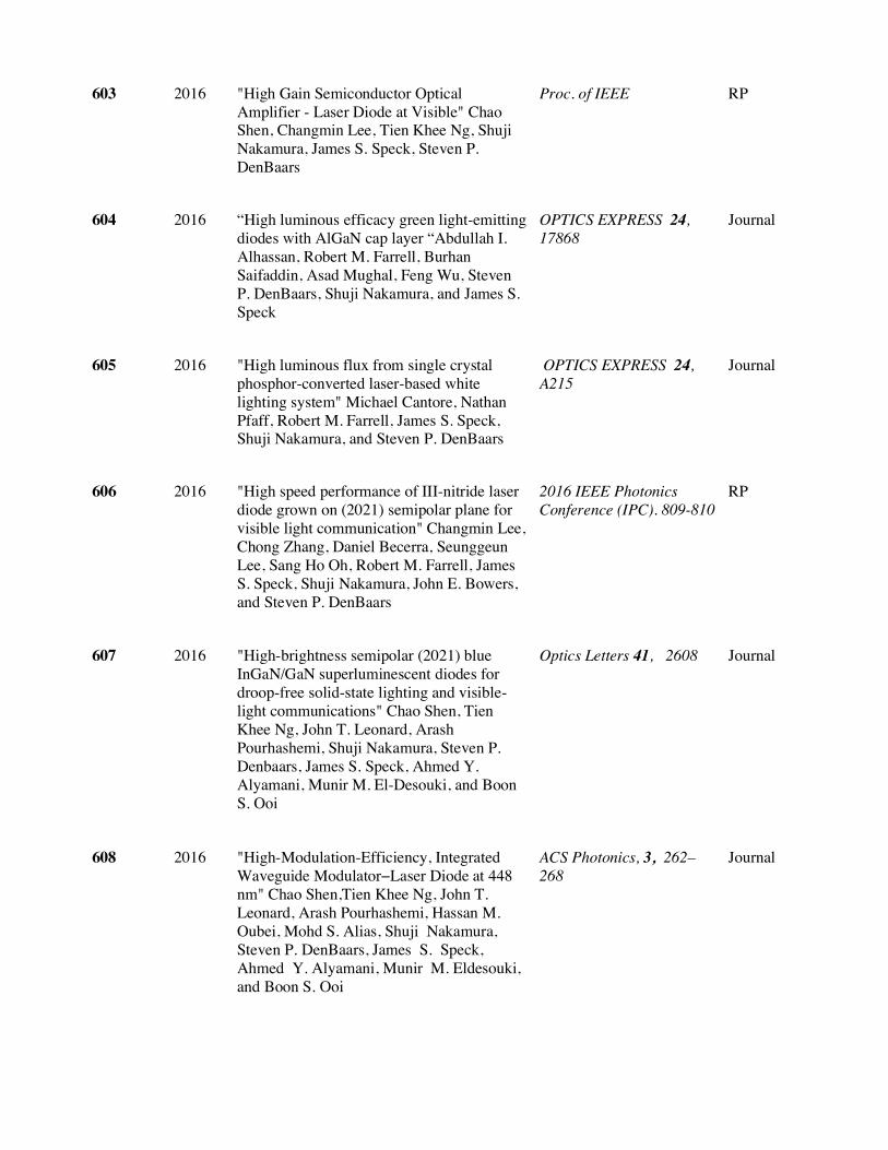
603 2016 "High Gain Semiconductor Optical Amplifier - Laser Diode at Visible" Chao Shen, Changmin Lee, Tien Khee Ng, Shuji Nakamura, James S. Speck, Steven P. DenBaars
Proc. of IEEE RP
604 2016 “High luminous efficacy green light-emitting diodes with AlGaN cap layer “Abdullah I. Alhassan, Robert M. Farrell, Burhan Saifaddin, Asad Mughal, Feng Wu, Steven P. DenBaars, Shuji Nakamura, and James S. Speck
OPTICS EXPRESS 24, 17868
Journal
605 2016 "High luminous flux from single crystal phosphor-converted laser-based white lighting system" Michael Cantore, Nathan Pfaff, Robert M. Farrell, James S. Speck, Shuji Nakamura, and Steven P. DenBaars
OPTICS EXPRESS 24, A215
Journal
606 2016 "High speed performance of III-nitride laser diode grown on (2021) semipolar plane for visible light communication" Changmin Lee, Chong Zhang, Daniel Becerra, Seunggeun Lee, Sang Ho Oh, Robert M. Farrell, James S. Speck, Shuji Nakamura, John E. Bowers, and Steven P. DenBaars
2016 IEEE Photonics Conference (IPC). 809-810
RP
607 2016 "High-brightness semipolar (2021) blue InGaN/GaN superluminescent diodes for droop-free solid-state lighting and visible-light communications" Chao Shen, Tien Khee Ng, John T. Leonard, Arash Pourhashemi, Shuji Nakamura, Steven P. Denbaars, James S. Speck, Ahmed Y. Alyamani, Munir M. El-Desouki, and Boon S. Ooi
Optics Letters 41, 2608 Journal
608 2016 "High-Modulation-Efficiency, Integrated Waveguide Modulator−Laser Diode at 448 nm" Chao Shen,Tien Khee Ng, John T. Leonard, Arash Pourhashemi, Hassan M. Oubei, Mohd S. Alias, Shuji Nakamura, Steven P. DenBaars, James S. Speck, Ahmed Y. Alyamani, Munir M. Eldesouki, and Boon S. Ooi
ACS Photonics, 3, 262–268
Journal

609 2016 "High-power LEDs using Ga-doped ZnO current-spreading layers" A.J. Mughal, S. Oh, A. Myzaferi, S. Nakamura, J.S. Speckand S.P. DenBaars
Electronics Letters 52, 304 – 306
Journal
610 2016 "High-speed 405-nm superluminescent diode (SLD) with 807-MHz modulation bandwidth" Chao Shen, Changmin Lee, Tien Khee Ng, Shuji Nakamura, James S. Speck, Steven P. Denbaars, Ahmed Y. Alyamani, Munir, M. El-Desouki, And Boon S. Ooi
OPTICS EXPRESS. 24, 20281
Journal
611 2016 "High-Speed Performance of III-nitride 410nm Ridge Laser Diode on plance for (202̲1) Visible Light Communication" Lee, Changmin; Zhang, Chong; Becerra, Daniel L.; et al.
Proc. of IPRM/ISCS RP
612 2016 "Hybrid MOCVD/MBE GaN Tunnel Junction LEDs with Greater than 70% Wall Plug Efficiency" Yonkee, Benjamin P.; Young, Erin C.; Leonard, John T.; et al.
Proc. of IPRM/ISCS RP
613 2016 "Hybrid tunnel junction contacts to III–nitride light-emitting diodes" Erin C. Young, Benjamin P. Yonkee, Feng Wu, Sang Ho Oh, Steven P. DenBaars, Shuji Nakamura, and James S. Speck
Appl. Phys. Express 9 022102
Journal
614 2016 "Incorporation and effects of impurities in different growth zones within basic ammonothermal GaN" Sakari Sintonena, Pyry Kivisaari, Siddha Pimputkar, Sami Suihkonen, Tobias Schulz, James S. Speck, Shuji Nakamura
Journal of Crystal Growth 456, 43-50
Journal
615 2016 "Infrared absorption of hydrogen-related defects in ammonothermal GaN" Suihkonen, Sami; Pimputkar, Siddha; Speck, James S.; Nakamura, Shuji
APPLIED PHYSICS LETTERS 108(20),
Journal
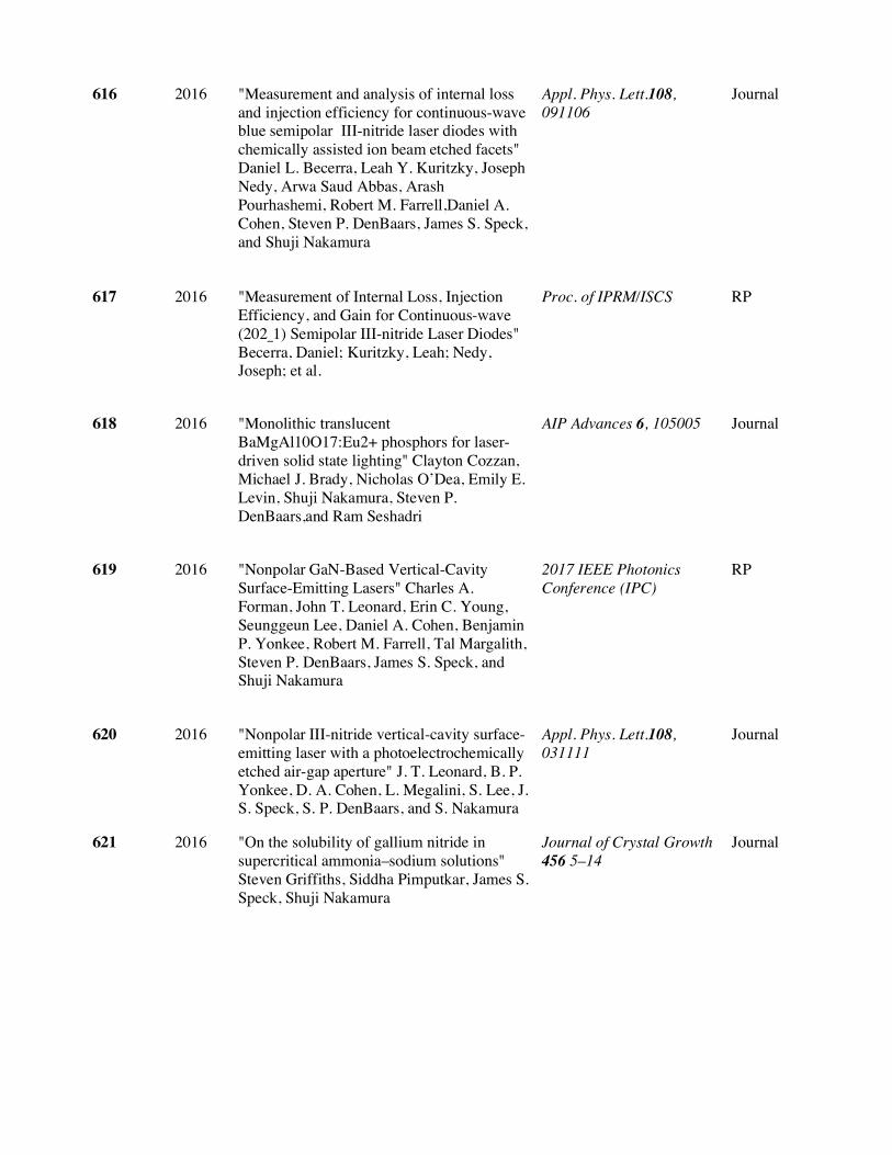
616 2016 "Measurement and analysis of internal loss and injection efficiency for continuous-wave blue semipolar III-nitride laser diodes with chemically assisted ion beam etched facets" Daniel L. Becerra, Leah Y. Kuritzky, Joseph Nedy, Arwa Saud Abbas, Arash Pourhashemi, Robert M. Farrell,Daniel A. Cohen, Steven P. DenBaars, James S. Speck, and Shuji Nakamura
Appl. Phys. Lett.108, 091106
Journal
617 2016 "Measurement of Internal Loss, Injection Efficiency, and Gain for Continuous-wave (202̲1) Semipolar III-nitride Laser Diodes" Becerra, Daniel; Kuritzky, Leah; Nedy, Joseph; et al.
Proc. of IPRM/ISCS RP
618 2016 "Monolithic translucent BaMgAl10O17:Eu2+ phosphors for laser-driven solid state lighting" Clayton Cozzan, Michael J. Brady, Nicholas O’Dea, Emily E. Levin, Shuji Nakamura, Steven P. DenBaars,and Ram Seshadri
AIP Advances 6, 105005 Journal
619 2016 "Nonpolar GaN-Based Vertical-Cavity Surface-Emitting Lasers" Charles A. Forman, John T. Leonard, Erin C. Young, Seunggeun Lee, Daniel A. Cohen, Benjamin P. Yonkee, Robert M. Farrell, Tal Margalith, Steven P. DenBaars, James S. Speck, and Shuji Nakamura
2017 IEEE Photonics Conference (IPC)
RP
620 2016 "Nonpolar III-nitride vertical-cavity surface-emitting laser with a photoelectrochemically etched air-gap aperture" J. T. Leonard, B. P. Yonkee, D. A. Cohen, L. Megalini, S. Lee, J. S. Speck, S. P. DenBaars, and S. Nakamura
Appl. Phys. Lett.108, 031111
Journal
621 2016 "On the solubility of gallium nitride in supercritical ammonia–sodium solutions" Steven Griffiths, Siddha Pimputkar, James S. Speck, Shuji Nakamura
Journal of Crystal Growth 456 5–14
Journal
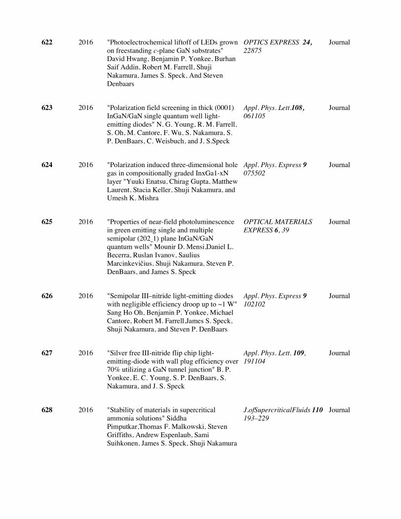
622 2016 "Photoelectrochemical liftoff of LEDs grown on freestanding c-plane GaN substrates" David Hwang, Benjamin P. Yonkee, Burhan Saif Addin, Robert M. Farrell, Shuji Nakamura, James S. Speck, And Steven Denbaars
OPTICS EXPRESS 24, 22875
Journal
623 2016 "Polarization field screening in thick (0001) InGaN/GaN single quantum well light-emitting diodes" N. G. Young, R. M. Farrell, S. Oh, M. Cantore, F. Wu, S. Nakamura, S. P. DenBaars, C. Weisbuch, and J. S.Speck
Appl. Phys. Lett.108, 061105
Journal
624 2016 "Polarization induced three-dimensional hole gas in compositionally graded InxGa1-xN layer "Yuuki Enatsu, Chirag Gupta, Matthew Laurent, Stacia Keller, Shuji Nakamura, and Umesh K. Mishra
Appl. Phys. Express 9 075502
Journal
625 2016 "Properties of near-field photoluminescence in green emitting single and multiple semipolar (202̲1) plane InGaN/GaN quantum wells" Mounir D. Mensi,Daniel L. Becerra, Ruslan Ivanov, Saulius Marcinkevičius, Shuji Nakamura, Steven P. DenBaars, and James S. Speck
OPTICAL MATERIALS EXPRESS 6, 39
Journal
626 2016 "Semipolar III–nitride light-emitting diodes with negligible efficiency droop up to ~1 W" Sang Ho Oh, Benjamin P. Yonkee, Michael Cantore, Robert M. Farrell,James S. Speck, Shuji Nakamura, and Steven P. DenBaars
Appl. Phys. Express 9 102102
Journal
627 2016 "Silver free III-nitride flip chip light-emitting-diode with wall plug efficiency over 70% utilizing a GaN tunnel junction" B. P. Yonkee, E. C. Young, S. P. DenBaars, S. Nakamura, and J. S. Speck
Appl. Phys. Lett. 109, 191104
Journal
628 2016 "Stability of materials in supercritical ammonia solutions" Siddha Pimputkar,Thomas F. Malkowski, Steven Griffiths, Andrew Espenlaub, Sami Suihkonen, James S. Speck, Shuji Nakamura
J.ofSupercriticalFluids 110 193–229
Journal

629 2016 "Study of Low-Efficiency Droop in Semipolar (2021)InGaN Light-Emitting Diodes by Time-Resolved Photoluminescence" Houqiang Fu, Zhijian Lu, Xin-Hao Zhao, Yong-Hang Zhang, Fellow, IEEE, Steven P. DenBaars, Fellow, IEEE,Shuji Nakamura, and Yuji Zhao
JOURNAL OF DISPLAY TECHNOLOGY, 12, 736
Journal
630 2016 "Tunnel junction devices with monolithic optically pumped and electrically injected InGaN quantum wells for polarized white light emission" Kowsz, Stacy; Pynn, Christopher; Farrell, Robert; et al
Proc. of IPRM/ISCS RP
631 2016 "Using band engineering to tailor the emission spectra of trichromatic semipolar InGaN light-emitting diodes for phosphor-free polarized white light emission" S. J. Kowsz, C. D. Pynn, S. H. Oh, R. M. Farrell, S. P. DenBaars, and S. Nakamura
Journal of Applied Physics 120, 033102
Journal
632 2017 "Blue Laser Diode Based Free-space Optical Data Transmission elevated to 18Gbps over 16m" Yu-Fang Huang, Yu-Chieh Chi, Hsuan-Yun Kao, Chen-Ting Tsai, Huai-Yung Wang, Hao-Chung Kuo, Shuji Nakamura, Ding-Wei Huang & Gong-Ru Lin
ScientificRepoRts 7: 10478 Journal
633 2017 "Digital growth of thick N-polar InGaN films on relaxed InGaN pseudosubstrates" Cory Lund, Karine Hestroffer, Nirupam Hatui, Shuji Nakamura,Steven P. DenBaars, Umesh K. Mishra, and Stacia Keller
Appl. Phys. Express 10 111001
Journal
634 2017 "Efficient Semipolar (11−22) 550 nm Yellow/Green InGaN Light-Emitting Diodes on Low Defect Density (11−22) GaN/SapphireTemplates" Hongjian Li,Michel Khoury,Bastien Bonef, Abdullah I. Alhassan, Asad J. Mughal, Ezzah Azimah, Muhammad E.A. Samsudin, Philippe De Mierry, Shuji Nakamura, James S. Speck, and Steven P. DenBaars
ACS Appl. Mater. Interfaces 2017, 9, 36417-36422
Journal
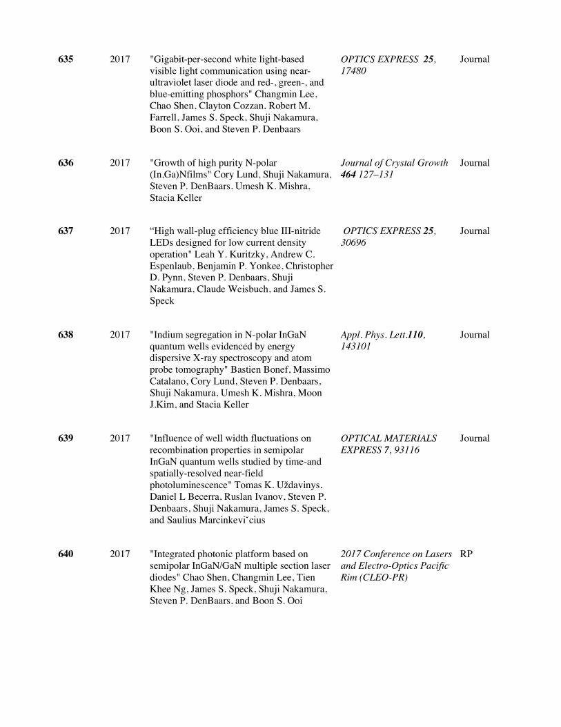
635 2017 "Gigabit-per-second white light-based visible light communication using near-ultraviolet laser diode and red-, green-, and blue-emitting phosphors" Changmin Lee, Chao Shen, Clayton Cozzan, Robert M. Farrell, James S. Speck, Shuji Nakamura, Boon S. Ooi, and Steven P. Denbaars
OPTICS EXPRESS 25, 17480
Journal
636 2017 "Growth of high purity N-polar (In,Ga)Nfilms" Cory Lund, Shuji Nakamura, Steven P. DenBaars, Umesh K. Mishra, Stacia Keller
Journal of Crystal Growth 464 127–131
Journal
637 2017 “High wall-plug efficiency blue III-nitride LEDs designed for low current density operation" Leah Y. Kuritzky, Andrew C. Espenlaub, Benjamin P. Yonkee, Christopher D. Pynn, Steven P. Denbaars, Shuji Nakamura, Claude Weisbuch, and James S. Speck
OPTICS EXPRESS 25, 30696
Journal
638 2017 "Indium segregation in N-polar InGaN quantum wells evidenced by energy dispersive X-ray spectroscopy and atom probe tomography" Bastien Bonef, Massimo Catalano, Cory Lund, Steven P. Denbaars, Shuji Nakamura, Umesh K. Mishra, Moon J.Kim, and Stacia Keller
Appl. Phys. Lett.110, 143101
Journal
639 2017 "Influence of well width fluctuations on recombination properties in semipolar InGaN quantum wells studied by time-and spatially-resolved near-field photoluminescence" Tomas K. Uždavinys, Daniel L Becerra, Ruslan Ivanov, Steven P. Denbaars, Shuji Nakamura, James S. Speck, and Saulius Marcinkeviˇcius
OPTICAL MATERIALS EXPRESS 7, 93116
Journal
640 2017 "Integrated photonic platform based on semipolar InGaN/GaN multiple section laser diodes" Chao Shen, Changmin Lee, Tien Khee Ng, James S. Speck, Shuji Nakamura, Steven P. DenBaars, and Boon S. Ooi
2017 Conference on Lasers and Electro-Optics Pacific Rim (CLEO-PR)
RP

641 2017 “Metal-organic chemical vapor deposition of high quality, high indium composition N-polar InGaN layers for tunnel devices" Cory Lund, Brian Romanczyk, Massimo Catalano, Qingxiao Wang, Wenjun Li, Domenic DiGiovanni, Moon J.Kim, Patrick Fay, Shuji Nakamura, Steven P. DenBaars, Umesh K. Mishra, and StaciaKeller
Journal of Applied Physics 121, 185707
Journal
642 2017 "Nonpolar and semipolar InGaN/GaN multiple-quantum-well solar cells with improved carrier collection efficiency" Xuanqi Huang, Houqiang Fu, Hong Chen, Xiaodong Zhang, Zhijian Lu, Jossue Montes, Michael Iza, Steven P.DenBaars, Shuji Nakamura, and Yuji Zhao
Appl. Phys. Lett. 110, 161105
Journal
643 2017 "Nonpolar GaN-Based Vertical-Cavity Surface-Emitting Lasers" Forman, Charles A.; Lee, SeungGeun; Young, Erin C.; et al.
Proc. of IEEE-Photonics-Societ, 233-234
RP
644 2017 "Optoelectronic properties of doped hydrothermal ZnO thin films" Asad J. Mughal, Benjamin Carberry, Sang Ho Oh, Anisa Myzaferi, James S. Speck, Shuji Nakamura,and Steven P. DenBaars
Phys. Status Solidi A214, 1600941
Journal
645 2017 "P–n junction diodes with polarization induced p-type graded InxGa1–xN layer" Yuuki Enatsu, Chirag Gupta, Stacia Keller, Shuji Nakamura and Umesh K Mishra
Semicond. Sci. Technol. 32 105013
Journal
646 2017 "Polarization-enhanced InGaN/GaN-based hybrid tunnel junction contacts to GaN p–n diodes andInGaN LEDs" Asad J. Mughal, Erin C. Young, Abdullah I. Alhassan, Joonho Back, Shuji Nakamura, James S. Speck, and Steven P. DenBaars
Appl. Phys. Express 10 121006
Journal
647 2017 "Polarization-Resolved Near-Field Spectroscopy of Localized States in m-Plane InxGa1-xN/GaN Quantum Wells" Ruslan Ivanov,Saulius Marcinkevičius, Mounir D. Mensi, Oscar Martinez, Leah Y. Kuritzky, Daniel J. Myers,Shuji Nakamura, and James S. Speck
PHYSICAL REVIEW APPLIED 7,064033
Journal

648 2017 "Scanning near-field microscopy of carrier lifetimes in m-plane InGaN quantum wells" Ruslan Ivanov, Saulius Marcinkevičius, Tomas K. Uždavinys, Leah Y. Kuritzky, Shuji Nakamura, and James S.Speck
Appl. Phys. Lett.110, 031109
Journal
649 2017 "Semipolar (202¯1) III-Nitride P-Down LEDs with in situ anneal to reduce the Mg memory effect" C. Forman, J. Leonard, B. Yonkee, C. Pynn, T. Mates, D. Cohen, R. Farrell, T. Margalith,S. DenBaars, J. Speck, S. Nakamura
Journal of Crystal Growth 464 197–200
Journal
650 2017 "Semipolar III-nitride laser diodes with zinc oxide cladding"Anisa Myzaferi, Arthur H.Reading, Robert M.Farrell, Daniel A.Cohen, Shuji Nakamura, and Steven P.Denbaars
OPTICS EXPRESS 25 16922
Journal
651 2017 "Semipolar III–nitride quantum well waveguidephotodetector integrated with laser diode for on-chip photonic system" Chao Shen, Changmin Lee, Edgars Stegenburgs, Jorge Holguin Lerma, Tien Khee Ng, Shuji Nakamura,Steven P. DenBaars, Ahmed Y. Alyamani, Munir M. El-Desouki, and Boon S. Ooi
Appl. Phys. Express 10 042201
Journal
652 2017 "Semipolar InGaN-based superluminescent diodes for solid-state lighting and visible lightcommunications" Chao Shen, Tien Khee Ng, Changmin Lee, John T. Leonard, Shuji Nakamura, et al.
Proc. SPIE10104, Gallium Nitride Materials and Devices XII, 101041U
RP
653 2017 "Smooth and selective photo-electrochemical etching of heavily doped GaN:Si using a mode-locked 355 nm microchip laser" Seung Geun Lee, Saadat Mishkat-Ul-Masabih, John T. Leonard, Daniel F. Feezell, Daniel A. Cohen, James S. Speck, Shuji Nakamura, and Steven P. DenBaars
Appl. Phys. Express 10 011001
Journal

654 2017 "Structural and Optical Properties of Group III Doped Hydrothermal ZnO Thin Films" Asad J. Mughal, Benjamin Carberry, James S. Speck, Shuji Nakamura, and Steven P. Denbaars
Journal of ELECTRONIC MATERIALS, 46, 1821
Journal
655 2017 "Sustained high external quantum efficiency in ultrasmall blue III–nitride micro-LEDs" David Hwang, Asad Mughal, Christopher D. Pynn, Shuji Nakamura, and Steven P. DenBaars
Appl. Phys. Express 10 032101
Journal
656 2017 "Techniques to reduce thermal resistance in flip-chip GaN-based VCSELs" Saadat Mishkat-Ul-Masabih, John Leonard, Daniel Cohen, Shuji Nakamura, and Daniel Feezell
Phys. Status Solidi A214, 8, 1600819
Journal
657 2017 "Toward ultimate efficiency:progress and prospects on planar and 3D nanostructurednonpolar and semipolar InGaN light-emitting diodes" Yuji Zhao, Houqiang Fu, George T. Wang, and Shuji Nakamura
Advances in Optics and Photonics 10, 246
Journal
658 2017 "Using tunnel junctions to grow monolithically integrated optically pumped semipolar III-nitride yellow quantum wells on top of electrically injected blue quantum wells" Stacy J. Kowsz, Erin C. Young, Benjamin P. Yonkee,Christopher D. Pynn, Robert M. Farrell, James S. Speck,Steven P. Denbaars,And Shuji Nakamura
OPTICS EXPRESS 25, 3841
Journal
659 2018 “An exploratory study of acidic ammonothermal growth in a TZM autoclave at high temperatures” Malkowski, Thomas F., Speck, James S., Denbaars, Steven P., Nakamura, Shuji
Journal of Crystal Growth 499, 85-89
Journal
660 2018 "Auger-generated hot carrier current in photo-excited forward biased single quantumwell blue light emitting diodes" Andrew C. Espenlaub, Abdullah I. Alhassan, Shuji Nakamura, Claude Weisbuch, and James S. Speck
Appl. Phys. Lett.112, 141106
Journal
661 2018 "Carrier dynamics of two distinct localized centers in 530 nm InGaN green light-emitting diodes" Panpan Li, Bastien Bonef, Michel Khoury, Guillaume Lheureux,Hongjian Li, Junjie Kang, Shuji Nakamura, Steven P. DenBaars,
Superlattices and Microstructures 113 684-689
Journal
662 2018 "Continuous-wave operation of m-plane GaN-based vertical-cavity surface-emitting lasers with a tunnel junction intracavity contact" Charles A. Forman, Seung Geun Lee, Erin C. Young, Jared A. Kearns, Daniel A. Cohen, John T. Leonard, Tal Margalith, Steven P. DenBaars, and Shuji Nakamura
Appl. Phys. Lett.112, 111106
Journal
663 2018 "Demonstration of enhanced continuous-wave operation of blue laser diodes on a semipolar 202̲1̲ GaN substrate using indium-tin-oxide/thin-p-GaN cladding layers" Shlomo Mehari, Daniel A.Cohen, Daniel L.Becerra, Shuji Nakamura, and Steven P. Denbaars
OPTICS EXPRESS 26, 1564
Journal
664 2018 "Development of high performance green c-plane III-nitride light-emitting diodes" Abdullah. I. Alhassan, Nathan. G. Young, Robert. M. Farrell, Christopher Pynn, Feng. Wu, Ahmed Y. Alyamani, Shuji Nakamura, Steven. P. Denbaars, and James. S. Speck
OPTICS EXPRESS 26, 5591
Journal
665 2018 “Digital processing with single electrons for arbitrary waveform generation of current” Okazaki, Yuma, Nakamura, Shuji, Onomitsu, Koji, Kaneko, Nobu-Hisa
Appl. Phys. Express 11, 3 Journal
666 2018 "Direct Measurement of Nanoscale Lateral Carrier Diffusion: Toward Scanning Diffusion Microscopy" Mounir Mensi, Ruslan Ivanov, Tomas K. Uždavinys, Kathryn M. Kelchner, Shuji Nakamura, Steven P. DenBaars, James S. Speck, and Saulius Marcinkevičius
ACS Photonics2018, 5, 528-534
Journal

667 2018 “Dynamical coupling between a nuclear spin ensemble and electromechanical phonons” Yuma Okazaki, Imran Mahboob, Koji Onomitsu, Satoshi Sasaki, Shuji Nakamura, Nobu-Hisa Kaneko & Hiroshi Yamaguchi
Nature Communications 9, 2993
Journal
668 2018 " Evidence of nanoscale Anderson localization induced by intrinsic compositional disorder in InGaN/GaN quantum wells by scanning tunneling luminescence spectroscopy" W. Hahn, M. Lentali, P. Polovodov, N. Young, S. Nakamura, J. S. Speck, C. Weisbuch, M. Filoche,Y.-R. Wu, M. Piccardo, F. Maroun, L. Martinelli, Y. Lassailly, and J. Peretti
PHYSICAL REVIEW B 98,045305
Journal
669 2018 “Fano effect in the transport of an artificial molecule” Shota Norimoto, Shuji Nakamura, Yuma Okazaki, Tomonori Arakawa, Kenichi Asano, Koji Onomitsu, Kensuke Kobayashi, and Nobu-hisa Kaneko
Pyshical Review B 97, 195313
Journal
670 2018 "GaN-based vertical-cavity surface-emitting lasers with tunnel junction contacts grown by metal-organic chemical vapor deposition" Seung Geun Lee, Charles A. Forman, Changmin Lee, Jared Kearns, Erin C. Young, John T. Leonard,Daniel A. Cohen, James S. Speck, Shuji Nakamura, and Steven P. DenBaars
Appl. Phys. Express 11 062703
Journal
671 2018 “High efficiency of III-nitride micro-light-emitting diodes by sidewall passivation using atomic layer deposition” Matthew S. Wong, David Hwang, Abdullah I. Alhassan, Changmin Lee, Ryan Ley, Shuji Nakamura, and Steven P. DenBaars
Optics Express 26, 16 Journal
672 2018 "High reflectivity Ohmic contacts to n-GaN utilizing vacuum annealed aluminum" Benjamin P. Yonkee, Erin C. Young, Steven P. DenBaars, James S. Speck and Shuji Nakamura
Semicond. Sci. Technol.33 015015
Journal
673 2018 "Invention, development, and status of the blue light-emitting diode, the enabler of solid-state lighting" Daniel Feezell, Shuji Nakamura
C.R.Physique 19 113–133 Journal
674 2018 “Investigation of Mg delta-doping for low resistance N-polar p-GaN films grown at reduced temperatures by MOCVD” Cory Lund, Anchal Agarwal, Brian Romanczyk, Thomas Mates, Shuji Nakamura, Steven P DenBaars, Umesh K Mishra and Stacia Keller
Semiconductor Science and Technology 33, 9
Journal
675 2018 "Low threading dislocation density aluminum nitride on silicon carbide through the use of reduced temperature interlayers" Humberto M. Foronda, Feng Wu, Christian Zollner, Muhammad Esmed Alif, Burhan Saifaddin, Abdullah Almogbel, Michael Iza, Shuji Nakamura, Steven P. DenBaars, James S. Speck
Journal of Crystal Growth 483 134–139
Journal
676 2018 "Metal-organic chemical vapor deposition of N-polar InN quantum dots and thin films on vicinal GaN" Cory Lund, Massimo Catalano, Luhua Wang, Christian Wurm, Thomas Mates, Moon Kim, Shuji Nakamura,Steven P. DenBaars, Umesh K. Mishra, and Stacia Keller
Journal of Applied Physics 123, 055702
Journal
677 2018 "Micro-light-emitting diodes with III–nitride tunnel junction contacts grown by metalorganic chemical vapor deposition" David Hwang, Asad J. Mughal, Matthew S. Wong, Abdullah I. Alhassan,Shuji Nakamura, and Steven P. DenBaars
Appl. Phys. Express 11 012102
Journal
678 2018 “Multimode scanning near-field photoluminescence spectroscopy of InGaN quantum wells” Marcinkevicius, Saulius, Mensi, Mounir, Ivanov, Ruslan, Kuritzky, Leah Y., DenBaars, Steven P., Nakamura, Shuji, Speck, James S.
2018 IEEE RESEARCH AND APPLICATIONS OF PHOTONICS IN DEFENSE CONFERENCE
Proceedings Paper
679 2018 "On the optical polarization properties of semipolar (2021) and (2021) InGaN/GaNquantum wells" Christian Mounir, Ingrid L. Koslow, Tim Wernicke, Michael Kneissl, Leah Y. Kuritzky, Nicholas L. Adamski, SangHo Oh, Christopher D. Pynn, Steven P. DenBaars, Shuji Nakamura, James S. Speck, and Ulrich T. Schwarz
Journal of Applied Physics 123, 085705
Journal
680 2018 “Optical Gain and Loss Measurements of Semipolar III-nitride Laser Diodes with ITO/thin-p-GaN Cladding Layers” Mehari, Shlomo, Cohen, Daniel A., Becerrea, Daniel L., Weisbuch, Claude, Nakamura, Shuji, DenBaars, Steven P.
2018 76TH DEVICE RESEARCH CONFERENCE (DRC)
Proceedings Paper
681 2018 "Reduced-droop green III–nitride light-emitting diodes utilizing GaN tunnel junction" Abdullah I. Alhassan, Erin C. Young, Ahmed Y. Alyamani, Abdulrahman Albadri, Shuji Nakamura, Steven P. DenBaars, and James S. Speck
Appl. Phys. Express11 042101
Journal
682 2018 "Semipolar (202̲1) GaN templates on sapphire: 432 nm InGaN light-emitting diodes and light extraction simulations" Michel Khoury, Hongjian Li, Bastien Bonef, Leah Y. Kuritzky, Asad J. Mughal,Shuji Nakamura, James S. Speck, and Steven P. DenBaars
Appl. Phys. Express11 036501
Journal
683 2018 “Semipolar GaN-based laser diodes for Gbit/s white lighting communication: devices to systems” Lee, Changmin; Shen, Chao; Farrell, Robert M.; Nakamura,Shuji; Ooi, Boon S.; Bowers, John E.; DenBaars, Steven P.; Speck, James S.; Cozzan, Clayton; Alyamani, Ahmed Y.
GALLIUM NITRIDE MATERIALS AND DEVICES XIII
Proceedings Paper
684 2018 "Semipolar InGaN quantum-well laser diode with integrated amplifier for visible light communications" Chao Shen, Tien Khee Ng, Changmin Lee, Shuji Nakamura, James S. Speck, Steven P. Denbaars, Ahmed Y. Alyamani, Munir M. El-Desouki, and Boon S. Ooi
OPTICS EXPRESS 26, A219
Journal

685 2018 " Stable, Heat-Conducting Phosphor Composites for High-Power Laser Lighting" Clayton Cozzan, Guillaume Lheureux, Nicholas O’Dea, Emily E. Levin, Jake Graser, Taylor D. Sparks, Shuji Nakamura, Steven P. DenBaars, Claude Weisbuch, and Ram Seshadri
ACS Appl. Mater. Interfaces2018, 10, 5673-5681
Journal
686 2018 “Toward ultimate efficiency: progress and prospects on planar and 3D nanostructured nonpolar and semipolar InGaN light-emitting diodes” Zhao, Yuji, Fu, Houqiang, Wang, George T., Nakamura, Shuji
ADVANCES IN OPTICS AND PHOTONICS
Review
687 2018 "Zinc oxide clad limited area epitaxy semipolar III-nitride laser diodes" Anisa Myzaferi, Asad J. Mughal, Daniel A. Cohen, Robert M. Farrell, Shuji Nakamura, James S. Speck, and Steven P. Denbaars
OPTICS EXPRESS 26, 12490
Journal
688 2019 “Compensation effects of high oxygen levels in semipolar AlGaN electron blocking layers and their mitigation via growth optimization” Becerra, Daniel L., Cohen, Daniel A., Mehari, Shlomo, DenBaars, Steven P., Nakamura, Shuji
Journal of Crystal Growth 507 118–123
Journal
690 2019 “Investigation of oxygen and other impurities and their effect on the transparency of a Na flux grown GaN crystal” Mohammed Abo Alreesh, Paul Von Dollen, Thomas F. Malkowskia, Tom Mates, Hamad Albrithen, Steven DenBaars, Shuji Nakamura, James S.Speck
Journal of Crystal Growth 508 50–57
Journal
691 2019 “Semipolar InGaN blue laser diodes with a low optical loss and a high material gain obtained by suppression of carrier accumulation in the p-waveguide region” Mehari, Shlomo, Cohen, Daniel A., Becerra, Daniel L., Nakamura, Shuji, DenBaars, Steven P.
Japanese Journal of Applied Physics 58, 2
Journal
692 2019 “Fabrication technology for high light- extraction ultraviolet thin-film flip-chip (UV TFFC) LEDs grown on SiC” SaifAddin, Burhan K.; Almogbel, Abdullah; Zollner, Christian J.; et al.
Semiconductor Science and Technology 34, 3
Journal

693 2019 "Enhancement of n-type GaN (20-21) semipolar surface morphology in photo-electrochemical undercut etching" Abbas, Arwa Saud; Alyamani, Ahmed Y.; Nakamura, Shuji; et al.
Appl. Phys. Express 12, 3 Journal
694 2019 “Efficient tunnel junction contacts for high-power semipolar III-nitride edge-emitting laser diodes” Hamdy, Kareem W.; Young, Erin C.; Alhassan, Abdullah, I; et al.
Optics Express 27, 6 Journal
695 2019 "Interwell carrier transport in InGaN/(In)GaN multiple quantum wells" Marcinkevicius, Saulius; Yapparov, Rinat; Kuritzky, Leah Y.; et al.
Applied Physics Letters 114, 15
Journal
696 2019 “Continuous-wave operation of a semipolar InGaN distributed-feedback blue laser diode with a first-order indium tin oxide surface grating” Zhang, Haojun; Cohen, Daniel A.; Chan, Philip; et al.
Optics Letters 44, 12 Journal
697 2019 “Infrared luminescence from N-polar InN quantum dots and thin films grown by metal organic chemical vapor deposition” Reilly, Caroline E.; Lund, Cory; Nakamura, Shuji; et al.
Applied Physics Letters 114, 24
Journal
698 2019 “Properties of N-polar InGaN/GaN quantum wells grown with triethyl gallium and triethyl indium as precursors” Lund, Cory; Nakamura, Shuji; DenBaars, Steven P.; et al.
Semicond. Sci. Technology 34, 7
Journal
699 2019 “High-Temperature Polarization-Free III-Nitride Solar Cells with Self-Cooling Effects” Huang, Xuanqi; Li, Wei; Fu, Houqiang; et al.
ACS Photoics 6, 8 Journal
700 2019 “Impact of roughening density on the light extraction efficiency of thin-film flip-chip ultraviolet LEDs grown on SiC” By: Saifaddin, Burhan K.; Iza, Michael; Foronda, Humberto; et al.
Optics Express 27, 16 Journal
701 2019 “Electrical injection of a 440nm InGaN laser with lateral confinement by nanoporous-GaN” Anderson, Ryan; Cohen, Daniel; Mehari, Shlomo; et al.
Optics Expres 27, 16 Journal
702 2019 “Realization of thin-film m-plane InGaN laser diode fabricated by epitaxial lateral overgrowth and mechanical separation from a reusable growth substrate” Kamikawa, Takeshi; Gandrothula, Srinivas; Araki, Masahiro; et al.
Optics Express 27, 17 Journal
703 2019 “Study of efficient semipolar (11-22) InGaN green micro-light-emitting diodes on high-quality (11-22) GaN/sapphire template” Li, Hongjian; Wong, Matthew S.; Khoury, Michel; et al.`
Optics Express 27, 17 Journal
704 2019 “Demonstration of blue semipolar (20(2)over-bar(1)over-bar) GaN-based vertical-cavity surface-emitting lasers” Kearns, Jared A.; Back, Joonho; Cohen, Daniel A.; et al.
Optics Express 27, 17 Journal
705 2019 “Size-independent peak efficiency of III-nitride micro-light-emitting-diodes using chemical treatment and sidewall passivation” Wong, Matthew S.; Lee, Changmin; Myers, Daniel J.; et al.
Applied Physics Express 12, 9
Journal
706 2019 “Direct measurement of hot-carrier generation in a semiconductor barrier heterostructure: Identification of the dominant mechanism for thermal droop” Myers, Daniel J.; Gelzinyte, Kristina; Alhassan, Abdullah, I; et al.
Physical Review B 100, 12 Journal
707 2019 “MOCVD Growth and Characterization of InN Quantum Dots” Reilly, Caroline E.; Nakamura, Shuji; DenBaars, Steven P.; et al.
Physica Status Solidi B-Basic State Physics 257, 4
Journal
708 2019 “Reduced dislocation density and residual tension in AlN grown on SiC by metalorganic chemical vapor deposition” Zollner, Christian J.; Almogbel, Abdullah; Yao, Yifan; et al.
Applied Physics Letters 115, 16
Journal

709 2019 “Demonstration of GaN-based vertical-cavity surface-emitting lasers with buried tunnel junction contacts” Lee, SeungGeun; Forman, Charles A.; Kearns, Jared; et al.
Optics Express 27, 22 Journal
710 2019 “Fabrication of relaxed InGaN pseudo-substrates composed of micron-sized pattern arrays with high fill factors using porous GaN” Pasayat, Shubhra S.; Gupta, Chirag; Acker-James, Dillon; et al.
Semiconductor Science and Technology 34, 11
Journal
711 2019 “Review-Progress in High Performance III-Nitride Micro-Light-Emitting Diodes” Wong, Matthew S.; Nakamura, Shuji; DenBaars, Steven P.
ECS Journal of Solid State Science and Technology 9, 1
Journal
712 2019 “Inhomogeneous Current Injection and Filamentary Lasing of Semipolar (2021 over bar ) Blue GaN-Based Vertical-Cavity Surface-Emitting Lasers with Buried Tunnel Junctions” Kearns, Jared A.; Back, Joonho; Palmquist, Nathan C.; et al.
Physica Status Solidi B-Basic State Physics 217, 7
Journal
713 2019 “Characterization of InGaN quantum dots grown by metalorganic chemical vapor deposition” Reilly, Caroline E.; Bonef, Bastien; Nakamura, Shuji; et al.
Semicond. Sci. Technol. 4, 12
Journal
714 2019 “Demonstration of Electrically Injected Semipolar Laser Diodes Grown on Low-Cost and Scalable Sapphire Substrates” Khoury, Michel; Li, Hongjian; Zhang, Haojun; et al.
ACS Applied Materials and Interfaces 11, 50
Journal
715 2020 Research Toward a Heterogeneously Integrated InGaN Laser on Silicon By: Kamei, Toshihiro; Kamikawa, Takeshi; Araki, Masahiro; et al.
Physica Status Solidi B-Basic State Physics 217, 7
Journal
716 2020 “Polarized monolithic white semipolar (20-21) InGaN light-emitting diodes grown on high quality (20-21) GaN/sapphire templates and its application to visible light communication” By: Khoury, Michel; Li, Hongjian; Li, Panpan; et al.
Nano Energy 67, 104236 Journal
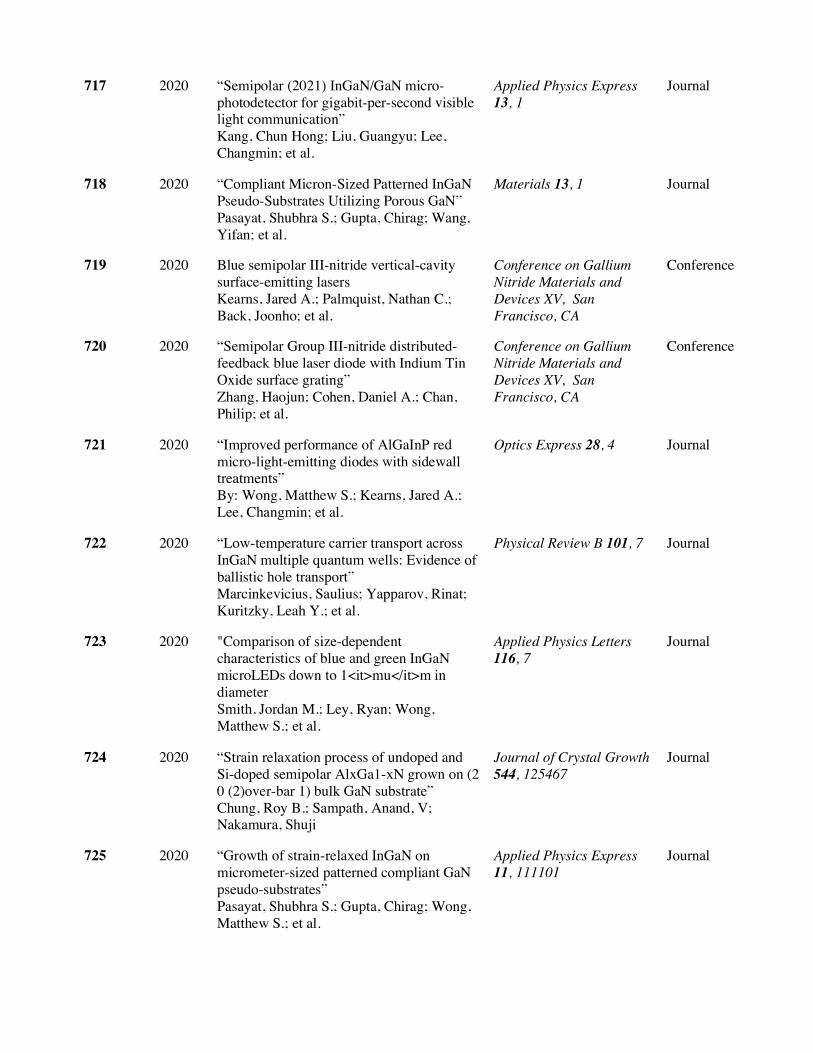
717 2020 “Semipolar (2021) InGaN/GaN micro-photodetector for gigabit-per-second visible light communication” Kang, Chun Hong; Liu, Guangyu; Lee, Changmin; et al.
Applied Physics Express 13, 1
Journal
718 2020 “Compliant Micron-Sized Patterned InGaN Pseudo-Substrates Utilizing Porous GaN” Pasayat, Shubhra S.; Gupta, Chirag; Wang, Yifan; et al.
Materials 13, 1 Journal
719 2020 Blue semipolar III-nitride vertical-cavity surface-emitting lasers Kearns, Jared A.; Palmquist, Nathan C.; Back, Joonho; et al.
Conference on Gallium Nitride Materials and Devices XV, San Francisco, CA
Conference
720 2020 “Semipolar Group III-nitride distributed-feedback blue laser diode with Indium Tin Oxide surface grating” Zhang, Haojun; Cohen, Daniel A.; Chan, Philip; et al.
Conference on Gallium Nitride Materials and Devices XV, San Francisco, CA
Conference
721 2020 “Improved performance of AlGaInP red micro-light-emitting diodes with sidewall treatments” By: Wong, Matthew S.; Kearns, Jared A.; Lee, Changmin; et al.
Optics Express 28, 4 Journal
722 2020 “Low-temperature carrier transport across InGaN multiple quantum wells: Evidence of ballistic hole transport” Marcinkevicius, Saulius; Yapparov, Rinat; Kuritzky, Leah Y.; et al.
Physical Review B 101, 7 Journal
723 2020 "Comparison of size-dependent characteristics of blue and green InGaN microLEDs down to 1<it>mu</it>m in diameter Smith, Jordan M.; Ley, Ryan; Wong, Matthew S.; et al.
Applied Physics Letters 116, 7
Journal
724 2020 “Strain relaxation process of undoped and Si-doped semipolar AlxGa1-xN grown on (2 0 (2)over-bar 1) bulk GaN substrate” Chung, Roy B.; Sampath, Anand, V; Nakamura, Shuji
Journal of Crystal Growth 544, 125467
Journal
725 2020 “Growth of strain-relaxed InGaN on micrometer-sized patterned compliant GaN pseudo-substrates” Pasayat, Shubhra S.; Gupta, Chirag; Wong, Matthew S.; et al.
Applied Physics Express 11, 111101
Journal
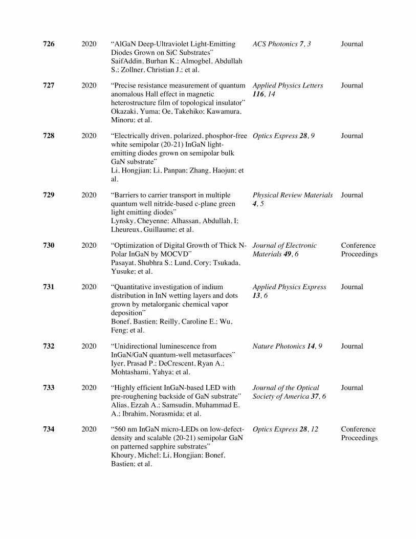
726 2020 “AlGaN Deep-Ultraviolet Light-Emitting Diodes Grown on SiC Substrates” SaifAddin, Burhan K.; Almogbel, Abdullah S.; Zollner, Christian J.; et al.
ACS Photonics 7, 3 Journal
727 2020 “Precise resistance measurement of quantum anomalous Hall effect in magnetic heterostructure film of topological insulator” Okazaki, Yuma; Oe, Takehiko; Kawamura, Minoru; et al.
Applied Physics Letters 116, 14
Journal
728 2020 “Electrically driven, polarized, phosphor-free white semipolar (20-21) InGaN light-emitting diodes grown on semipolar bulk GaN substrate” Li, Hongjian; Li, Panpan; Zhang, Haojun; et al.
Optics Express 28, 9 Journal
729 2020 “Barriers to carrier transport in multiple quantum well nitride-based c-plane green light emitting diodes” Lynsky, Cheyenne; Alhassan, Abdullah, I; Lheureux, Guillaume; et al.
Physical Review Materials 4, 5
Journal
730 2020 “Optimization of Digital Growth of Thick N-Polar InGaN by MOCVD” Pasayat, Shubhra S.; Lund, Cory; Tsukada, Yusuke; et al.
Journal of Electronic Materials 49, 6
Conference Proceedings
731 2020 “Quantitative investigation of indium distribution in InN wetting layers and dots grown by metalorganic chemical vapor deposition” Bonef, Bastien; Reilly, Caroline E.; Wu, Feng; et al.
Applied Physics Express 13, 6
Journal
732 2020 “Unidirectional luminescence from InGaN/GaN quantum-well metasurfaces” Iyer, Prasad P.; DeCrescent, Ryan A.; Mohtashami, Yahya; et al.
Nature Photonics 14, 9 Journal
733 2020 “Highly efficient InGaN-based LED with pre-roughening backside of GaN substrate” Alias, Ezzah A.; Samsudin, Muhammad E. A.; Ibrahim, Norasmida; et al.
Journal of the Optical Society of America 37, 6
Journal
734 2020 “560 nm InGaN micro-LEDs on low-defect-density and scalable (20-21) semipolar GaN on patterned sapphire substrates” Khoury, Michel; Li, Hongjian; Bonef, Bastien; et al.
Optics Express 28, 12 Conference Proceedings

735 2020 “Tamm plasmons in metal/nanoporous GaN distributed Bragg reflector cavities for active and passive optoelectronics” Lheureux, G.; Monavarian, M.; Anderson, R.; et al.
Optics Express 28, 12 Journal
736 2020 “Size-independent low voltage of InGaN micro-light-emitting diodes with epitaxial tunnel junctions using selective area growth by metalorganic chemical vapor deposition” Li, Panpan; Zhang, Haojun; Li, Hongjian; et al.
Optics Express 28, 13 Journal
737 “Revealing the importance of light extraction efficiency in InGaN/GaN microLEDs via chemical treatment and dielectric passivation” Ley, Ryan T.; Smith, Jordan M.; Wong, Matthew S.; et al.
Applied Physics Letters 116, 25
Journal
PATENTS: (last updated 1/29/19)
Patent Title
US PATENTS
5,290,393 Crystal growth method for gallium nitride-based compound semiconductor
5,334,277 Method of vapor-growing semiconductor crystal and apparatus for vapor-growing the same
5,433,169 Method of depositing a gallium nitride-based III-V group compound semiconductor crystal layer
5,468,678 Method of manufacturing P-type compound semiconductor
5,563,422 Gallium nitride-based III-V group compound semiconductor device and method of producing the same
5,578,839 Light-emitting gallium nitride-based compound semiconductor device
5,652,434 Gallium nitride-based III-V group compound semiconductor
5,734,182 Light-emitting gallium nitride-based compound semiconductor device
5,747,832 Light-emitting gallium nitride-based compound semiconductor device
5,767,581 Gallium nitride-based III-V group compound semiconductor
5,777,350 Nitride semiconductor light-emitting device
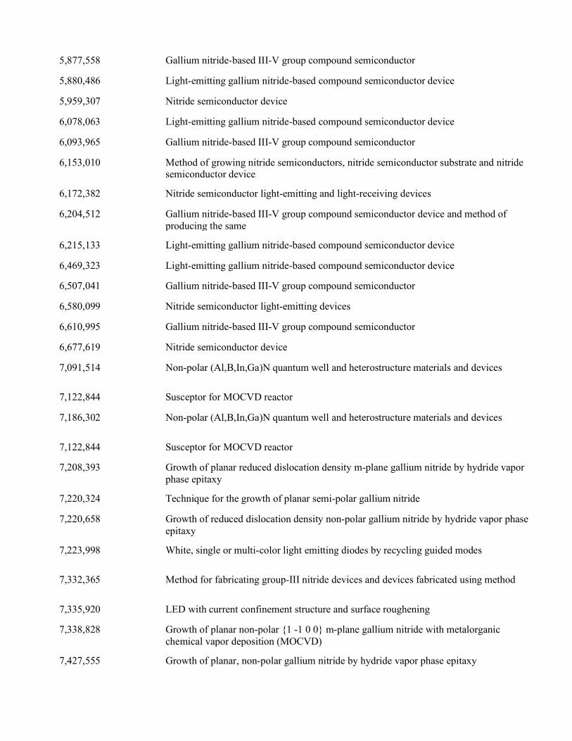
5,877,558 Gallium nitride-based III-V group compound semiconductor
5,880,486 Light-emitting gallium nitride-based compound semiconductor device
5,959,307 Nitride semiconductor device
6,078,063 Light-emitting gallium nitride-based compound semiconductor device
6,093,965 Gallium nitride-based III-V group compound semiconductor
6,153,010 Method of growing nitride semiconductors, nitride semiconductor substrate and nitride semiconductor device
6,172,382 Nitride semiconductor light-emitting and light-receiving devices
6,204,512 Gallium nitride-based III-V group compound semiconductor device and method of producing the same
6,215,133 Light-emitting gallium nitride-based compound semiconductor device
6,469,323 Light-emitting gallium nitride-based compound semiconductor device
6,507,041 Gallium nitride-based III-V group compound semiconductor
6,580,099 Nitride semiconductor light-emitting devices
6,610,995 Gallium nitride-based III-V group compound semiconductor
6,677,619 Nitride semiconductor device
7,091,514 Non-polar (Al,B,In,Ga)N quantum well and heterostructure materials and devices
7,122,844 Susceptor for MOCVD reactor
7,186,302 Non-polar (Al,B,In,Ga)N quantum well and heterostructure materials and devices
7,122,844 Susceptor for MOCVD reactor
7,208,393 Growth of planar reduced dislocation density m-plane gallium nitride by hydride vapor phase epitaxy
7,220,324 Technique for the growth of planar semi-polar gallium nitride
7,220,658 Growth of reduced dislocation density non-polar gallium nitride by hydride vapor phase epitaxy
7,223,998 White, single or multi-color light emitting diodes by recycling guided modes
7,332,365 Method for fabricating group-III nitride devices and devices fabricated using method
7,335,920 LED with current confinement structure and surface roughening
7,338,828 Growth of planar non-polar {1 -1 0 0} m-plane gallium nitride with metalorganic chemical vapor deposition (MOCVD)
7,427,555 Growth of planar, non-polar gallium nitride by hydride vapor phase epitaxy

7,480,322 Electrically-pumped (Ga,In,Al)N vertical-cavity surface-emitting laser
7,504,274 Fabrication of nonpolar indium gallium nitride thin films, heterostructures and devices by metalorganic chemical vapor deposition
7,518,159 Packaging technique for the fabrication of polarized light emitting diodes
7,550,395 7,575,947 7,687,293 7,687,813 7,691,658 7,704,331 7,704,763 7,709,284 7,719,020 7,723,746 7,755,172
Control of photoelectrochemical (PEC) etching by modification of the local electrochemical potential of the semiconductor structure relative to the electrolyte Method for enhancing growth of semipolar (Al,In,Ga,B)N via metalorganic chemical vapor deposition Method for enhancing growth of semipolar (Al,In,Ga,B)N via metalorganic chemical vapor deposition Standing transparent mirror-less (STML) light emitting diode Method for improved growth of semipolar (Al,In,Ga,B)N Technique for the growth of planar semi-polar gallium nitride Technique for the highly efficient gallium nitride based LED via surface roughening Method for deposition of Mg Doped (Al,In,Ga, B)N layers (AL, GA, IN)N and ZnO direct wafer bonding structure for optoelectronic applications and its fabrication method Packaging technique for the fabrication of polarized light emitting diodes Opto-electronic and electronic devices using N-face GaN substrate prepared with ammono thermal growth
7,768,024 7,781,789 7,839,903 7,842,527 7,846,757 7,847,280 7,847,293 7,858,996 7,868,341 7,956,360
Improved horizontal emitting, vertical emitting, beam shaped, DFB lasers over patterned substrate with multiple overgrowth Transparent mirror-less (TML) light emitting diode Optimization of laser bar orientation for nonpolar (Ga,Al,In,B)N diode lasers MOCVD growth of high performance M-plane GAN optical devices Technique for the growth and fabrication of semipolar (Ga,Al,In,B)N thin films, heterostructures, and devices Nonpolar III-Nitride light emitting diodes with long wavelength emission Growth of reduced dislocation density non-polar gallium nitride by hybrid vapor phaseepitaxy Method for growth of semipolar (Al,In,Ga,B) N optoelectronic devices Optical designs for high-efficacy white-light emitting diodes Growth of planar reduced dislocation density M-plane gallium nitride by hydride vapor phase epitaxy
7,956,371 High efficiency light emitting diode (LED)
7,982,208 Non-polar (Al,B,In,Ga)N quantum well and heterostructure materials and devices
7,994,527 High light extraction efficiency light emitting diode (LED)
8,022,423 Standing transparent mirrorless light emitting diode
8,044,383 Thin P-type gallium nitride and aluminum gallium nitride electron-blocking layer free gallium nitride-based light emitting diode

8,044,417 Enhancement of optical polarization of nitride light-emitting diodes by increased indium incorporation
8,053,264 Photoelectrochemical etching of P-type semiconductor heterostructures
8,080,469 Method for increasing the area of non-polar and semi-polar nitride substrates
8,084,763 Optoelectronic device based on non-polar and semi-polar aluminum indium nitride and aluminum indium gallium nitride alloys
8,097,481 Growth of non-polar M-plane III-nitride film using metalorganic chemical vapor deposition (MOCVD)
8,110,482 Miscute semipolar optoelectronic device
8,114,698 High light extraction efficiency nitride based light emitting diode by surface roughening
8,124,991 Light emitting diodes with high extraction efficiency
8,128,756 Technique for the growth of planar semi-polar gallium nitride
8,148,244 Lateral growth method for defect reduction of semipolar nitride films
8,148,713 Method for fabrication of semipolar-(A1,In,Ga,B)N-based light emitting diodes
8,158,947 Planar nonpolar m-plane group III nitride films grown on miscute substrates
8,178,373 MOCVD growth of high performance m-plane GaN optical devices
8,183,557 (Al, In, Ga, B)N device structures on a patterned substrate
8,188,458 Non-polar (Al,B,In,Ga)N quantum well and heterostructure materials and devices
8,193,079 Method for conductivity control of semipolar (Al,In,Ga,B) N
8,203,159 Method for growth of semipolar (Al,In,Ga,B) N optoelectronic devices
8,211,723 AlxGal-x-N-cladding-free nonpolar GaN-Based laser diodes and LED’s
8,227,818 Horizontal emitting, vertical emitting, beam shaped, DFB lasers fabricated by growth over patterned substrate with multiple overgrowth
8,227,819 Thin P-type GaN and AlGaN electron-blocking layer free GaN-based light emitting diodes
8,227,820 Semiconductor light-emitting device
8,253,221 Gallium nitride bulk crystals and their growth method
8,254,423 (Al, Ga, In) N Diode laser fabricated at reduced temperature

8,263,424 Opto-electronic and electronic devices using N-face GaN substrate prepared with ammonothermal growth
8,278,128 Enhancement of optical polarization of nitride light-emitting diodes by wafer miscute
8,294,166 Transparent LEDs
8,299,452 Method for fabrication of semipolar-(A1,In,Ga,B)N-based light emitting diodes
8,357,925 Optoelectronic Device Based on Non-Polar and Semi-Polr Aluminum Indium Nitride and aluminum Indium Gallium Nitride
8,368,109 Light emitting diodes with a p-type surface bonded to a transparent submount to increase light extraction efficiency
8,368,179 Method for improved growth of semipolar (al,in,ga,b)n
8,405,128 Method for enhancing growth of semipolar (al,in,ga,b)n via metalorganic chemical vapor deposition
8,481,991 Anisotropic strain control in semipolar nitride quantum wells by partially or fully relaxed aluminum indium gallium nitride
8,502,246 Fabrication of nonpolar indium gallium nitride thin films, heterostructures and devices by metalorganic chemical vapor
8,524,012 Technique for the growth of planar semi-polar gallium nitride
8,536,618 Light emitting diode structure utilizing zinc oxide nanorod arrays on one or more surfaces, and a low cost method of producing
8,541,869 Cleaved facet (Ga,Al,In)n edge-emitting laser diodes grown on semipolar {11-2n} bulk gan substrates
8,574,525 Using boron-containing compounds, gasses and fluids during ammonothermal growth of group-III nitride crystals
8,588,260 Optimization of laser bar orientation for nonpolar (Ga,Al,In,B)n diode lasers
8592802 (Al,In,Ga,B)n device structures on a patterned substrate
8,624,281 Optical designs for high-efficacy white-light emitting diodes
8,637,334 High brightness light emitting diode covered by zinc oxide layers on multiple surfaces grown in low temperature aqueous solute
8,641,823 Reactor Designs for use in Ammonthermal Growth of Group-III Nitride Crystals
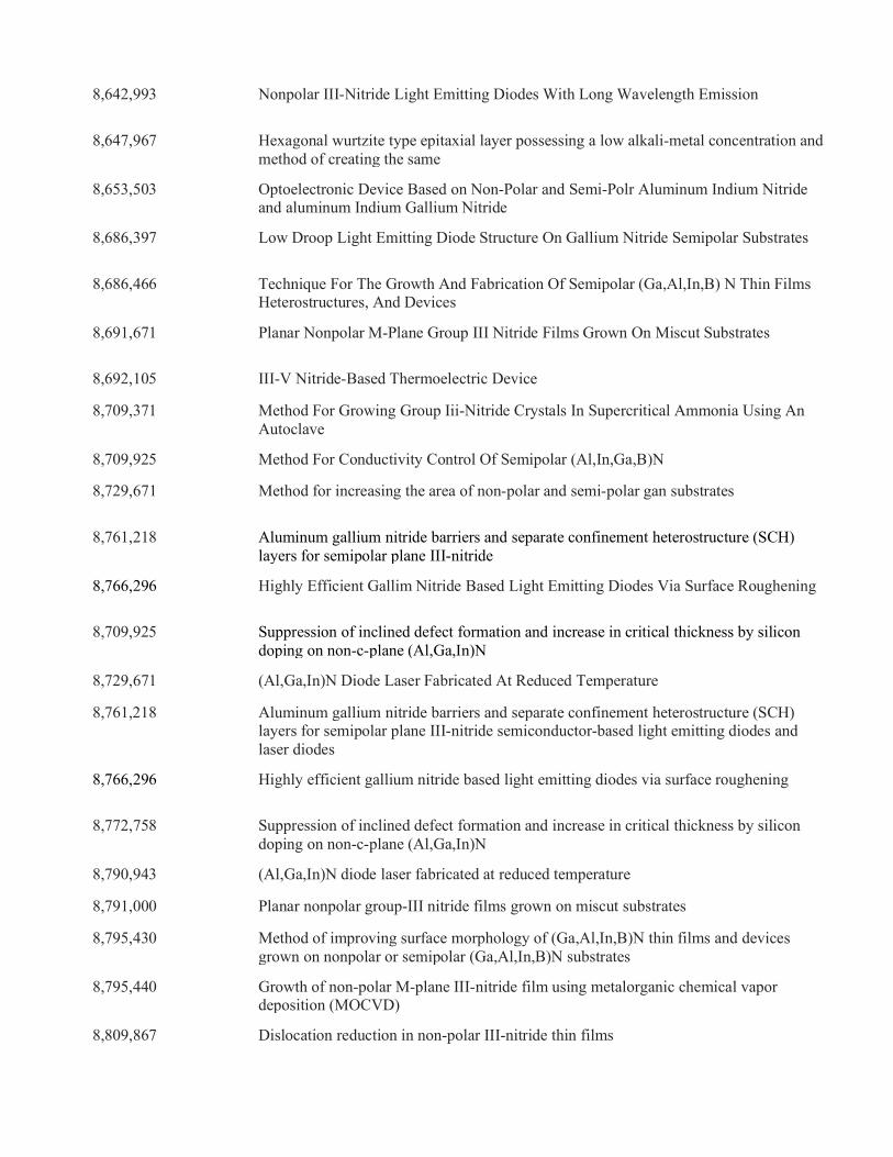
8,642,993 Nonpolar III-Nitride Light Emitting Diodes With Long Wavelength Emission
8,647,967 Hexagonal wurtzite type epitaxial layer possessing a low alkali-metal concentration and method of creating the same
8,653,503 Optoelectronic Device Based on Non-Polar and Semi-Polr Aluminum Indium Nitride and aluminum Indium Gallium Nitride
8,686,397 Low Droop Light Emitting Diode Structure On Gallium Nitride Semipolar Substrates
8,686,466 Technique For The Growth And Fabrication Of Semipolar (Ga,Al,In,B) N Thin Films Heterostructures, And Devices
8,691,671 Planar Nonpolar M-Plane Group III Nitride Films Grown On Miscut Substrates
8,692,105 III-V Nitride-Based Thermoelectric Device
8,709,371 Method For Growing Group Iii-Nitride Crystals In Supercritical Ammonia Using An Autoclave
8,709,925 Method For Conductivity Control Of Semipolar (Al,In,Ga,B)N
8,729,671 Method for increasing the area of non-polar and semi-polar gan substrates
8,761,218 Aluminum gallium nitride barriers and separate confinement heterostructure (SCH) layers for semipolar plane III-nitride
8,766,296 Highly Efficient Gallim Nitride Based Light Emitting Diodes Via Surface Roughening
8,709,925 Suppression of inclined defect formation and increase in critical thickness by silicon doping on non-c-plane (Al,Ga,In)N
8,729,671 (Al,Ga,In)N Diode Laser Fabricated At Reduced Temperature
8,761,218 Aluminum gallium nitride barriers and separate confinement heterostructure (SCH) layers for semipolar plane III-nitride semiconductor-based light emitting diodes and laser diodes
8,766,296 Highly efficient gallium nitride based light emitting diodes via surface roughening
8,772,758 Suppression of inclined defect formation and increase in critical thickness by silicon doping on non-c-plane (Al,Ga,In)N
8,790,943 (Al,Ga,In)N diode laser fabricated at reduced temperature
8,791,000 Planar nonpolar group-III nitride films grown on miscut substrates
8,795,430 Method of improving surface morphology of (Ga,Al,In,B)N thin films and devices grown on nonpolar or semipolar (Ga,Al,In,B)N substrates
8,795,440 Growth of non-polar M-plane III-nitride film using metalorganic chemical vapor deposition (MOCVD)
8,809,867 Dislocation reduction in non-polar III-nitride thin films

8,835,200 High light extraction efficiency nitride based light emitting diode by surface roughening
8,835,959 Transparent light emitting diodes
8,841,691 Light emitting diode structure utilizing zinc oxide nanorod arrays on one or more surfaces, and a low cost method of producing
8,853,669 Limiting strain relaxation in III-nitride heterostructures by substrate and epitaxial layer patterning
8,860,051 Textured phosphor conversion layer light emitting diode
8,866,126 Anisotropic Strain Control In Semipolar Nitride Quantum Wells By Partially Or Fully Relaxed Aluminum Indium Gallium Nitride
8,866,149 Method For The Reuse Of Gallium Nitride Epitaxial Substrates
8,882,935 Fabrication of nonpolar indium gallium nitride thin films, heterostructures and devices by metalorganic chemical vapor
8,956,896 Metalorganic Chemical Vapor Deposition (Mocvd) Growth Of High Performance Non-Polar III-Nitride Optical Devices
9,039,834 Non-polar gallium nitride thin films grown by metalorganic chemical vapor deposition
9,040,326 High Light Extraction Efficiency Nitride Based Light Emitting Diode By Surface Roughening
9,040,327 Alxgal-X-N-Cladding-Free Nonpolar III-Nitride Based Laser Diodes And Light Emitting Diodes
9,054,498 (Al,Ga,In)N Diode Laser Fabricated At Reduced (Al,Ga,In)N Diode Laser Fabricated At Reduced Temperature
9,077,151 Semi-Polar III-Nitride Optoelectronic Devices On M-Plane Substrates With Miscuts Less Than +/-15 Degrees In The C-Direction
9,130,119 Non-Polar And Semi-Polar Light Emitting Devices
9,133,564 Ammonothermal Growth Of Group-Iii Nitride Crystals On Seeds With At Least Two Surfaces Making An Acute, Right Or Obtuse
9,136,673 Structure and method for the fabrication of a gallium nitride vertical cavity surface emitting laser
9,147,733 Method For The Reuse Of Gallium Nitride Epitaxial Substrates
9,159,553 Semipolar nitride-based devices on partially or fully relaxed alloys with misfit dislocations at the heterointerface
9,219,205 Optical Designs For High-Efficacy White-Light Emitting Diodes
9,231,376 Technique For The Growth And Fabrication Of Semipolar (Ga,Al,In,B) N Thin Films Heterostructures, And Devices
9,240,529 Textured Phosphor Conversion Layer Light Emitting Diode
9,243,344 Gallium Nitride Bulk Crystals And Their Growth Method
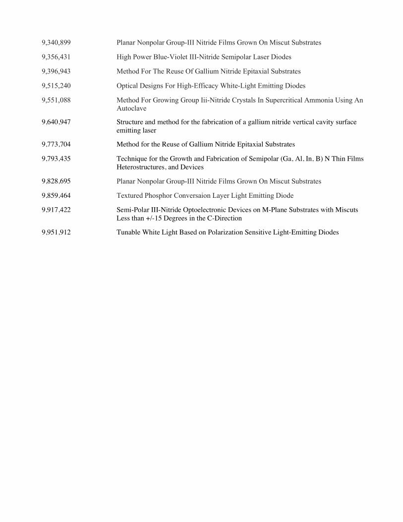
9,340,899 Planar Nonpolar Group-III Nitride Films Grown On Miscut Substrates
9,356,431 High Power Blue-Violet III-Nitride Semipolar Laser Diodes
9,396,943 Method For The Reuse Of Gallium Nitride Epitaxial Substrates
9,515,240 Optical Designs For High-Efficacy White-Light Emitting Diodes
9,551,088 Method For Growing Group Iii-Nitride Crystals In Supercritical Ammonia Using An Autoclave
9,640,947 Structure and method for the fabrication of a gallium nitride vertical cavity surface emitting laser
9,773,704 Method for the Reuse of Gallium Nitride Epitaxial Substrates
9,793,435 Technique for the Growth and Fabrication of Semipolar (Ga, Al, In, B) N Thin Films Heterostructures, and Devices
9,828,695 Planar Nonpolar Group-III Nitride Films Grown On Miscut Substrates
9,859,464 Textured Phosphor Conversaion Layer Light Emitting Diode
9,917,422 Semi-Polar III-Nitride Optoelectronic Devices on M-Plane Substrates with Miscuts Less than +/-15 Degrees in the C-Direction
9,951,912 Tunable White Light Based on Polarization Sensitive Light-Emitting Diodes
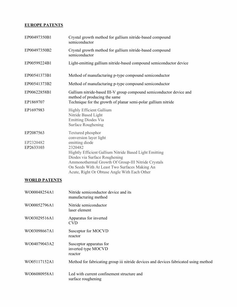
EUROPE PATENTS
EP00497350B1 Crystal growth method for gallium nitride-based compound semiconductor
EP00497350B2 Crystal growth method for gallium nitride-based compound semiconductor
EP00599224B1 Light-emitting gallium nitride-based compound semiconductor device
EP00541373B1 Method of manufacturing p-type compound semiconductor
EP00541373B2 Method of manufacturing p-type compound semiconductor
EP00622858B1 EP1869707
Gallium nitride-based III-V group compound semiconductor device and method of producing the same Technique for the growth of planar semi-polar gallium nitride
EP1697983 Highly Efficient Gallium Nitride Based Light Emitting Diodes Via Surface Roughening
EP2087563 EP2320482 EP2633103
Textured phosphor conversion layer light emitting diode 2320482 Hightly Efficient Gallium Nitride Based Light Emitting Diodes via Surface Roughening Ammonothermal Growth Of Group-III Nitride Crystals On Seeds With At Least Two Surfaces Making An Acute, Right Or Obtuse Angle With Each Other
WORLD PATENTS
WO00048254A1 Nitride semiconductor device and its manufacturing method
WO00052796A1 Nitride semiconductor laser element
WO03029516A1 Apparatus for inverted CVD
WO03098667A1 Susceptor for MOCVD reactor
WO04079043A2 Susceptor apparatus for inverted type MOCVD reactor
WO05117152A1 Method for fabricating group iii nitride devices and devices fabricated using method
WO06080958A1 Led with current confinement structure and surface roughening
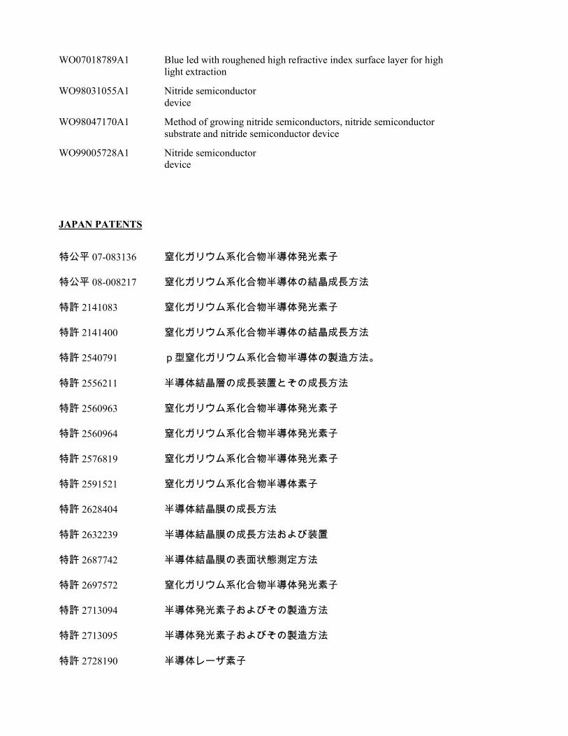
WO07018789A1 Blue led with roughened high refractive index surface layer for high light extraction
WO98031055A1 Nitride semiconductor device
WO98047170A1 Method of growing nitride semiconductors, nitride semiconductor substrate and nitride semiconductor device
WO99005728A1 Nitride semiconductor device
JAPAN PATENTS
特公平 07-083136 窒化ガリウム系化合物半導体発光素子
特公平 08-008217 窒化ガリウム系化合物半導体の結晶成長方法
特許 2141083 窒化ガリウム系化合物半導体発光素子
特許 2141400 窒化ガリウム系化合物半導体の結晶成長方法
特許 2540791 p型窒化ガリウム系化合物半導体の製造方法。
特許 2556211 半導体結晶層の成長装置とその成長方法
特許 2560963 窒化ガリウム系化合物半導体発光素子
特許 2560964 窒化ガリウム系化合物半導体発光素子
特許 2576819 窒化ガリウム系化合物半導体発光素子
特許 2591521 窒化ガリウム系化合物半導体素子
特許 2628404 半導体結晶膜の成長方法
特許 2632239 半導体結晶膜の成長方法および装置
特許 2687742 半導体結晶膜の表面状態測定方法
特許 2697572 窒化ガリウム系化合物半導体発光素子
特許 2713094 半導体発光素子およびその製造方法
特許 2713095 半導体発光素子およびその製造方法
特許 2728190 半導体レーザ素子
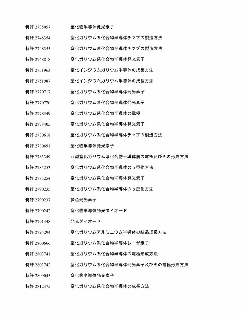
特許 2735057 窒化物半導体発光素子
特許 2748354 窒化ガリウム系化合物半導体チップの製造方法
特許 2748355 窒化ガリウム系化合物半導体チップの製造方法
特許 2748818 窒化ガリウム系化合物半導体発光素子
特許 2751963 窒化インジウムガリウム半導体の成長方法
特許 2751987 窒化インジウムガリウム半導体の成長方法
特許 2770717 窒化ガリウム系化合物半導体発光素子
特許 2770720 窒化ガリウム系化合物半導体発光素子
特許 2778349 窒化ガリウム系化合物半導体の電極
特許 2778405 窒化ガリウム系化合物半導体発光素子
特許 2780618 窒化ガリウム系化合物半導体チップの製造方法
特許 2780691 窒化物半導体発光素子
特許 2783349 n型窒化ガリウム系化合物半導体層の電極及びその形成方法
特許 2785253 窒化ガリウム系化合物半導体のp型化方法
特許 2785254 窒化ガリウム系化合物半導体発光素子
特許 2790235 窒化ガリウム系化合物半導体のp型化方法
特許 2790237 多色発光素子
特許 2790242 窒化物半導体発光ダイオード
特許 2791448 発光ダイオード
特許 2795294 窒化ガリウムアルミニウム半導体の結晶成長方法。
特許 2800666 窒化ガリウム系化合物半導体レーザ素子
特許 2803741 窒化ガリウム系化合物半導体の電極形成方法
特許 2803742 窒化ガリウム系化合物半導体発光素子及びその電極形成方法
特許 2809045 窒化物半導体発光素子
特許 2812375 窒化ガリウム系化合物半導体の成長方法
特許 2827794 p型窒化ガリウムの成長方法
特許 2828187 窒化ガリウム系化合物半導体発光素子
特許 2836685 p型窒化ガリウム系化合物半導体の製造方法
特許 2836686 窒化ガリウム系化合物半導体発光素子
特許 2836687 窒化ガリウム系化合物半導体発光素子
特許 2859478 発光デバイス用の窒化ガリウム系化合物半導体ウエハーの切断方法
特許 2861991 窒化ガリウム系化合物半導体チップの製造方法
特許 2868081 窒化ガリウム系化合物半導体発光素子
特許 2890390 窒化ガリウム系化合物半導体発光素子
特許 2890392 III-V族窒化物半導体発光素子
特許 2890396 窒化物半導体発光素子
特許 2891348 窒化物半導体レーザ素子
特許 2900928 発光ダイオード
特許 2900990 窒化物半導体発光素子
特許 2910023 窒化ガリウム系化合物半導体発光素子
特許 2910811 窒化ガリウム系化合物半導体ウエハーの切断方法
特許 2914014 窒化ガリウム系化合物半導体チップの製造方法
特許 2914065 青色発光素子及びその製造方法
特許 2917742 窒化ガリウム系化合物半導体発光素子とその製造方法
特許 2918139 窒化ガリウム系化合物半導体発光素子
特許 2921746 窒化物半導体レーザ素子
特許 3346735 窒化物半導体発光素子及びその製造方法
特許 2932467 窒化ガリウム系化合物半導体発光素子
特許 2932468 窒化ガリウム系化合物半導体発光素子
特許 2947047 LEDチップのリードフレームへのダイボンド方法
特許 2953326 窒化ガリウム系化合物半導体レーザ素子の製造方法
特許 2956489 窒化ガリウム系化合物半導体の結晶成長方法
特許 2964822 発光ダイオードの製造方法
特許 2976951 窒化物半導体発光ダイオードを備えた表示装置
特許 2982553 発光デバイスの製造方法
特許 2985908 窒化ガリウム系化合物半導体の結晶成長方法
特許 2998696 発光ダイオード
特許 3009091 青色発光ダイオード
特許 3009095 窒化物半導体発光素子
特許 3019132 窒化ガリウム系化合物半導体受光素子
特許 3036465 発光ダイオードを用いたディスプレイ
特許 3047960 n型窒化物半導体の電極
特許 3077781 窒化インジウムガリウムの成長方法
特許 3087829 窒化物半導体素子の製造方法
特許 3087831 窒化物半導体素子
特許 3091593 窒化物半導体発光デバイス用積層体
特許 3101997 窒化物半導体レーザ素子
特許 3129384 窒化物半導体レーザ素子
特許 3135041 窒化物半導体発光素子
特許 3141824 窒化物半導体発光素子
特許 3152238 発光ダイオード
特許 3154364 n型窒化ガリウム系化合物半導体層の電極及びその形成方法
特許 3180710 窒化ガリウム系化合物半導体発光素子の製造方法
特許 3180871 窒化ガリウム系化合物半導体発光素子およびその電極形成方法
特許 3187284 n型窒化物半導体層の電極
特許 3203282 発光デバイス用窒化インジウムガリウム半導体
特許 3209233 青色発光ダイオードおよびその製造方法
特許 3212008 窒化ガリウム系化合物半導体レーザ素子
特許 3216118 窒化物半導体素子及びその製造方法
特許 3218595 窒化物半導体レーザ素子及びその製造方法
特許 3216596 窒化ガリウム系化合物半導体発光素子
特許 3218963 窒化物半導体レーザ素子及びその製造方法
特許 3220977 窒化物半導体レーザ素子及び窒化物半導体レーザ素子の製造方法。
特許 3223810 窒化ガリウム系化合物半導体発光素子
特許 3223832 窒化物半導体素子及び半導体レーザダイオード
特許 3224020 窒化物半導体発光素子およびその製造方法
特許 3227287 窒化ガリウム系化合物半導体チップの製造方法と窒化ガリウム系化合物半導体素子
特許 3233258 窒化物半導体の電極
特許 3235440 窒化物半導体レーザ素子とその製造方法
特許 3241250 窒化物半導体レーザ素子
特許 3248564 窒化物半導体レーザダイオード
特許 3255224 窒化ガリウム系化合物半導体素子及びその製造方法
特許 3257344 窒化ガリウム系化合物半導体の結晶成長方法
特許 3257498 窒化ガリウム系化合物半導体の結晶成長方法
特許 3259811 窒化物半導体素子の製造方法及び窒化物半導体素子
特許 3267250 窒化物半導体発光素子
特許 3269070 窒化物半導体発光素子
特許 3271645 窒化物半導体発光ダイオード
特許 3271657 n型窒化ガリウム系化合物半導体の電極及びその形成方法
特許 3272588 窒化物半導体レーザ素子
特許 3274907 窒化インジウムガリウム化合物半導体の成長方法
特許 3275810 窒化物半導体発光素子
特許 3278108 窒化物半導体レーザ素の製造方法
特許 3282174 窒化物半導体発光素子
特許 3282175 窒化物半導体素子
特許 3292083 窒化物半導体基板の製造方法及び窒化物半導体素子の製造方法
特許 3298390 窒化物半導体多色発光素子の製造方法
特許 3298454 窒化ガリウム系化合物半導体発光素子の製造方法
特許 3301345 p型窒化ガリウム系化合物半導体層の形成方法
特許 3301601 窒化物半導体発光素子
特許 3303645 窒化物半導体発光素子の製造方法
特許 3307218 窒化物半導体レーザ素子の製造方法
特許 3309953 窒化物半導体レーザダイオード
特許 3314620 窒化物半導体発光素子
特許 3314641 窒化物半導体レーザ素子
特許 3314666 窒化物半導体素子
特許 3314671 窒化物半導体素子
特許 3319585 窒化物半導体レーザ素子の製造方法
特許 3327170 発光ダイオードの製造方法
特許 3327179 窒化物半導体レーザ素子の製造方法
特許 3329753 窒化物半導体レーザ素子
特許 3334624 窒化物半導体レーザ素子
特許 3336599 窒化物半導体レーザ素子
特許 3339049 窒化物半導体レーザ素子
特許 3460581 窒化物半導体の成長方法及び窒化物半導体素子
特許 3272588 窒化物半導体レーザ素子
特許 3274907 窒化インジウムガリウム化合物半導体の成長方法
特許 3275810 窒化物半導体発光素子
特許 3278108 窒化物半導体レーザ素の製造方法
特許 3282174 窒化物半導体発光素子
特許 3282175 窒化物半導体素子
特許 3292083 窒化物半導体基板の製造方法及び窒化物半導体素子の製造方法
特許 3298390 窒化物半導体多色発光素子の製造方法
特許 3298454 窒化ガリウム系化合物半導体発光素子の製造方法
特許 3301345 p型窒化ガリウム系化合物半導体層の形成方法
特許 3301601 窒化物半導体発光素子
特許 3303645 窒化物半導体発光素子の製造方法
特許 3307218 窒化物半導体レーザ素子の製造方法
特許 3309953 窒化物半導体レーザダイオード
特許 3314620 窒化物半導体発光素子
特許 3314641 窒化物半導体レーザ素子
特許 3314666 窒化物半導体素子
特許 3314671 窒化物半導体素子
特許 3319585 窒化物半導体レーザ素子の製造方法
特許 3327170 発光ダイオードの製造方法
特許 3327179 窒化物半導体レーザ素子の製造方法
特許 3329753 窒化物半導体レーザ素子
特許 3334624 窒化物半導体レーザ素子
特許 3336599 窒化物半導体レーザ素子
特許 3339049 窒化物半導体レーザ素子
特許 3344056 窒化ガリウム系化合物半導体発光素子及びその製造方法
特許 3344414 発光ダイオードを用いたディスプレイ
特許 3360812 窒化物半導体素子
特許 3366188 窒化物半導体素子
特許 3366586 発光ダイオード
特許 3369089 窒化ガリウム系化合物半導体発光素子
特許 3371830 窒化物半導体発光素子
特許 3372226 窒化物半導体レーザ素子
特許 3374737 窒化物半導体素子
特許 3379619 窒化物半導体レーザ素子
特許 3395631 窒化物半導体素子及び窒化物半導体素子の製造方法
特許 3405334 窒化物半導体素子
特許 3424465 窒化物半導体素子及び窒化物半導体の成長方法
特許 3431389 窒化物半導体レーザ素子
特許 3433730 窒化物半導体発光素子
特許 3434162 窒化物半導体素子
特許 3438675 窒化物半導体の成長方法
特許 3441883 窒化物半導体レーザ素子
特許 3448196 窒化物半導体発光素子
特許 3454355 窒化ガリウム系化合物半導体発光素子
特許 3456413 窒化物半導体の成長方法及び窒化物半導体素子
特許 3468082 窒化物半導体素子
特許 3470712 窒化物半導体レーザ素子
特許 3473595 発光デバイス
特許 3476636 窒化物半導体レーザ素子
特許 3478090 窒化物半導体素子
特許 3478287 窒化ガリウム系化合物半導体の結晶成長方法と窒化ガリウム系化合物半導体

特許 3482955 窒化ガリウム系化合物半導体発光素子
特許 3484842 窒化物半導体レーザ素子
特許 3484997 窒化ガリウム系化合物半導体発光素子
特許 3496480 窒化物半導体素子
特許 3496512 窒化物半導体素子
特許 3502527 窒化物半導体レーザ素子
特許 3505167 窒化ガリウム系化合物半導体発光素子の製造方法
特許 3511970 窒化物半導体発光素子
特許 3523700 窒化物半導体レーザ素子
特許 3529286 窒化物半導体レーザ素子の製造方法
特許 3537977 窒化物半導体レーザ素子の製造方法
特許 3537984 窒化物半導体レーザ素子
特許 3538275 窒化物半導体発光素子
特許 3548442 窒化ガリウム系化合物半導体発光素子
特許 3551751 窒化物半導体の成長方法
特許 3557894 窒化物半導体基板および窒化物半導体素子
特許 3562455 窒化物半導体レーザ素子の形成方法
特許 3565202 窒化物半導体レーザ素子
特許 3593952 窒化物半導体レーザ素子
特許 3604205 窒化物半導体の成長方法
特許 3604278 窒化物半導体レーザー素子
特許 3617565 窒化物半導体レーザ素子
特許 3620292 窒化物半導体素子
特許 3622045 窒化物半導体レーザ素子及びその製造方法
特許 3645207 発光ダイオード
特許 3646649 窒化ガリウム系化合物半導体発光素子
特許 3647236 窒化物半導体レーザ素子
特許 3651260 窒化物半導体素子
特許 3656454 窒化物半導体レーザ素子
特許 3657795 発光素子
特許 3658112 窒化物半導体レーザダイオード
特許 3658892 p型窒化物半導体の成長方法及び窒化物半導体素子
特許 3659050 窒化物半導体の成長方法及び窒化物半導体素子
特許 3660446 窒化物半導体素子及びその製造方法
特許 3669848 窒化物半導体レーザ素子
特許 3679626 窒化ガリウム系化合物半導体チップ
特許 3685682 窒化物半導体レーザ素子
特許 3705047 窒化物半導体発光素子
特許 3724490 発光ダイオード
特許 3724498 発光ダイオード
特許 3744211 窒化物半導体素子
特許 3758562 窒化物半導体多色発光素子
特許 3767491 窒化ガリウム系化合物半導体発光素子
特許 3767534 発光デバイス
特許 3770014 窒化物半導体素子
特許 3772651 窒化物半導体レーザ素子
特許 3772807 窒化ガリウム系化合物半導体発光素子
特許 3775259 窒化物半導体レーザ素子
特許 3786000 窒化物半導体レーザダイオードとその製造方法
特許 3794530 窒化物半導体レーザ素子
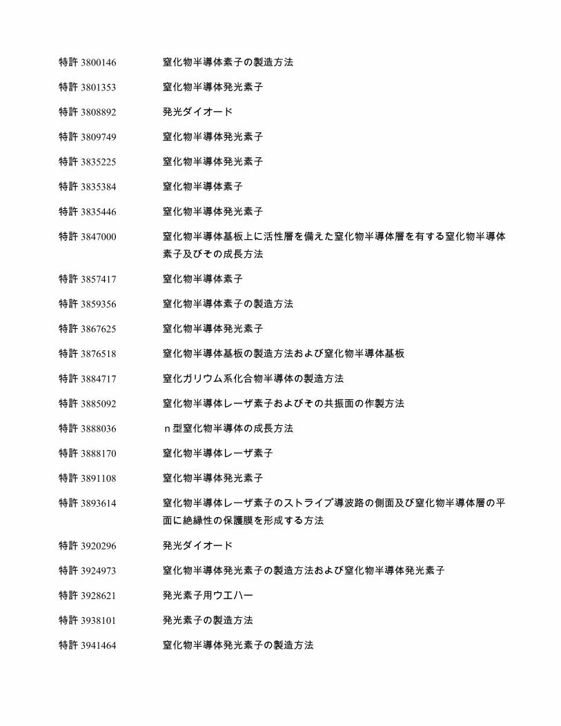
特許 3800146 窒化物半導体素子の製造方法
特許 3801353 窒化物半導体発光素子
特許 3808892 発光ダイオード
特許 3809749 窒化物半導体発光素子
特許 3835225 窒化物半導体発光素子
特許 3835384 窒化物半導体素子
特許 3835446 窒化物半導体発光素子
特許 3847000 窒化物半導体基板上に活性層を備えた窒化物半導体層を有する窒化物半導体素子及びその成長方法
特許 3857417 窒化物半導体素子
特許 3859356 窒化物半導体素子の製造方法
特許 3867625 窒化物半導体発光素子
特許 3876518 窒化物半導体基板の製造方法および窒化物半導体基板
特許 3884717 窒化ガリウム系化合物半導体の製造方法
特許 3885092 窒化物半導体レーザ素子およびその共振面の作製方法
特許 3888036 n型窒化物半導体の成長方法
特許 3888170 窒化物半導体レーザ素子
特許 3891108 窒化物半導体発光素子
特許 3893614 窒化物半導体レーザ素子のストライプ導波路の側面及び窒化物半導体層の平面に絶縁性の保護膜を形成する方法
特許 3920296 発光ダイオード
特許 3924973 窒化物半導体発光素子の製造方法および窒化物半導体発光素子
特許 3928621 発光素子用ウエハー
特許 3938101 発光素子の製造方法
特許 3941464 窒化物半導体発光素子の製造方法
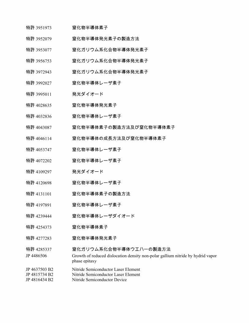
特許 3951973 窒化物半導体素子
特許 3952079 窒化物半導体発光素子の製造方法
特許 3953077 窒化ガリウム系化合物半導体発光素子
特許 3956753 窒化ガリウム系化合物半導体発光素子
特許 3972943 窒化ガリウム系化合物半導体発光素子
特許 3992027 窒化物半導体レーザ素子
特許 3995011 発光ダイオード
特許 4028635 窒化物半導体発光素子
特許 4032836 窒化物半導体レーザ素子
特許 4043087 窒化物半導体素子の製造方法及び窒化物半導体素子
特許 4046114 窒化物半導体の成長方法及び窒化物半導体素子
特許 4053747 窒化物半導体レーザ素子
特許 4072202 窒化物半導体レーザ素子
特許 4109297 発光ダイオード
特許 4120698 窒化物半導体レーザ素子
特許 4131101 窒化物半導体素子の製造方法
特許 4197891 窒化物半導体レーザ素子
特許 4239444 窒化物半導体レーザダイオード
特許 4254373 窒化物半導体素子
特許 4277283 窒化物半導体発光素子
特許 4285337 JP 4486506
窒化ガリウム系化合物半導体ウエハーの製造方法 Growth of reduced dislocation density non-polar gallium nitride by hydrid vapor phase epitaxy
JP 4637503 B2 JP 4815734 B2 JP 4816434 B2
Nitride Semiconductor Laser Element Nitride Semiconductor Laser Element Nitride Semiconductor Device
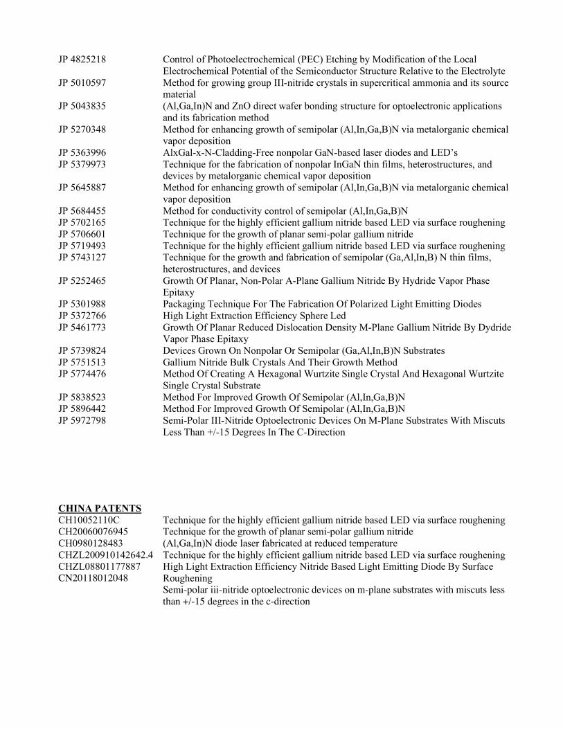
JP 4825218 JP 5010597 JP 5043835 JP 5270348 JP 5363996 JP 5379973 JP 5645887 JP 5684455 JP 5702165 JP 5706601 JP 5719493 JP 5743127 JP 5252465 JP 5301988 JP 5372766 JP 5461773 JP 5739824 JP 5751513 JP 5774476 JP 5838523 JP 5896442 JP 5972798
Control of Photoelectrochemical (PEC) Etching by Modification of the Local Electrochemical Potential of the Semiconductor Structure Relative to the Electrolyte Method for growing group III-nitride crystals in supercritical ammonia and its source material (Al,Ga,In)N and ZnO direct wafer bonding structure for optoelectronic applications and its fabrication method Method for enhancing growth of semipolar (Al,In,Ga,B)N via metalorganic chemical vapor deposition AlxGal-x-N-Cladding-Free nonpolar GaN-based laser diodes and LED’s Technique for the fabrication of nonpolar InGaN thin films, heterostructures, and devices by metalorganic chemical vapor deposition Method for enhancing growth of semipolar (Al,In,Ga,B)N via metalorganic chemical vapor deposition Method for conductivity control of semipolar (Al,In,Ga,B)N Technique for the highly efficient gallium nitride based LED via surface roughening Technique for the growth of planar semi-polar gallium nitride Technique for the highly efficient gallium nitride based LED via surface roughening Technique for the growth and fabrication of semipolar (Ga,Al,In,B) N thin films, heterostructures, and devices Growth Of Planar, Non-Polar A-Plane Gallium Nitride By Hydride Vapor Phase Epitaxy Packaging Technique For The Fabrication Of Polarized Light Emitting Diodes High Light Extraction Efficiency Sphere Led Growth Of Planar Reduced Dislocation Density M-Plane Gallium Nitride By Dydride Vapor Phase Epitaxy Devices Grown On Nonpolar Or Semipolar (Ga,Al,In,B)N Substrates Gallium Nitride Bulk Crystals And Their Growth Method Method Of Creating A Hexagonal Wurtzite Single Crystal And Hexagonal Wurtzite Single Crystal Substrate Method For Improved Growth Of Semipolar (Al,In,Ga,B)N Method For Improved Growth Of Semipolar (Al,In,Ga,B)N Semi-Polar III-Nitride Optoelectronic Devices On M-Plane Substrates With Miscuts Less Than +/-15 Degrees In The C-Direction
CHINA PATENTS CH10052110C CH20060076945 CH0980128483 CHZL200910142642.4 CHZL08801177887 CN20118012048
Technique for the highly efficient gallium nitride based LED via surface roughening Technique for the growth of planar semi-polar gallium nitride (Al,Ga,In)N diode laser fabricated at reduced temperature Technique for the highly efficient gallium nitride based LED via surface roughening High Light Extraction Efficiency Nitride Based Light Emitting Diode By Surface Roughening Semi-polar iii-nitride optoelectronic devices on m-plane substrates with miscuts less than +/-15 degrees in the c-direction
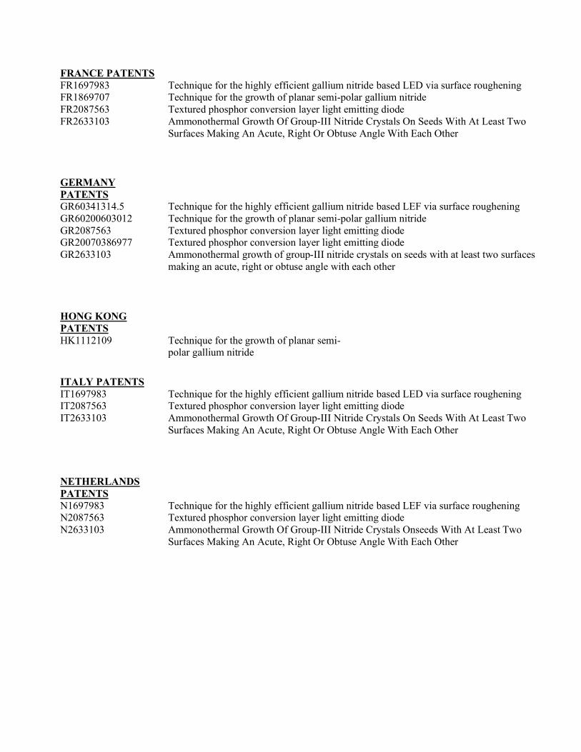
FRANCE PATENTS FR1697983 FR1869707 FR2087563 FR2633103
Technique for the highly efficient gallium nitride based LED via surface roughening Technique for the growth of planar semi-polar gallium nitride Textured phosphor conversion layer light emitting diode Ammonothermal Growth Of Group-III Nitride Crystals On Seeds With At Least Two Surfaces Making An Acute, Right Or Obtuse Angle With Each Other
GERMANY PATENTS GR60341314.5 GR60200603012 GR2087563 GR20070386977 GR2633103
Technique for the highly efficient gallium nitride based LEF via surface roughening Technique for the growth of planar semi-polar gallium nitride Textured phosphor conversion layer light emitting diode Textured phosphor conversion layer light emitting diode Ammonothermal growth of group-III nitride crystals on seeds with at least two surfaces making an acute, right or obtuse angle with each other
HONG KONG PATENTS HK1112109
Technique for the growth of planar semi-polar gallium nitride
ITALY PATENTS IT1697983 IT2087563 IT2633103
Technique for the highly efficient gallium nitride based LED via surface roughening Textured phosphor conversion layer light emitting diode Ammonothermal Growth Of Group-III Nitride Crystals On Seeds With At Least Two Surfaces Making An Acute, Right Or Obtuse Angle With Each Other
NETHERLANDS PATENTS N1697983 N2087563 N2633103
Technique for the highly efficient gallium nitride based LEF via surface roughening Textured phosphor conversion layer light emitting diode Ammonothermal Growth Of Group-III Nitride Crystals Onseeds With At Least Two Surfaces Making An Acute, Right Or Obtuse Angle With Each Other
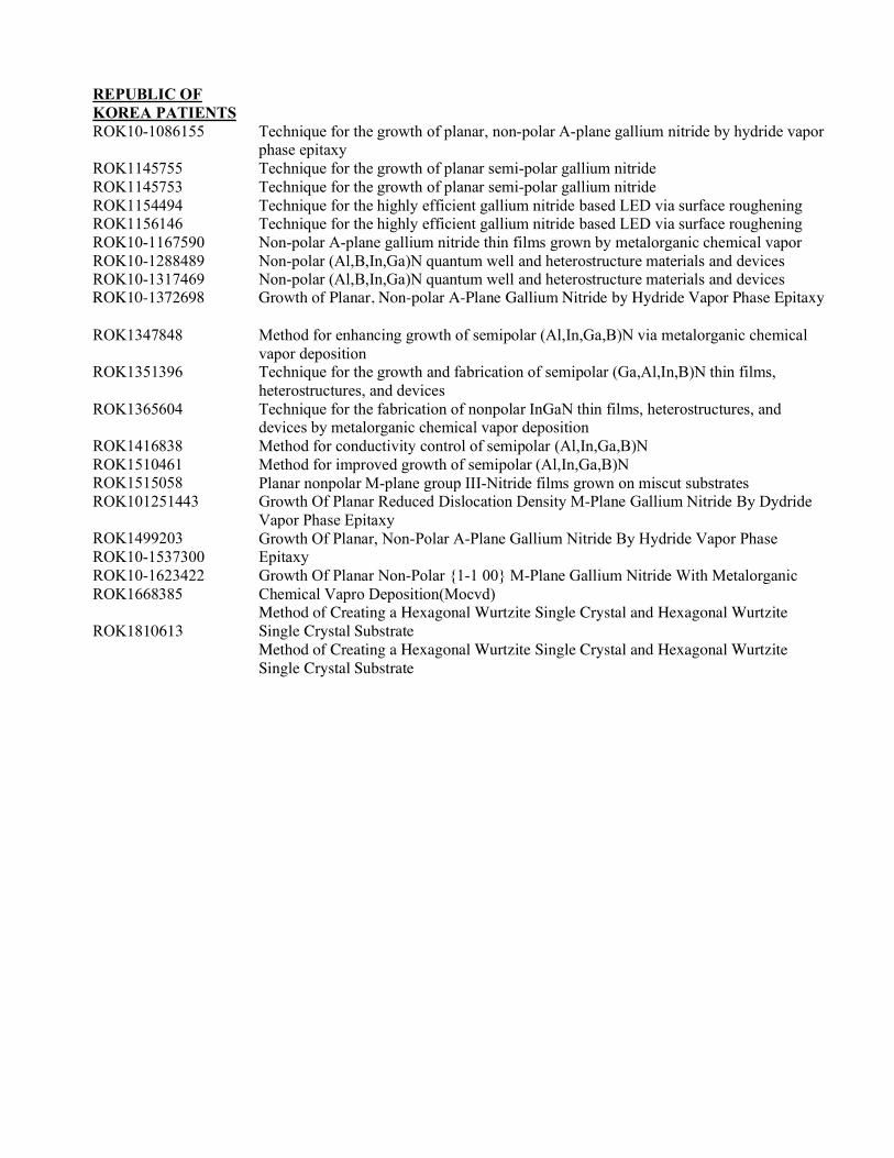
REPUBLIC OF KOREA PATIENTS ROK10-1086155 ROK1145755 ROK1145753 ROK1154494 ROK1156146 ROK10-1167590 ROK10-1288489 ROK10-1317469 ROK10-1372698 ROK1347848 ROK1351396 ROK1365604 ROK1416838 ROK1510461 ROK1515058 ROK101251443 ROK1499203 ROK10-1537300 ROK10-1623422 ROK1668385 ROK1810613
Technique for the growth of planar, non-polar A-plane gallium nitride by hydride vapor phase epitaxy Technique for the growth of planar semi-polar gallium nitride Technique for the growth of planar semi-polar gallium nitride Technique for the highly efficient gallium nitride based LED via surface roughening Technique for the highly efficient gallium nitride based LED via surface roughening Non-polar A-plane gallium nitride thin films grown by metalorganic chemical vapor Non-polar (Al,B,In,Ga)N quantum well and heterostructure materials and devices Non-polar (Al,B,In,Ga)N quantum well and heterostructure materials and devices Growth of Planar, Non-polar A-Plane Gallium Nitride by Hydride Vapor Phase Epitaxy Method for enhancing growth of semipolar (Al,In,Ga,B)N via metalorganic chemical vapor deposition Technique for the growth and fabrication of semipolar (Ga,Al,In,B)N thin films, heterostructures, and devices Technique for the fabrication of nonpolar InGaN thin films, heterostructures, and devices by metalorganic chemical vapor deposition Method for conductivity control of semipolar (Al,In,Ga,B)N Method for improved growth of semipolar (Al,In,Ga,B)N Planar nonpolar M-plane group III-Nitride films grown on miscut substrates Growth Of Planar Reduced Dislocation Density M-Plane Gallium Nitride By Dydride Vapor Phase Epitaxy Growth Of Planar, Non-Polar A-Plane Gallium Nitride By Hydride Vapor Phase Epitaxy Growth Of Planar Non-Polar {1-1 00} M-Plane Gallium Nitride With Metalorganic Chemical Vapro Deposition(Mocvd) Method of Creating a Hexagonal Wurtzite Single Crystal and Hexagonal Wurtzite Single Crystal Substrate Method of Creating a Hexagonal Wurtzite Single Crystal and Hexagonal Wurtzite Single Crystal Substrate
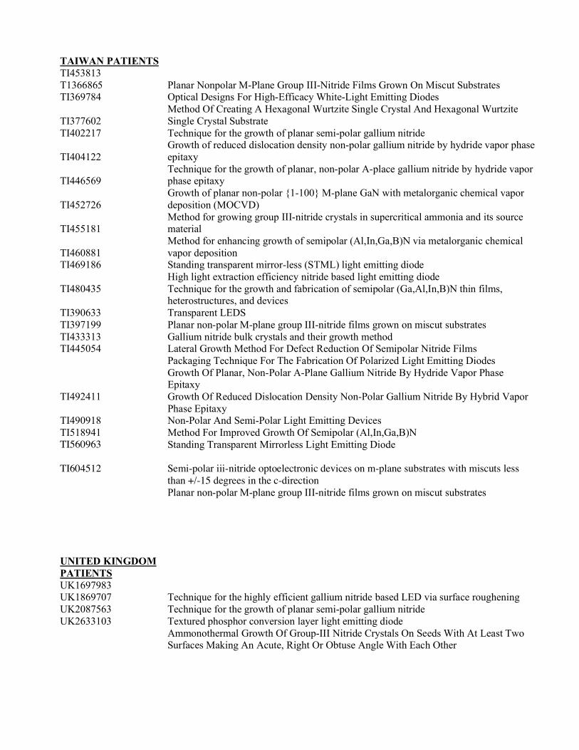
TAIWAN PATIENTS TI453813 T1366865 TI369784 TI377602 TI402217 TI404122 TI446569 TI452726 TI455181 TI460881 TI469186 TI480435 TI390633 TI397199 TI433313 TI445054 TI492411 TI490918 TI518941 TI560963 TI604512
Planar Nonpolar M-Plane Group III-Nitride Films Grown On Miscut Substrates Optical Designs For High-Efficacy White-Light Emitting Diodes Method Of Creating A Hexagonal Wurtzite Single Crystal And Hexagonal Wurtzite Single Crystal Substrate Technique for the growth of planar semi-polar gallium nitride Growth of reduced dislocation density non-polar gallium nitride by hydride vapor phase epitaxy Technique for the growth of planar, non-polar A-place gallium nitride by hydride vapor phase epitaxy Growth of planar non-polar {1-100} M-plane GaN with metalorganic chemical vapor deposition (MOCVD) Method for growing group III-nitride crystals in supercritical ammonia and its source material Method for enhancing growth of semipolar (Al,In,Ga,B)N via metalorganic chemical vapor deposition Standing transparent mirror-less (STML) light emitting diode High light extraction efficiency nitride based light emitting diode Technique for the growth and fabrication of semipolar (Ga,Al,In,B)N thin films, heterostructures, and devices Transparent LEDS Planar non-polar M-plane group III-nitride films grown on miscut substrates Gallium nitride bulk crystals and their growth method Lateral Growth Method For Defect Reduction Of Semipolar Nitride Films Packaging Technique For The Fabrication Of Polarized Light Emitting Diodes Growth Of Planar, Non-Polar A-Plane Gallium Nitride By Hydride Vapor Phase Epitaxy Growth Of Reduced Dislocation Density Non-Polar Gallium Nitride By Hybrid Vapor Phase Epitaxy Non-Polar And Semi-Polar Light Emitting Devices Method For Improved Growth Of Semipolar (Al,In,Ga,B)N Standing Transparent Mirrorless Light Emitting Diode Semi-polar iii-nitride optoelectronic devices on m-plane substrates with miscuts less than +/-15 degrees in the c-direction Planar non-polar M-plane group III-nitride films grown on miscut substrates
UNITED KINGDOM PATIENTS UK1697983 UK1869707 UK2087563 UK2633103
Technique for the highly efficient gallium nitride based LED via surface roughening Technique for the growth of planar semi-polar gallium nitride Textured phosphor conversion layer light emitting diode Ammonothermal Growth Of Group-III Nitride Crystals On Seeds With At Least Two Surfaces Making An Acute, Right Or Obtuse Angle With Each Other