Embed Size (px)
Citation preview

Serial RapidIO Gen2 Endpoint v4.1
LogiCORE IP Product Guide
Vivado Design Suite
PG007 June 7, 2017

Serial RapidIO Gen2 v4.1 www.xilinx.com 2PG007 June 7, 2017
Table of ContentsIP Facts
Chapter 1: OverviewSystem Overview . . . . . . . . . . . . . . . . . . . . . . . . . . . . . . . . . . . . . . . . . . . . . . . . . . . . . . . . . . . . . . . . . . 5Applications . . . . . . . . . . . . . . . . . . . . . . . . . . . . . . . . . . . . . . . . . . . . . . . . . . . . . . . . . . . . . . . . . . . . . . 7Unsupported Features. . . . . . . . . . . . . . . . . . . . . . . . . . . . . . . . . . . . . . . . . . . . . . . . . . . . . . . . . . . . . . 7Licensing . . . . . . . . . . . . . . . . . . . . . . . . . . . . . . . . . . . . . . . . . . . . . . . . . . . . . . . . . . . . . . . . . . . . . . . . . 7Recommended Design Experience . . . . . . . . . . . . . . . . . . . . . . . . . . . . . . . . . . . . . . . . . . . . . . . . . . . . 8
Chapter 2: Product SpecificationStandards Compliance . . . . . . . . . . . . . . . . . . . . . . . . . . . . . . . . . . . . . . . . . . . . . . . . . . . . . . . . . . . . . . 9Performance. . . . . . . . . . . . . . . . . . . . . . . . . . . . . . . . . . . . . . . . . . . . . . . . . . . . . . . . . . . . . . . . . . . . . 10Resource Utilization. . . . . . . . . . . . . . . . . . . . . . . . . . . . . . . . . . . . . . . . . . . . . . . . . . . . . . . . . . . . . . . 10Serial Transceiver Support. . . . . . . . . . . . . . . . . . . . . . . . . . . . . . . . . . . . . . . . . . . . . . . . . . . . . . . . . . 10Top-Level Wrapper . . . . . . . . . . . . . . . . . . . . . . . . . . . . . . . . . . . . . . . . . . . . . . . . . . . . . . . . . . . . . . . 11Port Descriptions . . . . . . . . . . . . . . . . . . . . . . . . . . . . . . . . . . . . . . . . . . . . . . . . . . . . . . . . . . . . . . . . . 11Register Space . . . . . . . . . . . . . . . . . . . . . . . . . . . . . . . . . . . . . . . . . . . . . . . . . . . . . . . . . . . . . . . . . . . 51
Chapter 3: Designing with the CoreGeneral Design Guidelines . . . . . . . . . . . . . . . . . . . . . . . . . . . . . . . . . . . . . . . . . . . . . . . . . . . . . . . . . 73Clocking. . . . . . . . . . . . . . . . . . . . . . . . . . . . . . . . . . . . . . . . . . . . . . . . . . . . . . . . . . . . . . . . . . . . . . . . . 91Resets . . . . . . . . . . . . . . . . . . . . . . . . . . . . . . . . . . . . . . . . . . . . . . . . . . . . . . . . . . . . . . . . . . . . . . . . . 100Shared Logic Related Port Descriptions . . . . . . . . . . . . . . . . . . . . . . . . . . . . . . . . . . . . . . . . . . . . . . 100Protocol Description . . . . . . . . . . . . . . . . . . . . . . . . . . . . . . . . . . . . . . . . . . . . . . . . . . . . . . . . . . . . . 102
Chapter 4: Design Flow StepsCustomizing and Generating the Core . . . . . . . . . . . . . . . . . . . . . . . . . . . . . . . . . . . . . . . . . . . . . . . 129Constraining the Core . . . . . . . . . . . . . . . . . . . . . . . . . . . . . . . . . . . . . . . . . . . . . . . . . . . . . . . . . . . . 149Simulation . . . . . . . . . . . . . . . . . . . . . . . . . . . . . . . . . . . . . . . . . . . . . . . . . . . . . . . . . . . . . . . . . . . . . 152Synthesis and Implementation . . . . . . . . . . . . . . . . . . . . . . . . . . . . . . . . . . . . . . . . . . . . . . . . . . . . . 152
Chapter 5: Detailed Example DesignOverview . . . . . . . . . . . . . . . . . . . . . . . . . . . . . . . . . . . . . . . . . . . . . . . . . . . . . . . . . . . . . . . . . . . . . . 153
Send Feedback

Serial RapidIO Gen2 v4.1 www.xilinx.com 3PG007 June 7, 2017
Generating the Core. . . . . . . . . . . . . . . . . . . . . . . . . . . . . . . . . . . . . . . . . . . . . . . . . . . . . . . . . . . . . . 153Directory and File Contents. . . . . . . . . . . . . . . . . . . . . . . . . . . . . . . . . . . . . . . . . . . . . . . . . . . . . . . . 154Example Design . . . . . . . . . . . . . . . . . . . . . . . . . . . . . . . . . . . . . . . . . . . . . . . . . . . . . . . . . . . . . . . . . 157Implementing the Example Design. . . . . . . . . . . . . . . . . . . . . . . . . . . . . . . . . . . . . . . . . . . . . . . . . . 162Simulating the Example Design. . . . . . . . . . . . . . . . . . . . . . . . . . . . . . . . . . . . . . . . . . . . . . . . . . . . . 162
Chapter 6: Test BenchDemonstration Test Bench . . . . . . . . . . . . . . . . . . . . . . . . . . . . . . . . . . . . . . . . . . . . . . . . . . . . . . . . 165
Appendix A: Packet and Control Symbol FormatsScope. . . . . . . . . . . . . . . . . . . . . . . . . . . . . . . . . . . . . . . . . . . . . . . . . . . . . . . . . . . . . . . . . . . . . . . . . . 167
Appendix B: Migrating and UpgradingMigrating to the Vivado Design Suite. . . . . . . . . . . . . . . . . . . . . . . . . . . . . . . . . . . . . . . . . . . . . . . . 170Upgrading in the Vivado Design Suite . . . . . . . . . . . . . . . . . . . . . . . . . . . . . . . . . . . . . . . . . . . . . . . 170
Appendix C: DebuggingFinding Help on Xilinx.com . . . . . . . . . . . . . . . . . . . . . . . . . . . . . . . . . . . . . . . . . . . . . . . . . . . . . . . . 178Debug Tools . . . . . . . . . . . . . . . . . . . . . . . . . . . . . . . . . . . . . . . . . . . . . . . . . . . . . . . . . . . . . . . . . . . . 180Waveform Analysis and Debug . . . . . . . . . . . . . . . . . . . . . . . . . . . . . . . . . . . . . . . . . . . . . . . . . . . . . 180Hardware Debug . . . . . . . . . . . . . . . . . . . . . . . . . . . . . . . . . . . . . . . . . . . . . . . . . . . . . . . . . . . . . . . . 189
Appendix D: Additional Resources and Legal NoticesXilinx Resources . . . . . . . . . . . . . . . . . . . . . . . . . . . . . . . . . . . . . . . . . . . . . . . . . . . . . . . . . . . . . . . . . 195References . . . . . . . . . . . . . . . . . . . . . . . . . . . . . . . . . . . . . . . . . . . . . . . . . . . . . . . . . . . . . . . . . . . . . 195Revision History . . . . . . . . . . . . . . . . . . . . . . . . . . . . . . . . . . . . . . . . . . . . . . . . . . . . . . . . . . . . . . . . . 196Please Read: Important Legal Notices . . . . . . . . . . . . . . . . . . . . . . . . . . . . . . . . . . . . . . . . . . . . . . . 197
Send Feedback
Serial RapidIO Gen2 v4.1 www.xilinx.com 4PG007 June 7, 2017 Product Specification
IntroductionThe LogiCORE™ IP Serial RapidIO Gen2 Endpoint Solution (SRIO Gen2 Endpoint) comprises a highly flexible and optimized Serial RapidIO Gen2 Physical Layer and a Serial RapidIO Gen2 Logical (I/O) and Transport Layer. This IP solution is provided in netlist form with supporting example design code. The SRIO Gen2 Endpoint supports 1x, 2x, and 4x lane widths. It comes with a configurable buffer design, reference clock module, reset module, and configuration fabric reference design. The SRIO Gen2 Endpoint uses AXI4-Stream interfaces for high-throughput data transfer and AXI4-Lite interfaces for the configuration (maintenance) interfaces.
Features• Designed to RapidIO Interconnect
Specification rev. 2.2
• Supports 1x, 2x and 4x operation with the ability to train down to 1x from 2x or 4x
• Supports per-lane speeds of 1.25, 2.5, 3.125, 5.0, and 6.25 Gbaud
Logical Layer • Concurrent Initiator and Target operations
• Doorbell and Message support
• Dedicated port for maintenance transactions
• Simple handshaking mechanism to control data flow using standard AXI4-Lite and AXI4-Stream interfaces
• Programmable source ID on all outgoing packets
• Optional large system support for 16-bit device IDs
Buffer • Independently configurable TX and RX Buffer
depths of 8, 16, or 32 packets
• Support for independent clocks
• Optional TX Flow Control support
Physical Layer • Configurable IDLE1/IDLE2 sequence
support
• Supports critical request flow
• Support for multicast events
IP Facts
LogiCORE IP Facts Table
Core Specifics
Supported Device Family (1)
1. For a complete list of supported devices, see the Vivado IP catalog.
UltraScale+™ Families,UltraScale™ Architecture, Zynq®-7000,
Virtex®-7, Kintex®-7, Artix®-7
Supported User Interfaces AXI4-Stream, AXI4-Lite
Resources Performance and Resource Utilization web page
Provided with CoreDesign Files Encrypted RTL
Example DesignConfiguration Fabric Design
with Verilog Source
Test Bench Verilog
Constraints File XDC
Simulation Model Encrypted Verilog
Supported S/W Driver N/A
Tested Design Flows (2)
2. For the supported versions of the tools, see theXilinx Design Tools: Release Notes Guide.
Design Entry Vivado® Design Suite
Simulation (3)
3. Requires a Verilog LRM-IEEE 1364-2005 encryption-compliant simulator.
For the supported simulators, see the XilinxDesign Tools: Release Notes Guide
Synthesis Vivado synthesis
SupportProvided by Xilinx at the Xilinx Support web page
Send Feedback
Serial RapidIO Gen2 v4.1 www.xilinx.com 5PG007 June 7, 2017
Chapter 1
OverviewThe RapidIO Interconnect Architecture, designed to be compatible with the most popular integrated communications processors, host processors, and networking digital signal processors, is a high-performance, packet-switched, interconnect technology. It addresses the need of the high-performance embedded industry for reliability, increased bandwidth, and faster bus speeds in an intra-system interconnect.
The RapidIO standard is defined in three layers: logical, transport and physical. The logical layer defines the overall protocol and packet formats. This is the information necessary for endpoints to initiate and complete a transaction. The transport layer provides the route information necessary for a packet to move from endpoint to endpoint. The physical layer describes the device-level interface specifics such as packet transport mechanisms, flow control, electrical characteristics, and low-level error management. This partitioning provides the flexibility to add new transaction types to the logical specification without requiring modification to the transport or physical layer specifications.
• For more information about the RapidIO core, see www.xilinx.com/rapidio
• For more information about the RapidIO standards and specifications, see www.rapidio.org
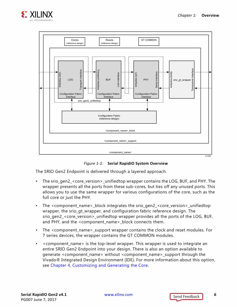
System OverviewThe SRIO Gen2 Endpoint is comprised of the following:
• A Serial RapidIO Gen2 top-level wrapper (srio_gen2_<core_version>_unifiedtop) containing:
° Serial RapidIO Gen2 Physical Layer (PHY)
° Serial RapidIO Gen2 Logical (I/O) and Transport Layer (LOG)
° Serial RapidIO Gen2 Buffer Design (BUF)
• Reference design for clocking, resets, and configuration accesses
The SRIO Gen2 Endpoint is shown in Figure 1-1.
Send Feedback
Serial RapidIO Gen2 v4.1 www.xilinx.com 6PG007 June 7, 2017
Chapter 1: Overview
The SRIO Gen2 Endpoint is delivered through a layered approach.
• The srio_gen2_<core_version>_unifiedtop wrapper contains the LOG, BUF, and PHY. The wrapper presents all the ports from these sub-cores, but ties off any unused ports. This allows you to use the same wrapper for various configurations of the core, such as the full core or just the PHY.
• The <component_name>_block integrates the srio_gen2_<core_version>_unifiedtop wrapper, the srio_gt_wrapper, and configuration fabric reference design. The srio_gen2_<core_version>_unifiedtop wrapper provides all the ports of the LOG, BUF, and PHY, and the <component_name>_block connects them.
• The <component_name>_support wrapper contains the clock and reset modules. For 7 series devices, the wrapper contains the GT COMMON modules.
• <component_name> is the top-level wrapper. This wrapper is used to integrate an entire SRIO Gen2 Endpoint into your design. There is also an option available to generate <component_name> without <component_name>_support through the Vivado® Integrated Design Environment (IDE). For more information about this option, see Chapter 4, Customizing and Generating the Core.
X-Ref Target - Figure 1-1
Figure 1-1: Serial RapidIO System Overview
( )
srio_gt_wrapper
Tran
scei
ver I
nter
faceS
erial Interface
Configuration FabricInterface
PHY
Link Interface
Ser
ial I
nter
face
Configuration FabricInterface
BUF
Transport Interface Link
Inte
rface
Configuration FabricInterface
LOG
User Interface
Tran
spor
t Int
erfa
ce
Configuration Fabric(reference design)
Clocks(reference design)
Resets(reference design)
GT COMMON
srio_gen2_unifiedtop
<component_name>
<component_name>_support
<component_name>_block
X12697
Send Feedback
Serial RapidIO Gen2 v4.1 www.xilinx.com 7PG007 June 7, 2017
Chapter 1: Overview
Although not shown in Figure 1-1, the srio_example_top wrapper includes all the components described previously in addition to an example design. This is used for testing and demonstration purposes, both in simulation and hardware.
ApplicationsThe SRIO Gen2 Endpoint is well suited for control and data operations in communication and embedded systems requiring high-speed I/O with low latency. Typical applications include:
• Wireless Base Stations as interconnect on Channel Cards or Radio Equipment controller
• DSP farms for image and signal processing which is ideal for multi-processor communication interconnect
• Scientific, military, and industrial equipment
• High-availability enterprise storage as reliable, low latency, and high bandwidth memory interface
• Edge Networking for multimedia data compression
Unsupported FeaturesThe following feature is not supported:
• Train down to lane-R (redundant lane). The redundant lane is lane 1 in a x2 configuration, and is lane 2 in a x4 configuration.
Licensing
License CheckersIf the IP requires a license key, the key must be verified. The Vivado® design tools have several license checkpoints for gating licensed IP through the flow. If the license check succeeds, the IP can continue generation. Otherwise, generation halts with error. License checkpoints are enforced by the following Vivado design tools:
• Vivado synthesis
• Vivado implementation
• write_bitstream (Tcl command)
Send Feedback
Serial RapidIO Gen2 v4.1 www.xilinx.com 8PG007 June 7, 2017
Chapter 1: Overview
IMPORTANT: IP license level is ignored at checkpoints. The test confirms a valid license exists. It does not check IP license level.
License TypeThis Xilinx LogiCORE™ IP module is provided under the terms of the Xilinx Core License Agreement. The module is shipped as part of the Vivado Design Suite. For full access to all core features in simulation and in hardware, you must purchase a license for the core. Contact your local Xilinx sales representative for information about pricing and availability.
For more information, please visit the Serial RapidIO Gen2 product page.
Information about other Xilinx LogiCORE IP modules is available at the Xilinx Intellectual Property page. For information on pricing and availability of other Xilinx LogiCORE IP modules and tools, contact your local Xilinx sales representative.
Recommended Design ExperienceAlthough the SRIO Gen2 Endpoint is fully verified, the challenge associated with implementing a complete design varies depending on the configuration and functionality of the application.
RECOMMENDED: For best results, previous experience building high performance, pipelined FPGA designs using Xilinx implementation software and a Xilinx design constraints (XDC) file is recommended. Design flow training about XDC files can been found at www.xilinx.com/training/fpga/
essentials-of-fpga-design.htm.
Contact your local Xilinx representative for a closer review and estimation for your specific requirements.
Send Feedback

Serial RapidIO Gen2 v4.1 www.xilinx.com 9PG007 June 7, 2017
Chapter 2
Product SpecificationThe SRIO Gen2 Endpoint is presented as three sub-cores (provided through the srio_gen2_<core_version>_unifiedtop wrapper) combined into a single solution using the <component_name> module. The wrapper provides a high-level, low maintenance interface for most use models while allowing control of sub-components where necessary.
This chapter gives a basic, functional overview for each sub-core and interface including signal lists and register definitions. Not all the signals listed in the following sections come out of the <component_name>.
Standards ComplianceThe Serial RapidIO Gen2 Physical Layer (PHY), Serial RapidIO Gen2 Logical Layer (LOG), and Serial RapidIO Gen2 Buffer (BUF) are designed according the RapidIO Interconnect Specification rev. 2.2 (RapidIO Specification) [Ref 13]. Although working knowledge of the RapidIO Specification is not required to use the SRIO Gen2 Endpoint, it might be necessary to reference the specifications for details outside of the scope of this guide. This guide references portions of the RapidIO Specification when necessary.
The following list of the chapters of the RapidIO Interconnect Specification rev 2.2 specification directly relate to the SRIO Gen2 Endpoint:
• Part 1: Input/Output System Logical – Specifies functionality of the Serial RapidIO Gen2 Logical (I/O) and Transport Layer.
• Part 2: Message Passing Logical – Specifies functionality of the Serial RapidIO Gen2 Logical (I/O) and Transport Layer when Doorbell and Message parsing is enabled.
• Part 3: Common Transport – Specifies functionality of the Serial RapidIO Gen2 Logical (I/O) and Transport Layer.
• Part 6: Serial Physical Layer – Specifies functionality of the Serial RapidIO Gen2 Physical Layer and the Serial RapidIO Gen2 Buffer.
Send Feedback
Serial RapidIO Gen2 v4.1 www.xilinx.com 10PG007 June 7, 2017
Chapter 2: Product Specification
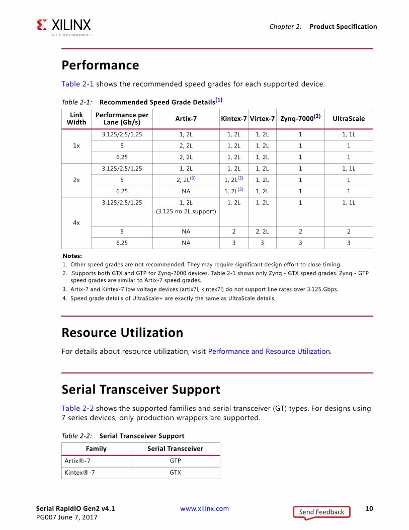
PerformanceTable 2-1 shows the recommended speed grades for each supported device.
Resource UtilizationFor details about resource utilization, visit Performance and Resource Utilization.
Serial Transceiver SupportTable 2-2 shows the supported families and serial transceiver (GT) types. For designs using 7 series devices, only production wrappers are supported.
Table 2-1: Recommended Speed Grade Details(1)
Link Width
Performance per Lane (Gb/s) Artix-7 Kintex-7 Virtex-7 Zynq-7000(2) UltraScale
1x
3.125/2.5/1.25 1, 2L 1, 2L 1, 2L 1 1, 1L
5 2, 2L 1, 2L 1, 2L 1 1
6.25 2, 2L 1, 2L 1, 2L 1 1
2x
3.125/2.5/1.25 1, 2L 1, 2L 1, 2L 1 1, 1L
5 2, 2L(3) 1, 2L(3) 1, 2L 1 1
6.25 NA 1, 2L(3) 1, 2L 1 1
4x
3.125/2.5/1.25 1, 2L(3.125 no 2L support)
1, 2L 1, 2L 1 1, 1L
5 NA 2 2, 2L 2 2
6.25 NA 3 3 3 3
Notes: 1. Other speed grades are not recommended. They may require significant design effort to close timing.2. .Supports both GTX and GTP for Zynq-7000 devices. Table 2-1 shows only Zynq - GTX speed grades. Zynq - GTP
speed grades are similar to Artix-7 speed grades.3. Artix-7 and Kintex-7 low voltage devices (artix7l, kintex7l) do not support line rates over 3.125 Gbps.4. Speed grade details of UltraScale+ are exactly the same as UltraScale details.
Table 2-2: Serial Transceiver Support
Family Serial Transceiver
Artix®-7 GTP
Kintex®-7 GTX
Send Feedback
Serial RapidIO Gen2 v4.1 www.xilinx.com 11PG007 June 7, 2017
Chapter 2: Product Specification
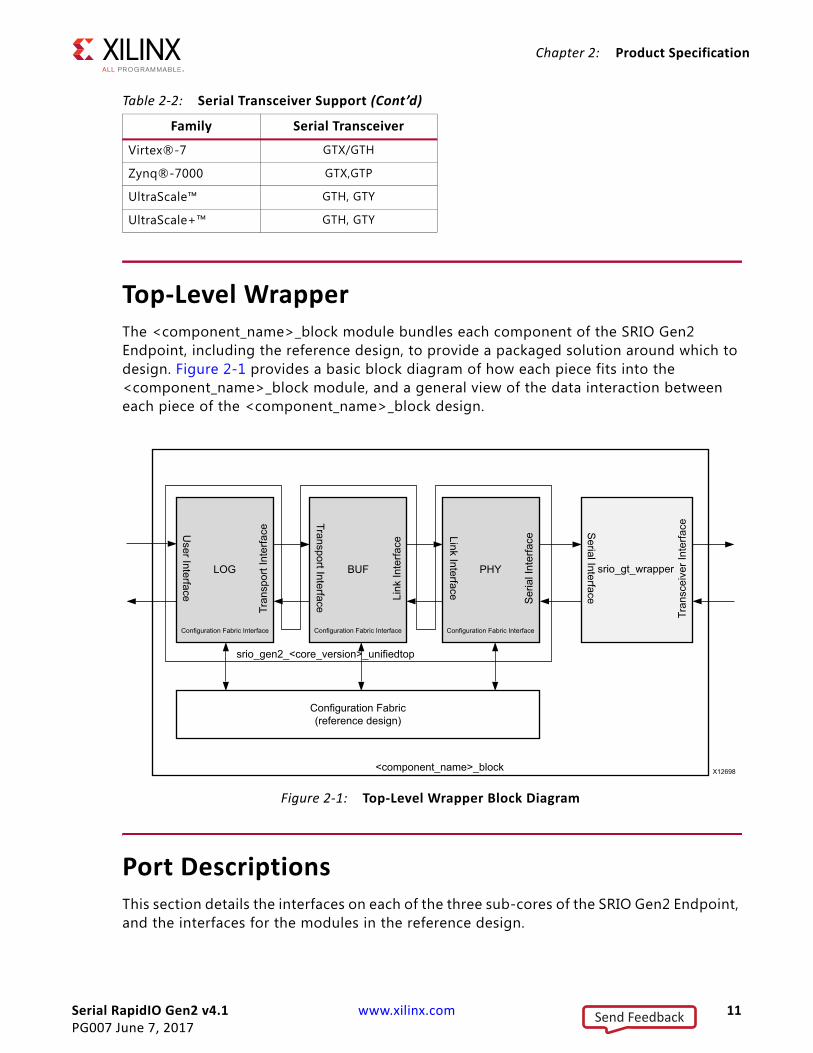
Top-Level WrapperThe <component_name>_block module bundles each component of the SRIO Gen2 Endpoint, including the reference design, to provide a packaged solution around which to design. Figure 2-1 provides a basic block diagram of how each piece fits into the <component_name>_block module, and a general view of the data interaction between each piece of the <component_name>_block design.
Port DescriptionsThis section details the interfaces on each of the three sub-cores of the SRIO Gen2 Endpoint, and the interfaces for the modules in the reference design.
Virtex®-7 GTX/GTH
Zynq®-7000 GTX,GTP
UltraScale™ GTH, GTY
UltraScale+™ GTH, GTY
X-Ref Target - Figure 2-1
Figure 2-1: Top-Level Wrapper Block Diagram
Table 2-2: Serial Transceiver Support (Cont’d)
Family Serial Transceiver
<component_name>_block
LOG BUF PHY
Configuration Fabric(reference design)
srio_gt_wrapper
User Interface
Transport Interface
Link InterfaceLink
Inte
rface
Ser
ial I
nter
face
Tran
spor
t Int
erfa
ce
Configuration Fabric Interface Configuration Fabric Interface Configuration Fabric Interface
Tran
scei
ver I
nter
faceS
erial Interface
srio_gen2_<core_version>_unifiedtop
X12698
Send Feedback
Serial RapidIO Gen2 v4.1 www.xilinx.com 12PG007 June 7, 2017
Chapter 2: Product Specification
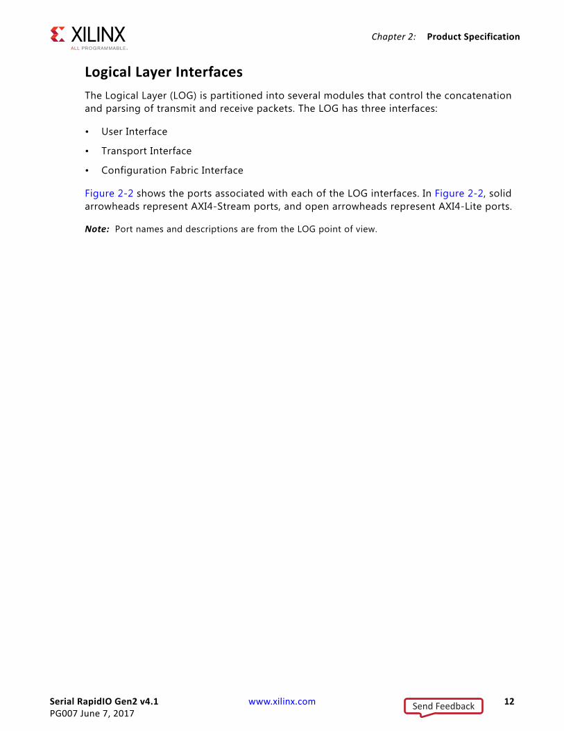
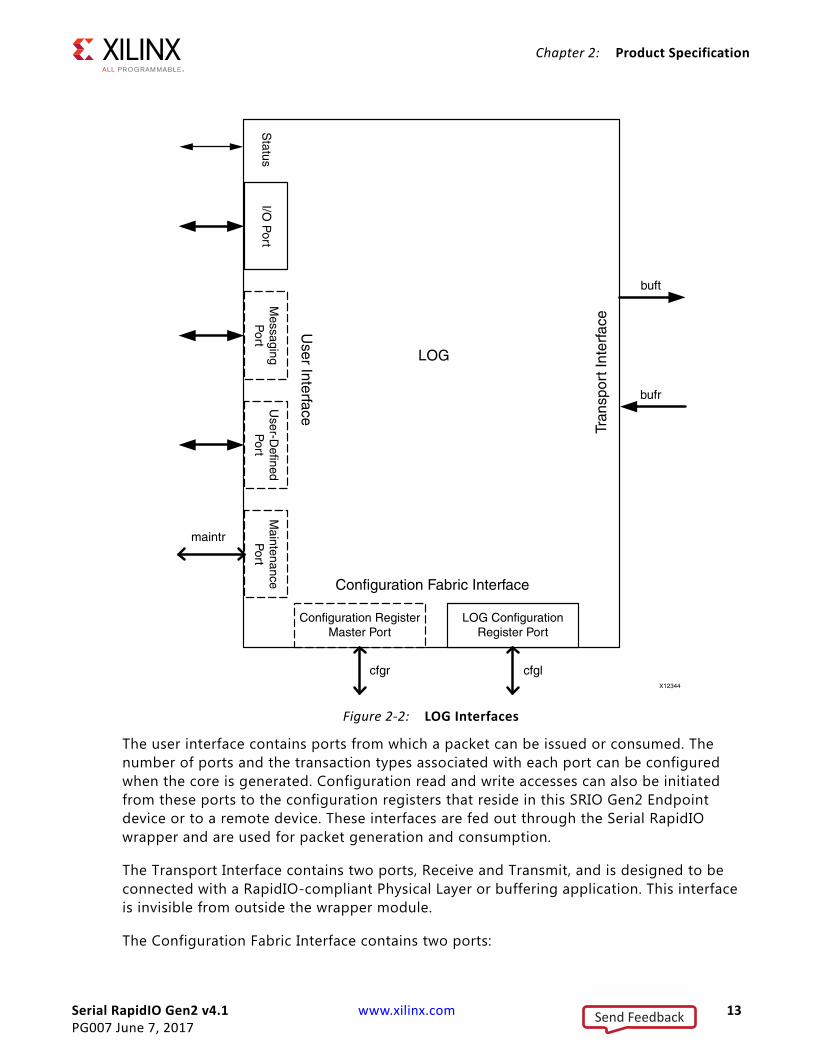
Logical Layer InterfacesThe Logical Layer (LOG) is partitioned into several modules that control the concatenation and parsing of transmit and receive packets. The LOG has three interfaces:
• User Interface
• Transport Interface
• Configuration Fabric Interface
Figure 2-2 shows the ports associated with each of the LOG interfaces. In Figure 2-2, solid arrowheads represent AXI4-Stream ports, and open arrowheads represent AXI4-Lite ports.
Note: Port names and descriptions are from the LOG point of view.
Send Feedback
Serial RapidIO Gen2 v4.1 www.xilinx.com 13PG007 June 7, 2017
Chapter 2: Product Specification
The user interface contains ports from which a packet can be issued or consumed. The number of ports and the transaction types associated with each port can be configured when the core is generated. Configuration read and write accesses can also be initiated from these ports to the configuration registers that reside in this SRIO Gen2 Endpoint device or to a remote device. These interfaces are fed out through the Serial RapidIO wrapper and are used for packet generation and consumption.
The Transport Interface contains two ports, Receive and Transmit, and is designed to be connected with a RapidIO-compliant Physical Layer or buffering application. This interface is invisible from outside the wrapper module.
The Configuration Fabric Interface contains two ports:
X-Ref Target - Figure 2-2
Figure 2-2: LOG Interfaces
Send Feedback
Serial RapidIO Gen2 v4.1 www.xilinx.com 14PG007 June 7, 2017
Chapter 2: Product Specification
• Configuration Master port, which issues reads and writes to the local configuration space through the Configuration Fabric.
• LOG Configuration Register port, which is a slave interface for reads and writes to any configuration registers that are defined as part of the Logical or Transport Layers.
The Configuration Fabric decodes the address of reads or writes from the Configuration Bus Master and passes them to the Configuration Register ports of the LOG, PHY and BUF. This interaction is kept completely within the <component_name>_block module.
Clock and Reset Interface
Table 2-3 lists the signals associated with the clock and resets for the LOG layer at <component_name>_block.
Table 2-3: LOG Clock and Reset Interface Signal List
Signal Direction Description
log_lcl_log_clk Output
Clock for the LOG. In example design, log_clk depends on line rate and link width (a core trained down from Nx to 1x still uses the Nx clock rate). See Clocking in Chapter 3 for more information.
Note: This signal is the same as log_clk, which is the name used in other areas of this document.
log_rst Input Reset for LOG. Must deassert synchronously to log_clk. See Resets in Chapter 3.
log_lcl_cfg_clk Input
Configuration Register Interface clock. If the AXI4-Lite Maintenance Port and the Configuration Fabric reference design are in use, this must be equivalent to log_clk. Otherwise, this clock is independent of log_clk.
Note: This signal is the same as cfg_clk, which is the name used in other areas of this document.
log_lcl_cfg_rst Input
Configuration Register Interface reset. Clears LOG registers to default values. Must deassert synchronously to cfg_clk.
Note: This signal is the same as cfg_rst, which is the name used in other areas of this document.
Send Feedback

Serial RapidIO Gen2 v4.1 www.xilinx.com 15PG007 June 7, 2017
Chapter 2: Product Specification
User Interfaces
The user interface contains a set of I/O ports and the following optional ports:
• Messaging Port
• Maintenance Port
• User-Defined Port
These interfaces are available from the <component_name>_block level. Each transaction type is assigned to a particular port. Typically, any supported I/O transactions such as NWRITEs, NWRITE_Rs, SWRITEs, NREADs, and RESPONSEs (not including MAINTENANCE responses) are transmitted or received on the I/O port. MESSAGE transactions (if supported) can be assigned to either the Messaging port or the I/O port. DOORBELL transactions use the I/O port regardless of whether the Messaging port is present. If the Maintenance port is enabled, all Maintenance packets are expected on the Maintenance port. If a transaction is user-defined, an unsupported type, or does not have an assigned port, it uses the User-Defined port (when the User-Defined port is disabled, received packets that do not correspond to another port are dropped).
I/O Port
The I/O port can be configured in one of two styles: Condensed I/O or Initiator/Target. The signals available depend on the style selected during core generation.
The I/O port is built from AXI4-Stream channels. Two packet formats are available:
• HELLO
• SRIO Stream
IMPORTANT: All channels in the I/O port must use the same packet format, which is selected when the core is generated. See Chapter 3, Designing with the Core for more information on port usage.
Condensed I/O
The Condensed I/O port style reduces the number of channels used to transmit and receive I/O packets. There is one AXI4-Stream channel used to transmit all packet types associated with the I/O port (iotx). Similarly, there is one channel used for all received I/O port packets (iorx). Figure 2-3 shows the Condensed I/O port.
Note: Port names and descriptions are from the LOG point of view.
Send Feedback

Serial RapidIO Gen2 v4.1 www.xilinx.com 16PG007 June 7, 2017
Chapter 2: Product Specification
Table 2-4 lists the signals associated with the Condensed I/O port. The s_axis_iotx* signals are associated with the CONDENSED_IO_TX interface, and the m_axis_iorx* signals are associated with the CONDENSED_IO_RX interface at the <component_name> level.
X-Ref Target - Figure 2-3
Figure 2-3: Condensed I/O Port
Table 2-4: Condensed I/O Port Signal List
Signal Direction Description
s_axis_iotx_tvalid Input Indicates that the information on the channel is valid.
s_axis_iotx_tready Output Handshaking signal. Indicates that the data from the source is accepted (if valid).
s_axis_iotx_tdata[63:0] Input Packet header and data.
s_axis_iotx_tkeep[7:0] Input
Byte qualifier that indicates whether the content of the associated byte of data is valid. If port is configured to use HELLO format, this must be tied to 8’hFF. For ports configured to use SRIO Stream format, this input should be set to 8'hFF except when tlast is asserted.Bit 7 corresponds to the most significant byte of data (tdata[63:56]), and bit 0 corresponds to the least significant byte (tdata[7:0]).
s_axis_iotx_tlast Input Indicates the last beat of a packet.
Send Feedback

Serial RapidIO Gen2 v4.1 www.xilinx.com 17PG007 June 7, 2017
Chapter 2: Product Specification
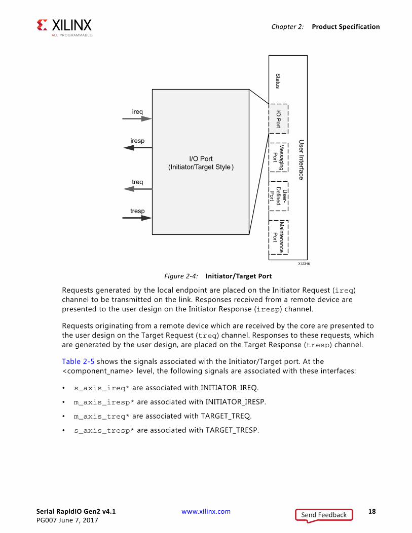
Initiator/Target
The Initiator/Target port style allows separation of transactions intended for remote devices (placed on Initiator port) from transactions targeting the local endpoint (placed on Target port).
As shown in Figure 2-4, there are four AXI4-Stream channels for I/O transactions when using the Initiator/Target port style. In Figure 2-4, request channels are shown in black and response channels in gray.
Note: Port names and descriptions are from the LOG point of view.
s_axis_iotx_tuser[31:0] Input
HELLO Format: Valid on the first beat of a packet, this signal consists of the Source ID (31:16) and Destination ID (15:0) for the packet. If using 8-bit Device IDs, the most significant byte of each ID should be padded with 0s. The Source ID portion of the signal is tied to the deviceid signal.SRIO Stream Format: In this format, tuser is only 8 bits wide. Bit 1 is used to set the Critical Request Flow (CRF) flag for the packet, and should be tied to zero if CRF support is disabled. All other bits are reserved.On subsequent beats within a packet, this field is reserved.
m_axis_iorx_tvalid Output Indicates that the information on the channel is valid.
m_axis_iorx_tready Input Handshaking signal. Indicates that the data from the source is accepted (if valid).
m_axis_iorx_tdata[63:0] Output Packet header and data.
m_axis_iorx_tkeep[7:0] Output
Byte qualifier that indicates whether the content of the associated byte of data is valid. If port is configured to use HELLO format, this is tied to 8’hFF. For ports configured to use SRIO Stream format, this output is set to 8'hFF except when tlast is asserted.Bit 7 corresponds to the most significant byte of data (tdata[63:56]) and bit 0 corresponds to the least significant byte (tdata[7:0]).
m_axis_iorx_tlast Output Indicates the last beat of a packet.
m_axis_iorx_tuser[31:0] Output
HELLO Format: Valid on the first beat of a packet, this signal consists of the Source ID (31:16) and Destination ID (15:0) for the packet. If using 8-bit Device IDs, the most significant byte of each ID is padded with 0s.SRIO Stream Format: In this format, tuser is only 8 bits wide. Bit 1 is set if the Critical Request Flow (CRF) flag for the packet was set. All other bits are reserved.On subsequent beats within a packet, this field is reserved.
Table 2-4: Condensed I/O Port Signal List (Cont’d)
Signal Direction Description
Send Feedback
Serial RapidIO Gen2 v4.1 www.xilinx.com 18PG007 June 7, 2017
Chapter 2: Product Specification
Requests generated by the local endpoint are placed on the Initiator Request (ireq) channel to be transmitted on the link. Responses received from a remote device are presented to the user design on the Initiator Response (iresp) channel.
Requests originating from a remote device which are received by the core are presented to the user design on the Target Request (treq) channel. Responses to these requests, which are generated by the user design, are placed on the Target Response (tresp) channel.
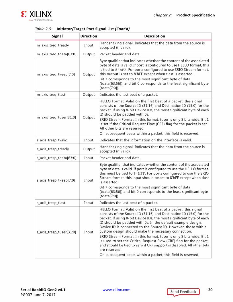
Table 2-5 shows the signals associated with the Initiator/Target port. At the <component_name> level, the following signals are associated with these interfaces:
• s_axis_ireq* are associated with INITIATOR_IREQ.
• m_axis_iresp* are associated with INITIATOR_IRESP.
• m_axis_treq* are associated with TARGET_TREQ.
• s_axis_tresp* are associated with TARGET_TRESP.
X-Ref Target - Figure 2-4
Figure 2-4: Initiator/Target Port
User Interface
I/O P
ortM
essaging P
ortM
aintenance P
ort
User-
Defined P
ort
I/O Port(Initiator/Target Style)
ireq
iresp
treq
tresp
Status
Send Feedback
Serial RapidIO Gen2 v4.1 www.xilinx.com 19PG007 June 7, 2017
Chapter 2: Product Specification
Table 2-5: Initiator/Target Port Signal List
Signal Direction Description
s_axis_ireq_tvalid Input Indicates that the information on the interface is valid.
s_axis_ireq_tready Output Handshaking signal. Indicates that the data from the source is accepted (if valid).
s_axis_ireq_tdata[63:0] Input Packet header and data.
s_axis_ireq_tkeep[7:0] Input
Byte qualifier that indicates whether the content of the associated byte of data is valid. If port is configured to use the HELLO format, this must be tied to 8’hFF. For ports configured to use the SRIO Stream format, this input should be set to 8'hFF except when tlast is asserted.Bit 7 corresponds to the most significant byte of data (tdata[63:56]), and bit 0 corresponds to the least significant byte (tdata[7:0]).
s_axis_ireq_tlast Input Indicates the last beat of a packet.
s_axis_ireq_tuser[31:0] Input
HELLO Format: Valid on the first beat of a packet, this signal consists of the Source ID (31:16) and Destination ID (15:0) for the packet. If using 8-bit Device IDs, the most significant byte of each ID should be padded with 0s. In the default example design, Device ID is connected to the Source ID. However, those with a custom design should make the necessary connection. SRIO Stream Format: In this format, tuser is only 8 bits wide. Bit 1 is used to set the Critical Request Flow (CRF) flag for the packet, and should be tied to zero if CRF support is disabled. All other bits are reserved.On subsequent beats within a packet, this field is reserved.
m_axis_iresp_tvalid Output Indicates that the information on the interface is valid.
m_axis_iresp_tready Input Handshaking signal. Indicates that the data from the source is accepted (if valid).
m_axis_iresp_tdata[63:0] Output Packet header and data.
m_axis_iresp_tkeep[7:0] Output
Byte qualifier that indicates whether the content of the associated byte of data is valid. If port is configured to use HELLO format, this is tied to 8’hFF. For ports configured to use SRIO Stream format, this output is set to 8'hFF except when tlast is asserted.Bit 7 corresponds to the most significant byte of data (tdata[63:56]) and bit 0 corresponds to the least significant byte (tdata[7:0]).
m_axis_iresp_tlast Output Indicates the last beat of a packet.
m_axis_iresp_tuser[31:0] Output
HELLO Format: Valid on the first beat of a packet, this signal consists of the Source ID (31:16) and Destination ID (15:0) for the packet. If using 8-bit Device IDs, the most significant byte of each ID should be padded with 0s.SRIO Stream Format: In this format, tuser is only 8 bits wide. Bit 1 is set if the Critical Request Flow (CRF) flag for the packet was set. All other bits are reserved.On subsequent beats within a packet, this field is reserved.
m_axis_treq_tvalid Output Indicates that information on the interface is valid.
Send Feedback
Serial RapidIO Gen2 v4.1 www.xilinx.com 20PG007 June 7, 2017
Chapter 2: Product Specification
m_axis_treq_tready Input Handshaking signal. Indicates that the data from the source is accepted (if valid).
m_axis_treq_tdata[63:0] Output Packet header and data.
m_axis_treq_tkeep[7:0] Output
Byte qualifier that indicates whether the content of the associated byte of data is valid. If port is configured to use HELLO format, this is tied to 8’hFF. For ports configured to use SRIO Stream format, this output is set to 8'hFF except when tlast is asserted.Bit 7 corresponds to the most significant byte of data (tdata[63:56]), and bit 0 corresponds to the least significant byte (tdata[7:0]).
m_axis_treq_tlast Output Indicates the last beat of a packet.
m_axis_treq_tuser[31:0] Output
HELLO Format: Valid on the first beat of a packet, this signal consists of the Source ID (31:16) and Destination ID (15:0) for the packet. If using 8-bit Device IDs, the most significant byte of each ID should be padded with 0s.SRIO Stream Format: In this format, tuser is only 8 bits wide. Bit 1 is set if the Critical Request Flow (CRF) flag for the packet is set. All other bits are reserved.On subsequent beats within a packet, this field is reserved.
s_axis_tresp_tvalid Input Indicates that the information on the interface is valid.
s_axis_tresp_tready Output Handshaking signal. Indicates that the data from the source is accepted (if valid).
s_axis_tresp_tdata[63:0] Input Packet header and data.
s_axis_tresp_tkeep[7:0] Input
Byte qualifier that indicates whether the content of the associated byte of data is valid. If port is configured to use the HELLO format, this must be tied to 8’hFF. For ports configured to use the SRIO Stream format, this input should be set to 8'hFF except when tlast is asserted.Bit 7 corresponds to the most significant byte of data (tdata[63:56]) and bit 0 corresponds to the least significant byte (tdata[7:0]).
s_axis_tresp_tlast Input Indicates the last beat of a packet.
s_axis_tresp_tuser[31:0] Input
HELLO Format: Valid on the first beat of a packet, this signal consists of the Source ID (31:16) and Destination ID (15:0) for the packet. If using 8-bit Device IDs, the most significant byte of each ID should be padded with 0s. In the default example design, Device ID is connected to the Source ID. However, those with a custom design should make the necessary connection.SRIO Stream Format: In this format, tuser is only 8 bits wide. Bit 1 is used to set the Critical Request Flow (CRF) flag for the packet, and should be tied to zero if CRF support is disabled. All other bits are reserved.On subsequent beats within a packet, this field is reserved.
Table 2-5: Initiator/Target Port Signal List (Cont’d)
Signal Direction Description
Send Feedback
Serial RapidIO Gen2 v4.1 www.xilinx.com 21PG007 June 7, 2017
Chapter 2: Product Specification
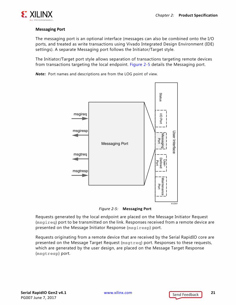
Messaging Port
The messaging port is an optional interface (messages can also be combined onto the I/O ports, and treated as write transactions using Vivado Integrated Design Environment (IDE) settings). A separate Messaging port follows the Initiator/Target style.
The Initiator/Target port style allows separation of transactions targeting remote devices from transactions targeting the local endpoint. Figure 2-5 details the Messaging port.
Note: Port names and descriptions are from the LOG point of view.
Requests generated by the local endpoint are placed on the Message Initiator Request (msgireq) port to be transmitted on the link. Responses received from a remote device are presented on the Message Initiator Response (msgiresp) port.
Requests originating from a remote device that are received by the Serial RapidIO core are presented on the Message Target Request (msgtreq) port. Responses to these requests, which are generated by the user design, are placed on the Message Target Response (msgtresp) port.
X-Ref Target - Figure 2-5
Figure 2-5: Messaging Port
Send Feedback
Serial RapidIO Gen2 v4.1 www.xilinx.com 22PG007 June 7, 2017
Chapter 2: Product Specification
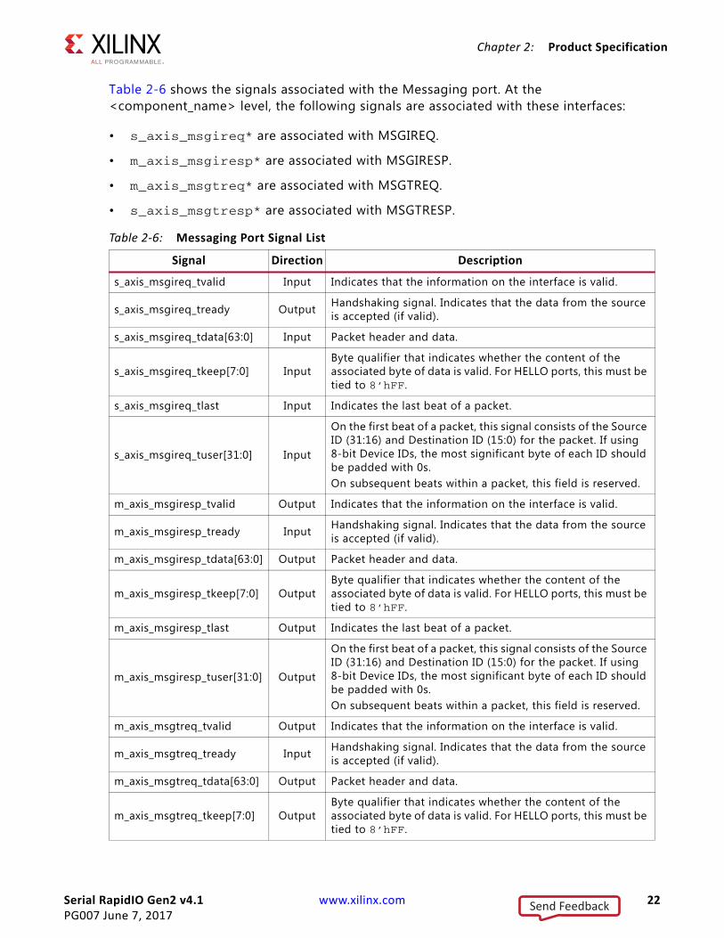
Table 2-6 shows the signals associated with the Messaging port. At the <component_name> level, the following signals are associated with these interfaces:
• s_axis_msgireq* are associated with MSGIREQ.
• m_axis_msgiresp* are associated with MSGIRESP.
• m_axis_msgtreq* are associated with MSGTREQ.
• s_axis_msgtresp* are associated with MSGTRESP.
Table 2-6: Messaging Port Signal List
Signal Direction Description
s_axis_msgireq_tvalid Input Indicates that the information on the interface is valid.
s_axis_msgireq_tready Output Handshaking signal. Indicates that the data from the source is accepted (if valid).
s_axis_msgireq_tdata[63:0] Input Packet header and data.
s_axis_msgireq_tkeep[7:0] InputByte qualifier that indicates whether the content of the associated byte of data is valid. For HELLO ports, this must be tied to 8’hFF.
s_axis_msgireq_tlast Input Indicates the last beat of a packet.
s_axis_msgireq_tuser[31:0] Input
On the first beat of a packet, this signal consists of the Source ID (31:16) and Destination ID (15:0) for the packet. If using 8-bit Device IDs, the most significant byte of each ID should be padded with 0s.On subsequent beats within a packet, this field is reserved.
m_axis_msgiresp_tvalid Output Indicates that the information on the interface is valid.
m_axis_msgiresp_tready Input Handshaking signal. Indicates that the data from the source is accepted (if valid).
m_axis_msgiresp_tdata[63:0] Output Packet header and data.
m_axis_msgiresp_tkeep[7:0] OutputByte qualifier that indicates whether the content of the associated byte of data is valid. For HELLO ports, this must be tied to 8’hFF.
m_axis_msgiresp_tlast Output Indicates the last beat of a packet.
m_axis_msgiresp_tuser[31:0] Output
On the first beat of a packet, this signal consists of the Source ID (31:16) and Destination ID (15:0) for the packet. If using 8-bit Device IDs, the most significant byte of each ID should be padded with 0s.On subsequent beats within a packet, this field is reserved.
m_axis_msgtreq_tvalid Output Indicates that the information on the interface is valid.
m_axis_msgtreq_tready Input Handshaking signal. Indicates that the data from the source is accepted (if valid).
m_axis_msgtreq_tdata[63:0] Output Packet header and data.
m_axis_msgtreq_tkeep[7:0] OutputByte qualifier that indicates whether the content of the associated byte of data is valid. For HELLO ports, this must be tied to 8’hFF.
Send Feedback
Serial RapidIO Gen2 v4.1 www.xilinx.com 23PG007 June 7, 2017
Chapter 2: Product Specification
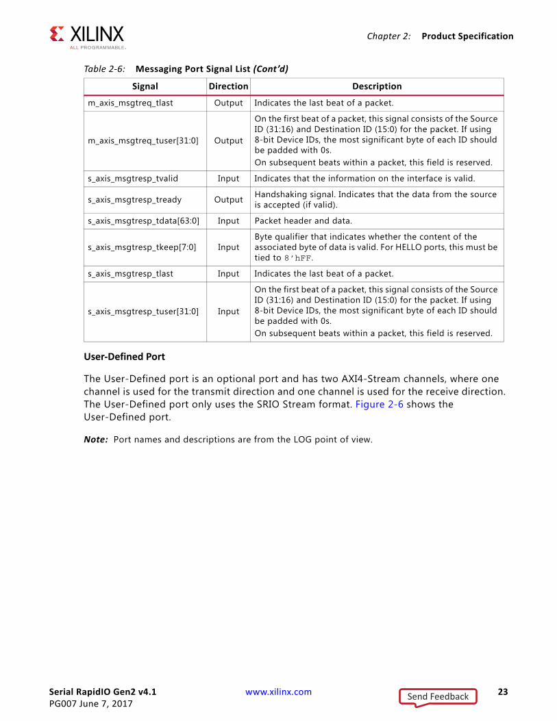
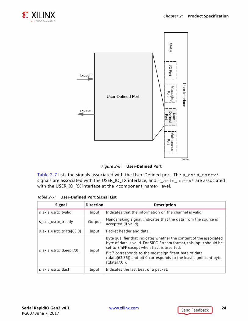
User-Defined Port
The User-Defined port is an optional port and has two AXI4-Stream channels, where one channel is used for the transmit direction and one channel is used for the receive direction. The User-Defined port only uses the SRIO Stream format. Figure 2-6 shows the User-Defined port.
Note: Port names and descriptions are from the LOG point of view.
m_axis_msgtreq_tlast Output Indicates the last beat of a packet.
m_axis_msgtreq_tuser[31:0] Output
On the first beat of a packet, this signal consists of the Source ID (31:16) and Destination ID (15:0) for the packet. If using 8-bit Device IDs, the most significant byte of each ID should be padded with 0s.On subsequent beats within a packet, this field is reserved.
s_axis_msgtresp_tvalid Input Indicates that the information on the interface is valid.
s_axis_msgtresp_tready Output Handshaking signal. Indicates that the data from the source is accepted (if valid).
s_axis_msgtresp_tdata[63:0] Input Packet header and data.
s_axis_msgtresp_tkeep[7:0] InputByte qualifier that indicates whether the content of the associated byte of data is valid. For HELLO ports, this must be tied to 8’hFF.
s_axis_msgtresp_tlast Input Indicates the last beat of a packet.
s_axis_msgtresp_tuser[31:0] Input
On the first beat of a packet, this signal consists of the Source ID (31:16) and Destination ID (15:0) for the packet. If using 8-bit Device IDs, the most significant byte of each ID should be padded with 0s.On subsequent beats within a packet, this field is reserved.
Table 2-6: Messaging Port Signal List (Cont’d)
Signal Direction Description
Send Feedback
Serial RapidIO Gen2 v4.1 www.xilinx.com 24PG007 June 7, 2017
Chapter 2: Product Specification
Table 2-7 lists the signals associated with the User-Defined port. The s_axis_usrtx* signals are associated with the USER_IO_TX interface, and m_axis_usrrx* are associated with the USER_IO_RX interface at the <component_name> level.
X-Ref Target - Figure 2-6
Figure 2-6: User-Defined Port
Table 2-7: User-Defined Port Signal List
Signal Direction Description
s_axis_usrtx_tvalid Input Indicates that the information on the channel is valid.
s_axis_usrtx_tready Output Handshaking signal. Indicates that the data from the source is accepted (if valid).
s_axis_usrtx_tdata[63:0] Input Packet header and data.
s_axis_usrtx_tkeep[7:0] Input
Byte qualifier that indicates whether the content of the associated byte of data is valid. For SRIO Stream format, this input should be set to 8'hFF except when tlast is asserted.Bit 7 corresponds to the most significant byte of data (tdata[63:56]) and bit 0 corresponds to the least significant byte (tdata[7:0]).
s_axis_usrtx_tlast Input Indicates the last beat of a packet.
Send Feedback
Serial RapidIO Gen2 v4.1 www.xilinx.com 25PG007 June 7, 2017
Chapter 2: Product Specification
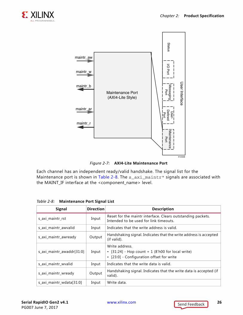
Maintenance Port
If the Maintenance port is enabled, it uses an AXI4-Lite Interface. The AXI4-Lite interface allows the user application to target either the local or remote configuration space.
AXI4-Lite Maintenance Port
Figure 2-7 shows the AXI4-Lite channels associated with the AXI4-Lite Maintenance port. Requests are communicated on the channels shown in black (going right to left), and AXI4-Lite responses are returned on the channels shown in gray (going left to right).
Note: Port names and descriptions are from the LOG point of view.
s_axis_usrtx_tuser[7:0] Input
In SRIO Stream Format, tuser is only 8 bits wide. Bit 1 is used to set the Critical Request Flow (CRF) flag for the packet, and should be tied to zero if CRF support is disabled. All other bits are reserved.On subsequent beats within a packet, this field is reserved.
m_axis_usrrx_tvalid Output Indicates that the information on the channel is valid.
m_axis_usrrx_tready Input Handshaking signal. Indicates that the data from the source is accepted (if valid).
m_axis_usrrx_tdata[63:0] Output Packet header and data.
m_axis_usrrx_tkeep[7:0] Output
Byte qualifier that indicates whether the content of the associated byte of data is valid. For SRIO Stream format, this output is set to 8'hFF except when tlast is asserted.Bit 7 corresponds to the most significant byte of data (tdata[63:56]) and bit 0 corresponds to the least significant byte (tdata[7:0]).
m_axis_usrrx_tlast Output Indicates the last beat of a packet.
m_axis_usrrx_tuser[7:0] Output
In SRIO Stream Format, tuser is only 8 bits wide. Bit 1 is set if the Critical Request Flow (CRF) flag for the packet is set. All other bits are reserved.On subsequent beats within a packet, this field is reserved.
Table 2-7: User-Defined Port Signal List (Cont’d)
Signal Direction Description
Send Feedback
Serial RapidIO Gen2 v4.1 www.xilinx.com 26PG007 June 7, 2017
Chapter 2: Product Specification
Each channel has an independent ready/valid handshake. The signal list for the Maintenance port is shown in Table 2-8. The s_axi_maintr* signals are associated with the MAINT_IF interface at the <component_name> level.
X-Ref Target - Figure 2-7
Figure 2-7: AXI4-Lite Maintenance Port
Table 2-8: Maintenance Port Signal List
Signal Direction Description
s_axi_maintr_rst Input Reset for the maintr interface. Clears outstanding packets. Intended to be used for link timeouts.
s_axi_maintr_awvalid Input Indicates that the write address is valid.
s_axi_maintr_awready Output Handshaking signal. Indicates that the write address is accepted (if valid).
s_axi_maintr_awaddr[31:0] InputWrite address.• [31:24] - Hop count + 1 (8’h00 for local write)• [23:0] - Configuration offset for write
s_axi_maintr_wvalid Input Indicates that the write data is valid.
s_axi_maintr_wready Output Handshaking signal. Indicates that the write data is accepted (if valid).
s_axi_maintr_wdata[31:0] Input Write data.
Send Feedback
Serial RapidIO Gen2 v4.1 www.xilinx.com 27PG007 June 7, 2017
Chapter 2: Product Specification
Status
Table 2-9 lists the signals that provide status information.
s_axi_maintr_bvalid Output Indicates that the write response is valid.
s_axi_maintr_bready Input Handshaking signal. Indicates that the write response is accepted (if valid).
s_axi_maintr_bresp[1:0] Output
Write response.• 2’b00 - OK• 2’b10 - Err• 2’bx1 - Reserved
s_axi_maintr_arvalid Input Indicates that the read address is valid.
s_axi_maintr_arready Output Handshaking signal. Indicates that the read address is accepted (if valid).
s_axi_maintr_araddr[31:0] InputRead address.• [31:24] - Hop count + 1 (8’h00 for local read)• [23:0] - Configuration offset for read
s_axi_maintr_rvalid Output Indicates that the read response is valid.
s_axi_maintr_rready Input Handshaking signal. Indicates that the read response is accepted (if valid).
s_axi_maintr_rresp[1:0] Output
Read response.• 2’b00 - OK• 2’b10 - Err• 2’bx1 - Reserved
s_axi_maintr_rdata[31:0] Output Read Data.
Table 2-9: Status Signal List
Signal Direction Description
deviceid[15:0] Output Current value stored in the Base DeviceID CSR (offset 0x60).
port_decode_error Output Indicates an unsupported transaction was received, and was dropped because the User-Defined port was not enabled. This signal is de-asserted when next supported packet type arrives on any of the user interfaces. This signal is synchronized in log_clk.
Table 2-8: Maintenance Port Signal List
Signal Direction Description
Send Feedback
Serial RapidIO Gen2 v4.1 www.xilinx.com 28PG007 June 7, 2017
Chapter 2: Product Specification
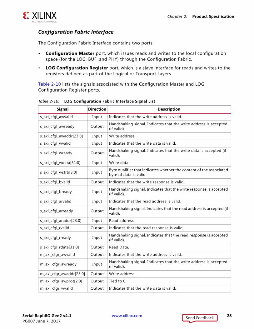
Configuration Fabric Interface
The Configuration Fabric Interface contains two ports:
• Configuration Master port, which issues reads and writes to the local configuration space (for the LOG, BUF, and PHY) through the Configuration Fabric.
• LOG Configuration Register port, which is a slave interface for reads and writes to the registers defined as part of the Logical or Transport Layers.
Table 2-10 lists the signals associated with the Configuration Master and LOG Configuration Register ports.
Table 2-10: LOG Configuration Fabric Interface Signal List
Signal Direction Description
s_axi_cfgl_awvalid Input Indicates that the write address is valid.
s_axi_cfgl_awready Output Handshaking signal. Indicates that the write address is accepted (if valid).
s_axi_cfgl_awaddr[23:0] Input Write address.
s_axi_cfgl_wvalid Input Indicates that the write data is valid.
s_axi_cfgl_wready Output Handshaking signal. Indicates that the write data is accepted (if valid).
s_axi_cfgl_wdata[31:0] Input Write data.
s_axi_cfgl_wstrb[3:0] Input Byte qualifier that indicates whether the content of the associated byte of data is valid.
s_axi_cfgl_bvalid Output Indicates that the write response is valid.
s_axi_cfgl_bready Input Handshaking signal. Indicates that the write response is accepted (if valid).
s_axi_cfgl_arvalid Input Indicates that the read address is valid.
s_axi_cfgl_arready Output Handshaking signal. Indicates that the read address is accepted (if valid).
s_axi_cfgl_araddr[23:0] Input Read address.
s_axi_cfgl_rvalid Output Indicates that the read response is valid.
s_axi_cfgl_rready Input Handshaking signal. Indicates that the read response is accepted (if valid).
s_axi_cfgl_rdata[31:0] Output Read Data.
m_axi_cfgr_awvalid Output Indicates that the write address is valid.
m_axi_cfgr_awready Input Handshaking signal. Indicates that the write address is accepted (if valid).
m_axi_cfgr_awaddr[23:0] Output Write address.
m_axi_cfgr_awprot[2:0] Output Tied to 0.
m_axi_cfgr_wvalid Output Indicates that the write data is valid.
Send Feedback
Serial RapidIO Gen2 v4.1 www.xilinx.com 29PG007 June 7, 2017
Chapter 2: Product Specification
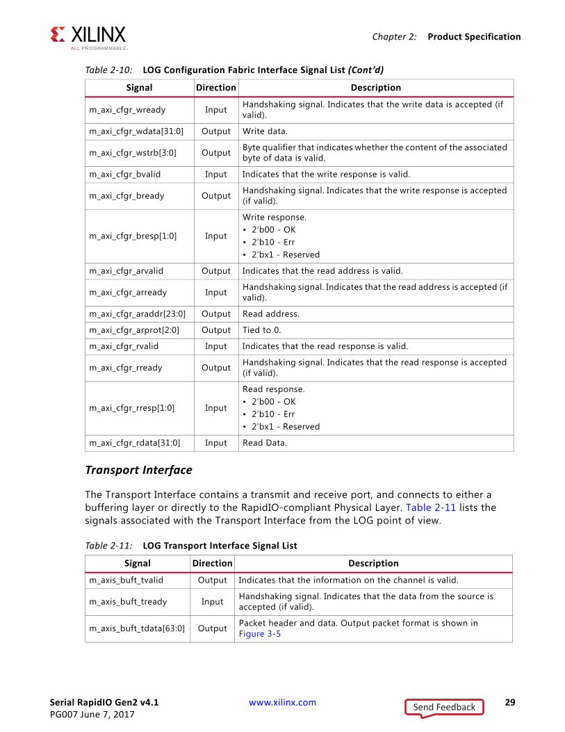
Transport Interface
The Transport Interface contains a transmit and receive port, and connects to either a buffering layer or directly to the RapidIO-compliant Physical Layer. Table 2-11 lists the signals associated with the Transport Interface from the LOG point of view.
m_axi_cfgr_wready Input Handshaking signal. Indicates that the write data is accepted (if valid).
m_axi_cfgr_wdata[31:0] Output Write data.
m_axi_cfgr_wstrb[3:0] Output Byte qualifier that indicates whether the content of the associated byte of data is valid.
m_axi_cfgr_bvalid Input Indicates that the write response is valid.
m_axi_cfgr_bready Output Handshaking signal. Indicates that the write response is accepted (if valid).
m_axi_cfgr_bresp[1:0] Input
Write response.• 2’b00 - OK• 2’b10 - Err• 2’bx1 - Reserved
m_axi_cfgr_arvalid Output Indicates that the read address is valid.
m_axi_cfgr_arready Input Handshaking signal. Indicates that the read address is accepted (if valid).
m_axi_cfgr_araddr[23:0] Output Read address.
m_axi_cfgr_arprot[2:0] Output Tied to 0.
m_axi_cfgr_rvalid Input Indicates that the read response is valid.
m_axi_cfgr_rready Output Handshaking signal. Indicates that the read response is accepted (if valid).
m_axi_cfgr_rresp[1:0] Input
Read response.• 2’b00 - OK• 2’b10 - Err• 2’bx1 - Reserved
m_axi_cfgr_rdata[31:0] Input Read Data.
Table 2-11: LOG Transport Interface Signal List
Signal Direction Description
m_axis_buft_tvalid Output Indicates that the information on the channel is valid.
m_axis_buft_tready Input Handshaking signal. Indicates that the data from the source is accepted (if valid).
m_axis_buft_tdata[63:0] Output Packet header and data. Output packet format is shown in Figure 3-5
Table 2-10: LOG Configuration Fabric Interface Signal List (Cont’d)
Signal Direction Description
Send Feedback
Serial RapidIO Gen2 v4.1 www.xilinx.com 30PG007 June 7, 2017
Chapter 2: Product Specification
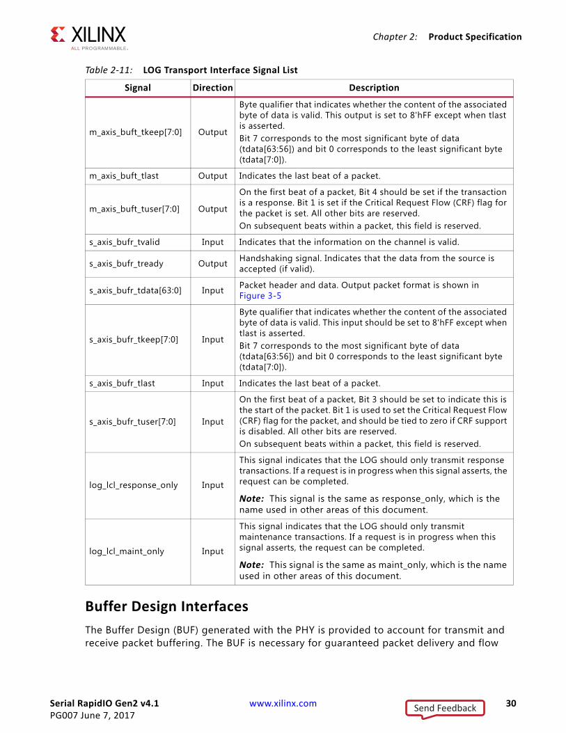
Buffer Design InterfacesThe Buffer Design (BUF) generated with the PHY is provided to account for transmit and receive packet buffering. The BUF is necessary for guaranteed packet delivery and flow
m_axis_buft_tkeep[7:0] Output
Byte qualifier that indicates whether the content of the associated byte of data is valid. This output is set to 8'hFF except when tlast is asserted.Bit 7 corresponds to the most significant byte of data (tdata[63:56]) and bit 0 corresponds to the least significant byte (tdata[7:0]).
m_axis_buft_tlast Output Indicates the last beat of a packet.
m_axis_buft_tuser[7:0] Output
On the first beat of a packet, Bit 4 should be set if the transaction is a response. Bit 1 is set if the Critical Request Flow (CRF) flag for the packet is set. All other bits are reserved.On subsequent beats within a packet, this field is reserved.
s_axis_bufr_tvalid Input Indicates that the information on the channel is valid.
s_axis_bufr_tready Output Handshaking signal. Indicates that the data from the source is accepted (if valid).
s_axis_bufr_tdata[63:0] Input Packet header and data. Output packet format is shown in Figure 3-5
s_axis_bufr_tkeep[7:0] Input
Byte qualifier that indicates whether the content of the associated byte of data is valid. This input should be set to 8'hFF except when tlast is asserted.Bit 7 corresponds to the most significant byte of data (tdata[63:56]) and bit 0 corresponds to the least significant byte (tdata[7:0]).
s_axis_bufr_tlast Input Indicates the last beat of a packet.
s_axis_bufr_tuser[7:0] Input
On the first beat of a packet, Bit 3 should be set to indicate this is the start of the packet. Bit 1 is used to set the Critical Request Flow (CRF) flag for the packet, and should be tied to zero if CRF support is disabled. All other bits are reserved.On subsequent beats within a packet, this field is reserved.
log_lcl_response_only Input
This signal indicates that the LOG should only transmit response transactions. If a request is in progress when this signal asserts, the request can be completed.
Note: This signal is the same as response_only, which is the name used in other areas of this document.
log_lcl_maint_only Input
This signal indicates that the LOG should only transmit maintenance transactions. If a request is in progress when this signal asserts, the request can be completed.
Note: This signal is the same as maint_only, which is the name used in other areas of this document.
Table 2-11: LOG Transport Interface Signal List
Signal Direction Description
Send Feedback
Serial RapidIO Gen2 v4.1 www.xilinx.com 31PG007 June 7, 2017
Chapter 2: Product Specification
control operations. Xilinx provides a configurable buffer solution that allows for trade-offs between system performance and resource requirements.
The transmit buffer is responsible for queuing outgoing transactions and managing the flow of these packets over the link interface into the PHY. TX and RX Buffer sizes are configurable through the Vivado IDE to values of 8, 16 or 32 packets in depth. The TX buffer is a store and forward buffer designed for a low packet-to-packet latency to maximize streaming throughput. The transmit buffer must hold each packet until it has been successfully received by the link partner device, at which point the packet is released to make room for additional packets. In the case where multiple unsent packets accumulate in the buffer, which often happens when flow control occurs, the BUF reorders packets based on type and priority with response packets issued first followed by requests. For more information on flow control and packet reordering, see Chapter 3, Designing with the Core.
Additionally the BUF handles clock crossing when necessary. Clock domain crossing logic can be added or removed when generating the core.
RECOMMENDED: Clock domain crossing logic is recommended for all multi-lane cores because the PHY clock is dynamic at start-up and during traindown scenarios. This allows the user logic to run at a consistent and known rate.
The receive buffer acts as a FIFO for storing and forwarding data into the LOG receive path. The receive buffer also has domain crossing logic which allows the logical layer/user design and the PHY to run at different clock rates. As with the transmit buffer design, this logic is recommended for multi-lane cores.
All interfaces for the BUF are connected internally to the <component_name>_block module and are invisible from outside the wrapper layer.
Send Feedback
Serial RapidIO Gen2 v4.1 www.xilinx.com 32PG007 June 7, 2017
Chapter 2: Product Specification
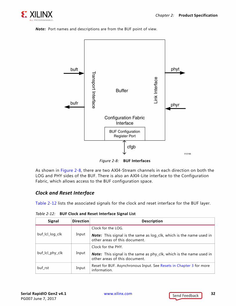
Note: Port names and descriptions are from the BUF point of view.
As shown in Figure 2-8, there are two AXI4-Stream channels in each direction on both the LOG and PHY sides of the BUF. There is also an AXI4-Lite interface to the Configuration Fabric, which allows access to the BUF configuration space.
Clock and Reset Interface
Table 2-12 lists the associated signals for the clock and reset interface for the BUF layer.
X-Ref Target - Figure 2-8
Figure 2-8: BUF Interfaces
Table 2-12: BUF Clock and Reset Interface Signal List
Signal Direction Description
buf_lcl_log_clk Input
Clock for the LOG.
Note: This signal is the same as log_clk, which is the name used in other areas of this document.
buf_lcl_phy_clk Input
Clock for the PHY.
Note: This signal is the same as phy_clk, which is the name used in other areas of this document.
buf_rst Input Reset for BUF. Asynchronous Input. See Resets in Chapter 3 for more information.
Send Feedback
Serial RapidIO Gen2 v4.1 www.xilinx.com 33PG007 June 7, 2017
Chapter 2: Product Specification
Transport Interface
Table 2-13 lists the signals associated with the BUF Transport Interface.
buf_lcl_cfg_clk Input
Configuration Register Interface clock. If the AXI4-Lite Maintenance Port and the Configuration Fabric reference design are in use, this must be equivalent to log_clk. Otherwise, this clock is independent of log_clk.
Note: This signal is the same as cfg_clk, which is the name used in other areas of this document.
buf_lcl_cfg_rst Input
Configuration Register Interface reset. Clears BUF registers to default values. Must deassert synchronously to cfg_clk.
Note: This signal is the same as cfg_rst, which is the name used in other areas of this document.
Table 2-13: BUF Transport Interface Signal List
Signal Direction Description
s_axis_buft_tvalid Input Indicates that the information on the channel is valid.
s_axis_buft_tready Output Handshaking signal. Indicates that the data from the source is accepted (if valid).
s_axis_buft_tdata[63:0] Input Packet header and data.
s_axis_buft_tkeep[7:0] Input
Byte qualifier that indicates whether the content of the associated byte of data is valid. This output is set to 8'hFF except when tlast is asserted.Bit 7 corresponds to the most significant byte of data (tdata[63:56]) and bit 0 corresponds to the least significant byte (tdata[7:0]).
s_axis_buft_tlast Input Indicates the last beat of a packet.
s_axis_buft_tuser[7:0] Input
On the first beat of a packet, Bit 4 should be set if the transaction is a response. If Bit 1 is High, the Critical Request Flow (CRF) flag for the packet is set (if CRF Support is enabled). All other bits are reserved.On subsequent beats within a packet, this field is reserved.
m_axis_bufr_tvalid Output Indicates that the information on the channel is valid.
m_axis_bufr_tready Input Handshaking signal. Indicates that the data from the source is accepted (if valid).
m_axis_bufr_tdata[63:0] Output Packet header and data.
m_axis_bufr_tkeep[7:0] Output
Byte qualifier that indicates whether the content of the associated byte of data is valid. This input should be set to 8'hFF except when tlast is asserted.Bit 7 corresponds to the most significant byte of data (tdata[63:56]) and bit 0 corresponds to the least significant byte (tdata[7:0]).
m_axis_bufr_tlast Output Indicates the last beat of a packet.
Table 2-12: BUF Clock and Reset Interface Signal List (Cont’d)
Signal Direction Description
Send Feedback
Serial RapidIO Gen2 v4.1 www.xilinx.com 34PG007 June 7, 2017
Chapter 2: Product Specification
Link Interface
Table 2-14 lists the signals associated with the BUF Link Interface.
m_axis_bufr_tuser[7:0] Output
On the first beat of a packet, Bit 3 is set to indicate this is the start of packet. Bit 1 reflects the value of the Critical Request Flow (CRF) flag for the packet, if CRF support is enabled. All other bits are reserved.On subsequent beats within a packet, this field is reserved.
buf_lcl_response_only Output
This signal indicates that the transmit buffer can only accept responses. If a request is in progress when this signal asserts, the request can be completed.
Note: This signal is the same as response_only, which is the name used in other areas of this document.
Table 2-14: BUF Link Interface Signal List
Signal Direction Description
m_axis_phyt_tvalid Output Indicates that the information on the channel is valid.
m_axis_phyt_tready Input Handshaking signal. Indicates that the data from the source is accepted (if valid).
m_axis_phyt_tdata[63:0] Output Packet header and data.
m_axis_phyt_tkeep[7:0] Output
Byte qualifier that indicates whether the content of the associated byte of data is valid. This input should be set to 8'hFF except when tlast is asserted.Bit 7 corresponds to the most significant byte of data (tdata[63:56]) and bit 0 corresponds to the least significant byte (tdata[7:0]).
m_axis_phyt_tlast Output Indicates the last beat of a packet.
m_axis_phyt_tuser[7:0] Output
On the first beat of a packet, Bit 1 reflects the value of the Critical Request Flow (CRF) flag for the packet, if CRF support is enabled. All other bits are reserved.On the last beat of a packet, Bit 0 is used as a source discontinue. If Bit 0 is High on the tlast transfer, the packet should be discarded.
s_axis_phyr_tvalid Input Indicates that the information on the channel is valid.
s_axis_phyr_tready Output Handshaking signal. Indicates that the data from the source is accepted (if valid).
s_axis_phyr_tdata[63:0] Input Packet header and data.
Table 2-13: BUF Transport Interface Signal List (Cont’d)
Signal Direction Description
Send Feedback

Serial RapidIO Gen2 v4.1 www.xilinx.com 35PG007 June 7, 2017
Chapter 2: Product Specification
s_axis_phyr_tkeep[7:0] Input
Byte qualifier that indicates whether the content of the associated byte of data is valid. This output is set to 8'hFF except when tlast is asserted.Bit 7 corresponds to the most significant byte of data (tdata[63:56]) and bit 0 corresponds to the least significant byte (tdata[7:0]).
s_axis_phyr_tlast Input Indicates the last beat of a packet.
s_axis_phyr_tuser[7:0] Input
If Bit 1 is High on the first beat of a packet, the Critical Request Flow (CRF) flag for the packet is set (if CRF Support is enabled). All other bits are reserved.On the last beat of a packet, Bit 0 is used as a source discontinue. If Bit 0 is High on the tlast transfer, the packet is dropped in the BUF.
buf_lcl_master_enable Input
Reflects the value of the Master Enable bit from the Port General Control CSR in the physical layer configuration space. When set, the BUF can forward requests to the PHY. If this input is Low, the BUF can only forward responses.
Note: This signal is the same as master_enable, which is the name used in other areas of this document.
buf_lcl_idle2_selected Input
When asserted, the PHY is operating in IDLE2 mode and using long control symbols (therefore ackIDs are 6 bits).
Note: This signal is the same as idle2_selected, which is the name used in other areas of this document.
buf_lcl_phy_rewind Input
This signal indicates that the PHY is requesting a rewind. The BUF must monitor the next_fm signal to determine which packet to transmit next.
Note: This signal is the same as phy_rewind, which is the name used in other areas of this document.
buf_lcl_phy_next_fm Input
This bus is used to communicate the next packet to send, indexed by ackID. This signal increments for each packet, except in a rewind scenario.
Note: This signal is the same as phy_next_fm, which is the name used in other areas of this document.
buf_lcl_phy_last_ack Input
This bus is used to communicate the ackID for the last acknowledge control symbol received. This frees up slots in the buffer by allowing the BUF to clear the corresponding packet. If this signal increments by more than one, multiple packet can be cleared.
Note: This signal is the same as phy_last_ack, which is the name used in other areas of this document.
buf_lcl_phy_rcvd_buf_stat Input
This bus is used to communicate the last received buffer status from a status control symbol received from the link partner.
Note: This signal is the same as phy_rcvd_buf_stat, which is the name used in other areas of this document.
Table 2-14: BUF Link Interface Signal List (Cont’d)
Signal Direction Description
Send Feedback
Serial RapidIO Gen2 v4.1 www.xilinx.com 36PG007 June 7, 2017
Chapter 2: Product Specification
BUF Configuration Fabric Interface
Table 2-15 lists the signals associated with the Configuration Fabric Interface.
Note: All the signal names in Table 2-15 are from the BUF point of view.
buf_lcl_phy_buf_stat Output
This bus is used to communicate the status of the Receive Buffer. This bus is never equal to all ones, which indicates receiver flow control. Nor is the lower five bits all ones, which might also be perceived as receiver flow control. It always holds an estimation of number of free buffer locations. When the buffer is very lean (more than 30 free packet locations), the buf_stat value provides the value of 30.
Note: This signal is the same as phy_buf_stat, which is the name used in other areas of this document.
buf_lcl_tx_flow_control Output
Indicates that the transmit buffer is in transmitter-controlled flow control mode.
Note: This signal is the same as tx_flow_control, which is the name used in other areas of this document.
Table 2-15: BUF Configuration Fabric Interface Signal List
Signal Direction Description
s_axi_cfgb_awvalid Input Indicates that the write address is valid.
s_axi_cfgb_awready Output Handshaking signal. Indicates that the write address is accepted (if valid).
s_axi_cfgb_awaddr[23:0] Input Write address.
s_axi_cfgb_wvalid Input Indicates that the write data is valid.
s_axi_cfgb_wready Output Handshaking signal. Indicates that the write data is accepted (if valid).
s_axi_cfgb_wdata[31:0] Input Write data.
s_axi_cfgb_wstrb[3:0] Input Byte qualifier that indicates whether the content of the associated byte of data is valid.
s_axi_cfgb_bvalid Output Indicates that the write response is valid.
s_axi_cfgb_bready Input Handshaking signal. Indicates that the write response is accepted (if valid).
s_axi_cfgb_arvalid Input Indicates that the read address is valid.
s_axi_cfgb_arready Output Handshaking signal. Indicates that the read address is accepted (if valid).
s_axi_cfgb_araddr[23:0] Input Read address.
s_axi_cfgb_rvalid Output Indicates that the read response is valid.
Table 2-14: BUF Link Interface Signal List (Cont’d)
Signal Direction Description
Send Feedback
Serial RapidIO Gen2 v4.1 www.xilinx.com 37PG007 June 7, 2017
Chapter 2: Product Specification
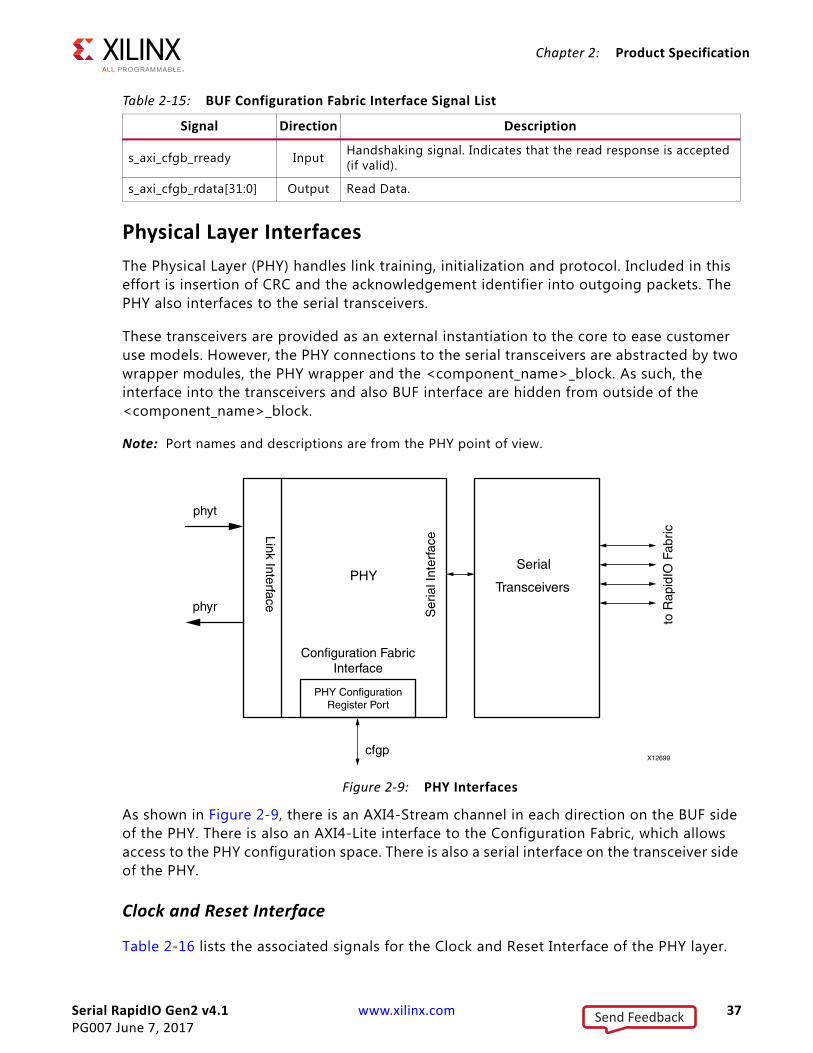
Physical Layer InterfacesThe Physical Layer (PHY) handles link training, initialization and protocol. Included in this effort is insertion of CRC and the acknowledgement identifier into outgoing packets. The PHY also interfaces to the serial transceivers.
These transceivers are provided as an external instantiation to the core to ease customer use models. However, the PHY connections to the serial transceivers are abstracted by two wrapper modules, the PHY wrapper and the <component_name>_block. As such, the interface into the transceivers and also BUF interface are hidden from outside of the <component_name>_block.
Note: Port names and descriptions are from the PHY point of view.
As shown in Figure 2-9, there is an AXI4-Stream channel in each direction on the BUF side of the PHY. There is also an AXI4-Lite interface to the Configuration Fabric, which allows access to the PHY configuration space. There is also a serial interface on the transceiver side of the PHY.
Clock and Reset Interface
Table 2-16 lists the associated signals for the Clock and Reset Interface of the PHY layer.
s_axi_cfgb_rready Input Handshaking signal. Indicates that the read response is accepted (if valid).
s_axi_cfgb_rdata[31:0] Output Read Data.
X-Ref Target - Figure 2-9
Figure 2-9: PHY Interfaces
Table 2-15: BUF Configuration Fabric Interface Signal List
Signal Direction Description
Send Feedback

Serial RapidIO Gen2 v4.1 www.xilinx.com 38PG007 June 7, 2017
Chapter 2: Product Specification
GT Common Clock Interface
Table 2-17 lists the associated signals for the GT Common Clock Interface.
Table 2-16: PHY Clock and Reset Interface Signal List
Signal Direction Description
phy_lcl_phy_clk Input
Frequency depends on serial transfer frequency and initialized link width. If the core trains down to 1x mode, phy_clk must change to the 1x rate. See Clocking in Chapter 3 for more information.
Note: This signal is the same as phy_clk, which is the name used in other areas of this document.
phy_rst Input Reset for PHY. Must deassert synchronously to phy_clk. See Resets in Chapter 3 for more information.
gt_pcs_clk Input
Clock signal for Serial Interface. Must be phase aligned to phy_clk. The clock rate is based on the transfer frequency of the core, and is half of the gt_clk:• 1.25 G - 31.25 MHz• 2.5 G - 62.5 MHz• 3.125 G - 78.13 MHz• 5 G - 125 MHz• 6.25 G - 156.MHz
gt_pcs_rst Input Reset for Serial Interface. Must deassert synchronously to gt_pcs_clk. See Resets in Chapter 3 for more information.
phy_lcl_cfg_clk Input
Configuration Register Interface clock. If the AXI4-Lite Maintenance Port and the Configuration Fabric reference design are in use, this must be equivalent to log_clk. Otherwise, this clock is independent of log_clk.
Note: This signal is the same as cfg_clk, which is the name used in other areas of this document.
phy_lcl_cfg_rst Input
Configuration Register Interface reset. Clears PHY registers to default values. Must deassert synchronously to cfg_clk.
Note: This signal is the same as cfg_rst, which is the name used in other areas of this document.
Table 2-17: GT Common Clock Interface Signal List
Signal Direction Description
gt0_pll0_clk Input Valid only for Artix7 families. Indicates clock from PLL0 of GT Common
gt0_pll0_refclk Input Valid only for Artix7 families. Indicates reference clock from PLL0 of GT Common
gt0_pll1_clk Input Valid only for Artix7 families. Indicates clock from PLL1 of GT Common
gt0_pll1_refclk Input Valid only for Artix7 families. Indicates reference clock from PLL1 of GT Common
Send Feedback
Serial RapidIO Gen2 v4.1 www.xilinx.com 39PG007 June 7, 2017
Chapter 2: Product Specification
Link Interface
Table 2-18 lists the signals associated with the PHY Link Interface.
gt0_pll0_lock Input Valid only for Artix7 families. Indicates PLL0 of GT Common has locked
gt0_pll0_reset_out Output Valid only for Artix7 families. Reset input to GT Common
gt0_qpll_clk Input Valid only for non Artix7 families. Indicates clock from PLL of GT Common
gt0_qpll_out_refclk Input Valid only for non Artix7 families. Indicates reference out clock from PLL of GT Common
gt0_qpll_lock Input Valid only for non Artix7 families. Indicates clock lock from PLL of GT Common
Table 2-18: PHY Link Interface Signal List
Signal Direction Description
s_axis_phyt_tvalid Input Indicates that information on the channel is valid.
s_axis_phyt_tready Output Handshaking signal. Indicates that the data from the source is accepted (if valid).
s_axis_phyt_tdata[63:0] Input Packet header and data.
s_axis_phyt_tkeep[7:0] Input
Byte qualifier that indicates whether the content of the associated byte of data is valid. This input should be set to 8'hFF except when tlast is asserted.Bit 7 corresponds to the most significant byte of data (tdata[63:56]) and bit 0 corresponds to the least significant byte (tdata[7:0]).
s_axis_phyt_tlast Input Indicates the last beat of a packet.
s_axis_phyt_tuser[7:0] Input
On the first beat of a packet, Bit 1 reflects the value of the Critical Request Flow (CRF) flag for the packet, if CRF support is enabled. All other bits are reserved.On the last beat of a packet, Bit 0 is used as a source discontinue. If Bit 0 is High on the tlast transfer, the packet should be discarded.
m_axis_phyr_tvalid Output Indicates that the information on the channel is valid.
m_axis_phyr_tready Input Handshaking signal. Indicates that the data from the source is accepted (if valid).
m_axis_phyr_tdata[63:0] Output Packet header and data.
m_axis_phyr_tkeep[7:0] Output
Byte qualifier that indicates whether the content of the associated byte of data is valid. This output is set to 8'hFF except when tlast is asserted.Bit 7 corresponds to the most significant byte of data (tdata[63:56]) and bit 0 corresponds to the least significant byte (tdata[7:0]).
Table 2-17: GT Common Clock Interface Signal List (Cont’d)
Signal Direction Description
Send Feedback
Serial RapidIO Gen2 v4.1 www.xilinx.com 40PG007 June 7, 2017
Chapter 2: Product Specification
m_axis_phyr_tlast Output Indicates the last beat of a packet.
m_axis_phyr_tuser[7:0] Output
If Bit 1 is High on the first beat of a packet, the Critical Request Flow (CRF) flag for the packet is set (if CRF Support is enabled). All other bits are reserved.On the last beat of a packet, Bit 0 is used as a source discontinue. If Bit 0 is High on the tlast transfer, the packet is dropped in the BUF.
srio_host OutputReflects the value of the Host bit from the Port General Control CSR in the physical layer configuration space. When set, the endpoint is the system host device.
phy_lcl_master_enable Output
Reflects the value of the Master Enable bit from the Port General Control CSR in the physical layer configuration space. When set, the BUF can forward requests to the PHY. If this input is Low, the BUF can only forward responses.
Note: This signal is the same as master_enable, which is the name used in other areas of this document.
phy_lcl_idle2_selected Output
When asserted, the PHY is operating in IDLE2 mode and using long control symbols (therefore ackIDs are 6 bits).
Note: This signal is the same as idle2_selected, which is the name used in other areas of this document.
phy_lcl_phy_rewind Output
This signal indicates that the PHY is requesting a rewind. The BUF must monitor the next_fm signal to determine which packet to transmit next.
Note: This signal is the same as phy_rewind, which is the name used in other areas of this document.
phy_lcl_phy_next_fm Output
This bus is used to communicate the next packet to send, indexed by ackID. This signal increments for each packet, except in a rewind scenario.
Note: This signal is the same as phy_next_fm, which is the name used in other areas of this document.
phy_lcl_phy_last_ack Output
This bus is used to communicate the ackID for the last acknowledge control symbol received. This frees up slots in the buffer by allowing the BUF to clear the corresponding packet. If this signal increments by more than one, multiple packet can be cleared.
Note: This signal is the same as phy_last_ack, which is the name used in other areas of this document.
phy_lcl_phy_rcvd_buf_stat Output
This bus is used to communicate the last received buffer status from a status control symbol received from the link partner.
Note: This signal is the same as phy_rcvd_buf_stat, which is the name used in other areas of this document.
Table 2-18: PHY Link Interface Signal List (Cont’d)
Signal Direction Description
Send Feedback
Serial RapidIO Gen2 v4.1 www.xilinx.com 41PG007 June 7, 2017
Chapter 2: Product Specification
Serial Interface
Table 2-19 lists the signals associated with the Serial Interface.
Note: LW = link width.
phy_lcl_phy_buf_stat Input
This bus is used to communicate the status of the Receive Buffer. This bus is never equal to all ones, which indicates receiver flow control. Nor are the lower five bits all ones, which might also be perceived as receiver flow control. It always holds an estimation of number of free buffer locations. When the buffer is very lean (more than 30 free packet locations), the buf_stat value provides the value of 30.
Note: This signal is the same as phy_buf_stat, which is the name used in other areas of this document.
phy_lcl_tx_flow_control Input
Indicates that the transmit buffer is in transmitter-controlled flow control mode.
Note: This signal is the same as tx_flow_control, which is the name used in other areas of this document.
Table 2-19: PHY Serial Interface Signal List
Signal Direction Description
gttx_data[32*LW-1:0] Output Transmit data to the serial transceivers.
gttx_charisk[4*LW-1:0] Output Per-byte K-character indicator to the serial transceivers. If bit 0 is asserted, gttx_data[7:0] is a K-character, and so on.
gttx_inhibit[LW-1:0] Output Per-lane inhibit for the serial transceivers. If bit 0 is asserted, the transmitter of lane0 is disabled, and so on.
gtrx_data[32*LW-1:0] Input Receive data from the serial transceivers.
gtrx_charisk[4*LW-1:0] Input Per-byte K-character indicator from the serial transceivers. If bit 0 is asserted, gtrx_data[7:0] is a K-character, and so on.
gtrx_chariscomma[4*LW-1:0] Input Per-byte comma indicator from the serial transceivers. If bit 0 is asserted, gtrx_data[7:0] is a comma character, and so on.
gtrx_disperr[4*LW-1:0] InputPer-byte disparity error indicator from the serial transceivers. If bit 0 is asserted, gtrx_data[7:0] had a disparity error, and so on.
gtrx_notintable[4*LW-1:0] InputPer-byte not-in-table error indicator from the serial transceivers. If bit 0 is asserted, gtrx_data[7:0] had an 8b/10b decode error, and so on.
gtrx_chanbondseq[LW-1:0] InputPer-lane channel bonding sequence indicator from the serial transceivers. If bit 0 is asserted, lane0 received a channel bonding sequence, and so on.
gtrx_chanisaligned[LW-1:0] InputPer-lane alignment indicator from the serial transceivers. If bit 0 is asserted, lane0 is aligned with the channel bonding master, and so on.
Table 2-18: PHY Link Interface Signal List (Cont’d)
Signal Direction Description
Send Feedback

Serial RapidIO Gen2 v4.1 www.xilinx.com 42PG007 June 7, 2017
Chapter 2: Product Specification
Control and Status Interface
Table 2-20 list the signals associated with the PHY Control/Status Interface.
gtrx_chanbonden Output Enable channel bonding in the serial transceivers.
gtrx_reset_req Input The serial transceivers require a reset, for example due to an elastic buffer underflow or overflow.
gtrx_reset Output Reset for the serial transceivers.
gtrx_reset_done[LW-1:0] InputPer-lane indicator that the reset sequence is complete for the serial transceiver. If bit 0 is asserted, lane0 is finished with the reset process, and so on.
Table 2-20: PHY Control and Status Interface Signal List
Signal Direction Description
sim_train_en Input This signal reduces the timers for initialization. This signal is tied to 1 in srio_sim.v for simulation purposes. Otherwise, this signal is assigned to 0 inside the core. You should leave it unconnected or tie it to 0 for hardware implementation.
phy_mce Input This is a single-cycle input signal that instructs the PHY to send an MCE control signal.
phy_link_reset Input As long as this signal is asserted, the PHY sends Link Reset control symbols.
force_reinit Input This signal forces the PHY to reinitialize the link.
link_initialized Output Indicates the link has initialized. Specifically, at least 15 Status control symbols have been sent and 8 error-free Status control symbols have been received.
phy_rcvd_mce Output Indicates the PHY has received an MCE control symbol from the link partner.
phy_rcvd_link_reset Output Indicates the PHY has received at least four consecutive, error-free Link Reset control symbols.
Note: Status control symbols and Idles are permitted to be interspersed between these Link Reset control symbols.
port_error Output Indicates the port has received an unrecoverable error and is in the error state. This signal reflects the value of the Port Error bit in the Port n Error and Status CSR in the Physical Layer configuration.
port_initialized Output Indicates the port has initialized. This signal reflects the value of the Port Uninitialized bit in the Port n Error and Status CSR in the Physical Layer configuration
mode_1x Output Indicates the link has trained down to 1x.
idle_selected Output Indicates that either IDLE1 or IDLE2 has been selected.
port_timeout[23:0] Output Reflects the value of the Timeout Value field in the Port Link Timeout Control CSR.
Table 2-19: PHY Serial Interface Signal List (Cont’d)
Signal Direction Description
Send Feedback

Serial RapidIO Gen2 v4.1 www.xilinx.com 43PG007 June 7, 2017
Chapter 2: Product Specification
Configuration Fabric Interface
Table 2-21 lists the signals associated with the Configuration Fabric Interface.
srio_host Output Reflects the value of the Host bit from the Port General Control CSR in the Physical Layer configuration
phy_lcl_maint_only Output This signal indicates that the LOG should only transmit maintenance transactions. If a request is in progress when this signal asserts, the request can be completed.
Note: This signal is the same as maint_only, which is the name used in other areas of this document.
rx_lane_r Output Indicates the port has trained down to the redundancy lane.
Table 2-21: PHY Configuration Fabric Interface Signal List
Signal Direction Description
s_axi_cfgp_awvalid Input Indicates that the write address is valid.
s_axi_cfgp_awready Output Handshaking signal. Indicates that the write address is accepted (if valid).
s_axi_cfgp_awaddr[23:0] Input Write address.
s_axi_cfgp_wvalid Input Indicates that the write data is valid.
s_axi_cfgp_wready Output Handshaking signal. Indicates that the write data is accepted (if valid).
s_axi_cfgp_wdata[31:0] Input Write data.
s_axi_cfgp_wstrb[3:0] Input Byte qualifier that indicates whether the content of the associated byte of data is valid.
s_axi_cfgp_bvalid Output Indicates that the write response is valid.
s_axi_cfgp_bready Input Handshaking signal. Indicates that the write response is accepted (if valid).
s_axi_cfgp_arvalid Input Indicates that the read address is valid.
s_axi_cfgp_arready Output Handshaking signal. Indicates that the read address is accepted (if valid).
s_axi_cfgp_araddr[23:0] Input Read address.
s_axi_cfgp_rvalid Output Indicates that the read response is valid.
s_axi_cfgp_rready Input Handshaking signal. Indicates that the read response is accepted (if valid).
s_axi_cfgp_rdata[31:0] Output Read Data.
Table 2-20: PHY Control and Status Interface Signal List (Cont’d)
Signal Direction Description
Send Feedback
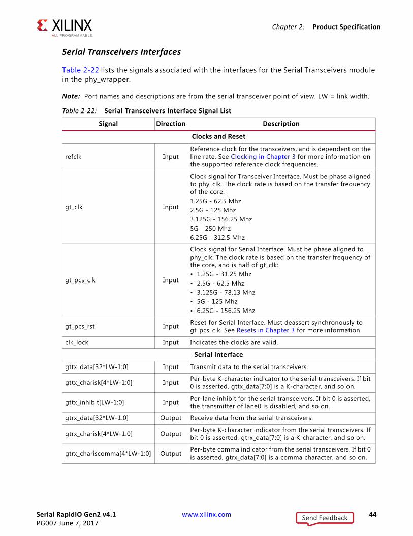
Serial RapidIO Gen2 v4.1 www.xilinx.com 44PG007 June 7, 2017
Chapter 2: Product Specification
Serial Transceivers Interfaces
Table 2-22 lists the signals associated with the interfaces for the Serial Transceivers module in the phy_wrapper.
Note: Port names and descriptions are from the serial transceiver point of view. LW = link width.
Table 2-22: Serial Transceivers Interface Signal List
Signal Direction Description
Clocks and Reset
refclk InputReference clock for the transceivers, and is dependent on the line rate. See Clocking in Chapter 3 for more information on the supported reference clock frequencies.
gt_clk Input
Clock signal for Transceiver Interface. Must be phase aligned to phy_clk. The clock rate is based on the transfer frequency of the core:1.25G - 62.5 Mhz2.5G - 125 Mhz3.125G - 156.25 Mhz5G - 250 Mhz6.25G - 312.5 Mhz
gt_pcs_clk Input
Clock signal for Serial Interface. Must be phase aligned to phy_clk. The clock rate is based on the transfer frequency of the core, and is half of gt_clk:• 1.25G - 31.25 Mhz• 2.5G - 62.5 Mhz• 3.125G - 78.13 Mhz• 5G - 125 Mhz• 6.25G - 156.25 Mhz
gt_pcs_rst Input Reset for Serial Interface. Must deassert synchronously to gt_pcs_clk. See Resets in Chapter 3 for more information.
clk_lock Input Indicates the clocks are valid.
Serial Interface
gttx_data[32*LW-1:0] Input Transmit data to the serial transceivers.
gttx_charisk[4*LW-1:0] Input Per-byte K-character indicator to the serial transceivers. If bit 0 is asserted, gttx_data[7:0] is a K-character, and so on.
gttx_inhibit[LW-1:0] Input Per-lane inhibit for the serial transceivers. If bit 0 is asserted, the transmitter of lane0 is disabled, and so on.
gtrx_data[32*LW-1:0] Output Receive data from the serial transceivers.
gtrx_charisk[4*LW-1:0] Output Per-byte K-character indicator from the serial transceivers. If bit 0 is asserted, gtrx_data[7:0] is a K-character, and so on.
gtrx_chariscomma[4*LW-1:0] Output Per-byte comma indicator from the serial transceivers. If bit 0 is asserted, gtrx_data[7:0] is a comma character, and so on.
Send Feedback
Serial RapidIO Gen2 v4.1 www.xilinx.com 45PG007 June 7, 2017
Chapter 2: Product Specification
Configuration Fabric Reference Design InterfacesThe Configuration Fabric reference design manages the accesses to the configuration spaces of each of the sub-cores. The configuration modules in each of the sub-cores are slaves on the configuration bus (an AXI-Lite interface), and the Configuration Fabric module is the bus master. Reads and writes derived from Maintenance transactions that were issued either locally or from the link partner are presented to the Configuration Fabric through the Configuration Master port in the LOG. Table 2-23 lists the signals associated with the Configuration Fabric reference design.
Note: Port names and descriptions are from the Configuration Fabric Reference Design point of view.
gtrx_disperr[4*LW-1:0] OutputPer-byte disparity error indicator from the serial transceivers. If bit 0 is asserted, gtrx_data[7:0] had a disparity error, and so on.
gtrx_notintable[4*LW-1:0] OutputPer-byte not-in-table error indicator from the serial transceivers. If bit 0 is asserted, gtrx_data[7:0] had an 8b/10b decode error, and so on.
gtrx_chanbondseq[LW-1:0] OutputPer-lane channel bonding sequence indicator from the serial transceivers. If bit 0 is asserted, lane0 received a channel bonding sequence, and so on.
gtrx_chanisaligned[LW-1:0] OutputPer-lane alignment indicator from the serial transceivers. If bit 0 is asserted, lane0 is aligned with the channel bonding master, and so on.
gtrx_reset_req Output The serial transceivers require a reset, for example due to an elastic buffer underflow or overflow.
gtrx_reset Input Reset for the serial transceivers.
gtrx_reset_done[LW-1:0] OutputPer-lane indicator that the reset sequence is complete for the serial transceiver. If bit 0 is asserted, lane0 is finished with the reset process, and so on.
Transceiver Interface
srio_rxnN InputHalf of the transceiver receive differential pair. There is a pair for each lane generated in the core. N reflects the lane number.
srio_rxpN InputHalf of the transceiver receive differential pair. There is a pair for each lane generated in the core. N reflects the lane number.
srio_txnN OutputHalf of the transceiver transmit differential pair. There is a pair for each lane generated in the core. N reflects the lane number.
srio_txpN OutputHalf of the transceiver transmit differential pair. There is a pair for each lane generated in the core. N reflects the lane number.
Table 2-22: Serial Transceivers Interface Signal List (Cont’d)
Signal Direction Description
Send Feedback

Serial RapidIO Gen2 v4.1 www.xilinx.com 46PG007 June 7, 2017
Chapter 2: Product Specification
Table 2-23: Configuration Fabric Reference Design Signal List
Signal Direction Description
cfg_clk InputConfiguration Register Interface clock. If the AXI4-Lite Maintenance Port and the Configuration Fabric reference design are in use, this must be equivalent to log_clk.
cfg_rst Input Configuration Register Interface reset. Must deassert synchronously to cfg_clk.
LOG Master Port
cfgr_awvalid Input Indicates that the write address is valid.
cfgr_awready Output Handshaking signal. Indicates that the write address is accepted (if valid).
cfgr_awaddr[23:0] Input Write address.
cfgr_awprot[2:0] Input Tied to 0.
cfgr_wvalid Input Indicates that the write data is valid.
cfgr_wready Output Handshaking signal. Indicates that the write data is accepted (if valid).
cfgr_wdata[31:0] Input Write data.
cfgr_wstrb[3:0] Input Byte qualifier that indicates whether the content of the associated byte of data is valid.
cfgr_bvalid Output Indicates that the write response is valid.
cfgr_bready Input Handshaking signal. Indicates that the write response is accepted (if valid).
cfgr_bresp[1:0] Input
Write response.• 2’b00 - OK• 2’b10 - Err• 2’bx1 - Reserved
cfgr_arvalid Input Indicates that the read address is valid.
cfgr_arready Output Handshaking signal. Indicates that the read address is accepted (if valid).
cfgr_araddr[23:0] Input Read address.
cfgr_arprot[2:0] Input Tied to 0.
cfgr_rvalid Output Indicates that the read response is valid.
cfgr_rready Input Handshaking signal. Indicates that the read response is accepted (if valid).
cfgr_rresp[1:0] Input
Read response.• 2’b00 - OK• 2’b10 - Err• 2’bx1 - Reserved
cfgr_rdata[31:0] Output Read Data.
LOG Slave Port
cfgl_awvalid Output Indicates that the write address is valid.
Send Feedback
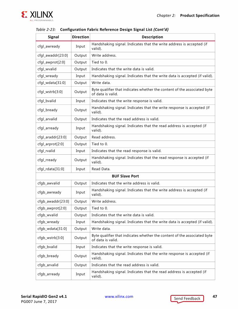
Serial RapidIO Gen2 v4.1 www.xilinx.com 47PG007 June 7, 2017
Chapter 2: Product Specification
cfgl_awready Input Handshaking signal. Indicates that the write address is accepted (if valid).
cfgl_awaddr[23:0] Output Write address.
cfgl_awprot[2:0] Output Tied to 0.
cfgl_wvalid Output Indicates that the write data is valid.
cfgl_wready Input Handshaking signal. Indicates that the write data is accepted (if valid).
cfgl_wdata[31:0] Output Write data.
cfgl_wstrb[3:0] Output Byte qualifier that indicates whether the content of the associated byte of data is valid.
cfgl_bvalid Input Indicates that the write response is valid.
cfgl_bready Output Handshaking signal. Indicates that the write response is accepted (if valid).
cfgl_arvalid Output Indicates that the read address is valid.
cfgl_arready Input Handshaking signal. Indicates that the read address is accepted (if valid).
cfgl_araddr[23:0] Output Read address.
cfgl_arprot[2:0] Output Tied to 0.
cfgl_rvalid Input Indicates that the read response is valid.
cfgl_rready Output Handshaking signal. Indicates that the read response is accepted (if valid).
cfgl_rdata[31:0] Input Read Data.
BUF Slave Port
cfgb_awvalid Output Indicates that the write address is valid.
cfgb_awready Input Handshaking signal. Indicates that the write address is accepted (if valid).
cfgb_awaddr[23:0] Output Write address.
cfgb_awprot[2:0] Output Tied to 0.
cfgb_wvalid Output Indicates that the write data is valid.
cfgb_wready Input Handshaking signal. Indicates that the write data is accepted (if valid).
cfgb_wdata[31:0] Output Write data.
cfgb_wstrb[3:0] Output Byte qualifier that indicates whether the content of the associated byte of data is valid.
cfgb_bvalid Input Indicates that the write response is valid.
cfgb_bready Output Handshaking signal. Indicates that the write response is accepted (if valid).
cfgb_arvalid Output Indicates that the read address is valid.
cfgb_arready Input Handshaking signal. Indicates that the read address is accepted (if valid).
Table 2-23: Configuration Fabric Reference Design Signal List (Cont’d)
Signal Direction Description
Send Feedback
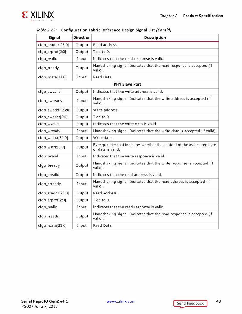
Serial RapidIO Gen2 v4.1 www.xilinx.com 48PG007 June 7, 2017
Chapter 2: Product Specification
cfgb_araddr[23:0] Output Read address.
cfgb_arprot[2:0] Output Tied to 0.
cfgb_rvalid Input Indicates that the read response is valid.
cfgb_rready Output Handshaking signal. Indicates that the read response is accepted (if valid).
cfgb_rdata[31:0] Input Read Data.
PHY Slave Port
cfgp_awvalid Output Indicates that the write address is valid.
cfgp_awready Input Handshaking signal. Indicates that the write address is accepted (if valid).
cfgp_awaddr[23:0] Output Write address.
cfgp_awprot[2:0] Output Tied to 0.
cfgp_wvalid Output Indicates that the write data is valid.
cfgp_wready Input Handshaking signal. Indicates that the write data is accepted (if valid).
cfgp_wdata[31:0] Output Write data.
cfgp_wstrb[3:0] Output Byte qualifier that indicates whether the content of the associated byte of data is valid.
cfgp_bvalid Input Indicates that the write response is valid.
cfgp_bready Output Handshaking signal. Indicates that the write response is accepted (if valid).
cfgp_arvalid Output Indicates that the read address is valid.
cfgp_arready Input Handshaking signal. Indicates that the read address is accepted (if valid).
cfgp_araddr[23:0] Output Read address.
cfgp_arprot[2:0] Output Tied to 0.
cfgp_rvalid Input Indicates that the read response is valid.
cfgp_rready Output Handshaking signal. Indicates that the read response is accepted (if valid).
cfgp_rdata[31:0] Input Read Data.
Table 2-23: Configuration Fabric Reference Design Signal List (Cont’d)
Signal Direction Description
Send Feedback
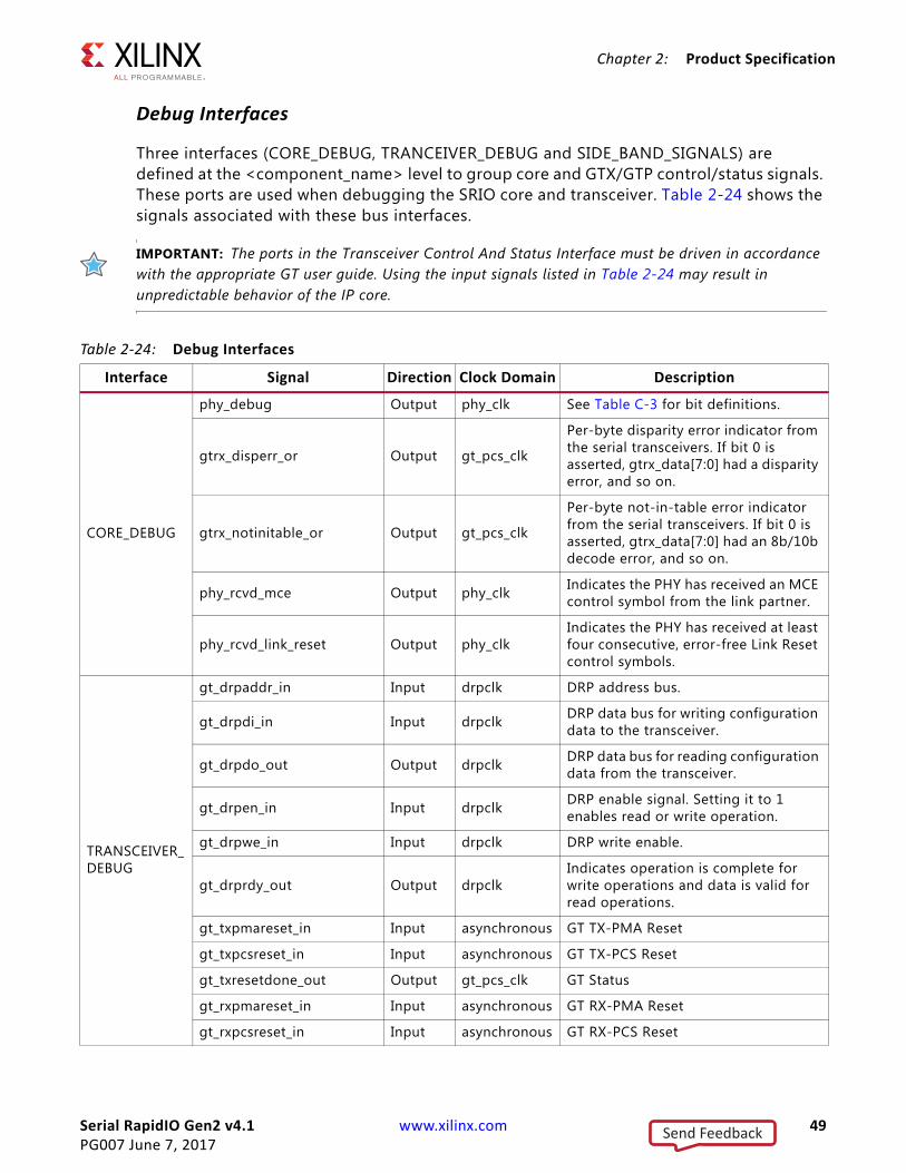
Serial RapidIO Gen2 v4.1 www.xilinx.com 49PG007 June 7, 2017
Chapter 2: Product Specification
Debug Interfaces
Three interfaces (CORE_DEBUG, TRANCEIVER_DEBUG and SIDE_BAND_SIGNALS) are defined at the <component_name> level to group core and GTX/GTP control/status signals. These ports are used when debugging the SRIO core and transceiver. Table 2-24 shows the signals associated with these bus interfaces.
IMPORTANT: The ports in the Transceiver Control And Status Interface must be driven in accordance with the appropriate GT user guide. Using the input signals listed in Table 2-24 may result in unpredictable behavior of the IP core.
Table 2-24: Debug Interfaces
Interface Signal Direction Clock Domain Description
CORE_DEBUG
phy_debug Output phy_clk See Table C-3 for bit definitions.
gtrx_disperr_or Output gt_pcs_clk
Per-byte disparity error indicator from the serial transceivers. If bit 0 is asserted, gtrx_data[7:0] had a disparity error, and so on.
gtrx_notinitable_or Output gt_pcs_clk
Per-byte not-in-table error indicator from the serial transceivers. If bit 0 is asserted, gtrx_data[7:0] had an 8b/10b decode error, and so on.
phy_rcvd_mce Output phy_clk Indicates the PHY has received an MCE control symbol from the link partner.
phy_rcvd_link_reset Output phy_clkIndicates the PHY has received at least four consecutive, error-free Link Reset control symbols.
TRANSCEIVER_DEBUG
gt_drpaddr_in Input drpclk DRP address bus.
gt_drpdi_in Input drpclk DRP data bus for writing configuration data to the transceiver.
gt_drpdo_out Output drpclk DRP data bus for reading configuration data from the transceiver.
gt_drpen_in Input drpclk DRP enable signal. Setting it to 1 enables read or write operation.
gt_drpwe_in Input drpclk DRP write enable.
gt_drprdy_out Output drpclkIndicates operation is complete for write operations and data is valid for read operations.
gt_txpmareset_in Input asynchronous GT TX-PMA Reset
gt_txpcsreset_in Input asynchronous GT TX-PCS Reset
gt_txresetdone_out Output gt_pcs_clk GT Status
gt_rxpmareset_in Input asynchronous GT RX-PMA Reset
gt_rxpcsreset_in Input asynchronous GT RX-PCS Reset
Send Feedback
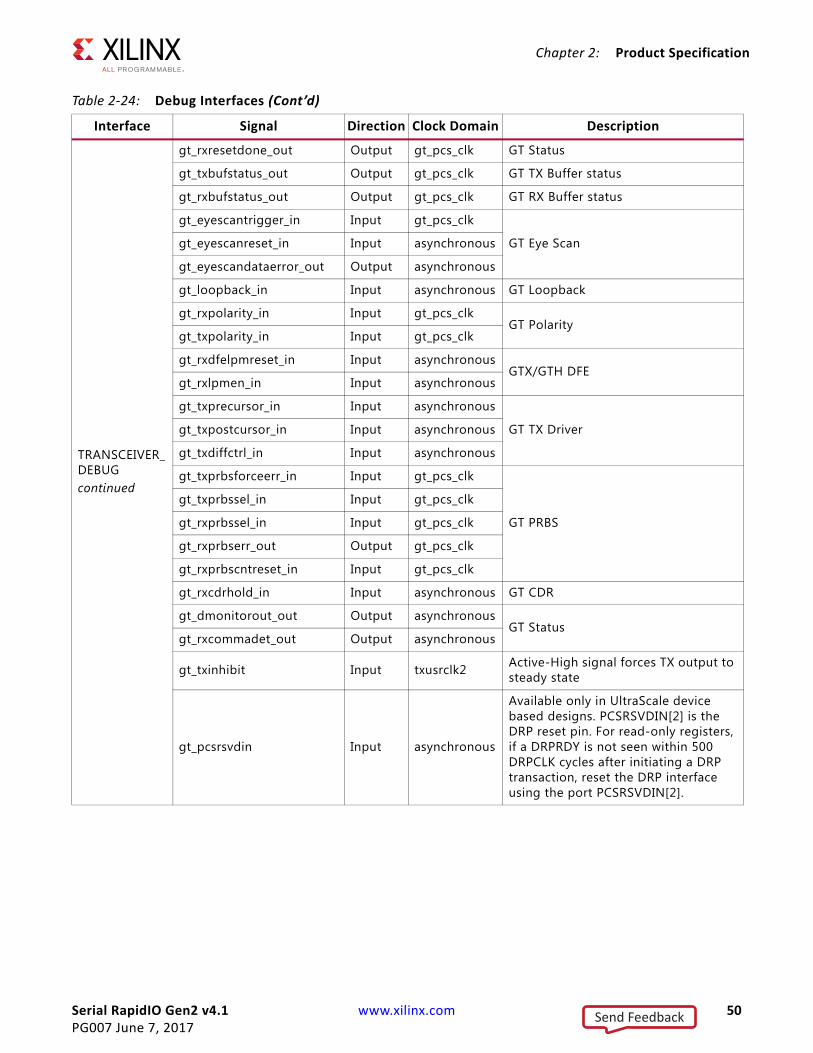
Serial RapidIO Gen2 v4.1 www.xilinx.com 50PG007 June 7, 2017
Chapter 2: Product Specification
TRANSCEIVER_DEBUGcontinued
gt_rxresetdone_out Output gt_pcs_clk GT Status
gt_txbufstatus_out Output gt_pcs_clk GT TX Buffer status
gt_rxbufstatus_out Output gt_pcs_clk GT RX Buffer status
gt_eyescantrigger_in Input gt_pcs_clk
GT Eye Scangt_eyescanreset_in Input asynchronous
gt_eyescandataerror_out Output asynchronous
gt_loopback_in Input asynchronous GT Loopback
gt_rxpolarity_in Input gt_pcs_clkGT Polarity
gt_txpolarity_in Input gt_pcs_clk
gt_rxdfelpmreset_in Input asynchronousGTX/GTH DFE
gt_rxlpmen_in Input asynchronous
gt_txprecursor_in Input asynchronous
GT TX Drivergt_txpostcursor_in Input asynchronous
gt_txdiffctrl_in Input asynchronous
gt_txprbsforceerr_in Input gt_pcs_clk
GT PRBS
gt_txprbssel_in Input gt_pcs_clk
gt_rxprbssel_in Input gt_pcs_clk
gt_rxprbserr_out Output gt_pcs_clk
gt_rxprbscntreset_in Input gt_pcs_clk
gt_rxcdrhold_in Input asynchronous GT CDR
gt_dmonitorout_out Output asynchronousGT Status
gt_rxcommadet_out Output asynchronous
gt_txinhibit Input txusrclk2 Active-High signal forces TX output to steady state
gt_pcsrsvdin Input asynchronous
Available only in UltraScale device based designs. PCSRSVDIN[2] is the DRP reset pin. For read-only registers, if a DRPRDY is not seen within 500 DRPCLK cycles after initiating a DRP transaction, reset the DRP interface using the port PCSRSVDIN[2].
Table 2-24: Debug Interfaces (Cont’d)
Interface Signal Direction Clock Domain Description
Send Feedback
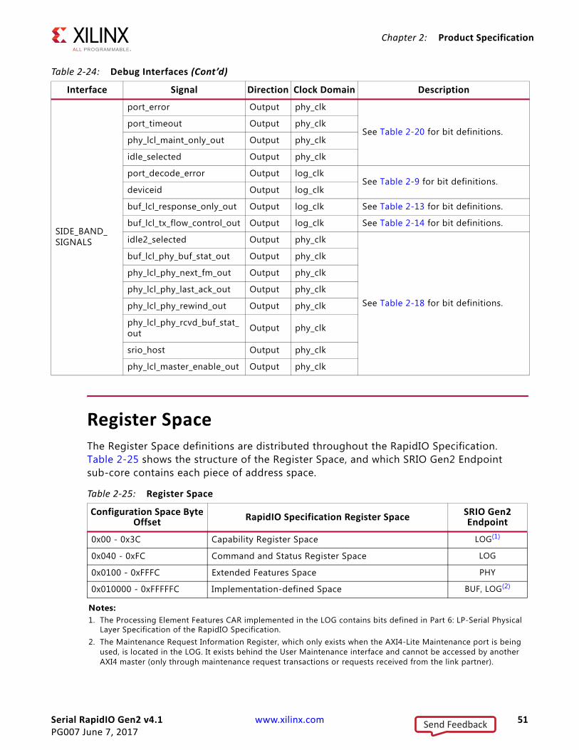
Serial RapidIO Gen2 v4.1 www.xilinx.com 51PG007 June 7, 2017
Chapter 2: Product Specification
Register SpaceThe Register Space definitions are distributed throughout the RapidIO Specification. Table 2-25 shows the structure of the Register Space, and which SRIO Gen2 Endpoint sub-core contains each piece of address space.
SIDE_BAND_SIGNALS
port_error Output phy_clk
See Table 2-20 for bit definitions.port_timeout Output phy_clk
phy_lcl_maint_only_out Output phy_clk
idle_selected Output phy_clk
port_decode_error Output log_clkSee Table 2-9 for bit definitions.
deviceid Output log_clk
buf_lcl_response_only_out Output log_clk See Table 2-13 for bit definitions.
buf_lcl_tx_flow_control_out Output log_clk See Table 2-14 for bit definitions.
idle2_selected Output phy_clk
See Table 2-18 for bit definitions.
buf_lcl_phy_buf_stat_out Output phy_clk
phy_lcl_phy_next_fm_out Output phy_clk
phy_lcl_phy_last_ack_out Output phy_clk
phy_lcl_phy_rewind_out Output phy_clk
phy_lcl_phy_rcvd_buf_stat_out Output phy_clk
srio_host Output phy_clk
phy_lcl_master_enable_out Output phy_clk
Table 2-24: Debug Interfaces (Cont’d)
Interface Signal Direction Clock Domain Description
Table 2-25: Register Space
Configuration Space Byte Offset RapidIO Specification Register Space SRIO Gen2
Endpoint
0x00 - 0x3C Capability Register Space LOG(1)
0x040 - 0xFC Command and Status Register Space LOG
0x0100 - 0xFFFC Extended Features Space PHY
0x010000 - 0xFFFFFC Implementation-defined Space BUF, LOG(2)
Notes: 1. The Processing Element Features CAR implemented in the LOG contains bits defined in Part 6: LP-Serial Physical
Layer Specification of the RapidIO Specification.2. The Maintenance Request Information Register, which only exists when the AXI4-Lite Maintenance port is being
used, is located in the LOG. It exists behind the User Maintenance interface and cannot be accessed by another AXI4 master (only through maintenance request transactions or requests received from the link partner).
Send Feedback
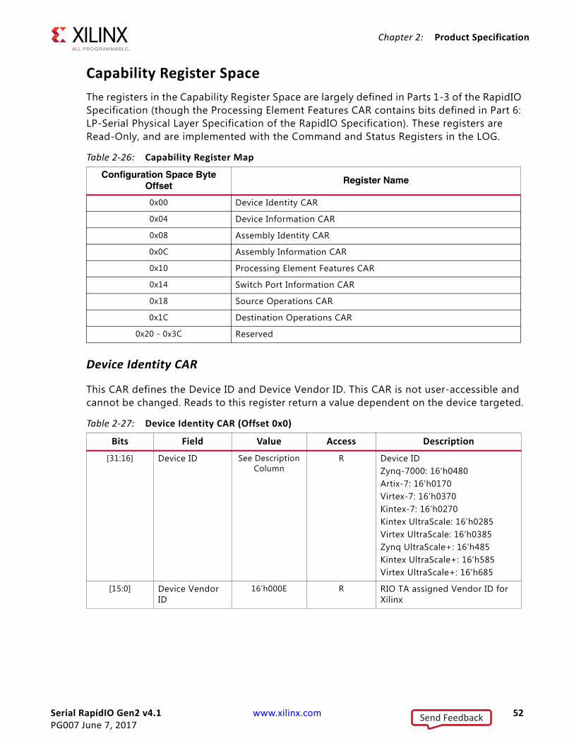
Serial RapidIO Gen2 v4.1 www.xilinx.com 52PG007 June 7, 2017
Chapter 2: Product Specification
Capability Register SpaceThe registers in the Capability Register Space are largely defined in Parts 1-3 of the RapidIO Specification (though the Processing Element Features CAR contains bits defined in Part 6: LP-Serial Physical Layer Specification of the RapidIO Specification). These registers are Read-Only, and are implemented with the Command and Status Registers in the LOG.
Device Identity CAR
This CAR defines the Device ID and Device Vendor ID. This CAR is not user-accessible and cannot be changed. Reads to this register return a value dependent on the device targeted.
Table 2-26: Capability Register Map
Configuration Space Byte Offset
Register Name
0x00 Device Identity CAR
0x04 Device Information CAR
0x08 Assembly Identity CAR
0x0C Assembly Information CAR
0x10 Processing Element Features CAR
0x14 Switch Port Information CAR
0x18 Source Operations CAR
0x1C Destination Operations CAR
0x20 - 0x3C Reserved
Table 2-27: Device Identity CAR (Offset 0x0)
Bits Field Value Access Description
[31:16] Device ID See Description Column
R Device IDZynq-7000: 16'h0480Artix-7: 16'h0170Virtex-7: 16’h0370Kintex-7: 16’h0270Kintex UltraScale: 16’h0285Virtex UltraScale: 16’h0385Zynq UltraScale+: 16'h485Kintex UltraScale+: 16'h585Virtex UltraScale+: 16'h685
[15:0] Device Vendor ID
16’h000E R RIO TA assigned Vendor ID for Xilinx
Send Feedback
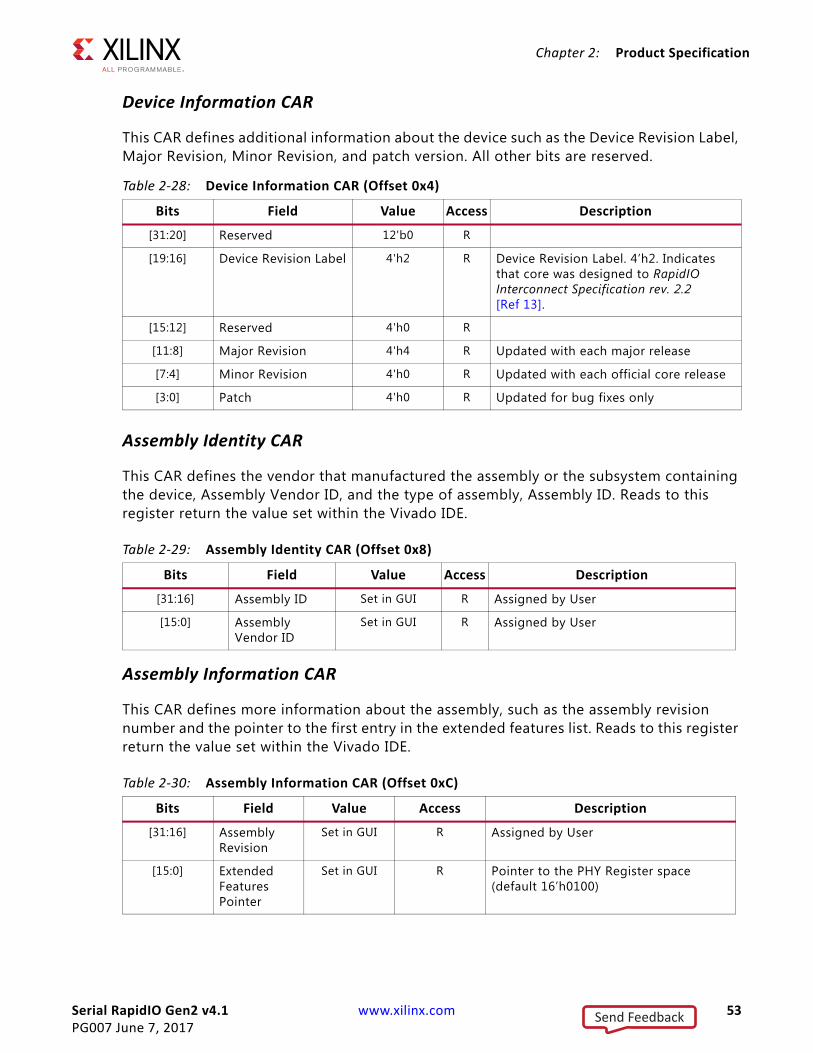
Serial RapidIO Gen2 v4.1 www.xilinx.com 53PG007 June 7, 2017
Chapter 2: Product Specification
Device Information CAR
This CAR defines additional information about the device such as the Device Revision Label, Major Revision, Minor Revision, and patch version. All other bits are reserved.
Assembly Identity CAR
This CAR defines the vendor that manufactured the assembly or the subsystem containing the device, Assembly Vendor ID, and the type of assembly, Assembly ID. Reads to this register return the value set within the Vivado IDE.
Assembly Information CAR
This CAR defines more information about the assembly, such as the assembly revision number and the pointer to the first entry in the extended features list. Reads to this register return the value set within the Vivado IDE.
Table 2-28: Device Information CAR (Offset 0x4)
Bits Field Value Access Description
[31:20] Reserved 12'b0 R
[19:16] Device Revision Label 4'h2 R Device Revision Label. 4’h2. Indicates that core was designed to RapidIO Interconnect Specification rev. 2.2 [Ref 13].
[15:12] Reserved 4'h0 R
[11:8] Major Revision 4'h4 R Updated with each major release
[7:4] Minor Revision 4'h0 R Updated with each official core release
[3:0] Patch 4'h0 R Updated for bug fixes only
Table 2-29: Assembly Identity CAR (Offset 0x8)
Bits Field Value Access Description
[31:16] Assembly ID Set in GUI R Assigned by User
[15:0] Assembly Vendor ID
Set in GUI R Assigned by User
Table 2-30: Assembly Information CAR (Offset 0xC)
Bits Field Value Access Description
[31:16] Assembly Revision
Set in GUI R Assigned by User
[15:0] Extended Features Pointer
Set in GUI R Pointer to the PHY Register space (default 16’h0100)
Send Feedback
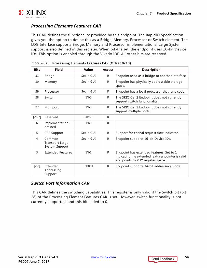
Serial RapidIO Gen2 v4.1 www.xilinx.com 54PG007 June 7, 2017
Chapter 2: Product Specification
Processing Elements Features CAR
This CAR defines the functionality provided by this endpoint. The RapidIO Specification gives you the option to define this as a Bridge, Memory, Processor or Switch element. The LOG Interface supports Bridge, Memory and Processor implementations. Large System support is also defined in this register. When bit 4 is set, the endpoint uses 16-bit Device IDs. This option is enabled through the Vivado IDE. All other bits are reserved.
Switch Port Information CAR
This CAR defines the switching capabilities. This register is only valid if the Switch bit (bit 28) of the Processing Element Features CAR is set. However, switch functionality is not currently supported, and this bit is tied to 0.
Table 2-31: Processing Elements Features CAR (Offset 0x10)
Bits Field Value Access Description
31 Bridge Set in GUI R Endpoint used as a bridge to another interface.
30 Memory Set in GUI R Endpoint has physically addressable storage space.
29 Processor Set in GUI R Endpoint has a local processor that runs code.
28 Switch 1'b0 R The SRIO Gen2 Endpoint does not currently support switch functionality.
27 Multiport 1'b0 R The SRIO Gen2 Endpoint does not currently support multiple ports.
[26:7] Reserved 20'b0 R
6 Implementation-defined
1'b0 R
5 CRF Support Set in GUI R Support for critical request flow indicator.
4 Common Transport Large System Support
Set in GUI R Endpoint supports 16-bit Device IDs.
3 Extended Features 1'b1 R Endpoint has extended features. Set to 1 indicating the extended features pointer is valid and points to PHY register space.
[2:0] Extended Addressing Support
3'b001 R Endpoint supports 34-bit addressing mode.
Send Feedback
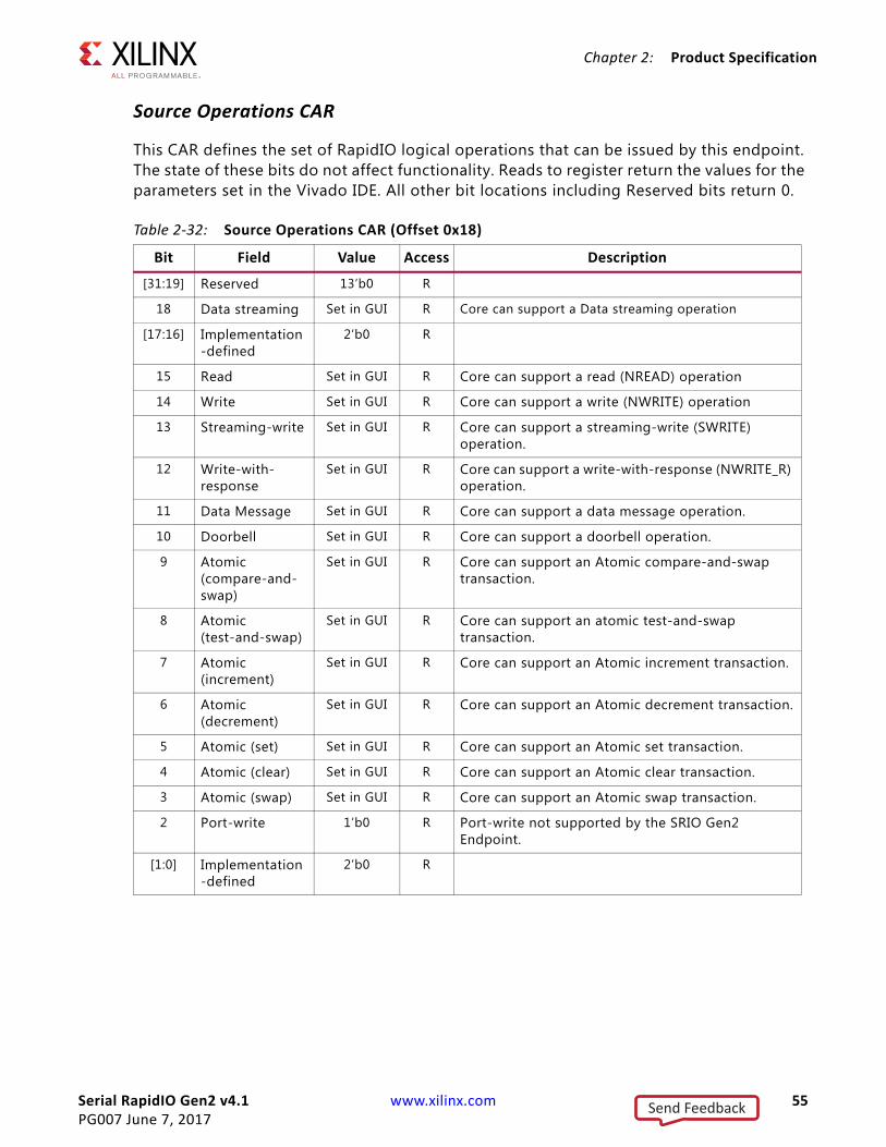
Serial RapidIO Gen2 v4.1 www.xilinx.com 55PG007 June 7, 2017
Chapter 2: Product Specification
Source Operations CAR
This CAR defines the set of RapidIO logical operations that can be issued by this endpoint. The state of these bits do not affect functionality. Reads to register return the values for the parameters set in the Vivado IDE. All other bit locations including Reserved bits return 0.
Table 2-32: Source Operations CAR (Offset 0x18)
Bit Field Value Access Description
[31:19] Reserved 13’b0 R
18 Data streaming Set in GUI R Core can support a Data streaming operation
[17:16] Implementation-defined
2’b0 R
15 Read Set in GUI R Core can support a read (NREAD) operation
14 Write Set in GUI R Core can support a write (NWRITE) operation
13 Streaming-write Set in GUI R Core can support a streaming-write (SWRITE) operation.
12 Write-with-response
Set in GUI R Core can support a write-with-response (NWRITE_R) operation.
11 Data Message Set in GUI R Core can support a data message operation.
10 Doorbell Set in GUI R Core can support a doorbell operation.
9 Atomic (compare-and-swap)
Set in GUI R Core can support an Atomic compare-and-swap transaction.
8 Atomic (test-and-swap)
Set in GUI R Core can support an atomic test-and-swap transaction.
7 Atomic (increment)
Set in GUI R Core can support an Atomic increment transaction.
6 Atomic (decrement)
Set in GUI R Core can support an Atomic decrement transaction.
5 Atomic (set) Set in GUI R Core can support an Atomic set transaction.
4 Atomic (clear) Set in GUI R Core can support an Atomic clear transaction.
3 Atomic (swap) Set in GUI R Core can support an Atomic swap transaction.
2 Port-write 1’b0 R Port-write not supported by the SRIO Gen2 Endpoint.
[1:0] Implementation-defined
2’b0 R
Send Feedback

Serial RapidIO Gen2 v4.1 www.xilinx.com 56PG007 June 7, 2017
Chapter 2: Product Specification
Destination Operations CAR
This CAR defines the set of RapidIO logical operations that can be supported by this endpoint. Reads to register return the values for the parameters set in the Vivado IDE. All other bit locations including Reserved bits returns 0.
Table 2-33: Destination Operations CAR (Offset 0x1C)
Bit Field Name Value Access Description
[31:19] Reserved 13’b0 R
18 Data streaming Set in GUI R Core can support a Data streaming operation
[17:16] Implementation-defined 2’b0 R
15 Read Set in GUI R Core can support a read (NREAD) operation.
14 Write Set in GUI R Core can support a write (NWRITE) operation.
13 Streaming-write Set in GUI R Core can support a streaming-write (SWRITE) operation.
12 Write-with-response Set in GUI R Core can support a write-with-response (NWRITE_R) operation.
11 Data message Set in GUI R Core can support a data message operation.
10 Doorbell Set in GUI R Core can support a doorbell operation.
9 Atomic (compare-and-swap) Set in GUI R Core can support an Atomic compare-and-swap transaction.
8 Atomic (test-and-swap) Set in GUI R Core can support an atomic test-and-swap transaction.
7 Atomic (increment) Set in GUI R Core can support an Atomic increment transaction.
6 Atomic (decrement) Set in GUI R Core can support an Atomic decrement transaction.
5 Atomic (set) Set in GUI R Core can support an Atomic set transaction.
4 Atomic (clear) Set in GUI R Core can support an Atomic clear transaction.
3 Atomic (swap) Set in GUI R Core can support an Atomic swap transaction.
2 Port-write 1’b0 R Port-write not supported by the SRIO Gen2 Endpoint.
[1:0] Implementation-defined 2’b0 R
Send Feedback
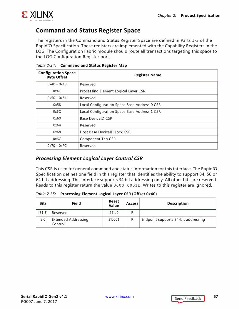
Serial RapidIO Gen2 v4.1 www.xilinx.com 57PG007 June 7, 2017
Chapter 2: Product Specification
Command and Status Register SpaceThe registers in the Command and Status Register Space are defined in Parts 1-3 of the RapidIO Specification. These registers are implemented with the Capability Registers in the LOG. The Configuration Fabric module should route all transactions targeting this space to the LOG Configuration Register port.
Processing Element Logical Layer Control CSR
This CSR is used for general command and status information for this interface. The RapidIO Specification defines one field in this register that identifies the ability to support 34, 50 or 64 bit addressing. This interface supports 34 bit addressing only. All other bits are reserved. Reads to this register return the value 0000_0001h. Writes to this register are ignored.
Table 2-34: Command and Status Register Map
Configuration Space Byte Offset Register Name
0x40 - 0x48 Reserved
0x4C Processing Element Logical Layer CSR
0x50 - 0x54 Reserved
0x58 Local Configuration Space Base Address 0 CSR
0x5C Local Configuration Space Base Address 1 CSR
0x60 Base DeviceID CSR
0x64 Reserved
0x68 Host Base DeviceID Lock CSR
0x6C Component Tag CSR
0x70 - 0xFC Reserved
Table 2-35: Processing Element Logical Layer CSR (Offset 0x4C)
Bits Field Reset Value Access Description
[31:3] Reserved 29'b0 R
[2:0] Extended Addressing Control
3'b001 R Endpoint supports 34-bit addressing
Send Feedback
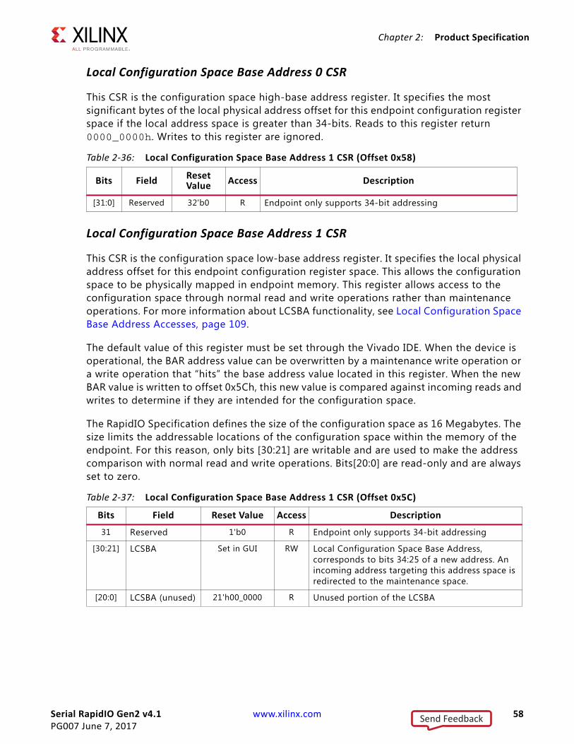
Serial RapidIO Gen2 v4.1 www.xilinx.com 58PG007 June 7, 2017
Chapter 2: Product Specification
Local Configuration Space Base Address 0 CSR
This CSR is the configuration space high-base address register. It specifies the most significant bytes of the local physical address offset for this endpoint configuration register space if the local address space is greater than 34-bits. Reads to this register return 0000_0000h. Writes to this register are ignored.
Local Configuration Space Base Address 1 CSR
This CSR is the configuration space low-base address register. It specifies the local physical address offset for this endpoint configuration register space. This allows the configuration space to be physically mapped in endpoint memory. This register allows access to the configuration space through normal read and write operations rather than maintenance operations. For more information about LCSBA functionality, see Local Configuration Space Base Address Accesses, page 109.
The default value of this register must be set through the Vivado IDE. When the device is operational, the BAR address value can be overwritten by a maintenance write operation or a write operation that “hits” the base address value located in this register. When the new BAR value is written to offset 0x5Ch, this new value is compared against incoming reads and writes to determine if they are intended for the configuration space.
The RapidIO Specification defines the size of the configuration space as 16 Megabytes. The size limits the addressable locations of the configuration space within the memory of the endpoint. For this reason, only bits [30:21] are writable and are used to make the address comparison with normal read and write operations. Bits[20:0] are read-only and are always set to zero.
Table 2-36: Local Configuration Space Base Address 1 CSR (Offset 0x58)
Bits Field Reset Value Access Description
[31:0] Reserved 32'b0 R Endpoint only supports 34-bit addressing
Table 2-37: Local Configuration Space Base Address 1 CSR (Offset 0x5C)
Bits Field Reset Value Access Description
31 Reserved 1'b0 R Endpoint only supports 34-bit addressing
[30:21] LCSBA Set in GUI RW Local Configuration Space Base Address, corresponds to bits 34:25 of a new address. An incoming address targeting this address space is redirected to the maintenance space.
[20:0] LCSBA (unused) 21'h00_0000 R Unused portion of the LCSBA
Send Feedback

Serial RapidIO Gen2 v4.1 www.xilinx.com 59PG007 June 7, 2017
Chapter 2: Product Specification
Base Device ID CSR
This CSR contains the base Device ID value for this endpoint. For 8-bit Device ID, bits [23:16] are valid. If Large System Support is enabled, then the 16-bit Device ID occupies bits [15:0]. The default value of this register must be set through the Vivado IDE. All other bits are reserved. Reads to reserved bits return 0 and writes are ignored.
Host Base Device ID Lock CSR
This CSR contains the base Device ID value for the Host that is responsible for initializing this endpoint. This register is a write-once register which provides a lock function. Reads after reset return a default value of 0000_FFFFh. This register can be written once after reset. All subsequent writes are ignored except when bits [15:0] of the written value matches the value contained in the register field (both bytes must be written simultaneously for the comparison to occur), in which case they are reset to 0000_FFFFh. Writes of 16’hFFFF to the Host_base_deviceID field do not lock the CSR.
Component Tag CSR
This CSR contains a component tag value for this endpoint and can be assigned by software during initialization. Reads after reset return a default value of 0000_0000h. The value can be changed through a maintenance write operation or a normal write operation with the configuration space base address offset 0x6C.
Table 2-38: Base DeviceID CSR (Offset 0x60)
Bits Field Reset Value Access Description
[31:24] Reserved 8'h00 R
[23:16] Base_deviceID Set in GUI RW 8-bit Device ID for an endpoint in a small transport system
[15:0] Large_base_deviceID Set in GUI RW 16-bit Device ID for an endpoint in a large transport system
Table 2-39: Host Base Device ID Lock CSR (Offset 0x68)
Bits Field Reset Value Access Description
[31:16] Reserved 16'h0000 R
[15:0] Host_base_deviceID 16'hFFFF RW once
Device ID of the system host. The field is writable when value is 16'hFFFF. Otherwise writing the current value resets to 16'hFFFF to allow for a host base Device ID change.
Table 2-40: Component Tag CSR (Offset 0x6C)
Bits Field Reset Value Access Description
[31:0] Component_Tag 32'h0000_0000 RW Component Tag to be set by software at initialization.
Send Feedback
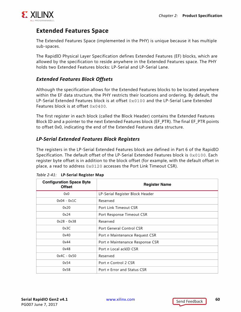
Serial RapidIO Gen2 v4.1 www.xilinx.com 60PG007 June 7, 2017
Chapter 2: Product Specification
Extended Features SpaceThe Extended Features Space (implemented in the PHY) is unique because it has multiple sub-spaces.
The RapidIO Physical Layer Specification defines Extended Features (EF) blocks, which are allowed by the specification to reside anywhere in the Extended Features space. The PHY holds two Extended Features blocks: LP-Serial and LP-Serial Lane.
Extended Features Block Offsets
Although the specification allows for the Extended Features blocks to be located anywhere within the EF data structure, the PHY restricts their locations and ordering. By default, the LP-Serial Extended Features block is at offset 0x0100 and the LP-Serial Lane Extended Features block is at offset 0x0400.
The first register in each block (called the Block Header) contains the Extended Features Block ID and a pointer to the next Extended Features block (EF_PTR). The final EF_PTR points to offset 0x0, indicating the end of the Extended Features data structure.
LP-Serial Extended Features Block Registers
The registers in the LP-Serial Extended Features block are defined in Part 6 of the RapidIO Specification. The default offset of the LP-Serial Extended Features block is 0x0100. Each register byte offset is in addition to the block offset (for example, with the default offset in place, a read to address 0x0120 accesses the Port Link Timeout CSR).
Table 2-41: LP-Serial Register Map
Configuration Space Byte Offset
Register Name
0x0 LP-Serial Register Block Header
0x04 - 0x1C Reserved
0x20 Port Link Timeout CSR
0x24 Port Response Timeout CSR
0x28 - 0x38 Reserved
0x3C Port General Control CSR
0x40 Port n Maintenance Request CSR
0x44 Port n Maintenance Response CSR
0x48 Port n Local ackID CSR
0x4C - 0x50 Reserved
0x54 Port n Control 2 CSR
0x58 Port n Error and Status CSR
Send Feedback
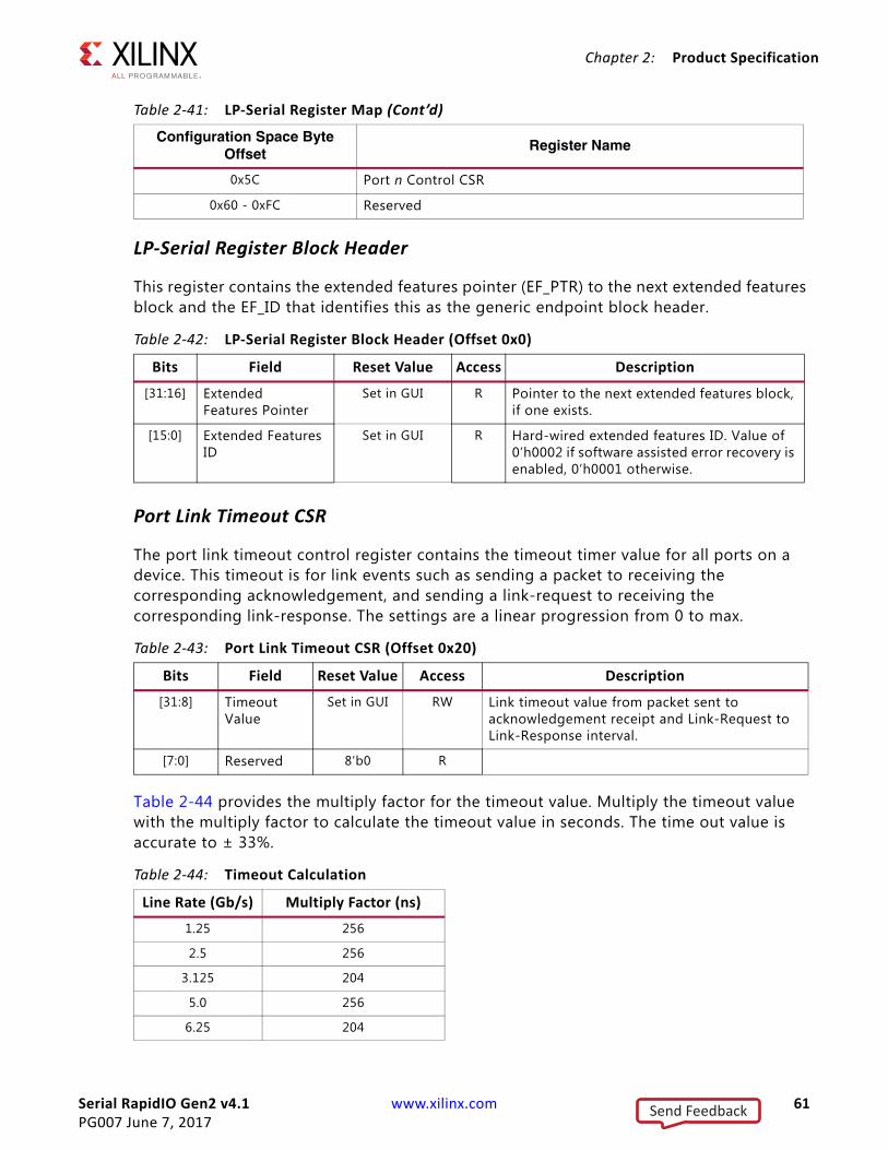
Serial RapidIO Gen2 v4.1 www.xilinx.com 61PG007 June 7, 2017
Chapter 2: Product Specification
LP-Serial Register Block Header
This register contains the extended features pointer (EF_PTR) to the next extended features block and the EF_ID that identifies this as the generic endpoint block header.
Port Link Timeout CSR
The port link timeout control register contains the timeout timer value for all ports on a device. This timeout is for link events such as sending a packet to receiving the corresponding acknowledgement, and sending a link-request to receiving the corresponding link-response. The settings are a linear progression from 0 to max.
Table 2-44 provides the multiply factor for the timeout value. Multiply the timeout value with the multiply factor to calculate the timeout value in seconds. The time out value is accurate to ± 33%.
0x5C Port n Control CSR
0x60 - 0xFC Reserved
Table 2-42: LP-Serial Register Block Header (Offset 0x0)
Bits Field Reset Value Access Description
[31:16] Extended Features Pointer
Set in GUI R Pointer to the next extended features block, if one exists.
[15:0] Extended Features ID
Set in GUI R Hard-wired extended features ID. Value of 0’h0002 if software assisted error recovery is enabled, 0’h0001 otherwise.
Table 2-43: Port Link Timeout CSR (Offset 0x20)
Bits Field Reset Value Access Description
[31:8] Timeout Value
Set in GUI RW Link timeout value from packet sent to acknowledgement receipt and Link-Request to Link-Response interval.
[7:0] Reserved 8'b0 R
Table 2-44: Timeout Calculation
Line Rate (Gb/s) Multiply Factor (ns)
1.25 256
2.5 256
3.125 204
5.0 256
6.25 204
Table 2-41: LP-Serial Register Map (Cont’d)
Configuration Space Byte Offset
Register Name
Send Feedback

Serial RapidIO Gen2 v4.1 www.xilinx.com 62PG007 June 7, 2017
Chapter 2: Product Specification
Port Response Timeout CSR
The port response timeout control register contains the timeout timer count for all ports on a device. This timeout is for sending a request packet to receiving the corresponding response packet. Table 2-44 provides the multiply factor for the timeout value. Multiply the timeout value with the multiply factor to calculate the timeout value in seconds.
Port General Control CSR
The bits accessible through this CSR apply to all ports on a device. There is a single copy of each such bit per device.
Port n Link Maintenance Request CSR
A write to this register generates a link-request control symbol on the corresponding port. This register is available only if the software assisted error recovery option is selected in the Vivado IDE.
Table 2-45: Port Response Timeout CSR (Offset 0x24)
Bits Field Reset Value Access Description
[31:8] Timeout Value Set in GUI RW Timeout from sending a Request packet to receiving a response packet.
[7:0] Reserved 8'b0 R
Table 2-46: Port General Control CSR (Offset 0x3C)
Bits Field Reset Value Access Description
31 Host Set in GUI RW Device responsible for system exploration.
30 Master Enable
Set in GUI RW Device is allowed to issue requests into the system. If set to 0, the core does not accept requests from the user design.
29 Discovered Set in GUI RW Device has been located by the PE responsible for system exploration.
[28:0] Reserved 29'b0 R
Table 2-47: Port n Link Maintenance Request CSR (Offset 0x40)
Bits Field ResetValue Access Description
[31:3] Reserved 29’b0 R
[2:0] Command 3’b0 RW Command that is sent in the link-request control symbol.
Send Feedback
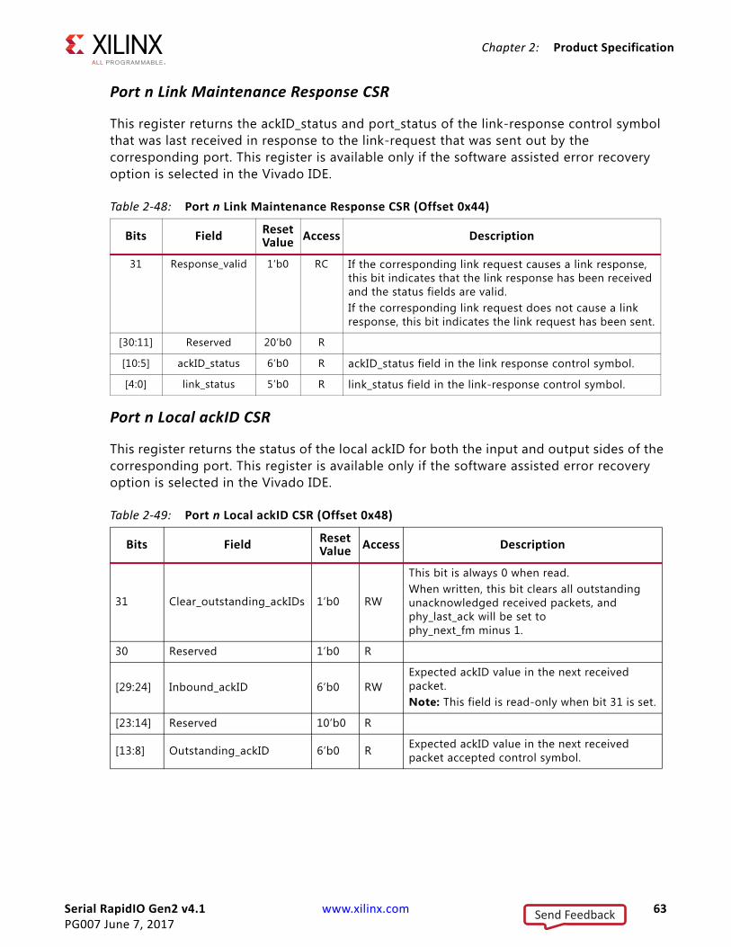
Serial RapidIO Gen2 v4.1 www.xilinx.com 63PG007 June 7, 2017
Chapter 2: Product Specification
Port n Link Maintenance Response CSR
This register returns the ackID_status and port_status of the link-response control symbol that was last received in response to the link-request that was sent out by the corresponding port. This register is available only if the software assisted error recovery option is selected in the Vivado IDE.
Port n Local ackID CSR
This register returns the status of the local ackID for both the input and output sides of the corresponding port. This register is available only if the software assisted error recovery option is selected in the Vivado IDE.
Table 2-48: Port n Link Maintenance Response CSR (Offset 0x44)
Bits Field ResetValue Access Description
31 Response_valid 1’b0 RC If the corresponding link request causes a link response, this bit indicates that the link response has been received and the status fields are valid. If the corresponding link request does not cause a link response, this bit indicates the link request has been sent.
[30:11] Reserved 20’b0 R
[10:5] ackID_status 6’b0 R ackID_status field in the link response control symbol.
[4:0] link_status 5’b0 R link_status field in the link-response control symbol.
Table 2-49: Port n Local ackID CSR (Offset 0x48)
Bits Field ResetValue Access Description
31 Clear_outstanding_ackIDs 1’b0 RW
This bit is always 0 when read.When written, this bit clears all outstanding unacknowledged received packets, and phy_last_ack will be set to phy_next_fm minus 1.
30 Reserved 1’b0 R
[29:24] Inbound_ackID 6’b0 RWExpected ackID value in the next received packet.Note: This field is read-only when bit 31 is set.
[23:14] Reserved 10’b0 R
[13:8] Outstanding_ackID 6’b0 R Expected ackID value in the next received packet accepted control symbol.
Send Feedback
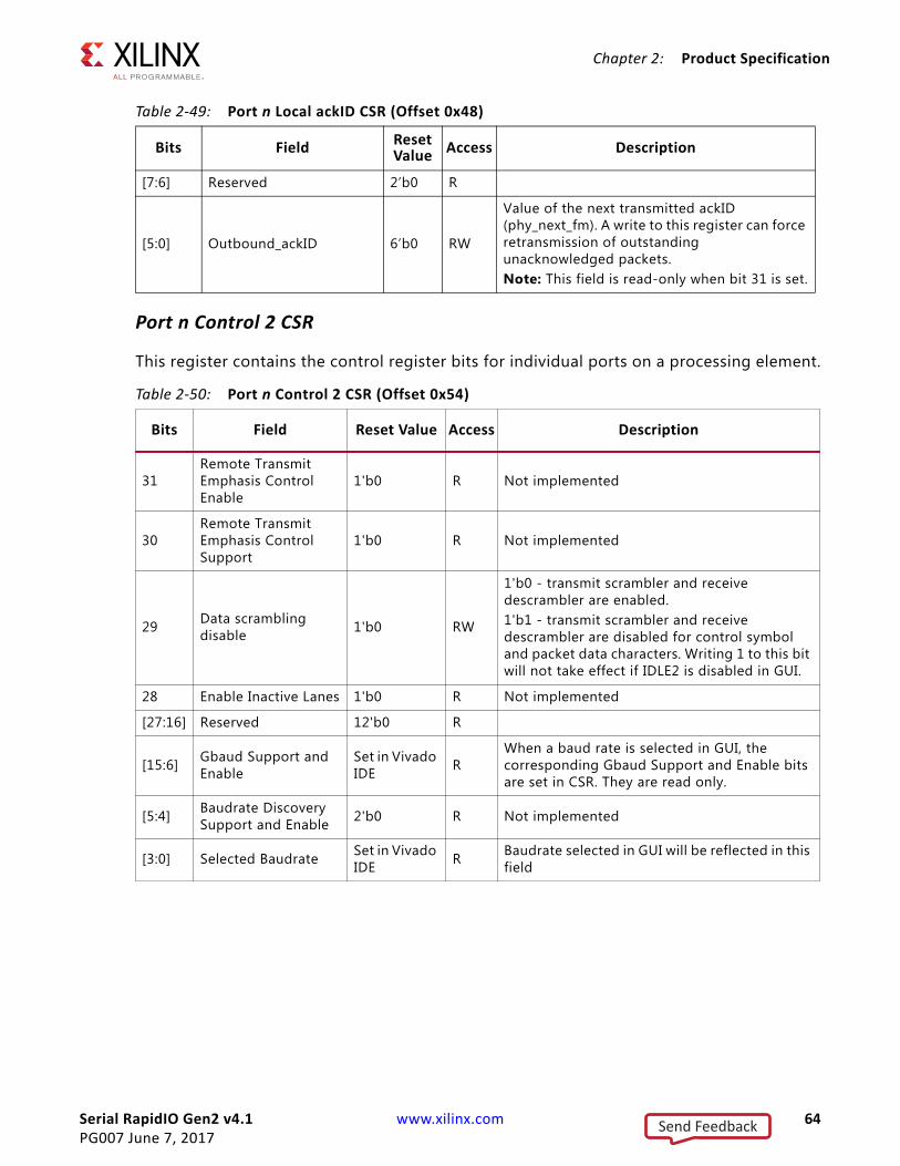
Serial RapidIO Gen2 v4.1 www.xilinx.com 64PG007 June 7, 2017
Chapter 2: Product Specification
Port n Control 2 CSR
This register contains the control register bits for individual ports on a processing element.
[7:6] Reserved 2’b0 R
[5:0] Outbound_ackID 6’b0 RW
Value of the next transmitted ackID (phy_next_fm). A write to this register can force retransmission of outstanding unacknowledged packets.Note: This field is read-only when bit 31 is set.
Table 2-50: Port n Control 2 CSR (Offset 0x54)
Bits Field Reset Value Access Description
31Remote Transmit Emphasis Control Enable
1'b0 R Not implemented
30Remote Transmit Emphasis Control Support
1'b0 R Not implemented
29 Data scrambling disable 1'b0 RW
1'b0 - transmit scrambler and receive descrambler are enabled.1'b1 - transmit scrambler and receive descrambler are disabled for control symbol and packet data characters. Writing 1 to this bit will not take effect if IDLE2 is disabled in GUI.
28 Enable Inactive Lanes 1'b0 R Not implemented
[27:16] Reserved 12'b0 R
[15:6] Gbaud Support and Enable
Set in Vivado IDE R
When a baud rate is selected in GUI, the corresponding Gbaud Support and Enable bits are set in CSR. They are read only.
[5:4] Baudrate Discovery Support and Enable 2'b0 R Not implemented
[3:0] Selected Baudrate Set in Vivado IDE R Baudrate selected in GUI will be reflected in this
field
Table 2-49: Port n Local ackID CSR (Offset 0x48)
Bits Field ResetValue Access Description
Send Feedback
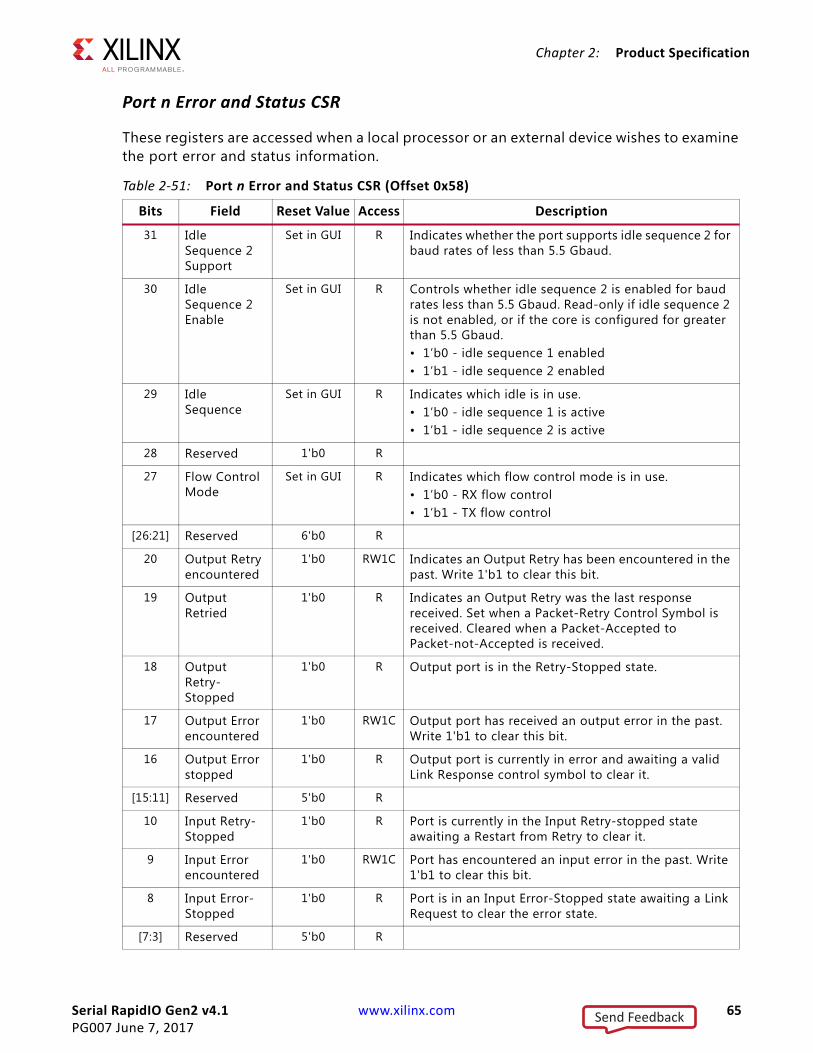
Serial RapidIO Gen2 v4.1 www.xilinx.com 65PG007 June 7, 2017
Chapter 2: Product Specification
Port n Error and Status CSR
These registers are accessed when a local processor or an external device wishes to examine the port error and status information.
Table 2-51: Port n Error and Status CSR (Offset 0x58)
Bits Field Reset Value Access Description
31 Idle Sequence 2 Support
Set in GUI R Indicates whether the port supports idle sequence 2 for baud rates of less than 5.5 Gbaud.
30 Idle Sequence 2 Enable
Set in GUI R Controls whether idle sequence 2 is enabled for baud rates less than 5.5 Gbaud. Read-only if idle sequence 2 is not enabled, or if the core is configured for greater than 5.5 Gbaud.• 1’b0 - idle sequence 1 enabled• 1’b1 - idle sequence 2 enabled
29 Idle Sequence
Set in GUI R Indicates which idle is in use.• 1’b0 - idle sequence 1 is active• 1’b1 - idle sequence 2 is active
28 Reserved 1'b0 R
27 Flow Control Mode
Set in GUI R Indicates which flow control mode is in use.• 1’b0 - RX flow control• 1’b1 - TX flow control
[26:21] Reserved 6'b0 R
20 Output Retry encountered
1'b0 RW1C Indicates an Output Retry has been encountered in the past. Write 1'b1 to clear this bit.
19 Output Retried
1'b0 R Indicates an Output Retry was the last response received. Set when a Packet-Retry Control Symbol is received. Cleared when a Packet-Accepted to Packet-not-Accepted is received.
18 Output Retry-Stopped
1'b0 R Output port is in the Retry-Stopped state.
17 Output Error encountered
1'b0 RW1C Output port has received an output error in the past. Write 1'b1 to clear this bit.
16 Output Error stopped
1'b0 R Output port is currently in error and awaiting a valid Link Response control symbol to clear it.
[15:11] Reserved 5'b0 R
10 Input Retry-Stopped
1'b0 R Port is currently in the Input Retry-stopped state awaiting a Restart from Retry to clear it.
9 Input Error encountered
1'b0 RW1C Port has encountered an input error in the past. Write 1'b1 to clear this bit.
8 Input Error-Stopped
1'b0 R Port is in an Input Error-Stopped state awaiting a Link Request to clear the error state.
[7:3] Reserved 5'b0 R
Send Feedback
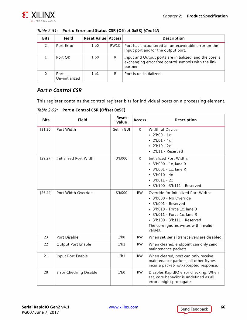
Serial RapidIO Gen2 v4.1 www.xilinx.com 66PG007 June 7, 2017
Chapter 2: Product Specification
Port n Control CSR
This register contains the control register bits for individual ports on a processing element.
2 Port Error 1'b0 RW1C Port has encountered an unrecoverable error on the input port and/or the output port.
1 Port OK 1'b0 R Input and Output ports are initialized, and the core is exchanging error free control symbols with the link partner.
0 Port Un-initialized
1'b1 R Port is un-initialized.
Table 2-52: Port n Control CSR (Offset 0x5C)
Bits Field Reset Value Access Description
[31:30] Port Width Set in GUI R Width of Device:• 2'b00 - 1x• 2'b01 - 4x• 2'b10 - 2x• 2'b11 - Reserved
[29:27] Initialized Port Width 3'b000 R Initialized Port Width:• 3'b000 - 1x, lane 0• 3'b001 - 1x, lane R• 3'b010 - 4x• 3'b011 - 2x• 3'b100 - 3'b111 - Reserved
[26:24] Port Width Override 3'b000 RW Override for Initialized Port Width:• 3'b000 - No Override• 3'b001 - Reserved• 3'b010 - Force 1x, lane 0• 3'b011 - Force 1x, lane R• 3'b100 - 3'b111 - ReservedThe core ignores writes with invalid values.
23 Port Disable 1'b0 RW When set, serial transceivers are disabled.
22 Output Port Enable 1'b1 RW When cleared, endpoint can only send maintenance packets.
21 Input Port Enable 1'b1 RW When cleared, port can only receive maintenance packets, all other ftypes incur a packet-not-accepted response.
20 Error Checking Disable 1'b0 RW Disables RapidIO error checking. When set, core behavior is undefined as all errors might propagate.
Table 2-51: Port n Error and Status CSR (Offset 0x58) (Cont’d)
Bits Field Reset Value Access Description
Send Feedback
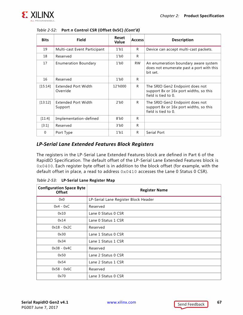
Serial RapidIO Gen2 v4.1 www.xilinx.com 67PG007 June 7, 2017
Chapter 2: Product Specification
LP-Serial Lane Extended Features Block Registers
The registers in the LP-Serial Lane Extended Features block are defined in Part 6 of the RapidIO Specification. The default offset of the LP-Serial Lane Extended Features block is 0x0400. Each register byte offset is in addition to the block offset (for example, with the default offset in place, a read to address 0x0410 accesses the Lane 0 Status 0 CSR).
19 Multi-cast Event Participant 1’b1 R Device can accept multi-cast packets.
18 Reserved 1'b0 R
17 Enumeration Boundary 1'b0 RW An enumeration boundary aware system does not enumerate past a port with this bit set.
16 Reserved 1'b0 R
[15:14] Extended Port Width Override
12'h000 R The SRIO Gen2 Endpoint does not support 8x or 16x port widths, so this field is tied to 0.
[13:12] Extended Port Width Support
2’b0 R The SRIO Gen2 Endpoint does not support 8x or 16x port widths, so this field is tied to 0.
[11:4] Implementation-defined 8’b0 R
[3:1] Reserved 3'b0 R
0 Port Type 1'b1 R Serial Port
Table 2-53: LP-Serial Lane Register Map
Configuration Space Byte Offset Register Name
0x0 LP-Serial Lane Register Block Header
0x4 - 0xC Reserved
0x10 Lane 0 Status 0 CSR
0x14 Lane 0 Status 1 CSR
0x18 - 0x2C Reserved
0x30 Lane 1 Status 0 CSR
0x34 Lane 1 Status 1 CSR
0x38 - 0x4C Reserved
0x50 Lane 2 Status 0 CSR
0x54 Lane 2 Status 1 CSR
0x58 - 0x6C Reserved
0x70 Lane 3 Status 0 CSR
Table 2-52: Port n Control CSR (Offset 0x5C) (Cont’d)
Bits Field Reset Value Access Description
Send Feedback
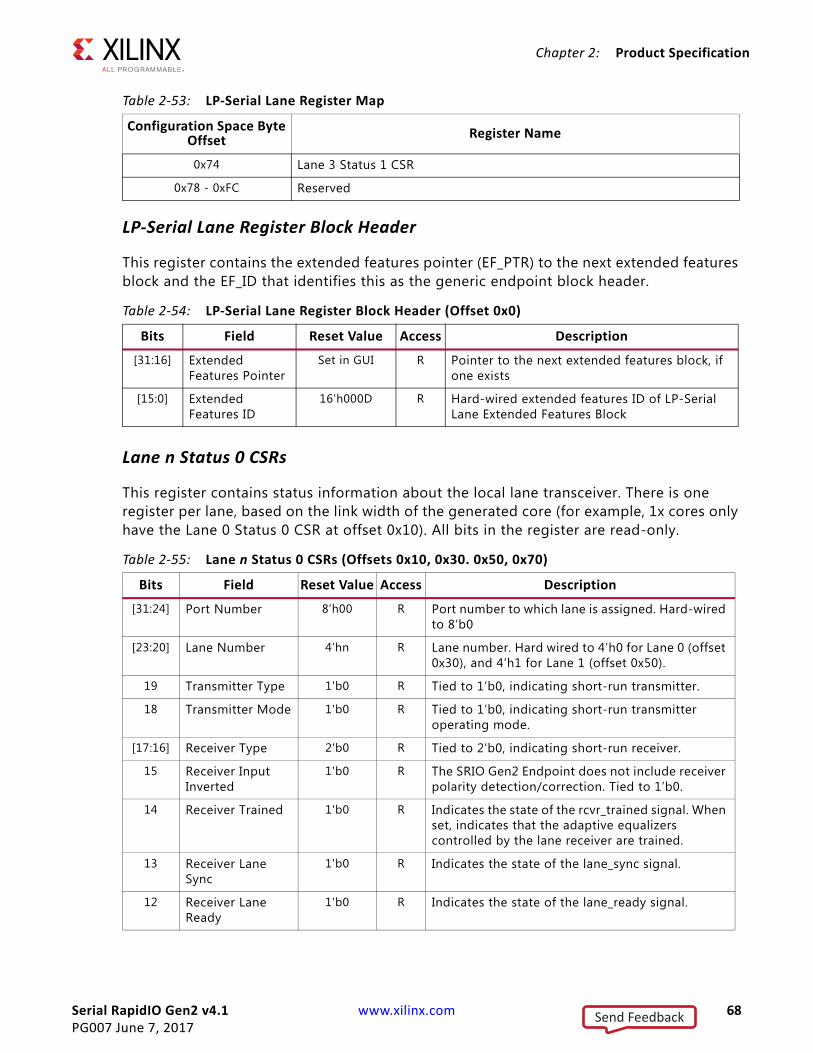
Serial RapidIO Gen2 v4.1 www.xilinx.com 68PG007 June 7, 2017
Chapter 2: Product Specification
LP-Serial Lane Register Block Header
This register contains the extended features pointer (EF_PTR) to the next extended features block and the EF_ID that identifies this as the generic endpoint block header.
Lane n Status 0 CSRs
This register contains status information about the local lane transceiver. There is one register per lane, based on the link width of the generated core (for example, 1x cores only have the Lane 0 Status 0 CSR at offset 0x10). All bits in the register are read-only.
0x74 Lane 3 Status 1 CSR
0x78 - 0xFC Reserved
Table 2-54: LP-Serial Lane Register Block Header (Offset 0x0)
Bits Field Reset Value Access Description
[31:16] Extended Features Pointer
Set in GUI R Pointer to the next extended features block, if one exists
[15:0] Extended Features ID
16’h000D R Hard-wired extended features ID of LP-Serial Lane Extended Features Block
Table 2-55: Lane n Status 0 CSRs (Offsets 0x10, 0x30. 0x50, 0x70)
Bits Field Reset Value Access Description
[31:24] Port Number 8’h00 R Port number to which lane is assigned. Hard-wired to 8’b0
[23:20] Lane Number 4’hn R Lane number. Hard wired to 4’h0 for Lane 0 (offset 0x30), and 4’h1 for Lane 1 (offset 0x50).
19 Transmitter Type 1'b0 R Tied to 1’b0, indicating short-run transmitter.
18 Transmitter Mode 1'b0 R Tied to 1’b0, indicating short-run transmitter operating mode.
[17:16] Receiver Type 2'b0 R Tied to 2’b0, indicating short-run receiver.
15 Receiver Input Inverted
1'b0 R The SRIO Gen2 Endpoint does not include receiver polarity detection/correction. Tied to 1’b0.
14 Receiver Trained 1'b0 R Indicates the state of the rcvr_trained signal. When set, indicates that the adaptive equalizers controlled by the lane receiver are trained.
13 Receiver Lane Sync
1'b0 R Indicates the state of the lane_sync signal.
12 Receiver Lane Ready
1'b0 R Indicates the state of the lane_ready signal.
Table 2-53: LP-Serial Lane Register Map
Configuration Space Byte Offset Register Name
Send Feedback
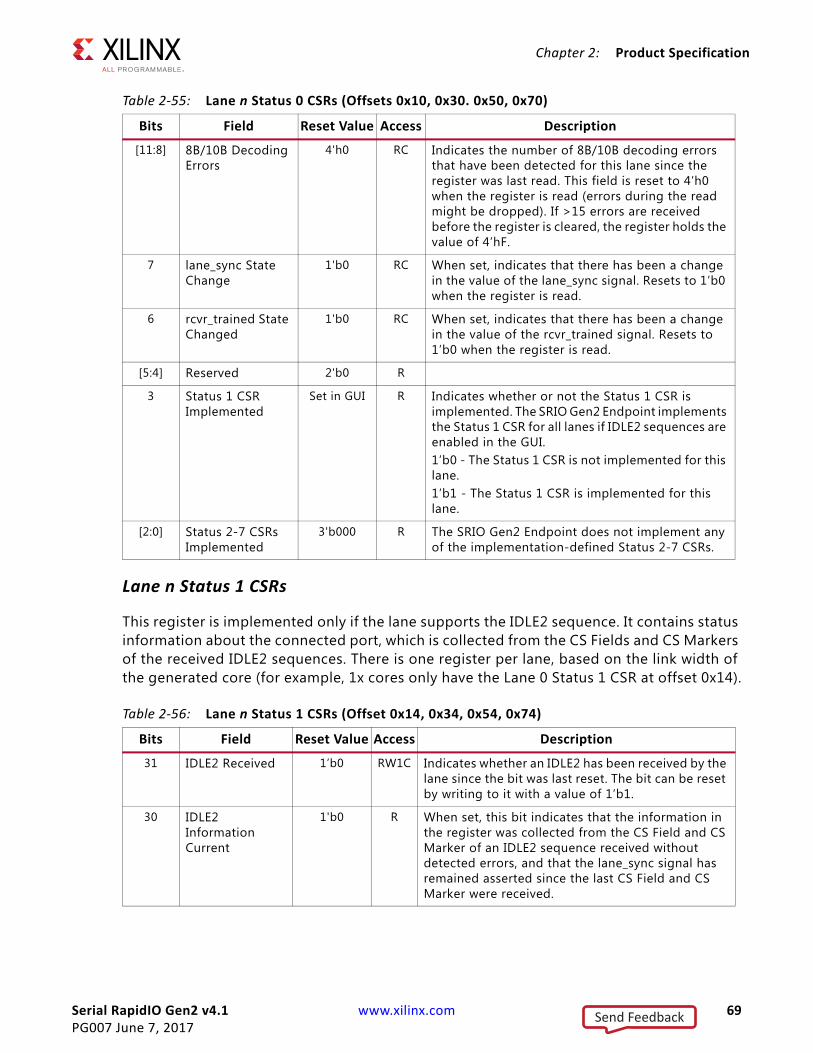
Serial RapidIO Gen2 v4.1 www.xilinx.com 69PG007 June 7, 2017
Chapter 2: Product Specification
Lane n Status 1 CSRs
This register is implemented only if the lane supports the IDLE2 sequence. It contains status information about the connected port, which is collected from the CS Fields and CS Markers of the received IDLE2 sequences. There is one register per lane, based on the link width of the generated core (for example, 1x cores only have the Lane 0 Status 1 CSR at offset 0x14).
[11:8] 8B/10B Decoding Errors
4'h0 RC Indicates the number of 8B/10B decoding errors that have been detected for this lane since the register was last read. This field is reset to 4’h0 when the register is read (errors during the read might be dropped). If >15 errors are received before the register is cleared, the register holds the value of 4’hF.
7 lane_sync State Change
1'b0 RC When set, indicates that there has been a change in the value of the lane_sync signal. Resets to 1’b0 when the register is read.
6 rcvr_trained State Changed
1'b0 RC When set, indicates that there has been a change in the value of the rcvr_trained signal. Resets to 1’b0 when the register is read.
[5:4] Reserved 2'b0 R
3 Status 1 CSR Implemented
Set in GUI R Indicates whether or not the Status 1 CSR is implemented. The SRIO Gen2 Endpoint implements the Status 1 CSR for all lanes if IDLE2 sequences are enabled in the GUI.1’b0 - The Status 1 CSR is not implemented for this lane.1’b1 - The Status 1 CSR is implemented for this lane.
[2:0] Status 2-7 CSRs Implemented
3'b000 R The SRIO Gen2 Endpoint does not implement any of the implementation-defined Status 2-7 CSRs.
Table 2-56: Lane n Status 1 CSRs (Offset 0x14, 0x34, 0x54, 0x74)
Bits Field Reset Value Access Description
31 IDLE2 Received 1’b0 RW1C Indicates whether an IDLE2 has been received by the lane since the bit was last reset. The bit can be reset by writing to it with a value of 1’b1.
30 IDLE2 Information Current
1'b0 R When set, this bit indicates that the information in the register was collected from the CS Field and CS Marker of an IDLE2 sequence received without detected errors, and that the lane_sync signal has remained asserted since the last CS Field and CS Marker were received.
Table 2-55: Lane n Status 0 CSRs (Offsets 0x10, 0x30. 0x50, 0x70)
Bits Field Reset Value Access Description
Send Feedback
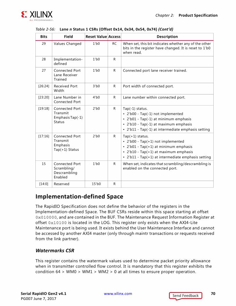
Serial RapidIO Gen2 v4.1 www.xilinx.com 70PG007 June 7, 2017
Chapter 2: Product Specification
Implementation-defined SpaceThe RapidIO Specification does not define the behavior of the registers in the Implementation-defined Space. The BUF CSRs reside within this space starting at offset 0x010000, and are contained in the BUF. The Maintenance Request Information Register at offset 0x10100 is located in the LOG. This register only exists when the AXI4-Lite Maintenance port is being used. It exists behind the User Maintenance Interface and cannot be accessed by another AXI4 master (only through maintr transactions or requests received from the link partner).
Watermarks CSR
This register contains the watermark values used to determine packet priority allowance when in transmitter controlled flow control. It is mandatory that this register exhibits the condition 64 > WM0 > WM1 > WM2 > 0 at all times to ensure proper operation.
29 Values Changed 1'b0 RC When set, this bit indicates whether any of the other bits in the register have changed. It is reset to 1’b0 when read.
28 Implementation-defined
1'b0 R
27 Connected Port Lane Receiver Trained
1'b0 R Connected port lane receiver trained.
[26:24] Received Port Width
3'b0 R Port width of connected port.
[23:20] Lane Number in Connected Port
4'b0 R Lane number within connected port.
[19:18] Connected Port Transmit Emphasis Tap(-1) Status
2'b0 R Tap(-1) status.• 2’b00 - Tap(-1) not implemented• 2’b01 - Tap(-1) at minimum emphasis• 2’b10 - Tap(-1) at maximum emphasis• 2’b11 - Tap(-1) at intermediate emphasis setting
[17:16] Connected Port Transmit Emphasis Tap(+1) Status
2'b0 R Tap(+1) status.• 2’b00 - Tap(+1) not implemented• 2’b01 - Tap(+1) at minimum emphasis• 2’b10 - Tap(+1) at maximum emphasis• 2’b11 - Tap(+1) at intermediate emphasis setting
15 Connected Port Scrambling/Descrambling Enabled
1'b0 R When set, indicates that scrambling/descrambling is enabled on the connected port.
[14:0] Reserved 15'b0 R
Table 2-56: Lane n Status 1 CSRs (Offset 0x14, 0x34, 0x54, 0x74) (Cont’d)
Bits Field Reset Value Access Description
Send Feedback

Serial RapidIO Gen2 v4.1 www.xilinx.com 71PG007 June 7, 2017
Chapter 2: Product Specification
RECOMMENDED: It is recommended that the size of the buffer be taken into account when assigning the watermark values. Too high of a watermark value for a smaller buffer could cause the core to lock up. If there is concern about the size of the buffer, safe watermark values are WM0=3, WM1=2, WM2=1.
RECOMMENDED: It is also recommended that traffic flow is halted prior to writing this register.
Buffer Control CSR
This register contains status information for the buffer and allows control of Buffer features.
Table 2-57: Watermarks CSR (Offset 0x0)
Bits FieldsReset Value Access Description
[31:22] Reserved 10'h000 R
[21:16] WM2 Set in GUI RW Watermark 2 defines the minimum buffer space necessary within the link partner to transmit a priority 2 packet. WM1 > WM2 > 0
[15:14] Reserved 2'b000 R
[13:8] WM1 Set in GUI RW Watermark 1 defines the minimum buffer space necessary within the link partner to transmit a priority 1 packet. WM0 > WM1 > WM2
[7:6] Reserved 2'b000 R
[5:0] WM0 Set in GUI RW Watermark 0 defines the minimum buffer space necessary within the link partner to transmit a priority 0 packet. 64 > WM0 > WM1
Table 2-58: Buffer Control CSR (Offset 0x4)
Bits FieldReset Value Access Description
31 RX Flow Control Only
Set in GUI R BUF was generated with RX flow control only and does not support TX flow control.
30 Unified Clock
Set in GUI R BUF was generated as a unified clock implementation and does not contain clock synchronization logic. Care must be taken to ensure the LOG and PHY clocks are the same. This option should not be used if the core encounters a traindown situation.
29 TX Flow Control
Set in GUI R When asserted to 1'b1, indicates the BUF is currently operating in TX flow control mode.
28 TX Request Reorder
Set in GUI R When asserted to 1'b1, indicates the Transmit Buffer has been configured to allow reordering of requests.
Send Feedback

Serial RapidIO Gen2 v4.1 www.xilinx.com 72PG007 June 7, 2017
Chapter 2: Product Specification
Maintenance Request Information Register
This CSR is used to populate the fields of remote requests sent through the AXI4-Lite Maintenance port. The register is stored within the main LOG rather than with the Serial RapidIO Registers accessible through the Configuration Register Interface. To set the Destination ID, TID, priority, or CRF independently for each outgoing maintenance request, this register must be written before each remote maintenance request.
27 Reserved 1’b0 R
[26:16] TX Size Set in GUI R Number of total unacknowledged packets the TX Buffer can hold. Possible values are 8, 16 or 32.
15 Force RX Flow Control
Default to bit 31
RW Force a TX Flow Control enabled core to use RX flow control. This bit is not writable if the core was generated with the RX Flow Control Only option (in which case, bit 31 is set).
[14:8] Reserved 7'h00 R
[7:0] RX Size Set in GUI R Number of maximum-sized packets the RX Buffer can hold. Possible values are 8, 16 or 32.
Table 2-59: Maintenance Request Information Register (Offset 0x0)
Bits Field Reset Value Access Description
[31:24] Request TID 8'b0 RW The TID used for the next outgoing maintenance request. The value will increment after each request is sent.
[23:19] Reserved 5'b0 R
[18:17] Request Priority 2'b01 RW Priority used for outgoing maintenance requests.
[16] Request CRF 1’b0 RW CRF value used for outgoing maintenance requests.This bit is read-only if the CRF support is disabled in the Vivado IDE.
[15:0] Request Destination ID
16’b0 RW DestID used for outgoing maintenance requests.
Table 2-58: Buffer Control CSR (Offset 0x4)
Bits FieldReset Value Access Description
Send Feedback
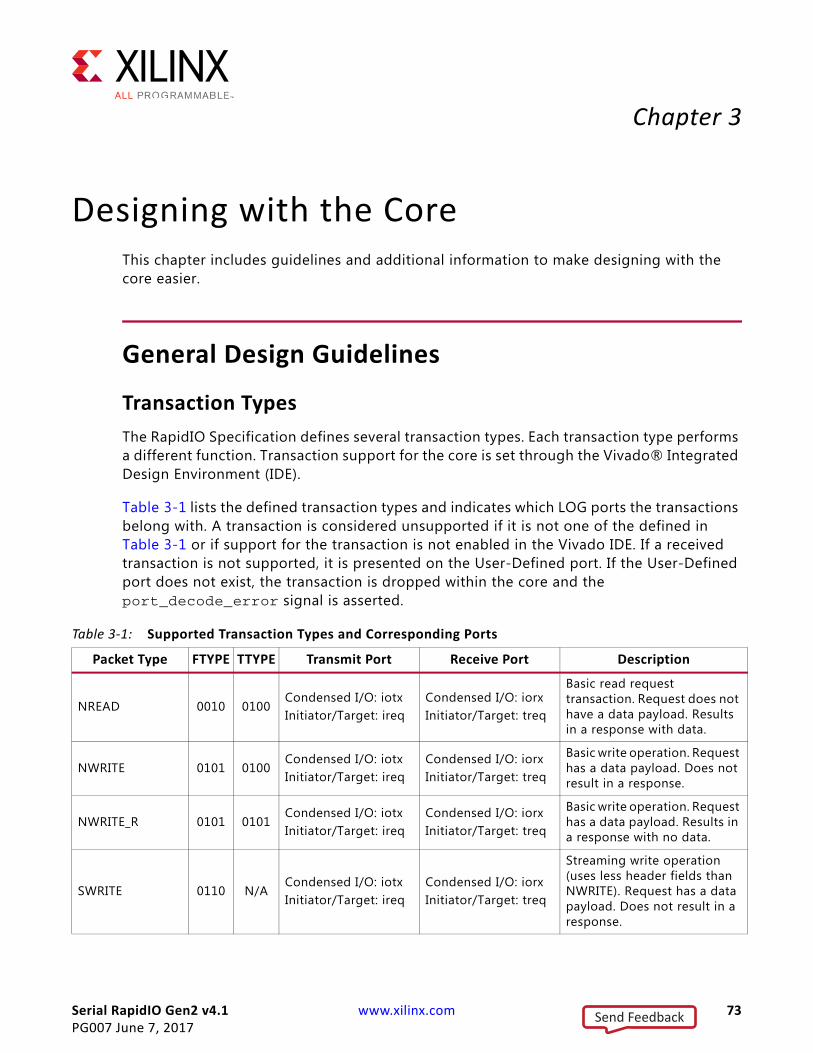
Serial RapidIO Gen2 v4.1 www.xilinx.com 73PG007 June 7, 2017
Chapter 3
Designing with the CoreThis chapter includes guidelines and additional information to make designing with the core easier.
General Design Guidelines
Transaction TypesThe RapidIO Specification defines several transaction types. Each transaction type performs a different function. Transaction support for the core is set through the Vivado® Integrated Design Environment (IDE).
Table 3-1 lists the defined transaction types and indicates which LOG ports the transactions belong with. A transaction is considered unsupported if it is not one of the defined in Table 3-1 or if support for the transaction is not enabled in the Vivado IDE. If a received transaction is not supported, it is presented on the User-Defined port. If the User-Defined port does not exist, the transaction is dropped within the core and the port_decode_error signal is asserted.
Table 3-1: Supported Transaction Types and Corresponding Ports
Packet Type FTYPE TTYPE Transmit Port Receive Port Description
NREAD 0010 0100Condensed I/O: iotxInitiator/Target: ireq
Condensed I/O: iorxInitiator/Target: treq
Basic read request transaction. Request does not have a data payload. Results in a response with data.
NWRITE 0101 0100Condensed I/O: iotxInitiator/Target: ireq
Condensed I/O: iorxInitiator/Target: treq
Basic write operation. Request has a data payload. Does not result in a response.
NWRITE_R 0101 0101Condensed I/O: iotxInitiator/Target: ireq
Condensed I/O: iorxInitiator/Target: treq
Basic write operation. Request has a data payload. Results in a response with no data.
SWRITE 0110 N/ACondensed I/O: iotxInitiator/Target: ireq
Condensed I/O: iorxInitiator/Target: treq
Streaming write operation (uses less header fields than NWRITE). Request has a data payload. Does not result in a response.
Send Feedback
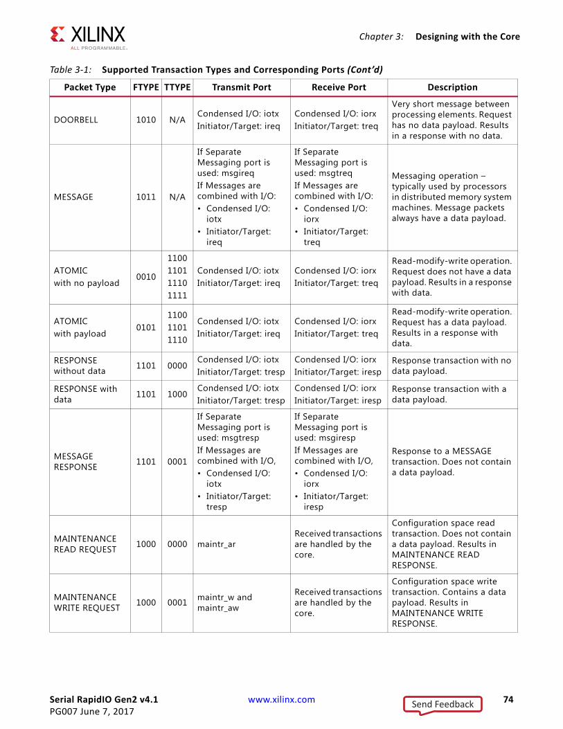
Serial RapidIO Gen2 v4.1 www.xilinx.com 74PG007 June 7, 2017
Chapter 3: Designing with the Core
DOORBELL 1010 N/ACondensed I/O: iotxInitiator/Target: ireq
Condensed I/O: iorxInitiator/Target: treq
Very short message between processing elements. Request has no data payload. Results in a response with no data.
MESSAGE 1011 N/A
If Separate Messaging port is used: msgireqIf Messages are combined with I/O:• Condensed I/O:
iotx• Initiator/Target:
ireq
If Separate Messaging port is used: msgtreqIf Messages are combined with I/O:• Condensed I/O:
iorx• Initiator/Target:
treq
Messaging operation – typically used by processors in distributed memory system machines. Message packets always have a data payload.
ATOMICwith no payload
0010
1100110111101111
Condensed I/O: iotxInitiator/Target: ireq
Condensed I/O: iorxInitiator/Target: treq
Read-modify-write operation. Request does not have a data payload. Results in a response with data.
ATOMICwith payload
0101110011011110
Condensed I/O: iotxInitiator/Target: ireq
Condensed I/O: iorxInitiator/Target: treq
Read-modify-write operation. Request has a data payload. Results in a response with data.
RESPONSE without data 1101 0000
Condensed I/O: iotxInitiator/Target: tresp
Condensed I/O: iorxInitiator/Target: iresp
Response transaction with no data payload.
RESPONSE with data 1101 1000
Condensed I/O: iotxInitiator/Target: tresp
Condensed I/O: iorxInitiator/Target: iresp
Response transaction with a data payload.
MESSAGE RESPONSE 1101 0001
If Separate Messaging port is used: msgtrespIf Messages are combined with I/O,• Condensed I/O:
iotx• Initiator/Target:
tresp
If Separate Messaging port is used: msgirespIf Messages are combined with I/O,• Condensed I/O:
iorx• Initiator/Target:
iresp
Response to a MESSAGE transaction. Does not contain a data payload.
MAINTENANCE READ REQUEST 1000 0000 maintr_ar
Received transactions are handled by the core.
Configuration space read transaction. Does not contain a data payload. Results in MAINTENANCE READ RESPONSE.
MAINTENANCE WRITE REQUEST 1000 0001 maintr_w and
maintr_aw
Received transactions are handled by the core.
Configuration space write transaction. Contains a data payload. Results in MAINTENANCE WRITE RESPONSE.
Table 3-1: Supported Transaction Types and Corresponding Ports (Cont’d)
Packet Type FTYPE TTYPE Transmit Port Receive Port Description
Send Feedback
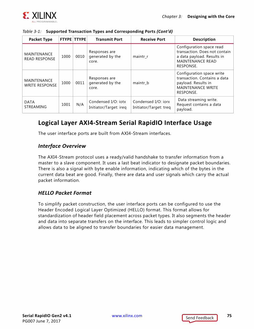
Serial RapidIO Gen2 v4.1 www.xilinx.com 75PG007 June 7, 2017
Chapter 3: Designing with the Core
Logical Layer AXI4-Stream Serial RapidIO Interface UsageThe user interface ports are built from AXI4-Stream interfaces.
Interface Overview
The AXI4-Stream protocol uses a ready/valid handshake to transfer information from a master to a slave component. It uses a last beat indicator to designate packet boundaries. There is also a signal with byte enable information, indicating which of the bytes in the current data beat are good. Finally, there are data and user signals which carry the actual packet information.
HELLO Packet Format
To simplify packet construction, the user interface ports can be configured to use the Header Encoded Logical Layer Optimized (HELLO) format. This format allows for standardization of header field placement across packet types. It also segments the header and data into separate transfers on the interface. This leads to simpler control logic and allows data to be aligned to transfer boundaries for easier data management.
MAINTENANCE READ RESPONSE 1000 0010
Responses are generated by the core.
maintr_r
Configuration space read transaction. Does not contain a data payload. Results in MAINTENANCE READ RESPONSE.
MAINTENANCE WRITE RESPONSE 1000 0011
Responses are generated by the core.
maintr_b
Configuration space write transaction. Contains a data payload. Results in MAINTENANCE WRITE RESPONSE.
DATA STREAMING 1001 N/A
Condensed I/O: iotxInitiator/Target: ireq
Condensed I/O: iorxInitiator/Target: treq
Data streaming write. Request contains a data payload.
Table 3-1: Supported Transaction Types and Corresponding Ports (Cont’d)
Packet Type FTYPE TTYPE Transmit Port Receive Port Description
Send Feedback
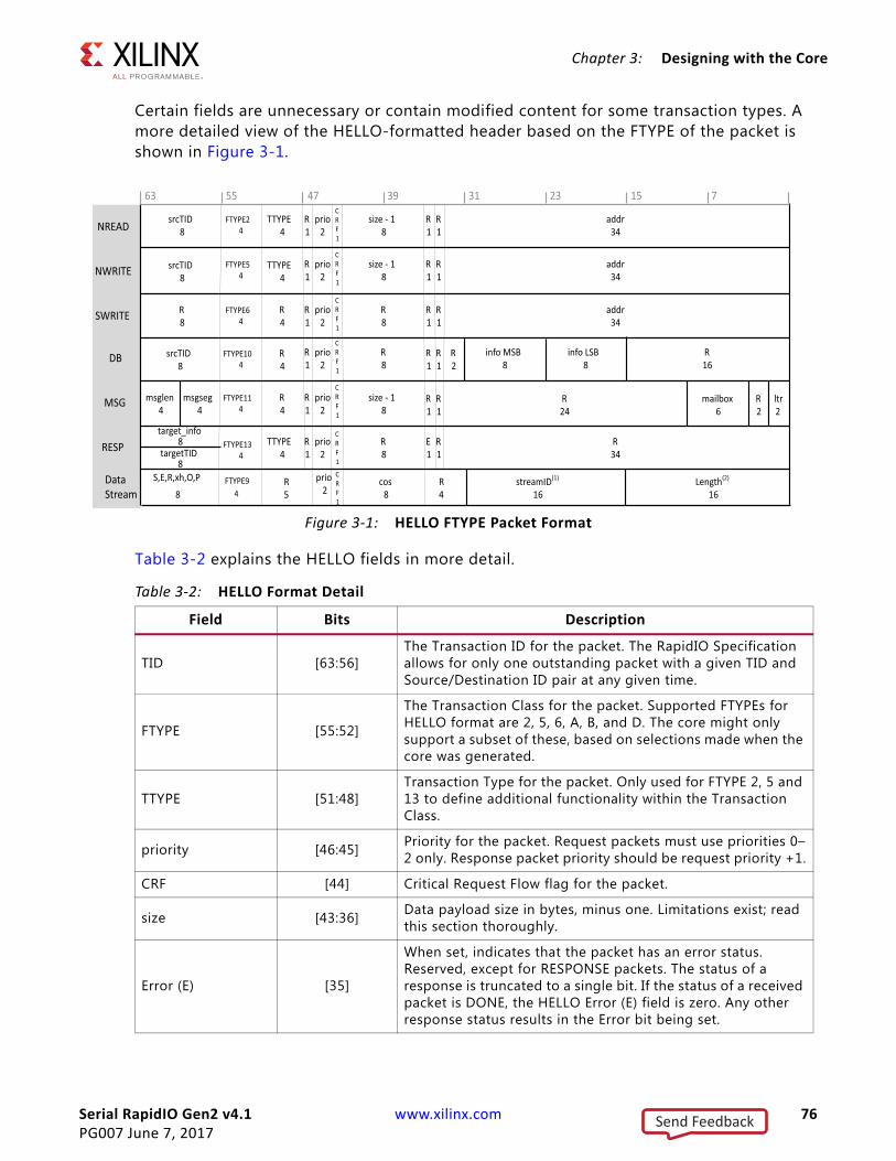
Serial RapidIO Gen2 v4.1 www.xilinx.com 76PG007 June 7, 2017
Chapter 3: Designing with the Core
Certain fields are unnecessary or contain modified content for some transaction types. A more detailed view of the HELLO-formatted header based on the FTYPE of the packet is shown in Figure 3-1.
Table 3-2 explains the HELLO fields in more detail.
X-Ref Target - Figure 3-1
Figure 3-1: HELLO FTYPE Packet Format
NREAD
NWRITE
SWRITE
DB
MSG
RESP
63 55 47 39 31 23 15 7
srcTID8
srcTID8
R8
srcTID8
msglen4
target_info8
targetTID8
msgseg4
FTYPE24
TTYPE4
TTYPE4
TTYPE4
R4
R4
R4
FTYPE54
FTYPE64
FTYPE104
FTYPE114
FTYPE134
R1
addr34
addr34
addr34
R1
R1
R1
R1
R1
E1
R1
R1
R1
R1
R2
R1
R1
R24
mailbox6
R2
ltr2
R34
R1
R1
R1
R1
R1
prio2
prio2
prio2
prio2
prio2
size - 18
size - 18
size - 18
R8
R8
CRF1
CRF1
CRF1
CRF1
CRF1
info MSB8
info LSB8
R16
Data Stream
S,E,R,xh,O,P
8FTYPE9
4
prio2
prio2
CRF1
CRF1
R8
R5
R4
cos8 16
Length(2)
16streamID(1)
Table 3-2: HELLO Format Detail
Field Bits Description
TID [63:56]The Transaction ID for the packet. The RapidIO Specification allows for only one outstanding packet with a given TID and Source/Destination ID pair at any given time.
FTYPE [55:52]
The Transaction Class for the packet. Supported FTYPEs for HELLO format are 2, 5, 6, A, B, and D. The core might only support a subset of these, based on selections made when the core was generated.
TTYPE [51:48]Transaction Type for the packet. Only used for FTYPE 2, 5 and 13 to define additional functionality within the Transaction Class.
priority [46:45] Priority for the packet. Request packets must use priorities 0–2 only. Response packet priority should be request priority +1.
CRF [44] Critical Request Flow flag for the packet.
size [43:36] Data payload size in bytes, minus one. Limitations exist; read this section thoroughly.
Error (E) [35]
When set, indicates that the packet has an error status. Reserved, except for RESPONSE packets. The status of a response is truncated to a single bit. If the status of a received packet is DONE, the HELLO Error (E) field is zero. Any other response status results in the Error bit being set.
Send Feedback
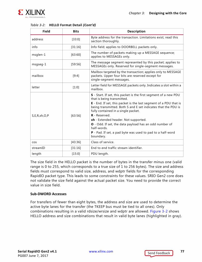
Serial RapidIO Gen2 v4.1 www.xilinx.com 77PG007 June 7, 2017
Chapter 3: Designing with the Core
The size field in the HELLO packet is the number of bytes in the transfer minus one (valid range is 0 to 255, which corresponds to a true size of 1 to 256 bytes). The size and address fields must correspond to valid size, address, and wdptr fields for the corresponding RapidIO packet type. This leads to some constraints for these values. SRIO Gen2 core does not validate the size field against the actual packet size. You need to provide the correct value in size field.
Sub-DWORD Accesses
For transfers of fewer than eight bytes, the address and size are used to determine the active byte lanes for the transfer (the TKEEP bus must be tied to all ones). Only combinations resulting in a valid rdsize/wrsize and wdptr are allowed. Figure 3-2 shows HELLO address and size combinations that result in valid byte lanes (highlighted in gray).
address [33:0] Byte address for the transaction. Limitations exist; read this section thoroughly.
info [31:16] Info field; applies to DOORBELL packets only.
msglen-1 [63:60] The number of packets making up a MESSAGE sequence; applies to MESSAGEs only.
msgseg-1 [59:56] The message segment represented by this packet; applies to MESSAGEs only. Reserved for single-segment messages.
mailbox [9:4]Mailbox targeted by the transaction; applies only to MESSAGE packets. Upper four bits are reserved except for single-segment messages.
letter [1:0] Letter field for MESSAGE packets only. Indicates a slot within a mailbox.
S,E,R,xh,O,P [63:56]
S - Start. If set, this packet is the first segment of a new PDU that is being transmitted. E - End. If set, this packet is the last segment of a PDU that is being transmitted. Both S and E set indicates that the PDU is fully contained in a single packet. R - Reserved. xh - Extended header. Not supported. O - Odd. If set, the data payload has an odd number of half-words. P - Pad. If set, a pad byte was used to pad to a half-word boundary.
cos [43:36] Class of service.
streamID [31:16] End to end traffic stream identifier.
length [15:0] PDU length.
Table 3-2: HELLO Format Detail (Cont’d)
Field Bits Description
Send Feedback
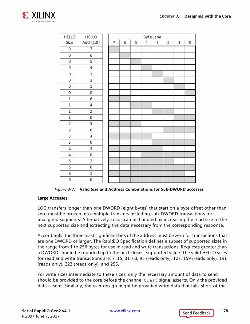
Serial RapidIO Gen2 v4.1 www.xilinx.com 78PG007 June 7, 2017
Chapter 3: Designing with the Core
Large Accesses
LOG transfers longer than one DWORD (eight bytes) that start on a byte offset other than zero must be broken into multiple transfers including sub-DWORD transactions for unaligned segments. Alternatively, reads can be handled by increasing the read size to the next supported size and extracting the data necessary from the corresponding response.
Accordingly, the three least significant bits of the address must be zero for transactions that are one DWORD or larger. The RapidIO Specification defines a subset of supported sizes in the range from 1 to 256 bytes for use in read and write transactions. Requests greater than a DWORD should be rounded up to the next closest supported value. The valid HELLO sizes for read and write transactions are: 7, 15, 31, 63, 95 (reads only), 127, 159 (reads only), 191 (reads only), 223 (reads only), and 255.
For write sizes intermediate to these sizes, only the necessary amount of data to send should be provided to the core before the channel tlast signal asserts. Only the provided data is sent. Similarly, the user design might be provided write data that falls short of the
X-Ref Target - Figure 3-2
Figure 3-2: Valid Size and Address Combinations for Sub-DWORD accesses
Send Feedback

Serial RapidIO Gen2 v4.1 www.xilinx.com 79PG007 June 7, 2017
Chapter 3: Designing with the Core
advertised size. The available data should be written and the transfer should be presumed complete.
The RapidIO Specification does not support data transfer sizes of greater than 256 bytes, and the LOG does not break large transactions into smaller segments. Failure to comply with this requirement can lead to a fatal link error in which the link partner continually retries the oversized packet.
The HELLO header is presented on the first transfer on the user interface ports. If there is data associated with the transaction, it is presented on subsequent beats. The Source and Destination IDs for the packet are placed on the user signal and sampled on the first transfer for each packet. The user signal is ignored after the first beat.
Figure 3-3 shows a typical transfer with data on one of the user interface ports. This particular transfer has a data payload of four DWORDs (32 bytes). On the interface, it takes five total cycles including the transfer of the header.
Figure 3-4 shows a more complicated traffic flow. First, there are two back-to-back single cycle (header-only) packets. The packet boundaries are indicated by the assertion of the TLAST signal. After the single-cycle packets, the master waits one cycle before starting the next packet. In the third packet, both the master and slave each stall the interface on a different cycle (by deasserting TVALID and TREADY respectively). This packet had two
X-Ref Target - Figure 3-3
Figure 3-3: Basic HELLO Packet Transfer on User Interface
log_clk
tvalid
tready
tlast
tdata
tkeep
tuser
HDR D0 D1 D2 D3
8’hFF
ID
Send Feedback
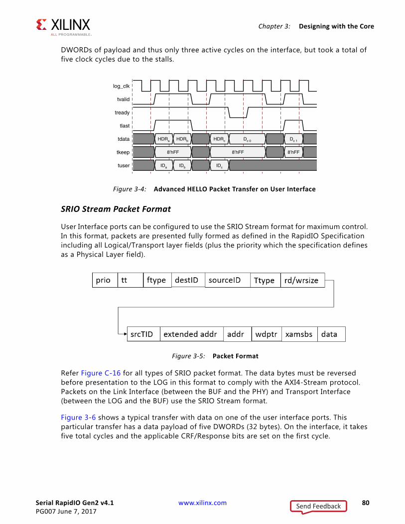
Serial RapidIO Gen2 v4.1 www.xilinx.com 80PG007 June 7, 2017
Chapter 3: Designing with the Core
DWORDs of payload and thus only three active cycles on the interface, but took a total of five clock cycles due to the stalls.
SRIO Stream Packet Format
User Interface ports can be configured to use the SRIO Stream format for maximum control. In this format, packets are presented fully formed as defined in the RapidIO Specification including all Logical/Transport layer fields (plus the priority which the specification defines as a Physical Layer field).
Refer Figure C-16 for all types of SRIO packet format. The data bytes must be reversed before presentation to the LOG in this format to comply with the AXI4-Stream protocol. Packets on the Link Interface (between the BUF and the PHY) and Transport Interface (between the LOG and the BUF) use the SRIO Stream format.
Figure 3-6 shows a typical transfer with data on one of the user interface ports. This particular transfer has a data payload of five DWORDs (32 bytes). On the interface, it takes five total cycles and the applicable CRF/Response bits are set on the first cycle.
X-Ref Target - Figure 3-4
Figure 3-4: Advanced HELLO Packet Transfer on User Interface
X-Ref Target - Figure 3-5
Figure 3-5: Packet Format
log_clk
tvalid
tready
tlast
tdata
tkeep
tuser
HDRa HDRb HDRc Dc 0 Dc 1
8’hFF 8’hFF 8’hFF
IDa IDb IDc
Send Feedback
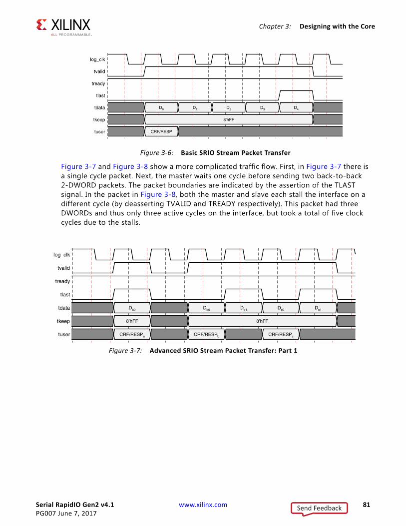
Serial RapidIO Gen2 v4.1 www.xilinx.com 81PG007 June 7, 2017
Chapter 3: Designing with the Core
Figure 3-7 and Figure 3-8 show a more complicated traffic flow. First, in Figure 3-7 there is a single cycle packet. Next, the master waits one cycle before sending two back-to-back 2-DWORD packets. The packet boundaries are indicated by the assertion of the TLAST signal. In the packet in Figure 3-8, both the master and slave each stall the interface on a different cycle (by deasserting TVALID and TREADY respectively). This packet had three DWORDs and thus only three active cycles on the interface, but took a total of five clock cycles due to the stalls.
X-Ref Target - Figure 3-6
Figure 3-6: Basic SRIO Stream Packet Transfer
log_clk
tvalid
tready
tlast
tdata
tkeep
tuser
D0 D1 D2 D3 D4
8’hFF
CRF/RESP
X-Ref Target - Figure 3-7
Figure 3-7: Advanced SRIO Stream Packet Transfer: Part 1
Send Feedback

Serial RapidIO Gen2 v4.1 www.xilinx.com 82PG007 June 7, 2017
Chapter 3: Designing with the Core
Accessing the Configuration SpaceEach processing element connected through the RapidIO fabric has capability registers (CARs) and command and status registers (CSRs). These can be accessed to determine or set the capabilities, configuration, and status of the device. The configuration registers are defined in the RapidIO Specification for each layer. See Chapter 2, Product Specification for detailed information about these registers in the Xilinx Configuration Space.
The registers are 32-bits. All configuration register read and write accesses are performed in word (4-byte) increments. The SRIO Gen2 Endpoint does not support other sizes for Maintenance transactions, including LCSBA transactions. Read and write accesses to reserved register offsets terminate normally and do not result in an error condition. Similarly, writes to CARs (read-only registers) terminate normally and do not result in an error condition.
Using the AXI4-Lite Maintenance Port
Maintenance Write Example
For write transactions, both the write address and write data must be transferred on their respective channels on the Maintenance port before the write is forwarded. When a response is received by the LOG, the Maintenance port returns a status on the write response channel. The Maintenance port only accepts one write at a time (new address and data are not accepted until the response is transferred).
X-Ref Target - Figure 3-8
Figure 3-8: Advanced SRIO Stream Packet Transfer: Part 2
Send Feedback

Serial RapidIO Gen2 v4.1 www.xilinx.com 83PG007 June 7, 2017
Chapter 3: Designing with the Core
Figure 3-9 is a timing diagram showing an example of two write transactions on the Maintenance port. Because the address and data are on separate channels, they can be transferred on the port at any time with respect to one another.
Maintenance Read Example
A read transaction is forwarded immediately after the read address is transferred on the Maintenance port. When the response is received by the LOG, the Maintenance port returns a status on the read response channel. The Maintenance port only accepts one read at a time (a new address is not accepted until the response is transferred).
Figure 3-10 is a timing diagram showing an example of a read transaction on the Maintenance port.
X-Ref Target - Figure 3-9
Figure 3-9: User Maintenance Write Transaction Example
X-Ref Target - Figure 3-10
Figure 3-10: User Maintenance Read Transaction Example
log_clk
maintr_awvalid
maintr_awready
maintr_awaddr
maintr_wvalid
maintr_wready
maintr_wdata
maintr_wstrb
maintr_bvalid
maintr_bready
maintr_bresp
A1 A2
D1 D2
S1 S2
R1 R2
log_clk
maintr_arvalid
maintr_arready
maintr_araddr
maintr_rvalid
maintr_rready
maintr_rresp
maintr_rdata
A1
R1
D1
Send Feedback
Serial RapidIO Gen2 v4.1 www.xilinx.com 84PG007 June 7, 2017
Chapter 3: Designing with the Core
Remotely Accessing the Xilinx Configuration Space
Description
The primary method for accessing the CARs and CSRs that control the LOG, BUF, and PHY functionality from a remote device is through maintenance packets. This includes both maintenance read and write transactions. The configuration space can also be accessed through regular read and write operations, rather than maintenance transactions. This occurs when a NREAD or NWRITE hits the address defined within the Local Configuration Space Base Address (LCSBA) CSR. Specifically, when the two xamsbs bits and the eight most significant bits of the address equal the value in the LCSBA CSR, the read or write request is then treated like a maintenance transaction.
To write to the configuration space of the endpoint, the remote endpoint generates a MAINTENANCE WRITE REQUEST. If the AXI4-Lite Maintenance ports are in use, the write is presented on the cfgr interface. Then, the Configuration Fabric that is part of the reference design routes the write to the appropriate configuration space based on the address of the write. The AXI4-Lite slaves that interface to the configuration registers processes the write and return a response. After completing the write, the LOG issues a MAINTENANCE WRITE RESPONSE back to the remote endpoint indicating the status of the write.
To read from the configuration space of the endpoint, the remote endpoint generates a MAINTENANCE READ REQUEST. If the AXI4-Lite Maintenance ports are in use, the read is presented on the CFGR AXI4-Lite interface. Then, the Configuration Fabric that is part of the reference design routes the read to the appropriate configuration space based on the address of the read (see Table 2-25).
The AXI4-Lite configuration slave processes the read and return a response with data and status information. After issuing the reads, the LOG issues a single MAINTENANCE READ RESPONSE back to the remote endpoint indicating the status of the read and containing the requested data.
Interface
There are no signals required to consume an incoming MAINTENANCE WRITE or READ REQUEST, nor to generate the corresponding MAINTENANCE WRITE or READ RESPONSE when using the AXI4-Lite Maintenance interfaces and the Configuration Fabric reference design delivered with the SRIO Gen2 Endpoint. If the provided reference design is not used, you are responsible for decoding Maintenance transactions and routing them to the AXI4-Lite Configuration Register Interfaces contained within each sub-core.
Remote Maintenance Access Detail
This example details the path followed by a remote MAINTENANCE WRITE transaction when the AXI4-Lite Maintenance Interfaces are in use. The remote endpoint issues a MAINTENANCE REQUEST (ftype=MAINTENANCE and ttype=WRITE REQUEST or READ REQUEST) transaction generated from the remote endpoint. The status is returned through a MAINTENANCE RESPONSE (ftype=MAINTENANCE and ttype=WRITE RESPONSE or READ
Send Feedback
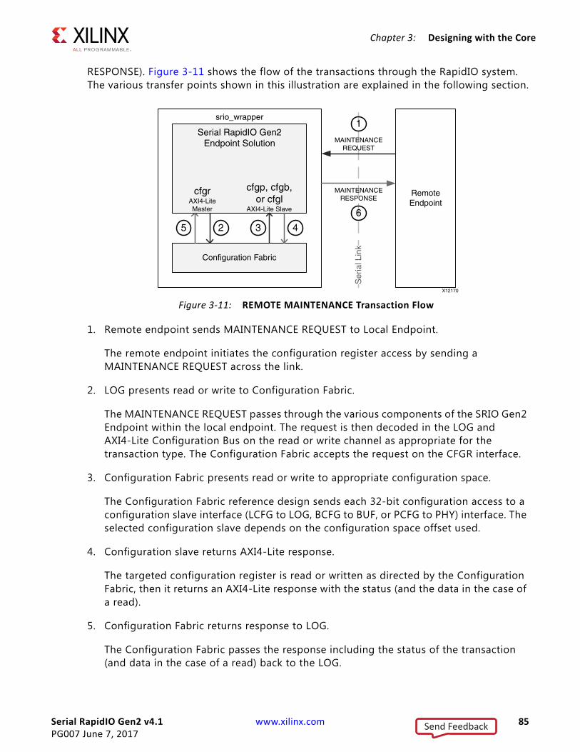
Serial RapidIO Gen2 v4.1 www.xilinx.com 85PG007 June 7, 2017
Chapter 3: Designing with the Core
RESPONSE). Figure 3-11 shows the flow of the transactions through the RapidIO system. The various transfer points shown in this illustration are explained in the following section.
1. Remote endpoint sends MAINTENANCE REQUEST to Local Endpoint.
The remote endpoint initiates the configuration register access by sending a MAINTENANCE REQUEST across the link.
2. LOG presents read or write to Configuration Fabric.
The MAINTENANCE REQUEST passes through the various components of the SRIO Gen2 Endpoint within the local endpoint. The request is then decoded in the LOG and AXI4-Lite Configuration Bus on the read or write channel as appropriate for the transaction type. The Configuration Fabric accepts the request on the CFGR interface.
3. Configuration Fabric presents read or write to appropriate configuration space.
The Configuration Fabric reference design sends each 32-bit configuration access to a configuration slave interface (LCFG to LOG, BCFG to BUF, or PCFG to PHY) interface. The selected configuration slave depends on the configuration space offset used.
4. Configuration slave returns AXI4-Lite response.
The targeted configuration register is read or written as directed by the Configuration Fabric, then it returns an AXI4-Lite response with the status (and the data in the case of a read).
5. Configuration Fabric returns response to LOG.
The Configuration Fabric passes the response including the status of the transaction (and data in the case of a read) back to the LOG.
X-Ref Target - Figure 3-11
Figure 3-11: REMOTE MAINTENANCE Transaction Flow
Send Feedback
Serial RapidIO Gen2 v4.1 www.xilinx.com 86PG007 June 7, 2017
Chapter 3: Designing with the Core
6. Local Endpoint returns MAINTENANCE RESPONSE to the Remote Endpoint.
The LOG forms the MAINTENANCE RESPONSE, using information from the request packet and from the response returned by the Configuration Fabric. The MAINTENANCE RESPONSE packet is passed through the SRIO Gen2 Endpoint across the link to the requesting remote endpoint to complete the maintenance request-response transaction. This response includes a status indicating whether the request was processed successfully and data for unerrored reads.
Special Considerations for Accessing the Xilinx Configuration Space Remotely
If the SRIO Gen2 Endpoint receives a transaction of an unsupported type (LCSBA hit for any packet types except NREAD, NWRITE, and NWRITE_R), it returns an error response. In the case of an errored write, the core does not update the configuration register with the write data from the request. An error response is also returned for MAINTENANCE REQUESTs or LCSBA hits with a request size of anything but one word (four bytes).
Using SRIO Gen2 Endpoint to Access Local Configuration Space
Description
The method for accessing the CARs and CSRs that control the LOG, BUF, and PHY functionality from within the local device is through local maintenance packets. This includes both maintenance read and write transactions. The AXI4-Lite Maintenance port only allows one outstanding read and one outstanding write at any given time. Particularly remote requests can take a significant amount of time to complete. Traffic flow must be planned accordingly.
Interface
The user interface generates the local configuration request on the Maintenance port. See Maintenance Port in Chapter 2 for more details.
Send Feedback

Serial RapidIO Gen2 v4.1 www.xilinx.com 87PG007 June 7, 2017
Chapter 3: Designing with the Core
Local Configuration Access Example
This example details the process for reading or writing to a local configuration register using the AXI4-Lite Maintenance Interface. Figure 3-12 shows the flow of the transactions through the local endpoint.
1. The user interface generates the request.
To initiate the access to the local configuration space, create an AXI4-Lite read or write on the Maintenance port (see Using the AXI4-Lite Maintenance Port).
When setting up the address for the write, the offset of the register is the address of that register. For example, the Base Device ID CSR resides at offset 0x60. This address is passed along through Read Address or Write Address Channel on the Maintenance port. However, configuration offsets are only 24 bits while the maintr_awaddr and maintr_araddr inputs are 32 bits. The upper eight bits are used to set the hop count for the transaction. So for a local write, address bits [31:24] should be zero. For maintenance packets, configuration offsets are placed on maintr_awaddr[23:0] or maintr_araddr[23:0] for writes and reads, respectively.
Note: Because registers are only addressed on a word (four-byte) basis, the lower two bits of address are ignored.
The user interface presents the address on the appropriate address input, then asserts VALID for the channel. For write accesses, the user interface presents 32 bits of data on the write data channel while asserting the maintr_wvalid signal. After the address (and data in the case of a write) is accepted into the core, the LOG processes the transaction.
X-Ref Target - Figure 3-12
Figure 3-12: Local MAINTENANCE Transaction Flow
<component_name>_block
Serial RapidIO Gen2Endpoint Solution
Configuration Fabric
2 3 45
UserApplication
1
6
X12171
maintrAXI4-Lite
Slave
cfgrAXI4-LiteMaster
cfgp, cfgb,or cfgl
AXI4-Lite Slave
Send Feedback
Serial RapidIO Gen2 v4.1 www.xilinx.com 88PG007 June 7, 2017
Chapter 3: Designing with the Core
2. LOG presents transaction to Configuration Fabric.
When the Configuration Fabric Interface is available, the transaction is presented to the Configuration Fabric through the cfgr AXI4-Lite Master.
3. Configuration Fabric forwards transaction to Configuration Registers.
The Configuration Fabric decodes the address of the transaction and presents it to the appropriate Configuration Register Interface.
4. Configuration Register response returned to Configuration Fabric.
After the register is read or updated, a response is presented back from the Configuration Register Interface to the Configuration Fabric.
5. Configuration Fabric returns response to LOG.
The Configuration Fabric forwards the response back to the LOG on the cfgr interface.
6. Response provided to user.
The LOG returns a response including status information (and data for reads) on the appropriate Response Channel of the Maintenance port. See Using the AXI4-Lite Maintenance Port for more information.
Using SRIO Gen2 Endpoint to Access Remote Configuration Space
Description
The primary method for reading or writing configuration registers of a remote device connected through the RapidIO fabric is through maintenance transactions. This includes both maintenance read and write transactions. The configuration space can also be accessed through regular read and write operations, rather than maintenance transactions. This occurs when a NREAD, NWRITE, or SWRITE hits the address defined within the Local Configuration Space Base Address (LCSBA) CSR. Specifically, when the two xamsbs bits and the eight most significant bits of the address equal the value in the LCSBA CAR, the read or write request is then treated like a maintenance transaction. LCSBA transactions targeting remote configuration space must be performed using the I/O ports.
The process for accessing remote configuration space with MAINTENANCE transactions using the AXI4-Lite Maintenance port is very similar to the process used to access the local configuration space with the SRIO Gen2 Endpoint.
Interface
The user interface generates the local configuration request on the Maintenance port (see Maintenance Port in Chapter 2 description for more details).
Send Feedback
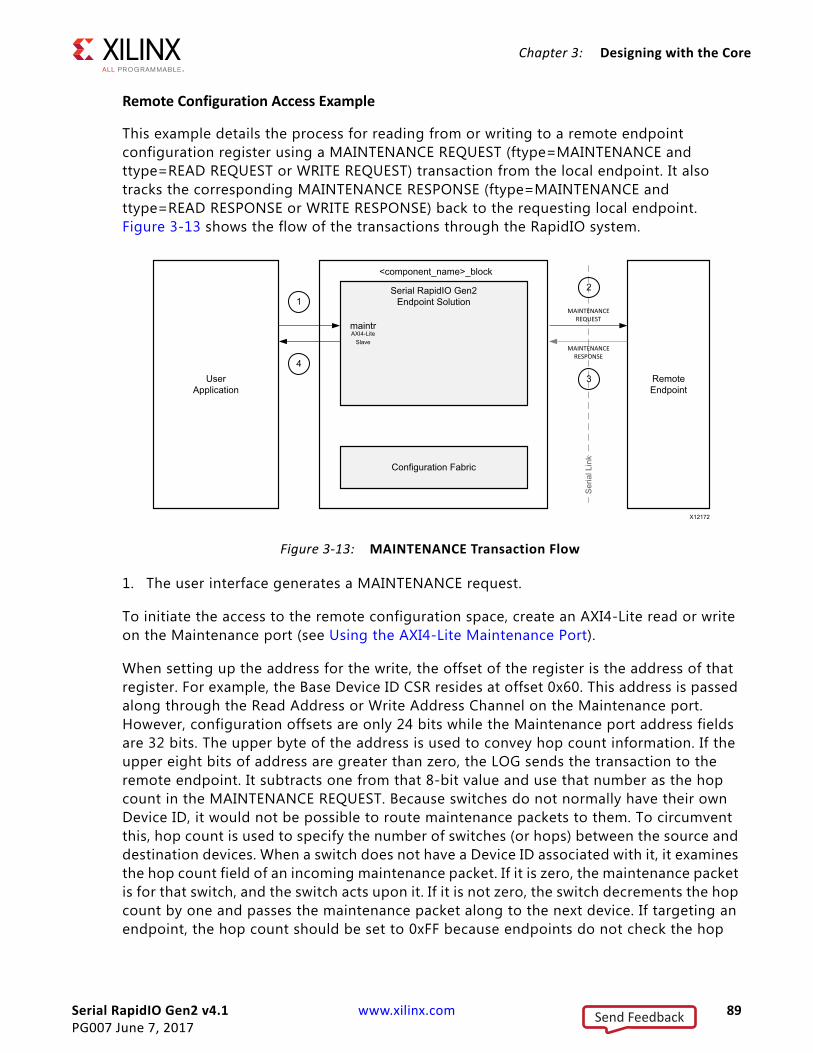
Serial RapidIO Gen2 v4.1 www.xilinx.com 89PG007 June 7, 2017
Chapter 3: Designing with the Core
Remote Configuration Access Example
This example details the process for reading from or writing to a remote endpoint configuration register using a MAINTENANCE REQUEST (ftype=MAINTENANCE and ttype=READ REQUEST or WRITE REQUEST) transaction from the local endpoint. It also tracks the corresponding MAINTENANCE RESPONSE (ftype=MAINTENANCE and ttype=READ RESPONSE or WRITE RESPONSE) back to the requesting local endpoint. Figure 3-13 shows the flow of the transactions through the RapidIO system.
1. The user interface generates a MAINTENANCE request.
To initiate the access to the remote configuration space, create an AXI4-Lite read or write on the Maintenance port (see Using the AXI4-Lite Maintenance Port).
When setting up the address for the write, the offset of the register is the address of that register. For example, the Base Device ID CSR resides at offset 0x60. This address is passed along through the Read Address or Write Address Channel on the Maintenance port. However, configuration offsets are only 24 bits while the Maintenance port address fields are 32 bits. The upper byte of the address is used to convey hop count information. If the upper eight bits of address are greater than zero, the LOG sends the transaction to the remote endpoint. It subtracts one from that 8-bit value and use that number as the hop count in the MAINTENANCE REQUEST. Because switches do not normally have their own Device ID, it would not be possible to route maintenance packets to them. To circumvent this, hop count is used to specify the number of switches (or hops) between the source and destination devices. When a switch does not have a Device ID associated with it, it examines the hop count field of an incoming maintenance packet. If it is zero, the maintenance packet is for that switch, and the switch acts upon it. If it is not zero, the switch decrements the hop count by one and passes the maintenance packet along to the next device. If targeting an endpoint, the hop count should be set to 0xFF because endpoints do not check the hop
X-Ref Target - Figure 3-13
Figure 3-13: MAINTENANCE Transaction Flow
MAINTENANCE REQUEST
<component_name>_block
Serial RapidIO Gen2Endpoint Solution
Configuration Fabric
UserApplication
1
4
X12172
maintrAXI4-Lite
Slave
RemoteEndpoint
2
3
MAINTENANCE RESPONSE
Ser
ial L
ink
Send Feedback
Serial RapidIO Gen2 v4.1 www.xilinx.com 90PG007 June 7, 2017
Chapter 3: Designing with the Core
count when determining if a transaction is intended for it. This is also an easy method to ensure an intermediate switch does not accidently grab the transaction for itself.
Note: Because the LOG only supports word (four-byte) Maintenance Requests, the lowest two bits of address are ignored.
The MAINTENANCE REQUEST uses the value stored in the Base Device ID CSR as the Source ID for the transaction. This value is also available on the deviceid output from the LOG. The priority, CRF, and Destination ID fields are populated with information from the Maintenance Request Information Register (see Maintenance Request Information Register in Chapter 2). To override these values, that register must be written before the remote request is presented to the LOG. The TID used for the Request is also stored in the Maintenance Request Information Register. The LOG starts with a TID of 0 and increments it for every remote request that it generates. The TID that is used on the next request can be read in this register, or can be overwritten with a register write. The process for accessing the Maintenance Request Information Register is the same as that described in Using SRIO Gen2 Endpoint to Access Local Configuration Space.
2. MAINTENANCE REQUEST is transmitted to a remote device.
The LOG forms the MAINTENANCE REQUEST packet, which is forwarded across the link into the RapidIO system.
3. The remote device sends MAINTENANCE RESPONSE to SRIO Gen2 Endpoint.
The targeted device creates a MAINTENANCE RESPONSE and send it back to the SRIO Gen2 Endpoint.
4. The response is returned to the user interface.
After the MAINTENANCE RESPONSE is received by the LOG, it checks the TID against that of the request. If there is a match, the status of the response is returned on the appropriate Maintenance Response channel. For a read response, the data from the MAINTENANCE RESPONSE is also returned on the read response channel of the Maintenance port. See the Using the AXI4-Lite Maintenance Port for signaling information.
Special Considerations for Accessing Remote Configuration Space with the AXI4-Lite Maintenance Port
The LOG allows four-byte configuration accesses only. There can be only one outstanding read and one outstanding write access at any given time (local or remote). The LOG drops MAINTENANCE responses with TIDs that do not match that of the outstanding request. This is done silently and is implemented this way for AXI4-Lite compliance.
A reset is provided on the Maintenance port so that a timeout can be implemented to prevent a lost or improperly formed response from locking up the port indefinitely. When maintr_rst is asserted, outstanding maintenance packets is cancelled. A typical application uses the link_timeout output (which reflects the value stored in the Link
Send Feedback
Serial RapidIO Gen2 v4.1 www.xilinx.com 91PG007 June 7, 2017
Chapter 3: Designing with the Core
Timeout CSR) to set the timeout counter which is only active when a request is outstanding and clears to 0 when a response is received.
RECOMMENDED: It is recommended that the Maintenance port be static at the time of the reset (in other words, do not send a read while attempting to cancel a response-less write).
After the requests have been dropped through maintr_rst, the stored TIDs are cleared for both the read and write paths. This means that if a response is received after the reset assertion for a previous request on either channel, it is dropped silently.
Clocking
Core ClocksThe PHY operates on two clock domains: phy_clk, which is the primary core clock, and gt_pcs_clk, which is used for the Serial Transceiver interface. The gt_clk is not used by the PHY, but is used by the Serial Transceiver interface. The gt_pcs_clk is half the rate of gt_clk. As a general rule, phy_clk is equal to (gt_clk * operating link width)/4. So for a core operating at 2x, phy_clk is half the frequency of gt_clk. If the core trains down to 1x mode, phy_clk must switch to a quarter of the gt_clk rate. The Serial Transceivers also require a reference clock (refclk) that uses the dedicated clock pins of the transceiver. The reference clock frequency is selected when the core is generated (the available options depend on architecture and line rate).
The LOG operates on the log_clk domain. For optimum throughput, log_clk should be at least as fast as phy_clk.
The BUF transfers packets between the log_clk and phy_clk domains. If the BUF is generated for unified clocks, log_clk and phy_clk must be synchronous. Otherwise, the clocks must match the rates of the interfacing sub-cores.
The cfg_clk domain on each sub-core Configuration Register interface is independent of that sub-core clock(s). However, to use the LOG Maintenance Controller with the provided
Table 3-3: Reference Clock Available Per Line Rate
Line Rate (Gb/s) refclk125 MHZ
refclk156.25 MHz
1.25 x
2.5 x
3.125 x x
5 x
6.25 x
Send Feedback
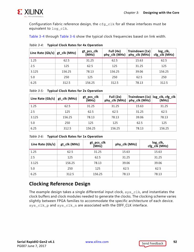
Serial RapidIO Gen2 v4.1 www.xilinx.com 92PG007 June 7, 2017
Chapter 3: Designing with the Core
Configuration Fabric reference design, the cfg_clk for all these interfaces must be equivalent to log_clk.
Table 3-4 through Table 3-6 show the typical clock frequencies based on link width.
Clocking Reference DesignThe example design takes a single differential input clock, sys_clk, and instantiates the clock buffers and clock modules needed to generate the clocks. The clocking scheme varies slightly between FPGA families to accommodate the specific architecture of each device. sys_clk_p and sys_clk_n are associated with the DIFF_CLK interface.
Table 3-4: Typical Clock Rates for 4x Operation
Line Rate (Gb/s) gt_clk (MHz) gt_pcs_clk (MHz)
Full (4x) phy_clk (MHz)
Traindown (1x) phy_clk (MHz)
log_clk,cfg_clk (MHz)
1.25 62.5 31.25 62.5 15.63 62.5
2.5 125 62.5 125 31.25 125
3.125 156.25 78.13 156.25 39.06 156.25
5.0 250 125 250 62.5 250
6.25 312.5 156.25 312.5 78.13 312.5
Table 3-5: Typical Clock Rates for 2x Operation
Line Rate (Gb/s) gt_clk (MHz) gt_pcs_clk (MHz)
Full (2x) phy_clk (MHz)
Traindown (1x) phy_clk (MHz)
log_clk, cfg_clk(MHz)
1.25 62.5 31.25 31.25 15.63 31.25
2.5 125 62.5 62.5 31.25 62.5
3.125 156.25 78.13 78.13 39.06 78.13
5.0 250 125 125 62.5 125
6.25 312.5 156.25 156.25 78.13 156.25
Table 3-6: Typical Clock Rates for 1x Operation
Line Rate (Gb/s) gt_clk (MHz) gt_pcs_clk (MHz) phy_clk (MHz) log_clk,
cfg_clk (MHz)
1.25 62.5 31.25 15.63 15.63
2.5 125 62.5 31.25 31.25
3.125 156.25 78.13 39.06 39.06
5.0 250 125 62.5 62.5
6.25 312.5 156.25 78.13 78.13
Send Feedback

Serial RapidIO Gen2 v4.1 www.xilinx.com 93PG007 June 7, 2017
Chapter 3: Designing with the Core
7 Series Device
For the 7 series FPGAs, an MMCM is used to generate the clocks from the serial transceiver (GT) reference clock. A block diagram of the clocking scheme is shown in Figure 3-14.
The MMCM multiplier and divider values are dependent on the reference clock frequency and the line rate. In 4x configurations, log_clk and gt_clk share a BUFG. In 1x configurations, log_clk and phy_clk share a BUFG (and no BUFGMUX is needed because there is only one possible phy_clk rate). In addition, if the Unified Clock option is selected in the Vivado IDE, log_clk and phy_clk are required to be the same rate. This means the BUFG for the log_clk/cfg_clk can be removed, and the log_clk/cfg_clk is tied to the phy_clk.
UltraScale Device
Figure 3-15 shows the clocking diagram for UltraScale devices. It uses BUFG_GTs instead of MMCM to get the appropriate clock divisions for the core and GT.
X-Ref Target - Figure 3-14
Figure 3-14: Clocking for 7 Series FPGAs
Send Feedback
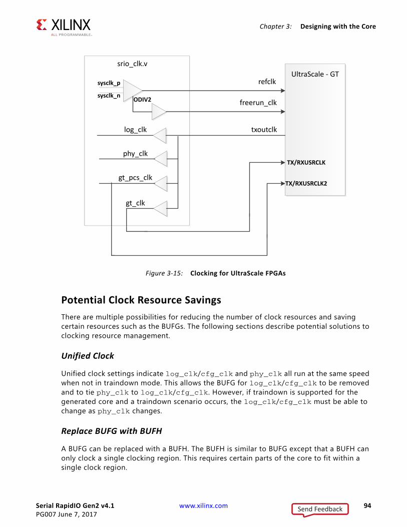
Serial RapidIO Gen2 v4.1 www.xilinx.com 94PG007 June 7, 2017
Chapter 3: Designing with the Core
Potential Clock Resource SavingsThere are multiple possibilities for reducing the number of clock resources and saving certain resources such as the BUFGs. The following sections describe potential solutions to clocking resource management.
Unified Clock
Unified clock settings indicate log_clk/cfg_clk and phy_clk all run at the same speed when not in traindown mode. This allows the BUFG for log_clk/cfg_clk to be removed and to tie phy_clk to log_clk/cfg_clk. However, if traindown is supported for the generated core and a traindown scenario occurs, the log_clk/cfg_clk must be able to change as phy_clk changes.
Replace BUFG with BUFH
A BUFG can be replaced with a BUFH. The BUFH is similar to BUFG except that a BUFH can only clock a single clocking region. This requires certain parts of the core to fit within a single clock region.
X-Ref Target - Figure 3-15
Figure 3-15: Clocking for UltraScale FPGAs
UltraScale - GT
txoutclk
refclk
freerun_clk
TX/RXUSRCLK
sysclk_p
sysclk_nlk ODIV2
log_clk
phy_clk
gt_pcs_clk
gt_clk
TX/RXUSRCLK2
srio_clk.v
Send Feedback
Serial RapidIO Gen2 v4.1 www.xilinx.com 95PG007 June 7, 2017
Chapter 3: Designing with the Core
One specific example is the BUFGs for the gt_clk and the gt_pcs_clk can be replaced with BUFHs. This requires the serial transceivers (GTs) and part of the PHY to fit within a single clock region, which it currently does. The LOC constraint might be required to place the BUFH, GTs, and PHY in the same region.
Another example is the BUFG for the phy_clk can be replaced with a BUFH if there is no requirement for the core to support traindown. This scenario also requires the BUFH and PHY to be in the same clock region.
Note: Every BUFG replaced with a BUFH makes it more difficult to meet timing for the core because of the single clocking region restrictions.
Resource Sharing
Several aspects of resource sharing can occur when multiple instances of the SRIO Gen2 Endpoint are implemented, depending on the configuration and usage of the RapidIO system. If the same line rates, link widths, and user interface clocks are used for each instance (without traindown support), all of the clocking resources can be shared. Up to version 2_0 of the core, the RTL hierarchy for the core was fixed. This resulted in some difficulty because shareable clocking and reset logic needed to be extracted from the core example design for use with a single instance, or multiple instances of the core.
Shared Logic is a new feature that provides a more flexible architecture that works both as a standalone core and as a part of a larger design with one or more core instances. This minimizes the amount of HDL modifications required, but at the same time retains the flexibility to address more uses of the core.
The new level of hierarchy is called <component_name>_support. Figure 3-16 and Figure 3-17 show two hierarchies where the shared logic block is contained either in the core or in the example design. In these figures, <component_name> is the name of the generated core. The difference between the two hierarchies is the boundary of the core. It is controlled using the Shared Logic option in the Vivado IDE (see Figure 4-10).
X-Ref Target - Figure 3-16
Figure 3-16: Shared Logic in the Core
<component_name>_example_design
<component_name>
<component_name>_support
<component_name>_blockSharedLogic
X13768
Send Feedback
Serial RapidIO Gen2 v4.1 www.xilinx.com 96PG007 June 7, 2017
Chapter 3: Designing with the Core
When shared logic (MMCM, Resets and GT COMMON [7 series devices only]) is included in core, all clocks and resets that are used by core are also brought out of <component_name>. When shared logic (MMCM, Resets and GT COMMON) is included in the example design, the <component_name> has all clocks and resets as inputs. This option enables you to share resources across multiple instances. For example, you can generate the first instance of the SRIO Gen2 core with the Include Shared Logic in Core option selected, and subsequent instances with the Include Shared Logic in Example Design option. Then, you can share the resources from the first instance of the core with other instances if they operate with the same rate. Following are some examples of how resources can be shared.
If a design has different line rates, link widths, and might need to support traindown, but has the same user interface clocks for each instance of the RapidIO system, the BUFG for the log_clk/cfg_clk can be shared. Figure 3-18 shows an example of log_clk/cfg_clk resource sharing.
X-Ref Target - Figure 3-17
Figure 3-17: Shared Logic in the Example Design
<component_name>_example_design
<component_name>_support
<component_name>
<component_name>_blockSharedLogic
X13769
Send Feedback
Serial RapidIO Gen2 v4.1 www.xilinx.com 97PG007 June 7, 2017
Chapter 3: Designing with the Core
If a design has the same line rates, but supports different link widths and traindown, and has a different user interface clocks for each instance of the RapidIO system, the BUFGs for
X-Ref Target - Figure 3-18
Figure 3-18: log_clk/cfg_clk Resource Sharing
Send Feedback
Serial RapidIO Gen2 v4.1 www.xilinx.com 98PG007 June 7, 2017
Chapter 3: Designing with the Core
the gt_clk and gt_pcs_clk can be shared. Figure 3-19 shows an example of gt_clk resource sharing.
Figure 3-20 shows all the resources being shared. This scenario assumes all the line rates, link widths, and user interfaces are the same, and that traindown is not supported. In this case, the MMCM and BUFGs are shared between two instances of the RapidIO system. In
X-Ref Target - Figure 3-19
Figure 3-19: gt_clk/gt_pcs_clk Resource Sharing
Send Feedback
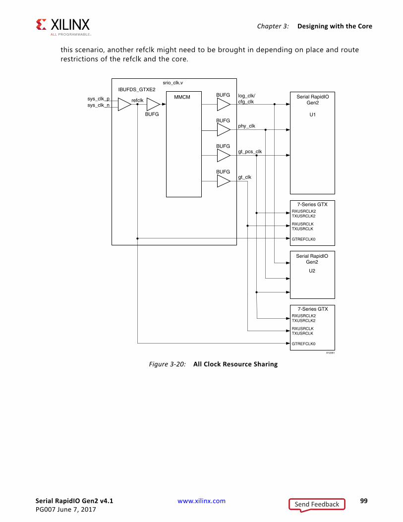
Serial RapidIO Gen2 v4.1 www.xilinx.com 99PG007 June 7, 2017
Chapter 3: Designing with the Core
this scenario, another refclk might need to be brought in depending on place and route restrictions of the refclk and the core. X-Ref Target - Figure 3-20
Figure 3-20: All Clock Resource Sharing
Send Feedback

Serial RapidIO Gen2 v4.1 www.xilinx.com 100PG007 June 7, 2017
Chapter 3: Designing with the Core
ResetsEach clock domain has an associated reset. The reset should be asserted for a minimum of four clock cycles of the respective clock domain and deassert synchronously (note that if the core is trained down, phy_clk runs slower than the original rate and the reset must still assert for four full cycles).
The included reset reference design module (srio_rst.v) has a single reset input, sys_rst. This signal is an asynchronous input. This module synchronizes the reset to each clock domain and extends the pulse to meet the minimum reset cycle requirements.
The initial hardware reset should be generated by the user design. Resets might also be communicated in-band using the RapidIO protocol. Special care must be used when resetting the SRIO Gen2 Endpoint device. Both link partners should be reset together to guarantee ackID alignment. It is recommended that resets between link partners be overlapped to reduce the occurrence of lost packets and control symbols. One way to implement this is to handshake the core resets. Resets received from the link partner are communicated to the user design with the assertion of phy_rcvd_link_reset from the core. The sys_rst signal should be asserted upon receipt of a link reset. Depending on the implementation, a reset can also be signaled to the user application in response to the assertion of phy_rcvd_link_reset. To send a reset request to the link partner, assert the phy_link_reset signal until the port_initialized output goes Low. At this time, sys_rst should be asserted to the reset reference design, completing the handshake.
Shared Logic Related Port DescriptionsTable 3-7 shows the shared logic related port descriptions of <component_name> when Shared Logic is included in core.
Table 3-7: <component_name> Clock And Reset Signals When Shared Logic in Core
Signal Direction Description
sys_clkp Input System differential clock p input.
sys_clkn Input System differential clock n input.
log_clk_out Output This is same as log_clk.
phy_clk_out Output This is same as phy_clk.
gt_clk_out Output This is same as gt_clk.
gt_pcs_clk_out Output This is same as gt_pcs_clk.
drpclk_out Output This is same as phy_clk in 1x mode.
refclk_out Output This is same as refclk.
clk_lock_out Output This is same as clk_lock.
Send Feedback
Serial RapidIO Gen2 v4.1 www.xilinx.com 101PG007 June 7, 2017
Chapter 3: Designing with the Core
Table 3-8 shows the shared logic related port descriptions of <component_name> when Shared Logic is included in example design.
cfg_rst_out Output This is same as cfg_rst.
log_rst_out Output This is same as log_rst.
buf_rst_out Output This is same as buf_rst.
phy_rst_out Output This is same as phy_rst.
gt_pcs_rst_out Output This is same as gt_pcs_rst.
gt0_qpll_lock_out Output This is same as gt0_qpll_lock.
gt0_qpll_clk_out Output This is same as gt0_qpll_clk.
gt0_qpll_out_refclk_out Output This is same as gt0_qpll_out_refclk.
gt0_pll0_clk_out Output This is same as gt0_pll0_clk.
gt0_pll0_ref_clk_out Output This is same as gt0_pll0_refclk.
gt0_pll1_clk_out Output This is same as gt0_pll1_clk.
gt0_pll1_ref_clk_out Output This is same as gt0_pll1_refclk.
gt0_pll0_lock_out Output This is same as gt0_pll0_lock.
Table 3-8: <component_name> Clock And Reset Signals When Shared Logic in Example Design
Signal Direction Description
log_clk_in Input This is same as log_clk.
phy_clk_in Input This is same as phy_clk.
gt_clk_in Input This is same as gt_clk.
gt_pcs_clk_in Input This is same as gt_pcs_clk.
drpclk_in Input As drpclk is connected to plllockdetclk, the requirement on GT plllockdetclk can be found in the GT user guide. The drpclk can be at any clock rate below the maximum frequency stated in the device datasheet.
refclk_in Input This is same as refclk.
clk_lock_in Input This is same as clk_lock.
cfg_rst_in Input This is same as cfg_rst.
log_rst_in Input This is same as log_rst.
buf_rst_in Input This is same as buf_rst.
phy_rst_in Input This is same as phy_rst.
gt_pcs_rst_in Input This is same as gt_pcs_rst.
gt0_qpll_lock_in Input This is same as gt0_qpll_lock.
gt0_qpll_clk_in Input This is same as gt0_qpll_clk.
Table 3-7: <component_name> Clock And Reset Signals When Shared Logic in Core (Cont’d)
Signal Direction Description
Send Feedback
Serial RapidIO Gen2 v4.1 www.xilinx.com 102PG007 June 7, 2017
Chapter 3: Designing with the Core
Protocol Description
Transaction ClassesThe SRIO Gen2 Endpoint supports the encoding and decoding of eight format types through the HELLO interface. Many format types also have transaction types associated with them. Some formats also have format-specific fields associated with them. Due to the variable nature of these packet headers, it is necessary to reuse fields within the encoded header on a format-by-format basis.
FTYPE2 - Request Class
Request packets allow the generating endpoint to read back data from another SRIO Gen2 Endpoint. The SRIO Gen2 Endpoint might be configured to support Request Class on a Common port, Initiator/Target port or Initiator/Target Read port. There are four Atomic transactions and a basic read associated with the Request Class. All Request transactions are a single beat on the AXI4-Stream interface and are only the encoded header.
• NREAD (TTYPE = 4'b0100). Standard read transaction. Associated response are of the size provided in the size field.
• ATOMIC Increment (TTYPE = 4'b1100). Post-read increment transaction. Associated response returns current value in the associated address space. After the response is sent, the value in the associated location is incremented and updated. ATOMIC transactions can only be byte size (size–1 = 0), half-word size (size–1 = 1) or word size (size–1 = 3). Because of these size limitations, all responses are two beats: a header followed by a single DWORD of data.
• ATOMIC Decrement (TTYPE = 4'b1101). Post-read decrement transaction. Associated response returns current value in the associated address space. After the response is sent, the value in the associated location should be decremented and updated. ATOMIC transactions can only be byte size (size–1 = 0), half-word size (size–1 = 1) or word size
gt0_qpll_out_refclk_in Input This is same as gt0_qpll_out_refclk.
gt0_pll0_clk_in Input This is same as gt0_pll0_clk.
gt0_pll0_ref_clk_in Input This is same as gt0_pll0_refclk.
gt0_pll1_clk_in Input This is same as gt0_pll1_clk.
gt0_pll1_ref_clk_in Input This is same as gt0_pll1_refclk.
gt0_pll0_lock_in Input This is same as gt0_pll0_lock.
gt0_pll0_reset_out Output Valid only for Artix®-7 families. Reset input to GT Common.
Table 3-8: <component_name> Clock And Reset Signals When Shared Logic in Example Design
Signal Direction Description
Send Feedback
Serial RapidIO Gen2 v4.1 www.xilinx.com 103PG007 June 7, 2017
Chapter 3: Designing with the Core
(size–1 = 3). Because of these size limitations, all responses are two beats: a header followed by a single DWORD of data.
• ATOMIC Set (TTYPE = 4'b1110). Post-read set transaction. Associated response returns the current value in the associated address space. After the response is sent, the value in the associated location should be set to all 1s. ATOMIC transactions can only be byte size (size–1 = 0), half-word size (size–1 = 1) or word size (size–1 = 3). Because of these size limitations, all responses are two beats: a header followed by a single DWORD of data.
• ATOMIC clear (TTYPE = 4'b1111). Post-read clear transaction. Associated response returns the current value in the associated address space. After the response is sent, the value in the associated location should be set to all 0s. ATOMIC transactions can only be byte size (size–1 = 0), half-word size (size–1 = 1) or word size (size–1 = 3). Because of these size limitations, all responses are two beats: a header followed by a single DWORD of data.
FTYPE5 - Write Class
Write packets allow the end-point element to modify data within a link partner memory space. The SRIO Gen2 Endpoint can be configured to support Write Class on a Common port, Initiator/Target port or Initiator/Target Write port. There are three Atomic transactions and two write transactions (one with a response, one without) associated with the Write Class. All write transactions are between 2 and 33 beats on the AXI4-Stream interface and are composed of the encoded header followed by a maximum of 32 dwords of data.
• NWRITE (TTYPE = 4'b0100). Write transaction, no response. Standard write transaction allows for sub-dword or multi-dword writes. Receiving endpoint should perform write to specified address. Due to the responseless nature of this packet type, TID value is ignored/undefined.
• NWRITE_R (TTYPE = 4'b0101). Write transaction, expect response. Standard write transaction allows for sub-dword or multi-dword writes. Receiving endpoint should perform write to specified address, and then send a single beat response with a status of OK or ERROR back to the initiating endpoint.
• ATOMIC Swap (TTYPE = 4'b1100). Post-read write transaction. The associated response should return the current value in the targeted address space. After the response is sent, the value in the targeted location should be replaced with the write data. ATOMIC transactions can only be byte size (size–1 = 0), half-word size (size–1 = 1) or word size (size–1 = 3). Because of these size limitations, all requests and responses are two beats: a header followed by a single DWORD of data.
• ATOMIC Compare-and-Swap (TTYPE = 4'b1101). Post-read compare and swap transaction. The associated response should return the current value in the targeted address space. After the response is sent, the value in the targeted location should be compared with the first eight bytes of payload. If the two values are equal, then the second DWORD of data is written to the identified memory location. The compare-and-swap transaction must send both a compare value as well as a write
Send Feedback
Serial RapidIO Gen2 v4.1 www.xilinx.com 104PG007 June 7, 2017
Chapter 3: Designing with the Core
value. So, the request transactions are three beats on the user interface: header, compare value, and write value. All responses are two beats: a header followed by a single DWORD of data. ATOMIC transactions can only be byte size (size–1 = 0), half-word size (size–1 = 1) or word size (size–1 = 3).
• ATOMIC Test-and-Swap (TTYPE = 4'b1110). Post-read test and swap transaction. The associated response should return the current value in the targeted address space. After the response is sent, if the value at the identified address is zero, then the second DWORD of data must be written to the identified memory location. ATOMIC transactions can only be byte size (size–1 = 0), half-word size (size–1 = 1) or word size (size–1 = 3). Because of these size limitations, all requests and responses are two beats: a header followed by a single DWORD of data.
FTYPE6 - Streaming Write Class
Streaming write packets allow the endpoint element to modify large chunks of data within a link partner memory space. The SRIO Gen2 Endpoint can be configured to support Streaming Write Class on a Common port, Initiator/Target port or Initiator/Target Write port. SWrite transactions are meant to be the most efficient of the SRIO transactions across the link interface and therefore lack many of the fields in other transactions. The SWrite Class uses only the ftype, priority and address fields. TID is not needed because no response is sent for this packet type. Size is not needed because all transactions are DWORD multiples. Streaming write transactions are between 2 and 33 beats on the AXI4-Stream interface and are composed of the encoded header followed by a maximum of 32 DWords of data.
FTYPE10 - Doorbell Class
Doorbell packets contain a 16-bit info field but no address or data. To make the HELLO interfaces as efficient as possible, part of the HELLO address field is used to pass Doorbell information. The SRIO Gen2 Endpoint can be configured to support Doorbell Class on a Common port or Initiator/Target port. Both Doorbell packets and their associated responses are a single beat (encoded header only) on the AXI user interface.
FTYPE11 - Message Class
Message packet header fields are very different than the other transaction classes. Because addressing for messages is handled by the receiving endpoint, messages reference a mailbox and letter for delivery with only one message sequence allowed to each mailbox/letter combination at any one time. Each message packet is still restricted to the 256 byte data limit, but sequences of messages can be sent to build larger data messages. The msglen field indicates how many message packets make up the larger message sequence. Each packet within the message sequence is provided a sequential segment number so that the receiving end can properly identify which segments have been received. When splitting up a message sequence, it is expected that each packet, or segment, within that sequence (except the last packet) is of the same size. It is that size minus 1, which is placed in the size–
Send Feedback
Serial RapidIO Gen2 v4.1 www.xilinx.com 105PG007 June 7, 2017
Chapter 3: Designing with the Core
1 field of the HELLO header. Segment sizes are restricted to 8, 16, 32, 64, 128, or 256 bytes. The final segment size can be any dword multiple. The size–1 field should still reflect the general segment size used for the rest of the packets in the sequence.
The SRIO Gen2 Endpoint can be configured to support Message Class on a Common port, Initiator/Target port, or separate Message-Only port. All messages contain data and so they encompass multiple beats on the HELLO interface. Message responses do not contain data and only span a single cycle on the HELLO interface.
FTYPE13 - Response Class
Response packets on the HELLO interface use three transaction types. Response size and, in one case, fields are dependent upon the ttype. A response transaction must populate the Destination ID (in the AXI4-Stream user field) with the Source ID from its corresponding request transaction. Additionally, each response must use the same TID, or target_info, value as the corresponding request so that each response can be correlated with its causal request packet.
• No Data (TTYPE = 4'b0000). Response transaction without data. Response used when no data is returned. Typically, these responses are expected as a handshake to NWRITE_R and Doorbelll packets. Some endpoints can choose to use this response type for error responses (“E” field = 1'b1) as well because error responses are required to not carry data. These responses are always a single beat on the HELLO interface. When separate Read and Write Initiator ports are selected for the SRIO Gen2 Endpoint, No Data responses are presented on the Write Response port. For other configurations, No Data responses are presented on either the Receive (I/O) or Initiator Response (Legacy) port. No Data responses can be transmitted over any of the egress ports.
• Message (TTYPE = 4'b0001). Message response transaction. Response used for all Message Class transactions regardless of error status. These responses are always a single beat on the HELLO interface as Message responses do not contain data. The SRIO Gen2 Endpoint can be configured to support Messages and their corresponding responses on a Common port, Initiator/Target port or separate Message port.
• With Data (TTYPE = 4'b1000). Response transaction with data payload. Response used when data is expected or returned. Typically these responses are expected as a handshake to Atomic and NRead packets. Endpoints can choose to use this response type for NRead and Atomic error responses (“E” field = 1'b1) even though error responses are required to not carry data. With Data responses generally span between 2 and 33 cycles on the HELLO interface dependent upon Request size. The exception is single-cycle error responses which are not allowed to carry data. When separate Read and Write Initiator ports are selected for the SRIO Gen2 Endpoint, With Data responses are presented on the Read Response port. For other configurations, With Data responses are presented on either the Receive (I/O) or Initiator Response (Legacy) port. With Data Responses can be transmitted over any of the egress ports.
Send Feedback
Serial RapidIO Gen2 v4.1 www.xilinx.com 106PG007 June 7, 2017
Chapter 3: Designing with the Core
FTYPE9 - Data Streaming
Data streaming packets on the HELLO interface use five transaction types dependent upon S and E bits. Like other FTYPE support, HELLO header shall be followed by maximum of 256 bytes of data. In TX path, you have to pad the data bytes if necessary and set appropriate O and P bits in HELLO header on user interface. In RX path, the core outputs the HELLO header and data on user interface. HELLO header and Data at user interface are in big-endian format.
Limitations
1. No extended header and traffic management support.
2. No control and status registers are provided for FTYPE9 support. MTU size is fixed to 256 bytes.
HELLO header for FTYPE9 at the user interface of the core is defined as follows:
TX Path
HELLO header for Single Segment Packet (S = 1, E = 1); (S = 1, E = 0); (S = 0, E = 1)
{S,E,R,xh,O,P} (8-bit), FTYPE9 (4-bit), R (5-bit), Prio (2-bit), CRF (1-bit), cos (8-bit), R (4-bit), streamID (16-bit), length (16-bit).
R = Reserved
length - PDU length defined in Table 4-1, page 148 of Part10 in Data Streaming Logical Specification, Rev 2.2.
HELLO header for Continuation Segment Packet (S = 0, E = 0)
{S,E,R,xh,O,P} (8-bit), FTYPE9 (4-bit), R (5-bit), Prio (2-bit), CRF (1-bit), cos (8-bit), R (4-bit), 32'bx
R = Reserved
RX Path
HELLO header for Start or Single Segment Packet (S = 1, E = 0); (S = 0, E = 1)
{S,E,R,xh,O,P} (8-bit), FTYPE9 (4-bit), R (5-bit), Prio (2-bit), CRF (1-bit), cos (8-bit), R (4-bit), streamID (16-bit),streamID (16-bit)
R = Reserved
HELLO header for End Segment Packet (S = 0, E = 1)
{S,E,R,xh,O,P} (8-bit), FTYPE9 (4-bit), R (5-bit), Prio (2-bit), CRF (1-bit), cos (8-bit), R (4-bit), length (16-bit), length (16-bit)
Send Feedback
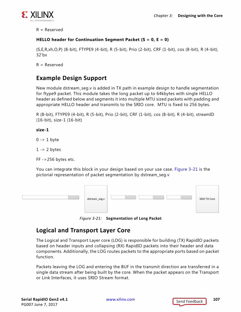
Serial RapidIO Gen2 v4.1 www.xilinx.com 107PG007 June 7, 2017
Chapter 3: Designing with the Core
R = Reserved
HELLO header for Continuation Segment Packet (S = 0, E = 0)
{S,E,R,xh,O,P} (8-bit), FTYPE9 (4-bit), R (5-bit), Prio (2-bit), CRF (1-bit), cos (8-bit), R (4-bit), 32'bx
R = Reserved
Example Design SupportNew module dstream_seg.v is added in TX path in example design to handle segmentation for ftype9 packet. This module takes the long packet up to 64kbytes with single HELLO header as defined below and segments it into multiple MTU sized packets with padding and appropriate HELLO header and transmits to the SRIO core. MTU is fixed to 256 bytes.
R (8-bit), FTYPE9 (4-bit), R (5-bit), Prio (2-bit), CRF (1-bit), cos (8-bit), R (4-bit), streamID (16-bit), size-1 (16-bit)
size-1
0 -> 1 byte
1 -> 2 bytes
FF ->256 bytes etc.
You can integrate this block in your design based on your use case. Figure 3-21 is the pictorial representation of packet segmentation by dstream_seg.v
Logical and Transport Layer CoreThe Logical and Transport Layer core (LOG) is responsible for building (TX) RapidIO packets based on header inputs and collapsing (RX) RapidIO packets into their header and data components. Additionally, the LOG routes packets to the appropriate ports based on packet function.
Packets leaving the LOG and entering the BUF in the transmit direction are transferred in a single data stream after being built by the core. When the packet appears on the Transport or Link Interfaces, it uses SRIO Stream format.
X-Ref Target - Figure 3-21
Figure 3-21: Segmentation of Long Packet
dstream_seg.v SRIO TX Core
Send Feedback
Serial RapidIO Gen2 v4.1 www.xilinx.com 108PG007 June 7, 2017
Chapter 3: Designing with the Core
Request Flows and Packet Arbitration
The Source and Destination ID fields control packet routing through a RapidIO system and, together with the priority, define the transaction request flow. A switch looks at the packet Destination ID and route that particular packet to the port for which that Destination ID is mapped. This mapping is one of the initial steps necessary in the bring up of a RapidIO system.
Many endpoint implementations mask packets based on the Destination ID. The SRIO Gen2 Endpoint does not perform that check. However, hooks are provided to the user design to allow for implementation of this feature if desired. The deviceid output port on the LOG provides you with the current value stored in the Base DeviceID CSR (Offset 0x60). Width of the output port is dependent on the selected system size. By comparing tuser[15:0] on the output port with the Device ID value, you can create a transaction gate for the unlikely occurrence of an errant packet.
A received packet Source ID is necessary to provide a response back to the proper endpoint. Most applications capture a packet incoming Source ID and store it for use as the Destination ID for the generated response. This is the procedure used by the example design. The LOG uses the tuser[31:16] signal from the transmit port as the Source ID for the outgoing packet. By default, the deviceid output is tied back into the tuser[15:0] inputs to ease implementation. When the AXI4-Lite Maintenance interface is used, the LOG swaps the received request Source ID and Destination ID for the response that is issued to the remote device. This functionality prevents a write to the Device ID CSR from creating a response transaction with a different Source/Destination ID pair than that of the corresponding request.
The LOG offering allows statically defined small system (8-bit Device ID) or large system (16-bit Device ID) support. The side effects of this Vivado IDE option are shown in Table 3-9.
Request packets which share a Source ID/Destination ID pair and are of the same priority make up a transaction request flow. RapidIO compliancy dictates that requests of the same transaction request flow do not pass responses of that same flow. For that reason, it is important that when a response is generated, the priority field is bumped by one. Additionally, transactions that solicit responses, such as NWRITE_R transactions, might not be given a priority of 2’b11 to accommodate this priority bump.
Although a request of a priority flow might not pass a response, there is no rule requiring responses to be issued in order. It is entirely possible that read requests are returned out of
Table 3-9: LOG System Size Side Effects
Small System Large System
tt Field for Outgoing Packets 2’b00 2’b01
deviceid Output Port16 bits wide and right justified value from the Base_deviceID field of the Base Device ID CSR
16 bits wide and derived from the Large_base_deviceID field of the Base Device ID CSR
Send Feedback

Serial RapidIO Gen2 v4.1 www.xilinx.com 109PG007 June 7, 2017
Chapter 3: Designing with the Core
order. For this reason, the srcTID (and corresponding targetTID for Response type transactions) field is provided to allow tracking of outstanding request/response pairs. It is up to the user design to track the transaction IDs (TIDs) for each request and correlate them with their responses. It is intended that each Source ID/Destination ID pair has only one outstanding transaction representing each TID value at any one time. As responses are received, the TIDs are freed and you can choose to reissue that TID.
Additionally, the PHY provides a port_timeout output port which reflects the value in the Port Response Time-out Control CSR of the PHY. This value can be used in implementation of a timer to determine if a request/response pair has been outstanding for longer than the specified time frame. By using the TID values, the customer can implement a timer to tag each transaction and take action on a long outstanding transaction. The action taken is beyond the scope of both this document and of the Serial RapidIO Specification [Ref 13].
All transmit ports must share the same transmit path through the BUF and PHY. The LOG arbitrates between the interfaces on a first come, first served basis. If packets are available on multiple ports simultaneously, the LOG selects the port that has been inactive for the longest time. This prevents starvation of any given port. Additionally, the BUF has a respone_only input which restrict the initiator ports from being arbitrated. This signal incorporates the master_enable signal from the PHY, and also asserts when the buffer is filled beyond a certain watermark. In asserting this signal, the BUF forces a path for response transactions to prevent deadlock scenarios.
The Port General Control CSR houses the PHY Master Enable register. By allowing configuration access to this register, the RapidIO Specification allows a single endpoint to act as system host and turn on other endpoints as masters after the system is fully configured. The default value of the Master Enable bit is configurable through the Vivado IDE.
Local Configuration Space Base Address Accesses
As per the RapidIO Specification requirements, the LOG provides a Local Configuration Space Base Address (LCSBA) register in the LOG configuration space. See Local Configuration Space Base Address 1 CSR in Chapter 2 for the register description. For the LOG, usage of this register is limited to bits 30:21. These 10 bits act as a comparison for bits 33:24 of the incoming 34-bit transaction address. If these two 10-bit vectors match for an incoming non-maintenance transaction, it is routed to the Maintenance Port if it exists (otherwise, the packet is handled as a normal I/O transaction).
By default, the LCSBA value is set to 10'h3FF. If left this way, all NREAD and NWRITE transactions with addresses in the range 34’h3_FF00_0000 - 34’h3_FFFF_FFFF are mapped to the maintenance port. It is up to you to find a 16M block of address space outside of the endpoint-used address range to be used as configuration space offset if LCSBA support is enabled in the Vivado IDE.
Note: The RapidIO Specification does not provide for disabling the LCSBA functionality, and it should only be disabled in a closed system.
Send Feedback
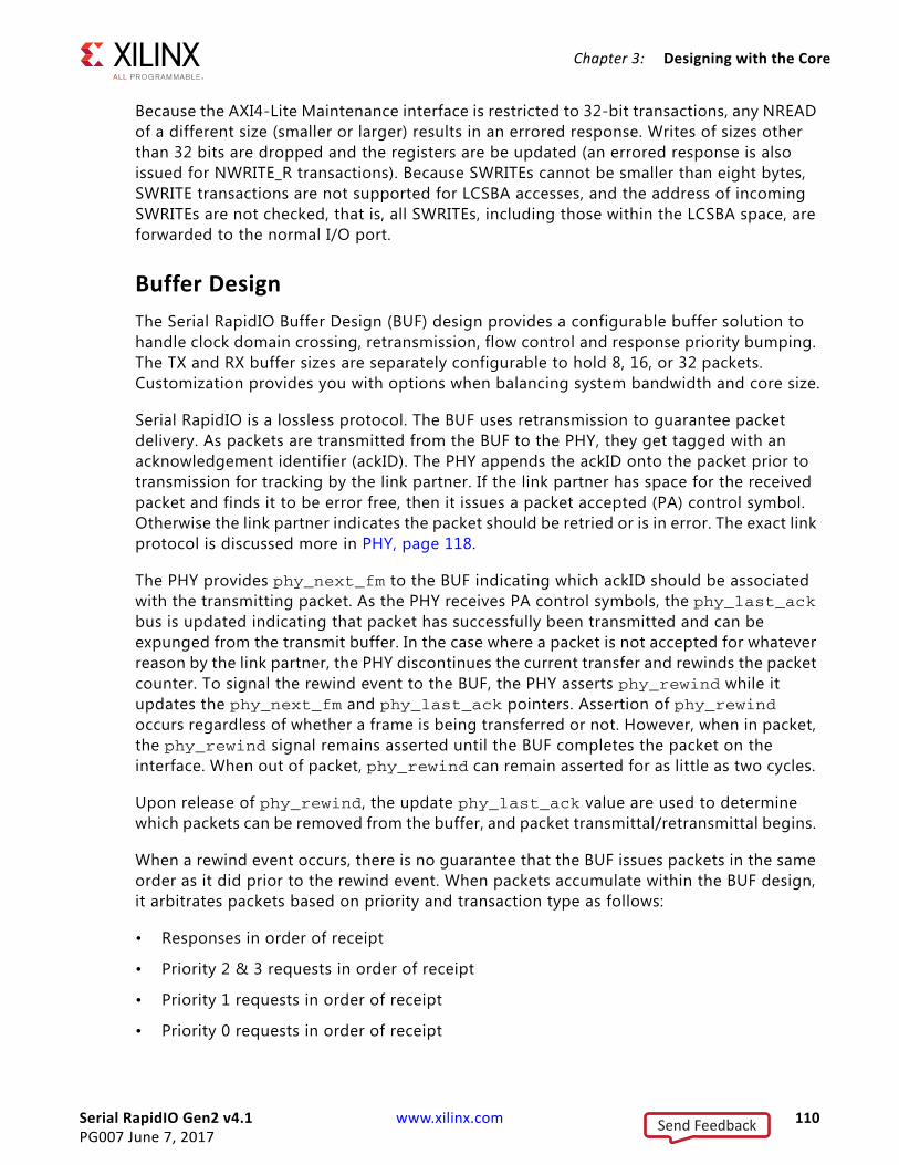
Serial RapidIO Gen2 v4.1 www.xilinx.com 110PG007 June 7, 2017
Chapter 3: Designing with the Core
Because the AXI4-Lite Maintenance interface is restricted to 32-bit transactions, any NREAD of a different size (smaller or larger) results in an errored response. Writes of sizes other than 32 bits are dropped and the registers are be updated (an errored response is also issued for NWRITE_R transactions). Because SWRITEs cannot be smaller than eight bytes, SWRITE transactions are not supported for LCSBA accesses, and the address of incoming SWRITEs are not checked, that is, all SWRITEs, including those within the LCSBA space, are forwarded to the normal I/O port.
Buffer DesignThe Serial RapidIO Buffer Design (BUF) design provides a configurable buffer solution to handle clock domain crossing, retransmission, flow control and response priority bumping. The TX and RX buffer sizes are separately configurable to hold 8, 16, or 32 packets. Customization provides you with options when balancing system bandwidth and core size.
Serial RapidIO is a lossless protocol. The BUF uses retransmission to guarantee packet delivery. As packets are transmitted from the BUF to the PHY, they get tagged with an acknowledgement identifier (ackID). The PHY appends the ackID onto the packet prior to transmission for tracking by the link partner. If the link partner has space for the received packet and finds it to be error free, then it issues a packet accepted (PA) control symbol. Otherwise the link partner indicates the packet should be retried or is in error. The exact link protocol is discussed more in PHY, page 118.
The PHY provides phy_next_fm to the BUF indicating which ackID should be associated with the transmitting packet. As the PHY receives PA control symbols, the phy_last_ack bus is updated indicating that packet has successfully been transmitted and can be expunged from the transmit buffer. In the case where a packet is not accepted for whatever reason by the link partner, the PHY discontinues the current transfer and rewinds the packet counter. To signal the rewind event to the BUF, the PHY asserts phy_rewind while it updates the phy_next_fm and phy_last_ack pointers. Assertion of phy_rewind occurs regardless of whether a frame is being transferred or not. However, when in packet, the phy_rewind signal remains asserted until the BUF completes the packet on the interface. When out of packet, phy_rewind can remain asserted for as little as two cycles.
Upon release of phy_rewind, the update phy_last_ack value are used to determine which packets can be removed from the buffer, and packet transmittal/retransmittal begins.
When a rewind event occurs, there is no guarantee that the BUF issues packets in the same order as it did prior to the rewind event. When packets accumulate within the BUF design, it arbitrates packets based on priority and transaction type as follows:
• Responses in order of receipt
• Priority 2 & 3 requests in order of receipt
• Priority 1 requests in order of receipt
• Priority 0 requests in order of receipt
Send Feedback

Serial RapidIO Gen2 v4.1 www.xilinx.com 111PG007 June 7, 2017
Chapter 3: Designing with the Core
Under normal operating conditions, the SRIO Gen2 Endpoint transmits packets at the same rate they are received so arbitration among packets in the buffer does not come into play. However, when errors occur or buffers begin to fill and flow control comes into play, the BUF begins to back-up and multiple packets must be arbitrated.
IMPORTANT: The arbitration mechanism and its impact on the use model must be taken into account when considering system design issues, such as how to prioritize packets.
If a system generates a steady traffic flow using the SRIO Gen2 Endpoint as initiator, then it is suggested to use the same priority for all request traffic so that no one flow gets starved. However, if a system uses bursts of data within 1 or 2 high priority flows, then a tiered priority methodology might be beneficial because the lower priority flows have lulls of inactivity in which to complete.
Flow Control
The Serial RapidIO Specification [Ref 13] allows for two different forms of flow control, transmitter (TX) and receiver (RX) controlled. The BUF supports both forms. In addition, you can choose to generate an RX-controlled-only buffer which saves on resources, possibly at the expense of bandwidth.
When using receiver controlled flow control, the BUF relies on PHY retry protocol to throttle link traffic. The Serial RapidIO Specification requires that a receive buffer reserve one space per priority jump and 1 space for responses. As the receive buffer fills past these points, it should begin retrying lower priority packets shown in Table 3-10.
When a packet of too low of a priority gets retried, the BUF rewinds the packets it sent by re-queuing everything for arbitration. If the packet which was retried is a response packet, the same packet is reissued; however, the packet priority is increased by one. This is allowed for endpoints by RapidIO protocol to prevent deadlock scenarios where response transactions back up and eventually block the receiver queue. The remaining packets are arbitrated, as shown in Table 3-10.
Table 3-10: Receive BUF Priority Allowance
Available Buffers Remaining Lowest Priority Packet to Be Accepted
4 or more All priorities
3 priorities 1, 2 and 3
2 priorities 2 and 3
1 priority 3 responses only
0 no space, nothing accepted
Send Feedback
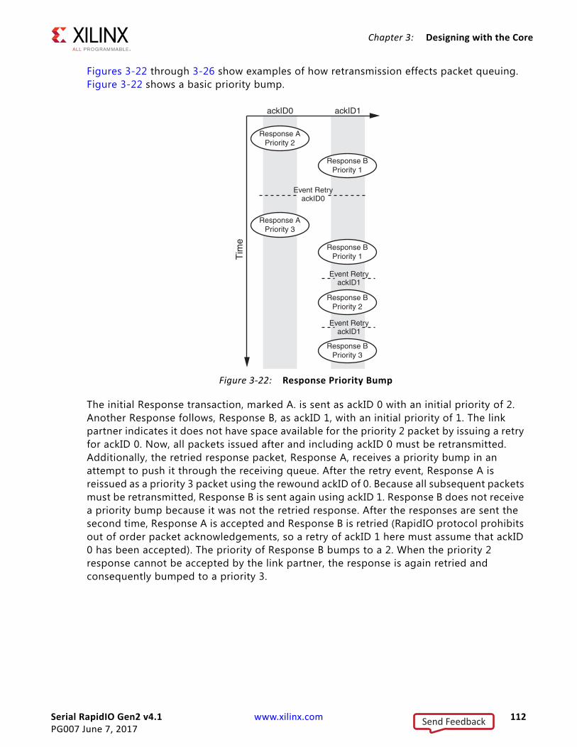
Serial RapidIO Gen2 v4.1 www.xilinx.com 112PG007 June 7, 2017
Chapter 3: Designing with the Core
Figures 3-22 through 3-26 show examples of how retransmission effects packet queuing. Figure 3-22 shows a basic priority bump.
The initial Response transaction, marked A. is sent as ackID 0 with an initial priority of 2. Another Response follows, Response B, as ackID 1, with an initial priority of 1. The link partner indicates it does not have space available for the priority 2 packet by issuing a retry for ackID 0. Now, all packets issued after and including ackID 0 must be retransmitted. Additionally, the retried response packet, Response A, receives a priority bump in an attempt to push it through the receiving queue. After the retry event, Response A is reissued as a priority 3 packet using the rewound ackID of 0. Because all subsequent packets must be retransmitted, Response B is sent again using ackID 1. Response B does not receive a priority bump because it was not the retried response. After the responses are sent the second time, Response A is accepted and Response B is retried (RapidIO protocol prohibits out of order packet acknowledgements, so a retry of ackID 1 here must assume that ackID 0 has been accepted). The priority of Response B bumps to a 2. When the priority 2 response cannot be accepted by the link partner, the response is again retried and consequently bumped to a priority 3.
X-Ref Target - Figure 3-22
Figure 3-22: Response Priority Bump
ackID0 ackID1
Tim
e
Event RetryackID1
Event RetryackID1
Event RetryackID0
Response APriority 2
Response APriority 3
Response BPriority 1
Response BPriority 1
Response BPriority 2
Response BPriority 3
Send Feedback
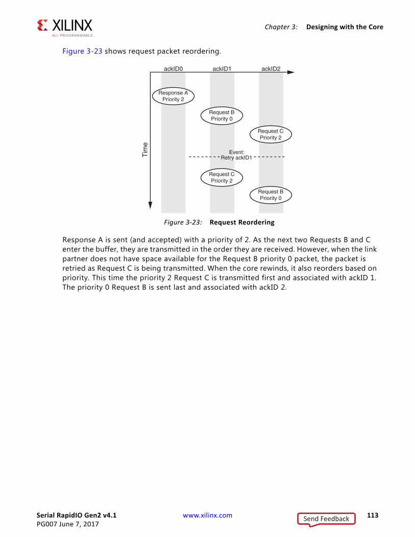
Serial RapidIO Gen2 v4.1 www.xilinx.com 113PG007 June 7, 2017
Chapter 3: Designing with the Core
Figure 3-23 shows request packet reordering.
Response A is sent (and accepted) with a priority of 2. As the next two Requests B and C enter the buffer, they are transmitted in the order they are received. However, when the link partner does not have space available for the Request B priority 0 packet, the packet is retried as Request C is being transmitted. When the core rewinds, it also reorders based on priority. This time the priority 2 Request C is transmitted first and associated with ackID 1. The priority 0 Request B is sent last and associated with ackID 2.
X-Ref Target - Figure 3-23
Figure 3-23: Request Reordering
ackID0 ackID1 ackID2
Tim
eEvent:
Retry ackID1
Response APriority 2
Request BPriority 0
Request CPriority 2
Request CPriority 2
Request BPriority 0
Send Feedback
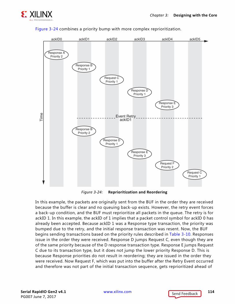
Serial RapidIO Gen2 v4.1 www.xilinx.com 114PG007 June 7, 2017
Chapter 3: Designing with the Core
Figure 3-24 combines a priority bump with more complex reprioritization.
In this example, the packets are originally sent from the BUF in the order they are received because the buffer is clear and no queuing back-up exists. However, the retry event forces a back-up condition, and the BUF must reprioritize all packets in the queue. The retry is for ackID 1. In this example, the ackID of 1 implies that a packet control symbol for ackID 0 has already been accepted. Because ackID 1 was a Response type transaction, the priority was bumped due to the retry, and the initial response transaction was resent. Now, the BUF begins sending transactions based on the priority rules described in Table 3-10. Responses issue in the order they were received. Response D jumps Request C, even though they are of the same priority because of the D response transaction type. Response E jumps Request C due to its transaction type, but it does not jump the lower priority Response D. This is because Response priorities do not result in reordering; they are issued in the order they were received. Now Request F, which was put into the buffer after the Retry Event occurred and therefore was not part of the initial transaction sequence, gets reprioritized ahead of
X-Ref Target - Figure 3-24
Figure 3-24: Reprioritization and Reordering
ackID0 ackID1 ackID2 ackID3 ackID4 ackID5T
ime
Response APriority 2
Response BPriority 1
Request CPriority 1
Response DPriority 1
Response EPriority 3
Response BPriority 2
Response DPriority 1
Response EPriority 3
Request FPriority 2
Request CPriority 1
Event RetryackID1
Send Feedback
Serial RapidIO Gen2 v4.1 www.xilinx.com 115PG007 June 7, 2017
Chapter 3: Designing with the Core
Request C due to its higher priority value. Request C issues last due to its low priority value and Request transaction type.
If a link partner has a small buffer, the buffer fills and empty faster. This means that the retry scenarios which govern RX flow control happen more frequently and those small buffers can run dry during retry recovery, particularly if packets sizes are small. Additionally, some major RapidIO vendors do not support transmitter controlled flow control. When interfacing to one of these vendors, generate a receiver controlled only core to optimize resource usage. It is also suggested to increase the buffer sizes to reduce the risk of dry and overrun buffers.
Transmitter controlled flow control is meant to keep link bandwidth up by limiting rewind scenarios. The BUF provides you with a programmable watermark register (CSR 0x10004). This register carries each of the three watermark values used to determine when to block lower priority packets as the link partner buffer space fills.
RECOMMENDED: Write this register in its entirety to maintain valid watermark configurations (0 < WM2 < WM1 < WM0).
The BUF bases packet transmittal decisions on a combination of status updates from the link partner (phy_rcvd_buf_stat), outstanding packet count (phy_next_fm - phy_last_ack - 1) and the internal watermark values. The BUF still sends packets in the order detailed in Table 3-10, but it does not send lower priority packets if the available buffer space falls below the watermark value for the packet. Additionally, response priorities are automatically adjusted based on the calculated buffer space available (phy_rcvd_buf_stat - (phy_next_fm - phy_last_ack - 1)).
Send Feedback
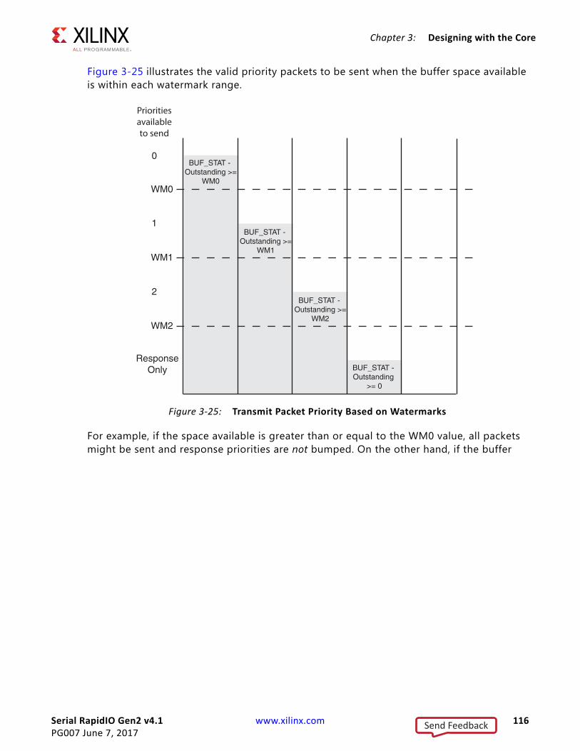
Serial RapidIO Gen2 v4.1 www.xilinx.com 116PG007 June 7, 2017
Chapter 3: Designing with the Core
Figure 3-25 illustrates the valid priority packets to be sent when the buffer space available is within each watermark range.
For example, if the space available is greater than or equal to the WM0 value, all packets might be sent and response priorities are not bumped. On the other hand, if the buffer
X-Ref Target - Figure 3-25
Figure 3-25: Transmit Packet Priority Based on Watermarks
WM2
WM1
WM0
ResponseOnly
2
1
0BUF_STAT -
Outstanding >=WM0
BUF_STAT - Outstanding >=
WM1
BUF_STAT - Outstanding >=
WM2
BUF_STAT - Outstanding
>= 0
Prioritiesavailableto send
Send Feedback
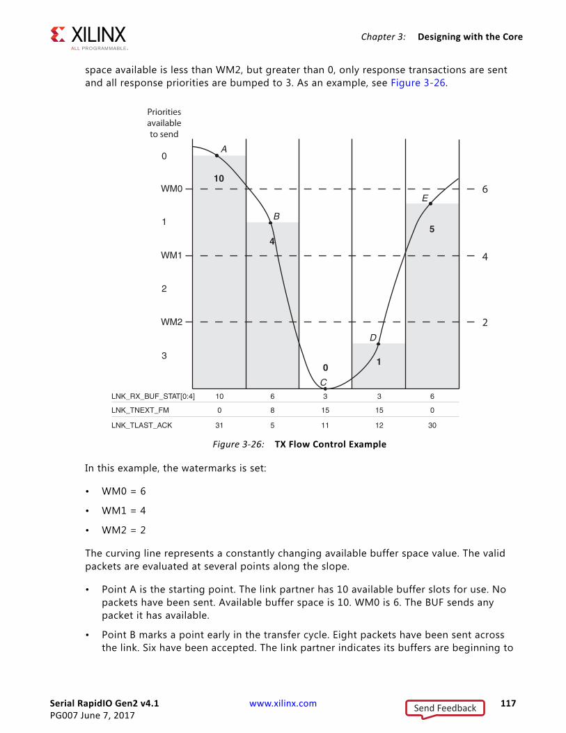
Serial RapidIO Gen2 v4.1 www.xilinx.com 117PG007 June 7, 2017
Chapter 3: Designing with the Core
space available is less than WM2, but greater than 0, only response transactions are sent and all response priorities are bumped to 3. As an example, see Figure 3-26.
In this example, the watermarks is set:
• WM0 = 6
• WM1 = 4
• WM2 = 2
The curving line represents a constantly changing available buffer space value. The valid packets are evaluated at several points along the slope.
• Point A is the starting point. The link partner has 10 available buffer slots for use. No packets have been sent. Available buffer space is 10. WM0 is 6. The BUF sends any packet it has available.
• Point B marks a point early in the transfer cycle. Eight packets have been sent across the link. Six have been accepted. The link partner indicates its buffers are beginning to
X-Ref Target - Figure 3-26
Figure 3-26: TX Flow Control Example
WM2
WM1
WM0
3
2
1
0
Prioritiesavailableto send
6
4
2
LNK_RX_BUF_STAT[0:4]
LNK_TNEXT_FM
LNK_TLAST_ACK
10 6 3 3 6
0 8 15 15 0
31 5 11 12 30
10
4
01
5
A
B
C
D
E
Send Feedback
Serial RapidIO Gen2 v4.1 www.xilinx.com 118PG007 June 7, 2017
Chapter 3: Designing with the Core
fill. Now the BUF sees four available slots. Because that is equal to WM1, priority 0 packets are no longer transmitted. All priority 0 requests queue in the buffer.
• At point C, the link partner indicates it has only a few spaces left. The endpoint has not received acknowledgment for three of its outstanding packets. The BUF must stop transmission of packets until it receives indication that buffer spaces have become available.
• At point D, the BUF has received an additional acknowledgement lowering the outstanding packet count by one without a change in the buf_status. Because 1 space is available, the BUF is able to send a response. It bumps the response priority to 3 to ensure acceptance.
• At point E, the link partner buffer has become more available, reporting a buffer status of six. Because the BUF has only one outstanding packet, it is able to send any transaction except a priority 0 request.
In Figure 3-26, after the available buffer count drops below watermark 0, priority 0 request packets begin to accumulate in the buffer. As the available buffer space continues to drop past point B, priority 1 requests start to queue in the buffer. The buffer accumulates these packets and it is likely that eventually, it asserts the response_only output. Now, only response type transactions are accepted into the buffer until some of the lower priority packets get cleared out. Unless the system has constantly streaming responses, this creates windows of lower priority traffic. Smaller transmit buffers force those windows on a more frequent basis; however, they are also more likely to incur bandwidth penalties because RX buffers could run dry in the buffer status turn-around time. This is particularly true when smaller packets are transferred.
The receive side of the buffer queues packets as first-in-first-out. As each packet comes in, the BUF checks the priority to see if space is available. Receive side availability is governed by hard watermarks ensuring that there is one space available for each allowed priority level, as shown in Table 3-10, page 111.
The configurable read buffer size gives system designers the ability to make trade-offs between bandwidth and resources. The smaller buffer provides a LUT savings at the expense of potentially reduced bandwidth. Small and medium size packets quickly fill the 8 deep buffer and incur retries and TX flow control throttling. Asynchronous clocking implementations exacerbate the situation due to latencies inherent to domain crossing logic.
PHYThis section describes the functionality within the Serial RapidIO PHY, including communication with the core through the Link Interface. This section also describes initializing the RapidIO link, managing control symbols, receiving and transmitting data packets, issuing and responding to discontinues, managing the acknowledgement identifiers, detecting special case error conditions, setting up timeout counters, and receiving and transmitting multicast event control symbols.
Send Feedback
Serial RapidIO Gen2 v4.1 www.xilinx.com 119PG007 June 7, 2017
Chapter 3: Designing with the Core
Initializing the RapidIO Link
The PHY must be initialized and aligned so that data packets and control symbols can be reliably received. The PHY goes through initialization and alignment after reset and recovers the incoming data and clock from the input serial stream.
Initialization and alignment occurs when coming out of reset or after loss of sync on the input port during system operation. Guidelines for initialization and alignment can be found in the RapidIO Interconnect Specification - Part VI: Physical Layer 1x/4x LP-Serial Specification [Ref 14].
Monitor the following signals to monitor whether the link is initialized and aligned:
• port_initialized: Link has locked to receive stream.
• mode_1x: For a 2x or 4x core, signal indicates that the core has trained down to one lane. This is valid after port_initialized asserts.
• rx_lane_r: Indicates that the core has trained to the redundancy lane.
• idle2_selected: Indicates that the core is operating in IDLE2 mode.
• out_of_sync: Indicates that the scrambler is not synchronized (only valid when scrambling is enabled).
• link_initialized: Indicates seven consecutive error free control symbols have been received and 15 consecutive symbols have been sent. The core is fully trained and can now transmit data.
These signals can be used to determine when the PHY TX and RX serial links are operational. The PHY interface can then start receiving and transmitting packets.
Management of Control Symbols
Incoming control symbols are consumed by the PHY and are not passed on to the user application. The PHY processes control symbols, and if necessary, responds with an appropriate control symbol response. To illustrate, if the PHY receives an incoming link request control symbol, it responds by automatically generating link response control symbols on the transmit port.
Table 3-11 contains the SRIO control symbols and the actions taken by the PHY. The transmit action describes the conditions when the PHY would transmit the control symbol. The receive action describes the action taken by the core when receiving the particular control symbol. For more information on SRIO defined control symbols, see the RapidIO Interconnect Specification - Part VI: Physical Layer 1x/4x LP-Serial Specification [Ref 14].
Send Feedback

Serial RapidIO Gen2 v4.1 www.xilinx.com 120PG007 June 7, 2017
Chapter 3: Designing with the Core
Table 3-11: SRIO Physical Layer Control Symbols
Control Symbol Transmit Action Receive Action
Packet Accepted (PA) Transmits PA control symbol when the BUF accepts a packet on the link receive interface.
Updates phy_last_ack output so that the BUF can release the acknowledged packet.
Packet Not Accepted (PNA) Transmits PNA control symbol when the PHY detects an error condition on the incoming packet buffer. Discards all incoming data until a LR_IS control symbol is received.
Stops transmission of outbound data and transmits a LR_IS control symbol to the connected device. Asserts phy_rcvd_pna for one clock cycle. Asserts phy_rewind output until the Link Response handshake is complete at which point phy_next_fm is updated with the next expected packet and phy_last_ack is updated to phy_next_fm-1.
Packet Retry (PR) Transmits PR control symbol when the BUF is not accepting packets on the link receive interface and the internal buffer storage has been exhausted.
Updates phy_next_fm output to the BUF with ackID of retried packet and asserts phy_rewind, indicating a retransmission is necessary and transmits a RFR control symbol.
Stomp (STMP) Inserts STMP control symbol when BUF terminates a packet by asserting a phyr_tlast and phyr_tuser[0].
Discontinues packet to the BUF by asserting phyr_tlast and phyr_tuser[0] to indicate a bad packet. Transmits PR to the sending device.
Status (STAT) Receives STAT control symbols after every 1024 code groups.
Updates the phy_rcvdbuf_stat to the BUF with the buf_status value in the STAT control symbol.
Link Request - Input Status (LR_IS)
Transmits LR_IS when a PNA is received or other detected protocol violation. Monitors RX port for incoming LRESP control symbol.
Receives LRESP control symbol with the next expected ackID value and looks for next incoming packet ackID value to equal the expected ackID value.
Link Response (LRESP) Transmits LRESP control symbols when receiving a LR_IS control symbol. Transmits the next expected ackID value by the BUF on the link receive interface.
Updates the phy_last_ack and/or phy_next_fm bus with the incoming ackID value in the LRESP. This signals the BUF to release and retry packets.
Link Request - Reset Device (LR_RD)
Transmits LR_RD control symbols when the phy_link_reset signal is asserted. It needs to be asserted until the port_initialized signal goes Low to successfully reset the opposite end of the link. Control symbols that are in process may get masked by assertion of this signal.
Asserts phy_rcvd_link_reset to indicate that the core has received four LR_RD control symbols. The PHY is also reset.
Send Feedback

Serial RapidIO Gen2 v4.1 www.xilinx.com 121PG007 June 7, 2017
Chapter 3: Designing with the Core
Link Reset
You should monitor the phy_rcvd_link_reset signal, which indicates that the PHY has received four Link Request Reset Device control symbols and is resetting the core. All states must return to their default value. Depending on the application implementation of sys_rst, sys_rst can be asserted in response to the assertion of phy_rcvd_link_reset to reset the entire application.
Driving the Receive BUF Status
The receive buffer status, phy_buf_stat[5:0], is a six-bit signal that is buffer-driven to the PHY. The BUF typically stores the incoming packets in a block RAM. This signal indicates the number of maximum-sized packets that the BUF can accommodate. The encoding value specifies the number of packet buffers currently available. This could represent anywhere from 0 (6’b00_0000) to 30 (6’b01_1110) available buffers. This information is encoded in the buf_status field of the outgoing acknowledgement, status and packet retry control symbols issued by the PHY.
Based on the previous information, the connected device decides whether it can transmit more packets to the PHY. If the BUF has no available buffers for packets (phy_buf_stat[5:0]= 6’b00_0000), it discontinues incoming packets. Doing so causes the PHY to send out a packet-retry control symbol to the sender and to discard all incoming packets.
If not using a standard RapidIO buffer, a minimum of one buffer must be implemented to store a full size packet. In this case, dynamically drive just the least significant bit of the phy_buf_stat[5:0] signal. All other unused bits of the phy_buf_stat[5:0] signal are
Start of Packet (SOP) Inserts SOP on all outbound packets. When possible, the core transmits SOP control symbol to indicate a end of one packet and a start of another packet.
Strips incoming stream of SOP control symbol and uses SOP control symbol to mark the beginning of a packet.
End of Packet (EOP) Inserts EOP at the end of an outbound packet if necessary.
Strips incoming stream of EOP control symbol and uses EOP control symbol to mark the end of a packet.
Restart from Retry (RFR) Transmits RFR control symbol when PHY receives a PR control symbol. The phy_next_fm bus indicates that the BUF must retry a packet.
Strips incoming stream of RFR control symbol and looks for next packet ackID value to equal the expected ackID value.
Multi-cast Event (MCE) If user asserts phy_mce, transmits MCE control symbol.
Asserts phy_rcvd_mce when the core receives an MCE control symbol.
Table 3-11: SRIO Physical Layer Control Symbols (Cont’d)
Control Symbol Transmit Action Receive Action
Send Feedback
Serial RapidIO Gen2 v4.1 www.xilinx.com 122PG007 June 7, 2017
Chapter 3: Designing with the Core
tied to ground. A value of 0 indicates no buffers available, and a 1 would mean that the device has one empty buffer.
If receiver based flow control is needed, tie phy_buf_stat[5:0]= 6’b11_1111.
Stripping the Final CRC in Received User-Defined Packets
RapidIO packets greater than 80 bytes contain both an intermediate and final CRC. RapidIO packets 80 bytes or less contain only the final CRC. When present, the intermediate CRC is stripped from the packet. The final CRC is also stripped in most cases. However, the RapidIO Specification allows for 16 bits of zero padding in addition to the final CRC. In the case of user-defined packet types, the PHY strips the last 16 bits of the packet but if the zero padding is used, the CRC is still part of the packet passed to the BUF.
Interpreting the Transmit BUF Status
The transmit buffer status, phy_rcvd_buf_stat[5:0], is a six-bit signal driven by the PHY to the BUF. It indicates the number of maximum-sized packets that the connected remote device can accommodate. The encoding value specifies the number of packet buffers the remote device has currently available, and could represent anywhere from 0 (6’b00_0000) to 30 (6’b1_1110) available buffers in IDLE1 operation, or from 0 (6'b00_0000) to 62 (6'b11_1110) in IDLE2 operation. This information is encoded in the buf_status field of incoming acknowledgement, status and packet retry control symbols issued by the remote PHY.
Based on the preceding information, the buffer application design can implement transmitter based flow control logic and decide whether it can transmit more packets to the connected devices.
If the phy_rcvd_buf_stat[5:0] = 6’b11_1111, the connected devices use receiver-based flow control.
Acknowledgement Identification
The following signals are provided by the PHY to the BUF in relation to the Acknowledgement Identifier, ackID.
• phy_last_ack[5:0]
• phy_next_fm[5:0]
The details of the preceding signals are provided in Managing the Transmit Acknowledgement Identification, page 124.
Send Feedback
Serial RapidIO Gen2 v4.1 www.xilinx.com 123PG007 June 7, 2017
Chapter 3: Designing with the Core
Discontinues in the Physical Layer
Discontinues are used if either the BUF or the PHY wants to discontinue data transfer due to unavailability of resources, FIFO overflows, internal conditions, or CRC errors.
This section describes PHY and BUF signals for indicating discontinues in the receive and transmit paths. The operation of the discontinues, their possible causes and effects are also provided.
Link Receive Source Discontinue
Operation
The PHY sets the discontinue bit in m_axis_phyr_tuser (bit 0) along with m_axis_phyr_tlast to indicate that it wants to discontinue data transfer to the BUF. Upon taking this action, the PHY stops the transfer of the packet.
• Cause: This discontinue signal is asserted by the PHY if a CRC error is detected, the packet is stomped, or other error conditions during the packet reception cause this signal to be asserted.
• Effect: When this signal is asserted, data transfer between the BUF and the PHY stops. The core stops the transfer of the packet and if necessary, transmits a packet-not-accepted control symbol or a packet retry to the sender of the packet. If the BUF receives any portion of the packet when the discontinue is asserted, the BUF is responsible for discarding the packet.
Link Receive Destination Discontinue
Operation
The BUF cannot discontinue a packet in the receive direction.
Link Transmit Source Discontinue (Rewind)
Operation
The BUF sets the discontinue bit in m_axis_phyt_tuser (bit 0) along with m_axis_phyt_tlast to indicate a desire to discontinue data transfer to the PHY.
• Cause: This discontinue signal is asserted when a rewind scenario occurs, as indicated by phy_rewind.
• Effect: When this signal is asserted, data transfer between the BUF and the PHY stops. The PHY do not increase the phy_next_fm, resulting in retransmission of the packet by the user design. If a part of the packet has already been sent by the PHY to the RapidIO fabric when the discontinue was asserted, the PHY cancels the packet by issuing a stomp control symbol.
Send Feedback
Serial RapidIO Gen2 v4.1 www.xilinx.com 124PG007 June 7, 2017
Chapter 3: Designing with the Core
Link Transmit Destination Discontinue
Operation
The PHY asserts the phy_rewind signal to indicate that it wants to discontinue data transfer from the BUF. Upon assertion of this signal, the PHY stops receiving the packet. The phy_rewind signal should remain asserted until the buffer signals the end of the packet by asserting m_axis_phyt_tlast.
• Cause: The PHY asserts this discontinue if it has entered the output port error recovery process because it has received a packet-not-accepted control symbol or has entered the output retry-stopped recovery process because it has received a packet retry control symbol.
• Effect: When this signal is asserted, data transfer between the BUF and the PHY stops. The core changes the lnk_tnext_fm to the packet that needs to be sent, resulting in retransmission of the packet by the BUF application.
Managing the Transmit Acknowledgement Identification
The acknowledge ID (ackID) is an identifier used for acknowledgement of packets transmitted across a link. In IDLE2 mode (when long control symbols are in use), the ackID has six significant bits and allows for a range of up to 63 outstanding unacknowledged packets. In IDLE1 mode (when short control symbols are in use), bit 0 is tied to zero, and allow for up to 31 outstanding unacknowledged packets.The ackIDs are assigned sequentially, in an increasing order, wrapping back to zero on overflow, to indicate the order of packet transmission. They are sent out to the RapidIO fabric as a Physical Layer header field in the transmit packet.
The following signals facilitate management of the ackIDs on the Link Transmit interface:
• phy_last_ack[5:0]: This signal indicates the last valid (expected) packet acknowledgement that was received by the PHY. The BUF can then release the frame whose acknowledgment was received for reuse. However, if there was an error with acknowledgement control symbol with the ackID, this signal remains unchanged.
• phy_next_fm[5:0]: This signal indicates the ackID of the next packet to be transmitted if the transmit link is idle. It might also denote the ackID of the packet currently being transmitted. However, if the interface gets a retry due to an error in the packet sent out, this signal remains unchanged. The BUF must also correlate this value to the packet that is currently being transmitted.
Normal Operation
During normal operation, the BUF must associate all transmit packets with the value being presented on phy_next_fm. This is the ackID value that is transmitted in the physical layer header fields of that packet. After the connected device acknowledges the packet, it transmits a packet accepted control symbol with the ackID value equal to the ackID value
Send Feedback
Serial RapidIO Gen2 v4.1 www.xilinx.com 125PG007 June 7, 2017
Chapter 3: Designing with the Core
found in the accepted packet. The PHY updates phy_last_ack with the ackID value found in the packet accepted control symbol. Based on this update, the BUF then releases the buffer location that is holding this packet.
Error Recovery Operation
This section describes scenarios that you must be aware of during error recovery. These cases illustrate the conditions causing the BUF to retransmit a packet or acknowledge one or several packets simultaneously.
Scenario 1: Packet Retry Due to Internal Condition
The connected device retries a packet due to some temporary internal condition.
Effect: After a packet retry control symbol is received, the PHY discontinues the BUF on the link transmit interface. The core transmits a restart-from-retry control symbol. The core also updates the phy_next_fm with the ackID value received in the packet retry control symbol. This indicates that the BUF must start retransmitting packets from that ackID value, thereby reestablishing the proper ordering between the devices. If the retry control symbol is received with an ackID value equal to the current phy_next_fm, that is, phy_next_fm does not increase, and the BUF must retry the packet that was discontinued.
Scenario 2: Handling Out-of-Sequence ackIDs
The PHY transmits packets with ackIDs in a sequence, and it receives acknowledgements for all but an earlier ackID. This indicates a possible error with the packet of the ackID not received.
Effect: The PHY discontinues the BUF on the link transmit interface. It then transmits a link request input status control symbol. After the connected device receives the link request input status control symbol, it transmits a link response control symbol, indicating which packet ackID it expects to receive next. These actions might need to be taken based on the link response ackID value:
• The Link Response ackID field indicates that the connected device has acknowledged one or more ackIDs greater than what was currently being driven on phy_last_ack. The PHY updates phy_last_ack with the value in the link response control symbol. The BUF can release all buffer locations starting from the previous value of phy_last_ack to the updated value of phy_last_ack.
• The Link Response ackID field indicates that the connected device is expecting a packet with an ackID that was already transmitted. The PHY updates the phy_next_fm with the this value. The BUF must retransmit this packet to re-establish the proper ordering among devices.
Scenario 3: Device Receives Corrupt Control Symbol
The connected device receives a corrupt control symbol from the PHY.
Send Feedback
Serial RapidIO Gen2 v4.1 www.xilinx.com 126PG007 June 7, 2017
Chapter 3: Designing with the Core
Effect: The connected device sends a packet-not-accepted control symbol to the sender. The PHY responds in a similar manner as described in Scenario 2: Handling Out-of-Sequence ackIDs.
Detecting Special Case Error Conditions
The PHY is designed to handle most error conditions as outlined by the RapidIO 1x/4x LP-Serial Specification. However, the following signals must be monitored to avoid system lockup:
• phy_link_reset: Send Link Reset
• phy_rcvd_link_reset: Link Issued Link Reset Control Symbol
• rcvd_pna: Link Packet Not Accepted Received
• port_error: Link Port Error
• force_reinit: Force Reinitialization
Scenario 1: Link Request Reset Device
The link received a Link Request Reset Device. The connected device might issue a link request reset device control symbol sequence. Upon receiving four consecutive link request reset device control symbols, the PHY resets itself and asserts phy_rcvd_link_reset to the user application.
The behavior of the user application on the assertion of phy_rcvd_link_reset is implementation-specific and beyond the scope of this document.
RECOMMENDED: Xilinx recommends that the user application dissociate all ackIDs with the stored packets.
After reset, the PHY drives phy_next_fm to 6’b00_0000, and phy_last_ack to 6'b01_1111 in IDLE1 mode and 6'b11_1111 in IDLE2 mode.
Scenario 2: Fatal Error Conditions
There are some cases where the core detects a fatal error as defined by the RapidIO 1x/4x LP-Serial Specification. This can be, but not necessarily limited to:
• Link Response Timed Out: The PHY transmitted a link request control symbol but no link response control symbol was received.
• Link Response Misaligned AckID Value: A link response ackID field contains a value that is not outstanding.
When these conditions are detected, the core asserts port_error. This signal indicates that the PHY has shut down transmission and reception of packets. You must assert sys_rst to the core to re-initialize the link and reset the error recovery state machines.
Send Feedback
Serial RapidIO Gen2 v4.1 www.xilinx.com 127PG007 June 7, 2017
Chapter 3: Designing with the Core
Scenario 3: Repeated Reception of Packet-Not-Accepted without Progress
A core can have repeated reception of packet-not-accepted without forward progress. When an error is detected during link operation, the connected device issues a packet-not-accepted control symbol. The PHY issues a link request control symbol. The connected device responds with a link response control symbol containing the next expected ackID. The PHY retransmits that packet, and link operation is resumed. However, due to internal error conditions or unreliable link operation, its possible that the connected device continues to transmit a packet not accepted control symbol forcing the link to never make forward progress on packet transmission.
The PHY is designed to facilitate detection of this scenario and to allow you to react based on system and design requirements. Every time a packet not accepted control symbol is received, the rcvd_pna signal asserts for one clock cycle. This signal, combined with the phy_next_fm and phy_last_ack, allows detection of multiple packet-not-accepted control symbols being received without forward progress on packet transmission. This could indicate a serious physical link issue or another system issue. The behavior of the user application on detection of this scenario is beyond the scope of this document and is implementation-specific.
Possible options to implement include:
• Force re-initialization of link by asserting force_reinit.
• Reset the PHY by asserting sys_rst.
• Reset the connected device by asserting phy_link_reset.
Note: Asserting reset to the PHY or to the connected device causes the two devices to either be misaligned on ackID tracking (a fatal error), or to retransmit previously transmitted data, which can result in greater system errors. It is best that if one device is reset, the other be reset too. For example, if a reset is issued to the connected device (using phy_link_reset), the link is re-initialized, and the link_initialized signal deasserts until the link is reestablished.
RECOMMENDED: Xilinx recommends that the user application assert sys_rst to the PHY at that time, thereby forcing all ackID tracking to return to reset values. This prevents any further fatal or system error conditions.
Timeout Counters for Lost Packet Detection
Timeout counters expire when sufficient time has elapsed without receiving the expected response from the system. These are used to detect errors such as a lost response or request packets. The timeout counter value is defined in the Physical Layer Maintenance Command and Status Register (CSR) space as given in the following:
• Port Link Time-out Control CSR (Block Offset 0X 20 Word 0): The port link timeout control register contains the timeout value for link events such as sending a packet to receiving the corresponding acknowledge, and sending a link-request to receiving the corresponding link-response. The reset value (the maximum timeout interval) is
Send Feedback
Serial RapidIO Gen2 v4.1 www.xilinx.com 128PG007 June 7, 2017
Chapter 3: Designing with the Core
user-specified in the Vivado IDE. The max value represents approximately 3 seconds. The value scales linearly from 0 to max. The PHY uses this timeout value to control internal counters that detect error conditions and initiate error recovery or indicate fatal error on port_error.
• Port Response Time-out Control CSR (Block Offset 0X 20 Word 1): The port response timeout control register contains the timeout value for link events such as sending a packet to receiving the corresponding response packet. The reset value (the maximum timeout interval) is user-specified in the Vivado IDE. A value of all ones should correspond to a timeout of between 3 and 6 seconds. The user application is responsible for detection of lost response packets. This timeout value in the CSR is presented to you through the output port port_timeout.
TIP: If you set the default value for the Port Response timeout appropriately during core generation, the Port Link Time-out Counter attempts recovery prior to a Port Response time-out.
Transmitting and Receiving Multicast Event Control Symbols
This section describes how to transmit and receive multicast event control symbols.
Multicast Event Request
Operation
The phy_mce signal is used to request transmission of a multicast event control symbol by the user application.
• Cause: Allows the occurrence of a user-defined system event to be multicast throughout a system.
• Effect: When this signal is asserted, it results in the transmission of a multicast event control symbol by the PHY. This signal should be asserted for one clock cycle.
Multicast Event Decode
Operation
This multicast event decode signal (phy_rcvd_mce) is asserted by the PHY when it has decoded a multicast event control symbol received on the serial link.
• Cause: The PHY has decoded a multicast event control symbol it received.
• Effect: The PHY informs the user application that it has decoded the multicast event control symbol. As multicast events are system specific, the user must determine how to interpret the reception of a multicast event.
Send Feedback
Serial RapidIO Gen2 v4.1 www.xilinx.com 129PG007 June 7, 2017
Chapter 4
Design Flow StepsThis chapter describes customizing and generating the core, constraining the core, and the simulation, synthesis and implementation steps that are specific to this IP core. More detailed information about the standard Vivado® design flows and the IP integrator can be found in the following Vivado Design Suite user guides:
• Vivado Design Suite User Guide: Designing IP Subsystems using IP Integrator (UG994) [Ref 4]
• Vivado Design Suite User Guide: Designing with IP (UG896) [Ref 3]
• Vivado Design Suite User Guide: Getting Started (UG910) [Ref 5]
• Vivado Design Suite User Guide: Logic Simulation (UG900) [Ref 7]
Customizing and Generating the CoreIf you are customizing and generating the core in the Vivado IP integrator, see the Vivado Design Suite User Guide: Designing IP Subsystems using IP Integrator (UG994) [Ref 4] for detailed information. IP integrator might auto-compute certain configuration values when validating or generating the design. To check whether the values do change, see the description of the parameter in this chapter. To view the parameter value you can run the validate_bd_design command in the Tcl Console.
You can customize the IP for use in your design by specifying values for the various parameters associated with the IP core using the following steps:
1. In the IP catalog, expand the categories Standard Bus Interface > RapidIO or Communications & Networking > Wireless.
2. Double-click the selected IP, or select the Customize IP command from the toolbar or right-click menu .
For details, see the Vivado Design Suite User Guide: Designing with IP (UG896) [Ref 3] and the Vivado Design Suite User Guide: Getting Started (UG910) [Ref 5].
Note: Figures in this chapter are illustrations of the Vivado Integrated Design Environment (IDE). This layout might vary from the current version.
Send Feedback
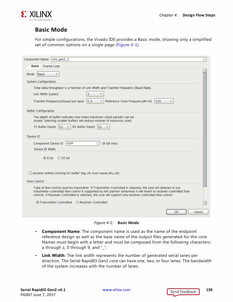
Serial RapidIO Gen2 v4.1 www.xilinx.com 130PG007 June 7, 2017
Chapter 4: Design Flow Steps
Basic ModeFor simple configurations, the Vivado IDE provides a Basic mode, showing only a simplified set of common options on a single page (Figure 4-1).
• Component Name: The component name is used as the name of the endpoint reference design as well as the base name of the output files generated for the core. Names must begin with a letter and must be composed from the following characters: a through z, 0 through 9, and “_”.
• Link Width: The link width represents the number of generated serial lanes per direction. The Serial RapidIO Gen2 core can have one, two, or four lanes. The bandwidth of the system increases with the number of lanes.
X-Ref Target - Figure 4-1
Figure 4-1: Basic Mode
Send Feedback
Serial RapidIO Gen2 v4.1 www.xilinx.com 131PG007 June 7, 2017
Chapter 4: Design Flow Steps
• Transfer Frequency: The transfer frequency represents the per-lane baud rate of the Serial RapidIO core. Each serial transceiver runs at the selected line rate. The bandwidth of the system increases with transfer frequency.
• Reference Clock Frequency: The reference clock frequency is the rate of the clock that is brought into the FPGA on the dedicated transceiver reference clock pins.
• Buffer Configuration: The depth of the transmit and receive buffers can be customized to 8, 16, or 32. This number represents the amount of packets the buffer is capable of storing. Selecting the smaller buffer depths conserves resources (primarily block RAMs and LUTs), whereas maximum buffer depth yields maximum throughput.
• Component Device ID: The Component Device ID determines the reset value for the Base Device ID CSR.
• Device ID Width: The Device ID width of the core should match that of the link partner. Otherwise, transactions can be misinterpreted due to the header shift. Most systems use 8-bit Device IDs, but the SRIO Gen2 Endpoint also provides large system support through this option.
• Silicon Revision: The silicon revision is used to provide the correct components in the example design to match the silicon requirements.
• Unified Clock: Check this box if the user design uses the same clock for log_clk (primary user clock) and phy_clk. Selecting this option significantly reduces both latency and resource utilization.
• Flow Control: These options indicate the type of flow control to be used by the transmitter.
° Transmitter Controlled: Selecting this option causes the core to first attempt to use transmitter-controlled flow control, but switches to receiver-controlled if the link partner does not support it. Transmitter-controlled flow control minimizes retry conditions through the use of received buffer status and watermarks. Receiver-controlled flow control blindly transmits packets and uses the retry protocol.
° Receiver Controlled: Select this option for receiver-controlled flow control only. In this mode, packets are blindly transmitted and the retry protocol is used to control packet flow.
• Additional transceiver control and status ports: Check this box to enable additional transceiver control and status ports. These ports correspond to a transceiver port of the same name in the appropriate device GTX/GTP user guide. These ports are useful when debugging transceiver links.
Send Feedback

Serial RapidIO Gen2 v4.1 www.xilinx.com 132PG007 June 7, 2017
Chapter 4: Design Flow Steps
Advanced ModeThe Advanced mode includes all configuration options.
Basic Tab
Figure 4-2 shows the Basic tab of the Advanced mode.
• Component Name: The component name is used as the name of the endpoint reference design as well as the base name of the output files generated for the core. Names must begin with a letter and must be composed from the following characters: a through z, 0 through 9, and “_”.
• System Configuration
X-Ref Target - Figure 4-2
Figure 4-2: Advanced Mode: Basic Tab
Send Feedback
Serial RapidIO Gen2 v4.1 www.xilinx.com 133PG007 June 7, 2017
Chapter 4: Design Flow Steps
° Link Width: The link width represents the number of serial lanes per direction that are generated. The Serial RapidIO Gen2 core can have one, two, or four lanes. The bandwidth of the system increases with the number of lanes.
° Transfer Frequency: The transfer frequency represents the per-lane baud rate of the Serial RapidIO core. Each serial transceiver runs at the selected line rate. The bandwidth of the system increases with transfer frequency.
° Reference Clock Frequency: The reference clock frequency is the rate of the clock that is brought into the FPGA on the dedicated transceiver reference clock pins.
• Buffer Configuration: The depth of the transmit and receive buffers can be customized to 8, 16, or 32. This number represents the amount of packets the buffer is capable of storing. Selecting the smaller buffer depths conserves resources (primarily block RAMs and LUTs), whereas maximum buffer depth yields maximum throughput.
• Device ID
° Component Device ID: The Component Device ID determines the reset value for the Base Device ID CSR.
° Device ID Width: The Device ID width of the core should match that of the link partner. Otherwise, transactions can be misinterpreted due to the header shift. Most systems use 8-bit Device IDs, but the SRIO Gen2 Endpoint also provides large system support through this option.
• Unified Clock: Check this box if the user design uses the same clock for log_clk (primary user clock) and phy_clk. Selecting this option significantly reduces both latency and resource utilization.
• Flow Control: These options indicate the type of flow control to be used by the transmitter.
° Transmitter Controlled: Selecting this option causes the core to first attempt to use transmitter-controlled flow control, but switches to receiver-controlled if the link partner does not support it. Transmitter-controlled flow control minimizes retry conditions through the use of received buffer status and watermarks. Receiver-controlled flow control blindly transmits packets and uses the retry protocol.
° Receiver Controlled: Select this option for receiver-controlled flow control only. In this mode, packets are blindly transmitted and the retry protocol is used to control packet flow.
Send Feedback
Serial RapidIO Gen2 v4.1 www.xilinx.com 134PG007 June 7, 2017
Chapter 4: Design Flow Steps
Logical Layer Tab
Figure 4-3 shows the Logical Layer tab in the Advanced mode.
• Source (Initiator) Transaction Support: Select the standard transmit operations supported by the processing element. These selections affect the way that transactions are routed, and must be made carefully. If the HELLO packet format is being used, the HELLO encoding and decoding logic is only generated for enabled packet types (and their corresponding responses). The SRIO Gen2 Endpoint does not support Port-Write transactions.
• Destination (Target) Transaction Support: Select the standard receive operations supported by the processing element. These selections affect the way that transactions are routed, and must be made carefully. If the HELLO format is being used, the HELLO
X-Ref Target - Figure 4-3
Figure 4-3: Advanced Mode: Logical Layer Tab
Send Feedback
Serial RapidIO Gen2 v4.1 www.xilinx.com 135PG007 June 7, 2017
Chapter 4: Design Flow Steps
encoding and decoding logic is only generated for enabled packet types (and their corresponding responses). The SRIO Gen2 Endpoint does not support Port-Write transactions.
• Enable Arbitration: Select this option to enable arbitration between logical layer input ports.
When the TX Enable Fairness parameter is set, the arbiter implements a fairness switch between the ports and the arbiter. When enabled, this extra level of abstraction ensures that ports of equal priority will never be starved. Arbiter switches to the next port after the current packet completion. Under steady state, such as, if TVALID is asserted for all ports, the arbiter grants the port by asserting TREADY in following order.
When Initiator/Target I/O style is selected:
User_defined > Initiator Request > Target Response > Message Initiator Request > Message Target Response > Maintenance
When Condensed I/O style is selected:
User_defined > Condensed I/O TX > Message Initiator Request > Message Target Response > Maintenance
Each time a port wins arbitration, it is moved to the end of the queue and all other ports move up a position. Suppose, if a port in the second position wins, the port in the first position stays in same place while all other ports are rearranged. When the last port wins, no shifting takes place.
If the response_only signal is asserted for some reason, the arbiter arbitrates between response ports.
Send Feedback

Serial RapidIO Gen2 v4.1 www.xilinx.com 136PG007 June 7, 2017
Chapter 4: Design Flow Steps
Figure 4-4 shows a timing diagram of an example of fairness arbitration when TVALIDs of all ports are asserted.
• Maintenance Transaction Support: This option determines whether the core should be capable of sourcing MAINTENANCE requests (including both local and remote requests). This is always enabled.
• Local Configuration Space Base Address: When enabled, the core checks the upper address bits of incoming I/O transactions and route the transactions to the Maintenance port if there is an address match. The specification does not provide a mechanism to disable LCSBA, so the system behavior in this case is undefined. LCSBA support should only be disabled in a closed system.
Note: LCSBA matching is performed only by the core on HELLO formatted packets. The I/O format must be set to HELLO and the transaction type must be supported in order for the packet to be rerouted by the core to the Maintenance port.
If LCSBA support is required and these restrictions are not met, the transaction comes out the I/O or User-Defined port and the user application is responsible for routing it to the configuration space.
° Default LCSBA Mask: Reset value for the LCSBA CSR. A 10-bit mask which is compared against the upper address bits of incoming I/O transactions, so that they can be rerouted to the configuration space when they target this address space. The core compares this value to bits [33:24] of the address, which includes the xamsbs field from the SRIO packet.
X-Ref Target - Figure 4-4
Figure 4-4: Fairness Arbitration Timing Diagram
Send Feedback

Serial RapidIO Gen2 v4.1 www.xilinx.com 137PG007 June 7, 2017
Chapter 4: Design Flow Steps
I/O Tab
Figure 4-5 shows the I/O tab of the Advanced mode.
• Port I/O Style: The I/O interface can be configured to use one of two port styles.
° Condensed I/O: In the Condensed I/O style, there is a single transmit and a single receive AXI4-Stream channel for all I/O traffic. In this mode, you can elect to also create a separate port for user-defined transaction types.
° Initiator/Target: In the Initiator/Target style, transactions are sorted by the memory space that they are accessing. Initiator transactions consist of outgoing read and write requests (destined for memory at a remote device) and incoming responses. Target transactions are read and write requests which target memory in
X-Ref Target - Figure 4-5
Figure 4-5: Advanced Mode: I/O Tab
Send Feedback
Serial RapidIO Gen2 v4.1 www.xilinx.com 138PG007 June 7, 2017
Chapter 4: Design Flow Steps
the local endpoint, plus the responses that the endpoint sends for those transactions. In this mode, you can select a separate port for user-defined transaction types.
• I/O Format: The I/O port can be configured to use either HELLO or SRIO Stream formatted packets.
RECOMMENDED: For typical users, the HELLO format is strongly recommended.
SRIO Stream format should only be used if full control is required. See Chapter 3, Designing with the Core for information on the two packet formats. Because user-defined packets have user-defined header fields, the HELLO logic does not know how to construct/deconstruct them. Therefore, regardless of the I/O port style, packets on the User-Defined port use the SRIO Stream format.
• Messaging Style: If MESSAGE transactions were enabled on the previous page, there are three options for the Messaging port interface style:
° Combined with IO: If MESSAGEs are combined with the I/O port, they use the same interfaces that an I/O write transaction would use.
° Separate Messaging Port: In this style, MESSAGE transactions have their own Initiator/Target style of port. This allows the user application to process MESSAGE transactions independently from I/O operations.
° Combined with User-Defined Port: In this style, MESSAGE transactions are combined with user-defined packets.
• Messaging Format: The Messaging port (if a separate one exists) can be configured to use either HELLO or SRIO Stream formatted packets.
RECOMMENDED: For typical users, the HELLO format is strongly recommended.
SRIO Stream format should only be used if full control is required. See Chapter 3, Designing with the Core for information on the two packet formats. If the port is combined with another port, MESSAGE transactions on the log interface must use the same format as that port.
• Maintenance Style: For complete handling of MAINTENANCE requests received from a remote device, the SRIO Gen2 Endpoint offers the option of an AXI4-Lite Maintenance port.
Send Feedback

Serial RapidIO Gen2 v4.1 www.xilinx.com 139PG007 June 7, 2017
Chapter 4: Design Flow Steps
Buffer Layer Tab
Figure 4-6 shows the Buffer Layer tab of the Advanced mode.
• Request Reordering: Checking this allows the transmit buffer to reorder request packets. In this case, higher priority requests go out before lower priority requests. If unchecked, request packets exit in the order they were received. Regardless of this option, responses go out before requests.
• Flow Control Options: Packet Priority Watermarks are used to progressively limit the packet priorities that can be sent as the effective number of free buffers decreases in the link partner. If the free buffer count exceeds the watermark, only packets of that priority and higher are transmitted. Be sure to set the watermark values below the max value of available buffers within the link partner to allow all packet priorities possibility
X-Ref Target - Figure 4-6
Figure 4-6: Advanced Mode: Buffer Layer Tab
Send Feedback
Serial RapidIO Gen2 v4.1 www.xilinx.com 140PG007 June 7, 2017
Chapter 4: Design Flow Steps
of transmission. If the watermark value is too high for a smaller buffer, this could cause the core to lock up. If there is concern about the size of the buffer, a safe value for the watermarks would be WM0=3, WM1=2, WM2=1.
Priority 3 packets are sent until the effective number of receive buffers reaches zero.
° Highest Priority Watermark (WM2): Used only when in Transmitter Controlled Flow Control Mode. This field establishes the minimum number of available buffer spaces required prior to sending High Priority (priority 2) packets. The watermarks must be constrained to:
0 < WM2 < WM1 < WM0
° Medium Priority Watermark (WM1): Used only when in Transmitter Controlled Flow Control Mode. This field establishes the minimum number of available buffer spaces required prior to sending Medium Priority (priority 1) packets. The watermarks must be constrained to:
0 < WM2 < WM1 < WM0
° Smallest Priority Watermark (WM0): Used only when in Transmitter Controlled Flow Control mode. This field establishes the minimum number of available buffer spaces required prior to sending Smallest Priority (priority 0) packets. The watermarks must be constrained to:
0 < WM2 < WM1 < WM0
Send Feedback
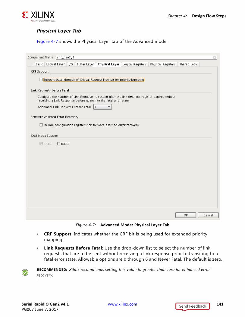
Serial RapidIO Gen2 v4.1 www.xilinx.com 141PG007 June 7, 2017
Chapter 4: Design Flow Steps
Physical Layer Tab
Figure 4-7 shows the Physical Layer tab of the Advanced mode.
• CRF Support: Indicates whether the CRF bit is being used for extended priority mapping.
• Link Requests Before Fatal: Use the drop-down list to select the number of link requests that are to be sent without receiving a link response prior to transiting to a fatal error state. Allowable options are 0 through 6 and Never Fatal. The default is zero.
RECOMMENDED: Xilinx recommends setting this value to greater than zero for enhanced error recovery.
X-Ref Target - Figure 4-7
Figure 4-7: Advanced Mode: Physical Layer Tab
Send Feedback

Serial RapidIO Gen2 v4.1 www.xilinx.com 142PG007 June 7, 2017
Chapter 4: Design Flow Steps
• Software Assisted Error Recovery: The RapidIO Specification defines three Command and Status Registers specifically for software-assisted error recovery. Specifically the Port n Link Maintenance Request CSR in Chapter 2, Port n Link Maintenance Response CSR in Chapter 2, and the Port n Local ackID CSR in Chapter 2.
• IDLE Mode Support: The supported IDLE modes vary based on the transfer frequency chosen on the Component/System Generation Page. IDLE1 operation is only supported for line rates of 5.0 Gbaud or less per lane. Use of the IDLE1 sequence means that the short control symbol format is used. The IDLE2 sequence was designed for links operating above 5.0 Gbaud per lane. Rates of 6.25 Gbaud only operate with IDLE2 sequence. The IDLE2 sequence provides additional functionality (link width and lane polarity information, plus randomized data for equalizer training for improved data recovery). If both the IDLE1 and IDLE2 sequences are enabled (only possible for 5.0 Gbaud or less), the core trains with the link partner as described in the RapidIO Specification to select an IDLE sequence.
Logical Registers Tab
Figure 4-8 shows the Logical Registers tab of the Advanced mode.
• Device Identity CAR: The Device Identity CAR stores information about a RapidIO device. This register holds Xilinx-assigned fields and is not modifiable.
X-Ref Target - Figure 4-8
Figure 4-8: Advanced Mode: Logical Registers Tab
Send Feedback
Serial RapidIO Gen2 v4.1 www.xilinx.com 143PG007 June 7, 2017
Chapter 4: Design Flow Steps
• Assembly Identity CAR: The Assembly Identity CAR stores information about a RapidIO device subsystem creator. You can set the Assembly Identifier and Assembly Vendor Identifier fields of the register during core generation to uniquely identify the Endpoint. These values do not affect core functionality.
• Assembly Information CAR: The Assembly Information CAR stores information about a RapidIO device subsystem revision. This is set during core generation and does not affect core functionality.
• Processing Element Features CAR: Selects the major functionality provided by the processing element. Allowable options are:
° Bridge
° Memory
° Processor
° Bridge and Memory
Memory is the default setting. This field does not alter core functionality.
Send Feedback
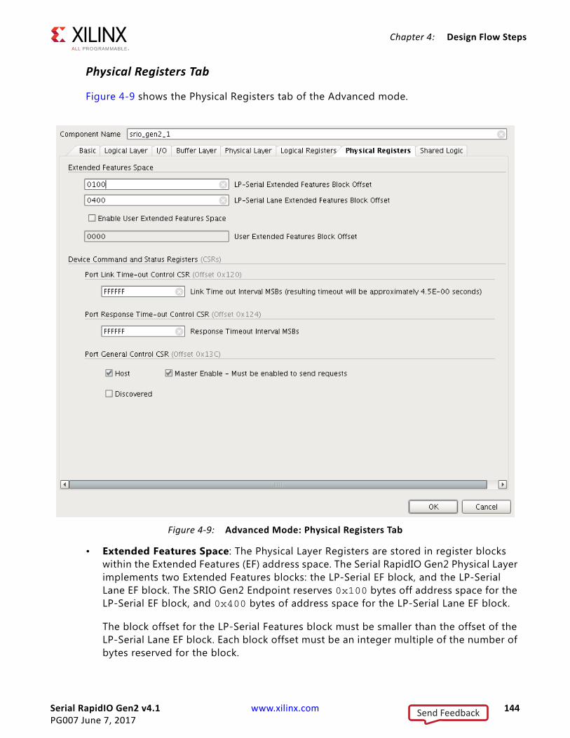
Serial RapidIO Gen2 v4.1 www.xilinx.com 144PG007 June 7, 2017
Chapter 4: Design Flow Steps
Physical Registers Tab
Figure 4-9 shows the Physical Registers tab of the Advanced mode.
• Extended Features Space: The Physical Layer Registers are stored in register blocks within the Extended Features (EF) address space. The Serial RapidIO Gen2 Physical Layer implements two Extended Features blocks: the LP-Serial EF block, and the LP-Serial Lane EF block. The SRIO Gen2 Endpoint reserves 0x100 bytes off address space for the LP-Serial EF block, and 0x400 bytes of address space for the LP-Serial Lane EF block.
The block offset for the LP-Serial Features block must be smaller than the offset of the LP-Serial Lane EF block. Each block offset must be an integer multiple of the number of bytes reserved for the block.
X-Ref Target - Figure 4-9
Figure 4-9: Advanced Mode: Physical Registers Tab
Send Feedback

Serial RapidIO Gen2 v4.1 www.xilinx.com 145PG007 June 7, 2017
Chapter 4: Design Flow Steps
You can implement one or more EF blocks within the Extended Features address space as well. The user application would have to create these registers somewhere and modify the Configuration Fabric reference design to accommodate the additional register block. If a User EF is being implemented, it should be enabled in the Vivado IDE, and the block offset of the first EF block should be entered. That offset must be greater than the LP-Serial Lane EF block offset plus the 0x400 byte size that was reserved for that block. The User EF block offset must be a multiple of 0x100 and within the Extended Features address space.
See Extended Features Space in Chapter 2 for more information.
• Device Command and Status Registers (CSRs)
° Port Link Time-out Control CSR (Offset 0x120): Timeout value the PHY uses when determining a link control symbol, such as Packet Accepted or Link Response, has been lost. When this counter expires, link protocol as defined in the RapidIO Serial PHY specification is followed. The max timeout scales linearly with the value in this CSR. A max timeout value of FF_FFFFh corresponds to a timeout length of approximately 4.5 seconds, but the max value is only accurate to within ± 33%.
° Port Response Time-out Control CSR: Timeout value to be used by an end-point to determine a lost packet. A max timeout value of FF_FFFFh should correspond to a timeout length of between 3 and 6 seconds. Implementation of the response timeout is left to you.
° Port General Control CSR: The Host bit indicates that the device is a host device. If this bit is not set, the device is an agent or a slave. This bit does not affect core functionality. The Master Enable bit controls whether or not a device is allowed to issue requests to the system. If the Master Enable bit is not set, the device might only respond to requests.
Note: If Master Enable is unchecked, the device cannot initiate requests until the bit is written with a 1.
The Discovered bit indicates that the device has been located by the processing element responsible for system configuration. This bit does not affect endpoint operation.
Send Feedback
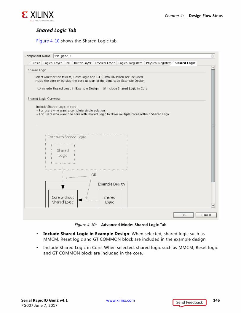
Serial RapidIO Gen2 v4.1 www.xilinx.com 146PG007 June 7, 2017
Chapter 4: Design Flow Steps
Shared Logic Tab
Figure 4-10 shows the Shared Logic tab.
• Include Shared Logic in Example Design: When selected, shared logic such as MMCM, Reset logic and GT COMMON block are included in the example design.
• Include Shared Logic in Core: When selected, shared logic such as MMCM, Reset logic and GT COMMON block are included in the core.
X-Ref Target - Figure 4-10
Figure 4-10: Advanced Mode: Shared Logic Tab
Send Feedback
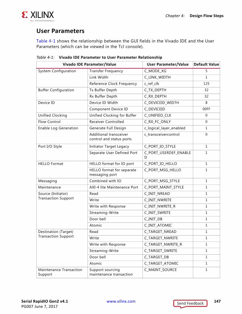
Serial RapidIO Gen2 v4.1 www.xilinx.com 147PG007 June 7, 2017
Chapter 4: Design Flow Steps
User ParametersTable 4-1 shows the relationship between the GUI fields in the Vivado IDE and the User Parameters (which can be viewed in the Tcl console).
Table 4-1: Vivado IDE Parameter to User Parameter RelationshipVivado IDE Parameter/Value User Parameter/Value Default Value
System Configuration Transfer Frequency C_MODE_XG 5
Link Width C_LINK_WIDTH 1
Reference Clock Frequency c_ref_clk 125
Buffer Configuration Tx Buffer Depth C_TX_DEPTH 32
Rx Buffer Depth C_RX_DEPTH 32
Device ID Device ID Width C_DEVICEID_WIDTH 8
Component Device ID C_DEVICEID 00FF
Unified Clocking Unified Clocking for Buffer C_UNIFIED_CLK 0
Flow Control Receiver Controlled C_RX_FC_ONLY 0
Enable Log Generation Generate Full Design c_logical_layer_enabled 1
Additional transceiver control and status ports
c_transceivercontrol 0
Port I/O Style Initiator Target Legacy C_PORT_IO_STYLE 1
Separate User Defined Port C_PORT_USERDEF_ENABLED
1
HELLO Format HELLO format for IO port C_PORT_IO_HELLO 1
HELLO format for separate messaging port
C_PORT_MSG_HELLO 1
Messaging Combined with IO C_PORT_MSG_STYLE 1
Maintenance AXI-4 lite Maintenance Port C_PORT_MAINT_STYLE 1
Source (Initiator) Transaction Support
Read C_INIT_NREAD 1
Write C_INIT_NWRITE 1
Write with Response C_INIT_NWRITE_R 1
Streaming-Write C_INIT_SWRITE 1
Door bell C_INIT_DB 1
Atomic C_INIT_ATOMIC 1
Destination (Target) Transaction Support
Read C_TARGET_NREAD 1
Write C_TARGET_NWRITE 1
Write with Response C_TARGET_NWRITE_R 1
Streaming-Write C_TARGET_SWRITE 1
Door bell C_TARGET_DB 1
Atomic C_TARGET_ATOMIC 1
Maintenance Transaction Support
Support sourcing maintenance transaction
C_MAINT_SOURCE 1
Send Feedback
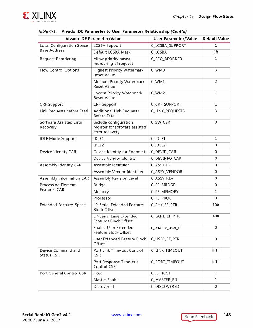
Serial RapidIO Gen2 v4.1 www.xilinx.com 148PG007 June 7, 2017
Chapter 4: Design Flow Steps
Local Configuration Space Base Address
LCSBA Support C_LCSBA_SUPPORT 1
Default LCSBA Mask C_LCSBA 3ff
Request Reordering Allow priority based reordering of request
C_REQ_REORDER 1
Flow Control Options Highest Priority Watermark Reset Value
C_WM0 3
Medium Priority Watermark Reset Value
C_WM1 2
Lowest Priority Watermark Reset Value
C_WM2 1
CRF Support CRF Support C_CRF_SUPPORT 1
Link Requests before Fatal Additional Link Requests Before Fatal
C_LINK_REQUESTS 3
Software Assisted Error Recovery
Include configuration register for software assisted error recovery
C_SW_CSR 0
IDLE Mode Support IDLE1 C_IDLE1 1
IDLE2 C_IDLE2 0
Device Identity CAR Device Identity for Endpoint C_DEVID_CAR 0
Device Vendor Identity C_DEVINFO_CAR 0
Assembly Identity CAR Assembly Identifier C_ASSY_ID 0
Assembly Vendor Identifier C_ASSY_VENDOR 0
Assembly Information CAR Assembly Revision Level C_ASSY_REV 0
Processing Element Features CAR
Bridge C_PE_BRIDGE 0
Memory C_PE_MEMORY 1
Processor C_PE_PROC 0
Extended Features Space LP-Serial Extended Features Block Offset
C_PHY_EF_PTR 100
LP-Serial Lane Extended Features Block Offset
C_LANE_EF_PTR 400
Enable User Extended Feature Block Offset
c_enable_user_ef 0
User Extended Feature Block Offset
C_USER_EF_PTR 0
Device Command and Status CSR
Port Link Time-out Control CSR
C_LINK_TIMEOUT ffffff
Port Response Time-out Control CSR
C_PORT_TIMEOUT ffffff
Port General Control CSR Host C_IS_HOST 1
Master Enable C_MASTER_EN 1
Discovered C_DISCOVERED 0
Table 4-1: Vivado IDE Parameter to User Parameter Relationship (Cont’d)
Vivado IDE Parameter/Value User Parameter/Value Default Value
Send Feedback
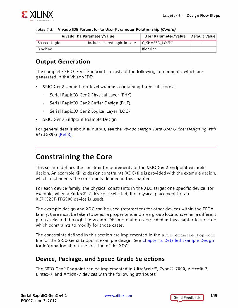
Serial RapidIO Gen2 v4.1 www.xilinx.com 149PG007 June 7, 2017
Chapter 4: Design Flow Steps
Output GenerationThe complete SRIO Gen2 Endpoint consists of the following components, which are generated in the Vivado IDE:
• SRIO Gen2 Unified top-level wrapper, containing three sub-cores:
° Serial RapidIO Gen2 Physical Layer (PHY)
° Serial RapidIO Gen2 Buffer Design (BUF)
° Serial RapidIO Gen2 Logical Layer (LOG)
• SRIO Gen2 Endpoint Example Design
For general details about IP output, see the Vivado Design Suite User Guide: Designing with IP (UG896) [Ref 3].
Constraining the CoreThis section defines the constraint requirements of the SRIO Gen2 Endpoint example design. An example Xilinx design constraints (XDC) file is provided with the example design, which implements the constraints defined in this chapter.
For each device family, the physical constraints in the XDC target one specific device (for example, when a Kintex®-7 device is selected, the physical placement for an XC7K325T-FFG900 device is used).
The example design and XDC can be used (retargeted) for other devices within the FPGA family. Care must be taken to select a proper pins and area group locations when a different part is selected through the Vivado IDE. Information is provided in this chapter to indicate which constraints to modify for those cases.
The constraints defined in this section are implemented in the srio_example_top.xdc file for the SRIO Gen2 Endpoint example design. See Chapter 5, Detailed Example Design for information about the location of the XDC.
Device, Package, and Speed Grade SelectionsThe SRIO Gen2 Endpoint can be implemented in UltraScale™, Zynq®-7000, Virtex®-7, Kintex-7, and Artix®-7 devices with the following attributes:
Shared Logic Include shared logic in core C_SHARED_LOGIC 1
Blocking Blocking
Table 4-1: Vivado IDE Parameter to User Parameter Relationship (Cont’d)
Vivado IDE Parameter/Value User Parameter/Value Default Value
Send Feedback

Serial RapidIO Gen2 v4.1 www.xilinx.com 150PG007 June 7, 2017
Chapter 4: Design Flow Steps
• Large enough to accommodate the SRIO Gen2 Endpoint design
• Fast enough speed grade to meet the requirements listed in the Serial RapidIO Gen2 Product Specification
• Transceivers capable of running at the core configured line rate
Clock FrequenciesThe XDC applies the clock constraint on the input reference clock, which gets pushed through the clocking components and applied to each distinct clock domain. If a second source clock is used, a similar constraint must be applied to that clock as well.
The clock constraint specifies the frequency and duty-cycle of the source clock signal in the design. The following is the applied constraint for a 125 MHz reference frequency.
create_clock -period 8 -name sys_clkp -waveform {0 4} [get_ports sys_clkp]
For other configurations, the clock period is adjusted accordingly.
Clock ManagementAdvanced timing closure techniques might be needed to meet timing for 5.0 Gbaud or greater operation. For example, an area group might facilitate placement so that routing delays are minimized. Generally, the area group should be large enough to contain enough logic resources for the core, but small enough to have an impact on timing. Optimal size varies with core configuration.
Example syntax:
create_pblock pblock_phyadd_cells_to_pblock [get_pblocks pblock_phy] [get_cells -quiet -hierarchical *ollm_tx_top_inst]add_cells_to_pblock [get_pblocks pblock_phy] [get_cells -quiet -hierarchical *ollm_rx_top_inst]resize_pblock [get_pblocks pblock_phy] -add {SLICE_X122Y300:SLICE_X137Y349}
Currently, no configurations use area groups. Any area groups in the XDC are currently commented out. For more information on area group constraints, see Xilinx Timing Constraints User Guide (UG612) [Ref 2].
Additional steps that might be necessary to meet timing in certain devices:
• Location constraints for block RAMs
• Changing software options
• Reconfiguring the core with fewer features
Send Feedback

Serial RapidIO Gen2 v4.1 www.xilinx.com 151PG007 June 7, 2017
Chapter 4: Design Flow Steps
Clock PlacementNo clock placement constraints are required.
BankingNo banking constraints are required.
Transceiver PlacementThe provided XDC uses placement constraints to specify the serial transceivers that is used when the core is implemented. These can be moved around, but all lanes within a given core should be placed in adjacent transceivers for best timing results. The following constraints are provided by default with 4x Kintex-7 FPGA cores. If an UltraScale device is selected, transceiver locations are automatically populated in the XDC file. You do not need to edit any information in the XDC file for GT locations.
set_property LOC E3 [get_ports srio_rxn0]set_property LOC E4 [get_ports srio_rxp0]set_property LOC D1 [get_ports srio_txn0]set_property LOC D2 [get_ports srio_txp0]set_property LOC D5 [get_ports srio_rxn1]set_property LOC D6 [get_ports srio_rxp1]set_property LOC C3 [get_ports srio_txn1]set_property LOC C4 [get_ports srio_txp1]set_property LOC B5 [get_ports srio_rxn2]set_property LOC B6 [get_ports srio_rxp2]set_property LOC B1 [get_ports srio_txn2]set_property LOC B2 [get_ports srio_txp2]set_property LOC A7 [get_ports srio_rxn3]set_property LOC A8 [get_ports srio_rxp3]set_property LOC A3 [get_ports srio_txn3]set_property LOC A4 [get_ports srio_txp3]
I/O Standard and PlacementThe XDC constrains the I/O placement and I/O standard. These can be moved to any free location that also meets I/O placement and banking rules. The following is an example of the constraints applied to the Kintex-7 FPGA cores.
set_property LOC C8 [get_ports sys_clkp]set_property LOC C7 [get_ports sys_clkn]set_property LOC K18 [get_ports sys_rst]set_property LOC C19 [get_ports sim_train_en]
set_property IOSTANDARD LVCMOS18 [get_ports sys_rst]set_property IOSTANDARD LVCMOS18 [get_ports sim_train_en]
Send Feedback
Serial RapidIO Gen2 v4.1 www.xilinx.com 152PG007 June 7, 2017
Chapter 4: Design Flow Steps
SimulationFor comprehensive information about Vivado Design Suite simulation components, as well as information about using supported third party tools, see the Vivado Design Suite User Guide: Logic Simulation (UG900) [Ref 7].
For information about simulating the example design, see Simulating the Example Design in Chapter 5.
IMPORTANT: For cores targeting 7 series or Zynq-7000 devices, UNIFAST libraries are not supported. Xilinx IP is tested and qualified with UNISIM libraries only.
Synthesis and ImplementationFor details about synthesis and implementation, see “Synthesizing IP” and “Implementing IP” in the Vivado Design Suite User Guide: Designing with IP (UG896) [Ref 3].
Send Feedback
Serial RapidIO Gen2 v4.1 www.xilinx.com 153PG007 June 7, 2017
Chapter 5
Detailed Example DesignThis chapter introduces the SRIO Gen2 Endpoint reference design that is included with the SRIO Gen2 Endpoint. The reference design demonstrates how to generate the SRIO Gen2 Endpoint, including the LOG, BUF, and PHY provided through the SRIO Gen2 Endpoint top-level wrapper. In addition, the reference design illustrates using the default options in the SRIO Gen2 Endpoint example design.
OverviewThe SRIO Gen2 Endpoint example design connects two instances of the core together. Each core instance can be configured to send supported packet types, check for receive packet mismatches, and report in the simulation transcript with details about the link traffic. Both the simulation host and the primary core being tested use the SRIO Gen2 Endpoint reference design (consisting of a LOG, BUF, and PHY provided through the SRIO Gen2 Endpoint top-level wrapper) and the Configuration Fabric reference design.
Generating the CoreBefore using the SRIO Gen2 Endpoint, the PHY and LOG must be generated through the Vivado® Design Suite. To do so, generate a core in the Vivado Integrated Design Environment (IDE) as described in “Working with IP” and “Customizing IP for the Design” in the Vivado Design Suite User Guide: Designing with IP (UG896) [Ref 3], and in “Working with the Vivado IDE” in the Vivado Design Suite User Guide: Getting Started (UG910) [Ref 5].
IMPORTANT: Use the default values when generating the Serial RapidIO Gen2 core.
The cores and supporting files, such as the SRIO Gen2 Endpoint example design, are generated in the <project_dir>/<project_dir>.srcs/sources_1/ip/<component_name> directory.
Send Feedback
Serial RapidIO Gen2 v4.1 www.xilinx.com 154PG007 June 7, 2017
Chapter 5: Detailed Example Design
Directory and File ContentsThe complete SRIO Gen2 Endpoint consists of the following components:
• SRIO Gen2 Unified top-level wrapper containing:
° Serial RapidIO Gen2 Physical Layer (PHY)
° Serial RapidIO Gen2 Buffer Design (BUF)
° Serial RapidIO Gen2 Logical Layer (LOG)
• SRIO Gen2 Endpoint Example Design
The SRIO Gen2 Endpoint includes a configuration fabric reference design, example clock and reset modules, and an example user design.
The SRIO Gen2 Endpoint also includes synthesis and implementation scripts, simulation scripts, a demonstration test bench, and supporting simulation files for the example design. For the implementation and simulation scripts to work, all three sub-cores (PHY, BUF, and LOG) must be generated in the same project directory.
SRIO Gen2 Endpoint Directory StructureAs illustrated in the following directory structure:
• The Vivado Design Suite project is <project_dir>.
• The component name for the SRIO Gen2 Endpoint top-level wrapper is <srio_component_name>.
<project_dir>/<project_dir>.srcs/sources_1/ip/<component_name>This directory contains the directories for the SRIO Gen2 Endpoint example design and the implementation and simulation examples.
Table 5-1: Project Directory
Name Description
<project_dir>/<project_dir>.srcs/sources_1/ip/<component_name>
<component_name>.veo The HDL template for the SRIO Gen2 Endpoint top-level wrapper.
<component_name>.xml Core file.
<component_name>.xci Core configuration options file.
Send Feedback
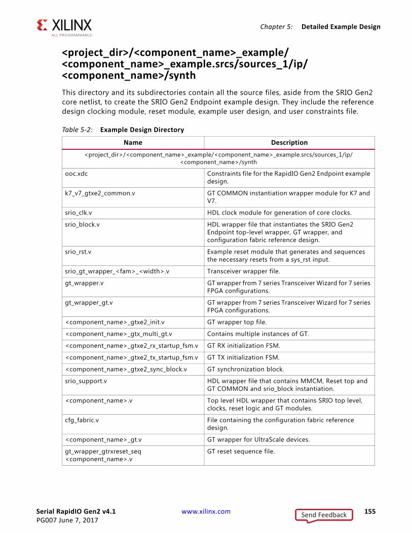
Serial RapidIO Gen2 v4.1 www.xilinx.com 155PG007 June 7, 2017
Chapter 5: Detailed Example Design
<project_dir>/<component_name>_example/<component_name>_example.srcs/sources_1/ip/<component_name>/synthThis directory and its subdirectories contain all the source files, aside from the SRIO Gen2 core netlist, to create the SRIO Gen2 Endpoint example design. They include the reference design clocking module, reset module, example user design, and user constraints file.
Table 5-2: Example Design Directory
Name Description
<project_dir>/<component_name>_example/<component_name>_example.srcs/sources_1/ip/<component_name>/synth
ooc.xdc Constraints file for the RapidIO Gen2 Endpoint example design.
k7_v7_gtxe2_common.v GT COMMON instantiation wrapper module for K7 and V7.
srio_clk.v HDL clock module for generation of core clocks.
srio_block.v HDL wrapper file that instantiates the SRIO Gen2 Endpoint top-level wrapper, GT wrapper, and configuration fabric reference design.
srio_rst.v Example reset module that generates and sequences the necessary resets from a sys_rst input.
srio_gt_wrapper_<fam>_<width>.v Transceiver wrapper file.
gt_wrapper.v GT wrapper from 7 series Transceiver Wizard for 7 series FPGA configurations.
gt_wrapper_gt.v GT wrapper from 7 series Transceiver Wizard for 7 series FPGA configurations.
<component_name>_gtxe2_init.v GT wrapper top file.
<component_name>_gtx_multi_gt.v Contains multiple instances of GT.
<component_name>_gtxe2_rx_startup_fsm.v GT RX initialization FSM.
<component_name>_gtxe2_tx_startup_fsm.v GT TX initialization FSM.
<component_name>_gtxe2_sync_block.v GT synchronization block.
srio_support.v HDL wrapper file that contains MMCM, Reset top and GT COMMON and srio_block instantiation.
<component_name>.v Top level HDL wrapper that contains SRIO top level, clocks, reset logic and GT modules.
cfg_fabric.v File containing the configuration fabric reference design.
<component_name>_gt.v GT wrapper for UltraScale devices.
gt_wrapper_gtrxreset_seq<component_name>.v
GT reset sequence file.
Send Feedback
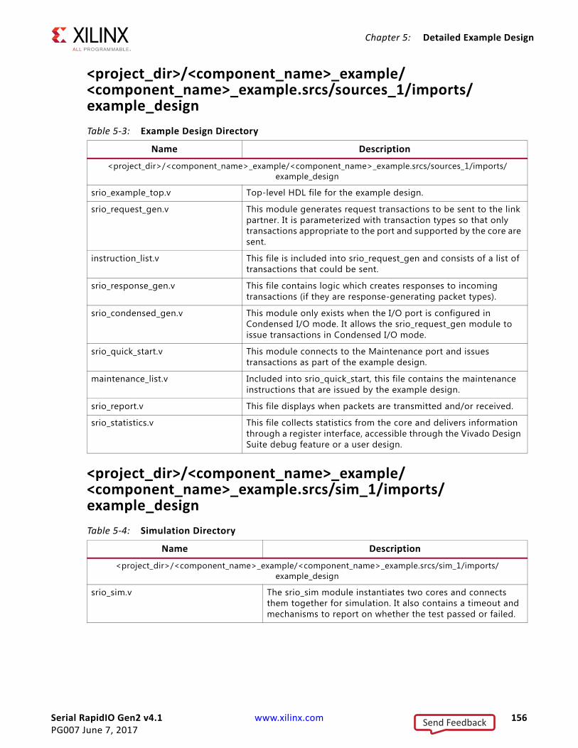
Serial RapidIO Gen2 v4.1 www.xilinx.com 156PG007 June 7, 2017
Chapter 5: Detailed Example Design
<project_dir>/<component_name>_example/<component_name>_example.srcs/sources_1/imports/example_design
<project_dir>/<component_name>_example/<component_name>_example.srcs/sim_1/imports/example_design
Table 5-3: Example Design Directory
Name Description
<project_dir>/<component_name>_example/<component_name>_example.srcs/sources_1/imports/example_design
srio_example_top.v Top-level HDL file for the example design.
srio_request_gen.v This module generates request transactions to be sent to the link partner. It is parameterized with transaction types so that only transactions appropriate to the port and supported by the core are sent.
instruction_list.v This file is included into srio_request_gen and consists of a list of transactions that could be sent.
srio_response_gen.v This file contains logic which creates responses to incoming transactions (if they are response-generating packet types).
srio_condensed_gen.v This module only exists when the I/O port is configured in Condensed I/O mode. It allows the srio_request_gen module to issue transactions in Condensed I/O mode.
srio_quick_start.v This module connects to the Maintenance port and issues transactions as part of the example design.
maintenance_list.v Included into srio_quick_start, this file contains the maintenance instructions that are issued by the example design.
srio_report.v This file displays when packets are transmitted and/or received.
srio_statistics.v This file collects statistics from the core and delivers information through a register interface, accessible through the Vivado Design Suite debug feature or a user design.
Table 5-4: Simulation Directory
Name Description
<project_dir>/<component_name>_example/<component_name>_example.srcs/sim_1/imports/example_design
srio_sim.v The srio_sim module instantiates two cores and connects them together for simulation. It also contains a timeout and mechanisms to report on whether the test passed or failed.
Send Feedback

Serial RapidIO Gen2 v4.1 www.xilinx.com 157PG007 June 7, 2017
Chapter 5: Detailed Example Design
Example DesignThe srio_example_top module instantiates all components of the core and example design that are needed to implement the design in hardware, as shown in Figure 5-1. This includes the clock and reset modules, the configuration fabric, and stimulus generators to create transactions.
Send Feedback
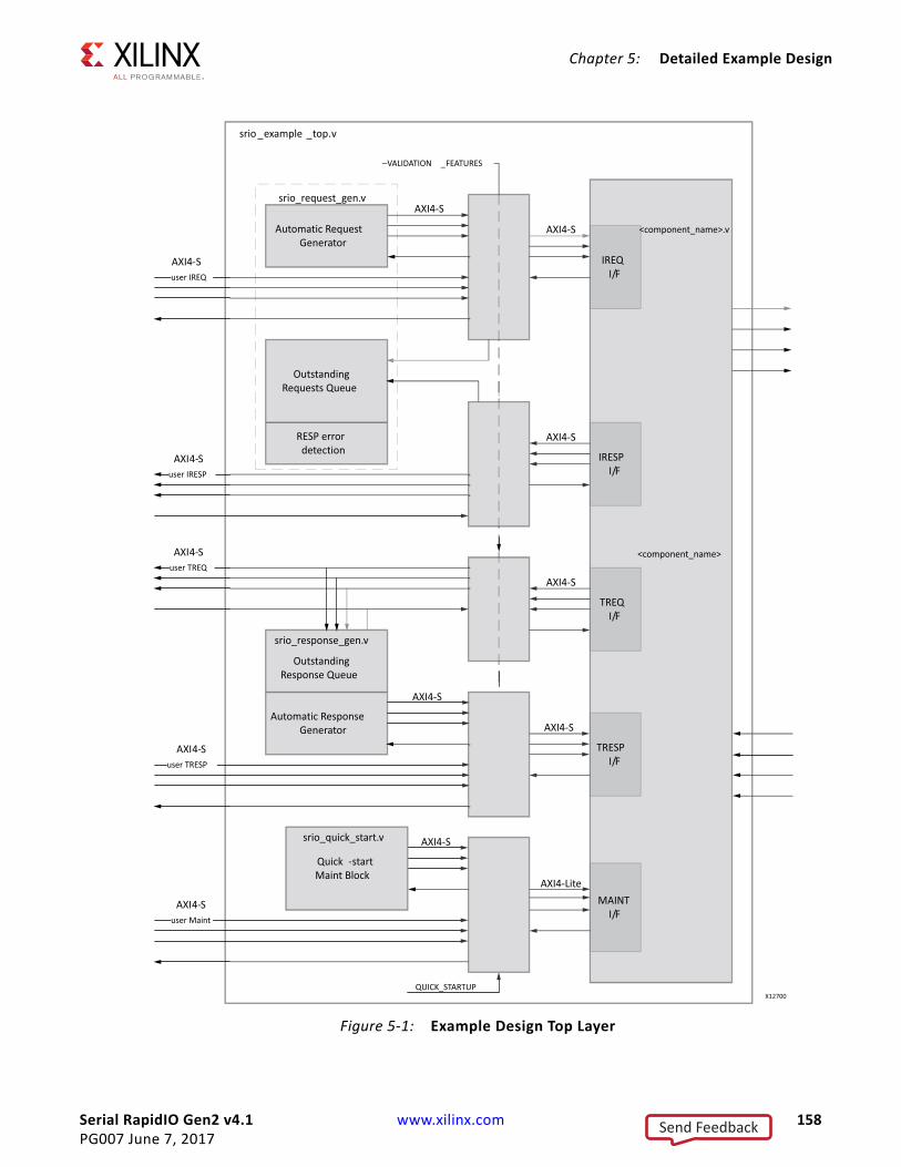
Serial RapidIO Gen2 v4.1 www.xilinx.com 158PG007 June 7, 2017
Chapter 5: Detailed Example Design
X-Ref Target - Figure 5-1
Figure 5-1: Example Design Top Layer
<component_name>
Outstanding Requests Queue
Automatic Request Generator
AXI4-S
AXI4-S
VALIDATION _FEATURES
user IREQ
AXI4-S
AXI4-S
user IRESP
AXI4-S
RESP error detection
AXI4-S
Outstanding Response Queue
Automatic Response Generator
user TREQ
AXI4-S
AXI4-Lite
AXI4-S
user TRESP
AXI4-S
Quick -startMaint Block
QUICK_STARTUP
AXI4-S
AXI4-S
AXI4-Suser Maint
IREQI/F
IRESPI/F
TREQI/F
TRESPI/F
MAINTI/F
srio _example _top.v
<component_name>.v
srio_quick_start.v
srio_response_gen.v
srio_request_gen.v
X12700
Send Feedback
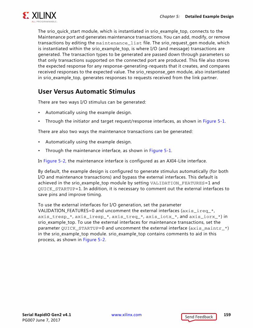
Serial RapidIO Gen2 v4.1 www.xilinx.com 159PG007 June 7, 2017
Chapter 5: Detailed Example Design
The srio_quick_start module, which is instantiated in srio_example_top, connects to the Maintenance port and generates maintenance transactions. You can add, modify, or remove transactions by editing the maintenance_list file. The srio_request_gen module, which is instantiated within the srio_example_top, is where I/O (and message) transactions are generated. The transaction types to be generated are passed down through parameters so that only transactions supported on the connected port are produced. This file also stores the expected response for any response-generating-requests that it creates, and compares received responses to the expected value. The srio_response_gen module, also instantiated in srio_example_top, generates responses to requests received from the link partner.
User Versus Automatic StimulusThere are two ways I/O stimulus can be generated:
• Automatically using the example design.
• Through the initiator and target request/response interfaces, as shown in Figure 5-1.
There are also two ways the maintenance transactions can be generated:
• Automatically using the example design.
• Through the maintenance interface, as shown in Figure 5-1.
In Figure 5-2, the maintenance interface is configured as an AXI4-Lite interface.
By default, the example design is configured to generate stimulus automatically (for both I/O and maintenance transactions) and bypass the external interfaces. This default is achieved in the srio_example_top module by setting VALIDATION_FEATURES=1 and QUICK_STARTUP=1. In addition, it is necessary to comment out the external interfaces to save pins and improve timing.
To use the external interfaces for I/O generation, set the parameter VALIDATION_FEATURES=0 and uncomment the external interfaces (axis_ireq_*, axis_tresp_*, axis_iresp_*, axis_treq_*, axis_iotx_*, and axis_iorx_*) in srio_example_top. To use the external interfaces for maintenance transactions, set the parameter QUICK_STARTUP=0 and uncomment the external interface (axis_maintr_*) in the srio_example_top module. srio_example_top contains comments to aid in this process, as shown in Figure 5-2.
Send Feedback
Serial RapidIO Gen2 v4.1 www.xilinx.com 160PG007 June 7, 2017
Chapter 5: Detailed Example Design
X-Ref Target - Figure 5-2
Figure 5-2: RTL Layer Block Diagram
AXI4-S
AXI4-Lite
IREQI/F
IRESPI/F
TREQI/F
TRESPI/F
MAINTI/F
<component_name>.v
<component_name>_block
Clock Module
srio_clk.v
Configuration Fabric
cfg_fabric.v
LOG Layer PHY Layer PHY Layer
GT Wrapper
srio_gt_wrapper_<family>_<width>.v
Reset Module
srio_rst.v
srio_gen2_unifiedtop
X12701
AXI4-S
AXI4-S
AXI4-S
Send Feedback
Serial RapidIO Gen2 v4.1 www.xilinx.com 161PG007 June 7, 2017
Chapter 5: Detailed Example Design
Automatic Stimulus GenerationBy default, the example design generates stimulus automatically for both the I/O and maintenance transactions. The maintenance transactions are generated in the srio_quick_start module, and the transactions are specifically listed out in the maintenance_list.vh file.
These maintenance transactions are examples of a typical configuration of the core when coming out of reset. Transactions can also be added, modified, or removed in maintenance_list module. The srio_quick_start.vh is intended to be implemented in designs for managing common maintenance transactions if no processor is needed. This method is only good for setting up the core when coming out of reset.
The I/O transactions are generated in the srio_request_gen and srio_response_gen modules. The srio_request_gen generates the initiator request I/O transactions as specified in instruction_list.vh file.
Transactions can be added, modified, or removed in instruction_list.vh. The list contains random transactions, but is run in the same order each time. Only transactions supported by the connected port are produced. Figure 5-1 shows an example of a core configured with Initiator/Target Legacy ports. The srio_request_gen also keeps track of any expected responses for response-generating-requests, and compares the received response to the expected value. This comparison function is only available when using the automatic stimulus generation.
The srio_response_gen generates the target response I/O transactions in response to requests received from the link partner. The data payload of write requests that fall within the scratch space of x0012_xxxx are stored in a local memory. All other write requests that do not require a response are dropped, and the srio_response_gen does not respond to SWRITE transaction types. Read requests that fall in the scratch space of x0012_xxxx get a response with data from that actual address. For instructions with an address offset outside of the scratch space, the response generator automatically fills the I/O transaction data with an increasing pattern. The responses are generated in the order that the requests are received; so no out-of-order transactions are generated. In all cases, response priorities are equal to the request priority plus 1.
• Each instance of the srio_request_gen requires one block RAM.
• Each instance of srio_response_gen requires two block RAM resources.
Configuration FabricThe Configuration Space is distributed across all the blocks of the SRIO Gen2 Endpoint. The Configuration Fabric reference design, located in the cfg_fabric module of the example design, manages the accesses to the configuration spaces of each of the blocks. This makes them appear unified to the user or processor element. The configuration modules in each of the blocks are slaves on the configuration bus (an AXI-Lite interface), and the
Send Feedback
Serial RapidIO Gen2 v4.1 www.xilinx.com 162PG007 June 7, 2017
Chapter 5: Detailed Example Design
Configuration Fabric module is the bus master. Reads and writes derived from Maintenance transactions that were issued either locally or from the link partner are presented to the Configuration Fabric through the Configuration Master port in the LOG block. The Configuration Fabric routes the reads and writes to the appropriate block, but does not route any transactions if the address is outside the valid range for the respective configuration registers. Writes to illegal space are dropped, and reads from illegal space are returned as zeros. For more details, see Accessing the Configuration Space in Chapter 3.
Clock ModuleThe clock module in the example design is identical to the clock module delivered with the core, as described in Clocking in Chapter 3. The srio_clk module consists of one MMCM_ADV, one IBUFDS, and either three or four BUFGs depending on the selected family. In 2x or 4x mode, one of the BUFGs is converted to a BUFGMUX. The srio_clk module generates the appropriate reference frequencies and user clocks, depending on the configuration.
Reset ModuleThe srio_rst module, as shown in Figure 5-2, takes in one asynchronous reset, and outputs a pulse-extended synchronized reset for each clock domain. The srio_rst module also contains a state machine to cause a forced re-initialization when called by the user design. This module also resets the link when instructed to do so by the link partner.
Implementing the Example DesignAfter Generating the Core, implement the example design as described in “Implementing IP” in the Vivado Design Suite User Guide: Designing with IP (UG896) [Ref 3].
Simulating the Example DesignUsing the SRIO Gen2 Endpoint example design (delivered as part of the Serial SRIO Gen2 Endpoint), you can quickly simulate and observe the behavior of the SRIO Gen2 Endpoint.
Setting up the SimulationThe Xilinx simulation libraries must be mapped into the simulator. For information about setting up the simulator environment, see the Vivado Design Suite User Guide: Logic Simulation (UG900) [Ref 7].
Send Feedback

Serial RapidIO Gen2 v4.1 www.xilinx.com 163PG007 June 7, 2017
Chapter 5: Detailed Example Design
Simulations including the serial transceivers require a Verilog LRM-IEEE 1364-2005 encryption-compliant simulator.
To switch simulators, click Simulation Settings in the Flow Navigator (left pane). In the Simulation options list, change Target Simulator.
Functional SimulationThis section contains instructions for running a functional simulation of the SRIO Gen2 Endpoint using Verilog.
IMPORTANT: The example design supports functional (behavioral) and post-synthesis simulations.
• To run a functional simulation, click Run Simulation in the Flow Navigator (left pane) and then click Run Behavioral Simulation.
• To run a post-synthesis simulation, click Run Simulation in the Flow Navigator (left pane), and then click Run Post-Synthesis Functional Simulation.
Passing TransactionsBy default, the example design simulation only confirms that the core has achieved Port and Link Initialization. However, the test bench is also designed to stimulate the core by issuing and checking packet transfers. This feature might be enabled for behavioral simulation only.
To enable full packet transfer and self-checking:
1. Open the top-level simulation file, srio_sim.v, in the example design directory.
2. Find the two instantiations of the core. Enable the extended simulation features by uncommenting the parameters being passed in from the top level:
srio_example_top #(// NOTE: uncomment these lines to simulate packet transfer// .SIM_ONLY (0), // mirror object handles reporting// .SIM_TRAIN (1),// .VALIDATION_FEATURES (1),// .QUICK_STARTUP (1),// .USE_CHIPSCOPE (0),// .STATISTICS_GATHERING (1) ) srio_example_top_primary
srio_example_top #(// NOTE: uncomment these lines to simulate packet transfer// .SIM_ONLY (0), // mirror object handles reporting// .SIM_TRAIN (1),// .VALIDATION_FEATURES (1),// .QUICK_STARTUP (1),// .USE_CHIPSCOPE (0),// .STATISTICS_GATHERING (1) ) srio_example_top_mirror
Send Feedback
Serial RapidIO Gen2 v4.1 www.xilinx.com 164PG007 June 7, 2017
Chapter 5: Detailed Example Design
3. At the bottom, find the condition for success. Change the condition from Link and Port Initialized to Exercise Done:
// NOTE: Use this condition when simulating packet transfer// if (exercise_done_primary) begin if (link_initialized && port_initialized) begin
Self Checking SimulationThe simulation script compiles the SRIO Gen2 Endpoint functional simulation model, the SRIO Gen2 Endpoint example design, and supporting simulation files. It then runs the simulation and checks to ensure that it completed successfully. The simulation uses self-checking in the srio_request_gen module, as previously described. If any response does not match the expected type or ID, the test bench reports a mismatch:
************************************************************************************* ERROR: TEST FAILED ************************************* Packet Miscompare or Packet Corruption ******************************************************************************
If a response never returns, the simulation eventually times out:
################################################################################### ERROR: TEST FAILED !!!!! ######################################### Testbench Timed Out! ################################################ (<timestamp>) ##########################################################################################
A simulation success is indicated by this text:
********************************************************************************* Test Completed Successfully ********************************* All Packets Checked and Accounted For ******************************************************************************
To observe more details of the operation of the core, inspect the simulation transcript and the waveform.
Send Feedback
Serial RapidIO Gen2 v4.1 www.xilinx.com 165PG007 June 7, 2017
Chapter 6
Test BenchThis chapter contains information about the test bench provided in the Vivado® Design Suite.
Demonstration Test BenchThe srio_sim module, as shown in Figure 6-1, connects two instances of the example design (at the srio_example_top level) together. It generates the system clock and reset for simulation purposes, and monitors the simulation progress for status, including packet mis-compares, timeouts, and a tests complete flag. The two instances of the example design are:
• srio_example_top_primary, which represents the user core.
• srio_example_top_mirror, which acts as the link partner.
The srio_example_top_mirror is configured to report received and transmitted transactions into the simulation transcript. When a simulation completes, either due to an error or when all requests have been sent and responses received, the simulation stops and reports the simulation status in the transcript.
IMPORTANT: Because the test bench uses the mirror image of the original core configuration, you must select watermark levels that are not greater than the TX/RX buffer depth for simulation to work.
Send Feedback

Serial RapidIO Gen2 v4.1 www.xilinx.com 166PG007 June 7, 2017
Chapter 6: Test Bench
X-Ref Target - Figure 6-1
Figure 6-1: Example Design Test Bench Layer
<component_name> <component_name> mirror
X12195
srio_sim.v
srio_example_top.v srio_example_top.v
Send Feedback
Serial RapidIO Gen2 v4.1 www.xilinx.com 167PG007 June 7, 2017
Appendix A
Packet and Control Symbol Formats
ScopeThis appendix includes the block diagram for the RapidIO packet and control symbol format, which is based on the RapidIO Interconnect Specification rev. 2.2 [Ref 13].
Send Feedback
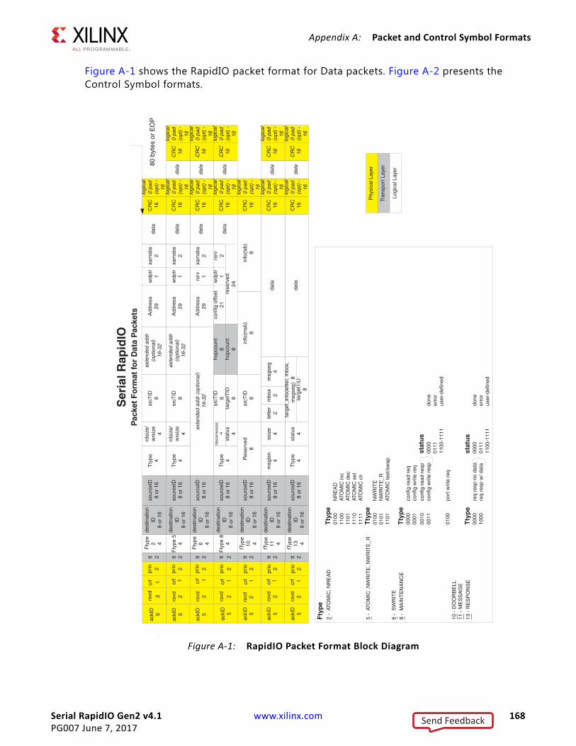
Serial RapidIO Gen2 v4.1 www.xilinx.com 168PG007 June 7, 2017
Appendix A: Packet and Control Symbol Formats
Figure A-1 shows the RapidIO packet format for Data packets. Figure A-2 presents the Control Symbol formats.
X-Ref Target - Figure A-1
Figure A-1: RapidIO Packet Format Block Diagram
Fty
pe 2 4
Tty
pe 4
rdsi
ze/
wrs
ize
4
srcT
ID8
exte
nded
add
r(o
ptio
nal)
16-3
2
Add
ress
29w
dptr
1xa
msb
s2
exte
nded
add
r (o
ptio
nal)
16-3
2A
ddre
ss29
rsrv 1
xam
sbs
2da
ta
Tty
pe 4
rdsi
ze/w
rsiz
e-4
srcT
ID8
conf
ig o
ffset
21w
dptr
1rs
rv 2da
tast
atus 4
targ
etT
ID8
rese
rved
24
Tty
pe 4st
atus 4
data
Res
erve
d8
srcT
ID8
info
(msb
)8
msg
len
4ss
ize
4da
ta
targ
etT
ID8
targ
et_i
nfo(
lette
r, m
box,
msg
seg)
8msg
seg
4le
tter
2m
box
2
prio 2 prio 2 prio 2 prio 2 prio 2 prio 2
tt 2 tt 2 tt 2 tt 2tt 2 tt 2
Fty
pe 6 4
Fty
pe 8
4
fTyp
e13 4
fTyp
e10 4
fTyp
e11 4
dest
inat
ion
ID8
or 1
6
dest
inat
ion
ID8
or 1
6
dest
inat
ion
ID8
or 1
6
dest
inat
ion
ID8
or 1
6
dest
inat
ion
ID8
or 1
6
dest
inat
ion
ID8
or 1
6
sour
ceID
8 or
16
sour
ceID
8 or
16
sour
ceID
8 or
16
sour
ceID
8 or
16
sour
ceID
8 or
16
sour
ceID
8 or
16
CR
C16 CR
C16 CR
C16 CR
C16 CR
C16 CR
C16
logi
cal
0 pa
d(o
pt)
-16
logi
cal
0 pa
d(o
pt)
-16
logi
cal
0 pa
d(o
pt)
-16
logi
cal
0 pa
d(o
pt)
-16
logi
cal
0 pa
d(o
pt)
-16
logi
cal
0 pa
d(o
pt)
-16
CR
C16 CR
C16 CR
C16 CR
C16
logi
cal
0 pa
d(o
pt)
-16
logi
cal
0 pa
d(o
pt)
-16
logi
cal
0 pa
d(o
pt)
-16
logi
cal
0 pa
d(o
pt)
-16
data
data
data
data
Pac
ket
Fo
rmat
for
Dat
a P
acke
ts
Phy
sica
l Lay
er
Tran
spor
t Lay
er
Logi
cal L
ayer
Tty
pe 4
rdsi
ze/
wrs
ize
4
srcT
ID8
exte
nded
add
r(o
ptio
nal)
16-3
2
Add
ress
29w
dptr
1xa
msb
s2
data
prio 2
tt 2F
type
54
dest
inat
ion
ID8
or 1
6
sour
ceID
8 or
16
CR
C16
logi
cal
0 pa
d(o
pt)
-16
CR
C16
logi
cal
0 pa
d(o
pt)
-16
data
data
Ser
ial R
apid
IO
80 b
ytes
or
EO
P
hopc
ount
8ho
pcou
nt8
info
(lsb)
8
ackI
D5
rsvd 2
ackI
D5
rsvd 2
ackI
D5
rsvd 2
ackI
D5
rsvd 2
ackI
D5
rsvd 2
ackI
D5
rsvd 2
ackI
D5
rsvd 2
Fty
pe
2 -
ATO
MIC
, NR
EA
DT
typ
e01
00N
RE
AD
1100
ATO
MIC
inc
1101
ATO
MIC
dec
1110
ATO
MIC
set
1111
ATO
MIC
clr
5 -
ATO
MIC
,NW
RIT
E, N
WR
ITE
_RT
typ
e01
00N
WR
ITE
0101
NW
RIT
E_R
1101
ATO
MIC
test
/sw
ap6
- S
WR
ITE
8 -
MA
INT
EN
AN
CE
Tty
pe
0000
conf
ig r
ead
req
0001
conf
ig w
rite
req
0010
conf
ig r
ead
resp
stat
us
0011
conf
ig w
rite
resp
0000
done
0111
erro
r11
00-1
111
user
-def
ined
0100
port
writ
e re
q10
- D
OO
RB
ELL
11 -
ME
SS
AG
E13
- R
ES
PO
NS
ET
typ
est
atu
s00
00re
q re
sp n
o da
ta00
00do
ne10
00re
q re
sp w
/ dat
a01
11er
ror
1100
-111
1us
er-d
efin
ed
crf 1 crf 1 crf 1
crf 1 crf 1 crf 1crf 1
Send Feedback
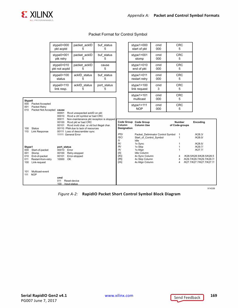
Serial RapidIO Gen2 v4.1 www.xilinx.com 169PG007 June 7, 2017
Appendix A: Packet and Control Symbol Formats
X-Ref Target - Figure A-2
Figure A-2: RapidIO Packet Short Control Symbol Block Diagram
Stype0000 Packet Accepted001 Packet Retry010 Packet Not Accepted
100 Status110 Link Response
Stype1000 Start-of-packet001 Stomp010 End-of-packet011 Restart-from-retry100 Link-request
101 Multicast-event111 NOP
Packet Format for Control Symbol
cause00001 Rcvd unexpected ackID on pkt00010 Rcvd a ctrl symbol w/ bad CRC00011 Non-maintenance pkt reception is stopped00100 Rcvd pkt w/ bad CRC00101 Rcvd invld char. or vld but illegal char.00110 PNA due to lack of resources00111 Loss of descrambler sync11111 General Error
port_status00010 Error00100 Retry-stopped00101 Error-stopped10000 OK
cmd011 Reset-device100 Input-status
Code GroupColumn Designation
/PD//SC//I//K//R//A/||I||||K||||R||||A||
Code GroupColumn Use
Packet_Deliminator Control SymbolStart_of_Control_SymbolIdle1x Sync1x Skip1x AlignIdle Column4x Sync Column4x Skip Column4x Align Column
Number of Code-groups
11
111
444
Encoding
/K28.3//K28.0/
/K28.5//K29.7//K27.7/
/K28.5/K28.5/K28.5/K28.5/K29.7/K29.7/K29.7/K29.7//K27.7/K27.7/K27.7/K27.7/
port_status 5
ackID_status5
stype0=110link resp.
buf_status 5
ackID_status5
stype0=100status
cause 5
packet_ackID5
stype0=010pkt not acptd
buf_status 5
packet_ackID5
stype0=001ptk retry
buf_status 5
packet_ackID5
stype0=000pkt acptd
CRC 5
cmd3
stype1=100link request
CRC 5
cmd000
stype1=011restart retry
CRC 5
cmd000
stype1=010end of pkt
CRC 5
cmd000
stype1=001stomp
CRC 5
cmd000
stype1=000start of pkt
CRC 5
cmd000
stype1=101multicast
CRC 5
cmd000
stype1=111NOP
X14339
Send Feedback
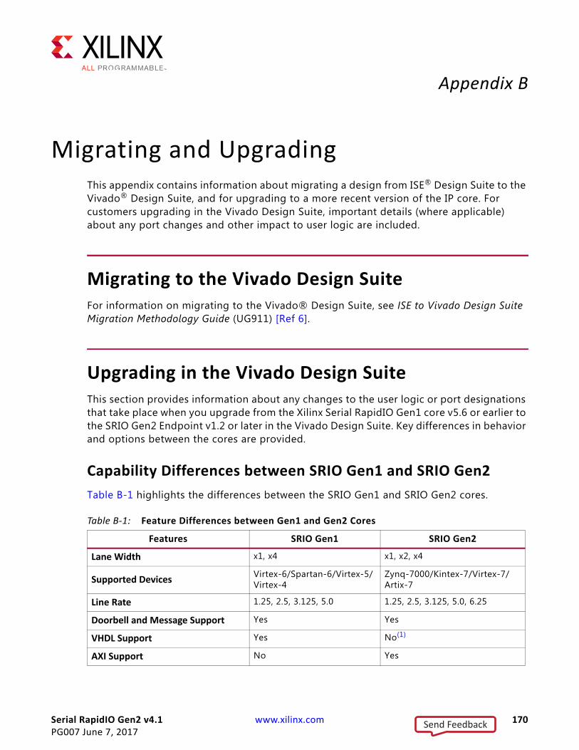
Serial RapidIO Gen2 v4.1 www.xilinx.com 170PG007 June 7, 2017
Appendix B
Migrating and UpgradingThis appendix contains information about migrating a design from ISE® Design Suite to the Vivado® Design Suite, and for upgrading to a more recent version of the IP core. For customers upgrading in the Vivado Design Suite, important details (where applicable) about any port changes and other impact to user logic are included.
Migrating to the Vivado Design SuiteFor information on migrating to the Vivado® Design Suite, see ISE to Vivado Design Suite Migration Methodology Guide (UG911) [Ref 6].
Upgrading in the Vivado Design SuiteThis section provides information about any changes to the user logic or port designations that take place when you upgrade from the Xilinx Serial RapidIO Gen1 core v5.6 or earlier to the SRIO Gen2 Endpoint v1.2 or later in the Vivado Design Suite. Key differences in behavior and options between the cores are provided.
Capability Differences between SRIO Gen1 and SRIO Gen2Table B-1 highlights the differences between the SRIO Gen1 and SRIO Gen2 cores.
Table B-1: Feature Differences between Gen1 and Gen2 Cores
Features SRIO Gen1 SRIO Gen2
Lane Width x1, x4 x1, x2, x4
Supported Devices Virtex-6/Spartan-6/Virtex-5/Virtex-4
Zynq-7000/Kintex-7/Virtex-7/ Artix-7
Line Rate 1.25, 2.5, 3.125, 5.0 1.25, 2.5, 3.125, 5.0, 6.25
Doorbell and Message Support Yes Yes
VHDL Support Yes No(1)
AXI Support No Yes
Send Feedback
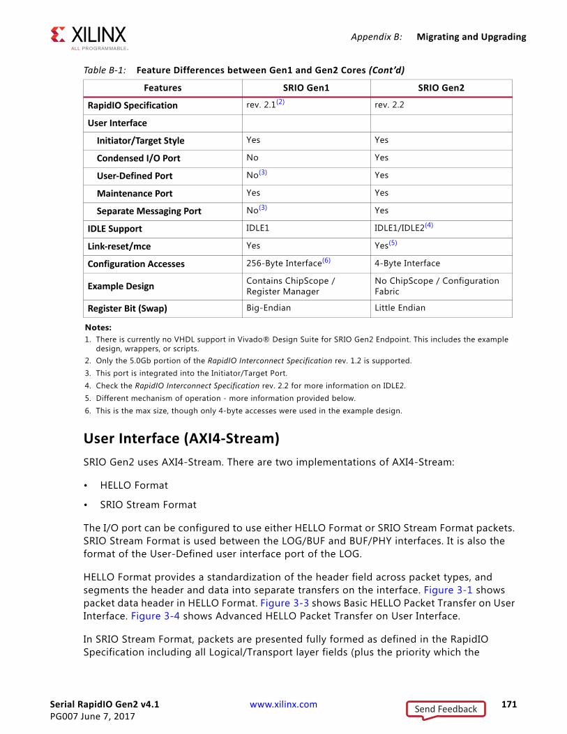
Serial RapidIO Gen2 v4.1 www.xilinx.com 171PG007 June 7, 2017
Appendix B: Migrating and Upgrading
User Interface (AXI4-Stream)SRIO Gen2 uses AXI4-Stream. There are two implementations of AXI4-Stream:
• HELLO Format
• SRIO Stream Format
The I/O port can be configured to use either HELLO Format or SRIO Stream Format packets. SRIO Stream Format is used between the LOG/BUF and BUF/PHY interfaces. It is also the format of the User-Defined user interface port of the LOG.
HELLO Format provides a standardization of the header field across packet types, and segments the header and data into separate transfers on the interface. Figure 3-1 shows packet data header in HELLO Format. Figure 3-3 shows Basic HELLO Packet Transfer on User Interface. Figure 3-4 shows Advanced HELLO Packet Transfer on User Interface.
In SRIO Stream Format, packets are presented fully formed as defined in the RapidIO Specification including all Logical/Transport layer fields (plus the priority which the
RapidIO Specification rev. 2.1(2) rev. 2.2
User Interface
Initiator/Target Style Yes Yes
Condensed I/O Port No Yes
User-Defined Port No(3) Yes
Maintenance Port Yes Yes
Separate Messaging Port No(3) Yes
IDLE Support IDLE1 IDLE1/IDLE2(4)
Link-reset/mce Yes Yes(5)
Configuration Accesses 256-Byte Interface(6) 4-Byte Interface
Example Design Contains ChipScope / Register Manager
No ChipScope / Configuration Fabric
Register Bit (Swap) Big-Endian Little Endian
Notes: 1. There is currently no VHDL support in Vivado® Design Suite for SRIO Gen2 Endpoint. This includes the example
design, wrappers, or scripts. 2. Only the 5.0Gb portion of the RapidIO Interconnect Specification rev. 1.2 is supported. 3. This port is integrated into the Initiator/Target Port.4. Check the RapidIO Interconnect Specification rev. 2.2 for more information on IDLE2.5. Different mechanism of operation - more information provided below.6. This is the max size, though only 4-byte accesses were used in the example design.
Table B-1: Feature Differences between Gen1 and Gen2 Cores (Cont’d)
Features SRIO Gen1 SRIO Gen2
Send Feedback
Serial RapidIO Gen2 v4.1 www.xilinx.com 172PG007 June 7, 2017
Appendix B: Migrating and Upgrading
specification defines as a Physical Layer field). Figure 3-6 shows Basic SRIO Stream Format on User Interface. Figure 3-7 shows Advanced SRIO Stream Format on User Interface.
At the user port in SRIO Gen1, the header information is provided through separate signals in the Initiator Port Signaling Interface described in LogiCORE IP Serial RapidIO User Guide v5.6 (UG503) [Ref 11] or later.
Packet transfer between LOG and BUF and between BUF and PHY occurs through LocalLink interface as described in LogiCORE IP Serial RapidIO v5.6 User Guide (UG503) [Ref 11] or later.
Logical Layer Ports (User Interface)In SRIO Gen1, there is only one user interface where the interface is divided into four separate interfaces from which a packet can be issued or consumed. The interfaces are Initiator Request, Initiator Response, Target Request and Target Response. In SRIO Gen2, the user interface is divided into four different ports:
• I/O port
• Messaging port
• User-Defined port
• Maintenance port
I/O Port
There are two types of I/O port, each of which can be configured in the Vivado Integrated Design Environment (IDE):
• Condensed I/O. This port has only two channels (iotx and iorx) to transmit and receive I/O packets.
• Initiator/Target. This port has four channels to transmit and receive I/O packets: ireq, iresp, treq and tresp, which are similar to the user interface in SRIO Gen1.
All the channels in both ports are AXI4-Stream. Each channel could be configured with either HELLO format or SRIO Stream Format. For a list of signals on these interface channels, see Chapter 2, Product Specification.
Messaging Port
Unlike in SRIO Gen1 where both Message and other packet types are transmitted and received from the same channel, in SRIO Gen2 there is a separate Messaging port with four distinct channels: msgireq, msgiresp, msgtreq and msgtresp. However, it is not restricted to channel all the Message packets through this port, messages can also be combined onto the I/O ports, treated as write transactions. The Messaging port uses either HELLO or SRIO Stream Format.
Send Feedback

Serial RapidIO Gen2 v4.1 www.xilinx.com 173PG007 June 7, 2017
Appendix B: Migrating and Upgrading
User-Defined Port
Another port in the user interface is the User-Defined port with two AXI4-Stream interfaces (txuser and rxuser) that support only SRIO Stream Format. If a received transaction is not supported, it is presented on the User-Defined port. This is an optional port and can be disabled in the Vivado IDE during core configuration.
Maintenance Port
The last port in the user interface is the Maintenance port. This is a separate port in SRIO Gen2 for only maintenance transactions. It has an AXI4-Lite interface that allows the user application to target either the local or remote configuration space. Table 2-7, page 24 lists the AXI4-Lite Maintenance Port signals.
Configuration AccessThis section describes the differences between the configuration access transactions.
Maintenance Transaction
There are two primary differences between SRIO Gen1 and SRIO Gen2 regarding maintenance transaction:
• SRIO Gen1 supports any maintenance transaction size supported by standard NREAD/NWRITE packets. However, SRIO Gen2 only supports 4-byte accesses. The RapidIO Specification rev. 2.2 states that 4-byte accesses should be used. In SRIO Gen1, the max size was 256-byte accesses though only 4-byte accesses were used in the example design.
• While sending remote configuration accesses from SRIO Gen2, the necessary information to set up the header of the outgoing transaction including Destination ID, TID, Priority and CRF are taken from the Maintenance Request Information Register. SRIO Gen2 is used as an endpoint core. Because of this, the core is not responsible for configuring the system so this information would not be used. However, if the core is not used as an endpoint, this register needs to be written to change these fields for each maintenance request. The one exception is TID. The TID increases each subsequent request. When just issuing maintenance requests to the same Destination ID, the Maintenance Request Information Register has to be written only once. In SRIO Gen1, the above information is provided through the Maintenance Port Signaling interface as described in LogiCORE IP Serial RapidIO v5.6 User Guide (UG503) [Ref 11].
Management Interface
SRIO Gen1 uses the register manager and the management interface to access the configuration registers of the core. In SRIO Gen2, the management interface has been replaced with AXI4-Lite interface which is referred as configuration interface. The
Send Feedback
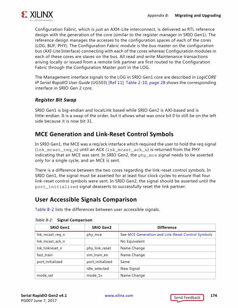
Serial RapidIO Gen2 v4.1 www.xilinx.com 174PG007 June 7, 2017
Appendix B: Migrating and Upgrading
Configuration Fabric, which is just an AXI4-Lite interconnect, is delivered as RTL reference design with the generation of the core (similar to the register manager in SRIO Gen1). The reference design manages the accesses to the configuration spaces of each of the cores (LOG, BUF, PHY). The Configuration Fabric module is the bus master on the configuration bus (AXI-Lite Interface) connecting with each of the cores whereas Configuration modules in each of these cores are slaves on the bus. All read and write Maintenance transactions arising locally or issued from a remote link partner are first routed to the Configuration Fabric through the Configuration Master port in the LOG.
The Management interface signals to the LOG in SRIO Gen1 core are described in LogiCORE IP Serial RapidIO User Guide (UG503) [Ref 11]. Table 2-10, page 28 shows the corresponding interface in SRIO Gen 2 core.
Register Bit Swap
SRIO Gen1 is big-endian and localLink based while SRIO Gen2 is AXI-based and is little-endian. It is a swap of the order, but it allows what was once bit 0 to still be on the left side because it is now bit 31.
MCE Generation and Link-Reset Control SymbolsIn SRIO Gen1, the MCE was a req/ack interface which required the user to hold the req signal (lnk_mcast_req_n) until an ACK (lnk_mcast_ack_n) is returned from the PHY indicating that an MCE was sent. In SRIO Gen2, the phy_mce signal needs to be asserted only for a single cycle, and an MCE is sent.
There is a difference between the two cores regarding the link-reset control symbols. In SRIO Gen1, the signal must be asserted for at least four clock cycles to ensure that four link-reset control symbols were sent. In SRIO Gen2, the signal should be asserted until the port_initialized signal deasserts to successfully reset the link partner.
User Accessible Signals ComparisonTable B-2 lists the differences between user accessible signals.
Table B-2: Signal Comparison
SRIO Gen1 SRIO Gen2 Difference
lnk_mcast_req_n phy_mce See MCE Generation and Link-Reset Control Symbols
lnk_mcast_ack_n No Equivalent
lnk_linkreset_n phy_link_reset Name Change
fast_train sim_train_en Name Change
port_initialized port_initialized Same
idle_selected New Signal
mode_sel mode_1x Name Change
Send Feedback

Serial RapidIO Gen2 v4.1 www.xilinx.com 175PG007 June 7, 2017
Appendix B: Migrating and Upgrading
Clocking and ResetThis section describes the differences in the clock and reset functionality.
LOG Layer
Table B-3 details the differences in the LOG Layer.
BUF Layer
Table B-4 details the differences in the LOG Layer.
lnk_trdy_n/lnk_rrdy_n link_initialized Name Change
lnk_porterr_n port_error Name Change
resp_time_out port_timeout Name Change
Table B-3: LOG Layer Comparison
SRIO Gen1 SRIO Gen2 Difference
clk(1) log_clk(2) Name Change; Functional Difference
reset_n log_rst Name Change
mgt_clk cfg_clk(2) Name Change; Functional Difference
mgt_reset_n cfg_rst Name Change; Functional Difference
Notes: 1. For clock frequencies at different line rates and 1x/4x mode, see LogiCORE IP Serial RapidIO v5.6 User Guide
(UG503) [Ref 11].2. Check Table 3-4, page 92 through Table 3-6, page 92 for clock frequencies at different line rates and 1x/4x mode.
Table B-4: BUF Layer Comparison
SRIO Gen1 SRIO Gen2 Difference
log_clk(1) log_clk(1) Same Name; Functional Difference
log_reset_n No Equivalent
phy_clk(1) phy_clk(1) Same Name; Functional Difference
phy_reset_n No Equivalent
buf_rst New Signal
mgt_clk cfg_clk(1) Name Change; Functional Difference
mgt_rst_n cfg_rst Name Change; Functional Difference
Notes: 1. For clock frequencies at different line rates and 1x/4x mode, see LogiCORE IP Serial RapidIO v5.6 User Guide
(UG503) [Ref 11].2. Check Table 3-4, page 92 through Table 3-6, page 92 for clock frequencies at different line rates and 1x/4x mode.
Table B-2: Signal Comparison (Cont’d)
SRIO Gen1 SRIO Gen2 Difference
Send Feedback
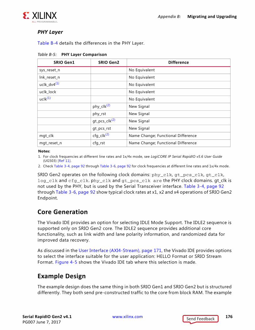
Serial RapidIO Gen2 v4.1 www.xilinx.com 176PG007 June 7, 2017
Appendix B: Migrating and Upgrading
PHY Layer
Table B-4 details the differences in the PHY Layer.
SRIO Gen2 operates on the following clock domains: phy_clk, gt_pcs_clk, gt_clk, log_clk and cfg_clk. phy_clk and gt_pcs_clk are the PHY clock domains. gt_clk is not used by the PHY, but is used by the Serial Transceiver interface. Table 3-4, page 92 through Table 3-6, page 92 show typical clock rates at x1, x2 and x4 operations of SRIO Gen2 Endpoint.
Core GenerationThe Vivado IDE provides an option for selecting IDLE Mode Support. The IDLE2 sequence is supported only on SRIO Gen2 core. The IDLE2 sequence provides additional core functionality, such as link width and lane polarity information, and randomized data for improved data recovery.
As discussed in the User Interface (AXI4-Stream), page 171, the Vivado IDE provides options to select the interface suitable for the user application: HELLO Format or SRIO Stream Format. Figure 4-5 shows the Vivado IDE tab where this selection is made.
Example DesignThe example design does the same thing in both SRIO Gen1 and SRIO Gen2 but is structured differently. They both send pre-constructed traffic to the core from block RAM. The example
Table B-5: PHY Layer Comparison
SRIO Gen1 SRIO Gen2 Difference
sys_reset_n No Equivalent
lnk_reset_n No Equivalent
uclk_dv4(1) No Equivalent
uclk_lock No Equivalent
uclk(1) No Equivalent
phy_clk(2) New Signal
phy_rst New Signal
gt_pcs_clk(2) New Signal
gt_pcs_rst New Signal
mgt_clk cfg_clk(2) Name Change; Functional Difference
mgt_reset_n cfg_rst Name Change; Functional Difference
Notes: 1. For clock frequencies at different line rates and 1x/4x mode, see LogiCORE IP Serial RapidIO v5.6 User Guide
(UG503) [Ref 11].2. Check Table 3-4, page 92 through Table 3-6, page 92 for clock frequencies at different line rates and 1x/4x mode.
Send Feedback

Serial RapidIO Gen2 v4.1 www.xilinx.com 177PG007 June 7, 2017
Appendix B: Migrating and Upgrading
design in the SRIO Gen1 core has more logic for ChipScope tools. For the current Gen2 core, there is no Vivado Design Suite debug feature functionality. In addition, SRIO Gen1 provides a Register Manager, which is replaced in SRIO Gen2 by the Configuration Fabric.
Send Feedback
Serial RapidIO Gen2 v4.1 www.xilinx.com 178PG007 June 7, 2017
Appendix C
DebuggingThis appendix provides information for using the resources available on the Xilinx Support website, and debugging tools.
TIP: If the IP generation halts with an error, there might be a license issue. See License Checkers in Chapter 1 for more details.
Finding Help on Xilinx.comTo help in the design and debug process when using the SRIO Gen2 core, the Xilinx Support web page contains key resources such as product documentation, release notes, answer records, information about known issues, and links for obtaining further product support.
DocumentationThis product guide is the main document associated with the SRIO Gen2 core. This guide, along with documentation related to all products that aid in the design process, can be found on the Xilinx Support web page or by using the Xilinx Documentation Navigator.
You can download the Xilinx Documentation Navigator from the Downloads page. For more information about this tool and the features available, open the online help after installation.
Answer RecordsAnswer Records include information about commonly encountered problems, helpful information on how to resolve these problems, and any known issues with a Xilinx product. Answer Records are created and maintained daily ensuring that users have access to the most accurate information available.
Send Feedback
Serial RapidIO Gen2 v4.1 www.xilinx.com 179PG007 June 7, 2017
Appendix C: Debugging
Answer Records for this core can be located by using the Search Support box on the main Xilinx support web page. To maximize your search results, use proper keywords such as:
• the product name
• tool messages
• summary of the issue encountered
A filter search is available after results are returned to further target the results.
Answer Records for the SRIO Gen2 Core
AR: 54648
Technical SupportXilinx provides technical support in the Xilinx Support web page for this LogiCORE™ IP product when used as described in the product documentation. Xilinx cannot guarantee timing, functionality, or support if you do any of the following:
• Implement the solution in devices that are not defined in the documentation.
• Customize the solution beyond that allowed in the product documentation.
• Change any section of the design labeled DO NOT MODIFY.
Xilinx provides premier technical support for customers encountering issues that require additional assistance. To contact Xilinx Technical Support, navigate to the Xilinx Support web page.
Send Feedback

Serial RapidIO Gen2 v4.1 www.xilinx.com 180PG007 June 7, 2017
Appendix C: Debugging
Debug ToolsThere are many tools available to address SRIO Gen2 design issues. It is important to know which tools are useful for debugging various situations.
Vivado Design Suite Debug FeatureThe Vivado® Design Suite debug feature inserts logic analyzer and virtual I/O cores directly into your design. The debug feature also allows you to set trigger conditions to capture application and integrated block port signals in hardware. Captured signals can then be analyzed. This feature represents the functionality in the Vivado Integrated Design Environment (IDE) that is used for logic debugging and validation of a design running in Xilinx devices in hardware.
The Vivado logic analyzer is used to interact with the logic debug LogiCORE IP cores, including:
• ILA 2.0 (and later versions)
• VIO 2.0 (and later versions)
See Vivado Design Suite User Guide: Programming and Debugging (UG908) [Ref 8].
Reference BoardsVarious Xilinx development boards support theSRIO Gen2. These boards can be used to prototype designs and establish that the core can communicate with the system.
• 7 series evaluation boards
° KC705
° KC724
Waveform Analysis and Debug
Link InitializationWhen debugging link issues, start by checking that the following SRIO Gen2 top-level wrapper signals are toggling properly. Including, but not limited to:
• reset
• clk_lock
Send Feedback
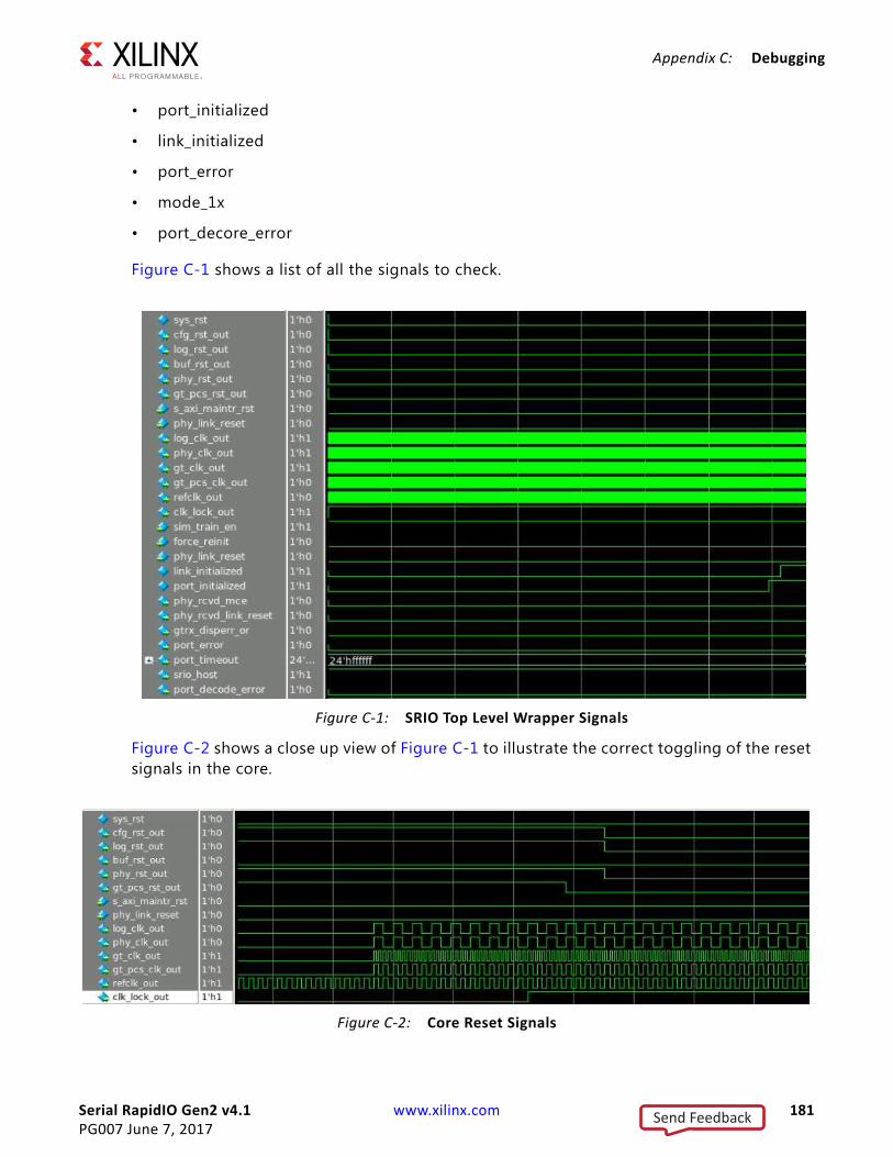
Serial RapidIO Gen2 v4.1 www.xilinx.com 181PG007 June 7, 2017
Appendix C: Debugging
• port_initialized
• link_initialized
• port_error
• mode_1x
• port_decore_error
Figure C-1 shows a list of all the signals to check.
Figure C-2 shows a close up view of Figure C-1 to illustrate the correct toggling of the reset signals in the core.
X-Ref Target - Figure C-1
Figure C-1: SRIO Top Level Wrapper Signals
X-Ref Target - Figure C-2
Figure C-2: Core Reset Signals
Send Feedback
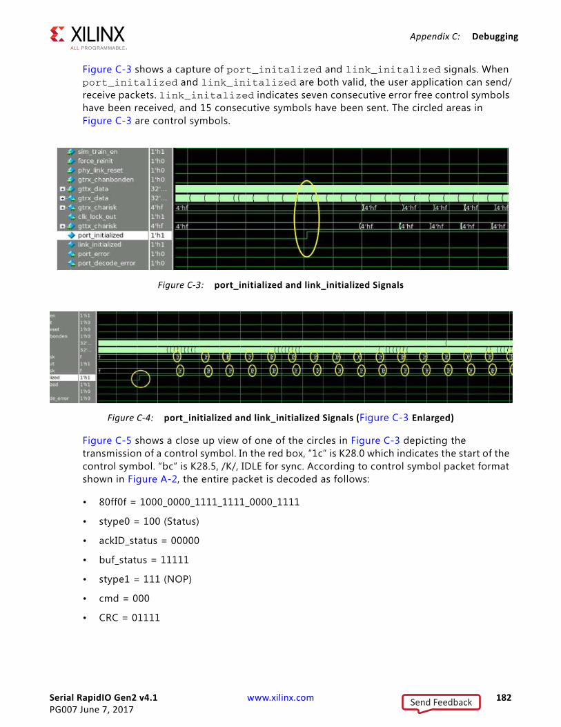
Serial RapidIO Gen2 v4.1 www.xilinx.com 182PG007 June 7, 2017
Appendix C: Debugging
Figure C-3 shows a capture of port_initalized and link_initalized signals. When port_initalized and link_initalized are both valid, the user application can send/receive packets. link_initalized indicates seven consecutive error free control symbols have been received, and 15 consecutive symbols have been sent. The circled areas in Figure C-3 are control symbols.
Figure C-5 shows a close up view of one of the circles in Figure C-3 depicting the transmission of a control symbol. In the red box, “1c” is K28.0 which indicates the start of the control symbol. “bc” is K28.5, /K/, IDLE for sync. According to control symbol packet format shown in Figure A-2, the entire packet is decoded as follows:
• 80ff0f = 1000_0000_1111_1111_0000_1111
• stype0 = 100 (Status)
• ackID_status = 00000
• buf_status = 11111
• stype1 = 111 (NOP)
• cmd = 000
• CRC = 01111
X-Ref Target - Figure C-3
Figure C-3: port_initialized and link_initialized Signals
X-Ref Target - Figure C-4
Figure C-4: port_initialized and link_initialized Signals (Figure C-3 Enlarged)
Send Feedback

Serial RapidIO Gen2 v4.1 www.xilinx.com 183PG007 June 7, 2017
Appendix C: Debugging
If the initialization does not complete (port_initialized and link_initalized signals are not asserted), check GT_RXDATA to confirm that IDLE (bcfd) ordered sets are being received and also check for any coding errors. This can be done by looking at RXNOTINTABLE which should always be '0'.
Ensure all the signals on the serial transceiver (GT) interface are toggling correctly. Figure C-6 shows those signals.
SWRITE Packet AnalysisFigure C-7 shows a SWRITE Packet sent to the IREQ Interface, the data on s_axis_ireq_tdata is 0060200000000777_0000000000000000.
X-Ref Target - Figure C-5
Figure C-5: Control Symbol Before Assertion of link_initialized Signal
X-Ref Target - Figure C-6
Figure C-6: GT Interface Signals
Send Feedback
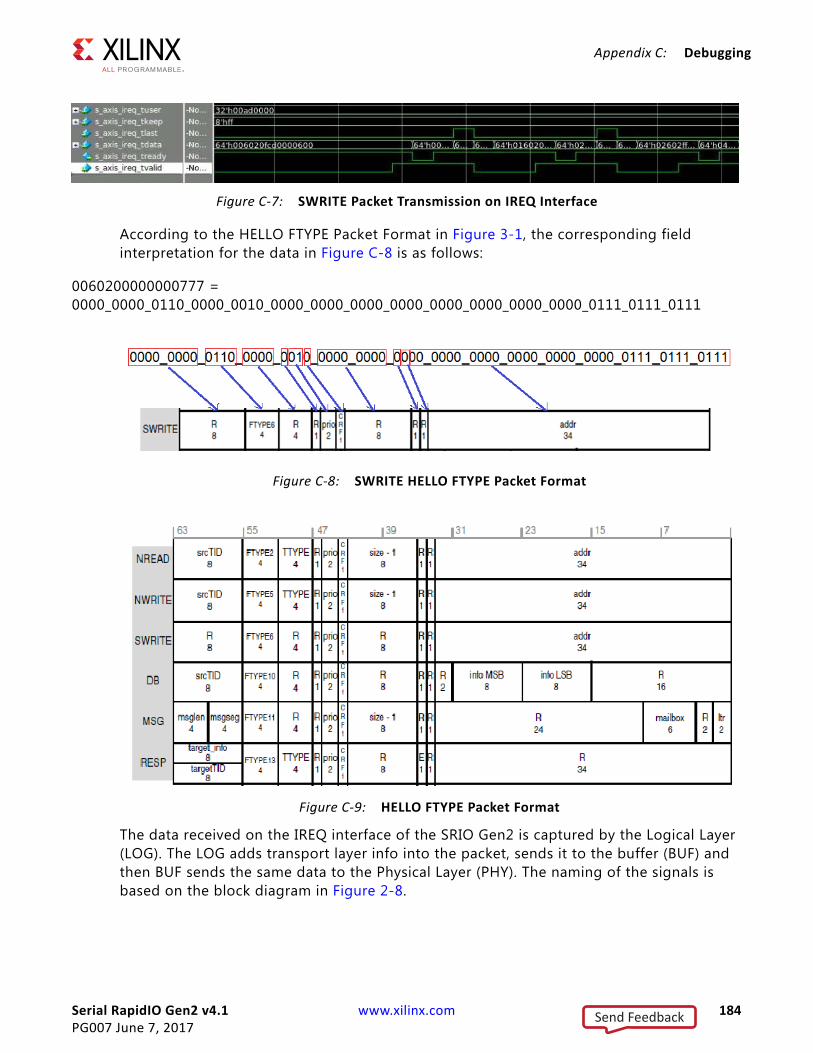
Serial RapidIO Gen2 v4.1 www.xilinx.com 184PG007 June 7, 2017
Appendix C: Debugging
According to the HELLO FTYPE Packet Format in Figure 3-1, the corresponding field interpretation for the data in Figure C-8 is as follows:
0060200000000777 = 0000_0000_0110_0000_0010_0000_0000_0000_0000_0000_0000_0000_0000_0111_0111_0111
The data received on the IREQ interface of the SRIO Gen2 is captured by the Logical Layer (LOG). The LOG adds transport layer info into the packet, sends it to the buffer (BUF) and then BUF sends the same data to the Physical Layer (PHY). The naming of the signals is based on the block diagram in Figure 2-8.
X-Ref Target - Figure C-7
Figure C-7: SWRITE Packet Transmission on IREQ Interface
X-Ref Target - Figure C-8
Figure C-8: SWRITE HELLO FTYPE Packet FormatX-Ref Target - Figure C-9
Figure C-9: HELLO FTYPE Packet Format
Send Feedback

Serial RapidIO Gen2 v4.1 www.xilinx.com 185PG007 June 7, 2017
Appendix C: Debugging
Figure C-11 and Figure C-12 show the same data “0070070000ff0046_0000000000000000” being passed from the Transport interface to Link interface of the BUF.
Figure C-13 shows a simulation capture of all three interfaces discussed.
X-Ref Target - Figure C-10
Figure C-10: SWRITE Packet Transmission on IREQ, LOG to BUF and BUF to PHY
X-Ref Target - Figure C-11
Figure C-11: SWRITE Packet from LOG to BUFX-Ref Target - Figure C-12
Figure C-12: SWRITE Packet from BUF to PHY
Send Feedback

Serial RapidIO Gen2 v4.1 www.xilinx.com 186PG007 June 7, 2017
Appendix C: Debugging
The BUF transmits the packet coming from the LOG to the PHY. The PHY adds PHY layer info and sends the packet to the GT. Figure C-14 shows the SWRITE packet traveling from the IREQ to the GT interface. The four cursors in the waveform show the start of the packet in each interface.
To view the packet on the GT interface, check gttx_data. As shown in Figure C-14, the entire packet transmitted from PHY to GT consists of:
7c96f818_ b04600ff_00000770_00000000_00000000_34b70000_7c97fa1b
X-Ref Target - Figure C-13
Figure C-13: SWRITE Packet from IREQ to GT Interface
X-Ref Target - Figure C-14
Figure C-14: SWRITE Packet Transmission on GT Interface
Send Feedback

Serial RapidIO Gen2 v4.1 www.xilinx.com 187PG007 June 7, 2017
Appendix C: Debugging
The Start of Packet (SOP) is 7c96f818. 7c indicates the packet deliminator control symbol. The rest of the packet is decoded as follows (also illustrated in Figure C-15):
96f818 = 1001_0110_1111_1000_0001_1000
• 100 = Status
• 10110 = ackID 16
• 11111 = buf_status
• 000 = SOP
• 000 = cmd
• 11000 = CRC
The SWRITE packet = b04600ff 00000770 with write data of all 0s (64bits). This is decoded as follows (also illustrated in Figure C-16):
b04600ff 00000770 = 1011_0000_0100_0110_0000_0000_1111_1111_0000_0000_0000_0000_0000_0111_0111 0000
• ackID = 10110 (16)
• rsvd = 00
• crf = 0
• prio = 01
• tt = 00
X-Ref Target - Figure C-15
Figure C-15: Packet Deliminator Control Symbol (SOP) Analysis
Send Feedback
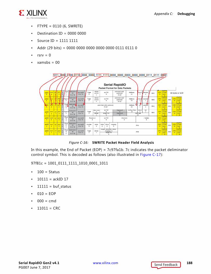
Serial RapidIO Gen2 v4.1 www.xilinx.com 188PG007 June 7, 2017
Appendix C: Debugging
• FTYPE = 0110 (6, SWRITE)
• Destination ID = 0000 0000
• Source ID = 1111 1111
• Addr (29 bits) = 0000 0000 0000 0000 0000 0111 0111 0
• rsrv = 0
• xamsbs = 00
In this example, the End of Packet (EOP) = 7c97fa1b. 7c indicates the packet deliminator control symbol. This is decoded as follows (also illustrated in Figure C-17):
97f81c = 1001_0111_1111_1010_0001_1011
• 100 = Status
• 10111 = ackID 17
• 11111 = buf_status
• 010 = EOP
• 000 = cmd
• 11011 = CRC
X-Ref Target - Figure C-16
Figure C-16: SWRITE Packet Header Field Analysis
Send Feedback
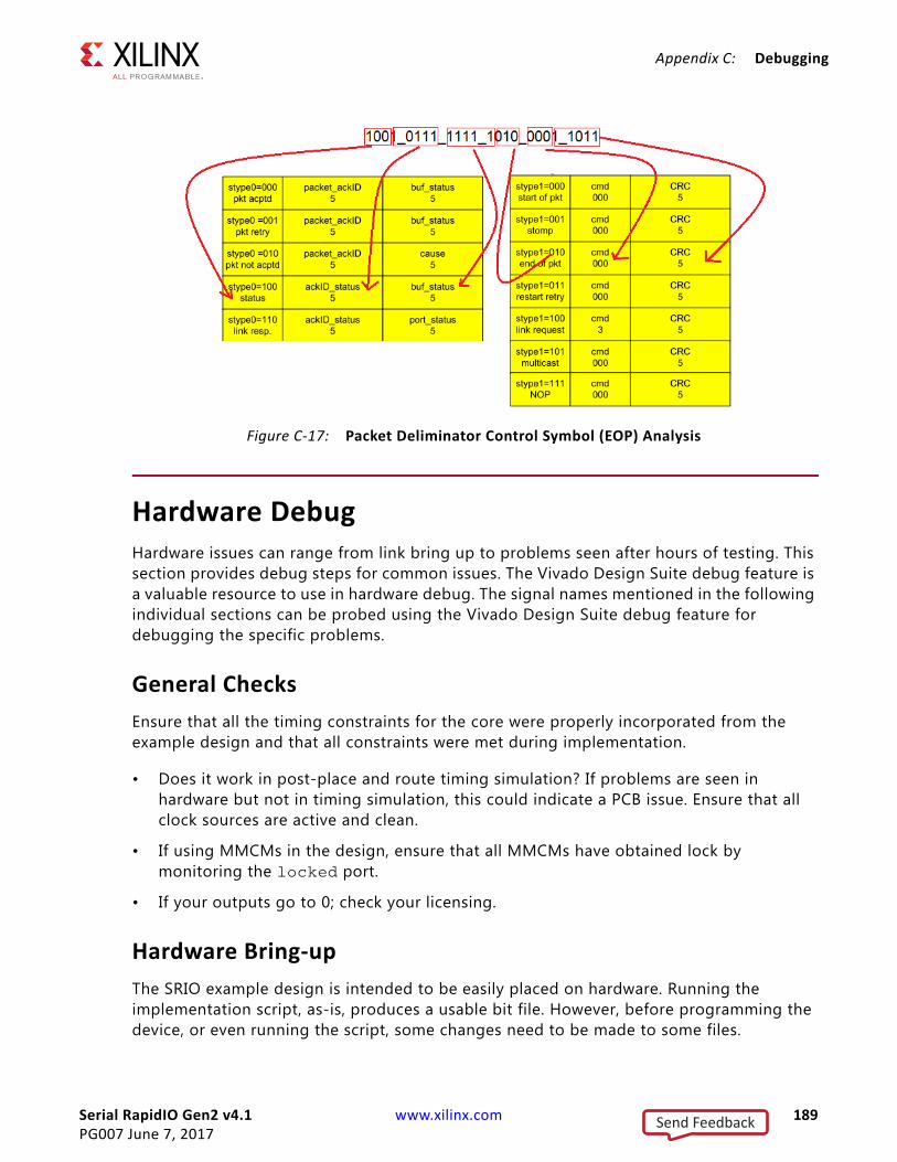
Serial RapidIO Gen2 v4.1 www.xilinx.com 189PG007 June 7, 2017
Appendix C: Debugging
Hardware DebugHardware issues can range from link bring up to problems seen after hours of testing. This section provides debug steps for common issues. The Vivado Design Suite debug feature is a valuable resource to use in hardware debug. The signal names mentioned in the following individual sections can be probed using the Vivado Design Suite debug feature for debugging the specific problems.
General ChecksEnsure that all the timing constraints for the core were properly incorporated from the example design and that all constraints were met during implementation.
• Does it work in post-place and route timing simulation? If problems are seen in hardware but not in timing simulation, this could indicate a PCB issue. Ensure that all clock sources are active and clean.
• If using MMCMs in the design, ensure that all MMCMs have obtained lock by monitoring the locked port.
• If your outputs go to 0; check your licensing.
Hardware Bring-upThe SRIO example design is intended to be easily placed on hardware. Running the implementation script, as-is, produces a usable bit file. However, before programming the device, or even running the script, some changes need to be made to some files.
X-Ref Target - Figure C-17
Figure C-17: Packet Deliminator Control Symbol (EOP) Analysis
Send Feedback

Serial RapidIO Gen2 v4.1 www.xilinx.com 190PG007 June 7, 2017
Appendix C: Debugging
Part Selection
If the wrong device is targeted during implementation, the bit file does not download to the device properly. The device is selected when creating the project, and the part selected at the beginning of the project creation propagates all the way through to the bit file generation step.
Pin Placement
See the applicable board schematic and supporting documents for proper pin placement. All pins, though there are few in the example design, need to be evaluated for placement.
Edit the Xilinx design constraints (XDC) file and select the proper pins according to the board. Pay special attention to the clock pin, which must be placed on a MGTREFCLK site and must follow placement rules in relation to the transceivers.
The high-speed I/O must also be placed with care. Select transceivers all within the same bank. For the higher line rates (5 Gb/s, 6.25 Gb/s), select transceivers in centralized banks on the right side of the chip for improved timing.
IMPORTANT: Do not modify the IOSTANDARD constraints or the timing constraints. If there are area groups, they should be removed or positioned to a natural location in relation to the new pin selections.
Clock Generation and Other Inputs
sys_clkp/n is expected to be either a 125 MHz or 156.25 MHz free-running differential pair clock. The actual frequency depends on what was selected during core generation. See the appropriate transceiver user guide for jitter tolerances and other requirements.
The reset input is an active-High reset and can be connected to any general I/O pin or user-driven logic. For easy hardware bringup, connect the reset to a debounced pushbutton. Early on, connect the reset to a debounced pushbutton.
Disabling Automatic Packet Generation
Because the example design can be used for both simulation and hardware, it is configured to automatically send packets. This might not be desirable when doing hardware testing. To disable request packets, open instruction_list.vh and set NUMBER_OF_INSTRUCTIONS to 0.
The core also automatically configures both endpoints through maintenance packets. The set of provided configuration packets might not be the endpoints needed for a specific design. Prior to hardware testing, modify the set of instructions in maintenance_list.vh. Alternatively, disable automatic configuration by setting NUMBER_OF_INSTRUCTIONS to 0 in srio_quick_start.v and issue the maintenance instructions through the Vivado Design Suite debug feature.
Send Feedback
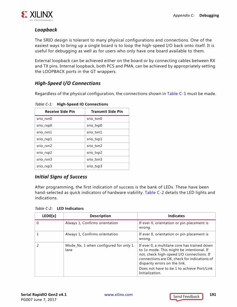
Serial RapidIO Gen2 v4.1 www.xilinx.com 191PG007 June 7, 2017
Appendix C: Debugging
Loopback
The SRIO design is tolerant to many physical configurations and connections. One of the easiest ways to bring up a single board is to loop the high-speed I/O back onto itself. It is useful for debugging as well as for users who only have one board available to them.
External loopback can be achieved either on the board or by connecting cables between RX and TX pins. Internal loopback, both PCS and PMA, can be achieved by appropriately setting the LOOPBACK ports in the GT wrappers.
High-Speed I/O Connections
Regardless of the physical configuration, the connections shown in Table C-1 must be made.
Initial Signs of Success
After programming, the first indication of success is the bank of LEDs. These have been hand-selected as quick indicators of hardware viability. Table C-2 details the LED lights and indications.
Table C-1: High-Speed IO Connections
Receive Side Pin Transmit Side Pin
srio_rxn0 srio_txn0
srio_rxp0 srio_txp0
srio_rxn1 srio_txn1
srio_rxp1 srio_txp1
srio_rxn2 srio_txn2
srio_rxp2 srio_txp2
srio_rxn3 srio_txn3
srio_rxp3 srio_txp3
Table C-2: LED Indicators
LED0[x] Description Indicates
0 Always 1, Confirms orientation If ever 0, orientation or pin placement is wrong.
1 Always 1, Confirms orientation If ever 0, orientation or pin placement is wrong.
2 Mode_Nx, 1 when configured for only 1 lane
If ever 0, a multilane core has trained down to 1x mode. This might be intentional. If not, check high-speed I/O connections. If connections are OK, check for indications of disparity errors on the link. Does not have to be 1 to achieve Port/Link Initialization.
Send Feedback
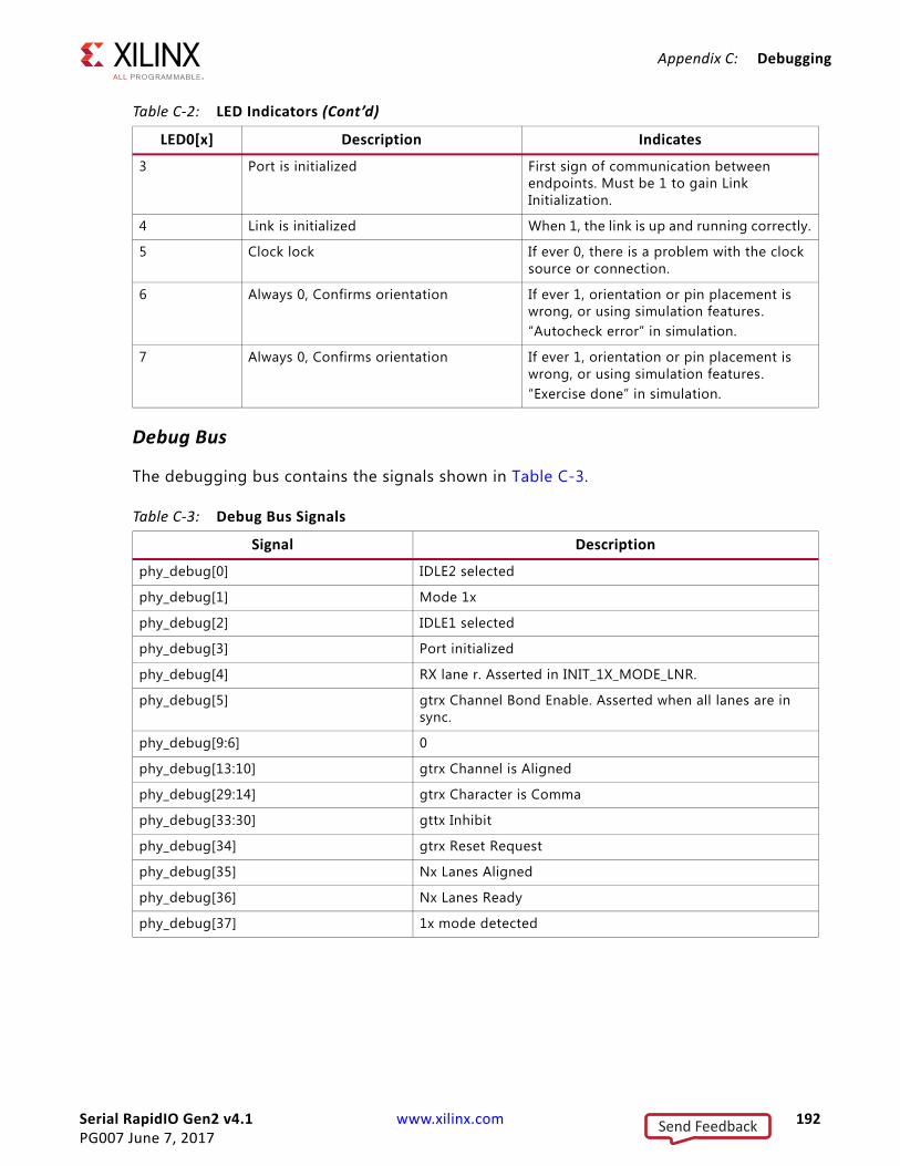
Serial RapidIO Gen2 v4.1 www.xilinx.com 192PG007 June 7, 2017
Appendix C: Debugging
Debug Bus
The debugging bus contains the signals shown in Table C-3.
3 Port is initialized First sign of communication between endpoints. Must be 1 to gain Link Initialization.
4 Link is initialized When 1, the link is up and running correctly.
5 Clock lock If ever 0, there is a problem with the clock source or connection.
6 Always 0, Confirms orientation If ever 1, orientation or pin placement is wrong, or using simulation features.“Autocheck error” in simulation.
7 Always 0, Confirms orientation If ever 1, orientation or pin placement is wrong, or using simulation features.“Exercise done” in simulation.
Table C-3: Debug Bus Signals
Signal Description
phy_debug[0] IDLE2 selected
phy_debug[1] Mode 1x
phy_debug[2] IDLE1 selected
phy_debug[3] Port initialized
phy_debug[4] RX lane r. Asserted in INIT_1X_MODE_LNR.
phy_debug[5] gtrx Channel Bond Enable. Asserted when all lanes are in sync.
phy_debug[9:6] 0
phy_debug[13:10] gtrx Channel is Aligned
phy_debug[29:14] gtrx Character is Comma
phy_debug[33:30] gttx Inhibit
phy_debug[34] gtrx Reset Request
phy_debug[35] Nx Lanes Aligned
phy_debug[36] Nx Lanes Ready
phy_debug[37] 1x mode detected
Table C-2: LED Indicators (Cont’d)
LED0[x] Description Indicates
Send Feedback
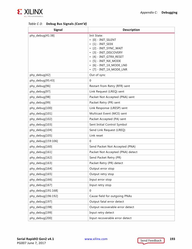
Serial RapidIO Gen2 v4.1 www.xilinx.com 193PG007 June 7, 2017
Appendix C: Debugging
phy_debug[41:38] Init State:• [0] - INIT_SILENT• [1] - INIT_SEEK• [2] - INIT_SYNC_WAIT• [3] - INIT_DISCOVERY• [4] - INIT_GTRX_RESET• [5] - INIT_NX_MODE• [6] - INIT_1X_MODE_LN0• [7] - INIT_1X_MODE_LNR
phy_debug[42] Out of sync
phy_debug[95:43] 0
phy_debug[96] Restart from Retry (RFR) sent
phy_debug[97] Link Request (LREQ) sent
phy_debug[98] Packet Not Accepted (PNA) sent
phy_debug[99] Packet Retry (PR) sent
phy_debug[100] Link Response (LRESP) sent
phy_debug[101] Multicast Event (MCE) sent
phy_debug[102] Packet Accepted (PA) sent
phy_debug[103] Sent Initial Control Symbol
phy_debug[104] Send Link Request (LREQ)
phy_debug[105] Link reset
phy_debug[159:106] 0
phy_debug[160] Send Packet Not Accepted (PNA)
phy_debug[161] Packet Not Accepted (PNA) detect
phy_debug[162] Send Packet Retry (PR)
phy_debug[163] Packet Retry (PR) detect
phy_debug[164] Output error stop
phy_debug[165] Output retry stop
phy_debug[166] Input error stop
phy_debug[167] Input retry stop
phy_debug[191:168] 0
phy_debug[196:192] Cause field for outgoing PNAs
phy_debug[197] Output fatal error detect
phy_debug[198] Output recoverable error detect
phy_debug[199] Input retry detect
phy_debug[200] Input recoverable error detect
Table C-3: Debug Bus Signals (Cont’d)
Signal Description
Send Feedback
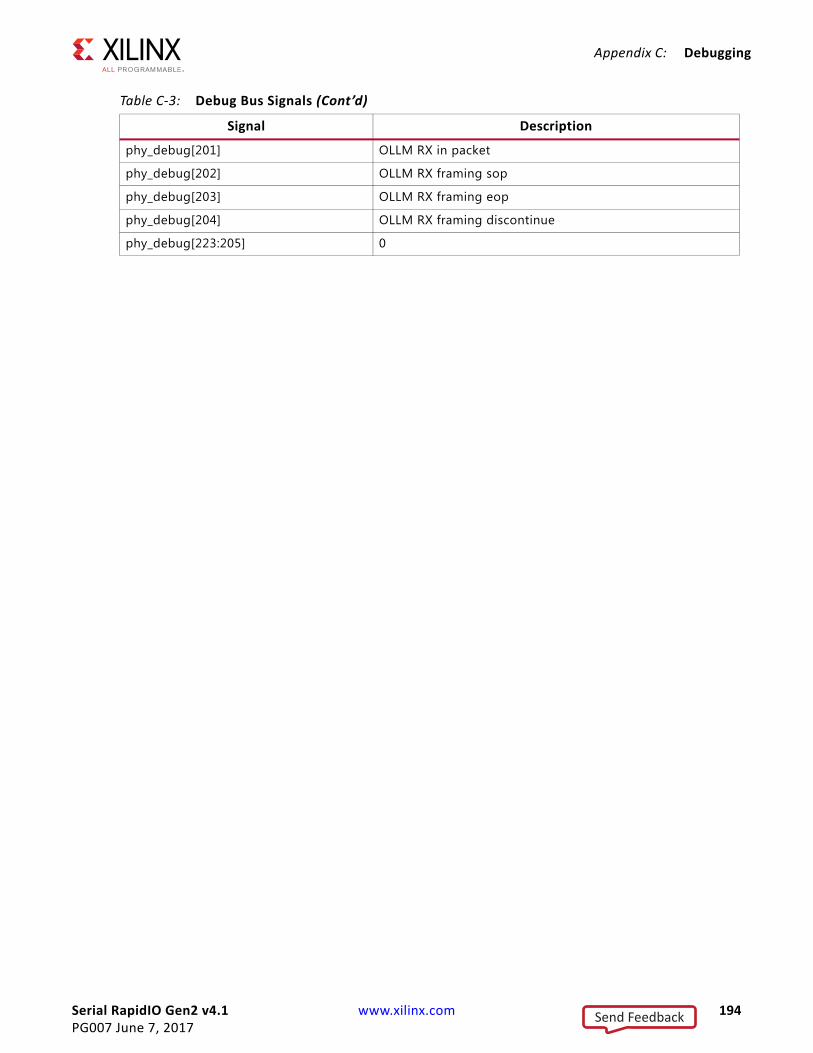
Serial RapidIO Gen2 v4.1 www.xilinx.com 194PG007 June 7, 2017
Appendix C: Debugging
phy_debug[201] OLLM RX in packet
phy_debug[202] OLLM RX framing sop
phy_debug[203] OLLM RX framing eop
phy_debug[204] OLLM RX framing discontinue
phy_debug[223:205] 0
Table C-3: Debug Bus Signals (Cont’d)
Signal Description
Send Feedback
Serial RapidIO Gen2 v4.1 www.xilinx.com 195PG007 June 7, 2017
Appendix D
Additional Resources and Legal Notices
Xilinx ResourcesFor support resources such as Answers, Documentation, Downloads, and Forums, see Xilinx Support.
ReferencesThese documents provide supplemental material:
1. Xilinx Vivado AXI Reference Guide (UG1037)
2. Xilinx Timing Constraints User Guide (UG612)
3. Vivado Design Suite User Guide: Designing with IP (UG896)
4. Vivado Design Suite User Guide: Designing IP Subsystems using IP Integrator (UG994)
5. Vivado Design Suite User Guide: Getting Started (UG910)
6. ISE to Vivado Design Suite Migration Methodology Guide (UG911)
7. Vivado Design Suite User Guide: Logic Simulation (UG900)
8. Vivado Design Suite User Guide: Programming and Debugging (UG908)
9. 7 Series FPGAs GTX/GTH Transceivers User Guide (UG476)
10. 7 Series FPGAs GTP Transceivers User Guide (UG482)
11. LogiCORE IP Serial RapidIO v5.6 User Guide (UG503)
12. LogiCORE IP Serial RapidIO Gen2 - Debugging and Packet Analysis Guide (AR 51066)
13. Serial RapidIO Specifications, www.rapidio.org/specs/current
14. RapidIO Interconnect Specification - Part VI: Physical Layer 1x/4x LP-Serial Specification, www.rapidio.org/data/specs/SerialSpec_v_1pt2.pdf
15. AMBA AXI4-Stream Protocol Specification, http://infocenter.arm.com/help/index.jsp?topic=/com.arm.doc.ihi0051a/index.html
Send Feedback
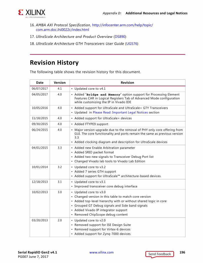
Serial RapidIO Gen2 v4.1 www.xilinx.com 196PG007 June 7, 2017
Appendix D: Additional Resources and Legal Notices
16. AMBA AXI Protocol Specification, http://infocenter.arm.com/help/topic/com.arm.doc.ihi0022c/index.html
17. UltraScale Architecture and Product Overview (DS890)
18. UltraScale Architecture GTH Transceivers User Guide (UG576)
Revision HistoryThe following table shows the revision history for this document.
Date Version Revision
06/07/2017 4.1 • Updated core to v4.1
04/05/2017 4.0 • Added “Bridge and Memory” option support for Processing Element Features CAR in Logical Registers Tab of Advanced Mode configuration while customizing the IP in Vivado IDE
10/05/2016 4.0 • Added support for UltraScale and UltraScale+ GTY Transceivers• Updated in Please Read: Important Legal Notices section
11/18/2015 4.0 • Added support for UltraScale+ devices
09/30/2015 4.0 • Added FTYPE9 support
06/24/2015 4.0 • Major version upgrade due to the removal of PHY only core offering from GUI. The core functionality and ports remain the same as previous version 3.3
• Added clocking diagram and description for UltraScale devices
04/01/2015 3.3 • Added new Enable Arbitration parameter• Added SRIO packet format• Added two new signals to Transceiver Debug Port list• Changed Vivado lab tools to Vivado Lab Edition
10/01/2014 3.2 • Updated core to v3.2• Added 7 series GTH support• Added support for UltraScale™ architecture-based devices
12/18/2013 3.1 • Updated core to v3.1• Improved transceiver core debug interface
10/02/2013 3.0 • Updated core to v3.0• Changed version in this table to match core version• Added top-level hierarchy with or without shared logic in core• Grouped GT Debug signals and Side band signals• Added Vivado IP integrator support• Removed ChipScope debug content
03/20/2013 2.0 • Updated core to v2.0• Removed support for ISE Design Suite• Removed support for Virtex-6 devices• Added support for Zynq-7000 devices
Send Feedback
Serial RapidIO Gen2 v4.1 www.xilinx.com 197PG007 June 7, 2017
Appendix D: Additional Resources and Legal Notices
Please Read: Important Legal NoticesThe information disclosed to you hereunder (the "Materials") is provided solely for the selection and use of Xilinx products. To the maximum extent permitted by applicable law: (1) Materials are made available "AS IS" and with all faults, Xilinx hereby DISCLAIMS ALL WARRANTIES AND CONDITIONS, EXPRESS, IMPLIED, OR STATUTORY, INCLUDING BUT NOT LIMITED TO WARRANTIES OF MERCHANTABILITY, NON-INFRINGEMENT, OR FITNESS FOR ANY PARTICULAR PURPOSE; and (2) Xilinx shall not be liable (whether in contract or tort, including negligence, or under any other theory of liability) for any loss or damage of any kind or nature related to, arising under, or in connection with, the Materials (including your use of the Materials), including for any direct, indirect, special, incidental, or consequential loss or damage (including loss of data, profits, goodwill, or any type of loss or damage suffered as a result of any action brought by a third party) even if such damage or loss was reasonably foreseeable or Xilinx had been advised of the possibility of the same. Xilinx assumes no obligation to correct any errors contained in the Materials or to notify you of updates to the Materials or to product specifications. You may not reproduce, modify, distribute, or publicly display the Materials without prior written consent. Certain products are subject to the terms and conditions of Xilinx's limited warranty, please refer to Xilinx's Terms of Sale which can be viewed at https://www.xilinx.com/legal.htm#tos; IP cores may be subject to warranty and support terms contained in a license issued to you by Xilinx. Xilinx products are not designed or intended to be fail-safe or for use in any application requiring fail-safe performance; you assume sole risk and liability for use of Xilinx products in such critical applications, please refer to Xilinx's Terms of Sale which can be viewed at https://www.xilinx.com/legal.htm#tos.AUTOMOTIVE APPLICATIONS DISCLAIMERAUTOMOTIVE PRODUCTS (IDENTIFIED AS “XA” IN THE PART NUMBER) ARE NOT WARRANTED FOR USE IN THE DEPLOYMENT OF AIRBAGS OR FOR USE IN APPLICATIONS THAT AFFECT CONTROL OF A VEHICLE (“SAFETY APPLICATION”) UNLESS THERE IS A SAFETY CONCEPT OR REDUNDANCY FEATURE CONSISTENT WITH THE ISO 26262 AUTOMOTIVE SAFETY STANDARD (“SAFETY DESIGN”). CUSTOMER SHALL, PRIOR TO USING OR DISTRIBUTING ANY SYSTEMS THAT INCORPORATE PRODUCTS, THOROUGHLY TEST SUCH SYSTEMS FOR SAFETY PURPOSES. USE OF PRODUCTS IN A SAFETY APPLICATION WITHOUT A SAFETY DESIGN IS FULLY AT THE RISK OF CUSTOMER, SUBJECT ONLY TO APPLICABLE LAWS AND REGULATIONS GOVERNING LIMITATIONS ON PRODUCT LIABILITY.© Copyright 2011-2017 Xilinx, Inc. Xilinx, the Xilinx logo, Artix, ISE, Kintex, Spartan, Virtex, Vivado, Zynq, and other designated brands included herein are trademarks of Xilinx in the United States and other countries. All other trademarks are the property of their respective owners.
12/18/2012 1.6 • Updated core to v1.6, ISE Design Suite to v14.4 and Vivado Design Suite to v2012.4
• Added support for Artix-7 devices• Added information about disabling automatic packet generation• Added details about ChipScope tool usage
07/25/2012 1.5 Added support for Vivado Design Suite. Added Link Initialization in Appendix C and SWRITE Packet Analysis in Appendix C
04/24/2012 1.4 Updated core to v1.4 and ISE Design Suite to v14.1. Combined PHY, BUF, and LOG modules into a single top-level wrapper as described in System Overview in Chapter 1
01/18/2012 1.3 Updated core to v1.3 and ISE Design Suite to v13.4. Added Appendix B, Migrating and Upgrading. Updated Table 2-1, Table 2-3, Software Assisted Error Recovery and other minor additions
10/19/2011 1.0 Initial Xilinx release
Date Version Revision
Send Feedback