Embed Size (px)
Citation preview
SEMI® International Standards
450 mm Wafer Activities
Updated August 30, 2012 for SEMICON Taiwan
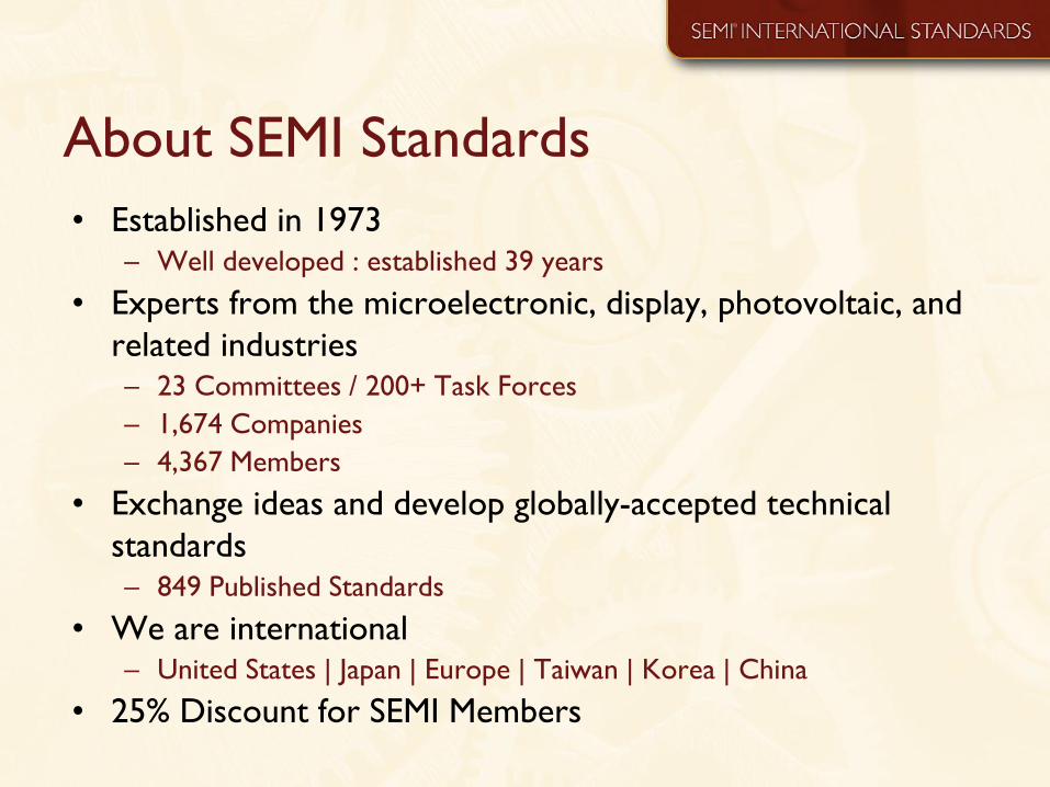
About SEMI Standards
• Established in 1973 – Well developed : established 39 years
• Experts from the microelectronic, display, photovoltaic, and
related industries – 23 Committees / 200+ Task Forces
– 1,674 Companies
– 4,367 Members
• Exchange ideas and develop globally-accepted technical
standards – 849 Published Standards
• We are international – United States | Japan | Europe | Taiwan | Korea | China
• 25% Discount for SEMI Members
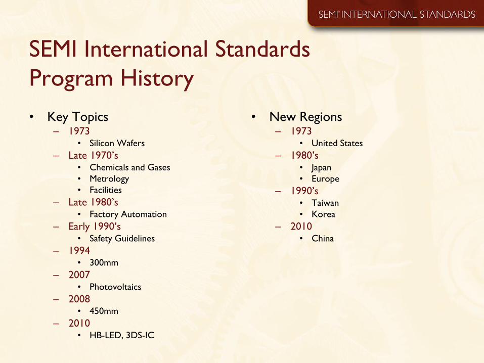
SEMI International Standards
Program History
• Key Topics – 1973
• Silicon Wafers
– Late 1970 s • Chemicals and Gases
• Metrology
• Facilities
– Late 1980 s • Factory Automation
– Early 1990 s • Safety Guidelines
– 1994 • 300mm
– 2007 • Photovoltaics
– 2008 • 450mm
– 2010 • HB-LED, 3DS-IC
• New Regions – 1973
• United States
– 1980 s • Japan
• Europe
– 1990 s • Taiwan
• Korea
– 2010 • China
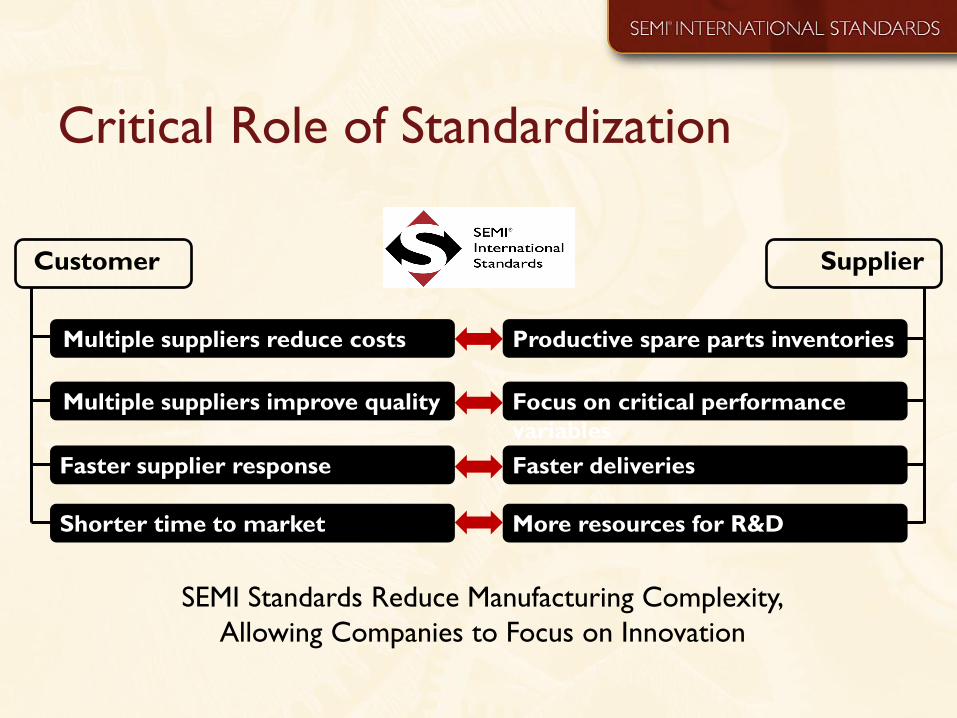
Critical Role of Standardization
Focus on critical performance
variables
More resources for R&D
Faster deliveries
Productive spare parts inventories Multiple suppliers reduce costs
Multiple suppliers improve quality
Faster supplier response
Shorter time to market
Customer Supplier
SEMI Standards Reduce Manufacturing Complexity,
Allowing Companies to Focus on Innovation
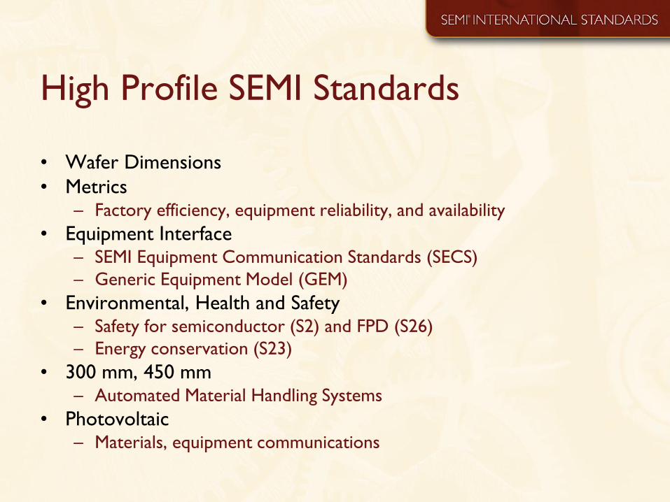
High Profile SEMI Standards
• Wafer Dimensions
• Metrics – Factory efficiency, equipment reliability, and availability
• Equipment Interface – SEMI Equipment Communication Standards (SECS)
– Generic Equipment Model (GEM)
• Environmental, Health and Safety – Safety for semiconductor (S2) and FPD (S26)
– Energy conservation (S23)
• 300 mm, 450 mm – Automated Material Handling Systems
• Photovoltaic – Materials, equipment communications
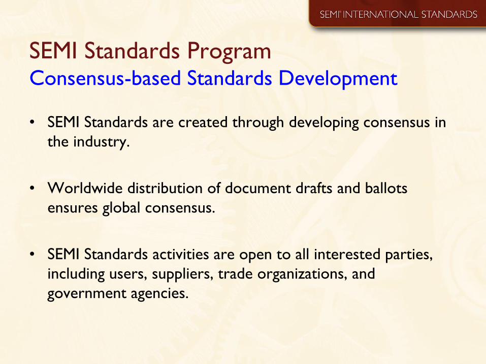
SEMI Standards Program Consensus-based Standards Development
• SEMI Standards are created through developing consensus in
the industry.
• Worldwide distribution of document drafts and ballots
ensures global consensus.
• SEMI Standards activities are open to all interested parties,
including users, suppliers, trade organizations, and
government agencies.
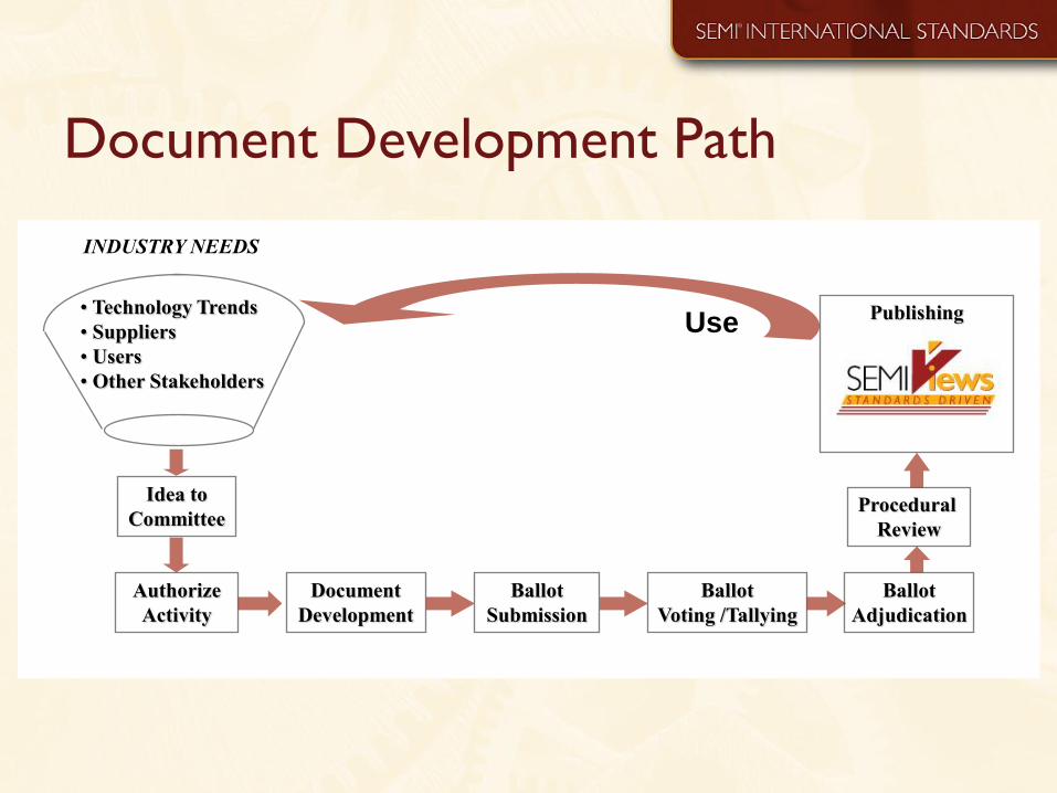
Document Development Path
• Technology Trends
• Suppliers
• Users
• Other Stakeholders
INDUSTRY NEEDS
Use
Authorize
Activity
Document
Development
Idea to
Committee
Ballot
Voting /Tallying
Publishing
Ballot
Adjudication
Procedural
Review
Ballot
Submission
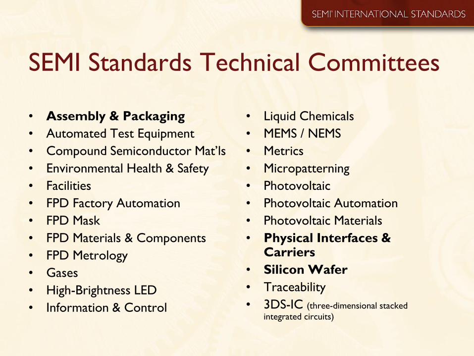
SEMI Standards Technical Committees
• Assembly & Packaging
• Automated Test Equipment
• Compound Semiconductor Mat’ls
• Environmental Health & Safety
• Facilities
• FPD Factory Automation
• FPD Mask
• FPD Materials & Components
• FPD Metrology
• Gases
• High-Brightness LED
• Information & Control
• Liquid Chemicals
• MEMS / NEMS
• Metrics
• Micropatterning
• Photovoltaic
• Photovoltaic Automation
• Photovoltaic Materials
• Physical Interfaces & Carriers
• Silicon Wafer
• Traceability
• 3DS-IC (three-dimensional stacked
integrated circuits)
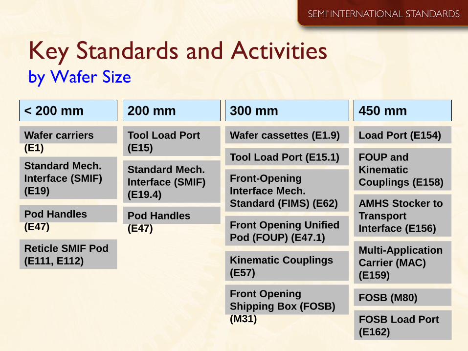
Key Standards and Activities by Wafer Size
< 200 mm
Wafer carriers
(E1)
200 mm 300 mm 450 mm
Standard Mech.
Interface (SMIF)
(E19)
Pod Handles
(E47)
Tool Load Port
(E15)
Standard Mech.
Interface (SMIF)
(E19.4)
Pod Handles
(E47)
Wafer cassettes (E1.9)
Tool Load Port (E15.1)
Front Opening Unified
Pod (FOUP) (E47.1)
Kinematic Couplings
(E57)
Front-Opening
Interface Mech.
Standard (FIMS) (E62)
Front Opening
Shipping Box (FOSB)
(M31)
Load Port (E154)
FOUP and
Kinematic
Couplings (E158)
AMHS Stocker to
Transport
Interface (E156)
Multi-Application
Carrier (MAC)
(E159)
Reticle SMIF Pod
(E111, E112)
FOSB (M80)
FOSB Load Port
(E162)
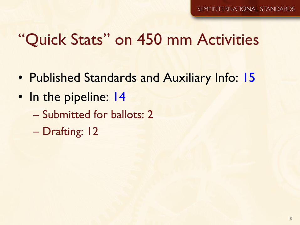
“Quick Stats” on 450 mm Activities
• Published Standards and Auxiliary Info: 15
• In the pipeline: 14
– Submitted for ballots: 2
– Drafting: 12
10
11
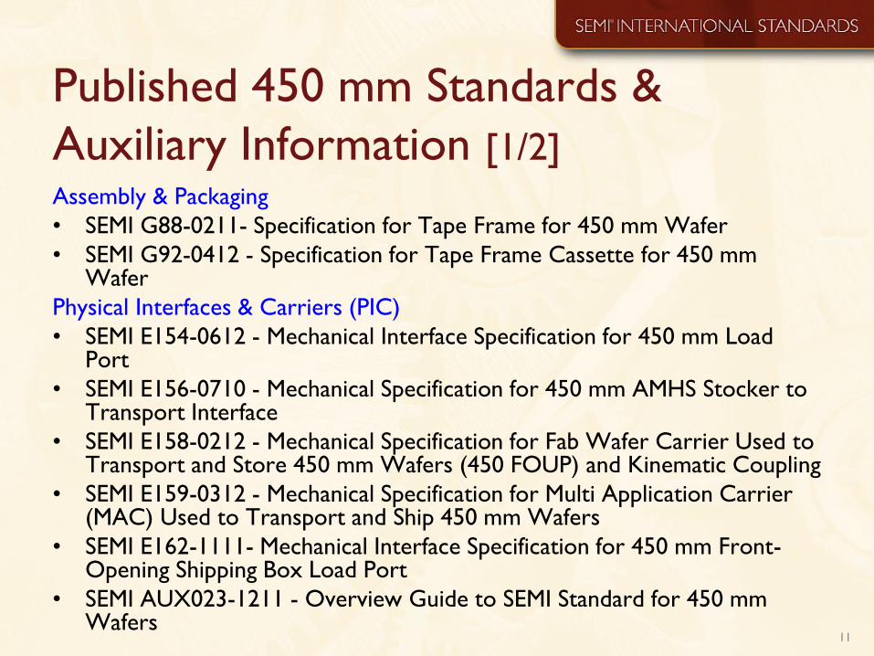
Published 450 mm Standards &
Auxiliary Information [1/2] Assembly & Packaging
• SEMI G88-0211- Specification for Tape Frame for 450 mm Wafer
• SEMI G92-0412 - Specification for Tape Frame Cassette for 450 mm Wafer
Physical Interfaces & Carriers (PIC)
• SEMI E154-0612 - Mechanical Interface Specification for 450 mm Load Port
• SEMI E156-0710 - Mechanical Specification for 450 mm AMHS Stocker to Transport Interface
• SEMI E158-0212 - Mechanical Specification for Fab Wafer Carrier Used to Transport and Store 450 mm Wafers (450 FOUP) and Kinematic Coupling
• SEMI E159-0312 - Mechanical Specification for Multi Application Carrier (MAC) Used to Transport and Ship 450 mm Wafers
• SEMI E162-1111- Mechanical Interface Specification for 450 mm Front-Opening Shipping Box Load Port
• SEMI AUX023-1211 - Overview Guide to SEMI Standard for 450 mm Wafers
12
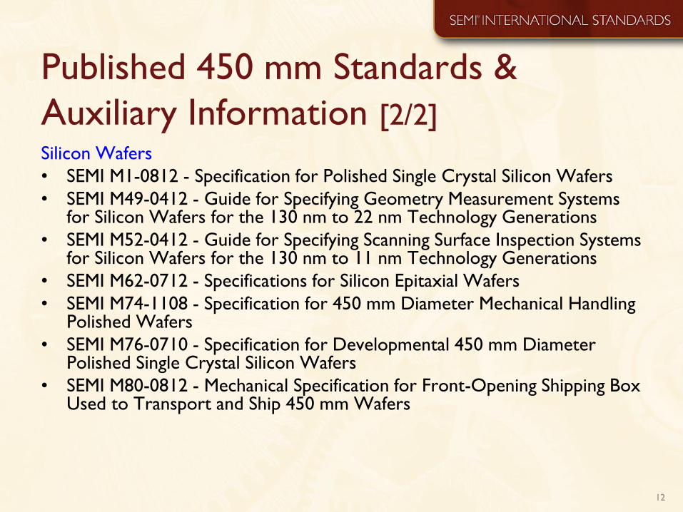
Published 450 mm Standards &
Auxiliary Information [2/2] Silicon Wafers
• SEMI M1-0812 - Specification for Polished Single Crystal Silicon Wafers
• SEMI M49-0412 - Guide for Specifying Geometry Measurement Systems for Silicon Wafers for the 130 nm to 22 nm Technology Generations
• SEMI M52-0412 - Guide for Specifying Scanning Surface Inspection Systems for Silicon Wafers for the 130 nm to 11 nm Technology Generations
• SEMI M62-0712 - Specifications for Silicon Epitaxial Wafers
• SEMI M74-1108 - Specification for 450 mm Diameter Mechanical Handling Polished Wafers
• SEMI M76-0710 - Specification for Developmental 450 mm Diameter Polished Single Crystal Silicon Wafers
• SEMI M80-0812 - Mechanical Specification for Front-Opening Shipping Box Used to Transport and Ship 450 mm Wafers
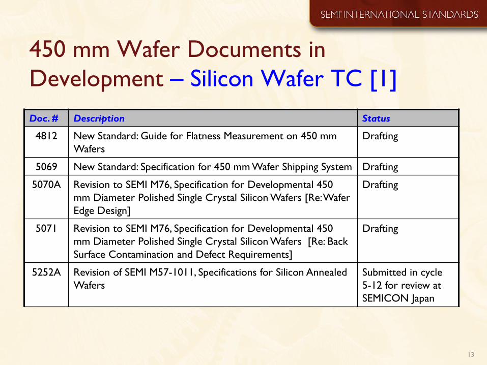
450 mm Wafer Documents in
Development – Silicon Wafer TC [1]
13
Doc. # Description Status
4812 New Standard: Guide for Flatness Measurement on 450 mm
Wafers
Drafting
5069 New Standard: Specification for 450 mm Wafer Shipping System Drafting
5070A Revision to SEMI M76, Specification for Developmental 450
mm Diameter Polished Single Crystal Silicon Wafers [Re: Wafer
Edge Design]
Drafting
5071 Revision to SEMI M76, Specification for Developmental 450
mm Diameter Polished Single Crystal Silicon Wafers [Re: Back
Surface Contamination and Defect Requirements]
Drafting
5252A Revision of SEMI M57-1011, Specifications for Silicon Annealed
Wafers
Submitted in cycle
5-12 for review at
SEMICON Japan
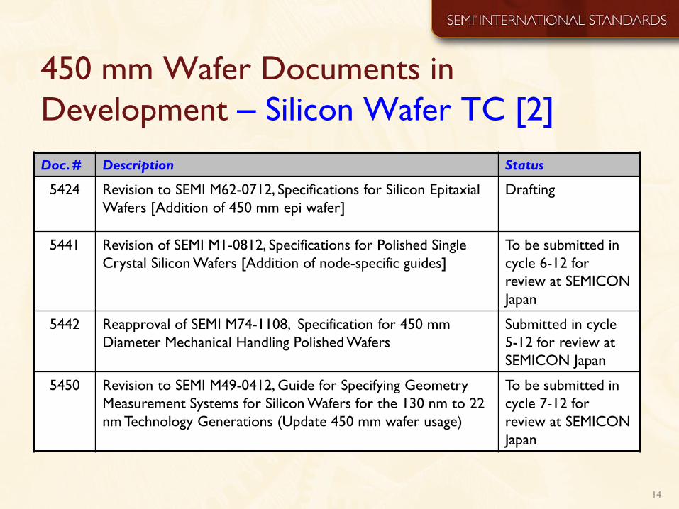
450 mm Wafer Documents in
Development – Silicon Wafer TC [2]
14
Doc. # Description Status
5424 Revision to SEMI M62-0712, Specifications for Silicon Epitaxial
Wafers [Addition of 450 mm epi wafer]
Drafting
5441 Revision of SEMI M1-0812, Specifications for Polished Single
Crystal Silicon Wafers [Addition of node-specific guides]
To be submitted in
cycle 6-12 for
review at SEMICON
Japan
5442 Reapproval of SEMI M74-1108, Specification for 450 mm
Diameter Mechanical Handling Polished Wafers
Submitted in cycle
5-12 for review at
SEMICON Japan
5450 Revision to SEMI M49-0412, Guide for Specifying Geometry
Measurement Systems for Silicon Wafers for the 130 nm to 22
nm Technology Generations (Update 450 mm wafer usage)
To be submitted in
cycle 7-12 for
review at SEMICON
Japan
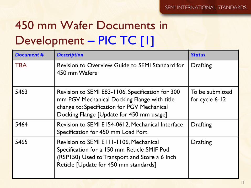
450 mm Wafer Documents in
Development – PIC TC [1]
15
Document # Description Status
TBA Revision to Overview Guide to SEMI Standard for
450 mm Wafers
Drafting
5463 Revision to SEMI E83-1106, Specification for 300
mm PGV Mechanical Docking Flange with title
change to: Specification for PGV Mechanical
Docking Flange [Update for 450 mm usage]
To be submitted
for cycle 6-12
5464 Revision to SEMI E154-0612, Mechanical Interface
Specification for 450 mm Load Port
Drafting
5465 Revision to SEMI E111-1106, Mechanical
Specification for a 150 mm Reticle SMIF Pod
(RSP150) Used to Transport and Store a 6 Inch
Reticle [Update for 450 mm standards]
Drafting
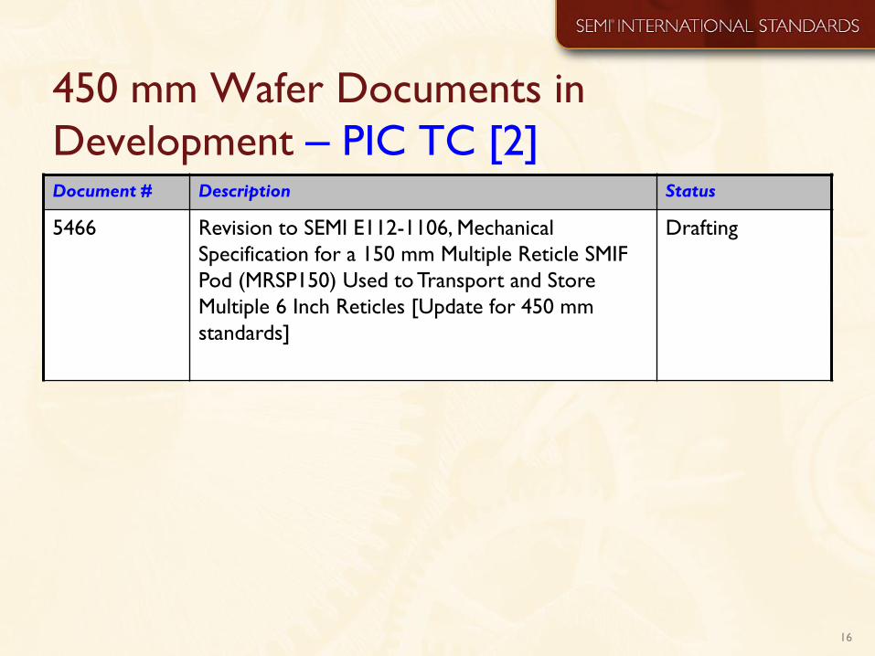
450 mm Wafer Documents in
Development – PIC TC [2]
16
Document # Description Status
5466 Revision to SEMI E112-1106, Mechanical
Specification for a 150 mm Multiple Reticle SMIF
Pod (MRSP150) Used to Transport and Store
Multiple 6 Inch Reticles [Update for 450 mm
standards]
Drafting
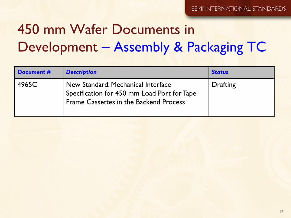
450 mm Wafer Documents in
Development – Assembly & Packaging TC
17
Document # Description Status
4965C New Standard: Mechanical Interface
Specification for 450 mm Load Port for Tape
Frame Cassettes in the Backend Process
Drafting
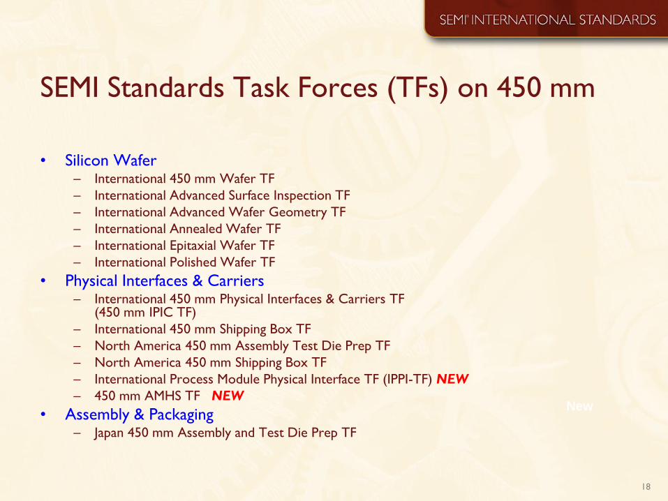
SEMI Standards Task Forces (TFs) on 450 mm
• Silicon Wafer – International 450 mm Wafer TF
– International Advanced Surface Inspection TF
– International Advanced Wafer Geometry TF
– International Annealed Wafer TF
– International Epitaxial Wafer TF
– International Polished Wafer TF
• Physical Interfaces & Carriers – International 450 mm Physical Interfaces & Carriers TF
(450 mm IPIC TF)
– International 450 mm Shipping Box TF
– North America 450 mm Assembly Test Die Prep TF
– North America 450 mm Shipping Box TF
– International Process Module Physical Interface TF (IPPI-TF) NEW
– 450 mm AMHS TF NEW
• Assembly & Packaging – Japan 450 mm Assembly and Test Die Prep TF
18
New
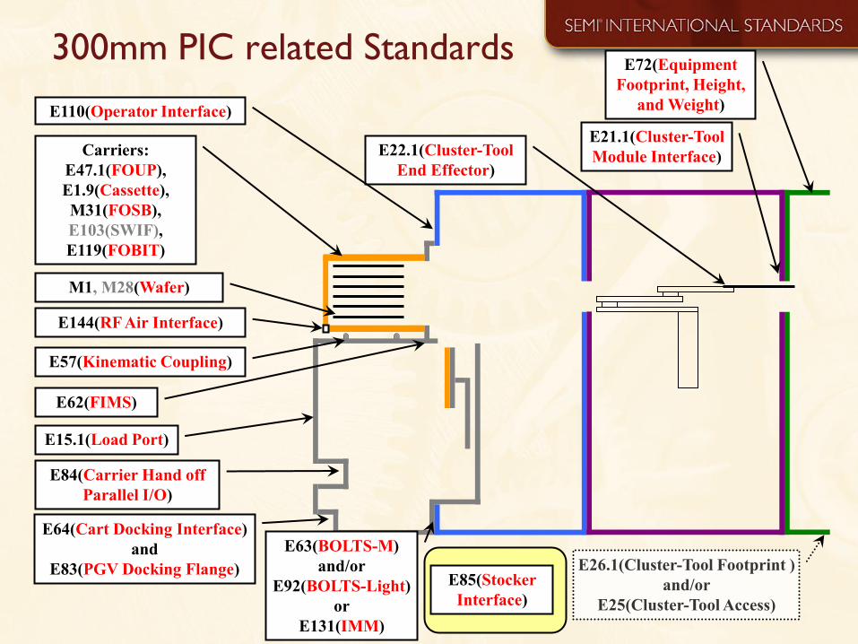
300mm PIC related Standards
E22.1(Cluster-Tool
End Effector)
E21.1(Cluster-Tool
Module Interface)
E72(Equipment
Footprint, Height,
and Weight)
Carriers:
E47.1(FOUP),
E1.9(Cassette),
M31(FOSB),
E103(SWIF),
E119(FOBIT)
M1, M28(Wafer)
E57(Kinematic Coupling)
E15.1(Load Port)
E62(FIMS)
E84(Carrier Hand off
Parallel I/O)
E64(Cart Docking Interface)
and
E83(PGV Docking Flange)
E63(BOLTS-M)
and/or
E92(BOLTS-Light)
or
E131(IMM)
E26.1(Cluster-Tool Footprint )
and/or
E25(Cluster-Tool Access)
E110(Operator Interface)
E144(RF Air Interface)
E85(Stocker
Interface)
Overview of 450mm SEMI Standards *Except packaging standards
Status
Carriers:
E158(450FOUP),
E159(450 MAC),
M80(450 FOSB)
E84(Carrier Hand off
Parallel I/O)
E144(RF Air Interface)
E154(FOUP & MAC
Load Port)
or
E162(FOSB Load Port)
Exx(PGV Docking Flange)
E156(Stocker
Interface)
E84(Carrier Hand off
Parallel I/O)
M74, M76, M1(Wafer)
Exx(Cluster-Tool
Module Interface)
Exx(Cluster-Tool
End Effector)
Published
Developing
No change Same as 300mm
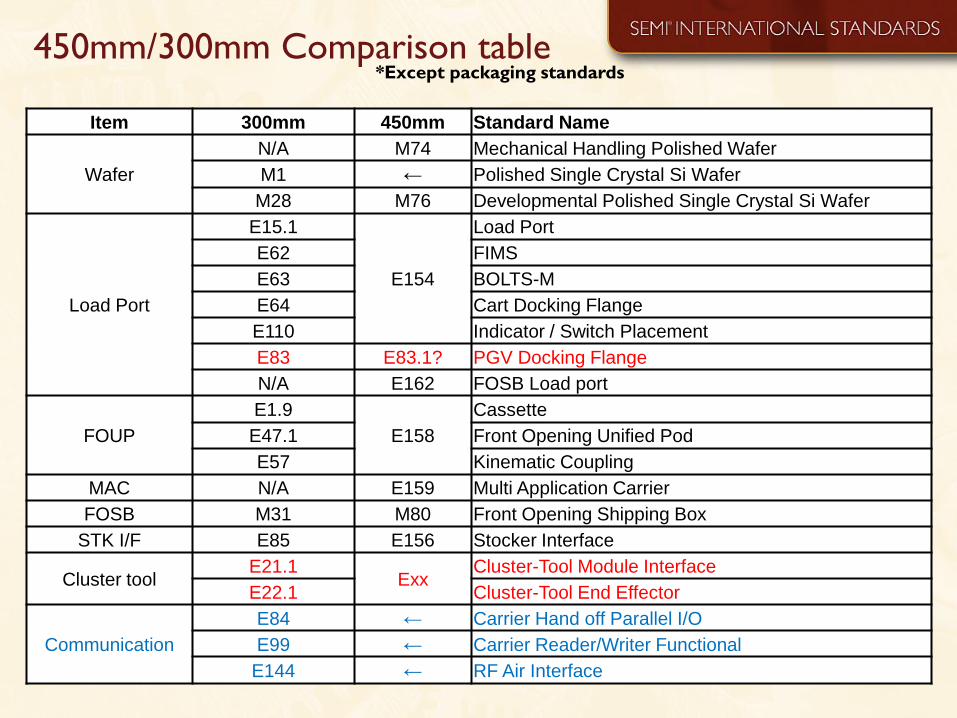
450mm/300mm Comparison table
Item 300mm 450mm Standard Name
Wafer
N/A M74 Mechanical Handling Polished Wafer
M1 ← Polished Single Crystal Si Wafer
M28 M76 Developmental Polished Single Crystal Si Wafer
Load Port
E15.1
E154
Load Port
E62 FIMS
E63 BOLTS-M
E64 Cart Docking Flange
E110 Indicator / Switch Placement
E83 E83.1? PGV Docking Flange
N/A E162 FOSB Load port
FOUP
E1.9
E158
Cassette
E47.1 Front Opening Unified Pod
E57 Kinematic Coupling
MAC N/A E159 Multi Application Carrier
FOSB M31 M80 Front Opening Shipping Box
STK I/F E85 E156 Stocker Interface
Cluster tool E21.1
Exx Cluster-Tool Module Interface
E22.1 Cluster-Tool End Effector
Communication
E84 ← Carrier Hand off Parallel I/O
E99 ← Carrier Reader/Writer Functional
E144 ← RF Air Interface
*Except packaging standards
Thank you!
• More information at:
www.semi.org/450
www.semi.org/standards


![Proposal for Adopting Thermoset Resin to Enable Joint ...semicontaiwan.org/zh/sites/semicontaiwan.org/files... · ] TCB epoxy flux Bump pitch [μm] 5x5 10x10 20x20 Reflowable epoxy](https://img.dokumen.tips/doc/110x75/5f3776570347d911a5200fe8/proposal-for-adopting-thermoset-resin-to-enable-joint-tcb-epoxy-flux-bump.jpg)