Embed Size (px)
Citation preview
SDI II MegaCore Function User Guide
101 Innovation DriveSan Jose, CA 95134www.altera.com
UG-011252013.06.28
Contents
SDI II MegaCore Function Quick Reference......................................................1-1
SDI II MegaCore Function Overview.................................................................2-1General Description.....................................................................................................................................2-1
SMPTE372 Dual Link Support.......................................................................................................2-2SMPTE RP168 Switching Support.................................................................................................2-4SD 20-Bits Interface for Dual/Triple Standard............................................................................2-4Tx PLL Dynamic Switching............................................................................................................2-5
Resource Utilization....................................................................................................................................2-7
Getting Started....................................................................................................3-1Installation and Licensing...........................................................................................................................3-1
OpenCore Plus Evaluation.............................................................................................................3-1OpenCore Plus Time-Out Behavior..............................................................................................3-2
Design Walkthrough...................................................................................................................................3-2Creating a New Quartus II Project................................................................................................3-2Launching MegaWizard Plug-In Manager...................................................................................3-3Parameterizing the MegaCore Function.......................................................................................3-3Generating a Design Example and Simulation Testbench.........................................................3-3Simulating the SDI II MegaCore Function Design.....................................................................3-4
Compiling the SDI II MegaCore Function Design.................................................................................3-5Programming an FPGA Device.................................................................................................................3-5Design Reference..........................................................................................................................................3-5
SDI II MegaCore Function Parameters........................................................................................3-6SDI II MegaCore Function Component Files..............................................................................3-8Video Pattern Generator Signals...................................................................................................3-8Transceiver Reconfiguration Controller Signals.........................................................................3-9Reconfiguration Router Signals...................................................................................................3-10Design Examples............................................................................................................................3-10
Functional Description.......................................................................................4-1Protocol.........................................................................................................................................................4-1
Altera Corporation
SDI II MegaCore Function User GuideTOC-2
Transmitter.......................................................................................................................................4-2Receiver.............................................................................................................................................4-4
Transceiver....................................................................................................................................................4-8Submodules...................................................................................................................................................4-9
Insert Line.......................................................................................................................................4-10Insert/Check CRC..........................................................................................................................4-10Insert VPID.....................................................................................................................................4-11Match TRS......................................................................................................................................4-12Scrambler........................................................................................................................................4-13Tx Sample........................................................................................................................................4-13Clock Enable Generator................................................................................................................4-13Rx Sample........................................................................................................................................4-14Detect Video Standard..................................................................................................................4-15Detect 1 and 1/1.001 Rates............................................................................................................4-16Transceiver Controller..................................................................................................................4-16Descrambler....................................................................................................................................4-17TRS Aligner.....................................................................................................................................4-173Gb Demux.....................................................................................................................................4-18Extract Line.....................................................................................................................................4-18Extract VPID..................................................................................................................................4-19Detect Format.................................................................................................................................4-19Sync Streams...................................................................................................................................4-20Convert SD Bits..............................................................................................................................4-20
Clocking Scheme........................................................................................................................................4-20SDI II MegaCore Function Signals..........................................................................................................4-20
Additional Information......................................................................................5-1Document Revision History.......................................................................................................................5-1How to Contact Altera................................................................................................................................5-2
Altera Corporation
TOC-3SDI II MegaCore Function User Guide
1SDI II MegaCore Function Quick Reference
2013.06.28
UG-01125 Subscribe Feedback
The Altera®
Serial Digital Interface (SDI) II MegaCore®
function is the next generation SDI intellectualproperty (IP).
The SDI II MegaCore function is part of the MegaCore IP Library, which is distributed with the Quartus®
II software and downloadable from the Altera website at www.altera.com.
For system requirements and installation instructions, refer toAltera Software Installation&Licensing.Note:
Table 1-1: Brief Information About the SDI II MegaCore Function
DescriptionItem
13.0SP1Version
ReleaseInformation
July 2013Release Date
IP-SDI-IIOrdering Code
0111Product ID(s)
6AF7Vendor ID
• 270-Mbps SD-SDI, as defined by SMPTE259M specification• 1.485-Gbps or 1.4835-Gbps HD-SDI, as defined by SMPTE292M
specification• 2.97-Gbps or 2.967-Gbps 3G-SDI, as defined by SMPTE424M
specification• Dual link HD-SDI, as defined by SMPTE372M specification• Dual standard support for SD-SDI and HD-SDI• Triple standard support for SD-SDI, HD-SDI, and 3G-SDI• 20-bit interface support for SD-SDI• SMPTE425M level A support (direct source image formatting)• SMPTE425M level B support (dual link mapping)• SMPTE RP168 switching support
SDI Data Rate SupportIP CoreInformation
ISO9001:2008Registered
© 2013 Altera Corporation. All rights reserved. ALTERA, ARRIA, CYCLONE, HARDCOPY, MAX, MEGACORE, NIOS, QUARTUS and STRATIXwords and logos are trademarks of Altera Corporation and registered in the U.S. Patent and Trademark Office and in other countries. All other wordsand logos identified as trademarks or service marks are the property of their respective holders as described at www.altera.com/common/legal.html.Altera warrants performance of its semiconductor products to current specifications in accordance with Altera's standard warranty, but reserves theright to make changes to any products and services at any time without notice. Altera assumes no responsibility or liability arising out of the applicationor use of any information, product, or service described herein except as expressly agreed to in writing by Altera. Altera customers are advised toobtain the latest version of device specifications before relying on any published information and before placing orders for products or services.
www.altera.com
101 Innovation Drive, San Jose, CA 95134
DescriptionItem
• Multiple SDI standards and video formats• Videopayload identification (VPID)packet insertion and extraction• Clock enable generator• Video rate detection• Cyclical redundancy check (CRC) encoding and decoding (HD
only)• Line number (LN) insertion and extraction (HD only)• Word scrambling and descrambling• Word alignment• Transmitter clock multiplexer (optional)• Framing and extraction of video timing signals• Dual link data stream synchronization (HD only)• IPUTF compliance core (hw.tcl)• IEEE encryption for functional simulation• Transceiver dynamic reconfiguration• Dynamic generation of simulation testbench• Dynamic generation of design example entity• RP168 support for synchronous video switching• Tx PLL dynamic switching• OpenCore Plus evaluation
Features
IP CoreInformation
• Digital video equipment• Mixing and recording equipment
Application
Arria®
V, Cyclone®
V, and Stratix®
V FPGA device families.
Refer to the device support table andWhat’s New in Altera IP page ofthe Altera website for detailed information.
Device Family Support
• MegaWizard™ Plug-In Manager in the Quartus II software fordesign creation and compilation
• ModelSim®-Altera, Riviera-Pro, and VCS/VCS MX software for
design simulation or synthesis
Design Tools
Related Information
• Altera Software Installation and Licensing
• Device Family Support
• What's New in Altera IP
SDI II MegaCore Function Quick ReferenceAltera Corporation
Feedback
UG-01125SDI II MegaCore Function Quick Reference1-2 2013.06.28
2SDI II MegaCore Function Overview
2013.06.28
UG-01125 Subscribe Feedback
The SDI II MegaCore function implements a transmitter, receiver, or full-duplex SDI at standard definition(SD), high definition (HD), or 3 gigabits per second (3G) rate as defined by the Society of Motion Pictureand Television Engineers (SMPTE). The SDI II MegaCore function supports dual standard (SD-SDI andHD-SDI) and triple standard (SD-SDI, HD-SDI, and 3G-SDI). These modes provide automatic receiver ratedetection and transceiver dynamic reconfiguration.
The SDI II MegaCore function highlights the following new features:
• Supports 28 nm devices and beyond.
• Arria V and Stratix V from Quartus II version 12.1 onwards• Arria V GZ and Cyclone V from Quartus II version 13.0 onwards
• IPUTF compliance core (hw.tcl).• IEEE encryption for functional simulation.• Dynamic generation of user simulation testbench that matches the IP configuration.• Dynamic generation of design example that serves as common entity for simulation and hardware
verification.
General DescriptionThe SMPTE defines a SDI standard that is widely used as an interconnect between equipment in videoproduction facilities. The SDI II MegaCore function can handle the following SDI data rates:
• 270megabits per second (Mbps) SD-SDI, as defined by SMPTE259M-1997 10-Bit 4:2:2 Component SerialDigital Interface
• 1.485 gigabits per second (Gbps) or 1.4835-Gbps HD-SDI, as defined by SMPTE292M-1998 Bit-SerialDigital Interface for High Definition Television Systems
• 2.97-Gbps or 2.967-Gbps 3G SDI, as defined by SMPTE424M• Dual link HD-SDI, as defined by SMPTE372M-Dual Link 1.5Gb/s Digital Interface for 1920×1080 and
2048×1080 Picture Formats• Dual standard support for SD-SDI and HD-SDI• Triple standard support for SD-SDI, HD-SDI, and 3G-SDI• SMPTE425M level A support (direct source image formatting)• SMPTE425M level B support (dual link mapping)• SMPTE RP168 switching support
ISO9001:2008Registered
© 2013 Altera Corporation. All rights reserved. ALTERA, ARRIA, CYCLONE, HARDCOPY, MAX, MEGACORE, NIOS, QUARTUS and STRATIXwords and logos are trademarks of Altera Corporation and registered in the U.S. Patent and Trademark Office and in other countries. All other wordsand logos identified as trademarks or service marks are the property of their respective holders as described at www.altera.com/common/legal.html.Altera warrants performance of its semiconductor products to current specifications in accordance with Altera's standard warranty, but reserves theright to make changes to any products and services at any time without notice. Altera assumes no responsibility or liability arising out of the applicationor use of any information, product, or service described herein except as expressly agreed to in writing by Altera. Altera customers are advised toobtain the latest version of device specifications before relying on any published information and before placing orders for products or services.
www.altera.com
101 Innovation Drive, San Jose, CA 95134
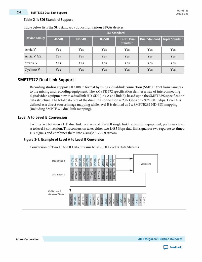
Table 2-1: SDI Standard Support
Table below lists the SDI standard support for various FPGA devices.SDI Standard
Device Family Triple StandardDual StandardHD-SDI DualStandard
3G-SDIHD-SDISD-SDI
YesYesYesYesYesYesArria V
YesYesYesYesYesYesArria V GZ
YesYesYesYesYesYesStratix V
YesYesYesYesYesYesCyclone V
SMPTE372 Dual Link SupportRecording studios support HD 1080p format by using a dual-link connection (SMPTE372) from camerasto the mixing and recording equipment. The SMPTE 372 specification defines a way of interconnectingdigital video equipmentwith a dual linkHD-SDI (linkA and link B), based upon the SMPTE292 specificationdata structure. The total data rate of the dual link connection is 2.97 Gbps or 2.97/1.001 Gbps. Level A isdefined as a direct source image mapping while level B is defined as 2 x SMPTE292 HD-SDI mapping(including SMPTE372 dual link mapping).
Level A to Level B Conversion
To interface between a HD dual link receiver and 3G-SDI single link transmitter equipment, perform a levelA to level B conversion. This conversion takes either two 1.485Gbps dual link signals or two separate co-timedHD signals and combines them into a single 3G-SDI stream.
Figure 2-1: Example of Level A to Level B Conversion
Conversion of Two HD-SDI Data Streams to 3G-SDI Level B Data Streams
3FFh(C1)
3FFh(Y1)
000h(C1)
000h(Y1)
XYZ(C1
)XY
Z(Y1
)LN
0(C1
)LN
0(Y1
)LN
1(C1
)LN
1(Y1
)
3FFh(C2)
3FFh(Y2)
000h(C2)
000h(Y2)
XYZ(C2
)XY
Z(Y2
)LN
0(C2
)LN
0(Y2
)LN
1(C2
)LN
1(Y2
)
000h(C1)
000h(Y1)
000h(C2)
000h(Y2)
MultiplexingData Stream 1
Data Stream 2
3G-SDI Level BInterleaved Stream
3FFh(C2)
3FFh(C1)
3FFh(Y2)
3FFh(Y1)
000h(C2)
000h(C1)
000h(Y2)
000h(Y1)
XYZ(C2
)XY
Z(C1
)XY
Z(Y2
)XY
Z(Y1
)LN
0(C2
)LN
0(C1
)LN
0(Y2
)LN
0(Y1
)LN
1(C2
)LN
1(C1
)LN
1(Y2
)LN
1(Y1
)
SDI II MegaCore Function OverviewAltera Corporation
Feedback
UG-01125SMPTE372 Dual Link Support2-2 2013.06.28
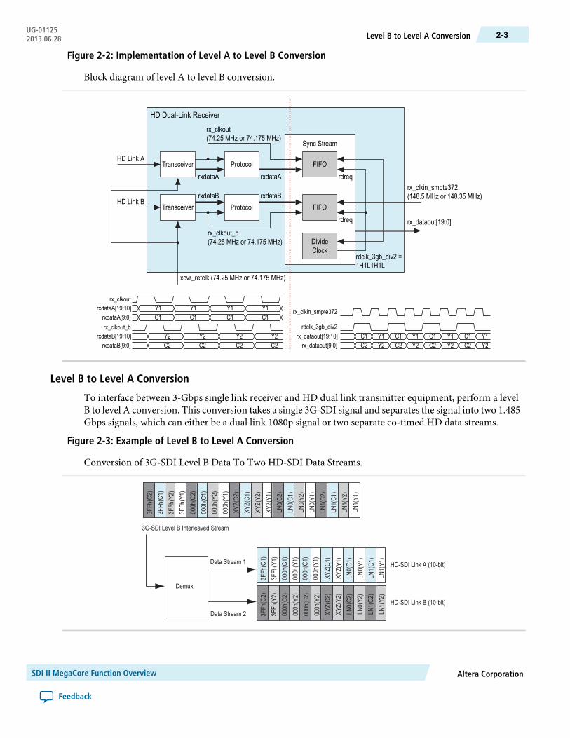
Figure 2-2: Implementation of Level A to Level B Conversion
Block diagram of level A to level B conversion.
TransceiverHD Link A
Protocol FIFOrxdataA rxdataA rdreq
TransceiverHD Link B
Protocol FIFOrxdataB rxdataB
rdreq
DivideClock
rx_clkin_smpte372(148.5 MHz or 148.35 MHz)
rx_dataout[19:0]
rdclk_3gb_div2 =1H1L1H1L
xcvr_refclk (74.25 MHz or 74.175 MHz)
rx_clkout(74.25 MHz or 74.175 MHz)
rx_clkout_b(74.25 MHz or 74.175 MHz)
Sync Stream
HD Dual-Link Receiver
Y1 Y1 Y1 Y1C1 C1 C1 C1
Y2 Y2 Y2 Y2C2 C2 C2 C2
rx_clkoutrxdataA[19:10]rxdataA[9:0]rx_clkout_b
rxdataB[19:10]rxdataB[9:0]
rx_clkin_smpte372
rdclk_3gb_div2rx_dataout[19:10]rx_dataout[9:0]
C1 C1 C1 C1Y1 Y1 Y1 Y1C2 C2 C2 C2Y2 Y2 Y2 Y2
Level B to Level A Conversion
To interface between 3-Gbps single link receiver and HD dual link transmitter equipment, perform a levelB to level A conversion. This conversion takes a single 3G-SDI signal and separates the signal into two 1.485Gbps signals, which can either be a dual link 1080p signal or two separate co-timed HD data streams.
Figure 2-3: Example of Level B to Level A Conversion
Conversion of 3G-SDI Level B Data To Two HD-SDI Data Streams.
3FFh(C2)
Demux
3FFh(C1)
3FFh(Y2)
3FFh(Y1)
000h(C2)
000h(C1)
000h(Y2)
000h(Y1)
XYZ(C2
)XY
Z(C1
)XY
Z(Y2
)XY
Z(Y1
)LN
0(C2
)LN
0(C1
)LN
0(Y2
)LN
0(Y1
)LN
1(C2
)LN
1(C1
)LN
1(Y2
)LN
1(Y1
)
3FFh(C1)
3FFh(Y1)
000h(C1)
000h(Y1)
XYZ(C1
)XY
Z(Y1
)LN
0(C1
)LN
0(Y1
)LN
1(C1
)LN
1(Y1
)
3FFh(C2)
3FFh(Y2)
000h(C2)
000h(Y2)
XYZ(C2
)XY
Z(Y2
)LN
0(C2
)LN
0(Y2
)LN
1(C2
)LN
1(Y2
)
000h(C1)
000h(Y1)
000h(C2)
000h(Y2)
3G-SDI Level B Interleaved Stream
Data Stream 1 HD-SDI Link A (10-bit)
HD-SDI Link B (10-bit)Data Stream 2
Altera CorporationSDI II MegaCore Function Overview
Feedback
2-3Level B to Level A ConversionUG-011252013.06.28
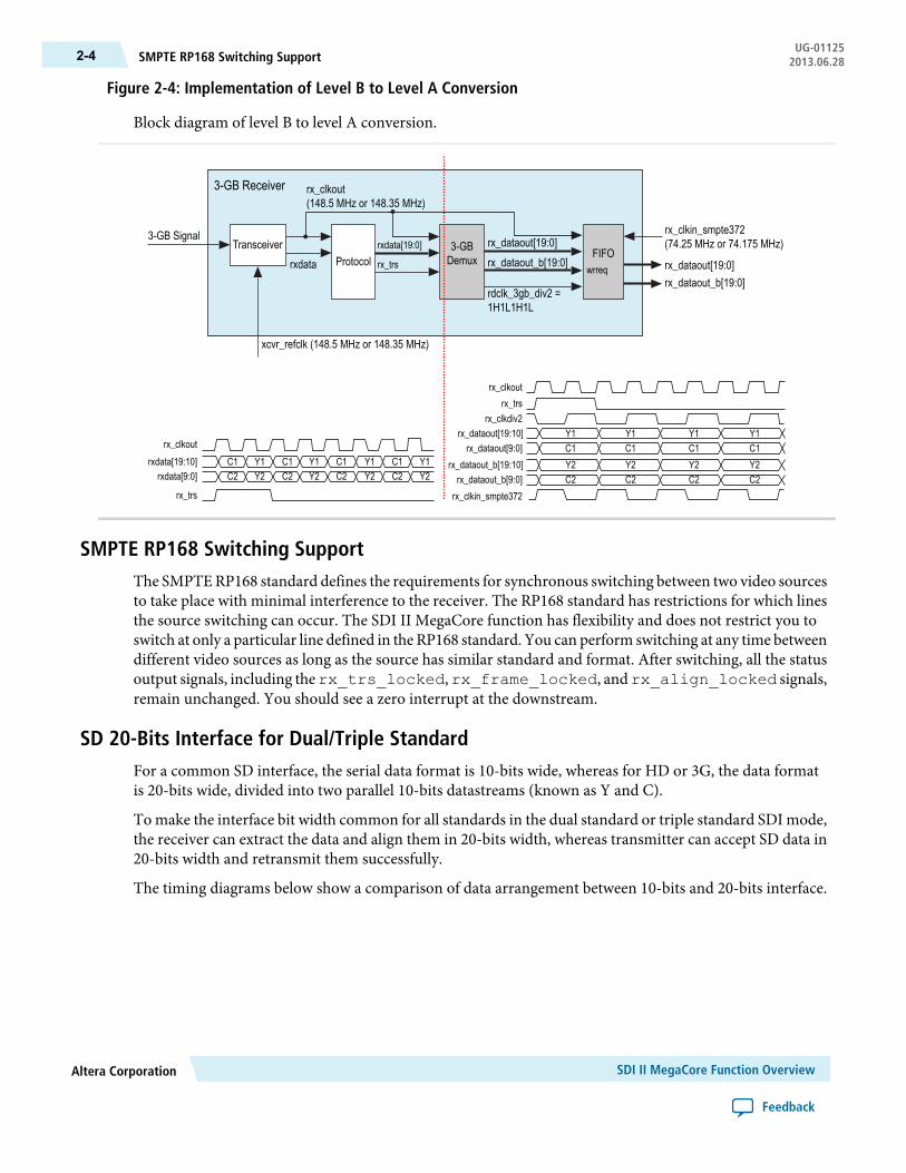
Figure 2-4: Implementation of Level B to Level A Conversion
Block diagram of level B to level A conversion.
Transceiver3-GB Signal
Protocol3-GBDemuxrxdata
rx_clkin_smpte372(74.25 MHz or 74.175 MHz)
rx_dataout[19:0]
rdclk_3gb_div2 =1H1L1H1L
xcvr_refclk (148.5 MHz or 148.35 MHz)
rx_clkout(148.5 MHz or 148.35 MHz)
FIFO
rx_dataout_b[19:0]
rx_dataout[19:0]rx_dataout_b[19:0] wrreq
rxdata[19:0]
rx_trs
3-GB Receiver
rx_clkout
rx_trs
rxdata[19:10]rxdata[9:0]
C1 C1 C1 C1Y1 Y1 Y1 Y1C2 C2 C2 C2Y2 Y2 Y2 Y2
Y1 Y1 Y1 Y1C1 C1 C1 C1Y2 Y2 Y2 Y2C2 C2 C2 C2
rx_clkin_smpte372
rx_dataout[19:10]rx_dataout[9:0]
rx_clkdiv2
rx_dataout_b[19:10]rx_dataout_b[9:0]
rx_clkoutrx_trs
SMPTE RP168 Switching SupportThe SMPTERP168 standard defines the requirements for synchronous switching between two video sourcesto take place with minimal interference to the receiver. The RP168 standard has restrictions for which linesthe source switching can occur. The SDI II MegaCore function has flexibility and does not restrict you toswitch at only a particular line defined in the RP168 standard. You can perform switching at any time betweendifferent video sources as long as the source has similar standard and format. After switching, all the statusoutput signals, including therx_trs_locked,rx_frame_locked, andrx_align_locked signals,remain unchanged. You should see a zero interrupt at the downstream.
SD 20-Bits Interface for Dual/Triple StandardFor a common SD interface, the serial data format is 10-bits wide, whereas for HD or 3G, the data formatis 20-bits wide, divided into two parallel 10-bits datastreams (known as Y and C).
To make the interface bit width common for all standards in the dual standard or triple standard SDI mode,the receiver can extract the data and align them in 20-bits width, whereas transmitter can accept SD data in20-bits width and retransmit them successfully.
The timing diagrams below show a comparison of data arrangement between 10-bits and 20-bits interface.
SDI II MegaCore Function OverviewAltera Corporation
Feedback
UG-01125SMPTE RP168 Switching Support2-4 2013.06.28
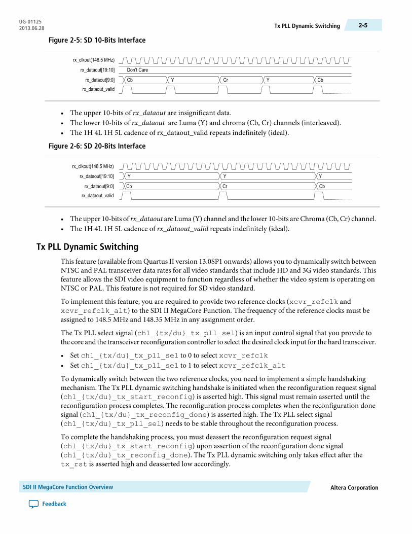
Figure 2-5: SD 10-Bits Interface
rx_clkout(148.5 MHz)
rx_dataout[19:10]
rx_dataout[9:0]rx_dataout_valid
Don’t Care
Cb Y Cr Y Cb
• The upper 10-bits of rx_dataout are insignificant data.• The lower 10-bits of rx_dataout are Luma (Y) and chroma (Cb, Cr) channels (interleaved).• The 1H 4L 1H 5L cadence of rx_dataout_valid repeats indefinitely (ideal).
Figure 2-6: SD 20-Bits Interface
rx_clkout(148.5 MHz)
rx_dataout[19:10]
rx_dataout[9:0]rx_dataout_valid
Cb
Y
Cr
Y Y
Cb
• The upper 10-bits of rx_dataout are Luma (Y) channel and the lower 10-bits are Chroma (Cb, Cr) channel.• The 1H 4L 1H 5L cadence of rx_dataout_valid repeats indefinitely (ideal).
Tx PLL Dynamic SwitchingThis feature (available from Quartus II version 13.0SP1 onwards) allows you to dynamically switch betweenNTSC and PAL transceiver data rates for all video standards that include HD and 3G video standards. Thisfeature allows the SDI video equipment to function regardless of whether the video system is operating onNTSC or PAL. This feature is not required for SD video standard.
To implement this feature, you are required to provide two reference clocks (xcvr_refclk andxcvr_refclk_alt) to the SDI II MegaCore Function. The frequency of the reference clocks must beassigned to 148.5 MHz and 148.35 MHz in any assignment order.
The Tx PLL select signal (ch1_{tx/du}_tx_pll_sel) is an input control signal that you provide tothe core and the transceiver reconfiguration controller to select the desired clock input for the hard transceiver.
• Set ch1_{tx/du}_tx_pll_sel to 0 to select xcvr_refclk• Set ch1_{tx/du}_tx_pll_sel to 1 to select xcvr_refclk_alt
To dynamically switch between the two reference clocks, you need to implement a simple handshakingmechanism. The Tx PLL dynamic switching handshake is initiated when the reconfiguration request signal(ch1_{tx/du}_tx_start_reconfig) is asserted high. This signal must remain asserted until thereconfiguration process completes. The reconfiguration process completes when the reconfiguration donesignal (ch1_{tx/du}_tx_reconfig_done) is asserted high. The Tx PLL select signal(ch1_{tx/du}_tx_pll_sel) needs to be stable throughout the reconfiguration process.
To complete the handshaking process, you must deassert the reconfiguration request signal(ch1_{tx/du}_tx_start_reconfig) upon assertion of the reconfiguration done signal(ch1_{tx/du}_tx_reconfig_done). The Tx PLL dynamic switching only takes effect after thetx_rst is asserted high and deasserted low accordingly.
Altera CorporationSDI II MegaCore Function Overview
Feedback
2-5Tx PLL Dynamic SwitchingUG-011252013.06.28
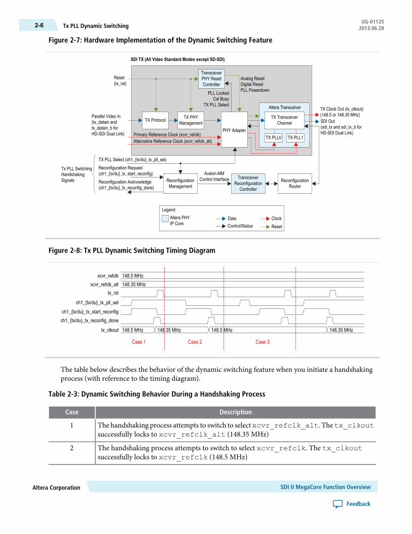
Figure 2-7: Hardware Implementation of the Dynamic Switching Feature
TX Protocol TX PHYManagement
PHY Adapter
TransceiverPHY ResetController
TransceiverReconfiguration
Controller
ReconfigurationManagement
ReconfigurationRouter
TX TransceiverChannel
TX PLL0 TX PLL1
Parallel Video In(tx_datain andtx_datain_b forHD-SDI Dual Link) Primary Reference Clock (xcvr_refclk)
Alternative Reference Clock (xcvr_refclk_alt)
Reset(tx_rst)
Tx PLL SwitchingHandshakingSignals Reconfiguration Acknowledge
(ch1_{tx/du}_tx_reconfig_done)
Reconfiguration Request(ch1_{tx/du}_tx_start_reconfig)
TX PLL Select (ch1_{tx/du}_tx_pll_sel)
Avalon-MMControl Interface
TX Clock Out (tx_clkout)(148.5 or 148.35 MHz)SDI Out(sdi_tx and sdi_tx_b forHD-SDI Dual Link)
Altera Transceiver
Analog ResetDigital ResetPLL PowerdownPLL Locked
Cal BusyTX PLL Select
SDI TX (All Video Standard Modes except SD-SDI)
Altera PHYIP Core
DataControl/Status
ClockReset
Legend
Figure 2-8: Tx PLL Dynamic Switching Timing Diagram
148.5 MHz148.35 MHz
148.5 MHz
Case 1 Case 2 Case 3
148.35 MHz 148.5 MHz 148.35 MHz
xcvr_refclkxcvr_refclk_alt
tx_rst
ch1_{tx/du}_tx_pll_selch1_{tx/du}_tx_start_reconfigch1_{tx/du}_tx_reconfig_done
tx_clkout
The table below describes the behavior of the dynamic switching feature when you initiate a handshakingprocess (with reference to the timing diagram).
Table 2-3: Dynamic Switching Behavior During a Handshaking Process
DescriptionCase
The handshaking process attempts to switch to selectxcvr_refclk_alt. Thetx_clkoutsuccessfully locks to xcvr_refclk_alt (148.35 MHz)
1
The handshaking process attempts to switch to select xcvr_refclk. The tx_clkoutsuccessfully locks to xcvr_refclk (148.5 MHz)
2
SDI II MegaCore Function OverviewAltera Corporation
Feedback
UG-01125Tx PLL Dynamic Switching2-6 2013.06.28
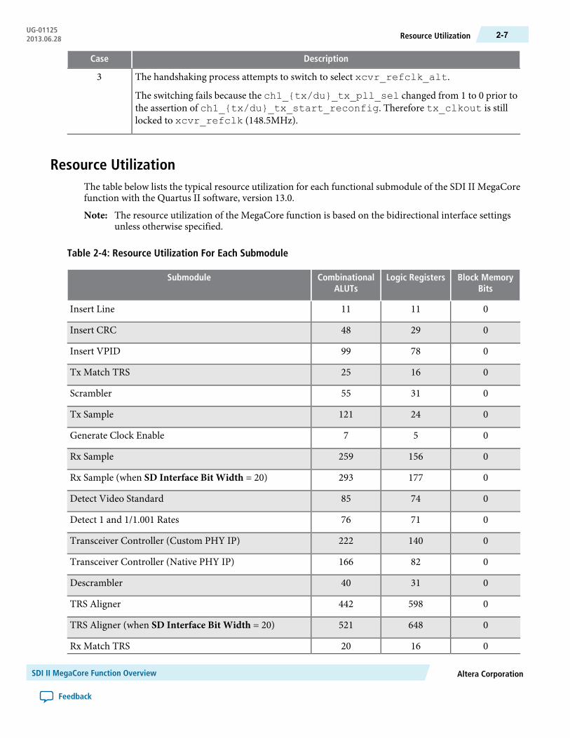
DescriptionCase
The handshaking process attempts to switch to select xcvr_refclk_alt.
The switching fails because the ch1_{tx/du}_tx_pll_sel changed from 1 to 0 prior tothe assertion of ch1_{tx/du}_tx_start_reconfig. Therefore tx_clkout is stilllocked to xcvr_refclk (148.5MHz).
3
Resource UtilizationThe table below lists the typical resource utilization for each functional submodule of the SDI II MegaCorefunction with the Quartus II software, version 13.0.
The resource utilization of the MegaCore function is based on the bidirectional interface settingsunless otherwise specified.
Note:
Table 2-4: Resource Utilization For Each Submodule
Block MemoryBits
Logic RegistersCombinationalALUTs
Submodule
01111Insert Line
02948Insert CRC
07899Insert VPID
01625Tx Match TRS
03155Scrambler
024121Tx Sample
057Generate Clock Enable
0156259Rx Sample
0177293Rx Sample (when SD Interface Bit Width = 20)
07485Detect Video Standard
07176Detect 1 and 1/1.001 Rates
0140222Transceiver Controller (Custom PHY IP)
082166Transceiver Controller (Native PHY IP)
03140Descrambler
0598442TRS Aligner
0648521TRS Aligner (when SD Interface Bit Width = 20)
01620Rx Match TRS
Altera CorporationSDI II MegaCore Function Overview
Feedback
2-7Resource UtilizationUG-011252013.06.28
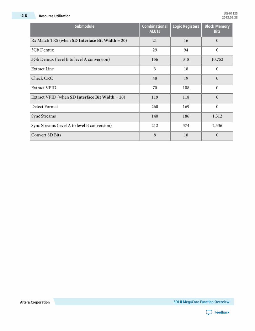
Block MemoryBits
Logic RegistersCombinationalALUTs
Submodule
01621Rx Match TRS (when SD Interface Bit Width = 20)
094293Gb Demux
10,7523181563Gb Demux (level B to level A conversion)
0183Extract Line
01948Check CRC
010870Extract VPID
0118119Extract VPID (when SD Interface Bit Width = 20)
0169260Detect Format
1,312186140Sync Streams
2,336374212Sync Streams (level A to level B conversion)
0188Convert SD Bits
SDI II MegaCore Function OverviewAltera Corporation
Feedback
UG-01125Resource Utilization2-8 2013.06.28
3Getting Started
2013.06.28
UG-01125 Subscribe Feedback
Installation and LicensingTo evaluate the SDI IIMegaCore function using theOpenCore Plus feature, follow these steps in your designflow:
1. Install the SDI II MegaCore function.2. Create a custom variation of the SDI II MegaCore function.3. Implement the rest of your design using the design entry method of your choice.4. Use the IP functional simulation model to verify the operation of your design.5. Compile your design in the Quartus II software. You can also generate an OpenCore Plus time-limited
programming file, which you can use to verify the operation of your design in hardware.
For more information on IP functional simulation models, refer to the Simulating Altera Designschapter in volume 3 of the Quartus II Handbook.
Note:
The default installation directory for the SDI II MegaCore function on Windows is c:\altera\<version>; onLinux, it is /opt/ altera<version>.
You can obtain a license for the MegaCore function only when you are completely satisfied with itsfunctionality and performance, and want to take your design to production. After you purchase a licensefor the SDI II MegaCore function, follow these steps:
1. Set up licensing.2. Generate a programming file for the Altera device or devices on your board.3. Program the Altera device or devices with the completed design.
Related InformationSimulating Altera Designs
OpenCore Plus EvaluationTheAlteraOpenCore evaluation feature allows you to generate RTL files and simulationmodels to simulate,compile, and validate timing.However, youmust acquire a license to generate a programming file to configurean FPGA. Without a license for the variation in your design, you cannot create an SRAM Object File (.sof)or a Programmer Object File (.pof) for programming a device with your design.
ISO9001:2008Registered
© 2013 Altera Corporation. All rights reserved. ALTERA, ARRIA, CYCLONE, HARDCOPY, MAX, MEGACORE, NIOS, QUARTUS and STRATIXwords and logos are trademarks of Altera Corporation and registered in the U.S. Patent and Trademark Office and in other countries. All other wordsand logos identified as trademarks or service marks are the property of their respective holders as described at www.altera.com/common/legal.html.Altera warrants performance of its semiconductor products to current specifications in accordance with Altera's standard warranty, but reserves theright to make changes to any products and services at any time without notice. Altera assumes no responsibility or liability arising out of the applicationor use of any information, product, or service described herein except as expressly agreed to in writing by Altera. Altera customers are advised toobtain the latest version of device specifications before relying on any published information and before placing orders for products or services.
www.altera.com
101 Innovation Drive, San Jose, CA 95134
With the free OpenCore Plus evaluation feature, you can perform the following actions:
• Simulate the behavior of a megafunction (Altera MegaCore function or AMPPSM megafunction) withinyour system.
• Verify the design functionality and quickly evaluate its size and speed.• Generate time-limited device programming files for designs that include MegaCore functions.• Program a device and verify your design in hardware.
OpenCore Plus Time-Out BehaviorThe OpenCore Plus evaluation can support the following modes of operation:
• Untethered—the design runs for a limited time.• Tethered—requires a connection between your board and the host computer. If all megafunctions in a
design supports the tethered mode, the device can operate for a longer time or indefinitely.
All megafunctions in a device time out simultaneously when reaching the most restrictive evaluation time.If there is more than one megafunction in a design, a specific megafunction’s time-out behavior might bemasked by the time-out behavior of the other megafunctions.
For MegaCore functions, the untethered time-out is 1 hour; the tethered time-out value is indefinite.Note:
Your design stops working after the hardware evaluation time expires and the rst signal goes high.
Related Information
• Altera Software Installation and Licensing
• AN 320: OpenCorePlus Evaluation of Megafunctions
Design WalkthroughThis walkthrough explains how to create an SDI IIMegaCore function design using theMegaWizard Plug-InManager and theQuartus II software. After you generate a custom variation of the SDI IIMegaCore function,you can incorporate it into your overall project.
This walkthrough includes the following steps:
1. Creating a New Quartus II Project on page 3-22. Launching MegaWizard Plug-In Manager on page 3-33. Parameterizing the MegaCore Function on page 3-34. Generating a Design Example and Simulation Testbench on page 3-35. Simulating the SDI II MegaCore Function Design on page 3-4
Creating a New Quartus II ProjectYou need to create a new Quartus II project with the New Project Wizard, which specifies the workingdirectory for the project, assigns the project name, and designates the name of the top-level design entity.
To create a new project, perform the following the steps.
1. From the Windows Start menu, select Programs > Altera > Quartus II <version> to run the Quartus IIsoftware. Alternatively, you can use the Quartus II Web Edition software.
Getting StartedAltera Corporation
Feedback
UG-01125OpenCore Plus Time-Out Behavior3-2 2013.06.28
2. On the File menu, click New Project Wizard.3. In the New Project Wizard: Directory, Name, Top-Level Entity page, specify the working directory,
project name, and top-level design entity name. Click Next.4. In the New Project Wizard: Add Files page, select the existing design files (if any) you want to include
in the project.2 Click Next.5. In the New Project Wizard: Family & Device Settings page, select the device family and specific device
you want to target for compilation. Click Next.6. In the EDA Tool Settings page, select the EDA tools you want to use with the Quartus II software to
develop your project.7. The last page in the New Project Wizard window shows the summary of your chosen settings. Click
Finish to complete the Quartus II project creation.
Launching MegaWizard Plug-In ManagerTo launch the MegaWizard Plug-In Manager in the Quartus II software, follow these steps:
1. On the Tools menu, click MegaWizard Plug-In Manager.2. Select Create a new custom megafunction variation and click Next.3. Select your target device family from the list.4. Expand the Interfaces > SDI folder and click SDI II <version>.5. Select the output file type for your design; the wizard supports VHDL and Verilog HDL.6. Affix a variation name for the MegaCore function output files <project path>\<variation name>. The
MegaWizard Plug-In Manager shows the project path that you specified in the New Project Wizard.7. Click Next to display the SDI II MegaCore function parameter editor.
Parameterizing the MegaCore FunctionTo parameterize your MegaCore function, follow these steps:
1. Select the video standard.2. Select Bidirectional, Transmitter, or Receiver interface direction.3. Select Combined, Transceiver, or Protocol.4. Turn on the necessary transceiver options. Some options are grayed out if it is not supported in a selected
configuration.5. Turn on the necessary receiver options.6. Turn on the necessary transmitter options.7. Click Finish.
Related InformationSDI II MegaCore Function Parameters on page 3-6
Generating a Design Example and Simulation TestbenchAfter you have parameterized the MegaCore function, you have the option to generate a design example, inaddition to generating the MegaCore component files.
2 To include existing files, you must specify the directory path to where you installed the SDI II MegaCorefunction. You must also add the user libraries if you installed the MegaCore IP Library in a different directoryfrom where you installed the Quartus II software.
Altera CorporationGetting Started
Feedback
3-3Launching MegaWizard Plug-In ManagerUG-011252013.06.28
To generate a design example, check the Generate Example Design option to create the following entities:
• design example— serves as a common entity for simulation and hardware verification.• simulation testbench—consists of the design example entity and other non-synthesizable components.
The example testbench and the automated script are located in the<variation name>_example/sdi_ii/simulation/verilog or<variation name>_example/sdi_ii/simulation/vhdl directory.
Generating a design example can increase processing time.Note:
You can now integrate your custom MegaCore function variation into your design, simulate, and compile.
Simulating the SDI II MegaCore Function DesignAfter design generation, the files located in the <variation name>_example/sdi_ii/simulation/verilog or<variation name>_example/sdi_ii/simulation/vhdl directory are available for you to simulate your design.
The SDI II MegaCore function supports the following EDA simulators listed in the table below.
Table 3-2: Supported EDA Simulators
Supported LanguageSupported PlatformSimulator
VHDL and Verilog HDLWindows/LinuxModelSim-Altera SE/AE
VerilogWindows/LinuxVCS/VCS MX
VerilogLinuxAldec Riviera-PRO
To simulate the design using the ModelSim®-Altera simulator, follow these steps:
1. Start the ModelSim-Altera simulator.2. On the File menu, click Change Directory > Select
<variation name>_example_design/sdi_ii/simulation/verilog (for Verilog HDL language) or_example_design/sdi_ii/simulation/vhdl (for VHDL language).
3. On the File menu, click Load >Macro file. Select run_sim.tcl. This file compiles the design and runs thesimulation automatically, providing a pass/fail indication on completion.
To simulate the design using the VCS/VCS MX simulator (in Linux), follow these steps:
1. Start the VCS/VCS MX simulator.2. On the File menu, click Change Directory > Select
<variation name>_example_design/sdi_ii/simulation/verilog.3. Run source run_vcs.sh (for VCS) or source run_vcsmx.sh (for VCSMX). This file compiles the design
and runs the simulation automatically, providing a pass/fail indication on completion.
To simulate the design using the Aldec Riviera-PRO simulator, follow these steps:
1. Start the Aldec Riviera-PRO simulator.2. On the File menu, click Change Directory > Select
<variation name>_example_design/sdi_ii/simulation/verilog.3. On the Tools menu, click Execute Macro. Select run_riviera.tcl. This file compiles the design and runs
the simulation automatically, providing a pass/fail indication on completion.
Getting StartedAltera Corporation
Feedback
UG-01125Simulating the SDI II MegaCore Function Design3-4 2013.06.28
Compiling the SDI II MegaCore Function DesignTo compile your design, click Start Compilation on the Processing menu in the Quartus II software. Youcan use the generated .qip file to include relevant files into your project.
You can find the design examples of the SDI II MegaCore function in the<variation name>_example_design/sdi_ii/example_design/sdi_ii_0001_example_design directory. Forthe design example illustrations, refer to the Design Examples section.
To create a new project using the generated design example, follow the steps in the Creating a NewQuartus II Project section and add the design example .qip file in step 4.
Note:
Related Information
• Quartus II HelpMore information about compilation in Quartus II software.
• Creating a New Quartus II Project on page 3-2
• Design Examples on page 3-10
Programming an FPGA DeviceAfter successfully compiling your design, program the targetedAltera devicewith theQuartus II Programmerand verify the design in hardware.
For instructions on programming the FPGA device, refer to the Device Programming section in volume 3of the Quartus II Handbook.
Related InformationDevice Programming
Design ReferenceThis section describes the SDI II MegaCore function parameters, signals, and files to help you configureyour design. This section includes detailed description about the SDI II MegaCore function design examples.
Altera CorporationGetting Started
Feedback
3-5Compiling the SDI II MegaCore Function DesignUG-011252013.06.28
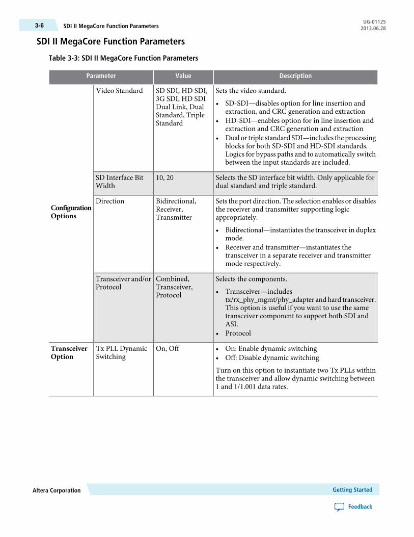
SDI II MegaCore Function Parameters
Table 3-3: SDI II MegaCore Function Parameters
DescriptionValueParameter
Sets the video standard.
• SD-SDI—disables option for line insertion andextraction, and CRC generation and extraction
• HD-SDI—enables option for in line insertion andextraction and CRC generation and extraction
• Dual or triple standard SDI—includes the processingblocks for both SD-SDI and HD-SDI standards.Logics for bypass paths and to automatically switchbetween the input standards are included.
SD SDI, HD SDI,3G SDI, HD SDIDual Link, DualStandard, TripleStandard
Video Standard
ConfigurationOptions
Selects the SD interface bit width. Only applicable fordual standard and triple standard.
10, 20SD Interface BitWidth
Sets the port direction. The selection enables or disablesthe receiver and transmitter supporting logicappropriately.
• Bidirectional—instantiates the transceiver in duplexmode.
• Receiver and transmitter—instantiates thetransceiver in a separate receiver and transmittermode respectively.
Bidirectional,Receiver,Transmitter
Direction
Selects the components.
• Transceiver—includestx/rx_phy_mgmt/phy_adapter andhard transceiver.This option is useful if you want to use the sametransceiver component to support both SDI andASI.
• Protocol
Combined,Transceiver,Protocol
Transceiver and/orProtocol
• On: Enable dynamic switching• Off: Disable dynamic switching
Turn on this option to instantiate two Tx PLLs withinthe transceiver and allow dynamic switching between1 and 1/1.001 data rates.
On, OffTx PLL DynamicSwitching
TransceiverOption
Getting StartedAltera Corporation
Feedback
UG-01125SDI II MegaCore Function Parameters3-6 2013.06.28
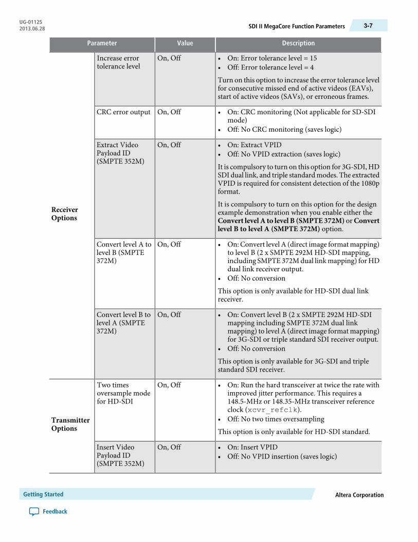
DescriptionValueParameter
• On: Error tolerance level = 15• Off: Error tolerance level = 4
Turn on this option to increase the error tolerance levelfor consecutive missed end of active videos (EAVs),start of active videos (SAVs), or erroneous frames.
On, OffIncrease errortolerance level
ReceiverOptions
• On: CRC monitoring (Not applicable for SD-SDImode)
• Off: No CRC monitoring (saves logic)
On, OffCRC error output
• On: Extract VPID• Off: No VPID extraction (saves logic)
It is compulsory to turn on this option for 3G-SDI, HDSDI dual link, and triple standardmodes. The extractedVPID is required for consistent detection of the 1080pformat.
It is compulsory to turn on this option for the designexample demonstration when you enable either theConvert level A to level B (SMPTE372M) orConvertlevel B to level A (SMPTE 372M) option.
On, OffExtract VideoPayload ID(SMPTE 352M)
• On:Convert level A (direct image formatmapping)to level B (2 x SMPTE 292M HD-SDI mapping,including SMPTE 372Mdual linkmapping) forHDdual link receiver output.
• Off: No conversion
This option is only available for HD-SDI dual linkreceiver.
On, OffConvert level A tolevel B (SMPTE372M)
• On: Convert level B (2 x SMPTE 292M HD-SDImapping including SMPTE 372M dual linkmapping) to level A (direct image formatmapping)for 3G-SDI or triple standard SDI receiver output.
• Off: No conversion
This option is only available for 3G-SDI and triplestandard SDI receiver.
On, OffConvert level B tolevel A (SMPTE372M)
• On: Run the hard transceiver at twice the rate withimproved jitter performance. This requires a148.5-MHz or 148.35-MHz transceiver referenceclock (xcvr_refclk).
• Off: No two times oversampling
This option is only available for HD-SDI standard.
On, OffTwo timesoversample modefor HD-SDI
TransmitterOptions
• On: Insert VPID• Off: No VPID insertion (saves logic)
On, OffInsert VideoPayload ID(SMPTE 352M)
Altera CorporationGetting Started
Feedback
3-7SDI II MegaCore Function ParametersUG-011252013.06.28
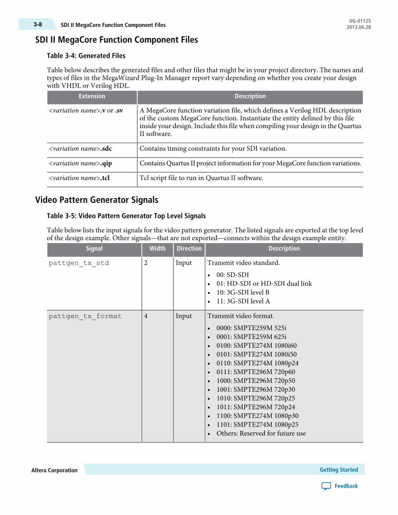
SDI II MegaCore Function Component Files
Table 3-4: Generated Files
Table below describes the generated files and other files that might be in your project directory. The names andtypes of files in the MegaWizard Plug-In Manager report vary depending on whether you create your designwith VHDL or Verilog HDL.
DescriptionExtension
A MegaCore function variation file, which defines a Verilog HDL descriptionof the custom MegaCore function. Instantiate the entity defined by this fileinside your design. Include this file when compiling your design in theQuartusII software.
<variation name>.v or .sv
Contains timing constraints for your SDI variation.<variation name>.sdc
ContainsQuartus II project information for yourMegaCore function variations.<variation name>.qip
Tcl script file to run in Quartus II software.<variation name>.tcl
Video Pattern Generator Signals
Table 3-5: Video Pattern Generator Top Level Signals
Table below lists the input signals for the video pattern generator. The listed signals are exported at the top levelof the design example. Other signals—that are not exported—connects within the design example entity.
DescriptionDirectionWidthSignal
Transmit video standard.
• 00: SD-SDI• 01: HD-SDI or HD-SDI dual link• 10: 3G-SDI level B• 11: 3G-SDI level A
Input2pattgen_tx_std
Transmit video format.
• 0000: SMPTE259M 525i• 0001: SMPTE259M 625i• 0100: SMPTE274M 1080i60• 0101: SMPTE274M 1080i50• 0110: SMPTE274M 1080p24• 0111: SMPTE296M 720p60• 1000: SMPTE296M 720p50• 1001: SMPTE296M 720p30• 1010: SMPTE296M 720p25• 1011: SMPTE296M 720p24• 1100: SMPTE274M 1080p30• 1101: SMPTE274M 1080p25• Others: Reserved for future use
Input4pattgen_tx_format
Getting StartedAltera Corporation
Feedback
UG-01125SDI II MegaCore Function Component Files3-8 2013.06.28
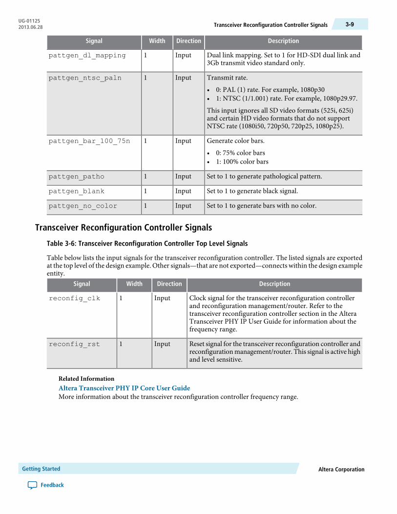
DescriptionDirectionWidthSignal
Dual link mapping. Set to 1 for HD-SDI dual link and3Gb transmit video standard only.
Input1pattgen_dl_mapping
Transmit rate.
• 0: PAL (1) rate. For example, 1080p30• 1: NTSC (1/1.001) rate. For example, 1080p29.97.
This input ignores all SD video formats (525i, 625i)and certain HD video formats that do not supportNTSC rate (1080i50, 720p50, 720p25, 1080p25).
Input1pattgen_ntsc_paln
Generate color bars.
• 0: 75% color bars• 1: 100% color bars
Input1pattgen_bar_100_75n
Set to 1 to generate pathological pattern.Input1pattgen_patho
Set to 1 to generate black signal.Input1pattgen_blank
Set to 1 to generate bars with no color.Input1pattgen_no_color
Transceiver Reconfiguration Controller Signals
Table 3-6: Transceiver Reconfiguration Controller Top Level Signals
Table below lists the input signals for the transceiver reconfiguration controller. The listed signals are exportedat the top level of the design example. Other signals—that are not exported—connects within the design exampleentity.
DescriptionDirectionWidthSignal
Clock signal for the transceiver reconfiguration controllerand reconfiguration management/router. Refer to thetransceiver reconfiguration controller section in the AlteraTransceiver PHY IP User Guide for information about thefrequency range.
Input1reconfig_clk
Reset signal for the transceiver reconfiguration controller andreconfigurationmanagement/router. This signal is active highand level sensitive.
Input1reconfig_rst
Related InformationAltera Transceiver PHY IP Core User GuideMore information about the transceiver reconfiguration controller frequency range.
Altera CorporationGetting Started
Feedback
3-9Transceiver Reconfiguration Controller SignalsUG-011252013.06.28
Reconfiguration Router Signals
Table 3-7: Reconfiguration Router Top Level Signals
Table below lists the signals for the reconfiguration router. The listed signals are exported at the top level of thedesign example. Other signals—that are not exported—connects within the design example entity.
DescriptionDirec-tion
WidthSignal
Dynamic reconfiguration request signal forTx PLL dynamic switching at transmitter orduplex instance at channel 1.
This signal is only available if you turn on theTx PLL Dynamic Switching option.
Refer to the Tx PLL Dynamic Switching forthe usage requirement.
Input1ch1_<direction>_tx_start_reconfig
Tx PLL select signal for Tx PLL dynamicswitching at transmitter or duplex instance atchannel 1. This signal is also connected toxcvr_refclk_sel signal of the SDI instance.
This signal is only available if you turn on theTx PLL Dynamic Switching option.
Refer to the Tx PLL Dynamic Switching forthe usage requirement.
Input1ch1_<direction>_tx_pll_sel
Dynamic reconfiguration acknowledge signalfor Tx PLL dynamic switching at transmitteror duplex instance at channel 1.
This signal is only available if you turn on theTx PLL Dynamic Switching option.
Output1ch1_<direction>_tx_reconfig_done
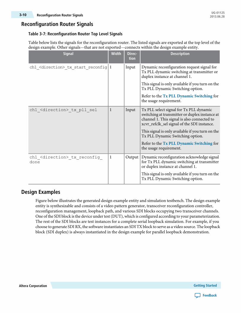
Design ExamplesFigure below illustrates the generated design example entity and simulation testbench. The design exampleentity is synthesizable and consists of a video pattern generator, transceiver reconfiguration controller,reconfiguration management, loopback path, and various SDI blocks occupying two transceiver channels.One of the SDI block is the device under test (DUT), which is configured according to your parameterization.The rest of the SDI blocks are test instances for a complete serial loopback simulation. For example, if youchoose to generate SDI RX, the software instantiates an SDI TX block to serve as a video source. The loopbackblock (SDI duplex) is always instantiated in the design example for parallel loopback demonstration.
Getting StartedAltera Corporation
Feedback
UG-01125Reconfiguration Router Signals3-10 2013.06.28
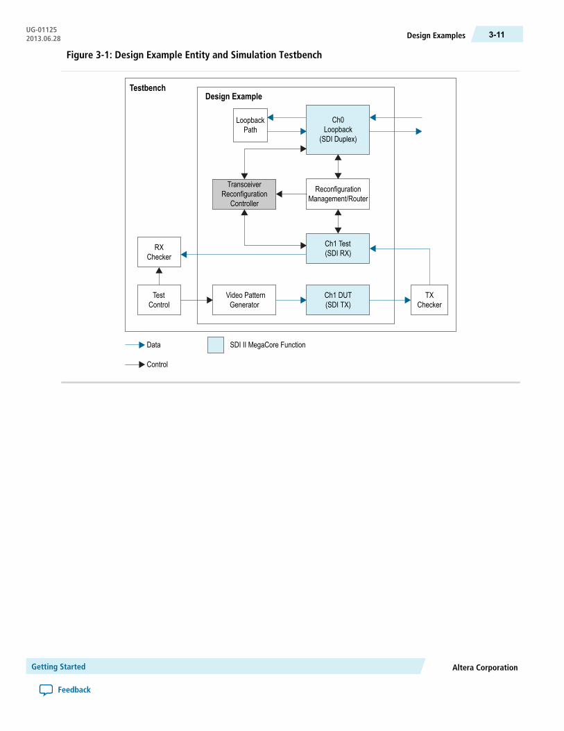
Figure 3-1: Design Example Entity and Simulation Testbench
LoopbackPath
Ch0Loopback
(SDI Duplex)
ReconfigurationManagement/Router
Ch1 Test(SDI RX)
Ch1 DUT(SDI TX)
TransceiverReconfiguration
Controller
Video PatternGenerator
TXChecker
RXChecker
TestControl
Data
Control
SDI II MegaCore Function
Design ExampleTestbench
Altera CorporationGetting Started
Feedback
3-11Design ExamplesUG-011252013.06.28
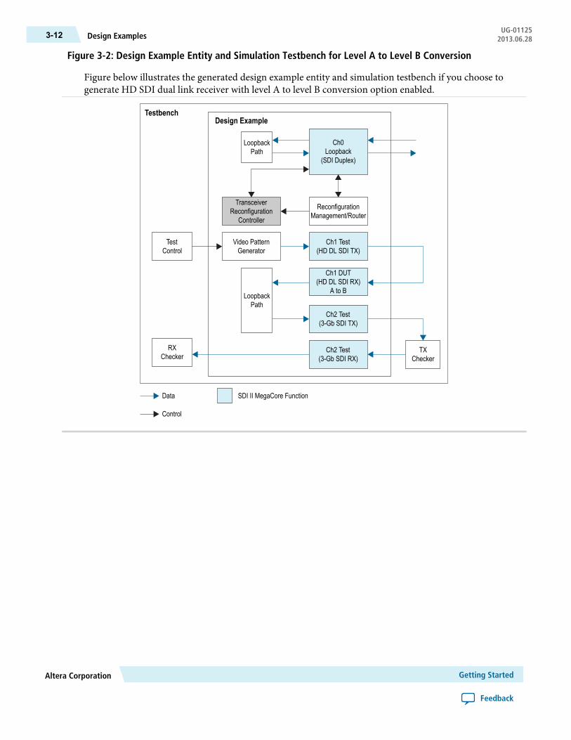
Figure 3-2: Design Example Entity and Simulation Testbench for Level A to Level B Conversion
Figure below illustrates the generated design example entity and simulation testbench if you choose togenerate HD SDI dual link receiver with level A to level B conversion option enabled.
LoopbackPath
Ch0Loopback
(SDI Duplex)
ReconfigurationManagement/Router
Ch1 Test(HD DL SDI TX)
Ch1 DUT(HD DL SDI RX)
A to B
Video PatternGenerator
TestControl
Ch2 Test(3-Gb SDI TX)
Ch2 Test(3-Gb SDI RX)
TXChecker
RXChecker
LoopbackPath
Data
Control
SDI II MegaCore Function
Design ExampleTestbench
TransceiverReconfiguration
Controller
Getting StartedAltera Corporation
Feedback
UG-01125Design Examples3-12 2013.06.28
Figure 3-3: Design Example Entity and Simulation Testbench for Level B to Level A Conversion
Figure below illustrates the generated design example entity and simulation testbench when you choose togenerate 3G SDI or triple rate SDI receiver with level B to level A conversion option enabled.
LoopbackPath
Ch0Loopback
(SDI Duplex)
ReconfigurationManagement/Router
Ch1 Test(3-Gb SDI TX)
Ch1 DUT(3-Gb SDI RX)
B to A
Video PatternGenerator
TestControl
Ch2 Test(HD DL SDI TX)
Ch2 Test(HD DL SDI RX)
TXChecker
RXChecker
LoopbackPath
Data
Control
SDI II MegaCore Function
Design ExampleTestbench
TransceiverReconfiguration
Controller
Design Example Components
The design examples for the SDI II MegaCore function consist of the following components:
• Video pattern generator• Transceiver reconfiguration controller• Reconfiguration management• Reconfiguration router
Video Pattern Generator
The video pattern generator generates a colorbar or pathological pattern. The colorbar is preferable for imagegeneration while the pathological pattern can stress the PLL and cable equalizer of the attached videoequipment. You can configure the video pattern generator to generate various video formats.
Altera CorporationGetting Started
Feedback
3-13Design Example ComponentsUG-011252013.06.28
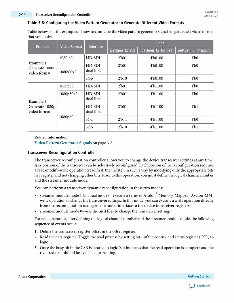
Table 3-8: Configuring the Video Pattern Generator to Generate Different Video Formats
Table below lists the examples of how to configure the video pattern generator signals to generate a video formatthat you desire.
SignalInterfaceVideo FormatExample
pattgen_dl_mappingpattgen_tx_formatpattgen_tx_std
1'b04'b01002'b01HD-SDI1080i60Example 1:Generate 1080ivideo format
1'b04'b01002'b01HD-SDIdual link1080i60x2
1'b04'b01002'b103Gb
1'b04'b11002'b01HD-SDI1080p30
Example 2:Generate 1080pvideo format
1'b04'b11002'b01HD-SDIdual link
1080p30x2
1'b14'b11002'b01HD-SDIdual link
1080p60 1'b04'b11002'b113Ga
1'b14'b11002'b103Gb
Related InformationVideo Pattern Generator Signals on page 3-8
Transceiver Reconfiguration Controller
The transceiver reconfiguration controller allows you to change the device transceiver settings at any time.Any portion of the transceiver can be selectively reconfigured. Each portion of the reconfiguration requiresa read-modify-write operation (read first, then write), in such a way by modifying only the appropriate bitsin a register and not changing other bits. Prior to this operation, you must define the logical channel numberand the streamer module mode.
You can perform a transceiver dynamic reconfiguration in these two modes:
• streamer module mode 1 (manual mode)—execute a series of Avalon®Memory-Mapped (Avalon-MM)write operation to change the transceiver settings. In this mode, you can execute a write operation directlyfrom the reconfiguration management/router interface to the device transceiver registers.
• streamer module mode 0—use the .mif files to change the transceiver settings.
For read operation, after defining the logical channel number and the streamer module mode, the followingsequence of events occur:
1. Define the transceiver register offset in the offset register.2. Read the data register. Toggle the read process by setting bit 1 of the control and status register (CSR) to
logic 1.3. Once the busy bit in the CSR is cleared to logic 0, it indicates that the read operation is complete and the
required data should be available for reading.
Getting StartedAltera Corporation
Feedback
UG-01125Transceiver Reconfiguration Controller3-14 2013.06.28
For write operation, after setting the logical channel number and the streamer module mode, the followingsequence of events occur:
1. Define the transceiver register offset (in which the data will be written to) in the offset register.2. Write the data to the data register. Toggle the write process by setting bit 0 of the CSR to logic 1.3. Once the busy bit in theCSR is cleared to logic 0, it indicates that the transceiver register offsetmodification
is successful.
Related Information
• Altera Transceiver PHY IP Core User GuideMore information about the transceiver reconfiguration controller streamer module.
• Transceiver Reconfiguration Controller Signals on page 3-9
Reconfiguration Management
The reconfiguration management block contains the reconfiguration user logic (a finite state machine) todetermine the bits that needs to be modified and selects the correct data to be written to the appropriatetransceiver register. It also provides handshaking between the SDI receiver and the transceiver reconfigurationcontroller.
During the reconfiguration process, the logic first reads the data from the transceiver register that needs tobe reconfigured and stores the data temporarily in a local register. Then, the logic overwrites only theappropriate bits of the data with predefined values and write the modified data to the transceiver register.Since only one transceiver register can be accessed at a time, the whole process repeats when reconfiguringother registers.
For multiple SDI channels reconfiguration, the logical channel number needs to be set appropriately foreach channel and reconfiguration interface. For example, in the design example and simulation testbenchfigure, there are one SDI duplex, one SDI RX, and one SDI TXblock. The number of reconfiguration interfacefor SDI duplex is 2 (one for channel and one for Tx PLL), for SDI RX is 1 (for channel), for SDI TX is 2 (onefor channel and one for Tx PLL). The total number of reconfiguration interface required in the transceiverreconfiguration controller is 5. The table below lists the channel and transceiver reconfiguration controllerinterface numbers.
The logical channel number for the receiver in SDI duplex is 0 and the logical channel number for SDI RXis 2. The generated example design entity demonstrates this interface connection.
Table 3-9: Channel Numbers Setting for Multiple SDI Channels Reconfiguration
Transceiver Reconfiguration Controller InterfaceNumber
SDI Channel NumberSDI Block
0 and 10SDI Duplex
21SDI RX
3 and 41SDI TX
Reconfiguration Router
The reconfiguration router connects multiple SDI instances to the reconfiguration management andtransceiver reconfiguration controller blocks. The reconfiguration router receives all the interface signals
Altera CorporationGetting Started
Feedback
3-15Reconfiguration ManagementUG-011252013.06.28
between the transceiver reconfiguration controller and reconfigurationmanagement, as well as SDI instances,and transmits the signals to their respective destinations.
The reconfiguration router converts reconfiguration related interface signals of multiple SDI instances anduser interface to a single-wide data bus for the reconfiguration management and transceiver reconfigurationcontroller blocks. You can bypass this component if you want to implement designs that expands to morechannels. The details are described in the Expanding to Multiple Channels section.
Related Information
• Reconfiguration Router Signals on page 3-10
• Expanding to Multiple Channels on page 3-17
Avalon-MM Translators
The Avalon-MM Master Translator and Avalon-MM Slave Translator are Avalon-MM interface blocks thataccess the Transceiver Reconfiguration Controller registers. The translators are not SDI-specific and areautomatically instantiated when the core interfaces with an Avalon-MM master or slave component.
For more information about the Avalon-MM Translator functions, refer to the Qsys Interconnect chapterin volume 1 of the Quartus II Handbook.
Related Information
• Qsys InterconnectMore information about the Avalon-MM Translator functions.
• Qsys System Design ComponentsMore information about the Avalon interface.
• Avalon Interface Specifications
Transceiver Dynamic Reconfiguration
The dual and triple standard SDI receivers (or receivers of duplex SDIs) require the transceiver dynamicreconfiguration feature to perform auto detection and locking to different SDI video rates. Transceiverdynamic reconfiguration reconfigures the transceivers to support the three SDI video standards (SD, HDand 3G).
You need to perform transceiver dynamic reconfiguration on the SDI transmitter (or transmittersof duplex SDIs) if you want to use the Tx PLL dynamic switching feature.
Note:
The dual and triple standard SDI use 11 times oversampling for receiving SD-SDI standard. As the rates for3G-SDI and SD-SDI are the same, transceiver reconfiguration is not required when the video standardchanges from3G-SDI to SD-SDI and vice versa. Transceiver reconfiguration is only requiredwhen the videostandard changes from 3G-SDI or SD-SDI to HD-SDI, and vice versa.
To perform transceiver dynamic reconfiguration, you need the transceiver reconfiguration controller andreconfiguration management/router blocks.
Getting StartedAltera Corporation
Feedback
UG-01125Avalon-MM Translators3-16 2013.06.28
The following sequence of events occur when there is a change in the SDI receiver video standard:
1. The SDI receiver locks to 3G-SDI standard and detects the incoming video standard has changed from3G-SDI to HD-SDI. The transceiver controller requests a reconfiguration.
2. The transceiver reconfiguration controller determines the appropriate settings to write based on theinformation from the transceiver controller. Then, it performs the read-modify-write operation toreconfigure the device transceiver.
3. Once the reconfiguration completes, the transceiver reconfiguration controller indicates to the SDIreceiver that reconfiguration is complete.
4. The SDI receiver begin the process of locking to the incoming data.
Expanding to Multiple Channels
The generated design example consists of two SDI channels, where the SDI duplex instance always occupyChannel 0 (Ch0), while the SDI instance at Channel 1 (Ch1) depends on your selection from the parametereditor. To expand and accommodate more channels, you must perform some modifications to the sourcefiles.
For example, when Ch0 is duplex, Ch1 is RX and TX, if you want to instantiate an additional SDI duplexinstance at Channel 2 (Ch2), you need to make some modifications to the following components.
Modifying the Transceiver Reconfiguration Controller
Perform the following changes to modify the transceiver reconfiguration controller:
• Edit the Number_of_reconfig_interfaces parameter. This parameter specifies the total number ofreconfiguration interfaces that connect to this block.
• Each channel or Tx PLL needs one interface. Therefore, a SDI duplex or SDI TX mode requires twointerfaces while a SDI RX mode requires only one interface. If the Tx PLL Dynamic Switching optionis enabled, the SDI duplex or SDI TX mode requires three interfaces. The additional interface is for theadditional Tx PLL. For simplicity, assume this option is disabled.
• Determine the total number of reconfiguration interfaces required in your design and assign the parametervalue accordingly. In this design example, the total number of reconfiguration interfaces is 7 (Ch0=2,Ch1=3 and Ch2=2).
• Link the reconfig_to_xcvr and reconfig_from_xcvr signals from the additional SDI duplexinstance at Ch2. Youmust link the signals in the order of the logical channel number (rx_log_ch_numand tx_log_ch_num) in the reconfiguration logic source file (sdi_ii_reconfig_logic.v).
• In the design example that instantiates the transceiver reconfiguration controller, add thewire connectionbetween the additional SDI duplex instance at Ch2 and the transceiver reconfiguration controller asshown below:
wire [ 139:0] reconfig_to_xcvr_du_ch2;wire [ 91:0] reconfig_from_xcvr_du_ch2;wire [ 139:0] reconfig_to_xcvr_tx_ch1;wire [ 69:0] reconfig_to_xcvr_rx_ch1;wire [ 91:0] reconfig_from_xcvr_tx_ch1;wire [ 45:0] reconfig_from_xcvr_rx_ch1;wire [ 139:0] reconfig_to_xcvr_du_ch0;wire [ 91:0] reconfig_from_xcvr_du_ch0;
alt_xcvr_reconfig #(.number_of_reconfig_interfaces (7),….
Altera CorporationGetting Started
Feedback
3-17Expanding to Multiple ChannelsUG-011252013.06.28
) u_reconfig (.reconfig_to_xcvr ({reconfig_to_xcvr_du_ch2,
reconfig_to_xcvr_tx_ch1,reconfig_to_xcvr_rx_ch1,reconfig_to_xcvr_du_ch0}),
.reconfig_from_xcvr ({reconfig_from_xcvr_du_ch2,reconfig_from_xcvr_tx_ch1,reconfig_from_xcvr_rx_ch1,reconfig_from_xcvr_du_ch0}),
);
Modifying the Reconfiguration Management
Perform the following changes to modify the reconfiguration management:
• Edit the Number_of_channels parameter. This parameter value should be the total number of the SDIRX channels declared in the design. In this example, the NUM_CHS is 3.
• Link the interface signals—sdi_rx_start_reconfig, sdi_rx_reconfig_done, andsdi_rx_std—between multiple SDI instances and reconfiguration management block. Link theinterface signals—sdi_tx_start_reconfig, sdi_tx_reconfig_done, andsdi_tx_pll_sel—between user and reconfiguration management block. You must link the signalsin the order of the logical channel number (rx_log_ch_num and tx_log_ch_num) in thereconfiguration logic source file (sdi_ii_reconfig_logic.v). For example:
wire tx_start_reconfig_ch2,tx_start_reconfig_ch1,tx_start_reconfig_ch0;wire tx_pll_sel_ch2,tx_pll_sel_ch1,tx_pll_sel_ch0;wire tx_reconfig_done_ch2,tx_reconfig_done _ch1,tx_reconfig_done_ch0;wire rx_start_reconfig_ch2,rx_start_reconfig_ch1,rx_start_reconfig_ch0;wire [1:0] rx_std_ch2, rx_std_ch1,rx_std_ch0;wire rx_reconfig_done_ch2,rx_reconfig_done _ch1,rx_reconfig_done_ch0;
sdi_ii_ed_reconfig_mgmt #(. NUM_CHS (3),
) u_reconfig_mgmt (.sdi_tx_start_reconfig (tx_start_reconfig_ch2,
tx_start_reconfig_ch1,tx_start_reconfig_ch0),.sdi_tx_pll_sel (tx_pll_sel_ch2,tx_pll_sel_ch1,tx_pll_sel_ch0),.sdi_tx_reconfig_done (tx_reconfig_done_ch2,
tx_reconfig_done_ch1,tx_reconfig_done_ch0),.sdi_rx_start_reconfig (rx_start_reconfig_ch2,
rx_start_reconfig_ch1,rx_start_reconfig_ch0),.sdi_rx_std (rx_std_ch2,rx_std_ch1,rx_std_ch0),.sdi_rx_reconfig_done (rx_reconfig_done_ch2,
rx_reconfig_done_ch1,rx_reconfig_done_ch0))
• In the reconfiguration logic source file, the default setting for the wire rx_log_ch_num is 0 and 2 forchannel 0 and channel 1, respectively. The default setting for the wire tx_log_ch_num is 0 and 2(duplex) or 3 (Tx) for channel 0 and channel 1, respectively. These numbers are referring to theNumber_of_channels parameter value that was set in transceiver reconfiguration controller. Hence, thelogical channel number for each SDI channel is as listed in the table below.
Getting StartedAltera Corporation
Feedback
UG-01125Modifying the Reconfiguration Management3-18 2013.06.28
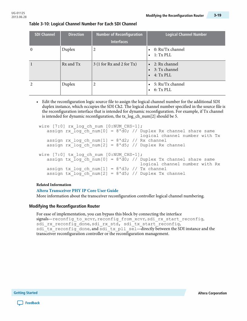
Table 3-10: Logical Channel Number For Each SDI Channel
Logical Channel NumberNumber of Reconfiguration
Interfaces
DirectionSDI Channel
• 0: Rx/Tx channel• 1: Tx PLL
2Duplex0
• 2: Rx channel• 3: Tx channel• 4: Tx PLL
3 (1 for Rx and 2 for Tx)Rx and Tx1
• 5: Rx/Tx channel• 6: Tx PLL
2Duplex2
• Edit the reconfiguration logic source file to assign the logical channel number for the additional SDIduplex instance, which occupies the SDI Ch2. The logical channel number specified in the source file isthe reconfiguration interface that is intended for dynamic reconfiguration. For example, if Tx channelis intended for dynamic reconfiguration, the tx_log_ch_num[2] should be 5.
wire [7:0] rx_log_ch_num [0:NUM_CHS-1];assign rx_log_ch_num[0] = 8'd0; // Duplex Rx channel share same
logical channel number with Txassign rx_log_ch_num[1] = 8'd2; // Rx channelassign rx_log_ch_num[2] = 8'd5; // Duplex Rx channel
wire [7:0] tx_log_ch_num [0:NUM_CHS-1];assign tx_log_ch_num[0] = 8'd0; // Duplex Tx channel share same
logical channel number with Rxassign tx_log_ch_num[1] = 8'd3; // Tx channelassign tx_log_ch_num[2] = 8'd5; // Duplex Tx channel
Related InformationAltera Transceiver PHY IP Core User GuideMore information about the transceiver reconfiguration controller logical channel numbering.
Modifying the Reconfiguration Router
For ease of implementation, you can bypass this block by connecting the interfacesignals—reconfig_to_xcvr, reconfig_from_xcvr, sdi_rx_start_reconfig,sdi_rx_reconfig_done, sdi_rx_std, sdi_tx_start_reconfig,sdi_tx_reconfig_done, and sdi_tx_pll_sel—directly between the SDI instance and thetransceiver reconfiguration controller or the reconfiguration management.
Altera CorporationGetting Started
Feedback
3-19Modifying the Reconfiguration RouterUG-011252013.06.28
4Functional Description
2013.06.28
UG-01125 Subscribe Feedback
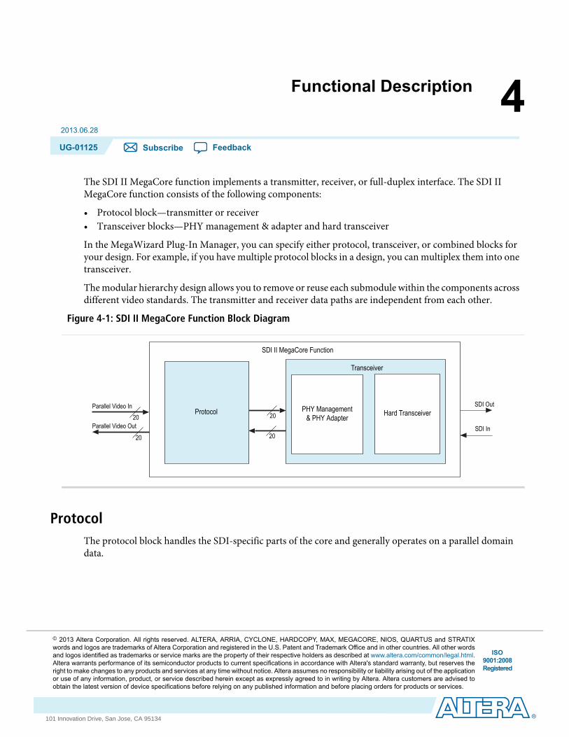
The SDI II MegaCore function implements a transmitter, receiver, or full-duplex interface. The SDI IIMegaCore function consists of the following components:
• Protocol block—transmitter or receiver• Transceiver blocks—PHY management & adapter and hard transceiver
In the MegaWizard Plug-In Manager, you can specify either protocol, transceiver, or combined blocks foryour design. For example, if you have multiple protocol blocks in a design, you can multiplex them into onetransceiver.
The modular hierarchy design allows you to remove or reuse each submodule within the components acrossdifferent video standards. The transmitter and receiver data paths are independent from each other.
Figure 4-1: SDI II MegaCore Function Block Diagram
Transceiver
SDI II MegaCore Function
Parallel Video In
Parallel Video Out
SDI Out
SDI In20
20
20
20
Protocol PHY Management& PHY Adapter Hard Transceiver
ProtocolThe protocol block handles the SDI-specific parts of the core and generally operates on a parallel domaindata.
ISO9001:2008Registered
© 2013 Altera Corporation. All rights reserved. ALTERA, ARRIA, CYCLONE, HARDCOPY, MAX, MEGACORE, NIOS, QUARTUS and STRATIXwords and logos are trademarks of Altera Corporation and registered in the U.S. Patent and Trademark Office and in other countries. All other wordsand logos identified as trademarks or service marks are the property of their respective holders as described at www.altera.com/common/legal.html.Altera warrants performance of its semiconductor products to current specifications in accordance with Altera's standard warranty, but reserves theright to make changes to any products and services at any time without notice. Altera assumes no responsibility or liability arising out of the applicationor use of any information, product, or service described herein except as expressly agreed to in writing by Altera. Altera customers are advised toobtain the latest version of device specifications before relying on any published information and before placing orders for products or services.
www.altera.com
101 Innovation Drive, San Jose, CA 95134
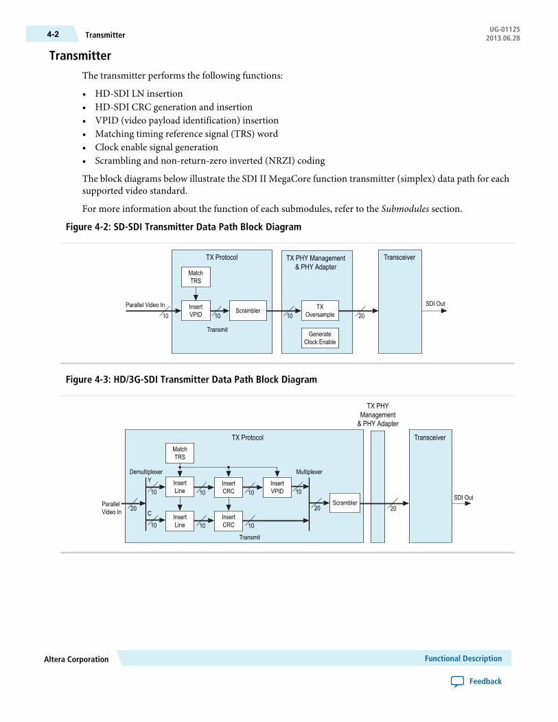
TransmitterThe transmitter performs the following functions:
• HD-SDI LN insertion• HD-SDI CRC generation and insertion• VPID (video payload identification) insertion• Matching timing reference signal (TRS) word• Clock enable signal generation• Scrambling and non-return-zero inverted (NRZI) coding
The block diagrams below illustrate the SDI II MegaCore function transmitter (simplex) data path for eachsupported video standard.
For more information about the function of each submodules, refer to the Submodules section.
Figure 4-2: SD-SDI Transmitter Data Path Block Diagram
MatchTRS
InsertVPID Scrambler TX
Oversample
GenerateClock Enable
Transmit
TX Protocol TX PHY Management& PHY Adapter
Transceiver
Parallel Video In10
SDI Out
10 10 20
Figure 4-3: HD/3G-SDI Transmitter Data Path Block Diagram
MatchTRS
InsertLine
Scrambler
InsertLine
20
Multiplexer
20
Transmit
TX Protocol
TX PHYManagement& PHY Adapter
Transceiver
ParallelVideo In
10SDI Out
10InsertCRC
InsertCRC
10InsertVPID10
10 10 10
20
DemultiplexerY
C
Functional DescriptionAltera Corporation
Feedback
UG-01125Transmitter4-2 2013.06.28
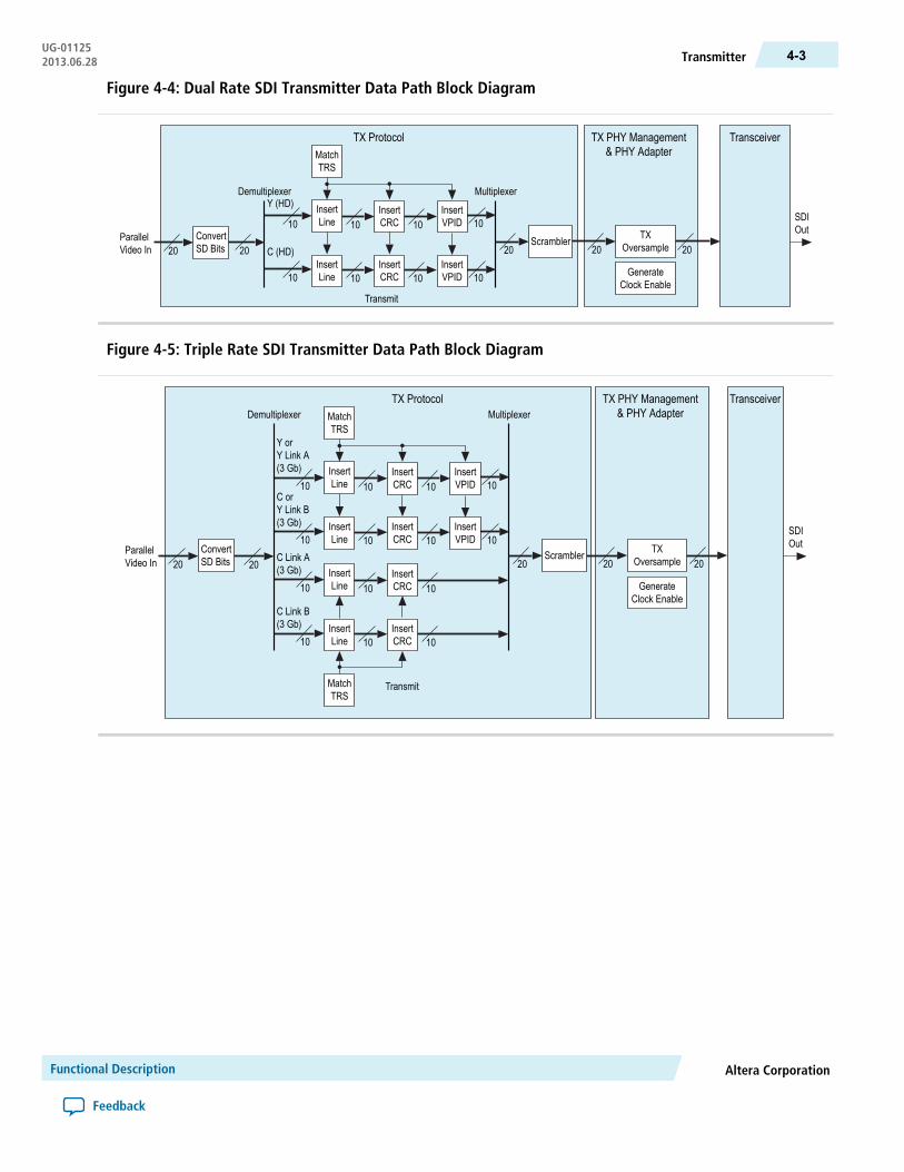
Figure 4-4: Dual Rate SDI Transmitter Data Path Block Diagram
MatchTRS
ConvertSD Bits
InsertLine
Scrambler
InsertLine
20
Multiplexer
2020TX
Oversample
GenerateClock Enable
TX PHY Management& PHY Adapter
20 20
Transmit
TX Protocol Transceiver
ParallelVideo In
10 SDIOut10
InsertCRC
InsertCRC
10InsertVPID10
10 10 10 10InsertVPID
DemultiplexerY (HD)
C (HD)
Figure 4-5: Triple Rate SDI Transmitter Data Path Block Diagram
MatchTRS
InsertLine
Scrambler
InsertLine
20
Multiplexer
2020TX
Oversample
GenerateClock Enable
TX PHY Management& PHY Adapter
20 20
Transmit
TX Protocol Transceiver
ParallelVideo In
10
SDIOut
10InsertCRC
InsertCRC
10InsertVPID10
10 10 10 10InsertVPID
MatchTRS
InsertLine
InsertLine
10InsertCRC
InsertCRC
10 10
10 10 10
C Link A(3 Gb)
C Link B(3 Gb)
Demultiplexer
Y orY Link A(3 Gb)
C orY Link B(3 Gb)
ConvertSD Bits
Altera CorporationFunctional Description
Feedback
4-3TransmitterUG-011252013.06.28
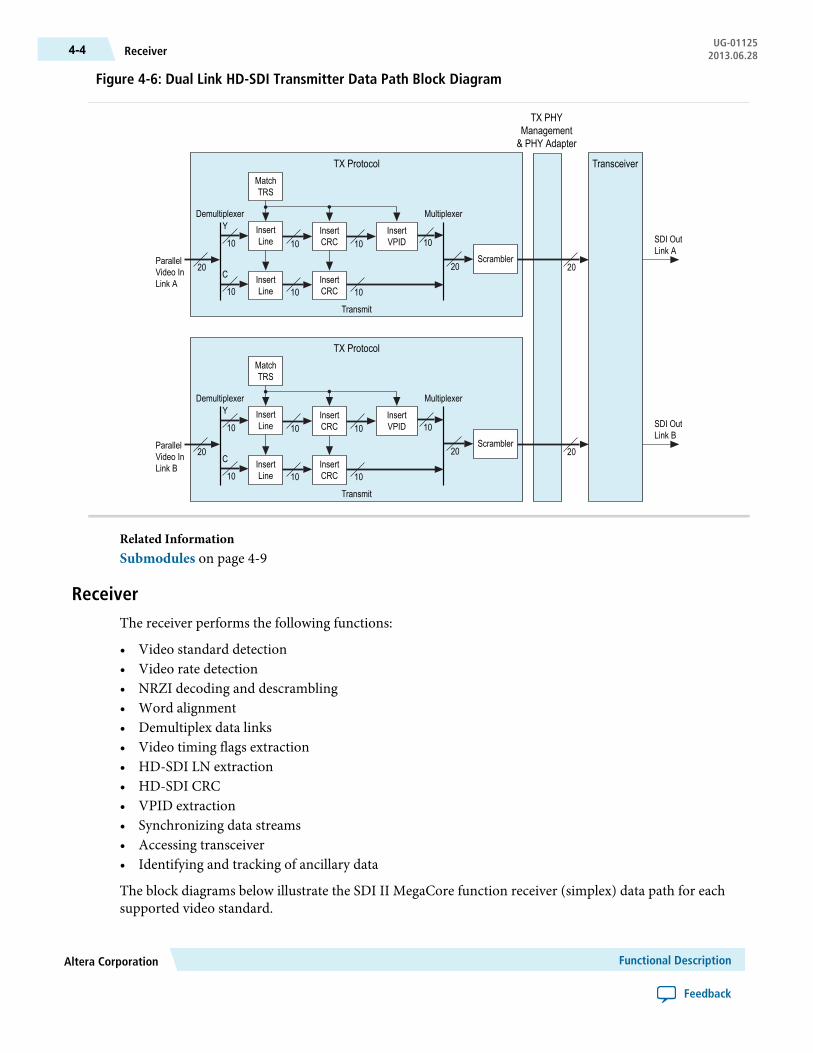
Figure 4-6: Dual Link HD-SDI Transmitter Data Path Block Diagram
MatchTRS
InsertLine
Scrambler
InsertLine
20
Multiplexer
20
Transmit
TX Protocol
TX PHYManagement& PHY Adapter
Transceiver
ParallelVideo InLink A
10 SDI OutLink A
10InsertCRC
InsertCRC
10InsertVPID10
10 10 10
MatchTRS
InsertLine
Scrambler
InsertLine
20
Multiplexer
20
Transmit
TX Protocol
ParallelVideo InLink B
10 SDI OutLink B
10InsertCRC
InsertCRC
10InsertVPID10
10 10 10
20
DemultiplexerY
C
20
DemultiplexerY
C
Related InformationSubmodules on page 4-9
ReceiverThe receiver performs the following functions:
• Video standard detection• Video rate detection• NRZI decoding and descrambling• Word alignment• Demultiplex data links• Video timing flags extraction• HD-SDI LN extraction• HD-SDI CRC• VPID extraction• Synchronizing data streams• Accessing transceiver• Identifying and tracking of ancillary data
The block diagrams below illustrate the SDI II MegaCore function receiver (simplex) data path for eachsupported video standard.
Functional DescriptionAltera Corporation
Feedback
UG-01125Receiver4-4 2013.06.28
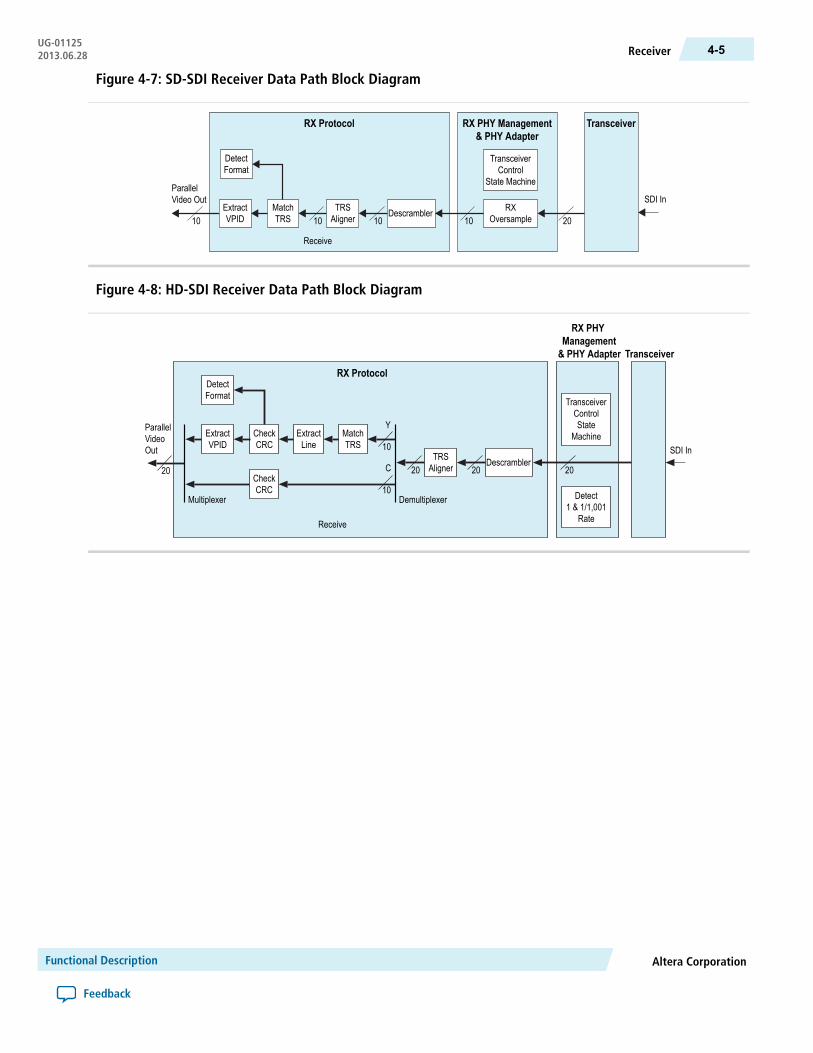
Figure 4-7: SD-SDI Receiver Data Path Block Diagram
DetectFormat
TRSAligner Descrambler RX
Oversample
TransceiverControl
State Machine
Receive
RX Protocol RX PHY Management& PHY Adapter
Transceiver
ParallelVideo Out
10 10MatchTRS 10
ExtractVPID 10 20
SDI In
Figure 4-8: HD-SDI Receiver Data Path Block Diagram
DetectFormat
TRSAligner Descrambler
Detect1 & 1/1,001
Rate
TransceiverControlState
Machine
Receive
RX Protocol
RX PHYManagement& PHY Adapter Transceiver
ParallelVideoOut
20 20
MatchTRS 10
ExtractLine
20
CheckCRC
ExtractVPID
CheckCRC
DemultiplexerMultiplexer
Y
C
10
20
SDI In
Altera CorporationFunctional Description
Feedback
4-5ReceiverUG-011252013.06.28
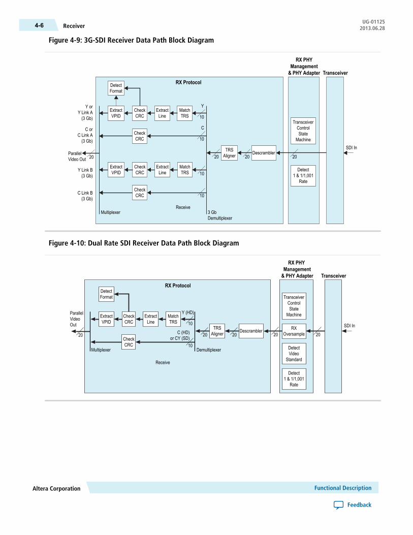
Figure 4-9: 3G-SDI Receiver Data Path Block Diagram
DetectFormat
TRSAligner Descrambler
Detect1 & 1/1,001
Rate
TransceiverControlState
Machine
Receive
RX Protocol
RX PHYManagement& PHY Adapter Transceiver
ParallelVideo Out 20 20
MatchTRS 10
ExtractLine
20
CheckCRC
ExtractVPID
CheckCRC
3 GbDemultiplexer
Multiplexer
Y
C
10
MatchTRS 10
ExtractLine
CheckCRC
ExtractVPID
CheckCRC 10
Y Link B(3 Gb)
C Link B(3 Gb)
Y orY Link A(3 Gb)
C orC Link A(3 Gb)
20
SDI In
Figure 4-10: Dual Rate SDI Receiver Data Path Block Diagram
DetectFormat
TRSAligner Descrambler
DetectVideo
Standard
TransceiverControlState
Machine
Receive
RX Protocol
RX PHYManagement& PHY Adapter Transceiver
ParallelVideoOut
20 20
MatchTRS 10
ExtractLine
20
CheckCRC
ExtractVPID
CheckCRC
DemultiplexerMultiplexer
Y (HD)
C (HD)or CY (SD)
10
RXOversample20 20
SDI In
Detect1 & 1/1,001
Rate
Functional DescriptionAltera Corporation
Feedback
UG-01125Receiver4-6 2013.06.28
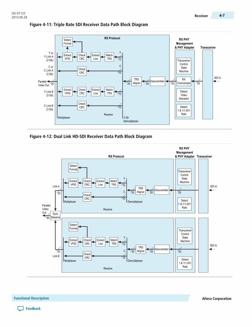
Figure 4-11: Triple Rate SDI Receiver Data Path Block Diagram
DetectVideo
Standard
TransceiverControlState
Machine
RX PHYManagement& PHY Adapter Transceiver
DetectFormat
TRSAligner Descrambler
Receive
RX Protocol
ParallelVideo Out 20 20
MatchTRS 10
ExtractLine
20
CheckCRC
ExtractVPID
CheckCRC
3 GbDemultiplexer
Multiplexer
Y
C
10
MatchTRS 10
ExtractLine
CheckCRC
ExtractVPID
CheckCRC 10
Y Link B(3 Gb)
C Link B(3 Gb)
Y orY Link A(3 Gb)
C orC Link A(3 Gb)
RXOversample20 20
SDI In
Detect1 & 1/1,001
Rate
Figure 4-12: Dual Link HD-SDI Receiver Data Path Block Diagram
DetectFormat
TRSAligner Descrambler
Detect1 & 1/1,001
Rate
TransceiverControlState
Machine
Receive
RX Protocol
RX PHYManagement& PHY Adapter Transceiver
ParallelVideoOut
Link A
Link B
40
20
MatchTRS 10
ExtractLine
20
CheckCRC
ExtractVPID
CheckCRC
DemultiplexerMultiplexer
Y
C
10
20
SDI In
SDI In
DetectFormat
TRSAligner Descrambler
Detect1 & 1/1,001
Rate
TransceiverControlState
Machine
Receive
20 20
MatchTRS 10
ExtractLine
20
CheckCRC
ExtractVPID
CheckCRC
DemultiplexerMultiplexer
Y
C
10
20
SyncStreams
20
Altera CorporationFunctional Description
Feedback
4-7ReceiverUG-011252013.06.28
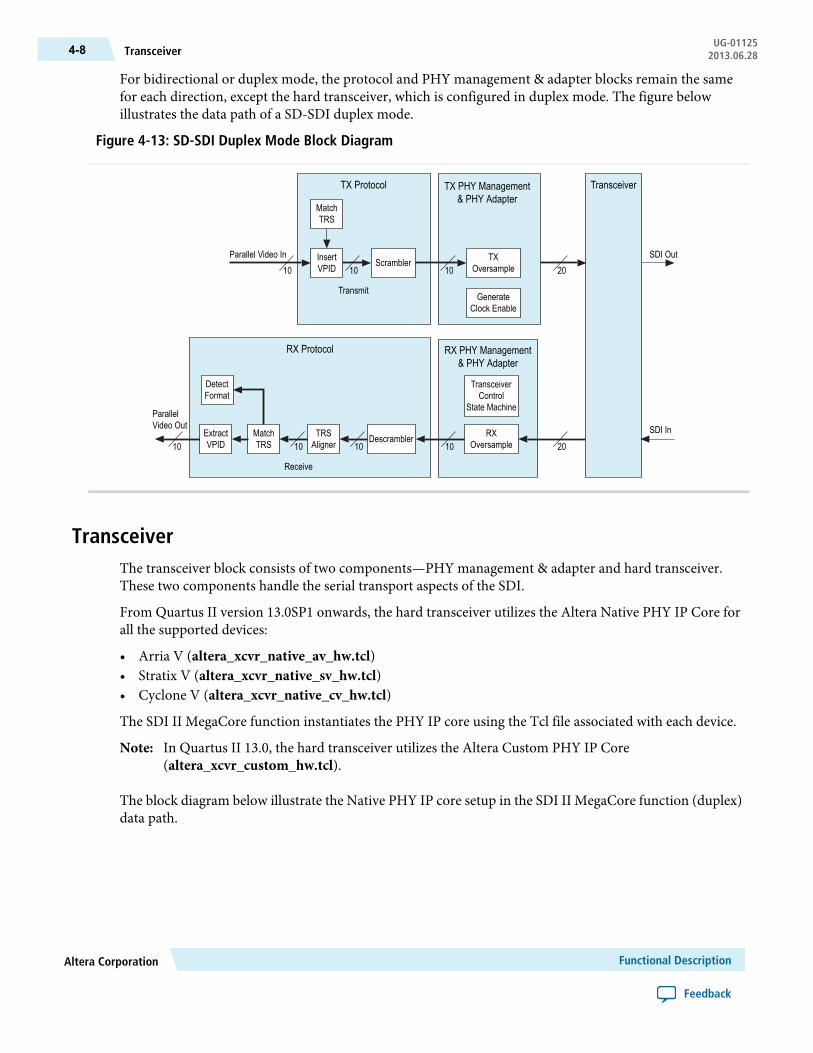
For bidirectional or duplex mode, the protocol and PHY management & adapter blocks remain the samefor each direction, except the hard transceiver, which is configured in duplex mode. The figure belowillustrates the data path of a SD-SDI duplex mode.
Figure 4-13: SD-SDI Duplex Mode Block Diagram
TX Protocol
DetectFormat
TRSAligner Descrambler RX
Oversample
TransceiverControl
State Machine
Receive
RX Protocol RX PHY Management& PHY Adapter
ParallelVideo Out
10 10MatchTRS 10
ExtractVPID 10 20
MatchTRS
InsertVPID Scrambler TX
Oversample
GenerateClock Enable
Transmit
TX PHY Management& PHY Adapter
Transceiver
Parallel Video In10
SDI Out10 10 20
SDI In
TransceiverThe transceiver block consists of two components—PHY management & adapter and hard transceiver.These two components handle the serial transport aspects of the SDI.
From Quartus II version 13.0SP1 onwards, the hard transceiver utilizes the Altera Native PHY IP Core forall the supported devices:
• Arria V (altera_xcvr_native_av_hw.tcl)• Stratix V (altera_xcvr_native_sv_hw.tcl)• Cyclone V (altera_xcvr_native_cv_hw.tcl)
The SDI II MegaCore function instantiates the PHY IP core using the Tcl file associated with each device.
In Quartus II 13.0, the hard transceiver utilizes the Altera Custom PHY IP Core(altera_xcvr_custom_hw.tcl).
Note:
The block diagram below illustrate the Native PHY IP core setup in the SDI II MegaCore function (duplex)data path.
Functional DescriptionAltera Corporation
Feedback
UG-01125Transceiver4-8 2013.06.28

Figure 4-15: Altera Native PHY IP Core Setup in Duplex Mode
TheAlteraNative PHY IPCore does not include an embedded reset controller and anAvalon-MM interface.This PHY IP core exposes all signals directly as ports. To implement reset functionality for a new IP core,the transceiver reset controller is required to handle all the transceiver reset sequencing. The transceiverreset controller controls the embedded reset controller and also manages additional control options such asautomatic or manual reset recovery mode.
RXOversample
TransceiverControl
State Machine
RX PHY Management& PHY Adapter
20 20
TXOversample
GenerateClock Enable
TX PHY Management& PHY Adapter
Transceiver
SDI Out20 20
SDI In
DetectVideo
Standard
AlteraNative PHYIP Core
TransceiverReset Controller
(RX)
TransceiverReset Controller
(TX)
Detect1 & 1/1,001
Rate
Related InformationAltera Transceiver PHY IP Core User GuideMore information about the Altera Native PHY IP Core.
SubmodulesYou can reuse the submodules in the protocol and transceiver components across different video standard.The SDI II MegaCore function consists of the following submodules:
• Insert Line• Insert/Check CRC• Insert VPID• Match TRS• Scrambler• Tx Oversample• Rx Oversample
Altera CorporationFunctional Description
Feedback
4-9SubmodulesUG-011252013.06.28
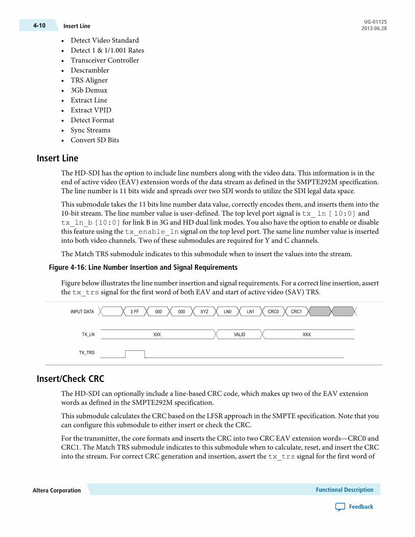
• Detect Video Standard• Detect 1 & 1/1.001 Rates• Transceiver Controller• Descrambler• TRS Aligner• 3Gb Demux• Extract Line• Extract VPID• Detect Format• Sync Streams• Convert SD Bits
Insert LineThe HD-SDI has the option to include line numbers along with the video data. This information is in theend of active video (EAV) extension words of the data stream as defined in the SMPTE292M specification.The line number is 11 bits wide and spreads over two SDI words to utilize the SDI legal data space.
This submodule takes the 11 bits line number data value, correctly encodes them, and inserts them into the10-bit stream. The line number value is user-defined. The top level port signal is tx_ ln [ 10:0] andtx_ln_b [10:0] for link B in 3G and HD dual link modes. You also have the option to enable or disablethis feature using the tx_enable_ln signal on the top level port. The same line number value is insertedinto both video channels. Two of these submodules are required for Y and C channels.
The Match TRS submodule indicates to this submodule when to insert the values into the stream.
Figure 4-16: Line Number Insertion and Signal Requirements
Figure below illustrates the line number insertion and signal requirements. For a correct line insertion, assertthe tx_trs signal for the first word of both EAV and start of active video (SAV) TRS.
3 FF 000 000 XYZ LN0 CRC0 CRC1LN1
XXXVALIDXXX
INPUT DATA
TX_LN
TX_TRS
Insert/Check CRCThe HD-SDI can optionally include a line-based CRC code, which makes up two of the EAV extensionwords as defined in the SMPTE292M specification.
This submodule calculates the CRC based on the LFSR approach in the SMPTE specification. Note that youcan configure this submodule to either insert or check the CRC.
For the transmitter, the core formats and inserts the CRC into two CRC EAV extension words—CRC0 andCRC1. The Match TRS submodule indicates to this submodule when to calculate, reset, and insert the CRCinto the stream. For correct CRC generation and insertion, assert the tx_trs signal for the first word of
Functional DescriptionAltera Corporation
Feedback
UG-01125Insert Line4-10 2013.06.28
both EAV and SAV TRS as shown in the Insert Line timing diagram. Perform CRC insertion only whenthe top level port, tx_enable_crc, is set to logic 1.
For the receiver, the core checks the CRC against the value of CRC0 and CRC1 that appear in the incomingstream. If there is amismatch between the locally calculated value and the value in the stream, this submoduleindicates an error. The Match TRS submodule indicates when the CRC0 and CRC1 words are present inthe incoming data stream.
Insert VPIDThe SMPTE352M specification defines an ancillary packet type that provides specific information about thevideo payload carried by a digital interface. These VPID packets carry information such as the interface type,sampling structure, component bit depth, and picture update rate. Recent SMPTE interfaces such as duallink HD-SDI and 3G-SDI require the VPID packets because it is very difficult to properly interpret the videodata without the packet information from the VPID packets.
The VPID packet must be on specific video lines locations at the beginning of the horizontal ancillary(HANC) space, which is right after the EAV, or CRC words that follow the EAV on the interfaces using CRCwords.
Table 4-1: VPID Packet Location
Line NumberFieldVideo Format
131525i
2762
91625i
3222
1011080i
5722
13—525p
9—625p
10—720p
10—1080p
For dual link HD-SDI interface, the VPID packets are placed only in the Y data stream of both links. Thissubmodule in the transmitter data path modifies the Y data stream that passes through.
This submodule introduces a latency of a few clock cycles. The C data stream is delayed by a fewclock cycles to keep it synchronized with the Y data stream.
Note:
Altera CorporationFunctional Description
Feedback
4-11Insert VPIDUG-011252013.06.28
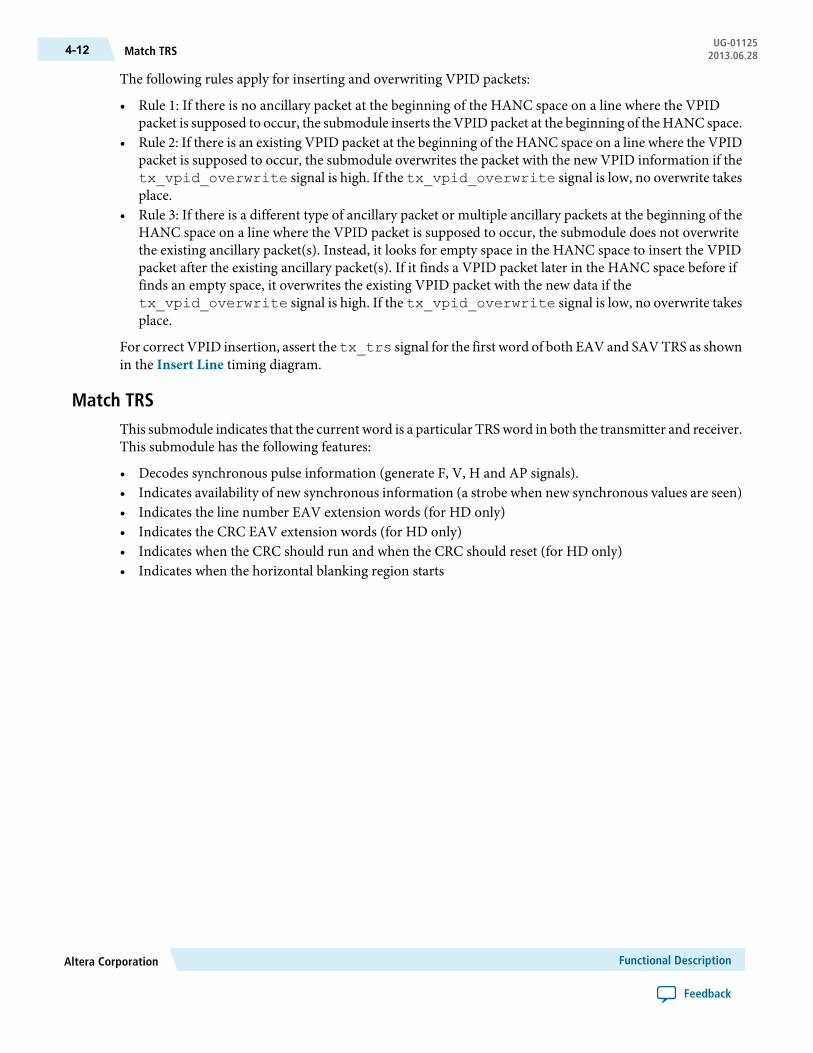
The following rules apply for inserting and overwriting VPID packets:
• Rule 1: If there is no ancillary packet at the beginning of the HANC space on a line where the VPIDpacket is supposed to occur, the submodule inserts the VPID packet at the beginning of the HANC space.
• Rule 2: If there is an existing VPID packet at the beginning of the HANC space on a line where the VPIDpacket is supposed to occur, the submodule overwrites the packet with the new VPID information if thetx_vpid_overwrite signal is high. If the tx_vpid_overwrite signal is low, no overwrite takesplace.
• Rule 3: If there is a different type of ancillary packet or multiple ancillary packets at the beginning of theHANC space on a line where the VPID packet is supposed to occur, the submodule does not overwritethe existing ancillary packet(s). Instead, it looks for empty space in the HANC space to insert the VPIDpacket after the existing ancillary packet(s). If it finds a VPID packet later in the HANC space before iffinds an empty space, it overwrites the existing VPID packet with the new data if thetx_vpid_overwrite signal is high. If the tx_vpid_overwrite signal is low, no overwrite takesplace.
For correct VPID insertion, assert thetx_trs signal for the first word of both EAV and SAV TRS as shownin the Insert Line timing diagram.
Match TRSThis submodule indicates that the current word is a particular TRS word in both the transmitter and receiver.This submodule has the following features:
• Decodes synchronous pulse information (generate F, V, H and AP signals).• Indicates availability of new synchronous information (a strobe when new synchronous values are seen)• Indicates the line number EAV extension words (for HD only)• Indicates the CRC EAV extension words (for HD only)• Indicates when the CRC should run and when the CRC should reset (for HD only)• Indicates when the horizontal blanking region starts
Functional DescriptionAltera Corporation
Feedback
UG-01125Match TRS4-12 2013.06.28
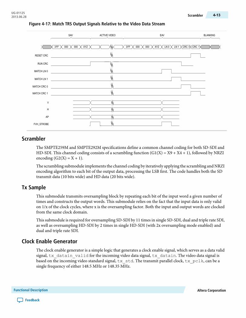
Figure 4-17: Match TRS Output Signals Relative to the Video Data Stream
3FF 000 000 XYZ 3FF 000 000 XYZ LN 0 CRC 0 CRC 1LN 1
SAV EAVACTIVE VIDEO BLANKING
RESET CRC
RUN CRC
MATCH LN 0
MATCH LN 1
MATCH CRC 0
MATCH CRC 1
V
H
AP
FVH_STROBE
ScramblerThe SMPTE259M and SMPTE292M specifications define a common channel coding for both SD-SDI andHD-SDI. This channel coding consists of a scrambling function (G1(X) = X9 + X4 + 1), followed by NRZIencoding (G2(X) = X + 1).
The scrambling submodule implements the channel coding by iteratively applying the scrambling andNRZIencoding algorithm to each bit of the output data, processing the LSB first. The code handles both the SDtransmit data (10 bits wide) and HD data (20 bits wide).
Tx SampleThis submodule transmits oversampling block by repeating each bit of the input word a given number oftimes and constructs the output words. This submodule relies on the fact that the input data is only validon 1/x of the clock cycles, where x is the oversampling factor. Both the input and output words are clockedfrom the same clock domain.
This submodule is required for oversampling SD-SDI by 11 times in single SD-SDI, dual and triple rate SDI,as well as oversampling HD-SDI by 2 times in single HD-SDI (with 2x oversampling mode enabled) anddual and triple rate SDI.
Clock Enable GeneratorThe clock enable generator is a simple logic that generates a clock enable signal, which serves as a data validsignal, tx_datain_valid for the incoming video data signal, tx_datain. The video data signal isbased on the incoming video standard signal, tx_std. The transmit parallel clock, tx_pclk, can be asingle frequency of either 148.5 MHz or 148.35 MHz.
Altera CorporationFunctional Description
Feedback
4-13ScramblerUG-011252013.06.28
The clock enable generator generates a clock signal in the following conditions:
• If the tx_datain signal is SD—generate a tx_datain_valid pulse every 5th and 11th clock cycleof the tx_pclk domain.
• If the tx_datain signal is HD—generate a tx_datain_valid pulse every other clock cycle of thetx_pclk domain.
• If the tx_datain signal is neither SD nor HD—the tx_datain_valid pulse remains high for 3G.
Figure 4-18: Triple Rate Transmit Clocking Scheme
Figure below illustrates the behavior of the tx_datain_valid pulse in each video standard.
tx_pclk(148.5 @ 148.35 MHz)
SD_SDI
tx_datain_valid
tx_datain_valid
tx_datain_valid
5 11 5 11
tx_pclk(148.5 @ 148.35 MHz)
HD_SDI
5 11 5 11
tx_pclk(148.5 @ 148.35 MHz)
3G_SDI
5 11 5 11
Rx SampleThis submodule extracts data from the oversampled incoming data stream. In oversampling schemes, eachbit is repeated many times. For example, a stream of 0 1 0 1 may look like 000111000111 at the oversampleclock or data rate.
This submodule examines the incoming data stream for logic transitions. These transitions mark theboundaries of the incoming data bit. It is desirable to extract a sample at a point between these two boundaries.This submodule identifies a transition, then extracts the sample X clocks after this transition. When notransitions are present in the incoming data stream, the submodule uses knowledge of oversampling rate tocontinuously sample the incoming data at a particular rate. When the next transition is present, the schemeresets and the sampling aligns to this new transition.
Functional DescriptionAltera Corporation
Feedback
UG-01125Rx Sample4-14 2013.06.28
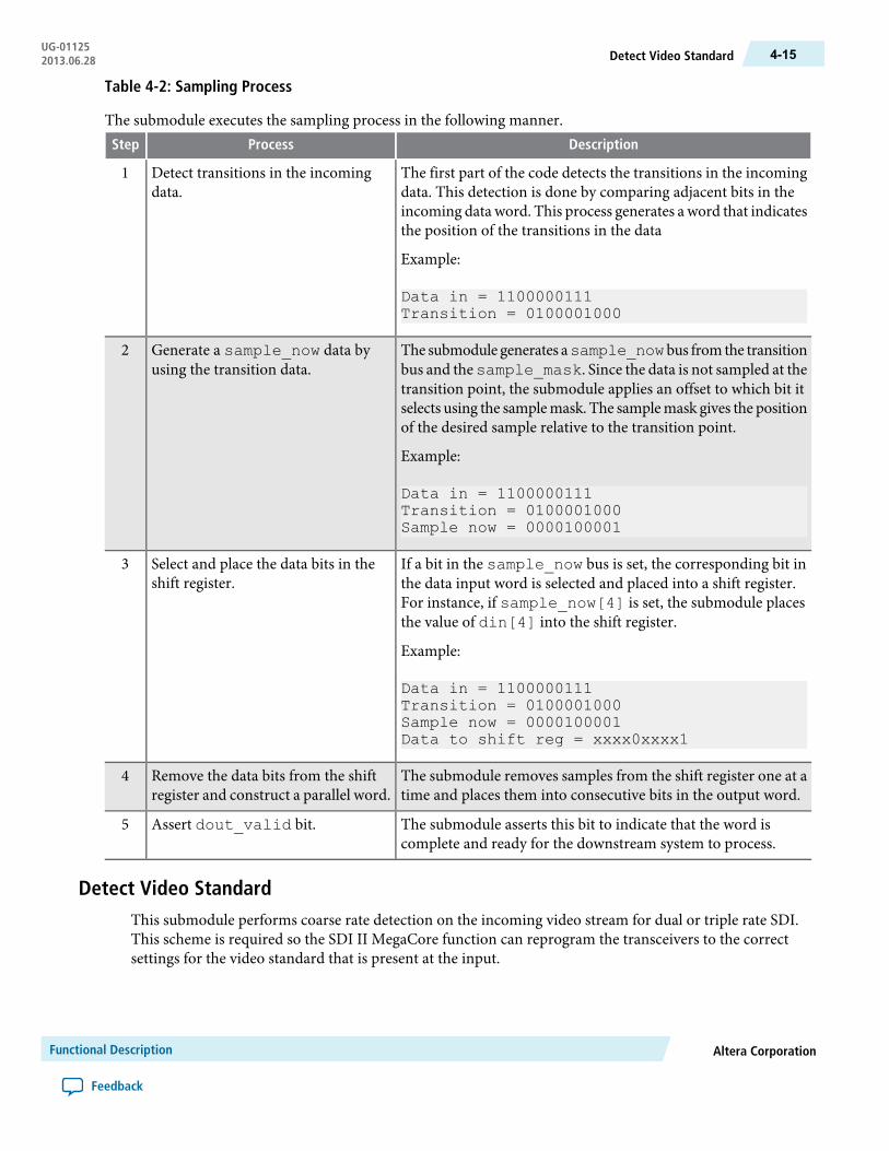
Table 4-2: Sampling Process
The submodule executes the sampling process in the following manner.DescriptionProcessStep
The first part of the code detects the transitions in the incomingdata. This detection is done by comparing adjacent bits in theincoming data word. This process generates a word that indicatesthe position of the transitions in the data
Example:
Data in = 1100000111Transition = 0100001000
Detect transitions in the incomingdata.
1
The submodule generates asample_nowbus from the transitionbus and thesample_mask. Since the data is not sampled at thetransition point, the submodule applies an offset to which bit itselects using the samplemask. The samplemask gives the positionof the desired sample relative to the transition point.
Example:
Data in = 1100000111Transition = 0100001000Sample now = 0000100001
Generate a sample_now data byusing the transition data.
2
If a bit in the sample_now bus is set, the corresponding bit inthe data input word is selected and placed into a shift register.For instance, if sample_now[4] is set, the submodule placesthe value of din[4] into the shift register.
Example:
Data in = 1100000111Transition = 0100001000Sample now = 0000100001Data to shift reg = xxxx0xxxx1
Select and place the data bits in theshift register.
3
The submodule removes samples from the shift register one at atime and places them into consecutive bits in the output word.
Remove the data bits from the shiftregister and construct a parallel word.
4
The submodule asserts this bit to indicate that the word iscomplete and ready for the downstream system to process.
Assert dout_valid bit.5
Detect Video StandardThis submodule performs coarse rate detection on the incoming video stream for dual or triple rate SDI.This scheme is required so the SDI II MegaCore function can reprogram the transceivers to the correctsettings for the video standard that is present at the input.
Altera CorporationFunctional Description
Feedback
4-15Detect Video StandardUG-011252013.06.28
The submodule executes the detection process in the following manner:
1. Look for transitions in the incoming data words by comparing each bit with the adjacent bit in theincoming word. Then, generate a bus with one bit set for each transition or edge seen.
2. Count the number of bit sets in the bus and return a value, which represents the number of edges presentin a particular input data word.
3. Count the total number of edges seen over a given number of input words using an accumulator. Then,add the number of transitions seen in the current input word to a running total of transitions seen sincethe accumulator was reset.
4. Compare the total number of edges with a fixed set of values determined by experimentation. The actualthresholds are relative to the data rates of the three standards.
This submodule asserts the rate_detect_done flag to indicate to the transceiver controller submodulethat rate detection has been performed. This approach is further described in the Transceiver Controllersection.
Related InformationTransceiver Controller on page 4-16
Detect 1 and 1/1.001 RatesThis submodule indicates if the incoming video stream is running at PAL (1) or NTSC (1/1.001) rate. Theoutput port signal,rx_clkout_is_ntsc_paln is set to 0 if the submodule detects the incoming streamas PAL (148.5 MHz or 74.25 MHz recovered clock) and set to 1 if the incoming stream is detected as NTSC(148.35 MHz or 74.175 MHz recovered clock).
For correct video rate detection, you must set the top level port signal, rx_coreclk_is_ntsc_paln,to the following bit:
• 0 if the rx_coreclk signal is 148.5 MHz or 74.25 MHz• 1 if the rx_coreclk signal is 148.35 MHz or 74.175 MHz
Transceiver ControllerThe transceiver controller controls the transceiver to achieve the desired receiver functionality for the SDI.
When the interface receives SD-SDI, the transceiver receiver PLL locks to the receiver reference clock.
When the interface receives HD-SDI, the transceiver receiver PLL is first trained by locking to the receiverreference clock. When the PLL is locked, it can then track the actual receiver data rate. If a period of timepasses without a valid SDI signal, the PLL is retrained with the reference clock and the process repeats.
The transceiver controller uses a different approach to detect the incoming video standard. Instead of settingthe core to each of the standards andwaiting to see if lock is achieved, the core directly analyses the incomingstream and try to determine the rate. This is done by looking at the edge density, or by number of transitionsin the incoming stream as described in the Detect Video Standard section.
Firstly, the core is set into 3G mode (transceiver running at 2.97 Gbps) and in lock-to-refclk (LTR) mode.It is essentially running in a fixed frequency sampling mode. The core examines for transitions in the data
Functional DescriptionAltera Corporation
Feedback
UG-01125Detect 1 and 1/1.001 Rates4-16 2013.06.28
stream. The number of transitions in the incoming stream is counted over a fixed period of time and isdetermined in the following manner:
• If the incoming stream is 3G, you would see X number of transitions.• If the incoming stream is HD (1.485 Gbps), you would see X/2 transitions.• If the incoming stream is SD, you would see X/11 transitions.
Compare the edge count value with a number of fixed values that correspond to the thresholds of the videostandards. This approach works because the scrambling algorithm in the SDI guarantees a maximum anda minimum number of transitions in the SDI stream.
The output of this circuit determines if the transceiver requires dynamic reconfiguration to a new mode.The dual and triple rate SDI core uses 11x oversampling for the reception of SD-SDI. This means that yourequire only two transceiver setups since the rates for 3G-SDI and 11x SD-SDI are the same.
The transceiver controller uses the presence (or absence) of TRSs on the stream to determine if the SDIsignal is correctly received. The detect format submodule indicates to the transceiver controller that thereceiver is acquiring some valid SDI samples when it detects a single and valid TRS. The transceiver controlleronly deasserts this flag when it does not detect any EAV sequences within the number of consecutive linesspecified. At this point, the transceiver controller state machine resets and performs the relock algorithm.
The receive transceivers can be set into one of two modes, manual or automatic. In automatic mode, a statemachine internal to the transceiver controls the training. In manual mode, the external logic must take careof the transceiver training by using either lock-to-refclk (LTR) or lock-to-data (LTD) mode.
In LTRmode, a statemachine internal to the receive transceiver uses the applied reference clock for operation.In this mode, the core samples the incoming data using the refclk signal and does not perform clockrecovery. The sampling clock is not locked to the incoming data stream. This mode is used for transceivertraining and in the oversampling modes of SD-SDI. In this mode, the rx_clkout signal of the transceiveris a mirror of the reference clock.
In LTD mode, a state machine internal to the receive transceiver uses the clock generated by the CDRcircuitry. The CDR extracts a clock from the incoming data stream and uses the clock to sample the incomingdata. The sampling clock locks to the incoming data. This mode can only be used once the transceiver hasbeen trained. Use this mode to recover data for HD and 3G streams. In this mode, the rx_clkout signalof the transceiver locks to the data.
Related InformationDetect Video Standard on page 4-15
DescramblerThis submodule implements data descrambling as defined in the SMPTE259 and SMPTE292 specifications.This submodule is similar to the scrambler submodule, where it implements the reverse of the scramblingapplied to the data. This submodule uses an LFSR and also implements NRZI.
TRS AlignerThe TRS aligner word aligns the descrambled receiver data until the bit order of the output data and theoriginal video data are the same. The EAV and SAV sequences determine the correct word alignment.
Altera CorporationFunctional Description
Feedback
4-17DescramblerUG-011252013.06.28
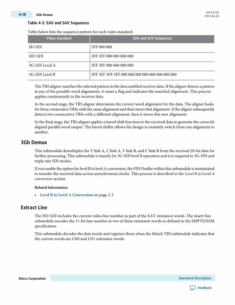
Table 4-3: EAV and SAV Sequences
Table below lists the sequence pattern for each video standard.EAV and SAV SequencesVideo Standard
3FF 000 000SD-SDI
3FF 3FF 000 000 000 000HD-SDI
3FF 3FF 000 000 000 0003G-SDI Level A
3FF 3FF 3FF 3FF 000 000 000 000 000 000 000 0003G-SDI Level B
TheTRS alignermatches the selected pattern in the descrambled receiver data. If the aligner detects a patternat any of the possible word alignments, it raises a flag and indicates the matched alignment. This processapplies continuously to the receiver data.
In the second stage, the TRS aligner determines the correct word alignment for the data. The aligner looksfor three consecutive TRSswith the same alignment and then stores that alignment. If the aligner subsequentlydetects two consecutive TRSs with a different alignment, then it stores this new alignment.
In the final stage, the TRS aligner applies a barrel shift function to the received data to generate the correctlyaligned parallel word output. The barrel shifter allows the design to instantly switch from one alignment toanother.
3Gb DemuxThis submodule demultiplex the Y link A, C link A, Y link B, and C link B from the received 20-bit data forfurther processing. This submodule is mainly for 3G-SDI level B operation and it is required in 3G-SDI andtriple rate SDI modes.
If you enable the option for level B to level A conversion, the FIFObuffer within this submodule is instantiatedto transfer the received data across asynchronous clocks. This process is described in the Level B to Level Aconversion section.
Related Information
• Level B to Level A Conversion on page 2-3
Extract LineThe HD-SDI includes the current video line number as part of the EAV extension words. The insert linesubmodule encodes the 11-bit line number in two of these extension words as defined in the SMPTE292Mspecification.
This submodule decodes the data words and registers them when the Match TRS submodule indicates thatthe current words are LN0 and LN1 extension words.
Functional DescriptionAltera Corporation
Feedback
UG-011253Gb Demux4-18 2013.06.28
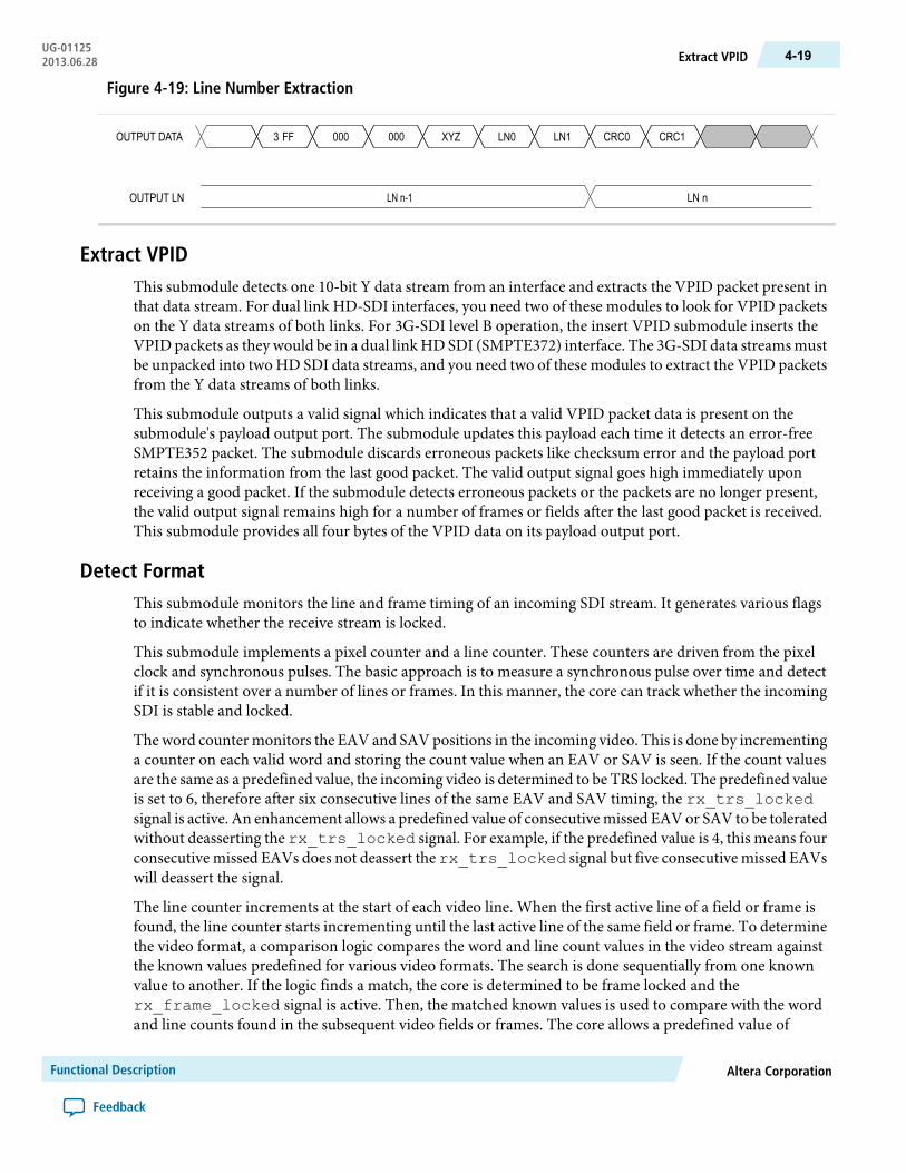
Figure 4-19: Line Number Extraction
3 FF 000 000 XYZ LN0 CRC0 CRC1LN1
LN nLN n-1
OUTPUT DATA
OUTPUT LN
Extract VPIDThis submodule detects one 10-bit Y data stream from an interface and extracts the VPID packet present inthat data stream. For dual link HD-SDI interfaces, you need two of these modules to look for VPID packetson the Y data streams of both links. For 3G-SDI level B operation, the insert VPID submodule inserts theVPID packets as they would be in a dual link HD SDI (SMPTE372) interface. The 3G-SDI data streams mustbe unpacked into two HD SDI data streams, and you need two of these modules to extract the VPID packetsfrom the Y data streams of both links.
This submodule outputs a valid signal which indicates that a valid VPID packet data is present on thesubmodule's payload output port. The submodule updates this payload each time it detects an error-freeSMPTE352 packet. The submodule discards erroneous packets like checksum error and the payload portretains the information from the last good packet. The valid output signal goes high immediately uponreceiving a good packet. If the submodule detects erroneous packets or the packets are no longer present,the valid output signal remains high for a number of frames or fields after the last good packet is received.This submodule provides all four bytes of the VPID data on its payload output port.
Detect FormatThis submodule monitors the line and frame timing of an incoming SDI stream. It generates various flagsto indicate whether the receive stream is locked.
This submodule implements a pixel counter and a line counter. These counters are driven from the pixelclock and synchronous pulses. The basic approach is to measure a synchronous pulse over time and detectif it is consistent over a number of lines or frames. In this manner, the core can track whether the incomingSDI is stable and locked.
Theword countermonitors the EAV and SAVpositions in the incoming video. This is done by incrementinga counter on each valid word and storing the count value when an EAV or SAV is seen. If the count valuesare the same as a predefined value, the incoming video is determined to be TRS locked. The predefined valueis set to 6, therefore after six consecutive lines of the same EAV and SAV timing, the rx_trs_lockedsignal is active. An enhancement allows a predefined value of consecutive missed EAV or SAV to be toleratedwithout deasserting the rx_trs_locked signal. For example, if the predefined value is 4, this means fourconsecutive missed EAVs does not deassert the rx_trs_locked signal but five consecutive missed EAVswill deassert the signal.
The line counter increments at the start of each video line. When the first active line of a field or frame isfound, the line counter starts incrementing until the last active line of the same field or frame. To determinethe video format, a comparison logic compares the word and line count values in the video stream againstthe known values predefined for various video formats. The search is done sequentially from one knownvalue to another. If the logic finds a match, the core is determined to be frame locked and therx_frame_locked signal is active. Then, the matched known values is used to compare with the wordand line counts found in the subsequent video fields or frames. The core allows a predefined value of
Altera CorporationFunctional Description
Feedback
4-19Extract VPIDUG-011252013.06.28
consecutivemismatch fields or frames to be toleratedwithout therx_frame_locked signal. For example,if the predefined value is 4, this means four consecutive mismatch fields or frames does not deassert therx_frame_locked signal but five consecutive mismatch fields or frames will deassert the signal.
Sync StreamsThis submodule is required in the HD-SDI dual link receiver as it synchronizes and deskews both datastreams received by two separate transceivers of link A and link B.
This submodule contains two FIFO buffers, where each buffer holds and transfers received data andmiscellaneous signals like line number and CRC error for each link. The read operation on both FIFO buffersbegin when the control state machine detects that both links are alignment locked (rx_align_lockedis active). If a TRS is first seen on link A but not link B, the control state machine halts reading from FIFObuffer link A until TRS is seen on link B. This is also similar to the case when a TRS is first seen on link Bbut not link A. Then, the core is considered locked and rx_dl_locked signal is active. The SMPTE 372specification defines that the timing difference between link A and link B must not exceed 40 ns.
When the core is locked, the control state machine continuously sees TRS from both FIFO buffers at thesame time. If not, both linksmight have unaligned but it does not necessarily becomeTRS or frame unlocked.The control statemachine aligns both links at the next TRSwithout deasserting therx_dl_locked signal.The control state machine only deasserts the rx_dl_locked signal when the rx_trs_locked signalis deasserted.
Convert SD BitsThis submodule is enabledwhen you set the SD InterfaceBitWidth parameter option to 20. This submoduleconverts the SD parallel data in 20 bits back to 10 bits format required for further processing.
This submodule contains a clock enable generator to generate two data valid pulses at every 11th clock cycleof the tx_pclk domain. Each time the data valid signal is asserted, this block will alternately output thelower 10 bits and upper 10 bits of the SD 20-bit interface data to the downstream logic.
Clocking SchemeTo reduce design complexity and logic resource utilization, the SDI II MegaCore function implements aclock enable generator submodule to replace both the PLL at the parallel clock domain and the FIFO bufferin the transceiver interface block.
For the oversampling rate, the SDI II MegaCore function clocking scheme is standardized by applying anoversampling rate of 11 times for SD-SDI, dual, and triple rate modes.
Related InformationClock Enable Generator on page 4-13
SDI II MegaCore Function SignalsThe following tables list the SDI II MegaCore function signals by components.
• Protocol blocks—transmitter, receiver• Transceiver blocks—PHY management, PHY adapter, hard transceiver
Functional DescriptionAltera Corporation
Feedback
UG-01125Sync Streams4-20 2013.06.28
Table 4-4: Transmitter Protocol Signals
DescriptionDirectionWidthSignal
Transmitter reset signal. This signal is active high and level sensitive.For Arria V and Stratix V devices, this reset signal must besynchronous to tx_pclk clock domain. For Cyclone V device,this reset signal must be synchronous to xcvr_refclk clockdomain.
Input1tx_rst
Transmitter parallel clock input. Driven by thetx_clkout signal.
• SD-SDI = 148.5 MHz• HD-SDI = 74.25 MHz or 74.175 MHz• HD-SDI (2x) = 148.5 MHz or 148.35 MHz• 3G-SDI = 148.5 MHz or 148.35 MHz• HD-SDI Dual Link = 74.25 MHz or 74.175 MHz• Dual Standard = 148.5 MHz or 148.35 MHz• Triple Standard = 148.5 MHz or 148.35 MHz
Input1tx_pclk
Enables CRC insertion for all modes except SD-SDI.Input1tx_enable_crc
Enables LN insertion for all modes except SD-SDI.Input1tx_enable_ln
Transmitter line number.
Not applicable when you disable the Insert Video Payload ID(SMPTE 352M) option in SD-SDI.
Input11tx_ln
Transmitter video standard. Applicable for 3G-SDI, dual standardand triple standard only.
• SD-SDI = 00• HD-SDI = 01• 3G-SDI Level B = 10• 3G-SDI Level A = 11
Input2tx_std
User-supplied transmitter parallel data.
• SD-SDI = bits 19:10 unused; bits 9:0 C, Y, Cr, Y multiplex• HD-SDI = bits 19:10 Y; bits 9:0 C• HD-SDI dual link = bits 19:10 Y link A, bits 9:0 C link A• 3G-SDI Level A = bits 19:10 Y; bits 9:0 C• 3G-SDI Level B = bits 19:10 C, Y multiplex (link A); bits 9:0 C,
Y multiplex (link B)• Dual Standard = bits 19:10 Y; bits 9:0 C• Triple Standard = bits 19:10 Y; bits 9:0 C.
Input20tx_datain
Altera CorporationFunctional Description
Feedback
4-21SDI II MegaCore Function SignalsUG-011252013.06.28
DescriptionDirectionWidthSignal
Transmitter parallel data valid. The timing (H: High, L: Low) mustbe synchronous to tx_pclk clock domain and have the followingsettings:
• SD-SDI = 1H 4L 1H 5L• HD-SDI = H• HD-SDI (2x) = 1H 1L• 3G-SDI = H• HD-SDI Dual Link = H• Dual standard = SD (1H 4L 1H 5L); HD (1H 1L)• Triple standard = SD (1H 4L 1H 5L); HD (1H 1L); 3G (H)
Otherwise, this signal can be driven by the tx_dataout_validsignal for SD-SDI, HD-SDI (2x), dual standard and triple standard.
Input1tx_datain_valid
Transmitter TRS input. For use in LN, CRC, or VPID insertion.Assert this signal on first word of both EAV and SAV TRSs.
Input1tx_trs
Transmitter line number for link B. For use in 3G-SDI, HD-SDIdual link, and triple standard line number insertion.
Input11tx_ln_b
User-supplied transmitter parallel data for link B. Applicable forHD-SDI dual link mode only.
• HD-SDI dual link = bits 19:10 Y link B, bits 9:0 C link B
Input20tx_datain_b
Transmitter parallel data valid for link B. Applicable for HD-SDIdual link mode only.
• HD-SDI dual link = H
Input1tx_datain_valid_b
Transmitter TRS input for link B. For use inHD-SDI dual linkmodeLN,CRC, orVPID insertion. Assert this signal on first word of bothEAV and SAV TRSs.
Input1tx_trs_b
Transmitter parallel data out.Output20tx_dataout
Data valid generated by the core. This signal can be used to drivetx_datain_valid. The timing (H: High, L: Low) must besynchronous to tx_pclk clock domain and have the followingsettings:
• SD-SDI = 1H 4L 1H 5L• HD-SDI = H• HD-SDI (2x) = 1H 1L• 3G-SDI = H• HD-SDI Dual Link = H• Dual standard = SD (1H 4L 1H 5L); HD (1H 1L)• Triple standard = SD (1H 4L 1H 5L); HD (1H 1L); 3G (H)
Output1tx_dataout_valid
Transmitter parallel data out for link B. Applicable forHD-SDI duallink transmitter protocol configuration only.
Output20tx_dataout_b
Functional DescriptionAltera Corporation
Feedback
UG-01125SDI II MegaCore Function Signals4-22 2013.06.28
DescriptionDirectionWidthSignal
Data valid generated by the core for link B. Applicable for HD-SDIdual link mode only. The timing (H: High, L: Low) is identical tothetx_dataout_valid signal and is synchronous totx_pclkclock domain.
Output1tx_dataout_valid_b
Indicates the transmitted video standard. Applicable for 3G-SDI,dual standard, and triple standard modes only.
Output2tx_std_out
When a VPID is embedded in the video stream, the core enablesthis signal to overwrite the existing VPID. No effect when disabled.
Applicable only when you enable the Insert Video Payload ID(SMPTE 352M) option.
Input1tx_vpid_overwrite
The core inserts VPID byte 1.
Applicable only when you enable the Insert Video Payload ID(SMPTE 352M) option.
Input8tx_vpid_byte1
The core inserts VPID byte 2.
Applicable only when you enable the Insert Video Payload ID(SMPTE 352M) option.
Input8tx_vpid_byte2
The core inserts VPID byte 3.
Applicable only when you enable the Insert Video Payload ID(SMPTE 352M) option.
Input8tx_vpid_byte3
The core inserts VPID byte 4.
Applicable only when you enable the Insert Video Payload ID(SMPTE 352M) option.
Input8tx_vpid_byte4
The core inserts VPID byte 1 for link B. For 3G-SDI, HD-SDI duallink, and triple standard modes only.
Applicable only when you enable the Insert Video Payload ID(SMPTE 352M) option.
Input8tx_vpid_byte1_b
The core inserts VPID byte 2 for link B. For 3G-SDI, HD-SDI duallink, and triple standard modes only.
Applicable only when you enable the Insert Video Payload ID(SMPTE 352M) option.
Input8tx_vpid_byte2_b
The core inserts VPID byte 3 for link B. For 3G-SDI, HD-SDI duallink, and triple standard modes only.
Applicable only when you enable the Insert Video Payload ID(SMPTE 352M) option.
Input8tx_vpid_byte3_b
Altera CorporationFunctional Description
Feedback
4-23SDI II MegaCore Function SignalsUG-011252013.06.28
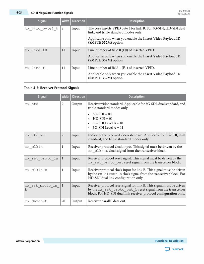
DescriptionDirectionWidthSignal
The core inserts VPID byte 4 for link B. For 3G-SDI, HD-SDI duallink, and triple standard modes only.
Applicable only when you enable the Insert Video Payload ID(SMPTE 352M) option.
Input8tx_vpid_byte4_b
Line number of field 0 (F0) of inserted VPID.
Applicable only when you enable the Insert Video Payload ID(SMPTE 352M) option.
Input11tx_line_f0
Line number of field 1 (F1) of inserted VPID.
Applicable only when you enable the Insert Video Payload ID(SMPTE 352M) option.
Input11tx_line_f1
Table 4-5: Receiver Protocol Signals
DescriptionDirectionWidthSignal
Receiver video standard. Applicable for 3G-SDI, dual standard, andtriple standard modes only.
• SD-SDI = 00• HD-SDI = 01• 3G-SDI Level B = 10• 3G-SDI Level A = 11
Output2rx_std
Indicates the received video standard. Applicable for 3G-SDI, dualstandard, and triple standard modes only.
Input2rx_std_in
Receiver protocol clock input. This signal must be driven by therx_clkout clock signal from the transceiver block.
Input1rx_clkin
Receiver protocol reset signal. This signal must be driven by therx_rst_proto_out reset signal from the transceiver block.
Input1rx_rst_proto_in
Receiver protocol clock input for link B. This signal must be drivenby the rx_clkout_b clock signal from the transceiver block. ForHD-SDI dual link configuration only.
Input1rx_clkin_b
Receiver protocol reset signal for link B. This signal must be drivenby the rx_rst_proto_out_b reset signal from the transceiverblock. For HD-SDI dual link receiver protocol configuration only.
Input1rx_rst_proto_in_b
Receiver parallel data out.Output20rx_dataout
Functional DescriptionAltera Corporation
Feedback
UG-01125SDI II MegaCore Function Signals4-24 2013.06.28
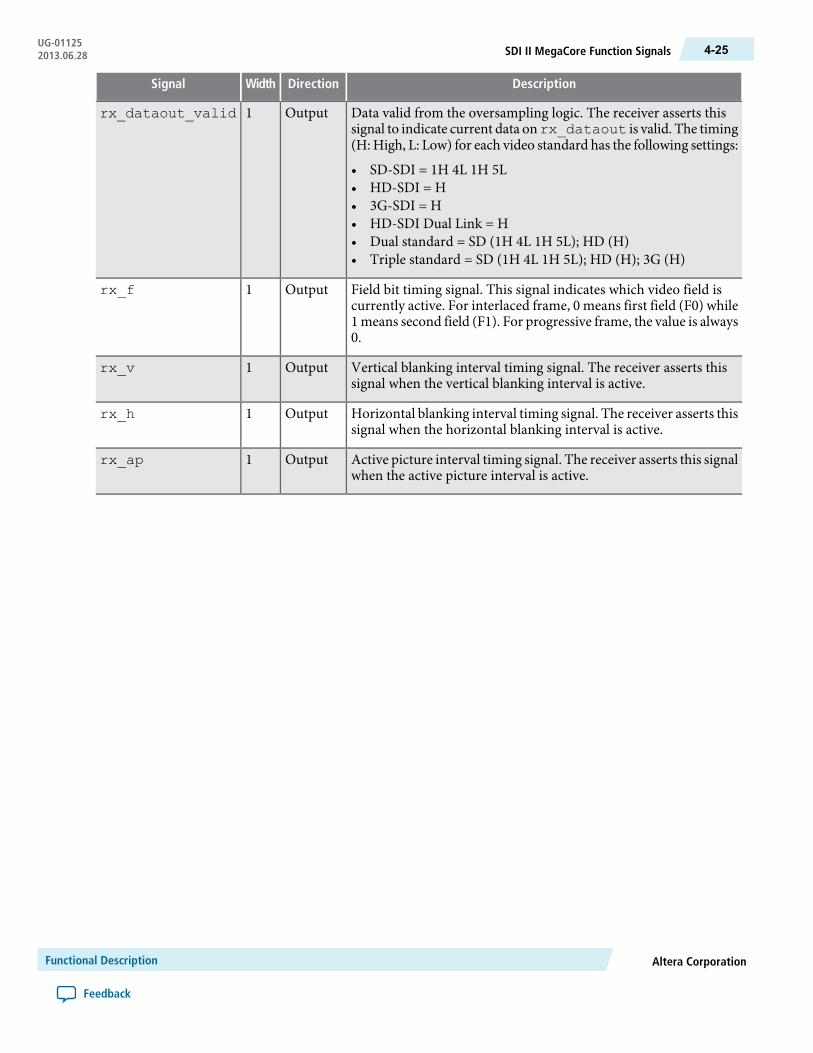
DescriptionDirectionWidthSignal
Data valid from the oversampling logic. The receiver asserts thissignal to indicate current data onrx_dataout is valid. The timing(H:High, L: Low) for each video standard has the following settings:
• SD-SDI = 1H 4L 1H 5L• HD-SDI = H• 3G-SDI = H• HD-SDI Dual Link = H• Dual standard = SD (1H 4L 1H 5L); HD (H)• Triple standard = SD (1H 4L 1H 5L); HD (H); 3G (H)
Output1rx_dataout_valid
Field bit timing signal. This signal indicates which video field iscurrently active. For interlaced frame, 0 means first field (F0) while1means second field (F1). For progressive frame, the value is always0.
Output1rx_f
Vertical blanking interval timing signal. The receiver asserts thissignal when the vertical blanking interval is active.
Output1rx_v
Horizontal blanking interval timing signal. The receiver asserts thissignal when the horizontal blanking interval is active.
Output1rx_h
Active picture interval timing signal. The receiver asserts this signalwhen the active picture interval is active.
Output1rx_ap
Altera CorporationFunctional Description
Feedback
4-25SDI II MegaCore Function SignalsUG-011252013.06.28
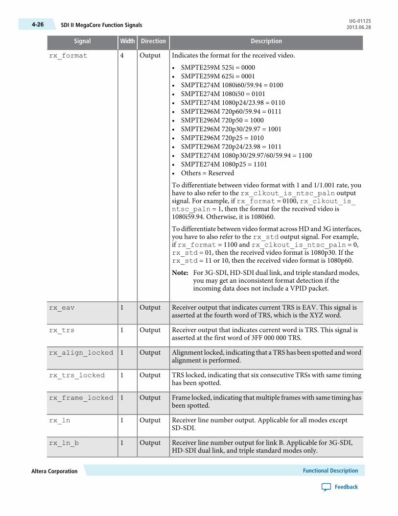
DescriptionDirectionWidthSignal
Indicates the format for the received video.
• SMPTE259M 525i = 0000• SMPTE259M 625i = 0001• SMPTE274M 1080i60/59.94 = 0100• SMPTE274M 1080i50 = 0101• SMPTE274M 1080p24/23.98 = 0110• SMPTE296M 720p60/59.94 = 0111• SMPTE296M 720p50 = 1000• SMPTE296M 720p30/29.97 = 1001• SMPTE296M 720p25 = 1010• SMPTE296M 720p24/23.98 = 1011• SMPTE274M 1080p30/29.97/60/59.94 = 1100• SMPTE274M 1080p25 = 1101• Others = Reserved
To differentiate between video format with 1 and 1/1.001 rate, youhave to also refer to the rx_clkout_is_ntsc_paln outputsignal. For example, if rx_format = 0100, rx_clkout_is_ntsc_paln = 1, then the format for the received video is1080i59.94. Otherwise, it is 1080i60.
To differentiate between video format across HD and 3G interfaces,you have to also refer to the rx_std output signal. For example,if rx_format = 1100 and rx_clkout_is_ntsc_paln = 0,rx_std = 01, then the received video format is 1080p30. If therx_std = 11 or 10, then the received video format is 1080p60.
For 3G-SDI, HD-SDI dual link, and triple standard modes,you may get an inconsistent format detection if theincoming data does not include a VPID packet.
Note:
Output4rx_format
Receiver output that indicates current TRS is EAV. This signal isasserted at the fourth word of TRS, which is the XYZ word.
Output1rx_eav
Receiver output that indicates current word is TRS. This signal isasserted at the first word of 3FF 000 000 TRS.
Output1rx_trs
Alignment locked, indicating that a TRS has been spotted andwordalignment is performed.
Output1rx_align_locked
TRS locked, indicating that six consecutive TRSs with same timinghas been spotted.
Output1rx_trs_locked
Frame locked, indicating that multiple frames with same timing hasbeen spotted.
Output1rx_frame_locked
Receiver line number output. Applicable for all modes exceptSD-SDI.
Output1rx_ln
Receiver line number output for link B. Applicable for 3G-SDI,HD-SDI dual link, and triple standard modes only.
Output1rx_ln_b
Functional DescriptionAltera Corporation
Feedback
UG-01125SDI II MegaCore Function Signals4-26 2013.06.28
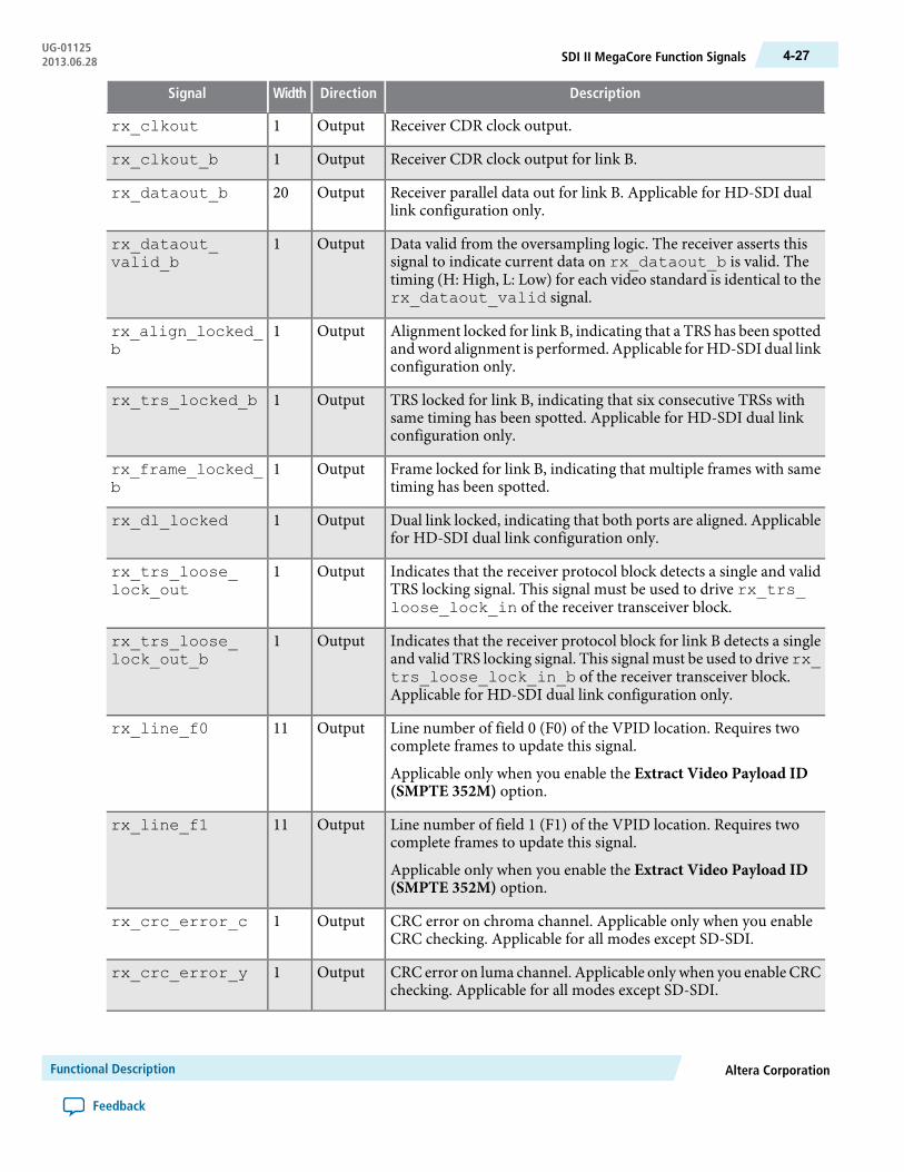
DescriptionDirectionWidthSignal
Receiver CDR clock output.Output1rx_clkout
Receiver CDR clock output for link B.Output1rx_clkout_b
Receiver parallel data out for link B. Applicable for HD-SDI duallink configuration only.
Output20rx_dataout_b
Data valid from the oversampling logic. The receiver asserts thissignal to indicate current data on rx_dataout_b is valid. Thetiming (H: High, L: Low) for each video standard is identical to therx_dataout_valid signal.
Output1rx_dataout_valid_b
Alignment locked for link B, indicating that a TRS has been spottedandword alignment is performed. Applicable forHD-SDI dual linkconfiguration only.
Output1rx_align_locked_b
TRS locked for link B, indicating that six consecutive TRSs withsame timing has been spotted. Applicable for HD-SDI dual linkconfiguration only.
Output1rx_trs_locked_b
Frame locked for link B, indicating that multiple frames with sametiming has been spotted.
Output1rx_frame_locked_b
Dual link locked, indicating that both ports are aligned. Applicablefor HD-SDI dual link configuration only.
Output1rx_dl_locked
Indicates that the receiver protocol block detects a single and validTRS locking signal. This signal must be used to drive rx_trs_loose_lock_in of the receiver transceiver block.
Output1rx_trs_loose_lock_out
Indicates that the receiver protocol block for link B detects a singleand valid TRS locking signal. This signal must be used to driverx_trs_loose_lock_in_b of the receiver transceiver block.Applicable for HD-SDI dual link configuration only.
Output1rx_trs_loose_lock_out_b
Line number of field 0 (F0) of the VPID location. Requires twocomplete frames to update this signal.
Applicable only when you enable the Extract Video Payload ID(SMPTE 352M) option.
Output11rx_line_f0
Line number of field 1 (F1) of the VPID location. Requires twocomplete frames to update this signal.
Applicable only when you enable the Extract Video Payload ID(SMPTE 352M) option.
Output11rx_line_f1
CRC error on chroma channel. Applicable only when you enableCRC checking. Applicable for all modes except SD-SDI.
Output1rx_crc_error_c
CRC error on luma channel. Applicable onlywhen you enable CRCchecking. Applicable for all modes except SD-SDI.
Output1rx_crc_error_y
Altera CorporationFunctional Description
Feedback
4-27SDI II MegaCore Function SignalsUG-011252013.06.28
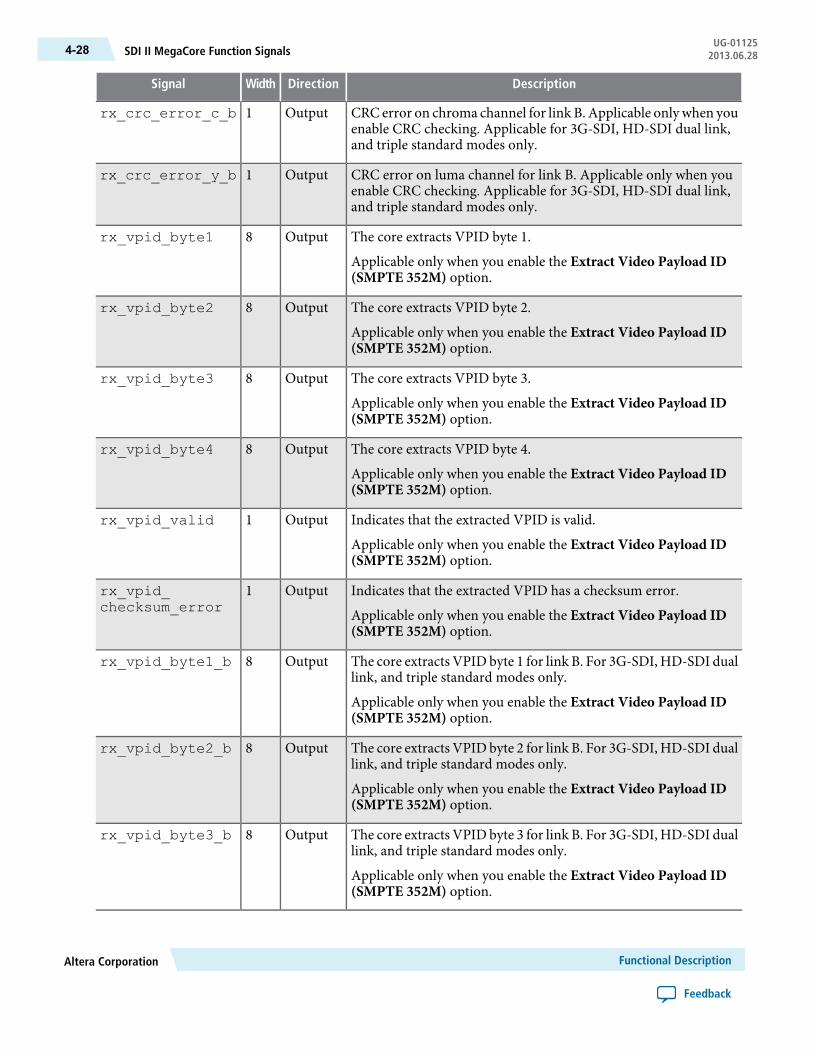
DescriptionDirectionWidthSignal
CRC error on chroma channel for link B. Applicable onlywhen youenable CRC checking. Applicable for 3G-SDI, HD-SDI dual link,and triple standard modes only.
Output1rx_crc_error_c_b
CRC error on luma channel for link B. Applicable only when youenable CRC checking. Applicable for 3G-SDI, HD-SDI dual link,and triple standard modes only.
Output1rx_crc_error_y_b
The core extracts VPID byte 1.
Applicable only when you enable the Extract Video Payload ID(SMPTE 352M) option.
Output8rx_vpid_byte1
The core extracts VPID byte 2.
Applicable only when you enable the Extract Video Payload ID(SMPTE 352M) option.
Output8rx_vpid_byte2
The core extracts VPID byte 3.
Applicable only when you enable the Extract Video Payload ID(SMPTE 352M) option.
Output8rx_vpid_byte3
The core extracts VPID byte 4.
Applicable only when you enable the Extract Video Payload ID(SMPTE 352M) option.
Output8rx_vpid_byte4
Indicates that the extracted VPID is valid.
Applicable only when you enable the Extract Video Payload ID(SMPTE 352M) option.
Output1rx_vpid_valid
Indicates that the extracted VPID has a checksum error.
Applicable only when you enable the Extract Video Payload ID(SMPTE 352M) option.
Output1rx_vpid_checksum_error
The core extracts VPID byte 1 for link B. For 3G-SDI, HD-SDI duallink, and triple standard modes only.
Applicable only when you enable the Extract Video Payload ID(SMPTE 352M) option.
Output8rx_vpid_byte1_b
The core extracts VPID byte 2 for link B. For 3G-SDI, HD-SDI duallink, and triple standard modes only.
Applicable only when you enable the Extract Video Payload ID(SMPTE 352M) option.
Output8rx_vpid_byte2_b
The core extracts VPID byte 3 for link B. For 3G-SDI, HD-SDI duallink, and triple standard modes only.
Applicable only when you enable the Extract Video Payload ID(SMPTE 352M) option.
Output8rx_vpid_byte3_b
Functional DescriptionAltera Corporation
Feedback
UG-01125SDI II MegaCore Function Signals4-28 2013.06.28
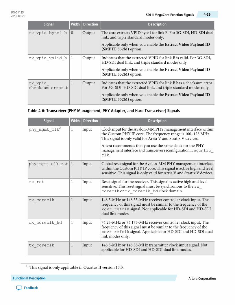
DescriptionDirectionWidthSignal
The core extracts VPID byte 4 for link B. For 3G-SDI, HD-SDI duallink, and triple standard modes only.
Applicable only when you enable the Extract Video Payload ID(SMPTE 352M) option.
Output8rx_vpid_byte4_b
Indicates that the extracted VPID for link B is valid. For 3G-SDI,HD-SDI dual link, and triple standard modes only.
Applicable only when you enable the Extract Video Payload ID(SMPTE 352M) option.
Output1rx_vpid_valid_b
Indicates that the extracted VPID for link B has a checksum error.For 3G-SDI, HD-SDI dual link, and triple standard modes only.
Applicable only when you enable the Extract Video Payload ID(SMPTE 352M) option.
Output1rx_vpid_checksum_error_b
Table 4-6: Transceiver (PHY Management, PHY Adapter, and Hard Transceiver) Signals
DescriptionDirectionWidthSignal
Clock input for theAvalon-MMPHYmanagement interfacewithinthe Custom PHY IP core. The frequency range is 100–125 MHz.This signal is only valid for Arria V and Stratix V devices.
Altera recommends that you use the same clock for the PHYmanagement interface and transceiver reconfiguration,reconfig_clk.
Input1phy_mgmt_clk3
Global reset signal for the Avalon-MM PHY management interfacewithin the Custom PHY IP core. This signal is active high and levelsensitive. This signal is only valid for Arria V and Stratix V devices.
Input1phy_mgmt_clk_rst3
Reset signal for the receiver. This signal is active high and levelsensitive. This reset signal must be synchronous to the rx_coreclk or rx_coreclk_hd clock domain.
Input1rx_rst
148.5-MHz or 148.35-MHz receiver controller clock input. Thefrequency of this signal must be similar to the frequency of thexcvr_refclk signal. Not applicable for HD-SDI and HD-SDIdual link modes.
Input1rx_coreclk
74.25-MHz or 74.175-MHz receiver controller clock input. Thefrequency of this signal must be similar to the frequency of thexcvr_refclk signal. Applicable for HD-SDI and HD-SDI duallink modes only.
Input1rx_coreclk_hd
148.5-MHz or 148.35-MHz transmitter clock input signal. Notapplicable for HD-SDI and HD-SDI dual link modes.
Input1tx_coreclk
3 This signal is only applicable in Quartus II version 13.0.
Altera CorporationFunctional Description
Feedback
4-29SDI II MegaCore Function SignalsUG-011252013.06.28
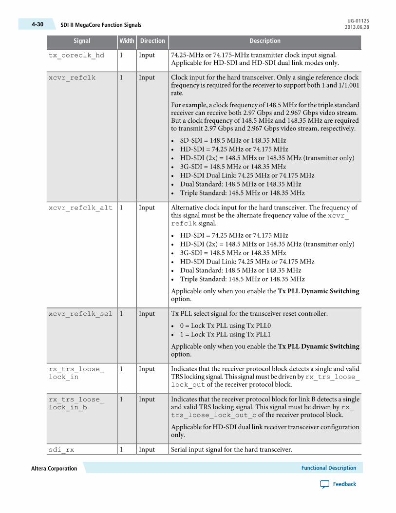
DescriptionDirectionWidthSignal
74.25-MHz or 74.175-MHz transmitter clock input signal.Applicable for HD-SDI and HD-SDI dual link modes only.
Input1tx_coreclk_hd
Clock input for the hard transceiver. Only a single reference clockfrequency is required for the receiver to support both 1 and 1/1.001rate.
For example, a clock frequency of 148.5MHz for the triple standardreceiver can receive both 2.97 Gbps and 2.967 Gbps video stream.But a clock frequency of 148.5 MHz and 148.35 MHz are requiredto transmit 2.97 Gbps and 2.967 Gbps video stream, respectively.
• SD-SDI = 148.5 MHz or 148.35 MHz• HD-SDI = 74.25 MHz or 74.175 MHz• HD-SDI (2x) = 148.5 MHz or 148.35 MHz (transmitter only)• 3G-SDI = 148.5 MHz or 148.35 MHz• HD-SDI Dual Link: 74.25 MHz or 74.175 MHz• Dual Standard: 148.5 MHz or 148.35 MHz• Triple Standard: 148.5 MHz or 148.35 MHz
Input1xcvr_refclk
Alternative clock input for the hard transceiver. The frequency ofthis signal must be the alternate frequency value of the xcvr_refclk signal.
• HD-SDI = 74.25 MHz or 74.175 MHz• HD-SDI (2x) = 148.5 MHz or 148.35 MHz (transmitter only)• 3G-SDI = 148.5 MHz or 148.35 MHz• HD-SDI Dual Link: 74.25 MHz or 74.175 MHz• Dual Standard: 148.5 MHz or 148.35 MHz• Triple Standard: 148.5 MHz or 148.35 MHz
Applicable only when you enable the Tx PLL Dynamic Switchingoption.
Input1xcvr_refclk_alt
Tx PLL select signal for the transceiver reset controller.
• 0 = Lock Tx PLL using Tx PLL0• 1 = Lock Tx PLL using Tx PLL1
Applicable only when you enable the Tx PLL Dynamic Switchingoption.
Input1xcvr_refclk_sel
Indicates that the receiver protocol block detects a single and validTRS locking signal. This signalmust be driven byrx_trs_loose_lock_out of the receiver protocol block.
Input1rx_trs_loose_lock_in
Indicates that the receiver protocol block for link B detects a singleand valid TRS locking signal. This signal must be driven by rx_trs_loose_lock_out_b of the receiver protocol block.
Applicable for HD-SDI dual link receiver transceiver configurationonly.
Input1rx_trs_loose_lock_in_b
Serial input signal for the hard transceiver.Input1sdi_rx
Functional DescriptionAltera Corporation
Feedback
UG-01125SDI II MegaCore Function Signals4-30 2013.06.28
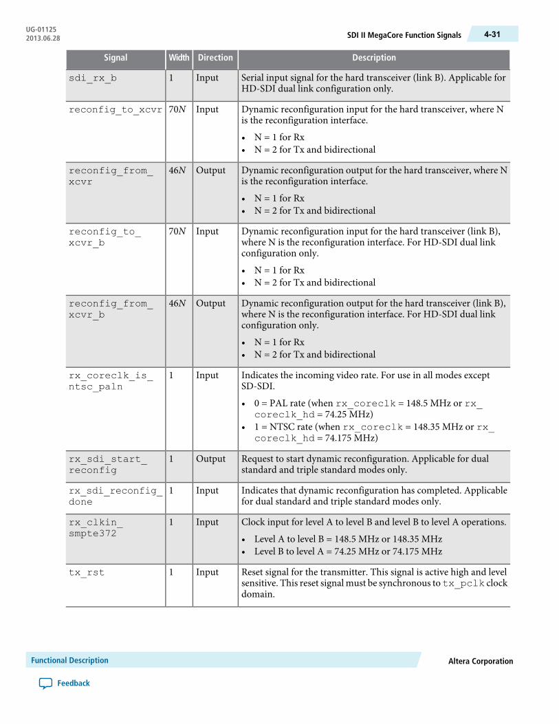
DescriptionDirectionWidthSignal
Serial input signal for the hard transceiver (link B). Applicable forHD-SDI dual link configuration only.
Input1sdi_rx_b
Dynamic reconfiguration input for the hard transceiver, where Nis the reconfiguration interface.
• N = 1 for Rx• N = 2 for Tx and bidirectional
Input70Nreconfig_to_xcvr
Dynamic reconfiguration output for the hard transceiver, where Nis the reconfiguration interface.
• N = 1 for Rx• N = 2 for Tx and bidirectional
Output46Nreconfig_from_xcvr
Dynamic reconfiguration input for the hard transceiver (link B),where N is the reconfiguration interface. For HD-SDI dual linkconfiguration only.
• N = 1 for Rx• N = 2 for Tx and bidirectional
Input70Nreconfig_to_xcvr_b
Dynamic reconfiguration output for the hard transceiver (link B),where N is the reconfiguration interface. For HD-SDI dual linkconfiguration only.
• N = 1 for Rx• N = 2 for Tx and bidirectional
Output46Nreconfig_from_xcvr_b
Indicates the incoming video rate. For use in all modes exceptSD-SDI.
• 0 = PAL rate (when rx_coreclk = 148.5 MHz or rx_coreclk_hd = 74.25 MHz)
• 1 = NTSC rate (when rx_coreclk = 148.35 MHz or rx_coreclk_hd = 74.175 MHz)
Input1rx_coreclk_is_ntsc_paln
Request to start dynamic reconfiguration. Applicable for dualstandard and triple standard modes only.
Output1rx_sdi_start_reconfig
Indicates that dynamic reconfiguration has completed. Applicablefor dual standard and triple standard modes only.
Input1rx_sdi_reconfig_done
Clock input for level A to level B and level B to level A operations.
• Level A to level B = 148.5 MHz or 148.35 MHz• Level B to level A = 74.25 MHz or 74.175 MHz
Input1rx_clkin_smpte372
Reset signal for the transmitter. This signal is active high and levelsensitive. This reset signal must be synchronous totx_pclk clockdomain.
Input1tx_rst
Altera CorporationFunctional Description
Feedback
4-31SDI II MegaCore Function SignalsUG-011252013.06.28
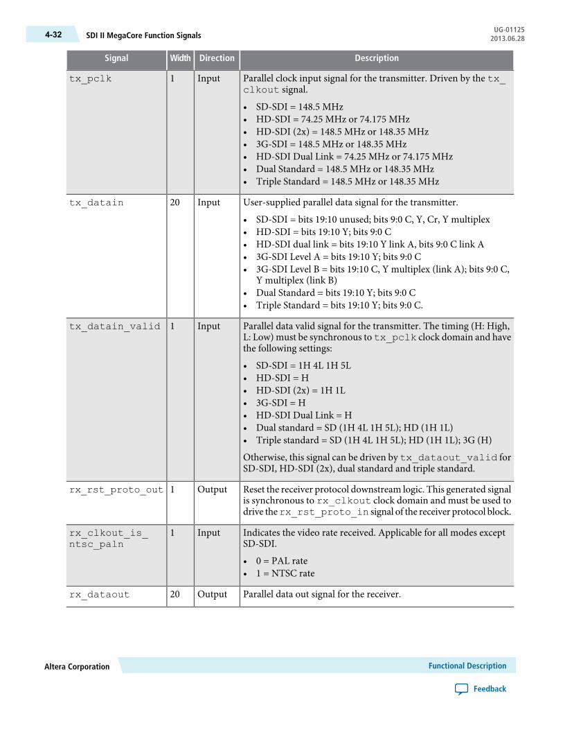
DescriptionDirectionWidthSignal
Parallel clock input signal for the transmitter. Driven by the tx_clkout signal.
• SD-SDI = 148.5 MHz• HD-SDI = 74.25 MHz or 74.175 MHz• HD-SDI (2x) = 148.5 MHz or 148.35 MHz• 3G-SDI = 148.5 MHz or 148.35 MHz• HD-SDI Dual Link = 74.25 MHz or 74.175 MHz• Dual Standard = 148.5 MHz or 148.35 MHz• Triple Standard = 148.5 MHz or 148.35 MHz
Input1tx_pclk
User-supplied parallel data signal for the transmitter.
• SD-SDI = bits 19:10 unused; bits 9:0 C, Y, Cr, Y multiplex• HD-SDI = bits 19:10 Y; bits 9:0 C• HD-SDI dual link = bits 19:10 Y link A, bits 9:0 C link A• 3G-SDI Level A = bits 19:10 Y; bits 9:0 C• 3G-SDI Level B = bits 19:10 C, Y multiplex (link A); bits 9:0 C,
Y multiplex (link B)• Dual Standard = bits 19:10 Y; bits 9:0 C• Triple Standard = bits 19:10 Y; bits 9:0 C.
Input20tx_datain
Parallel data valid signal for the transmitter. The timing (H: High,L: Low) must be synchronous to tx_pclk clock domain and havethe following settings:
• SD-SDI = 1H 4L 1H 5L• HD-SDI = H• HD-SDI (2x) = 1H 1L• 3G-SDI = H• HD-SDI Dual Link = H• Dual standard = SD (1H 4L 1H 5L); HD (1H 1L)• Triple standard = SD (1H 4L 1H 5L); HD (1H 1L); 3G (H)
Otherwise, this signal can be driven by tx_dataout_valid forSD-SDI, HD-SDI (2x), dual standard and triple standard.
Input1tx_datain_valid
Reset the receiver protocol downstream logic. This generated signalis synchronous to rx_clkout clock domain and must be used todrive therx_rst_proto_in signal of the receiver protocol block.
Output1rx_rst_proto_out
Indicates the video rate received. Applicable for all modes exceptSD-SDI.
• 0 = PAL rate• 1 = NTSC rate
Input1rx_clkout_is_ntsc_paln
Parallel data out signal for the receiver.Output20rx_dataout
Functional DescriptionAltera Corporation
Feedback
UG-01125SDI II MegaCore Function Signals4-32 2013.06.28
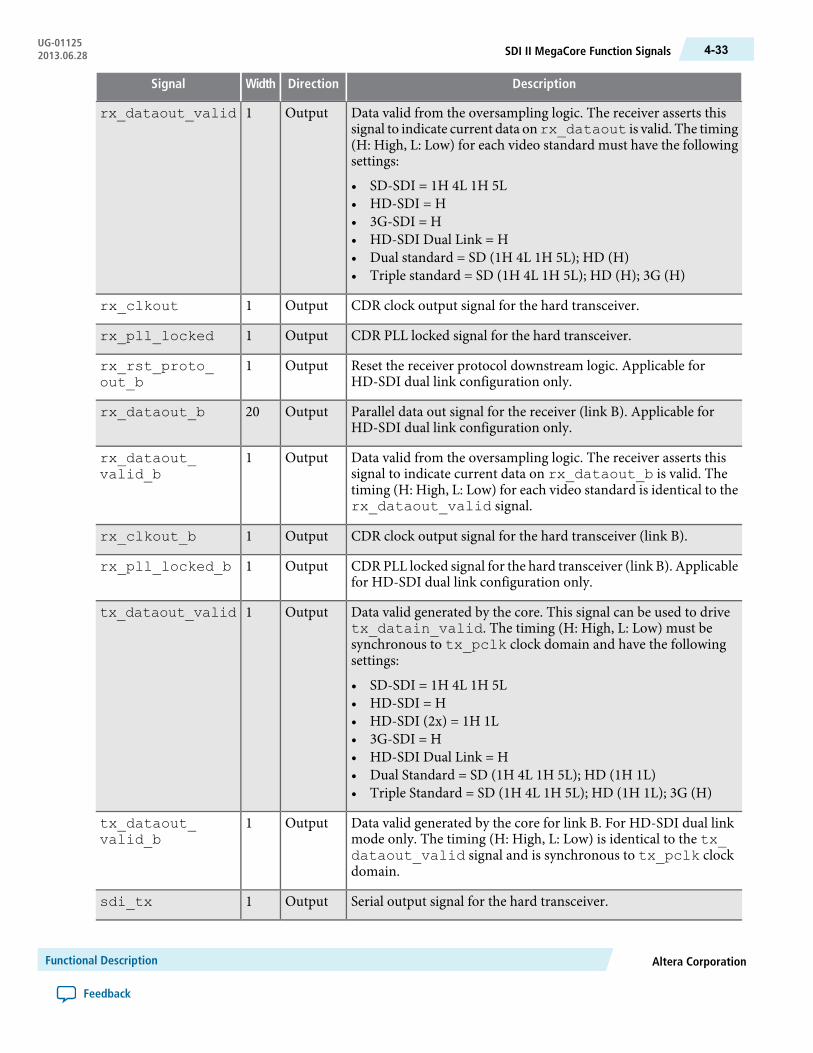
DescriptionDirectionWidthSignal
Data valid from the oversampling logic. The receiver asserts thissignal to indicate current data onrx_dataout is valid. The timing(H: High, L: Low) for each video standard must have the followingsettings:
• SD-SDI = 1H 4L 1H 5L• HD-SDI = H• 3G-SDI = H• HD-SDI Dual Link = H• Dual standard = SD (1H 4L 1H 5L); HD (H)• Triple standard = SD (1H 4L 1H 5L); HD (H); 3G (H)
Output1rx_dataout_valid
CDR clock output signal for the hard transceiver.Output1rx_clkout
CDR PLL locked signal for the hard transceiver.Output1rx_pll_locked
Reset the receiver protocol downstream logic. Applicable forHD-SDI dual link configuration only.
Output1rx_rst_proto_out_b
Parallel data out signal for the receiver (link B). Applicable forHD-SDI dual link configuration only.
Output20rx_dataout_b
Data valid from the oversampling logic. The receiver asserts thissignal to indicate current data on rx_dataout_b is valid. Thetiming (H: High, L: Low) for each video standard is identical to therx_dataout_valid signal.
Output1rx_dataout_valid_b
CDR clock output signal for the hard transceiver (link B).Output1rx_clkout_b
CDR PLL locked signal for the hard transceiver (link B). Applicablefor HD-SDI dual link configuration only.
Output1rx_pll_locked_b
Data valid generated by the core. This signal can be used to drivetx_datain_valid. The timing (H: High, L: Low) must besynchronous to tx_pclk clock domain and have the followingsettings:
• SD-SDI = 1H 4L 1H 5L• HD-SDI = H• HD-SDI (2x) = 1H 1L• 3G-SDI = H• HD-SDI Dual Link = H• Dual Standard = SD (1H 4L 1H 5L); HD (1H 1L)• Triple Standard = SD (1H 4L 1H 5L); HD (1H 1L); 3G (H)
Output1tx_dataout_valid
Data valid generated by the core for link B. For HD-SDI dual linkmode only. The timing (H: High, L: Low) is identical to the tx_dataout_valid signal and is synchronous to tx_pclk clockdomain.
Output1tx_dataout_valid_b
Serial output signal for the hard transceiver.Output1sdi_tx
Altera CorporationFunctional Description
Feedback
4-33SDI II MegaCore Function SignalsUG-011252013.06.28
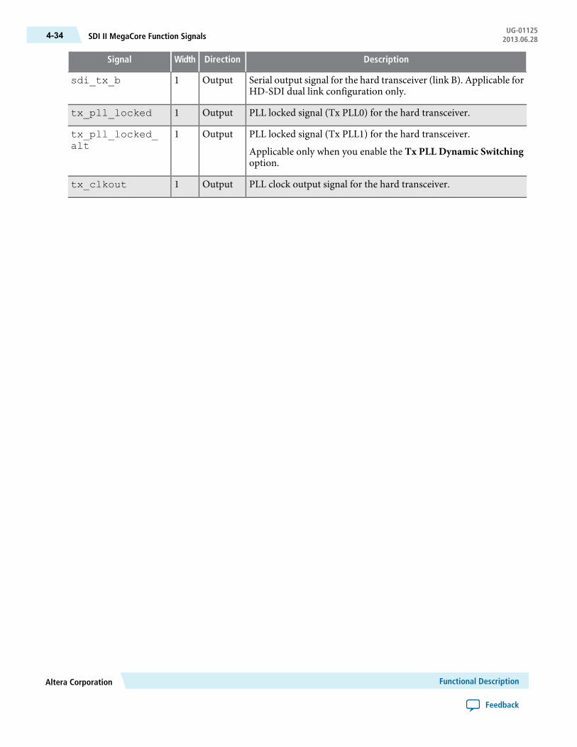
DescriptionDirectionWidthSignal
Serial output signal for the hard transceiver (link B). Applicable forHD-SDI dual link configuration only.
Output1sdi_tx_b
PLL locked signal (Tx PLL0) for the hard transceiver.Output1tx_pll_locked
PLL locked signal (Tx PLL1) for the hard transceiver.
Applicable only when you enable the Tx PLL Dynamic Switchingoption.
Output1tx_pll_locked_alt
PLL clock output signal for the hard transceiver.Output1tx_clkout
Functional DescriptionAltera Corporation
Feedback
UG-01125SDI II MegaCore Function Signals4-34 2013.06.28
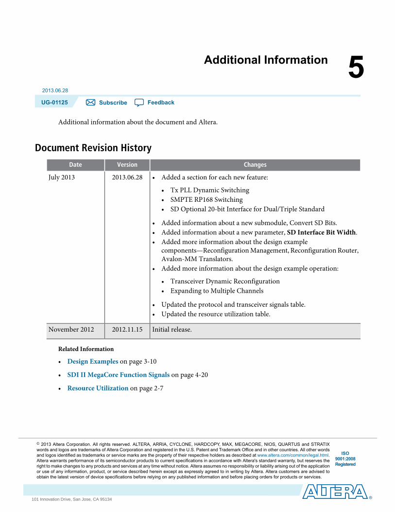
5Additional Information
2013.06.28
UG-01125 Subscribe Feedback
Additional information about the document and Altera.
Document Revision History
ChangesVersionDate
• Added a section for each new feature:
• Tx PLL Dynamic Switching• SMPTE RP168 Switching• SD Optional 20-bit Interface for Dual/Triple Standard
• Added information about a new submodule, Convert SD Bits.• Added information about a new parameter, SD Interface Bit Width.• Added more information about the design example
components—ReconfigurationManagement, ReconfigurationRouter,Avalon-MM Translators.
• Added more information about the design example operation:
• Transceiver Dynamic Reconfiguration• Expanding to Multiple Channels
• Updated the protocol and transceiver signals table.• Updated the resource utilization table.
2013.06.28July 2013
Initial release.2012.11.15November 2012
Related Information
• Design Examples on page 3-10
• SDI II MegaCore Function Signals on page 4-20
• Resource Utilization on page 2-7
ISO9001:2008Registered
© 2013 Altera Corporation. All rights reserved. ALTERA, ARRIA, CYCLONE, HARDCOPY, MAX, MEGACORE, NIOS, QUARTUS and STRATIXwords and logos are trademarks of Altera Corporation and registered in the U.S. Patent and Trademark Office and in other countries. All other wordsand logos identified as trademarks or service marks are the property of their respective holders as described at www.altera.com/common/legal.html.Altera warrants performance of its semiconductor products to current specifications in accordance with Altera's standard warranty, but reserves theright to make changes to any products and services at any time without notice. Altera assumes no responsibility or liability arising out of the applicationor use of any information, product, or service described herein except as expressly agreed to in writing by Altera. Altera customers are advised toobtain the latest version of device specifications before relying on any published information and before placing orders for products or services.
www.altera.com
101 Innovation Drive, San Jose, CA 95134
How to Contact Altera
Table 5-1: Altera Contact Information
AddressContact MethodContact4
www.altera.com/supportWebsiteTechnical support
www.altera.com/trainingWebsiteTechnical training
www.altera.com/literatureWebsiteProduct literature
[email protected] support
[email protected] licensing
Related Information
• www.altera.com/support
• www.altera.com/training
• www.altera.com/literature
4 You can also contact your local Altera sales office or sales representative.
Additional InformationAltera Corporation
Feedback
UG-01125How to Contact Altera5-2 2013.06.28