Embed Size (px)
Citation preview
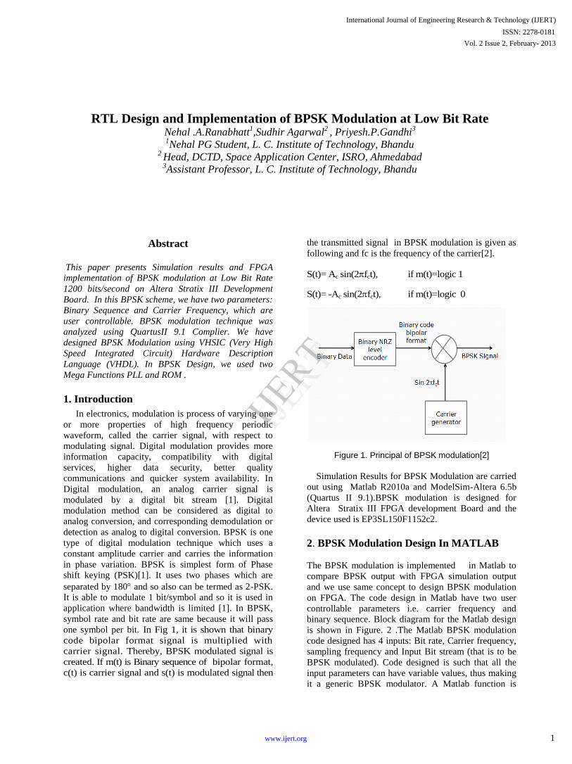
RTL Design and Implementation of BPSK Modulation at Low Bit Rate Nehal .A.Ranabhatt1,Sudhir Agarwal2 , Priyesh.P.Gandhi3 1Nehal PG Student, L. C. Institute of Technology, Bhandu
2 Head, DCTD, Space Application Center, ISRO, Ahmedabad 3Assistant Professor, L. C. Institute of Technology, Bhandu
Abstract
This paper presents Simulation results and FPGA
implementation of BPSK modulation at Low Bit Rate
1200 bits/second on Altera Stratix III Development
Board. In this BPSK scheme, we have two parameters:
Binary Sequence and Carrier Frequency, which are
user controllable. BPSK modulation technique was
analyzed using QuartusII 9.1 Complier. We have
designed BPSK Modulation using VHSIC (Very High
Speed Integrated Circuit) Hardware Description
Language (VHDL). In BPSK Design, we used two
Mega Functions PLL and ROM .
1. Introduction
In electronics, modulation is process of varying one
or more properties of high frequency periodic
waveform, called the carrier signal, with respect to
modulating signal. Digital modulation provides more
information capacity, compatibility with digital
services, higher data security, better quality
communications and quicker system availability. In
Digital modulation, an analog carrier signal is
modulated by a digital bit stream [1]. Digital
modulation method can be considered as digital to
analog conversion, and corresponding demodulation or
detection as analog to digital conversion. BPSK is one
type of digital modulation technique which uses a
constant amplitude carrier and carries the information
in phase variation. BPSK is simplest form of Phase
shift keying (PSK)[1]. It uses two phases which are
separated by 180 and so also can be termed as 2-PSK.
It is able to modulate 1 bit/symbol and so it is used in
application where bandwidth is limited [1]. In BPSK,
symbol rate and bit rate are same because it will pass
one symbol per bit. In Fig 1, it is shown that binary
code bipolar format signal is multiplied with
carrier signal. Thereby, BPSK modulated signal is
created. If m(t) is Binary sequence of bipolar format,
c(t) is carrier signal and s(t) is modulated signal then
the transmitted signal in BPSK modulation is given as
following and fc is the frequency of the carrier[2].
S(t)= Ac sin(2fct), if m(t)=logic 1
S(t)= -Ac sin(2fct), if m(t)=logic 0
Figure 1. Principal of BPSK modulation[2]
Simulation Results for BPSK Modulation are carried
out using Matlab R2010a and ModelSim-Altera 6.5b
(Quartus II 9.1).BPSK modulation is designed for
Altera Stratix III FPGA development Board and the
device used is EP3SL150F1152c2.
2. BPSK Modulation Design In MATLAB
The BPSK modulation is implemented in Matlab to
compare BPSK output with FPGA simulation output
and we use same concept to design BPSK modulation
on FPGA. The code design in Matlab have two user
controllable parameters i.e. carrier frequency and
binary sequence. Block diagram for the Matlab design
is shown in Figure. 2 .The Matlab BPSK modulation
code designed has 4 inputs: Bit rate, Carrier frequency,
sampling frequency and Input Bit stream (that is to be
BPSK modulated). Code designed is such that all the
input parameters can have variable values, thus making
it a generic BPSK modulator. A Matlab function is
International Journal of Engineering Research & Technology (IJERT)
Vol. 2 Issue 2, February- 2013
ISSN: 2278-0181
1www.ijert.org
IJERT
IJERT
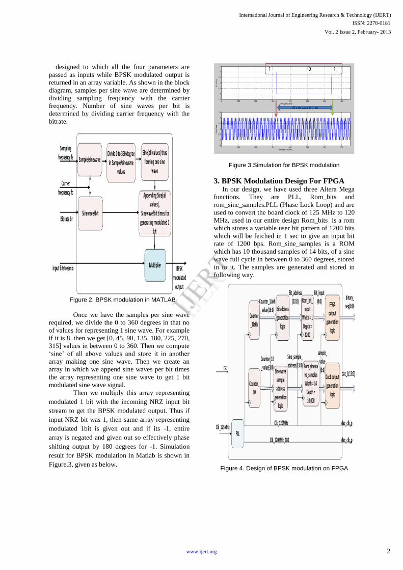
designed to which all the four parameters are
passed as inputs while BPSK modulated output is
returned in an array variable. As shown in the block
diagram, samples per sine wave are determined by
dividing sampling frequency with the carrier
frequency. Number of sine waves per bit is
determined by dividing carrier frequency with the
bitrate.
Figure 2. BPSK modulation in MATLAB
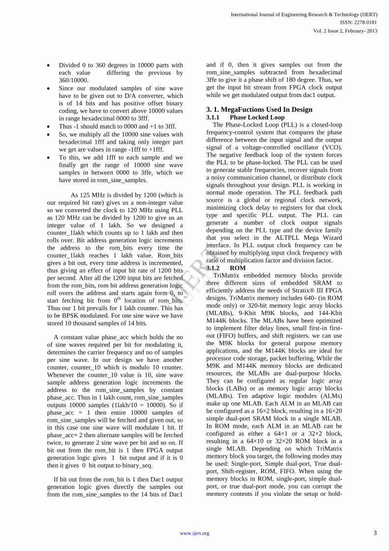
Once we have the samples per sine wave
required, we divide the 0 to 360 degrees in that no
of values for representing 1 sine wave. For example
if it is 8, then we get [0, 45, 90, 135, 180, 225, 270,
315] values in between 0 to 360. Then we compute
„sine‟ of all above values and store it in another
array making one sine wave. Then we create an
array in which we append sine waves per bit times
the array representing one sine wave to get 1 bit
modulated sine wave signal.
Then we multiply this array representing
modulated 1 bit with the incoming NRZ input bit
stream to get the BPSK modulated output. Thus if
input NRZ bit was 1, then same array representing
modulated 1bit is given out and if its -1, entire
array is negated and given out so effectively phase
shifting output by 180 degrees for -1. Simulation
result for BPSK modulation in Matlab is shown in
Figure.3, given as below.
Figure 3.Simulation for BPSK modulation
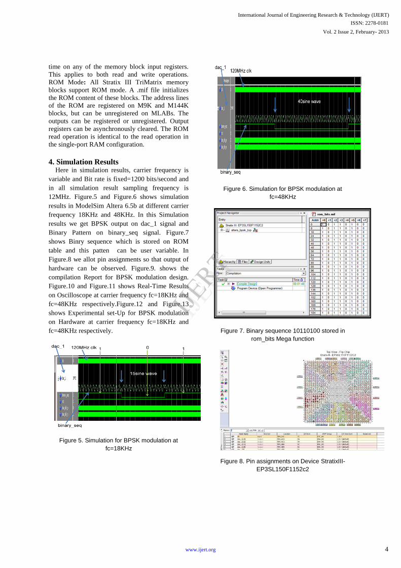
3. BPSK Modulation Design For FPGA In our design, we have used three Altera Mega
functions. They are PLL, Rom_bits and
rom_sine_samples.PLL (Phase Lock Loop) and are
used to convert the board clock of 125 MHz to 120
MHz, used in our entire design Rom_bits is a rom
which stores a variable user bit pattern of 1200 bits
which will be fetched in 1 sec to give an input bit
rate of 1200 bps. Rom_sine_samples is a ROM
which has 10 thousand samples of 14 bits, of a sine
wave full cycle in between 0 to 360 degrees, stored
in to it. The samples are generated and stored in
following way.
Figure 4. Design of BPSK modulation on FPGA
International Journal of Engineering Research & Technology (IJERT)
Vol. 2 Issue 2, February- 2013
ISSN: 2278-0181
2www.ijert.org
IJERT
IJERT
Divided 0 to 360 degrees in 10000 parts with
each value differing the previous by
360/10000.
Since our modulated samples of sine wave
have to be given out to D/A converter, which
is of 14 bits and has positive offset binary
coding, we have to convert above 10000 values
in range hexadecimal 0000 to 3fff.
Thus -1 should match to 0000 and +1 to 3fff.
So, we multiply all the 10000 sine values with
hexadecimal 1fff and taking only integer part
we get are values in range -1fff to +1fff.
To this, we add 1fff to each sample and we
finally get the range of 10000 sine wave
samples in between 0000 to 3ffe, which we
have stored in rom_sine_samples.
As 125 MHz is divided by 1200 (which is
our required bit rate) gives us a non-integer value
so we converted the clock to 120 MHz using PLL
as 120 MHz can be divided by 1200 to give us an
integer value of 1 lakh. So we designed a
counter_1lakh which counts up to 1 lakh and then
rolls over. Bit address generation logic increments
the address to the rom_bits every time the
counter_1lakh reaches 1 lakh value. Rom_bits
gives a bit out, every time address is incremented,
thus giving an effect of input bit rate of 1200 bits
per second. After all the 1200 input bits are fetched
from the rom_bits, rom bit address generation logic
roll overs the address and starts again form 0, to
start fetching bit from 0th
location of rom_bits.
Thus our 1 bit prevails for 1 lakh counter. This has
to be BPSK modulated. For one sine wave we have
stored 10 thousand samples of 14 bits.
A constant value phase_acc which holds the no
of sine waves required per bit for modulating it,
determines the carrier frequency and no of samples
per sine wave. In our design we have another
counter, counter_10 which is modulo 10 counter.
Whenever the counter_10 value is 10, sine wave
sample address generation logic increments the
address to the rom_sine_samples by constant
phase_acc. Thus in 1 lakh count, rom_sine_samples
outputs 10000 samples (1lakh/10 = 10000). So if
phase_acc = 1 then entire 10000 samples of
rom_sine_samples will be fetched and given out, so
in this case one sine wave will modulate 1 bit. If
phase_acc= 2 then alternate samples will be fetched
twice, to generate 2 sine wave per bit and so on. If
bit out from the rom_bit is 1 then FPGA output
generation logic gives 1 bit output and if it is 0
then it gives 0 bit output to binary_seq.
If bit out from the rom_bit is 1 then Dac1 output
generation logic gives directly the samples out
from the rom_sine_samples to the 14 bits of Dac1
and if 0, then it gives samples out from the
rom_sine_samples subtracted from hexadecimal
3ffe to give it a phase shift of 180 degree. Thus, we
get the input bit stream from FPGA clock output
while we get modulated output from dac1 output.
3. 1. MegaFuctions Used In Design 3.1.1 Phase Locked Loop
The Phase-Locked Loop (PLL) is a closed-loop
frequency-control system that compares the phase
difference between the input signal and the output
signal of a voltage-controlled oscillator (VCO).
The negative feedback loop of the system forces
the PLL to be phase-locked. The PLL can be used
to generate stable frequencies, recover signals from
a noisy communication channel, or distribute clock
signals throughout your design. PLL is working in
normal mode operation. The PLL feedback path
source is a global or regional clock network,
minimizing clock delay to registers for that clock
type and specific PLL output. The PLL can
generate a number of clock output signals
depending on the PLL type and the device family
that you select in the ALTPLL Mega Wizard
interface. In PLL output clock frequency can be
obtained by multiplying input clock frequency with
ratio of multiplication factor and division factor.
3.1.2 ROM
TriMatrix embedded memory blocks provide
three different sizes of embedded SRAM to
efficiently address the needs of Stratix® III FPGA
designs. TriMatrix memory includes 640- (in ROM
mode only) or 320-bit memory logic array blocks
(MLABs), 9-Kbit M9K blocks, and 144-Kbit
M144K blocks. The MLABs have been optimized
to implement filter delay lines, small first-in first-
out (FIFO) buffers, and shift registers. we can use
the M9K blocks for general purpose memory
applications, and the M144K blocks are ideal for
processor code storage, packet buffering, While the
M9K and M144K memory blocks are dedicated
resources, the MLABs are dual-purpose blocks.
They can be configured as regular logic array
blocks (LABs) or as memory logic array blocks
(MLABs). Ten adaptive logic modules (ALMs)
make up one MLAB. Each ALM in an MLAB can
be configured as a 16×2 block, resulting in a 16×20
simple dual-port SRAM block in a single MLAB.
In ROM mode, each ALM in an MLAB can be
configured as either a 64×1 or a 32×2 block,
resulting in a 64×10 or 32×20 ROM block in a
single MLAB. Depending on which TriMatrix
memory block you target, the following modes may
be used: Single-port, Simple dual-port, True dual-
port, Shift-register, ROM, FIFO. When using the
memory blocks in ROM, single-port, simple dual-
port, or true dual-port mode, you can corrupt the
memory contents if you violate the setup or hold-
International Journal of Engineering Research & Technology (IJERT)
Vol. 2 Issue 2, February- 2013
ISSN: 2278-0181
3www.ijert.org
IJERT
IJERT
time on any of the memory block input registers.
This applies to both read and write operations.
ROM Mode: All Stratix III TriMatrix memory
blocks support ROM mode. A .mif file initializes
the ROM content of these blocks. The address lines
of the ROM are registered on M9K and M144K
blocks, but can be unregistered on MLABs. The
outputs can be registered or unregistered. Output
registers can be asynchronously cleared. The ROM
read operation is identical to the read operation in
the single-port RAM configuration.
4. Simulation Results Here in simulation results, carrier frequency is
variable and Bit rate is fixed=1200 bits/second and
in all simulation result sampling frequency is
12MHz. Figure.5 and Figure.6 shows simulation
results in ModelSim Altera 6.5b at different carrier
frequency 18KHz and 48KHz. In this Simulation
results we get BPSK output on dac_1 signal and
Binary Pattern on binary_seq signal. Figure.7
shows Binry sequence which is stored on ROM
table and this patten can be user variable. In
Figure.8 we allot pin assignments so that output of
hardware can be observed. Figure.9. shows the
compilation Report for BPSK modulation design.
Figure.10 and Figure.11 shows Real-Time Results
on Oscilloscope at carrier frequency fc=18KHz and
fc=48KHz respectively.Figure.12 and Figure.13
shows Experimental set-Up for BPSK modulation
on Hardware at carrier frequency fc=18KHz and
fc=48KHz respectively.
Figure 5. Simulation for BPSK modulation at
fc=18KHz
Figure 6. Simulation for BPSK modulation at
fc=48KHz
Figure 7. Binary sequence 10110100 stored in
rom_bits Mega function
Figure 8. Pin assignments on Device StratixIII-
EP3SL150F1152c2
International Journal of Engineering Research & Technology (IJERT)
Vol. 2 Issue 2, February- 2013
ISSN: 2278-0181
4www.ijert.org
IJERT
IJERT
Figure 9. Compilation Report
Figure 10. BPSK output on oscilloscope when
fs=12MHz ,fc=18KHz with Bit Pattern 010
Figure 11. BPSK output on oscilloscope when
fs=12MHz ,fc=48KHz with Bit Pattern 01
Figure 12. Experimental set-Up of BPSK Output On
Oscilloscope When fs=12MHz and fc=18KHz with
Bit Pattern 010
Figure 13. Experimental set-Up of BPSK Output On
Oscilloscope When fs=12MHz and fc=48KHz with
Bit Pattern 01
5. Conclusion In FPGA implementation we use
intellectual property. The simplicity of construction
was reached using intellectual property component
in a combination with the VHDL language. In this
paper we implement BPSK modulation on
StratixIII FPGA development Board. In our design
Binary pattern and carrier frequency are variable.
Here we put simulation result for BPSK
modulation in Matlab shown in Fig.3. and
Simulation results in ModelSim Altera shown in
Fig.5 and Fig.6. While designing BPSK modulation
on FPGA we use ROM and PLL Mega Fuctions
provide by Altera. After that we put BPSK output
International Journal of Engineering Research & Technology (IJERT)
Vol. 2 Issue 2, February- 2013
ISSN: 2278-0181
5www.ijert.org
IJERT
IJERT
on Oscilloscope with Different carrier frequency
fc=18KHz shown in Fig.10 and , fc=48KHz shown
in Fig. 11and finally we put photographs of BPSK
modulation on hard ware at 1200 bps Bit rate
shown in Fig 12 and Fig 13. In BPSK modulator,
for 0 bit, it is shown that processing data is samples
of delayed carrier signal (180 degrees of phase
delay), for 1 symbol, it is shown that processing
data is samples of carrier signal.
6. References [1] C. Erdoğan, I. Myderrizi, and S. Minaei “FPGA
Implementation of BASK-BFSK-BPSK Digital Modulators” IEEE Antennas and Propagation Magazine, Vol. 54, No. 2, April 2012.
[2] Mehmet Sonmez and Ayhan Akbal “FPGA-Based BASK and BPSK Modulators Using VHDL: Design, Applications and Performance Comparison for Different Modulator Algorithms” In March 2012, International Journal of Computer Applications (0975 – 8887) Volume 42– No.13, March 2012.
[3] ] S.O.Popescu and A.S. Gontean “Performance comparison of the BPSK and QPSK Modulation Techniques on FPGA” 17th International Symposium for Design and Technology in Electronic Packaging (SIITME) 2011 IEEE .
[4] S.O. Popescu, A.S.Gontean and G.Budura “BPSK System on Spartan 3E FPGA” SAMI 2012 • 10th IEEE Jubilee International Symposium on Applied Machine Intelligence and Informatics • January 26-28, 2012.
[5] Michal Kováč “BPSK, QPSK MODULATOR Simulation Model”VUT Faculty of electrical engineering and communication, 2006. 82 s.
[6] S.O. Popescu, A.S.Gontean and G.Budura “Simulation and Implementation of a BPSK Modulator on FPGA ”6th IEEE International Symposium on Applied Computational Intelligence and Informatics • May 19–21, 2011.
[7] Manoj Kollam1, S.A.S.Krishna Chaithanya2, Nagaraju kommu3 “Design And Implementation Of An Enhanced DDs Based Digital Modulator For Multiple Modulation Schemes” International Journal of Smart Sensors and Ad Hoc Networks (IJSSAN) Volume-1, Issue-1, 2011.
[8] Satish Sharma ,Sunil, Vijaykumar Pujari, Vanitha M, P.Lakshminarsimhan.FPGA Implementation of M-PSK Modulators for Satellite Communication, International Conference on Advances in Recent Technologies in Communication and Computing 2010.
[9] Philippe Dondon- J.M Micouleau- J. Legall-P.Kadionik Design of a low cost BPSK modulator/demodulator for a practical teaching of digital modulation techniques Author manuscript, published in "Engineering Education, Agios Nicholaos : Greece 2007.
[10] Wenmiao Song and Qiongqiong Yao esign and Implement of QPSK Modem Based on FPGA IEEE ,2010.
[11] ]http://www.altera.com/devices/fpga/stratix-fpgas/stratix-iii/overview/st3-overview.html
[12] http://www.altera.com/devices/fpga/stratix-fpgas/stratix iii/overview/architecture/st3- dsp.html
[13] http://www.altera.com/devices/fpga/stratix-fpgas/stratix-iii/overview/power/st3-power.html-video
International Journal of Engineering Research & Technology (IJERT)
Vol. 2 Issue 2, February- 2013
ISSN: 2278-0181
6www.ijert.org
IJERT
IJERT