Embed Size (px)
Citation preview
8/11/2019 Rogers 537 CH04
http://slidepdf.com/reader/full/rogers-537-ch04 1/30
129
C H A P T E R 4
System-Level Architecture
4.1 Introduction
In this chapter, various configurations of circuit building blocks used to form radiosare discussed. Some of the following sections deal with block diagrams for completetransceivers, while other sections are about subsystems that solve particular prob-lems. Although it would be impossible to discuss all architectures here, common
ones are presented and such discussion includes many of the basic concepts com-mon to most architectures.
4.2 Superheterodyne Transceivers
A block diagram of a typical half duplex superheterodyne radio transceiver isshown in Figure 4.1 [1–7]. Modulated signals are transmitted and received at somefrequency by an antenna. If the radio is receiving information, then the signals arepassed from the antenna to the receiver (Rx) part of the radio. If the radio is trans-mitting, then signals are passed to the antenna from the transmitter (Tx) part of
the radio. Radios either transmit and receive at the same time (called a full-duplextransceiver) or alternate between transmitting and receiving (called a half-duplextransceiver). In a half-duplex transceiver, it is possible to put a switch between theantenna and the Rx and Tx paths to provide improved isolation, while in a full-duplex transceiver, the switch must be omitted and the two input filters (usuallycalled a duplexor) have the sole responsibility of isolating the Tx and Rx pathswithout the aid of a switch.
In the Rx path, the signals are first passed through a preselect bandpass filter toremove interference from frequency bands other than the one of interest. Althoughthe preselect BPF will negatively impact the noise figure of the radio, placing a filterhere makes the design of the receiver input easier as it will reduce the power levelswith which the front end must deal. The signal is then amplified by a low noiseamplifier (LNA) to increase the power in weak signals, while adding as little noise(unwanted random signals) as possible. This amplifier may include some form ofadjustable gain or gain steps. Adding a gain step here complicates the design of theLNA, but allows the gain to be reduced for larger input levels, thus reducing the lin-earity requirements of the rest of the radio. The spectrum is then further filtered byan image filter. This is required because the preselect BPF will typically not provideenough image rejection, or may have been omitted for noise reasons. The signalis then downconverted by a mixer to an intermediate frequency (IF). The IF fre-quency must be chosen with great care, taking into account many factors including
ART_Rogers_Ch04.indd 129 Manila Typesetting Company 08/23/2013
8/11/2019 Rogers 537 CH04
http://slidepdf.com/reader/full/rogers-537-ch04 2/30
130 System-Level Architecture
interaction of spurs and mixing of LO harmonics. Generally, a higher IF frequencywill make the job of the image filter easier, while making the design of the IF stageand especially the IF filter harder as it will need to work at a higher frequency.
The mixer (also sometimes called a multiplier) mixes the incoming radio- frequency (RF) signal with the output from the RF frequency synthesizer which isan accurate frequency reference generator also called a local oscillator (LO). TheLO is tuned so that the frequency of the desired IF signal is always at the same
frequency. The LO can be either low-side injected (the LO is at a frequency less thanthe RF frequency) or high-side injected (the LO is at a frequency greater than the RFfrequency). For low-side injection, the IF frequency is given by
= -IF RF LOf f f (4.1)
while for high-side injection it is
= -IF LO RFf f f (4.2)
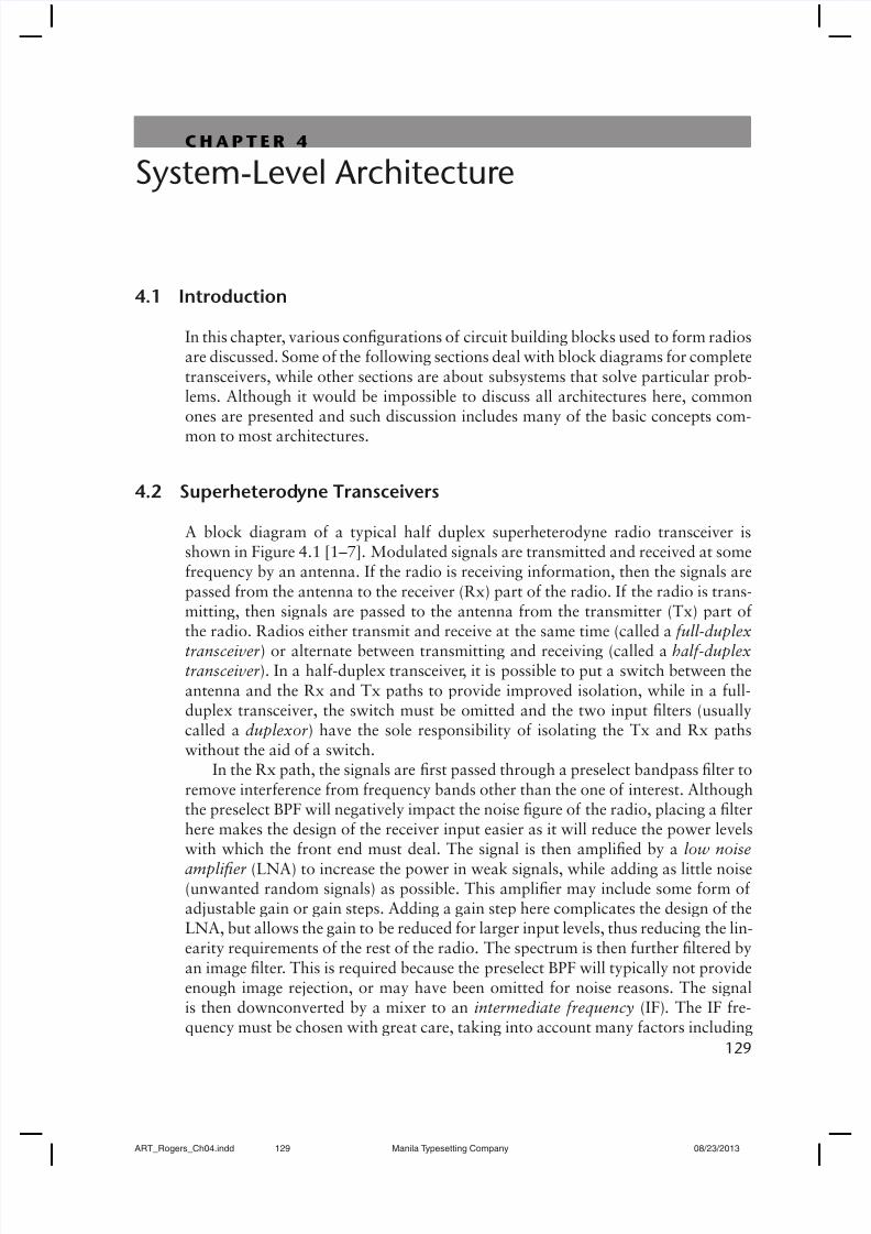
As the IF stage is usually at a fixed frequency, the synthesizer must be program-mable so that it can be tuned to whatever input frequency is desired at a given time.An input signal at an equal distance from the LO on the other side from the desiredRF signal is called the image signal . It is called the image because a signal at thisfrequency after mixing will be at the same IF as the desired signal. Therefore, theimage signal cannot be removed by filtering after mixing has taken place. Thus, animportant job of the RF filters is to remove any image signals before such mixingaction takes place. This is illustrated in Figure 4.2. It is also important to keep anyLO spurs as low as possible. For example, in Figure 4.2, the LO spurs illustratedwill act to convert channels 2 and 6 into the IF frequency band. If these spurs aretoo strong, then this can corrupt the downconversion process as well. Also, aftermixing, there is no further filtering that can fix this problem.
ImageFilter Mixer
Power Amp
LNA
PreselectBPF
SwitchRx
Tx
AGCIFFilter
AGCIFFilter
RFSynthesizer
IQ DemodBBFilters
BBFilters
IFSynthesizer
To DSP
From DSP
Antenna
90°
A/D
D/A
Mixer Driver
AGC
AGC
LO1
LO1
LO2_I
LO2_I
LO2_Q
LO2_Q
I_Rx
Q_Rx
I_Tx
Q_Tx
SBR
Figure 4.1 A typical half-duplex superheterodyne radio transceiver.
ART_Rogers_Ch04.indd 130 Manila Typesetting Company 08/23/2013
8/11/2019 Rogers 537 CH04
http://slidepdf.com/reader/full/rogers-537-ch04 3/30
4.2 Superheterodyne Transceivers 131
After mixing to an IF, additional filtering is usually performed. At the IF, un-wanted channels can be filtered out as now the desired channel is always centeredat the same known frequency, leaving only the channel of interest now centered atthe IF, and possibly some subset of the original adjacent channels depending on thequality of the filter used. Usually, automatic gain control (AGC) amplifiers are alsoincluded at the IF. They adjust the gain of the radio so that its output amplitude isalways constant. AGC is performed at the IF to avoid mismatches in gain betweenthe I and Q paths once the signal reaches baseband. Once through the AGC, thesignals are downconverted a second time to baseband (the signals are now centeredaround DC or zero frequency). This second downconversion requires a second fre-quency synthesizer that produces both 0° and 90° output signals at the IF frequency.
Two mixers downconvert the signals into in-phase (I) and quadrature phase (Q)paths. By using two separate paths, both amplitude and phase information can berecovered, and as a result, the incoming phase of the RF signal does not need tobe synchronized to the phase of the LO tone. The I and Q signals are then passedthrough baseband filters which remove the rest of the unwanted channels. Finally,the signal is passed through an analog-to-digital converter and into the back endof the radio. There may be additional, possibly programmable, gain stages in thebaseband. The better the quality of baseband filter the easier the job of the ADCas a good quality BB filter will remove more unwanted out-of-band energy than apoor quality one. Thus, there is a direct tradeoff between the performance levelsof these two components. Further signal processing is performed in the basebandsignal processing (BBSP) circuitry in the back end of the radio.
The transmitter works much the same way except in reverse. The BBSP circuitryfollowed by the digital-to-analog converters (DAC) produces signals in quadrature.These signals are then filtered (presumably the spectrum of the signals has alreadybeen shaped in the BBSP section of the radio, but harmonics or other unwantedtones can be generated by the DAC) and upconverted to an IF frequency where theyare summed into one signal. The Tx will usually have some AGC function whichmay be either in the baseband or the IF stage. Placing AGC in the baseband createsmatching issues, while implementing it at higher frequencies will make the circuitimplementation harder. The IF signal is upconverted to the RF frequency by the
Frequency
1 2 3 4 5 6 7 8
LO1
RF Filter
f IF
1 23
4
56 7 8
f IF
f IF
Evil
ImageTone
LO2
IF Filter
LO
Spur
LO
Spur
3 4 5
BB Fil ter
f IF
Radio Channels
Figure 4.2 Figure showing radio receiver frequency plan. As shown, the radio is tuned to receivechannel 4 and has a low-side injected LO.
ART_Rogers_Ch04.indd 131 Manila Typesetting Company 08/23/2013
8/11/2019 Rogers 537 CH04
http://slidepdf.com/reader/full/rogers-537-ch04 4/30
132 System-Level Architecture
mixer. If the LO is low-side injected the mixer is used to generate sum, rather thandifference products. Thus, for low-side injection, the RF frequency is given by
= +RF LO IFf f f (4.3)
and if the LO is high-side injected, the frequency of the RF signal is given by
= -RF LO IFf f f (4.4)
Note that the mixer in either case will create an unwanted sideband as both thesum and difference frequencies will be generated, regardless of which one is actu-ally wanted. Once upconverted to RF, the signal is passed through a sideband selectfilter (SBS) to remove the unwanted sideband and any LO feed through as well. Ide-ally, this is done before the PA to avoid using power to amplify an unwanted signal.A power amplifier is next used to increase the power of the signals. After the PA,
additional filters may be present to remove PA harmonics and make sure that trans-mit power masks are not violated (transmit power masks specify the maximumallowed radiated power outside the desired channel bandwidth). The RF signal isthen radiated by the antenna into the air. In the RF section, the PA itself may havea power control function or additional AGC. If the power level is constant, it mustbe high enough so that the signal can be detected at the maximum distance dictatedby the system specifications.
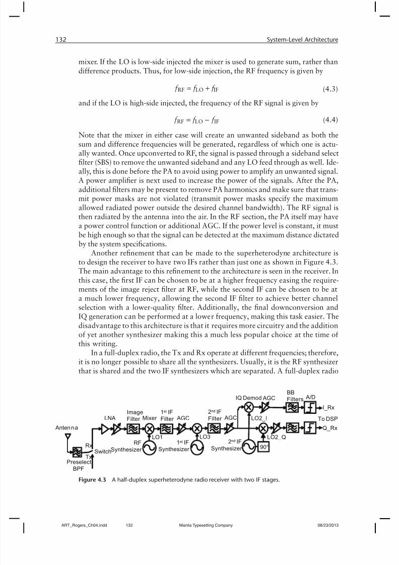
Another refinement that can be made to the superheterodyne architecture isto design the receiver to have two IFs rather than just one as shown in Figure 4.3.The main advantage to this refinement to the architecture is seen in the receiver. Inthis case, the first IF can be chosen to be at a higher frequency easing the require-
ments of the image reject filter at RF, while the second IF can be chosen to be ata much lower frequency, allowing the second IF filter to achieve better channelselection with a lower-quality filter. Additionally, the final downconversion andIQ generation can be performed at a lower frequency, making this task easier. Thedisadvantage to this architecture is that it requires more circuitry and the additionof yet another synthesizer making this a much less popular choice at the time ofthis writing.
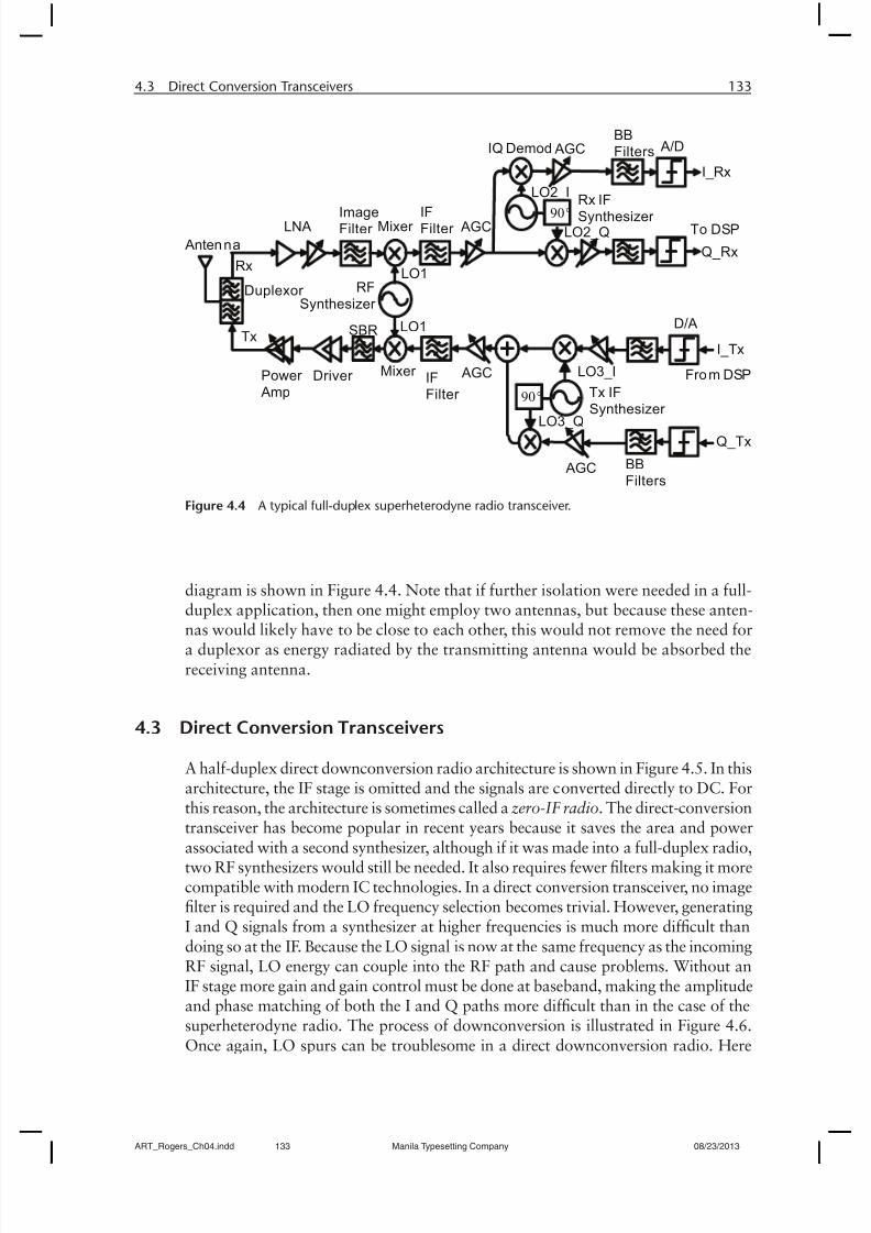
In a full-duplex radio, the Tx and Rx operate at different frequencies; therefore,it is no longer possible to share all the synthesizers. Usually, it is the RF synthesizerthat is shared and the two IF synthesizers which are separated. A full-duplex radio
Image
Filter Mixer LNA
Preselect
BPF
SwitchRx
Tx
AGC2nd IF
Filter
RF
Synthesizer
IQ DemodBB
Filters
2nd IF
Synthesizer
To DSP
Antenna
A/D AGC
LO1
LO2_I
LO2_Q
I_Rx
Q_Rx
AGC1st IF
Filter
1st IF
Synthesizer
LO3
90°
Figure 4.3 A half-duplex superheterodyne radio receiver with two IF stages.
ART_Rogers_Ch04.indd 132 Manila Typesetting Company 08/23/2013
8/11/2019 Rogers 537 CH04
http://slidepdf.com/reader/full/rogers-537-ch04 5/30
4.3 Direct Conversion Transceivers 133
diagram is shown in Figure 4.4. Note that if further isolation were needed in a full-duplex application, then one might employ two antennas, but because these anten-
nas would likely have to be close to each other, this would not remove the need fora duplexor as energy radiated by the transmitting antenna would be absorbed thereceiving antenna.
4.3 Direct Conversion Transceivers
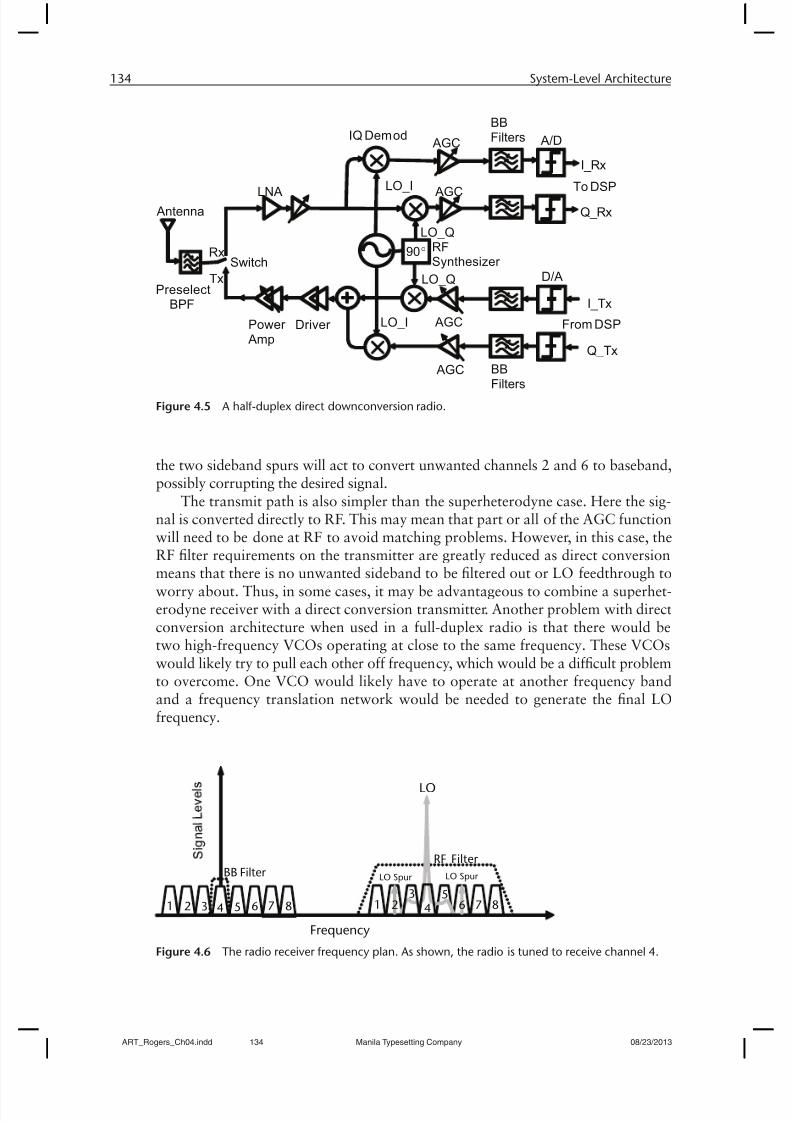
A half-duplex direct downconversion radio architecture is shown in Figure 4.5. In thisarchitecture, the IF stage is omitted and the signals are converted directly to DC. Forthis reason, the architecture is sometimes called a zero-IF radio. The direct-conversiontransceiver has become popular in recent years because it saves the area and powerassociated with a second synthesizer, although if it was made into a full-duplex radio,two RF synthesizers would still be needed. It also requires fewer filters making it morecompatible with modern IC technologies. In a direct conversion transceiver, no imagefilter is required and the LO frequency selection becomes trivial. However, generatingI and Q signals from a synthesizer at higher frequencies is much more difficult thandoing so at the IF. Because the LO signal is now at the same frequency as the incomingRF signal, LO energy can couple into the RF path and cause problems. Without anIF stage more gain and gain control must be done at baseband, making the amplitudeand phase matching of both the I and Q paths more difficult than in the case of thesuperheterodyne radio. The process of downconversion is illustrated in Figure 4.6.
Once again, LO spurs can be troublesome in a direct downconversion radio. Here
ImageFilter Mixer
Power
Amp
LNA
Duplexor
Rx
Tx
AGCIFFilter
AGCIF
Filter
RF
Synthesizer
IQ DemodBB
Filters
BB
Filters
Rx IF
Synthesizer To DSP
From DSP
Antenna
90°
A/D
D/A
Mixer Driver
AGC
AGC
LO1
LO1
LO2_I
LO3_I
LO2_Q
LO3_Q
I_Rx
Q_Rx
I_Tx
Q_Tx
90° Tx IF
Synthesizer
SBR
Figure 4.4 A typical full-duplex superheterodyne radio transceiver.
ART_Rogers_Ch04.indd 133 Manila Typesetting Company 08/23/2013
8/11/2019 Rogers 537 CH04
http://slidepdf.com/reader/full/rogers-537-ch04 6/30
8/11/2019 Rogers 537 CH04
http://slidepdf.com/reader/full/rogers-537-ch04 7/30
4.4 Offset Phase Locked Loop (PLL) Transmitters 135
4.4 Offset Phase Locked Loop (PLL) Transmitters
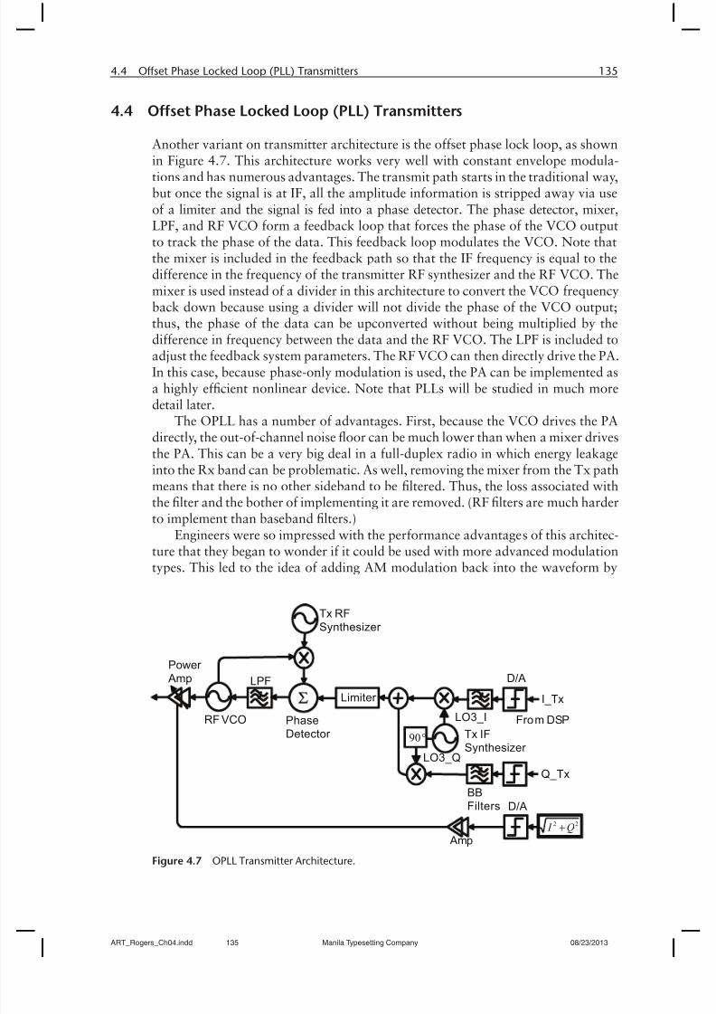
Another variant on transmitter architecture is the offset phase lock loop, as shownin Figure 4.7. This architecture works very well with constant envelope modula-
tions and has numerous advantages. The transmit path starts in the traditional way,but once the signal is at IF, all the amplitude information is stripped away via useof a limiter and the signal is fed into a phase detector. The phase detector, mixer,LPF, and RF VCO form a feedback loop that forces the phase of the VCO outputto track the phase of the data. This feedback loop modulates the VCO. Note thatthe mixer is included in the feedback path so that the IF frequency is equal to thedifference in the frequency of the transmitter RF synthesizer and the RF VCO. Themixer is used instead of a divider in this architecture to convert the VCO frequencyback down because using a divider will not divide the phase of the VCO output;thus, the phase of the data can be upconverted without being multiplied by the
difference in frequency between the data and the RF VCO. The LPF is included toadjust the feedback system parameters. The RF VCO can then directly drive the PA.In this case, because phase-only modulation is used, the PA can be implemented asa highly efficient nonlinear device. Note that PLLs will be studied in much moredetail later.
The OPLL has a number of advantages. First, because the VCO drives the PAdirectly, the out-of-channel noise floor can be much lower than when a mixer drivesthe PA. This can be a very big deal in a full-duplex radio in which energy leakageinto the Rx band can be problematic. As well, removing the mixer from the Tx pathmeans that there is no other sideband to be filtered. Thus, the loss associated withthe filter and the bother of implementing it are removed. (RF filters are much harder
to implement than baseband filters.)Engineers were so impressed with the performance advantages of this architec-
ture that they began to wonder if it could be used with more advanced modulationtypes. This led to the idea of adding AM modulation back into the waveform by
Power
Amp
RF VCO
BB
Filters
From DSP
D/ALPF
LO3_I
LO3_Q
I_Tx
Q_Tx
90° Tx IF
Synthesizer
Limiter
Tx RF
Synthesizer
Phase
Detector
22Q I +
Amp
D/A
Figure 4.7 OPLL Transmitter Architecture.
ART_Rogers_Ch04.indd 135 Manila Typesetting Company 08/23/2013
8/11/2019 Rogers 537 CH04
http://slidepdf.com/reader/full/rogers-537-ch04 8/30
136 System-Level Architecture
dynamically adjusting the power supply of the PA. This is done from the base-band by taking the modulation amplitude, passing it through a digital-to-analogconverter, amplifying it, and applying the signal to the PA. In addition to all theadvantages previously discussed, it is now also possible to have AM modulation on
top of a phase modulated signal with a highly efficient nonlinear PA.
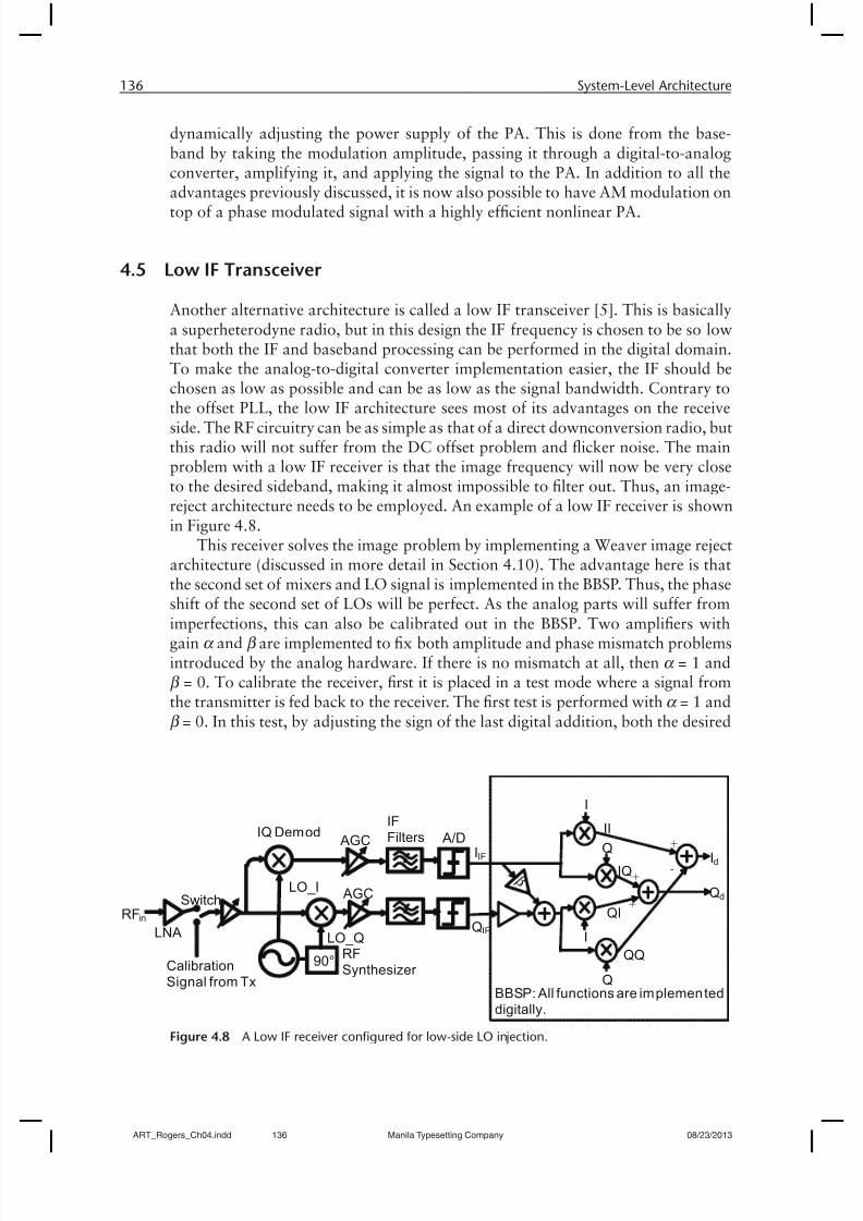
4.5 Low IF Transceiver
Another alternative architecture is called a low IF transceiver [5]. This is basicallya superheterodyne radio, but in this design the IF frequency is chosen to be so lowthat both the IF and baseband processing can be performed in the digital domain.To make the analog-to-digital converter implementation easier, the IF should bechosen as low as possible and can be as low as the signal bandwidth. Contrary to
the offset PLL, the low IF architecture sees most of its advantages on the receiveside. The RF circuitry can be as simple as that of a direct downconversion radio, butthis radio will not suffer from the DC offset problem and flicker noise. The mainproblem with a low IF receiver is that the image frequency will now be very closeto the desired sideband, making it almost impossible to filter out. Thus, an image-reject architecture needs to be employed. An example of a low IF receiver is shownin Figure 4.8.
This receiver solves the image problem by implementing a Weaver image rejectarchitecture (discussed in more detail in Section 4.10). The advantage here is thatthe second set of mixers and LO signal is implemented in the BBSP. Thus, the phaseshift of the second set of LOs will be perfect. As the analog parts will suffer from
imperfections, this can also be calibrated out in the BBSP. Two amplifiers withgain α and β are implemented to fix both amplitude and phase mismatch problemsintroduced by the analog hardware. If there is no mismatch at all, then α = 1 andβ = 0. To calibrate the receiver, first it is placed in a test mode where a signal fromthe transmitter is fed back to the receiver. The first test is performed with α = 1 andβ = 0. In this test, by adjusting the sign of the last digital addition, both the desired
IQ DemodIFFilters
RFSynthesizer
90°
AGC
AGC A/D
LNA
RFin
LO_I
LO_Q
IIF
QIF
BBSP: All functions are implementeddigitally.
Q
Q
I
I
+
-+
+
II
IQ
QI
Id
QdSwitch
CalibrationSignal from Tx
Figure 4.8 A Low IF receiver configured for low-side LO injection.
ART_Rogers_Ch04.indd 136 Manila Typesetting Company 08/23/2013
8/11/2019 Rogers 537 CH04
http://slidepdf.com/reader/full/rogers-537-ch04 9/30
4.5 Low IF Transceiver 137
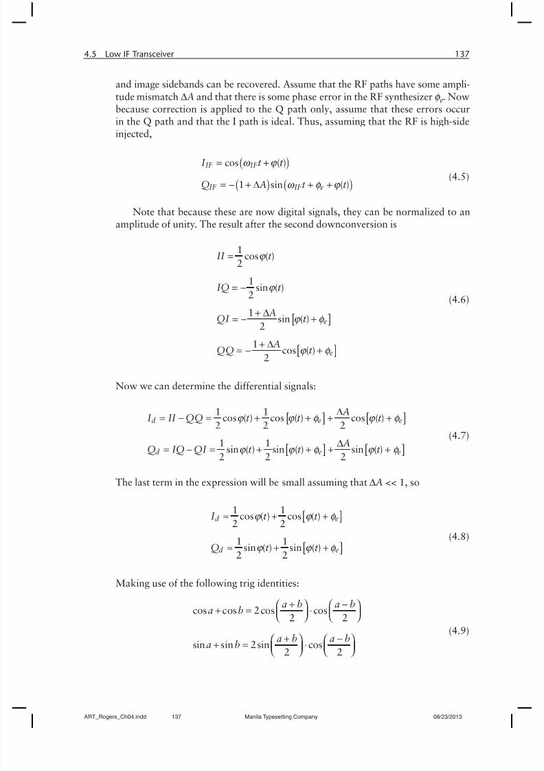
and image sidebands can be recovered. Assume that the RF paths have some ampli-tude mismatch DA and that there is some phase error in the RF synthesizer φ e. Nowbecause correction is applied to the Q path only, assume that these errors occurin the Q path and that the I path is ideal. Thus, assuming that the RF is high-side
injected,
( )
( ) ( )
cos ( )
1 sin ( )
IF IF
IF IF e
I t t
Q A t t
ω ϕ
ω φ ϕ
= +
= - + D + + (4.5)
Note that because these are now digital signals, they can be normalized to anamplitude of unity. The result after the second downconversion is
[ ]
[ ]
1cos ( )
2
1sin ( )
2
1sin ( )
2
1cos ( )
2
e
e
II t
IQ t
AQI t
AQQ t
ϕ
ϕ
ϕ φ
ϕ φ
=
= -
+ D= - +
+ D= - +
(4.6)
Now we can determine the differential signals:
[ ] [ ]
[ ] [ ]
1 1cos ( ) cos ( ) cos ( )
1 1sin ( ) sin ( ) sin ( )
AI II QQ t t t
A
D
D
2 2 2
2 2 2
d e e
d e eQ IQ QI t t t
ϕ ϕ φ ϕ φ
ϕ ϕ φ ϕ φ
= - = + + + +
= - = + + + +
(4.7)
The last term in the expression will be small assuming that DA << 1, so
[ ]
[ ]
1 1cos ( ) cos ( )
2 2
1 1sin ( ) sin ( )
2 2
d e
d e
I t t
Q t t
ϕ ϕ φ
ϕ ϕ φ
» + +
» + +
(4.8)
Making use of the following trig identities:
cos cos 2 cos cos2 2
sin sin 2 sin cos2 2
a b a ba b
a b a ba b
+ -æ ö æ ö + = ×ç ÷ ç ÷ è ø è ø
+ -æ ö æ ö + = ×ç ÷ ç ÷ è ø è ø
(4.9)
ART_Rogers_Ch04.indd 137 Manila Typesetting Company 08/23/2013
8/11/2019 Rogers 537 CH04
http://slidepdf.com/reader/full/rogers-537-ch04 10/30
138 System-Level Architecture
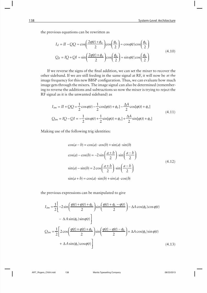
the previous equations can be rewritten as
ϕ φ φ φ ϕ
ϕ φ φ φ ϕ
+æ ö æ ö æ ö = - » »ç ÷ ç ÷ ç ÷ è ø è ø è ø
+æ ö æ ö æ ö = + » »ç ÷ ç ÷ ç ÷ è ø è ø è ø
2 ( )cos cos cos ( )cos
2 2 2
2 ( )sin cos sin ( )cos
2 2 2
e e ed
e e ed
t I II QQ t
t Q IQ QI t
(4.10)
If we reverse the signs of the final addition, we can set the mixer to recover theother sideband. If we are still feeding in the same signal at RF, it will now be at theimage frequency for this new BBSP configuration. Thus, we can evaluate how muchimage gets through the mixers. The image signal can also be determined (remember-ing to reverse the additions and subtractions so now the mixer is trying to reject theRF signal as it is the unwanted sideband) as
ϕ ϕ φ ϕ φ
ϕ ϕ φ ϕ φ
D= + = - + - +
D= - = - + + + +
1 1cos ( ) cos[ ( ) ] cos[ ( ) ]
2 2 2
1 1sin ( ) sin[ ( ) ] sin[ ( ) ]
2 2 2
im e e
im e e
AI II QQ t t t
AQ IQ QI t t t
(4.11)
Making use of the following trig identities:
cos( ) cos( ) cos( ) sin( ) sin( )
cos( ) cos( ) 2 sin sin2 2
sin( ) sin( ) 2 cos sin2 2
sin( ) cos( ) sin( ) sin( ) cos( )
a b a b a b
a b a ba b
a b a ba b
a b a b a b
- = × + ×
+ -æ ö æ ö - = - ×ç ÷ ç ÷ è ø è ø
+ -æ ö æ ö - = ×ç ÷ ç ÷ è ø è ø
+ = × + ×
(4.12)
the previous expressions can be manipulated to give
ϕ ϕ φ ϕ φ ϕ φ ϕ
φ ϕ
ϕ ϕ φ ϕ ϕ φ φ ϕ
φ ϕ
+ + + -æ ö æ ö = - - Dç ÷ ç ÷ ê è ø è ø ë
ù- D úû
é + + - -æ ö æ ö = + Dç ÷ ç ÷ ê è ø è ø ë
ù+ D ú
û
1 ( ) ( ) ( ) ( )2 sin sin cos( )cos ( )
2 2 2
sin( )sin ( )
1 ( ) ( ) ( ) ( )2 cos sin cos( )sin ( )
2 2 2
sin( )cos ( )
e eim e
e
e eim e
e
t t t t I A t
A t
t t t t Q A t
A t
(4.13)
ART_Rogers_Ch04.indd 138 Manila Typesetting Company 08/23/2013
8/11/2019 Rogers 537 CH04
http://slidepdf.com/reader/full/rogers-537-ch04 11/30
4.5 Low IF Transceiver 139
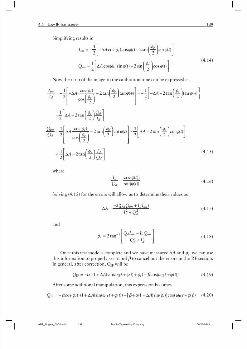
Simplifying results in
φ φ ϕ ϕ
φ φ ϕ ϕ
é ùæ ö » - -D - ç ÷ ê úè ø ë û
é ùæ ö » D - ç ÷ ê úè ø ë û
1cos( )cos ( ) 2 sin sin ( )
2 2
1cos( )sin ( ) 2 sin cos ( )
2 2
eim e
eim e
I A t t
Q A t t (4.14)
Now the ratio of the image to the calibration tone can be expressed as
1 cos( ) 1
2 tan tan ( ) 2 tan tan ( )2 2 2 2
cos2
1= 2 tan
2 2
1 cos( ) 12 tan cot ( ) 2 tan
2 2 2 2cos
2
im e e e
ed
e d
d
im e e e
ed
I A A
I
QA
I
QA t A
Q
φ φ φ ϕ ϕ
φ
φ
φ φ φ ϕ
φ
é ù é ùæ ö æ ö = - -D - + » - -D - +ç ÷ ç ÷ ê ú ê úè ø è ø æ ö ë ûê úç ÷ è ø ë û
é ùæ ö D + ç ÷ ê úè ø ë û
é ùæ ö æ ö = D - » D -ç ÷ çê úè ø è æ ö ê úç ÷ è ø ê úë û
cot ( )
12tan
2 2
e d
d
t
I A
Q
ϕ
φ
é ù÷ ê úø ë û
é ùæ ö = D - ç ÷ ê úè ø ë û
(4.15)
where
cos( ( ))sin( ( ))
d
d
I t Q t
ϕ
ϕ =
(4.16)
Solving (4.15) for the errors will allow us to determine their values as
2 2
2( )d im d im
d d
Q Q I I A
I Q
- +D =
+ (4.17)
and
1
2 22 tan
d im d im
ed d
Q I I Q
Q I φ
- é ù-
= ê ú+ê úë û (4.18)
Once this test mode is complete and we have measured DA and φ e, we can usethis information to properly set α and β to cancel out the errors in the RF section.In general, after correction, QIF will be
IF IF IF(1 )sin( ( ) ) cos( ( ))eQ A t t t t α ω ϕ φ β ω ϕ = - × + D + + + + (4.19)
After some additional manipulation, this expression becomes
α φ ω ϕ β α φ ω ϕ = - × + D + - + + D +
IF IF IFcos( ) (1 )sin( ( )) [ (1 )sin( )]cos( ( ))e eQ A t t A t t (4.20)
ART_Rogers_Ch04.indd 139 Manila Typesetting Company 08/23/2013
8/11/2019 Rogers 537 CH04
http://slidepdf.com/reader/full/rogers-537-ch04 12/30
140 System-Level Architecture
Ideally we would like
cos( ) (1 ) 1
(1 )sin( ) 0
e
e
A
A
α φ
β α φ
× + D =
+ + D =
(4.21)
Solving for α and β gives
1
(1 )cos( )
tan( )
e
e
Aα
φ
β φ
=+ D
= -
(4.22)
Example 4.1: Correcting for Amplitude and Phase Imbalance in a Low IF Receiver
A low IF receiver is to receive a 101-MHz RF signal and convert it to a 1-MHz IFusing a 100-MHz LO. There are errors in the RF part of the circuit. These need tobe corrected within the BBSP part of the radio. Simulate the system and determinethe correction coefficients needed.
Solution:
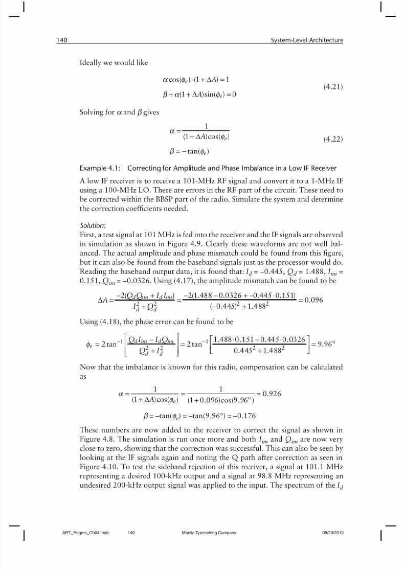
First, a test signal at 101 MHz is fed into the receiver and the IF signals are observedin simulation as shown in Figure 4.9. Clearly these waveforms are not well bal-anced. The actual amplitude and phase mismatch could be found from this figure,but it can also be found from the baseband signals just as the processor would do.Reading the baseband output data, it is found that: I d = −0.445, Qd = 1.488, I im =0.151, Qim = −0.0326. Using (4.17), the amplitude mismatch can be found to be
2 2 2 2
2( ) 2(1.488 0.0326 0.445 0.151)0.096
( 0.445) 1.488
d i m d im
d d
Q Q I I A
I Q
- + - - + - ×D = = =
+ - +
Using (4.18), the phase error can be found to be
1 1 o
2 2 2 2
1.488 0.151 0.445 0.03262 tan 2 tan 9.96
0.445 1.488
d im d ime
d d
Q I I Q
Q I φ - -
é ù- × - ×é ù= = =ê ú ê ú+ +ë ûê úë û
Now that the imbalance is known for this radio, compensation can be calculatedas
o
1 1 0.926(1 )cos( ) (1 0.096)cos(9.96 )eA
α φ
= = =+ D +
β = –tan(φ e) = –tan(9.96°) = –0.176
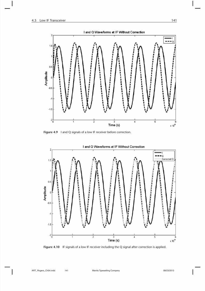
These numbers are now added to the receiver to correct the signal as shown inFigure 4.8. The simulation is run once more and both I im and Qim are now veryclose to zero, showing that the correction was successful. This can also be seen bylooking at the IF signals again and noting the Q path after correction as seen inFigure 4.10. To test the sideband rejection of this receiver, a signal at 101.1 MHzrepresenting a desired 100-kHz output and a signal at 98.8 MHz representing an
undesired 200-kHz output signal was applied to the input. The spectrum of the I d
ART_Rogers_Ch04.indd 140 Manila Typesetting Company 08/23/2013
8/11/2019 Rogers 537 CH04
http://slidepdf.com/reader/full/rogers-537-ch04 13/30
4.5 Low IF Transceiver 141
Figure 4.9 I and Q signals of a low IF receiver before correction.
Figure 4.10 IF signals of a low IF receiver including the Q signal after correction is applied.
ART_Rogers_Ch04.indd 141 Manila Typesetting Company 08/23/2013

8/11/2019 Rogers 537 CH04
http://slidepdf.com/reader/full/rogers-537-ch04 14/30
142 System-Level Architecture
output is shown in Figure 4.11. This figure shows nearly perfect image rejection.Note that the simulation of this receiver is ideal except for the modeled imperfec-
tions explicitly stated in the RF section.
4.6 Sliding IF Transceiver
An architecture that is a compromise between the superheterodyne and the direct-conversion transceiver is called a sliding IF architecture shown in Figure 4.12. This
Figure 4.11 Spectrum of the ID signal of a low IF receiver showing rejection of the unwantedsideband.
Mixer
upconverter
AGC
AGC
IQ Demod
90°÷M
Image
Filter
Power Amp
LNA
Preselect
BPF
Switch
BPF
Rx
Tx
Antenna
Driver
BBFilters
BBFilters
To DSP
From DSP
AGC
AGC
AGC
AGC
A/D
D/A
LO_I
LO_I
I_Rx
Q_Rx
I_Tx
Q_Tx
LO_Q
LO_Q
RFSynthesizer
Figure 4.12 A sliding IF radio architecture.
ART_Rogers_Ch04.indd 142 Manila Typesetting Company 08/23/2013
8/11/2019 Rogers 537 CH04
http://slidepdf.com/reader/full/rogers-537-ch04 15/30
4.7 An Upconversion-Downconversion Receiver Architecture 143
architecture derives the IF LO by dividing the RF LO by some fixed number. As aresult, the IF frequency is not fixed, but “walks” in step with a fraction of the fre-quency of the RF LO. This transceiver with sliding IF still has many of the advan-tages of the superheterodyne radio (although it is not possible to filter as well at IF),
but also removes the need for the extra synthesizer, potentially reducing layout areaand power dissipation. Additionally, as there is only one synthesizer, this avoids thepossibility of two synthesizer output frequencies mixing together to produce beatfrequencies possibly in the baseband.
4.7 An Upconversion-Downconversion Receiver Architecture
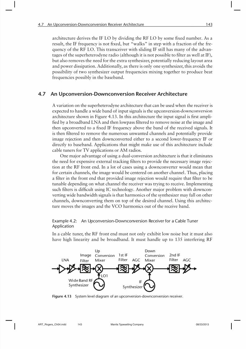
A variation on the superheterodyne architecture that can be used when the receiver isexpected to handle a wide band of input signals is the upconversion-downconversion
architecture shown in Figure 4.13. In this architecture the input signal is first ampli-fied by a broadband LNA and then lowpass filtered to remove noise at the image andthen upconverted to a fixed IF frequency above the band of the received signals. Itis then filtered to remove the numerous unwanted channels and potentially provideimage rejection and then downconverted either to a second lower-frequency IF ordirectly to baseband. Applications that might make use of this architecture includecable tuners for TV applications or AM radios.
One major advantage of using a dual-conversion architecture is that it eliminatesthe need for expensive external tracking filters to provide the necessary image rejec-tion at the RF front end. In a lot of cases using a downconverter would mean thatfor certain channels, the image would be centered on another channel. Thus, placing
a filter in the front end that provided image rejection would require that filter to betunable depending on what channel the receiver was trying to receive. Implementingsuch filters is difficult using IC technology. Another major problem with downcon-verting wide bandwidth signals is that harmonics of the synthesizer may fall on otherchannels, downconverting them on top of the desired channel. Using this architec-ture moves the images and the VCO harmonics out of the receive band.
Example 4.2: An Upconversion-Downconversion Receiver for a Cable Tuner Application
In a cable tuner, the RF front end must not only exhibit low noise but it must also
have high linearity and be broadband. It must handle up to 135 interfering RF
Image
Filter LNA AGC
1st IFFilter
Wide Band RFSynthesizer
IF
Synthesizer
LO1
AGC
2nd IFFilter
UpConversionMixer
DownConversionMixer
Figure 4.13 System level diagram of an upconversion-downconversion receiver.
ART_Rogers_Ch04.indd 143 Manila Typesetting Company 08/23/2013
8/11/2019 Rogers 537 CH04
http://slidepdf.com/reader/full/rogers-537-ch04 16/30
144 System-Level Architecture
channels at +15 dBmV over a frequency range from 47 to 870 MHz. Determine abasic receiver frequency plan to handle this situation.
Solution:
As this is a wideband input, an upconversion-downconversion architecture is chosen.The first IF frequency is chosen to be 1,890 MHz (the European DECT frequency) toeliminate in-band lower-order beat products between the first and second VCO on thechip and to keep the filter cost low due to its high-volume usage. To tune to this IFfrequency, a high-side LO is chosen for the wideband RF frequency synthesizer with arange from 1,936 to 2,760 MHz, which places the image frequency range from 3,826to 4,650 MHz. The front-end filter can easily reject this first image. The main purposeof the RF front end is to convert the incoming band of RF signals to a single IF fre-quency such that channel selectivity can be achieved by subsequent filtering. After thefirst IF filter only a few channels will remain and as will be seen in Chapter 5, this willgreatly reduce the linearity requirement of the second mixer block. The second LOfrequency can be a fixed number. Choosing a low-side injected LO sets the frequencyof this synthesizer at 1,840 MHz to provide a second IF frequency of 50 MHz.
4.8 Coherent Versus Noncoherent Receivers
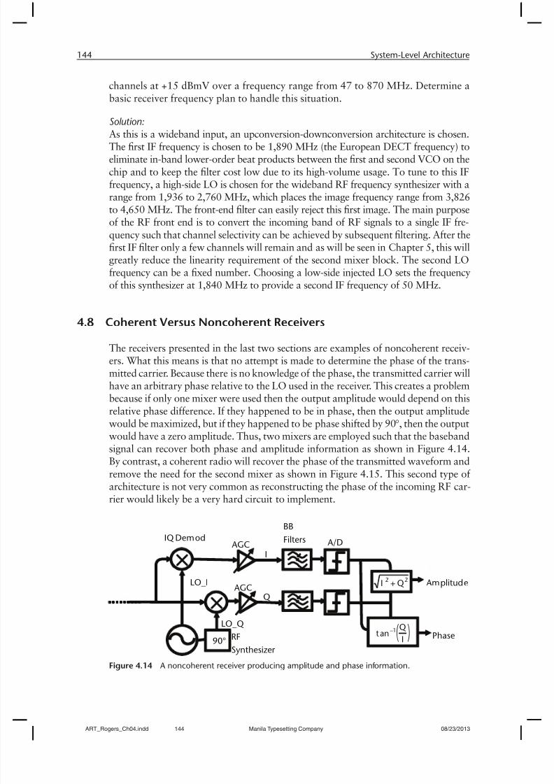
The receivers presented in the last two sections are examples of noncoherent receiv-ers. What this means is that no attempt is made to determine the phase of the trans-mitted carrier. Because there is no knowledge of the phase, the transmitted carrier willhave an arbitrary phase relative to the LO used in the receiver. This creates a problem
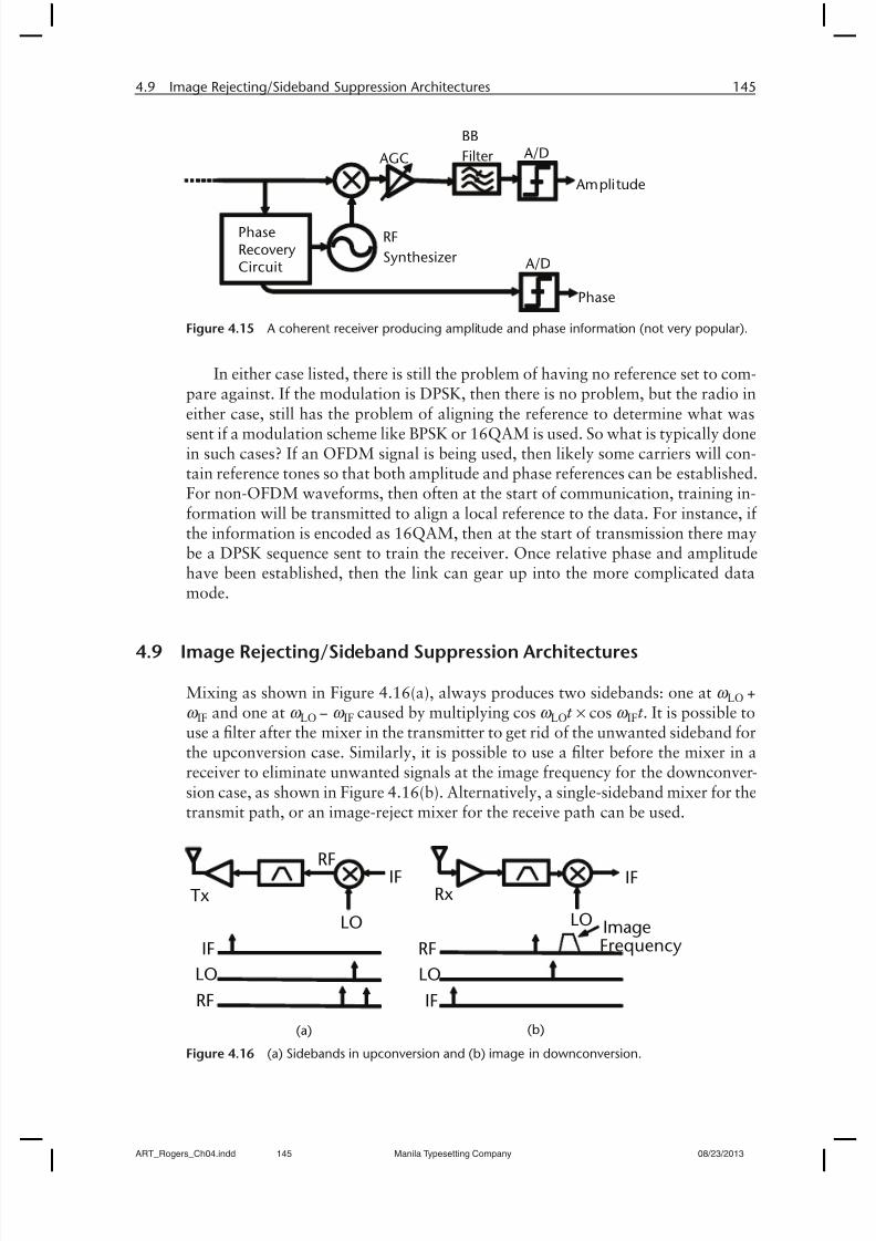
because if only one mixer were used then the output amplitude would depend on thisrelative phase difference. If they happened to be in phase, then the output amplitudewould be maximized, but if they happened to be phase shifted by 90°, then the outputwould have a zero amplitude. Thus, two mixers are employed such that the basebandsignal can recover both phase and amplitude information as shown in Figure 4.14.By contrast, a coherent radio will recover the phase of the transmitted waveform andremove the need for the second mixer as shown in Figure 4.15. This second type ofarchitecture is not very common as reconstructing the phase of the incoming RF car-rier would likely be a very hard circuit to implement.
IQ Demod
BB
Filters
RF
Synthesizer 90°
AGC
AGC A/D
LO_I
LO_Q
Amplitude
Phase
I
Q
22QI +
I
Qt an
–1( (
Figure 4.14 A noncoherent receiver producing amplitude and phase information.
ART_Rogers_Ch04.indd 144 Manila Typesetting Company 08/23/2013
8/11/2019 Rogers 537 CH04
http://slidepdf.com/reader/full/rogers-537-ch04 17/30
4.9 Image Rejecting/Sideband Suppression Architectures 145
In either case listed, there is still the problem of having no reference set to com-pare against. If the modulation is DPSK, then there is no problem, but the radio in
either case, still has the problem of aligning the reference to determine what wassent if a modulation scheme like BPSK or 16QAM is used. So what is typically donein such cases? If an OFDM signal is being used, then likely some carriers will con-tain reference tones so that both amplitude and phase references can be established.For non-OFDM waveforms, then often at the start of communication, training in-formation will be transmitted to align a local reference to the data. For instance, ifthe information is encoded as 16QAM, then at the start of transmission there maybe a DPSK sequence sent to train the receiver. Once relative phase and amplitudehave been established, then the link can gear up into the more complicated datamode.
4.9 Image Rejecting/Sideband Suppression Architectures
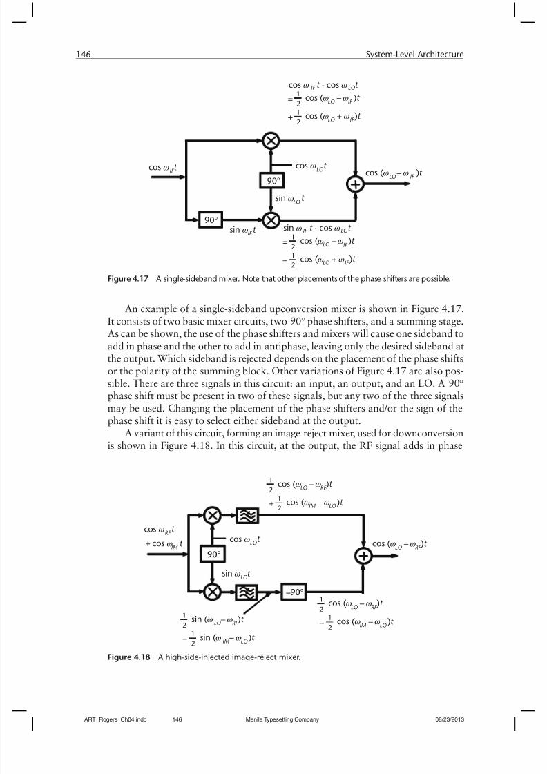
Mixing as shown in Figure 4.16(a), always produces two sidebands: one at ω LO +ω IF and one at ω LO − ω IF caused by multiplying cos ω LOt ´ cos ω IFt . It is possible touse a filter after the mixer in the transmitter to get rid of the unwanted sideband forthe upconversion case. Similarly, it is possible to use a filter before the mixer in areceiver to eliminate unwanted signals at the image frequency for the downconver-sion case, as shown in Figure 4.16(b). Alternatively, a single-sideband mixer for thetransmit path, or an image-reject mixer for the receive path can be used.
BB
Filter
RF
Synthesizer
AGC A/D
Amplitude
Phase
A/D
PhaseRecoveryCircuit
Figure 4.15 A coherent receiver producing amplitude and phase information (not very popular).
RFIF
Tx
LO
IF
LO
RF
RxIF
IF
LO
RFImageFrequency
(a) (b)
LO
Figure 4.16 (a) Sidebands in upconversion and (b) image in downconversion.
ART_Rogers_Ch04.indd 145 Manila Typesetting Company 08/23/2013
8/11/2019 Rogers 537 CH04
http://slidepdf.com/reader/full/rogers-537-ch04 18/30
146 System-Level Architecture
An example of a single-sideband upconversion mixer is shown in Figure 4.17.It consists of two basic mixer circuits, two 90° phase shifters, and a summing stage.As can be shown, the use of the phase shifters and mixers will cause one sideband toadd in phase and the other to add in antiphase, leaving only the desired sideband atthe output. Which sideband is rejected depends on the placement of the phase shiftsor the polarity of the summing block. Other variations of Figure 4.17 are also pos-sible. There are three signals in this circuit: an input, an output, and an LO. A 90°
phase shift must be present in two of these signals, but any two of the three signalsmay be used. Changing the placement of the phase shifters and/or the sign of thephase shift it is easy to select either sideband at the output.
A variant of this circuit, forming an image-reject mixer, used for downconversionis shown in Figure 4.18. In this circuit, at the output, the RF signal adds in phase
LO
IF
IF
cos ω t · cos ω t IF
cos ( ω – ω )t 1
2 LO=
cos ( ω + ω )t 1
2 LO+
cos ω t IF
sin ω t LO
cos ω t LO
sin ω t IF
sin ω t · cos ω t IF
cos ( ω – ω )t 1
2 LO=
cos ( ω
+ ω
)t
1
2 LO–
LO
IF
IF
LOcos ( ω – ω )t
IF
90°
90°
Figure 4.17 A single-sideband mixer. Note that other placements of the phase shifters are possible.
RF
LO
cos ( ω – ω )t 1
2 LO
cos ( ω – ω )t 1
2 IM +
RF
LO
cos ( ω – ω )t 1
2 LO
cos ( ω – ω )t 1
2 IM –RF
LO
sin ( ω – ω )t 1
2 LO
sin ( ω – ω )t 1
2 IM –
cos ω t RF
cos ω t IM
+cos ω t
LO
sin ω t LO
90°
–90°
RF cos ( ω – ω )t
LO
Figure 4.18 A high-side-injected image-reject mixer.
ART_Rogers_Ch04.indd 146 Manila Typesetting Company 08/23/2013
8/11/2019 Rogers 537 CH04
http://slidepdf.com/reader/full/rogers-537-ch04 19/30
4.10 An Alternative Single-Sideband Mixer 147
while the image adds in antiphase. Note that two LPFs are added after the mixers toremove the high-frequency summing terms at ω ω +LO RF and ω ω +LO IM.
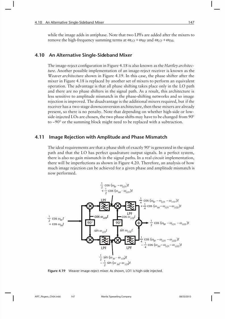
4.10 An Alternative Single-Sideband Mixer
The image-reject configuration in Figure 4.18 is also known as the Hartley architec-ture. Another possible implementation of an image-reject receiver is known as theWeaver architecture shown in Figure 4.19. In this case, the phase shifter after themixer in Figure 4.18 is replaced by another set of mixers to perform an equivalentoperation. The advantage is that all phase shifting takes place only in the LO pathand there are no phase shifters in the signal path. As a result, this architecture isless sensitive to amplitude mismatch in the phase-shifting networks and so imagerejection is improved. The disadvantage is the additional mixers required, but if the
receiver has a two-stage downconversion architecture, then these mixers are alreadypresent, so there is no penalty. Note that depending on whether high-side or low-side-injected LOs are chosen, the two phase shifts may have to be changed from 90° to −90° or the summing block might need to be replaced with a subtraction.
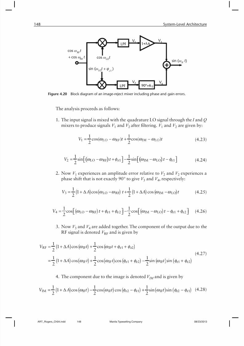
4.11 Image Rejection with Amplitude and Phase Mismatch
The ideal requirements are that a phase shift of exactly 90° is generated in the signalpath and that the LO has perfect quadrature output signals. In a perfect system,there is also no gain mismatch in the signal paths. In a real circuit implementation,
there will be imperfections as shown in Figure 4.20. Therefore, an analysis of howmuch image rejection can be achieved for a given phase and amplitude mismatch isnow performed.
90°
LPF
LPF LPF
LPF
cos ω t 12 RF
+ cos ω t IM
cos ( ω – ω )t 1
2 RF LO1
+IM
1
2cos ( ω – ω )t
LO1
cos ( ω – ω – ω )t 1
4 RF LO1 LO2
+IM
1
4cos ( ω – ω – ω )t
LO1 LO2
cos ( ω – ω – ω )t 1
2 RF LO1 LO2
cos ( ω – ω – ω )t 1
4 RF LO1 LO2
– IM
1
4cos ( ω – ω – ω )t
LO1 LO2
sin ( ω – ω )t 1
2 RF LO1
– IM
1
2sin ( ω – ω )t
LO1
cos ω t LO1cos ω t LO1 cos ω t LO2
sin ω t LO1
sin ω t LO2
90°
Figure 4.19 Weaver image-reject mixer. As shown, LO1 is high-side injected.
ART_Rogers_Ch04.indd 147 Manila Typesetting Company 08/23/2013
8/11/2019 Rogers 537 CH04
http://slidepdf.com/reader/full/rogers-537-ch04 20/30
148 System-Level Architecture
The analysis proceeds as follows:
The input signal is mixed with the quadrature LO signal through the1. I and Q mixers to produce signals V 1 and V 2 after filtering. V 1 and V 2 are given by:
11 1
cos( ) cos( )2 2
LO RF IM LOV t t ω ω ω ω = - + - (4.23)
( ) ( )2 LO RF 1 IM LO 1
1 1sin sin
2 2V t t ε ε ω ω φ ω ω φ é ù é ù= - + - - -ë û ë û (4.24)
Now2. V 1 experiences an amplitude error relative to V 2 and V 2 experiences aphase shift that is not exactly 90° to give V 3 and V 4, respectively:
( ) ( ) ( ) ( )ω ω ω ω = + D - + + D -3 LO RF IM LO
1 11 cos 1 cos
2 2V A t A t (4.25)
( ) ( )ε ε ε ε ω ω φ φ ω ω φ φ é ù é ù= - + + - - - +ë û ë û4 LO RF 1 2 IM LO 1 2
1 1cos cos
2 2V t t (4.26)
Now3. V 3 and V 4 are added together. The component of the output due to theRF signal is denoted V RF and is given by
( ) ( ) ( )
( ) ( ) ( ) ( ) ( ) ( )
ε ε
ε ε ε ε
ω ω φ φ
ω ω φ φ ω φ φ
= + D + + +
= + D + + - +
RF IF IF 1 2
IF IF 1 2 IF 1 2
1 11 cos cos
2 2
1 1 11 cos cos cos sin sin
2 2 2
V A t t
A t t t
(4.27)
The component due to the image is denoted4. V IM and is given by
( ) ( ) ( ) ( ) ( ) ( )ε ε ε ε ω ω φ φ ω φ φ = + D - - + -IM IF IF 2 1 IF 2 1
1 1 11 cos cos cos sin sin
2 2 2
V A t t t (4.28)
LPF 90º+ 2
V 1
V 2
V 3
V 4
1+ A LPF
cos ω t RF
cos ωt
IM + cos ωt
LO sin ( ω t )IF
sin ( ω t + φ )LO ε1
Figure 4.20 Block diagram of an image-reject mixer including phase and gain errors.
ART_Rogers_Ch04.indd 148 Manila Typesetting Company 08/23/2013
8/11/2019 Rogers 537 CH04
http://slidepdf.com/reader/full/rogers-537-ch04 21/30
4.12 LO Generation 149
Only the ratio of the magnitudes is important. The magnitudes are given5.by
( ) ( ) ( )
( ) ( ) ( )
ε ε ε ε
ε ε
φ φ φ φ
φ φ
é ùé ù é ù= + + + D + +ë û ë ûê úë û
é ù= + + D + + D +ë û
2 22
1 2 1 2
2
1 2
1sin 1 cos
4
11 1 2 1 cos
4
RFV A
A A
(4.29)
( )( ) ( ) ( )
( ) ( ) ( )
ε ε ε ε
ε ε
φ φ φ φ
φ φ
é ùé ù= - + + D - -ë ûê úë û
é ù= + + D - + D -ë û
2 22
2 1 2 1
2
2 1
1sin 1 cos
4
11 1 2 1 cos
4
IMV A
A A
(4.30)
Therefore, the image rejection ratio is given by6.
2 2RF 1 2
2 22 1IM
1 (1 ) 2(1 )cos( )IRR 10log 10log
1 (1 ) 2(1 )cos( )
V A A
A AV
ε ε
ε ε
φ φ
φ φ
ì ü+ + D + + D +ï ï= = í ý
+ + D - + D -ï ïî þ (4.31)
If there is no phase imbalance and no amplitude mismatch, then this equationapproaches infinity, and so ideally this system will reject the image perfectly. It isonly the nonideality of the components that cause finite image rejection. Figure4.21 shows a contour plot of how much image rejection can be expected for vari-ous levels of phase and amplitude mismatch. An amplitude error of about 20% isacceptable for 20 dB of image rejection, but more like 2% is required for 40 dB of
image rejection. Likewise, a phase mismatch must be held to less than 1.2° for 40dB of image rejection, while a phase mismatch of less than 11.4° can be toleratedfor 20 dB of image rejection.
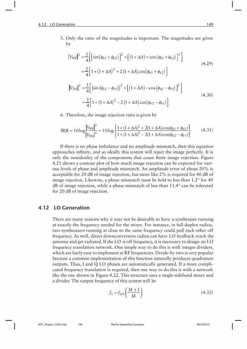
4.12 LO Generation
There are many reasons why it may not be desirable to have a synthesizer runningat exactly the frequency needed for the mixer. For instance, in full-duplex radios,two synthesizers running at close to the same frequency could pull each other off
frequency. As well, direct downconversion radios can have LO feedback reach theantenna and get radiated. If the LO is off frequency, it is necessary to design an LOfrequency translation network. One simple way to do this is with integer dividers,which are fairly easy to implement at RF frequencies. Divide-by-two is very popularbecause a common implementation of this function naturally produces quadratureoutputs. Thus, I and Q LO phases are automatically generated. If a more compli-cated frequency translation is required, then one way to do this is with a networklike the one shown in Figure 4.22. This structure uses a single-sideband mixer anda divider. The output frequency of this system will be
±æ ö = ç ÷
è ø
1o syn
Mf f
M
(4.32)
ART_Rogers_Ch04.indd 149 Manila Typesetting Company 08/23/2013

8/11/2019 Rogers 537 CH04
http://slidepdf.com/reader/full/rogers-537-ch04 22/30
150 System-Level Architecture
The choice of the plus or minus in the previous equation depends on which side-band the single-sideband mixer selects.
Example 4.3 Generating a Reference Tone
A GPS receiver that operates at 1.575 GHz is to be integrated with a 2.4-GHzWLAN chip. How can the synthesizer be reused for the GPS receiver?
= 2.29°
= 3.44°
= 4.58°
= 5.73°
= 1.15°
= 0°
I m a g e R e j e c t i o n
( d B )
45
40
35
30
25
20
Amplitude Error (%)-10 -8 -6 -4 -2 0 2 4 6 8 10
I m a g e R e j e c t i o n ( d B )45
40
35
30
25
20
Phase Error (degrees)-6 -4 -2 0 2 4 6
50 A = 0%
A = 2%
A = 4%
A = 6%
A = 8%
A = 10%
Figure 4.21 Plot of image rejection versus phase and amplitude mismatch.
÷M
Synthesizer SSB Mixer f syn
f syn/M
f o
Figure 4.22 Frequency generation network using a single-sideband mixer.
ART_Rogers_Ch04.indd 150 Manila Typesetting Company 08/23/2013
8/11/2019 Rogers 537 CH04
http://slidepdf.com/reader/full/rogers-537-ch04 23/30
4.12 LO Generation 151
Solution:
If the WLAN synthesizer can be tuned above the band to 2.625 GHz, then usinga division ratio of 3/5 will yield the GPS frequency. If we use the divider structureshown in Figure 4.22 with M = 5, using the higher-frequency output yields a 6/5
output. Following the output with a divide by two will give an overall output at 3/5of the input frequency.
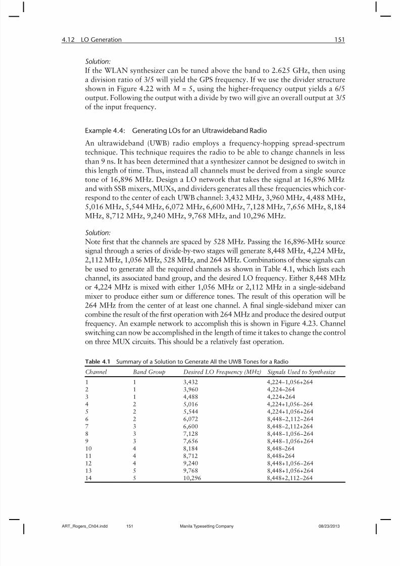
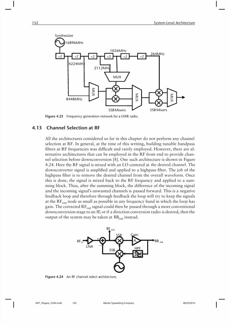
Example 4.4: Generating LOs for an Ultrawideband Radio
An ultrawideband (UWB) radio employs a frequency-hopping spread-spectrumtechnique. This technique requires the radio to be able to change channels in lessthan 9 ns. It has been determined that a synthesizer cannot be designed to switch inthis length of time. Thus, instead all channels must be derived from a single sourcetone of 16,896 MHz. Design a LO network that takes the signal at 16,896 MHz
and with SSB mixers, MUXs, and dividers generates all these frequencies which cor-respond to the center of each UWB channel: 3,432 MHz, 3,960 MHz, 4,488 MHz,5,016 MHz, 5,544 MHz, 6,072 MHz, 6,600 MHz, 7,128 MHz, 7,656 MHz, 8,184MHz, 8,712 MHz, 9,240 MHz, 9,768 MHz, and 10,296 MHz.
Solution:
Note first that the channels are spaced by 528 MHz. Passing the 16,896-MHz sourcesignal through a series of divide-by-two stages will generate 8,448 MHz, 4,224 MHz,2,112 MHz, 1,056 MHz, 528 MHz, and 264 MHz. Combinations of these signals canbe used to generate all the required channels as shown in Table 4.1, which lists eachchannel, its associated band group, and the desired LO frequency. Either 8,448 MHz
or 4,224 MHz is mixed with either 1,056 MHz or 2,112 MHz in a single-sidebandmixer to produce either sum or difference tones. The result of this operation will be264 MHz from the center of at least one channel. A final single-sideband mixer cancombine the result of the first operation with 264 MHz and produce the desired outputfrequency. An example network to accomplish this is shown in Figure 4.23. Channelswitching can now be accomplished in the length of time it takes to change the controlon three MUX circuits. This should be a relatively fast operation.
Table 4.1 Summary of a Solution to Generate All the UWB Tones for a Radio
Channel Band Group Desired LO Frequency (MHz) Signals Used to Synthesize
1 1 3,432 4,224−1,056+2642 1 3,960 4,224–264
3 1 4,488 4,224+2644 2 5,016 4,224+1,056−2645 2 5,544 4,224+1,056+264
6 2 6,072 8,448−2,112−2647 3 6,600 8,448−2,112+2648 3 7,128 8,448−1,056−264
9 3 7,656 8,448−1,056+26410 4 8,184 8,448–26411 4 8,712 8,448+264
12 4 9,240 8,448+1,056−26413 5 9,768 8,448+1,056+26414 5 10,296 8,448+2,112−264
ART_Rogers_Ch04.indd 151 Manila Typesetting Company 08/23/2013
8/11/2019 Rogers 537 CH04
http://slidepdf.com/reader/full/rogers-537-ch04 24/30
152 System-Level Architecture
4.13 Channel Selection at RF
All the architectures considered so far in this chapter do not perform any channelselection at RF. In general, at the time of this writing, building tunable bandpassfilters at RF frequencies was difficult and rarely employed. However, there are al-ternative architectures that can be employed in the RF front end to provide chan-nel selection before downconversion [8]. One such architecture is shown in Figure
4.24. Here the RF signal is mixed with an LO centered at the desired channel. Thedownconverter signal is amplified and applied to a highpass filter. The job of thehighpass filter is to remove the desired channel from the overall waveform. Oncethis is done, the signal is mixed back to the RF frequency and applied to a sum-ming block. Thus, after the summing block, the difference of the incoming signaland the incoming signal’s unwanted channels is passed forward. This is a negativefeedback loop and therefore through feedback the loop will try to keep the signalsat the RFout node as small as possible in any frequency band in which the loop hasgain. The corrected RFout signal could then be passed through a more conventionaldownconversion stage to an IF, or if a direction conversion radio is desired, then theoutput of the system may be taken at BBout instead.
Synthesizer
16896MHz
÷2 ÷2 ÷2
8448MHz
4224MHz
÷2
2112MHz
÷2
1056MHz
÷2 264MHz
MUX
M U X M
U X
M U X
SSB Mixers SSB MixersFigure 4.23 Frequency generation network for a UWB radio.
Gain
LNA
RF in+
–
HPF
RF out
BB out A v
SSB
SSB
Figure 4.24 An RF channel select architecture.
ART_Rogers_Ch04.indd 152 Manila Typesetting Company 08/23/2013
8/11/2019 Rogers 537 CH04
http://slidepdf.com/reader/full/rogers-537-ch04 25/30
4.14 Transmitter Linearity Techniques 153
Assuming that the mixers in Figure 4.24 are ideal, the transfer function of sys-tem can be determined. For simplicity, assuming that the gain of the LNA is unity,the transfer function of the system is given by
( )1 ( )
out v
in v
BB AT sRF A H s
= =
+
(4.33)
where H (s) is the transfer function of the highpass filter. If the highpass filter isassumed to be a simple first-order structure such that
( )o
sH s
s ω
=
+
(4.34)
then (4.33) can be expanded to give
( )1
( )
1
v o
v
o
v
As
AT s
sA
ω
ω
æ ö +ç ÷ è ø +=
++
(4.35)
This transfer function contains one zero and one pole. Knowing the bandwidth ofthe desired signal, ω o should be chosen to be
(1 )o vBW Aω = + (4.36)
Note that at RF the shape of the frequency response would be the same except it
would be centered at the LO frequency rather than at DC.
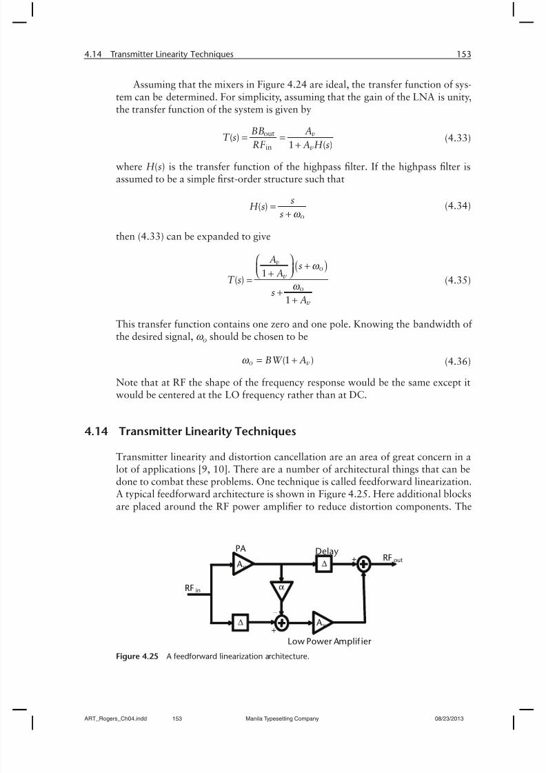
4.14 Transmitter Linearity Techniques
Transmitter linearity and distortion cancellation are an area of great concern in alot of applications [9, 10]. There are a number of architectural things that can bedone to combat these problems. One technique is called feedforward linearization.A typical feedforward architecture is shown in Figure 4.25. Here additional blocksare placed around the RF power amplifier to reduce distortion components. The
PA
RF in
+
–
RF out Av
Low Power Amplif ier
Av
+
–
Delay
Figure 4.25 A feedforward linearization architecture.
ART_Rogers_Ch04.indd 153 Manila Typesetting Company 08/23/2013
8/11/2019 Rogers 537 CH04
http://slidepdf.com/reader/full/rogers-537-ch04 26/30
154 System-Level Architecture
output of the main power amplifier is sensed by an attenuator with a loss of α . Notethat α is normally set to be equal to 1/ Av. The output of this attenuator is subtractedfrom a delayed version of the input. The delay is included to make sure that thephases are aligned. The idea is that the output of the lower summing block now in-
cludes only the distortion components with the main (desired) signal removed. Theresult is passed through a low-power amplifier and then subtracted from the mainoutput. The gain of the low-power amplifier should match the main power ampli-fier gain. After the addition, the resulting output RFout should contain the desiredsignal with no distortion.
While the feedforward technique can work very well, it depends on the gains ofthe amplifiers to be matched, the low-power amplifier to be linear, and the delays tomatch the delays through the corresponding amplifiers. If any of these parametersare wrong or incorrectly tuned, the amount of distortion cancellations will decreaseproportionally.
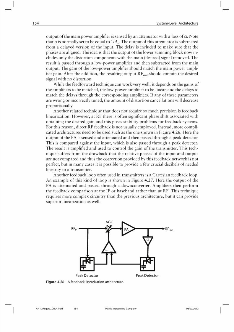
Another related technique that does not require so much precision is feedbacklinearization. However, at RF there is often significant phase shift associated withobtaining the desired gain and this poses stability problems for feedback systems.For this reason, direct RF feedback is not usually employed. Instead, more compli-cated architectures need to be used such as the one shown in Figure 4.26. Here theoutput of the PA is sensed and attenuated and then passed through a peak detector.This is compared against the input, which is also passed through a peak detector.The result is amplified and used to control the gain of the transmitter. This tech-nique suffers from the drawback that the relative phases of the input and outputare not compared and thus the correction provided by this feedback network is notperfect, but in many cases it is possible to provide a few crucial decibels of needed
linearity to a transmitter.Another feedback loop often used in transmitters is a Cartesian feedback loop.
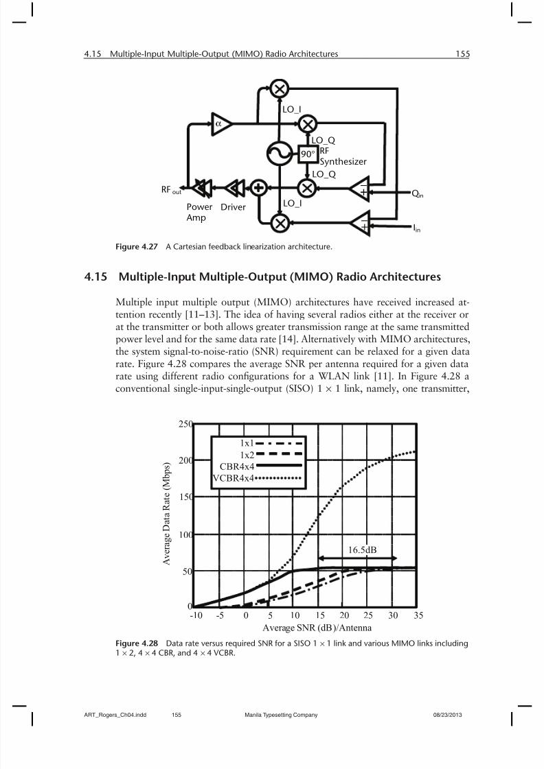
An example of this kind of loop is shown in Figure 4.27. Here the output of thePA is attenuated and passed through a downconverter. Amplifiers then performthe feedback comparison at the IF or baseband rather than at RF. This techniquerequires more complex circuitry than the previous architecture, but it can providesuperior linearization as well.
PA
Peak Detector
AGC
Peak Detector
RFin RF out
Figure 4.26 A feedback linearization architecture.
ART_Rogers_Ch04.indd 154 Manila Typesetting Company 08/23/2013
8/11/2019 Rogers 537 CH04
http://slidepdf.com/reader/full/rogers-537-ch04 27/30
4.15 Multiple-Input Multiple-Output (MIMO) Radio Architectures 155
4.15 Multiple-Input Multiple-Output (MIMO) Radio Architectures
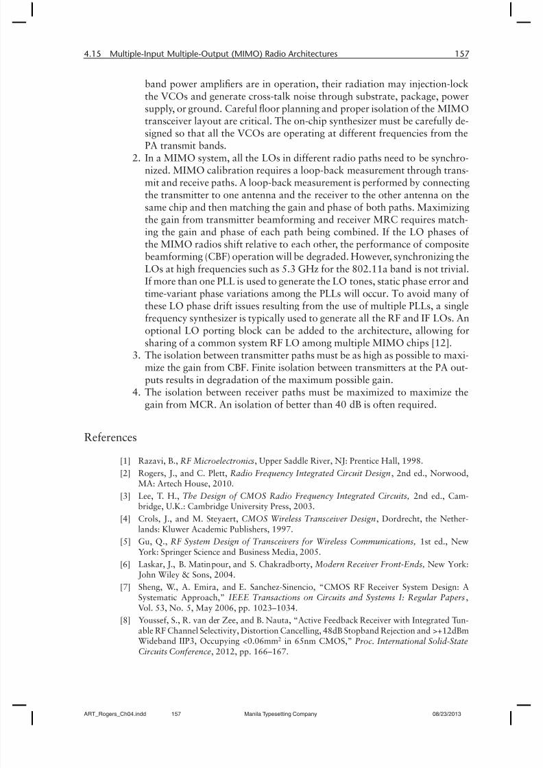
Multiple input multiple output (MIMO) architectures have received increased at-tention recently [11–13]. The idea of having several radios either at the receiver orat the transmitter or both allows greater transmission range at the same transmittedpower level and for the same data rate [14]. Alternatively with MIMO architectures,the system signal-to-noise-ratio (SNR) requirement can be relaxed for a given datarate. Figure 4.28 compares the average SNR per antenna required for a given datarate using different radio configurations for a WLAN link [11]. In Figure 4.28 a
conventional single-input-single-output (SISO) 1´ 1 link, namely, one transmitter,
RFSynthesizer
90°
Power Amp
Driver LO_I
LO_I
LO_Q
LO_Q
+
–++RF out
Iin
Qin
–
Figure 4.27 A Cartesian feedback linearization architecture.
250
200
150
100
50
0-10 10 30-5 0 20 25
Average SNR (dB)/Antenna
A v e r a g e D a
t a R a t e ( M b p s )
5 15 35
1x1
1x2
CBR4x4
VCBR4x4
16.5dB
Figure 4.28 Data rate versus required SNR for a SISO 1 ´ 1 link and various MIMO links including
1 ´ 2, 4 ´ 4 CBR, and 4 ´ 4 VCBR.
ART_Rogers_Ch04.indd 155 Manila Typesetting Company 08/23/2013

8/11/2019 Rogers 537 CH04
http://slidepdf.com/reader/full/rogers-537-ch04 28/30
156 System-Level Architecture
one receiver architecture is compared to various MIMO systems such as a 1 ´ 2 selec-tion diversity link (spatially separated receiver or transmitter antennas to select thestrongest signal), a 4 ´ 4 link that uses composite beamforming (CBF) technology andmaximal ratio combining, and a vector CBF (VCBF) link. From Figure 4.28 it can be
seen that at a data rate of 54 Mbps, the SNR required for a 4 ´ 4 link is 16.5 dB lowerthan that required by a 1 ´ 1 link, clearly demonstrating the advantages of MIMOarchitectures.
When using multiple radios, there is a trade-off between the level of integrationand the complexity and yield of the radio ICs. Integrating more radios togetherleads to more expensive packaging and lower yield, but lower cost and smalleroverall designs. However, for example, if a two-radio chip is used and if more thantwo radios are desired in a particular application, then even two, three, or moredual-radio transceiver chips can be used in a single link, provided that their localoscillators (LO) are all phase synchronized [12]. For instance, two pairs of dual-
radio transceiver chips can be used to form a 4´ 4 MIMO radio system as shownin Figure 4.29. Each transceiver pair consists of a master and a slave dual-radio
transceiver chip. The slave chip synchronizes its LO to the master chip by means ofthe LO porting circuitry, in which the master chip’s synthesizer can be used to drivethe slave chip’s LOs for synchronization.
MIMO transceiver design is a challenge due to the following issues:
When multiple radios are integrated in the same die, interference among the1.transceiver building blocks will be a big concern. In particular, when multi-
LO Porting Trace
Master Chip
Slave Chip
LO Porting Trace
Transmitting Radio
Master Chip
Slave Chip
Link
Receiving Radio
Beam Formingin the TX to get
antenna gain
through signal shaping
Maximum ratio
Combining at receive
of signals in four
paths at the RX
Note: Both beam
forming and maximum
ratio combining
controlled by DSP
Figure 4.29 A 4 ´ 4 MIMO system using two ICs each containing two radios.
ART_Rogers_Ch04.indd 156 Manila Typesetting Company 08/23/2013
8/11/2019 Rogers 537 CH04
http://slidepdf.com/reader/full/rogers-537-ch04 29/30
4.15 Multiple-Input Multiple-Output (MIMO) Radio Architectures 157
band power amplifiers are in operation, their radiation may injection-lockthe VCOs and generate cross-talk noise through substrate, package, powersupply, or ground. Careful floor planning and proper isolation of the MIMOtransceiver layout are critical. The on-chip synthesizer must be carefully de-
signed so that all the VCOs are operating at different frequencies from thePA transmit bands.In a MIMO system, all the LOs in different radio paths need to be synchro-2.nized. MIMO calibration requires a loop-back measurement through trans-mit and receive paths. A loop-back measurement is performed by connectingthe transmitter to one antenna and the receiver to the other antenna on thesame chip and then matching the gain and phase of both paths. Maximizingthe gain from transmitter beamforming and receiver MRC requires match-ing the gain and phase of each path being combined. If the LO phases ofthe MIMO radios shift relative to each other, the performance of composite
beamforming (CBF) operation will be degraded. However, synchronizing theLOs at high frequencies such as 5.3 GHz for the 802.11a band is not trivial.If more than one PLL is used to generate the LO tones, static phase error andtime-variant phase variations among the PLLs will occur. To avoid many ofthese LO phase drift issues resulting from the use of multiple PLLs, a singlefrequency synthesizer is typically used to generate all the RF and IF LOs. Anoptional LO porting block can be added to the architecture, allowing forsharing of a common system RF LO among multiple MIMO chips [12].The isolation between transmitter paths must be as high as possible to maxi-3.mize the gain from CBF. Finite isolation between transmitters at the PA out-puts results in degradation of the maximum possible gain.
The isolation between receiver paths must be maximized to maximize the4.gain from MCR. An isolation of better than 40 dB is often required.
References
[1] Razavi, B., RF Microelectronics, Upper Saddle River, NJ: Prentice Hall, 1998.
[2] Rogers, J., and C. Plett, Radio Frequency Integrated Circuit Design, 2nd ed., Norwood,MA: Artech House, 2010.
[3] Lee, T. H., The Design of CMOS Radio Frequency Integrated Circuits, 2nd ed., Cam-bridge, U.K.: Cambridge University Press, 2003.
[4] Crols, J., and M. Steyaert, CMOS Wireless Transceiver Design, Dordrecht, the Nether-lands: Kluwer Academic Publishers, 1997.
[5] Gu, Q., RF System Design of Transceivers for Wireless Communications, 1st ed., NewYork: Springer Science and Business Media, 2005.
[6] Laskar, J., B. Matinpour, and S. Chakradborty, Modern Receiver Front-Ends, New York: John Wiley & Sons, 2004.
[7] Sheng, W., A. Emira, and E. Sanchez-Sinencio, “CMOS RF Receiver System Design: ASystematic Approach,” IEEE Transactions on Circuits and Systems I: Regular Papers,Vol. 53, No. 5, May 2006, pp. 1023–1034.
[8] Youssef, S., R. van der Zee, and B. Nauta, “Active Feedback Receiver with Integrated Tun-able RF Channel Selectivity, Distortion Cancelling, 48dB Stopband Rejection and >+12dBmWideband IIP3, Occupying <0.06mm2 in 65nm CMOS,” Proc. International Solid-State
Circuits Conference, 2012, pp. 166–167.
ART_Rogers_Ch04.indd 157 Manila Typesetting Company 08/23/2013
8/11/2019 Rogers 537 CH04
http://slidepdf.com/reader/full/rogers-537-ch04 30/30