Embed Size (px)
Citation preview
Page 1 of 14
ELECTRICAL & ELECTRONIC ENGINEERING | SHORT COMMUNICATION
RF MEMS and CSRRs-based tunable filter designed for Ku and K bands applicationNgasepam Monica Devi, Santanu Maity, Rajesh Saha and Sanjeev Kumar Metya
Cogent Engineering (2015), 2: 1083641
Monica Devi et al., Cogent Engineering (2015), 2: 1083641http://dx.doi.org/10.1080/23311916.2015.1083641
ELECTRICAL & ELECTRONIC ENGINEERING | SHORT COMMUNICATION
RF MEMS and CSRRs-based tunable filter designed for Ku and K bands applicationNgasepam Monica Devi1, Santanu Maity2*, Rajesh Saha1 and Sanjeev Kumar Metya2
Abstract: This paper presents the design and simulation of a reconfigurable stop-band filter on a silicon substrate based on the combination of RF microelectrome-chanical system and metamaterial-based technologies. The device is implemented on coplanar waveguide structure by embedding complementary split-ring resona-tors on the central line and an RF MEMS varactor bridge supporting the neighboring ground planes. The response characteristics of this metamaterial-based filter can be dynamically tuned, thus enhancing its usefulness. The device operates within a frequency range of 16.5–19.5 GHz, giving a tuning range of 15%, and can be tuned from Ku-frequency band to K-frequency band. It works with a comparative low pull-in voltage of 17.42 V and a faster switching time of 0.138 µs. A thorough elec-tromechanical analysis has been done by varying various structural and material parameters. Moreover, a comparative electrical performance of silicon and glass has been shown to overcome the cons of silicon by high-resistivity glass.
Subjects: Circuits & Devices; Electrical & Electronic Engineering; Electromagnetics & Communication
Keywords: complementary split-ring resonators; coplanar waveguide; metamaterials; microelectromechanical system; tunable filters
*Corresponding author: Santanu Maity, Electronics and Communication Engineering, National Institute of Technology, Arunachal Pradesh, Yupia 791112, India E-mail: [email protected]
Reviewing editor:Qingsong Ai, Wuhan University of Technology, China
Additional information is available at the end of the article
ABOUT THE AUTHORSantanu Maity is working as assistant professor in the Department of Electronics and Communication Engineering at National Institute of Technology, Arunachal Pradesh, India. His research interest in RF MEMS based switch, MEMS based gas sensor, Crystalline Si solar cell, Semiconductor devices etc. He has more than four years of research experience on nano fabrication facility at Jadavpur University, IITB & IIEST.
PUBLIC INTEREST STATEMENTMicroelectromechanical system (MEMS) are types of miniature devices as well as systems fabricated on different platforms by micromachining processes. The work showed numerous parametric analyses of various parameters related to the RF MEMS varactor bridge used. Also, this work has addressed RF MEMS switch problem by achieving a lower actuation voltage of 17.42 V and a comparatively faster switching time of 0.138 µs. Also, through the material property analyses of various MEMS beams, the problem of selection of the material with respect to the requirements such as need for low pull-in voltage and high spring constant has also been solved. The tunability of the complementary split-ring resonator filter has been achieved through the implementation of MEMS varactor bridges only. In fact, this work has given a vivid idea on how MEMS technology can give good tunability through optimized device dimensions.
Received: 28 May 2015Accepted: 11 August 2015Published: 14 September 2015
© 2015 The Author(s). This open access article is distributed under a Creative Commons Attribution (CC-BY) 4.0 license.
Page 2 of 14
Santanu Maity
Page 3 of 14
Monica Devi et al., Cogent Engineering (2015), 2: 1083641http://dx.doi.org/10.1080/23311916.2015.1083641
1. IntroductionMicroelectromechanical system (MEMS) is a collection of sensors and actuators that have the ability to sense its environment and function according to the various changes in that environment with the use of a microcircuit control. Thus, MEMS has microelectronics packaging, antenna structures, micropower supply, microrelay, and microsignal processing units (Jason Yao, 2000). The popularity of MEMS is increasing day by day. Thus, numerous MEMS structures have been proposed and designed in various fields, such as microfluidics, aerospace, biomedical, chemical analysis, wireless communications, data storage, display, optics, etc. Still the feasibility of designing more complex MEMS structures is in progress.
Nowadays, many structures based on MEMS are used in RF domain. There are various types of RF micro-electromechanical system (RF MEMS) components, which can be in the form of switches, switched capaci-tors, tunable inductors, resonators, filters and varactors. These devices can be used instead of FETs, HEMTs and PIN diodes due to the advantages these offer, such as reduction in cost due to batch fabrication; down-scaling in dimensions, which leads to advancements in performance; reduction in size and weight to a large extent; and its integrating capability with microwave-integrated circuit through passive fabrica-tion techniques (Jason Yao, 2000; Vu, Prigent, Ruan, & Plana, 2012). MEMS devices are fabricated using silicon micromachining technique. In silicon micromachining, the structures are made 3-dimensional by either etching silicon substrate or by forming micromechanical layers from layers or films deposited on the surface. This is a reason that MEMS has seen a fast growth in the last few decades. The use of silicon as a substrate in MEMS devices can be credited due to its material properties, cost reduction, and IC compatibility (Petersen, 1982).
The introduction of metamaterial concept in design of filters and switches is relatively new. Metamaterials are artificial electromagnetic materials which do not occur naturally. The properties of metamateri-als were first predicted by Veselago (1968). Later, numerous theoretical and verifications have been carried out (Pendry, 2000; Pendry, Holden, Stewart, & Youngs, 1996; Shelby, Smith, & Schultz, 2001). As it exhibits simultaneous negative permittivity and permeability, it offers many intriguing possibilities for high-frequency circuits, such as filters and switches.
The idea of integrating MEMS with metamaterial structures started with the use of varactor diodes to achieve tunability, which is one of the important features of a metamaterial-based structures (Degiron, Mock, & Smith, 2007; Gil et al., 2004; Gorkunov & Lapine, 2004; Reynet & Acher, 2004), and to improve the performance of conventional distributed passive devices (Bonache, Gil, Garcia-Garcia, & Martin, 2006; Garcia-Garcia et al., 2005). Several works utilizing the concept of both metamaterials and RF MEMS have been carried out achieving accurate electrical models (Gil, Morata, Fernandez, Rottenberg, & De Raedt, 2011a, 2011b; Hand & Cummer, 2007; Kundu et al., 2012).
MEMS switches are basically either cantilever type or fixed–fixed beam type. A MEMS switch can be placed in either series or shunt configurations and can be a metal-to-metal contact or a capacitive con-tact switch. Generally, metal contacting switches are often used as serial switches, while capacitive cou-pling switches are used for shunt switches. The use of this configuration is primarily within the RF circuit design. DC contact switches are used for low-frequency applications (10–60 GHz), while shunt capacitive switches are used for high-frequency applications (5–100 GHz) (Rebeiz, 2003a).
Complementary split ring resonator (CSRR) has attractive features like low-cost, high-quality factor and low radiation loss. Recently, a number of filters based on CSRRs have been suggested to achieve better performance. They were composed of stepped impedance resonator and an open-circuited stub (Huang, Wen, & Huang, 2009), coupled square loop (Liu, Lin, Zeng, Yeh, & Chang, 2010), parallel micro-strip line (Luo, Qian, Ma, & Li, 2010), and circular loop by considering multi-regional objective function (Kim, Ko, Choi, & Kim, 2012). Su, Naqui, Mata-Contreras, and Martín (2015) proposed the modeling, analysis, and applications of microstrip lines loaded with pairs of electrically coupled CSRRs. They presented the equivalent lumped circuit model loaded with coupled CSRRs and a proof concept of a comparator for dielectric characterization was proposed.
Page 4 of 14
Monica Devi et al., Cogent Engineering (2015), 2: 1083641http://dx.doi.org/10.1080/23311916.2015.1083641
In this paper, a reconfigurable band stop filter is designed by using CSRRs on the central strip and applying RF MEMS bridge on it, thus performing the function of a capacitive switch through the com-bination of RF MEMS capacitive tuning abilities along with CSRRs properties. The designed tunable filter can be used from Ku-frequency band to K-band. The use of MEMS configuration can be accounted due to the fact that it consumes low dc power, gives low insertion loss, high isolation, and excellent linear-ity. Our proposed model has very low actuation voltage and very high switching time. The problem of material selection with respect to the requirements of low pull-in voltage and high spring constant has also been solved in this paper through the material property analyses of various MEMS beam. The tunability of the CSRR filter has been achieved through the implementation of MEMS varactor bridges only. In fact, this work has given a vivid idea on how MEMS technology can give good tunability through optimized device dimensions.
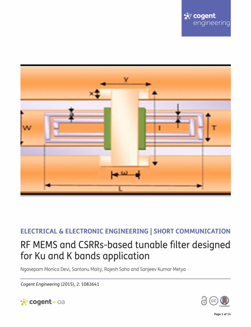
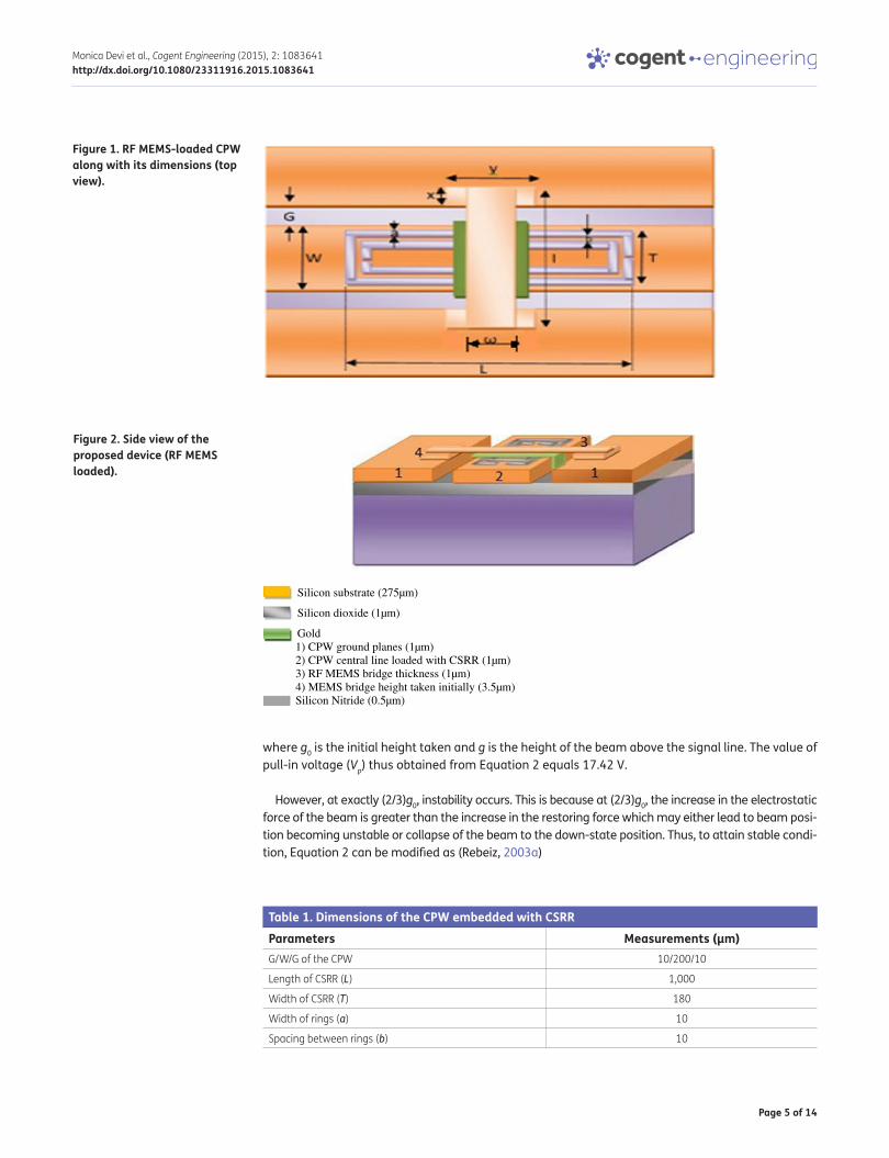
2. Proposed device structureThe top and side view of the proposed device is shown in Figures 1 and 2, respectively. Initially, a copla nar waveguide (CPW) structure made of gold was designed on a high-resistivity silicon substrate. The CPW has a central signal line and two ground plane. On the central line of CPW structure, rectangular-shaped CSRR-embedded (CSRR consists of two split-type concentric structures) was designed. To achieve tunablity in frequency band, MEMS shunt switch has been designed above CPW. Two anchors of the bridge is fixed on ground plane and the metal bridge is suspended over the signal line of CPW. Table 1 shows the different parameters related to design of CPW and CSRR along with their dimen-sions. These dimensions of the device were calculated to achieve proper impedance matching. MEMS bridge is suspended over the signal line with an air gap of g0 and its corresponding parameters related to length, width, and thickness are given in Table 2, respectively. The design parameters are taken from the basic CPW expression to get 50-ohm impedance. So through the impedance matching condi-tion, the CPW parameters and CSRR structures parameters are calculated (shown in Table 1). And to get the low actuation voltage and higher switching speed, different switch parameters shown in Table 2 are calculated from basic switch expression. During actuation, the MEMS beam is 0.5 µm away from the signal line in down-state condition and 3.5 µm for up-state condition. The air-gap height has been chosen as 3 µm for obtaining a higher tuning range. There will be instability of MEMS bridges, if the gap height is less than 2 µm, as the gap becomes less than 2/3 times of original gap (Rebeiz, 2003a). A thin layer of silicon nitride (Si3N4) with a thickness of 0.5 µm is added on top of the central line to prevent the shorting of the CSRR with the MEMS bridge, thereby generating a capacitive effect in the down-state condition. The proposed device is very small in size in comparison to other existing devices.
3. Mechanical propertiesIn this section, the mechanical parameters related to the proposed device have been calculated one by one.
3.1. Spring constant (k)The mechanical behavior can be modeled using a linear spring constant, k (N/m), since the operation of the structure is limited to small deflections. The total spring constant is given by the stiffness of the beam and the biaxial residual stress. Hence, the expression of spring constant is given as follows (Rebeiz, 2003a):
where E is Young’s modulus (E = 80 GPa for gold), σ is residual stress of the beam, and ν is Poisson’s coefficient (ν = 0.42 for gold). In ideal case, when σ = 0 and putting the values of other parameters from Table 2, the value of k obtained is 7.8 N/m.
3.2. Pull-in voltage (Vp)The expression for the pull-in voltage is given as (Rebeiz, 2003a)
(1)k = 32Ew(t∕l)3 + 8�(1 − �)w(t∕l)
(2)Vp =
√
2k
�0Ww
g2(g0− g)
Page 5 of 14
Monica Devi et al., Cogent Engineering (2015), 2: 1083641http://dx.doi.org/10.1080/23311916.2015.1083641
where g0 is the initial height taken and g is the height of the beam above the signal line. The value of pull-in voltage (Vp) thus obtained from Equation 2 equals 17.42 V.
However, at exactly (2/3)g0, instability occurs. This is because at (2/3)g0, the increase in the electrostatic force of the beam is greater than the increase in the restoring force which may either lead to beam posi-tion becoming unstable or collapse of the beam to the down-state position. Thus, to attain stable condi-tion, Equation 2 can be modified as (Rebeiz, 2003a)
Figure 1. RF MEMS-loaded CPW along with its dimensions (top view).
Figure 2. Side view of the proposed device (RF MEMS loaded).
Silicon substrate (275µm)
Silicon dioxide (1µm)
Gold1) CPW ground planes (1µm)2) CPW central line loaded with CSRR (1µm)3) RF MEMS bridge thickness (1µm)4) MEMS bridge height taken initially (3.5µm)Silicon Nitride (0.5µm)
Table 1. Dimensions of the CPW embedded with CSRRParameters Measurements (µm)G/W/G of the CPW 10/200/10
Length of CSRR (L) 1,000
Width of CSRR (T) 180
Width of rings (a) 10
Spacing between rings (b) 10
Page 6 of 14
Monica Devi et al., Cogent Engineering (2015), 2: 1083641http://dx.doi.org/10.1080/23311916.2015.1083641
3.3. Damping coefficient (b) and quality factor (Q.F.)The expression of damping coefficient (b) is given by (Rebeiz, 2003a)
where μ is coefficient of viscosity of ideal gases at standard temperature and pressure (STP) and is equal to 1.85 × 10⁻⁵ Pa-s. Thus, the value of damping coefficient obtained from Equation 4 equals 1.30 × 10⁻⁴.
The expression for the mechanical resonant frequency of beam vibration is given by (Rebeiz, 2003a)
where m is the modal mass of the beam and is given by m = 0.35 × (l × w × t) × ρ = 2.16 × 10⁻¹⁰ kg, (density of gold ρ = 19,320 kg/m3).
The equation of Q.F. for fixed–fixed beam is (Rebeiz, 2003a)
where w0 is the angular frequency of beam vibration. Thus, from Equation 6, the value of Q.F. obtained equals 0.29.
3.4. Beam switching time (ts)The switching time for each beam to complete one up and down cycle is (Rebeiz, 2003a)
where vs equals 1.4vp and w0 is the angular frequency of beam vibration. Thus, the switching time obtained from Equation 7 equals 0.138 µs.
Usually, MEMS devices require high pull-in voltage of the range 30–80 V (Rebeiz, 2003b). However, this proposed device has achieved a reduced pull-in voltage of only 17.42 V. Moreover, the designed device with CPW layers and MEMS bridge made of gold gives a relatively faster switching time of 0.138 µs, which is faster than switching time of conventional electrostatic MEMS switches (Rebeiz, 2003b). Table 3 shows a comparative analysis of three different materials when used as a bridge. From this table, it is seen that Al gives the lowest pull-in voltage and spring constant, whereas Polysilicon provides the highest spring constant and pull-in voltage. Thus, there is a trade-off between the properties for the two materials. Hence, it can be inferred that the overall performance of gold is better as it gives accept-able spring constant and pull-in voltage, better quality factor and faster switching time when compared to Al and Polysilicon.
(3)Vp = V(2∕3)g0 =
√
8k
27�0Ww
g30
(4)b = (3∕2�)(�A2∕g30)
(5)f0= (1∕2�)
√
k∕m
(6)Q.F. =k
w0b=
√
E�t2
�(wl∕2)2g30
(7)ts = 3.67vp∕(vsw0)
Table 2. Dimensions of the MEMS bridge and the anchorParameters Measurements (µm)Length of the MEMS bridge (l) 320
Width of the MEMS bridge (w) 100
Thickness of the MEMS bridge (t) 1
Length of the anchor (x) 50
Width of the anchor (y) 200

Page 7 of 14
Monica Devi et al., Cogent Engineering (2015), 2: 1083641http://dx.doi.org/10.1080/23311916.2015.1083641
4. Device behaviorIn this section, the electromechanical behavior of the device has been shown and analyzed. The proposed structure is designed and simulated using An soft HFSS, a simulator for 3D volumetric pas-sive device modeling. The simulation is carried out for the loaded CPW by considering a bridge height of 3.5 µm for the up state, thus keeping an initial gap height of 3 µm. The air-gap height for the down state is chosen as (2/3)g0, thus considering 2.5 µm as the bridge height. The stop-band frequency response with a reconfigurable capability gives a tuning range of 15%. The device achieves a rejection level of −24 dB at 16.5 GHz in down-state position as depicted in Figure 3. While in Figure 4, which is the up-state position, a notch level of −28.5 dB is obtained at 19.5 GHz when a dielectric thickness of 0.5 µm is given. Therefore, the resonant frequency shifts from 19.5 GHz (K-band) to 16.5 GHz (Ku band) when the switch moves from up to down state.
Figure 3. S-parameters performance of the proposed device in down-state position.
0 5 10 15 20 25 30
-25
-20
-15
-10
-5
0
S-pa
ram
eter
s (d
B)
Frequency (GHz)
S(1,1)S(2,1)
Figure 4. S-parameters performance of the proposed device in up-state position.
0 5 10 15 20 25 30 35
-30
-25
-20
-15
-10
-5
0
S-pa
ram
eter
s (d
B)
Frequency (GHz)
S(1,1)
S(2,1)
Table 3. Comparison of the beam materials with its mechanical propertiesMechanical properties Au Al PolysiliconSpring constant (N/m) 7.8 6.74 16.6
Pull-in voltage (V) 17.42 17.39 27.3
Quality factor 0.29 0.109 0.16
Switching time (µs) 0.138 5.56 3.29
Page 8 of 14
Monica Devi et al., Cogent Engineering (2015), 2: 1083641http://dx.doi.org/10.1080/23311916.2015.1083641
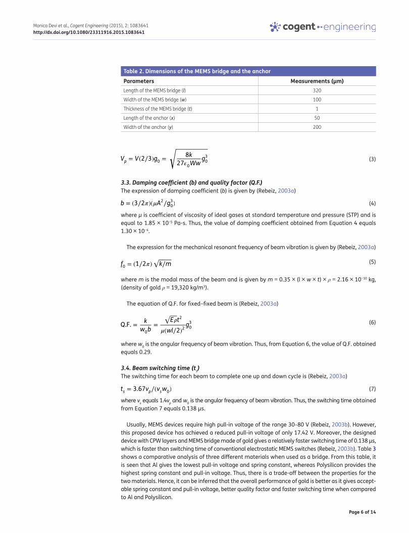
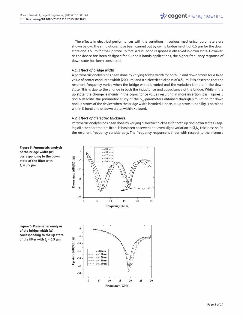
The effects in electrical performances with the variations in various mechanical parameters are shown below. The simulations have been carried out by giving bridge height of 0.5 µm for the down state and 3.5 µm for the up state. In fact, a dual-band response is observed in down state. However, as the device has been designed for Ku and K bands applications, the higher frequency response of down state has been considered.
4.1. Effect of bridge widthA parametric analysis has been done by varying bridge width for both up and down states for a fixed value of center conductor width (200 µm) and a dielectric thickness of 0.5 µm. It is observed that the resonant frequency varies when the bridge width is varied and the variation is more in the down state. This is due to the change in both the inductance and capacitance of the bridge. While in the up state, the change is mainly in the capacitance values resulting in more insertion loss. Figures 5 and 6 describe the parametric study of the S21-parameters obtained through simulation for down and up states of the device when the bridge width is varied. Hence, at up state, tunability is obtained within K band and at down state, within Ku band.
4.2. Effect of dielectric thicknessParametric analysis has been done by varying dielectric thickness for both up and down states keep-ing all other parameters fixed. It has been observed that even slight variation in Si3N4 thickness shifts the resonant frequency considerably. The frequency response is linear with respect to the increase
Figure 5. Parametric analysis of the bridge width (w) corresponding to the down state of the filter with td = 0.5 µm.
-25
-20
-15
-10
-5
0
Dow
n st
ate
(dB
(S(2
,1))
)
Frequency (GHz)
w=80umw=100umw=120umw=140umw=160um
frequency shifted
0 5 10 15 20 25
Figure 6. Parametric analysis of the bridge width (w) corresponding to the up state of the filter with td = 0.5 µm.
0 5 10 15 20 25 30
-30
-25
-20
-15
-10
-5
0
Up
stat
e (d
B(S
(2,1
)))
Frequency (GHz)
w=80umw=100umw=120umw=140umw=160um

Page 9 of 14
Monica Devi et al., Cogent Engineering (2015), 2: 1083641http://dx.doi.org/10.1080/23311916.2015.1083641
in dielectric thickness. However, to obtain a larger bandwidth and maintain a low pull-in voltage, varying the bridge width is favorable. Figures 7 and 8 show the parametric study of the S21-parameters for down and up states of the device designed with the variation of dielectric thickness (td). Therefore, down and up state tunability has been obtained at Ku and K, band respectively. From Figure 9, it can be observed that the frequency changes almost linearly with change in dielectric thickness (td).
Figure 7. Parametric analysis of the dielectric thickness (td) corresponding to the down state of the filter with bridge width (w) = 100 µm.
-20
-15
-10
-5
0D
own
stat
e (S
(2,1
))
Frequency (GHz)
td=0.5um
td=0.6um
td=0.7um
td=0.8um
td=0.9um
td=1umfrequency shifted
0 5 10 15 20 25 30
Figure 8. Parametric analysis of the dielectric thickness (td) corresponding to the up state of the filter with w = 100 µm.
0 5 10 15 20 25 30 35 40
-30
-25
-20
-15
-10
-5
0
Up
stat
e (d
B(S
(2,1
)))
Frequency (GHz)
td=0.5um
td=0.6um
td=0.7um
td=0.8um
td=0.9um
td=1um
Figure 9. Simulated result showing the increase in frequency response with change in dielectric thickness.
0.5 0.6 0.7 0.8 0.9 1.0
16.6
16.8
17.017.2
17.4
17.6
17.8
18.018.2
18.4
18.6
Fre
quen
cy (
GH
z)
Dielectric thickness (td)
Frequency
Page 10 of 14
Monica Devi et al., Cogent Engineering (2015), 2: 1083641http://dx.doi.org/10.1080/23311916.2015.1083641
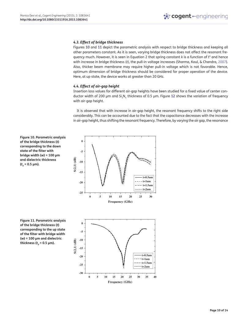
4.3. Effect of bridge thicknessFigures 10 and 11 depict the parametric analysis with respect to bridge thickness and keeping all other parameters constant. As it is seen, varying bridge thickness does not affect the resonant fre-quency much. However, it is seen in Equation 2 that spring constant k is a function of t3 and hence with increase in bridge thickness (t), the pull-in voltage increases (Sharma, Koul, & Chandra, 2007). Also, thicker beam membrane may require higher pull-in voltage which is not favorable. Hence, optimum dimension of bridge thickness should be considered for proper operation of the device. Here, at up state, the device works at greater than 20 GHz.
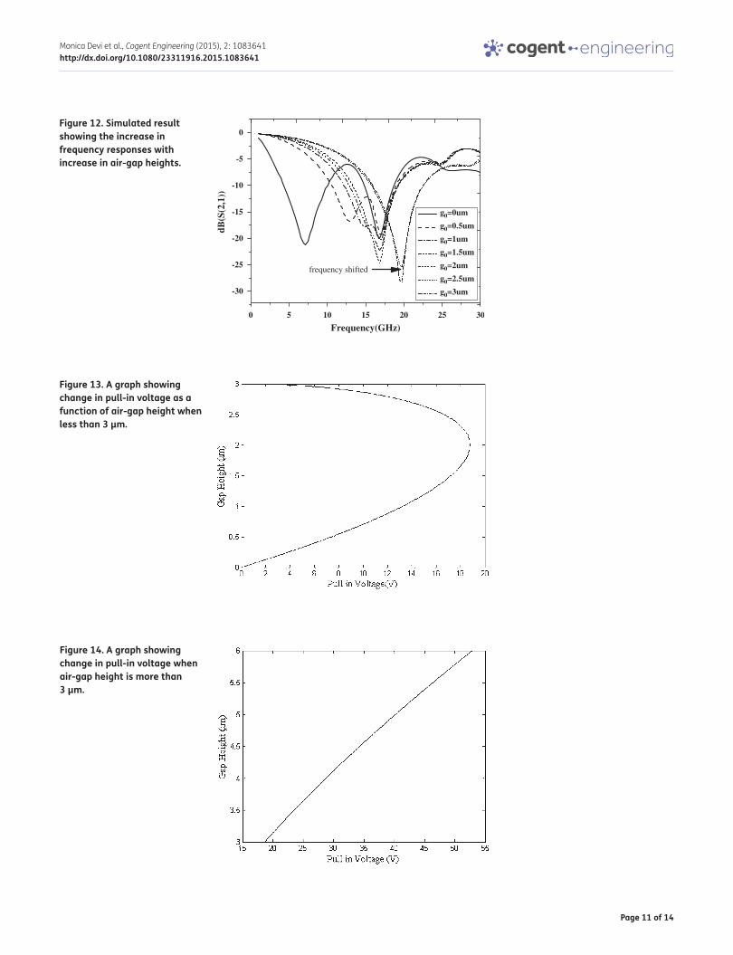
4.4. Effect of air-gap heightInsertion loss values for different air-gap heights have been studied for a fixed value of center con-ductor width of 200 µm and Si3N4 thickness of 0.5 µm. Figure 12 shows the variation of frequency with air-gap height.
It is observed that with increase in air-gap height, the resonant frequency shifts to the right side considerably. This can be accounted due to the fact that the capacitance decreases with the increase in air-gap height, thus shifting the resonant frequency. Therefore, by varying the air gap, the resonance
Figure 10. Parametric analysis of the bridge thickness (t) corresponding to the down state of the filter with bridge width (w) = 100 µm and dielectric thickness (td = 0.5 µm).
-25
-20
-15
-10
-5
0
S(2,
1) (
dB)
Frequency (GHz)
t=0.5umt=1umt=1.5umt=2um
0 5 10 15 20 25 30
Figure 11. Parametric analysis of the bridge thickness (t) corresponding to the up state of the filter with bridge width (w) = 100 µm and dielectric thickness (td = 0.5 µm).
0 5 10 15 20 25 30 35 40-30
-25
-20
-15
-10
-5
0
S(2,
1) (
dB)
Frequency (GHz)
t=0.5umt=1umt=1.5umt=2um
Page 11 of 14
Monica Devi et al., Cogent Engineering (2015), 2: 1083641http://dx.doi.org/10.1080/23311916.2015.1083641
Figure 13. A graph showing change in pull-in voltage as a function of air-gap height when less than 3 µm.
Figure 14. A graph showing change in pull-in voltage when air-gap height is more than 3 µm.
Figure 12. Simulated result showing the increase in frequency responses with increase in air-gap heights.
0 5 10 15 20 25 30
-30
-25
-20
-15
-10
-5
0
dB(S
(2,1
))
Frequency(GHz)
g0=0um
g0=0.5um
g0=1um
g0=1.5um
g0=2um
g0=2.5um
g0=3um
frequency shifted
Page 12 of 14
Monica Devi et al., Cogent Engineering (2015), 2: 1083641http://dx.doi.org/10.1080/23311916.2015.1083641
frequency shifted from Ku to K band. From Figure 13, it can be observed that the pull-in voltage chang-es almost linearly with change in air gap height, which was also indicated in Equation 2. Figure 14 shows the linear change in pull-in voltage when air-gap height is increased from 3 µm.
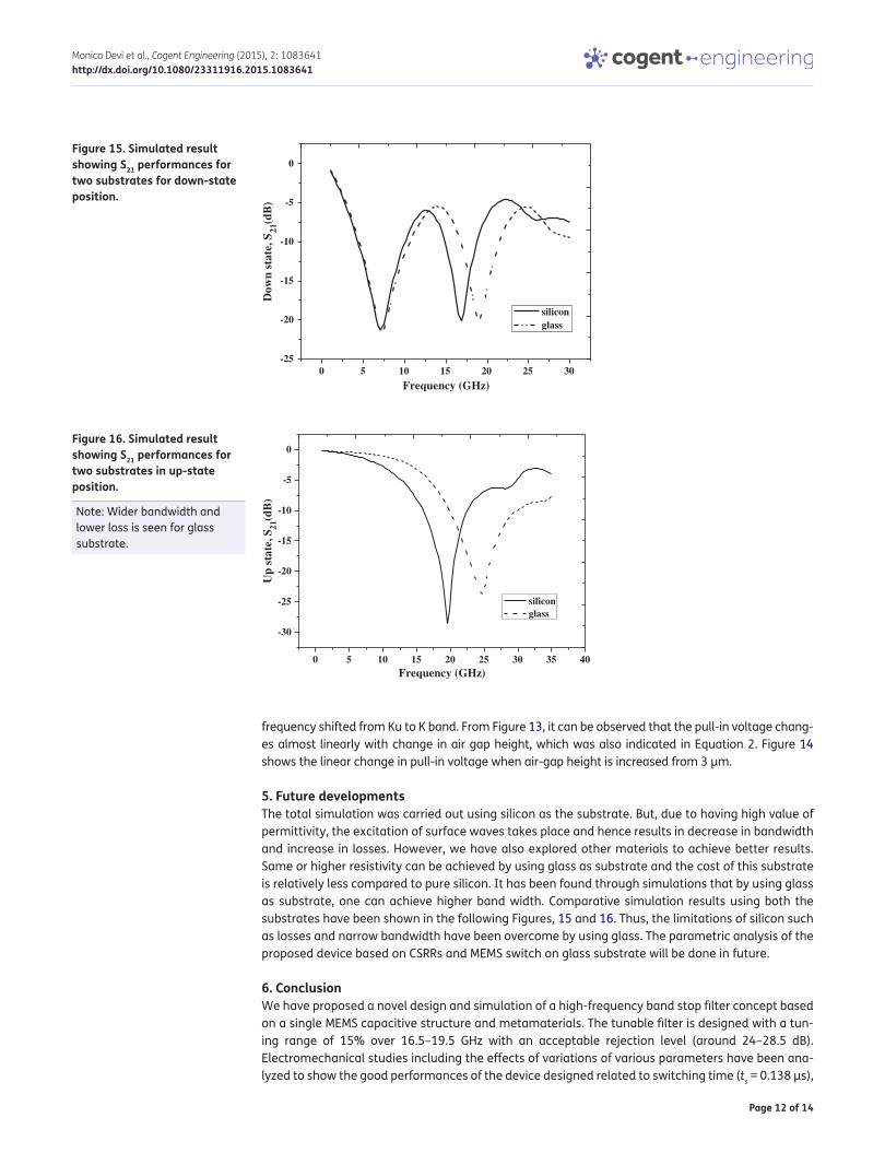
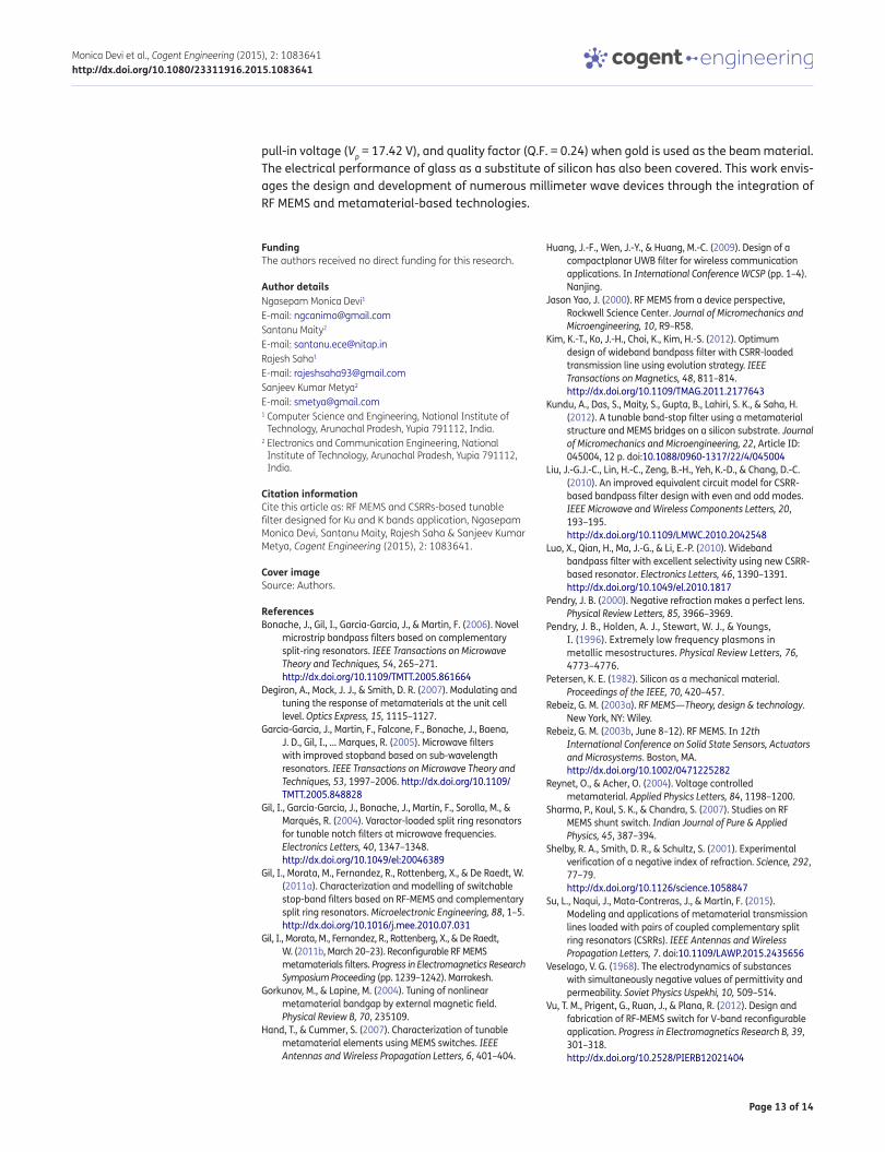
5. Future developmentsThe total simulation was carried out using silicon as the substrate. But, due to having high value of permittivity, the excitation of surface waves takes place and hence results in decrease in bandwidth and increase in losses. However, we have also explored other materials to achieve better results. Same or higher resistivity can be achieved by using glass as substrate and the cost of this substrate is relatively less compared to pure silicon. It has been found through simulations that by using glass as substrate, one can achieve higher band width. Comparative simulation results using both the substrates have been shown in the following Figures, 15 and 16. Thus, the limitations of silicon such as losses and narrow bandwidth have been overcome by using glass. The parametric analysis of the proposed device based on CSRRs and MEMS switch on glass substrate will be done in future.
6. ConclusionWe have proposed a novel design and simulation of a high-frequency band stop filter concept based on a single MEMS capacitive structure and metamaterials. The tunable filter is designed with a tun-ing range of 15% over 16.5–19.5 GHz with an acceptable rejection level (around 24–28.5 dB). Electromechanical studies including the effects of variations of various parameters have been ana-lyzed to show the good performances of the device designed related to switching time (ts = 0.138 µs),
Figure 15. Simulated result showing S21 performances for two substrates for down-state position.
0 5 10 15 20 25 30-25
-20
-15
-10
-5
0
Dow
n st
ate,
S21
(dB
)
Frequency (GHz)
siliconglass
Figure 16. Simulated result showing S21 performances for two substrates in up-state position.
Note: Wider bandwidth and lower loss is seen for glass substrate.
0 5 10 15 20 25 30 35 40
-30
-25
-20
-15
-10
-5
0
Up
stat
e, S
21(d
B)
Frequency (GHz)
siliconglass
Page 13 of 14
Monica Devi et al., Cogent Engineering (2015), 2: 1083641http://dx.doi.org/10.1080/23311916.2015.1083641
pull-in voltage (Vp = 17.42 V), and quality factor (Q.F. = 0.24) when gold is used as the beam material. The electrical performance of glass as a substitute of silicon has also been covered. This work envis-ages the design and development of numerous millimeter wave devices through the integration of RF MEMS and metamaterial-based technologies.
FundingThe authors received no direct funding for this research.
Author detailsNgasepam Monica Devi1
E-mail: [email protected] Maity2
E-mail: [email protected] Saha1
E-mail: [email protected] Kumar Metya2
E-mail: [email protected] Computer Science and Engineering, National Institute of
Technology, Arunachal Pradesh, Yupia 791112, India.2 Electronics and Communication Engineering, National
Institute of Technology, Arunachal Pradesh, Yupia 791112, India.
Citation informationCite this article as: RF MEMS and CSRRs-based tunable filter designed for Ku and K bands application, Ngasepam Monica Devi, Santanu Maity, Rajesh Saha & Sanjeev Kumar Metya, Cogent Engineering (2015), 2: 1083641.
Cover imageSource: Authors.
ReferencesBonache, J., Gil, I., Garcia-Garcia, J., & Martin, F. (2006). Novel
microstrip bandpass filters based on complementary split-ring resonators. IEEE Transactions on Microwave Theory and Techniques, 54, 265–271. http://dx.doi.org/10.1109/TMTT.2005.861664
Degiron, A., Mock, J. J., & Smith, D. R. (2007). Modulating and tuning the response of metamaterials at the unit cell level. Optics Express, 15, 1115–1127.
Garcia-Garcia, J., Martin, F., Falcone, F., Bonache, J., Baena, J. D., Gil, I., … Marques, R. (2005). Microwave filters with improved stopband based on sub-wavelength resonators. IEEE Transactions on Microwave Theory and Techniques, 53, 1997–2006. http://dx.doi.org/10.1109/TMTT.2005.848828
Gil, I., García-García, J., Bonache, J., Martín, F., Sorolla, M., & Marques, R. (2004). Varactor-loaded split ring resonators for tunable notch filters at microwave frequencies. Electronics Letters, 40, 1347–1348. http://dx.doi.org/10.1049/el:20046389
Gil, I., Morata, M., Fernandez, R., Rottenberg, X., & De Raedt, W. (2011a). Characterization and modelling of switchable stop-band filters based on RF-MEMS and complementary split ring resonators. Microelectronic Engineering, 88, 1–5. http://dx.doi.org/10.1016/j.mee.2010.07.031
Gil, I., Morata, M., Fernandez, R., Rottenberg, X., & De Raedt, W. (2011b, March 20–23). Reconfigurable RF MEMS metamaterials filters. Progress in Electromagnetics Research Symposium Proceeding (pp. 1239–1242). Marrakesh.
Gorkunov, M., & Lapine, M. (2004). Tuning of nonlinear metamaterial bandgap by external magnetic field. Physical Review B, 70, 235109.
Hand, T., & Cummer, S. (2007). Characterization of tunable metamaterial elements using MEMS switches. IEEE Antennas and Wireless Propagation Letters, 6, 401–404.
Huang, J.-F., Wen, J.-Y., & Huang, M.-C. (2009). Design of a compactplanar UWB filter for wireless communication applications. In International Conference WCSP (pp. 1–4). Nanjing.
Jason Yao, J. (2000). RF MEMS from a device perspective, Rockwell Science Center. Journal of Micromechanics and Microengineering, 10, R9–R58.
Kim, K.-T., Ko, J.-H., Choi, K., Kim, H.-S. (2012). Optimum design of wideband bandpass filter with CSRR-loaded transmission line using evolution strategy. IEEE Transactions on Magnetics, 48, 811–814. http://dx.doi.org/10.1109/TMAG.2011.2177643
Kundu, A., Das, S., Maity, S., Gupta, B., Lahiri, S. K., & Saha, H. (2012). A tunable band-stop filter using a metamaterial structure and MEMS bridges on a silicon substrate. Journal of Micromechanics and Microengineering, 22, Article ID: 045004, 12 p. doi:10.1088/0960-1317/22/4/045004
Liu, J.-G.J.-C., Lin, H.-C., Zeng, B.-H., Yeh, K.-D., & Chang, D.-C. (2010). An improved equivalent circuit model for CSRR-based bandpass filter design with even and odd modes. IEEE Microwave and Wireless Components Letters, 20, 193–195. http://dx.doi.org/10.1109/LMWC.2010.2042548
Luo, X., Qian, H., Ma, J.-G., & Li, E.-P. (2010). Wideband bandpass filter with excellent selectivity using new CSRR-based resonator. Electronics Letters, 46, 1390–1391. http://dx.doi.org/10.1049/el.2010.1817
Pendry, J. B. (2000). Negative refraction makes a perfect lens. Physical Review Letters, 85, 3966–3969.
Pendry, J. B., Holden, A. J., Stewart, W. J., & Youngs, I. (1996). Extremely low frequency plasmons in metallic mesostructures. Physical Review Letters, 76, 4773–4776.
Petersen, K. E. (1982). Silicon as a mechanical material. Proceedings of the IEEE, 70, 420–457.
Rebeiz, G. M. (2003a). RF MEMS—Theory, design & technology. New York, NY: Wiley.
Rebeiz, G. M. (2003b, June 8–12). RF MEMS. In 12th International Conference on Solid State Sensors, Actuators and Microsystems. Boston, MA. http://dx.doi.org/10.1002/0471225282
Reynet, O., & Acher, O. (2004). Voltage controlled metamaterial. Applied Physics Letters, 84, 1198–1200.
Sharma, P., Koul, S. K., & Chandra, S. (2007). Studies on RF MEMS shunt switch. Indian Journal of Pure & Applied Physics, 45, 387–394.
Shelby, R. A., Smith, D. R., & Schultz, S. (2001). Experimental verification of a negative index of refraction. Science, 292, 77–79. http://dx.doi.org/10.1126/science.1058847
Su, L., Naqui, J., Mata-Contreras, J., & Martín, F. (2015). Modeling and applications of metamaterial transmission lines loaded with pairs of coupled complementary split ring resonators (CSRRs). IEEE Antennas and Wireless Propagation Letters, 7. doi:10.1109/LAWP.2015.2435656
Veselago, V. G. (1968). The electrodynamics of substances with simultaneously negative values of permittivity and permeability. Soviet Physics Uspekhi, 10, 509–514.
Vu, T. M., Prigent, G., Ruan, J., & Plana, R. (2012). Design and fabrication of RF-MEMS switch for V-band reconfigurable application. Progress in Electromagnetics Research B, 39, 301–318. http://dx.doi.org/10.2528/PIERB12021404

Page 14 of 14
Monica Devi et al., Cogent Engineering (2015), 2: 1083641http://dx.doi.org/10.1080/23311916.2015.1083641
© 2015 The Author(s). This open access article is distributed under a Creative Commons Attribution (CC-BY) 4.0 license.You are free to: Share — copy and redistribute the material in any medium or format Adapt — remix, transform, and build upon the material for any purpose, even commercially.The licensor cannot revoke these freedoms as long as you follow the license terms.
Under the following terms:Attribution — You must give appropriate credit, provide a link to the license, and indicate if changes were made. You may do so in any reasonable manner, but not in any way that suggests the licensor endorses you or your use. No additional restrictions You may not apply legal terms or technological measures that legally restrict others from doing anything the license permits.
Cogent Engineering (ISSN: 2331-1916) is published by Cogent OA, part of Taylor & Francis Group. Publishing with Cogent OA ensures:• Immediate, universal access to your article on publication• High visibility and discoverability via the Cogent OA website as well as Taylor & Francis Online• Download and citation statistics for your article• Rapid online publication• Input from, and dialog with, expert editors and editorial boards• Retention of full copyright of your article• Guaranteed legacy preservation of your article• Discounts and waivers for authors in developing regionsSubmit your manuscript to a Cogent OA journal at www.CogentOA.com