Embed Size (px)
Citation preview
Computer Architecture:Main Memory (Part II)
Prof. Onur MutluCarnegie Mellon University
(reorged & cut by Seth)
Review: DRAM Controller: Functions Ensure correct operation of DRAM (refresh and timing)
Service DRAM requests while obeying timing constraints of DRAM chips Constraints: resource conflicts (bank, bus, channel), minimum
write-to-read delays Translate requests to DRAM command sequences
Buffer and schedule requests to improve performance Reordering, row-buffer, bank, rank, bus management
Manage power consumption and thermals in DRAM Turn on/off DRAM chips, manage power modes
2
DRAM Power Management DRAM chips have power modes Idea: When not accessing a chip power it down
Power states Active (highest power) All banks idle Power-down Self-refresh (lowest power)
Tradeoff: State transitions incur latency during which the chip cannot be accessed
3
Review: Why are DRAM Controllers Difficult to Design?
Need to obey DRAM timing constraints for correctness There are many (50+) timing constraints in DRAM tWTR: Minimum number of cycles to wait before issuing a
read command after a write command is issued tRC: Minimum number of cycles between the issuing of two
consecutive activate commands to the same bank …
Need to keep track of many resources to prevent conflicts Channels, banks, ranks, data bus, address bus, row buffers
Need to handle DRAM refresh Need to optimize for performance (in the presence of constraints)
Reordering is not simple Predicting the future?
4
Review: Many DRAM Timing Constraints
From Lee et al., “DRAM-Aware Last-Level Cache Writeback: Reducing Write-Caused Interference in Memory Systems,” HPS Technical Report, April 2010.
5
Review: More on DRAM Operation Kim et al., “A Case for Exploiting Subarray-Level Parallelism
(SALP) in DRAM,” ISCA 2012. Lee et al., “Tiered-Latency DRAM: A Low Latency and Low
Cost DRAM Architecture,” HPCA 2013.
6
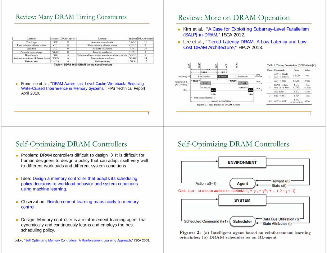
Self-Optimizing DRAM Controllers Problem: DRAM controllers difficult to design It is difficult for
human designers to design a policy that can adapt itself very well to different workloads and different system conditions
Idea: Design a memory controller that adapts its scheduling policy decisions to workload behavior and system conditions using machine learning.
Observation: Reinforcement learning maps nicely to memory control.
Design: Memory controller is a reinforcement learning agent that dynamically and continuously learns and employs the best scheduling policy.
7Ipek+, “Self Optimizing Memory Controllers: A Reinforcement Learning Approach,” ISCA 2008.
Self-Optimizing DRAM Controllers Engin Ipek, Onur Mutlu, José F. Martínez, and Rich
Caruana, "Self Optimizing Memory Controllers: A Reinforcement Learning Approach"Proceedings of the 35th International Symposium on Computer Architecture (ISCA), pages 39-50, Beijing, China, June 2008.
8
Goal: Learn to choose actions to maximize r0 + r1 + 2r2 + … ( 0 < 1)
Self-Optimizing DRAM Controllers Dynamically adapt the memory scheduling policy via
interaction with the system at runtime Associate system states and actions (commands) with long term
reward values Schedule command with highest estimated long-term value in each
state Continuously update state-action values based on feedback from
system
9
Self-Optimizing DRAM Controllers Engin Ipek, Onur Mutlu, José F. Martínez, and Rich Caruana,
"Self Optimizing Memory Controllers: A Reinforcement Learning Approach"Proceedings of the 35th International Symposium on Computer Architecture(ISCA), pages 39-50, Beijing, China, June 2008.
10
States, Actions, Rewards
11
❖ Reward function
• +1 for scheduling Read and Write commands
• 0 at all other times
❖ State attributes
• Number of reads, writes, and load misses in transaction queue
• Number of pending writes and ROB heads waiting for referenced row
• Request’s relative ROB order
❖ Actions
• Activate
• Write
• Read - load miss
• Read - store miss
• Precharge - pending
• Precharge - preemptive
• NOP
Performance Results
12
Self Optimizing DRAM Controllers Advantages
+ Adapts the scheduling policy dynamically to changing workload behavior and to maximize a long-term target+ Reduces the designer’s burden in finding a good scheduling policy. Designer specifies:
1) What system variables might be useful2) What target to optimize, but not how to optimize it
Disadvantages-- Black box: designer much less likely to implement what she cannot easily reason about-- How to specify different reward functions that can achieve different objectives? (e.g., fairness, QoS)
13
Trends Affecting Main Memory
Major Trends Affecting Main Memory (I) Need for main memory capacity, bandwidth, QoS increasing
Main memory energy/power is a key system design concern
DRAM technology scaling is ending
15
Major Trends Affecting Main Memory (II) Need for main memory capacity, bandwidth, QoS increasing
Multi-core: increasing number of cores Data-intensive applications: increasing demand/hunger for data Consolidation: cloud computing, GPUs, mobile
Main memory energy/power is a key system design concern
DRAM technology scaling is ending
16
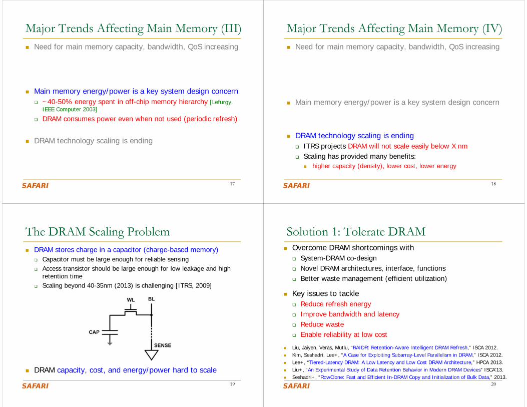
Major Trends Affecting Main Memory (III) Need for main memory capacity, bandwidth, QoS increasing
Main memory energy/power is a key system design concern ~40-50% energy spent in off-chip memory hierarchy [Lefurgy,
IEEE Computer 2003]
DRAM consumes power even when not used (periodic refresh)
DRAM technology scaling is ending
17
Major Trends Affecting Main Memory (IV) Need for main memory capacity, bandwidth, QoS increasing
Main memory energy/power is a key system design concern
DRAM technology scaling is ending ITRS projects DRAM will not scale easily below X nm Scaling has provided many benefits:
higher capacity (density), lower cost, lower energy
18
The DRAM Scaling Problem DRAM stores charge in a capacitor (charge-based memory)
Capacitor must be large enough for reliable sensing Access transistor should be large enough for low leakage and high
retention time Scaling beyond 40-35nm (2013) is challenging [ITRS, 2009]
DRAM capacity, cost, and energy/power hard to scale
19
Solution 1: Tolerate DRAM Overcome DRAM shortcomings with
System-DRAM co-design Novel DRAM architectures, interface, functions Better waste management (efficient utilization)
Key issues to tackle Reduce refresh energy Improve bandwidth and latency Reduce waste Enable reliability at low cost
Liu, Jaiyen, Veras, Mutlu, “RAIDR: Retention-Aware Intelligent DRAM Refresh,” ISCA 2012. Kim, Seshadri, Lee+, “A Case for Exploiting Subarray-Level Parallelism in DRAM,” ISCA 2012. Lee+, “Tiered-Latency DRAM: A Low Latency and Low Cost DRAM Architecture,” HPCA 2013. Liu+, “An Experimental Study of Data Retention Behavior in Modern DRAM Devices” ISCA’13. Seshadri+, “RowClone: Fast and Efficient In-DRAM Copy and Initialization of Bulk Data,” 2013.
20
Tolerating DRAM:System-DRAM Co-Design
New DRAM Architectures
RAIDR: Reducing Refresh Impact TL-DRAM: Reducing DRAM Latency SALP: Reducing Bank Conflict Impact RowClone: Fast Bulk Data Copy and Initialization
22
RAIDR: Reducing DRAM Refresh Impact
DRAM Refresh DRAM capacitor charge leaks over time
The memory controller needs to refresh each row periodically to restore charge Activate + precharge each row every N ms Typical N = 64 ms
Downsides of refresh-- Energy consumption: Each refresh consumes energy-- Performance degradation: DRAM rank/bank unavailable while
refreshed-- QoS/predictability impact: (Long) pause times during refresh-- Refresh rate limits DRAM density scaling
24

Refresh Today: Auto Refresh
25
Columns
Row
s
Row Buffer
DRAM CONTROLLER
DRAM Bus
BANK 0 BANK 1 BANK 2 BANK 3
A batch of rows are periodically refreshedvia the auto-refresh command
Refresh Overhead: Performance
26
8%
46%
Refresh Overhead: Energy
27
15%
47%
Problem with Conventional Refresh Today: Every row is refreshed at the same rate
Observation: Most rows can be refreshed much less often without losing data [Kim+, EDL’09]
Problem: No support in DRAM for different refresh rates per row
28
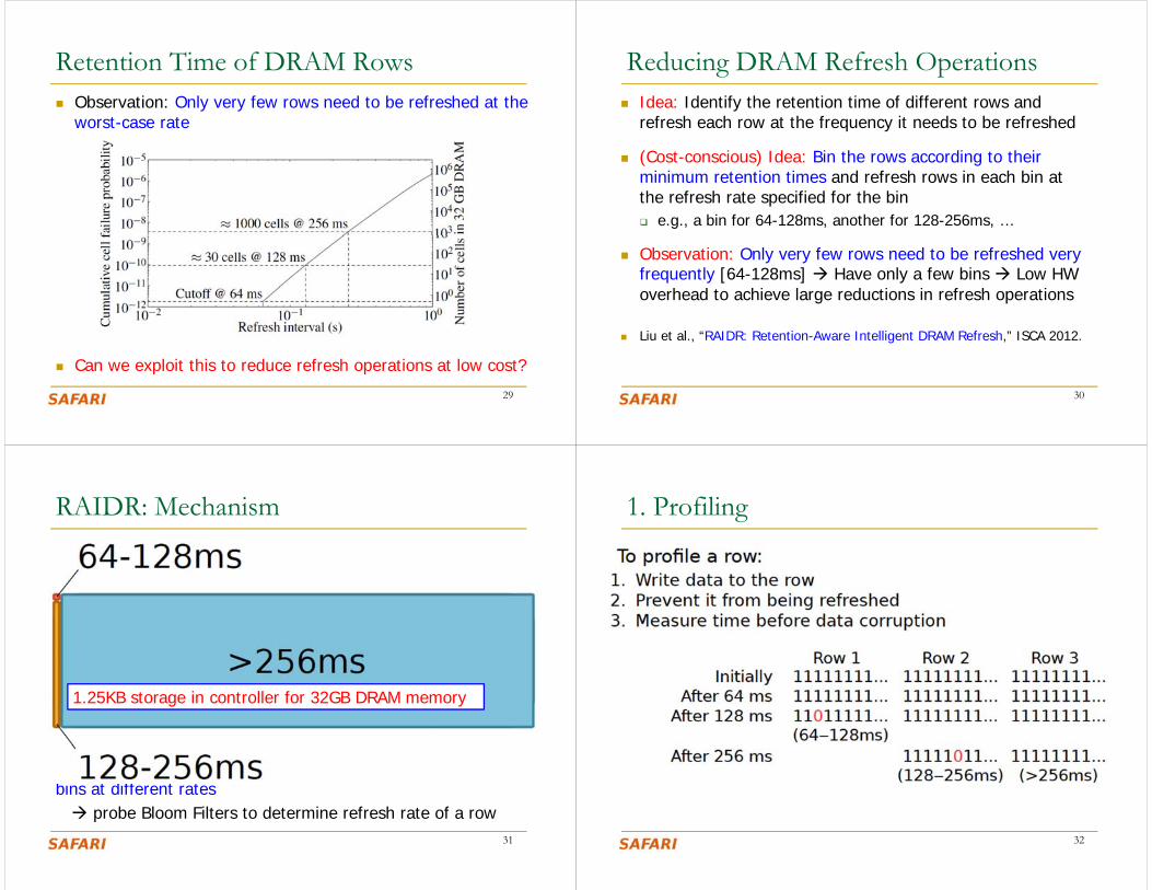
Retention Time of DRAM Rows Observation: Only very few rows need to be refreshed at the
worst-case rate
Can we exploit this to reduce refresh operations at low cost?
29
Reducing DRAM Refresh Operations Idea: Identify the retention time of different rows and
refresh each row at the frequency it needs to be refreshed
(Cost-conscious) Idea: Bin the rows according to their minimum retention times and refresh rows in each bin at the refresh rate specified for the bin e.g., a bin for 64-128ms, another for 128-256ms, …
Observation: Only very few rows need to be refreshed very frequently [64-128ms] Have only a few bins Low HW overhead to achieve large reductions in refresh operations
Liu et al., “RAIDR: Retention-Aware Intelligent DRAM Refresh,” ISCA 2012.
30
1. Profiling: Profile the retention time of all DRAM rows can be done at DRAM design time or dynamically
2. Binning: Store rows into bins by retention time use Bloom Filters for efficient and scalable storage
3. Refreshing: Memory controller refreshes rows in different bins at different rates probe Bloom Filters to determine refresh rate of a row
RAIDR: Mechanism
31
1.25KB storage in controller for 32GB DRAM memory
1. Profiling
32

2. Binning How to efficiently and scalably store rows into retention
time bins? Use Hardware Bloom Filters [Bloom, CACM 1970]
33
Bloom Filter Operation Example
34
Bloom Filter Operation Example
35
Bloom Filter Operation Example
36

Bloom Filter Operation Example
37
Benefits of Bloom Filters as Bins False positives: a row may be declared present in the
Bloom filter even if it was never inserted Not a problem: Refresh some rows more frequently than
needed
No false negatives: rows are never refreshed less frequently than needed (no correctness problems)
Scalable: a Bloom filter never overflows (unlike a fixed-size table)
Efficient: No need to store info on a per-row basis; simple hardware 1.25 KB for 2 filters for 32 GB DRAM system
38
3. Refreshing (RAIDR Refresh Controller)
39
3. Refreshing (RAIDR Refresh Controller)
40
Liu et al., “RAIDR: Retention-Aware Intelligent DRAM Refresh,” ISCA 2012.

Tolerating Temperature Changes
41
RAIDR: Baseline Design
42
Refresh control is in DRAM in today’s auto-refresh systemsRAIDR can be implemented in either the controller or DRAM
RAIDR in Memory Controller: Option 1
43
Overhead of RAIDR in DRAM controller:1.25 KB Bloom Filters, 3 counters, additional commands issued for per-row refresh (all accounted for in evaluations)
RAIDR in DRAM Chip: Option 2
44
Overhead of RAIDR in DRAM chip:Per-chip overhead: 20B Bloom Filters, 1 counter (4 Gbit chip)
Total overhead: 1.25KB Bloom Filters, 64 counters (32 GB DRAM)

RAIDR Results Baseline:
32 GB DDR3 DRAM system (8 cores, 512KB cache/core) 64ms refresh interval for all rows
RAIDR: 64–128ms retention range: 256 B Bloom filter, 10 hash functions 128–256ms retention range: 1 KB Bloom filter, 6 hash functions Default refresh interval: 256 ms
Results on SPEC CPU2006, TPC-C, TPC-H benchmarks 74.6% refresh reduction ~16%/20% DRAM dynamic/idle power reduction ~9% performance improvement
45
RAIDR Refresh Reduction
46
32 GB DDR3 DRAM system
RAIDR: Performance
47
RAIDR performance benefits increase with workload’s memory intensity
RAIDR: DRAM Energy Efficiency
48
RAIDR energy benefits increase with memory idleness
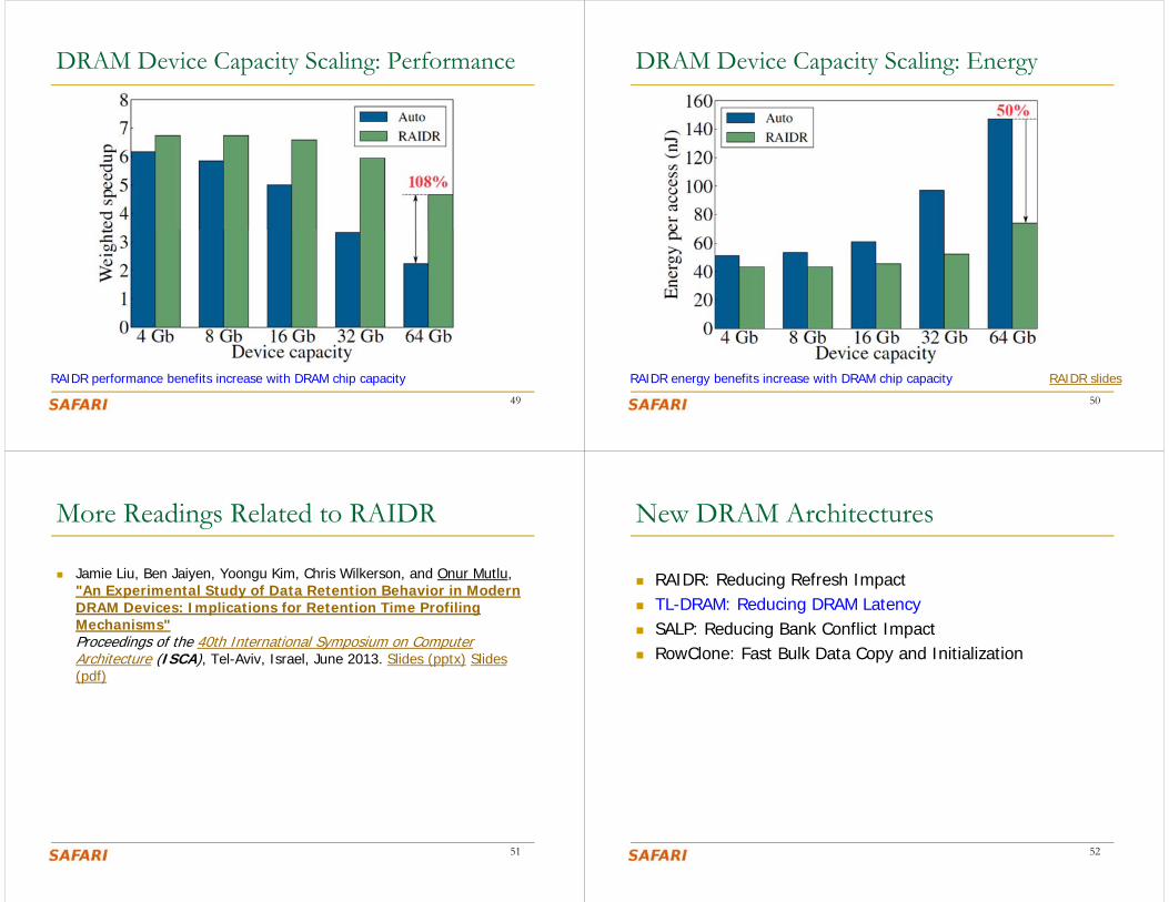
DRAM Device Capacity Scaling: Performance
49
RAIDR performance benefits increase with DRAM chip capacity
DRAM Device Capacity Scaling: Energy
50
RAIDR energy benefits increase with DRAM chip capacity RAIDR slides
More Readings Related to RAIDR
Jamie Liu, Ben Jaiyen, Yoongu Kim, Chris Wilkerson, and Onur Mutlu,"An Experimental Study of Data Retention Behavior in Modern DRAM Devices: Implications for Retention Time Profiling Mechanisms"Proceedings of the 40th International Symposium on Computer Architecture (ISCA), Tel-Aviv, Israel, June 2013. Slides (pptx) Slides (pdf)
51
New DRAM Architectures
RAIDR: Reducing Refresh Impact TL-DRAM: Reducing DRAM Latency SALP: Reducing Bank Conflict Impact RowClone: Fast Bulk Data Copy and Initialization
52

Tiered-Latency DRAM: Reducing DRAM Latency
Donghyuk Lee, Yoongu Kim, Vivek Seshadri, Jamie Liu, Lavanya Subramanian, and Onur Mutlu,"Tiered-Latency DRAM: A Low Latency and Low Cost DRAM Architecture"19th International Symposium on High-Performance Computer Architecture (HPCA),
Shenzhen, China, February 2013. Slides (pptx)
54
Historical DRAM Latency‐Capacity Trend
0
20
40
60
80
100
0.0
0.5
1.0
1.5
2.0
2.5
2000 2003 2006 2008 2011
Latency (ns)
Capa
city (G
b)
Year
Capacity Latency (tRC)
16X
‐20%
DRAM latency continues to be a critical bottleneck
55
What Causes the Long Latency?DRAM Chip
channel
I/O
channel
I/O
cell arraycell array
bankssubarray
subarray
row decod
er
sense amplifier
capacitor
accesstransistor
wordline
bitline
cell
56
DRAM Chip
channel
I/O
channel
I/O
cell arraycell array
bankssubarray
subarrayWhat Causes the Long Latency?
DRAM Latency = Subarray Latency + I/O LatencyDRAM Latency = Subarray Latency + I/O Latency
DominantSuba
rray
I/O
row add
r.
row decoder
sense am
plifier
muxcolumnaddr.
57
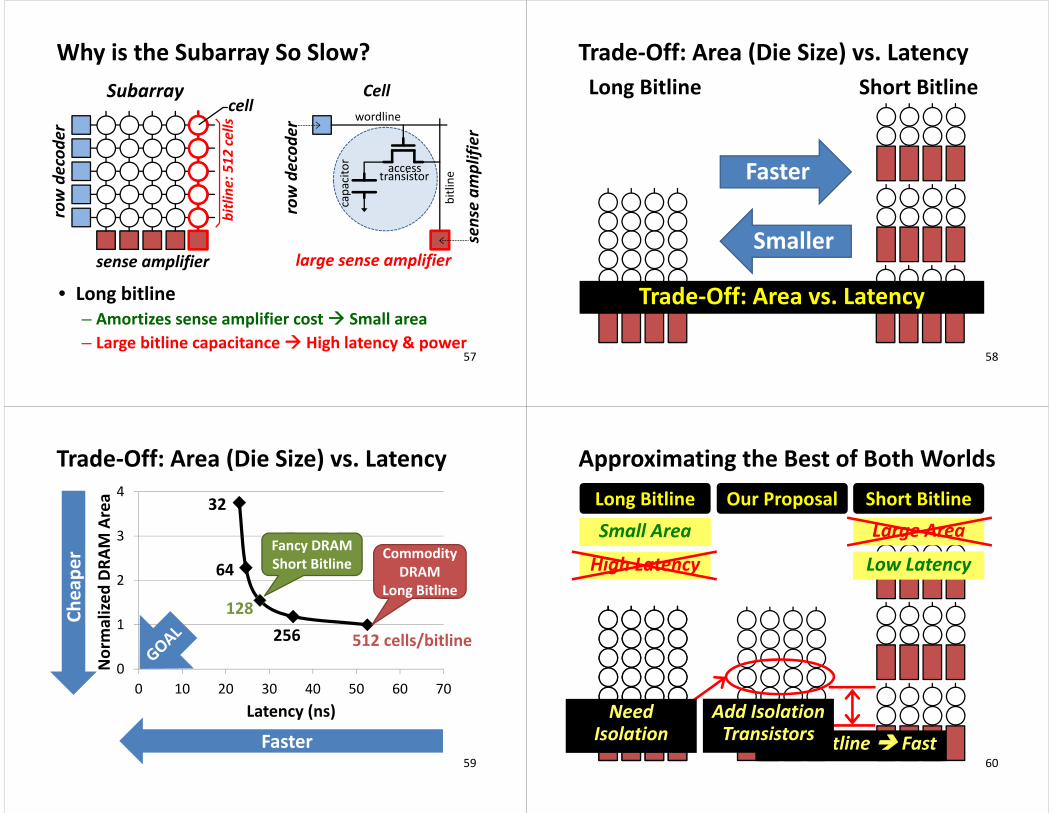
Why is the Subarray So Slow?Subarray
row decod
er
sense amplifier
capacitor
accesstransistor
wordline
bitline
Cell
large sense amplifier
bitline
: 512
cells
cell
• Long bitline– Amortizes sense amplifier cost Small area– Large bitline capacitance High latency & power
sense am
plifier
row decod
er
58
Trade‐Off: Area (Die Size) vs. Latency
Faster
Smaller
Short BitlineLong Bitline
Trade‐Off: Area vs. Latency
59
Trade‐Off: Area (Die Size) vs. Latency
0
1
2
3
4
0 10 20 30 40 50 60 70
Normalize
d DR
AM Area
Latency (ns)
64
32
128256 512 cells/bitline
Commodity DRAM
Long Bitline
Cheape
r
Faster
Fancy DRAMShort Bitline
60
Short Bitline
Low Latency
Approximating the Best of Both WorldsLong BitlineSmall Area Long Bitline
Low Latency
Short BitlineOur ProposalSmall Area
Short Bitline FastNeed
IsolationAdd Isolation Transistors
High Latency
Large Area

61
Approximating the Best of Both Worlds
Low Latency
Our ProposalSmall Area
Long BitlineSmall Area Long Bitline
High Latency
Short Bitline
Low Latency
Short BitlineLarge Area
Tiered‐Latency DRAM
Low Latency
Small area using long bitline
62
Tiered‐Latency DRAM
Near Segment
Far Segment
Isolation Transistor
• Divide a bitline into two segments with an isolation transistor
Sense Amplifier
63
Far SegmentFar Segment
Near Segment Access
Near Segment
Isolation Transistor
• Turn off the isolation transistor
Isolation Transistor (off)
Sense Amplifier
Reduced bitline capacitance Low latency & low power
Reduced bitline length
64
Near SegmentNear Segment
Far Segment Access• Turn on the isolation transistor
Far Segment
Isolation TransistorIsolation Transistor (on)
Sense Amplifier
Large bitline capacitanceAdditional resistance of isolation transistor
Long bitline length
High latency & high power

65
Latency, Power, and Area Evaluation• Commodity DRAM: 512 cells/bitline• TL‐DRAM: 512 cells/bitline
– Near segment: 32 cells– Far segment: 480 cells
• Latency Evaluation– SPICE simulation using circuit‐level DRAM model
• Power and Area Evaluation– DRAM area/power simulator from Rambus– DDR3 energy calculator from Micron
66
0%
50%
100%
150%
0%
50%
100%
150%
Commodity DRAM vs. TL‐DRAM
Latency
Power
–56%
+23%
–51%
+49%• DRAM Latency (tRC) • DRAM Power
• DRAM Area Overhead~3%: mainly due to the isolation transistors
TL‐DRAMCommodity
DRAMNear Far Commodity
DRAMNear FarTL‐DRAM
(52.5ns)
67
Latency vs. Near Segment Length
0
20
40
60
80
1 2 4 8 16 32 64 128 256 512
Near Segment Length (Cells) Ref.
Near Segment Far Segment
Latency (ns)
Longer near segment length leads to higher near segment latency 68
Latency vs. Near Segment Length
0
20
40
60
80
1 2 4 8 16 32 64 128 256 512
Near Segment Length (Cells) Ref.
Near Segment Far Segment
Latency (ns)
Far segment latency is higher than commodity DRAM latency
Far Segment Length = 512 – Near Segment Length
69
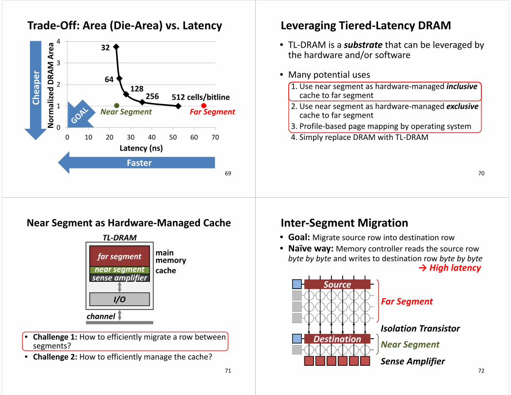
Trade‐Off: Area (Die‐Area) vs. Latency
0
1
2
3
4
0 10 20 30 40 50 60 70
Normalize
d DR
AM Area
Latency (ns)
64
32
128256 512 cells/bitlineCh
eape
r
Faster
Near Segment Far Segment
70
Leveraging Tiered‐Latency DRAM• TL‐DRAM is a substrate that can be leveraged by the hardware and/or software
• Many potential uses1. Use near segment as hardware‐managed inclusivecache to far segment
2. Use near segment as hardware‐managed exclusivecache to far segment
3. Profile‐based page mapping by operating system4. Simply replace DRAM with TL‐DRAM
71
subarray
Near Segment as Hardware‐Managed CacheTL‐DRAM
I/O
cache
mainmemory
• Challenge 1: How to efficiently migrate a row between segments?
• Challenge 2: How to efficiently manage the cache?
far segmentnear segmentsense amplifier
channel
72
Inter‐Segment Migration
Near Segment
Far Segment
Isolation Transistor
Sense Amplifier
Source
Destination
• Goal: Migrate source row into destination row• Naïve way: Memory controller reads the source row byte by byte and writes to destination row byte by byte
→ High latency

73
Inter‐Segment Migration• Our way:
– Source and destination cells share bitlines– Transfer data from source to destination across shared bitlines concurrently
Near Segment
Far Segment
Isolation Transistor
Sense Amplifier
Source
Destination
74
Inter‐Segment Migration
Near Segment
Far Segment
Isolation Transistor
Sense Amplifier
• Our way: – Source and destination cells share bitlines– Transfer data from source to destination acrossshared bitlines concurrently
Step 2: Activate destination row to connect cell and bitline
Step 1: Activate source row
Additional ~4ns over row access latencyMigration is overlapped with source row access
75
subarray
Near Segment as Hardware‐Managed CacheTL‐DRAM
I/O
cache
mainmemory
• Challenge 1: How to efficiently migrate a row between segments?
• Challenge 2: How to efficiently manage the cache?
far segmentnear segmentsense amplifier
channel
76
Evaluation Methodology• System simulator
– CPU: Instruction‐trace‐based x86 simulator– Memory: Cycle‐accurate DDR3 DRAM simulator
• Workloads– 32 Benchmarks from TPC, STREAM, SPEC CPU2006
• Performance Metrics– Single‐core: Instructions‐Per‐Cycle– Multi‐core: Weighted speedup
77
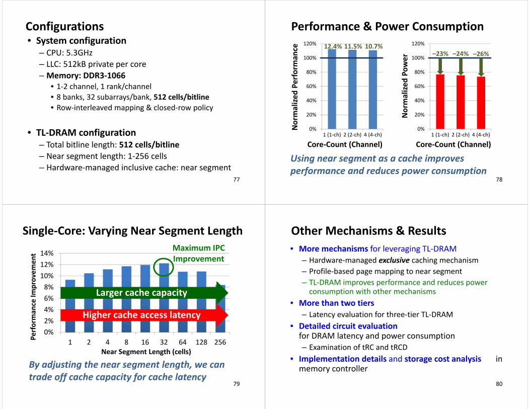
Configurations• System configuration
– CPU: 5.3GHz– LLC: 512kB private per core– Memory: DDR3‐1066
• 1‐2 channel, 1 rank/channel• 8 banks, 32 subarrays/bank, 512 cells/bitline• Row‐interleaved mapping & closed‐row policy
• TL‐DRAM configuration– Total bitline length: 512 cells/bitline– Near segment length: 1‐256 cells– Hardware‐managed inclusive cache: near segment
78
0%
20%
40%
60%
80%
100%
120%
1 (1‐ch) 2 (2‐ch) 4 (4‐ch)0%
20%
40%
60%
80%
100%
120%
1 (1‐ch) 2 (2‐ch) 4 (4‐ch)
Performance & Power Consumption 11.5%
Normalize
d Pe
rforman
ce
Core‐Count (Channel)
Normalize
d Po
wer
Core‐Count (Channel)
10.7%12.4%–23% –24% –26%
Using near segment as a cache improves performance and reduces power consumption
79
0%2%4%6%8%
10%12%14%
1 2 4 8 16 32 64 128 256
Single‐Core: Varying Near Segment Length
By adjusting the near segment length, we can trade off cache capacity for cache latency
Larger cache capacity
Higher cache access latency
Maximum IPC Improvement
Performan
ce Im
provem
ent
Near Segment Length (cells)
80
Other Mechanisms & Results• More mechanisms for leveraging TL‐DRAM
– Hardware‐managed exclusive caching mechanism– Profile‐based page mapping to near segment– TL‐DRAM improves performance and reduces power consumption with other mechanisms
• More than two tiers– Latency evaluation for three‐tier TL‐DRAM
• Detailed circuit evaluationfor DRAM latency and power consumption– Examination of tRC and tRCD
• Implementation details and storage cost analysis in memory controller
81
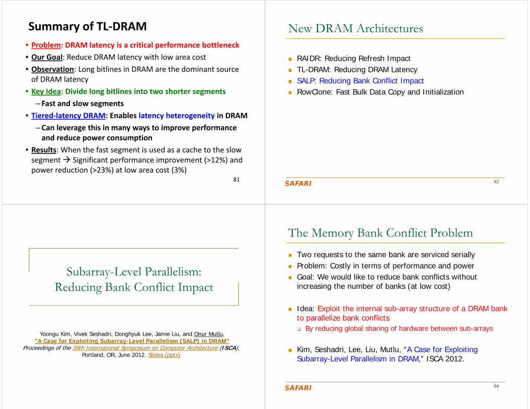
Summary of TL‐DRAM• Problem: DRAM latency is a critical performance bottleneck • Our Goal: Reduce DRAM latency with low area cost• Observation: Long bitlines in DRAM are the dominant source of DRAM latency
• Key Idea: Divide long bitlines into two shorter segments–Fast and slow segments
• Tiered‐latency DRAM: Enables latency heterogeneity in DRAM–Can leverage this in many ways to improve performance and reduce power consumption
• Results: When the fast segment is used as a cache to the slow segment Significant performance improvement (>12%) and power reduction (>23%) at low area cost (3%)
New DRAM Architectures
RAIDR: Reducing Refresh Impact TL-DRAM: Reducing DRAM Latency SALP: Reducing Bank Conflict Impact RowClone: Fast Bulk Data Copy and Initialization
82
Subarray-Level Parallelism:Reducing Bank Conflict Impact
Yoongu Kim, Vivek Seshadri, Donghyuk Lee, Jamie Liu, and Onur Mutlu,"A Case for Exploiting Subarray-Level Parallelism (SALP) in DRAM"
Proceedings of the 39th International Symposium on Computer Architecture (ISCA), Portland, OR, June 2012. Slides (pptx)
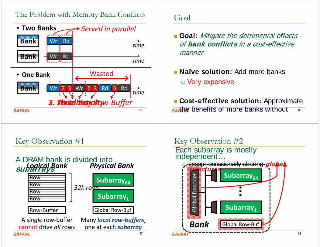
The Memory Bank Conflict Problem Two requests to the same bank are serviced serially Problem: Costly in terms of performance and power Goal: We would like to reduce bank conflicts without
increasing the number of banks (at low cost)
Idea: Exploit the internal sub-array structure of a DRAM bank to parallelize bank conflicts By reducing global sharing of hardware between sub-arrays
Kim, Seshadri, Lee, Liu, Mutlu, “A Case for Exploiting Subarray-Level Parallelism in DRAM,” ISCA 2012.
84
85
timeWr Rd
Wr Rdtime
Bank
time
Bank
Bank
• Two Banks
• One Bank
1. Serialization
Wr Wr Rd RdWr 2 Wr 2 Rd RdWr 2 Wr 2 Rd Rd3 3 3
2. Write Penalty3. Thrashing Row‐Buffer
Served in parallel
Wasted
The Problem with Memory Bank Conflicts Goal
Goal: Mitigate the detrimental effects of bank conflicts in a cost-effective manner
Naïve solution: Add more banks Very expensive
Cost-effective solution: Approximate the benefits of more banks without 86
A DRAM bank is divided into subarrays
Key Observation #1
87
Row
Row‐Buffer
RowRowRow
32k rows
Logical Bank
A single row‐buffer cannot drive all rows
Global Row‐Buf
Physical Bank
Local Row‐Buf
Local Row‐BufSubarray1
Subarray64
Many local row‐buffers, one at each subarray
Key Observation #2Each subarray is mostly independent…
except occasionally sharing global structures
88
Global Row‐Buf
Glob
al Decod
er
Bank
Local Row‐Buf
Local Row‐BufSubarray1
Subarray64
∙∙∙
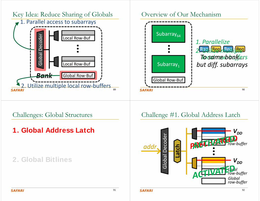
Key Idea: Reduce Sharing of Globals
89
Global Row‐Buf
Glob
al Decod
er
Bank
Local Row‐Buf
Local Row‐Buf
∙∙∙
1. Parallel access to subarrays
2. Utilize multiple local row‐buffers
Overview of Our Mechanism
90
∙∙∙ ReqReq
Global Row‐Buf
Local Row‐Buf
Req
Local Row‐Buf
Req1. Parallelize2. Utilize multiple local row‐buffers
Subarray64
Subarray1To same bank...
but diff. subarrays
Challenges: Global Structures
1. Global Address Latch
2. Global Bitlines
91
Localrow‐buffer
Localrow‐bufferGlobalrow‐buffer
Challenge #1. Global Address Latch
92
∙∙∙addr
VDD
addr
Glob
al Decod
erVDD
Latch
Latch
Latch
Localrow‐buffer
Localrow‐bufferGlobalrow‐buffer
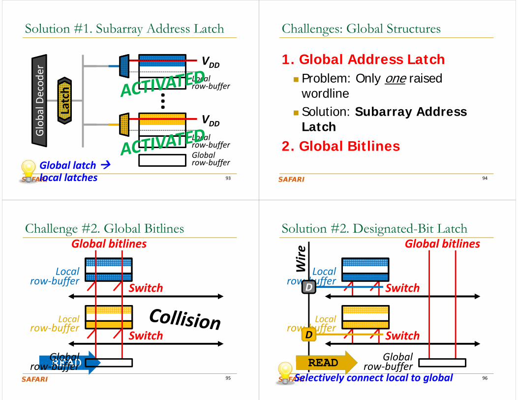
Solution #1. Subarray Address Latch
93
∙∙∙
VDD
Glob
al Decod
er
VDD
Latch
Latch
Latch
Global latch local latches
Challenges: Global Structures
1. Global Address Latch Problem: Only one raised
wordline Solution: Subarray Address
Latch2. Global Bitlines
94
Challenge #2. Global Bitlines
95
Localrow‐buffer
Local row‐buffer
Switch
Switch
READ
Global bitlines
Global row‐buffer
Wire
Solution #2. Designated-Bit Latch
96
Global bitlines
Global row‐buffer
Localrow‐buffer
Local row‐buffer
Switch
Switch
READREAD
DD
DD
Selectively connect local to global

Challenges: Global Structures1. Global Address Latch Problem: Only one raised
wordline Solution: Subarray Address
Latch2. Global Bitlines Problem: Collision during access Solution: Designated-Bit Latch 97
MASA (Multitude of Activated Subarrays)
Baseline (Subarray-Oblivious)
MASA
MASA: Advantages
98
timeWr 2 Wr 2 Rd Rd3 3 3
1. Serialization
2. Write Penalty 3. Thrashing
timeWr
Wr
Rd
Rd
Saved
MASA: Overhead
DRAM Die Size: 0.15% increase Subarray Address Latches Designated-Bit Latches & Wire
DRAM Static Energy: Small increase 0.56mW for each activated subarray But saves dynamic energy
Controller: Small additional storage Keep track of subarray status (< 256B) Keep track of new timing constraints 99
Cheaper Mechanisms
100
D
D
Latches
1. Serialization
2. W
r‐Penalty
3. Thrashing
MASA
SALP‐2
SALP‐1
System Configuration
System Configuration CPU: 5.3GHz, 128 ROB, 8 MSHR LLC: 512kB per-core slice
Memory Configuration DDR3-1066 (default) 1 channel, 1 rank, 8 banks, 8 subarrays-per-
bank (sensitivity) 1-8 chans, 1-8 ranks, 8-64 banks, 1-128 subarrays
Mapping & Row-Policy (default) Line-interleaved & Closed-row (sensitivity) Row-interleaved & Open-row
DRAM Controller Configuration 64-/64-entry read/write queues per-channel FR-FCFS, batch scheduling for writes 101
SALP: Single-core Results
102
0%10%20%30%40%50%60%70%80%
IPC
Im
prov
emen
t MASA "Ideal"
17%
20%
MASA achieves most of the benefit of having more banks (“Ideal”)
SALP: Single-Core Results
103
0%10%20%30%
Incr
ease
SALP-1 SALP-2MASA "Ideal"
SALP‐1, SALP‐2, MASA improve performance at low cost
20%17%13%7%
DRAM Die
Area< 0.15% 0.15
%36.3%
Subarray-Level Parallelism: Results
104
0.00.20.40.60.81.01.2
Nor
mal
ized
D
ynam
ic E
nerg
y
Baseline MASA
0%
20%
40%
60%
80%
100%
Row
-Buf
fer
Hit
-R
ate
Baseline MASA
MASA increases energy-efficiency
- 19 % +13 %

New DRAM Architectures
RAIDR: Reducing Refresh Impact TL-DRAM: Reducing DRAM Latency SALP: Reducing Bank Conflict Impact RowClone: Fast Bulk Data Copy and Initialization
105
RowClone: Fast Bulk Data Copy and Initialization
Vivek Seshadri, Yoongu Kim, Chris Fallin, Donghyuk Lee, Rachata Ausavarungnirun, Gennady Pekhimenko, Yixin Luo, Onur Mutlu, Phillip B. Gibbons, Michael A. Kozuch, Todd C. Mowry,
"RowClone: Fast and Efficient In-DRAM Copy and Initialization of Bulk Data"CMU Computer Science Technical Report, CMU-CS-13-108, Carnegie Mellon University, April 2013.
Today’s Memory: Bulk Data Copy
Memory
MCL3L2L1CPU
1) High latency
2) High bandwidth utilization
3) Cache pollution
4) Unwanted data movement
107
Future: RowClone (In-Memory Copy)
Memory
MCL3L2L1CPU
1) Low latency
2) Low bandwidth utilization
3) No cache pollution
4) No unwanted data movement
108Seshadri et al., “RowClone: Fast and Efficient In-DRAM Copy and Initialization of Bulk Data,” CMU Tech Report 2013.
DRAM operation (load one byte)
Row Buffer (4 Kbits)
Memory Bus
Data pins (8 bits)
DRAM array
4 Kbits
1. Activate row
2. Transferrow
3. Transferbyte onto bus
RowClone: in-DRAM Row Copy (and Initialization)
Row Buffer (4 Kbits)
Memory Bus
Data pins (8 bits)
DRAM array
4 Kbits
1. Activate row A
2. Transferrow
3. Activate row B
4.Transferrow
RowClone: Key Idea
DRAM banks contain1. Mutiple rows of DRAM cells – row = 8KB2. A row buffer shared by the DRAM rows
Large scale copy1. Copy data from source row to row buffer2. Copy data from row buffer to destination row
Can be accomplished by two consecutive ACTIVATEs(if source and destination rows are in the same subarray)
111
RowClone: Intra-subarray Copy
0 1 0 0 1 1 0 0 0 1 1 0
1 1 0 1 0 1 1 1 0 0 1 1
Activate (src) Deactivate (our proposal)
Activate (dst)
0 1 0 0 1 1 0 0 0 1 1 0
? ? ? ? ? ? ? ? ? ? ? ?0 1 0 0 1 1 0 0 0 1 1 0
Sense Amplifiers(row buffer)
src
dst
112

RowClone: Inter-bank Copy
I/O BusTransfer
(our proposal)
src
dst
Read Write
113
RowClone: Inter-subarray Copy
I/O Bus1. Transfer (src to temp)
src
dst
temp
2. Transfer (temp to dst)114
Fast Row Initialization
0 0 0 0 0 0 0 0 0 0 0 0
Fix a row at Zero(0.5% loss in capacity)
115
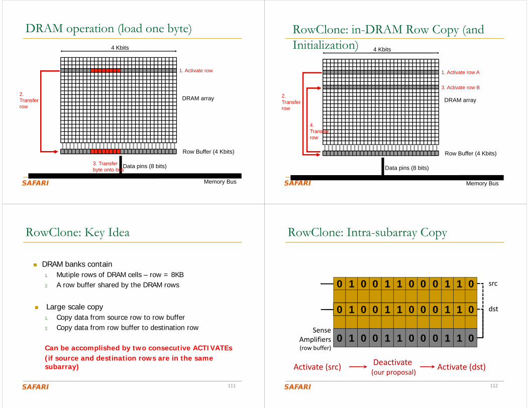
RowClone: Latency and Energy Savings
0
0.2
0.4
0.6
0.8
1
1.2
Latency Energy
Nor
mal
ized
Sav
ings
Baseline Intra-SubarrayInter-Bank Inter-Subarray
11.5x 74x
116Seshadri et al., “RowClone: Fast and Efficient In-DRAM Copy and Initialization of Bulk Data,” CMU Tech Report 2013.
117
Intra-subarray
Intra-subarray
RowClone: Latency and Energy SavingsRowClone: Overall Performance
118
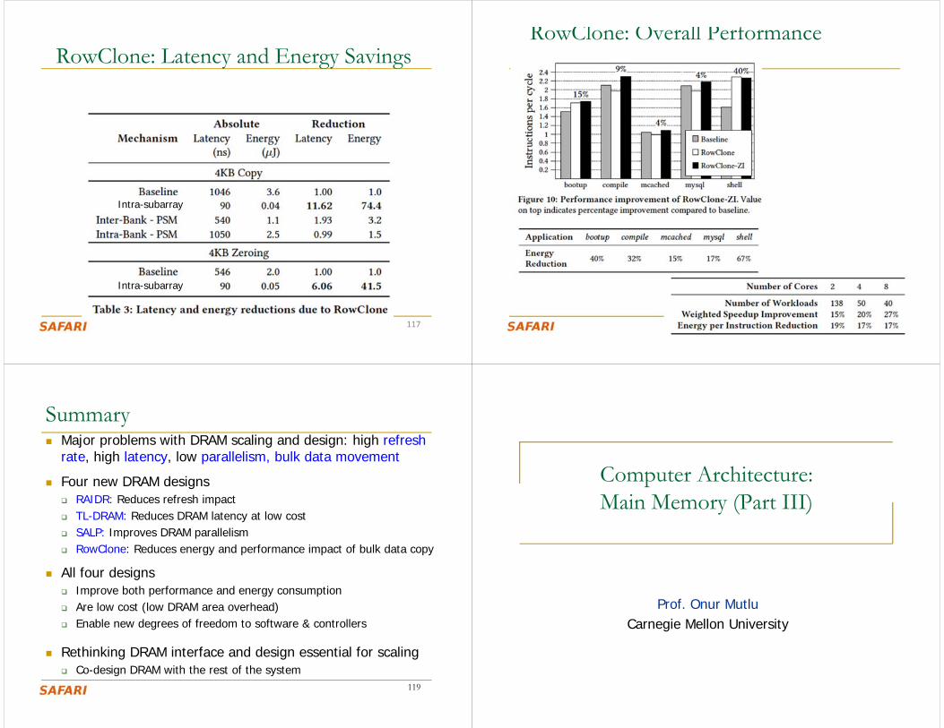
Summary Major problems with DRAM scaling and design: high refresh
rate, high latency, low parallelism, bulk data movement
Four new DRAM designs RAIDR: Reduces refresh impact TL-DRAM: Reduces DRAM latency at low cost SALP: Improves DRAM parallelism RowClone: Reduces energy and performance impact of bulk data copy
All four designs Improve both performance and energy consumption Are low cost (low DRAM area overhead) Enable new degrees of freedom to software & controllers
Rethinking DRAM interface and design essential for scaling Co-design DRAM with the rest of the system
119
Computer Architecture:Main Memory (Part III)
Prof. Onur MutluCarnegie Mellon University


![Twtr chamber112811 revised [compatibility mode]](https://img.dokumen.tips/doc/110x75/556317d7d8b42a51498b4fbb/twtr-chamber112811-revised-compatibility-mode-558499992ef8a.jpg)