Embed Size (px)
Citation preview
IEEE JOURNAL OF SOLID-STATE CIRCUITS, VOL. 47, NO. 5, MAY 2012 1075
Reliability Characterization and Modeling Solutionto Predict Aging of 40-nm MOSFET DC and RF
Performances Induced by RF StressesLaurent Negre, Student Member, IEEE, David Roy, Florian Cacho, Patrick Scheer, Sebastien Jan, Samuel Boret,
Daniel Gloria, and Gérard Ghibaudo, Senior Member, IEEE
Abstract—In the framework ofMOSFET reliability forRF/AMSapplications, a deep investigation of RF parameters degradation isperformed. An innovative flow, composed of DC and RF stresseswith DC and RF aging characterization, is presented. Degradationkinetics of main parameters are physically explained and modeledusing PSP compact model to predict the behavior of stressed de-vices.
Index Terms—Aging, compact model, hot carrier, load-pull,model, MOSFET, PSP, radio frequency, reliability.
I. INTRODUCTION
S INCE several years, radio frequency (RF) and analog-mixed-signal (AMS) CMOS technologies serve the
enormous momentum of the wireless market. The increasingdemand requires technologies meeting the highest standardsof performance and reliability. As depicted in Fig. 1, a bench-mark of RF CMOS cut-off frequency trends across technologygeneration shows that channel length downscaling enableaggressive performances. In contrast to these ever-increasingperformances, reliability is becoming a growing up concern.RF products are generally targeting mission profiles where
voltage swings are far beyond digital perimeter. As an examplePower Amplifiers are subjected to high input power and inthis way to voltage and current exceeding the nominal value.Today’s reliability models have been developed at device levelto be more predictive at product level. These reliability modelsare generally based on accelerated tests done under constantbias (DC) stress conditions and without experiments coveringthe real mission profile conditions.In this context new concerns will arise on the validity of the
models, the aging of key parameters, the interpretation of peakvalue over the whole signal. Thus, a key challenge is to extendcurrent reliability models allowing quantification and predic-tion of both DC and RF performances evolution under DC andRF/AMS stress conditions.
Manuscript received September 30, 2011; revised November 18, 2011; ac-cepted December 18, 2011. Date of publication February 17, 2012; date of cur-rent version April 25, 2012. This paper was approved by Guest Editor GeorgBoeck.L. Negre, D. Roy, F. Cacho, P. Scheer, S. Jan, S. Boret, and D. Gloria are with
STMicroelectronics, Technology Platform Sustaining/Electrical Characteriza-tion and Reliability, F-38926 Crolles, France (e-mail: [email protected]).G. Ghibaudo is with the IMEP-LAHC, 38016 Grenoble Cedex 1, France.Color versions of one or more of the figures in this paper are available online
at http://ieeexplore.ieee.org.Digital Object Identifier 10.1109/JSSC.2012.2185549
Fig. 1. Benchmark of NMOS cut-off frequency across technology gener-ation.
Over the last twenty years, several works have considered theextension of the reliability models in AC and RF/AMS cases.The study in [1] revealed a correlation between the RF figures ofMerits ( and ) degradation and DC performance degra-dation. An interesting suggestion of this work was to study thephysical degradation of the small signal model parameters inorder to predict the RF performance degradation from the DCperformance degradation.The study in [2] modeled RF performances degradation under
AC stress conditions. However, this study was limited to empir-ical adjustments of model parameters to represent the stresseddevice behavior.Regarding RF stress conditions [3]–[5], the studies were re-
stricted to the application of RF power considering only the fre-quency domain and in this way couldn’t use a quasi-static ap-proach based on DC reliability models.To effectively investigate the device aging in the AC/RF
range, a specific methodology will be developed and discussedin this paper. In Section II, a review of reliability phenomenaand associated DC model will be done. Then, the aging for-malism will be detailed in Section II-C to enable the extensionof the reliability models in the AC and RF range. In Section III,the complete experimental and analytical methodology for suchan extension will be presented. Based on this methodology,modeling of DC and RF performances under DC, AC and RFstress conditions will be performed on 40-nm technology nodein Section IV and V.
0018-9200/$31.00 © 2012 IEEE
1076 IEEE JOURNAL OF SOLID-STATE CIRCUITS, VOL. 47, NO. 5, MAY 2012
II. HOT CARRIERS RELIABILITY CONCERN
The front-end physical phenomena mostly responsible for thetransistor degradation are Hot Carrier (HC), Bias TemperatureInstability (BTI) and Time Dependent Dielectric Breakdown(TDDB). However, with the MOS channel length downscalingthe HC is becoming a first order concern for RF/AMS applica-tions.
A. Hot-Carrier Phenomenon
The HC phenomenon appears with the combination of gatevoltage and drain voltage applied to the transistor.The so-called hot carriers refer to carriers that gain high kineticenergy through regions of high electric field.Thus, under saturation conditions, the majority of the carriers
transit in the pinch-off region by ballistic transport and experi-ence no scattering events. Under the influence of the lateral fieldeffect, a fraction of those hot carriers interacts with the interfa-cial layer enabling a transfer of energy. Several mechanisms canexplain such interactions and are listed in [6]; an important oneis the impact ionization (II). A few carriers generated via impactionization are redirected and injected in the gate oxide. A directmeasurement of these carriers is done through the bulk currentwhich is proportional to the hole-electron pairs generated viaII. Carriers injected in the gate oxide can either contribute tothe gate leakage current or generate defects by Si-H bond dis-sociation in a region closed to the gate/oxide interfacial layer.Several types of bonds excitations can occur depending on theenergy (voltage) and the flow (current) of carriers. Recent work[7] highlights three main bonds excitations.• Single Vibrational Excitation (SVE) is related to higher en-ergetic carrier that has enough energy to break Si-H bond.
• Electron Electron Scattering (EES) is due to energy ex-change between two carriers. One carrier promotes theother into higher energy and allows Si-H breaking.
• Multiple Vibrational Excitation (MVE) is due to a seriesof low energetic carriers that accumulate enough energy tobreak Si-H bond.
In addition to the HC phenomenon described above, anotherimportant configuration has to be introduced i.e. the noncon-ducting HC [8]. This configuration appears when there’s nochannel . The high energy of the minority carriertransport also contributes to the degradation.
B. Hot-Carrier Physical Model
Under HC stress, the amount of degradation undergones tothe device follows a power law dependence of the stress timeand has been empirically verified in [6]
(1)
represents the degradation of a parameters e.g. linear orsaturated current, threshold voltage, maximum of transconduc-tance. The parameter depends on many parameters such asthe device architecture, the device geometry and the bias con-ditions. Based on the three excitations described before (SVE,
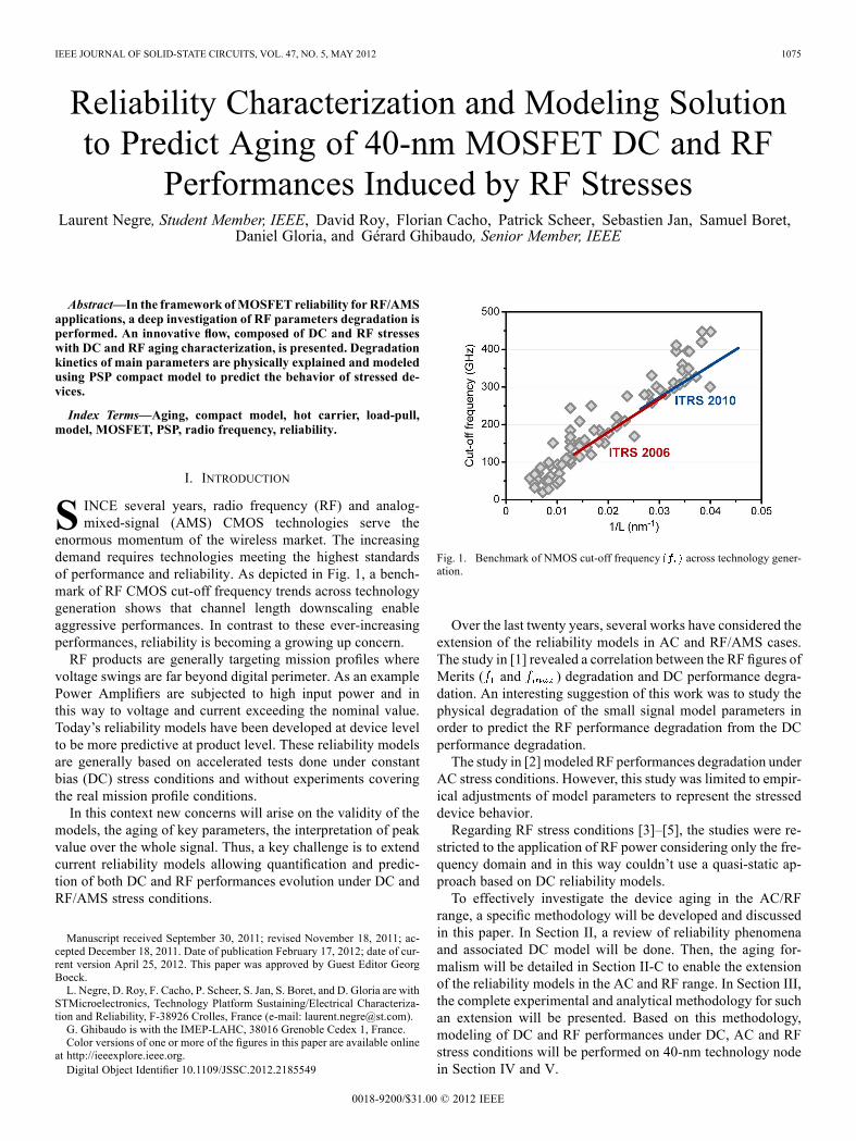
Fig. 2. Representation of the lifetime for the 40 nm technology, defined asthe time to reach a fixed saturated current drift, as function of and
revealing the three HC modes.
EES, MVE) a general expression of in the wholerange is given by [7], [9]
(2)
where , and are constant associated toeach excitation type. and respectively refer to the bulkand drain current. Physical descriptions of the other constantsare detailed in [7]. As shown in Fig. 2, this multimode HCmodel clearly consider the existence of three independentmodes. However, the nonconducting HC phenomenon is notaccounted for yet.
C. From Static (DC) to Radio Frequency (RF)
The HCmodel has historically been developed for DC condi-tions. However, in RF/AMS applications, the model should beable to take into account time-varying voltage and current pro-files. To account for these conditions, the HC model built fromDC conditions should be used through the quasi-static approxi-mation i.e. the possibility to assume the time-varying conditionsas a succession of DC conditions.Considering the threemodes HCmodel for a drift of the linear
drain current under time-varying conditions, (1) be-comes
(3)
NEGRE et al.: RELIABILITY CHARACTERIZATION AND MODELING SOLUTION 1077
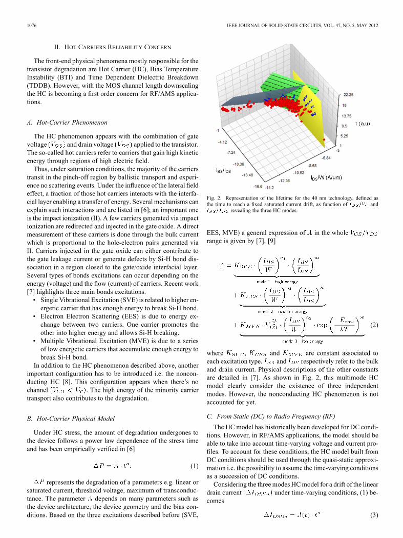
Fig. 3. Experimental setup used to perform DC and RF signal stresses. The stress can be interrupted periodically to characterize DC and RF parameters.
with
(4)
Equation (3) can be differentiated at both sides as done below
(5)
This differentiation allows the evaluation of the instantaneousrate of additional degradation as a function of the cumulateddegradation
(6)
This result can be rewritten to obtain
(7)
Since the time power law exponent used is valid for all stressconditions and provided that the quasi-static approximationholds, Equation (7) leads to the total degradation drift which isobtained thanks to the integration of the instantaneous degrada-tion rate linked to the corresponding instantaneous voltage as
(8)
This result introduces the so-called Age function already re-ported in the literature [10], [11]. This age formalism associ-ated to the three modes HC model clearly highlights that RFreliability needs to be performed by using time domain analysisrather than frequency domain analysis. Indeed, frequency do-main analysis is limited to power aspect, so that a major partof the information is lost and does not allow for a quantitative
analysis of the transistor’s aging. That’s why it will be manda-tory in this study to built and validate RF aging model usingtime varying voltage and current.However, it is important to note that this model is based on
quasi-static approximation. In this context, one can imaginethat a frequency discontinuity exists so that the non quasi-staticmodel would be no longer applicable for reliability study.Indeed, the RF stress could induced a non equilibrium leadingto a dissociation between the current’s flow and the carriersenergy. As described before, degradation mechanisms for DCcase are essentially based on a coupling of current and energy.In that case a discontinuity of the model could appear for higherfrequency. As mentioned in [12], this frequency limitation canbe evaluate through the pulsation
(9)
where is the mobility and the substrate factor.Thus, it is generally assumed that a frequency signal overintroduce non-quasistatic effects. The carrier’s delay time
become equal to the signal period and the MOS transistor is nomore governed by electrostatic equations.
III. RF RELIABILITY METHODOLOGY
A. Experimental Procedure
As presented in Fig. 3, a passive load pull setup is used inorder to perform DC or RF stress which is periodically inter-rupted for DC and RF measurements.Concerning the stress, the parametric analyzer and the syn-
thesizer are used to apply DC and RF stress component on theDevice Under Test (DUT) respectively. For the measurements,the parametric analyzer and the vector network analyzer (VNA)are used to monitor DC parameters and scattering (S) parame-ters from 1GHz to 50GHz respectively.The power meter is used to monitor the input power level de-
livered by the synthesizer and the impedance tuners are usedto control the impedances presented to the DUT. The spectrumanalyzer is used to monitor the output power level and also totake into account signal distortion induced by harmonics gener-ation. The use of switches allows to automatically calibrate thebench, extract and apply the RF signal, and also measure S-pa-rameters of the DUT. By this way, setup configurations betweendifferent calibration steps and measurements are highly repeat-able and the measurement accuracy is improved.
1078 IEEE JOURNAL OF SOLID-STATE CIRCUITS, VOL. 47, NO. 5, MAY 2012
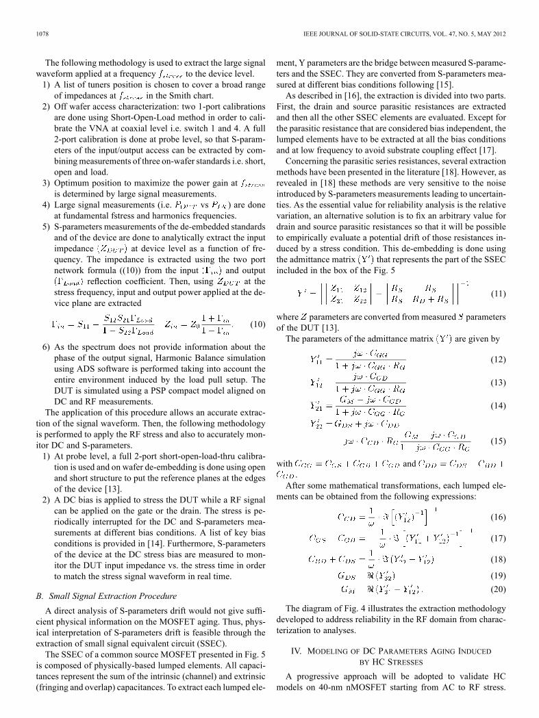
The following methodology is used to extract the large signalwaveform applied at a frequency to the device level.1) A list of tuners position is chosen to cover a broad rangeof impedances at in the Smith chart.
2) Off wafer access characterization: two 1-port calibrationsare done using Short-Open-Load method in order to cali-brate the VNA at coaxial level i.e. switch 1 and 4. A full2-port calibration is done at probe level, so that S-param-eters of the input/output access can be extracted by com-biningmeasurements of three on-wafer standards i.e. short,open and load.
3) Optimum position to maximize the power gain atis determined by large signal measurements.
4) Large signal measurements (i.e. vs ) are doneat fundamental fstress and harmonics frequencies.
5) S-parameters measurements of the de-embedded standardsand of the device are done to analytically extract the inputimpedance at device level as a function of fre-quency. The impedance is extracted using the two portnetwork formula ((10)) from the input and output
reflection coefficient. Then, using at thestress frequency, input and output power applied at the de-vice plane are extracted
(10)
6) As the spectrum does not provide information about thephase of the output signal, Harmonic Balance simulationusing ADS software is performed taking into account theentire environment induced by the load pull setup. TheDUT is simulated using a PSP compact model aligned onDC and RF measurements.
The application of this procedure allows an accurate extrac-tion of the signal waveform. Then, the following methodologyis performed to apply the RF stress and also to accurately mon-itor DC and S-parameters.1) At probe level, a full 2-port short-open-load-thru calibra-tion is used and on wafer de-embedding is done using openand short structure to put the reference planes at the edgesof the device [13].
2) A DC bias is applied to stress the DUT while a RF signalcan be applied on the gate or the drain. The stress is pe-riodically interrupted for the DC and S-parameters mea-surements at different bias conditions. A list of key biasconditions is provided in [14]. Furthermore, S-parametersof the device at the DC stress bias are measured to mon-itor the DUT input impedance vs. the stress time in orderto match the stress signal waveform in real time.
B. Small Signal Extraction Procedure
A direct analysis of S-parameters drift would not give suffi-cient physical information on the MOSFET aging. Thus, phys-ical interpretation of S-parameters drift is feasible through theextraction of small signal equivalent circuit (SSEC).The SSEC of a common source MOSFET presented in Fig. 5
is composed of physically-based lumped elements. All capaci-tances represent the sum of the intrinsic (channel) and extrinsic(fringing and overlap) capacitances. To extract each lumped ele-
ment, Y parameters are the bridge between measured S-parame-ters and the SSEC. They are converted from S-parameters mea-sured at different bias conditions following [15].As described in [16], the extraction is divided into two parts.
First, the drain and source parasitic resistances are extractedand then all the other SSEC elements are evaluated. Except forthe parasitic resistance that are considered bias independent, thelumped elements have to be extracted at all the bias conditionsand at low frequency to avoid substrate coupling effect [17].Concerning the parasitic series resistances, several extraction
methods have been presented in the literature [18]. However, asrevealed in [18] these methods are very sensitive to the noiseintroduced by S-parameters measurements leading to uncertain-ties. As the essential value for reliability analysis is the relativevariation, an alternative solution is to fix an arbitrary value fordrain and source parasitic resistances so that it will be possibleto empirically evaluate a potential drift of those resistances in-duced by a stress condition. This de-embedding is done usingthe admittance matrix that represents the part of the SSECincluded in the box of the Fig. 5
(11)
where parameters are converted from measured parametersof the DUT [13].The parameters of the admittance matrix are given by
(12)
(13)
(14)
(15)
with and.
After some mathematical transformations, each lumped ele-ments can be obtained from the following expressions:
(16)
(17)
(18)
(19)
(20)
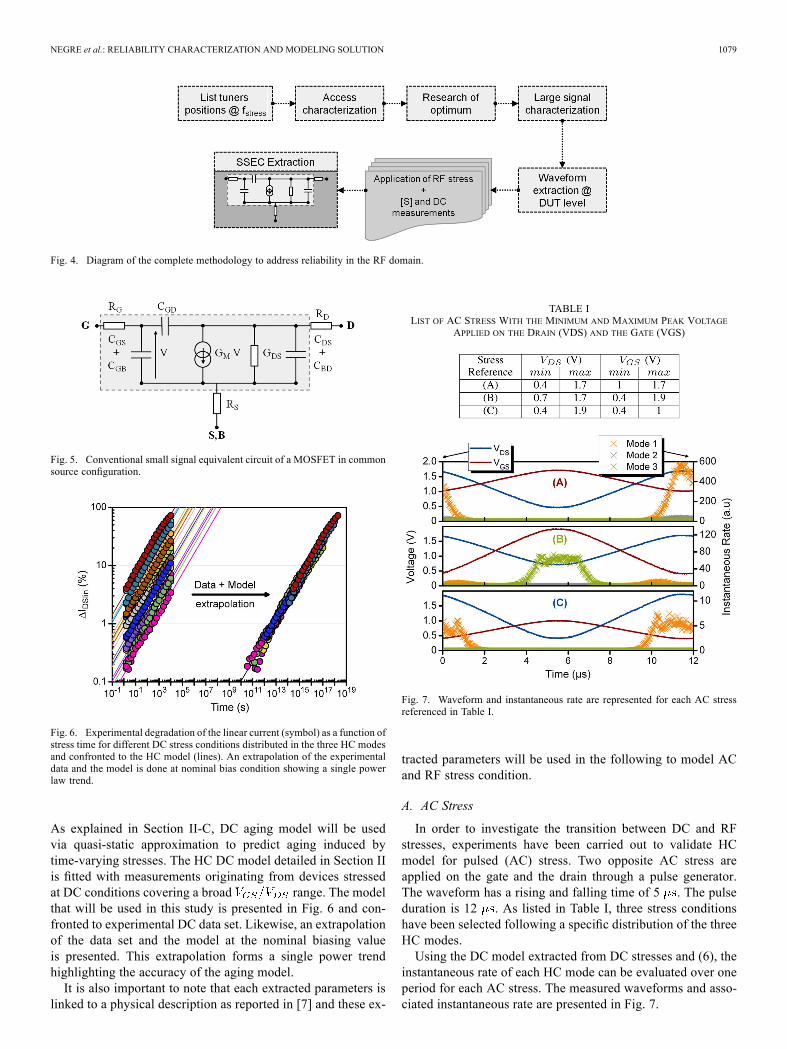
The diagram of Fig. 4 illustrates the extraction methodologydeveloped to address reliability in the RF domain from charac-terization to analyses.
IV. MODELING OF DC PARAMETERS AGING INDUCEDBY HC STRESSES
A progressive approach will be adopted to validate HCmodels on 40-nm nMOSFET starting from AC to RF stress.
NEGRE et al.: RELIABILITY CHARACTERIZATION AND MODELING SOLUTION 1079
Fig. 4. Diagram of the complete methodology to address reliability in the RF domain.
Fig. 5. Conventional small signal equivalent circuit of a MOSFET in commonsource configuration.
Fig. 6. Experimental degradation of the linear current (symbol) as a function ofstress time for different DC stress conditions distributed in the three HC modesand confronted to the HC model (lines). An extrapolation of the experimentaldata and the model is done at nominal bias condition showing a single powerlaw trend.
As explained in Section II-C, DC aging model will be usedvia quasi-static approximation to predict aging induced bytime-varying stresses. The HC DC model detailed in Section IIis fitted with measurements originating from devices stressedat DC conditions covering a broad range. The modelthat will be used in this study is presented in Fig. 6 and con-fronted to experimental DC data set. Likewise, an extrapolationof the data set and the model at the nominal biasing valueis presented. This extrapolation forms a single power trendhighlighting the accuracy of the aging model.It is also important to note that each extracted parameters is
linked to a physical description as reported in [7] and these ex-
TABLE ILIST OF AC STRESS WITH THE MINIMUM AND MAXIMUM PEAK VOLTAGE
APPLIED ON THE DRAIN (VDS) AND THE GATE (VGS)
Fig. 7. Waveform and instantaneous rate are represented for each AC stressreferenced in Table I.
tracted parameters will be used in the following to model ACand RF stress condition.
A. AC Stress
In order to investigate the transition between DC and RFstresses, experiments have been carried out to validate HCmodel for pulsed (AC) stress. Two opposite AC stress areapplied on the gate and the drain through a pulse generator.The waveform has a rising and falling time of 5 . The pulseduration is 12 . As listed in Table I, three stress conditionshave been selected following a specific distribution of the threeHC modes.Using the DC model extracted from DC stresses and (6), the
instantaneous rate of each HC mode can be evaluated over oneperiod for each AC stress. The measured waveforms and asso-ciated instantaneous rate are presented in Fig. 7.
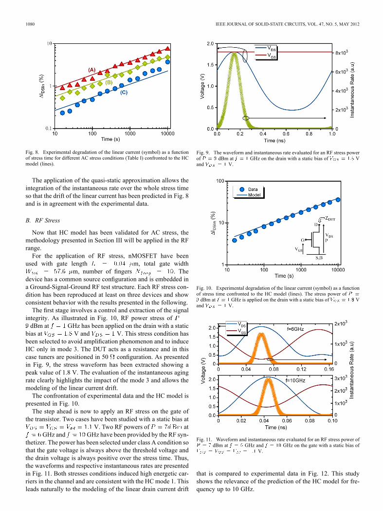
1080 IEEE JOURNAL OF SOLID-STATE CIRCUITS, VOL. 47, NO. 5, MAY 2012
Fig. 8. Experimental degradation of the linear current (symbol) as a functionof stress time for different AC stress conditions (Table I) confronted to the HCmodel (lines).
The application of the quasi-static approximation allows theintegration of the instantaneous rate over the whole stress timeso that the drift of the linear current has been predicted in Fig. 8and is in agreement with the experimental data.
B. RF Stress
Now that HC model has been validated for AC stress, themethodology presented in Section III will be applied in the RFrange.For the application of RF stress, nMOSFET have been
used with gate length m, total gate widthm, number of fingers . The
device has a common source configuration and is embedded ina Ground-Signal-Ground RF test structure. Each RF stress con-dition has been reproduced at least on three devices and showconsistent behavior with the results presented in the following.The first stage involves a control and extraction of the signal
integrity. As illustrated in Fig. 10, RF power stress ofdBm at GHz has been applied on the drain with a staticbias at V and V. This stress condition hasbeen selected to avoid amplification phenomenon and to induceHC only in mode 3. The DUT acts as a resistance and in thiscase tuners are positioned in 50 configuration. As presentedin Fig. 9, the stress waveform has been extracted showing apeak value of 1.8 V. The evaluation of the instantaneous agingrate clearly highlights the impact of the mode 3 and allows themodeling of the linear current drift.The confrontation of experimental data and the HC model is
presented in Fig. 10.The step ahead is now to apply an RF stress on the gate of
the transistor. Two cases have been studied with a static bias atV. Two RF powers of at
GHz and GHz have been provided by the RF syn-thetizer. The power has been selected under class A condition sothat the gate voltage is always above the threshold voltage andthe drain voltage is always positive over the stress time. Thus,the waveforms and respective instantaneous rates are presentedin Fig. 11. Both stresses conditions induced high energetic car-riers in the channel and are consistent with the HC mode 1. Thisleads naturally to the modeling of the linear drain current drift
Fig. 9. The waveform and instantaneous rate evaluated for an RF stress powerof dBm at GHz on the drain with a static bias of Vand V.
Fig. 10. Experimental degradation of the linear current (symbol) as a functionof stress time confronted to the HC model (lines). The stress power ofdBm at GHz is applied on the drain with a static bias of Vand V.
Fig. 11. Waveform and instantaneous rate evaluated for an RF stress power ofdBm at GHz and GHz on the gate with a static bias of
V.
that is compared to experimental data in Fig. 12. This studyshows the relevance of the prediction of the HC model for fre-quency up to 10 GHz.
NEGRE et al.: RELIABILITY CHARACTERIZATION AND MODELING SOLUTION 1081
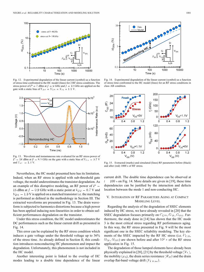
Fig. 12. Experimental degradation of the linear current (symbol) as a functionof stress time confronted to the HCmodel (lines) for 2 RF stress conditions. Thestress power of dBm at GHz and GHz are applied on thegate with a static bias of V.
Fig. 13. Waveform and instantaneous rate evaluated for an RF stress power ofdBm at GHz on the gate with a static bias of V
and V.
Nevertheless, the HC model presented here has its limitation.Indeed, when an RF stress is applied with sub-threshold gatevoltage, the model underestimates the transistor degradation. Asan example of this disruptive modeling, an RF power ofdBm at GHz with a static point at V and
V is applied on amatched transistor i.e. thematchingis performed as defined in the methodology in Section III. Theextracted waveforms are presented in Fig. 13. The drain wave-form is subjected to harmonics distortions because a high powerhas been applied inducing non-linearities in order to obtain suf-ficient performances degradation on the transistor.Under this stress condition, the HC model underestimates the
DC performances such as the linear current drift as presented inFig. 14.This error can be explained by the RF stress condition which
induces a gate voltage under the threshold voltage up to 36%of the stress time. As already defined in Section II, this condi-tion introduces nonconducting HC phenomenon and impact thedegradation. Unfortunately, this phenomenon is not included inthe HC model.Another interesting point is linked to the overlap of HC
modes leading to a double time dependence of the linear
Fig. 14. Experimental degradation of the linear current (symbol) as a functionof stress time confronted to the HC model (lines) for an RF stress conditions inclass AB condition.
Fig. 15. Extracted (marks) and simulated (lines) RF parameters before (black)and after (red) 1000 s of RF stress.
current drift. The double time dependence can be observed aton Fig. 14. More details are given in [19], these time
dependencies can be justified by the interaction and defectslocation between the mode 1 and non-conducting HC.
V. INTEGRATION OF RF PARAMETERS AGING AT COMPACTMODELING LEVEL
Regarding the analysis of the degradation of SSEC elementsinduced by HC stress, we have already revealed in [20] that theSSEC degradation focuses primarily on , , . Fur-thermore, the study done in [14] has shown that the HC mode3 is the most critical stress regarding RF performances aging.In this way, the RF stress presented in Fig. 9 will be the mostsignificant one in the SSEC reliability modeling. The key ele-ments of the SSEC impacted by the RF HC stress (i.e. ,
, ) are shown before and after of the RF stressapplication in Fig. 15.The degradation of those lumped elements have already been
physically explained in [20], [21] by the threshold voltage ,the mobility , the drain series resistance and the drainoverlap flat-band voltage drift .
1082 IEEE JOURNAL OF SOLID-STATE CIRCUITS, VOL. 47, NO. 5, MAY 2012
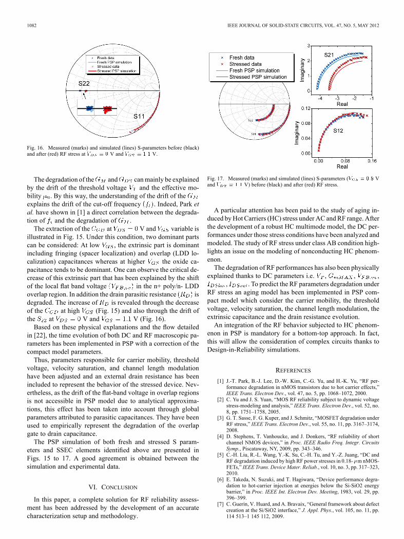
Fig. 16. Measured (marks) and simulated (lines) S-parameters before (black)and after (red) RF stress at V and V.
The degradation of the and canmainly be explainedby the drift of the threshold voltage and the effective mo-bility . By this way, the understanding of the drift of theexplains the drift of the cut-off frequency . Indeed, Park etal. have shown in [1] a direct correlation between the degrada-tion of and the degradation of .The extraction of the at V and variable is
illustrated in Fig. 15. Under this condition, two dominant partscan be considered: At low , the extrinsic part is dominantincluding fringing (spacer localization) and overlap (LDD lo-calization) capacitances whereas at higher the oxide ca-pacitance tends to be dominant. One can observe the critical de-crease of this extrinsic part that has been explained by the shiftof the local flat band voltage in the n+ poly/n- LDDoverlap region. In addition the drain parasitic resistance isdegraded. The increase of is revealed through the decreaseof the at high (Fig. 15) and also through the drift ofthe at V and V (Fig. 16).Based on these physical explanations and the flow detailed
in [22], the time evolution of both DC and RF macroscopic pa-rameters has been implemented in PSP with a correction of thecompact model parameters.Thus, parameters responsible for carrier mobility, threshold
voltage, velocity saturation, and channel length modulationhave been adjusted and an external drain resistance has beenincluded to represent the behavior of the stressed device. Nev-ertheless, as the drift of the flat-band voltage in overlap regionsis not accessible in PSP model due to analytical approxima-tions, this effect has been taken into account through globalparameters attributed to parasitic capacitances. They have beenused to empirically represent the degradation of the overlapgate to drain capacitance.The PSP simulation of both fresh and stressed S param-
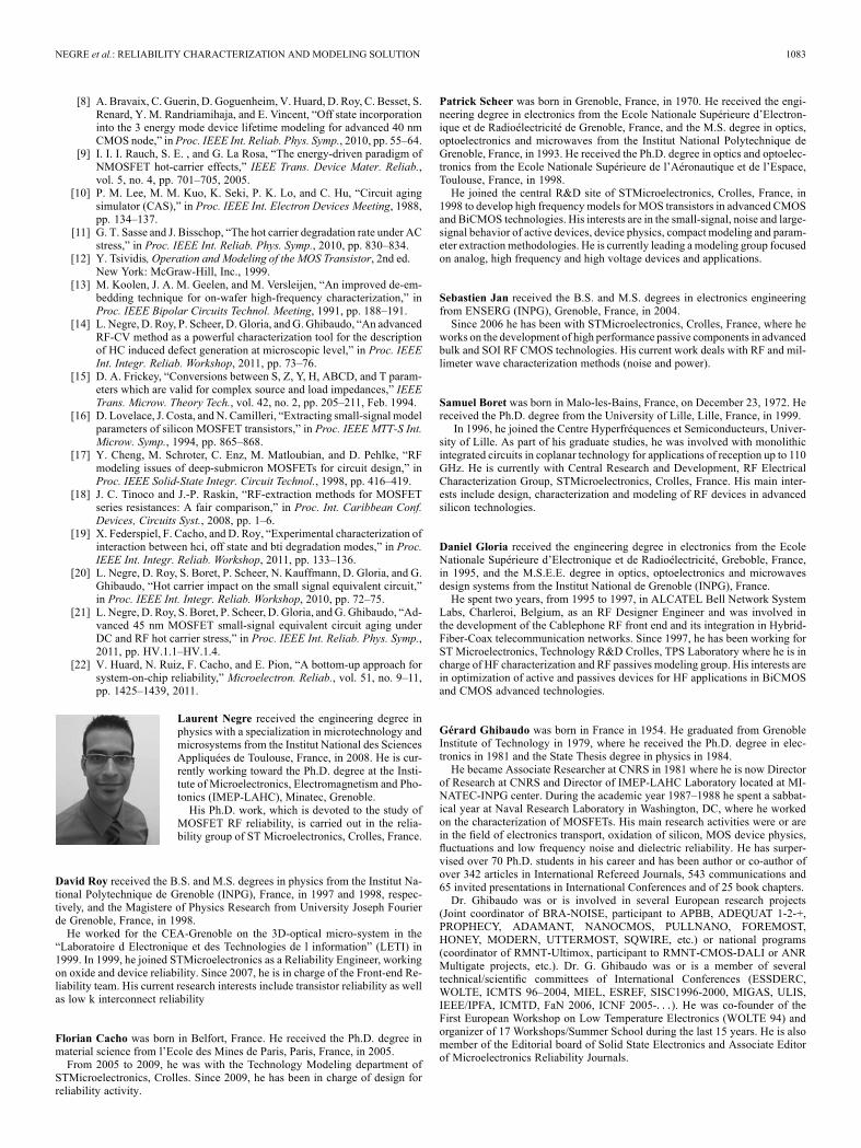
eters and SSEC elements identified above are presented inFigs. 15 to 17. A good agreement is obtained between thesimulation and experimental data.
VI. CONCLUSION
In this paper, a complete solution for RF reliability assess-ment has been addressed by the development of an accuratecharacterization setup and methodology.
Fig. 17. Measured (marks) and simulated (lines) S-parameters ( Vand V) before (black) and after (red) RF stress.
A particular attention has been paid to the study of aging in-duced byHot Carriers (HC) stress under AC and RF range. Afterthe development of a robust HC multimode model, the DC per-formances under those stress conditions have been analyzed andmodeled. The study of RF stress under class AB condition high-lights an issue on the modeling of nonconducting HC phenom-enon.The degradation of RF performances has also been physically
explained thanks to DC parameters i.e. , , ,, . To predict the RF parameters degradation under
RF stress an aging model has been implemented in PSP com-pact model which consider the carrier mobility, the thresholdvoltage, velocity saturation, the channel length modulation, theextrinsic capacitance and the drain resistance evolution.An integration of the RF behavior subjected to HC phenom-
enon in PSP is mandatory for a bottom-top approach. In fact,this will allow the consideration of complex circuits thanks toDesign-in-Reliability simulations.
REFERENCES
[1] J.-T. Park, B.-J. Lee, D.-W. Kim, C.-G. Yu, and H.-K. Yu, “RF per-formance degradation in nMOS transistors due to hot carrier effects,”IEEE Trans. Electron Dev., vol. 47, no. 5, pp. 1068–1072, 2000.
[2] C. Yu and J. S. Yuan, “MOS RF reliability subject to dynamic voltagestress-modeling and analysis,” IEEE Trans. Electron Dev., vol. 52, no.8, pp. 1751–1758, 2005.
[3] G. T. Sasse, F. G. Kuper, and J. Schmitz, “MOSFET degradation underRF stress,” IEEE Trans. Electron Dev., vol. 55, no. 11, pp. 3167–3174,2008.
[4] D. Stephens, T. Vanhoucke, and J. Donkers, “RF reliability of shortchannel NMOS devices,” in Proc. IEEE Radio Freq. Integr. CircuitsSymp., Piscataway, NY, 2009, pp. 343–346.
[5] C.-H. Liu, R.-L. Wang, Y.-K. Su, C.-H. Tu, and Y.-Z. Juang, “DC andRF degradation induced by high RF power stresses in 0.18- m nMOS-FETs,” IEEE Trans. Device Mater. Reliab., vol. 10, no. 3, pp. 317–323,2010.
[6] E. Takeda, N. Suzuki, and T. Hagiwara, “Device performance degra-dation to hot-carrier injection at energies below the Si-SiO2 energybarrier,” in Proc. IEEE Int. Electron Dev. Meeting, 1983, vol. 29, pp.396–399.
[7] C. Guerin, V. Huard, and A. Bravaix, “General framework about defectcreation at the Si/SiO2 interface,” J. Appl. Phys., vol. 105, no. 11, pp.114 513–1 145 112, 2009.
NEGRE et al.: RELIABILITY CHARACTERIZATION AND MODELING SOLUTION 1083
[8] A. Bravaix, C. Guerin, D. Goguenheim, V. Huard, D. Roy, C. Besset, S.Renard, Y. M. Randriamihaja, and E. Vincent, “Off state incorporationinto the 3 energy mode device lifetime modeling for advanced 40 nmCMOS node,” in Proc. IEEE Int. Reliab. Phys. Symp., 2010, pp. 55–64.
[9] I. I. I. Rauch, S. E. , and G. La Rosa, “The energy-driven paradigm ofNMOSFET hot-carrier effects,” IEEE Trans. Device Mater. Reliab.,vol. 5, no. 4, pp. 701–705, 2005.
[10] P. M. Lee, M. M. Kuo, K. Seki, P. K. Lo, and C. Hu, “Circuit agingsimulator (CAS),” in Proc. IEEE Int. Electron Devices Meeting, 1988,pp. 134–137.
[11] G. T. Sasse and J. Bisschop, “The hot carrier degradation rate under ACstress,” in Proc. IEEE Int. Reliab. Phys. Symp., 2010, pp. 830–834.
[12] Y. Tsividis, Operation and Modeling of the MOS Transistor, 2nd ed.New York: McGraw-Hill, Inc., 1999.
[13] M. Koolen, J. A. M. Geelen, and M. Versleijen, “An improved de-em-bedding technique for on-wafer high-frequency characterization,” inProc. IEEE Bipolar Circuits Technol. Meeting, 1991, pp. 188–191.
[14] L. Negre, D. Roy, P. Scheer, D. Gloria, andG. Ghibaudo, “An advancedRF-CV method as a powerful characterization tool for the descriptionof HC induced defect generation at microscopic level,” in Proc. IEEEInt. Integr. Reliab. Workshop, 2011, pp. 73–76.
[15] D. A. Frickey, “Conversions between S, Z, Y, H, ABCD, and T param-eters which are valid for complex source and load impedances,” IEEETrans. Microw. Theory Tech., vol. 42, no. 2, pp. 205–211, Feb. 1994.
[16] D. Lovelace, J. Costa, andN. Camilleri, “Extracting small-signal modelparameters of silicon MOSFET transistors,” in Proc. IEEE MTT-S Int.Microw. Symp., 1994, pp. 865–868.
[17] Y. Cheng, M. Schroter, C. Enz, M. Matloubian, and D. Pehlke, “RFmodeling issues of deep-submicron MOSFETs for circuit design,” inProc. IEEE Solid-State Integr. Circuit Technol., 1998, pp. 416–419.
[18] J. C. Tinoco and J.-P. Raskin, “RF-extraction methods for MOSFETseries resistances: A fair comparison,” in Proc. Int. Caribbean Conf.Devices, Circuits Syst., 2008, pp. 1–6.
[19] X. Federspiel, F. Cacho, and D. Roy, “Experimental characterization ofinteraction between hci, off state and bti degradation modes,” in Proc.IEEE Int. Integr. Reliab. Workshop, 2011, pp. 133–136.
[20] L. Negre, D. Roy, S. Boret, P. Scheer, N. Kauffmann, D. Gloria, and G.Ghibaudo, “Hot carrier impact on the small signal equivalent circuit,”in Proc. IEEE Int. Integr. Reliab. Workshop, 2010, pp. 72–75.
[21] L. Negre, D. Roy, S. Boret, P. Scheer, D. Gloria, andG. Ghibaudo, “Ad-vanced 45 nm MOSFET small-signal equivalent circuit aging underDC and RF hot carrier stress,” in Proc. IEEE Int. Reliab. Phys. Symp.,2011, pp. HV.1.1–HV.1.4.
[22] V. Huard, N. Ruiz, F. Cacho, and E. Pion, “A bottom-up approach forsystem-on-chip reliability,” Microelectron. Reliab., vol. 51, no. 9–11,pp. 1425–1439, 2011.
Laurent Negre received the engineering degree inphysics with a specialization in microtechnology andmicrosystems from the Institut National des SciencesAppliquées de Toulouse, France, in 2008. He is cur-rently working toward the Ph.D. degree at the Insti-tute of Microelectronics, Electromagnetism and Pho-tonics (IMEP-LAHC), Minatec, Grenoble.His Ph.D. work, which is devoted to the study of
MOSFET RF reliability, is carried out in the relia-bility group of ST Microelectronics, Crolles, France.
David Roy received the B.S. and M.S. degrees in physics from the Institut Na-tional Polytechnique de Grenoble (INPG), France, in 1997 and 1998, respec-tively, and the Magistere of Physics Research from University Joseph Fourierde Grenoble, France, in 1998.He worked for the CEA-Grenoble on the 3D-optical micro-system in the
“Laboratoire d Electronique et des Technologies de l information” (LETI) in1999. In 1999, he joined STMicroelectronics as a Reliability Engineer, workingon oxide and device reliability. Since 2007, he is in charge of the Front-end Re-liability team. His current research interests include transistor reliability as wellas low k interconnect reliability
Florian Cacho was born in Belfort, France. He received the Ph.D. degree inmaterial science from l’Ecole des Mines de Paris, Paris, France, in 2005.From 2005 to 2009, he was with the Technology Modeling department of
STMicroelectronics, Crolles. Since 2009, he has been in charge of design forreliability activity.
Patrick Scheer was born in Grenoble, France, in 1970. He received the engi-neering degree in electronics from the Ecole Nationale Supérieure d’Electron-ique et de Radioélectricité de Grenoble, France, and the M.S. degree in optics,optoelectronics and microwaves from the Institut National Polytechnique deGrenoble, France, in 1993. He received the Ph.D. degree in optics and optoelec-tronics from the Ecole Nationale Supérieure de l’Aéronautique et de l’Espace,Toulouse, France, in 1998.He joined the central R&D site of STMicroelectronics, Crolles, France, in
1998 to develop high frequency models forMOS transistors in advanced CMOSand BiCMOS technologies. His interests are in the small-signal, noise and large-signal behavior of active devices, device physics, compact modeling and param-eter extraction methodologies. He is currently leading amodeling group focusedon analog, high frequency and high voltage devices and applications.
Sebastien Jan received the B.S. and M.S. degrees in electronics engineeringfrom ENSERG (INPG), Grenoble, France, in 2004.Since 2006 he has been with STMicroelectronics, Crolles, France, where he
works on the development of high performance passive components in advancedbulk and SOI RF CMOS technologies. His current work deals with RF and mil-limeter wave characterization methods (noise and power).
Samuel Boret was born in Malo-les-Bains, France, on December 23, 1972. Hereceived the Ph.D. degree from the University of Lille, Lille, France, in 1999.In 1996, he joined the Centre Hyperfréquences et Semiconducteurs, Univer-
sity of Lille. As part of his graduate studies, he was involved with monolithicintegrated circuits in coplanar technology for applications of reception up to 110GHz. He is currently with Central Research and Development, RF ElectricalCharacterization Group, STMicroelectronics, Crolles, France. His main inter-ests include design, characterization and modeling of RF devices in advancedsilicon technologies.
Daniel Gloria received the engineering degree in electronics from the EcoleNationale Supérieure d’Electronique et de Radioélectricité, Greboble, France,in 1995, and the M.S.E.E. degree in optics, optoelectronics and microwavesdesign systems from the Institut National de Grenoble (INPG), France.He spent two years, from 1995 to 1997, in ALCATEL Bell Network System
Labs, Charleroi, Belgium, as an RF Designer Engineer and was involved inthe development of the Cablephone RF front end and its integration in Hybrid-Fiber-Coax telecommunication networks. Since 1997, he has been working forST Microelectronics, Technology R&D Crolles, TPS Laboratory where he is incharge of HF characterization and RF passives modeling group. His interests arein optimization of active and passives devices for HF applications in BiCMOSand CMOS advanced technologies.
Gérard Ghibaudo was born in France in 1954. He graduated from GrenobleInstitute of Technology in 1979, where he received the Ph.D. degree in elec-tronics in 1981 and the State Thesis degree in physics in 1984.He became Associate Researcher at CNRS in 1981 where he is now Director
of Research at CNRS and Director of IMEP-LAHC Laboratory located at MI-NATEC-INPG center. During the academic year 1987–1988 he spent a sabbat-ical year at Naval Research Laboratory in Washington, DC, where he workedon the characterization of MOSFETs. His main research activities were or arein the field of electronics transport, oxidation of silicon, MOS device physics,fluctuations and low frequency noise and dielectric reliability. He has surper-vised over 70 Ph.D. students in his career and has been author or co-author ofover 342 articles in International Refereed Journals, 543 communications and65 invited presentations in International Conferences and of 25 book chapters.Dr. Ghibaudo was or is involved in several European research projects
(Joint coordinator of BRA-NOISE, participant to APBB, ADEQUAT 1-2-+,PROPHECY, ADAMANT, NANOCMOS, PULLNANO, FOREMOST,HONEY, MODERN, UTTERMOST, SQWIRE, etc.) or national programs(coordinator of RMNT-Ultimox, participant to RMNT-CMOS-DALI or ANRMultigate projects, etc.). Dr. G. Ghibaudo was or is a member of severaltechnical/scientific committees of International Conferences (ESSDERC,WOLTE, ICMTS 96–2004, MIEL, ESREF, SISC1996-2000, MIGAS, ULIS,IEEE/IPFA, ICMTD, FaN 2006, ICNF 2005- ). He was co-founder of theFirst European Workshop on Low Temperature Electronics (WOLTE 94) andorganizer of 17 Workshops/Summer School during the last 15 years. He is alsomember of the Editorial board of Solid State Electronics and Associate Editorof Microelectronics Reliability Journals.