Embed Size (px)
Citation preview

1
Digital Design and Synthesis
INTRODUCTION
The advances in digital design owe its progress to 3 factors. First the acceleration at which the
CMOS technology has advanced in last few decades and the way that information has been
stored and processed. Secondly, the driver for digital design has been the ability to treat all kinds
of media as digital data that is stored, processed and manipulated and finally combining and
storing all sorts of information and data in a single document and the third parameter is, the
transmission in high speed over long distances. These concepts increased the requirement for
digital design and ways to optimise its performance.
StructuralBehavioural
Physical
Algorithmic
Micro architecture
Logic
Circuit
Rectangles
Cells
Macro-cells
Modules
Chips, boards…
Processor
Hardware modules
ALU, registers
Gates, F/Fs
Transistors
Systems
Algorithms
Register transfer
Logic
Transfer function
Fig.1 Design description levels

2
Digital system and its design can be described in three domains namely: Behavioural,
Structural and Physical domains as shown in Fig.1. In each domain, the level of description
and decision to be taken and the complexity are different.
The behavioural description is usually language based and can be pure algorithmic or signal flow
graphs or even a transfer function and more likely a HDL Code. For example a multiplier can be
described by A * B = C. At the behavioural level we may decide in using a serial or a parallel
multiplier. So trade offs for speed, cost, chip area, power consumption etc. is made in this level.
Many high level details are decided upon while the lower level details are compromised.
Important design decisions such as what algorithm to be used for the system at hand are made at
this level. It is important to know that the reward for optimization at this level is many folds of
that of other levels as shown in Fig. 2. The digital designer starts the design at the conceptual
level working with high level behavioural blocks and proceeds to design of major functional
blocks that supports a given design specification. In order to manage complexity, the overall
design may be partitioned and each partition dealt with separately using detailed structural
constructs. In any case major decisions regarding algorithms, functional partitioning, structural
partitioning and data transmission methods are made at this level while for each individual item
optimising the speed, power consumption, area, and cost are identified. The benefit to the
designer is that it provides a fast and accurate way to verify whether the concept is correct and
design specification can be met and also provides means by which a compromise is reached
between several objectives by “WHAT IF ANALYSIS”.
The behavioural analysis is used usually for “PROOF OF CONCEPT”.

3
Level Transformation Expected Power Saving
Algorithmic Algorithm selection Orders of magnitude
Behavioural Concurrency Several times
Register Transfer Level Structural transformations ~10 - 15%
Clock control ~10 - 90%
Data/signal encoding ~20%
Technology independent Extraction/decomposition ~15%
Technology dependant Technology mapping ~20%
Gate sizing ~20%
Layout Placement 20%
Optimization Levels
Fig-2
The behavioural model is usually converted to RTL level in HDL or block diagram usually
manually. At the structural level, we are dealing with data paths, practical logic blocks and their
interconnection. We may want to decide upon Dynamic logic or Static logic, Serial or Parallel
input registers, what kind of adder to be used, what kind of multiplier will meet our speed and
area, what is our clocking strategy etc. Our project for this course this year will based on
Structural level, where you would design and code a multiplier in VHDL at structural level and
then synthesise it to an FPGA. At the Structural level we use the EDA tools fully. At this level,
The synthesis tools convert the blocks to gate level netlist and the logic synthesis tools optimize
logic level design and the timing tools verify operations in terms of spec. requirement of timing,
area and power.
At the physical level, we will try to design and implement the circuit on chip. (COEN 6511)
where our variables will be at silicon level. At this level the netlist is input to the EDA tools
such as place and route which produces a layout, The layout is extracted and fed again for
verification through an iterative process. Once a final satisfaction with the spec is acheived the
layout is ready for download for fabrication. For example, how the chip layout is arranged,
where the pads will be located, and how the Vdd and Vss are distributed and how the boards are
arranged, where are the components placed etc.

4
The Y chart of Fig. 1 shows that one can make a de-composition and a transition from
behavioural level to structural level. This can be achieved manually or through silicon
compilation. By the same token one can transform from structural level to gate and logic level
by creating FFs, gates, and higher blocks such as registers, counters, all kinds of modules. Also
one can transcend to the physical level to design the transistors that make up the gates and step
further to the polygons of different materials that make the transistors. So one can start
automatically or manually to transcend from behavioural to the physical level. Silicon compilers
do exist that accept behavioural level description and proceed to the physical chip, or chip
layout. In all cases HDL language ie VHDL/ Verilog or others high languages is a good starting
point to describe the system at hand.
Generalizing then, logical synthesis is a structural form where the physical synthesis leads to the
physical domain. Thus the design process includes the behavioural description followed by the
decomposition of high level constructs into more precise functional units which are then mapped
into the physical elements. The logical circuits that are commonly used are available as
integrated circuits and are referred to as standard chips (in our design they are referred to as
library cells). The advent of the very large scale integration (VLSI) has made the configuration
on chip possible where a complete system can be designed synthesized and placed on a single
chip.
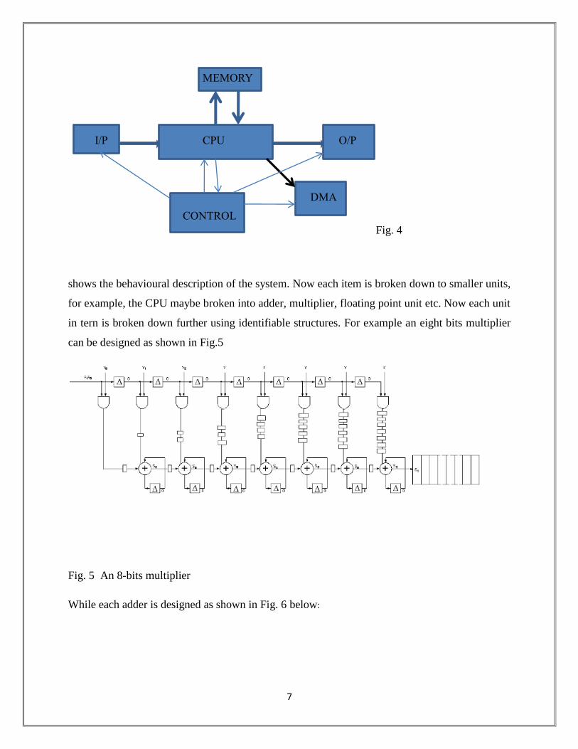
As complexity of the chips is increased to billions of transistors on a chip, then design
automation becomes necessary. Designers now can design large chips verify it, automatically
place and route it, re-evaluate its characteristic, debug it and verify its final functions before
downloading the bitmap file on the actual chip as Shown in Fig. 4. One must always that these
tools depend on the input and the rule of garbage in garbage out still applies.
In general nowadays HDL is used extensively in digital design. The advantages are many
including the design at the HDL level does not depend on any fabrication technology. Synthesis
tools are available for converting the HDL to gate level netlist. The HDL is adaptable to new
technologies, eliminating need for redesign. The verification tools at any step insure that all
bugs are cleared and the design once goes to production is correct producing the exact
requirement first time. Finally HDL, VHDL/Verilog/or higher level languages are becoming the

5
only method being used by designers. Currently the trend is to use structural design at the RTL
level.
In general two basic types of methodologies can be defined namely top-down design and bottom-
up design methodology. In top-down design methodology the top block is defined and then the
sub-blocks necessary are identified in order to build a top level block. These are then further
divided in progression into smaller units till we reach the leaf cells that cannot be divided further.
The design is described in HDL and the HDL coding techniques will be applied to the design so
that the design is modelled effectively and efficiently. Design errors that are obvious are checked
through the preliminary synthesis of each HDL code and every block is verified before
integrating it into a larger unit.
Design process
A design starts always with a specification. The specification describes what the circuit must do,
but not how it is done. The specification is usually set by the customer who wants the final
product. Once the designer knows what the circuit must do, she/he can begin to determine how
it is done, for example, defining what are the inputs to the unit and the outputs that must be
generated is a good first step.
The designer then starts with translating the design specification into behavioural description,
then decomposing the high level constructs into functional units and finally, then mapping these
units into physical elements as shown in Fig.3.

6
Fig. 3
A simple example of word specification from a customer may be as follows:
Required an 8 bit microprocessor, no cache, simple addressing mode, 8 internal registers,
Instruction word 8 bits, 8 bit address bus multiplexed with data bus, 40 pin package, dual IP
package and consuming less than 1 Watt. A simple diagram of the system is shown in Fig.4
The designer then gets to work as first step starting with block diagram, decomposes the overall
system into components that are available in the library or to be designed. The block diagram
below
Design Process:
It starts with behavioural
description, decomposing
the high level of constructs
into more precise functional
units, then mapping these
units into physical elements.
System Specification
Architectural Design
(behavioural)
Analysis
Design Implementation
(structural)
Analysis
Design Implementation
(Physical)
Analysis
7
Fig. 4
shows the behavioural description of the system. Now each item is broken down to smaller units,
for example, the CPU maybe broken into adder, multiplier, floating point unit etc. Now each unit
in tern is broken down further using identifiable structures. For example an eight bits multiplier
can be designed as shown in Fig.5
Fig. 5 An 8-bits multiplier
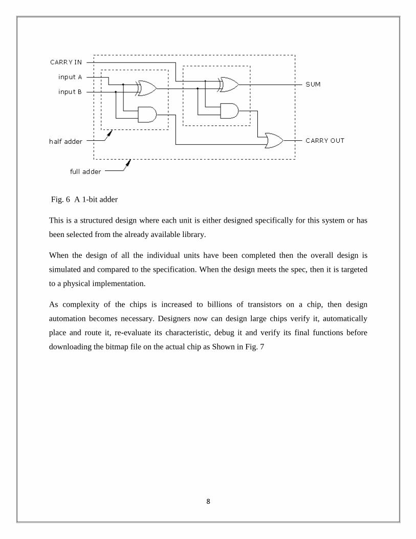
While each adder is designed as shown in Fig. 6 below:
CPU
CONTROL
MEMORY
DMA
O/P I/P
8
Fig. 6 A 1-bit adder
This is a structured design where each unit is either designed specifically for this system or has
been selected from the already available library.
When the design of all the individual units have been completed then the overall design is
simulated and compared to the specification. When the design meets the spec, then it is targeted
to a physical implementation.
As complexity of the chips is increased to billions of transistors on a chip, then design
automation becomes necessary. Designers now can design large chips verify it, automatically
place and route it, re-evaluate its characteristic, debug it and verify its final functions before
downloading the bitmap file on the actual chip as Shown in Fig. 7

9
Fig. 7
Design Strategies
Any system is comprised of many individual units such as boards, chips, power supply, routing
etc. The success of the overall system depends on how well it is optimized in terms of
performance, and at the end of the product cycle, what is the revenue that the newly designed
system generates. This in turn depends on how well each individual unit in the system was
designed through all its design levels from the algorithm down to the devices. For example how
well a chip is designed is measured by several criteria such as functionality, speed, power, size
etc. On the other hand other factors also play an important part such as time to design, time to
market and ease of testing. The final implementation has to conform to the original spec. or
better. During the design there are many factors that can be traded for the good design, therefore
the knowledge of all factors affecting the design and their interdependence are important.
Description
Behavioral
Verification Logic Synthesis/
Gate-Level Netlist
Verification Floor Planning/
Place & Route
Verification/
Final Timing
Implementation
specification
Proof of Concept
HDL Description
10
Most designs nowadays are large and complex. A successful designer has to structure his design
and use design automation tools available. In general a successful designer uses the following 4
principals to achieve his design effectively and quickly.
1) Hierarchy
2) Regularity
3) Modularity
4) Locality
Hierarchy,
This is an extremely useful strategy when you have a complex system. It is the process of divide
and conquer. The overall system is repeatedly divided into subunits and in turn the subunits are
divided further until no further division is possible or the subunits are available in the library. At
this stage the design is more manageable since the smaller sub-modules can be designed easier.
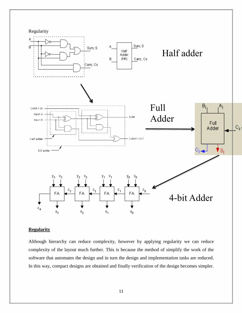
The hierarchy can be in different domains in software or hardware modules. For example a
VHDL entity module can be written or structurally designed in a hierarchical fashion. Parallel
hierarchy is implemented in all domains. As an example a 4-bit adder can be designed by
dividing the adder into 4 single bit adder, and an adder cab be designed using 2 half adders and
so on as shown below:
11
Regularity
Regularity
Although hierarchy can reduce complexity, however by applying regularity we can reduce
complexity of the layout much further. This is because the method of simplify the work of the
software that automates the design and in turn the design and implementation tasks are reduced.
In this way, compact designs are obtained and finally verification of the design becomes simpler.
Half adder
Full
Adder
4-bit Adder

12
So at this stage we divide the hierarchy into smaller building blocks such that the small block can
interlock in each other.
For example an adder in a datapath design can be designed in a regular fashion in such a way
that by concatenating the 1 bit of the adder n time an n bit adder is designed and implemented in
layout directly.
Modularity,
a
b
S
C
Vdd Cin Vss
Vdd Co Vss
Unit 1-bit Adder
Vdd Cin Vss
Vdd Cin Vss
ao
bo so
co
a7
b7
s7
c7
S0-S7
C7
ao-a7
bo-b7
Vdd Cin Vss
Vdd Co Vss
13
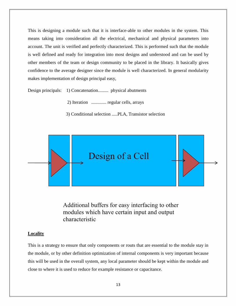
This is designing a module such that it is interface-able to other modules in the system. This
means taking into consideration all the electrical, mechanical and physical parameters into
account. The unit is verified and perfectly characterized. This is performed such that the module
is well defined and ready for integration into most designs and understood and can be used by
other members of the team or design community to be placed in the library. It basically gives
confidence to the average designer since the module is well characterized. In general modularity
makes implementation of design principal easy,
Design principals: 1) Concatenation......... physical abutments
2) Iteration ............. regular cells, arrays
3) Conditional selection .....PLA, Transistor selection
Locality
This is a strategy to ensure that only components or routs that are essential to the module stay in
the module, or by other definition optimization of internal components is very important because
this will be used in the overall system, any local parameter should be kept within the module and
close to where it is used to reduce for example resistance or capacitance.
Design of a Cell
Additional buffers for easy interfacing to other
modules which have certain input and output
characteristic
14
VHDL,
Due to complexity and speed of the design, designers have opted for design at higher level of
abstraction. Designers follow functionality and let the Electronic Design Automation EDA, take
care of the rest. The EDA tools are complete packages that take care of A to Z of the design
translation, optimization and implementation.
Most designs nowadays are performed with the aid of high evel languages such as VHDL or
Verilog. This is so because these languages are design entry point, Specification language, as
well as design simulation design verification tools. Thus it is a complete package by which the
designer starts the specification to the end point by which the final VHDL code can be translated
and synthesized into an FPGA or semi custom design. The design once described can be
simulated and iterated through the design cycle until the final specification targeting a device for
implementation is met. The following figure shows that most of the design, specification,
simulation and verification can be done through VHDL.

15
4
Implementation is vendor
dependent
Design
Specification
Modeling the behavior
English Prose
Data Path
Transfer Function,
Boolean Equations,
Flow Graphs, Pseudo
Codes
Logic Design
Computational
Units,Registers,
Buses
Flip Flops, Gates,
Netlist
Transistors, Wires
Masks
Manufacturing
V
H
D
L
Netlist, ASCII text describing gates or library
modules and their interconnection
ASIC FPGA
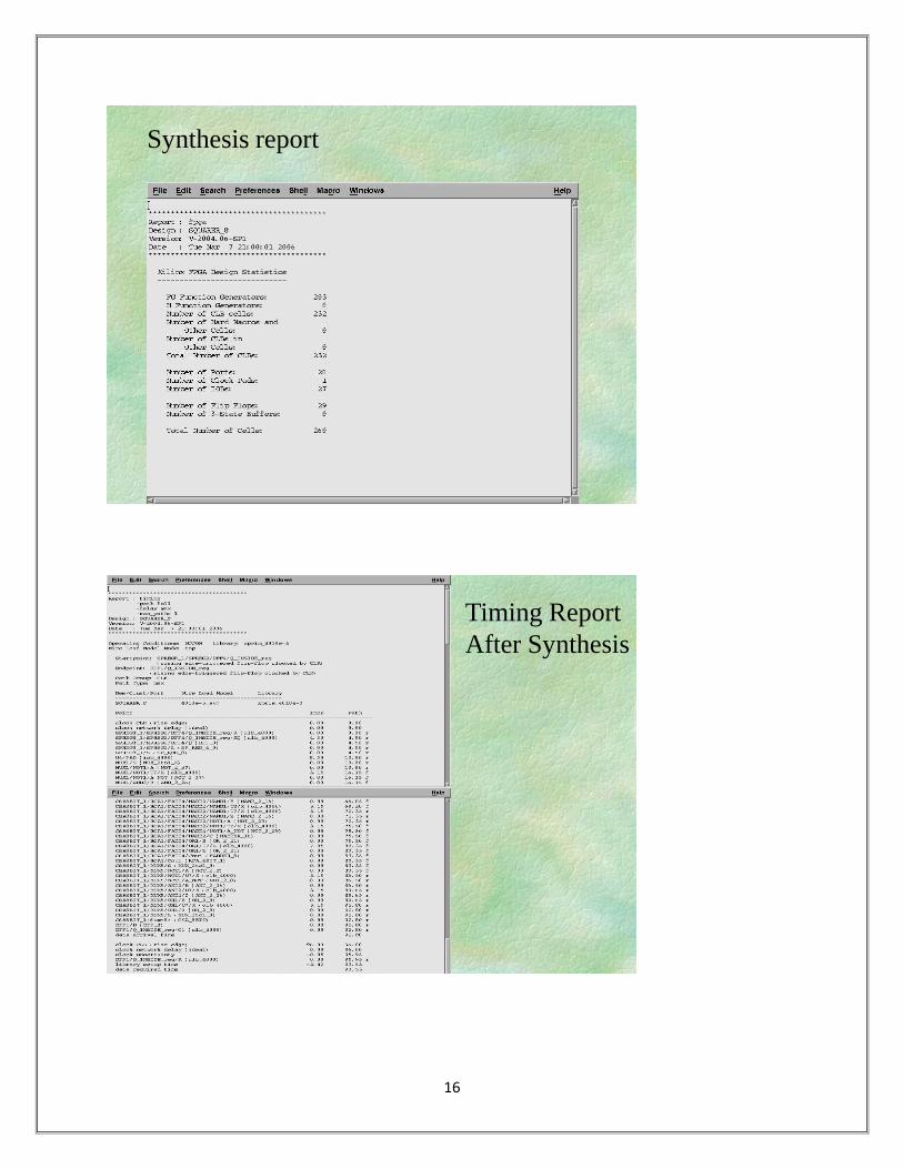
At each point the Synthesis tools will provide you a report to check the design and its
performance in terms of Speed, Area and Power. At anytime also the designer can go back and
change its design thus repeating the design process. The following diagrams show the output
from the synthesis reports.
At the end of this course you will be doing your project. That requires design of a digital system,
coding its behaviour at the structural level, writing the test bench, simulating the design and
verifying its functionality as well as obtaining its performance.
16
Synthesis report
Timing Report
After Synthesis

17
Area report after Synthesis
Power report after Synthesis
18
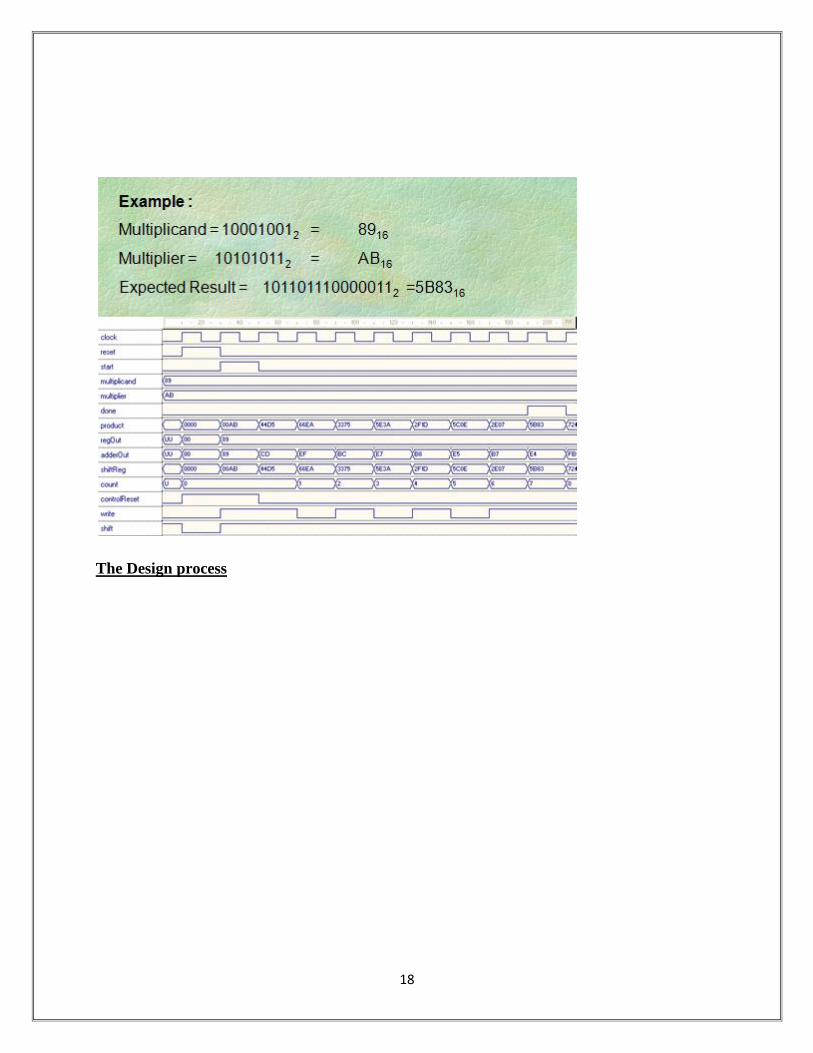
The Design process

19
Appendix A
20
By: Harish Harish prepared for COEN 6501
The following Appendix, shows the design concept using VHDL in details.
VHDL DESIGN CONCEPT
The behaviour and structure of the digital circuits are described by Hardware description
language which is also used to simulate the circuit and check its response. VHDL language
which is a simulation and verification language is basically used as a modelling language for
digital systems for many tools it is used as an intermediate form of design entry. VHDL is not
case sensitive and should be saved with an extension of “.vhd”. In a VHDL language the basic
building blocks is known as module which describes the corresponding hardware module. A
basic module structure may include declarations, statements, tasks and functions among others.
VHDL uses the ASCII character set. The lexical elements for the language include identifier and
reserve words special symbols etc.
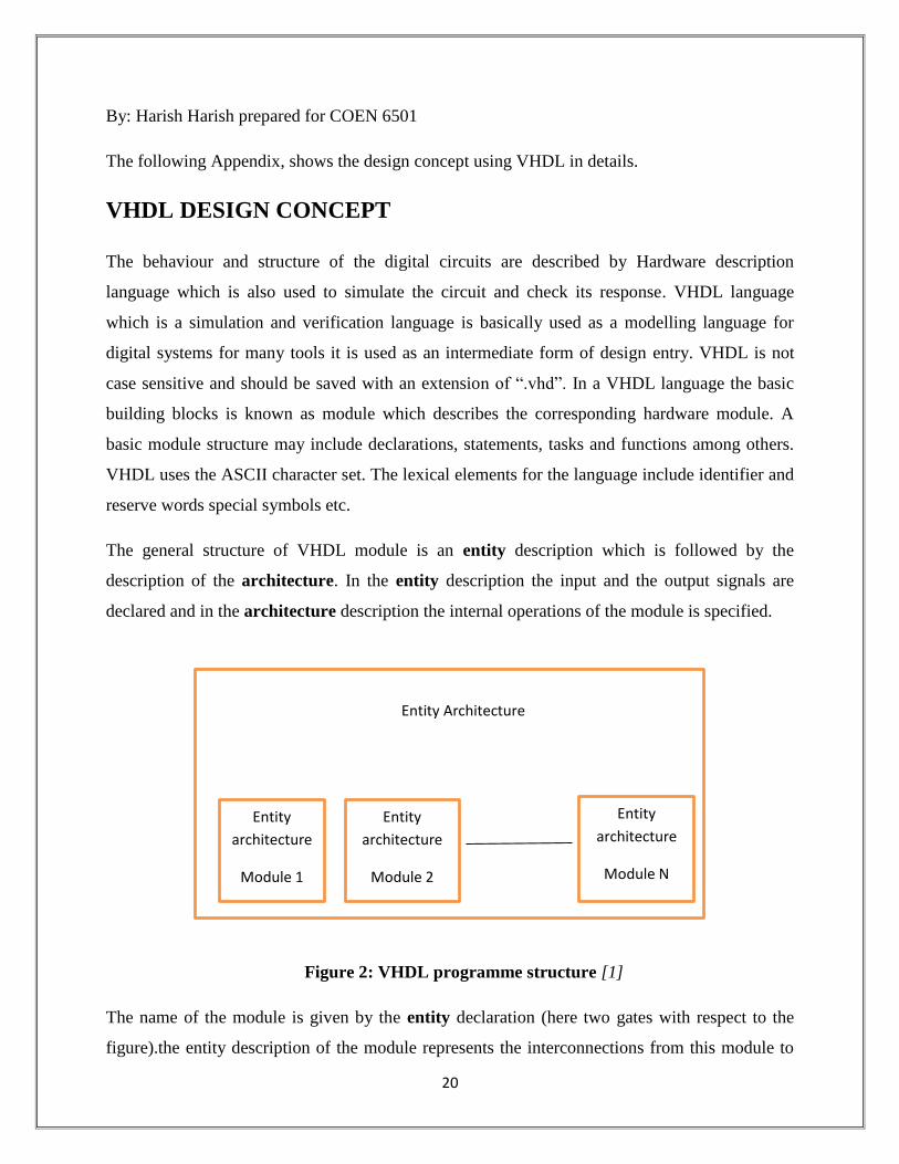
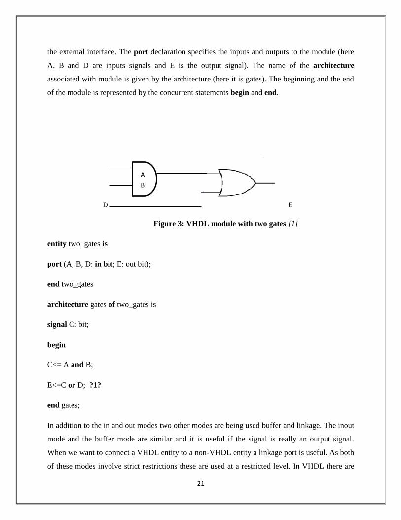
The general structure of VHDL module is an entity description which is followed by the
description of the architecture. In the entity description the input and the output signals are
declared and in the architecture description the internal operations of the module is specified.
Figure 2: VHDL programme structure [1]
The name of the module is given by the entity declaration (here two gates with respect to the
figure).the entity description of the module represents the interconnections from this module to
Entity Architecture
Entity
architecture
Module 1
Entity
architecture
Module 2
Entity
architecture
Module N
21
the external interface. The port declaration specifies the inputs and outputs to the module (here
A, B and D are inputs signals and E is the output signal). The name of the architecture
associated with module is given by the architecture (here it is gates). The beginning and the end
of the module is represented by the concurrent statements begin and end.
D E
Figure 3: VHDL module with two gates [1]
entity two_gates is
port (A, B, D: in bit; E: out bit);
end two_gates
architecture gates of two_gates is
signal C: bit;
begin
C<= A and B;
E<=C or D; ?1?
end gates;
In addition to the in and out modes two other modes are being used buffer and linkage. The inout
mode and the buffer mode are similar and it is useful if the signal is really an output signal.
When we want to connect a VHDL entity to a non-VHDL entity a linkage port is useful. As both
of these modes involve strict restrictions these are used at a restricted level. In VHDL there are
A
B

22
two types of delays which can be found-transport delays and inertial delays. Inertial delay
which is default delay is intended to model gats and to those devices which do not propagate
short pulses from input to output. The other VHDL delay which is the transport delay is intended
to model the delay introduced by the wiring, in other words it simply delays an input signal by a
specified delay time. Modelling this delay can be done by simply using the keyword transport
in the code. This simulation related delays like inertial delay can inhibit many output change.
Compilation and simulation of VHDL code
In order to verify the implement the intended design
correctly and also to verify if the design meets the specification simulation of the VHDL code is
necessary. Accordingly there are three phases in the simulation of the VHDL code: compilation,
elaboration and simulation.
Simulator commands
Intermediate simulation
Code data structure
Simulator output
Figure 4: Compilation and Simulation of VHDL code [1]
The syntax of the typed VHDL source code is verified to check if it adheres to the syntax and the
semantic rules by the compiler also called as the analyser. On a positive result the compiler
generates an intermediate code used by the simulator. In the elaboration process the VHDL
intermediate code is converted to a form used by the simulator. The simulator process consists
Compiler
Resource
library
Elaborator Simulator
Working library
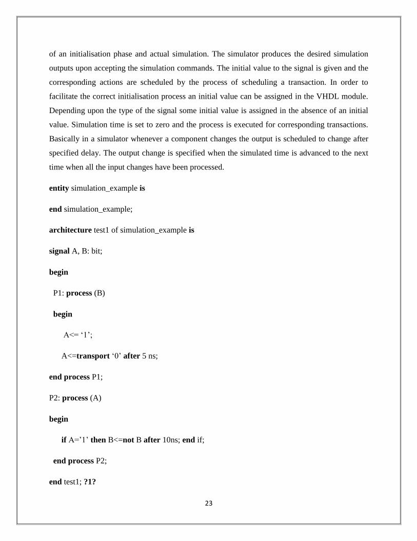
23
of an initialisation phase and actual simulation. The simulator produces the desired simulation
outputs upon accepting the simulation commands. The initial value to the signal is given and the
corresponding actions are scheduled by the process of scheduling a transaction. In order to
facilitate the correct initialisation process an initial value can be assigned in the VHDL module.
Depending upon the type of the signal some initial value is assigned in the absence of an initial
value. Simulation time is set to zero and the process is executed for corresponding transactions.
Basically in a simulator whenever a component changes the output is scheduled to change after
specified delay. The output change is specified when the simulated time is advanced to the next
time when all the input changes have been processed.
entity simulation_example is
end simulation_example;
architecture test1 of simulation_example is
signal A, B: bit;
begin
P1: process (B)
begin
A<= ‘1’;
A<=transport ‘0’ after 5 ns;
end process P1;
P2: process (A)
begin
if A=’1’ then B<=not B after 10ns; end if;
end process P2;
end test1; ?1?

24
VHDL data types and operators
In VHDL there are several predefined data types
which are used by the signals or they can also be user defined data type. Some of the data types
are bit (0 or 1), Boolean (FALSE or TRUE), integer (in the range of – (231-1) to + (231-1)), real
(floating point number), character (any legal VHDL character), time (any integer with the units if
fs, ps, ns, us, ms, sec, min, or hr). A common example of the user defined data type that is the
data type created by the user is the enumeration type. In VHDL signals and variables cannot be
mixed in the same assignment statement. Predefined VHDL operators are available and are
grouped into seven classes- Binary logical operators, relational operators, shift operators, adding
operators, unary operators, multiplying operators, miscellaneous operators. The operators in class
seven gets the highest precedence when the parenthesis are not used and are applied first which
is then followed by class six and then class five and so on. When operators of the same class are
used they get precedence from left to right and the order of the precedence can be changed by the
application of parenthesis. In the following expression
(A & not B or C ror 2 and D) = 110010
In the above relative expression, the operators are applied in the order
Not, &, ror, or, and, =
Lexical description
The VHDL text file is consisted of one or more text design files which must be prepared only
from the prescribed ASCII character set.
Character set
There are various character set which are allowed in the design file. Furthermore there lot of
characters which are included in the ASCII code representation to express like hexadecimal.
Lexical elements

25
A sequence of characters that makes up a fundamental element which cannot be divided into
smaller elements is called as lexical elements. The types of lexical elements: delimiter, identifier,
comment, character literal, string literal, bit string literal, abstract literal. The separators are those
which are used in between first lexical elements and after the last lexical elements. Many
separators can be used in between the lexical elements.
Delimiters
The character that is used in order to separate the lexical elements is called as delimiter. All
statements in VHDL are terminated using a “; “character. The sequence of two delimiters is
referred to as compound delimiter- =>, **,:=, /=, >=, <>, --. The use of delimiters reduces the
use of specific separators in between the lexical characters.
Character literal
When a lexical element is formed by inserting one character between two apostrophe delimiter, it
is known as character literal.
String literal
The lexical element formed by the insertion of sequence of graphical characters between two
quotation delimiters is called a string literal. Since it is a lexical element the string literal is typed
in one line. The number of characters in the sequence gives the length of the string literal.
Bit string literal
A lexical element which consists of a string of digits enclosed by the quotation character
delimiters and preceded by base specifier is called as bit string literal. The base specifier is one
of the letters like B-binary, O-octal, X-hexadecimal. The string of bits gives the value of a bit
string literal. The association of this to a numerical value is dependent on the user.
Decimal literal
26
An abstract literal which is used in many high level computer languages, expressed in standard
decimal notation is called as a decimal literal. The exponential part of the literal is proceeded by
letter E and only real literal accept the negative exponents value.
Data types
The specifications of values the object might have and the limitation of the types of operation the
object of that type needs to perform is indicated by the data type. It is named set of values. A
subtype is a type along with a constraint. If it is a legitimate value for the type and if the
constraint is satisfied, the value belongs to the subtype. The type from which it was constructed
is called the base type of the subtype. There are two classifications- scalar and composite.
SCALAR DATA TYPES
In scalar data types, the data types have single, simple values. An integer data type may have
value of 15. This includes enumeration data types, numeric data types and physical data types.
Enumeration types
An enumeration type is a scalar type in which the values are defined by simply ordering them in
a list. The elements may be identifiers or character literals. The two values for type bit are 0 and
1. Built in type for Boolean includes values TRUE or FALSE and for logical operators it is not,
or, and and xor. A pre-defined attribute is the one which the value function in the range is
associated with. The user-defined attribute is the one in which the attribute value is defined by
the user. Its general form is “attribute ATTRIBUTE_NAME:ATTRIBUTE_SUBTYPE;”
Numeric data types
Built-in numeric data types Integer and Real with its associated performance of addition,
subtraction, multiplication and division are present in VHDL language. The example for pre-
defined numeric data-types
Type Integer is range ---------;
Type Real is range ------------; ?2?
27
The ranges of the real and integer data types are implementation dependent which is in the range
of -2147483647 to +2147483647. The user-defined data types are constrained numeric data types
as the declaration constraints the range. The examples of user defined data types-
Type COUNTER is range 0 to 100 ?2?
Physical data types
A scalar numeric data type which is associated to a system of units and is used to represent
entities subject to physical measurements such as time, length, voltage, current is called as
physical data type. The only pre-defined data type is time which is represented as
Type TIME is range --------------;
The ranges of physical data types are restricted by implementations. The declaration of any
physical data type is allowed by an implementation which is in the range of -2147483647 to
+2147483647. When the range is within these limits any user-defined data type may have three
units as multiples of the next lower unit. Examples—
Type RESISTANCE is range 0 to Integer’ high
Type POWER is range 0 to le19 ?2?
COMPOSITE DATA TYPES
The composite data types have complex values and have several components associated with it
and it also represents an array of values with some relationship to one another.
Arrays
The data type in which each element has the same subtype i.e. homogeneous elements is called
as an array. There are generally two predefined array types namely string and Bit_Vector. The
former is used to define a character of elements and the latter is used to define an array of bits.
They are-
Type string is array (positive range <>) of character;
Type Bit_Vector is array (natural range <>) of bit; ?2?
28
Here the notation <> means the range is unconstrained, which indicates the user must specify the
range when declaring the object. Both string and Bit_Vector are unconstrained and the user has
to specify a range n positive for sting and in natural numbers for Bit_Vector. Some of the user
defined array data types
Type REGISTER_32_Bit is array (31 downto 0) of Bit;
Subtype BITVECT3 is Bit_Vector (0 to 2);
The REGISTER_32_Bit is a constrained array type which is descending in value. As the Bit
vector is an unconstrained data type, subtypes with specific index ranges can be declared.
BITVECT3 is a subtype of type Bit_Vector with an ascending index range 0 to 2.
Declaration of data objects
Before the referencing of the data types in assignment statement they must be declared. These
declared objects are subsequently used in the further section for various other statements.
Declaration of constants
In declaration of the constants it is imperial that their values are specified. The constant name is
separated from the type name by : delimiter and the type name is separated from a constant value
by := delimiter. Some examples are-
Constant ALPHA_LEVEL : PROBABILITY := 0.75;
Constant INITIAL_STATE : STATE := S0;
Constant END_MARKER : Character := DEL; ?2?
Declaration of variables
In declaration of variable it must be seen that they are declared within a process or sub
programme. The data type of the variable is specified by the variable declaration. In the
declaration the values of the variables are specified if not the default value which is the left
element in the type range specified in the declaration. Some examples are —
Variable STAR_COLOR, HAT_COLOR : COLOR;

29
Variable BETA_LEVEL : PROBABILITY := 0.0;
Variable A, B, C, D : Bit;
Variable R1, R2, R3, R4 : REG; ?2?
A , delimiter is used to in order to declare more than one variable of the same type. A : is used to
separate the list of variable name from the data type and := is used to separate the initial value
from the data type.
Declaration of signals
The signal declaration is similar to variable declaration. The signals are not be declared in
processes or in sub programmes but it can be declared as ports in entity declaration or in the
declarative region of architecture declarations. Some examples are ---
Signal X1, X2, X3, X4, X5: Bit;
Signal SR1, SR2, SR3, SR4: REG;
Signal DOWN_COUNT: COUNTER := COUNTER ‘right; ?2?
VHDL libraries
The functionality of the VHDL is extended by the
use of VHDL libraries and packages in defining types, functions, components and overloaded
operators. Overloaded functions are generally created to handle operations involving
heterogeneous data types. The package IEEE.std_logic_1164 defines a standard logic type which
has nine values likewise std_logic_vectors defines logic vectors. Both the packages define
overloaded arithmetic and logic operators for signed and unsigned numbers.
VHDL IMPLEMENTATION
Multiple forms of abstraction are possible. The same circuit can be implemented in different
ways namely Structural model, Behavioral model and Mixed model. In the behavioral VHDL

30
description, the circuit or the system is defined at a high level of abstraction without implying
any structure or technology specifying only the overall behaviour. The behavioral VHDL can
also be implemented as dataflow or algorithmic level. In the data flow model data flow and
control signals are specified. System working is specified in terms of data transfer between
registers.
DATA FLOW IMPLEMENTATION OF FULL ADDER
architecture DATA_FLOW_IMPLEMENTATION of FULL_ADDER is
block
signal S1, S2, S3: BIT;
begin
S1 <= A xor B;
SUM <= S1 xor CIN;
S2 <= A and B;
S3 <= S1 and CIN;
COUT <= S2 or S3;
end block;
end DATA_FLOW_IMPLEMENTATION; ?3?
ALGORITHMIC IMPLEMENTATION OF FULL ADDER
architecture ALGORITHMIC_IMPLEMENTATION of FULL_ADDER is
block
begin

31
process (A,B,CIN)
variable S: BIT_VECTOR ( 1 to 3 ) := A & B & CIN;
variable COUNT: INTEGER range 0 to 3 :=0;
begin
for i:= 1 to 3 loop
if S(i) = ‘1’ then
COUNT := COUNT +1;
end if ;
end loop;
case COUNT is
when 0 => COUT <= ‘0’; SUM <= ‘0’;
when 1 => COUT <= ‘0’; SUM <= ‘1’;
when 2 => COUT <= ‘1’; SUM <= ‘0’;
when 3 => COUT <= ‘1’; SUM <= ‘1’;
end case;
end process;
end block;
end ALGORITHIC-IMPLEMENTATION; ?3?
On the other hand in the implementation of the structural model which has a low level of
abstraction the components used and the interconnection between the components are clearly
specified. The structural model implementations are detailed enough to specify the use of
particular gates and flip-flops from specific libraries/packages.

32
STRUCTURAL IMPLEMENTATION OF FULL ADDER
architecture GATE_IMPLEMENTATION of FULL_ADDER is
Block
component or_gate port (A,B : in BIT; C: out BIT);
end component;
component and_gate port (A,B : in BIT; C: out BIT);
end component;
component xor_gate port (A,B : in BIT; C: out BIT);
end component;
signal S1, S2, S3: BIT;
begin
X1: xor_gate port map (A, B, S1);
X2: xor_gate port map (S1, CIN, SUM);
A1: and_gate port map (CIN, S1, S2);
A2: and_2 port map (A, B, S3);
O1: or_gate port map (S2, S3, COUT);
end Block;
end GATE_IMPLEMENTATION ; ?3?
Behavioral and structural design techniques are often combined giving rise to mixed VHDL
implementation. Here different techniques are used to design different parts of the module. The
automation tools generate efficient hardware hence they designed using behavioral level. Manual

33
optimisation needed by the memory structures are done through structural design as opposed to
the behavioral modelling.
MIXED IMPLEMENTATION OF FULL ADDER
architecture MIXED_IMPLEMENTATION of FULL_ADDER is
signal WIRE: BIT;
component XOR_G
port ( X1, X2: in BIT; XO1: out BIT);
end component;
for all: XOR_G use XOR_GATE(BEHAVIORAL);
begin
XOR1: XOR_G port map (X,Y,WIRE);
XOR2: XOR_G port map (WIRE,CIN,SUM);
COUT <= (WIRE and CIN) or (X and Y);
end MIXED_IMPLEMENTATION ?3?
SEQUENTIAL CIRCUITS AND VHDL IMPLEMENTATION
A combinational circuit is the one which produces its output based on the current inputs while a
sequential circuit generates the outputs based on the current inputs and the previous states, which
imply that memory, latches and flip-flops are common sequential circuits. The sequential logic
responds to changes dependent on the clock. The primitives are required to model selective
activity conditional on clock, edge triggered devices, sequences of operation in the process of
modelling sequential circuits.
34
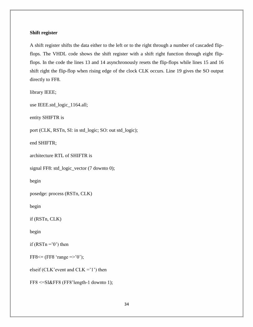
Shift register
A shift register shifts the data either to the left or to the right through a number of cascaded flip-
flops. The VHDL code shows the shift register with a shift right function through eight flip-
flops. In the code the lines 13 and 14 asynchronously resets the flip-flops while lines 15 and 16
shift right the flip-flop when rising edge of the clock CLK occurs. Line 19 gives the SO output
directly to FF8.
library IEEE;
use IEEE.std_logic_1164.all;
entity SHIFTR is
port (CLK, RSTn, SI: in std_logic; SO: out std_logic);
end SHIFTR;
architecture RTL of SHIFTR is
signal FF8: std_logic_vector (7 downto 0);
begin
posedge: process (RSTn, CLK)
begin
if (RSTn, CLK)
begin
if (RSTn =’0’) then
FF8<= (FF8 ‘range =>’0’);
elseif (CLK’event and CLK =’1’) then
FF8 <=SI&FF8 (FF8’length-1 downto 1);

35
end if;
end process;
SO <=FF8 (0);
end RTL; ?4?
SI SO
Figure 5: Synthesised schematic for shifter [2]
COMBINATIONAL CIRCUITS AND VHDL IMPLEMENTATION
The combinational circuits can be modelled by the VHDL by the use of concurrent statements.
These concurrent statements are those which are ready to be executed and which get evaluated
any time and also every time when the signal on the right side of the statement changes. VHDL
assignment statements can be given as an example for concurrent statements. The right side of
the concurrent statement is monitored by the VHDL simulator and when the signal changes the
right side expression is immediately re-evaluated. After an appropriate delay the new value is
assigned to the left side of the signal. The location of this concurrent statement in the programme
is not important.
Encoder
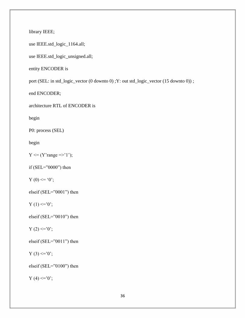
An encoder converts one form of input pattern to a required form of output pattern. Here the
encoder has a 4-bit input SEL and a 16-bit output Y. All the bits in the output will be 1, except
the value represented by SEL. In the first VHDL code the programme uses if statement inside the
process statement with the input SEL as process sensitivity list.
FD2
FD2
FD2
FD2
FD2
FD2
FD2
FD2
36
library IEEE;
use IEEE.std_logic_1164.all;
use IEEE.std_logic_unsigned.all;
entity ENCODER is
port (SEL: in std_logic_vector (0 downto 0) ;Y: out std_logic_vector (15 downto 0)) ;
end ENCODER;
architecture RTL of ENCODER is
begin
P0: process (SEL)
begin
Y <= (Y’range =>’1’);
if (SEL=”0000”) then
Y (0) <= ‘0’;
elseif (SEL=”0001”) then
Y (1) <=’0’;
elseif (SEL=”0010”) then
Y (2) <=’0’;
elseif (SEL=”0011”) then
Y (3) <=’0’;
elseif (SEL=”0100”) then
Y (4) <=’0’;

37
elseif (SEL=”0101”) then
Y (5) <=’0’;
elseif (SEL=”0110”) then
Y (6) <=’0’;
elseif (SEL=”0111”) then
Y (7) <=’0’;
elseif (SEL=”1000”) then
Y (8) <=’0’;
elseif (SEL=”1001”) then
Y (9) <=’0’;
elseif (SEL=”1010”) then
Y (10) <=’0’;
elseif (SEL=”1011”) then
Y (11) <=’0’;
elseif (SEL=”1100”) then
Y (12) <=’0’;
elseif (SEL=”1101”) then
Y (13) <=’0’;
elseif (SEL=”1110”) then
Y (14) <=’0’;
else

38
Y (51) <=’0’;
end if;
end process;
end RTL;
This coding uses a process statement and it includes conv_integer from the package IEEE
std_logic_unsigned.
architecture RTL of ENCODER is
begin
P3: process (SEL)
begin
Y <= (Y’range => ‘1’);
Y (conv_integer (SEL)) <= ‘0’;
end process;
end RTL; ?4?
PROGRAMMABLE LOGIC DEVICES
Programmable logic devices helps in the removal of multiple off-the shelf devices and the
inconvenience associated external wires. These devices allow an easy reprogramming and it is
easier to change the design in case of error. They basically contain an array of basic building
blocks that can be used to implement whatever functionality one desires. They differ in the
building blocks or the amount of programmability they provide.
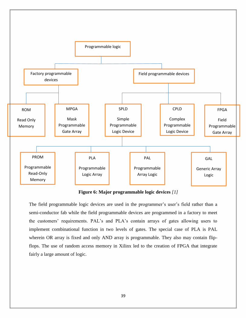
39
Figure 6: Major programmable logic devices [1]
The field programmable logic devices are used in the programmer’s user’s field rather than a
semi-conductor fab while the field programmable devices are programmed in a factory to meet
the customers’ requirements. PAL’s and PLA’s contain arrays of gates allowing users to
implement combinational function in two levels of gates. The special case of PLA is PAL
wherein OR array is fixed and only AND array is programmable. They also may contain flip-
flops. The use of random access memory in Xilinx led to the creation of FPGA that integrate
fairly a large amount of logic.
Programmable logic
Factory programmable
devices
Field programmable devices
ROM
Read Only
Memory
MPGA
Mask
Programmable
Gate Array
CPLD
Complex
Programmable
Logic Device
FPGA
Field
Programmable
Gate Array
SPLD
Simple
Programmable
Logic Device
PROM
Programmable
Read-Only
Memory
PLA
Programmable
Logic Array
PAL
Programmable
Array Logic
GAL
Generic Array
Logic
40
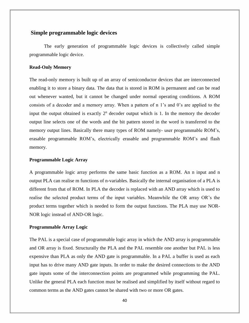
Simple programmable logic devices
The early generation of programmable logic devices is collectively called simple
programmable logic device.
Read-Only Memory
The read-only memory is built up of an array of semiconductor devices that are interconnected
enabling it to store a binary data. The data that is stored in ROM is permanent and can be read
out whenever wanted, but it cannot be changed under normal operating conditions. A ROM
consists of a decoder and a memory array. When a pattern of n 1’s and 0’s are applied to the
input the output obtained is exactly 2n decoder output which is 1. In the memory the decoder
output line selects one of the words and the bit pattern stored in the word is transferred to the
memory output lines. Basically there many types of ROM namely- user programmable ROM’s,
erasable programmable ROM’s, electrically erasable and programmable ROM’s and flash
memory.
Programmable Logic Array
A programmable logic array performs the same basic function as a ROM. An n input and n
output PLA can realise m functions of n-variables. Basically the internal organisation of a PLA is
different from that of ROM. In PLA the decoder is replaced with an AND array which is used to
realise the selected product terms of the input variables. Meanwhile the OR array OR’s the
product terms together which is needed to form the output functions. The PLA may use NOR-
NOR logic instead of AND-OR logic.
Programmable Array Logic
The PAL is a special case of programmable logic array in which the AND array is programmable
and OR array is fixed. Structurally the PLA and the PAL resemble one another but PAL is less
expensive than PLA as only the AND gate is programmable. In a PAL a buffer is used as each
input has to drive many AND gate inputs. In order to make the desired connections to the AND
gate inputs some of the interconnection points are programmed while programming the PAL.
Unlike the general PLA each function must be realised and simplified by itself without regard to
common terms as the AND gates cannot be shared with two or more OR gates.
41
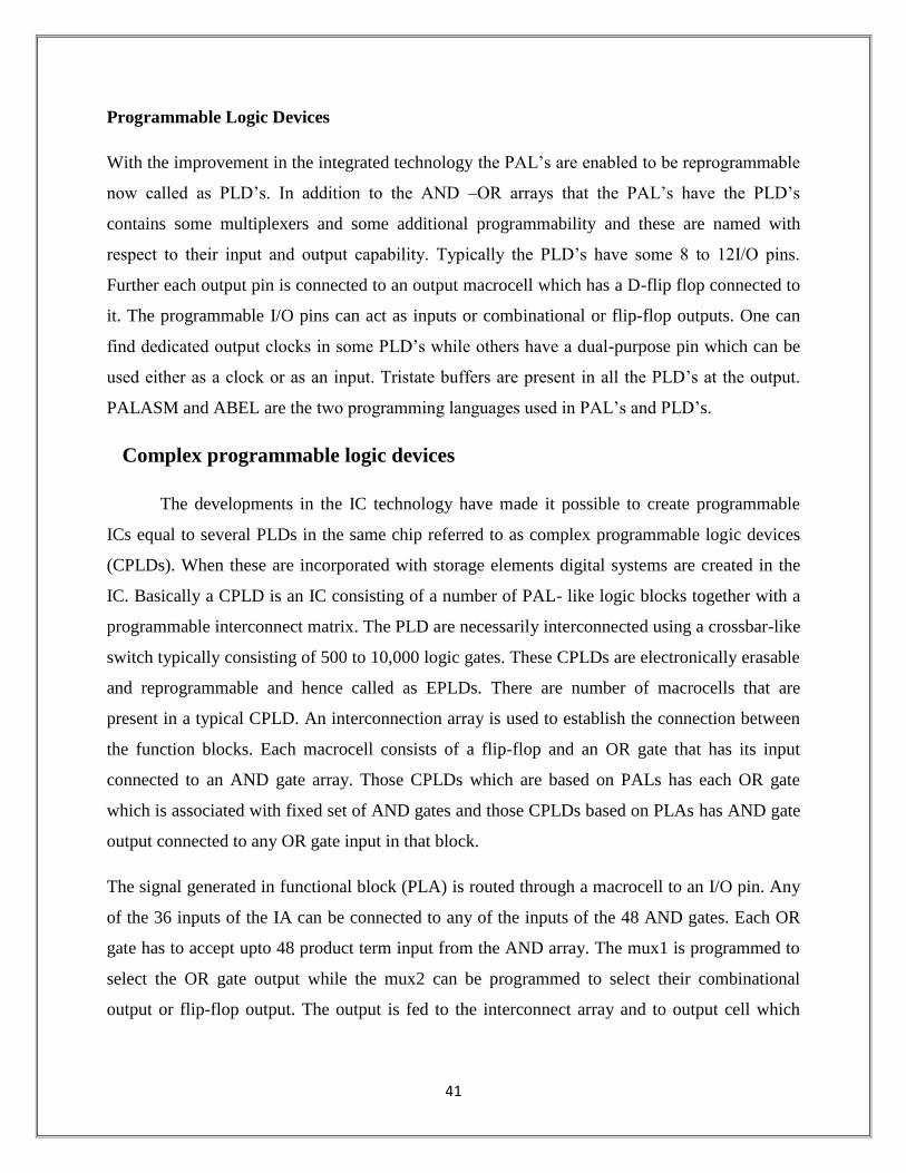
Programmable Logic Devices
With the improvement in the integrated technology the PAL’s are enabled to be reprogrammable
now called as PLD’s. In addition to the AND –OR arrays that the PAL’s have the PLD’s
contains some multiplexers and some additional programmability and these are named with
respect to their input and output capability. Typically the PLD’s have some 8 to 12I/O pins.
Further each output pin is connected to an output macrocell which has a D-flip flop connected to
it. The programmable I/O pins can act as inputs or combinational or flip-flop outputs. One can
find dedicated output clocks in some PLD’s while others have a dual-purpose pin which can be
used either as a clock or as an input. Tristate buffers are present in all the PLD’s at the output.
PALASM and ABEL are the two programming languages used in PAL’s and PLD’s.
Complex programmable logic devices
The developments in the IC technology have made it possible to create programmable
ICs equal to several PLDs in the same chip referred to as complex programmable logic devices
(CPLDs). When these are incorporated with storage elements digital systems are created in the
IC. Basically a CPLD is an IC consisting of a number of PAL- like logic blocks together with a
programmable interconnect matrix. The PLD are necessarily interconnected using a crossbar-like
switch typically consisting of 500 to 10,000 logic gates. These CPLDs are electronically erasable
and reprogrammable and hence called as EPLDs. There are number of macrocells that are
present in a typical CPLD. An interconnection array is used to establish the connection between
the function blocks. Each macrocell consists of a flip-flop and an OR gate that has its input
connected to an AND gate array. Those CPLDs which are based on PALs has each OR gate
which is associated with fixed set of AND gates and those CPLDs based on PLAs has AND gate
output connected to any OR gate input in that block.
The signal generated in functional block (PLA) is routed through a macrocell to an I/O pin. Any
of the 36 inputs of the IA can be connected to any of the inputs of the 48 AND gates. Each OR
gate has to accept upto 48 product term input from the AND array. The mux1 is programmed to
select the OR gate output while the mux2 can be programmed to select their combinational
output or flip-flop output. The output is fed to the interconnect array and to output cell which
42
includes the three-state buffer to drive the I/O pin. When the I/O is used as an input, the buffer
must be disabled.
Field programmable gate arrays
FPGAs are ICs which contain an array of identical logic blocks that are provided with
programmable interconnections. There are number of FPGA products available namely Xilinx,
Altera, lattice, actel, cypress. Arrays of programmable logic blocks are distributed within the
FPGA surrounded by input/output interface blocks. Basically there many types of programming
blocks like multiplexers and logic gates on one hand while some use only transistors. The
architecture also differs according to the use and purpose. The programmable blocks like logic
block, interconnect help to re-programme FPGA. In FPGA them interconnect can be
programmed to make or break connection. There might be different interconnects used
depending upon the FPGA company like general purpose interconnect, direct interconnect,
global lines and so on. StaticRAM programming technology, EPROM/EEPROM/flash
programming technology, Antifuse programming technology are the programming technologies
used to programme FPGA. In more recent times the vendors have incorporated embedded
processors, dedicated multipliers, analog-to-digital converters and so on in FPGAs.
VHDL SYNTHESIS ENVIRONMENT
Designer analyser. The design analyser is a user interface tool which has a command window
for the users in order to supply synthesis commands.
VHDL compiler. The compiler parses VHDL code, checks for syntax errors and checks for
VHDL construct in the code that are synthesizable. It also generates a summary report on the
components used.
Design compiler. The design is optimised by the design compiler based on the synthesis
constraints such as speed and area requirements.
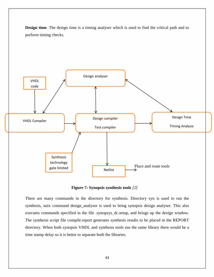
43
Design time. The design time is a timing analyser which is used to find the critical path and to
perform timing checks.
Place and route tools
Figure 7: Synopsis synthesis tools [2]
There are many commands in the directory for synthesis. Directory syn is used to run the
synthesis, unix command design_analyser is used to bring synopsis design analyser. This also
executes commands specified in the file .synopsys_dc.setup, and brings up the design window.
The synthesis script file compile.report generates synthesis results to be placed in the REPORT
directory. When both synopsis VHDL and synthesis tools use the same library there would be a
time stamp delay so it is better to separate both the libraries.
Design analyser
VHDL Compiler Design compiler
Test compiler
Design Time
Timing Analysis
Synthesis
technology
gate limited Netlist
VHDL
code

44
A synthesis technology library consists of definitions of basic components, operating conditions
and wire load models. Each component consists of its own logical function, timing, input pin
loading and output pin drive information. The synthesis usually uses library_name.sdb. The
command read/acct/synlib/Isi/lca300k.db can be used to read the synthesis technology inside the
designer analyser. It is important that we select a good synthesis library to match design
objectives such as speed requirements, cost, production schedule, and design tools.
REFERENCES
1. INTRODUCTION TO DIGITAL SYSTEMS: Modeling, Synthesis, and Simulation
Using VHDL Mohammed Ferdjallah
2. Digital systems design using VHDL Charles H.Roth, Lizy Kurian John
3. Digital systems design and VHDL synthesis K.C.Chang
4. Prof. A.Alkhalili Notes
5. Verilog HDL: A Guide to Digital Design and Synthesis, Second Edition Samir Palnitkar
6. VHDL Design Representation and Synthesis, Second Edition James R. Armstrong,
F. Gail Grey
Figures
[1] Digital systems design using VHDL Charles H.Roth, Lizy Kurian John
[2] Digital systems design and VHDL synthesis K.C.Chang
Examples and VHDL codes
?1? Digital systems design using VHDL Charles H.Roth, Lizy Kurian John
?2? VHDL Design Representation and Synthesis, Second Edition James R. Armstrong, F. Gail
?3? Prof. A.Alkhalili Notes
?4? Digital systems design and VHDL synthesis K.C.Chang

45
Fig. 1 Design Concept using VHDL
Design
VHDL coding
Synthesis
Target
layout
simulation
Test bench
ASIC vendor for fabrication