Embed Size (px)
Citation preview
Page 1/14
13March2012/version 7 LEM reserves the right to carry out modifications on its transducers, in order to improve them, without prior notice www.lem.com
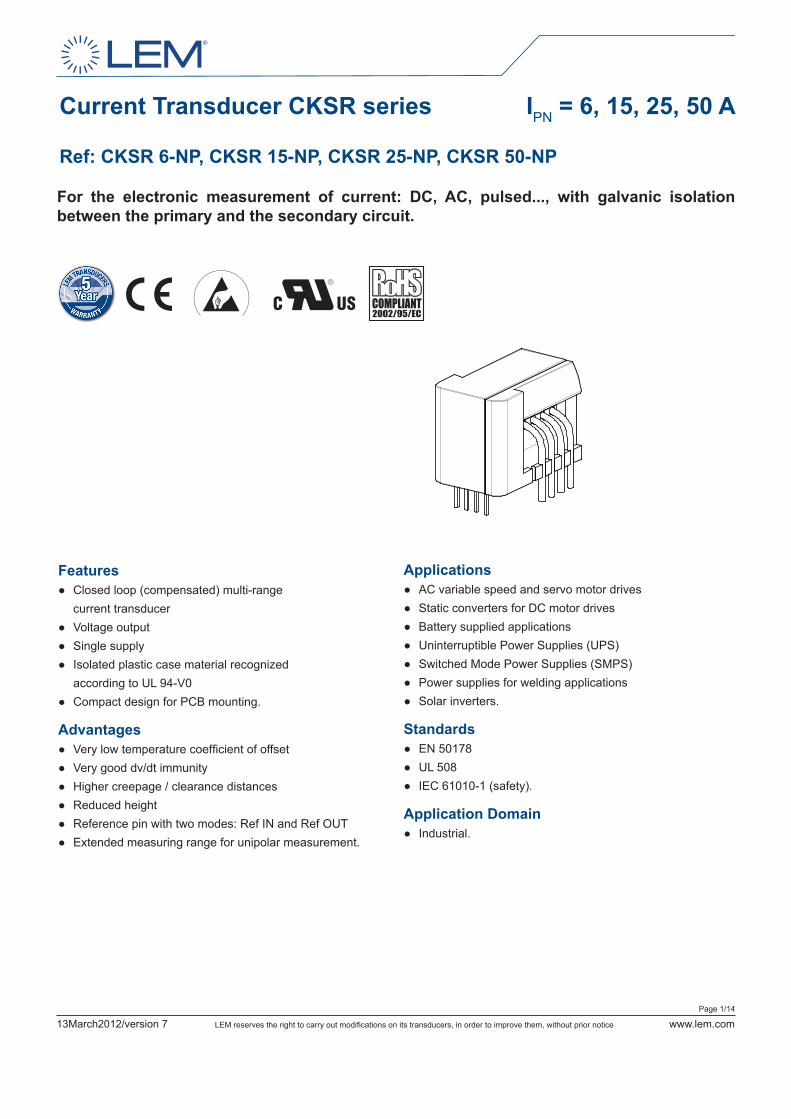
Current Transducer CKSR series IPN = 6, 15, 25, 50 A
Ref: CKSR 6-NP, CKSR 15-NP, CKSR 25-NP, CKSR 50-NP
For the electronic measurement of current: DC, AC, pulsed..., with galvanic isolation between the primary and the secondary circuit.
Features Closed loop (compensated) multi-range
current transducer Voltage output Single supply Isolated plastic case material recognized
according to UL 94-V0 Compact design for PCB mounting.
Advantages Very low temperature coefficient of offset Very good dv/dt immunity Higher creepage / clearance distances Reduced height Reference pin with two modes: Ref IN and Ref OUT Extended measuring range for unipolar measurement.
Applications AC variable speed and servo motor drives Static converters for DC motor drives Battery supplied applications Uninterruptible Power Supplies (UPS) Switched Mode Power Supplies (SMPS) Power supplies for welding applications Solar inverters.
Standards EN 50178 UL 508 IEC 61010-1 (safety).
Application Domain Industrial.

Page 2/14
13March2012/version 7 LEM reserves the right to carry out modifications on its transducers, in order to improve them, without prior notice www.lem.com
CKSR seriesAbsolute maximum ratings
Stresses above these ratings may cause permanent damage. Exposure to absolute maximum ratings for extended periods may degrade reliability.
Isolation characteristics
Parameter Symbol Unit Value Comment
RMS voltage for AC isolation test 50/60Hz/1 min Vd kV 4.3
Impulse withstand voltage 1.2/50 µs Vw kV 8
Partial discharge extinction voltage @ 10 pC (rms) Ve V 1000
Clearance distance (pri. - sec.) dCI mm 8.2 Shortest distance through air
Creepage distance (pri. - sec.) dCp mm 8.2 Shortest internal path along device body
Case material - - V0 according to UL 94
Comparative tracking index CTI V 600
Application example - - 300 V CAT III PD2
Reinforced isolation, non uniform field according to EN 61010
Application example - - 600 V CAT III PD2
Reinforced isolation, non uniform field according to EN 50178
Application example - - 1000 V CAT III PD2
Simple isolation, non uniform field according to EN 50178
According to UL 508: primary potential involved in Volts RMS AC or DC
- V 600For use in a pollution degree 2 environment
Environmental and mechanical characteristics
Parameter Symbol Unit Min Typ Max Comment
Ambient operating temperature TA°C -40 105
Ambient storage temperature TS°C -55 105
Mass m g 9
Standards EN 50178, IEC 60950-1, IEC 61010-1, IEC 61326-1, UL 508
Parameter Symbol Unit Value
Supply voltage VCV 7
Primary conductor temperature °C 110
Maximum primary current IP max A 20 x IPN
ESD rating, Human Body Model (HBM) kV 4

Page 3/14
13March2012/version 7 LEM reserves the right to carry out modifications on its transducers, in order to improve them, without prior notice www.lem.com
CKSR series
Parameter Symbol Unit Min Typ Max Comment
Primary nominal current rms IPN A 6 Apply derating according to fig. 25
Primary current, measuring range IPMA -20 20
Number of primary turns NP- 1,2,3,4
Supply voltage VCV 4.75 5 5.25
Current consumption IC mA 15 + 20 + NS = 1731 turns
Reference voltage @ IP = 0 A VREFV 2.495 2.5 2.505 Internal reference
External reference voltage VREFV 0 4
Output voltage VOUTV 0.375 4.625
Output voltage @ IP = 0 A VOUTV VREF
Electrical offset voltageVOE mV -5.3 5.3
100% tested VOUT - VREF
Electrical offset current referred to primary IOE mA -51 51 100% tested
Temperature coefficient of VREF TCVREF ppm/K ±5 ±50 Internal reference
Temperature coefficient of VOUT @ IP = 0 A
TCVOUT ppm/K ±6 ±14ppm/K of 2.5 V - 40°C .. 105°C
Theoretical sensitivity Gth mV/A 104.2 625 mV/ IPN
Sensitivity error εG% -0.7 0.7 100% tested
Temperature coefficient of G TCG ppm/K ±40 - 40°C .. 105°C
Linearity error εL% of IPN -0.1 0.1
Magnetic offset current (10 x IPN) referred to primary IOM A -0.1 0.1
Output current noise (spectral density) rms100 Hz .. 100 kHz referred to primary
inoµA/Hz½ 20 RL = 1 kΩ
Peak-peak output ripple at oscillator frequency f = 450 kHz (typ.)
- mV 40 160 RL = 1 kΩ
Reaction time @ 10 % of IPN tra µs 0.3 RL = 1 kΩ, di/dt = 18 A/µs
Response time @ 90 % of IPN tr µs 0.3 RL = 1 kΩ, di/dt = 18 A/µs
Frequency bandwidth (± 1 dB) BW kHz 200 RL = 1 kΩ
Frequency bandwidth (± 3 dB) BW kHz 300 RL = 1 kΩ
Overall accuracy XG % of IPN 1.7
Overall accuracy @ TA = 85°C (105°C) XG % of IPN 2.2
Accuracy X % of IPN 0.8
Accuracy @ TA = 85°C (105°C) X % of IPN 1.4
Electrical data CKSR 6-NPAt TA = 25°C, VC = + 5 V, NP = 1 turn, RL = 10 kΩ, internal reference, unless otherwise noted.
IP (mA) NS
IP (mA) NS
Page 4/14
13March2012/version 7 LEM reserves the right to carry out modifications on its transducers, in order to improve them, without prior notice www.lem.com
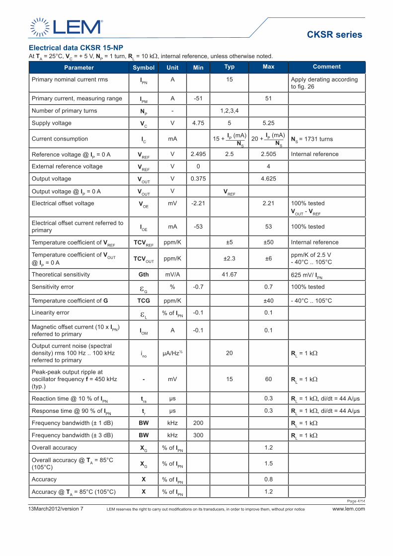
CKSR seriesElectrical data CKSR 15-NPAt TA = 25°C, VC = + 5 V, NP = 1 turn, RL = 10 kΩ, internal reference, unless otherwise noted.
Parameter Symbol Unit Min Typ Max Comment
Primary nominal current rms IPNA 15 Apply derating according
to fig. 26
Primary current, measuring range IPMA -51 51
Number of primary turns NP- 1,2,3,4
Supply voltage VCV 4.75 5 5.25
Current consumption IC mA 15 + 20 + NS = 1731 turns
Reference voltage @ IP = 0 A VREFV 2.495 2.5 2.505 Internal reference
External reference voltage VREFV 0 4
Output voltage VOUTV 0.375 4.625
Output voltage @ IP = 0 A VOUTV VREF
Electrical offset voltage VOEmV -2.21 2.21 100% tested
VOUT - VREF
Electrical offset current referred to primary IOE mA -53 53 100% tested
Temperature coefficient of VREF TCVREF ppm/K ±5 ±50 Internal reference
Temperature coefficient of VOUT @ IP = 0 A
TCVOUT ppm/K ±2.3 ±6 ppm/K of 2.5 V - 40°C .. 105°C
Theoretical sensitivity Gth mV/A 41.67 625 mV/ IPN
Sensitivity error εG% -0.7 0.7 100% tested
Temperature coefficient of G TCG ppm/K ±40 - 40°C .. 105°C
Linearity error εL% of IPN
-0.1 0.1
Magnetic offset current (10 x IPN) referred to primary IOM A -0.1 0.1
Output current noise (spectral density) rms 100 Hz .. 100 kHz referred to primary
ino µA/Hz½ 20 RL = 1 kΩ
Peak-peak output ripple at oscillator frequency f = 450 kHz (typ.)
- mV 15 60 RL = 1 kΩ
Reaction time @ 10 % of IPN tra µs 0.3 RL = 1 kΩ, di/dt = 44 A/µs
Response time @ 90 % of IPN tr µs 0.3 RL = 1 kΩ, di/dt = 44 A/µs
Frequency bandwidth (± 1 dB) BW kHz 200 RL = 1 kΩ
Frequency bandwidth (± 3 dB) BW kHz 300 RL = 1 kΩ
Overall accuracy XG % of IPN 1.2
Overall accuracy @ TA = 85°C (105°C) XG % of IPN 1.5
Accuracy X % of IPN 0.8
Accuracy @ TA = 85°C (105°C) X % of IPN 1.2
IP (mA) NS
IP (mA) NS
Page 5/14
13March2012/version 7 LEM reserves the right to carry out modifications on its transducers, in order to improve them, without prior notice www.lem.com
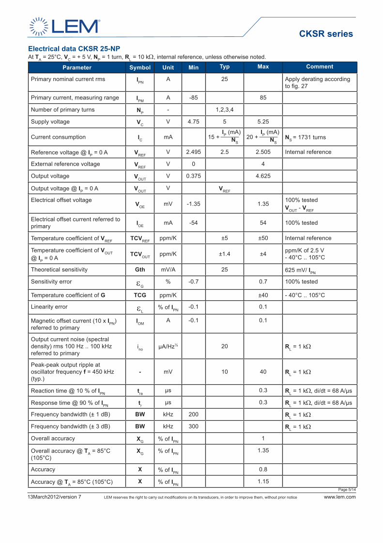
CKSR seriesElectrical data CKSR 25-NPAt TA = 25°C, VC = + 5 V, NP = 1 turn, RL = 10 kΩ, internal reference, unless otherwise noted.
Parameter Symbol Unit Min Typ Max Comment
Primary nominal current rms IPNA 25 Apply derating according
to fig. 27
Primary current, measuring range IPMA -85 85
Number of primary turns NP- 1,2,3,4
Supply voltage VCV 4.75 5 5.25
Current consumption IC mA 15 + 20 + NS = 1731 turns
Reference voltage @ IP = 0 A VREFV 2.495 2.5 2.505 Internal reference
External reference voltage VREFV 0 4
Output voltage VOUTV 0.375 4.625
Output voltage @ IP = 0 A VOUTV VREF
Electrical offset voltageVOE mV -1.35 1.35
100% tested VOUT - VREF
Electrical offset current referred to primary IOE mA -54 54 100% tested
Temperature coefficient of VREF TCVREF ppm/K ±5 ±50 Internal reference
Temperature coefficient of VOUT @ IP = 0 A
TCVOUT ppm/K ±1.4 ±4 ppm/K of 2.5 V - 40°C .. 105°C
Theoretical sensitivity Gth mV/A 25 625 mV/ IPN
Sensitivity error εG% -0.7 0.7 100% tested
Temperature coefficient of G TCG ppm/K ±40 - 40°C .. 105°C
Linearity error εL% of IPN
-0.1 0.1
Magnetic offset current (10 x IPN) referred to primary
IOMA -0.1 0.1
Output current noise (spectral density) rms 100 Hz .. 100 kHz referred to primary
ino µA/Hz½ 20 RL = 1 kΩ
Peak-peak output ripple at oscillator frequency f = 450 kHz (typ.)
- mV 10 40 RL = 1 kΩ
Reaction time @ 10 % of IPN traµs 0.3 RL = 1 kΩ, di/dt = 68 A/µs
Response time @ 90 % of IPN trµs 0.3 RL = 1 kΩ, di/dt = 68 A/µs
Frequency bandwidth (± 1 dB) BW kHz 200 RL = 1 kΩ
Frequency bandwidth (± 3 dB) BW kHz 300 RL = 1 kΩ
Overall accuracy XG % of IPN1
Overall accuracy @ TA = 85°C (105°C)
XG % of IPN1.35
Accuracy X % of IPN0.8
Accuracy @ TA = 85°C (105°C) X % of IPN1.15
IP (mA) NS
IP (mA) NS

Page 6/14
13March2012/version 7 LEM reserves the right to carry out modifications on its transducers, in order to improve them, without prior notice www.lem.com
CKSR series
Parameter Symbol Unit Min Typ Max Comment
Primary nominal current rms IPN A 50 Apply derating according to fig. 28
Primary current, measuring range IPM A -150 150
Number of primary turns NP - 1,2,3,4
Supply voltage VC V 4.75 5 5.25
Current consumption IC mA 15 + 20 + NS = 966 turns
Reference voltage @ IP = 0 A VREF V 2.495 2.5 2.505 Internal reference
External reference voltage VREF V 0 4
Output voltage VOUT V 0.375 4.625
Output voltage @ IP = 0 A VOUT V VREF
Electrical offset voltage VOE mV -0.725 0.725100% tested VOUT - VREF
Electrical offset current referred to primary IOE mA -58 58 100% tested
Temperature coefficient of VREF TCVREF ppm/K ±5 ±50 Internal reference
Temperature coefficient of VOUT @ IP = 0 A
TCVOUT ppm/K ±0.7 ±3 ppm/K of 2.5 V - 40°C .. 105°C
Theoretical sensitivity Gth mV/A 12.5 625 mV/ IPN
Sensitivity error εG% -0.7 0.7 100% tested
Temperature coefficient of G TCG ppm/K ±40 - 40°C .. 105°C
Linearity error εL% of IPN
-0.1 0.1
Magnetic offset current (10 x IPN) referred to primary IOM A -0.1 0.1
Output current noise (spectral density) rms 100 Hz .. 100 kHz referred to primary
ino µA/Hz½ 20 RL = 1 kΩ
Peak-peak output ripple at oscillator frequency f = 450 kHz (typ.)
- mV 5 20 RL = 1 kΩ
Reaction time @ 10 % of IPN tra µs 0.3 RL = 1 kΩ, di/dt = 100 A/µs
Response time @ 90 % of IPN trµs 0.3 RL = 1 kΩ, di/dt = 100 A/µs
Frequency bandwidth (± 1 dB) BW kHz 200 RL = 1 kΩ
Frequency bandwidth (± 3 dB) BW kHz 300 RL = 1 kΩ
Overall accuracy XG % of IPN0.9
Overall accuracy @ TA = 85°C (105°C)
XG % of IPN1.2
Accuracy X % of IPN0.8
Accuracy @ TA = 85°C (105°C) X % of IPN1.1
Electrical data CKSR 50-NPAt TA = 25°C, VC = + 5 V, NP = 1 turn, RL = 10 kΩ, internal reference, unless otherwise noted.
IP (mA) NS
IP (mA) NS
Page 7/14
13March2012/version 7 LEM reserves the right to carry out modifications on its transducers, in order to improve them, without prior notice www.lem.com
CKSR series
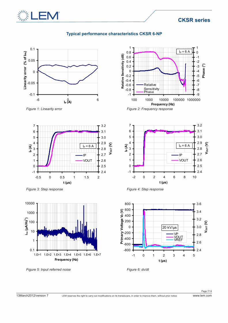
Typical performance characteristics CKSR 6-NP
Figure 1: Linearity error Figure 2: Frequency response
Figure 3: Step response Figure 4: Step response
Figure 5: Input referred noise Figure 6: dv/dt
-1-0.8-0.6-0.4-0.2
00.20.40.60.8
1
100 1000 10000 100000 1000000Frequency (Hz)
Rel
ativ
e Se
nsiti
vity
(dB
)
-9-8-7-6-5-4-3-2-101
Phas
e (°
)
RelativeSensitivityPhase
IP = 6 A
-1
0
1
2
3
4
5
6
7
-0.5 0 0.5 1 1.5 2t (µs)
I P (A
)
2.4
2.5
2.6
2.7
2.8
2.9
3.0
3.1
3.2
V OU
T (V)
IPVOUT
IP = 6 A
-1
0
1
2
3
4
5
6
7
-2 0 2 4 6 8 10t (µs)
I P (A
)
2.4
2.5
2.6
2.7
2.8
2.9
3.0
3.1
3.2
V OU
T (V)
IPVOUT
IP = 6 A
-0.1
-0.05
0
0.05
0.1
-6 0 6IP (A)
Line
arity
err
or (
% o
f I PN
)
-800
-600
-400
-200
0
200
400
600
800
-1 0 1 2 3 4 5t (µs)
Prim
ary
Volta
ge V
P (V)
2.4
2.6
2.8
3.0
3.2
3.4
3.6V O
UT (
V)
VPVOUTVREF
20 kV/μs
0.1
1
10
100
1000
10000
1.E+1 1.E+2 1.E+3 1.E+4 1.E+5 1.E+6 1.E+7Frequency (Hz)
i no (μ
A/H
z½)
Page 8/14
13March2012/version 7 LEM reserves the right to carry out modifications on its transducers, in order to improve them, without prior notice www.lem.com
CKSR series
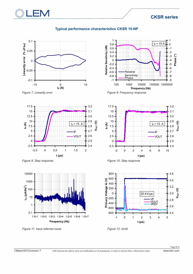
Typical performance characteristics CKSR 15-NP
Figure 7: Linearity error Figure 8: Frequency response
Figure 9: Step response Figure 10: Step response
Figure 11: Input referred noise Figure 12: dv/dt
-0.1
-0.05
0
0.05
0.1
-15 0 15IP (A)
Line
arity
err
or (
% o
f I PN
)
-1-0.8-0.6-0.4-0.2
00.20.40.60.8
1
100 1000 10000 100000 1000000Frequency (Hz)
Rel
ativ
e Se
nsiti
vity
(dB
)
-9-8-7-6-5-4-3-2-101
Phas
e (°
)
RelativeSensitivityPhase
IP = 15 A
-800
-600
-400
-200
0
200
400
600
800
-1 0 1 2 3 4 5t (µs)
Prim
ary
Volta
ge V
P (V)
2.4
2.6
2.8
3.0
3.2
3.4
3.6V O
UT (
V)
VPVOUTVREF
20 kV/μs
-2.5
0
2.5
5
7.5
10
12.5
15
17.5
-0.5 0 0.5 1 1.5 2
t (µs)
I P (A
)
2.4
2.5
2.6
2.7
2.8
2.9
3.0
3.1
3.2
V OU
T (V)
IPVOUT
IP = 15 A
-2.5
0
2.5
5
7.5
10
12.5
15
17.5
-2 0 2 4 6 8 10
t (µs)
I P (A
)
2.4
2.5
2.6
2.7
2.8
2.9
3.0
3.1
3.2
V OU
T (V)
IPVOUT
IP = 15 A
0.1
1
10
100
1000
10000
1.E+1 1.E+2 1.E+3 1.E+4 1.E+5 1.E+6 1.E+7
Frequency (Hz)
i no (μ
A/H
z½)
Page 9/14
13March2012/version 7 LEM reserves the right to carry out modifications on its transducers, in order to improve them, without prior notice www.lem.com
CKSR series
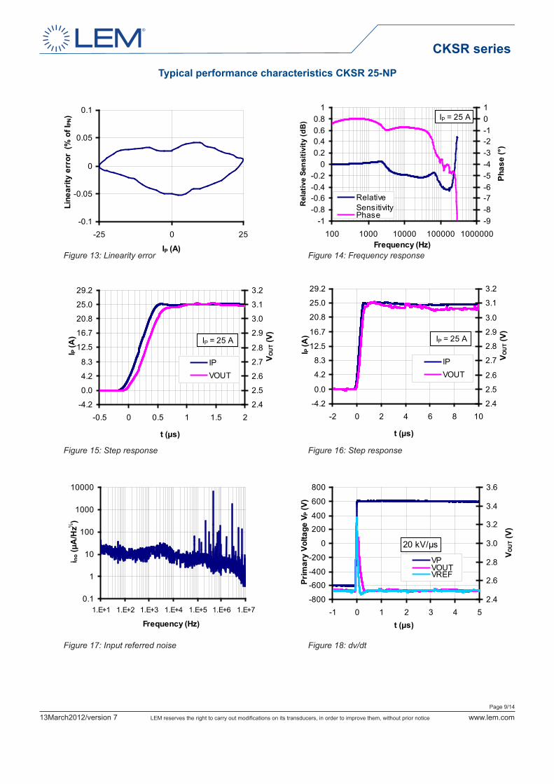
Typical performance characteristics CKSR 25-NP
Figure 13: Linearity error Figure 14: Frequency response
Figure 15: Step response Figure 16: Step response
Figure 17: Input referred noise Figure 18: dv/dt
-0.1
-0.05
0
0.05
0.1
-25 0 25
IP (A)
Line
arity
err
or (
% o
f I PN
)
-1-0.8-0.6-0.4-0.2
00.20.40.60.8
1
100 1000 10000 100000 1000000Frequency (Hz)
Rel
ativ
e Se
nsiti
vity
(dB
)
-9-8-7-6-5-4-3-2-101
Phas
e (°
)
RelativeSensitivityPhase
IP = 25 A
-4.2
0.0
4.2
8.3
12.5
16.7
20.8
25.0
29.2
-0.5 0 0.5 1 1.5 2
t (µs)
I P (A
)
2.4
2.5
2.6
2.7
2.8
2.9
3.0
3.1
3.2
V OU
T (V)
IPVOUT
IP = 25 A
-4.2
0.0
4.2
8.3
12.5
16.7
20.8
25.0
29.2
-2 0 2 4 6 8 10
t (µs)
I P (A
)
2.4
2.5
2.6
2.7
2.8
2.9
3.0
3.1
3.2
V OU
T (V)
IPVOUT
IP = 25 A
-800
-600
-400
-200
0
200
400
600
800
-1 0 1 2 3 4 5t (µs)
Prim
ary
Volta
ge V
P (V)
2.4
2.6
2.8
3.0
3.2
3.4
3.6
V OU
T (V)
VPVOUTVREF
20 kV/μs
0.1
1
10
100
1000
10000
1.E+1 1.E+2 1.E+3 1.E+4 1.E+5 1.E+6 1.E+7
Frequency (Hz)
i no (μ
A/H
z½)

Page 10/14
13March2012/version 7 LEM reserves the right to carry out modifications on its transducers, in order to improve them, without prior notice www.lem.com
CKSR seriesTypical performance characteristics CKSR 50-NP
Figure 19: Linearity error Figure 20: Frequency response
Figure 21: Step response Figure 22: Step response
Figure 23: Input referred noise Figure 24: dv/dt
-0.1
-0.05
0
0.05
0.1
-50 0 50
IP (A)
Line
arity
err
or (
% o
f I PN
)
-1-0.8-0.6-0.4-0.2
00.20.40.60.8
1
100 1000 10000 100000 1000000Frequency (Hz)
Rel
ativ
e Se
nsiti
vity
(dB
)
-9-8-7-6-5-4-3-2-101
Phas
e (°
)
RelativeSensitivityPhase
IP = 50 A
-800
-600
-400
-200
0
200
400
600
800
-1 0 1 2 3 4 5t (µs)
Prim
ary
Volta
ge V
P (V)
2.4
2.6
2.8
3.0
3.2
3.4
3.6
V OU
T (V)
VPVOUTVREF
20 kV/μs
-8.3
0.0
8.3
16.7
25.0
33.3
41.7
50.0
58.3
-0.5 0 0.5 1 1.5 2
t (µs)
I P (A
)
2.4
2.5
2.6
2.7
2.8
2.9
3.0
3.1
3.2
V OU
T (V)
IPVOUT
IP = 50 A
-8.3
0.0
8.3
16.7
25.0
33.3
41.7
50.0
58.3
-2 0 2 4 6 8 10
t (µs)
I P (A
)
2.4
2.5
2.6
2.7
2.8
2.9
3.0
3.1
3.2
V OU
T (V)
IPVOUT
IP = 50 A
0.1
1
10
100
1000
10000
1.E+1 1.E+2 1.E+3 1.E+4 1.E+5 1.E+6 1.E+7
Frequency (Hz)
i no (μ
A/H
z½)
Page 11/14
13March2012/version 7 LEM reserves the right to carry out modifications on its transducers, in order to improve them, without prior notice www.lem.com
CKSR series
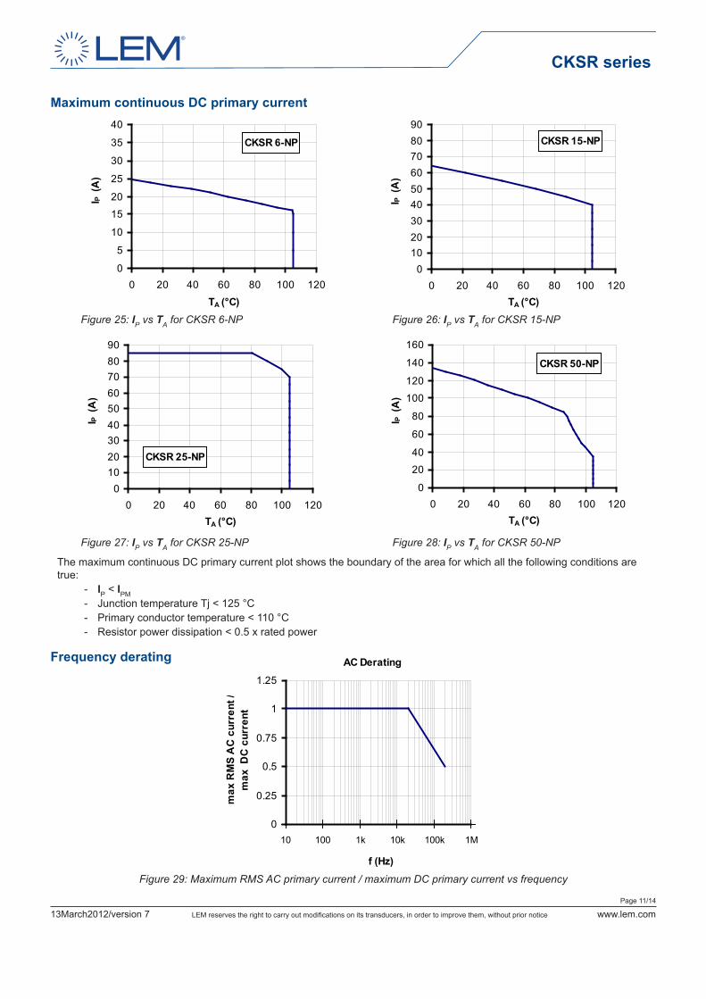
Maximum continuous DC primary current
Figure 25: IP vs TA for CKSR 6-NP Figure 26: IP vs TA for CKSR 15-NP
Figure 27: IP vs TA for CKSR 25-NP Figure 28: IP vs TA for CKSR 50-NP
The maximum continuous DC primary current plot shows the boundary of the area for which all the following conditions are true:
- IP < IPM - Junction temperature Tj < 125 °C - Primary conductor temperature < 110 °C - Resistor power dissipation < 0.5 x rated power
Frequency derating
Figure 29: Maximum RMS AC primary current / maximum DC primary current vs frequency
CKSR 6-NP
0
5
10
15
20
25
30
35
40
0 20 40 60 80 100 120
TA (°C)
I P (
A)
CKSR 15-NP
0102030405060708090
0 20 40 60 80 100 120TA (°C)
I P (
A)
CKSR 25-NP
0102030405060708090
0 20 40 60 80 100 120TA (°C)
I P (
A)
CKSR 50-NP
0
20
40
60
80
100
120
140
160
0 20 40 60 80 100 120TA (°C)
I P (
A)
AC Derating
10 100 1M1k 10k 100k0
0.25
0.5
0.75
1
1.25
f (Hz)
max
RM
S A
C c
urre
nt /
m
ax D
C c
urre
nt
Page 12/14
13March2012/version 7 LEM reserves the right to carry out modifications on its transducers, in order to improve them, without prior notice www.lem.com
Ampere-turns and amperesThe transducer is sensitive to the primary current linkage QP (also called ampere-turns).
QP=NPIP(At)
Where NPIP is the number of primary turn (1, 2 , 3 or 4 depending on the connection of the primary jumpers)
Caution: As most applications will use the transducer with only one single primary turn (NP = 1), much of this datasheet is written in terms of primary current instead of current linkages. However, the ampere-turns (A-t) unit is used to emphasis that current linkages are intended and applicable.
Transducer simplified modelThe static model of the transducer at temperature TA is:VOUT = G QP + error
In which error = VOE + VOT (TA) + εG ·QP·G + εL(QPmax)·QPmax·G + TCG·(TA-25)·QP·G
With: QP = NPIP :the input ampere-turns (At) Please read above warning. QPmax :the maxi input ampere-turns that have been applied to the transducer (At) VOUT :the secondary voltage (V) TA :the ambient temperature (°C) VOE :the electrical offset voltage (V) VOT(TA) :the temperature variation of VO at temperature TA (V) G :the sensitivity of the transducer (V/At) εG :the sensitivity error εL (QPmax) :the linearity error for QPmax
This model is valid for primary ampere-turns QP between -QPmax and +QPmax only.
Performance parameters definition
Sensitivity and linearityTo measure sensitivity and linearity, the primary current (DC) is cycled from 0 to IP, then to -IP and back to 0 (equally spaced IP/10 steps).The sensitivity G is defined as the slope of the linear regres-sion line for a cycle between ± IPN.
The linearity error εL is the maximum positive or negativedifference between the measured points and the linearregression line, expressed in % of IPN.
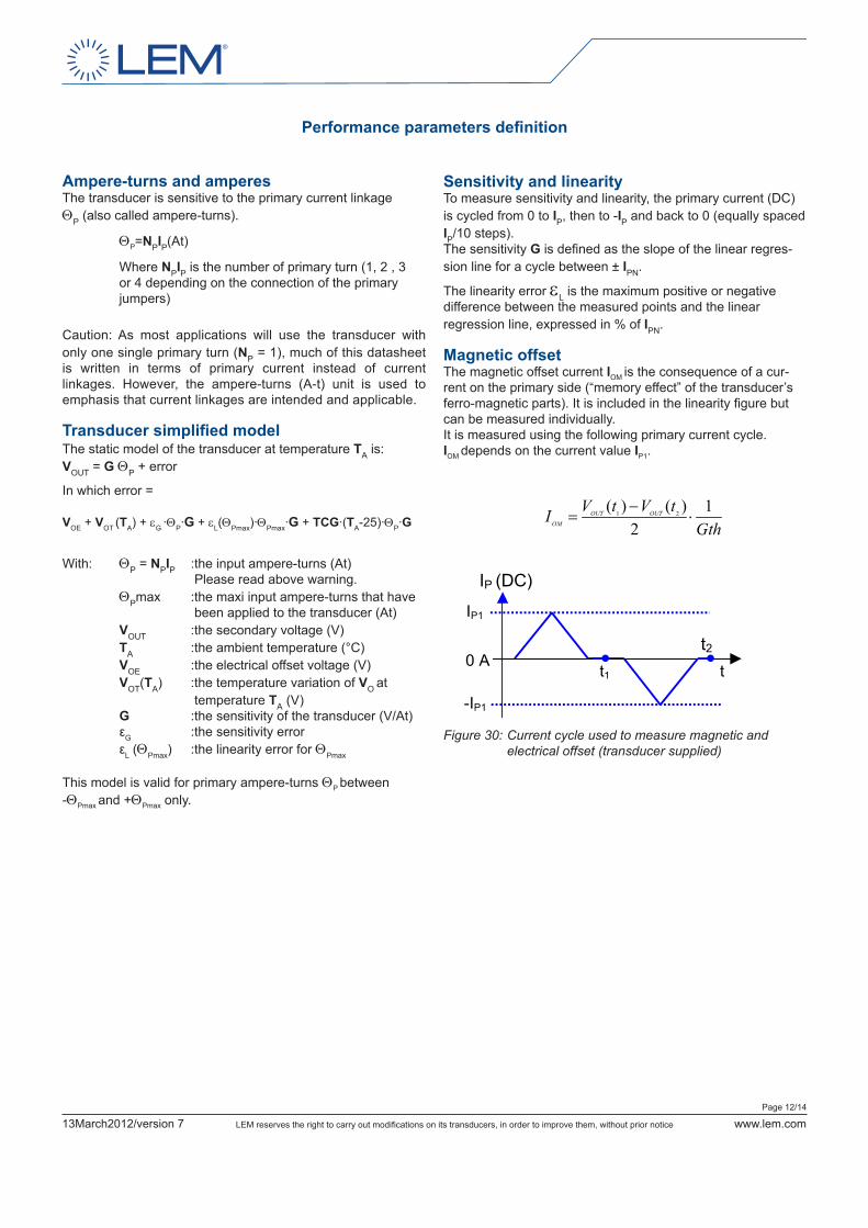
Magnetic offsetThe magnetic offset current IOM is the consequence of a cur-rent on the primary side (“memory effect” of the transducer’s ferro-magnetic parts). It is included in the linearity figure but can be measured individually.It is measured using the following primary current cycle.IOM depends on the current value IP1.
Figure 30: Current cycle used to measure magnetic and electrical offset (transducer supplied)
IP (DC)
-IP1
IP1
0 A t1 t t Ip(3)
t2 Ip(3)
GthtVtVI OUTOUT
OM
12
)()(21 ⋅
−=
Page 13/14
13March2012/version 7 LEM reserves the right to carry out modifications on its transducers, in order to improve them, without prior notice www.lem.com
CKSR series
Electrical offsetThe electrical offset voltage VOE can either be measured when the ferro-magnetic parts of the transducer are:
completely demagnetized, which is difficult to realize, or in a known magnetization state, like in the current cycle
shown in figure 30. Using the current cycle shown in figure 30, the electrical offset is: The temperature variation VOT of the electrical offset voltage VOE is the variation of the electrical offset from 25°C to the considered temperature: Note: the transducer has to be demagnetized prior to the application of the current cycle (for example with a demagnetization tunnel).
Figure 31: Test connection
Overall accuracyThe overall accuracy at 25°C XG is the error in the - IPN .. + IPN range, relative to the rated value IPN.
It includes:
the electrical offset VOE the sensitivity error εG the linearity error εL (to IPN)
The magnetic offset is part of the overall accuracy. It is taken into account in the linearity error figure provided the transducer has not been magnetized by a current higher than IPN.
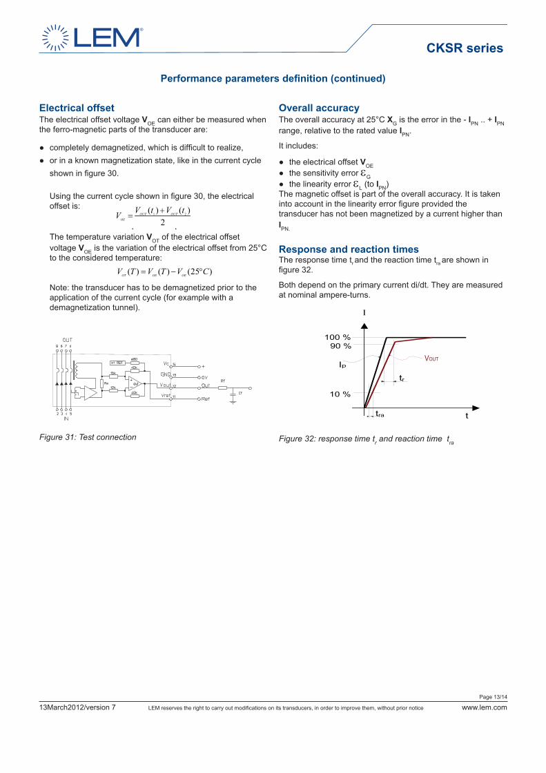
Response and reaction timesThe response time tr and the reaction time tra are shown in figure 32.
Both depend on the primary current di/dt. They are measured at nominal ampere-turns.
Figure 32: response time tr and reaction time tra
Performance parameters definition (continued)
2)()(
21tVtVV OUTOUT
OE
+=
)25()()( CVTVTVOEOEOT
°−=
tra
VOUT
tr
90 %
10 %
t
100 %
Ip
I
Page 14/14
13March2012/version 7 LEM reserves the right to carry out modifications on its transducers, in order to improve them, without prior notice www.lem.com
CKSR series
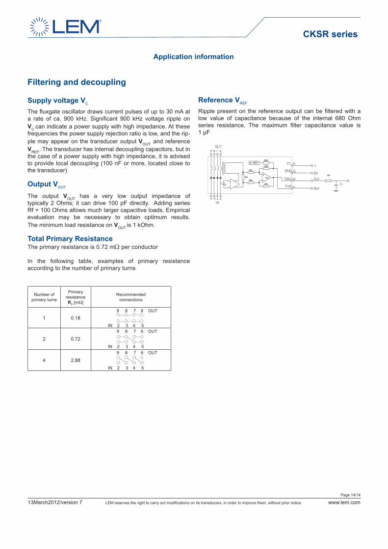
Filtering and decoupling
Supply voltage VC
The fluxgate oscillator draws current pulses of up to 30 mA at a rate of ca. 900 kHz. Significant 900 kHz voltage ripple on VC can indicate a power supply with high impedance. At these frequencies the power supply rejection ratio is low, and the rip-ple may appear on the transducer output VOUT and reference VREF. The transducer has internal decoupling capacitors, but in the case of a power supply with high impedance, it is advised to provide local decoupling (100 nF or more, located close to the transducer)
Output VOUT
The output VOUT has a very low output impedance of typically 2 Ohms; it can drive 100 pF directly. Adding series Rf = 100 Ohms allows much larger capacitive loads. Empirical evaluation may be necessary to obtain optimum results. The minimum load resistance on VOUT is 1 kOhm.
Total Primary ResistanceThe primary resistance is 0.72 mΩ per conductor In the following table, examples of primary resistance according to the number of primary turns
Application information
Reference VREF
Ripple present on the reference output can be filtered with a low value of capacitance because of the internal 680 Ohm series resistance. The maximum filter capacitance value is 1 µF
Number ofprimary turns
PrimaryresistanceRP [mW]
Recommendedconnections
1 0.18 9 8 7 6 OUT
IN 2 3 4 5
2 0.72 9 8 7 6 OUT
IN 2 3 4 5
4 2.88 9 8 7 6 OUT
IN 2 3 4 5
Page 15/14
13March2012/version 7 LEM reserves the right to carry out modifications on its transducers, in order to improve them, without prior notice www.lem.com
CKSR series
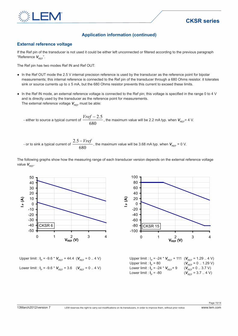
External reference voltage
If the Ref pin of the transducer is not used it could be either left unconnected or filtered according to the previous paragraph “Reference VREF”. The Ref pin has two modes Ref IN and Ref OUT:
In the Ref OUT mode the 2.5 V internal precision reference is used by the transducer as the reference point for bipolar measurements; this internal reference is connected to the Ref pin of the transducer through a 680 Ohms resistor. it tolerates sink or source currents up to ± 5 mA, but the 680 Ohms resistor prevents this current to exceed these limits.
In the Ref IN mode, an external reference voltage is connected to the Ref pin; this voltage is specified in the range 0 to 4 V and is directly used by the transducer as the reference point for measurements. The external reference voltage VREF must be able:
- either to source a typical current of 680
5.2−Vref, the maximum value will be 2.2 mA typ. when VREF= 4 V.
- or to sink a typical current of 680
5.2 Vref−, the maximum value will be 3.68 mA typ. when VREF = 0 V.
The following graphs show how the measuring range of each transducer version depends on the external reference voltage value VREF.
Upper limit : IP = -9.6 * VREF + 44.4 (VREF = 0 .. 4 V) Upper limit : IP = -24 * VREF + 111 (VREF = 1.29 .. 4 V) Upper limit : IP = 80 (VREF = 0 .. 1.29 V) Lower limit : IP = -9.6 * VREF + 3.6 (VREF = 0 .. 4 V) Lower limit : IP = -24 * VREF+ 9 (VREF= 0 .. 3.7 V) Lower limit : IP = -80 (VREF = 3.7 .. 4 V)
Application information (continued)
-50-40-30-20-10
01020304050
0 1 2 3 4VREF (V)
I P
(A)
CKSR 6-100
-80-60-40-20
020406080
100
0 1 2 3 4VREF (V)
I P
(A)
CKSR 15

Page 16/14
13March2012/version 7 LEM reserves the right to carry out modifications on its transducers, in order to improve them, without prior notice www.lem.com
CKSR seriesExternal reference voltage (continued)
Upper limit : IP = -40 * VREF+ 185 (VREF = 2.5 .. 4 V) Upper limit : IP = -80 * VREF + 370 (VREF = 2.75 .. 4 V) Upper limit : IP = 85 (VREF = 0 .. 2.5 V) Upper limit : IP = 150 (VREF = 0 .. 2.75 V) Lower limit : IP = -40 * VREF + 15 (VREF = 0 .. 2.5 V) Lower limit : IP = -80 * VREF + 30 (VREF= 0 .. 2.25 V) Lower limit : IP = -85 (VREF = 2.5 .. 4 V) Lower limit : IP = -150 (VREF = 2.25 .. 4 V)
Example with VREF = 1.65 V:
The 6 A version has a measuring range from - 12.24 A to + 28.5 A The 15 A version has a measuring range from - 30.6 A to + 71.4 A The 25 A version has a measuring range from - 51 A to + 85 A The 50 A version has a measuring range from - 102 A to + 150 A
Example with VREF = 0 V:
The 6 A version has a measuring range from + 3.6 A to + 44.4 A The 15 A version has a measuring range from + 9 A to + 80 A The 25 A version has a measuring range from + 15 A to + 85 A The 50 A version has a measuring range from + 30 A to + 150 A
-100-80-60-40-20
020406080
100
0 1 2 3 4VREF (V)
I P
(A)
CKSR 25-200
-150
-100
-50
0
50
100
150
200
0 1 2 3 4VREF (V)
I P
(A)
CKSR 50
Page 17/14
13March2012/version 7 LEM reserves the right to carry out modifications on its transducers, in order to improve them, without prior notice www.lem.com
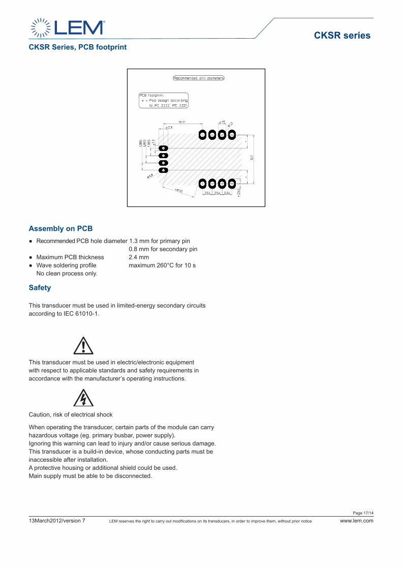
CKSR seriesCKSR Series, PCB footprint
Assembly on PCB Recommended PCB hole diameter 1.3 mm for primary pin
0.8 mm for secondary pin Maximum PCB thickness 2.4 mm Wave soldering profile maximum 260°C for 10 s
No clean process only.
Safety
This transducer must be used in limited-energy secondary circuits according to IEC 61010-1.
This transducer must be used in electric/electronic equipment with respect to applicable standards and safety requirements in accordance with the manufacturer’s operating instructions.
Caution, risk of electrical shock
When operating the transducer, certain parts of the module can carry hazardous voltage (eg. primary busbar, power supply). Ignoring this warning can lead to injury and/or cause serious damage. This transducer is a build-in device, whose conducting parts must be inaccessible after installation. A protective housing or additional shield could be used. Main supply must be able to be disconnected.
Page 18/14
13March2012/version 7 LEM reserves the right to carry out modifications on its transducers, in order to improve them, without prior notice www.lem.com
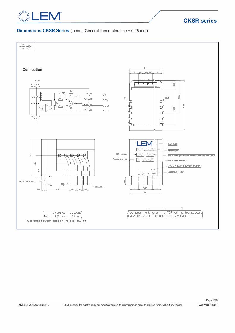
CKSR seriesDimensions CKSR Series (in mm. General linear tolerance ± 0.25 mm)
Connection