Embed Size (px)
Citation preview

1
Recent Developments in Compound Semiconductor
Microwave Power Transistor Technology
Christopher M. Snowden
Filtronic plc, Salts Mill Road, Shipley, BD18 3TT UK and School of Electronic and Electrical Engineering, The University of Leeds, LS2 9JT UK.
Email: [email protected]
Abstract. This paper addresses the state-of-the-art in microwave and millimetre-wave power
transistor technology. The relative performance of microwave power transistor technology
from 1 GHz to 60 GHz is reviewed. The fundamental technological drivers in the design of
microwave compound semiconductor power transistors are discussed as the basis for
developing optimum designs. A new high yield power GaAs pHEMT process is described and
the application of this technology to multi-carrier microwave power amplifiers is discussed,
achieving state-of-the-art performance, with output powers of up to 120 W with 70%
efficiency at 2.1 GHz.
1.0 INTRODUCTION
Solid-state microwave power amplifiers are required to deliver RF power levels between a
few Watts at millimeter-wave frequencies to peak powers of over a kilowatt at 1 GHz, in
communications and Radar applications. The design of high performance microwave power
amplifiers for future communications systems requires very low levels of distortion, high
efficiencies and the ability to handle multiple carriers whilst simultaneously operating at very
low levels of intermodulation distortion. The performance of the power amplifier depends
critically upon the choice of active device and the embedding circuit design. Recent high
efficiency designs, require power transistors with very high cut-off frequencies and very low
‘on’ resistances. This has led to an upsurge of interest in using compound semiconductor
2
transistors, and in particular pseudomorphic high electron mobility transistors (pHEMTs) and
heterojunction bipolar transistors (HBTs), which can achieve higher efficiencies and
improved linearity at these frequencies [1,2].
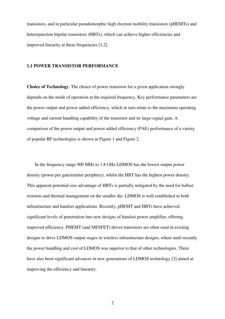
1.1 POWER TRANSISTOR PERFORMANCE
Choice of Technology. The choice of power transistor for a given application strongly
depends on the mode of operation at the required frequency. Key performance parameters are
the power output and power added efficiency, which in turn relate to the maximum operating
voltage and current handling capability of the transistor and its large-signal gain. A
comparison of the power output and power added efficiency (PAE) performance of a variety
of popular RF technologies is shown in Figure 1 and Figure 2.
In the frequency range 900 MHz to 1.8 GHz LDMOS has the lowest output power
density (power per gate/emitter periphery), whilst the HBT has the highest power density.
This apparent potential size advantage of HBTs is partially mitigated by the need for ballast
resistors and thermal management on the smaller die. LDMOS is well established in both
infrastructure and handset applications. Recently, pHEMT and HBTs have achieved
significant levels of penetration into new designs of handset power amplifier, offering
improved efficiency. PHEMT (and MESFET) driver transistors are often used in existing
designs to drive LDMOS output stages in wireless infrastructure designs, where until recently
the power handling and cost of LDMOS was superior to that of other technologies. There
have also been significant advances in new generations of LDMOS technology [3] aimed at
improving the efficiency and linearity.

3
Cellular infrastructure base station power amplifiers represent the largest market for high
power microwave transistors. Although LDMOS FETs are the most widely used technology
today in this application below 2 GHz, their relatively low unity gain cut-off frequency
(usually below 7 GHz), means that they struggle to simultaneously meet the efficiency and
linearity requirements for third-generation mobile communication systems operating above 2
GHz. Over the past three years very high power GaAs MESFETs, HFETs and PHEMTs have
demonstrated superior performance to LDMOS at these frequencies [4,5,6]. Until recently the
cost of compound semiconductor transistors has been significantly higher than that of
LDMOS. However, with a target price of less than $1/Watt for a packaged part, recent
developments in manufacturing technology (notably 6” GaAs wafers) promise competitive
pricing from compound semiconductor devices. A new high power, high yield GaAs FET
technology is described in this paper that satisfies the demanding performance required for
third-generation mobile communication power amplifiers. The cost of packaging remains a
substantial element of the final cost of discrete power transistors and this has led to the
development of higher levels of integration in multi-chip modular designs.
Other applications, such as Radar, have used both silicon bipolar and LDMOS devices at
lower frequencies (up to 4 GHz), but increasingly GaAs-based transistors (MESFETs,
HEMTs, HBTs) are being used to improve performance in these systems. Above 8 GHz, these
GaAs transistors are used exclusively at this time. Increased interest in electronically-scanned
(Escan) radars has led to the requirement for high efficiency power amplifier monolithic
microwave integrated circuits (MMICs). An 8 Watt, 10 GHz power amplifier for Escan radar
applications is shown in Figure 3, which was fabricated using the process described later in
this paper. At frequencies above 18 GHz, where power levels of few Watts are usually
required in applications such as Point-to-Point transceivers, HEMT MMIC technology is
dominant.
4
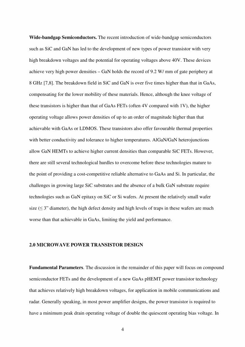
Wide-bandgap Semiconductors. The recent introduction of wide-bandgap semiconductors
such as SiC and GaN has led to the development of new types of power transistor with very
high breakdown voltages and the potential for operating voltages above 40V. These devices
achieve very high power densities – GaN holds the record of 9.2 W/ mm of gate periphery at
8 GHz [7,8]. The breakdown field in SiC and GaN is over five times higher than that in GaAs,
compensating for the lower mobility of these materials. Hence, although the knee voltage of
these transistors is higher than that of GaAs FETs (often 4V compared with 1V), the higher
operating voltage allows power densities of up to an order of magnitude higher than that
achievable with GaAs or LDMOS. These transistors also offer favourable thermal properties
with better conductivity and tolerance to higher temperatures. AlGaN/GaN heterojunctions
allow GaN HEMTs to achieve higher current densities than comparable SiC FETs. However,
there are still several technological hurdles to overcome before these technologies mature to
the point of providing a cost-competitive reliable alternative to GaAs and Si. In particular, the
challenges in growing large SiC substrates and the absence of a bulk GaN substrate require
technologies such as GaN epitaxy on SiC or Si wafers. At present the relatively small wafer
size (≤ 3” diameter), the high defect density and high levels of traps in these wafers are much
worse than that achievable in GaAs, limiting the yield and performance.
2.0 MICROWAVE POWER TRANSISTOR DESIGN
Fundamental Parameters. The discussion in the remainder of this paper will focus on compound
semiconductor FETs and the development of a new GaAs pHEMT power transistor technology
that achieves relatively high breakdown voltages, for application in mobile communications and
radar. Generally speaking, in most power amplifier designs, the power transistor is required to
have a minimum peak drain operating voltage of double the quiescent operating bias voltage. In

5
some modes of operation (such as Class E and Class F) this breakdown voltage may have to be up
to three times higher than the bias voltage. This provides a lower bound on the breakdown voltage.
It is necessary to recognise that in depletion-mode FETs, with negative gate bias voltages, that the
gate-drain peak voltage is usually the limiting factor in terms of breakdown. Although LDMOS,
SiC and GaN transistors can achieve breakdown voltages of over 60V or more, GaAs-based
transistors rarely exceed 25V for breakdown for VDSB or VDGB (determined for a given level of
gate current in GaAs FETs). This usually limits the DC supply to less than 12V for GaAs FETs. In
GaAs MESFETs and HEMTs the breakdown voltage is usually determined by the interaction of
surface geometry, surface material properties and active channel design. In particular, key
parameters are the gate-drain separation, the Schottky gate parameters including the built-in
potential, metallization and recess (single or double) and the drain-source channel parameters
(doping, material composition and layer thicknesses). Novel GaAs FET structures including
gamma gates (the shape of the gate metallization) and field-plate FETs have been reported, which
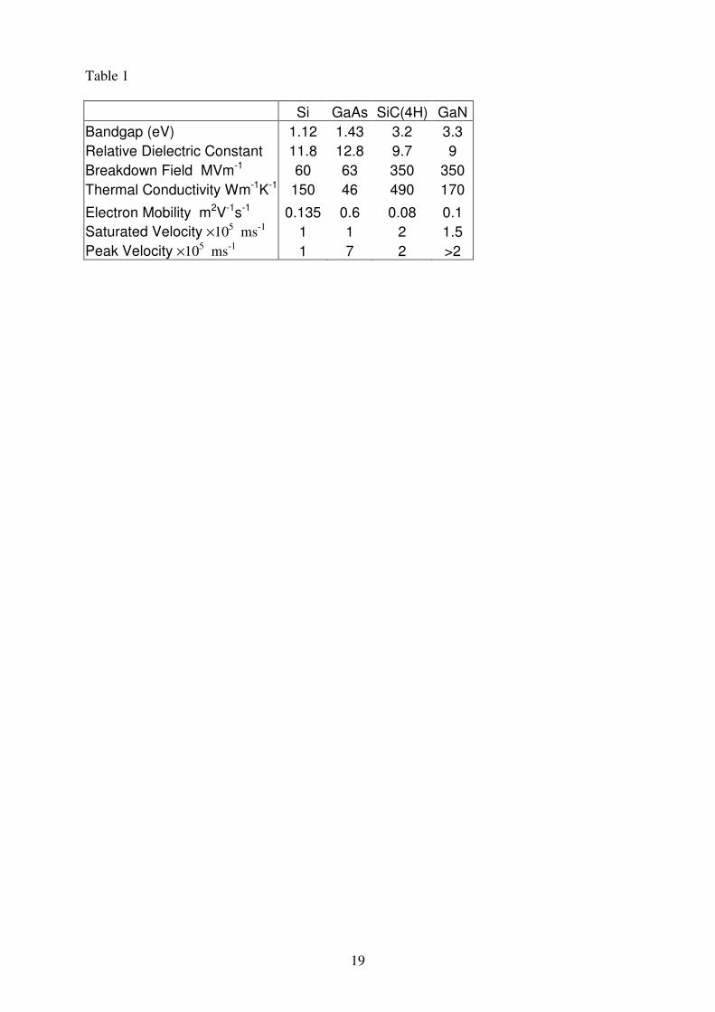
achieve breakdown voltages of over 100V [9]. An experimental gamma-gate structure, developed
for a pHEMT is shown in Figure 4. A disadvantage of this approach is that the cut-off frequency
of the FET is reduced as a consequence of the increased gate-drain capacitance. A power pHEMT
process with a ‘T’ gate structure and exceptionally good DC and microwave performance is
described later in this paper.
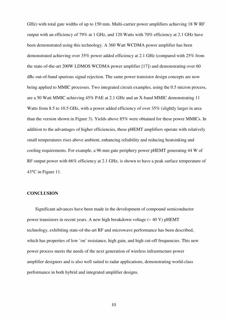
A key parameter in power FET design is the breakdown field, which limits the peak electric
field between the gate and drain, Table 1. The breakdown field is a strong function of the material
quality and the density of impurities (including the donors). Over the past ten years improvements
in GaAs material technology have led to an increase in the breakdown fields achievable in
practical structures and these now approach the theoretical limit.

6
The breakdown voltage in a GaAs power FET is maximised by careful design of the channel,
whilst employing double recess gate structures and appropriate passivation of the semiconductor
surface. The gate-drain spacing is optimized to maximize the breakdown voltage, whilst avoiding
excessive drain channel resistance. Surface states in GaAs and InP give rise to surface depletion,
which interacts with passivation layers causing unwanted surface leakage, breakdown, and
transient trapping phenomena that can manifest themselves as gate and drain lag effects.
The drain current (with a maximum value Imax at Vknee), knee voltage (Vknee) and gain in
microwave FETs is directly dependent on the electron mobility, velocity and electron density in
the conducting channel. GaAs has a mobility, which is over four times higher than that of Si and
achieves very high peak velocity over a short distance (velocity overshoot). Hence, in short gate
length GaAs-based power FETs the maximum current handling capacity per unit periphery is the
highest of all the semiconductor technologies considered here. Unfortunately, the mobility and
velocity decrease as the doping density increases (ie. as the current handling increases). This
problem can be overcome using in GaAs pHEMT structures with undoped channels and separate
highly doped supply layer (normally separated with a thin undoped spacer layer). However, the
desire for higher charge densities in the supply levels has to be balanced against the requirement to
maximize breakdown voltage, which also decreases with increasing doping level (due to impact or
avalanche ionisation).
Finally, it is important to consider the voltage swing required on both the gate and drain. In
addition to the limits imposed on the drain voltage by the knee voltage and the breakdown
voltage, it is necessary to consider the impact of the pinch-off voltage and gate conduction on
the gate voltage swing. Recently there has been a move towards circuit designers preferring
enhancement mode devices (e-mode), which only require positive gate bias voltages. These
devices tend to have a higher breakdown voltage and high gain, although the positive pinch-off

7
voltage Vpo coupled with the gate barrier height restrict the useful voltage swing to usually less
than 0.5V and gate-leakage currents may be problematic in some designs. In contrast a
depletion-mode (d-mode) device or quasi-emode (Vpo ~ -0.5V), allow larger gate voltage
swings and reduced gate leakage. The pinch-off voltage itself is a function of charge density
(doping) and epitaxial channel layer thickness. The MESFET and HEMT, like other FETs, are
charge-control devices, where the gate charge and gate capacitance are a strong non-linear
functions of gate potential. The charge-control mechanism, together with the drain and source
bias determines the drain–source current. The non-linear behaviour of the capacitances can
have a significant impact on the operation of power amplifiers under large-signal conditions
and must be considered during the design of the transistor and its embedding circuit.
2.1 ELECTRO-THERMAL MODELLING AND DESIGN
The performance of new power transistor designs can be assessed using physical device
models in conjunction with time domain simulators to study directly large-signal behaviour
[10,11], including intermodulation distortion (within the limitations of lengthy time-domain
simulation for this type of signal) [14]. During the past ten years, a fast class of simulation
tool known as a ‘quasi-two-dimensional (Q2D) model’, has allowed relatively accurate results
to be obtained in a small fraction of the time consumed by traditional two-dimensional
models. The microwave power FET development described here has made use of the
thermally self-consistent Leeds Physical Model (LPM), which is a fast fully physical Q2D
simulator, with the capability of providing large signal time-domain data and allowing CAD
timescale simulations [11,12,13,14].
A typical power pHEMT structure investigated in this work is shown in Figure 5. In these
devices, many of the layers in the device structure are very thin (< 100 Å) and often form

8
heterostructure interfaces where quantization of the electron energy occurs, such as in the FET
channel. The LPM model uses a self-consistent quantum mechanical model to represent the gate
charge-control model [13]. In addition to its role in the full device model, this charge-control
model has been used to investigate the epitaxial layer design. An example of a conduction energy-
band diagram for a pHEMT epitaxial structure is shown in Figure 6. This clearly shows the
‘rectangular’ well, characteristic of InGaAs pHEMTs, showing the quantized electron energy
levels. This profile has been designed to minimize parasitic conduction between the gate metal and
the channel (the ‘well’).
The strong temperature dependence of electron mobility and relatively poor thermal conductivity
of GaAs requires an accurate thermal model that can be coupled self-consistently to the electrical
model of the transistor. Thermal modeling in this work has utilized a dynamic self-consistent thermal
impedance matrix model of non-linear heat flow for the full power FET die [10,14,16], supported by
infra-red measurements. A simulated temperature profile, from the models used in this work, for a
cross-section through a power FET is shown in Figure 7, where peaks in the temperature correspond
with the regions in the FET channel at the drain edge of the gate fingers. It has been shown that
detailed device structure, including the device contact finger layout, surface metallisation and vias,
all impact on the transient thermal response [16]. Also, thermal time constants can vary by several
orders of magnitude, depending on the scale of power dissipation and temperature sensitive areas and
volumes. This analysis provides valuable insight for thermal design.
Equivalent circuit modeling, based on extraction of model parameters from measured data, plays a
key role in characterizing the devices and process. Passive elements, including via holes (used to
ground the source contacts in the power FETs), have been characterized using this technique. Non-
linear model elements based on extraction from multi-frequency, bias-dependent S parameter
measurements form the basis of the FET intrinsic equivalent circuit model.

9
3.0 A VERY HIGH PERFORMANCE POWER FET TECHNOLOGY
A high yield power pHEMT technology, based on an InGaAs/AlGaAs/GaAs molecular beam
epitaxy layer structure, has been developed to support microwave power amplifier applications
with single die capable of handling RF powers of up to 75W. Several novel processes were
developed to fabricate these devices on 6” GaAs wafers, including a low resistance ‘T’ gate
structure with silicon nitride SiN passivation, Figure 8. Both 0.5 µm and 0.25 µm gate length
versions have been developed, where the ‘T’ gate sits in a dry-etch defined gate recess. The 0.5
µm gate exhibits a gate resistance of less than 38 Ω/mm. Excellent pinch-off uniformity is
maintained by a high selectivity etch-stop layer. A specially developed multi-layer surface
passivation process allows a high breakdown voltage to be obtained, whilst reducing dispersion in
the current-voltage characteristics to a very low level. The finished 6” wafers are thinned (in-situ)
to ensure good thermal performance and minimal via hole impedance, Figure 9. Via hole
resistances typically lie in the range 2 mΩ to 4 mΩ. The layout of the individual cells is designed
to minimize the degradation in gain and power output with increasing scale of the device.
This pHEMT process shows no degradation in breakdown voltage with scaling of the device
from 200 µm to 150 mm gate width. Optimum gate-drain spacing, balancing the trade-off between
breakdown voltage and parasitic drain resistance, coupled with careful design of the epitaxial layer
allows gate-drain breakdown voltages of over 40V, a high Imax and a low ‘on’ resistance to be
obtained. Output power densities of 0.75W/mm and drain efficiencies routinely above 70% have
been measured for large gate periphery devices. Yields of over 80% have been obtained from this
process for large power die. Figure 10 shows a finished 60mm die (approximately 4 × 1 mm).
This power process supports high breakdown voltages (VDGB ~ 40V), high Imax (~ 450
mA/mm), high large-signal gain (G1dB ~ 16 dB at 2 GHz), and a high cut-off frequency fT (fT ~ 20
10
GHz) with total gate widths of up to 150 mm. Multi-carrier power amplifiers achieving 18 W RF
output with an efficiency of 79% at 1 GHz, and 120 Watts with 70% efficiency at 2.1 GHz have
been demonstrated using this technology. A 360 Watt WCDMA power amplifier has been
demonstrated achieving over 35% power added efficiency at 2.1 GHz (compared with 25% from
the state-of-the-art 200W LDMOS WCDMA power amplifier [17]) and demonstrating over 60
dBc out-of-band spurious signal rejection. The same power transistor design concepts are now
being applied to MMIC processes. Two integrated circuit examples, using the 0.5 micron process,
are a 50 Watt MMIC achieving 45% PAE at 2.1 GHz and an X-band MMIC demonstrating 11
Watts from 8.5 to 10.5 GHz, with a power added efficiency of over 35% (slightly larger in area
than the version shown in Figure 3). Yields above 85% were obtained for these power MMICs. In
addition to the advantages of higher efficiencies, these pHEMT amplifiers operate with relatively
small temperatures rises above ambient, enhancing reliability and reducing heatsinking and
cooling requirements. For example, a 96 mm gate periphery power pHEMT generating 44 W of
RF output power with 66% efficiency at 2.1 GHz, is shown to have a peak surface temperature of
43°C in Figure 11.
CONCLUSION
Significant advances have been made in the development of compound semiconductor
power transistors in recent years. A new high breakdown voltage (~ 40 V) pHEMT
technology, exhibiting state-of-the-art RF and microwave performance has been described,
which has properties of low ‘on’ resistance, high gain, and high cut-off frequencies. This new
power process meets the needs of the next generation of wireless infrastructure power
amplifier designers and is also well suited to radar applications, demonstrating world-class
performance in both hybrid and integrated amplifier designs.

11
ACKNOWLEDGEMENTS
The author acknowledges the contributions of Dr W. Batty, Dr A.J. Panks and the
engineers and fabrication staff at Filtronic Compound Semiconductors, Newton Aycliffe.
REFERENCES
1. I.Takenaka, K.Ishikura, H. Takahashi, K. Asano and M. Kanamori, “Low Distortion High
Power GaAs Pseudomorphic Heterojunction FETs for L/S-Band Digital Cellular Base
Stations”, Proc. IEEE Microwave Theory and Techniques Symposium, pp.1711-1718,
June 11-16th, 2000.
2. K. Inoue, K.Ebihara, H.Haematsu, T. Igarashi, H.Takahashi and J. Fukaya, “A 240W
Push-Pull GaAs Power FET for W-CDMA Base Stations”, Proc. IEEE Microwave
Theory and Techniques Symposium, pp. 1719-1722, June 11-16th, 2000.
3. A. Litwin, Q. Chen, J. Johansson, G. Ma, L.A. Olofsson, P.Perugupalli, “High Power
LDMOS Technology for Wireless Infrastructure”, Proc. GAAS 2001, London, pp.61-64,
2001.
4. K. Ebihara, K. Inoue, H. Haematsu, F. Yamaki, H. Takahashi, J. Fukaya, “An ultra
broad-band 300W GaAs power FET for W-CDMA base stations”, Proc. IEEE
Microwave Theory and Techniques Symposium, pp. 649-652, June 2001
5. K. Matsunaja, H. Shimawaki, “A 90W S-Band high power amplifiers for broadband
wireless applications”, Proc. IEEE Microwave Theory and Techniques Symposium, pp.
pp. 73-76, June 2003.
6. J. Staadinger, R. Sherman, T. Quach, M. Miller, L. Fry, “A 15 Watt PEP GaAs pHEMT
MMIC power amplifier for 3G wireless transmitters”, Proc. IEEE Microwave Theory and
Techniques Symposium, pp. 617-620, June 2002

12
7. R.J. Trew, “AlGaN/GaN HFET amplifier performance and limitations”, Proc. IEEE
Microwave Theory and Techniques Symposium, pp. 1811-1814, June 2002
8. Y.F. Wu, D. Kapolnek, J.P. Ibbetson, P.Pariku, B. Keller, U.K. Mishra, “Very high
power density AlGaN/GaN HEMTs” IEEE Trans. Electron Dev., Vol. 48, pp.586-590,
March 2001
9. A. Wakejima, K. Ota, K. Matsunaga, W. Contrata, M. Kuzuhara, “Field-Modulating plate
(FP) InGaP MESFET with high breakdown voltage and low distortion”, Proc. IEEE
Radio Frequency Integrated Circuits Symposium, , pp. 151-157, June 2001
10. C.M. Snowden, "Large-Signal Microwave Characterization of AlGaAs/GaAs HBTs
based on a Physics-Based Electro-Thermal Model", IEEE Microwave Theory and
Techniques, Vol.45, No.1, pp. 58-71, January 1997.
11. C.M. Snowden and R. R. Pantoja, ''Quasi-two-dimensional MESFET simulations for
CAD,'' IEEE Trans. Electron Devices, vol. 36, pp. 1564-1574, 1989.
12. C.G. Morton, J. S. Atherton, C. M. Snowden, R. D. Pollard and M. J. Howes, ''A large-
signal physical HEMT model,'' Proc. IEEE Microwave Theory and Techniques
Symposium, pp. 1759-1762, 1996.
13. R. Drury and C.M. Snowden, "A Quasi-Two-Dimensional HEMT Model for Microwave
CAD Applications", IEEE Transactions on Electron Devices, pp. 1026-1032, June 1995
14. W. Batty, A. J. Panks, R. G. Johnson and C. M. Snowden, ''Electro-thermal modelling of
monolithic and hybrid microwave and millimeter wave IC's,'' VLSI Design, Vol. 10, no.
4, pp. 355-389, 2000.
15. P.J. Rudge, R.E. Miles, M.B. Steer, and C.M. Snowden, “Investigation into
Intermodulation Distortion in HEMTs Using a Quasi-2D Physical Model”, IEEE
Transactions on Microwave Theory and Techniques, Vol. 49, No.12, pp.2315-2321,
December 2001.

13
16. W. Batty, W., C.E. Christoffersen, A.J. Panks, S. David, C.M. Snowden, M.B. Steer
“Electro-thermal CAD of power devices and circuits with fully physical time-dependent
compact thermal modelling of complex non linear 3-D systems”, IEEE Transactions on
Components and Packaging Technology, pp. 566-590, September 2001.
17. C. Dragon, W. Brakensiek, D. Burdeax, W. Burger, G. Funk, M. Hurst, D. Rice, “200 W
push-pull and 110 W single-ended high performance RF-LDMOS transistors for
WCDMA basestation applications”, Proc. IEEE Microwave Theory and Techniques
Symposium, pp. 69-72, June 2003

14
Figure Captions
Figure 1. Microwave transistor power output as a function of frequency.
Figure 2 Power added efficiency as a function of frequency for transistor amplifiers.
Figure 3 An 8 Watt 10 GHz Power Amplifier GaAs PHEMT MMIC, 4.5×3 mm.
Figure 4. A cross-section of a gamma-gate HEMT structure, designed to increase
breakdown voltage.
Table 1 Semiconductor material parameters.
Figure 5. Power pHEMT cross-sectional structure, showing epitaxial layers and double-
recessed gate.
Figure 6. Conduction band profile of a power pHEMT (VGS=0.0 V), showing quantization
of the electron energy levels in the rectangular well.
Figure 7. Temperature profile for a cross-section of a power pHEMT.
Figure 8. Cross-section of a power FET showing ‘T’ gate details and passivation.
Figure 9. Cross-sections of (a) a thinned power FET showing semiconductor layers
supported on gold metallization (b) low resistance via hole.
Figure 10. A 60mm gate width GaAs power FET die (approximately 1 × 4 mm).

15
Figure 11. Infra-red image of a 96 mm gate width power pHEMT operating in a 2.1 GHz
power amplifier generating 44W of RF at 66% efficiency.

16
Figure 1
0
10
20
30
40
50
60
70
0 20 40 60 80
Frequency GHz
RF
Ou
tpu
t P
ow
er
dB
m
Si BJT HBT
GaAs MESFET HEMT/HFET
LDMOS SiC SIT
AlGaN/GaN HEMT SiC MESFET

17
Figure 2
0
10
20
30
40
50
60
70
80
0 20 40 60 80
Frequency GHz
PA
E
%
Si BJT HBT
MESFET HEMT/HFET
LDMOS AlGaN/GaN HEMT
SiC MESFET
PAE = (Pout - Pin)/PDC

18
Figure 3
19
Table 1
Si GaAs SiC(4H) GaN
Bandgap (eV) 1.12 1.43 3.2 3.3
Relative Dielectric Constant 11.8 12.8 9.7 9
Breakdown Field MVm-1 60 63 350 350
Thermal Conductivity Wm-1K-1 150 46 490 170
Electron Mobility m2V-1s-1 0.135 0.6 0.08 0.1
Saturated Velocity ×105 ms-1 1 1 2 1.5
Peak Velocity ×105 ms-1 1 7 2 >2
20
Figure 4.
1 micron
Schottky gate
Gamma overhang
Active layers
GaAs substrate

21
Figure 5.
GaAs semi-insulating substrate
InGaAs
n+ GaAs SiN
source Schottky
gate drain
GaAs/AlGaAs layers
GaAs/AlGaAs layers
Lg

22
Figure 6
Gate metal location y GaAs substrate

23
Figure 7.

24
Figure 8.
Gamma overhang
Schottky gate 1 micron

25
Figure 9.
32um GaAs
15um Au
(a)
(b)

26
Figure 10.

27
Figure 11.
Power HEMT
Matching circuit elements
Bond wires (inductors)
°C

28