Embed Size (px)
Citation preview
Linköping Studies in Science and Technology
Dissertation No.1519
Reactive High Power Impulse Magnetron
Sputtering of Metal Oxides
Montri Aiempanakit
Plasma & Coatings Physics Division
Department of Physics, Chemistry and Biology
Linköping University, Sweden

- ii -
ISBN: 978-91-7519-622-0
ISBN 0345-7524
Printed by LiU-Tryck, Linköping, Sweden 2013
- iii -
Abstract
The work presented in this thesis deals with reactive magnetron sputtering processes
of metal oxides with a prime focus on high power impulse magnetron sputtering
(HiPIMS). The aim of the research is to contribute towards understanding of the
fundamental mechanisms governing a reactive HiPIMS process and to investigate
their implications on the film growth.
The stabilization of the HiPIMS process at the transition zone between the metal and
compound modes of Al-O and Ce-O was investigated for realizing the film deposition
with improved properties and higher deposition rate and the results are compared with
direct current magnetron sputtering (DCMS) processes. The investigations were made
for different sputtering conditions obtained by varying pulse frequency, peak power
and pumping speed. For the experimental conditions employed, it was found that
reactive HiPIMS can eliminate/suppress the hysteresis effect for a range of frequency,
leading to a stable deposition process with a high deposition rate. The hysteresis was
found to be eliminated for Al-O while for Ce-O, it was not eliminated but suppressed
as compared to the DCMS. The behavior of elimination/suppression of the hysteresis
may be influenced by high erosion rate during the pulse, limited target oxidation
between the pulses and gas rarefaction effects in front of the target. Similar
investigations were made for Ti-O employing a larger target and the hysteresis was
found to be suppressed as compared to the respective DCMS, but not eliminated. It
was shown that the effect of gas rarefaction is a powerful mechanism for preventing
oxide formation upon the target surface. The impact of this effect depends on the off-
time between the pulses. Longer off-times reduce the influence of gas rarefaction.
To gain a better understanding of the discharge current-voltage behavior in a reactive
HiPIMS process of metal oxides, the ion compositions and ion energy distributions
were measured for Al-O and Ti-O using time-averaged and time-resolved mass
spectrometry. It was shown that the different discharge current behavior between non-
reactive and reactive modes couldn’t be explained solely by the change in the
secondary electron emission yield from the sputtering target. The high fluxes of O1+
ions contribute substantially to the discharge current giving rise to an increase in the
- iv -
discharge current in the oxide mode as compared to the metal mode. The results also
show that the source of oxygen in the discharge is both, the target surface (via
sputtering) as well as the gas phase.
The investigations on the properties of HiPIMS grown films were made by
synthesizing metal oxide thin films using Al-O, Ti-O and Ag-Cu-O. It was shown that
Al2O3 films grown under optimum condition using reactive HiPIMS exhibit superior
properties as compared to DCMS. The HiPIMS grown films exhibit higher refractive
index as well as the deposition rate of the film growth was higher under the same
operating conditions. The effect of HiPIMS peak power on TiO2 film properties was
investigated and the results are compared with the DCMS. The properties of TiO2
films such as refractive index, film density and phase structure were experimentally
determined. The ion composition during film growth was investigated and an
explanation on the correlation of the film properties and ion energy was made. It was
found that energetic and ionized sputtered flux in reactive HiPIMS can be used to
tailor the phase formation of the TiO2 films with high peak powers facilitating the
rutile phase while the anatase phase can be obtained using low peak powers. These
phases can be obtained at room temperature without external substrate heating or
post-deposition annealing which is in contrast to the reactive DCMS where both,
anatase and rutile phases of TiO2 are obtained at either elevated growth temperatures
or by employing post deposition annealing. The effect of HiPIMS peak power on the
crystal structure of the grown films was also investigated for ternary compound, Ag-
Cu-O, for which films were synthesized using reactive HiPIMS as well as reactive
DCMS. It was found that the stoichiometric Ag2Cu2O3 can be synthesized by all
examined pulsing peak powers. The oxygen gas flow rate required to form
stoichiometric films is proportional to the pulsing peak power in HiPIMS. DCMS
required low oxygen gas flow to synthesis the stoichiometric films. The HiPIMS
grown films exhibit more pronounced crystalline structure as compared to the films
grown using DCMS. This is likely an effect of highly ionized depositing flux which
facilitates an intense ion bombardment during the film growth using HiPIMS. Our
results indicate that Ag2Cu2O3 film formation is very sensitive to the ion
bombardment on the substrate as well as to the back-attraction of metal and oxygen
ions to the target.
- v -
Populärvetenskaplig sammanfattning på svenska
Arbetet som presenteras i denna avhandling berör beläggning på ytor av material med
hjälp av reaktiv sputtering. Speciellt används en teknik kallad ”high power impulse
magneton sputtering” (HiPIMS) på svenska ungefär högeffektspulsad magnetron
sputtering och avhandlingen utreder hur den påverkar den reaktiva sputterprocessen
och tillväxten av skikten. Avhandlingensarbetet har syftat både till att erhålla en
grundläggande förståelse av den reaktiva sputteringsprocessen t.ex., hur den reaktiva
gasen påverkar ström-spännings-karakteristiken hos de pålagda pulserna och
jonsammansättningen i plasmat, samt till att använda den erhållna förståelsen för att
tillverka skikt av föreningar, speciellt metalloxider. Normalt är reaktiva
sputterprocesser väldigt ostabila när man blandar in den reaktiva gasen för att få rätt
samansättning på beläggningen. Hur olika parametrar, såsom pulsfrekvens, pulseffekt
och gasflödeshastighet genom systemet, påverkar denna instabilitet har undersöktes. I
detta arbete visar jag att det går att stabilisera processen med hjälp av HiPIMS och jag
föreslår möjliga mekanismer för hur denna stabilisering går till. Dessa inkluderar en
kombination av hög etshastighet av sputterkällan under pulserna, begränsad oxidering
av sputterkällan mellan pulserna och av gasurtunning framför sputterkällan. I
avhandlingen visas att beläggningar av Al2O3 kan växas med hjälp av reaktiv HiPIMS
och få egenskaper som är överlägsna skikt växta med traditionell reaktiv sputtering.
Dessa egenskaper inkluderar högre tillväxthastighet, tätare material och högre
brytningsindex. Ett annat material som studerats är TiO2, ett material som används
som en optisk ytbeläggning för att erhålla olika optiska fenomen men också för att
materialet är fotokatalytiskt vilket kan hålla en yta ren om den utsätts för solljus.
Beroende på vilka egenskaper man vill optimera så vill man kunna använda olika
faser av TiO2. När man växer material med HiPIMS så kan man nyttja de skapade
jonerna för att bombardera skiktet under tillväxt. Med hjälp av detta
jonbombardemang kan önskad fas erhållas. Ett tredje material som studerades är
silverkopparoxid. Det är ett material som kan finna tillämpningar som solcellsmaterial.
Det visade sig att skikt som växtes med HiPIMS har en bättre kristallinet (färre
gitterdefekter och större korn). Detta är av stor vikt för solcellstillämpningen.

- vi -
- vii -
Preface
This doctoral thesis is a part of my Ph.D. studies (March 2008 to 2013) carried out in
the Plasma & Coatings Physics Division of the Department of Physics, Chemistry and
Biology (IFM) at Linköping University. The aim of my research is to: (i) understand
the mechanisms in reactive high power impulse magnetron sputtering (HiPIMS)
processes via HiPIMS parameters and (ii) demonstrate the possibility to grow high
quality metal oxide films without using a feedback control system. The results are
presented in several of my papers and at the end of this thesis.
This research is financially supported by the Swedish Research Council (VR), the
Strategic Research Center in Materials Science for Nanoscale Surface Engineering
(MS2E) and the Ministry of Science and Technology, Thailand.
Linköping, April 2013

- viii -
- ix -
Included Papers
Fundamentals of reactive high power impulse magnetron sputtering
Paper 1
“Hysteresis and process stability in reactive high power impulse magnetron
sputtering of metal oxides”
M. Aiempanakit, T. Kubart, P. Larsson, K. Sarakinos, J. Jensen and U. Helmersson
Thin Solid Film 519 (2011) 7779-7784.
Paper 2
“Studies of hysteresis effect in reactive HiPIMS deposition of oxides”
T. Kubart, M. Aiempanakit, J. Andersson, T. Nyberg, S. Berg and U. Helmersson
Surface & Coatings Technology 205 (2011) S303–S306.
Paper 3
“Understanding the discharge current behavior in reactive high power impulse
magnetron sputtering of oxides”
M. Aiempanakit, A. Aijaz, D. Lundin, U. Helmersson and T. Kubart
Journal of Applied Physics 113 (2013) 133302.
Growth using reactive high power impulse magnetron sputtering
Paper 4
“Effect of peak power in reactive high power impulse magnetron sputtering of
titanium dioxide”
M. Aiempanakit, U. Helmersson, A. Aijaz, P. Larsson, R. Magnusson, J. Jensen and T.
Kubart
Surface & Coatings Technology 205 (2011) 4828–4831.
Paper 5
“Ag 2Cu2O3 films deposited by reactive high power impulse magnetron sputtering”
M. Aiempanakit, E. Lund, T. Kubart and U. Helmersson
In manuscript
- x -
My contribution to included papers
In Paper 1, I planned and performed most experiments. I performed the SEM and
XRD analyses and wrote the paper with the assistance of the co-authors.
In Paper 2, I performed most experiments (except for TRIDYN simulations) and
contributed to the writing of the paper.
In Paper 3, I performed most experiments (except for TRIDYN simulations) and
wrote the paper with the assistance of the co-authors.
In Paper 4, I planned and performed most experiments (except for spectroscopic
ellipsometry and TOF-ERDA) and wrote the papers with the assistance of the co-
authors.
In Paper 5, I planned and performed most experiments and wrote the paper with the
assistance of the co-authors.
- xi -
Acknowledgements
I would like to acknowledge the financial support I received from the Department of
Physics, Silpakorn University and would like to thank the Ministry of Science and
Technology, Thailand for providing me a Ph.D. scholarship, which has supported me
during my study in Sweden.
I would like to express my sincere gratitude to my supervisor, Professor Ulf
Helmersson, for giving me the opportunity to study at Linköping University, for his
supervision, suggestions, discussions throughout the thesis, encouragement and giving
me freedom to explore the field of reactive HiPIMS.
I wish to express special thanks to my co-supervisor, Dr. Tomas Kubart, for his
guidance, ideas during this work and support during the entire PhD studies. Your
experience with reactive sputtering was very helpful.
I would like to thank the co-authors of the papers for their valuable contributions.
I would like to thank my former colleagues in the Plasma & Coatings Physics
Division including: Erik Wallin for training me to use the sputtering system
Ginnungagap (GG) and guiding me to start the thesis; Petter Larsson for technical
assistance and helpful discussions about the sputtering system, sample preparation,
assistance in the machine workshop and good ideas; Daniel Lundin for good
discussions and friendship; Mattias Samuelsson for good discussions and the
wonderful midsummer celebrations.
I would like to thank all of my present colleagues in the Plasma & Coatings Physics
Division including Asim Aijaz and Daniel Magnfält for the lively discussions and
help in the lab, and Dr. Kostas Sarakinos, together with other colleagues in the
group from who I have learned many things. I would like to thank Sankara Pillay for
your efforts on correcting this thesis and giving good suggestions for the improvement.
I would like to thank Mikael Amlé for providing all administrative support.

- xii -
I extend many thanks to my friends and colleagues in the Thin Film Physics and
Nanostructured Materials Divisions and other co-workers at IFM, especially Pakorn
Preechaburana and Supaluck Amloy for their encouragement.
I would like to thank Thai friends and their families in Sweden for making me feel
like I’m in Thailand.
I also wish to thank Promporn Wanwacharakul, Yuttapoom Puttisong and
Satapana Onla for guidance and continued support.
Finally, I wish to express my gratitude to my parents, sisters and brothers for their
love, encouragement and support.
- xiii -
Contents
Abstract……………………………………………………………………………….iii
Populärvetenskaplig sammanfattning på svenska…………………………………….v
Preface………………………………………………………………………………vii
Included papers……………………………………………………………….………ix
Acknowledgements………………………………………………………………….xi
1. Introduction 1
1.1 Thin film technology…………...……………………………...…………1
1.2 Research background…………………………………………………...2
1.3 Aims and objectives…………………………………………………….3
1.4 Outline………………………………………………………………......3
2. Thin film deposition and growth 5
2.1 Plasma physics…………………………………………………………...5
2.2 Plasma for material processing…………………………………………..6
2.3 Sputter deposition…………………………………………………….…..8
2.4 Magnetron sputtering……………………………….…………………10
2.5 Magnetron sputtering - mode of operation……………………………12
2.5.1 Direct current magnetron sputtering ………………..…………....12
2.5.2 High power impulse magnetron sputtering …………………...…13
2.6 Thin film growth………………………………………………………16
3. Reactive magnetron sputtering 19
3.1 General behavior……………………………………………………....19
3.2 Growth of compound films …………………………………………….20
3.3 Process stability………………………………………………………..21
3.3.1 Hysteresis effect………………………………………………….21
3.3.2 Arcing…………………………………………………………….25
3.3.3 Disappearing anode effect…………………………………….….26
3.4 Strategies to reduce hysteresis…………………………………...…….26
3.5 Discharge current behavior in reactive HiPIMS discharge…………..…29
- xiv -
4. Metal oxide thin film materials 31
4.1 Al-O system…………………………………………………..…...…….31
4.2 Ti-O system……………………………………………………..……..32
4.3 Ce-O system……………………………………………………………32
4.4 Ag-Cu-O system…………………………………………………….…32
5. Plasma and film characterization 35
5.1 Plasma characterization…………………………………………….….35
5.1.1 Mass spectrometry……………………………………….……….35
5.2 Film characterization.…………………………………………………37
5.2.1 X-ray diffractometry………………………………………..…….37
5.2.2 Spectroscopic ellipsometry……………………………….………39
5.2.3 Scanning electron microscope………………………………...….40
5.2.4 Elastic recoil detector analysis……………………………….…..40
6. Summary of results 43
6.1 Fundamentals of reactive high power impulse magnetron sputtering....43
6.2 Growth using reactive high power impulse magnetron sputtering….…45
References……………………………………………………………………............47
Paper 1………………………………………………………………………………..53
Paper 2……………………………………………………………..…………………61
Paper 3……………………..…………………………………………………………67
Paper 4………………………………………………………………………………..77
Paper 5………………………………………………………………………………..83
- 1 -
Chapter 1
Introduction
1.1 Thin Film Technology
Thin films are layers of materials which are typically deposited upon substrates. The
thickness of these films is in the range of a few nanometers to a few micrometers [1, p.
3]. At this scale, the properties of thin films may differ significantly from bulk
materials. Using thin films one can combine the properties of a bulk material with
those of the surface material, which is formed as thin film and the overall effect is the
improvement in the desired properties such as electrical, mechanical and optical
properties. In addition to improving properties of a substrate material i.e., cutting tools,
etc., thin films and coatings can also reduce the cost of materials compared to its bulk
counterpart. Various materials including metals, dielectrics (insulator),
semiconductors and polymers are widely used as thin films in various industrial
applications such as electronic devices, optical coatings, etc. The film quality depends
on the deposition technique used as well as process conditions during the deposition.
There are a number of methods for producing thin films, such as chemical vapor
deposition, evaporation, sputtering (atoms are ejected from a surface due to an impact
of energetic particle on the surface; sputtering is the main technique of thin film
deposition used in this thesis and it is described in detail in Chapter 2, section 2.3) and
various combinations of these. Generally, these methods are divided into two main
-1-
- 2 -
groups: Chemical Vapor Deposition (CVD) and Physical Vapor Deposition (PVD) [2,
p. 96].
In a CVD process, thin films are grown via chemical reactions of precursor gases
taking place at high temperatures. The process has the capability of depositing a large
variety of coatings of different materials (metals, semiconductors, organics and
inorganics) on large area substrates [2, p. 278]. However, there are several limiting
aspects of the CVD process, many of them related to the high process temperatures
often required [2, p. 286].
In a PVD process, thin film deposition takes place via condensation of a vaporized
material onto a substrate [2, p. 145]. The vapor of the source material can be
generated by several means such as heating, ion bombardment, etc. The most
common PVD methods are evaporation and sputtering. These methods allow for the
deposition of thin films at low substrate temperature (below 100 °C). At present, the
use of PVD is widely used in a wide range of industrial applications.
1.2 Research Background
Compound thin films such as metal oxides, nitrides, carbides and their combinations
are widely used in various industrial applications. Today, we find products with
compound films prepared by PVD based methods such as reactive magnetron
sputtering, in areas such as protective coatings, smart windows, photovoltaic
applications and microelectronic devices. New applications bring higher requirements
on the stability of the growth process and on the performance (e.g., quality and
efficiency) of deposition systems. Along with stability, the process should facilitate an
accurate control over film composition, film properties and thickness uniformity
while maintaining a high deposition rate. Moreover, the reproducibility and the
portability of the process from one system to another are essential. There are several
issues which are encountered during reactive deposition processes — especially with
metal oxide systems which — that along with an efficient control, demand new
solutions.
The hysteresis effect is one of the primary problems encountered during reactive
sputtering and is caused by compound film formation at the surface of the sputtering
target (target poisoning). This leads to process instability and sometimes a very low
-2-
- 3 -
deposition rate as the reactive gas flow increases [3–5]. An external feedback control
system is commonly employed to overcome this issue; however, this adds an
additional cost and complexity to the production process. Elimination or suppression
of hysteresis without an external feedback control will facilitate low cost, high
deposition rate film production with a stable process.
Recently, reactive magnetron sputtering of metal oxide thin films using high power
impulse magnetron sputtering (HiPIMS) has shown the possibility for the
elimination/suppression of the hysteresis effect without using an external feedback
control signal during film deposition [6,7]. These compelling results provide
opportunities for the development of new technologies to deposit metal oxide thin
films. Moreover, HiPIMS allows for controlling the energy and direction of the
deposition flux. These ion fluxes can be used to influence film growth processes and
make films with superior properties (e.g., optical and mechanical) as compared to
films deposited by conventional magnetron sputtering.
1.3 Aims and Objectives
The aim of this research has been to make the reactive HiPIMS process an industrially
viable method for high rate and high quality depositions of metal oxide thin films.
This is achieved by developing an understanding of the fundamentals of the reactive
HiPIMS process by employing several metal oxides such as Al2O3, CeO2, TiO2 and
Ag2Cu2O3. An understanding of the process has been achieved by studying the
behavior of the hysteresis effect and discharge parameters such as discharge current,
discharge voltage, reactive gas flow rate, etc., as well as by analyzing the plasma
chemistry and plasma energetic using mass spectrometry (under conditions suitable
for thin film deposition). The properties of the deposited films have been investigated
by employing several analytical techniques such as scanning electron microscopy
(SEM), x-ray diffraction (XRD), spectroscopic ellipsometry (SE) and elastic recoil
detection analysis (ERDA).
1.4 Outline
This thesis begins with a general overview of thin film deposition and growth as
related to sputtering deposition techniques. Following this is a section on reactive
magnetron sputtering in order to understand the general behavior and problems
-3-
- 4 -
encountered during reactive sputtering. Strategies to reduce hysteresis are suggested
and the discharge current behavior in a reactive HiPIMS discharge is presented. A
chapter on material systems studied in this thesis is included followed by a chapter on
the characterization techniques used in this work. Finally, a summary of the results of
the publications is provided.
-4-
- 5 -
Chapter 2
Thin Film Deposition and Growth
This chapter describes the basics of plasma-based thin film deposition techniques with
a focus on magnetron sputtering based methods. First, the fundamentals of plasma
physics and plasma discharges are presented followed by the introduction of
magnetron sputtering and its commonly used variants. The general principles of thin
film growth are also summarized in this chapter.
2.1 Plasma Physics
In 1929, Irving Langmuir [8] used the word “plasma” to describe the state of matter
(ionized gas) inside the glow discharge. The plasma consists of positively and
negatively charged species and neutral particles. Overall, plasma is neutral (quasi-
neutrality) [1, p. 150-151] since there exists roughly an equal number of ions and
electrons ( nnn ei == particles/m3). Generally, we classify plasmas as thermal
equilibrium and non-thermal equilibrium which are defined as:
1. Thermal equilibrium Plasma
In this type of plasma, the plasma constituents are in thermal equilibrium, i.e.,
the electron temperature is roughly equal to the ion temperature ( ie TT = ) [9, p. 8]. For
example, much of matter in the universe (stars, etc.) consists of thermal equilibrium
plasma [1, p. 159].
-5-
- 6 -
2. Non-thermal equilibrium Plasma
An example of non-thermal equilibrium plasmas is gas discharge at low
pressure P ≈ 1 mTorr to 1 Torr (0.13 - 133 Pa). In such plasmas, electrons have
temperatures much higher than ions ( )ie TT >> [9, p. 8]. Due to their lower mass
electrons exchange energy in collisions with the background gas less efficiently than
ions. The temperature of ions is comparable with that of the container, whereas the
electron temperature is in the order of several thousand degrees Kelvin [1, p. 159].
The plasma relevant for this thesis is of the low-pressure non-thermal equilibrium
type which is generated via an electrical discharge of an inert gas. A brief description
of the electrical gas discharges is presented in the next section.
2.2 Plasma for Material Processing
The plasma for material processing such as those used in PVD based glow discharge
methods are generated via the electrical discharge of a gas under low pressure in an
evacuated chamber. An inert gas (usually Ar) is used as a working gas. The electrical
discharge is generated by applying an electrical voltage to the electrodes (cathode and
anode) whereas the walls of the chamber (usually) serve as the anode. The gas
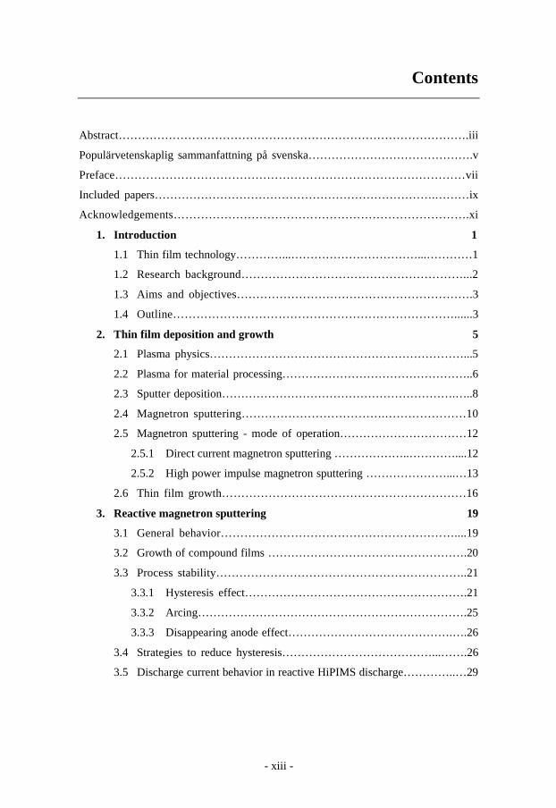
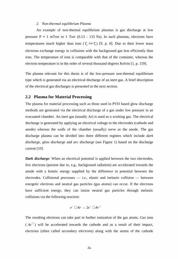
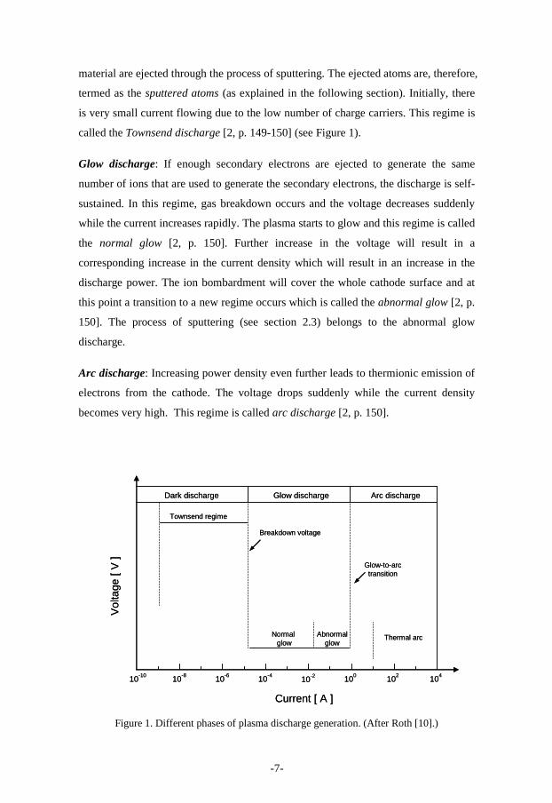
discharge plasma can be divided into three different regimes which include dark
discharge, glow discharge and arc discharge (see Figure 1) based on the discharge
current [10].
Dark discharge: When an electrical potential is applied between the two electrodes,
few electrons (present due to, e.g., background radiation) are accelerated towards the
anode with a kinetic energy supplied by the difference in potential between the
electrodes. Collisional processes — i.e., elastic and inelastic collision — between
energetic electrons and neutral gas particles (gas atoms) can occur. If the electrons
have sufficient energy, they can ionize neutral gas particles through inelastic
collisions via the following reaction:
+−− +→+ AreAre 2
The resulting electrons can take part in further ionization of the gas atoms. Gas ions
( +Ar ) will be accelerated towards the cathode and as a result of their impact,
electrons (often called secondary electrons) along with the atoms of the cathode
-6-
- 7 -
material are ejected through the process of sputtering. The ejected atoms are, therefore,
termed as the sputtered atoms (as explained in the following section). Initially, there
is very small current flowing due to the low number of charge carriers. This regime is
called the Townsend discharge [2, p. 149-150] (see Figure 1).
Glow discharge: If enough secondary electrons are ejected to generate the same
number of ions that are used to generate the secondary electrons, the discharge is self-
sustained. In this regime, gas breakdown occurs and the voltage decreases suddenly
while the current increases rapidly. The plasma starts to glow and this regime is called
the normal glow [2, p. 150]. Further increase in the voltage will result in a
corresponding increase in the current density which will result in an increase in the
discharge power. The ion bombardment will cover the whole cathode surface and at
this point a transition to a new regime occurs which is called the abnormal glow [2, p.
150]. The process of sputtering (see section 2.3) belongs to the abnormal glow
discharge.
Arc discharge: Increasing power density even further leads to thermionic emission of
electrons from the cathode. The voltage drops suddenly while the current density
becomes very high. This regime is called arc discharge [2, p. 150].
Figure 1. Different phases of plasma discharge generation. (After Roth [10].)
10-10 10-8 10-6 10-410-2 100 102 104
Current [ A ]
Vol
tage
[ V
]
Dark discharge Glow discharge Arc discharge
Townsend regime
Breakdown voltage
Normal glow
Abnormalglow
Thermal arc
Glow-to-arctransition
10-10 10-8 10-6 10-410-2 100 102 104
Current [ A ]
Vol
tage
[ V
]
Dark discharge Glow discharge Arc discharge
Townsend regime
Breakdown voltage
Normal glow
Abnormalglow
Thermal arc
Glow-to-arctransition
-7-
- 8 -
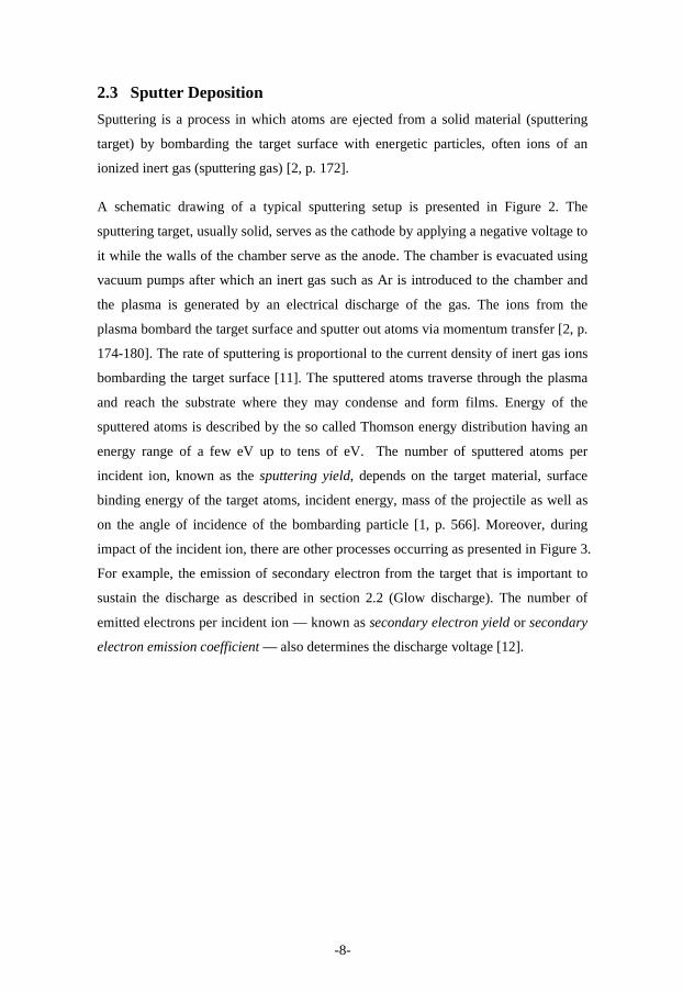
2.3 Sputter Deposition
Sputtering is a process in which atoms are ejected from a solid material (sputtering
target) by bombarding the target surface with energetic particles, often ions of an
ionized inert gas (sputtering gas) [2, p. 172].
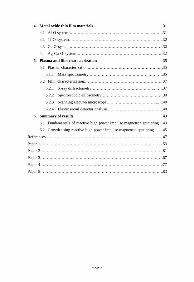
A schematic drawing of a typical sputtering setup is presented in Figure 2. The
sputtering target, usually solid, serves as the cathode by applying a negative voltage to
it while the walls of the chamber serve as the anode. The chamber is evacuated using
vacuum pumps after which an inert gas such as Ar is introduced to the chamber and
the plasma is generated by an electrical discharge of the gas. The ions from the
plasma bombard the target surface and sputter out atoms via momentum transfer [2, p.
174-180]. The rate of sputtering is proportional to the current density of inert gas ions
bombarding the target surface [11]. The sputtered atoms traverse through the plasma
and reach the substrate where they may condense and form films. Energy of the
sputtered atoms is described by the so called Thomson energy distribution having an
energy range of a few eV up to tens of eV. The number of sputtered atoms per
incident ion, known as the sputtering yield, depends on the target material, surface
binding energy of the target atoms, incident energy, mass of the projectile as well as
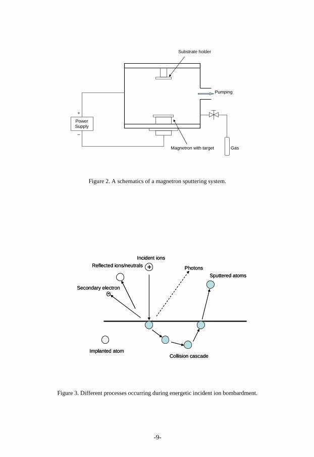
on the angle of incidence of the bombarding particle [1, p. 566]. Moreover, during
impact of the incident ion, there are other processes occurring as presented in Figure 3.
For example, the emission of secondary electron from the target that is important to
sustain the discharge as described in section 2.2 (Glow discharge). The number of
emitted electrons per incident ion — known as secondary electron yield or secondary
electron emission coefficient — also determines the discharge voltage [12].
-8-
- 9 -
Figure 2. A schematics of a magnetron sputtering system.
Figure 3. Different processes occurring during energetic incident ion bombardment.
Power Supply
Gas
Pumping
+
_
Magnetron with target
Substrate holder
+
Collision cascadeImplanted atom
Sputtered atoms
Incident ions
Reflected ions/neutrals
Secondary electron
Photons
-
+
Collision cascadeImplanted atom
Sputtered atoms
Incident ions
Reflected ions/neutrals
Secondary electron
Photons
--
-9-
- 10 -
2.4 Magnetron Sputtering
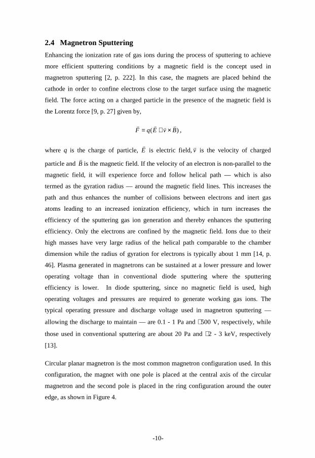
Enhancing the ionization rate of gas ions during the process of sputtering to achieve
more efficient sputtering conditions by a magnetic field is the concept used in
magnetron sputtering [2, p. 222]. In this case, the magnets are placed behind the
cathode in order to confine electrons close to the target surface using the magnetic
field. The force acting on a charged particle in the presence of the magnetic field is
the Lorentz force [9, p. 27] given by,
)( BvEqFvvvv
×+= ,
where q is the charge of particle, Ev
is electric field,vv
is the velocity of charged
particle and Bv
is the magnetic field. If the velocity of an electron is non-parallel to the
magnetic field, it will experience force and follow helical path — which is also
termed as the gyration radius — around the magnetic field lines. This increases the
path and thus enhances the number of collisions between electrons and inert gas
atoms leading to an increased ionization efficiency, which in turn increases the
efficiency of the sputtering gas ion generation and thereby enhances the sputtering
efficiency. Only the electrons are confined by the magnetic field. Ions due to their
high masses have very large radius of the helical path comparable to the chamber
dimension while the radius of gyration for electrons is typically about 1 mm [14, p.
46]. Plasma generated in magnetrons can be sustained at a lower pressure and lower
operating voltage than in conventional diode sputtering where the sputtering
efficiency is lower. In diode sputtering, since no magnetic field is used, high
operating voltages and pressures are required to generate working gas ions. The
typical operating pressure and discharge voltage used in magnetron sputtering —
allowing the discharge to maintain — are 0.1 - 1 Pa and ∼500 V, respectively, while
those used in conventional sputtering are about 20 Pa and ∼2 - 3 keV, respectively
[13].
Circular planar magnetron is the most common magnetron configuration used. In this
configuration, the magnet with one pole is placed at the central axis of the circular
magnetron and the second pole is placed in the ring configuration around the outer
edge, as shown in Figure 4.
-10-
- 11 -
(a)
(b)
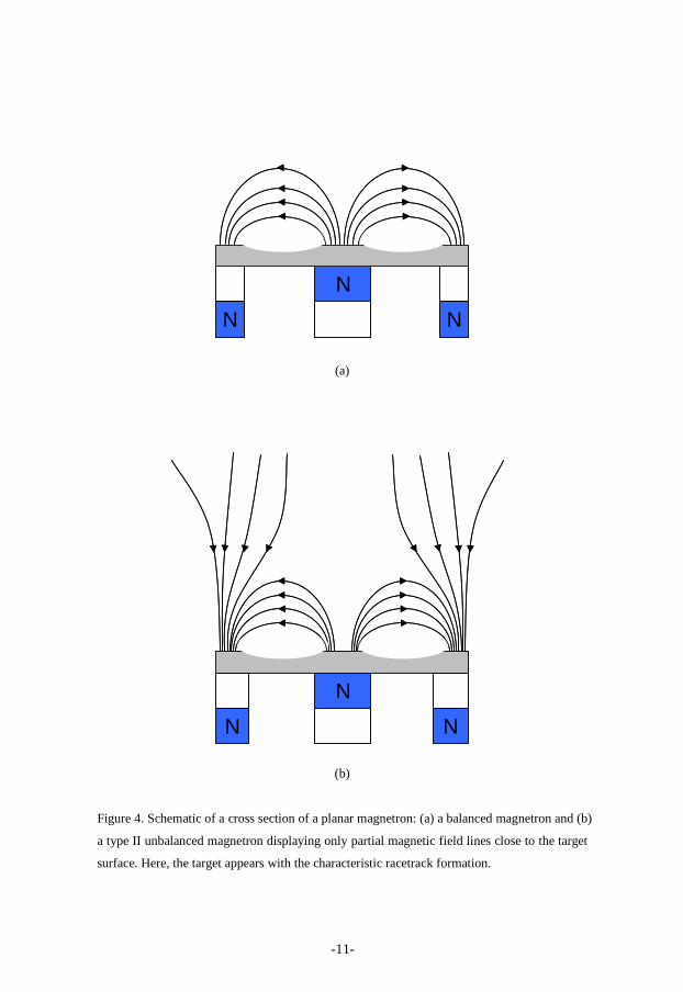
Figure 4. Schematic of a cross section of a planar magnetron: (a) a balanced magnetron and (b)
a type II unbalanced magnetron displaying only partial magnetic field lines close to the target
surface. Here, the target appears with the characteristic racetrack formation.
N N
N
N N
N
N N
N
N N
N
-11-
- 12 -
In general, there are two standard types of magnetic field configuration used in
deposition by magnetron sputtering [13]:
Balanced magnetron
The inner and outer magnets have the same strength which confines the electrons
close to the target surface. This means that the plasma does not reach to the substrate
and results in low ion bombardment of the substrate (ion current density < 1 mAcm-2)
during film growth, thereby leading to low mobility of the depositing atoms on the
substrate. This configuration is displayed in Figure 4 (a).
Unbalanced magnetron
If the inner magnet has a stronger pole than the outer magnet, the magnetic field
configuration is unbalanced (type I unbalanced magnetron). In the type II
configuration, the inner pole is weaker than the outer pole; the magnetic field lines
open up and extend towards the substrate (see Figure 4 (b)). The electrons follow the
field lines and, therefore, the plasma is also extended to the substrate. Ion
bombardment (ion current density = 2 - 10 mAcm-2) during growth can beneficially
influence the film properties, such as increase coatings density and improve adhesion
to the substrate.
2.5 Magnetron Sputtering - Modes of Operation
There are variants of magnetron sputtering depending on how the power is applied.
Among these, the techniques used in this thesis are direct current magnetron
sputtering and high power impulse magnetron sputtering.
2.5.1 Direct Current Magnetron Sputtering
In thin film sputtering deposition, direct current magnetron sputtering (DCMS) is
successfully used to grow conducting thin films at high deposition rates whereas it
can also be scaled for making large scale deposition of thin films. This makes DCMS
an industrially attractive deposition technique. In DCMS, a constant power is applied
to the target which is limited by the thermal load on the target. This power limitation
(maximum power densities of a few 10s of Wcm-2) does not allow for generating high
plasma densities and the resulting ion fraction of the sputtered material is very low
(only a few percent for metals) [15]. The majority of the flux is therefore consisting of
neutral depositing species with energy of few eV. Overall, this results in the energy of
-12-
- 13 -
the sputtered species limiting the energy input into the substrate. It is possible to
improve the film quality by applying a negative potential to the substrate, additional
heat at the substrate and using an unbalanced magnetron (type II). This will provide
the possibility of ion bombardment during film growth thereby improving the film
quality.
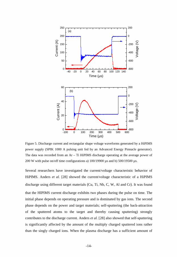
2.5.2 High Power Impulse Magnetron Sputtering
A high power impulse magnetron sputtering (HiPIMS) discharge is operated with
very high instantaneous power which facilitates the generation of high plasma
densities, thereby creating highly ionized depositing fluxes. This scheme was
introduced by Kouznetsov et al. [16] in 1999. In HiPIMS, the power to the cathode is
applied using short uni-polar pulses of low duty cycle (pulse on-time divided by the
period of the pulse) resulting in very high target peak power densities of the order of
kWcm-2 [15–17]. The typical discharge current and voltage waveforms in HiPIMS are
shown in Figure 5 (a).
Thanks to the high peak power, dense plasma is generated in front of the target with
typical plasma densities in the order of 1019 m-3. High electron density facilitates
ionization of neutral species and a high degree of ionization of both gas and sputtered
species is reached [16]. Ionized depositing fluxes provide the possibility to control
their energy and direction during film growth [18,19]. The energetic bombardment
during the film growth facilitates the growth of films with superior properties as
compared to those obtained by conventional magnetron sputtering techniques, e.g.,
denser films [20–22], tailored film structures [15,21,23,24], good mechanical [22,24–
26] and electrical [27] properties, etc.
-13-
- 14 -
-40 -20 0 20 40 60 80 100 120 1400
50
100
150
200
250
Vol
tage
(V
)
Cur
rent
(A
)
Time (µs)
(a)
-800
-600
-400
-200
0
200
-100 0 100 200 300 400 500 6000
20
40
60
Vol
tage
(V
)
Cur
rent
(A
)
Time (µs)
-800
-600
-400
-200
0
200
(b)
Figure 5. Discharge current and rectangular shape voltage waveforms generated by a HiPIMS
power supply (SPIK 1000 A pulsing unit fed by an Advanced Energy Pinnacle generator).
The data was recorded from an Ar – Ti HiPIMS discharge operating at the average power of
200 W with pulse on/off time configurations a) 100/19900 µs and b) 500/19500 µs.
Several researchers have investigated the current/voltage characteristic behavior of
HiPIMS. Anders et al. [28] showed the current/voltage characteristic of a HiPIMS
discharge using different target materials (Cu, Ti, Nb, C, W, Al and Cr). It was found
that the HIPIMS current discharge exhibits two phases during the pulse on time. The
initial phase depends on operating pressure and is dominated by gas ions. The second
phase depends on the power and target materials; self-sputtering (the back-attraction
of the sputtered atoms to the target and thereby causing sputtering) strongly
contributes to the discharge current. Anders et al. [28] also showed that self-sputtering
is significantly affected by the amount of the multiply charged sputtered ions rather
than the singly charged ions. When the plasma discharge has a sufficient amount of
-14-
- 15 -
multiply charged ions of the sputtered material, these ions can be back attracted to the
target giving rise to secondary electron emission which subsequently results in the
transition of the discharge to the high current regime (see for example Figure 11 in
[28]).
Besides bombardment of the target with the highly energetic positive gas ions, the
kinetic energy from the ions transferred to the target also results in heat generated at
the target surface. This heat can be transferred to the gas in front of the target. If we
assume that the process gas obeys the ideal gas law, then the pressure of the gas (Pgas)
can be given as,
Pgas = ngaskT ,
where k is the Boltzmann constant, ngas is the gas density and T is the gas temperature.
In the case that the gas pressure in the chamber is constant (Isobaric process),
increased gas temperature leads to lower gas density (gas dilution effect or gas
rarefaction effect) [29]. Moreover, the sputtered atoms also transfer energy to the gas
atoms in front of the target via momentum transfer which means the gas density in
front of the target surface is low which adds to the gas rarefaction. This phenomenon
is also referred to as sputtering wind [30]. The magnitude of the gas rarefaction
depends on several parameters [31], e.g., applied power, gas pressure and gas species.
With HiPIMS plasma conditions — where the ionized particle density is very large —
the effect of gas rarefaction is enhanced. Several researchers have investigated this
phenomenon for HiPIMS as well as for Ionized PVD processes [17,28,29,31,32]. The
decreased gas density in front of the target due to gas rarefaction results in the
decrease of the sputtering gas ions which in turn causes a decrease in the discharge
current [33] (see Figure 5 (b)). The effect of gas rarefaction and behavior of the
discharge current for Ti and Al during the growth of Ti-O and Al-O have been
discussed in Paper 4.
There are some disadvantages with HiPIMS, e.g. a lower deposition rate for metals as
compared to conventional magnetron sputtering at the same average power.
Helmersson et al. [15] reviewed deposition rate data in HiPIMS and found that the
rates are typically 25 - 35% of the rates in DCMS. This observed low deposition rate
can be attributed to several mechanisms, such as back-attraction of metal ions to the
-15-
- 16 -
target followed by self-sputtering [15,34,35] and anomalous transport of the sputtered
species [36]. However, it is possible to increase the deposition rate by optimizing the
parameters such as changing the magnetic field of the magnetron [37], applying a
magnetic coil between the substrate and magnetron target [19].
2.6 Thin Film Growth
In the process of a film formation, atoms such as those sputtered from a target — in
the case of magnetron sputtering — reach the substrate and condense to form a
coating. There are several parameters that influence the growth behavior and
structural features of thin films. These parameters are determined by the deposition
conditions and influence how the atoms behave at the substrate before they are fully
bonded to form films (refered to as adatoms) as well as the kinetics of the atoms (such
as mobility, diffusion) at the substrate surface. The dependence of the structural
features of thin films on the deposition conditions are often illustrated in the form of
structure-zone diagrams, also known as structure zoned models (SZMs) [2, p. 497].
The first structure zone model for magnetron-sputtered metal thin films was proposed
by Thornton [38]. The parameters that are used for describing the microstructural
evolution of the films in this model are sputtering gas pressure and substrate
temperature.
Sputtering gas pressure: Higher pressure means more frequent collisions of the
sputtered atoms with the background gas and loss of energy. Therefore, the energy of
the atoms arriving to the substrate is lower resulting in low adatom mobility giving
films with a porous microstructure at low substrate temperature.
Substrate temperature: This represents the thermal effect on the film growth. Higher
temperature of the substrate can enhance adatom mobility/diffusion which allows
particles to find energetically favorable positions, resulting in formation of a film with
larger grains (often columnar). At low temperature, the mobility/diffusion of adatom
is very low, resulting in films with smaller grains or disordered structure. Low
temperature films also contain more voids.
The SZM presented by Thornton is divided into four zones (1, T, 2 and 3) based on
the resulting microstructure of the films influenced by the sputtering gas pressure and
substrate temperature (in the SZM, the ratio of the substrate temperature and melting
-16-
- 17 -
point of the source material, i.e. Ts/Tm, has been used). The SZM is briefly discussed
here:
1. Zone 1.
The structure of the films appear amorphous or of poor crystalline structure
(many defects). The size of columns is typically tens of nanometers in diameter and
the individual columns are separated by voided boundaries due to limited diffusion of
adatoms on the surface. This zone occurs when the ratio Ts/Tm is in the range 0.1 - 0.5
and sputtering gas pressure is in the range 0.15 - 4 Pa.
2. Zone T.
Films in this zone contain poor crystalline structure similar to zone 1 but with
no voids present. This zone may be considered as a transition between zones 1 and 2.
The ratio Ts/Tm is in the range of 0.1 - 0.4 at sputtering gas pressure 0.15 Pa, and Ts/Tm
is in the range 0.4 - 0.5 at sputtering gas pressure 4 Pa.
3. Zone 2.
In this zone crystalline columnar grain with fewer defects than in zone 1 are
found. There are no voids (dense grain boundaries) between the columns. Ts/Tm is in
the range 0.4 - 0.7 and atoms have energy high enough to diffuse on the surface.
4. Zone 3.
This zone occurs at Ts/Tm > 0.6, which is high enough to activate bulk
diffusion in the film.
In addition, there are other parameters such as sputtering power, substrate bias, and
deposition rate that influence the microstructure of films. However, the microstructure
still falls within one of the SZMs proposed by Thornton and is determined by the
energy of adatoms.
-17-

- 18 -
-18-
- 19 -
Chapter 3
Reactive Magnetron Sputtering
In this chapter, the fundamentals of a reactive magnetron sputtering process along
with the discussion on elimination/suppression of the hysteresis effect are described.
3.1 General Behavior
Compound films such as metal oxides or metal nitrides are commonly deposited using
an insulating compound target via radio frequency (RF) magnetron sputtering [2, p.
211]. However, the deposition rate is low because of the lower sputtering yield of the
compound material relative to metal, especially in metal oxide. Also the sputtering
efficiency in RF discharges is low. Another limitation of RF sputtering is its
complicated and expensive hardware [3]. Therefore, RF magnetron sputtering is less
attractive for industrial processes.
Reactive DC magnetron sputtering is an alternative technique for compound film
deposition with potentially higher deposition rates than RF magnetron sputtering.
Also, it uses metal targets which are easier and cheaper to manufacture. In a typical
DCMS reactive process, compound film is synthesized in the presence of a reactive
gas mixed with an inert working gas (e.g., Ar) by sputtering of a metallic target [2, p.
216]. Reactive gas in the discharge will react and form the desired compound at the
substrate. For example, in the case of Al2O3 film growth, oxygen is introduced and
-19-
- 20 -
reacts with sputtered Al species to form Al2O3 on the substrate. In practice, however,
there are some challenges which have to be addressed. Due to the process instability
during reactive sputtering deposition, the deposition rates may be low. Also, the film
stoichiometry may be influenced by the process conditions.
3.2 Growth of Compound Films
In reactive sputtering the sputtered material reacts with the reactive gas species and
forms a compound. This offers the possibility to control the chemical composition and
other film properties by varying the ratio between fluxes of the sputtered material and
reactive gas.
For a typical reactive sputtering process, three different modes — metal mode,
compound mode and the transition between them — are usually considered based on
the reactive gas flow rate [4]. These modes are briefly discussed below.
1. Metal mode.
In this mode, the reactive gas flow fed into the chamber is not sufficient
(reactive gas partial pressure is low) to react with all the sputtered material deposited
at the surfaces in the chamber such as chamber walls, substrate and target. Thereby,
the deposited film at the substrate is sub-stoichiometric and the desired properties of
the film are not achieved due to the excess of target material (e.g. the composition
corresponds to SiO2-x, TiO2-x or TiN1-x). The sputtering target surface in this mode is
predominantly metallic with a low fraction of compound.
2. Transition mode.
In this region, there is a complex dependence of the composition on the
reactive gas flow typically there is more than one working point corresponding to a
single value of the gas flow. Depending on the working point, the deposited films may
be stoichiometric while the target surface is still metallic. The optimum working point,
however, may be unstable.
3. Compound mode.
If the amount of the reactive gas is further increased the reactive gas partial
pressure will be high and the whole target surface will be covered by the compound
film (completely poisoned). This mode is referred to as compound mode. In this
-20-
- 21 -
region, the sputtering efficiency decreases which results in lower deposition rate as
compared to the transition mode. This is a result of low sputtering yield of most
compounds, especially oxides. In some cases, compound mode is preferred because of
its stability, such as in large area coatings on glass. In addition to the low deposition
rate, excess of reactive gas may result in over-stoichiometric composition of some
compounds such as TiN with undesirable color.
3.3 Process Stability
During a reactive sputtering process, the reaction between the target material and the
reactive gas might lead to process instability due to several effects [4]. The most
common among these are: (1) Hysteresis (2) Arcing and (3) Disappearing anode.
3.3.1 Hysteresis Effect
The hysteresis effect is an issue to overcome in reactive sputtering in order to deposit
stoichiometric films at a high deposition rate. If the discharge power is kept constant
and the reactive gas flow is increasing, there will be a critical point in the reactive gas
flow where the transition to compound mode occurs. At this critical point, the
compound formation takes place at the whole surface of the sputtering target resulting
in a sudden change in the sputtering rate as compared to the metal surface. Thereby,
the deposition rate suddenly decreases. This is accompanied by an increase of reactive
gas partial pressure. Typically, the sputtering yield of the compound is substantially
lower than that of the elemental material [3–5]. This causes the deposition rate to
decrease as the supply of the reactive gas increases which leads to a further decrease
in the deposition rate and an avalanche like transition from metal to compound mode
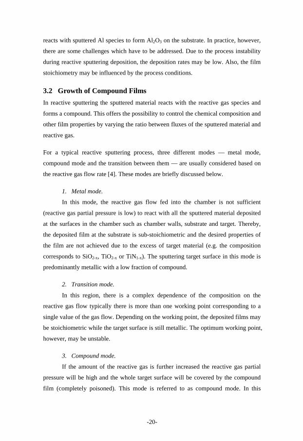
of operation. A typical experimental processing curve for the mass deposition rate vs.
the supply of the reactive gas is shown in Figure 6. The mass deposition rate drops
when the reactive gas flow is higher than the critical reactive gas flow. However,
when decreasing the reactive gas flow the deposition rate does not increase at the
same point but needs to be reduced more to show hysteresis in the gas flow [3–5]. The
resulting curve is referred to as a hysteresis curve. The area between the decreasing
and increasing points is referred to as the hysteresis region, sometimes also called
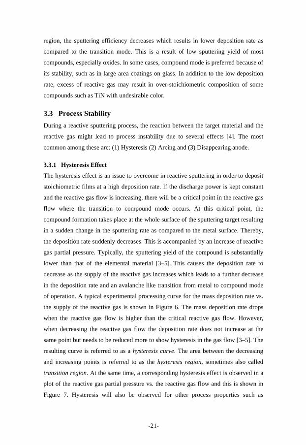
transition region. At the same time, a corresponding hysteresis effect is observed in a
plot of the reactive gas partial pressure vs. the reactive gas flow and this is shown in
Figure 7. Hysteresis will also be observed for other process properties such as
-21-
- 22 -
discharge voltage and discharge current. This is because secondary electron yield also
changes when the compound mode started which also affects the plasma impedance.
The change of discharge voltage or discharge current (decrease or increase) as
compared to the discharge voltage or discharge current in metal mode depends on the
target material [12].
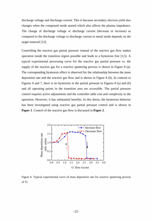
Controlling the reactive gas partial pressure instead of the reactive gas flow makes
operation inside the transition region possible and leads to a hysteresis free [3,5]. A
typical experimental processing curve for the reactive gas partial pressure vs. the
supply of the reactive gas for a reactive sputtering process is shown in Figure 8 (a).
The corresponding hysteresis effect is observed for the relationship between the mass
deposition rate and the reactive gas flow and is shown in Figure 8 (b). In contrast to
Figures 6 and 7, there is no hysteresis in the partial pressure in Figures 8 (a) and (b)
and all operating points in the transition area are accessible. The partial pressure
control requires active adjustments and the controller adds cost and complexity to the
operation. However, it has substantial benefits. In this thesis, the hysteresis behavior
has been investigated using reactive gas partial pressure control and is shown in
Paper 1. Control of the reactive gas flow is discussed in Paper 2.
0.0 0.5 1.0 1.5 2.0 2.5 3.0 3.5 4.00.0
0.5
1.0
1.5
2.0
O2 flow (sccm)
Mas
s de
posi
tion
rate
(a
rb.
units
)
Increase flow Decrease flow
Figure 6. Typical experimental curve of mass deposition rate for reactive sputtering process
of Ti.
-22-
- 23 -
0
20
40
60
80
100
120
140
0.0 0.5 1.0 1.5 2.0 2.5 3.0 3.5 4.0
O2 p
artia
l pre
ssur
e (m
Pa)
Increase flow
O2 flow (sccm)
Decrease flow
Figure 7. The partial pressure, P, of the reactive gas corresponding to the curve in Figure 6.
0
20
40
60
80
100
0.0 0.2 0.4 0.6 0.8 1.00.0
0.2
0.4
7
6
6
5
4
2
2
1
O2
part
ial p
ress
ure
(mP
a)
1
(a)
(b)
7
5
4
3
3
Mas
s de
posi
tion
rate
(a
rb.
units
)
O2 flow (sccm)
Figure 8. Diagram illustrating the process operates by controlling the O2 partial pressure for
the reactive sputtering of Al-O. (a) shows the general behavior for the O2 partial pressure vs.
O2 gas flow and (b) shows mass deposition rate vs. O2 gas flow. The example numbers
indicated by 1, 2, …, 7 in (a) correspond to points 1, 2, …, 7 in (b)
-23-
- 24 -
As mentioned above, the sputtering yield of oxides is typically lower than that of
metals, which means that sputtering from an oxide target results in lower deposition
rates as compared to that of the metal mode. Large scale industrial processes require
that films are grown at high deposition rates with a stable process. Higher deposition
rates can be obtained by sputtering at a suitable point in the transition mode, thereby
avoiding a fully poisoned target — using a process control based on a suitable
feedback signal control to control the gas flow in order to keep the process stable.
There are several quantities in reactive sputtering which can be used as a feedback
signal for process control. Some types of signals are described in literature reviews
[3,4] and references therein:
1. Optical emission spectrometer (OES) signal
When the partial pressure of the reactive gas increases, then the intensity of
emission lines from the sputtered material decreases. This is due to an increasing
fraction of the target surface covered by compound material which leads to a lower
erosion rate. Schiller et al. [39] used the optical emission line of the target material as
a feedback signal by adjusting the gas flow and were able to control the constant
partial pressure of reactive gas during the deposition.
2. Mass spectrometer signal
Mass spectrometry measures the mass-to-charge ratio of charged particles and
thus can analyze the chemical composition of the process atmosphere. Therefore, this
technique provides a direct measure of the partial pressures (more details of mass
spectrometry will be described in Chapter 5, section 5.1.1). Sproul and Tomashek [3]
used mass spectrometry in order to maintain a constant partial pressure during the
deposition. One issue with the mass spectrometer is that there is drift in signal
intensity with time; however the ratio of peaks remains relatively constant with time,
which can be used to compensate for this drift.
3. Cathode voltage signal
If the power (or current) is kept constant while changing the reactive gas flow,
then the discharge voltage changes due to the change of the secondary electron yield
of the target thus affecting the plasma impedance. Affinito and Parsons [40] used the
feedback signal from the cathode voltage to stabilize the transition zone during
deposition. However, this signal is not sensitive only to the partial pressure of reactive
-24-
- 25 -
gas but also to other parameters such as target thickness and temperature of the target
that influence the cathode voltage. Therefore, using this feedback to synthesize a true
stoichiometric film is difficult.
4. Oxygen sensor
An oxygen sensor is an electronic device which detects the concentration of
oxygen. Typical oxygen sensor includes two porous electrodes, commonly platinum
separated by a ceramic electrolyte such as yttria stabilized zirconia (YSZ) and
semiconducting metal oxide (TiO2, CeO2, etc). One electrode is in contact with the
ambient and the other in contact with the test gas environment. The oxygen molecules
are adsorbed by electrode and dissociate into atomic oxygen. The electrons from
electrolyte can transfer to oxygen atoms forming oxygen ions. The oxygen ions are
collected by the electrodes creating a voltage difference between them. Such a sensor
is used in various fields such as medical, food processing and automobiles [41]. The
main use of oxygen sensors is in automobile engines in order to control the air-fuel
ratio (Lambda, λ) in the combustion engine. This oxygen sensor is also referred to as
Lambda probe [41]. Thereby, the oxygen sensor output is fed back to the engine
control for controlling the engine operates around the stoichiometric point (λ = 1). In
Paper 1, we used a lambda probe to detect the amount of oxygen introduced into the
chamber. The potential measured by the lambda probe is send to the control unit and
used to control oxygen gas mass flow controller in order to maintain the oxygen
partial pressure. The advantage of using a lambda probe is the size and price, which
makes it suitable for large area coating control systems with multiple sensors.
3.3.2 Arcing
In reactive sputtering of insulating films, arcing occurs on the target surface in the
regions covered by non-conductive coatings. Positive charges will be collected at the
non-conductive layer due to bombardment by positively charged ions. This charge can
build up until the charge reaches the breakdown voltage and an arc will occur. There
are many techniques, including RF power supply, a rotated cylindrical target [3,4],
which are employed to avoid arcing. One commonly employed method of avoiding or
significantly reducing the arcing effect during film deposition is to use pulsed DC
reactive sputtering [42]. With this technique, an asymmetric bipolar pulsed voltage
(the positive level is about only 10% of the negative peak level) is applied to the
-25-
- 26 -
cathode in order to allow for electrons to be attracted to the target surface to discharge
the non-conductive layer.
3.3.3 Disappearing Anode Effect
Another commonly encountered problem in a reactive deposition process of insulating
films is that insulating layers are also formed on the chamber walls (i.e., the walls
serve as the anode for the discharge). This means the anode will gradually lose the
ability to collect electrons, resulting in a shift of the plasma potential to a situation
where the potential between the cathode and the plasma disappears and the plasma is
extinguished. There are various methods to avoid the disappearing anode effect, for
example, using dual magnetron sputtering [3,4].
3.4 Strategies to Reduce Hysteresis
In this thesis, we focus on the problem of hysteresis. Elimination or suppression of
hysteresis could enable high rate sputtering without a feedback control unit which
would be very beneficial. Berg and Nyberg [5] studied the parameters which
influence the hysteresis effect by proposing a model for reactive sputtering. They
discussed the dependence of the hysteresis on the gas pressure, deposition rate as well
as reactive gas flow. The model also presented various ways to reduce or remove the
hysteresis. Most of them, however, have limitations which prevent industrial use.
The examples of methods to reduce hysteresis in reactive sputtering are briefly
summarized here:
1. Increasing pumping speed
Pumping speed is an important parameter that affects the hysteresis. Kadlec et
al. [43] showed that if the pumping speed of the system (Sp) is greater than the critical
pumping speed, the hysteresis effect can be avoided. In the model by Berg and
Nyberg [5], it was shown that when the derivative of the total supply (sum of all
sources for reactive gas consumption (Qtot) and pressure (P) is higher than
zero
> 0dP
dQtot , the hysteresis can be eliminated. However, the drawback of this
method is the requirement for a very high pumping speed, especially for a large
deposition system. For these reasons, the high pumping speed approach is not used
very often.
-26-
- 27 -
2. Reduction of the target area
The area of the sputtering target also influences the hysteresis effect. Berg and
Nyberg [5] showed that reducing the target area can reduce the width of hysteresis
loop. Nyberg et al. [44] also showed corresponding experimental results. The problem
of this method is the film uniformity which complicates deposition on large area
substrates. However, they demonstrated that moving magnets inside the target
assembly may be used.
3. Sub-stoichiometric target
Kubart et al. [45] have shown that the hysteresis effect can be removed by
targets consisting of a mixture of compound and metal material (i.e., a fraction of
composition between TiO2 and Ti powders). They also shown a high deposition rate
can be achieved when the target composition is optimized.
4. Gas composition
Severin et al. [46] suggested that for some metal oxide systems the addition of
nitrogen gas into the sputtering atmosphere during reactive sputtering leads to
stabilization of the process and the hysteresis effect can be eliminated. This is due to
the higher sputtering yield of nitride than the sputtering yield of oxide. However, the
deposited films contained low amounts of nitrogen.
5. Reactive HiPIMS
Initially, HiPIMS was used in reactive sputtering of metal nitrides for wear
and corrosion resistant coatings (hard coating) as well as decorative coatings — e.g.,
CrNx [22], TiNx [47], etc. The deposited films show superior properties such as
excellent adhesion, denser structure and higher hardness than films deposited by
conventional PVD. In reactive HiPIMS of metal oxides, there are also improved film
properties as compared to films deposited by conventional magnetron sputtering, e.g.,
films with a high refractive index [48,49], higher film density [48,50] and higher
crystalline at lower deposition substrate temperature growth [51]. Achieving higher
deposition rates in reactive HiPIMS vs. reactive DCMS is in contrast to results found
in non-reactive sputtering (as previously discussed in section 2.5). This is due to the
possibility to increase process stability during reactive deposition by HiPIMS [6,7].
However, the understanding of the mechanisms involved during reactive processes
-27-
- 28 -
using HiPIMS remains very limited. A brief review of the studies performed on the
process stability when using reactive HiPIMS is presented below.
HiPIMS facilitates the elimination/suppression of the hysteresis. The first report on
the hysteresis effect using HiPIMS and conventional DCMS on the Al-O system was
presented by Wallin and Helmersson [6]. The work showed that HiPIMS can
eliminate the hysteresis. The results demonstrated stabilization of the transition zone
leading to true stoichiometric films with a high deposition rate. The authors suggested
that the observed behavior is due to a high erosion rate during the pulses which can
remove the compound film on the target surface. Furthermore, it might be an effect of
limited target oxidation between the pulses and hence reduced target poisoning.
Another study of hysteresis in HiPIMS was published by Sarakinos et al. [7]. Zr-O
system was used to investigate the hysteresis effect during reactive HiPIMS and
DCMS. In that work the off-time was varied keeping the pulse on-time constant at 50
µs (off-time 450 µs and 1450 µs, corresponding with pulse frequency 2 kHz and ∼666
Hz, respectively). The results showed that HiPIMS led to stabilization of the transition
zone and also the deposition rate was higher than DCMS. The explanation was based
on a high erosion rate of the compound film during the pulses. This is because of a
higher discharge voltage in HiPIMS compared to DCMS resulting in higher sputtering
yield. In general, HiPIMS uses higher discharge voltage to maintain the plasma than
in DCMS and a longer off-time (lower frequency) needs a higher discharge voltage.
They calculated sputtering yield of ZrO2 based on the observed discharge voltage and
found that a higher sputtering yield of compound films on the target surface during
the pulse on-time when the pulse off-time is longer. These two studies confirmed that
HiPIMS can eliminate/suppress the hysteresis effect and made the process more stable
than DCMS.
Recently, Audronis et al. [52] reported characteristics of the hysteresis effect using
HiPIMS as well as DCMS for the Ti-O system. The results show no difference in
hysteresis width between HiPIMS and DCMS; also, pulse frequency and duty cycle
only affect the overall shape of the hysteresis effect. This has been attributed to the
pronounced reactive ion implantation to the target surface in reactive HiPIMS due to
very high peak voltage (which leads to stronger target poisoning). It should be noted
that — in contrast to Wallin and Helmersson [6] and Sarakinos et al. [7] — Audronis
-28-
- 29 -
et al. [52] used low frequencies (300, 450 and 600 Hz; the pulse on-time was 50 µs)
and a very large target area (188 mm × 296 mm × 9.5 mm). The material system was
also different from Wallin and Helmersson [6] and Sarakinos et al. [7]. It should also
be noted that, the measurements by Audronis et al. were very fast. They could record
the whole hysteresis curve in only a few minutes.
At the moment, there are several explanations of the hysteresis behavior in reactive
HiPIMS. We would like to focus more on this phenomenon. In Paper 1 and Paper 2,
we study the possibility of stabilizing the transition zone by reactive HiPIMS over a
wide range of experimental parameters such as pulse frequency and duty cycle, etc.
We also investigate the effect of target materials, pumping speed, target area, etc.,
which influences the hysteresis effect. In addition, we seek to contribute to the
understanding of the fundamental mechanisms that determine the process
characteristics in reactive HiPIMS processes.
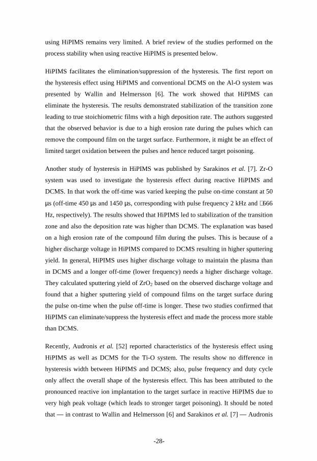
3.5 Discharge Current Behavior in a Reactive HiPIMS Discharge
As described in section 2.5.2 — i.e., the discharge behavior in metal mode of HiPIMS
— we found that the discharge current in a reactive HiPIMS process (using oxygen as
the reactive gas) shows a pronounced difference in shape and peak value as compared
to the metal mode. The discharge current waveforms in the metal (Ar) and oxide
mode of HiPIMS (Ar+O2) for (a) Ti and (b) Al sputtering targets are shown in Figure
9. It is very surprising that both Ti and Al show the same discharge current behavior
in oxide mode as compared to their metal mode. This is because the change in the
secondary electron yield of Ti and Al in oxide mode is different. In general, the
secondary electron yield of Ti is lower in oxide mode as compared to metal mode and
the opposite is true for Al [12]. In Paper 4, we investigate ion composition as well as
ion energy distribution in both metal and oxide modes for Ti and Al. The paper
contributes towards understanding the behavior.
-29-
- 30 -
-100 0 100 200 300 4000
50
100
150
200
250
300
Oxide Mode
300 W
100 W
200 W
400 W
Dis
char
ge c
urre
nt (
A)
Time (µs)
Metal Mode
400 W
300 W
200 W
100 W
(a) Ti
-100 0 100 200 300 4000
50
100
150
200
250
300
300 W
200 W
Oxide Mode
Dis
char
ge c
urre
nt (
A)
Time (µs)
Metal Mode
200 W
300 W
(b) Al
Figure 9: Typical discharge current waveforms in the metal (Ar) and oxide mode of HiPIMS
(Ar+O2) for (a) Ti and (b) Al sputtering targets. The pulsing frequency was constant (50 Hz),
the pulse length was 300 µs, and the target diameter was 100 mm. The average discharge
power was varied between 100 and 400 W.
-30-
- 31 -
Chapter 4
Metal Oxide Thin Film Materials
In this chapter, an overview of the material systems used in the thesis along with a
brief literature survey related to the synthesis of thin films using these material
systems is presented.
4.1 Al-O System
Aluminum oxide or alumina (Al2O3) is a ceramic material with excellent properties
such as high abrasive and corrosion resistance, high hardness, chemical inertness and
optical transparency [51,53–55]. However, the properties of Al2O3 strongly depend on
the structure (amorphous or crystalline), where the crystalline Al2O3 can exhibit
different phases, i.e., α, κ, θ, η, and γ [56, p. 30]. Among the different phases, α
(corundum) is the only thermodynamically stable phase. The properties make α-Al 2O3
suitable for use in cutting tools. Thin films synthesized by sputter deposition at room
temperature are typically x-ray amorphous. Metastable phases — mostly κ, θ, and γ-
Al2O3 — occur at a substrate temperature between 180–700°C in reactive magnetron
sputtering or if any special technique during the film growth, e.g., bipolar pulse dual
magnetron sputtering [54] or a RF coil is used to increase the ionization of sputtered
flux [57]. Crystalline α-Al2O3 can be synthesized by conventional pulse DCMS at
substrate temperatures approximately 760°C as demonstrated by Zywitzki et al. [53].
-31-
- 32 -
Lower substrate temperature (650°C) can be used to synthesize the α-Al 2O3 phase
using reactive HiPIMS as shown by Wallin et al. [51].
4.2 Ti-O System
Titanium dioxide or titania (TiO2) is used for various applications such as optically
transparent [58], photocatalytic [59,60] and photoelectrochemical [61] coatings. TiO2
exhibits three different phases namely anatase, rutile and brookite. The crystalline
structure for anatase and rutile is tetragonal [62], whereas brookite has an
orthorhombic structure [62]. Conventional magnetron sputtering at room temperature
produces typically x-ray amorphous films. In order to get anatase or rutile, additional
heat at the substrate during deposition is required. The anatase phase is formed at
lower temperature (∼200°C [63]) while the rutile phase is formed at higher
temperature (above 600°C [58]). Recently, anatase and rutile TiO2 thin films
deposited by reactive HiPIMS were obtained without substrate heating [64]. In Paper
4, synthesis of TiO2 thin films using reactive HiPIMS is demonstrated. The results
demonstrate the possibility of synthesis of anatase, rutile and mixed phases by
reactive HiPIMS when the peak power is varied.
4.3 Ce-O System
Cerium oxide or ceria (CeO2) is an electrical semiconductor oxide. It has a fluorite
type cubic structure [65] with a lattice constant at room temperature of 5.411 Å. CeO2
can be used for microelectronic semiconductor devices [66], chemical diffusion
barriers [67], optical coatings [68], oxygen sensors [69] and solid electrolytes for fuel
cells [70]. For thin films, many techniques are being used for fabrication of CeO2
including, thermal evaporation [71], e-beam evaporation [72], pulse laser deposition
(PLD) [73], sol-gel [74] and magnetron sputtering [70,75]. CeO2 can be deposited
directly on a silicon substrate without the need of a barrier layer due to a
crystallographic match with the substrate; the lattice mismatch parameter between
them is a very small value of 0.3% [76].
4.4 Ag-Cu-O System
Silver copper oxide, Ag2Cu2O3, was first synthesized in powder form using a co-
precipitation method and reported in 1999 by Gomez-Romero et al. [77]. Ag2Cu2O3
has a tetragonal structure with a space group I41/amd and lattice constants a =
-32-
- 33 -
0.58857 nm and c = 1.06868 nm [78]. In a theoretical study, Feng et al. [79] predicted
excellent optical and electrical properties such as a narrow band gap and a high
absorption coefficient. These properties make Ag2Cu2O3 suitable for photovoltaic
applications.
Thin films of Ag2Cu2O3 were first produced using reactive magnetron sputtering of a
copper target partially covered by silver chips [78]. However, stoichiometric
Ag2Cu2O3 films were not found. In order to synthesize the stoichiometric Ag2Cu2O3,
several researches tried to use various strategies such as co-sputtering of silver and
copper targets [80] as well as alloy targets — Ag0.9Cu0.1 [81], Ag0.8 Cu0.2 [81],
Ag0.7Cu0.3 [81], Ag0.6Cu0.4 [82] and Ag0.5Cu0.5 [83,84]. Moreover, the effect of
deposition parameters such as annealing temperature [84], deposition temperature
[81,83], oxygen flow rate [82] and deposition power [83] on the Ag2Cu2O3 films
properties was investigated. Uthanna et al. [81] and Hari et al. [85] found that the
single phase of Ag2Cu2O3 can be synthesized using an alloy silver-copper (Ag0.7Cu0.3).
Recently, Lund et al. [83] have shown that the deposition temperature in the range
200 - 300°C can be used to synthesize Ag2Cu2O3 films from an alloy silver-copper
(Ag0.5Cu0.5) target. Synthesis of Ag2Cu2O3 thin films using reactive HiPIMS is
demonstrated in Paper 5 in this thesis. The results show that the film structure
measured by grazing incidence x-ray diffraction exhibits a stoichiometry very close to
that of the bulk material which has previously not been demonstrated.
-33-

- 34 -
-34-
- 35 -
Chapter 5
Plasma and Film Characterization
In this chapter, a brief description of the analytical techniques used is given. The
techniques are divided into two groups: plasma characterization and film
characterization. The plasma characterization has been used for studying the influence
of plasma chemistry and energetic on the film properties while the film properties
such as optical, structural, etc., were investigated in order to seek a correlation
between the plasma and film properties.
5.1 Plasma Characterization
The plasma composition, ionized fluxes of the depositing species and energy
distributions of sputtered metal, reactive and sputtering gas ions were measured using
time-averaged and time-resolved mass spectrometry.
5.1.1 Mass Spectrometry
The basic operation of the mass spectrometer is described as follows. The mass
spectrometer can be divided into four sections [86]: an extractor probe, energy filter,
mass filter and detector, as shown in Figure 10.
-35-
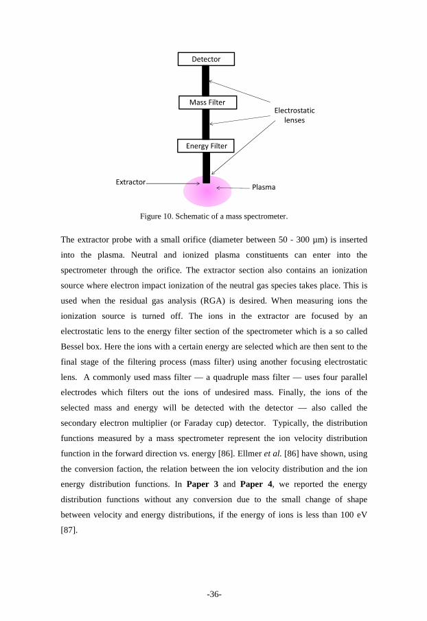
- 36 -
Detector
Mass FilterElectrostatic
lenses
Energy Filter
ExtractorPlasma
Figure 10. Schematic of a mass spectrometer.
The extractor probe with a small orifice (diameter between 50 - 300 µm) is inserted
into the plasma. Neutral and ionized plasma constituents can enter into the
spectrometer through the orifice. The extractor section also contains an ionization
source where electron impact ionization of the neutral gas species takes place. This is
used when the residual gas analysis (RGA) is desired. When measuring ions the
ionization source is turned off. The ions in the extractor are focused by an
electrostatic lens to the energy filter section of the spectrometer which is a so called
Bessel box. Here the ions with a certain energy are selected which are then sent to the
final stage of the filtering process (mass filter) using another focusing electrostatic
lens. A commonly used mass filter — a quadruple mass filter — uses four parallel
electrodes which filters out the ions of undesired mass. Finally, the ions of the
selected mass and energy will be detected with the detector — also called the
secondary electron multiplier (or Faraday cup) detector. Typically, the distribution
functions measured by a mass spectrometer represent the ion velocity distribution
function in the forward direction vs. energy [86]. Ellmer et al. [86] have shown, using
the conversion faction, the relation between the ion velocity distribution and the ion
energy distribution functions. In Paper 3 and Paper 4, we reported the energy
distribution functions without any conversion due to the small change of shape
between velocity and energy distributions, if the energy of ions is less than 100 eV
[87].
-36-
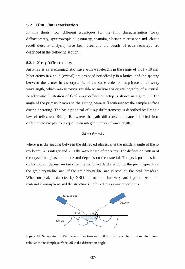
- 37 -
5.2 Film Characterization
In this thesis, four different techniques for the film characterization (x-ray
diffractometry, spectroscopic ellipsometry, scanning electron microscope and elastic
recoil detector analysis) have been used and the details of each technique are
described in the following section.
5.2.1 X-ray Diffractometry
An x-ray is an electromagnetic wave with wavelength in the range of 0.01 - 10 nm.
Most atoms in a solid (crystal) are arranged periodically in a lattice, and the spacing
between the planes in the crystal is of the same order of magnitude of an x-ray
wavelength, which makes x-rays suitable to analyze the crystallography of a crystal.
A schematic illustration of θ/2θ x-ray diffraction setup is shown in Figure 11. The
angle of the primary beam and the exiting beam is θ with respect the sample surface
during operating. The basic principal of x-ray diffractometry is described by Bragg’s
law of reflection [88, p. 10] where the path difference of beams reflected from
different atomic planes is equal to an integer number of wavelengths
λθ nd =sin2 ,
where d is the spacing between the diffracted planes, θ is the incident angle of the x-
ray beam, n is integer and λ is the wavelength of the x-ray. The diffraction pattern of
the crystalline phase is unique and depends on the material. The peak positions in a
diffractogram depend on the structure factor while the width of the peak depends on
the grain/crystallite size. If the grain/crystallite size is smaller, the peak broadens.
When no peak is detected by XRD, the material has very small grain size or the
material is amorphous and the structure is referred to as x-ray amorphous.
Detector
X-ray source
Sample
θ=ω2θ
Figure 11. Schematic of θ/2θ x-ray diffraction setup. θ = ω is the angle of the incident beam
relative to the sample surface. 2θ is the diffraction angle.
-37-
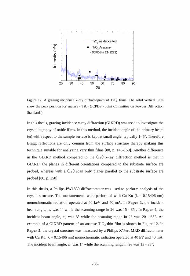
- 38 -
20 30 40 50 60 70 80 90
Inte
nsity
(c/
s)
2θ
TiO2 Anatase
(JCPDS # 21-1272)
TiO2 as deposited
Figure 12. A grazing incidence x-ray diffractogram of TiO2 films. The solid vertical lines
show the peak position for anatase - TiO2 (JCPDS - Joint Committee on Powder Diffraction
Standards).
In this thesis, grazing incidence x-ray diffraction (GIXRD) was used to investigate the
crystallography of oxide films. In this method, the incident angle of the primary beam
(ω) with respect to the sample surface is kept at small angle, typically 1- 5o. Therefore,
Bragg reflections are only coming from the surface structure thereby making this
technique suitable for analyzing very thin films [88, p. 143-159]. Another difference
in the GIXRD method compared to the θ/2θ x-ray diffraction method is that in
GIXRD, the planes in different orientations compared to the substrate surface are
probed, whereas with a θ/2θ scan only planes parallel to the substrate surface are
probed [88, p. 150].
In this thesis, a Philips PW1830 diffractometer was used to perform analysis of the
crystal structure. The measurements were performed with Cu Kα (λ = 0.15406 nm)
monochromatic radiation operated at 40 keV and 40 mA. In Paper 1, the incident
beam angle, ω, was 1° while the scanning range in 2θ was 15 - 85°. In Paper 4, the
incident beam angle, ω, was 3° while the scanning range in 2θ was 20 - 65°. An
example of a GIXRD pattern of an anatase TiO2 thin film is shown in Figure 12. In
Paper 5, the crystal structure was measured by a Philips X’Pert MRD diffractometer
with Cu Kα (λ = 0.15406 nm) monochromatic radiation operated at 40 kV and 40 mA.
The incident beam angle, ω, was 1° while the scanning range in 2θ was 15 - 85°.
-38-
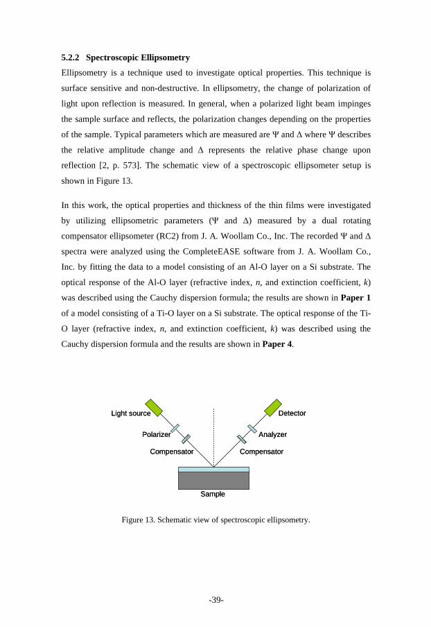
- 39 -
5.2.2 Spectroscopic Ellipsometry
Ellipsometry is a technique used to investigate optical properties. This technique is
surface sensitive and non-destructive. In ellipsometry, the change of polarization of
light upon reflection is measured. In general, when a polarized light beam impinges
the sample surface and reflects, the polarization changes depending on the properties
of the sample. Typical parameters which are measured are Ψ and ∆ where Ψ describes
the relative amplitude change and ∆ represents the relative phase change upon
reflection [2, p. 573]. The schematic view of a spectroscopic ellipsometer setup is
shown in Figure 13.
In this work, the optical properties and thickness of the thin films were investigated
by utilizing ellipsometric parameters (Ψ and ∆) measured by a dual rotating
compensator ellipsometer (RC2) from J. A. Woollam Co., Inc. The recorded Ψ and ∆
spectra were analyzed using the CompleteEASE software from J. A. Woollam Co.,
Inc. by fitting the data to a model consisting of an Al-O layer on a Si substrate. The
optical response of the Al-O layer (refractive index, n, and extinction coefficient, k)
was described using the Cauchy dispersion formula; the results are shown in Paper 1
of a model consisting of a Ti-O layer on a Si substrate. The optical response of the Ti-
O layer (refractive index, n, and extinction coefficient, k) was described using the
Cauchy dispersion formula and the results are shown in Paper 4.
Figure 13. Schematic view of spectroscopic ellipsometry.
Sample
CompensatorCompensator
Polarizer Analyzer
DetectorLight source
Sample
CompensatorCompensator
Polarizer Analyzer
DetectorLight source
-39-
- 40 -
5.2.3 Scanning Electron Microscopy
In scanning electron microscopy (SEM) an electron beam is employed to illuminate
the sample and the backscattered and secondary electrons ejected from the sample are
collected to form an image. The electron beam is produced by heating a metallic
filament (a type of electron source). The electron beam is focused by electromagnetic
lenses which direct the beam down to the sample surface. The electron beam can be
accelerated to energies ranging from 0.5 - 50 keV [2, p. 585]. When the electron beam
hits the sample surface, electrons in the beam can penetrate and lose energy due to
scattering and absorption within a pear-shaped volume inside the sample. The size of
the pear-shaped volume is dependent on the electron energy, atomic number of the
sample element and the sample density. The interaction between the electron beam
and the sample leads to an energy exchange between; this results in the reflection of
high energy electrons (backscattered electron), emission of secondary electrons and
emission of electromagnetic radiation [2, p. 586-589]. In general, the sample should
be electrically conductive to prevent the accumulation of electrostatic charge at the
surface. However, a non-conductive sample can be analyzed via SEM using special
preparation routine. The special preparation usually involves coating the sample with
an ultrathin electrically-conducting material, commonly gold. This coating can
prevent the accumulation of static electrical charge on the sample during electron
irradiation. In this work, SEM was used to look at a sample cross section to measure
the film thickness. The samples in this work such as Al2O3 and TiO2 are non-
conductive. In this thesis we used low energy (3 keV) electron beam instead of
coating the samples with ultrathin gold in order to lower the risks of build-up of static
electric charge.
5.2.4 Elastic Recoil Detector Analysis
In order to investigate the chemical composition and element depth profiles in the
near surface layer of thin films, ion beam analysis can be employed. Elastic recoil
detection analysis (ERDA) is an ion beam based analysis technique which is used for
quantitative analysis of light to medium elements [89]. ERDA uses a heavy ion beam
with energy in the order of several MeV. The incoming beam knocks out atoms in the
sample and the recoiled atoms are picked up by the detector. Typical scattering
geometry is shown in Figure 14. When a projectile of mass M1, atomic number Z1,
and energy E1 collides with an atom of mass M2 and atomic number Z2 in the sample,
-40-
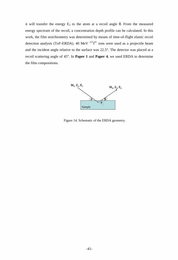
- 41 -
it will transfer the energy E2 to the atom at a recoil angle θ. From the measured
energy spectrum of the recoil, a concentration depth profile can be calculated. In this
work, the film stoichiometry was determined by means of time-of-flight elastic recoil
detection analysis (ToF-ERDA). 40 MeV 127I9+ ions were used as a projectile beam
and the incident angle relative to the surface was 22.5°. The detector was placed at a
recoil scattering angle of 45°. In Paper 1 and Paper 4, we used ERDA to determine
the film compositions.
Figure 14. Schematic of the ERDA geometry.
θα β
M1, Z1, E1 M2, Z2, E2
Sample
θα β
M1, Z1, E1 M2, Z2, E2
Sample
-41-

- 42 -
-42-
- 43 -
Chapter 6
Summary of Results
In this chapter I will summarize the main results of the five included papers and share
my opinion on how this thesis may have contributed to the field of reactive sputtering.
I have conducted research on metal oxides deposited by reactive high power impulse
magnetron sputtering (HiPIMS). Understanding process behavior of reactive HiPIMS
is one of the major ways for improving the deposition process, deposition rate,
process stability and film properties. Direct current magnetron sputtering (DCMS)
was also studied as a comparison to reactive HiPIMS under the similar conditions.
6.1 Fundamentals of Reactive High Power Impulse Magnetron
Sputtering
Paper 1 - Hysteresis and process stability in reactive high power impulse magnetron
sputtering of metal oxides
Al-O and Ce-O systems were used to study the hysteresis effect by reactive HiPIMS
and DCMS. It was found that for the same sputtering conditions, reactive HiPIMS can
eliminate/reduce the hysteresis effect in comparison to DCMS. The stabilization of
the transition zone is observed in the range of frequency (2 and 4 kHz) for Al-O while
for Ce-O, reactive HiPIMS can reduce the hysteresis effect. The main mechanism
proposed to explain this phenomenon is the effect of gas rarefaction and refill time of
-43-
- 44 -
the gas dynamic between the pulses. Moreover, it was found that the stabilization of
the transition zone in HiPIMS is not dependent on the pumping speed of the system.
In order to unravel the effect of the process stability on the film properties, Al2O3
films were grown on Si substrates by reactive HiPIMS and DCMS. A series of films
with thicknesses of about 200 nm was grown varying the oxygen gas flows. Again,
HiPIMS showed a wide stable range to grow the stoichiometric films and the
deposition rate of the films were higher than DCMS. Furthermore, the properties of
films deposited by reactive HiPIMS showed a higher refractive index indicating
higher film density as compared to films deposited by reactive DCMS.
Paper 2 - Studies of hysteresis effect in reactive HiPIMS deposition of oxides
The effect of target area on the hysteresis effect in reactive HiPIMS was investigated
in this work. A Ti-O system was used and the diameter of the Ti target was 100 mm.
The geometry of the system is also different from the system in Paper 1 in order to
compare the characteristic hysteresis curve as related to pulse frequency for different
geometry systems. The results show that although the geometry of the system is
different, reactive HiPIMS can reduce the hysteresis width; also, there is an optimum
frequency to minimize the hysteresis width. The effect of gas rarefaction and gas refill
times are also investigated. The gas rarefaction in front of the target starts to dominate
when the off-time is short enough to prevent the gas refill in front of the target.
Furthermore, gas rarefaction is more pronounced with increasing peak current. In
summary, this paper indicates that the reduction of the hysteresis effect may be very
system dependent.
Paper 3 - Understanding the discharge current behavior in reactive high power
impulse magnetron sputtering of oxides
In this paper, differences in the discharge current behavior in non-reactive and
reactive high power impulse magnetron sputtering of metal oxides, i.e. different
shapes and peak current density, are studied. This work contributes towards
understanding the physics of reactive high power impulse magnetron sputtering
(HiPIMS) processes by studying the discharge current behavior of Ti-O and Al-O.
The understanding was developed by investigating the ionic contributions as well as
the time evolution of the sputtering and reactive gas ions (Ar1+ and O1+ respectively)
and sputtered metal ions (Ti1+ and Al1+) to the discharge current. The effect of
-44-
- 45 -
secondary electron emission yield of metal and oxide target surfaces along with the
influence of the partial sputtering yields for Ar1+, Ti1+, Al1+ and O1+ on the discharge
current were also investigated. It was found that in a reactive HiPIMS process, the
discharge was dominated by ionized oxygen and the energy distribution functions of
the O1+ ions resemble to that of the sputtered metal. It was established that the oxygen
is preferentially sputtered from the target surface which means that the source of O1+
ions was the sputtering target rather than the gas phase. The ionized oxygen
determines the discharge behavior in reactive HiPIMS, and its contribution to the
observed increased discharge currents in oxide mode is vital. Another important
finding of this paper is the observation that a strong gas depletion regime is never
reached when operating in the oxide mode. The experimental observations of this
research were also supported by TRIDYN simulations.
6.2 Growth Using Reactive High Power Impulse Magnetron
Sputtering
Paper 4 - Effect of peak power in reactive high power impulse magnetron
sputtering of titanium dioxide
In this paper, the effect of peak power on the properties of TiO2 films grown by
reactive HiPIMS and DCMS was investigated. For constant average power and pulse
on-time, the change in pulse frequency led to a change in the peak power. That is, the
peak power increased with decreased pulse frequency. It was found that it was
possible to control the phase composition via the HiPIMS peak power, and films
containing pure anatase, pure rutile and a mixture between anatase and rutile phases
were grown. Furthermore, the ion composition and their energy distributions were
analyzed using energy resolved mass spectrometry. The ion energy distributions
showed that O ions in the plasma were more energetic than the Ti ions. The
crystallinity and variation in the phase composition of TiO2 films depended on the
energy of the arriving particles (mainly ionized species). TiO2 films deposited by
reactive HiPIMS showed superior properties to the films deposited by DCMS, i.e., a
higher refractive index and a higher film density. The deposition rate is a small lost in
HiPIMS as compared to DCMS.
-45-
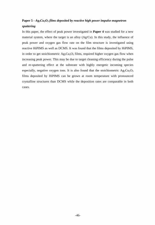
- 46 -
Paper 5 - Ag2Cu2O3 films deposited by reactive high power impulse magnetron
sputtering
In this paper, the effect of peak power investigated in Paper 4 was studied for a new
material system, where the target is an alloy (Ag/Cu). In this study, the influence of
peak power and oxygen gas flow rate on the film structure is investigated using
reactive HiPIMS as well as DCMS. It was found that the films deposited by HiPIMS,
in order to get stoichiometric Ag2Cu2O3 films, required higher oxygen gas flow when
increasing peak power. This may be due to target cleaning efficiency during the pulse
and re-sputtering effect at the substrate with highly energetic incoming species
especially, negative oxygen ions. It is also found that the stoichiometric Ag2Cu2O3
films deposited by HiPIMS can be grown at room temperature with pronounced
crystalline structures than DCMS while the deposition rates are comparable in both
cases.
-46-
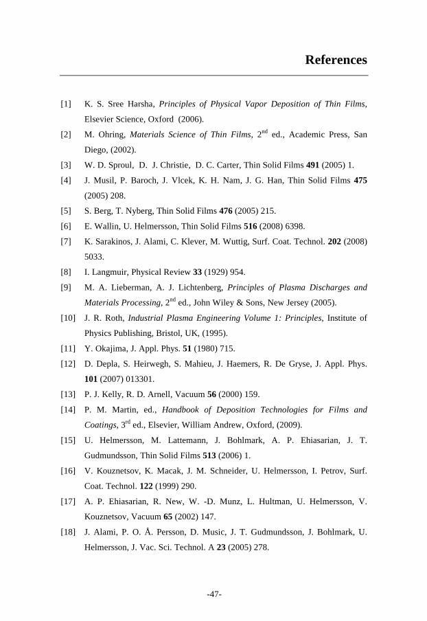
- 47 -
References
[1] K. S. Sree Harsha, Principles of Physical Vapor Deposition of Thin Films,
Elsevier Science, Oxford (2006).
[2] M. Ohring, Materials Science of Thin Films, 2nd ed., Academic Press, San
Diego, (2002).
[3] W. D. Sproul, D. J. Christie, D. C. Carter, Thin Solid Films 491 (2005) 1.
[4] J. Musil, P. Baroch, J. Vlcek, K. H. Nam, J. G. Han, Thin Solid Films 475
(2005) 208.
[5] S. Berg, T. Nyberg, Thin Solid Films 476 (2005) 215.
[6] E. Wallin, U. Helmersson, Thin Solid Films 516 (2008) 6398.
[7] K. Sarakinos, J. Alami, C. Klever, M. Wuttig, Surf. Coat. Technol. 202 (2008)
5033.
[8] I. Langmuir, Physical Review 33 (1929) 954.
[9] M. A. Lieberman, A. J. Lichtenberg, Principles of Plasma Discharges and
Materials Processing, 2nd ed., John Wiley & Sons, New Jersey (2005).
[10] J. R. Roth, Industrial Plasma Engineering Volume 1: Principles, Institute of
Physics Publishing, Bristol, UK, (1995).
[11] Y. Okajima, J. Appl. Phys. 51 (1980) 715.
[12] D. Depla, S. Heirwegh, S. Mahieu, J. Haemers, R. De Gryse, J. Appl. Phys.
101 (2007) 013301.
[13] P. J. Kelly, R. D. Arnell, Vacuum 56 (2000) 159.
[14] P. M. Martin, ed., Handbook of Deposition Technologies for Films and
Coatings, 3rd ed., Elsevier, William Andrew, Oxford, (2009).
[15] U. Helmersson, M. Lattemann, J. Bohlmark, A. P. Ehiasarian, J. T.
Gudmundsson, Thin Solid Films 513 (2006) 1.
[16] V. Kouznetsov, K. Macak, J. M. Schneider, U. Helmersson, I. Petrov, Surf.
Coat. Technol. 122 (1999) 290.
[17] A. P. Ehiasarian, R. New, W. -D. Munz, L. Hultman, U. Helmersson, V.
Kouznetsov, Vacuum 65 (2002) 147.
[18] J. Alami, P. O. Å. Persson, D. Music, J. T. Gudmundsson, J. Bohlmark, U.
Helmersson, J. Vac. Sci. Technol. A 23 (2005) 278.
-47-
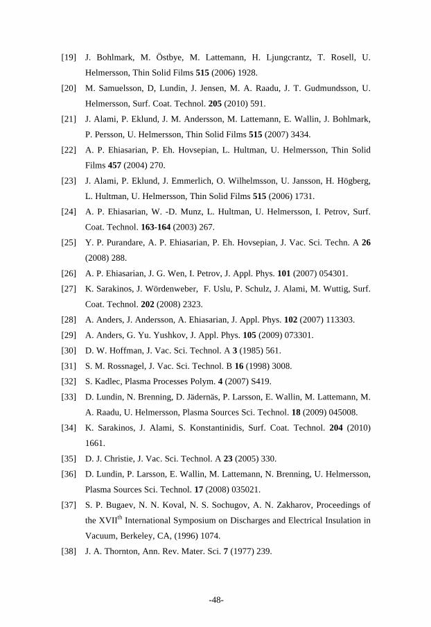
- 48 -
[19] J. Bohlmark, M. Östbye, M. Lattemann, H. Ljungcrantz, T. Rosell, U.
Helmersson, Thin Solid Films 515 (2006) 1928.
[20] M. Samuelsson, D, Lundin, J. Jensen, M. A. Raadu, J. T. Gudmundsson, U.
Helmersson, Surf. Coat. Technol. 205 (2010) 591.
[21] J. Alami, P. Eklund, J. M. Andersson, M. Lattemann, E. Wallin, J. Bohlmark,
P. Persson, U. Helmersson, Thin Solid Films 515 (2007) 3434.
[22] A. P. Ehiasarian, P. Eh. Hovsepian, L. Hultman, U. Helmersson, Thin Solid
Films 457 (2004) 270.
[23] J. Alami, P. Eklund, J. Emmerlich, O. Wilhelmsson, U. Jansson, H. Högberg,
L. Hultman, U. Helmersson, Thin Solid Films 515 (2006) 1731.
[24] A. P. Ehiasarian, W. -D. Munz, L. Hultman, U. Helmersson, I. Petrov, Surf.
Coat. Technol. 163-164 (2003) 267.
[25] Y. P. Purandare, A. P. Ehiasarian, P. Eh. Hovsepian, J. Vac. Sci. Techn. A 26
(2008) 288.
[26] A. P. Ehiasarian, J. G. Wen, I. Petrov, J. Appl. Phys. 101 (2007) 054301.
[27] K. Sarakinos, J. Wördenweber, F. Uslu, P. Schulz, J. Alami, M. Wuttig, Surf.
Coat. Technol. 202 (2008) 2323.
[28] A. Anders, J. Andersson, A. Ehiasarian, J. Appl. Phys. 102 (2007) 113303.
[29] A. Anders, G. Yu. Yushkov, J. Appl. Phys. 105 (2009) 073301.
[30] D. W. Hoffman, J. Vac. Sci. Technol. A 3 (1985) 561.
[31] S. M. Rossnagel, J. Vac. Sci. Technol. B 16 (1998) 3008.
[32] S. Kadlec, Plasma Processes Polym. 4 (2007) S419.
[33] D. Lundin, N. Brenning, D. Jädernäs, P. Larsson, E. Wallin, M. Lattemann, M.
A. Raadu, U. Helmersson, Plasma Sources Sci. Technol. 18 (2009) 045008.
[34] K. Sarakinos, J. Alami, S. Konstantinidis, Surf. Coat. Technol. 204 (2010)
1661.
[35] D. J. Christie, J. Vac. Sci. Technol. A 23 (2005) 330.
[36] D. Lundin, P. Larsson, E. Wallin, M. Lattemann, N. Brenning, U. Helmersson,
Plasma Sources Sci. Technol. 17 (2008) 035021.
[37] S. P. Bugaev, N. N. Koval, N. S. Sochugov, A. N. Zakharov, Proceedings of
the XVIIth International Symposium on Discharges and Electrical Insulation in
Vacuum, Berkeley, CA, (1996) 1074.
[38] J. A. Thornton, Ann. Rev. Mater. Sci. 7 (1977) 239.
-48-
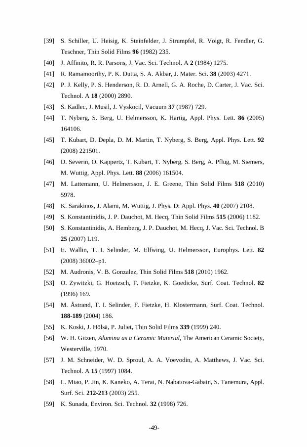
- 49 -
[39] S. Schiller, U. Heisig, K. Steinfelder, J. Strumpfel, R. Voigt, R. Fendler, G.
Teschner, Thin Solid Films 96 (1982) 235.
[40] J. Affinito, R. R. Parsons, J. Vac. Sci. Technol. A 2 (1984) 1275.
[41] R. Ramamoorthy, P. K. Dutta, S. A. Akbar, J. Mater. Sci. 38 (2003) 4271.
[42] P. J. Kelly, P. S. Henderson, R. D. Arnell, G. A. Roche, D. Carter, J. Vac. Sci.
Technol. A 18 (2000) 2890.
[43] S. Kadlec, J. Musil, J. Vyskocil, Vacuum 37 (1987) 729.
[44] T. Nyberg, S. Berg, U. Helmersson, K. Hartig, Appl. Phys. Lett. 86 (2005)
164106.
[45] T. Kubart, D. Depla, D. M. Martin, T. Nyberg, S. Berg, Appl. Phys. Lett. 92
(2008) 221501.
[46] D. Severin, O. Kappertz, T. Kubart, T. Nyberg, S. Berg, A. Pflug, M. Siemers,
M. Wuttig, Appl. Phys. Lett. 88 (2006) 161504.
[47] M. Lattemann, U. Helmersson, J. E. Greene, Thin Solid Films 518 (2010)
5978.
[48] K. Sarakinos, J. Alami, M. Wuttig, J. Phys. D: Appl. Phys. 40 (2007) 2108.
[49] S. Konstantinidis, J. P. Dauchot, M. Hecq, Thin Solid Films 515 (2006) 1182.
[50] S. Konstantinidis, A. Hemberg, J. P. Dauchot, M. Hecq, J. Vac. Sci. Technol. B
25 (2007) L19.
[51] E. Wallin, T. I. Selinder, M. Elfwing, U. Helmersson, Europhys. Lett. 82
(2008) 36002–p1.
[52] M. Audronis, V. B. Gonzalez, Thin Solid Films 518 (2010) 1962.
[53] O. Zywitzki, G. Hoetzsch, F. Fietzke, K. Goedicke, Surf. Coat. Technol. 82
(1996) 169.
[54] M. Åstrand, T. I. Selinder, F. Fietzke, H. Klostermann, Surf. Coat. Technol.
188-189 (2004) 186.
[55] K. Koski, J. Hölsä, P. Juliet, Thin Solid Films 339 (1999) 240.
[56] W. H. Gitzen, Alumina as a Ceramic Material, The American Ceramic Society,
Westerville, 1970.
[57] J. M. Schneider, W. D. Sproul, A. A. Voevodin, A. Matthews, J. Vac. Sci.
Technol. A 15 (1997) 1084.
[58] L. Miao, P. Jin, K. Kaneko, A. Terai, N. Nabatova-Gabain, S. Tanemura, Appl.
Surf. Sci. 212-213 (2003) 255.
[59] K. Sunada, Environ. Sci. Technol. 32 (1998) 726.
-49-
- 50 -
[60] A. Fujishima, T. N. Rao, D. A. Tryk, J. Photochem. Photobiol. C 1 (2000) 1.
[61] T. Lindgren, J. M. Mwabora, E. Avendano, J. Jonsson, A. Hoel, C. G.
Granqvist, S. E. Lindquist, J. Phys. Chem. B 107 (2003) 5709.
[62] M. D. Wiggins, M. C. Nelson, C. R. Aita, J. Vac. Sci. Technol. A 14 (1996)
772.
[63] D. Wicaksana, A. Kobayashi, A. Kinbara, J. Vac. Sci. Technol. A 10 (1992)
1479.
[64] V. Straňák, M. Quaas, H. Wulff, Z. Hubička, S. Wrehde, M. Tichý, R. Hippler,
J. Phys. D: Appl. Phys. 41 (2008) 055202.
[65] M. Mogensen, N. M. Sammes, G. A. Tompsett, 129 (2000) 63.
[66] L. Tye, N. A. El-Masry, T. Chikyow, P. Mclarty, S. M. Bedair, Appl. Phys.
Lett. 65 (1994) 3081.
[67] F. C. Fonseca, S. Uhlenbruck, R. Nédélec, D. Sebold, H. P. Buchkremer, J.
Electrochem. Soc. 157 (2010) B1515.
[68] S. Kanakaraju, S. Mohan, A. K. Sood, Thin Solid Films 305 (1997) 191.
[69] P. Jasinski, T. Suzuki, H. U. Anderson, Sens. Actuators, B 95 (2003) 73.
[70] Y.-L. Kuo, C. Lee, Y.-S. Chen, H. Liang, Solid State Ionics 180 (2009) 1421.
[71] V. Matolín, J. Libra, I. Matolínová, V. Nehasil, L. Sedláček, F. Šutara, Appl.
Surf. Sci. 254 (2007) 153.
[72] T. Inoue, Y. Yamamotob, M. Satoh, Thin Solid Films 343-344 (1999) 594.
[73] V. Trtik, R. Aguiar, F. Sanchez, C. Ferrater, M. Varela, 192 (1998).
[74] N. Özer, Sol. Energy Mater. Sol. Cells 68 (2001) 391.
[75] L. Kim, J. Kim, D. Jung, C. Y. Park, C. W. Yang, Y. Roh, Thin Solid Films
360 (2000) 154.
[76] O. Nakagawara, M. Kobayashi, Y. Yoshino, Y. Katayama, H. Tabata, T.
Kawai, J. Appl. Phys. 78 (1995) 7226.
[77] P. Gomez-Romero, E. M. Tejada-Rosales, M. Rosa Palacin, Angew. Chem. Int.
Ed. 38 (1999) 524.
[78] J. F. Pierson, D. Wiederkehr, J.-M. Chappé, N. Martin, Appl. Surf. Sci. 253
(2006) 1484.
[79] J. Feng, B. Xiao, J. C. Chen, C. T. Zhou, Y. P. Du, R. Zhou, Solid State
Commun. 149 (2009) 1569.
[80] J. F. Pierson, D. Horwat, Appl. Surf. Sci. 253 (2007) 7522.
-50-
- 51 -
[81] S. Uthanna, M. H. P. Reddy, P. Boulet, C. Petitjean, J. F. Pierson, Phys. Status
Solidi A 207 (2010) 1655.
[82] J. F. Pierson, E. Rolin, C. Clément-Gendarme, C. Petitjean, D. Horwat, Appl.
Surf. Sci. 254 (2008) 6590.
[83] E. Lund, A. Galeckas, E. V. Monakhov, B. G. Svensson, Thin Solid Films 520
(2011) 230.
[84] C. Petitjean, D. Horwat, J. F. Pierson, Appl. Surf. Sci. 255 (2009) 7700.
[85] M. Hari Prasad Reddy, J. F. Pierson, S. Uthanna, Cryst. Res. Technol. 46
(2011) 1329.
[86] K. Ellmer, R. Wendt, K. Wiesemann, Int. J. Mass Spectrom. 223-224 (2003)
679.
[87] S. Seeger, K. Harbauer, K. Ellmer, J. Appl. Phys. 105 (2009) 053305.
[88] M. Birkholz, Thin Film Analysis by X-Ray Scattering, Wiley-VCH, Weinheim,
(2006).
[89] D. D. Cohen, R. Bird, N. Dytlewski, R. Siegele, Encycl. Phys. Sci. &
Technol., Academic Press, (2001).
-51-


![[PPT]Home-Made DC Magnetron Sputtering System - …faculty.kfupm.edu.sa/.../research_files/magnetron.ppt · Web viewHome-Made DC Magnetron Sputtering System Chamber and Gas supply](https://img.dokumen.tips/doc/110x75/5aa9b1b37f8b9a90188d2f45/ppthome-made-dc-magnetron-sputtering-system-viewhome-made-dc-magnetron-sputtering.jpg)