Embed Size (px)
Citation preview

Rapid Prototyping System for Control of Inverters
and Electrical Drives
Vom FachbereichElektrotechnik, Informationstechnik und Medientechnik
der Bergischen Universität Wuppertalzur Erlangung des akademischen Grades eines
Doktor-Ingenieursgenehmigte Dissertation
vorgelegt vonmgr inż. Paweł Szczupak
aus Warschau, Polen
Wuppertal, 2008

Diese Dissertation kann wie folgt zitiert werden: urn:nbn:de:hbz:468-20080686 [http://nbn-resolving.de/urn/resolver.pl?urn=urn%3Anbn%3Ade%3Ahbz%3A468-20080686]

Acknowledgments
The work presented in this thesis was carried out during my Ph.D.
studies at the Institute for Electrical Machines and Drives at the Wup-
pertal University.
First of all I would like to thank my whole family, particularly my wife
Agnieszka for her love, patience and support.
I would like to thank Prof. Ralph Kennel for having accepted me in
his Institute and for undertaking the direction of this thesis. Next, I
thank sincerely Prof. Mario Pacas, from the University of Siegen, who
took in charge the coexamination.
I am also grateful to my colleagues at the EMAD Laboratory who
helped me during my stay at the Wuppertal University.

Contents
1 Introduction 1
2 Control systems 3
2.1 Digital Signal Processor or microcontroller . . . . . . . . . 3
2.2 Commercially available solution . . . . . . . . . . . . . . . 7
2.3 Embedded computers . . . . . . . . . . . . . . . . . . . . 8
3 Hardware description 17
3.1 19inch Rack and power supply . . . . . . . . . . . . . . . 17
3.2 PC/104 CPU module . . . . . . . . . . . . . . . . . . . . . 19
3.3 Interface card . . . . . . . . . . . . . . . . . . . . . . . . . 21
3.4 Bus Board . . . . . . . . . . . . . . . . . . . . . . . . . . . 25
3.5 PWM Card . . . . . . . . . . . . . . . . . . . . . . . . . . 26
3.5.1 Master - Slave operation of the PWM cards . . . . 34
3.5.2 Interrupt latency . . . . . . . . . . . . . . . . . . . 37
3.6 A/D and D/A cards . . . . . . . . . . . . . . . . . . . . . 39
3.7 HEX card . . . . . . . . . . . . . . . . . . . . . . . . . . . 41
4 Software description 43
4.1 Operating system . . . . . . . . . . . . . . . . . . . . . . . 43
4.2 Kernel space and user space . . . . . . . . . . . . . . . . . 46
4.3 Real-time operation . . . . . . . . . . . . . . . . . . . . . 47
4.4 RTAI installation . . . . . . . . . . . . . . . . . . . . . . . 48
4.5 PC/104 control program . . . . . . . . . . . . . . . . . . . 51
I

Contents
5 Sensorless control of active rectifiers 55
5.1 Introduction . . . . . . . . . . . . . . . . . . . . . . . . . . 55
5.2 Voltage Oriented Control . . . . . . . . . . . . . . . . . . 57
5.3 Grid Voltage Estimation by Phase Tracking . . . . . . . . 60
5.4 Experimental results . . . . . . . . . . . . . . . . . . . . . 62
5.4.1 Grid inductance value mismatch . . . . . . . . . . 63
5.4.2 Supply voltage distortions . . . . . . . . . . . . . . 64
5.5 Phase disconnection problem . . . . . . . . . . . . . . . . 71
5.6 PC/104 system . . . . . . . . . . . . . . . . . . . . . . . . 76
6 Sensorless Speed / Position Control of Servo Motors 77
6.1 Introduction . . . . . . . . . . . . . . . . . . . . . . . . . . 77
6.2 Alternating carrier injection principle . . . . . . . . . . . . 78
6.3 Estimation of the anisotropy . . . . . . . . . . . . . . . . 79
6.4 Sensorless control approach . . . . . . . . . . . . . . . . . 81
6.4.1 Demodulation of the carrier current . . . . . . . . 81
6.4.2 Sensorless position control of SMPMSM . . . . . . 82
6.4.3 Experimental results . . . . . . . . . . . . . . . . . 83
6.5 PC/104 system . . . . . . . . . . . . . . . . . . . . . . . . 84
7 Model-based predictive control for electrical drives 85
7.1 Introduction . . . . . . . . . . . . . . . . . . . . . . . . . . 85
7.2 Cascaded Control of Induction Motor with PI Controllers 87
7.3 Predictive control . . . . . . . . . . . . . . . . . . . . . . . 88
7.4 Experimental results . . . . . . . . . . . . . . . . . . . . . 91
7.5 PC/104 system . . . . . . . . . . . . . . . . . . . . . . . . 95
8 Conclusions 97
Bibliography 99
II

Contents
A PC/104 control program example 103
B Interface card GAL program 111
C VHDL program for FPGA on the PWM card 115
III

IV

List of Figures
3.1 Schematic of a typical switching-mode power supply unit 18
3.2 Slots of the Bus Board: a) PC/104 module slot, b) expan-
sion card slot . . . . . . . . . . . . . . . . . . . . . . . . . 26
3.3 Scheme of a 2-level inverter . . . . . . . . . . . . . . . . . 27
3.4 Scheme of the operation of the PWM card . . . . . . . . . 29
3.5 Generation of the PWM signals . . . . . . . . . . . . . . . 29
3.6 Sinusoidal PWM generation . . . . . . . . . . . . . . . . . 30
3.7 Space vectors in a complex plane . . . . . . . . . . . . . . 31
3.8 Dead-time . . . . . . . . . . . . . . . . . . . . . . . . . . . 33
3.9 Necessary connection of PWM cards for Master-Slave op-
eration . . . . . . . . . . . . . . . . . . . . . . . . . . . . . 35
3.10 Output pulses of one phase of Master and Slave PWM cards 36
3.11 Time shift between Master and Slave PWM signals . . . . 37
3.12 Interrupt latency of PC/104 system . . . . . . . . . . . . 38
3.13 Analog to digital converter card . . . . . . . . . . . . . . . 39
3.14 Digital to analog converter card . . . . . . . . . . . . . . . 40
4.1 Typical structure of a kernel module for PC/104 system . 52
5.1 3-phase sensorless PWM input rectifier . . . . . . . . . . . 56
5.2 Model of the PWM rectifier system . . . . . . . . . . . . . 57
5.3 Sensorless Voltage Oriented Control . . . . . . . . . . . . 58
5.4 Coordinate transformation from fixed αβ to rotating dq
reference frame . . . . . . . . . . . . . . . . . . . . . . . . 59
V

List of Figures
5.5 Grid voltage estimation through phase tracking . . . . . . 60
5.6 Measured δ and estimated δ angle, and error between them 63
5.7 Influence of the grid inductance on the sensorless control
system . . . . . . . . . . . . . . . . . . . . . . . . . . . . . 64
5.8 Line currents (αβ) and supply voltage vector angle by 2%
unbalanced grid voltage . . . . . . . . . . . . . . . . . . . 66
5.9 Line currents (αβ) and supply voltage vector angle by 6%
unbalanced grid voltage . . . . . . . . . . . . . . . . . . . 67
5.10 Line currents (αβ) and supply voltage vector angle by
10% over-voltage . . . . . . . . . . . . . . . . . . . . . . . 69
5.11 Line currents (αβ) and supply voltage vector angle by
65% under-voltage . . . . . . . . . . . . . . . . . . . . . . 71
5.12 Single grid phase (L3) disconnection . . . . . . . . . . . . 72
5.13 Control of the PWM rectifier in case of phase disconnection 73
5.14 Voltage angle δ . . . . . . . . . . . . . . . . . . . . . . . . 74
5.15 Reaction of the system on the L3 phase disconnection . . 75
6.1 Resulting current signal ic as a modulated space vector
in rotor coordinates . . . . . . . . . . . . . . . . . . . . . 78
6.2 Signal flow graph of the field angle estimation scheme
based on the proposed method . . . . . . . . . . . . . . . 82
6.3 Experimental results: rotor position δ and corresponding
estimated variables δ, ∆δ . . . . . . . . . . . . . . . . . . 83
7.1 Structure of a typical cascaded controller . . . . . . . . . 86
7.2 Field-oriented drive control with PI controllers . . . . . . 88
7.3 Typical structure of a predictive controller . . . . . . . . . 90
7.4 Typical structure of a MPC controller . . . . . . . . . . . 91
7.5 Current control: Large signal response . . . . . . . . . . . 92
7.6 Current control: Small signal response . . . . . . . . . . . 93
VI

List of Figures
7.7 Current control: Large signal response at ω = 0.4 . . . . . 94
VII

VIII

1 Introduction
Nowadays in academic laboratories DSP-based solutions are used for
developing control methods. These systems provide very small latencies
and excellent performance. The main drawback of such a system is its
price. Also there is a software bundle, which has to be bought. The price
of the software is very often much higher than the cost of the hardware.
For an academic laboratory this is a real barrier and only few laboratory
projects can be equipped with such a system. There is also a problem
with respect to the limited possibility to expand standard DSP systems.
The user has limited number of PWM outputs, A/D converters making
these systems less flexible for research. Therefore there is a need to
provide a better solution. The idea is to use a PC/104 based system,
which can work in real-time environment. The PC/104 is very well
known in the industry, so academic projects can be directly implemented
in industrial environment. For the real-time environment the cost-free
Linux based system with a free RTAI (Real-Time Application Interface,
see chapter 4, section 4.3) extension is used. In this work the proposed
system is presented. Some application examples are presented as well.
1

2

2 Control systems
2.1 Digital Signal Processor or microcontroller
Very often academic and industrial laboratories are using specialized Dig-
ital Signal Processors in their control systems. Digital signal processing
is a study of digital signals and their processing. Historically the origins
of signal processing are in electrical engineering, and a signal here means
an electrical signal carried by a wire or telephone line, or perhaps by a
radio wave. More generally, however, a signal is a stream of information
representing anything from stock prices to data from a remote-sensing
satellite. The processing of a digital signal is done by performing nu-
merical calculations. The introduction of the microprocessor in the late
1970’s and early 1980’s made it possible for DSP techniques to be used
in a much wider range of applications. During the 1980’s the increasing
importance of DSP led several major electronics manufacturers
• Texas Instruments with C6000 DSP family
• Reneasys with SuperH DPS family
• Freescale with SuperCore DSP family
to develop Digital Signal Processor chips - specialized microprocessors
with architectures designed specifically for the types of operations re-
quired in digital signal processing. These specialized processors are pro-
cessing data mostly using fixed-point arithmetic, but there are also pro-
cessors where floating-point arithmetic is implemented. Although some
3

2 Control systems
of the mathematical theory underlying DSP techniques, such as Fourier
and Hilbert Transforms, digital filter design and signal compression, can
be fairly complex, the numerical operations required actually to imple-
ment these techniques are very simple. The architecture of a DSP chip
is designed to carry out such operations incredibly fast, processing hun-
dreds of millions of samples every second, to provide real-time perfor-
mance: that is, the ability to process a signal "live" as it is sampled and
then output the processed signal, for example to a loudspeaker or video
display. The DSPs are mostly used in such scientific areas as [3]:
• space (space photograph enhancement)
• medical (diagnostic imaging)
• military (radar, sonar)
• commercial (special video effects)
• telecommunication (voice compression)
and many other. For the control of electric drives and inverters the DSPs
are more and more used. The reasons for their popularity in this field
are:
• very low latencies (the reaction speed of the DSP on a trigger signal
is very high)
• very high calculation power
• programming flexibility
Although price of the processors is constantly falling, there are some
disadvantages of this solution:
4

2.1 Digital Signal Processor or microcontroller
• very high cost of the software used to program the DSPs (important
especially for the universities)
• long learning time (very important point for the academic labora-
tories, where students work in their projects)
• limited expansion possibility
In new projects it is not always known at the beginning how many in-
puts/outputs are needed. DSPs for have limited number of the PWM
outputs, which are necessary for inverter control. Some digital signal
processors have on-chip analog to digital converters, there is no possi-
bility to exchange them or to install additional A/D converters if more
signals have to be measured. Of course external A/D converters can be
used, but this increases cost of the system. Certainly a digital signal
processor alone is not enough to build any control system. Additional
hardware has to be designed or bought in order to set up a control sys-
tem.
Digital signal processors are not capable of multitasking. They are
able to process one program at a time. Therefore another system is
needed if - for example - a Graphical User Interface is used. It is mostly
a PC where necessary software is installed. This PC can also be used to
program the DSP. So for every laboratory project a PC has to be bought
with a license for the DSP software. As written before cost of the DSP
software is sometimes much higher than cost of the DSP itself. Naturally
one PC with one software license would be sufficient to program many
DSPs. But in case there are many students in the laboratory, each of
them has his own project and these projects are not connected together.
So each student has to write a piece of his code, program the DSP, install
the processor in his project and test its functioning. If there are errors,
the user has to remove DSP from project’s hardware and take it back
5

2 Control systems
to the PC to correct there the wrong code, program the DSP again and
again test it in the project. Such a laboratory work cannot be described
as optimal.
Consequently although DSPs have many advantages and can be suc-
cessfully used in many projects, the high cost and low hardware flexi-
bility makes them uninteresting for a research laboratory where many
different projects are performed. An example price of an development
bundle (DSP equipped evaluation board and software for it) from Spec-
trumDigital Inc. range from: 775USD for a simple TMS320F2812 DSP
to 9995USD for TI processor from C6000 family1. These complete bun-
dles need additional hardware if they are used for inverter and drive con-
trol. As mentioned above another PC with licensed software is needed
for software bundle.
Microcontrollers are processors developed especially for control pur-
poses. Unlike DSPs almost every microcontroller is equipped with on-
chip A/D converters and has many other I/O ports. Although their
processing power is not as high as of DSPs it is sufficient for standard
industry projects. The latency times of microcontrollers are also very
short. But the same disadvantages as for the DSP processors exist. Mi-
crocontrollers need additional hardware to work. A PC is needed with
dedicated software to program the devices. Very often it is necessary
to program in assembly language, what makes the microcontroller hard
to learn for students. More time is needed to master it. The microcon-
troller based system cannot be flexibly set up for different projects. The
PWM outputs number is also limited by the chip itself.
1http://www.spectrumdigital.com
6

2.2 Commercially available solution
2.2 Commercially available solution
Among the commercially available solutions one is very often mentioned
in publications. It is a product of a dSPACE company. The most popular
is a DS1103 card. It is an ISA standard card, which has to be installed
into a Personal Computer. The important elements of this card are listed
below:
• Motorola PowerPC 604e / 400 MHz Superscalar microprocessor
• 2 general purpose timers
• 2MB program memory and 128MB data memory
• interrupts by host PC, CAN, slave DSP, serial interface, incremen-
tal encoders and 4 external inputs, PWM synchronous interrupts
• analog inputs: 16 channels 16-bit, 4 to 1 multiplexed, 4 sam-
ple&hold units, 4 ms sampling time; 4 channels 12-bit, sam-
ple&hold, 800 ns sampling time; ±10V input voltage range
• analog outputs: 8 channels 14-bit, 5 ms settling time, ±10 V output
voltage range
• 4 channels 8-bit digital I/O port individually programmable
• 6 channel incremental encoder input
• serial and CAN interfaces
• Texas Instruments DSP TMS320F240, 20 MHz, designed for motor
control
It can be seen from the parameters, that the DS1103 card is a combina-
tion of the very powerful RISC processor and the DSP processor from
7

2 Control systems
Texas Instruments. The DS1103 card should be bought with software
kit for programming the card. There is also special software to program
Graphical User Interface for projects, where DS1103 card is used. It is
possible to create a control desktop, where parameters of the running
control program can be changed or results of the measurements can be
shown. The latencies existing in this system are very low, with respect to
the use of the digital signal processor. Even though there are very many
advantages of this setup, there is one very important disadvantage. The
cost of the special academic license for a kit where DS1103 card with
software reaches about 9240EUR2. For this reason not every laboratory
can allow itself to buy such a system.
As written at the beginning of the chapter, the DS1103 card needs
a PC to work. Software for programming the card has to be installed
on this PC also. This is another cost for a laboratory. And just like in
previous solution one card for a whole laboratory would not be sufficient.
2.3 Embedded computers
Embedded systems are combinations of software and hardware designed
for one or few dedicated tasks. Any kind of processor can be used in
these systems, beginning from simple 8-bit processors and ending with
fast DSPs. Due to the fact, that embedded systems are tailored for
a special task, they can be optimized in their size. Their cost can be
reduced or reliability can be increased. Thus these systems are used in
such products like MP3 players from one side and factory controllers
from the other side.
Many embedded systems are equipped with peripherals to communi-
cate with other devices, for example:
2from: http://www.tobl.krakow.pl/
8

2.3 Embedded computers
• Serial Communication Interfaces (SCI): RS-232, RS-422, RS-485
• Synchronous Serial Communication Interface: I2C, JTAG, SPI,
SSC and ESSI
• Universal Serial Bus (USB)
• Analog to Digital/Digital to Analog (ADC/DAC)
• General Purpose Input/Output (GPIO)
• PLL(s), Capture/Compare and Time Processing Units
• Ethernet, Controller Area Network
Depending on the processor installed in the embedded system it can
work with PC standard operating systems (Microsoft Windows, Linux),
real-time operating systems (MaRTE OS, Helium RTOS, Salvo, DrRtos,
NuttX RTOS and many more) or systems made specially for embedded
computers (DRYOS, FreeDOS, SymbianOS, Windows XP Embedded).
Because embedded systems got very popular, there was a need to
propose a standard for connectors and dimensions. One of the accepted
standards suggested by PC/104 Consortium is called PC/104. It defines
form factor of the system as well as computer bus. Modules in PC/104
standard can be of two bus types: 8-, and 16-bit. There is no backplane
in the PC/104 system, all components are stacked together using the
bus connectors. Signals of the bus connectors are compatible with PC
ISA signals3:
3from ISA and EISA Theory and Operation by Edward Solari
9

2 Control systems
Signal name Signal description
BALE
Bus Address Latch Enable line is driven
by the platform CPU to indicate when
SA<19:0>, LA<23:17>, AENx, and
SBHE# are valid. It is also driven to a
logical one when an ISA add-on card or
DMA controller owns the bus.
SA<19:0>
Address lines are driven by the ISA bus
master to define the lower 20 address sig-
nal lines needed for the lower 1 MB of the
memory address space.
LA<23:17>
Latched Address lines are driven by the
ISA bus master or DMA controller to pro-
vide the additional address lines required
for the 16 MB memory address space.
SBHE#
System Byte High Enable line is driven by
the ISA bus master to indicate that valid
data resides on the SD<15:8> lines.
10

2.3 Embedded computers
AENx
Address Enable line is driven by the plat-
form circuitry as an indication to ISA re-
sources not to respond to the ADDRESS
and I/O COMMAND lines. This line is
the method by which I/O resources are
informed that a DMA transfer cycle is oc-
curring and that only the I/O resource
with an active DACKx# signal line can
respond to the I/O signal lines.
SD<15:0>
Data lines 0 - 7 or 8 - 15 are driven for an
8 data bit cycle, and 0 - 15 are driven for
a 16 data bit cycle.
MEMR#
Memory Read line is driven by the ISA
bus master or DMA controller to request
a memory resource to drive data onto the
bus during the cycle.
SMEMR#
System Memory Read line is to request
a memory resource to drive data onto
the bus during the cycle. This line is
active when MEMR# is active and the
LA<23:20> signal lines indicate the first
1 MB of address space.
MEMW#
Memory Write line is to request a me-
mory resource to accept data from the
data lines.
11

2 Control systems
SMEMW#
System Memory Write line is to request
a memory resource to drive data onto
the bus during the cycle. This line is
active when MEMW# is active and the
LA<23:20> signal lines indicate the first
1 MB of address space.
IOR#
I/O Read line is driven by the ISA bus
master or DMA controller to request an
I/O resource to drive data onto the data
bus during the cycle.
IOW#I/O Write requests an I/O resource to ac-
cept data from the data bus.
MEMCS16#
Memory Chip Select 16 line is driven by
the memory resource to indicate that it is
an ISA resource that supports a 16 data
bit access cycle. It also allows the ISA bus
master to execute shorter cycles.
IOCS16#
I/O Chip Select 16 line is driven by an
I/O resource to indicate that it is an ISA
resource that supports a 16 data bit access
cycle. It also allows the ISA bus master
to execute shorter default cycles.
IOCHRDY
I/O Channel Ready line allows resources
to indicate to the ISA bus master that
additional cycle time is required.
12

2.3 Embedded computers
SRDY#
Synchronous Ready (or NOWS#) line is
driven active by the accessed resource to
indicate that an access cycle shorter than
the standard access cycle can be executed.
REFRESH#Memory Refresh is driven by the refresh
controller to indicate a refresh cycle.
MASTER16#
MASTER16# line is only driven active by
an ISA add-on bus owner card that has
been granted bus ownership by the DMA
controller.
IOCHK#
I/O Channel Check line is driven by any
resource. It is active for a general error
condition that has no specific interpreta-
tion.
RESET
Reset line is driven active by the platform
circuitry. Any bus resource that senses
an active RESET signal line must imme-
diately tri-state all output drivers and en-
ter the appropriate reset condition.
BCLK
System Bus Clock line is a clock driven
by the platform circuitry. It has a 50% ±approximately 5% (57 to 69 nanoseconds
for 8 MHz) duty cycle, at a frequency of
6 to 8 MHz (± 500 ppm).
13

2 Control systems
OSC
Oscillator line is a clock driven by the
platform circuitry. It has a 45 - 55% duty
cycle, at a frequency of 14.31818 MHz (±500 ppm). It is not synchronized to any
other bus signal line.
IRQx
Interrupt Request lines allow add-on
cards to request interrupt service by the
platform CPU.
DRQx
DMA Request lines are driven active by
I/O resources to request service by the
platform DMA controller.
DACKx#
DMA Acknowledge lines are driven active
by the platform DMA controller to select
the I/O resource that requested a DMA
transfer cycle.
TC
Terminal Count line is driven by the plat-
form DMA controller to indicate that all
the data has been transferred.
Table 2.1: PC/104 signals definition
The mechanical dimensions of the PC/104 module are:
90x96mm (3.550x3775inch).
14

2.3 Embedded computers
Other standards defined by PC/104 Consortium:
Standard Description Version
PC/104-PlusIncorporates both 104-ISA plus
120-pin PCI busV2.0
PCI-104 Includes only 120-pin PCI bus V1.0
EBX5.75x8.00inch single board com-
puterV2.0
EPIC4.53x6.50inch single board com-
puterV2.0.5
Table 2.2: PC/104 Consortium standards
Because of it’s advantages: small dimensions, compatibility with stan-
dard PC if x86 family processor is chosen, ISA bus compatible PC/104
connector and the price the PC/104 embedded computer was chosen to
be used as a control unit of the system proposed in this thesis. Dif-
ferently to the previous solutions no additional PC is necessary, when
PC/104 CPU module is used. Using appropriate operating system it
is possible to use PC/104 system for real-time application, but also for
code generation, debugging, data analysis, simulation and many more
tasks connected with control system design.
15

16

3 Hardware description
As written before (chapter 2, section 2.3) a system based on an embedded
computer in the PC/104 standard was chosen. The system built in
Electrical Machines and Drives Institute consists of:
• 19inch Rack with power supply
• PC/104 CPU module (Arbor Em104-i613)
• Interface Card
• Bus Board
• PWM Card
• A/D Converter Card
• D/A Converter Card
• HEX Card
This chapter describes components of the proposed system. Cost of one
PC/104 control system range from: 1000EUR for a simple system where
minimal amount of expansion cards is used to 2000EUR for a system
where all slots are equipped cards.
3.1 19inch Rack and power supply
To mount electronic modules in a case, in September, 1992 a standard
was defined: EIA 310-D, IEC 60297 and DIN 41494 SC48D. First it was
17

3 Hardware description
introduced for railroad signalling relays, but nowadays it is commonly
used in telecommunication, computing and many other industries. This
type of a mounting system was chosen, because of its compatibility with
the industry standard. Therefore proposed PC/104 system can be easily
used in the industrial applications.
Voltage for the cards mounted in the 19inch Rack is supplied from
a switched-mode power supply. It is an electronic power supply unit,
where a switching regulator is used. It can be a fast switching transistor
generating rectangular voltage waveform with a defined duty cycle. This
rectangular waveform is filtered using a low-pass filter giving a constant
DC output voltage with the amplitude proportional to the duty cycle of
the rectangular voltage. Typical switching-mode power supply schematic
is shown in Fig. 3.1.
AC inputvoltage Output
transformer
Choppercontroller
DC outputvoltageOutput
rectifierand filter
Inverter“chopper”
Input rectifierand filter
Figure 3.1: Schematic of a typical switching-mode power supply unit
18

3.2 PC/104 CPU module
Input AC voltage is first filtered and rectified. Then the resulting
DC voltage is "chopped" by a fast switching transistor (for example a
MOSFET) with a high frequency (more than 20kHz to make it inaudible
for a human) into rectangular waveform. The duty cycle of this waveform
is set by a chopper controller. Next the voltage is transformed to needed
voltage levels and after filtering it is send to the output. Power supply
used in the proposed PC/104 system delivers voltages of: +5V, +15V
and -15V.
3.2 PC/104 CPU module
A product of Arbor Company was selected as a PC/104 CPU module
(Arbor Em104-i613 CPU module). The specifications1 are as follows
• CPU: Embedded Ultra Low Voltage Mobile Intel Celeron 650MHz
CPU
• MEMORY: One 144-pin SODIMM socket, up to 512MB
• 2nd Level Cache: CPU integrated with 256KB
• Chipset: VIA VT8606 with VT82C686B
• Expansion interface: PC/104
• Serial I/O: 1 high speed RS-232C port and 1 high speed RS-
232C/422/458 port
• Parallel I/O: SPP, EPP and ECP mode
• IDE: up to two ATAPI devices, Ultra DMA 33MB/s
• Floppy: 1 floppy port for two floppy disk drives
1see Arbor Em104-i613 CPU module data sheet
19

3 Hardware description
• IrDA: SIR IrDA 1.1 compliant
• USB: 2 USB v1.1 ports
• KB/Mouse: a port for PS/2 keyboard and mouse
• LAN: Realtek RTL8100BL chipset for 10/100Mbps network
• VIDEO: Chipset VIA8606 with integrated Savage4 2d/3D Video
Accelerator, 4x AGP and 128-bit engine, resolution up to 1280 x
1024 @ 32bpp
• Flash: Compact Flash socket Type I/II
• Power requirement: +5V @ 2.09A
The module dimensions are a standard defined by PC/104 Consortium:
90x96mm. This way it fits directly into the 19inch Rack.
There are many other possible modules on the market which could be
chosen. This particular model was selected because of its price to calcula-
tion power ratio. Much cheaper modules could be selected, but they were
mostly equipped with older Intel 386 or 486 processors. These processors
wouldn’t be able to work under Linux system with RTAI and XWindows
(a Graphical User Interface for Linux similar to Microsoft Windows). On
the other side, there are much more powerful CPU modules, but their
price makes them uninteresting for the academic laboratory.
On the CPU module there is an Intel Celeron processor working with
a frequency of 650MHz. It is a processor from an x86 processors family.
Due to this fact it was not very hard to find an operating system for
the PC/104 system (see chapter 4, section 4.1). 256MB of memory is
installed on the PC/104 CPU module. A hard drive with space of 40GB
is connected to the IDE channel. There is enough space for an operating
system and user’s programs. The user can install any software which is
20

3.3 Interface card
compatible with an operation system of the PC/104 system - for example
Matlab/Simulink for data analysis. As it is a standard PC processor all
other PC software, for example word processors (like OpenOffice) or
graphical applications (like GIMP), can be used. Ethernet connector
allows use of Internet or local area network. This way the user can work
with the PC/104 system just like with a standard office PC, when the
real-time program is not operating.
USB ports allow connecting external devices to the CPU module. The
user can save his data to an USB memory stick or save it to an external
CD-Drive or hard disk. Therefore it is possible to exchange programs
between users, to test programmed code in different hardware set ups.
Saved results can further be analyzed on a more powerful machine using
specialized software.
3.3 Interface card
The interface card connects the PC/104 CPU module with the Bus Board
of the PC/104 system. The card is stacked on the PC/104 CPU module.
The tasks of the Interface card include:
• provide connection of 16-bit Data Bus of the PC/104 CPU module
with Data lines of the Bus Board
• transfer control signals of the PC/104 CPU module to the Bus
Board
• transfer interrupt signal from the PWM card to the PC/104 CPU
module
• conversion of 16-bit Address Bus of the PC/104 CPU module to
the Port Enable signals of the Bus Board
21

3 Hardware description
The Data Bus of the PC/104 CPU module is connected to the Data
lines of the Bus Board through octal bus transceivers 74245. These are
designed for asynchronous two-way communication between data buses.
The control function implementation minimizes external timing require-
ments. These devices allow data transmission from the PC/104 CPU
module Bus to the Bus Board or from the Bus Board to the PC/104
CPU module Bus depending on the logic level at the direction control
(DIR) input. The enable input (G) can be used to disable the device so
that the buses are effectively isolated2. On the Interface card the direc-
tion pin is connected to the IOR pin of the PC/104 CPU module. In this
way data is transferred from Bus Board into the PC/104 CPU module
during read operation. During write operation data is transferred in the
other direction. Enable input is connected to the Chip Select (CS) pin
from the GAL chip. When the CS pin is in active state, data can be
transferred. In inactive state buses are isolated.
Control signals, Write, Read and Reset signals, are transferred only
in the direction from PC/104 CPU module to the Bus Board. This is
done by a 74537 chip. It is an octal latch. There are two pins to control
operation of the latch. An Output Enable (OE) pin is usually used to
enable its outputs. In the case of PC/104 system this pin is directly con-
nected to GND (ground) setting the latch in an always enabled state. A
Control (C) pin is used to latch or put through the data. It is connected
to the VCC (supply voltage) so the output pins always follow the input
pins transferring the data3.
IRQ lines are transfered from the PWM card through a Schmitt-trigger
chip (7414) to the PC/104 CPU module. The user has a possibility to
choose IRQ line for the PWM card by jumpers. Jumper settings can be
taken from table below:
2see Fairchild DM74LS245 data sheet3see Texas Instruments SN74AHC573 data sheet
22

3.3 Interface card
Jumper pins IRQ number
7 - 8 3
5 - 6 5
3 - 4 10
Table 3.1: Interface card jumper settings
The last task of the Interface card is to convert the address bus of the
PC/104 CPU module into the Port Enable signals for the Bus Board
slots. The conversion is done by a 74154 chip and a GAL22V10. 74154
is a 4-Line to 16-Line Decoder. It converts four binary-coded inputs into
one of 16 mutually exclusive outputs when its G1 and G2 inputs are in
active state. The 74154 generates first 16 Port Enable signals. In order to
generate next 8 signals the GAL is used. GAL acronym means a Generic
Array Logic and it is an extended version of Programmable Array Logic
devices. GALs are electronic devices, which are freely programmable.
Unlike PALs GALs can be erased and reprogrammed. Any logic circuitry
can be implemented in the GAL device. The GAL22V10 on the Interface
card is used to generate control signals for address decoder chip and bus
transceivers. Its program source code can be found in appendix B. Table
3.2 shows I/O addresses and corresponding Port Enable pins.
23

3 Hardware description
Address Port Enable signal
0x280 PE0
0x282 PE1
0x284 PE2
0x286 PE3
0x288 PE4
0x28A PE5
0x28C PE6
0x28E PE7
0x290 PE8
0x292 PE9
0x294 PE10
0x296 PE11
0x298 PE12
0x29A PE13
0x29C PE14
0x29E PE15
0x2A0 PE16
0x2A2 PE17
0x2A4 PE18
0x2A6 PE19
24

3.4 Bus Board
0x2A8 PE20
0x2AA PE21
0x2AC PE22
0x2AE PE23
Table 3.2: Address decoding
3.4 Bus Board
To connect all the elements of the PC/104 system a Bus Board is used.
It is a double layered card installed in the 19inch Rack. On the Bus
Board there are typically 12 slots for the cards used in the system and
one slot for the PC/104 module. To every slot are connected:
• 16 lines of Data Bus of the PC/104 CPU
• 2 Port Enable lines from an Interface Card
• 1 IRQ line (depending on the slot position it can be IRQ 3, 5 or
10)
• Read and Write signals
Figure 3.2 shows pins of the slot for PC/104 module and of one of the
slots for expansion cards. In this picture slot number 1 is presented.
There are Port Enable signal number 0 (address 0x280) and Port Enable
signal 1 (address 0x282) connected. This slot uses IRQ line number 3.
This IRQ line is also connected to slots 2 to 10. Slot 11 is connected to
IRQ number 5 and slot 12 to IRQ 10.
25

3 Hardware description
PE0PE1PE2PE3PE4PE5PE6PE7PE8PE9PE10PE11PE12PE13PE14PE15PE16PE17PE18PE19PE20PE21PE22PE23GNDGND+5V+5V+5V
BD0BD1BD2BD3BD4BD5BD6BD7BD8BD9BD10BD11BD12BD13BD14BD15
BA13BA12BA11BA10BRES
GND
GND+15V-15VBA10BA11BA12BA13
GND+5V
BD0BD1BD2BD3BD4BD5BD6BD7BD8BD9BD10BD11BD12BD13BD14BD15
BRDBWRPE0PE1BRES
IRQ3
+5VGND
-15V+15VGND
+5V+5VIRQ3IRQ5IRQ10
BWRBRD
GNDGND
GNDGND
a) b)
Row A Row C Row A Row C
Figure 3.2: Slots of the Bus Board: a) PC/104 module slot, b) expansion
card slot
3.5 PWM Card
The most important expansion card in the PC/104 system is a PWM
Card. The tasks of the PWM card are:
• Pulse Width Modulation signals generation.
• control dead-time of the PWM pulses to protect an inverter
26

3.5 PWM Card
• interrupt generation.
An inverter is an electronic device, which converts a constant DC
voltage into an AC voltage. A typical 2-level inverter structure can be
seen in Fig. 3.3.
T1 T2 T3
T4 T5 T6
DC voltage
3-phaseAC voltage
Figure 3.3: Scheme of a 2-level inverter
Switching devices T1 to T6 are turned on and off with a defined fre-
quency to generate width modulated pulses of voltage at the output
pins of the inverter. Control signals for the switches are generated by
the PWM card.
An Altera Cyclone FPGA EP1C3T100C8 chip is responsible for the
PWM calculations. A field-programmable gate array is a semiconductor
device containing programmable logic components called "logic blocks",
and programmable interconnects. Logic blocks can be programmed to
perform the function of basic logic gates such as AND, and XOR, or more
complex combinational functions such as decoders or simple mathema-
tical functions. In most FPGAs, the logic blocks also include memory
elements, which may be simple flip-flops or more complex blocks of me-
mory. A hierarchy of programmable interconnects allows logic blocks
to be interconnected as needed by the system designer, somewhat like
27

3 Hardware description
a one-chip programmable breadboard. Logic blocks and interconnects
can be programmed by the customer or designer, after the FPGA is ma-
nufactured, to implement any logical function - hence the name "field-
programmable". The advantages of FPGAs include a shorter time to
market, ability to re-program in the field to fix bugs, and lower non-
recurring engineering costs. The drawback of an FPGA is that it has
to be programmed every time the chip is used. Due to this fact, there
is an additional chip on the card - an EEPROM (Electrically Erasable
Programmable Read-Only Memory) EPCS16 also from Altera. An EEP-
ROM is a non-volatile storage chip used in computers and other devices
to store small amounts of volatile data, e.g. calibration tables or device
configuration. EEPROMs are realized as arrays of floating-gate transis-
tors. After programming the EEPROM it keeps its memory until erasing
or another programming. The FPGA and EEPROM are connected to-
gether with a 4-wire serial interface designed by Altera. After supplying
voltage to the PWM card the EEPROM chip will transfer its program to
the FPGA. There is no more action from the user necessary. The EEP-
ROM chip can be programmed using the JTAG connector, which can
be found on the PWM card. A Personal Computer with Altera Quartus
software and Altera Byteblaster cable can be used, or the software can
be installed on the hard drive of PC/104 CPU module. The ByteBlaster
cable connects the Parallel Port of the PC or the PC/104 with the JTAG
interface implemented on the PWM card. The Quartus software is used
to write a program, compile it, simulate and then program the device.
An example of a program for the FPGA for 2-level inverter can be found
in appendix C. The main task of the program is to take values from
the PC/104 control program and generate pulses with the width propor-
tional to these values. Figure 3.4 shows schematically the operation of
the PWM card.
28

3.5 PWM Card
T1T2
Sinusoidal PWM
SVM
Direct
Control Programva
vb
vc
PWMcard Inverter
T3T4T5T6
Figure 3.4: Scheme of the operation of the PWM card
In the PC/104 control program three output values are calculated.
These values are sent to the PWM card. In the FPGA program values
are compared with a down-up-down running counter and on a match
point the output phase of the inverter is connected to high level of the
DC-link or it is connected to the low level. Because the counter is a
10bit one correct values are from 0 to 1024.
interrupt interrupt interrupt
va
vb
vc
T1
T2T3
Tsampling
Tswitching
Figure 3.5: Generation of the PWM signals
Signals T2, T4 and T6 are negations of appropriately T1, T3 and T5
signals.
29

3 Hardware description
What do the three values represent is dependent on the modulation
method chosen by the user. The PC/104 control program calculates
three values according to the modulation method chosen. In left block
in Fig. 3.4 two typically used modulation methods and a direct method
are listed:
• Sinusoidal PWM modulation
• Space Vector Modulation (SVM)
• setting directly the transistor in the on or off state
The first method is one of the simplest PWM signal generation meth-
ods. This method is based on comparison between a reference output
voltage and a triangle shaped carrier signal.
va
carrier
Figure 3.6: Sinusoidal PWM generation
The frequency of the triangle signal (called carrier signal) defines the
switching frequency of the inverter transistors. The maximal modulation
30

3.5 PWM Card
index is defined by:
m =ux
uc
(3.1)
and reaches 1.0 when the amplitude of the reference phase voltage ux is
equal to the amplitude of the carrier signal uc. In case of this modulation
method, the PC/104 control program has to calculate output voltage,
which should appear on the inverter output, and PWM card will generate
pulses accordingly.
The second method is based on a theory of space vector presented
in [7]. The output voltage of an inverter is represented by a rotating
voltage vector u. This vector can be represented by a combination of 8
vectors in a complex plane (Fig. 3.7).
Re
Im
u1
u2u3
u4
u5 u6
u0,7
u
Figure 3.7: Space vectors in a complex plane
Every vector means a defined switching state of the inverter. For
example vector u1 represents switching state of "100", what means that
the transistor T1 is switched on and transistors T2 and T3 are switched
31

3 Hardware description
off. Vectors u0 and u7 (called zero vectors because they don’t generate
voltage at the output of the inverter) are states of "000" and "111"
accordingly. In the complex plane every voltage vector can be achieved
by correct switching of two nearest space vectors and zero vectors. For
example vector u can be obtained combining vectors u3 and u4 and
zero vectors. The length of the vector u and its position can be set by
changing duration times of the corresponding space vectors: t3, t4, t0, t7.
These times are calculated by the PC/104 control program, converted
to the duration times of pulses for every output phase of the inverter
(ta, tb, tc) and then are sent to the PWM card.
The third method is the simplest one. It is actually not a modulation
method. Here the transistor signals are directly sent to the PWM card.
It means, that three PWM card values are simply a "1" or a "0" if the
transistor has to be switched on or off.
In order to avoid short circuit of the DC-link of the inverter, a dead-
time control has to be implemented. If the switch T1 is switched off,
switch T4 should be turned on (because its control signal is a negation
of the control signal of T1). In reality switches don’t turn off or on
immediately. There is always a delay time. Due to this fact, turning the
transistor T4 on before transistor T1 has switched off can lead to a short
circuit of the DC-link (Fig. 3.8). This would lead to a very high current
flowing through the DC-link capacitor and the T1 and T4 switches. This
could destroy the inverter.
32

3.5 PWM Card
Tdead
T1
T4
T1
T4
DC-link
Figure 3.8: Dead-time
Therefore dead-time has to be implemented. The time between switch-
ing off T1 and switching on T4 is dependent on the parameters of the
transistors. To set the dead-time an 8 position switch is placed on the
PWM card.
0 1 2 3 4 5 6 Dead-time
- - - - - - - 5, 12µs
x - - - - - - 5, 08µs
- x - - - - - 5, 04µs
- - x - - - - 4, 98µs
- - - x - - - 4, 80µs
- - - - x - - 4, 48µs
- - - - - x - 3, 84µs
- - - - - - x 2, 56µs
Table 3.3: Setting the dead-time
33

3 Hardware description
Of course combinations of switch positions are also allowed.
The third task of the PWM card is an interrupt generation. As written
in chapter 4, section 4.5 every PC/104 control program works with the
interrupt generated by the PWM card. Figure 3.5 shows that interrupt
is generated every time the counter of the FPGA reaches maximal or
minimal value. The frequency of the interrupt is set in the PC/104
control program using command:
outw(Fschalt,PWMK);
where Fschalt is a variable, which can have values of: 1 to 15. PWMK
is the address of the slot, where PWM card is placed. The interrupt
frequency can be calculated using:
finterrupt =2 ∗ 24410
1 + Fschalt(3.2)
Possible frequencies are: 24410Hz to 3051Hz. Figure 3.5 also shows,
that the switching frequency of the inverter is equal to a half of the
interrupt frequency.
To control PWM card the both addresses of the slot, in which the
card is placed, are used. The PWMK address (for example 0x280) is
used to set the switching frequency and to send values for PWM pulses.
PWMKFr (0x282) is used to enable or disable outputs of the PWM
card. If 0x8000 value is sent to the PWMKFr the outputs of the card
are enabled. Sending 0x0000 to this address disables the outputs.
3.5.1 Master - Slave operation of the PWM cards
In many control systems only one inverter is used. One inverter can be
successfully controlled with one control system. Problem occurs when
there are more inverters in a system, for example:
34

3.5 PWM Card
• drive system, where controlled inverter is supplied from a con-
trolled rectifier
• doubly fed machine supplied from two independent inverters
• a 2-axes plotter (2D), where motor for each axis is supplied from
its own inverter
In this case standard control solutions lack on independent PWM out-
puts. For such cases the PC/104 system can be easily prepared. As
written before one PWM card generates pulses for one inverter. Because
there are 12 slots in the 19inch Rack, another PWM card can be installed
in one of them. In this case one of the cards has to be set in a Mas-
ter mode (standard PWM card program is prepared for this operation).
The other card’s program has to be changed to a Slave mode operation.
The Slave card cannot generate the interrupt signal. The appropriate
connection of the cards is shown in Fig. 3.9.
PWM
Master
PWM
Slave
richt1
IRQ
Figure 3.9: Necessary connection of PWM cards for Master-Slave opera-
tion
35

3 Hardware description
In this configuration both cards get their three values according to
the PC/104 control program. The values for one inverter can be totally
independent from the values for the second one. The only restriction of
this solution is, that the switching frequency of both inverters has to be
the same. As only Master card can control IRQ line, the Slave cards
has to use it for its own PWM generation. Typical output pulses of one
phase for Master and Slave cards are show in Fig. 3.10. The values for
Master and Slave cards are equal in this case.
Slave signal
Master signal
Figure 3.10: Output pulses of one phase of Master and Slave PWM cards
There is a very small time shift of 100ns between the Master and Slave
signals, but this will not cause problems in standard setups.
36

3.5 PWM Card
0.5ms
Slave signal
Master signal
Figure 3.11: Time shift between Master and Slave PWM signals
3.5.2 Interrupt latency
As mentioned in chapter 2, section 2.1 the big advantage of Digital Signal
Processors is their very short latency time. Latency is defined as a
reaction time of a CPU on a trigger signal. In case of PC/104 system
it is the interrupt latency. Interrupt signal generated by the PWM card
is sent through the Interface card to the PC/104 CPU module. Celeron
processor reacts on this signal by starting the PC/104 control program.
To measure the reaction time of the CPU, a write operation to one of
the I/O ports is started at the beginning of the interrupt routine. This
operation generates appropriate Port Enable signal, which is measured
using oscilloscope. Figure 3.12 shows the measurement result.
37

3 Hardware description
Figure 3.12: Interrupt latency of PC/104 system
Upper signal (number 1) is the IRQ line signal and the lower one
(channel 2) is the Port Enable signal. The up-down transition of the
IRQ line starts the interrupt routine. It can be seen, that the time from
the transition to the first write operation to the I/O port is between:
3µs and 4µs. This is a good result, but there is a notice to be made.
This result is achieved, when there are no other tasks operating in the
system. If any program would be running the maximum latency time
could increase up to 12µs. In case of highest possible interrupt frequency
(see equation 3.5) the user has to be careful when writing his control
program. Although the Celeron processor is fast and it is equipped with
38

3.6 A/D and D/A cards
floating-point arithmetic unit, it can happen, that the real-time deadline
will not be kept. It can lead to a crash of the system and damage of the
hardware.
3.6 A/D and D/A cards
In every control system some analog values have to be measured. For
this purpose analog to digital converters are used. An A/D card in
the PC/104 system is equipped with two analog to digital converters.
Every converter is a one channel, 12bit and with a conversion time of
1.6µs. There are two converter chips used: MAX120 and MAX174, but
it doesn’t have an influence on the usage of the A/D card.
A/Dcard
analog input digital output
Figure 3.13: Analog to digital converter card
An analog signal (for example a phase current) is sampled with a
constant frequency. The resulting 12bit digital value can be directly used
in the PC/104 control program. Amplitude of the analog input signal
can reach: ± 10V. The sampling frequency is in the PC/104 system
normally equal to the interrupt frequency. The two A/D converters can
be started in two different ways:
• simultaneously using Port Enable signal of one converter
• separately using Port Enable signal of each converter
39

3 Hardware description
The choice between these two ways can be done using jumper found on
the A/D card.
Jumper setting Conversion start
1 - 2 converters start separately
3 - 4 converters start simultaneously
Table 3.4: Starting A/D converters
To start the conversion the user has to issue command:
outw(0x0, ADaddress);
Suppose the A/D card is placed in the first slot. The port addresses
connected with this slot are: 0x280 and 0x282. Writing a "0" on the
0x280 starts one converter. If the jumper is in 1 - 2 position, the second
converter will be started simultaneously. If the jumper is in 3 - 4 position,
the second converter has to be started by writing "0" to the second
address 0x282.
To analyze functioning of the PC/104 control program some values
can be given out from the PC/104 system to the oscilloscope. For this
purpose digital to analog converters are used.
D/Acard
digital input analog output
Figure 3.14: Digital to analog converter card
40

3.7 HEX card
A D/A converter card is equipped with two digital to analog convert-
ers. These are one channel, 12bit, 3µs settling time AD667 converters.
To give out a value on the D/A card output the user has to send a digital
value using:
outw(va, DAaddress);
where va is a variable from the PC/104 control program. The output
voltage of the D/A card can have amplitude of ± 10V.
3.7 HEX card
HEX card is equipped with a 16bit hexadecimal display and 16bit hex-
adecimal switch. It can be used to control flow of the PC/104 program.
When a value is written to the HEX card:
outw(va, HEXcard);
this value will be shown on the display. When there is a read operation
from the HEX card:
va = inw(HEXcard);
value of the switch will be saved as va variable. According to the set-
ting of the switch the user can control the function of the program, for
example:
hex_val = inw(HEXcard);
if (hex_val == 0x0001)
outw(0x8000, PWMKFr); // enable PWM card
else outw(0x0, PWMKFr); //disable PWM card
41

3 Hardware description
If the value of the HEX card switch is set to 0x0001 the PWM card will
be enabled, else PWM card will be disabled.
42

4 Software description
4.1 Operating system
For every laboratory project a kind of control software is needed. This
software has to be written in some programming language and has to
be compiled using some compiler. The compiler has to be run under an
operating system. So for the presented PC/104 system a kind of operat-
ing system has to be chosen. Due to the fact that PC/104 CPU module
uses Intel Celeron processor, it is compatible with the x86 processors
family. This means that every operating system which is prepared for
the PC standard can also be used with the PC/104 system. Because of
that, there exist many possible systems on the market which the user
can choose. That is why some requirements have to be set, so the best
solution can be found:
• freeware and open source system
This criterion is very important mainly for the academic research.
Suppose there are students doing their master or bachelor theses
and some PhD students doing their projects. Every user needs one
PC/104 system. For everyone’s system an operating system license
has to be bought. This leads to very high costs. By using freeware
systems overcomes this problem. Secondly users can install such a
system on their own computers for example to test their code at
home.
• real-time capable
43

4 Software description
It is not easy to find a system which fulfils this point. Many oper-
ating systems capable of real-time operation are only commercially
available. Many are prepared for other processors than x86 family.
There are freeware x86 systems lacking real-time capability - these
systems can be upgraded using commercial real-time extensions,
but it increases the cost. Luckily there is a free solution for this
problem.
• multitasking
Multitasking is a capability of an operating system, where many
tasks can share one resource, CPU for example. Because there is
normally only one CPU in a system, a task blocks it and gives
it free after completing its work. If this happens fast enough,
the user sees it as if many processes were running simultaneously
in the system. In real-time systems the waiting real-time task
takes the control over the CPU every time it needs it. All other
tasks have to stop their use of the CPU immediately. The act
of reassigning a CPU from one task to another one is called a
context switching. Context switching itself takes some time and
care should be taken not to switch very often. Due to the fact,
that there are many processes running together, the problem of
memory protection appeared. One task cannot overwrite memory
belonging to another task. If such a write operation occurs it can
lead to a crash of the system and in a bad case to a damage of the
devices controlled by user’s real-time program (for example wrong
switching states can appear on the inverter outputs causing short
circuit of the DC-link). Today every multitasking system has its
own memory protection. Multitasking gives the user a possibility
to run his real-time control program and for example a software for
controlling the real-time program using Graphical User Interface.
44

4.1 Operating system
• user friendly
Because the user of the PC/104 can be a PhD student with some
experience but also a Master student or even Bachelor student
without much knowledge about operating systems and compilers
it is required for the system to be user friendly. It means, that the
user should be able to fulfil his work without deep knowledge of the
operating system itself. It has to be easy to print a piece of code or
save it on the USB memory stick or compact disc. Because many
students have their own PCs where mostly Microsoft Windows
system is installed, the chosen operating system has to be similar
to the Microsoft one.
Taking these requirements into account, the suitable operating system
can be chosen. A system which fulfils this criteria is Linux. Linux kernel
was first presented in 1991 by a Finnish software engineer Linus Benedict
Torvalds. The system is similar to the Unix operating system, which was
released in 1970. The Unix is one of the first really multitasking systems,
it is very stable and secure. Because of these properties Unix is often
chosen for the network servers. The disadvantages were that the Unix
system was not compiled for the x86 processor family and it was not
free. Linux on the contrary was at the beginning prepared only for the
Intel processors, what made it possible for every user of home PCs to
install and test it. Due to the fact that Linux was a free system with
an open source users could make their corrections to the code and share
it with others. Nowadays there is a big Linux community, which checks
the Linux kernel for errors and writes code to expand Linux to other
processors and systems.
Because of the popularity of Linux kernel, many companies prepared
their own Linux systems called distributions (distros). These are Linux
kernel equipped with additional commercially available software. Some-
45

4 Software description
times companies slightly modify the original Linux kernel for their dis-
tributions. Popular Linux distributions are:
• Slackware - one of the first Linux distributions
• SuSE Linux - it is a German translation of Slackware distribution.
SuSE is now owned by Novell, Inc. It is also freely available as
OpenSuSE.
• Debian - a freeware distribution
• Ubuntu - a distribution based on Debian
• Red Hat Enterprise Linux - an American company distribution,
freely available as Fedora
• CentOS and Mandriva - free distributions based on Red Hat
• Knoppix - a distribution which can be started from Live CD and
doesn’t need to be installed on a hard drive
For the PC/104 system a SuSE Linux 9.1 version was chosen.
4.2 Kernel space and user space
Linux kernel is a monolithic kernel. It means that the entire kernel runs
in kernel space in supervisor mode. In the kernel there are functions
necessary for the proper operation of the system (process management,
memory management, filesystem management etc.) called modules. In
the monolithic kernel all modules run in an area called kernel mode.
Kernel mode (also called supervisor mode) is a flag, which belongs to a
process running in the system. Having this flag the process can execute
46

4.3 Real-time operation
machine code operations such as modifying registers or disabling inter-
rupts. Programs running in kernel mode have to be written very care-
fully, because one error can lead to crash of the entire system. Drivers
for hardware components are typical kernel mode programs. Normally
monolithic kernel is a kernel mode task and all other applications are
user space tasks (these don’t have kernel mode flag). The idea of having
two different modes comes from the necessity of providing a secure sys-
tem (kernel) besides less secure applications. An error in an application
is not critical to the system.
4.3 Real-time operation
Real-time operation means that there is some kind of operational dead-
liness from event to system response. Real-time constraint is not met,
when the real-time computations are not finished before their deadline.
A real-time deadline has to be met, regardless of system load. The real-
time operation doesn’t mean, that the response time of the system is
very short. There are two types of real-time operation:
• Hard real-time operation
• Soft real-time operation
In the hard real-time the completion of a task after its deadline is useless,
it can lead to the critical crash of the system. In soft real-time a task,
which cannot be fulfilled, can be dropped and another task can begin.
Hard real-time is often found in embedded systems. It is also necessary
in the proposed PC/104 system.
Standard Linux kernel is not capable of real-time operation. All pro-
grams written by the user are managed by the kernel as user-space ap-
plications. Kernel has highest priority in the system, which automa-
tically makes it impossible for user’s program to be run in real-time.
47

4 Software description
There is a solution proposed by a team from Dipartimento di Ingegneria
Aerospaziale from Politecnico di Milano. It is called RTAI what stands
for Real-Time Application Interface1. It is an extension to the Linux ker-
nel, which gives the user a possibility to write programs meeting hard
real-time constraints. RTAI is prepared for several architectures:
• x86 (32 bit or 64 bit systems)
• PowerPC (RISC microprocessor architecture created by the Apple-
IBM-Motorola alliance)
• ARM (32 bit RISC architecture proposed by ARM Limited)
• MIPS (acronym for Microprocessor without Interlocked Pipeline
Stages proposed by MIPS Technologies)
After installing the RTAI Linux kernel is not anymore the highest
priority task in the system. The RTAI modules take over control of the
system. Kernel modules written by the user get the highest priority. It
makes user’s program work truly in hard real-time.
4.4 RTAI installation
In order to be able to write real-time programs, the RTAI has to be
installed. Because it is an extension to the Linux kernel, it has to be
included during the compilation of the original kernel.
First the SuSE 9.1 Linux has to be installed. Installation procedure
is very easy and there is no need to explain it. The system starts from
a bootable CD or DVD and the user is guided through the complete
installation. After succesfull installation of the Linux system - RTAI
has to be installed. Due to the fact, that the SuSE kernel is a modified
1see https://www.rtai.org/
48

4.4 RTAI installation
version of the original Linux kernel, one needs to download an origi-
nal kernel from http://www.kernel.org. RTAI can be downloaded from
https://www.rtai.org/RTAI/ (here version 3.1 is used). When the down-
load is completed, the original Linux kernel (here version 2.6.7 is used)
has to be extracted:
# cd /usr/src
# tar xvjf linux-2.6.7.tar.bz2
# ln -s linux-2.6.7 linux
Next unpack the RTAI:
# cd /usr/src
# tar rtai-3.1.tar.bz2
# ln -s rtai-3.1 rtai
Now the original Linux kernel has to be patched, so the RTAI can take
control over the kernel.
# cd /usr/src/linux
# patch -p1 < ../rtai/rtai-core/arch/i386/
patches/hal6c1-2.6.7.patch
In order to be able to compile the patched kernel, the configuration file
from the SuSE Linux installation is needed:
# zcat /proc/config.gz > .config
Now the new kernel has to be configured:
# make menuconfig
Some modifications to the original configuration of SuSE have to be
made:
49

4 Software description
• "Adeos" is selected (Adeos Support -> Adeos Support)
• "Loadable module support -> Module versioning support" is dis-
abled
• "Kernel hacking -> Compile the kernel with frame pointers" is
disabled
• "Processor type and features -> Use register arguments" is dis-
abled (CONFIG_REGPARM)
Compile the new kernel:
# make
# make modules_install install
If there were no errors the new kernel was compiled and installed suc-
cessfully. Now The RTAI can be configured:
# cd /usr/src/rtai
# make menuconfig
# make
# make install
If there were no errors, reboot the system. During boot up process choose
the new kernel from the GRUB menu. GRUB is one of the possible boot
loaders in SuSE Linux. It is installed during installation of the SuSE.
After successful booting of the new kernel the RTAI installation can be
tested:
# cd /usr/realtime/testsuite/kern/latency/
# ./run
If this test doesn’t start. Press Ctrl+Alt+F10 and check if there is a
message like:
50

4.5 PC/104 control program
RTAI[hal]: ERROR, LOCAL APIC CONFIGURED
BUT NOT AVAILABLE/ENABLED
If it is the case, put "lapic" option to the new kernel in
/boot/grub/menu.lst file (shown is an example configuration):
title RTAI 3.1 kernel 2.6.7
root (hd0,0)
kernel /boot/vmlinuz-2.6.7-adeos
root=/dev/hda1 ro lapic
savedefault
boot
4.5 PC/104 control program
After successful RTAI test a control program for PC/104 can be written
(see chapter A). The user has to define what his program does. He is
also responsible for a stability of a system after starting his program.
As mentioned before in this chapter every PC/104 program has to be
written as the kernel module. Typical structure of such module is shown
in Fig. 4.1.
51

4 Software description
init
cleanup
interrupt
kernel module
Figure 4.1: Typical structure of a kernel module for PC/104 system
Three main components of the PC/104 program can be seen:
• init function
• cleanup function
• interrupt routine
Init and cleanup functions are necessary parts of the kernel module. In
these functions it is defined what the system has to do when starting
given module and what at stopping it. Due to the fact that control
programs for the PC/104 are driven by an external interrupt generated
by the PWM card (see chapter 3, section 3.5), an interrupt routine is
also placed in the kernel module. Because this interrupt routine has to
have the highest priority in the system, it has to be declared as an RTAI
interrupt in the init function. To do that the user has to place two lines
in the init function:
rt_request_global_irq(nr_irq, (void*)isa_rtirq);
rt_enable_irq(nr_irq);
52

4.5 PC/104 control program
where isa_rtirq is the name of interrupt function and nr_irq is the num-
ber of the IRQ line, which the PWM card uses (normally 3). These lines
connect the interrupt function with the hardware IRQ line. At the end
of the PC/104 process the IRQ line has to be freed, so the Linux kernel
can use it for different tasks. This is done in the cleanup function with
this piece of code:
rt_disable_irq(nr_irq);
rt_free_global_irq(nr_irq);
If the IRQ wouldn’t be freed at the end of the task, it could lead to
instability or the total crash of the system.
User’s control program has to be written in the interrupt routine.
Because floating-point operation are often used, care should be taken. It
is normally not allowed to make calculation using floating-point variables
in the kernel module. Therefore two functions (see A) are prepared,
which allow the user the use of CPU’s floating-point arithmetic unit.
These functions (isr_start() and isr_ende()) have to be placed at the
beginning and at the end of the interrupt routine respectively.
53

54

5 Sensorless control of active rectifiers
5.1 Introduction
In the last years voltage controlled pulsewidth modulation (PWM) rec-
tifiers providing almost unity power factor as well as sinusoidal AC in-
put currents have been widely investigated with respect to harder re-
strictions in the European market for the harmonic current contents.
Therefore pulsewidth modulation converters are applied to applications
that require less harmonic currents and/or energy recovery, e.g. in drive
applications where the amount of regenerating energy demands to use
4-quadrant-operation. The input line current is controlled by adjusting
the AC side voltage of the bridge circuits. Unity power factor can be
obtained by aligning the AC-line currents with the AC-supply voltage.
The conventional control technique for PWM converters measures the
AC-line supply voltage and generates a rotating dq-reference frame in
which all AC-quantities become DC-values [8],[9] in stationary state.
This offers the well-known advantages of field or voltage oriented control
for PWM rectifier and the two-phase dq-theory. The underlying PWM
pattern is usually generated by a suboscillation method or space vector
PWM method transforming the voltage reference values to pulsewidth
modulated signals. Each pulse pattern is necessarily synchronized with
control algorithm, the pulses themselves are not. So it is important to
realize that there is not always access to each pulse data especially if
the PWM unit is outside the controller. Therefore sensorless strategy
relying on the exploration of the switching harmonics suffers under the
55

5 Sensorless control of active rectifiers
lack of information about the instantaneous pulses. The aim was to
develop an algorithm which gets rid of the pulse pattern information in
each control cycle which focused the view to harmonics spectra lower
then the switching frequency.
Generally drive converters are equipped with two sensors. The AC-side
line currents sensors are needed for control and short circuit protection
whereas the DC-link serves for over- and under-voltage protection and
output voltage information. There is no direct access to the AC-side
line voltage by sensors and therefore no direct voltage orientated con-
trol (DVOC) is possible using these converters. An alternative control
strategy is the indirect voltage oriented control (IVOC), which is directly
related to the indirect field oriented control. In drive applications this
control strategy is widely spread and known as a reliable solution. Nev-
ertheless it requires an estimation of the grid voltage – if the norm of
the voltage vector is not required, at least the angle of the grid voltage
is needed.
Mains
PCSensorless
VOC
Loadc
uDCia
ib
ls
Inputrectifier
Figure 5.1: 3-phase sensorless PWM input rectifier
56

5.2 Voltage Oriented Control
This chapter presents a sensorless control strategy for PWM rectifiers
and the estimation method of the voltage capable to gain unity power
factor and insensitivity against parameter variations like inductance sa-
turation interconnecting the grid voltage and output voltage of the con-
verter. It also shows the behavior of the proposed method, when there
are disturbances of the supply voltage. The control method is applicable
to PWM drive converters without hardware changes whether they use
space vector modulation method or hysteresis based modulations.
5.2 Voltage Oriented Control
Space vector notation of PWM rectifier electrical circuit supports a clear
understanding of the physical quantities in components and their beha-
vior.
rsis
is
f sl
lsu
gridu
d
?
con vu
gridu
lsu?
convu
Figure 5.2: Model of the PWM rectifier system
The line current vector is is controlled by the converter and is directly
related to the voltage drop across the inductance ls. The inductance is
necessary to reduce the high harmonic switching content in the current
caused by the switching of the rectifier and to decouple the supply voltage
from the converter output voltage. The inductance voltage ulsis equal
to the difference between the grid voltage ugrid and the converter voltage
u∗
conv. All values are vectors in space vector notation [10] (estimated
values are marked with a hat ).
57

5 Sensorless control of active rectifiers
The control scheme is visualized in figure 5.3. Transformation in ro-
tating dq voltage oriented reference frame is done using an estimated
voltage angle. For high frequency analysis the resistive voltage drop can
be neglected leading to a simplified model. Only the inductance restricts
the high harmonic currents. The later explained sensorless method takes
advantage from this fact due to less required calculations.
-1u*
DC
uDC
Voltagecontroller
i*
d
i*
q=0
is
*
-
-
Mains
is
Voltageorientation
i , id q
Anglecalculation
Voltageestimation
uconv
Load
6PWM
uconv
*
Currentcontroller
d
e-jd
ejd
ugrid
Figure 5.3: Sensorless Voltage Oriented Control
Using conventional voltage oriented control all quantities are referred
to a synchronous reference frame aligned with the supply voltage. There-
fore the control scheme is based on coordinate transformation between
stationary αβ- and synchronous dq-reference system.
In the dq reference frame, the AC-line current vector is divided into
rectangular components. The component iq determines the reactive
power whereas id determines the active power flow. If iq is controlled to
zero the minimum current for a given reactive power is ensured and the
power factor is one.
58

5.2 Voltage Oriented Control
ia ua
a
ib
ub
b
is
d
idiq
q
du?
gridu
Figure 5.4: Coordinate transformation from fixed αβ to rotating dq re-
ference frame
As in steady state the stator voltage can normally be considered si-
nusoidal, the voltage and flux orientation becomes equivalent except to
90 phase shift. This encouraged to consider the grid as a machine and
apply the well-known principle of field orientation. This leads to the
same simple and reliable principle as in revolving field machines. The
equations for the PWM rectifier system in the dq reference frame are:
ud = lsdiddt
+ ud,conv − ωs · ls · iq (5.1)
0 = lsdiqdt
+ uq,conv + ωs · ls · id
Usually the line voltages must be measured for calculation of the volt-
age angle necessary for coordinate transformation. To reduce costs of the
system, there is a possibility to estimate the line voltage. The estimated
voltage is used to calculate a voltage angle. Coordinate transformation
from fixed αβ coordinates to rotating dq reference frame is done using
the estimated voltage angle.
59

5 Sensorless control of active rectifiers
5.3 Grid Voltage Estimation by Phase Tracking
Based on the PWM rectifier system model, the grid voltage estimation
is proposed to be a phase tracking method [14]. The current is passing
inductance ls causing a voltage uls. Neglecting resistive voltage drop
the voltage ulscan be calculated as:
uls,α = ldiαdt
(5.2)
uls,β = ldiβdt
while estimated grid voltage ugrid is represented by equations:
ugrid,α = uls,α + u∗
conv,α (5.3)
ugrid,β = uls,β + u∗
conv,β
If value of the inductance ls is set correctly, the estimation error will
be small during the following sample period (figure 5.5).
Error
wt
a
b
gridu
lsu
convu
gridu
d
Figure 5.5: Grid voltage estimation through phase tracking
As the currents depend on the voltage difference, any current variation
results in voltages over the inductance; this voltage is considered when
60

5.3 Grid Voltage Estimation by Phase Tracking
calculating the next sample period. This scheme tracks continuously the
real voltage vector.
When the inductance value is estimated lower than the real inductance
value, the system will still find and detect the voltage vector, but the
dynamic response will decrease. This can be explained by the dynamic
transfer function of the tracking method.
Equation 5.4 shows, that the dynamic response of the phase tracking
estimation method decreases with increasing factor k, while k is the
relation between the real and estimated inductance ls/ls.
ugrid =ugrid
Tsks + 1(5.4)
For the smallest possible factor k = 1 the fastest step response can be
expected. Faster responses (k < 1) lead to instability of the estimation
scheme.
61

5 Sensorless control of active rectifiers
5.4 Experimental results
The system parameters used in the laboratory set-up are:
Nominal line voltage 230Vrms
Nominal line current 7Arms
Grid filter inductance ls 3.5mH
Grid filter resistance rs 50mΩ
DC-Link capacitor C 750µF
Nominal DC-Link voltage UDC 750V
Switching frequency f 4kHz
Table 5.1: Laboratory set-up parameters
Figure 5.6 shows the measured δ and the estimated δ voltage angles
and an error (in radians) between measured and estimated angle. The
shift between the estimation and measurement is caused by the estimated
voltage filter and is constant during operation.
62

5.4 Experimental results
p/2
p/2
0
5ms
d
d
p/7
0
Figure 5.6: Measured δ and estimated δ angle, and error between them
5.4.1 Grid inductance value mismatch
Figure 5.7 shows the results while there is a parameter mismatch in the
inductance ls. Using greater grid inductance decreases the input current
ripple (software parameters are unchanged). The voltage angle is esti-
mated correctly even while there are wrong inductance parameters. As
discussed before the estimated inductance only influences the dynamic
behavior and not the steady state estimation.
63

5 Sensorless control of active rectifiers
p
-p
0
5ms
d
d
0
10A
ia
(a) ls = 3.5mH
5ms
p
-p
0
0
10A
d
d
ia
(b) ls = 8.5mH
Figure 5.7: Influence of the grid inductance on the sensorless control sys-
tem
5.4.2 Supply voltage distortions
The next tests show the behavior of the "phase tracking" control scheme
when there are disturbances in the grid voltage. The investigations took
place concerning the following grid voltage distortions:
64

5.4 Experimental results
1. Unbalanced grid voltage
2. Over-voltage
3. Under-voltage (voltage sags)
Unbalanced grid voltage
In this test a change in the amplitude of the grid voltage in one of the
phases was made. The degree of grid voltage unbalance is defined as:
u =en
ep
, (5.5)
where:
• en is the negative sequence grid voltage vector
• ep is the positive sequence grid voltage vector
Usually in the grid the voltage unbalance should not exceed 3%. The
tests presented in this paper were conducted with voltage unbalance of
2% and 6%.
Figure 5.8 shows the line currents [in stationary reference frame (αβ)],
estimated δ and measured δ grid voltage angle by the 2% unbalanced
grid voltage. There is a low-pass filter of the estimated supply voltage,
which leads to the offset between measured and estimated angle, but it
is constant during operation.
65

5 Sensorless control of active rectifiers
p/2
p/2
0
5ms
0
5A
-5A
d
d
(a) Estimated angle is used
5ms
p/2
p/2
0
0
5A
-5A
d
d
(b) Measured angle is used
Figure 5.8: Line currents (αβ) and supply voltage vector angle by 2%
unbalanced grid voltage
Figure 5.9 shows the same situation, but by 6% unbalanced grid volt-
age. It is shown, that there are more line currents higher harmonics when
the measured grid voltage angle is used. Using the estimated angle lower
harmonic content of the line currents can be provided.
66

5.4 Experimental results
p/2
p/2
0
5ms
0
5A
-5A
d
d
(a) Estimated angle is used
p/2
p/2
0
5ms
0
5A
-5A
d
d
(b) Measured angle is used
Figure 5.9: Line currents (αβ) and supply voltage vector angle by 6%
unbalanced grid voltage
The grid voltage angle is estimated almost correctly in both cases.
The difference between estimated and measured voltage angle is caused
by the low-pass filter on the estimated supply voltage. The oscillations
of the voltage angle lead to the slightly higher harmonics in the input
current, but the operation of "phase tracking" control works fine.
Note: the estimated angle in figure 5.8(b) and 5.9(b) is calculated
parallel to the measured angle. The currents in figure 5.8 are sampled,
67

5 Sensorless control of active rectifiers
that is why there is no switching frequency harmonic content seen.
Over-voltage
In the laboratory the over-voltage was simulated using an auto-
transformer. It was possible to achieve about 10% higher supply volt-
age than nominal value. The tested voltage amplitude value was set to
250Vrms. Using equation 5.6 the lowest possible DC-Link voltage can be
calculated.
UDC ≥ 2√
2
m√
3· uLL + uls (5.6)
UDC ≥ 2√
2
m√
3· uLL + iLXL
where:
a) ULL is the line-line voltage (in the test 432.5V )
b) uls is the voltage drop on the input filter inductance
c) m is the modulation index (1 by sinusoidal PWM, 1.154 by Space
Vector Modulation)
The proposed sensorless control of the PWM rectifier was working
correctly and stable under over-voltage condition. Line currents could
be controlled to flow in both directions (from the grid into the rectifier
and from the rectifier into the grid).
Figure 5.10 presents the line currents and estimated and measured
voltage angles. The harmonics content of current is high during the
test. Current ripple can be reduced using higher input filter inductance
or higher DC-Link voltage. Care must be taken when increasing the
filter inductance. Low inductance will lead to high current ripple. High
68

5.4 Experimental results
value will give a low current ripple, but will reduce operation range
of the rectifier. To control the input current the voltage drop over this
inductance is used. But maximal value is limited by the DC-Link voltage
and modulation strategy. Consequently, a high current (high power)
through the inductance requires either a high DC-link voltage or a low
inductance (low impedance).
p/2
p/2
0
5ms
0
5A
-5A
d
d
(a) Estimated and measured angles, line currents
in αβ
0
5ms
5A
-5A
(b) ia and ib currents
Figure 5.10: Line currents (αβ) and supply voltage vector angle by 10%
over-voltage
69

5 Sensorless control of active rectifiers
Under-voltage (voltage sags)
Voltage sags are the most common disturbances in real applications. In
the laboratory the under-voltage test was performed. The supply voltage
was reduced to 65% of nominal voltage. The estimated voltage angle was
not distorted by the voltage sag and the system was working stable. It
was possible to control the line currents in both directions (from the
grid into the rectifier and from the rectifier into the grid). The DC-Link
voltage was kept constant equal to the reference value of 750V .
Results presented in figure 5.11 show, that the estimated angle is equal
to the measured one. The currents are sinusoidal with low ripple due to
the high DC-Link voltage (see section 5.4.2).
70

5.5 Phase disconnection problem
p/2
p/2
0
5ms
0
5A
-5A
d
d
(a) Estimated and measured angles, line currents
in αβ
0
5ms
5A
-5A
(b) ia and ib currents
Figure 5.11: Line currents (αβ) and supply voltage vector angle by 65%
under-voltage
5.5 Phase disconnection problem
For proper operation of the 3-phase PWM rectifier controlled by sen-
sorless Voltage Oriented Control the availability of all the grid phases is
essential.
71

5 Sensorless control of active rectifiers
L1 L2 L3DC-LinkPWM Rectifier
l
Figure 5.12: Single grid phase (L3) disconnection
If there is a phase disconnection (as shown in fig. 5.12) the system
cannot work any more due to the lack of the rotating coordinate sys-
tem [15]. The transformation from stationary αβ- to the rotating dq-
coordinate system is not possible any more. The DC-link voltage and
the supply current cannot be controlled which may cause a destruction
of the rectifier or at least an interruption of the drive system operation.
For the conformity with the industry needs, the PWM rectifier should be
able to withstand such a disconnection during a time of at least 5 cycles
of the grid voltage (100ms for the 50Hz voltage supply system). The
DC-link voltage should be kept constant and the supply current should
be in phase with the grid voltage and sinusoidal in spite of the phase
disruption. In order to achieve this goal the sensorless "phase tracking"
control method proposed in [12] has to be modified.
In case of grid phase disconnection the control structure can be ex-
plained using fig. 5.13. It looks similar to the structure presented in
fig. 5.3. From the superposed control loop, DC-link voltage control, the
magnitude of the reference current is achieved. This is then multiplied
with the sin(α) signal to get the reference current. After comparison
with the measured is there is a fast current control loop with PI con-
troller with a voltage reference forwarded to the PWM modulator. As
72

5.5 Phase disconnection problem
one grid phase is disconnected the according leg of the PWM rectifier
cannot be used. Therefore only 4 PWM signals are sent to the IGBTs.
PWM=
~
Load
Current
controller
-
U*
DC
UDC
DC-Link voltage
controller
4i
*
s-
is
uco n v
Mains
sin( )
-1
Figure 5.13: Control of the PWM rectifier in case of phase disconnection
The phase shift and frequency of the real current is is controlled with
an estimated sin(α) signal generated based on the information from the
period, before the phase disconnection occurred. From the estimated
ul,α and ul,β voltages the voltage angle δ is calculated using the arctan
function.
73

5 Sensorless control of active rectifiers
ms
Figure 5.14: Voltage angle δ
During the normal operation (where all three phases are present) the
frequency f of the grid voltage is calculated. The angle δ changes from
+π to −π every 20ms (in case of 50Hz). It is very easy to detect this
step in the angle and to calculate the voltage frequency from it.
f = k ∗ fsampling (5.7)
where k is equal to the number of samples taken between the angle steps.
Knowing the frequency it is necessary to find out which phase is dis-
connected to calculate proper phase shift of the current. Suppose there
is no L3 in the system. The only voltage which is left is UL1−L2. Current
is should be now in phase with this voltage.
Knowing that, it is possible to calculate proper phase shift (φ) using
the last estimated value of the ugrid. From the knowledge of the phase
shift and the frequency signal sin(α) is achieved, where α = ω ∗ t + φ
and ω = 2 ∗ π ∗ f .
74

5.5 Phase disconnection problem
20ms
300V
250V
0.00A
2.50A
116ms
ia
UDC
Figure 5.15: Reaction of the system on the L3 phase disconnection
Figure 5.15 shows the operation of the presented control method dur-
ing disconnection of one of the grid phases. The line current in the
operating phase increases to keep the DC-link voltage constant, but it
still has sinusoidal shape. The system should withstand break in the
phase for 5 periods of the voltage signal (if the break lasts longer, sys-
tem can be turned off completely). It can be seen, that in the case shown
in fig. 5.15 the rectifier operates correctly for 116 ms, after this time the
missing phase was connected again. The rectifier reacts properly going
into the 3-phase operation mode. It is important to notice, that the
current in the disconnected phase, L3, was not measured. Only currents
of the phases L1 and L2 are measured and the L3 current is calculated.
Of course the scheme has some disadvantages. First: the amplitude of
the grid voltage has to be calculated in order to get sin(α) signal. It is
also supposed, that it does not change during the voltage disconnection.
Second: all three grid voltages (UL1−L2, UL2−L3 and UL3−L1) have to
be estimated during the conventional 3-phase operation of the PWM
rectifier.
75

5 Sensorless control of active rectifiers
5.6 PC/104 system
This chapter showed the operation of the PWM rectifier controlled by the
proposed PC/104 system. Thanks to the use of the PC/104 it was pos-
sibly to build a hardware necessary to control the active rectifier. The
system consisted of one PWM card, three A/D converters cards, two
D/A converters cards and one HEX-card. Three A/D cards were neces-
sary on the beginning of the project. First the rectifier was controlled
using measured grid voltage, because it was important no to damage the
transistors of the rectifier during the test of the voltage oriented control
itself. The results could be observed using D/A converters. After con-
firming, that the VOC is working properly, the grid voltage estimation
method was implemented. The multitasking capability of the PC/104
allowed fast changing of the code and testing it. The estimated volt-
age was compared with the measured one during the operation of the
rectifier. During the test it was possible the switch between measured
and estimated voltage. The PC/104 system allows to control the flow of
the program on-line using the HEX-card. Setting appropriate values on
the HEX-card gave the possibility to change from measured voltage to
the estimated very fast during control software operation. The control
program for phase disconnection problem was also implemented on the
same system. At the end both programs, for standard 3-phase operation
and for phase disconnection were put together into one piece of code.
After confirmation of the proper rectifier operation, the PC/104 could
be reduced to only one PWM card and two A/D cards.
76

6 Sensorless Speed / Position Control of
Servo Motors
This project was done by Dr.-Ing. Marco Linke and Dr.-Ing. Oscar
Cabral Ferreira using PC/104 system1.
6.1 Introduction
Many new estimation algorithms for speed detection or even position
detection of synchronous machines at low and zero speeds have been
proposed. High frequency injection methods are gaining more and
more attention [17], [18], [19]. Injection methods are normally not
applied to Surface Mounted Permanent Magnet Synchronous Machines
(SMPMSM), because the magnets are distributed rather homogenously
on the surface of the rotor resulting in very small saliencies.
This application refers to a concept published in [16], which takes
advantage of a fact, that these machines in spite of their homogenous
design provide a small amount of anisotropy produced by saturation of
the main flux. The high-frequency test signal is controlled to be in align-
ment with the saliency induced by saturation. The injection signal can
be described as an amplitude modulated space vector. A synchronous
tracking scheme evaluates the anisotropy - this concept avoids complex
demodulation algorithms which are sensitive to variations of machine
parameters and additional saliencies neglected by the model.
1this chapter is a part of a publication [22]
77

6 Sensorless Speed / Position Control of Servo Motors
Alternating carrier injection with a displacement of π/4 rad with re-
spect to the saliency axis [18], suffers from inverter carrier voltage har-
monics generated by the dead time effect. This effect can be explained by
analysing the current trajectory transition between two switching sectors
(see [16]).
6.2 Alternating carrier injection principle
The phase angle of an alternating carrier voltage vector uc is kept in
alignment with the estimated d -axis in the dq-rotor reference frame (Fig.
6.1). As a consequence, the modulation has almost no effect on the
torque producing current component in the q-axis [20].
d
jq
ic
?c
?m
ic-d
jq
u = u cos ? tc cc
uc+
uc-
?c
?c
?
magnetsstator
rotor
?
( )
Figure 6.1: Resulting current signal ic as a modulated space vector in
rotor coordinates
Based on this approach the superimposed carrier signal can be de-
scribed in stator coordinates as follows
u(S)c = uc cos(ωct)e
jωt (6.1)
78

6.3 Estimation of the anisotropy
The carrier frequency ωc is chosen around 2 kHz to obtain a fast re-
sponse and to avoid interaction with the current control loop. As long
as the estimated rotor position coincides with the real rotor position δ
the test signal is a composition of two high frequency test signals as used
in conventional high-frequency injection methods [21] but rotating in di-
rections opposite to each other. As a result only the d -axis is excited
by the carrier (see Fig. 6.1). The resulting high-frequency current ic
(response of the electromagnetic circuits to the injection voltage uc is
also in alignment with the main flux. Like the voltage the current can be
also decomposed to a positive and negative sequence components, ic−
and ic+ respectively (Fig. 6.1). The amplitude of ic varies sinusoidally
with time. A small misalignment between the real and the estimated
rotor position produces an additional high frequency component
i(δ)c =
uc
ldlqsin(ωct)
[
ld + (lq − ld)e−j(δ−δ)
]
(6.2)
which can be detected to feed a rotor saliency tracking algorithm which
is sensitive even to the small anisotropies of SMPMSMs [20]. The current
signal (6.2) is not used to estimate the rotor position by calculations. It
serves as an error signal that is minimized by the tracking scheme in the
next sampling cycle.
6.3 Estimation of the anisotropy
The novel method generates a positive as well as a negative current
sequence component(see Fig. 6.1), both containing information about
the rotor position. The injected carrier voltage
u(S)c = uc cos(ωct)e
jδa (6.3)
79

6 Sensorless Speed / Position Control of Servo Motors
is always in alignment with the estimated position of the anisotropy
(estimated values are marked with a hat ):
δa = ωat (6.4)
The anisotropy in a SMPMSM is mainly based on the saturation effect of
the main flux; it rotates with the same frequency ω as the rotor itself. In
difference to the field oriented system the subscript a generally indicates
an anisotropy-aligned coordinate system. Both coincide in the case of
surface mounted PMSM.
A transformation of the carrier voltage to field coordinates is done by
multiplying equation 6.3 by e−jδ. Consequently the differential stator
equation can be represented as follows:
u(F )c = uc cos(ωct)e
j(δ−δ) = l(F )σ
di(F )c
dt(6.5)
Stator resistance, induced voltage and cross coupling of the currents are
neglected in the differential stator equation [20]. This is only permitted if
the carrier frequency ωc is much higher than the fundamental frequency
(fi = 2kHz).
The real field angle δ is the unknown variable in this equation. The
solution of 6.5 in field coordinates is
i(F )c =
uc
ωc
sin(ωct)
[
1
lσd
cos(δ − δ) + j1
lσq
sin(δ − δ)
]
(6.6)
Equation 6.6 can be discussed as follows: the carrier current amplitude
|ic| increases proportionally to the carrier voltage uc and decreases with
increasing carrier frequency. Moreover, the carrier current component
icq is directly proportional to the angle error ∆δ.
This offers an effective way to demodulate the rotor position informa-
tion. For small angles the sin-function from 6.6 behaves proportionally
to the angle error ∆δ. Hence, the next processing cycle is used to correct
the direction of carrier signal.
80

6.4 Sensorless control approach
6.4 Sensorless control approach
6.4.1 Demodulation of the carrier current
Using high frequency injection methods for sensorless control, the signal
demodulation algorithm requires high performance in signal processing.
To reduce the calculation effort, the high-frequency current ic 6.6 is
transferred to a reference frame in a negative direction at approximate
carrier frequency. This is done by
i(ωct+δ)c = i
(S)c e−j(ωct+δ) (6.7)
This transformation generates a high frequency current signal that is
easy to demodulate without referring to ma-chine parameters. Assuming
the remaining negative sequence current components of ic are rejected
by a low pass filter, transformation 6.7 applied to the current signals 6.6
results in
i(ωct+δ)p = uc
1
j4ωclσdlσq
[
(lσd + lσq) − (lσd − lσq)ej(2δ−2δ)
]
(6.8)
It can easily be separated because it is transformed by 6.7 to about twice
the carrier frequency.
Equation 6.8 illustrates the current response containing the useful in-
formation about the misalignment of the estimated field angle with re-
ference to the real field angle. It is used as an error estimation angle
∆δ = δ − δ (6.9)
The current response is further simplified to reduce processing power
necessary for demodulation. In the case of small error estimation angles
the current response is:
i(ωct+δ)p = uc
1
j4ωclσdlσq
[−j(lσd + lσq) − (lσd − lσq)2∆δ] (6.10)
81

6 Sensorless Speed / Position Control of Servo Motors
This equation shows the real component of the current response in the
reference frame according to 6.7 being proportional to the error angle ∆δ.
This is used to track the field angle by a closed loop tracking system (Fig.
6.2).
Figure 6.2: Signal flow graph of the field angle estimation scheme based
on the proposed method
6.4.2 Sensorless position control of SMPMSM
As discussed in [16] the signal flow graph in Fig. 6.2 illustrates the
basic structure of the proposed sensorless scheme. The positive sequence
current has a real component proportional to the error angle ∆δ 6.10.
This signal is sampled with the sampling frequency of the current control
loop. The following PI-controller feeds a controlled oscillator to create
82

6.4 Sensorless control approach
the estimated field angle. This results in a closed loop structure that
corrects the field angle stepwise by each sampling cycle. Hence, a high
sampling frequency ensures good and dynamical fast alignment with field
axis. The disturbances of the acquired signal are low, thus permitting
operation at low carrier amplitudes. The prominent advantage is the
tracking observer not depending on any machine parameters.
6.4.3 Experimental results
The experimental results of [16] are obtained using a commercial 6-pole
SMPMSM servo drive with 1.2 kW rated power.
The estimated position δ is used as a feedback signal for field oriented
control. The central track of the diagram in Fig. 6.3 represents the
position error ∆δ between the measured position δ and the estimated
position δ (increased scale). The switching frequency is 8 kHz, the carrier
frequency is 2 kHz with a peak carrier current icmax of 200 mA. The
current control is processed using the same 12-Bit A/D converter also
used for sensing the fundamental currents.
t0 40 80 120 160 ms
?
?
??
p
0
-p
p/100
0
- /100p
p
0
-p
Figure 6.3: Experimental results: rotor position δ and corresponding es-
timated variables δ, ∆δ
83

6 Sensorless Speed / Position Control of Servo Motors
6.5 PC/104 system
This chapter showed the operation of the PMSM motor controlled with-
out the position encoder using the proposed PC/104 system. The system
consisted of one PWM card, one A/D converters card, two D/A convert-
ers cards, one HEX-card and one special encoder card. First the motor
was controlled using measured rotor position, because it was important
no to damage the inverter during the test of the field oriented control.
The PI controllers were optimized during this test phase. On-line pa-
rameter setting was possible. The results could be observed using D/A
converters. After confirming, that the FOC is working properly, the po-
sition estimation method was implemented. The multitasking capability
of the PC/104 allowed fast changing of the code and testing it. The
estimated position signal was compared with the measured one during
the operation of the PMSM. As in previous test setup the on-line con-
trol of the program flow was possible with help of the HEX-card. By
setting appropriate values on the HEX-card it was possible to change
from measured position signal to the estimated one during control soft-
ware operation. After confirmation of the proper motor operation, the
PC/104 could be reduced to only one PWM card and one A/D card.
84

7 Model-based predictive control for
electrical drives
This project was performed by Dr.-Ing. Arne Linder and MSc. Juan
Carlos Ramirez Martinez is continuing this work using PC/104 system.
All presented results originate from [24].
7.1 Introduction
Variable speed electrical drives are applied for various applications in the
industrial environment; its power bandwidth reaches from few watts, for
a small servo-motor, up to several hundreds of kilowatt for traction ap-
plications. The advances of the semiconductor technology, increased the
possibilities to supply AC machines in a superior way to control the
speed. Since then, the state-of-the-art in industrial drive applications
is the field oriented control for synchronous machines as well as asyn-
chronous machines; where PI controllers are used in cascade structure.
Undesirable side effects and nonlinearities of the machine are tackled
with precontrols or feed forward compensation techniques in such a way
that the quality of the achieved control meets the requirements of the
industrial drive applications. Now it rises the question, why new con-
trol techniques should be examined if the control techniques available
till now are enough for all requirements of the drive control. This can
be explained with the help of the classical control structure of an elec-
trical drive. As shown in Fig. 7.1, a position control scheme consists
of threefold cascaded control structure: current/torque control, speed
85

7 Model-based predictive control for electrical drives
control and position control. The external control loop consists of an
integrator which describes the behavior of the inertia of the system or
the gear, and commands the inner control loop accordingly. For such a
cascaded structure, the inner loop is approximated first and then the con-
troller parameters corresponding to the outer loop are determined with
the so-called symmetrical optimum techniques. However, good control
properties can be achieved only if the time constants of the inner control
loop and the subsequent external control loop differs by a factor of at
least 7-10.
inverter machinewindings
currentcontroller
ϕ*
I*
positioncontroller
ω*
speedcontroller
gearsetc.
I
inertia
ω
ϕ
Figure 7.1: Structure of a typical cascaded controller
Consequently, with respect to position control loop, the current con-
troller must be about 50-100 times faster. It is clear that as a relatively
fast current controller is not realizable with the help of a cascade struc-
86

7.2 Cascaded Control of Induction Motor with PI Controllers
ture, the dynamics achieved is no longer suitable for highly dynamic
drive applications. The predictive or precalculating controller which
needs no cascade control offers an alternative. Many publications pro-
pose controllers, which precalculate the control behavior merely for the
next sample step. Correspondingly, the optimization of the controlling
variable can also follow only for one sample step. Long Range Predictive
Control, however, are known to have a higher prediction horizon than
classical control; and as an advanced model is used for the calculation,
they are also called Model Predictive Controllers (MPC) or Model-based
Predictive Controllers. These strategies are relatively complex in com-
putations in comparison to ordinary linear controllers, because of the
longer prediction horizon. That is the reason why their implementa-
tion in the drive technology was not possible yet. The PC/104 system’s
Celeron processor with integrated floating-point unit can be a solution.
The schemes and results presented in the following chapters cannot be
obtained by any standard drive hardware (analogue or digital). A Rapid
Prototyping System is the only possibility to do research like that.
7.2 Cascaded Control of Induction Motor with PI
Controllers
Conventional PI controllers can always control one quantity with the
help of one reference input value. These are called as SISO (Single
Input, Single Output) type controllers. In contrast to this, there are
controller structures which can control several control parameters at the
same time; these are called MIMO (Multiple Input, Multiple Output)
controllers or multidimensional controllers. Thus when the current as
well as the speed is to be controlled with the help of PI-controllers,
which are SISO systems, the control structure must be implemented as
87

7 Model-based predictive control for electrical drives
a cascaded control. Figure 7.2 shows the typical structure of a field ori-
ented control by means of cascaded PI controllers. The internal control
loop is formed by both current controllers for field producing and torque
producing stator current components. Both of the current controllers
are shown as a single complex variable controller to improve the clarity
of the signal flow graph. Outer loops with respect to the current control
loops are speed and flux control loops. The speed and flux controllers
can be seen in the outer loop of the signal flow graph.
PWM
model
mains
encoder
6
ω
ω*
us
*
is
is
*
us
M3~
~~
stator coordinatesfield coordinates
δ
ejδ
currentcontroller
ej- δ
speedcontroller
fluxcontroller
ψr
ψr
*
Figure 7.2: Field-oriented drive control with PI controllers
7.3 Predictive control
Initially the linear PID controllers, mostly made from analog operational
amplifiers, were introduced in the electric drive technology. These linear
controllers make use of an error signal from the given set point of the
controlled variable to generate an actuating signal. A controller of this
88

7.3 Predictive control
type does not posses the knowledge about the process itself, rather it
is required to interpret in terms of the controller parameters. With
the large number of inexpensive microcomputers and the introduction
of digital control techniques associated with it in the drive technology,
the thoughts soon arose to precalculate their behavior with the help
of a mathematical model of the process to be regulated and to derive
optimum switching state from these precalculated values. The predictive
or forward estimation controllers were born.
Figure 7.3 shows the typical structure of a predictive controller for
a position control of an electric drive. The measured state variables,
namely the machine current I, the rotating speed ω and the mechanical
position angle ϕ are processed simultaneously (at the same time) in a
model of the machine and power electronics. With the help of this model,
one can obtain the exact information of the actual system state, which is
then transferred to the block called "prediction and calculation". This
functional block can be regarded as the heart of a predictive controller
system. It compares the actual system state with the reference values
of the drive position and then it selects the correct switching state of
the inverter corresponding to the implemented optimizing criteria. The
switching state, for which the estimated system response is in close prox-
imity with the desired one, is selected for control in the next switching
interval. The calculation of the optimum state in the block "prediction
and calculation" depends upon the desired optimal condition which can
be one of the optimal condition such as minimum current error, minimum
current distortion or similar. Also the amount of control expenditure for
the required reference state can be evaluated.
89

7 Model-based predictive control for electrical drives
prediction/calculation
control
variable
actual
powerelectronics
motorwindings
inertia gear etc.
machine andpower electronics
modelmachine state
Iω
ϕ
ϕ*
Figure 7.3: Typical structure of a predictive controller
The predictive control algorithms can be categorized in three main
groups based on the operating principles of these strategies. These are
hysteresis based, trajectory based and model-based strategies. These
groups are not separated too much from each other and sometimes the
cross relationship is rather clear. Both hysteresis as well as trajectory
based predictive controllers use the actual system state to precalculate
the value of the controlled variable for the next sampling step. The
past history is not explicitly taken into consideration as it is exclusive in
the actual system state. There exists one kind of relationship between
hysteresis and trajectory based predictive control algorithms in this re-
gard, while the Model Predictive Control ( MPC) strategies are based
on completely different ideas.
Model-based predictive control takes into consideration the past and
optimizes the future switching state not only for the next cycle, but
up to a specified future horizon or control horizon. The model-based
controllers have a similar structure like conventional controllers, as they
also use an explicit and separate - identifiable model of the controlled
system for the predetermination of the system response and selection of
optimal correcting variables. But on contrary to conventional controllers
90

7.4 Experimental results
used in the drive control applications (which determine the control val-
ues only for next switching step), the MPC controllers precalculate the
controlling variable values for number of steps ahead in the future [26].
model
FIFO
+
+–
futurereferences
w( )t+j futureerrors
futurecontrols
u( )t+j
past controls
u( )t-i
y( )t-ipast output
totalresponse
forcedresponse
freeresponse
constraints cost function
ω
is
us
M3~
=~
ud
optimizer
model
Figure 7.4: Typical structure of a MPC controller
The control strategy Generalized Predictive Control, abbreviated as
GPC belongs to the group of model based predictive controllers. It was
introduced by Clarke at the University of Oxford in 1987 [27, 28]. In its
simplest form, the GPC controller represents a linear SISO controller,
i. e. the system, which is to be controlled, has only one input and a
one output variable, but it can be easily extended to the multiple input
multiple output - MIMO controller.
7.4 Experimental results
Figure 7.5 shows the large signal response of the closed control loop;
wherein figure 7.5(a) shows the behaviour of a PI controller controlled
drive, while the results in figure 7.5(b) were obtained with a GPC con-
91

7 Model-based predictive control for electrical drives
troller. In both cases, torque producing current component isq is given
a step change from isq∗ = 0 to is isq
∗ = 0.4.
0.2
isq
PI controller
isq
*
usq
*
0.4
0
0.5
1.0
isq
usq
*
0
0 1.0 2.0 ms
tt
(a) PI Controller
0.2
0
isq
isq
*
usq
*
0.4
0
0.5
1.0
isq
usq
*
0
GPC
tt
1.0 2.0 ms
(b) GPC Controller
Figure 7.5: Current control: Large signal response
The results show that the GPC controller generates a smaller over-
shoot than the PI-controller. The rise time is approximately identical
in both cases, because it is essentially limited by the available control
energy. It appears that no significant advantage is offered in this case
by the use of a model-based predictive controller.
92

7.4 Experimental results
The small signal response of both controllers can be seen in Figure 7.6.
0.05
isqisq
*
usq
*
0.1
0
0.2
isq
usq
*
0
0.4
0
t
1.0 2.0 ms
PI controller
(a) PI Controller
0.05
0
isq
isq
*
usq
*
0.1
isq
t
0 0
0.2
usq
*0.4
0.6
1.0 2.0 ms
GPC
(b) GPC Controller
Figure 7.6: Current control: Small signal response
It can be seen from the comparison of the output variable (controlled
variable) of the current control loop shown in Figure 7.6(a) obtained
with PI controller against the one obtained with GPC controller shown
in Figure 7.6(b) that the PI controller does not use available control
energy in an optimal way for the small step change of only ∆isq∗ = 0.1.
While the model based predictive controller uses the maximum available
control variable energy in an optimal way. Hence, the GPC controller
93

7 Model-based predictive control for electrical drives
shows up superior performance in the small signal response as compared
to the PI controller.
The measurements shown in Figure 7.7 were taken up with a nor-
malised rotating speed of the machine, ω = 0.4.
0.2
isq
isq
* usq
*
0.4
0
0.5
1.0
isq
usq
*
0
0 2.0 4.0 ms
tt
PI controller
(a) PI Controller
0.2
0
isq
isq
*
usq
*
0.4
0
0.5
1.0
isq
usq
*
0
tt
2.0 4.0 ms
GPC
(b) GPC Controller
Figure 7.7: Current control: Large signal response at ω = 0.4
As shown in Figure 7.7(a), the rise time is enormously extended be-
cause of the back EMF generated by the rotation of the machine with
a simple PI current controller. However, the GPC controller (Fig-
ure 7.7(b)) shows much better response, since the noise influence of the
94

7.5 PC/104 system
back EMF from the past is known to the GPC controller. As a machine is
rarely operated in the standstill condition, the back EMF always exists.
Thus the MPC controller also shows better results than the PI-controller
in the large signal response.
7.5 PC/104 system
This chapter showed the implementation of the predictive controller for
motor control using the proposed PC/104 system. The system consisted
of one PWM card, one A/D converters card, two D/A converters cards,
one HEX-card and one special encoder card. First the motor was con-
trolled using standard PI controller. The PI controllers were optimized
during this test phase, so the best possible results could be achieved.
On-line parameter setting was possible. The results could be observed
using D/A converters. After confirming, that the PI controllers were
working properly, the predictive control method was implemented. The
multitasking capability of the PC/104 allowed fast changing of the code
and testing it. The predictive control method was compared with the
PI control during the operation of the motor. As in previous test setup
the on-line control of the program flow was possible with help of the
HEX-card. By setting appropriate values on the HEX-card it was pos-
sible to change from PI controllers to the predictive controllers during
control software operation. This test shows a very important advantage
of the PC/104 system. Due to the high memory amount necessary to
conduct the prediction of the control values, it is not possible to imple-
ment the predictive control on the Digital Signal Processors or on the
microcontrollers.
95

96

8 Conclusions
There are many possible solutions to set up a control system for inverters
and drives. All have their advantages and disadvantages. Users have to
decide what the priorities in choosing the system are. When the cost
of the system is less important than the calculation power and high
sampling frequencies, the ready-made solutions are superior. But if the
cost plays more important role and the necessary sampling or switching
frequencies are in today’s typical region (about 12kHz) the use of PC/104
system seems to be optimal.
Another very important advantage of the system described in this
thesis, especially for university institutes, is that the PC/104 system can
be set up for many different projects with ease. Three example projects
(from many running at the Institute for Electrical Machines and Drives
today, where the PC/104 system is used) are shortly described and show,
that the system can be successfully applied where calculation power is
needed. It demonstrates great flexibility of the system.
Another benefit of the PC/104 system is due to the fact that Celeron
processor from x86 processor family is used, many software applications
can be installed on the hard drive. It brings the user possibility to create
a work station where all necessary tasks can be done without changing
the place. Linux system with C compiler is used to create control pro-
grams. Installing Microsoft Windows system on the same hard drive
would bring the user a possibility to program all the chips of expansion
cards (FPGA from PWM card, GAL from Interface card) in place using
Altera’s Quartus software and PALASM software. Simulation programs
97

8 Conclusions
and applications for data analyzing can be used. OpenOffice and other
Linux applications can be used to do an office work.
Modularity of the PC/104 system is a very important topic. Every
part of the system can be easily exchanged. If one of the expansion cards
gets damaged it can be exchanged with a new one. There is no need to
configure the system again or to rewrite the control program. Damage
of the PC/104 CPU module is also not critical, another equal module
have to be installed because of the operating system drivers installed on
the hard drive. Failure of the hard drive means that operating system
and user’s programs are damaged and the PC/104 system cannot be
used anymore. User’s task is it to frequently make a backup of the hard
drive. It is easily made using an external DVD-burner or an external
hard drive connected through USB ports.
The use of the system is simplified to the minimum. Average student
is able to prepare his own system and learn how to program within 2 to
3 weeks (under assumption that C language is already known).
98

Bibliography
[1] Ronald W. Schafer, John R. Buck, Discrete-Time Signal Processing,
Prentice Hall, ISBN 0-13-754920-2
[2] Sen M. Kuo, Woon-Seng Gan, Digital Signal Processors: Architec-
tures, Implementations, and Applications, Prentice Hall, ISBN 0-13-
035214-4
[3] Stergios Stergiopoulos, Advanced Signal Processing Handbook: The-
ory and Implementation for Radar, Sonar, and Medical Imaging Real-
Time Systems, CRC Press, ISBN 0-8493-3691-0
[4] Michael Barr et al., Embedded Systems Dictionary, ISBN 1578201209
[5] Michael Pont, Embedded C, Addison Wesley, 2002. ISBN
020179523X
[6] Arnold Berger, Embedded Systems Design: An Introduction to Pro-
cesses, Tools and Techniques, CMP Books, 2001. ISBN 1578200733
[7] J. Holtz, Pulsewidth Modulation for Electronic Power Conversion,
Proceedings of the IEEE, Vol. 82, No. 8, August 1994, pp. 1194-1214
[8] M. P. Kazmierkowski, Control Strategies for PWM
Rectifier/Inverter-Fed Induction Motors, Int. Conf. On Power
Electr. and Motion Control - EPE-PEMC 2000 Kosice
[9] R. Kennel, A. Linder, Predictive Control of Inverter Supplied Elec-
trical Drives, Conf. Record of PESC’00, Galway, Ireland, 2000
99

Bibliography
[10] J. Holtz, The Dynamic Representation of AC Drive Systems by
Complex Signal Flow Graphs, Conf. Record of ISIE, Santiago de
Chile, Chile, 1994, pp. 1-6
[11] T. Ohnuki, O. Miyashita, P. Lataire, G. Maggetto, Control of
a Three-Phase PWM Rectifier Using Estimated AC-Side and DC-
Side Voltages, IEEE Trans. on Power Elect., Vol. 14, No.2, March
99
[12] R. Kennel, M. Linke, P. Szczupak: Sensorless Control of 4-
Quadrant-Rectifiers for Voltage Source Inverters (VSI), Power Elec-
tronics Specialists Conference - PESC 2003 Acapulco, Mexico
[13] R. Kennel, M. Linke, P. Szczupak, Parameter Independent Phase
Tracking Method for Sensorless Control of PWM Rectifiers, Confer-
ence on Power Electronics and Applications - EPE 2003 Toulouse,
France
[14] P. Szczupak, M. Linke, R. Kennel: Parameter Independent Phase
Tracking Method for Sensorless Control of PWM Rectifiers, Out-
standing paper of EPE 2003, EPE Journal, Vol. 14, No. 4, Nov.
2004, pp. 26-30.
[15] P. Szczupak, R. Kennel, T. Boller: Sensorless Control of 3-Phase
PWM Rectifier in Case of Grid Phase Disconnection, Power Elec-
tronics Specialists Conference - PESC 2005 Recife, Brasil
[16] M. Linke, R. Kennel, J. Holtz, Sensorless speed and position control
of synchronous machines using alternating carrier injection, IEEE
International Electrical Machines and Drives Conference IEMDC’03
Madison/Wi., USA, 1-4 June 2003
100

Bibliography
[17] J. Holtz, Sensorless Position Control of Induction Motors - an
Emerging Technology, IEEE Transactions on Industrial Electronics,
Vol. 45, No. 6, December 1998.
[18] J.K. Ha, S.K. Sul, Sensorless Field-Orientation Control of an In-
duction Machine by High-Frequency Signal Injection, IEEE Tran.
On Ind. Appl., Vol. 35. No.1, Jan./Feb. 1999
[19] A.Consoli, F. Russo, A. Testa, Low- and Zero-Speed Sensorless Con-
trol of Synchronus Reluctance Motors, IEEE Trans. On Ind. Appl.,
Vol.35, No.5, Sept./Oct. 1999,pp.1050-1050
[20] M. Linke, R. Kennel, J. Holtz, Sensorless position control of Per-
manent Magnet Synchronous Machines without Limitation at Zero
Speed, 28th Annual Conference of the IEEE Industrial Electronics
Society IECON’02, Sevilla/Spain, Nov. 5-8, 2002.
[21] Robert D. Lorenz, Sensorless Drive Control Methods for Stable,
High Performance, Zero Speed Operation, International Conference
on Power Electronics and Motion Control- EPE-PEMC, Kosice 2000.
[22] P. Szczupak, R. Kennel, Parameter Independent Sensorless Speed
/ Position Control of Servo Motors without Voltage Sensors, Inter-
national Power Electronics and Motion Control Conference, EPE -
PEMC 2004, Riga, Latvia, Sep. 2-4, 2004.
[23] R. Kennel, O. C. Ferreira, P. Szczupak: Parameter independent en-
coderless control of servo drives without additional hardware compo-
nents. Bulletin of the Polish Academy of Sciences: Technical Sciences,
Vol. 54, No. 3, 2006.
[24] A. Linder, Modellbasierte Prädiktivregelung in der Antriebstechnik,
PhD Thesis, 2005.
101

Bibliography
[25] R. Kennel, A. Linder, M. Linke, Generalized Predictive Control
(GPC)—Ready for Use in Drive Applications?, 32nd IEEE Power
Electronics Specialists Conference, PESC 2001, Vol. 4, pp. 1839-1844,
Vancouver, 2001
[26] R. Kennel, A. Linder, Predictive Control for Electrical Drives—
A Survey, Korea-Germany Advanced Power Electronics Symposium
2001, pp. 39-43, Seoul, 2001
[27] D. W. Clarke, C. Mohtadi, P. S. Tuffs, Generalized Predictive
Control—Part I. The Basic Algorithm, Automatica, Vol. 23, No. 2,
1987, pp. 137-148
[28] D. W. Clarke, C. Mohtadi, P. S. Tuffs, Generalized Predic-
tive Control—Part II. Extensions and Interpretations, Automatica,
Vol. 23, No. 2, 1987, pp. 149-160
102

A PC/104 control program example
This appendix presents an example of a typical PC/104 control program.
There are also files necessary to be able to compile and run this program.
All presented files must be placed in the same directory.
• rtai_isa.c - main program
#include <linux/kernel.h>
#include <linux/module.h>
#include <asm/io.h>
#include <math.h>
#include <asm/system.h>
#include <rtai.h>
#include <rtai_sched.h>
#include <rtai_shm.h>
#include "pc104.h" //for PC/104 - system settings
#include <rtai_fifos.h>
#define cfile "rtai_isa"
static int Fschalt = 5; //switching frequency 4068Hz
int nr_irq=3; //interrupt 3 is used
short int ad_wert;
void mout (float f)
103

A PC/104 control program example
int i1,i2;
i1= (int) f;
i2= (int) (f*1000000) - (i1*1000000);
printk ("%d.%06d\n", i1, i2);
int isa_rtirq(void)
static float angle, ualpha_ref, ubeta_ref;
short int moda, modb, modc;
static long hex_val;
isr_anfang(); //save the fpu registers
//Here starts user’s code
ad_wert = inw(0x294); //read A/D converter
outw(0x0, 0x294); //start the A/D converter
outw(1*DnachA, 0x28A); //set D/A output to 10V
outw(Fschalt, PWMK); //set the interrupt
// line in HIGH state
hex_val = inw(HEX_KARTE); //read Hex card value
outw(hex_val,HEX_KARTE); //write Hex card value
if ((hex_val & 0x0001) == 0x0001)
//if lowest bit is equal to 1
104

outw(0x8000, PWMKFr); // enable PWM card
if (angle > 6.283)angle=0;
angle = angle + 0.03926875; //generate 50Hz angle
ualpha_ref = 0.95*sin(angle);
//generate rotating voltage vector
ubeta_ref = 0.95*cos(angle);
moda = (int)((ualpha_ref + 1.0) * 512.0);
//calculate values for the PWM card
modb = (int)((0.5 * 1.732 * ubeta_ref
- 0.5 * ualpha_ref + 1.0) * 512.0);
modc = (int)((-0.5 * 1.732 * ubeta_ref
- 0.5 * ualpha_ref + 1.0) * 512.0);
outw( (((moda)&0x3FF)|0x4000), PWMK);
// send values to the PWM card
outw( (((modb)&0x3FF)|0x8000), PWMK);
outw( (((modc)&0x3FF)|0xC000), PWMK);
outw(ualpha_ref * DnachA, 0x284);
//show alpha component
outw(ubeta_ref * DnachA, 0x286);
outw(ad_wert, 0x288);
else // if the lowest bit is not equal to 1
outw(0x0, PWMKFr); //disable PWM card
outw(0x0, 0x284); //set D/A converter output to 0
105

A PC/104 control program example
outw(0x0, 0x286);
outw(0x0, 0x288);
outw(0*DnachA, 0x28A);
//set D/A output to 0 at the end of interrupt
//Here ends users code
isr_ende(); // restore fpu registers
rt_ack_irq(nr_irq);
return(IRQ_HANDLED);
int init_module (void)
printk("Start %s !\n", cfile);
outw(Fschalt,PWMK); //set the switching frequency
outw(0x8000, PWMKFr); //enable PWM card
rt_request_global_irq(nr_irq, (void*)isa_rtirq);
//set interrupt routine
//to be called when irq 3 occurs
rt_enable_irq(nr_irq); //enable irq 3
return (0);
106

void cleanup_module (void)
outw(0x0, PWMKFr); //disable PWM card
outw(0x0, 0x284);
outw(0x0, 0x286);
outw(0x0, 0x288);
outw(0x0, 0x28A);
rt_disable_irq(nr_irq); //disable irq 3
rt_free_global_irq(nr_irq);
//free irq 3 from the interrupt routine
printk("Stop %s!\n", cfile);
return;
MODULE_LICENSE("GPL");
• Makefile - a file needed for compilation
obj-m := rtai_isa.o
KDIR := /lib/modules/$(shell uname -r)/build
PWD := $(shell pwd)
EXTRA_CFLAGS := -I/usr/realtime/include
-I/usr/include/ -ffast-math -mhard-float
TARGET := rtai_isa
default:
$(MAKE) -C $(KDIR) SUBDIRS=$(PWD) modules
107

A PC/104 control program example
clean:
rm $TARGET.ko
rm $TARGET.o
rm .$TARGET.*
rm $TARGET.mod.c
rm $TARGET.mod.o
rm -r .tmp_versions
• pc104.h - definitions file
#define AnachD 3.0531554e-4
#define DnachA 32767.0
#define PWMK 0x280
#define PWMKFr 0x282
#define HEX_KARTE 0x28C
char isr_first_time=0;
unsigned long cr0;
FPU_ENV linux_fpe __attribute__ ((__aligned__(16)));
FPU_ENV task_fpe __attribute__ ((__aligned__(16)));
void isr_anfang(void)
save_cr0_and_clts(cr0);
// To save Linux cr0 state. Always to be done.
save_fpenv(linux_fpe);
// To save Linux FPU environment.
if ( isr_first_time )
restore_fpenv(task_fpe);
108

// To restore your FPU environment.
else
isr_first_time = 1;
void isr_ende(void)
save_fpenv(task_fpe);
// To save your FPU environment.
restore_fpenv(linux_fpe);
// To restore the previously
// saved Linux FPU environment.
restore_cr0(cr0);
// To restore Linux cr0. Always to be done.
• .runinfo - a file needed to run the program
latency:ksched+fifos:push rtai_isa
• run - a file, which starts the program
$DESTDIR/usr/realtime/bin/rtai-load
• remove - a file, which stops the program
/sbin/rmmod rtai_isa
/sbin/rmmod rtai_fifos
/sbin/rmmod rtai_up
/sbin/rmmod rtai_hal
109

A PC/104 control program example
Suppose all these files are placed in a directory /home/rtai/pc104/.
To compile the code user needs to write:
# make
If there were no errors, the executable file is created. This file can be
started by writing:
# ./run
When the program is written correctly, system should be stable and
should function normally. The PC/104 program should work instanta-
neously.
To stop PC/104 program one has to write:
# ./remove
The PC/104 control program will be removed from the memory and
Linux should return to its previous state.
110

B Interface card GAL program
On the Interface card described in chapter 3, section 3.3 there is a GAL
chip for Port Enable signals generation. This chip is programmed with
a code shown in this appendix.
;PALASM Design Description
;------ Declaration Segment ------------
TITLE Address decoder ISA-Bus,for PC/104 system
PATTERN
REVISION
AUTHOR Christoph Klarenbach
COMPANY EMAD
DATE 25/07/05
CHIP _Decoder PAL22V10
;------ PIN Declarations ---------------
PIN 11 A1 ; INPUT
PIN 10 A2 ; INPUT
PIN 9 A3 ; INPUT
PIN 8 A4 ; INPUT
PIN 7 A5 ; INPUT
PIN 6 A6 ; INPUT
PIN 5 A97 ; INPUT
111

B Interface card GAL program
PIN 4 A8 ; INPUT
PIN 3 IOWR ; INPUT
PIN 2 BALE ; Adresslatch enable
PIN 14 CS2 Comb ; Enable 16Bit-Decoder
PIN 15 IOCS16 Combinatorial ; OUTPUT
PIN 16 PE22 Combinatorial ; OUTPUT
PIN 17 PE21 Combinatorial ; OUTPUT
PIN 18 PE20 Combinatorial ; OUTPUT
PIN 19 PE19 Combinatorial ; OUTPUT
PIN 20 PE18 Combinatorial ; OUTPUT
PIN 21 PE17 Combinatorial ; OUTPUT
PIN 22 PE16 Combinatorial ; OUTPUT
PIN 23 CS Comb ; Enable Bus-Transceiver
;------ Boolean Equation Segment ------
EQUATIONS
PE16 = /(/IOWR*A5*/A4*/A3*/A2*/A1 *
/BALE*/A8* A97*/A6) ; Address 0x2A0h
PE17 = /(/IOWR*A5*/A4*/A3*/A2* A1 *
/BALE*/A8* A97*/A6) ; Address 0x2A2h
PE18 = /(/IOWR*A5*/A4*/A3* A2*/A1 * /BALE*/A8* A97*/A6)
PE19 = /(/IOWR*A5*/A4*/A3* A2* A1 * /BALE*/A8* A97*/A6)
PE20 = /(/IOWR*A5*/A4* A3*/A2*/A1 * /BALE*/A8* A97*/A6)
PE21 = /(/IOWR*A5*/A4* A3*/A2* A1 * /BALE*/A8* A97*/A6)
PE22 = /(/IOWR*A5*/A4* A3* A2*/A1 * /BALE*/A8* A97*/A6)
IOCS16 = /(/BALE*/A8* A97*/A6)
; 16Bit Bus-Transfer
112

CS = /(/IOWR* /BALE*/A8* A97*/A6) ; Chip Select
CS2 = /(/IOWR*/A5* /BALE*/A8* A97*/A6)
; Chip Select Decoder 74154
;----- Simulation Segment ------------
SIMULATION
trace_on A1 A2 A3 A4 A5 A6 A97 A8 IOWR BALE
setf A5
setf A97
clockf
setf A1
clockf
setf A2
setf /A1
clockf
setf A1
clockf
setf A3
setf /A1
setf /A2
clockf
setf A1
clockf
setf /A1
setf A2
clockf
setf A1
clockf
113

B Interface card GAL program
setf A4
setf /A5
clockf
clockf
clockf
trace_off
;-----
114

C VHDL program for FPGA on the PWM
card
Here a program for the FPGA chip found on the PWM card can be seen.
This code is prepared to work with a two-level inverter (see chapter 3,
section 3.5).
-- standard high active Program for Altera Cyclone FPGA,
-- without Dead-time compensation
library ieee;
use ieee.std_logic_1164.all;
use ieee.std_logic_unsigned.all;
use ieee.numeric_std.all;
entity pwmtod is port (
clock0,clock1: in std_logic; -- richt0 = clock1
cnt_ein: in unsigned(6 downto 0);
reset,tastfrei: in std_logic;
PE0,PE1,write,read: in std_logic;
ein: in unsigned(9 downto 0);
fehler2: in std_logic;
pcfrei: inout std_logic;
richt0: inout std_logic;
freigabe: in unsigned (1 downto 0);
freigabe1_0: out std_logic;
riegel: inout std_logic;
interrupt: out std_logic;
115

C VHDL program for FPGA on the PWM card
a_neg,b_neg,c_neg: inout std_logic;
a_pos,b_pos,c_pos: inout std_logic);
end pwmtod;
architecture archpwmtod of pwmtod is
signal cnt: unsigned(9 downto 0);
signal ein_11,ein_12,ein_13: unsigned(9 downto 0);
signal ein_21,ein_22,ein_23: unsigned(9 downto 0);
--signal cnt_a,cnt_b,cnt_c: unsigned(6 downto 0);
signal cnt_a,cnt_b,cnt_c: unsigned(7 downto 0);
signal vorcnt,freq: unsigned(3 downto 0);
signal sig_a,sig_b,sig_c: std_logic;
signal richt1: std_logic;
signal ueber: std_logic;
signal zaehler: std_logic;
signal a_merk: std_logic;
begin
freqact: process(clock0,PE0,PE1,write,
read,freq,reset,cnt,richt1,freigabe,ueber)
begin
if (clock0’event and clock0 = ’1’) then
if (freigabe = "00" and PE0 = ’0’ and write = ’0’) then
freq(0) <= ein(0);
freq(1) <= ein(1);
freq(2) <= ein(2);
freq(3) <= ein(3);
end if;
if (vorcnt = "0000")then
116

vorcnt <= freq;
richt0 <= ’1’;
else
vorcnt <= vorcnt - 1;
richt0 <= ’0’;
end if;
if (freigabe = "01" and PE0 = ’0’ and write = ’0’) then
ein_11 <= ein;
elsif (freigabe = "10" and PE0 = ’0’ and write = ’0’)then
ein_12 <= ein;
elsif (freigabe = "11" and PE0 = ’0’ and write = ’0’)then
ein_13 <= ein;
end if;
if (write = ’0’ and PE1 = ’0’) then
PCfrei <= freigabe(1);
end if;
end if;
if read = ’0’ and PE1 = ’0’ then
freigabe1_0 <= richt1;
else
freigabe1_0 <= ’Z’;
end if;
if ueber = ’1’ then interrupt <= ’0’; end if;
if PE0 = ’0’ then interrupt <= ’1’; end if;
end process freqact;
pwmact: process(clock1,richt1)
begin
if (clock1’event and clock1 = ’1’) then
117

C VHDL program for FPGA on the PWM card
if richt1 = ’1’ then
cnt <= cnt + 1;
elsif richt1 =’0’then
cnt <= cnt - 1;
end if;
if (cnt = "1111111101" and richt1 = ’1’) then
richt1 <= ’0’;
ueber <= ’1’;
elsif (cnt = "0000000010" and richt1 = ’0’) then
richt1 <= ’1’;
ueber <= ’1’;
else
ueber <= ’0’;
end if;
if ueber = ’1’ then
ein_21 <= ein_11;
ein_22 <= ein_12;
ein_23 <= ein_13;
end if;
if ein_21 = cnt and richt1 = ’1’ then
sig_a <= ’0’;
elsif ein_21 = cnt and richt1 = ’0’ then
sig_a <= ’1’;
end if;
if ein_22 = cnt and richt1 = ’1’ then
sig_b <= ’0’;
elsif ein_22 = cnt and richt1 = ’0’ then
sig_b <= ’1’;
end if;
118

if ein_23 = cnt and richt1 = ’1’then
sig_c <= ’0’;
elsif ein_23 = cnt and richt1 = ’0’ then
sig_c <= ’1’;
end if;
end if;
end process pwmact;
acttod: process(clock0,reset,cnt,cnt_a,cnt_b,cnt_c,
sig_a,sig_b,sig_c,fehler2,PE1,riegel)
begin
if (clock0’event and clock0 = ’1’) then
if zaehler = ’0’ then
zaehler <= ’1’;
else zaehler <= ’0’;
end if;
if zaehler = ’0’ then
if cnt_a = "00000001" and sig_a = ’1’
and a_neg = ’0’ and riegel = ’0’ and reset = ’1’ then
a_pos <= ’1’;
end if;
if cnt_a = "00000001" and sig_a = ’0’
and a_pos = ’0’ and riegel = ’0’ and reset = ’1’ then
a_neg <= ’1’;
end if;
if sig_a = ’1’ then a_neg <= ’0’; end if;
if sig_a = ’0’ then a_pos <= ’0’; end if;
if sig_a = ’1’ and a_neg = ’1’ then
cnt_a(0) <= ’0’;
119

C VHDL program for FPGA on the PWM card
cnt_a(1) <= cnt_ein(0);
cnt_a(2) <= cnt_ein(1);
cnt_a(3) <= cnt_ein(2);
cnt_a(4) <= cnt_ein(3);
cnt_a(5) <= cnt_ein(4);
cnt_a(6) <= cnt_ein(5);
cnt_a(7) <= cnt_ein(6);
end if;
if sig_a = ’0’ and a_pos = ’1’ then
cnt_a(0) <= ’0’;
cnt_a(1) <= cnt_ein(0);
cnt_a(2) <= cnt_ein(1);
cnt_a(3) <= cnt_ein(2);
cnt_a(4) <= cnt_ein(3);
cnt_a(5) <= cnt_ein(4);
cnt_a(6) <= cnt_ein(5);
cnt_a(7) <= cnt_ein(6);
end if;
if a_neg = ’0’ and a_pos = ’0’
then cnt_a <= cnt_a - 1; end if;
--------------------------------------
if cnt_b = "00000001" and sig_b = ’1’
and b_neg = ’0’ and riegel = ’0’ and reset = ’1’ then
b_pos <= ’1’;
end if;
if cnt_b = "00000001" and sig_b = ’0’
and b_pos = ’0’ and riegel = ’0’ and reset = ’1’ then
b_neg <= ’1’;
end if;
120

if sig_b = ’1’ then b_neg <= ’0’; end if;
if sig_b = ’0’ then b_pos <= ’0’; end if;
if sig_b = ’1’ and b_neg = ’1’ then
cnt_b(0) <= ’0’;
cnt_b(1) <= cnt_ein(0);
cnt_b(2) <= cnt_ein(1);
cnt_b(3) <= cnt_ein(2);
cnt_b(4) <= cnt_ein(3);
cnt_b(5) <= cnt_ein(4);
cnt_b(6) <= cnt_ein(5);
cnt_b(7) <= cnt_ein(6);
end if;
if sig_b = ’0’ and b_pos = ’1’ then
cnt_b(0) <= ’0’;
cnt_b(1) <= cnt_ein(0);
cnt_b(2) <= cnt_ein(1);
cnt_b(3) <= cnt_ein(2);
cnt_b(4) <= cnt_ein(3);
cnt_b(5) <= cnt_ein(4);
cnt_b(6) <= cnt_ein(5);
cnt_b(7) <= cnt_ein(6);
end if;
if b_neg = ’0’ and b_pos = ’0’
then cnt_b <= cnt_b - 1; end if;
---------------------------------------
if cnt_c = "00000001" and sig_c = ’1’
and c_neg = ’0’ and riegel = ’0’ and reset = ’1’ then
c_pos <= ’1’;
end if;
121
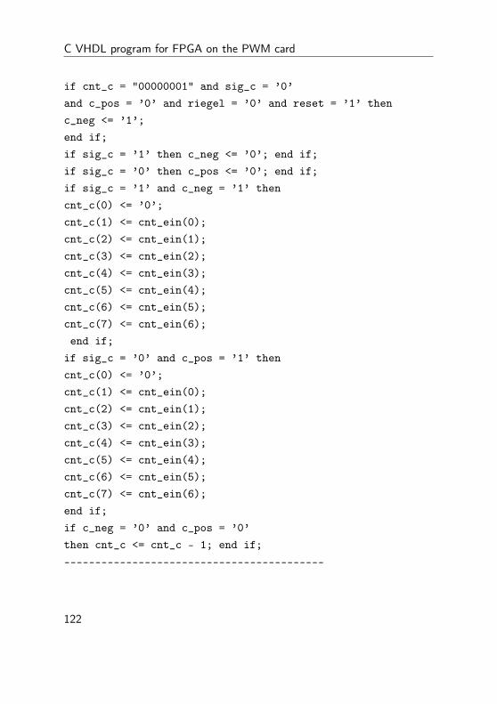
C VHDL program for FPGA on the PWM card
if cnt_c = "00000001" and sig_c = ’0’
and c_pos = ’0’ and riegel = ’0’ and reset = ’1’ then
c_neg <= ’1’;
end if;
if sig_c = ’1’ then c_neg <= ’0’; end if;
if sig_c = ’0’ then c_pos <= ’0’; end if;
if sig_c = ’1’ and c_neg = ’1’ then
cnt_c(0) <= ’0’;
cnt_c(1) <= cnt_ein(0);
cnt_c(2) <= cnt_ein(1);
cnt_c(3) <= cnt_ein(2);
cnt_c(4) <= cnt_ein(3);
cnt_c(5) <= cnt_ein(4);
cnt_c(6) <= cnt_ein(5);
cnt_c(7) <= cnt_ein(6);
end if;
if sig_c = ’0’ and c_pos = ’1’ then
cnt_c(0) <= ’0’;
cnt_c(1) <= cnt_ein(0);
cnt_c(2) <= cnt_ein(1);
cnt_c(3) <= cnt_ein(2);
cnt_c(4) <= cnt_ein(3);
cnt_c(5) <= cnt_ein(4);
cnt_c(6) <= cnt_ein(5);
cnt_c(7) <= cnt_ein(6);
end if;
if c_neg = ’0’ and c_pos = ’0’
then cnt_c <= cnt_c - 1; end if;
------------------------------------------
122

end if;
if (reset = ’0’ or fehler2 = ’0’or PCfrei = ’0’) then
riegel <= ’1’;
end if;
if (tastfrei = ’1’ and reset = ’1’
and fehler2 = ’1’ and PCfrei = ’1’)then
riegel <= ’0’;
end if;
if riegel = ’1’ or reset = ’0’ then
a_pos <= ’0’;
a_neg <= ’0’;
b_pos <= ’0’;
b_neg <= ’0’;
c_pos <= ’0’;
c_neg <= ’0’;
cnt_a(0) <= ’0’;
cnt_a(1) <= cnt_ein(0);
cnt_a(2) <= cnt_ein(1);
cnt_a(3) <= cnt_ein(2);
cnt_a(4) <= cnt_ein(3);
cnt_a(5) <= cnt_ein(4);
cnt_a(6) <= cnt_ein(5);
cnt_a(7) <= cnt_ein(6);
cnt_b(0) <= ’0’;
cnt_b(1) <= cnt_ein(0);
cnt_b(2) <= cnt_ein(1);
cnt_b(3) <= cnt_ein(2);
cnt_b(4) <= cnt_ein(3);
cnt_b(5) <= cnt_ein(4);
123

C VHDL program for FPGA on the PWM card
cnt_b(6) <= cnt_ein(5);
cnt_b(7) <= cnt_ein(6);
cnt_c(0) <= ’0’;
cnt_c(1) <= cnt_ein(0);
cnt_c(2) <= cnt_ein(1);
cnt_c(3) <= cnt_ein(2);
cnt_c(4) <= cnt_ein(3);
cnt_c(5) <= cnt_ein(4);
cnt_c(6) <= cnt_ein(5);
cnt_c(7) <= cnt_ein(6);
end if;
end if;
end process acttod;
end archpwmtod;
124