Embed Size (px)
DESCRIPTION
pxi 6251 specs
Citation preview
NI 625x SpecificationsSpecifications listed below are typical at 25 °C unless otherwise noted. Refer to the M Series User Manual for more information about NI 625x devices.
Analog InputNumber of channels
NI 6250/6251.............................. 8 differential or 16 single ended
NI 6254/6259.............................. 16 differential or 32 single ended
NI 6255....................................... 40 differential or 80 single ended
ADC resolution ............................... 16 bits
DNL ................................................ No missing codes guaranteed
INL.................................................. Refer to the AI Absolute Accuracy Table
Sampling rate
Maximum
NI 6250/6251/6254/6259....... 1.25 MS/s single channel,1.00 MS/s multi-channel (aggregate)
NI 6255 .................................. 1.25 MS/s single channel750 kS/s multi-channel (aggregate)
Minimum.................................... No minimum
Timing accuracy ......................... 50 ppm of sample rate
Timing resolution ....................... 50 ns
Input coupling ................................. DC
Input range ...................................... ±10 V, ±5 V, ±2 V, ±1 V, ±0.5 V, ±0.2 V, ±0.1 V
Maximum working voltage for analog inputs(signal + common mode) ................ ±11 V of AI GND
CMRR (DC to 60 Hz) .....................100 dB
Input impedance
Device on
AI+ to AI GND ......................>10 GΩ in parallel with 100 pF
AI– to AI GND.......................>10 GΩ in parallel with 100 pF
Device off
AI+ to AI GND ......................820 ΩAI– to AI GND.......................820 Ω
Input bias current.............................±100 pA
Crosstalk (at 100 kHz)
Adjacent channels .......................–75 dB
Non-adjacent channels ................–95 dB1
Small signal bandwidth (–3 dB)......1.7 MHz
Input FIFO size................................4,095 samples
Scan list memory .............................4,095 entries
Data transfers
PCI/PCIe/PXI/PXIe devices .......DMA (scatter-gather), interrupts, programmed I/O
USB devices................................USB Signal Stream, programmed I/O
1 For USB-6255 devices, channel AI <0..15> crosstalk to channel AI <64..79> is –67 dB; applies to channels with 64-channel separation, for example, AI (x) and AI (x + 64).
NI 625x Specifications 2 ni.com
Overvoltage protection (AI <0..79>, AI SENSE, AI SENSE 2)
Device on ....................................±25 V for up to four AI pins
Device off ...................................±15 V for up to four AI pins
Input current duringovervoltage condition ......................±20 mA max/AI pin
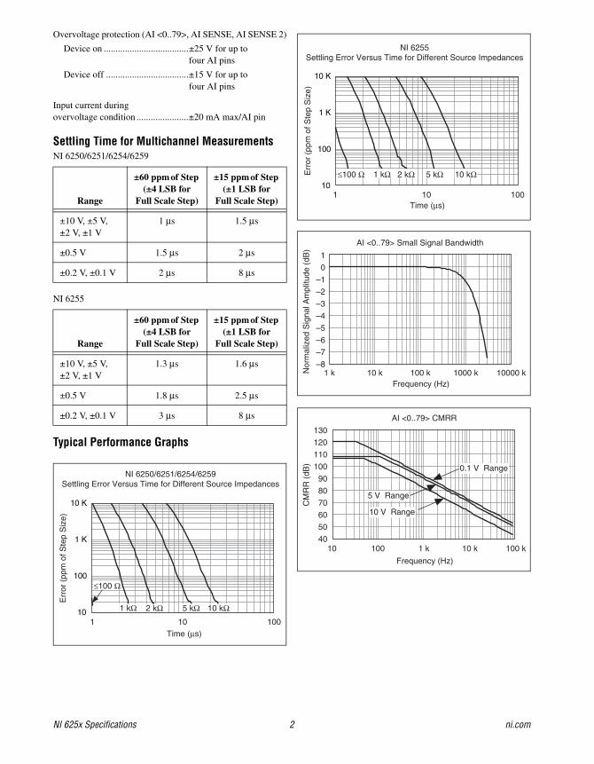
Settling Time for Multichannel MeasurementsNI 6250/6251/6254/6259
NI 6255
Typical Performance Graphs
Range
±60 ppm of Step (±4 LSB for
Full Scale Step)
±15 ppm of Step (±1 LSB for
Full Scale Step)
±10 V, ±5 V, ±2 V, ±1 V
1 μs 1.5 μs
±0.5 V 1.5 μs 2 μs
±0.2 V, ±0.1 V 2 μs 8 μs
Range
±60 ppm of Step (±4 LSB for
Full Scale Step)
±15 ppm of Step (±1 LSB for
Full Scale Step)
±10 V, ±5 V, ±2 V, ±1 V
1.3 μs 1.6 μs
±0.5 V 1.8 μs 2.5 μs
±0.2 V, ±0.1 V 3 μs 8 μs
NI 6250/6251/6254/6259Settling Error Versus Time for Different Source Impedances
1 10 100Time (μs)
Err
or (
ppm
of S
tep
Siz
e)
10
100
1 K
10 K
≤100 Ω
5 kΩ 10 kΩ2 kΩ1 kΩ
NI 6255Settling Error Versus Time for Different Source Impedances
1 10 100Time (μs)
Err
or (
ppm
of S
tep
Siz
e)
10
100
1 K
10 K
5 kΩ 10 kΩ2 kΩ1 kΩ≤100 Ω
AI <0..79> Small Signal Bandwidth
–8
–7
–6
–5
–4
–3
–2
–1
0
1
1 k 10 k 100 k 1000 k 10000 kFrequency (Hz)
Nor
mal
ized
Sig
nal A
mpl
itude
(dB
)
AI <0..79> CMRR
40
50
60
70
80
90
100
110
120
130
10 100 1 k 10 k 100 k
Frequency (Hz)
CM
RR
(dB
)
10 V Range
5 V Range
0.1 V Range
© National Instruments Corporation 3 NI 625x Specifications
Analog TriggersNumber of triggers.......................... 1
Source
NI 6250/6251.............................. AI <0..15>, APFI 0
NI 6254/6259.............................. AI <0..31>, APFI <0..1>
NI 6255....................................... AI <0..79>, APFI 0
Functions......................................... Start Trigger, Reference Trigger, Pause Trigger, Sample Clock, Convert Clock, Sample Clock Timebase
Source level
AI <0..79> .................................. ±full scale
APFI <0..1>................................ ±10 V
Resolution ....................................... 10 bits, 1 in 1,024
Modes.............................................. Analog edge triggering, analog edge triggering with hysteresis, and analog window triggering
Bandwidth (–3 dB)
AI <0..79> .................................. 3.4 MHz
APFI <0..1>................................ 3.9 MHz
Accuracy ......................................... ±1%
APFI <0..1> characteristics
Input impedance ......................... 10 kΩCoupling ..................................... DC
Protection
Power on ................................ ±30 V
Power off................................ ±15 V
Analog OutputNumber of channels
NI 6250/6254 ..............................0
NI 6251/6255 ..............................2
NI 6259 .......................................4
DAC resolution ...............................16 bits
DNL.................................................±1 LSB
Monotonicity ...................................16 bit guaranteed
Accuracy..........................................Refer to the AO Absolute Accuracy Table
Maximum update rate
1 channel .....................................2.86 MS/s
2 channels ...................................2.00 MS/s
3 channels ...................................1.54 MS/s
4 channels ...................................1.25 MS/s
Timing accuracy ..............................50 ppm of sample rate
Timing resolution ............................50 ns
Output range ....................................±10 V, ±5 V, ±external reference on APFI <0..1>
Output coupling...............................DC
Output impedance ...........................0.2 Ω
Output current drive ........................±5 mA
Overdrive protection .......................±25 V
Overdrive current ............................20 mA
Power-on state .................................±5 mV1
Power-on glitch ...............................1.5 V peak for 1.5 s
Output FIFO size .............................8,191 samples shared among channels used
Data transfers
PCI/PCIe/PXI/PXIe devices .......DMA (scatter-gather), interrupts, programmed I/O
USB devices................................USB Signal Stream, programmed I/O
1 For all USB-6251/6259 Screw Terminal devices, when powered on, the analog output signal is not defined until after USB configuration is complete.
NI 625x Specifications 4 ni.com
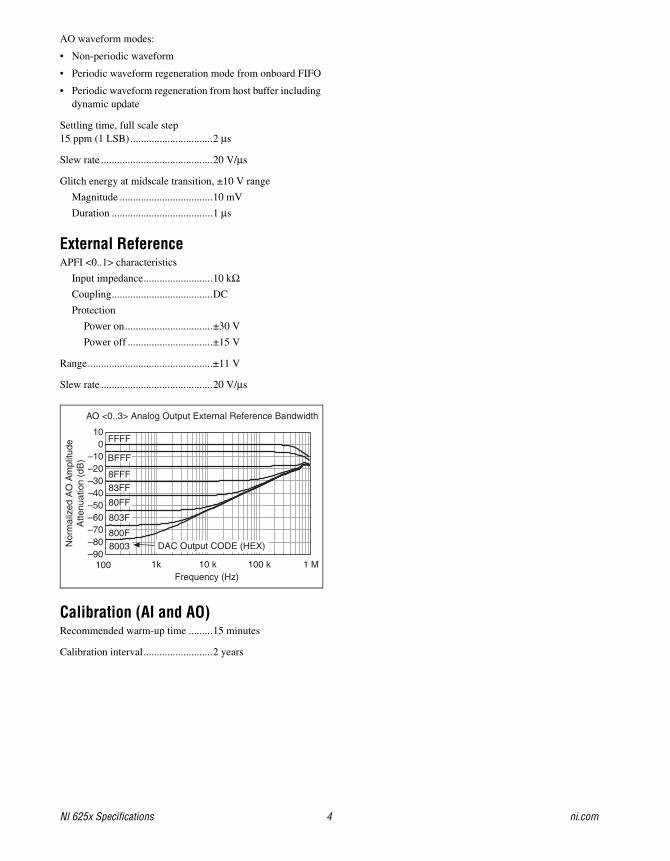
AO waveform modes:
• Non-periodic waveform
• Periodic waveform regeneration mode from onboard FIFO
• Periodic waveform regeneration from host buffer including dynamic update
Settling time, full scale step15 ppm (1 LSB)...............................2 μs
Slew rate ..........................................20 V/μs
Glitch energy at midscale transition, ±10 V range
Magnitude ...................................10 mV
Duration ......................................1 μs
External ReferenceAPFI <0..1> characteristics
Input impedance..........................10 kΩCoupling......................................DC
Protection
Power on.................................±30 V
Power off ................................±15 V
Range...............................................±11 V
Slew rate ..........................................20 V/μs
Calibration (AI and AO)Recommended warm-up time .........15 minutes
Calibration interval..........................2 years
AO <0..3> Analog Output External Reference Bandwidth
–90–80–70–60–50–40–30–20–10
010
100 1k 10 k 100 k 1 MFrequency (Hz)
Nor
mal
ized
AO
Am
plitu
deA
ttenu
atio
n (d
B)
DAC Output CODE (HEX)8003800F
803F
80FF
83FF
8FFF
BFFF
FFFF
© National Instruments Corporation 5 NI 625x Specifications
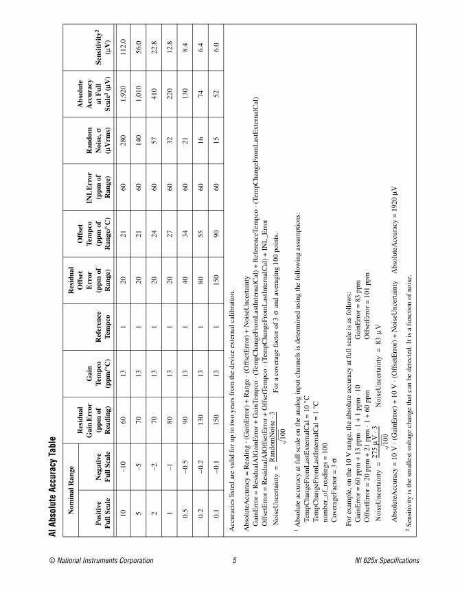
AI A
bsol
ute
Accu
racy
Tab
le
Nom
inal
Ran
geR
esid
ual
Gai
n E
rror
(p
pm o
f R
eadi
ng)
Gai
n Te
mpc
o (p
pm/°
C)
Ref
eren
ce
Tem
pco
Res
idua
l O
ffse
t E
rror
(p
pmof
R
ange
)
Off
set
Tem
pco
(ppm
of
Ran
ge/°
C)
INL
Err
or
(ppm
of
Ran
ge)
Ran
dom
N
oise
, σ
(μV
rms)
Abs
olut
e A
ccur
acy
at F
ull
Scal
e1 (μ
V)
Sens
itiv
ity2
(μV
)P
osit
ive
Ful
lSca
leN
egat
ive
Ful
lSca
le
10–1
060
131
2021
6028
01,
920
112.
0
5–5
7013
120
2160
140
1,01
056
.0
2–2
7013
120
2460
5741
022
.8
1–1
8013
120
2760
3222
012
.8
0.5
–0.
590
131
4034
6021
130
8.4
0.2
–0.
213
013
180
5560
1674
6.4
0.1
–0.
115
013
115
090
6015
526.
0
Acc
urac
ies
list
ed a
re v
alid
for
up
to tw
o ye
ars
from
the
devi
ce e
xter
nal c
alib
ratio
n.
Abs
olut
eAcc
urac
y =
Rea
ding
· (G
ainE
rror
) +
Ran
ge ·
(Off
setE
rror
) +
Noi
seU
ncer
tain
tyG
ainE
rror
= R
esid
ualA
IGai
nErr
or +
Gai
nTem
pco
· (Te
mpC
hang
eFro
mL
astI
nter
nalC
al)
+ R
efer
ence
Tem
pco
· (Te
mpC
hang
eFro
mL
astE
xter
nalC
al)
Off
setE
rror
= R
esid
ualA
IOff
setE
rror
+ O
ffse
tTem
pco
· (Te
mpC
hang
eFro
mL
astI
nter
nalC
al)
+ I
NL
_Err
or
1 A
bsol
ute
accu
racy
at f
ull s
cale
on
the
anal
og in
put c
hann
els
is d
eter
min
ed u
sing
the
foll
owin
g as
sum
ptio
ns:
Tem
pCha
ngeF
rom
Las
tExt
erna
lCal
= 1
0°C
Tem
pCha
ngeF
rom
Las
tInt
erna
lCal
= 1
°Cnu
mbe
r_of
_rea
ding
s =
100
Cov
erag
eFac
tor
= 3
σ
For
exam
ple,
on
the
10 V
ran
ge, t
he a
bsol
ute
accu
racy
at f
ull s
cale
is a
s fo
llow
s:G
ainE
rror
= 6
0 pp
m +
13
ppm
· 1
+ 1
ppm
· 10
Gai
nErr
or =
83
ppm
Off
setE
rror
= 2
0 pp
m +
21
ppm
· 1
+ 6
0pp
mO
ffse
tErr
or =
101
ppm
Abs
olut
eAcc
urac
y =
10
V ·
(Gai
nErr
or)
+ 1
0 V
· (O
ffse
tErr
or)
+ N
oise
Unc
erta
inty
Abs
olut
eAcc
urac
y =
192
0 μV
2 Se
nsiti
vity
is th
e sm
alle
st v
olta
ge c
hang
e th
at c
an b
e de
tect
ed. I
t is
a fu
nctio
n of
noi
se.
Noi
seU
ncer
tain
tyR
ando
mN
oise
3⋅10
0----
--------
--------
--------
--------
-----
=Fo
r a c
over
age
fact
or o
f 3 σ
and
ave
ragi
ng 1
00 p
oint
s.
Noi
seU
ncer
tain
ty27
5 μ
V3⋅
100
--------
--------
--------
--=
Noi
seU
ncer
tain
ty83
μV
=
NI 625x Specifications 6 ni.com
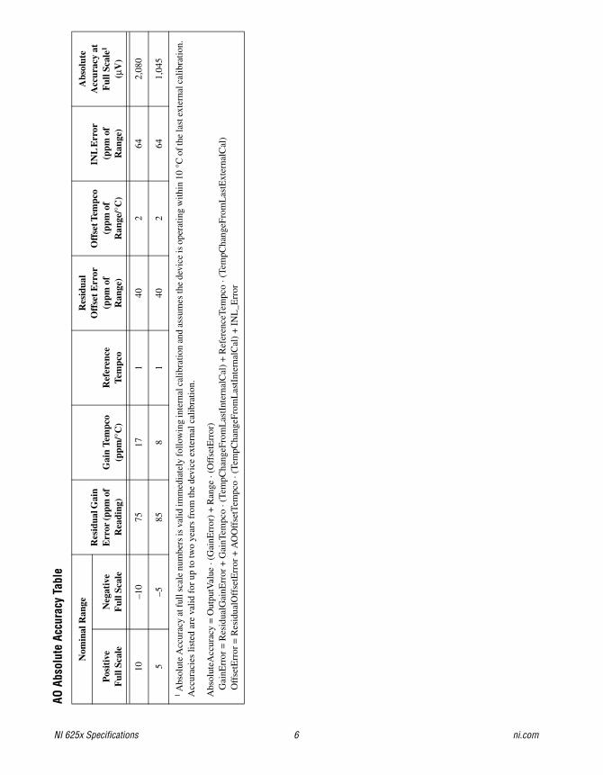
AO A
bsol
ute
Accu
racy
Tab
le
Nom
inal
Ran
geR
esid
ual G
ain
Err
or (p
pm o
f R
eadi
ng)
Gai
n T
empc
o (p
pm/°
C)
Ref
eren
ce
Tem
pco
Res
idua
l O
ffse
t E
rror
(p
pmof
R
ange
)
Off
set T
empc
o (p
pm o
f R
ange
/°C
)
INL
Err
or
(p
pmof
R
ange
)
Abs
olut
e A
ccur
acy
at
Ful
l Sca
le1
(μV
)P
osit
ive
Ful
lSca
leN
egat
ive
Ful
lSca
le
10–1
075
171
402
642,
080
5–5
858
140
264
1,04
5
1 A
bsol
ute
Acc
urac
y at
full
scal
e nu
mbe
rs is
val
id im
med
iate
ly fo
llow
ing
inte
rnal
cal
ibra
tion
and
assu
mes
the
devi
ce is
ope
ratin
g w
ithin
10
°C o
f the
last
ext
erna
l cal
ibra
tion.
A
ccur
acie
s li
sted
are
val
id f
or u
p to
two
year
s fr
om th
e de
vice
ext
erna
l cal
ibra
tion.
Abs
olut
eAcc
urac
y =
Out
putV
alue
· (G
ainE
rror
) +
Ran
ge ·
(Off
setE
rror
)G
ainE
rror
= R
esid
ualG
ainE
rror
+ G
ainT
empc
o · (
Tem
pCha
ngeF
rom
Las
tInt
erna
lCal
) +
Ref
eren
ceTe
mpc
o · (
Tem
pCha
ngeF
rom
Las
tExt
erna
lCal
)O
ffse
tErr
or =
Res
idua
lOff
setE
rror
+ A
OO
ffse
tTem
pco
· (Te
mpC
hang
eFro
mL
astI
nter
nalC
al)
+ I
NL
_Err
or
© National Instruments Corporation 7 NI 625x Specifications
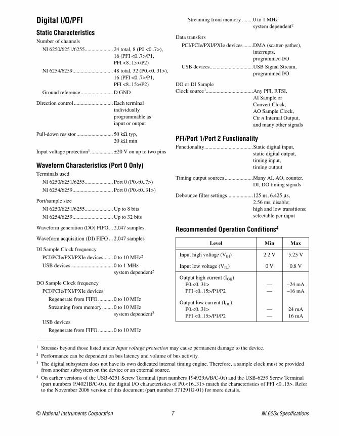
Digital I/O/PFIStatic CharacteristicsNumber of channels
NI 6250/6251/6255..................... 24 total, 8 (P0.<0..7>), 16 (PFI <0..7>/P1, PFI <8..15>/P2)
NI 6254/6259.............................. 48 total, 32 (P0.<0..31>), 16 (PFI <0..7>/P1, PFI <8..15>/P2)
Ground reference........................ D GND
Direction control ............................. Each terminal individually programmable as input or output
Pull-down resistor ........................... 50 kΩ typ,20 kΩ min
Input voltage protection1................. ±20 V on up to two pins
Waveform Characteristics (Port 0 Only)Terminals used
NI 6250/6251/6255..................... Port 0 (P0.<0..7>)
NI 6254/6259.............................. Port 0 (P0.<0..31>)
Port/sample size
NI 6250/6251/6255..................... Up to 8 bits
NI 6254/6259.............................. Up to 32 bits
Waveform generation (DO) FIFO ... 2,047 samples
Waveform acquisition (DI) FIFO ... 2,047 samples
DI Sample Clock frequency
PCI/PCIe/PXI/PXIe devices....... 0 to 10 MHz2
USB devices ............................... 0 to 1 MHz system dependent2
DO Sample Clock frequency
PCI/PCIe/PXI/PXIe devices
Regenerate from FIFO ........... 0 to 10 MHz
Streaming from memory........ 0 to 10 MHz system dependent2
USB devices
Regenerate from FIFO ........... 0 to 10 MHz
Streaming from memory ........0 to 1 MHz system dependent2
Data transfers
PCI/PCIe/PXI/PXIe devices .......DMA (scatter-gather), interrupts, programmed I/O
USB devices................................USB Signal Stream, programmed I/O
DO or DI SampleClock source3...................................Any PFI, RTSI,
AI Sample or Convert Clock, AO Sample Clock, Ctr n Internal Output, and many other signals
PFI/Port 1/Port 2 FunctionalityFunctionality....................................Static digital input,
static digital output,timing input,timing output
Timing output sources .....................Many AI, AO, counter, DI, DO timing signals
Debounce filter settings...................125 ns, 6.425 μs, 2.56 ms, disable; high and low transitions; selectable per input
Recommended Operation Conditions4
1 Stresses beyond those listed under Input voltage protection may cause permanent damage to the device.2 Performance can be dependent on bus latency and volume of bus activity.3 The digital subsystem does not have its own dedicated internal timing engine. Therefore, a sample clock must be provided
from another subsystem on the device or an external source.4 On earlier versions of the USB-6251 Screw Terminal (part numbers 194929A/B/C-0x) and the USB-6259 Screw Terminal
(part numbers 194021B/C-0x), the digital I/O characteristics of P0.<16..31> match the characteristics of PFI <0..15>. Refer to the November 2006 version of this document (part number 371291G-01) for more details.
Level Min Max
Input high voltage (VIH) 2.2 V 5.25 V
Input low voltage (VIL) 0 V 0.8 V
Output high current (IOH)P0.<0..31>PFI <0..15>/P1/P2
——
–24 mA–16 mA
Output low current (IOL)P0.<0..31>PFI <0..15>/P1/P2
——
24 mA16 mA
NI 625x Specifications 8 ni.com
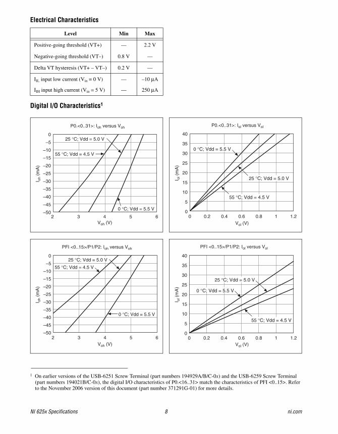
Electrical Characteristics
Digital I/O Characteristics1
Level Min Max
Positive-going threshold (VT+) — 2.2 V
Negative-going threshold (VT–) 0.8 V —
Delta VT hysteresis (VT+ – VT–) 0.2 V —
IIL input low current (Vin = 0 V)
IIH input high current (Vin = 5 V)
—
—
–10 μA
250 μA
1 On earlier versions of the USB-6251 Screw Terminal (part numbers 194929A/B/C-0x) and the USB-6259 Screw Terminal (part numbers 194021B/C-0x), the digital I/O characteristics of P0.<16..31> match the characteristics of PFI <0..15>. Refer to the November 2006 version of this document (part number 371291G-01) for more details.
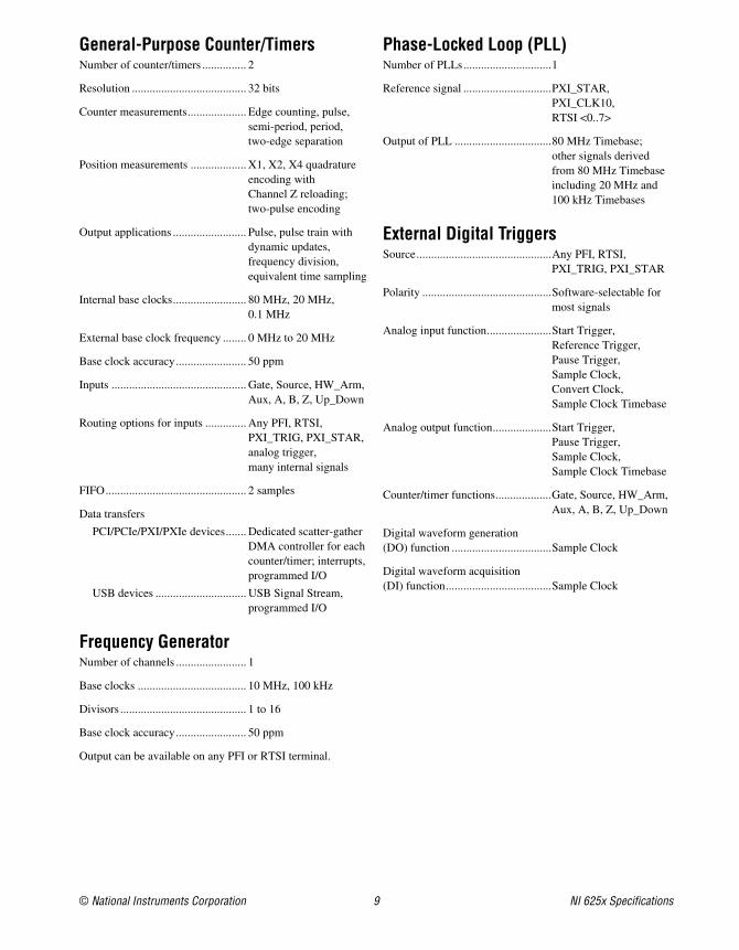
–50
–45
–40
–35
–30
–25
–20
–15
–10
–5
0
2 3 4 5 6Voh (V)
I oh
(mA
)
0 °C; Vdd = 5.5 V
55 °C; Vdd = 4.5 V
25 °C; Vdd = 5.0 V
P0.<0..31>: Ioh versus Voh
–50
–45
–40
–35
–30
–25
–20
–15
–10
–5
0
2 3 4 5 6Voh (V)
I oh
(mA
)
PFI <0..15>/P1/P2: Ioh versus Voh
0 °C; Vdd = 5.5 V
55 °C; Vdd = 4.5 V
25 °C; Vdd = 5.0 V
0
5
10
15
20
25
30
35
40
0 0.2 0.4 0.6 0.8 1 1.2Vol (V)
I ol (
mA
)
P0.<0..31>: Iol versus Vol
0 °C; Vdd = 5.5 V
55 °C; Vdd = 4.5 V
25 °C; Vdd = 5.0 V
0
5
10
15
20
25
30
35
40
0 0.2 0.4 0.6 0.8 1 1.2Vol (V)
I ol (
mA
)
PFI <0..15>/P1/P2: Iol versus Vol
0 °C; Vdd = 5.5 V
55 °C; Vdd = 4.5 V
25 °C; Vdd = 5.0 V
© National Instruments Corporation 9 NI 625x Specifications
General-Purpose Counter/TimersNumber of counter/timers ............... 2
Resolution ....................................... 32 bits
Counter measurements.................... Edge counting, pulse, semi-period, period, two-edge separation
Position measurements ................... X1, X2, X4 quadrature encoding with Channel Z reloading; two-pulse encoding
Output applications ......................... Pulse, pulse train with dynamic updates, frequency division, equivalent time sampling
Internal base clocks......................... 80 MHz, 20 MHz, 0.1 MHz
External base clock frequency ........ 0 MHz to 20 MHz
Base clock accuracy........................ 50 ppm
Inputs .............................................. Gate, Source, HW_Arm, Aux, A, B, Z, Up_Down
Routing options for inputs .............. Any PFI, RTSI, PXI_TRIG, PXI_STAR, analog trigger, many internal signals
FIFO................................................ 2 samples
Data transfers
PCI/PCIe/PXI/PXIe devices....... Dedicated scatter-gather DMA controller for each counter/timer; interrupts, programmed I/O
USB devices ............................... USB Signal Stream, programmed I/O
Frequency GeneratorNumber of channels ........................ 1
Base clocks ..................................... 10 MHz, 100 kHz
Divisors ........................................... 1 to 16
Base clock accuracy........................ 50 ppm
Output can be available on any PFI or RTSI terminal.
Phase-Locked Loop (PLL)Number of PLLs..............................1
Reference signal ..............................PXI_STAR, PXI_CLK10, RTSI <0..7>
Output of PLL .................................80 MHz Timebase; other signals derived from 80 MHz Timebase including 20 MHz and 100 kHz Timebases
External Digital TriggersSource..............................................Any PFI, RTSI,
PXI_TRIG, PXI_STAR
Polarity ............................................Software-selectable for most signals
Analog input function......................Start Trigger, Reference Trigger, Pause Trigger, Sample Clock, Convert Clock, Sample Clock Timebase
Analog output function....................Start Trigger, Pause Trigger, Sample Clock, Sample Clock Timebase
Counter/timer functions...................Gate, Source, HW_Arm, Aux, A, B, Z, Up_Down
Digital waveform generation(DO) function ..................................Sample Clock
Digital waveform acquisition(DI) function....................................Sample Clock
NI 625x Specifications 10 ni.com
Device-To-Device Trigger BusPCI/PCIe devices.............................RTSI <0..7>1
PXI/PXIe devices ............................PXI_TRIG <0..7>, PXI_STAR
USB devices ....................................None
Output selections .............................10 MHz Clock; frequency generator output; many internal signals
Debounce filter settings...................125 ns, 6.425 μs, 2.56 ms, disable; high and low transitions; selectable per input
Bus InterfacePCI/PXI devices ..............................3.3 V or 5 V signal
environment
PCIe devices
Form factor .................................x1 PCI Express, specification v1.0a compliant
Slot compatibility........................x1, x4, x8, and x16 PCI Express slots2
PXIe devices
Form factor .................................x1 PXI Express peripheral module, specification rev 1.0 compliant
Slot compatibility........................x1 and x4 PXI Express or PXI Express hybrid slots
USB devices ....................................USB 2.0 Hi-Speed or full-speed3,4
DMA channels(PCI/PCIe/PXI/PXIe devices) .........6, analog input,
analog output, digital input, digital output, counter/timer 0, counter/timer 1
USB Signal Stream (USB devices) ................................. 4, can be used for analog
input, analog output, digital input, digital output, counter/timer 0, counter/timer 1
All PXI-625x devices support one of the following features:
• May be installed in PXI Express hybrid slots
• Or, may be used to control SCXI in PXI/SCXI combo chassis
All NI PXIe-625x devices may be installed in PXI Express slots or PXI Express hybrid slots.
1 In other sections of this document, RTSI refers to RTSI <0..7> for PCI/PCIe devices or PXI_TRIG <0..7> for PXI/PXIe devices.
2 Some motherboards reserve the x16 slot for graphics use. For PCI Express guidelines, refer to ni.com/pciexpress.3 If you are using a USB M Series device in full-speed mode, device performance will be lower and you will not be able to
achieve maximum sampling/update rates.4 Operating on a full-speed bus may result in lower high-speed full-speed performance.
Table 1. PXI/SCXI Combo and PXI Express Chassis Compatibility
M Series Device
M Series Part Number
SCXI Control in PXI/SCXI
Combo Chassis
PXI Express
Hybrid Slot Compatible
PXI-6250 191325D-04/191325E-04L
No Yes
PXI-6251 191325D-03/191325E-03L
No Yes
191325D-13/191325E-13L
Yes No
PXI-6254 191325D-02/191325E-03L
No Yes
PXI-6255 193618A-01 No Yes
PXI-6259 191325D-01/191325E-01L
No Yes
191325D-11/191325E-11L
Yes No
Earlier versions of PXI-6251/ 6254/6259
191325C-0x191325B-0x
Yes No
© National Instruments Corporation 11 NI 625x Specifications
Power RequirementsCurrent draw from bus during no-load condition1
PCI/PXI devices
+5 V ....................................... 0.03 A
+3.3 V .................................... 0.725 A
+12 V ..................................... 0.35 A
PCIe devices
+3.3 V .................................... 0.925 A
+12 V ..................................... 0.35 A
PXIe devices
+3.3 V .................................... 0.45 A
+12 V ..................................... 0.5 A
Current draw from bus during AI and AO overvoltage condition2
PCI/PXI devices
+5 V ....................................... 0.03 A
+3.3 V .................................... 1.2 A
+12 V ..................................... 0.38 A
PCIe devices
+3.3 V .................................... 1.4 A
+12 V ..................................... 0.38 A
PXIe devices
+3.3 V .................................... 0.48 A
+12 V ..................................... 0.71 A
Caution USB-625x devices must be powered with NI offered AC adapter or a National Electric Code (NEC) Class 2 DC source that meets the power requirements for the device and has appropriate safety certification marks for country of use.
USB power supply requirements .... 11 to 30 VDC, 20 W, locking or non-locking power jack with 0.080” diameter center pin, 5/16–32 thread for locking collars
Power Limits
Caution Exceeding the power limits may cause unpredictable behavior by the device and/or PC/chassis.
PCI devices
+5 V terminal (connector 0)........1 A max3
+5 V terminal (connector 1)........1 A max3
PCIe devices
Without disk drive power connector installed
+5 V terminals combined .......0.35 A max3
P0/PFI/P1/P2 and +5 V terminals combined ................0.39 A max
With disk drive power connector installed
+5 V terminal (connector 0) ...1 A max3
+5 V terminal (connector 1) ...1 A max3
P0/PFI/P1/P2 combined .........0.39 A max
PXI/PXIe devices
+5 V terminal (connector 0)........1 A max3
+5 V terminal (connector 1)........1 A max3
P0/PFI/P1/P2 and +5 V terminals combined.....................2 A max
USB devices
+5 V terminal ..............................1 A max3
P0/PFI/P1/P2 and +5 V terminals combined.....................2 A max
Power supply fuse.......................2 A, 250 V
Physical RequirementsPrinted circuit board dimensions
NI PCI-6250/6251/6254/6255/6259 ...................................9.7 × 15.5 cm
(3.8 × 6.1 in.)
NI PCIe-6251/6259.....................9.9 × 16.8 cm (3.9 × 6.6 in.) (half-length)
NI PXI/PXIe-6250/6251/6254/6255/6259 ..........................Standard 3U PXI
1 Does not include P0/PFI/P1/P2 and +5 V terminals.2 Does not include P0/PFI/P1/P2 and +5 V terminals.3 Has a self-resetting fuse that opens when current exceeds this specification.
NI 625x Specifications 12 ni.com
Enclosure dimensions (includes connectors)
NI USB-6251/6255/6259 Screw Terminal...........................26.67 × 17.09 × 4.45 cm
(10.5 × 6.73 × 1.75 in.)
NI USB-6251/6259 BNC............28.6 × 17 × 6.9 cm (11.25 × 6.7 × 2.7 in.)
NI USB-6251/6255/6259Mass Termination .......................18.8 × 17.09 × 4.45 cm
(7.4 × 6.73 × 1.75 in.)
NI USB-6251/6255/6259OEM............................................Refer to the
NI USB-622x/625x OEM User Guide
Weight
NI PCI-6250................................142 g (5 oz)
NI PCI-6251................................149 g (5.2 oz)
NI PCI-6254................................152 g (5.3 oz)
NI PCI-6255................................164 g (5.8 oz)
NI PCI-6259................................162 g (5.6 oz)
NI PCIe-6251..............................161 g (5.7 oz)
NI PCIe-6259..............................175 g (6.1 oz)
NI PXI-6250 ...............................212 g (7.5 oz)
NI PXI-6251/6254 ......................222 g (7.8 oz)
NI PXI-6255 ...............................236 g (8.3 oz)
NI PXI-6259 ...............................233 g (8.2 oz)
NI PXIe-6251..............................208 g (7.3 oz)
NI PXIe-6259..............................221 g (7.8 oz)
NI USB-6251 Screw Terminal ...1.2 kg (2 lb 10 oz)
NI USB-6255/6259 Screw Terminal...........................1.24 kg (2 lb 11 oz)
NI USB-6251/6255/6259Mass Termination .......................816 g (1 lb 12.8 oz)
NI USB-6251 OEM ....................140 g (4.9 oz)
NI USB-6255/6259 OEM ...........172 g (6.1 oz)
I/O connector
NI PCI/PCIe/PXI/PXIe-6250/6251............................................ 1 68-pin VHDCI
NI PCI/PCIe/PXI/PXIe-6254/6255/6259................................... 2 68-pin VHDCI
NI USB-6251 Screw Terminal ... 64 screw terminals
NI USB-6255/6259 Screw Terminal .......................... 128 screw terminals
NI USB-6251 BNC .................... 21 BNCs and 30 screw terminals
NI USB-6259 BNC .................... 32 BNCs and 60 screw terminals
NI USB-6251Mass Termination....................... 1 68-pin SCSI
NI USB-6255/6259 Mass Termination....................... 2 68-pin SCSI
Disk drive power connector (PCIe devices)................................. Standard ATX
peripheral connector (not serial ATA)
USB-6251/6255/6259 Screw Terminal/USB-6251/6259 BNCscrew terminal wiring ..................... 16–28 AWG
Maximum Working Voltage1
NI 6250/6251/6254/6255/6259Channel-to-earth ............................. 11 V,
Measurement Category I
Caution Do not use for measurements within Categories II, III, or IV.
EnvironmentalOperating temperature
PCI/PXI/PXIe devices................ 0 to 55 °C
PCIe devices ............................... 0 to 50 °C
USB devices ............................... 0 to 45 °C
Storage temperature ........................ –20 to 70 °C
Humidity ......................................... 10 to 90% RH, noncondensing
Maximum altitude........................... 2,000 m
Pollution Degree(indoor use only) ............................. 2
1 Maximum working voltage refers to the signal voltage plus the common-mode voltage.
© National Instruments Corporation 13 NI 625x Specifications
Shock and Vibration (PXI/PXIe Devices Only)Operational shock ........................... 30 g peak, half-sine,
11 ms pulse (Tested in accordance with IEC-60068-2-27. Test profile developed in accordance with MIL-PRF-28800F.)
Random vibration
Operating .................................... 5 to 500 Hz, 0.3 grms
Nonoperating .............................. 5 to 500 Hz, 2.4 grms (Tested in accordance with IEC-60068-2-64. Nonoperating test profile exceeds the requirements of MIL-PRF-28800F, Class 3.)
SafetyThis product is designed to meet the requirements of the following standards of safety for electrical equipment for measurement, control, and laboratory use:
• IEC 61010-1, EN 61010-1
• UL 61010-1, CSA 61010-1
Note For UL and other safety certifications, refer to the product label or visit ni.com/certification, search by model number or product line, and click the appropriate link in the Certification column.
Electromagnetic CompatibilityThis product is designed to meet the requirements of the following standards of EMC for electrical equipment for measurement, control, and laboratory use:
• EN 61326 EMC requirements; Minimum Immunity
• EN 55011 Emissions; Group 1, Class A
• CE, C-Tick, ICES, and FCC Part 15 Emissions; Class A
Note For EMC compliance, operate this device according to product documentation.
CE ComplianceThis product meets the essential requirements of applicable European Directives, as amended for CE marking, as follows:
• 73/23/EEC; Low-Voltage Directive (safety)
• 89/336/EEC; Electromagnetic Compatibility Directive (EMC)
Note Refer to the Declaration of Conformity (DoC) for this product for any additional regulatory compliance information. To obtain the DoC for this product, visit ni.com/certification, search by model number or product line, and click the appropriate link in the Certification column.
Environmental ManagementNational Instruments is committed to designing and manufacturing products in an environmentally responsible manner. NI recognizes that eliminating certain hazardous substances from our products is beneficial not only to the environment but also to NI customers.
For additional environmental information, refer to the NI and the Environment Web page at ni.com/environment. This page contains the environmental regulations and directives with which NI complies, as well as any other environmental information not included in this document.
Waste Electrical and Electronic Equipment (WEEE)EU Customers At the end of their life cycle, all products must be sent to a WEEE recycling center. For more information about WEEE recycling centers and National Instruments WEEE initiatives, visit ni.com/environment/weee.htm.
RoHSNational Instruments
(RoHS)National Instruments RoHS
ni.com/environment/rohs_china(For information about China RoHS compliance, go to ni.com/environment/rohs_china.)
NI 625x Specifications 14 ni.com
Figure 1. NI PCI/PXI-6250 Pinout
CO
NN
EC
TOR
0(A
I 0-1
5)
D GND
D GND
PFI 8/P2.0
PFI 7/P1.7
PFI 15/P2.7
PFI 13/P2.5
PFI 4/P1.4
PFI 3/P1.3
PFI 2/P1.2
D GND
PFI 10/P2.2
PFI 11/P2.3
P0.3
P0.7
P0.2
D GND
P0.5
P0.0
D GND
NC
NC
AI GND
AI 7
AI 14
AI GND
AI 5
AI 12
AI SENSE
AI 11
AI GND
AI 2
AI 9
AI GND
AI 0
PFI 14/P2.6
PFI 9/P2.1
D GND
PFI 5/P1.5
D GND
+5 V
D GND
PFI 12/P2.4
PFI 6/P1.6
PFI 1/P1.1
PFI 0/P1.0
D GND
D GND
+5 V
D GND
P0.6
P0.1
D GND
P0.4
APFI 0
NC
NC
AI 15
AI GND
AI 6
AI 13
AI GND
AI 4
AI GND
AI 3
AI 10
AI GND
AI 1
AI 868 34
67 33
66 32
65 31
64 30
63 29
62 28
61 27
60 26
59 25
58 24
57 23
56 22
55 21
54 20
53 19
52 18
51 17
50 16
49 15
48 14
47 13
46 12
45 11
44 10
43 9
42 8
41 7
40 6
39 5
38 4
37 3
36 2
35 1
TERMINAL 34TERMINAL 68
TERMINAL 1TERMINAL 35
NC = No Connect
© National Instruments Corporation 15 NI 625x Specifications
Figure 2. NI PCI/PCIe/PXI/PXIe-6251 Pinout
CO
NN
EC
TOR
0(A
I 0-1
5)
D GND
D GND
PFI 8/P2.0
PFI 7/P1.7
PFI 15/P2.7
PFI 13/P2.5
PFI 4/P1.4
PFI 3/P1.3
PFI 2/P1.2
D GND
PFI 10/P2.2
PFI 11/P2.3
P0.3
P0.7
P0.2
D GND
P0.5
P0.0
D GND
AO GND
AO GND
AI GND
AI 7
AI 14
AI GND
AI 5
AI 12
AI SENSE
AI 11
AI GND
AI 2
AI 9
AI GND
AI 0
PFI 14/P2.6
PFI 9/P2.1
D GND
PFI 5/P1.5
D GND
+5 V
D GND
PFI 12/P2.4
PFI 6/P1.6
PFI 1/P1.1
PFI 0/P1.0
D GND
D GND
+5 V
D GND
P0.6
P0.1
D GND
P0.4
APFI 0
AO 1
AO 0
AI 15
AI GND
AI 6
AI 13
AI GND
AI 4
AI GND
AI 3
AI 10
AI GND
AI 1
AI 868 34
67 33
66 32
65 31
64 30
63 29
62 28
61 27
60 26
59 25
58 24
57 23
56 22
55 21
54 20
53 19
52 18
51 17
50 16
49 15
48 14
47 13
46 12
45 11
44 10
43 9
42 8
41 7
40 6
39 5
38 4
37 3
36 2
35 1
TERMINAL 34TERMINAL 68
TERMINAL 1TERMINAL 35
NI 625x Specifications 16 ni.com
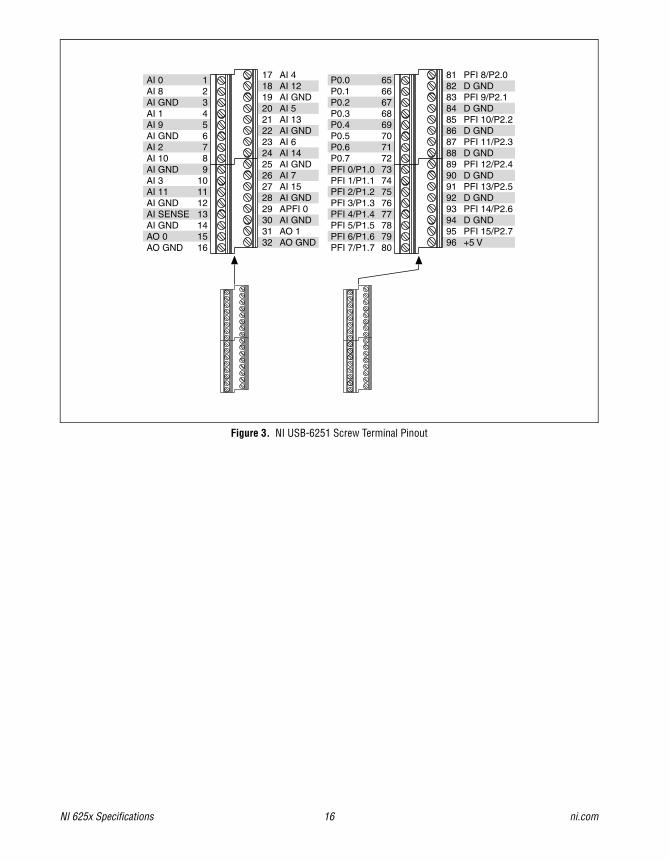
Figure 3. NI USB-6251 Screw Terminal Pinout
17181920212223242526272829303132
AI 4AI 12AI GNDAI 5AI 13AI GNDAI 6AI 14AI GNDAI 7AI 15AI GNDAPFI 0AI GNDAO 1AO GND
AI 0AI 8AI GNDAI 1AI 9AI GNDAI 2AI 10AI GNDAI 3AI 11AI GNDAI SENSEAI GNDAO 0AO GND
123456789
10111213141516
81828384858687888990919293949596
PFI 8/P2.0D GNDPFI 9/P2.1D GNDPFI 10/P2.2D GNDPFI 11/P2.3D GNDPFI 12/P2.4D GNDPFI 13/P2.5D GNDPFI 14/P2.6D GNDPFI 15/P2.7+5 V
P0.0P0.1P0.2P0.3P0.4P0.5P0.6P0.7PFI 0/P1.0PFI 1/P1.1PFI 2/P1.2PFI 3/P1.3PFI 4/P1.4PFI 5/P1.5PFI 6/P1.6PFI 7/P1.7
65666768697071727374757677787980
© National Instruments Corporation 17 NI 625x Specifications
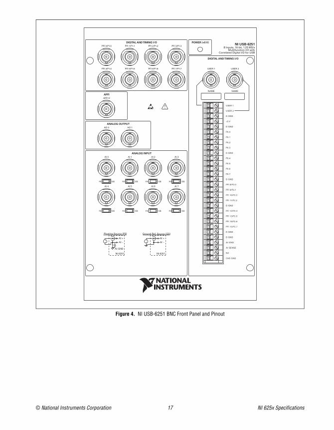
Figure 4. NI USB-6251 BNC Front Panel and Pinout
NI 625x Specifications 18 ni.com
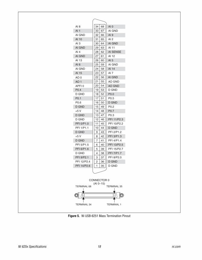
Figure 5. NI USB-6251 Mass Termination Pinout
PFI 14/P2.6
PFI 12/P2.4
PFI 9/P2.1
D GND
PFI 6/P1.6
PFI 5/P1.5
D GND
+5 V
D GND
PFI 1/P1.1
PFI 0/P1.0
D GND
D GND
+5 V
D GND
P0.6
P0.1
D GND
P0.4APFI 0
AO 1
AO 0
AI 15
AI GND
AI 6
AI 13
AI GND
AI 4
AI GND
AI 3
AI 10
AI GND
AI 1
AI 8
D GND
PFI 8/P2.0
PFI 7/P1.7
PFI 13/P2.5
PFI 4/P1.4
PFI 3/P1.3
PFI 2/P1.2
D GND
PFI 15/P2.7
D GND
PFI 10/P2.2
PFI 11/P2.3
P0.3
P0.7
P0.2
D GND
P0.5
P0.0
D GNDAO GND
AO GND
AI GND
AI 7
AI 14
AI GND
AI 5
AI 12
AI SENSE
AI 11
AI GND
AI 2
AI 9
AI GND
AI 0
1
2
3
4
5
6
7
8
9
10
11
12
13
14
15
16
17
18
19
20
21
22
23
24
25
26
27
28
29
30
31
32
33
34
35
36
37
38
39
40
41
42
43
44
45
46
47
48
49
50
51
52
53
54
55
56
57
58
59
60
61
62
63
64
65
66
67
68
CONNECTOR 0(AI 0–15)
TERMINAL 34
TERMINAL 68
TERMINAL 1
TERMINAL 35
© National Instruments Corporation 19 NI 625x Specifications
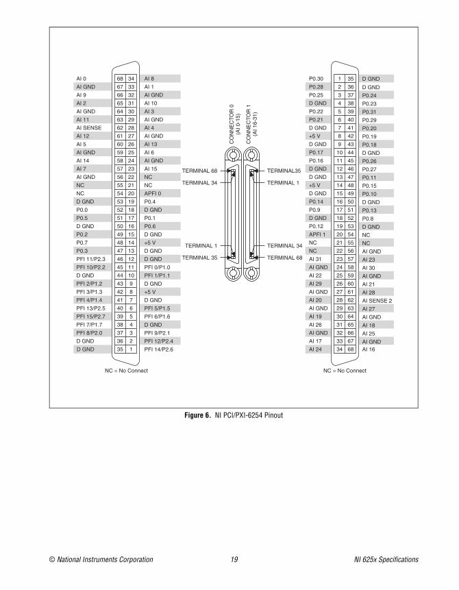
Figure 6. NI PCI/PXI-6254 Pinout
CO
NN
EC
TOR
0(A
I 0-1
5)
CO
NN
EC
TOR
1(A
I 16-
31)
D GND
D GND
PFI 8/P2.0
PFI 7/P1.7
PFI 15/P2.7
PFI 13/P2.5
PFI 4/P1.4
PFI 3/P1.3
PFI 2/P1.2
D GND
PFI 10/P2.2
PFI 11/P2.3
P0.3
P0.7
P0.2
D GND
P0.5
P0.0
D GND
NC
NC
AI GND
AI 7
AI 14
AI GND
AI 5
AI 12
AI SENSE
AI 11
AI GND
AI 2
AI 9
AI GND
AI 0
PFI 14/P2.6
PFI 9/P2.1
D GND
PFI 5/P1.5
D GND
+5 V
D GND
PFI 12/P2.4
PFI 6/P1.6
PFI 1/P1.1
PFI 0/P1.0
D GND
D GND
+5 V
D GND
P0.6
P0.1
D GND
P0.4
APFI 0
NC
NC
AI 15
AI GND
AI 6
AI 13
AI GND
AI 4
AI GND
AI 3
AI 10
AI GND
AI 1
AI 868 34
67 33
66 32
65 31
64 30
63 29
62 28
61 27
60 26
59 25
58 24
57 23
56 22
55 21
54 20
53 19
52 18
51 17
50 16
49 15
48 14
47 13
46 12
45 11
44 10
43 9
42 8
41 7
40 6
39 5
38 4
37 3
36 2
35 1 AI 24
AI 17
AI GND
AI 26
AI 19
AI GND
AI 20
AI GND
AI 29
AI 22
AI GND
AI 31
NC
NC
APFI 1
P0.12
D GND
P0.9
P0.14
D GND
+5 V
D GND
D GND
P0.16
P0.17
D GND
+5 V
D GND
P0.21
P0.22
D GND
P0.25
P0.28
P0.30
AI 16
AI 25
AI 18
AI 27
AI SENSE 2
AI 28
AI 21
AI GND
AI GND
AI GND
AI 30
AI 23
AI GND
NC
NC
D GND
P0.8
P0.13
D GND
P0.10
P0.15
P0.11
P0.27
P0.26
D GND
P0.18
P0.19
P0.20
P0.29
P0.31
P0.23
P0.24
D GND
D GND1 35
2 36
3 37
4 38
5 39
6 40
7 41
8 42
9 43
10 44
11 45
12 46
13 47
14 48
15 49
16 50
17 51
18 52
19 53
20 54
21 55
22 56
23 57
24 58
25 59
26 60
27 61
28 62
29 63
30 64
31 65
32 66
33 67
34 68
TERMINAL 34
TERMINAL 68
TERMINAL 35
TERMINAL 1
TERMINAL35
TERMINAL 1
TERMINAL 34
TERMINAL 68
NC = No Connect NC = No Connect
NI 625x Specifications 20 ni.com
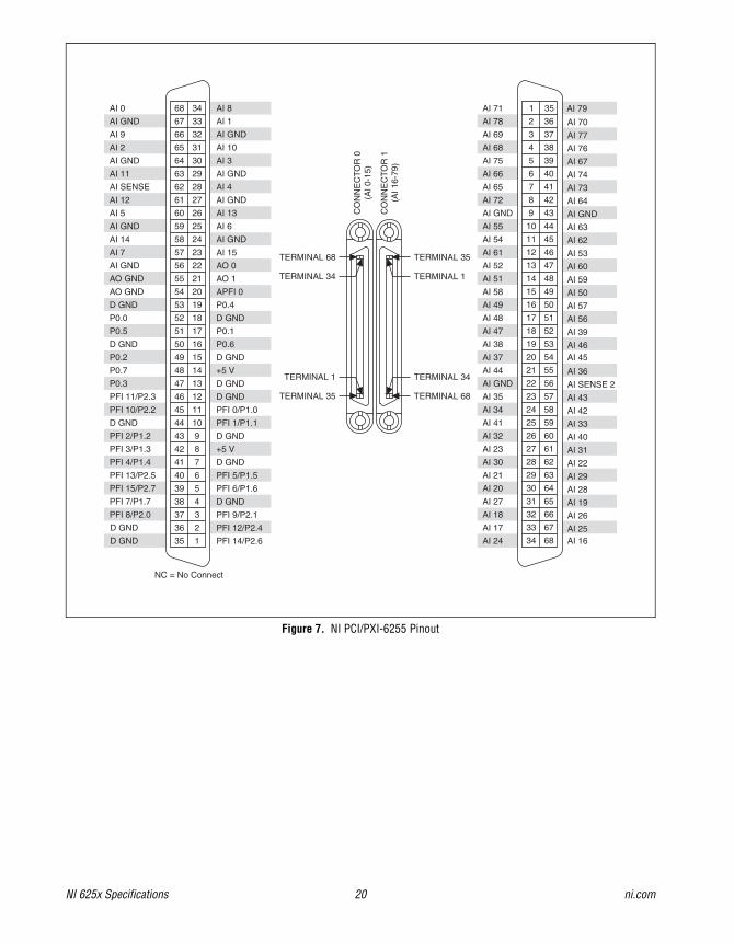
Figure 7. NI PCI/PXI-6255 Pinout
D GND
D GND
PFI 8/P2.0
PFI 7/P1.7
PFI 15/P2.7
PFI 13/P2.5
PFI 4/P1.4
PFI 3/P1.3
PFI 2/P1.2
D GND
PFI 10/P2.2
PFI 11/P2.3
P0.3
P0.7
P0.2
D GND
P0.5
P0.0
D GND
AO GND
AO GND
AI GND
AI 7
AI 14
AI GND
AI 5
AI 12
AI SENSE
AI 11
AI GND
AI 2
AI 9
AI GND
AI 0
PFI 14/P2.6
PFI 9/P2.1
D GND
PFI 5/P1.5
D GND
+5 V
D GND
PFI 12/P2.4
PFI 6/P1.6
PFI 1/P1.1
PFI 0/P1.0
D GND
D GND
+5 V
D GND
P0.6
P0.1
D GND
P0.4
APFI 0
AO 1
AO 0
AI 15
AI GND
AI 6
AI 13
AI GND
AI 4
AI GND
AI 3
AI 10
AI GND
AI 1
AI 868 34
67 33
66 32
65 31
64 30
63 29
62 28
61 27
60 26
59 25
58 24
57 23
56 22
55 21
54 20
53 19
52 18
51 17
50 16
49 15
48 14
47 13
46 12
45 11
44 10
43 9
42 8
41 7
40 6
39 5
38 4
37 3
36 2
35 1 AI 24
AI 17
AI 18
AI 27
AI 20
AI 21
AI 30
AI 23
AI 32
AI 41
AI 34
AI 35
AI GND
AI 44
AI 37
AI 38
AI 47
AI 48
AI 49
AI 58
AI 51
AI 52
AI 61
AI 54
AI 55
AI GND
AI 72
AI 65
AI 66
AI 75
AI 68
AI 69
AI 78
AI 71
AI 16
AI 26
AI 19
AI 29
AI 22
AI 31
AI 40
AI 25
AI 28
AI 33
AI 42
AI 43
AI SENSE 2
AI 36
AI 45AI 46
AI 39
AI 56
AI 57
AI 50
AI 59
AI 60
AI 53
AI 62
AI 63
AI GND
AI 64
AI 73
AI 74
AI 67
AI 76
AI 77
AI 70
AI 791 35
2 36
3 37
4 38
5 39
6 40
7 41
8 42
9 43
10 44
11 45
12 46
13 47
14 48
15 49
16 50
17 51
18 52
19 53
20 54
21 55
22 56
23 57
24 58
25 59
26 60
27 61
28 62
29 63
30 64
31 65
32 66
33 67
34 68
CO
NN
EC
TOR
0(A
I 0-1
5)
CO
NN
EC
TOR
1(A
I 16-
79)
TERMINAL 34
TERMINAL 68
TERMINAL 35
TERMINAL 1
TERMINAL 35
TERMINAL 1
TERMINAL 34
TERMINAL 68
NC = No Connect
© National Instruments Corporation 21 NI 625x Specifications
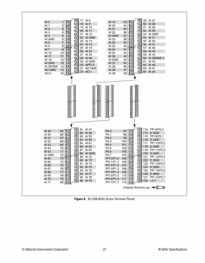
Figure 8. NI USB-6255 Screw Terminal Pinout
17181920212223242526272829303132
AI 8AI 9AI 10AI 11AI 12AI GNDAI 13AI 14AI 15AI 24AI 25AI 26AI GNDAPFI 0AO GNDAO 1
AI 0AI 1AI 2AI 3AI 4AI GNDAI 5AI 6AI 7AI 16AI 17AI 18AI GNDAI SENSEAO GNDAO 0
123456789
10111213141516
49505152535455565758596061626364
AI 27AI 28AI 29AI 30AI GNDAI 31AI 40AI 41AI 42AI 43AI 44AI SENSE 2AI 45AI 46AI 47AI 56
AI 19AI 20AI 21AI 22AI GNDAI 23AI 32AI 33AI 34AI 35AI 36AI GNDAI 37AI 38AI 39AI 48
33343536373839404142434445464748
81828384858687888990919293949596
AI 57AI 58AI 59AI 60AI 61AI 62AI 63AI GNDAI 72AI 73AI 74AI 75AI 76AI 77AI 78AI 79
AI 49AI 50AI 51AI 52AI 53AI 54AI 55AI GNDAI 64AI 65AI 66AI 67AI 68AI 69AI 70AI 71
65666768697071727374757677787980
113114115116117118119120121122123124125126127128
PFI 8/P2.0D GNDPFI 9/P2.1D GNDPFI 10/P2.2D GNDPFI 11/P2.3D GNDPFI 12/P2.4D GNDPFI 13/P2.5D GNDPFI 14/P2.6D GNDPFI 15/P2.7+5 V
P0.0P0.1P0.2P0.3P0.4P0.5P0.6P0.7PFI 0/P1.0PFI 1/P1.1PFI 2/P1.2PFI 3/P1.3PFI 4/P1.4PFI 5/P1.5PFI 6/P1.6PFI 7/P1.7
979899
100101102103104105106107108109110111112
Chassis Ground Lug
NI 625x Specifications 22 ni.com
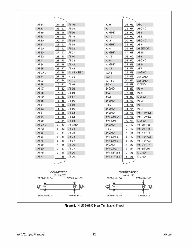
Figure 9. NI USB-6255 Mass Termination Pinout
AI 71
AI 78
AI 69
AI 68
AI 75
AI 66
AI 65
AI 72
AI GND
AI 55
AI 54
AI 61
AI 52
AI 51
AI 58
AI 49
AI 48
AI 47
AI 38AI 37
AI 44
AI GND
AI 35
AI 34
AI 41
AI 32
AI 23
AI 30
AI 21
AI 20
AI 27
AI 18
AI 17
AI 24
AI 79
AI 77
AI 76
AI 74
AI 73
AI 64
AI GND
AI 70
AI 67
AI 63
AI 62
AI 53
AI 60
AI 59
AI 50
AI 57
AI 56
AI 39
AI 46AI 45
AI 36
AI SENSE 2
AI 43
AI 42
AI 33
AI 40
AI 31
AI 22
AI 29
AI 28
AI 19
AI 26
AI 25
AI 16
1
2
3
4
5
6
7
8
9
10
11
12
13
14
15
16
17
18
19
20
21
22
23
24
25
26
27
28
29
30
31
32
33
34
35
36
37
38
39
40
41
42
43
44
45
46
47
48
49
50
51
52
53
54
55
56
57
58
59
60
61
62
63
64
65
66
67
68
CONNECTOR 1(AI 16–79)
PFI 14/P2.6
PFI 12/P2.4
PFI 9/P2.1
D GND
PFI 6/P1.6
PFI 5/P1.5
D GND
+5 V
D GND
PFI 1/P1.1
PFI 0/P1.0
D GND
D GND
+5 V
D GND
P0.6
P0.1
D GND
P0.4APFI 0
AO 1
AO 0
AI 15
AI GND
AI 6
AI 13
AI GND
AI 4
AI GND
AI 3
AI 10
AI GND
AI 1
AI 8
D GND
PFI 8/P2.0
PFI 7/P1.7
PFI 13/P2.5
PFI 4/P1.4
PFI 3/P1.3
PFI 2/P1.2
D GND
PFI 15/P2.7
D GND
PFI 10/P2.2
PFI 11/P2.3
P0.3
P0.7
P0.2
D GND
P0.5
P0.0
D GNDAO GND
AO GND
AI GND
AI 7
AI 14
AI GND
AI 5
AI 12
AI SENSE
AI 11
AI GND
AI 2
AI 9
AI GND
AI 0
1
2
3
4
5
6
7
8
9
10
11
12
13
14
15
16
17
18
19
20
21
22
23
24
25
26
27
28
29
30
31
32
33
34
35
36
37
38
39
40
41
42
43
44
45
46
47
48
49
50
51
52
53
54
55
56
57
58
59
60
61
62
63
64
65
66
67
68
CONNECTOR 0(AI 0–15)
TERMINAL 34
TERMINAL 68
TERMINAL 1
TERMINAL 35
TERMINAL 34
TERMINAL 68
TERMINAL 1
TERMINAL 35
© National Instruments Corporation 23 NI 625x Specifications
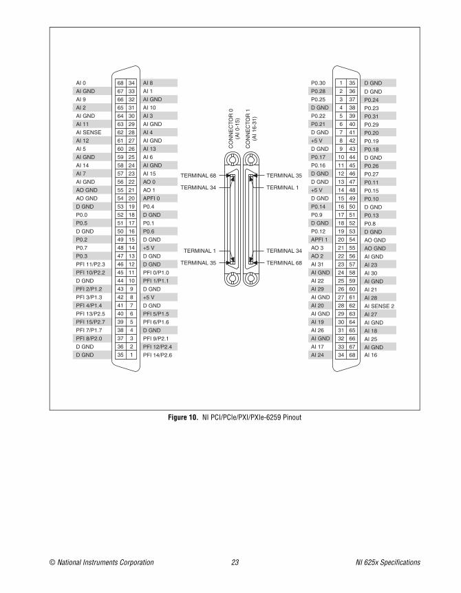
Figure 10. NI PCI/PCIe/PXI/PXIe-6259 Pinout
CO
NN
EC
TOR
0(A
I 0-1
5)
CO
NN
EC
TOR
1(A
I 16-
31)
D GND
D GND
PFI 8/P2.0
PFI 7/P1.7
PFI 15/P2.7
PFI 13/P2.5
PFI 4/P1.4
PFI 3/P1.3
PFI 2/P1.2
D GND
PFI 10/P2.2
PFI 11/P2.3
P0.3
P0.7
P0.2
D GND
P0.5
P0.0
D GND
AO GND
AO GND
AI GND
AI 7
AI 14
AI GND
AI 5
AI 12
AI SENSE
AI 11
AI GND
AI 2
AI 9
AI GND
AI 0
PFI 14/P2.6
PFI 9/P2.1
D GND
PFI 5/P1.5
D GND
+5 V
D GND
PFI 12/P2.4
PFI 6/P1.6
PFI 1/P1.1
PFI 0/P1.0
D GND
D GND
+5 V
D GND
P0.6
P0.1
D GND
P0.4
APFI 0
AO 1
AO 0
AI 15
AI GND
AI 6
AI 13
AI GND
AI 4
AI GND
AI 3
AI 10
AI GND
AI 1
AI 868 34
67 33
66 32
65 31
64 30
63 29
62 28
61 27
60 26
59 25
58 24
57 23
56 22
55 21
54 20
53 19
52 18
51 17
50 16
49 15
48 14
47 13
46 12
45 11
44 10
43 9
42 8
41 7
40 6
39 5
38 4
37 3
36 2
35 1 AI 24
AI 17
AI GND
AI 26
AI 19
AI GND
AI 20
AI GND
AI 29
AI 22
AI GND
AI 31
AO 2
AO 3
APFI 1
P0.12
D GND
P0.9
P0.14
D GND
+5 V
D GND
D GND
P0.16
P0.17
D GND
+5 V
D GND
P0.21
P0.22
D GND
P0.25
P0.28
P0.30
AI 16
AI 25
AI 18
AI 27
AI SENSE 2
AI 28
AI 21
AI GND
AI GND
AI GND
AI 30
AI 23
AI GND
AO GND
AO GND
D GND
P0.8
P0.13
D GND
P0.10
P0.15
P0.11
P0.27
P0.26
D GND
P0.18
P0.19
P0.20
P0.29
P0.31
P0.23
P0.24
D GND
D GND1 35
2 36
3 37
4 38
5 39
6 40
7 41
8 42
9 43
10 44
11 45
12 46
13 47
14 48
15 49
16 50
17 51
18 52
19 53
20 54
21 55
22 56
23 57
24 58
25 59
26 60
27 61
28 62
29 63
30 64
31 65
32 66
33 67
34 68
TERMINAL 34
TERMINAL 68
TERMINAL 35
TERMINAL 1
TERMINAL 35
TERMINAL 1
TERMINAL 34
TERMINAL 68
NI 625x Specifications 24 ni.com
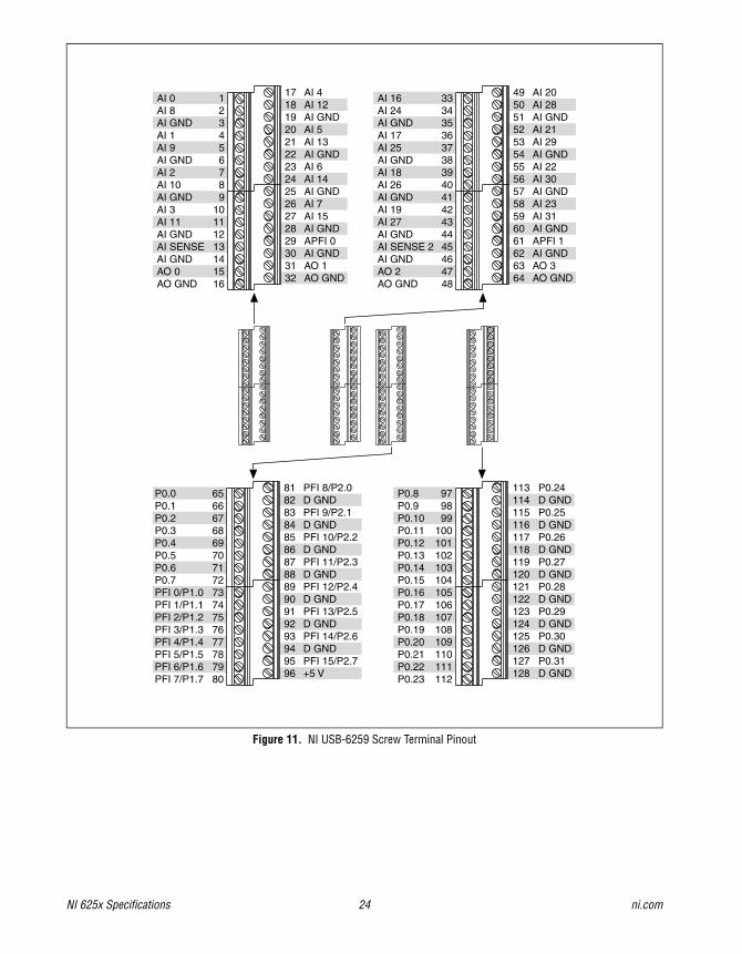
Figure 11. NI USB-6259 Screw Terminal Pinout
17181920212223242526272829303132
AI 4AI 12AI GNDAI 5AI 13AI GNDAI 6AI 14AI GNDAI 7AI 15AI GNDAPFI 0AI GNDAO 1AO GND
AI 0AI 8AI GNDAI 1AI 9AI GNDAI 2AI 10AI GNDAI 3AI 11AI GNDAI SENSEAI GNDAO 0AO GND
123456789
10111213141516
49505152535455565758596061626364
AI 20AI 28AI GNDAI 21AI 29AI GNDAI 22AI 30AI GNDAI 23AI 31AI GNDAPFI 1AI GNDAO 3AO GND
AI 16AI 24AI GNDAI 17AI 25AI GNDAI 18AI 26AI GNDAI 19AI 27AI GNDAI SENSE 2AI GNDAO 2AO GND
33343536373839404142434445464748
81828384858687888990919293949596
PFI 8/P2.0D GNDPFI 9/P2.1D GNDPFI 10/P2.2D GNDPFI 11/P2.3D GNDPFI 12/P2.4D GNDPFI 13/P2.5D GNDPFI 14/P2.6D GNDPFI 15/P2.7+5 V
P0.0P0.1P0.2P0.3P0.4P0.5P0.6P0.7PFI 0/P1.0PFI 1/P1.1PFI 2/P1.2PFI 3/P1.3PFI 4/P1.4PFI 5/P1.5PFI 6/P1.6PFI 7/P1.7
65666768697071727374757677787980
113114115116117118119120121122123124125126127128
P0.24D GNDP0.25D GNDP0.26D GNDP0.27D GNDP0.28D GNDP0.29D GNDP0.30D GNDP0.31D GND
P0.8P0.9P0.10P0.11P0.12P0.13P0.14P0.15P0.16P0.17P0.18P0.19P0.20P0.21P0.22P0.23
979899
100101102103104105106107108109110111112
© National Instruments Corporation 25 NI 625x Specifications
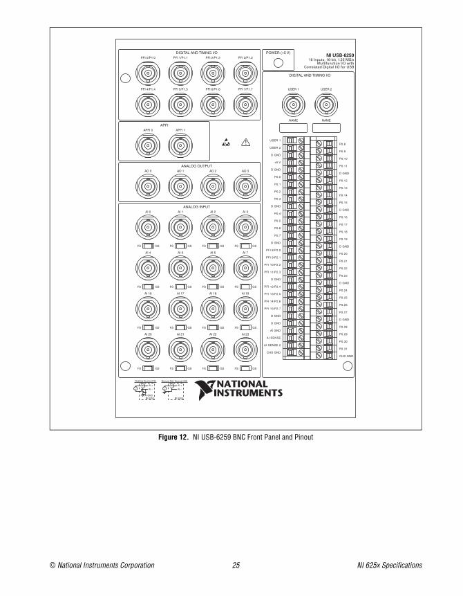
Figure 12. NI USB-6259 BNC Front Panel and Pinout
National Instruments, NI, ni.com, and LabVIEW are trademarks of National Instruments Corporation. Refer to the Terms of Use section on ni.com/legal for more information about National Instruments trademarks. Other product and company names mentioned herein are trademarks or trade names of their respective companies. For patents covering National Instruments products, refer to the appropriate location: Help»Patents in your software, the patents.txt file on your CD, or ni.com/patents.
© 2004–2007 National Instruments Corporation. All rights reserved. 371291H-01 Jun07
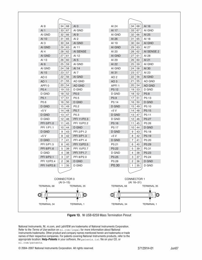
Figure 13. NI USB-6259 Mass Termination Pinout
PFI 14/P2.6
PFI 12/P2.4
PFI 9/P2.1
D GND
PFI 6/P1.6
PFI 5/P1.5
D GND
+5 V
D GND
PFI 1/P1.1
PFI 0/P1.0
D GND
D GND
+5 V
D GND
P0.6
P0.1
D GND
P0.4APFI 0
AO 1
AO 0
AI 15
AI GND
AI 6
AI 13
AI GND
AI 4
AI GND
AI 3
AI 10
AI GND
AI 1
AI 8
D GND
PFI 8/P2.0
PFI 7/P1.7
PFI 13/P2.5
PFI 4/P1.4
PFI 3/P1.3
PFI 2/P1.2
D GND
PFI 15/P2.7
D GND
PFI 10/P2.2
PFI 11/P2.3
P0.3
P0.7
P0.2
D GND
P0.5
P0.0
D GNDAO GND
AO GND
AI GND
AI 7
AI 14
AI GND
AI 5
AI 12
AI SENSE
AI 11
AI GND
AI 2
AI 9
AI GND
AI 0
1
2
3
4
5
6
7
8
9
10
11
12
13
14
15
16
17
18
19
20
21
22
23
24
25
26
27
28
29
30
31
32
33
34
35
36
37
38
39
40
41
42
43
44
45
46
47
48
49
50
51
52
53
54
55
56
57
58
59
60
61
62
63
64
65
66
67
68
P0.30P0.28
P0.25
D GND
P0.22
P0.21
D GND
+5 V
D GND
P0.17
P0.16
D GND
D GND
+5 V
D GND
P0.14
P0.9
D GND
P0.12APFI 1
AO 3
AO 2
AI 31
AI GND
AI 22
AI 29
AI GND
AI 20
AI GND
AI 19
AI 26
AI GND
AI 17
AI 24
D GND
P0.24
P0.23
P0.29
P0.20
P0.19
P0.18
D GND
P0.31
D GND
P0.26
P0.27
P0.11
P0.15
P0.10
D GND
P0.13
P0.8
D GNDAO GND
AO GND
AI GND
AI 23
AI 30
AI GND
AI 21
AI 28
AI SENSE 2
AI 27
AI GND
AI 18
AI 25
AI GND
AI 16
1
2
3
4
5
6
7
8
9
10
11
12
13
14
15
16
17
18
19
20
21
22
23
24
25
26
27
28
29
30
31
32
33
34
35
36
37
38
39
40
41
42
43
44
45
46
47
48
49
50
51
52
53
54
55
56
57
58
59
60
61
62
63
64
65
66
67
68
CONNECTOR 0(AI 0–15)
CONNECTOR 1(AI 16–31)
TERMINAL 34
TERMINAL 68
TERMINAL 1
TERMINAL 35
TERMINAL 34
TERMINAL 68
TERMINAL 1
TERMINAL 35