Embed Size (px)
Citation preview
FEATURES 10-BIT RESOLUTION
RAIL-TO-RAIL OUTPUT
ONBOARD NONVOLATILE MEMORY
IOUT: 100mA
LOW SUPPLY CURRENT: 900 µA
SUPPLY VOLTAGE: 7V to 18V
DIGITAL SUPPLY: 2.0V to 5.5V
INDUSTRY-STANDARD, TWO-WIREINTERFACE
HIGH ESD RATING:2kV HBM, 500V CDM
APPLICATIONS LCD PANEL V COM CALIBRATION
LCD PANEL BRIGHTNESS AND CONTRASTCONTROL
POTENTIOMETER REPLACEMENT
MOTOR DRIVE
PROGRAMMABLE POWER SUPPLY
PROGRAMMABLE OFFSET ADJUSTMENT
ACTUATOR CONTROL
BUF01900, BUF01901 RELATED PRODUCTSFEATURES PRODUCT
22V High Supply Voltage Gamma Buffers BUF11705
12--Channel Programmable Buffer, 10-Bit, VCOM BUF12800
20-Channel Programmable Buffer, 10-Bit, VCOM BUF20800
16-Channel Programmable Buffer with Memory BUF16820
20-Channel Programmable Buffer with Memory BUF20820
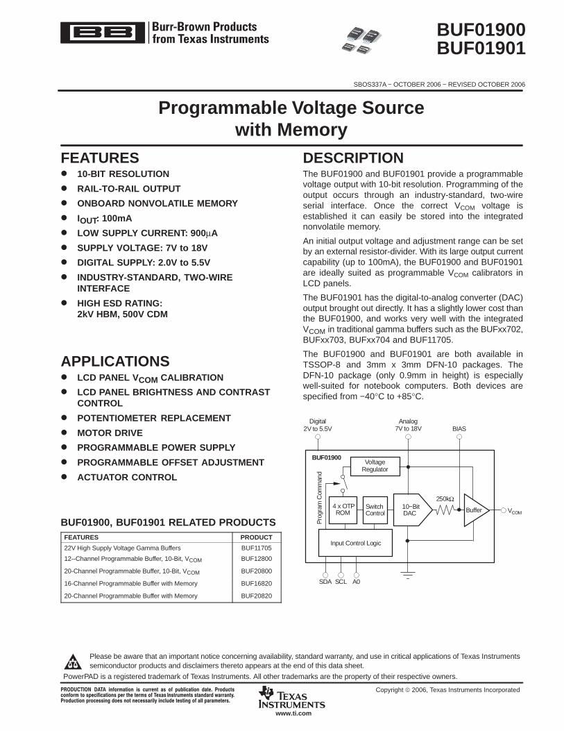
DESCRIPTIONThe BUF01900 and BUF01901 provide a programmablevoltage output with 10-bit resolution. Programming of theoutput occurs through an industry-standard, two-wireserial interface. Once the correct VCOM voltage isestablished it can easily be stored into the integratednonvolatile memory.
An initial output voltage and adjustment range can be setby an external resistor-divider. With its large output currentcapability (up to 100mA), the BUF01900 and BUF01901are ideally suited as programmable VCOM calibrators inLCD panels.
The BUF01901 has the digital-to-analog converter (DAC)output brought out directly. It has a slightly lower cost thanthe BUF01900, and works very well with the integratedVCOM in traditional gamma buffers such as the BUFxx702,BUFxx703, BUFxx704 and BUF11705.
The BUF01900 and BUF01901 are both available inTSSOP-8 and 3mm x 3mm DFN-10 packages. TheDFN-10 package (only 0.9mm in height) is especiallywell-suited for notebook computers. Both devices arespecified from −40°C to +85°C.
Analog7V to 18V
Digital2V to 5.5V BIAS
SDA
Input Control Logic
SCL A0
10−BitDAC
4 x OTPROM
SwitchControl
VoltageRegulator
Pro
gram
Com
man
d
BUF01900
250kΩ
Buffer VCOM
BUF01900BUF01901
SBOS337A − OCTOBER 2006 − REVISED OCTOBER 2006
Programmable Voltage Sourcewith Memory
! !
www.ti.com
Copyright 2006, Texas Instruments Incorporated
Please be aware that an important notice concerning availability, standard warranty, and use in critical applications of Texas Instrumentssemiconductor products and disclaimers thereto appears at the end of this data sheet.
PowerPAD is a registered trademark of Texas Instruments. All other trademarks are the property of their respective owners.

"#$%&$$"#$%&$%
SBOS337A − OCTOBER 2006 − REVISED OCTOBER 2006
www.ti.com
2
This integrated circuit can be damaged by ESD. Texas Instruments recommends that all integrated circuits be handled with appropriateprecautions. Failure to observe proper handling and installation procedures can cause damage.
ESD damage can range from subtle performance degradation to complete device failure. Precision integrated circuits may be moresusceptible to damage because very small parametric changes could cause the device not to meet its published specifications.
ABSOLUTE MAXIMUM RATINGS (1)
Supply Voltage, VS +20V. . . . . . . . . . . . . . . . . . . . . . . . . . . . . . . . . . . . . . . . . . . . . . . . . . . . . . . . . . . . . . . . . . . . . . . . . . . . . . . . . . . . . . . . . . . . . . . . . . Supply Voltage, VSD +6V. . . . . . . . . . . . . . . . . . . . . . . . . . . . . . . . . . . . . . . . . . . . . . . . . . . . . . . . . . . . . . . . . . . . . . . . . . . . . . . . . . . . . . . . . . . . . . . . . . Signal Input Terminals,
BIAS:Voltage −0.5V to VS +0.5V. . . . . . . . . . . . . . . . . . . . . . . . . . . . . . . . . . . . . . . . . . . . . . . . . . . . . . . . . . . . . . . . . . . . . . . . . . . . . . . . . . . . . . . . . . . . . . .
SCL, SDA, A0, A1:Voltage −0.5V to +6V. . . . . . . . . . . . . . . . . . . . . . . . . . . . . . . . . . . . . . . . . . . . . . . . . . . . . . . . . . . . . . . . . . . . . . . . . . . . . . . . . . . . . . . . . . . . . . . . . . . Current ±10mA. . . . . . . . . . . . . . . . . . . . . . . . . . . . . . . . . . . . . . . . . . . . . . . . . . . . . . . . . . . . . . . . . . . . . . . . . . . . . . . . . . . . . . . . . . . . . . . . . . . . . . . .
Output Short Circuit(2) Continuous. . . . . . . . . . . . . . . . . . . . . . . . . . . . . . . . . . . . . . . . . . . . . . . . . . . . . . . . . . . . . . . . . . . . . . . . . . . . . . . . . . . . . . . . . . . Operating Temperature −40°C to +95°C. . . . . . . . . . . . . . . . . . . . . . . . . . . . . . . . . . . . . . . . . . . . . . . . . . . . . . . . . . . . . . . . . . . . . . . . . . . . . . . . . . . . . . Storage Temperature −65°C to +150°C. . . . . . . . . . . . . . . . . . . . . . . . . . . . . . . . . . . . . . . . . . . . . . . . . . . . . . . . . . . . . . . . . . . . . . . . . . . . . . . . . . . . . . . Junction Temperature +125°C. . . . . . . . . . . . . . . . . . . . . . . . . . . . . . . . . . . . . . . . . . . . . . . . . . . . . . . . . . . . . . . . . . . . . . . . . . . . . . . . . . . . . . . . . . . . . . . ESD Rating:
Human Body Model (HBM) 2000V. . . . . . . . . . . . . . . . . . . . . . . . . . . . . . . . . . . . . . . . . . . . . . . . . . . . . . . . . . . . . . . . . . . . . . . . . . . . . . . . . . . . . . . . Charged-Device Model (CDM) 500V. . . . . . . . . . . . . . . . . . . . . . . . . . . . . . . . . . . . . . . . . . . . . . . . . . . . . . . . . . . . . . . . . . . . . . . . . . . . . . . . . . . . . .
(1) Stresses above these ratings may cause permanent damage. Exposure to absolute maximum conditions for extended periods may degradedevice reliability. These are stress ratings only, and functional operation of the device at these or any other conditions beyond those specified isnot supported.
(2) Short-circuit to ground.
ORDERING INFORMATION(1)
PRODUCT PACKAGE-LEAD PACKAGE DESIGNATOR PACKAGE MARKING
BUF01900 DFN-10 DRC BOO
BUF01900 TSSOP-8 PW F01900
BUF01901 DFN-10 DRC BOP
BUF01901 TSSOP-8 PW F01901(1) For the most current package and ordering information, see the Package Option Addendum at the end of this document, or see the TI web site
at www.ti.com.
PIN CONFIGURATIONS
NC = No connection
VS
VCOM
BIAS
GND
DGND
SDA
SCL
A0
A1
VSD
1
2
3
4
5
10
9
8
7
6
ExposedThermalDie Pad
onUnderside
DFN−10
BUF01900
VS
NC
BIAS
GND
DGND
SDA
SCL
A0
A1
VSD
1
2
3
4
5
10
9
8
7
6
ExposedThermalDie Pad
onUnderside
DFN−10
BUF01901
VS
VCOM
BIAS
GND
SDA
SCL
A0
VSD
1
2
3
4
8
7
6
5
BUF01900
TSSOP−8
VS
NC
BIAS
GND
SDA
SCL
A0
VSD
1
2
3
4
8
7
6
5
BUF01901
TSSOP−8

"#$%&$$"#$%&$%
SBOS337A − OCTOBER 2006 − REVISED OCTOBER 2006
www.ti.com
3
ELECTRICAL CHARACTERISTICS Boldface limits apply over the specified temperature range, TA = −40°C to +85°C.At TA = +25°C, VS = 18V, VSD = 5V, RL = 1.5kΩ connected to ground, and CL = 200pF, unless otherwise noted.
BUF01900, BUF01901
PARAMETER CONDITIONS MIN TYP MAX UNIT
ANALOGVCOM Output Swing (1) Sourcing 10mA, Code 1023 17.7 17.8 V
Sinking 10mA, Code 00 0.6 1 VSourcing 100mA, Code 1023 15 16 V
Sinking 100mA, Code 00 0.75 1 VVCOM Output Reset and Power-Up Value(1) OTP not programmed, Code 512 VS/2 VNominal VBIAS Output Impedance No Load on VBIAS, VCOM 250 kΩProgram to Out Delay tD 5 µsOutput Accuracy 1V < VCOM < 17.7 20 50 mVLoad Regulation REG VOUT = VS/2, IOUT = +50mA to −50mA Step 0.5 1.5 mV/mAVCOM(1)
Offset ±5 ±25 mVOffset Drift −25°C to +100°C 5 µV/°CCommon-Mode Range 0.8 to 18 VCommon-Mode Rejection CMR 0.8V < VIN < 17.9V 85 dBSlew Rate 5 V/µs
VBIAS No Load on VBIASIntegral Nonlinearity INL 0.1 2 LSBDifferential Nonlinearity DNL 0.1 2 LSBGain Error 0.1 1 %FSCAccuracy 20 50 mV
ANALOG POWER SUPPLYOperating Range(2) VS 7 18 VTotal Analog Supply Current IS Output at Reset Values, No Load 0.9 1.5 mA
over Temperature 1.5 mA
DIGITALLogic 1 Input Voltage VIH 0.7 × VSD VLogic 0 Input Voltage VIL 0.3 × VSD VLogic 0 Output Voltage VOL ISINK = 3mA 0.15 0.4 VInput Leakage ±0.01 ±10 µAClock Frequency fCLK Standard/Fast Mode 400 kHz
High-Speed Mode 3.4 MHz
DIGITAL POWER SUPPLYOperating Voltage Range VSD 2.0 5.5 VDigital Supply Current(2) ISD 25 50 µA
over Temperature 100 µA
TEMPERATURESpecified Temperature Range −40 +85 °COperating Temperature Range Junction Temperature < 125°C −40 +95 °CStorage Temperature Range −65 +150 °CThermal Resistance JA
TSSOP-8 150 °C/WDFN-10 47 °C/W
(1) BUF01900 only.(2) Minimum analog supply voltage is 8.5V when programming OTP memory.

"#$%&$$"#$%&$%
SBOS337A − OCTOBER 2006 − REVISED OCTOBER 2006
www.ti.com
4
TYPICAL CHARACTERISTICSAt TA = +25°C, VS = 18V, VSD = 5V, RL = 1.5kΩ connected to ground, and CL = 200pF, unless otherwise noted.
Figure 1
1.5
1.0
0.5
0
Ana
log
Sup
ply
Cur
rent
(mA
)
ANALOG SUPPLY CURRENT vs TEMPERATURE
−40 −20 0 10040 60 8020
Temperature (C)
VSD = 8V
VS = 18V
Figure 2
50
40
30
20
10
0
Dig
italS
uppl
yC
urre
nt(µ
A)
DIGITAL SUPPLY CURRENT vs TEMPERATURE
−40 −20 0 10040 60 8020
Temperature (C)
VSD = 5V
VSD = 2V
Figure 3
25
20
15
10
5
0
−5
−10
−15
−20
−25
VO
S(m
V)
BUFFER OFFSET VOLTAGE vs TEMPERATURE(VS = 18V, VSD = 5V)
−40 −20 0 10040 60 8020
Temperature (C)
PDS limits are ±25mV
Figure 4
20
18
16
14
12
10
8
6
4
2
0
VO
UT
(V)
OUTPUT VOLTAGE vs OUTPUT CURRENT
0 25 10050 75
IOUT (mA)
Sourcing, Code = 3FFh
VS = 18V
Sinking, Code = 000h
Figure 5
1.5
1.0
0.5
0
−0.5
−1.0
−1.5
INL
Err
or(L
SB
)
INTEGRAL NONLINEARITY ERROR vs INPUT CODE
0 128 256 384 512 1024
Input Code
640 768 896
10 Typical Units Shown
Figure 6
DN
LE
rro
r(L
SB
)
DIFFERENTIAL NONLINEARITY ERRORvs INPUT CODE
1.5
1.0
0.5
0
−0.5
−1.0
−1.50 128 256 384 512 1024
Input Decimal Code
640 768 896
10 Typical Units Shown

"#$%&$$"#$%&$%
SBOS337A − OCTOBER 2006 − REVISED OCTOBER 2006
www.ti.com
5
TYPICAL CHARACTERISTICS (cont)At TA = +25°C, VS = 18V, VSD = 5V, RL = 1.5kΩ connected to ground, and CL = 200pF, unless otherwise noted.
Figure 7
5V/d
iv
VCOM BUFFER SLEW RATE
Time (1µs/div)
1 2
(1) VBIAS
(2) VCOM
Figure 8
5V/d
iv
BUFFER LARGE SIGNAL STEP RESPONSE
Time (1µs/div)
1 2
(1) VBIAS
(2) VCOM
Figure 9
100
mA
/div
500
mV
/div
LOAD REGULATION vs CAPACITANCE
Time (1µs/div)
1
C = 0.1µF
C = 10µF
C = 1µF
2.7nF
C
1
Figure 10
100m
A/d
iv5
00m
V/d
iv
LOAD REGULATION vs CAPACITANCE
Time (1µs/div)
1
2
C = 1µF
C = 10µF
C = 0.1µF C = 10µF
C = 1µF
10 Ω1
2 .7 nF
C
2
Figure 11
20m
V/d
iv10
0mA
/div
LOAD REGULATION WITH 100µF CAPACITOR
Time (1µs/div)
1
2.7nF
100µ F
1
Figure 12
50m
V/d
iv1
00m
A/d
iv
LOAD REGULATION WITH 10µF CAPACITOR
Time (1µs/div)
1
2.7nF
10 µF
1
"#$%&$$"#$%&$%
SBOS337A − OCTOBER 2006 − REVISED OCTOBER 2006
www.ti.com
6
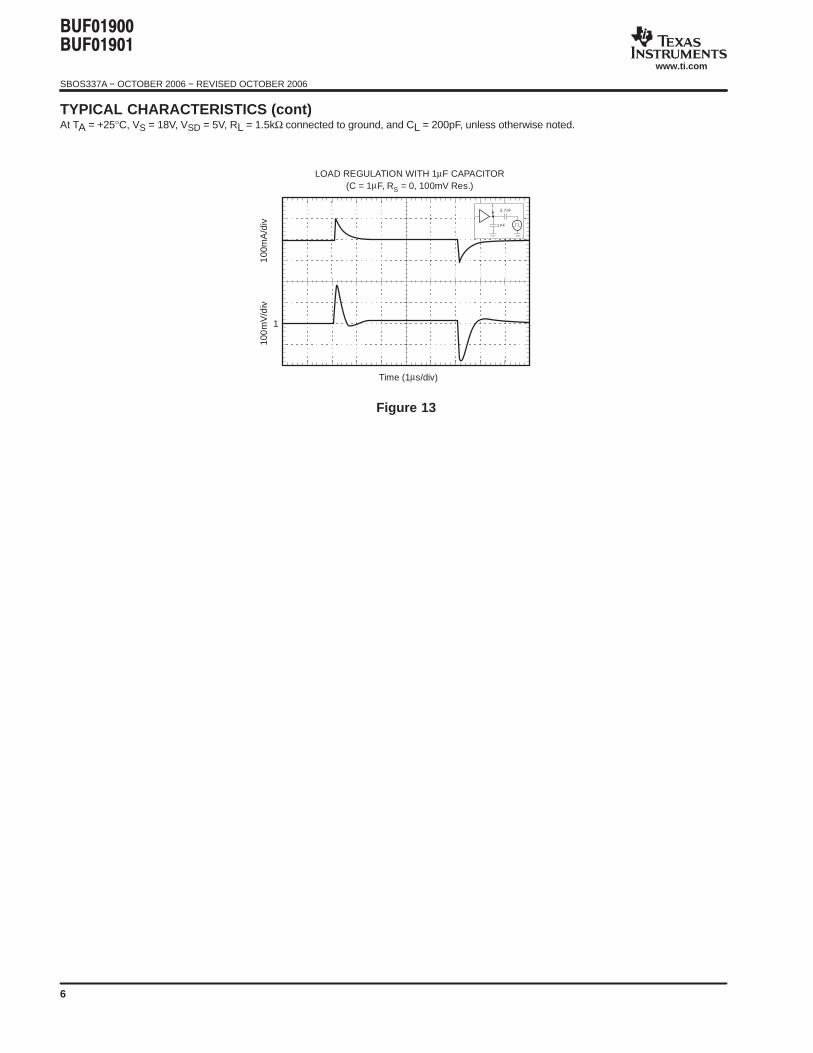
TYPICAL CHARACTERISTICS (cont)At TA = +25°C, VS = 18V, VSD = 5V, RL = 1.5kΩ connected to ground, and CL = 200pF, unless otherwise noted.
Figure 13
100
mV
/div
100
mA
/div
LOAD REGULATION WITH 1µF CAPACITOR(C = 1µF, RS = 0, 100mV Res.)
Time (1µs/div)
1
2.7nF
1 µ F
1

"#$%&$$"#$%&$%
SBOS337A − OCTOBER 2006 − REVISED OCTOBER 2006
www.ti.com
7
APPLICATIONS INFORMATIONOVERVIEWThe BUF0190x family of products consists of a 10-bit digi-tal-to-analog converter (DAC) that is programmed throughan industry-standard two-wire interface. It contains on-chip nonvolatile memory that stores a specific DAC valuethat is read at power-up. The BUF0190x family consists oftwo devices: The BUF01900 contains a voltage buffer thatis capable of driving high-current; the BUF01901 is a low-er-cost version without the buffer. The BUF0190x is espe-cially well-suited for VCOM calibration in LCD panels; how-ever, it can also be used in many other applications.Figure 14 shows the BUF01900 in a typical configuration.
BUF01900: ON-CHIP BUFFER
Unlike many programmable VCOM calibrators on the mar-ket, the BUF01900 offers an integrated VCOM buffer withhigh current output drive capability. The output is capableof delivering peak currents over 100mA to within 4V fromthe positive supply and to within 2V from the negative sup-ply. Using this option is very cost-effective and convenientin systems that do not use multi-channel gamma bufferswith integrated VCOM drive. Figure 15 shows theBUF01900 in a typical configuration.
(1)
TimingController
0.1µF
0.1µF
VS
VSD
VCOM
(2)
(2)VS
10µF
10kΩ 10kΩ
+ 1
2
3
4
8
7
6
5
SDA
SCL
A0
VSD
VS
VCOM
VBIAS
GND
(1) Optional −may be needed for stability.(2) Optional −see application text for component selection.
BUF01900
NOTES:
Figure 14. Typical Application Diagram
BIAS
250kΩ
Analog7V to 18V
R1 R2
Digital2V to 5.5V
SDA
Input Control Logic
SCL A0
10−BitDAC
4 x OTPROM
SwitchControl
VoltageRegulator
Pro
gram
Com
man
d
BUF01900
VCOMBuffer
VCOMPanel
Figure 15. BUF01900 Typical Configuration
"#$%&$$"#$%&$%
SBOS337A − OCTOBER 2006 − REVISED OCTOBER 2006
www.ti.com
8
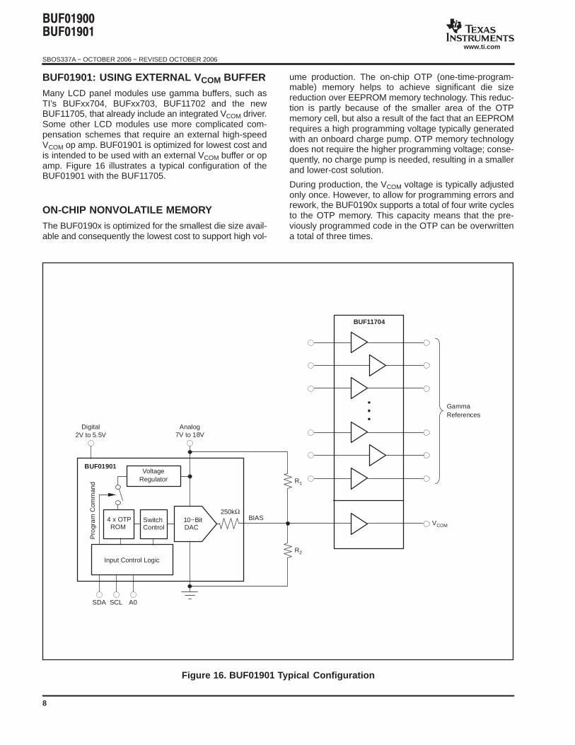
BUF01901: USING EXTERNAL V COM BUFFERMany LCD panel modules use gamma buffers, such asTI’s BUFxx704, BUFxx703, BUF11702 and the newBUF11705, that already include an integrated VCOM driver.Some other LCD modules use more complicated com-pensation schemes that require an external high-speedVCOM op amp. BUF01901 is optimized for lowest cost andis intended to be used with an external VCOM buffer or opamp. Figure 16 illustrates a typical configuration of theBUF01901 with the BUF11705.
ON-CHIP NONVOLATILE MEMORYThe BUF0190x is optimized for the smallest die size avail-able and consequently the lowest cost to support high vol-
ume production. The on-chip OTP (one-time-program-mable) memory helps to achieve significant die sizereduction over EEPROM memory technology. This reduc-tion is partly because of the smaller area of the OTPmemory cell, but also a result of the fact that an EEPROMrequires a high programming voltage typically generatedwith an onboard charge pump. OTP memory technologydoes not require the higher programming voltage; conse-quently, no charge pump is needed, resulting in a smallerand lower-cost solution.
During production, the VCOM voltage is typically adjustedonly once. However, to allow for programming errors andrework, the BUF0190x supports a total of four write cyclesto the OTP memory. This capacity means that the pre-viously programmed code in the OTP can be overwrittena total of three times.
250kΩBIAS
R1
VoltageRegulator
Analog7V to 18V
Digital2V to 5.5V
SDA
Input Control Logic
SCL A0
10−BitDAC
4 x OTPROM
SwitchControl
Pro
gra
mC
omm
and
BUF01901
GammaReferences
BUF11704
VCOM
R2
Figure 16. BUF01901 Typical Configuration

"#$%&$$"#$%&$%
SBOS337A − OCTOBER 2006 − REVISED OCTOBER 2006
www.ti.com
9
POWER-SUPPLY VOLTAGEThe BUF0190x can be powered using an analog supplyvoltage from 7V to 18V, and a digital supply from 2V to5.5V. The digital supply must be applied prior to the analogsupply to avoid excessive current and power consumption.
During programming of the OTP, the analog power supplymust be at least 8.5V.
BUFFER INPUT AND OUTPUT RANGEThe integrated buffer has a single p-channel input stage.The input range includes the positive supply and extendsdown to typically 0.8V above the negative supply (GND).In a typical LCD application, this is normally sufficient be-cause the nominal VCOM level is often close to V2/2 and,therefore, fairly far away from either supply rail. In addition,the adjustment range is usually not much larger than 1V ineither direction of the nominal VCOM voltage. In applica-tions requiring a wider output swing, the output voltage tothe buffer should be limited to approximately 0.8V abovethe negative power supply to keep the buffer input stagein its linear operating region. For lower input voltages, theoutput results might not be valid; however, they will alsonot lead to damage of the device.The Rail-to-Rail output stage is designed to drive largepeak currents greater than 100mA.
TWO-WIRE BUS OVERVIEWThe BUF0190x communicates through an industry-stan-dard, two-wire interface to receive data in slave mode. Thisstandard uses a two-wire, open-drain interface that sup-ports multiple devices on a single bus. Bus lines are drivento a logic low level only. The device that initiates the com-munication is called a master, and the devices controlledby the master are slaves. The master generates the serialclock on the clock signal line (SCL), controls the bus ac-cess, and generates START and STOP conditions.To address a specific device, the master initiates a STARTcondition by pulling the data signal line (SDA) from a HIGHto LOW logic level while SCL is HIGH. All slaves on the busshift in the slave address byte, with the last bit indicatingwhether a read or write operation is intended. During theninth clock pulse, the slave being addressed responds tothe master by generating an Acknowledge and pullingSDA LOW.Data transfer is then initiated and eight bits of data aresent, followed by an Acknowledge bit. During data trans-fer, SDA must remain stable while SCL is HIGH. Anychange in SDA while SCL is HIGH will be interpreted as aSTART or STOP condition.Once all data has been transferred, the master generatesa STOP condition, indicated by pulling SDA from LOW toHIGH while SCL is HIGH.
The BUF0190x can act only as a slave device; therefore,it never drives SCL. The SCL is only an input for theBUF0190x.
ADDRESSING THE BUF01900 ANDBUF01901The address of the BUF0190x in the TSSOP-8 packageis 111011x, where x is the state of the A0 pin. When theA0 pin is LOW, the device acknowledges on address 76h.If the A0 pin is HIGH, the device acknowledges on address77h. Table 1 summarizes device addresses.
Table 1. Quick-Reference Table of AddressesDEVICE/COMPONENT ADDRESS
TSSOP Package:
A0 pin is LOW(device will acknowledge on address 76h)
1110110
A0 pin is HIGH(device will acknowledge on address 77h)
1110111
DFN Package:
A0 pin is LOW, A1 is LOW(device will acknowledge on address 74h)
1110100
A0 pin is HIGH, A1 is LOW(device will acknowledge on address 75h)
1110101
A0 pin is LOW, A1 is HIGH(device will acknowledge on address 76h)
1110110
A0 pin is HIGH, A1 is HIGH(device will acknowledge on address 77h)
1110111
The address of the BUF0190x in the DFN-10 package is11101yx, where x is the state of the A0 pin and y is the stateof the A1 pin. When the A0 and A1 pins are both LOW, thedevice acknowledges on address 74h. If the A0 is HIGHand A1 is LOW, the device acknowledges on address 75h.When the A0 is LOW, and A1 is HIGH, the device acknowl-edges on address 76h. If the A0 and A1 pins are bothHIGH, the device address is 77h.
Other addresses are possible through a simple maskchange. Contact your TI representative for ordering infor-mation and availability.
"#$%&$$"#$%&$%
SBOS337A − OCTOBER 2006 − REVISED OCTOBER 2006
www.ti.com
10
DATA RATES
The two-wire bus operates in one of three speed modes:
Standard: allows a clock frequency of up to 100kHz; Fast: allows a clock frequency of up to 400kHz; and High-speed mode (or Hs mode): allows a clock
frequency of up to 3.4MHz.
The BUF0190x is fully compatible with all three modes. Nospecial action is required to use the device in Standard orFast modes, but High-speed mode must be activated. Toactivate High-speed mode, send a special address byte of00001xxx, with SCL ≤ 400kHz, following the START condi-tion; xxx are bits unique to the Hs-capable master, whichcan be any value. This byte is called the Hs master code.(Note that this is different from normal address bytes—thelow bit does not indicate read/write status.) The BUF0190xwill respond to the High-speed command regardless of thevalue of these last three bits. The BUF0190x does not ac-knowledge this byte; the communication protocol prohibitsacknowledgment of the Hs master code. On receiving amaster code, the BUF0190x switches on its Hs mode fil-ters, and communicates at up to 3.4MHz.
Additional high-speed transfers may be initiated withoutresending the Hs mode byte by generating a repeatSTART without a STOP. The BUF0190x switches out of Hsmode with the next STOP condition.
GENERAL CALL RESET AND POWER-UP
The BUF0190x responds to a General Call Reset, whichis an address byte of 00h (0000 0000) followed by adata byte of 06h (0000 0110). The BUF0190x acknowl-edges both bytes. Upon receiving a General Call Reset,the BUF0190x performs a full internal reset, as though ithad been powered off and then on. It always acknowl-edges the General Call address byte of00h (0000 0000), but does not acknowledge any GeneralCall data bytes other than 06h (0000 0110).
The BUF0190x automatically performs a reset upon pow-er-up. As part of the reset, the BUF0190x is configured forthe output to change to the programmed OTP memory val-ue, or to mid-scale, ‘1000000000’, if the OTP value has notbeen programmed. Table 2 provides a summary of com-mand codes.
Table 2. Quick-Reference Table of CommandCodes
COMMAND CODE
General Call ResetAddress byte of 00h followed by a data byteof 06h.
High-Speed Mode00001xxx, with SCL ≤ 400kHz; where xxxare bits unique to the Hs-capable master.This byte is called the Hs master code.
READ/WRITE OPERATIONS:
Read commands are performed by setting the read/writebit HIGH. Setting the read/write bit LOW performs a writetransaction.
Figure 17 and Figure 18 show the timing diagrams for readand write operations.
Writing:To write to the DAC register:
1. Send a START condition on the bus.
2. Send the device address and read/write bit = LOW.The BUF01900/BUF01901 will acknowledge thisbyte.
3. Send two bytes of data for the DAC register. Begin bysending the most significant byte (bits D15—D8; onlybits D9 and D8 are used, and D15—D13 must not be010 or 001), followed by the least significant byte (bitsD7—D0). The register is updated after receiving thesecond byte.
4. Send a STOP condition on the bus.
The BUF0190x acknowledges each data byte. If the mas-ter terminates communication early by sending a STOP orSTART condition on the bus, the DAC output will not up-date.
Reading:To read the register of the DAC:
1. Send a START condition on the bus.
2. Send the device address and read/write bit = HIGH.The BUF0190x will acknowledge this byte.
3. Receive two bytes of data. The first received byte isthe most significant byte (bits D15—D8; only bits D9and D8 have meaning, and bits D15—D12 will showthe programming status of the OTP memory). SeeTable 3. The next byte is the least significant byte (bitsD7—D0).
4. Acknowledge after receiving the first byte only.
5. Do not acknowledge the second byte of data or senda STOP condition on the bus.
Communication may be terminated by the master bysending a premature STOP or START condition on thebus, or by not sending the Acknowledge.
Table 3. OTP Memory Status
CODE(Bits D15 − D12) OTP PROGRAMMING STATUS
0000 OTP has not been programmed.
0001 OPT has been programmed once.
0011 OTP has programmed twice.
0111 OPT has programmed three times.
1111 OTP has programmed all four times.

"#$%&$$"#$%&$%
SBOS337A − OCTOBER 2006 − REVISED OCTOBER 2006
www.ti.com
11
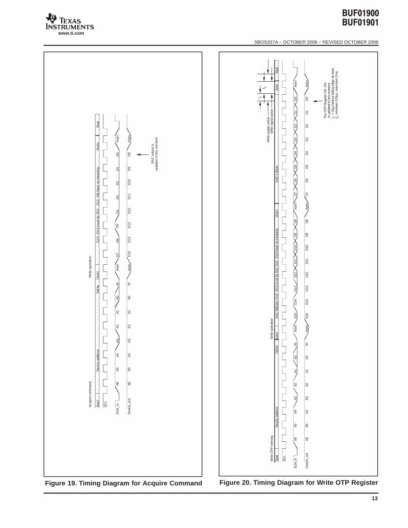
ACQUIRE OF OTP MEMORYAn acquire command updates the DAC output to the valuestored in OTP memory. If the OTP memory has not beenprogrammed, the DAC output code is ‘0000000000’.
Figure 19 shows the timing diagram for the acquirecommand.
Acquire Command
1. Send a START condition on the bus.
2. Send the device address and read/write bit = LOW.The device will acknowledge this byte.
3. Send the acquire command. Bits D7—D5 must beset to 001. Bits D4—D0 do not have meaning. Thisbyte will be acknowledged.
4. Send a STOP condition on the bus.
Writing OTP MemoryThe BUF0190x is able to write to the OTP memory a maxi-mum of four times. Writing to the OTP memory a fourthtime uses all available memory and disables the ability toperform additional writes (see table 3). A reset or acquirecommand updates the DAC output to the most recentlywritten OTP memory value.
When programming the OTP memory, the analog supplyvoltage must be between 8.5V and 18V.
Write commands are performed by setting the read/writebit LOW.
To write to OTP memory:1. Send a START condition on the bus.
2. Send the device address and read/write bit = LOW.The BUF0190x acknowledges this byte.
3. Send two bytes of data for the OTP memory. Begin bysending the most significant byte first (bits D15—D8,of which only bits D9 and D8 are data bits, and bitsD15—D13 must be 010), followed by the leastsignificant byte (bits D7—D0). The register updatesafter receiving the second byte.
4. Send a STOP condition on the bus.
The BUF0190x acknowledges each data byte. If the mas-ter terminates communication early by sending a STOP orSTART condition on the bus, the specified OTP registerwill not be updated. Writing an OTP register updates theDAC output voltage.
Programming timing is taken from the two-wire bus.Therefore, the master must provide correct timing on thebus to ensure data is successfully written into OTPmemory. Figure 20 shows the timing requirements for tim-ing when the OTP write supply and OTP write signal areactive.

"#$%&$$"#$%&$%
SBOS337A − OCTOBER 2006 − REVISED OCTOBER 2006
www.ti.com
12
Writ
eD
ACR
egis
ter.
Writ
eop
erat
ion
Sta
rtD
evic
ead
dres
sW
rite
Ackn
DA
CM
Sby
te.D
15−D
13=
’000
’D12
−D10
have
nom
eani
ng.
Ack
n
SC
L
SD
A_i
nA6
A5
A4A3
A2
A1A
0W
Ack
nD
15D
14D
13D
12D
11D
10D
9D
8
Dev
ice_
out
A6A
5A4
A3A
2A1
A0
WA
ckn
D15
D14
D13
D12
D11
D10
D9
D8
DA
CLS
byte
.A
ckn
Stop
Ack
nD
7D
6D
5D
4D
3D
2D
1D
0A
ckn
Ack
nD
7D
6D
5D
4D
3D
2D
1D
0A
ckn
The
entir
eD
AC
Reg
iste
rD9
−D0
isup
date
din
this
mom
ent.
Figure 17. Timing Diagram for Write DAC Register
Rea
dD
ACR
egis
ter.
Rea
dop
erat
ion
Sta
rtD
evic
ead
dres
sW
rite
Ackn
DA
CM
Sby
te.D
15−D
12sh
owth
epr
ogra
mst
atus
.A
ckn
SC
L
SD
A_in
A6
A5
A4
A3
A2
A1
A0R
Ack
nD
15D
14D
13D
12D
11D
10D
9D
8
Dev
ice_
out
A6
A5
A4
A3
A2
A1
A0R
Ack
nD
15D
14D
13D
12D
11D
10D
9D
8
CO
DE
OTP
Pro
gram
min
gS
tatu
s00
00O
TPha
sno
tbee
npr
ogra
mm
ed00
01O
TPha
sbe
enpr
ogra
mm
edon
ce00
11O
TPha
sbe
enpr
ogra
mm
edtw
ice.
0111
OTP
has
been
prog
ram
med
thre
etim
es.
1111
OTP
has
been
prog
ram
med
four
times
.
DA
CLS
byte
.N
oA
ckn
Sto
p
Ack
nD
7D
6D
5D
4D
3D
2D
1D
0
Ack
nD
7D
6D
5D
4D
3D
2D
1D
0N
oA
ckn
Figure 18. Timing Diagram for Read DAC Register
"#$%&$$"#$%&$%
SBOS337A − OCTOBER 2006 − REVISED OCTOBER 2006
www.ti.com
13
Acq
uire
com
man
d.W
rite
oper
atio
n
Sta
rtD
evic
ead
dres
sW
rite
Ack
nD
15−D
13m
ustb
e’0
01’.
D12
−D8
have
nom
eani
ng.
Ack
nS
top
SC
L
SD
A_i
nA6
A5
A4
A3
A2
A1
A0
WA
ckn
D7
D6
D5
D4
D3
D2
D1
D0
Ack
n
Dev
ice_
out
A6A
5A
4A
3A
2A
1A
0W
Ack
nD
15D
14D
13D
12D
11D
10D
9D
8A
ckn
DA
Cou
tput
isup
date
din
this
mom
ent.
Figure 19. Timing Diagram for Acquire Command
Writ
esu
pply
activ
eW
rite
OTP
mem
ory.
Writ
eop
erat
ion
Writ
esi
gnal
activ
e
Sta
rtD
evic
ead
dres
sW
rite
Ack
nD
AC
MS
byte
.D15
−D13
mus
tbe
010.
D12
−D10
have
nom
eani
ng.
Ack
nD
ACLS
byte
.Ac
knS
top
SC
L
SD
A_i
nA
6A5
A4
A3
A2A
1A
0W
Ack
nD
15D
14D
13D
12D
11D
10D
9D
8A
ckn
D7
D6
D5
D4
D3
D2
D1
D0
Ack
n
Dev
ice_
out
A6
A5A
4A
3A2
A1
A0
WA
ckn
D15
D14
D13
D12
D11
D10
D9
D8
Ack
nD
7D
6D
5D
4D
3D
2D
1D
0A
ckn
The
OTP
Reg
iste
rD9
−D0
isup
date
din
this
mom
ent.
t 1:>
20µs
befo
refa
lling
edge
ofcl
ock.
t 2:m
inim
um10
0 µs,
max
imum
2ms.
t 1t 2
Figure 20. Timing Diagram for Write OTP Register

"#$%&$$"#$%&$%
SBOS337A − OCTOBER 2006 − REVISED OCTOBER 2006
www.ti.com
14
VCOM CALIBRATION
The BUF0190x provides a simple, time- and cost-efficientmeans to adjust the flicker performance of LCD panels ei-ther manually or automatically during the final stages of theLCD panel manufacturing process.
The 10-bit adjustment resolution of the BUF0190x ex-ceeds the typical adjustment resolution of existing VCOMcalibrators significantly. As with a traditional VCOM adjust-ment, which uses a mechanical potentiometer and a volt-age divider for adjustment (see Figure 21), the BUF0190xuses an external voltage divider that is used to set the ini-tial VCOM voltage as well as the adjustment range.
AVDD
RB
RA
RC
VCOM
Figure 21. Traditional V COM Adjustment
As Figure 22 shows, the 10-bit DAC acts as a Rail-to-Railoutput voltage source with a nominal 250kΩ of output im-pedance. For example, at Code 000h, the lowest VCOMvoltage is achieved since the 250kΩ impedance is now inparallel with R2, which lowers the impedance of the lowerside of the voltage divider. Consequently, code 3FFh re-sults in the highest adjustable VCOM voltage.
Once the desired output level is obtained, the part canstore the final setting using the non-volatile on-chipmemory. See Programming section for detailed informa-tion.
VS
R2
R1
VBIASVCOM
(1)
NOTE: (1) Integrated into BUF01900 or external.
(a) Code 00h equivalent circuit.
(b) Code 3FFh equivalent circuit.
250kΩ
BUF0190x
VSVS
R2
R1
VBIASVCOM
(1)250kΩ
BUF0190x
Figure 22. Simplified Block Diagram for V COMAdjustment using BUF0190x
SELECTING THE ADJUSTMENT STEP SIZEA maximum of 1024 adjustment steps can be realized withthe BUF0190x, leading to very high adjustment resolutionand very small step sizes. This flexibility can be advanta-geous during the panel development phase. In a practicalproduction setting, however, this capability might lead toadjustment times that can be too long. A simple solution isto increase the step size between settings to more practi-cal values for mass production. Limiting the number of ad-justment steps between code 000h and code 3FFh to be-tween 16 and 128 has been shown to typically yieldacceptable adjustment results in the smallest amount ofadjustment time.
"#$%&$$"#$%&$%
SBOS337A − OCTOBER 2006 − REVISED OCTOBER 2006
www.ti.com
15
EXTERNAL VOLTAGE DIVIDER RESISTORSELECTIONThe external resistive voltage-divider consisting of R1 andR2 (see Figure 16, Figure 17, and Figure 18) sets both themaximum value of the VCOM adjustment range and the ini-tial VCOM voltage. Follow the steps below to calculate thecorrect values for R1 and R2
Step 1: Choose the supply voltage, (VS)Step 2: Set the nominal VCOM voltage. This voltage is theVCOM voltage at which the unadjusted panel should be atpower-on. The default power-up DAC code is midscale.Step 3: Choose the VCOM adjustment range. The adjust-ment range is the difference between the lowest and thehighest desired VCOM voltage. If the default power-up codeis not overwritten by software at the beginning of the ad-justment cycle, the adjustment range is symmetricalaround the chosen nominal VCOM voltage.Step 4: Calculate the resistors based on the following for-mulas or simply download the Microsoft Excel calculatorlocated in the product folder of BUF0190x available atwww.ti.com.
R1 250k Adj_range
VCOM 0.5 (Adj_range)
R2 1
VSVCOM
1R1
1500k 1
R1 1
250k
CALCULATING THE V COM OUTPUT VOLTAGEWith R1 and R2 properly set, VBIAS or VCOM output voltagecan be calculated for any digital code with the following for-mula:
VCOM 250k R2 VS R1 R2 VS (Code1023)
R1 R2 250k R1 R2
CALCULATING THE ADJUSTMENTRESOLUTIONThe resolution of the adjustment is a function of the stepsize. The resolution can be calculated by simply dividingthe chosen adjustment range by the number of steps:
Resolution = Adj_range/steps (example: 32 steps be-tween code 0h and code 3FFh)
DESIGN EXAMPLE
Step 1: Supply Voltage is 10V.Step 2: Nominal VCOM is determined to be 4V.Step 3: The desired total adjustment range is 1V. In thecase of using the default power-up DAC code (midscale),the adjustment range for the VCOM voltage will be from3.5V to 4.5V.Step 4: Calculation of R1 and R2R1 = 71.4kΩ => choose closest 1% resistor (71.5kΩ)R2 = 45.5kΩ => choose closest 1% resistor (45.3kΩ)Step 5: Appropriate number of adjustment steps betweencode 00h and code 3FFh is determined to be 32. This valueleads to a step size of 32 codes between adjustmentpoints, which translates into approximately 31mV voltagedifference between steps.
MOTOR DRIVE CIRCUITThe BUF01900 can be used to drive small motors directlybecause of the large output drive capability (> 100mA), asillustrated in Figure 23.
BUF01900
VCOM
M
15V
µC
VSD
10kΩ 10kΩ
Figure 23. Motor Drive Circuit
(1)
(2)
(3)

"#$%&$$"#$%&$%
SBOS337A − OCTOBER 2006 − REVISED OCTOBER 2006
www.ti.com
16
PROGRAMMABLE POWER SUPPLY
The BUF0190x integrated buffer amplifier can drive largecapacitive loads (see Typical Characteristics) and greaterthan 100mA of output current, making it well-suited for pro-grammable power supplies.
Note that the BUF01900 integrated buffer has an inputrange that only extends to about 0.8V above GND; there-fore, the programmable power supply is not able to outputvoltages less than approximately 0.8V.
BUF01900
15V
+100µF
Load
3.3V
10kΩ 10kΩ
µC(1)
NOTE: (1) Optional −see Typical Characteristic curvesFigure 10 through Figure 14 for load regulationperformance.
Figure 24. Programmable Power Supply
QFN/DFN THERMALLY-ENHANCEDPACKAGEThe BUF0190x uses the 10-lead DFN package, a thin,thermally-enhanced package designed to eliminate theuse of bulky heat sinks and slugs traditionally used in ther-mal packages. The DFN package can be easily mountedusing standard printed circuit board (PCB) assembly tech-niques. See QFN/SON PCB Attachment Application Note(SLUA271) available at www.ti.com.
The thermal resistance junction to ambient (R JA) of theDFN package depends on the PCB layout. Using thermalvias and wide PCB traces improves thermal resistance.The thermal pad must be soldered to the PCB. The thermalpad on the bottom of the package should be connected toGND.
Soldering the exposed thermal pad significantly improvesboard-level reliability during temperature cycling, keypush, package shear, and similar board-level tests. Evenwith applications that have low-power dissipation, the ex-posed pad must be soldered to the PCB to provide struc-tural integrity and long-term reliability.
PACKAGE OPTION ADDENDUM
www.ti.com 24-Sep-2015
Addendum-Page 1
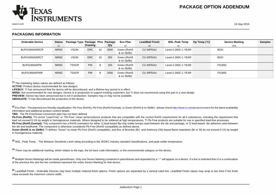
PACKAGING INFORMATION
Orderable Device Status(1)
Package Type PackageDrawing
Pins PackageQty
Eco Plan(2)
Lead/Ball Finish(6)
MSL Peak Temp(3)
Op Temp (°C) Device Marking(4/5)
Samples
BUF01900AIDRCR NRND VSON DRC 10 3000 Green (RoHS& no Sb/Br)
CU NIPDAU Level-2-260C-1 YEAR BOO
BUF01900AIDRCT NRND VSON DRC 10 250 Green (RoHS& no Sb/Br)
CU NIPDAU Level-2-260C-1 YEAR BOO
BUF01900AIPW NRND TSSOP PW 8 150 Green (RoHS& no Sb/Br)
CU NIPDAU Level-2-260C-1 YEAR F01900
BUF01900AIPWR NRND TSSOP PW 8 2000 Green (RoHS& no Sb/Br)
CU NIPDAU Level-2-260C-1 YEAR F01900
(1) The marketing status values are defined as follows:ACTIVE: Product device recommended for new designs.LIFEBUY: TI has announced that the device will be discontinued, and a lifetime-buy period is in effect.NRND: Not recommended for new designs. Device is in production to support existing customers, but TI does not recommend using this part in a new design.PREVIEW: Device has been announced but is not in production. Samples may or may not be available.OBSOLETE: TI has discontinued the production of the device.
(2) Eco Plan - The planned eco-friendly classification: Pb-Free (RoHS), Pb-Free (RoHS Exempt), or Green (RoHS & no Sb/Br) - please check http://www.ti.com/productcontent for the latest availabilityinformation and additional product content details.TBD: The Pb-Free/Green conversion plan has not been defined.Pb-Free (RoHS): TI's terms "Lead-Free" or "Pb-Free" mean semiconductor products that are compatible with the current RoHS requirements for all 6 substances, including the requirement thatlead not exceed 0.1% by weight in homogeneous materials. Where designed to be soldered at high temperatures, TI Pb-Free products are suitable for use in specified lead-free processes.Pb-Free (RoHS Exempt): This component has a RoHS exemption for either 1) lead-based flip-chip solder bumps used between the die and package, or 2) lead-based die adhesive used betweenthe die and leadframe. The component is otherwise considered Pb-Free (RoHS compatible) as defined above.Green (RoHS & no Sb/Br): TI defines "Green" to mean Pb-Free (RoHS compatible), and free of Bromine (Br) and Antimony (Sb) based flame retardants (Br or Sb do not exceed 0.1% by weightin homogeneous material)
(3) MSL, Peak Temp. - The Moisture Sensitivity Level rating according to the JEDEC industry standard classifications, and peak solder temperature.
(4) There may be additional marking, which relates to the logo, the lot trace code information, or the environmental category on the device.
(5) Multiple Device Markings will be inside parentheses. Only one Device Marking contained in parentheses and separated by a "~" will appear on a device. If a line is indented then it is a continuationof the previous line and the two combined represent the entire Device Marking for that device.
(6) Lead/Ball Finish - Orderable Devices may have multiple material finish options. Finish options are separated by a vertical ruled line. Lead/Ball Finish values may wrap to two lines if the finishvalue exceeds the maximum column width.
PACKAGE OPTION ADDENDUM
www.ti.com 24-Sep-2015
Addendum-Page 2
Important Information and Disclaimer:The information provided on this page represents TI's knowledge and belief as of the date that it is provided. TI bases its knowledge and belief on informationprovided by third parties, and makes no representation or warranty as to the accuracy of such information. Efforts are underway to better integrate information from third parties. TI has taken andcontinues to take reasonable steps to provide representative and accurate information but may not have conducted destructive testing or chemical analysis on incoming materials and chemicals.TI and TI suppliers consider certain information to be proprietary, and thus CAS numbers and other limited information may not be available for release.
In no event shall TI's liability arising out of such information exceed the total purchase price of the TI part(s) at issue in this document sold by TI to Customer on an annual basis.
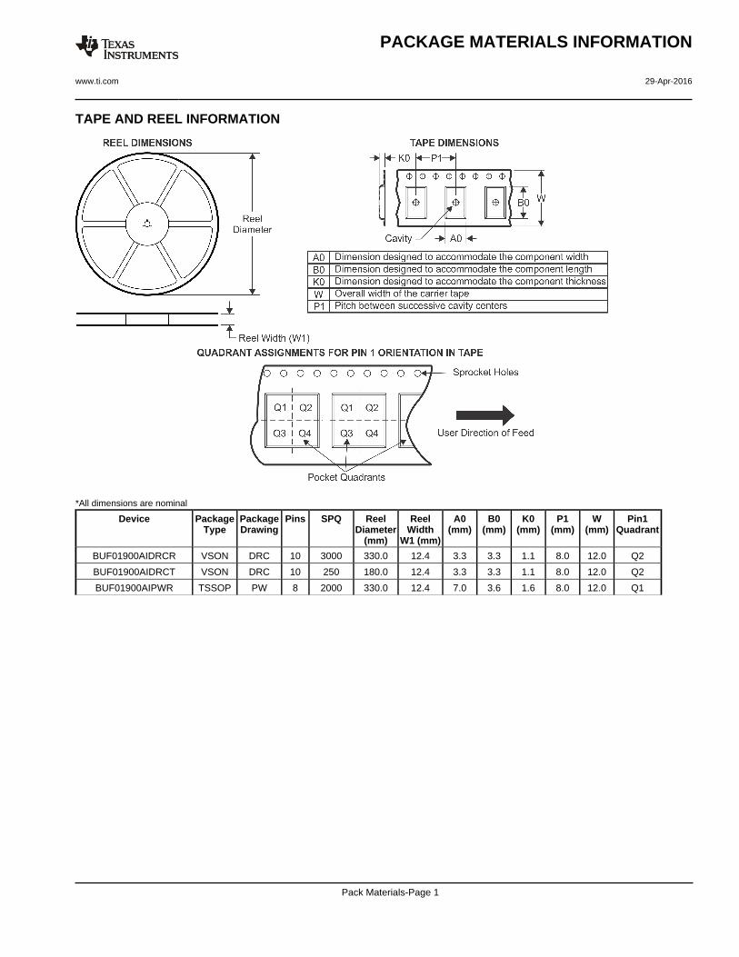
TAPE AND REEL INFORMATION
*All dimensions are nominal
Device PackageType
PackageDrawing
Pins SPQ ReelDiameter
(mm)
ReelWidth
W1 (mm)
A0(mm)
B0(mm)
K0(mm)
P1(mm)
W(mm)
Pin1Quadrant
BUF01900AIDRCR VSON DRC 10 3000 330.0 12.4 3.3 3.3 1.1 8.0 12.0 Q2
BUF01900AIDRCT VSON DRC 10 250 180.0 12.4 3.3 3.3 1.1 8.0 12.0 Q2
BUF01900AIPWR TSSOP PW 8 2000 330.0 12.4 7.0 3.6 1.6 8.0 12.0 Q1
PACKAGE MATERIALS INFORMATION
www.ti.com 29-Apr-2016
Pack Materials-Page 1

*All dimensions are nominal
Device Package Type Package Drawing Pins SPQ Length (mm) Width (mm) Height (mm)
BUF01900AIDRCR VSON DRC 10 3000 367.0 367.0 35.0
BUF01900AIDRCT VSON DRC 10 250 210.0 185.0 35.0
BUF01900AIPWR TSSOP PW 8 2000 367.0 367.0 35.0
PACKAGE MATERIALS INFORMATION
www.ti.com 29-Apr-2016
Pack Materials-Page 2
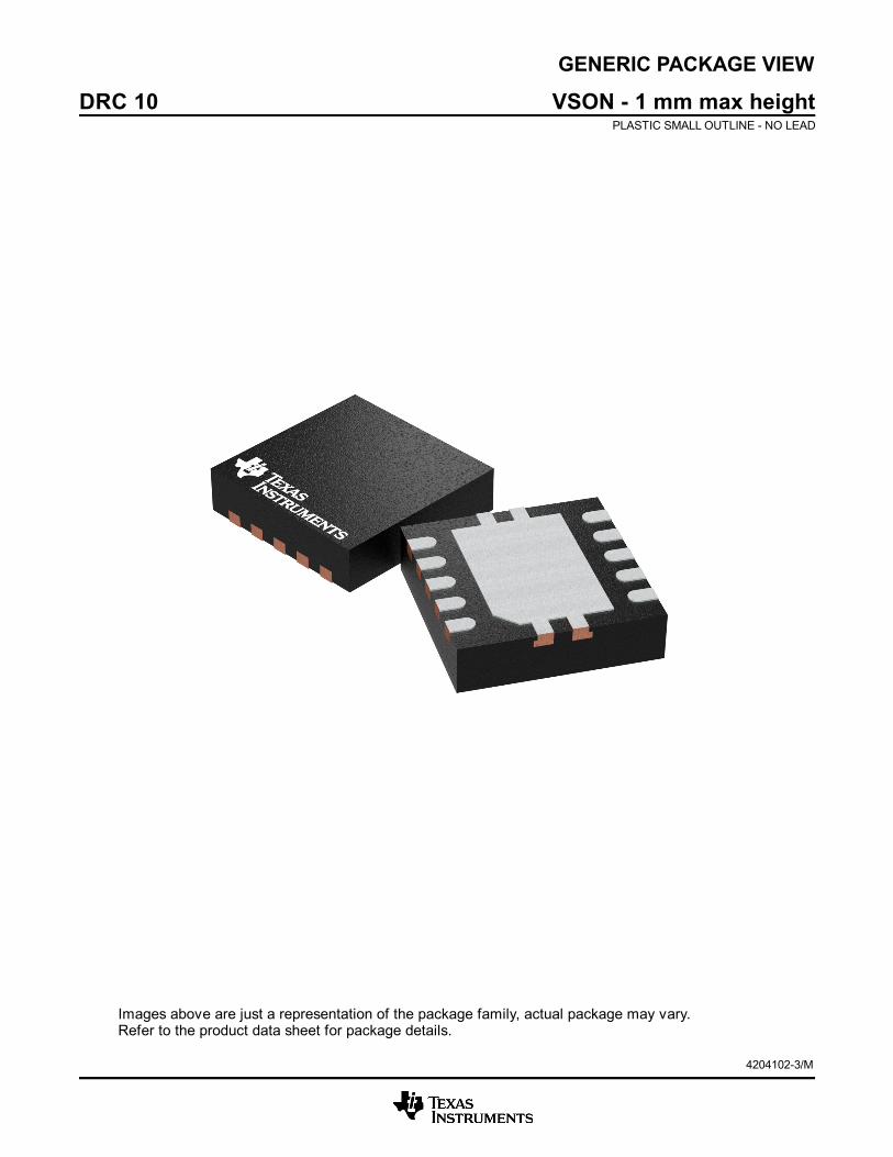
GENERIC PACKAGE VIEW
Images above are just a representation of the package family, actual package may vary.Refer to the product data sheet for package details.
DRC 10 VSON - 1 mm max heightPLASTIC SMALL OUTLINE - NO LEAD
4204102-3/M
www.ti.com
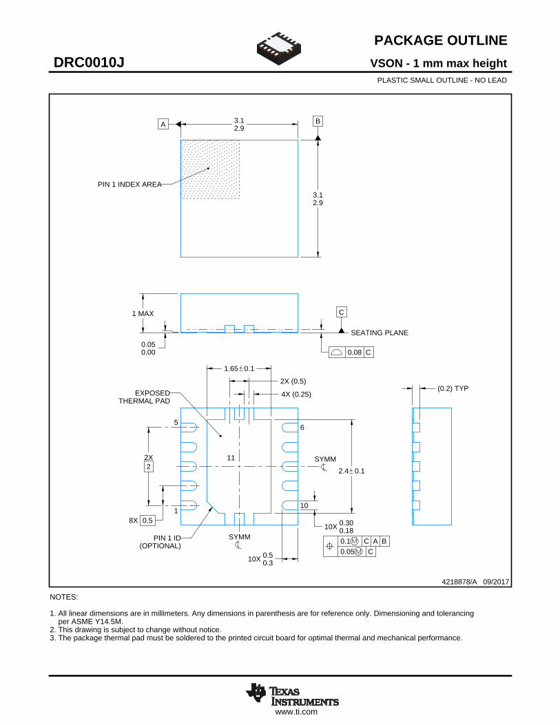
PACKAGE OUTLINE
C
10X 0.300.18
2.4 0.1
2X2
1.65 0.1
8X 0.5
1 MAX
10X 0.50.3
0.050.00
A 3.12.9
B
3.12.9
(0.2) TYP4X (0.25)
2X (0.5)
VSON - 1 mm max heightDRC0010JPLASTIC SMALL OUTLINE - NO LEAD
4218878/A 09/2017
PIN 1 INDEX AREA
SEATING PLANE
0.08 C
1
56
10
(OPTIONAL)PIN 1 ID 0.1 C A B
0.05 C
THERMAL PADEXPOSED
SYMM
SYMM11
NOTES: 1. All linear dimensions are in millimeters. Any dimensions in parenthesis are for reference only. Dimensioning and tolerancing per ASME Y14.5M. 2. This drawing is subject to change without notice. 3. The package thermal pad must be soldered to the printed circuit board for optimal thermal and mechanical performance.
SCALE 4.000

www.ti.com
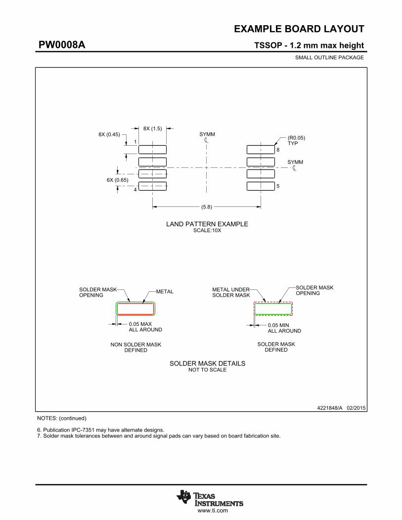
EXAMPLE BOARD LAYOUT
0.07 MINALL AROUND
10X (0.25)
(2.4)
(2.8)
8X (0.5)
(1.65)
( 0.2) VIATYP
(0.575)
(0.95)
10X (0.6)
(R0.05) TYP
(3.4)
4X (0.25)
(0.5)
VSON - 1 mm max heightDRC0010JPLASTIC SMALL OUTLINE - NO LEAD
4218878/A 09/2017
SYMM
1
5 6
10
LAND PATTERN EXAMPLEEXPOSED METAL SHOWN
SCALE:20X
11SYMM
METAL UNDERSOLDER MASK
SOLDER MASKOPENING
NOTES: (continued) 4. This package is designed to be soldered to a thermal pad on the board. For more information, see Texas Instruments literature number SLUA271 (www.ti.com/lit/slua271).5. Vias are optional depending on application, refer to device data sheet. If any vias are implemented, refer to their locations shown on this view. It is recommended that vias under paste be filled, plugged or tented.

www.ti.com
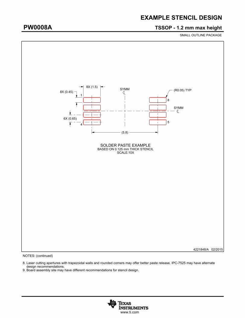
EXAMPLE STENCIL DESIGN
(R0.05) TYP
10X (0.25)
10X (0.6)
2X (1.5)
2X(1.06)
(2.8)
(0.63)
8X (0.5)
(0.5)
4X (0.34)
4X (0.25)
(1.53)
VSON - 1 mm max heightDRC0010JPLASTIC SMALL OUTLINE - NO LEAD
4218878/A 09/2017
NOTES: (continued) 6. Laser cutting apertures with trapezoidal walls and rounded corners may offer better paste release. IPC-7525 may have alternate design recommendations.
SOLDER PASTE EXAMPLEBASED ON 0.125 mm THICK STENCIL
EXPOSED PAD 11:
80% PRINTED SOLDER COVERAGE BY AREASCALE:25X
SYMM
1
56
10
EXPOSED METALTYP
11
SYMM
SOLDER MASK OPENING
METAL UNDERSOLDER MASK

www.ti.com
PACKAGE OUTLINE
C
TYP6.66.2
1.2 MAX
6X 0.65
8X 0.300.19
2X1.95
0.150.05
(0.15) TYP
0 - 8
0.25GAGE PLANE
0.750.50
A
NOTE 3
3.12.9
BNOTE 4
4.54.3
4221848/A 02/2015
TSSOP - 1.2 mm max heightPW0008ASMALL OUTLINE PACKAGE
NOTES: 1. All linear dimensions are in millimeters. Any dimensions in parenthesis are for reference only. Dimensioning and tolerancing per ASME Y14.5M. 2. This drawing is subject to change without notice. 3. This dimension does not include mold flash, protrusions, or gate burrs. Mold flash, protrusions, or gate burrs shall not exceed 0.15 mm per side. 4. This dimension does not include interlead flash. Interlead flash shall not exceed 0.25 mm per side.5. Reference JEDEC registration MO-153, variation AA.
18
0.1 C A B
54
PIN 1 IDAREA
SEATING PLANE
0.1 C
SEE DETAIL A
DETAIL ATYPICAL
SCALE 2.800
www.ti.com
EXAMPLE BOARD LAYOUT
(5.8)
0.05 MAXALL AROUND
0.05 MINALL AROUND
8X (1.5)8X (0.45)
6X (0.65)
(R )TYP
0.05
4221848/A 02/2015
TSSOP - 1.2 mm max heightPW0008ASMALL OUTLINE PACKAGE
SYMM
SYMM
LAND PATTERN EXAMPLESCALE:10X
1
45
8
NOTES: (continued) 6. Publication IPC-7351 may have alternate designs. 7. Solder mask tolerances between and around signal pads can vary based on board fabrication site.
METALSOLDER MASKOPENING
NON SOLDER MASKDEFINED
SOLDER MASK DETAILSNOT TO SCALE
SOLDER MASKOPENING
METAL UNDERSOLDER MASK
SOLDER MASKDEFINED
www.ti.com
EXAMPLE STENCIL DESIGN
(5.8)
6X (0.65)
8X (0.45)8X (1.5)
(R ) TYP0.05
4221848/A 02/2015
TSSOP - 1.2 mm max heightPW0008ASMALL OUTLINE PACKAGE
NOTES: (continued) 8. Laser cutting apertures with trapezoidal walls and rounded corners may offer better paste release. IPC-7525 may have alternate design recommendations. 9. Board assembly site may have different recommendations for stencil design.
SYMM
SYMM
1
45
8
SOLDER PASTE EXAMPLEBASED ON 0.125 mm THICK STENCIL
SCALE:10X
IMPORTANT NOTICE
Texas Instruments Incorporated (TI) reserves the right to make corrections, enhancements, improvements and other changes to itssemiconductor products and services per JESD46, latest issue, and to discontinue any product or service per JESD48, latest issue. Buyersshould obtain the latest relevant information before placing orders and should verify that such information is current and complete.TI’s published terms of sale for semiconductor products (http://www.ti.com/sc/docs/stdterms.htm) apply to the sale of packaged integratedcircuit products that TI has qualified and released to market. Additional terms may apply to the use or sale of other types of TI products andservices.Reproduction of significant portions of TI information in TI data sheets is permissible only if reproduction is without alteration and isaccompanied by all associated warranties, conditions, limitations, and notices. TI is not responsible or liable for such reproduceddocumentation. Information of third parties may be subject to additional restrictions. Resale of TI products or services with statementsdifferent from or beyond the parameters stated by TI for that product or service voids all express and any implied warranties for theassociated TI product or service and is an unfair and deceptive business practice. TI is not responsible or liable for any such statements.Buyers and others who are developing systems that incorporate TI products (collectively, “Designers”) understand and agree that Designersremain responsible for using their independent analysis, evaluation and judgment in designing their applications and that Designers havefull and exclusive responsibility to assure the safety of Designers' applications and compliance of their applications (and of all TI productsused in or for Designers’ applications) with all applicable regulations, laws and other applicable requirements. Designer represents that, withrespect to their applications, Designer has all the necessary expertise to create and implement safeguards that (1) anticipate dangerousconsequences of failures, (2) monitor failures and their consequences, and (3) lessen the likelihood of failures that might cause harm andtake appropriate actions. Designer agrees that prior to using or distributing any applications that include TI products, Designer willthoroughly test such applications and the functionality of such TI products as used in such applications.TI’s provision of technical, application or other design advice, quality characterization, reliability data or other services or information,including, but not limited to, reference designs and materials relating to evaluation modules, (collectively, “TI Resources”) are intended toassist designers who are developing applications that incorporate TI products; by downloading, accessing or using TI Resources in anyway, Designer (individually or, if Designer is acting on behalf of a company, Designer’s company) agrees to use any particular TI Resourcesolely for this purpose and subject to the terms of this Notice.TI’s provision of TI Resources does not expand or otherwise alter TI’s applicable published warranties or warranty disclaimers for TIproducts, and no additional obligations or liabilities arise from TI providing such TI Resources. TI reserves the right to make corrections,enhancements, improvements and other changes to its TI Resources. TI has not conducted any testing other than that specificallydescribed in the published documentation for a particular TI Resource.Designer is authorized to use, copy and modify any individual TI Resource only in connection with the development of applications thatinclude the TI product(s) identified in such TI Resource. NO OTHER LICENSE, EXPRESS OR IMPLIED, BY ESTOPPEL OR OTHERWISETO ANY OTHER TI INTELLECTUAL PROPERTY RIGHT, AND NO LICENSE TO ANY TECHNOLOGY OR INTELLECTUAL PROPERTYRIGHT OF TI OR ANY THIRD PARTY IS GRANTED HEREIN, including but not limited to any patent right, copyright, mask work right, orother intellectual property right relating to any combination, machine, or process in which TI products or services are used. Informationregarding or referencing third-party products or services does not constitute a license to use such products or services, or a warranty orendorsement thereof. Use of TI Resources may require a license from a third party under the patents or other intellectual property of thethird party, or a license from TI under the patents or other intellectual property of TI.TI RESOURCES ARE PROVIDED “AS IS” AND WITH ALL FAULTS. TI DISCLAIMS ALL OTHER WARRANTIES ORREPRESENTATIONS, EXPRESS OR IMPLIED, REGARDING RESOURCES OR USE THEREOF, INCLUDING BUT NOT LIMITED TOACCURACY OR COMPLETENESS, TITLE, ANY EPIDEMIC FAILURE WARRANTY AND ANY IMPLIED WARRANTIES OFMERCHANTABILITY, FITNESS FOR A PARTICULAR PURPOSE, AND NON-INFRINGEMENT OF ANY THIRD PARTY INTELLECTUALPROPERTY RIGHTS. TI SHALL NOT BE LIABLE FOR AND SHALL NOT DEFEND OR INDEMNIFY DESIGNER AGAINST ANY CLAIM,INCLUDING BUT NOT LIMITED TO ANY INFRINGEMENT CLAIM THAT RELATES TO OR IS BASED ON ANY COMBINATION OFPRODUCTS EVEN IF DESCRIBED IN TI RESOURCES OR OTHERWISE. IN NO EVENT SHALL TI BE LIABLE FOR ANY ACTUAL,DIRECT, SPECIAL, COLLATERAL, INDIRECT, PUNITIVE, INCIDENTAL, CONSEQUENTIAL OR EXEMPLARY DAMAGES INCONNECTION WITH OR ARISING OUT OF TI RESOURCES OR USE THEREOF, AND REGARDLESS OF WHETHER TI HAS BEENADVISED OF THE POSSIBILITY OF SUCH DAMAGES.Unless TI has explicitly designated an individual product as meeting the requirements of a particular industry standard (e.g., ISO/TS 16949and ISO 26262), TI is not responsible for any failure to meet such industry standard requirements.Where TI specifically promotes products as facilitating functional safety or as compliant with industry functional safety standards, suchproducts are intended to help enable customers to design and create their own applications that meet applicable functional safety standardsand requirements. Using products in an application does not by itself establish any safety features in the application. Designers mustensure compliance with safety-related requirements and standards applicable to their applications. Designer may not use any TI products inlife-critical medical equipment unless authorized officers of the parties have executed a special contract specifically governing such use.Life-critical medical equipment is medical equipment where failure of such equipment would cause serious bodily injury or death (e.g., lifesupport, pacemakers, defibrillators, heart pumps, neurostimulators, and implantables). Such equipment includes, without limitation, allmedical devices identified by the U.S. Food and Drug Administration as Class III devices and equivalent classifications outside the U.S.TI may expressly designate certain products as completing a particular qualification (e.g., Q100, Military Grade, or Enhanced Product).Designers agree that it has the necessary expertise to select the product with the appropriate qualification designation for their applicationsand that proper product selection is at Designers’ own risk. Designers are solely responsible for compliance with all legal and regulatoryrequirements in connection with such selection.Designer will fully indemnify TI and its representatives against any damages, costs, losses, and/or liabilities arising out of Designer’s non-compliance with the terms and provisions of this Notice.
Mailing Address: Texas Instruments, Post Office Box 655303, Dallas, Texas 75265Copyright © 2018, Texas Instruments Incorporated