Embed Size (px)
Citation preview
ProFLEX01-R2 Transceiver Module
Datasheet
The information in this document is subject to change without notice. 330-0098-R4.0 Copyright © 2012-2017 LSR Page 1 of 47
Integrated Transceiver Modules for ZigBee / 802.15.4 (2.4 GHz)
Development Kit Available
FEATURES
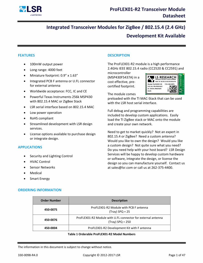
• 100mW output power
• Long range: 4000 feet
• Miniature footprint: 0.9” x 1.63”
• Integrated PCB F antenna or U.FL connector for external antenna
• Worldwide acceptance: FCC, IC and CE
• Powerful Texas Instruments 256k MSP430 with 802.15.4 MAC or ZigBee Stack
• LSR serial interface based on 802.15.4 MAC
• Low power operation
• RoHS compliant
• Streamlined development with LSR design services.
• License options available to purchase design or integrate design.
APPLICATIONS
• Security and Lighting Control
• HVAC Control
• Sensor Networks
• Medical
• Smart Energy
DESCRIPTION
The ProFLEX01-R2 module is a high performance 2.4GHz IEEE 802.15.4 radio (CC2520 & CC2591) and microcontroller (MSP430F5437A) in a cost effective, pre-certified footprint.
The module comes preloaded with the TI MAC-Stack that can be used with the LSR host serial interface.
Full debug and programming capabilities are included to develop custom applications. Easily load the TI ZigBee stack or MAC onto the module and create your own network.
Need to get to market quickly? Not an expert in 802.15.4 or ZigBee? Need a custom antenna? Would you like to own the design? Would you like a custom design? Not quite sure what you need? Do you need help with your host board? LSR Design Services will be happy to develop custom hardware or software, integrate the design, or license the design so you can manufacture yourself. Contact us at [email protected] or call us at 262-375-4400.
ORDERING INFORMATION
Order Number Description
450-0075 ProFLEX01-R2 Module with PCB F antenna
(Tray) SPQ = 25
450-0076 ProFLEX01-R2 Module with U.FL connector for external antenna
(Tray) SPQ = 250
450-0004 ProFLEX01-R2 Development Kit with F antenna
Table 1 Orderable ProFLEX01-R2 Model Numbers

ProFLEX01-R2 Transceiver Module
Datasheet
The information in this document is subject to change without notice. 330-0098-R4.0 Copyright © 2012-2017 LSR Page 2 of 47
MODULE ACCESSORIES
Order Number Description
001-0001 2.4 GHz Dipole Antenna with Reverse Polarity
SMA Connector
001-0010 2.4 GHz Waterproof Dipole Antenna with
Reverse Polarity SMA Connector
080-0001 U.FL to Reverse Polarity SMA Bulkhead Cable
105mm
080-0013 Waterproof U.FL to Reverse Polarity SMA
Bulkhead Cable, O-Ring Seal, 105mm
080-0014 Waterproof U.FL to Reverse Polarity SMA
Bulkhead Cable, O-Ring Seal, 210mm

ProFLEX01-R2 Transceiver Module
Datasheet
The information in this document is subject to change without notice. 330-0098-R4.0 Copyright © 2012-2017 LSR Page 3 of 47
BLOCK DIAGRAM
MSP430F5437A
(Microcontroller)
CC2520
(802.15.4 Radio)
CC2591
(PA/LNA)SPI AntennaSerial I/O
An
alo
gG
PIO
PG
M/D
BG
TM
R/P
WM
Figure 1 ProFLEX01-R2 Module Block Diagram – High-Level
DEVELOPMENT KIT
The ProFLEX01-R2 Development Kit can be used out of the box to evaluate RF range performance with the simple press of a button.
Users interested in further investigating the performance and capabilities of the ProFLEX01-R2 Module can use the ProFLEX01-R2 Test Tool. This PC-based software can demonstrate just how easy it is to send & receive data, collect performance data, change channels, power levels, or addresses using the LSR Serial Host Protocol with another microcontroller.
More advanced users can use the development board to create and debug their own software for the ProFLEX01-R2 module using the 802.15.4 MAC or ZigBee stack from TI.
Part Number Description
450-0004 ProFLEX01-R2 Development
Kit with F Antenna
Figure 2 ProFLEX01-R2 Development Board
Kit Contents
• ProFLEX01-R2 Development Board with ProFLEX01-R2 Series Transceiver Module with F antenna (x2)
• USB Cable (x2)
• AA Batteries (x4)
• Quick Start Guide

ProFLEX01-R2 Transceiver Module
Datasheet
The information in this document is subject to change without notice. 330-0098-R4.0 Copyright © 2012-2017 LSR Page 4 of 47
TABLE OF CONTENTS
Development Kit Available .................................................................................................................................. 1
FEATURES ...................................................................................................................................... 1
APPLICATIONS ............................................................................................................................... 1
DESCRIPTION ................................................................................................................................ 1
ORDERING INFORMATION ............................................................................................................ 1
MODULE ACCESSORIES .................................................................................................................. 2
BLOCK DIAGRAM ........................................................................................................................... 3
DEVELOPMENT KIT ........................................................................................................................ 3
Kit Contents ........................................................................................................................................................ 3
MODULE PINOUT AND PIN DESCRIPTIONS .................................................................................... 7
MODULE OVERVIEW ................................................................................................................... 12
Microcontroller ................................................................................................................................................. 12
Radio ................................................................................................................................................................ 13
PA/LNA ............................................................................................................................................................. 15
Antenna Options ............................................................................................................................................... 15
MODES OF OPERATION ............................................................................................................... 17
Host Microcontroller ......................................................................................................................................... 17
Software Stacks ................................................................................................................................................ 18
DEVELOPMENT TOOLS ................................................................................................................ 19
TI MSP-FET430UIF ............................................................................................................................................. 19
IAR Embedded Workbench for MSP430 ............................................................................................................. 19
ELECTRICAL SPECIFICATIONS ....................................................................................................... 20
Absolute Maximum Ratings .............................................................................................................................. 20
Recommended Operating Conditions ................................................................................................................ 20
General Characteristics ..................................................................................................................................... 21
RF Characteristics .............................................................................................................................................. 22
SOLDERING RECOMMENDATIONS ............................................................................................... 25
Recommended Reflow Profile for Lead Free Solder ........................................................................................... 25
ProFLEX01-R2 Transceiver Module
Datasheet
The information in this document is subject to change without notice. 330-0098-R4.0 Copyright © 2012-2017 LSR Page 5 of 47
CLEANING ................................................................................................................................... 26
OPTICAL INSPECTION .................................................................................................................. 26
REWORK ..................................................................................................................................... 26
SHIPPING, HANDLING, AND STORAGE ......................................................................................... 26
Shipping ............................................................................................................................................................ 26
Handling ........................................................................................................................................................... 26
Moisture Sensitivity Level (MSL) ........................................................................................................................ 26
Storage ............................................................................................................................................................. 26
Repeating Reflow Soldering .............................................................................................................................. 27
AGENCY STATEMENTS ................................................................................................................. 28
Agency Certifications ........................................................................................................................................ 28
Federal Communication Commission Interference Statement ............................................................................ 28
Industry Canada Statements ............................................................................................................................. 29
OEM Responsibilities to comply with FCC and Industry Canada Regulations ....................................................... 30
End Product Labelling ........................................................................................................................................ 31
EUROPE ....................................................................................................................................... 32
CE Notice .......................................................................................................................................................... 32
Declaration of Conformity (DoC) ....................................................................................................................... 32
ANTENNA INFORMATION ............................................................................................................ 33
Dipole Antenna 001-0001 .................................................................................................................................. 33
F Antenna ......................................................................................................................................................... 33
MECHANICAL DATA ..................................................................................................................... 42
PCB Footprint .................................................................................................................................................... 42
General Module Dimensions ............................................................................................................................. 43
COMPATIBILITY ........................................................................................................................... 44
MODULE REVISION HISTORY ....................................................................................................... 45
Rev 1 ................................................................................................................................................................ 45

ProFLEX01-R2 Transceiver Module
Datasheet
The information in this document is subject to change without notice. 330-0098-R4.0 Copyright © 2012-2017 LSR Page 6 of 47
LS RESEARCH
MAC ID: 00:25:CA:02:XX:XX:XX:XX
00:25:CA:02:XX:XX:XX = MAC ID
2D Barcode Format is Data Matrix Standard
XX:XX:XX:XX = unique portion of MAC ID that
changes for each module
Wireless Product Development
M/N: ProFLEX01-R2 P/N: 450-0075
RE
V 1 2D
Bar
Code
FCC ID: TFB-PROFLEX1
IC: 5969A-PROFLEX1
RoHS
Part Number: 450-0075
F Antenna Module
Rev 2 .................................................................. 45
Rev 3 ................................................................................................................................................................ 46
Rev 4 ................................................................................................................................................................ 46
CONTACTING LSR ........................................................................................................................ 47

ProFLEX01-R2 Transceiver Module
Datasheet
The information in this document is subject to change without notice. 330-0098-R4.0 Copyright © 2012-2017 LSR Page 7 of 47
MODULE PINOUT AND PIN DESCRIPTIONS
MCU# GND 1
Texas Instruments MSP430F5437A
69 GND MCU#
- GND 2 68 GND -
- GND 3 67 GND -
- NC 4 66 NC -
- NC 5 65 NC -
- NC 6 64 NC -
- NC 7 63 NC -
- NC 8 62 NC -
74 JTAG TMS 9 61 P5.6 56
73 JTAG TDI 10 60 P5.7 57
75 JTAG TCK 11 59 P3.6 41
72 JTAG TDO 12 58 P5.5 55
71 TEST 13 57 P3.7 42
76 nRESET 14 56 P5.4 54
9 P5.0 15 55 P2.4 29
10 P5.1 16 54 P2.3 28
77 P6.0 17 53 P2.2 27
78 P6.1 18 52 P2.1 26
79 P6.2 19 51 P2.0 25
80 P6.3 20 50 P1.1 18
1 P6.4 21 49 P1.0 17
2 P6.5 22 48 P7.7 8
3 P6.6 23 47 P1.2 19
4 P6.7 24 46 P8.0 60
5 P7.4 25 45 P8.1 61
- VCC - 3V3DC 26 44 GND -
27 28 29 30 31 32 33 34 35 36 37 38 39 40 41 42 43
P4
.7
P4
.6
P4
.5
P4
.4
P4
.3
P4
.2
P4
.1
P4
.0
P3
.4/U
AR
T TX
P3
.5/U
AR
T R
X
P7
.2/C
TS
P7
.3
P8
.6
P8
.5
P8
.4
P8
.3
P8
.2
MCU# 53 52 48 47 46 45 44 43 39 40 58 59 66 65 64 63 62 MCU#
Figure 3 Module Pinout
ProFLEX01-R2 Transceiver Module
Datasheet
The information in this document is subject to change without notice. 330-0098-R4.0 Copyright © 2012-2017 LSR Page 8 of 47
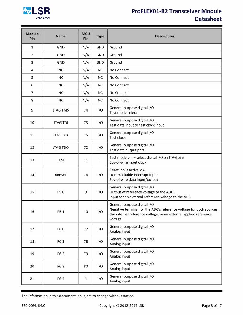
Module Pin
Name MCU Pin
Type Description
1 GND N/A GND Ground
2 GND N/A GND Ground
3 GND N/A GND Ground
4 NC N/A NC No Connect
5 NC N/A NC No Connect
6 NC N/A NC No Connect
7 NC N/A NC No Connect
8 NC N/A NC No Connect
9 JTAG TMS 74 I/O General-purpose digital I/O Test mode select
10 JTAG TDI 73 I/O General-purpose digital I/O Test data input or test clock input
11 JTAG TCK 75 I/O General-purpose digital I/O Test clock
12 JTAG TDO 72 I/O General-purpose digital I/O Test data output port
13 TEST 71 I Test mode pin – select digital I/O on JTAG pins Spy-bi-wire input clock
14 nRESET 76 I/O Reset input active low Non-maskable interrupt input Spy-bi-wire data input/output
15 P5.0 9 I/O General-purpose digital I/O Output of reference voltage to the ADC Input for an external reference voltage to the ADC
16 P5.1 10 I/O
General-purpose digital I/O Negative terminal for the ADC's reference voltage for both sources, the internal reference voltage, or an external applied reference voltage
17 P6.0 77 I/O General-purpose digital I/O Analog input
18 P6.1 78 I/O General-purpose digital I/O Analog input
19 P6.2 79 I/O General-purpose digital I/O Analog input
20 P6.3 80 I/O General-purpose digital I/O Analog input
21 P6.4 1 I/O General-purpose digital I/O Analog input

ProFLEX01-R2 Transceiver Module
Datasheet
The information in this document is subject to change without notice. 330-0098-R4.0 Copyright © 2012-2017 LSR Page 9 of 47
Module Pin
Name MCU Pin
Type Description
22 P6.5 2 I/O General-purpose digital I/O Analog input
23 P6.6 3 I/O General-purpose digital I/O Analog input
24 P6.7 4 I/O General-purpose digital I/O Analog input
25 P7.4 5 I/O General-purpose digital I/O Analog input
26 VCC - 3V3DC VCC VCC Supply Voltage
27 P4.7 53 I/O General-purpose digital I/O Timer_B7 clock input SMCLK output
28 P4.6 52 I/O General-purpose digital I/O Timer_B7 capture CCR6: CCI6A/CCI6B input, compare: Out6 output
29 P4.5 48 I/O General-purpose digital I/O Timer_B7 capture CCR5: CCI5A/CCI5B input, compare: Out5 output
30 P4.4 47 I/O General-purpose digital I/O Timer_B7 capture CCR4: CCI4A/CCI4B input, compare: Out4 output
31 P4.3 46 I/O General-purpose digital I/O Timer_B7 capture CCR3: CCI3A/CCI3B input, compare: Out3 output
32 P4.2 45 I/O General-purpose digital I/O Timer_B7 capture CCR2: CCI2A/CCI2B input, compare: Out2 output
33 P4.1 44 I/O General-purpose digital I/O Timer_B7 capture CCR1: CCI1A/CCI1B input, compare: Out1 output
34 P4.0 43 I/O General-purpose digital I/O Timer_B7 capture CCR0: CCI0A/CCI0B input, compare: Out0 output
35 P3.4/UART TX 39 I/O General-purpose digital I/O Transmit data – USCI_A0 UART mode Slave in, master out – USCI_A0 SPI mode
36 P3.5/UART RX 40 I/O General-purpose digital I/O Receive data – USCI_A0 UART mode Slave out, master in – USCI_A0 SPI mode
37 P7.2 58 I/O General-purpose digital I/O Switch all PWM outputs high impedance – Timer_B SVM output
38 P7.3 59 I/O General-purpose digital I/O Timer1_A3 CCR2 capture: CCI2B input, compare: Out2 output
39 P8.6 66 I/O General-purpose digital I/O Timer1_A3 CCR1 capture: CCI1B input, compare: Out1 output

ProFLEX01-R2 Transceiver Module
Datasheet
The information in this document is subject to change without notice. 330-0098-R4.0 Copyright © 2012-2017 LSR Page 10 of 47
Module Pin
Name MCU Pin
Type Description
40 P8.5 65 I/O General-purpose digital I/O Timer1_A3 CCR0 capture: CCI0B input, compare: Out0 output
41 P8.4 64 I/O General-purpose digital I/O Timer0_A5 CCR4 capture: CCI4B input, compare: Out4 output
42 P8.3 63 I/O General-purpose digital I/O Timer0_A5 CCR3 capture: CCI3B input, compare: Out3 output
43 P8.2 62 I/O General-purpose digital I/O Timer0_A5 CCR2 capture: CCI2B input, compare: Out2 output
44 GND N/A GND Ground
45 P8.1 61 I/O General-purpose digital I/O Timer0_A5 CCR1 capture: CCI1B input, compare: Out1 output
46 P8.0 60 I/O General-purpose digital I/O Timer0_A5 CCR0 capture: CCI0B input, compare: Out0 output
47 P1.2 19 I/O General-purpose digital I/O with port interrupt TA0 CCR1 capture: CCI1A input, compare: Out1 output BSL receive input
48 P7.7 8 I/O General-purpose digital I/O Analog input
49 P1.0 17 I/O General-purpose digital I/O with port interrupt Timer0_A5 clock signal TACLK input ACLK output
50 P1.1 18 I/O General-purpose digital I/O with port interrupt Timer0_A5 CCR0 capture: CCI0A input, compare: Out0 output BSL transmit output
51 P2.0 25 I/O General-purpose digital I/O with port interrupt Timer1_A3 clock signal TA1CLK input MCLK output
52 P2.1 26 I/O General-purpose digital I/O with port interrupt Timer1_A3 CCR0 capture: CCI0A input, compare: Out0 output
53 P2.2 27 I/O General-purpose digital I/O with port interrupt Timer1_A3 CCR1 capture: CCI1A input, compare: Out1 output
54 P2.3 28 I/O General-purpose digital I/O with port interrupt Timer1_A3 CCR2 capture: CCI2A input, compare: Out2 output
55 P2.4 29 I/O General-purpose digital I/O with port interrupt RTCCLK output
56 P5.4 54 I/O General-purpose digital I/O Slave out, master in – USCI_B1 SPI mode I2C clock – USCI_B1 I2C mode
ProFLEX01-R2 Transceiver Module
Datasheet
The information in this document is subject to change without notice. 330-0098-R4.0 Copyright © 2012-2017 LSR Page 11 of 47
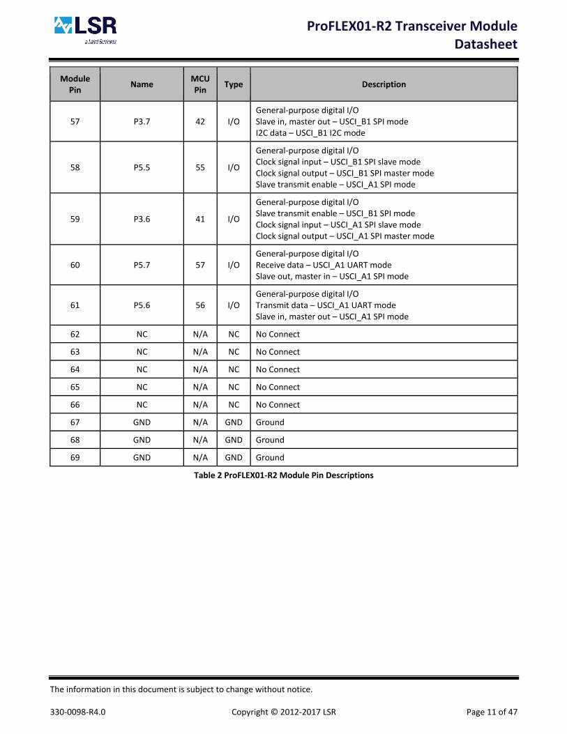
Module Pin
Name MCU Pin
Type Description
57 P3.7 42 I/O General-purpose digital I/O Slave in, master out – USCI_B1 SPI mode I2C data – USCI_B1 I2C mode
58 P5.5 55 I/O
General-purpose digital I/O Clock signal input – USCI_B1 SPI slave mode Clock signal output – USCI_B1 SPI master mode Slave transmit enable – USCI_A1 SPI mode
59 P3.6 41 I/O
General-purpose digital I/O Slave transmit enable – USCI_B1 SPI mode Clock signal input – USCI_A1 SPI slave mode Clock signal output – USCI_A1 SPI master mode
60 P5.7 57 I/O General-purpose digital I/O Receive data – USCI_A1 UART mode Slave out, master in – USCI_A1 SPI mode
61 P5.6 56 I/O General-purpose digital I/O Transmit data – USCI_A1 UART mode Slave in, master out – USCI_A1 SPI mode
62 NC N/A NC No Connect
63 NC N/A NC No Connect
64 NC N/A NC No Connect
65 NC N/A NC No Connect
66 NC N/A NC No Connect
67 GND N/A GND Ground
68 GND N/A GND Ground
69 GND N/A GND Ground
Table 2 ProFLEX01-R2 Module Pin Descriptions

ProFLEX01-R2 Transceiver Module
Datasheet
The information in this document is subject to change without notice. 330-0098-R4.0 Copyright © 2012-2017 LSR Page 12 of 47
MODULE OVERVIEW
Figure 4 shows the internal interconnects of the ICs on the ProFLEX01-R2 module. Consult the respective IC datasheets for details, or contact LSR sales to purchase the ProFLEX01-R2 module schematics as part of LSR’s ModFLEX™ design program. For a high-level block diagram of the ProFLEX01-R2 module, see Figure 1.
Texas Instruments
MSP430F5437A
Texas Instruments
CC2520
/RF_RST
CC_GPIO0
CC_GPIO2
SO
SI
/CS
VREG_EN
CC_GPIO1
SCLK
Texas Instruments
CC2591
HGM
LNA_EN
PA_EN
MurataLDB182G4520C-110
RF_N
RF
_P
RF
_N
7
7
6
5
2
4
6
5
4
4619
2
28
1
3
26
7
9
10
25
38
37
36
35
24
23
22
21
1
Figure 4 ProFLEX01-R2 Module Block Diagram – Internal Interconnects
Microcontroller
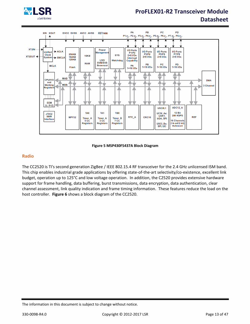
A member of the Texas Instruments MSP430 family of ultra-low-power microcontrollers, the architecture, combined with five low-power modes, is optimized to achieve extended battery life. The device features a powerful 16-bit RISC CPU, 16-bit registers, and constant generators that contribute to maximum code efficiency. The digitally controlled oscillator (DCO) allows wake-up from low-power modes to active mode in less than 5 µs. It can be configured to use up to three 16-bit timers, a high performance 12-bit analog-to-digital (A/D) converter, up to four universal serial communication interfaces (USCI), hardware multiplier, DMA, real time clock module with alarm capabilities, and up to 87 I/O pins. Figure 5 shows a block diagram of the MSP430F5437A.
ProFLEX01-R2 Transceiver Module
Datasheet
The information in this document is subject to change without notice. 330-0098-R4.0 Copyright © 2012-2017 LSR Page 13 of 47
Figure 5 MSP430F5437A Block Diagram
Radio
The CC2520 is TI's second generation ZigBee / IEEE 802.15.4 RF transceiver for the 2.4 GHz unlicensed ISM band. This chip enables industrial grade applications by offering state-of-the-art selectivity/co-existence, excellent link budget, operation up to 125°C and low voltage operation. In addition, the C2520 provides extensive hardware support for frame handling, data buffering, burst transmissions, data encryption, data authentication, clear channel assessment, link quality indication and frame timing information. These features reduce the load on the host controller. Figure 6 shows a block diagram of the CC2520.

ProFLEX01-R2 Transceiver Module
Datasheet
The information in this document is subject to change without notice. 330-0098-R4.0 Copyright © 2012-2017 LSR Page 14 of 47
Figure 6 CC2520 Block Diagram

ProFLEX01-R2 Transceiver Module
Datasheet
The information in this document is subject to change without notice. 330-0098-R4.0 Copyright © 2012-2017 LSR Page 15 of 47
PA/LNA
The CC2591 is a cost-effective and high performance RF Front End for low-power and low-voltage 2.4-GHz wireless applications. It is a range extender for all existing and future 2.4-GHz low-power RF transceivers, transmitters and System-on-Chip products from Texas Instruments. It increases the link budget by providing a power amplifier for increased output power, and a LNA with low noise figure for improved receiver sensitivity. It provides a small size, high output power RF design with its 4x4-mm QFN-16 package. It contains PA, LNA, switches, RF-matching, and balun for simple design of high performance wireless applications. Figure 7 shows a block diagram of the CC2591.
Figure 7 CC2591 Block Diagram
Antenna Options
The ProFLEX01-R2 module includes an integrated PCB F-antenna. An optional configuration with a U.FL connector is also available. The module regulatory certification has been completed with the following antennas:
• PCB trace antenna • LSR 001-0001 2.4 GHz Dipole Antenna with Reverse Polarity SMA Connector and LSR 080-0001 U.FL to Reverse
Polarity SMA Bulkhead Cable 105mm
• Nearson S131CL-6-PX-2450S dipole antenna on a 6 inch cable with connectors.
An adequate ground plane is necessary to provide good efficiency. The ground plane of the host board on which the module is mounted increases the effective antenna ground plane size and improves the antenna performance.
The environment the module is placed in will dictate the range performance. The non-ideal characteristics of the environment will result in the transmitted signal being reflected, diffracted, and scattered. All of these factors randomly combine to create extremely complex scenarios that will affect the link range in various ways.

ProFLEX01-R2 Transceiver Module
Datasheet
The information in this document is subject to change without notice. 330-0098-R4.0 Copyright © 2012-2017 LSR Page 16 of 47
It is also best to keep some clearance between the antenna and nearby objects. This includes how the module is mounted in the product enclosure. Unless the items on the following list of recommendations are met, the radiation pattern can be heavily distorted.
Whichever antennas are used, it is best to keep a few things in mind when determining their location.
• Never place ground plane or copper trace routing underneath the antenna.
• LSR recommends keeping metal objects as far away from the antenna as possible. At a very minimum keep the antennas at least 16mm from any metallic objects, components, or wiring. The farther the antenna is placed from these interferers, the less the radiation pattern and gain will be perturbed
• Do not embed the antenna in a metallic or metalized plastic enclosure.
• Try to keep any plastic enclosure greater than 1 cm from the antenna in any orientation.

ProFLEX01-R2 Transceiver Module
Datasheet
The information in this document is subject to change without notice. 330-0098-R4.0 Copyright © 2012-2017 LSR Page 17 of 47
MODES OF OPERATION
• With a host microcontroller
• With the TI 802.15.4 MAC, ZigBee stack, RF4CE stack, and SimpliciTI
Host Microcontroller
Pro-FLEX Module on
Evaluation BoardUART
PC
LSR Test Tool
Software
Pro-FLEX Module on
Your Board
Your Microcontroller
(Host) of Choice UART
-OR-
Figure 8 Host Microcontroller Modes of Operation
Out of the box the ProFLEX01-R2 module contains an 802.15.4 based application that uses a host serial processor. This allows features of the module to be explored with the LSR PC based test tool, or controlled with a host microcontroller. The advantage of this method is simplicity; all major features of using the radio are simplified into a simple serial message, taking the burden of becoming a radio expert off the developer.
Use the Communications Log in the ModFLEX™ Test Tool Suite software and serial host protocol documents to see the messages in action. It will help you become familiar with the serial commands and how to implement them on your own microcontroller.
Figure 9 ModFLEX™ Test Tool Communications Log
Some examples of serial commands that can be used with the ProFLEX01-R2 Module:
• Set/Query RF channel
• Set/Query RF power
• Set/Query device address
• Transmit RF data or notification RF data received
• Go to Sleep

ProFLEX01-R2 Transceiver Module
Datasheet
The information in this document is subject to change without notice. 330-0098-R4.0 Copyright © 2012-2017 LSR Page 18 of 47
Software Stacks
There are several software stacks provided by TI to streamline development, two of which are described below:
MAC (802.15.4)
Z-Stack (Zigbee)
Overall Complexity and Development Effort
Figure 10 ProFLEX01-R2 Compatible Stacks
802.15.4 MAC
• Use for applications requiring point-to-point or star network topology.
• Advantages: Quick learning curve, minimize software development, easy to deploy in the field
• Disadvantages: No mesh networking
802.15.4 MAC
(To Tx/Rx RF data)
Application Software
(to control switches,
LED’s, serial ports
and so on)
Software
Interface
Figure 11 ProFLEX01-R2 with 802.15.4 MAC
TI Z-Stack (ZigBee)
• Use when mesh networking is required.
• Advantages: Covers a large area with a ZigBee network.
• Disadvantages: Large learning curve, more software development, and complexity
Application Software
(to control switches,
LED’s, serial ports
and so on)
Software
Interface
Z-Stack (ZigBee)
(To Tx/Rx RF data)
Figure 12 ProFLEX01-R2 with TI Z-Stack (ZigBee)

ProFLEX01-R2 Transceiver Module
Datasheet
The information in this document is subject to change without notice. 330-0098-R4.0 Copyright © 2012-2017 LSR Page 19 of 47
DEVELOPMENT TOOLS
TI MSP-FET430UIF
Custom firmware development can be done on the ProFLEX01-R2 module using development tools available thought TI. Shown in Figure 13, a MSP-FETUIF USB interface is required. It plugs directly into the ProFLEX01-R2 Development Board (see Figure 2), and can easily be adapted to other hardware. See the Texas Instruments website for more information.
Figure 13 MSP-FET430UIF
IAR Embedded Workbench for MSP430
Also required is Embedded Workbench for TI MSP430 from IAR Systems. IAR Embedded Workbench for MSP430 is an integrated development environment for building and debugging embedded applications. Visit the IAR Systems website for additional information.
ProFLEX01-R2 Transceiver Module
Datasheet
The information in this document is subject to change without notice. 330-0098-R4.0 Copyright © 2012-2017 LSR Page 20 of 47
ELECTRICAL SPECIFICATIONS
The majority of these characteristics are based on the use of the TI 802.15.4 MAC loaded with the generic application firmware written by LSR. Custom firmware may require these values to be re-characterized by the customer.
Absolute Maximum Ratings
Parameter Min Max Unit
Power supply voltage (VCC) -0.2 +3.6 V
Voltage on any GPIO -0.2 VCC + 0.2 V
RF input power, antenna port +10 dBm
RF input power, transmit port +8 dBm
Operating temperature -40 +85 ºC
Storage temperature -40 +105 ºC
Table 3 Absolute Maximum Ratings1
Recommended Operating Conditions
Parameter Min Typ Max Unit
Power supply voltage (VCC) 2.0 3.3 Vdc
Input frequency 2405 2480 MHz
Ambient temperature range -40 25 85 ºC
Table 4 Recommended Operating Conditions
Module will NOT transmit, if VCC > 3.4V.
1 Under no circumstances should exceeding the ratings specified in the Absolute Maximum Ratings section be allowed. Stressing the module beyond these limits may result permanent damage to the module that is not covered by the warranty.
ProFLEX01-R2 Transceiver Module
Datasheet
The information in this document is subject to change without notice. 330-0098-R4.0 Copyright © 2012-2017 LSR Page 21 of 47
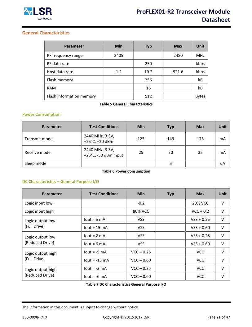
General Characteristics
Parameter Min Typ Max Unit
RF frequency range 2405 2480 MHz
RF data rate 250 kbps
Host data rate 1.2 19.2 921.6 kbps
Flash memory 256 kB
RAM 16 kB
Flash information memory 512 Bytes
Table 5 General Characteristics
Power Consumption
Parameter Test Conditions Min Typ Max Unit
Transmit mode 2440 MHz, 3.3V, +25°C, +20 dBm
125 149 175 mA
Receive mode 2440 MHz, 3.3V, +25°C, -50 dBm input
25 30 35 mA
Sleep mode 3 uA
Table 6 Power Consumption
DC Characteristics – General Purpose I/O
Parameter Test Conditions Min Typ Max Unit
Logic input low -0.2 20% VCC V
Logic input high 80% VCC VCC + 0.2 V
Logic output low (Full Drive)
Iout = 5 mA VSS VSS + 0.25 V
Iout = 15 mA VSS VSS + 0.60 V
Logic output low (Reduced Drive)
Iout = 2 mA VSS VSS + 0.25 V
Iout = 6 mA VSS VSS + 0.60 V
Logic output high (Full Drive)
Iout = -5 mA VCC – 0.25 VCC V
Iout = -15 mA VCC – 0.60 VCC V
Logic output high (Reduced Drive)
Iout = -2 mA VCC – 0.25 VCC V
Iout = -6 mA VCC – 0.60 VCC V
Table 7 DC Characteristics General Purpose I/O

ProFLEX01-R2 Transceiver Module
Datasheet
The information in this document is subject to change without notice. 330-0098-R4.0 Copyright © 2012-2017 LSR Page 22 of 47
RF Characteristics
Transmitter Characteristics (TA =25°C, VCC=3.3 V, fc =2440 MHz)
Parameter Test Conditions Min Typ Max Unit
Nominal output power 100mW 18 20 21 dBm
Programmable output power range
7 21 dB
Error vector magnitude 12 35 %
Table 8 Transmitter RF Characteristics
LSR Host RF Power Value
CC2520 TXPOWER Register Value
Typical RF Output Power
Typical Current Consumption
0
0x49 7 dBm 77 mA
1
2
3
4
5
6
7
8
9
10
0x79 12 dBm 92 mA 11
12
13 0x6C 16 dBm 105 mA
14
15 0xE0 18 dBm 122 mA
16
17
0xF9 20 dBm 149 mA 18
19
Table 9 RF Power Settings with LSR Host Software

ProFLEX01-R2 Transceiver Module
Datasheet
The information in this document is subject to change without notice. 330-0098-R4.0 Copyright © 2012-2017 LSR Page 23 of 47
Table 10 and Table 11 below list the nominal RF Power Limits per channel that must be maintained to assure compliance with FCC or ETSI.
RF Channel Max LSR Host RF Power
Value CC2520 TXPOWER Register
Value RF Output Power
11 16 0xE0 18 dBm
12 16 0xE0 18 dBm
13 16 0xE0 18 dBm
14 19 0xF9 20 dBm
15 19 0xF9 20 dBm
16 19 0xF9 20 dBm
17 19 0xF9 20 dBm
18 19 0xF9 20 dBm
19 19 0xF9 20 dBm
20 19 0xF9 20 dBm
21 19 0xF9 20 dBm
22 19 0xF9 20 dBm
23 19 0xF9 20 dBm
24 19 0xF9 20 dBm
25 16 0xE0 18 dBm
26 Not used Not used Not used
Table 10 RF Transmit Output Power Limits for FCC Compliance (Internal or External Antenna)
RF Channel
Max LSR Host RF Power Value
CC2520 TXPOWER Register Value
RF Output Power
11 Not used Not used Not used
12 9 0x49 7 dBm
13 9 0x49 7 dBm
14 9 0x49 7 dBm
15 9 0x49 7 dBm
16 9 0x49 7 dBm
17 9 0x49 7 dBm
18 9 0x49 7 dBm
19 9 0x49 7 dBm
20 9 0x49 7 dBm
21 9 0x49 7 dBm
22 9 0x49 7 dBm
23 9 0x49 7 dBm
24 9 0x49 7 dBm
25 9 0x49 7 dBm
26 9 0x49 7 dBm
Table 11 RF Transmit Output Power Limits for ETSI Compliance (Internal or External Antenna)

ProFLEX01-R2 Transceiver Module
Datasheet
The information in this document is subject to change without notice. 330-0098-R4.0 Copyright © 2012-2017 LSR Page 24 of 47
Receiver Characteristics (TA =25°C, VCC=3.3 V, fc =2440 MHz)
Parameter Test Conditions Min Typ Max Unit
Receiver sensitivity (1% PER)
HGM -95 -98 -99 dBm
Saturation (maximum input level) (1% PER)
HGM -13 dBm
Interference rejection
Desired signal at -82 dBm, 802.15.4 interferer
±5 MHz 51 dB
±10 MHz 56 dB
±20 MHz 57 dB
Table 12 Receiver RF Characteristics
For additional details regarding the electrical specifications, see the MSP430F5437A, CC2520, and CC2591 datasheets on the TI website.
ProFLEX01-R2 Transceiver Module
Datasheet
The information in this document is subject to change without notice. 330-0098-R4.0 Copyright © 2012-2017 LSR Page 25 of 47
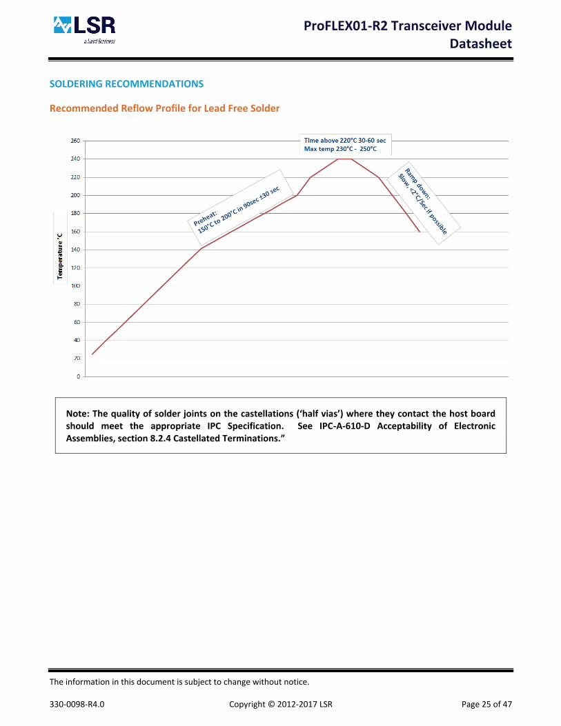
SOLDERING RECOMMENDATIONS
Recommended Reflow Profile for Lead Free Solder
Note: The quality of solder joints on the castellations (‘half vias’) where they contact the host board should meet the appropriate IPC Specification. See IPC-A-610-D Acceptability of Electronic Assemblies, section 8.2.4 Castellated Terminations.”

ProFLEX01-R2 Transceiver Module
Datasheet
The information in this document is subject to change without notice. 330-0098-R4.0 Copyright © 2012-2017 LSR Page 26 of 47
CLEANING
In general, cleaning the populated modules is strongly discouraged. Residuals under the module cannot be easily removed with any cleaning process.
• Cleaning with water can lead to capillary effects where water is absorbed into the gap between the host board and the module. The combination of soldering flux residuals and encapsulated water could lead to short circuits between neighboring pads. Water could also damage any stickers or labels.
• Cleaning with alcohol or a similar organic solvent will likely flood soldering flux residuals into the RF shield, which is not accessible for post-washing inspection. The solvent could also damage any stickers or labels.
• Ultrasonic cleaning could damage the module permanently.
OPTICAL INSPECTION
After soldering the Module to the host board, consider optical inspection to check the following:
• Proper alignment and centering of the module over the pads.
• Proper solder joints on all pads.
• Excessive solder or contacts to neighboring pads, or vias.
REWORK
The module can be unsoldered from the host board if the Moisture Sensitivity Level (MSL) requirements are met as described in this datasheet.
Never attempt a rework on the module itself, e.g. replacing individual components. Such actions will terminate warranty coverage.
SHIPPING, HANDLING, AND STORAGE
Shipping
Bulk orders of the ProFLEX01-R2 modules are delivered in trays of 25.
Handling
The ProFLEX01-R2 modules contain a highly sensitive electronic circuitry. Handling without proper ESD protection may destroy or damage the module permanently.
Moisture Sensitivity Level (MSL)
Per J-STD-020, devices rated as MSL 4 and not stored in a sealed bag with desiccant pack should be baked prior to use.
Devices are packaged in a Moisture Barrier Bag with a desiccant pack and Humidity Indicator Card (HIC). Devices that will be subjected to reflow should reference the HIC and J-STD-033 to determine if baking is required.
If baking is required, refer to J-STD-033 for bake procedure.
Storage
Per J-STD-033, the shelf life of devices in a Moisture Barrier Bag is 12 months at <40ºC and <90% room humidity (RH).
Do not store in salty air or in an environment with a high concentration of corrosive gas, such as Cl2, H2S, NH3, SO2, or NOX.
Do not store in direct sunlight.
The product should not be subject to excessive mechanical shock.

ProFLEX01-R2 Transceiver Module
Datasheet
The information in this document is subject to change without notice. 330-0098-R4.0 Copyright © 2012-2017 LSR Page 27 of 47
Repeating Reflow Soldering
Only a single reflow soldering process is encouraged for host boards.
ProFLEX01-R2 Transceiver Module
Datasheet
The information in this document is subject to change without notice. 330-0098-R4.0 Copyright © 2012-2017 LSR Page 28 of 47
AGENCY STATEMENTS
Agency Certifications
FCC ID: TFB-PROFLEX1
IC ID: 5969A-PROFLEX1
CE: Compliant to standards EN 60950-1, EN 300 328, and EN 301 489
Federal Communication Commission Interference Statement
This equipment has been tested and found to comply with the limits for a Class B digital device, pursuant to Part 15 of the FCC Rules. These limits are designed to provide reasonable protection against harmful interference in a residential installation. This equipment generates uses and can radiate radio frequency energy and, if not installed and used in accordance with the instructions, may cause harmful interference to radio communications. However, there is no guarantee that interference will not occur in a particular installation. If this equipment does cause harmful interference to radio or television reception, which can be determined by turning the equipment off and on, the user is encouraged to try to correct the interference by one of the following measures:
• Reorient or relocate the receiving antenna.
• Increase the separation between the equipment and receiver.
• Connect the equipment into an outlet on a circuit different from that to which the receiver is connected.
• Consult the dealer or an experienced radio/TV technician for help.
This device complies with Part 15 of the FCC Rules. Operation is subject to the following two conditions: (1) This device may not cause harmful interference, and (2) this device must accept any interference received, including interference that may cause undesired operation.
FCC CAUTION: Any changes or modifications not expressly approved by the party responsible for compliance could void the user's authority to operate this equipment.

ProFLEX01-R2 Transceiver Module
Datasheet
The information in this document is subject to change without notice. 330-0098-R4.0 Copyright © 2012-2017 LSR Page 29 of 47
Industry Canada Statements
Operation is subject to the following two conditions: (1) this device may not cause interference, and (2) this device must accept any interference, including interference that may cause undesired operation of the device.
To reduce potential radio interference to other users, the antenna type and its gain should be so chosen that the equivalent isotropically radiated power (e.i.r.p.) is not more than that permitted for successful communication.
This device has been designed to operate with the antennas listed below, and having a maximum gain of 2.0 dB. Antennas not included in this list or having a gain greater than 2.0 dB are strictly prohibited for use with this device. The required antenna impedance is 50 ohms.
• LSR 001-0001 2.4 GHz Dipole Antenna with Reverse Polarity SMA Connector and LSR 080-0001 U.FL to Reverse Polarity SMA Cable.
• Nearson S131CL-6-PX-2450S
• Embedded PCB trace antenna
ProFLEX01-R2 Transceiver Module
Datasheet
The information in this document is subject to change without notice. 330-0098-R4.0 Copyright © 2012-2017 LSR Page 30 of 47
OEM Responsibilities to comply with FCC and Industry Canada Regulations
The ProFLEX01-R2 Module has been certified for integration into products only by OEM integrators under the following conditions:
This device is granted for use in Mobile only configurations in which the antennas used for this transmitter must be installed to provide a separation distance of at least 20cm from all person and not be co-located with any other transmitters except in accordance with FCC and Industry Canada multi-transmitter product procedures.
As long as the two conditions above are met, further transmitter testing will not be required. However, the OEM integrator is still responsible for testing their end-product for any additional compliance requirements required with this module installed (for example, digital device emissions, PC peripheral requirements, etc.).
IMPORTANT NOTE: In the event that these conditions cannot be met (for certain configurations or co-location with another transmitter), then the FCC and Industry Canada authorizations are no longer considered valid and the FCC ID and IC Certification Number cannot be used on the final product. In these circumstances, the OEM integrator will be responsible for re-evaluating the end product (including the transmitter) and obtaining a separate FCC and Industry Canada authorization.
ProFLEX01-R2 Transceiver Module
Datasheet
The information in this document is subject to change without notice. 330-0098-R4.0 Copyright © 2012-2017 LSR Page 31 of 47
End Product Labelling
The ProFLEX01-R2 Module is labeled with its own FCC ID and IC Certification Number. If the FCC ID and IC Certification Number are not visible when the module is installed inside another device, then the outside of the device into which the module is installed must also display a label referring to the enclosed module. In that case, the final end product must be labeled in a visible area with the following:
“Contains Transmitter Module FCC ID: TFB-PROFLEX1”
“Contains Transmitter Module IC: 5969A-PROFLEX1”
or
“Contains FCC ID: TFB-PROFLEX1”
“Contains IC: 5969A-PROFLEX1”
The OEM of the ProFLEX01-R2 Module must only use the approved antenna(s) listed above, which have been certified with this module.
The OEM integrator has to be aware not to provide information to the end user regarding how to install or remove this RF module or change RF related parameters in the user manual of the end product.
The user manual for the end product must include the following information in a prominent location:
This device is granted for use in Mobile only configurations in which the antennas used for this transmitter must be installed to provide a separation distance of at least 20cm from all person and not be co-located with any other transmitters except in accordance with FCC and Industry Canada multi-transmitter product procedures.
ProFLEX01-R2 Transceiver Module
Datasheet
The information in this document is subject to change without notice. 330-0098-R4.0 Copyright © 2012-2017 LSR Page 32 of 47
EUROPE
CE Notice
This device has been tested and certified for use in the European Union. See the Declaration of Conformity (DoC) for specifics.
If this device is used in a product, the OEM has responsibility to verify compliance of the final product to the EU standards. A Declaration of Conformity must be issued and kept on file as described in the Radio and Telecommunications Terminal Equipment (R&TTE) Directive. The ‘CE’ mark must be placed on the OEM product per the labeling requirements of the Directive.
Declaration of Conformity (DoC)
This DoC can be downloaded from the LSR Wiki.

ProFLEX01-R2 Transceiver Module
Datasheet
The information in this document is subject to change without notice. 330-0098-R4.0 Copyright © 2012-2017 LSR Page 33 of 47
ANTENNA INFORMATION
Dipole Antenna 001-0001
See antenna datasheet.
F Antenna
Flat 2.405 GHz
Figure 14 Flat 2.405 GHz
-30
-25
-20
-15
-10
-5
0
5
30
210
60
240
90
270
120
300
150
330
180 0
____Vertical Polarization Gain (dBi) min: -40.4 max: -11.3 avg: -17.4
------- Horizontal Polarization Gain (dBi) min: -24.3 max: +2.4 avg: -1.6
ProFLEX01-R2 Transceiver Module
Datasheet
The information in this document is subject to change without notice. 330-0098-R4.0 Copyright © 2012-2017 LSR Page 34 of 47
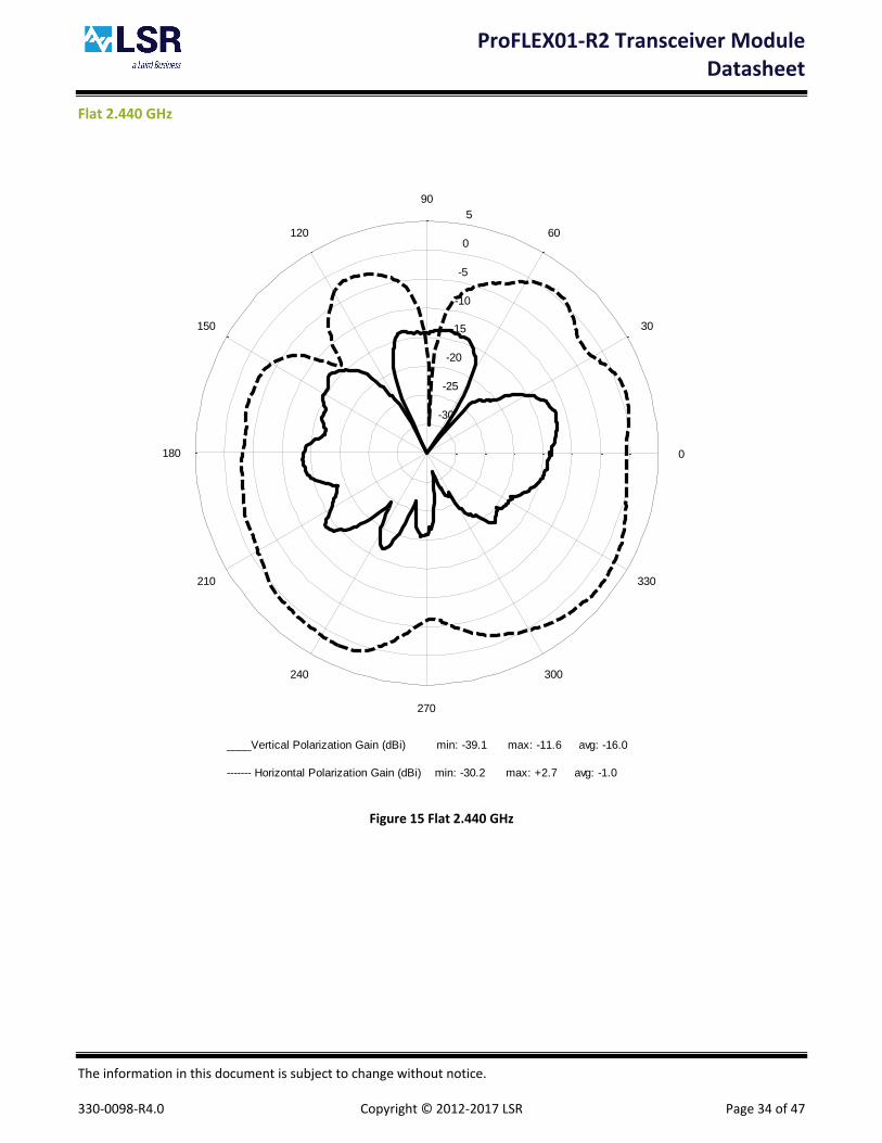
Flat 2.440 GHz
Figure 15 Flat 2.440 GHz
-30
-25
-20
-15
-10
-5
0
5
30
210
60
240
90
270
120
300
150
330
180 0
____Vertical Polarization Gain (dBi) min: -39.1 max: -11.6 avg: -16.0
------- Horizontal Polarization Gain (dBi) min: -30.2 max: +2.7 avg: -1.0

ProFLEX01-R2 Transceiver Module
Datasheet
The information in this document is subject to change without notice. 330-0098-R4.0 Copyright © 2012-2017 LSR Page 35 of 47
Flat 2.480 GHz
Figure 16 Flat 2.480 GHz
-30
-25
-20
-15
-10
-5
0
5
30
210
60
240
90
270
120
300
150
330
180 0
____Vertical Polarization Gain (dBi) min: -41.2 max: -10.7 avg: -15.6
------- Horizontal Polarization Gain (dBi) min: -19.1 max: +2.5 avg: -0.4

ProFLEX01-R2 Transceiver Module
Datasheet
The information in this document is subject to change without notice. 330-0098-R4.0 Copyright © 2012-2017 LSR Page 36 of 47
Side 2.405 GHz
Figure 17 Side 2.405 GHz
-30
-25
-20
-15
-10
-5
0
5
30
210
60
240
90
270
120
300
150
330
180 0
____Vertical Polarization Gain (dBi) min: -20.2 max: -2.3 avg: -6.2
------- Horizontal Polarization Gain (dBi) min: -33.4 max: -4.4 avg: -9.0

ProFLEX01-R2 Transceiver Module
Datasheet
The information in this document is subject to change without notice. 330-0098-R4.0 Copyright © 2012-2017 LSR Page 37 of 47
Side 2.440 GHz
Figure 18 Side 2.440 GHz
-30
-25
-20
-15
-10
-5
0
5
30
210
60
240
90
270
120
300
150
330
180 0
____Vertical Polarization Gain (dBi) min: -14.6 max: -0.6 avg: -6.7
------- Horizontal Polarization Gain (dBi) min: -28.3 max: -6.2 avg: -9.9

ProFLEX01-R2 Transceiver Module
Datasheet
The information in this document is subject to change without notice. 330-0098-R4.0 Copyright © 2012-2017 LSR Page 38 of 47
Side 2.480 GHz
Figure 19 Side 2.480 GHz
-30
-25
-20
-15
-10
-5
0
5
30
210
60
240
90
270
120
300
150
330
180 0
____Vertical Polarization Gain (dBi) min: -25.3 max: -1.2 avg: -6.3
------- Horizontal Polarization Gain (dBi) min: -19.5 max: -6.1 avg: -10.2

ProFLEX01-R2 Transceiver Module
Datasheet
The information in this document is subject to change without notice. 330-0098-R4.0 Copyright © 2012-2017 LSR Page 39 of 47
Vertical 2.405 GHz
Figure 20 Vertical 2.405 GHz
-30
-25
-20
-15
-10
-5
0
5
30
210
60
240
90
270
120
300
150
330
180 0
____Vertical Polarization Gain (dBi) min: -9.4 max: +0.6 avg: -3.1
------- Horizontal Polarization Gain (dBi) min: -13.1 max: +1.3 avg: -3.5

ProFLEX01-R2 Transceiver Module
Datasheet
The information in this document is subject to change without notice. 330-0098-R4.0 Copyright © 2012-2017 LSR Page 40 of 47
Vertical 2.440 GHz
Figure 21 Vertical 2.440 GHz
-30
-25
-20
-15
-10
-5
0
5
30
210
60
240
90
270
120
300
150
330
180 0
____Vertical Polarization Gain (dBi) min: -8.7 max: +0.8 avg: -3.1
------- Horizontal Polarization Gain (dBi) min: -15.6 max: +1.4 avg: -3.0

ProFLEX01-R2 Transceiver Module
Datasheet
The information in this document is subject to change without notice. 330-0098-R4.0 Copyright © 2012-2017 LSR Page 41 of 47
Vertical 2.480 GHz
Figure 22 Vertical 2.480 GHz
-30
-25
-20
-15
-10
-5
0
5
30
210
60
240
90
270
120
300
150
330
180 0
____Vertical Polarization Gain (dBi) min: -7.8 max: +1.5 avg: -2.3
------- Horizontal Polarization Gain (dBi) min: -15.5 max: +2.1 avg: -2.3
ProFLEX01-R2 Transceiver Module
Datasheet
The information in this document is subject to change without notice. 330-0098-R4.0 Copyright © 2012-2017 LSR Page 42 of 47
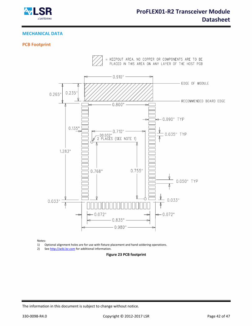
MECHANICAL DATA
PCB Footprint
Notes: 1) Optional alignment holes are for use with fixture placement and hand soldering operations. 2) See http://wiki.lsr.com for additional information.
Figure 23 PCB footprint

ProFLEX01-R2 Transceiver Module
Datasheet
The information in this document is subject to change without notice. 330-0098-R4.0 Copyright © 2012-2017 LSR Page 43 of 47
General Module Dimensions
Figure 24 Basic dimensions
ProFLEX01-R2 Transceiver Module
Datasheet
The information in this document is subject to change without notice. 330-0098-R4.0 Copyright © 2012-2017 LSR Page 44 of 47
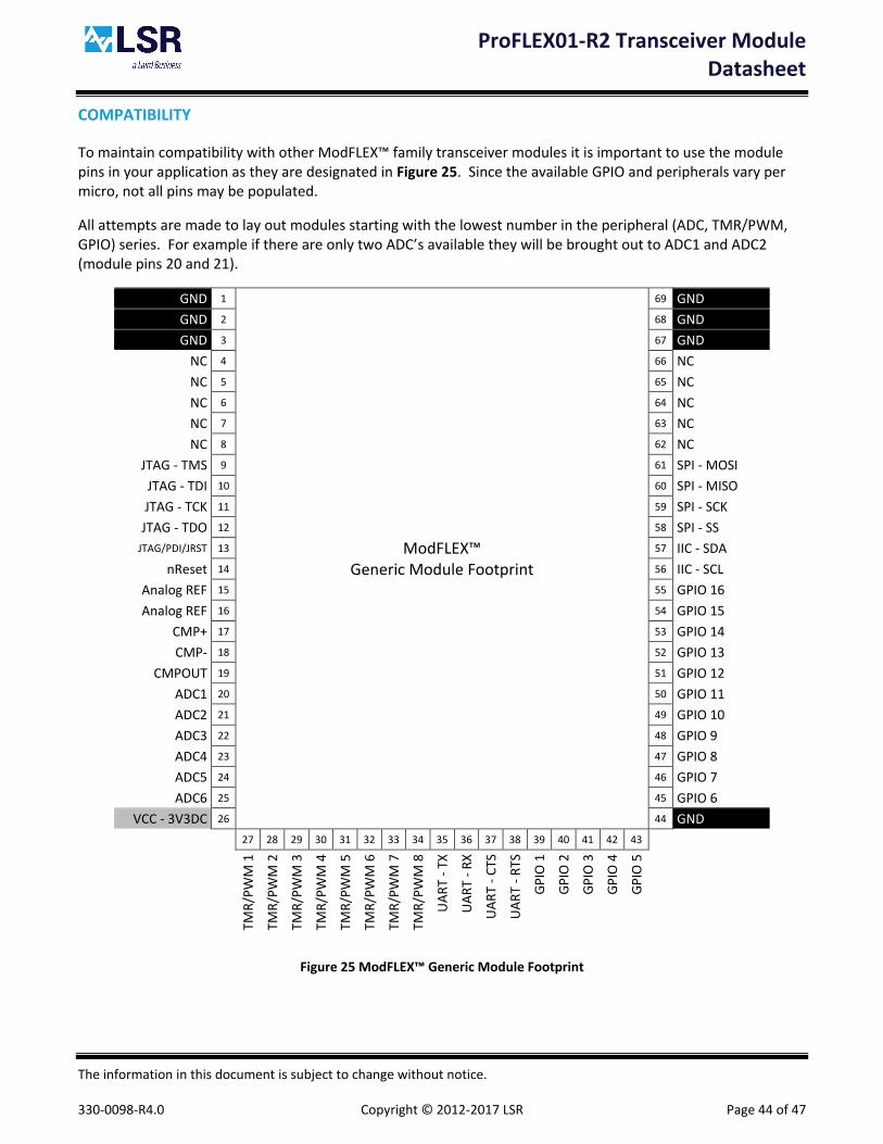
COMPATIBILITY
To maintain compatibility with other ModFLEX™ family transceiver modules it is important to use the module pins in your application as they are designated in Figure 25. Since the available GPIO and peripherals vary per micro, not all pins may be populated.
All attempts are made to lay out modules starting with the lowest number in the peripheral (ADC, TMR/PWM, GPIO) series. For example if there are only two ADC’s available they will be brought out to ADC1 and ADC2 (module pins 20 and 21).
GND 1
ModFLEX™ Generic Module Footprint
69 GND
GND 2 68 GND
GND 3 67 GND
NC 4 66 NC
NC 5 65 NC
NC 6 64 NC
NC 7 63 NC
NC 8 62 NC
JTAG - TMS 9 61 SPI - MOSI
JTAG - TDI 10 60 SPI - MISO
JTAG - TCK 11 59 SPI - SCK
JTAG - TDO 12 58 SPI - SS
JTAG/PDI/JRST 13 57 IIC - SDA
nReset 14 56 IIC - SCL
Analog REF 15 55 GPIO 16
Analog REF 16 54 GPIO 15
CMP+ 17 53 GPIO 14
CMP- 18 52 GPIO 13
CMPOUT 19 51 GPIO 12
ADC1 20 50 GPIO 11
ADC2 21 49 GPIO 10
ADC3 22 48 GPIO 9
ADC4 23 47 GPIO 8
ADC5 24 46 GPIO 7
ADC6 25 45 GPIO 6
VCC - 3V3DC 26 44 GND
27 28 29 30 31 32 33 34 35 36 37 38 39 40 41 42 43
TMR
/PW
M 1
TMR
/PW
M 2
TMR
/PW
M 3
TMR
/PW
M 4
TMR
/PW
M 5
TMR
/PW
M 6
TMR
/PW
M 7
TMR
/PW
M 8
UA
RT
- TX
UA
RT
- R
X
UA
RT
- C
TS
UA
RT
- R
TS
GP
IO 1
GP
IO 2
GP
IO 3
GP
IO 4
GP
IO 5
Figure 25 ModFLEX™ Generic Module Footprint

ProFLEX01-R2 Transceiver Module
Datasheet
The information in this document is subject to change without notice. 330-0098-R4.0 Copyright © 2012-2017 LSR Page 45 of 47
MODULE REVISION HISTORY
Rev 1
• Initial production release.
LS RESEARCH
MAC ID: 00:25:CA:02:XX:XX:XX:XX
00:25:CA:02:XX:XX:XX = MAC ID
2D Barcode Format is Data Matrix Standard
XX:XX:XX:XX = unique portion of MAC ID that
changes for each module
Wireless Product Development
M/N: ProFLEX01-R2 P/N: 450-0075
RE
V 1 2D
Bar
Code
FCC ID: TFB-PROFLEX1
IC: 5969A-PROFLEX1
RoHS
Part Number: 450-0075
F Antenna Module
Rev 2
• Module Firmware Updated.
LS RESEARCH
MAC ID: 00:25:CA:02:XX:XX:XX:XX
Wireless Product Development
M/N: ProFLEX01-R2 P/N: 450-0075
RE
V 2 2D
Bar
Code
FCC ID: TFB-PROFLEX1
IC: 5969A-PROFLEX1
RoHS
Part Number: 450-0075
F Antenna Module
LS RESEARCH
MAC ID: 00:25:CA:02:XX:XX:XX:XX
00:25:CA:02:XX:XX:XX = MAC ID
2D Barcode Format is Data Matrix Standard
XX:XX:XX:XX = unique portion of MAC ID that
changes for each module
Wireless Product Development
M/N: ProFLEX01-R2 P/N: 450-0076
RE
V 1 2D
Bar
Code
FCC ID: TFB-PROFLEX1
IC: 5969A-PROFLEX1
RoHS
Part Number: 450-0076
U.FL Module
LS RESEARCH
MAC ID: 00:25:CA:02:XX:XX:XX:XX
Wireless Product Development
M/N: ProFLEX01-R2 P/N: 450-0076
RE
V 2 2D
Bar
Code
FCC ID: TFB-PROFLEX1
IC: 5969A-PROFLEX1
RoHS
Part Number: 450-0076
U.FL Module
ProFLEX01-R2 Transceiver Module
Datasheet
The information in this document is subject to change without notice. 330-0098-R4.0 Copyright © 2012-2017 LSR Page 46 of 47
Rev 3
• Module Firmware Updated.
LS RESEARCH
MAC ID: 00:25:CA:02:XX:XX:XX:XX
Wireless P roduct Development
M/N: ProFLEX 01-R2 P/N: 450-0075
RE
V 3 2D
B ar
C ode
FCC ID: TFB-PROFLEX1
IC: 5969A-PROFLEX1
RoHS
Part Num ber : 450-0075
F Antenna M odul e
LS RESEARCH
MAC ID: 00:25:CA:02:XX:XX:XX:XX
Wireless P roduct Development
M/N: ProFLEX 01-R2 P/N: 450-0076
RE
V 3 2D
B ar
C ode
FCC ID: TFB-PROFLEX1
IC: 5969A-PROFLEX1
RoHS
Part Num ber : 450-0076
U.FL Module
Rev 4
• Module Firmware Updated.
Part Number: 450-0075 F-Antenna Module
ProFLEX01-R2 Transceiver Module
Datasheet
The information in this document is subject to change without notice. 330-0098-R4.0 Copyright © 2012-2017 LSR Page 47 of 47
CONTACTING LSR
Headquarters LSR W66 N220 Commerce Court Cedarburg, WI 53012-2636 USA Tel: 1(262) 375-4400 Fax: 1(262) 375-4248
Website www.lsr.com
Sales Contact [email protected]
The information in this document is provided in connection with LS Research (hereafter referred to as “LSR”) products. No license, express or implied, by estoppel or otherwise, to any intellectual property right is granted by this document or in connection with the sale of LSR products. EXCEPT AS SET FORTH IN LSR’S TERMS AND CONDITIONS OF SALE LOCATED ON LSR’S WEB SITE, LSR ASSUMES NO LIABILITY WHATSOEVER AND DISCLAIMS ANY EXPRESS, IMPLIED OR STATUTORY WARRANTY RELATING TO ITS PRODUCTS INCLUDING, BUT NOT LIMITED TO, THE IMPLIED WARRANTY OF MERCHANTABILITY, FITNESS FOR A PARTICULAR PURPOSE, OR NON-INFRINGEMENT. IN NO EVENT SHALL LSR BE LIABLE FOR ANY DIRECT, INDIRECT, CONSEQUENTIAL, PUNITIVE, SPECIAL OR INCIDENTAL DAMAGES (INCLUDING, WITHOUT LIMITATION, DAMAGES FOR LOSS OF PROFITS, BUSINESS INTERRUPTION, OR LOSS OF INFORMATION) ARISING OUT OF THE USE OR INABILITY TO USE THIS DOCUMENT, EVEN IF LSR HAS BEEN ADVISED OF THE POSSIBILITY OF SUCH DAMAGES. LSR makes no representations or warranties with respect to the accuracy or completeness of the contents of this document and reserves the right to make changes to specifications and product descriptions at any time without notice. LSR does not make any commitment to update the information contained herein. Unless specifically provided otherwise, LSR products are not suitable for, and shall not be used in, automotive applications. LSR’s products are not intended, authorized, or warranted for use as components in applications intended to support or sustain life.


![RF Module Design - [Chapter 4] Transceiver Architecture](https://img.dokumen.tips/doc/110x75/55ca514abb61eb59138b45c0/rf-module-design-chapter-4-transceiver-architecture.jpg)

