Embed Size (px)
Citation preview
Prof. Dr. F. Dildey Dipl.-Ing. J.-C. Böhmke Fakultät Life Sciences
Praktikum Elektronik 2 Versuch 1
Operationsverstärker
- 1 von 6 - Version 1.0 Stand WS 2012 / 2013
1. Lernziel Der Einsatz und Umgang mit dem Operationsverstärker (OP) soll anhand von einfachen Standardschaltungen verstanden werden. Der Umgang mit Datenblättern und die Dimensionierung der Beschaltung sollen geübt werden.
2. Allgemeines
3. Vorbereitung
3.1 Begriffe
Zur Vorbereitung dieses Versuchs müssen Sie sich über folgende Begriffe in Kenntnis setzen:
- Verstärkung des OP - Verstärkung der Schaltung (A oder V) - Offsetspannung - Transitfrequenz - Bandbreite - Invertierender und Nicht-invertierender Verstärker - Addierer (Summierverstärker) - Bandpass
3.2 Aufgaben zur Vorbereitung des Praktikums
Die Schaltungsentwürfe mit den Angaben aller Widerstandswerte und die Rechenergebnisse sind bei Praktikumsbeginn vorzulegen. Benutzen Sie hierfür die Lösungsbögen im Anhang. Zu allen Aufgaben ist ein vollständiges Schaltbild zu zeichnen. Dabei sind die Anschlüsse entsprechend den Datenblättern zu nummerieren. 3.2.1 Stellen Sie sich vor, Sie legen eine kleine Wechselspannung (Sinus, 20 mV Amplitude, 100 Hz) direkt
an die Eingänge des OP. Die Spannungsversorgung soll ±5 V betragen.
Skizzieren Sie den vermuteten Verlauf der Ausgangsspannung und begründen Sie ihre Überlegungen.
Spannungsangaben ohne Zusatz beziehen sich auf den Effektivwert,
eine Amplitudenangabe der Spannung bezieht sich auf den Scheitelwert.
Prof. Dr. F. Dildey Dipl.-Ing. J.-C. Böhmke Fakultät Life Sciences
Praktikum Elektronik 2 Versuch 1
Operationsverstärker
- 2 von 6 - Version 1.0 Stand WS 2012 / 2013
3.2.2 Dimensionieren Sie die Widerstände für einen nicht-invertierenden Verstärker (OP Typ LF356, s.
Anhang) mit einer Spannungsverstärkung von A = 23. Wählen Sie R1 = 10 kΩ (Widerstand gegen Masse). Zeichnen Sie das vollständige Schaltbild.
3.2.3 Wie groß ist die Ausgangsspannung, wenn Sie den Eingang der Schaltung aus 3.2.2. auf Masse
legen? Hinweis: Für die Beantwortung dieser Frage benötigen Sie Werte aus dem Datenblatt.
3.2.4. Dimensionieren Sie die Widerstände für einen invertierenden Verstärker
(OP Typ LF356, s. Anhang) mit einer Spannungsverstärkung von
A = - 3,3 sowie A = -10,0
Der Eingangswiderstand der Schaltung soll 10 kΩ betragen. Zeichnen Sie das vollständige Schaltbild.
3.2.5. Entwerfen Sie eine Stromquelle mit dem OP LF 356.
Dabei sollen
R = 1,0 kΩ , I = 1,0 mA und die Versorgungsspannung ± 5 V betragen.
- Wie groß wählen Sie die Eingangsgleichspannung Ue?
- Welche Spannungen liegen am RL, wenn dieser
1,0 kΩ – 1,5 kΩ – 2,2 kΩ groß ist?
- Wie groß kann der RL maximal werden, bis die Stromquelle an ihre Grenzen stößt?
3.2.6. Für den Eingang eines Analog-Digital-Wandlers benötigen Sie ein Signal mit folgenden Eigenschaften:
Ihnen stehen eine Wechselspannung mit 0,5 V Amplitude (Sinus,100 Hz) und eine Gleichspannung
von 1,5 V zur Verfügung. Entwerfen Sie einen Addierer (Summierverstärker) mit dem LF 356, der die entsprechende Signalwandlung durchführt.
Wählen Sie für den Gegenkopplungswiderstand R2 =10 kΩ.
Prof. Dr. F. Dildey Dipl.-Ing. J.-C. Böhmke Fakultät Life Sciences
Praktikum Elektronik 2 Versuch 1
Operationsverstärker
- 3 von 6 - Version 1.0 Stand WS 2012 / 2013
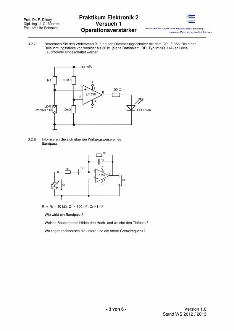
3.2.7 Berechnen Sie den Widerstand R1 für einen Dämmerungsschalter mit dem OP LF 356. Bei einer
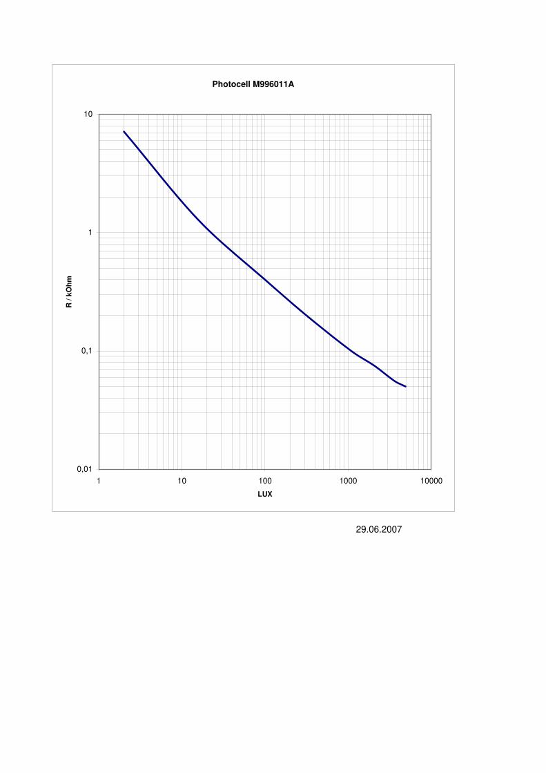
Beleuchtungsstärke von weniger als 30 lx (siehe Datenblatt LDR, Typ M996011A) soll eine Leuchtdiode eingeschaltet werden.
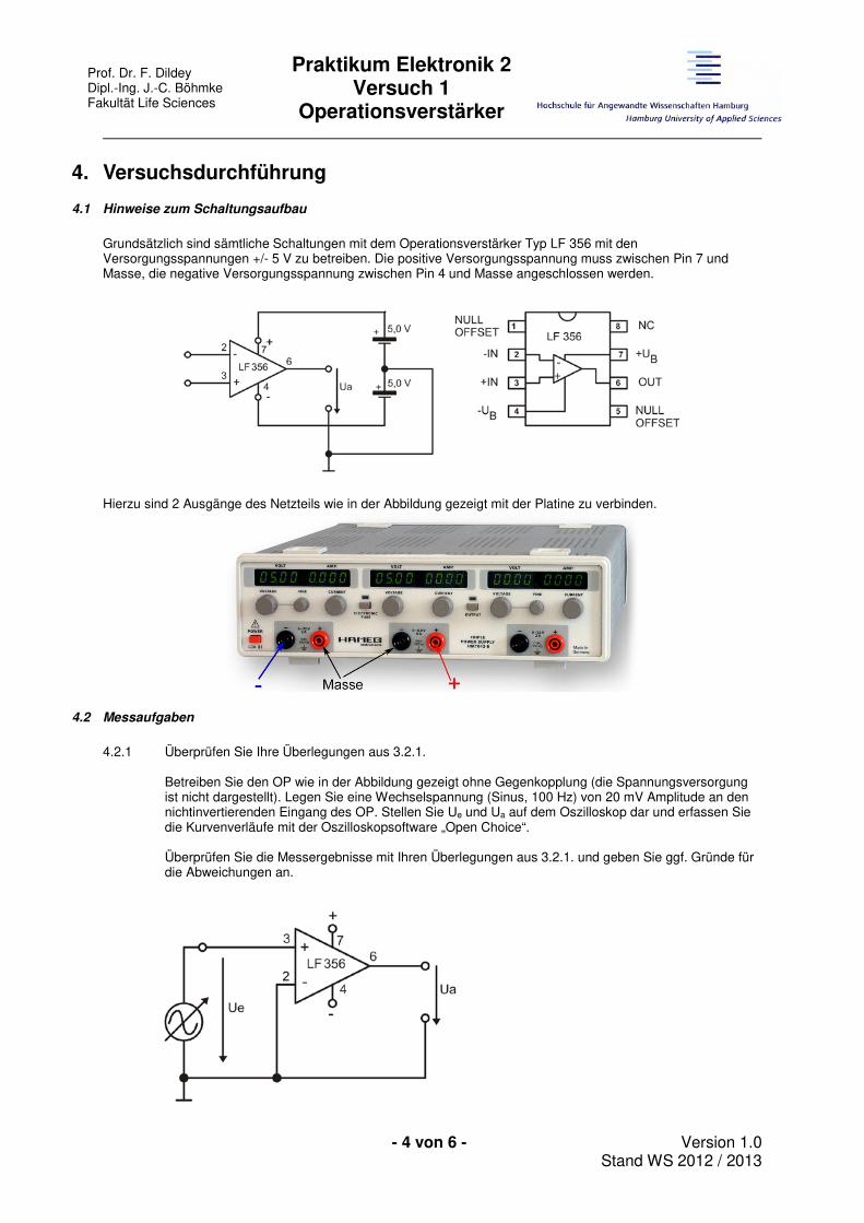
3.2.8 Informieren Sie sich über die Wirkungsweise eines
Bandpass.
R1 = R2 = 10 kΩ, C1 = 100 nF, C2 =1 nF
- Wie wirkt ein Bandpass?
- Welche Bauelemente bilden den Hoch- und welche den Tiefpass?
- Wo liegen rechnerisch die untere und die obere Grenzfrequenz?
Prof. Dr. F. Dildey Dipl.-Ing. J.-C. Böhmke Fakultät Life Sciences
Praktikum Elektronik 2 Versuch 1
Operationsverstärker
- 4 von 6 - Version 1.0 Stand WS 2012 / 2013
4. Versuchsdurchführung
4.1 Hinweise zum Schaltungsaufbau
Grundsätzlich sind sämtliche Schaltungen mit dem Operationsverstärker Typ LF 356 mit den Versorgungsspannungen +/- 5 V zu betreiben. Die positive Versorgungsspannung muss zwischen Pin 7 und Masse, die negative Versorgungsspannung zwischen Pin 4 und Masse angeschlossen werden.
Hierzu sind 2 Ausgänge des Netzteils wie in der Abbildung gezeigt mit der Platine zu verbinden.
4.2 Messaufgaben
4.2.1 Überprüfen Sie Ihre Überlegungen aus 3.2.1.
Betreiben Sie den OP wie in der Abbildung gezeigt ohne Gegenkopplung (die Spannungsversorgung ist nicht dargestellt). Legen Sie eine Wechselspannung (Sinus, 100 Hz) von 20 mV Amplitude an den nichtinvertierenden Eingang des OP. Stellen Sie Ue und Ua auf dem Oszilloskop dar und erfassen Sie die Kurvenverläufe mit der Oszilloskopsoftware „Open Choice“. Überprüfen Sie die Messergebnisse mit Ihren Überlegungen aus 3.2.1. und geben Sie ggf. Gründe für die Abweichungen an.

Prof. Dr. F. Dildey Dipl.-Ing. J.-C. Böhmke Fakultät Life Sciences
Praktikum Elektronik 2 Versuch 1
Operationsverstärker
- 5 von 6 - Version 1.0 Stand WS 2012 / 2013
4.2.2 Bauen Sie die Schaltung eines Nicht-invertierenden Verstärkers nach 3.2.2. auf. Steuern Sie die
Schaltung mit einem Sinussignal 100 mV, 100 Hz an.
- Messen Sie die Verstärkung der Stufe.
4.2.3 Legen Sie den Eingang auf Masse und messen sie die Ausgangsspannung Ua.
- Wie groß ist die Offsetspannung des OP?
4.2.4 Bauen Sie den invertierenden Verstärker nach 3.2.4 auf. Steuern Sie die Schaltung mit einem
Sinussignal 100 mV, 100 Hz an.
- Messen Sie die Verstärkungen der beiden Schaltungen.
- Messen Sie bei jeder Verstärkung die Grenzfrequenz. Welcher Zusammenhang besteht zwischen der Verstärkung und der Grenzfrequenz der Schaltung? Welcher Kennwert wird hierzu im Datenblatt genannt?
4.2.5 Bauen Sie eine Stromquelle mit dem OP LF 356 nach 3.2.5. auf und setzen Sie für RL nacheinander
1,0 kΩ, 1,5 kΩ und 2,2 kΩ ein.
- Messen Sie mit dem Multimeter den Spannungsabfall am RL und errechnen Sie daraus den Strom. Ist die Funktion einer Stromquelle gegeben?
4.2.6 Bauen Sie den Addierer nach 3.2.6. auf und überprüfen Sie, ob das Ausgangssignal den gewünschten
Verlauf aufweist. Erfassen Sie den Kurvenverlauf von Ua mit der Oszilloskopsoftware „Open Choice“.
4.2.7 Bauen Sie den Dämmerungschalter nach 3.2.7. auf und überprüfen Sie seine Funktion. Notieren Sie Ihre Beobachtungen.
4.2.8 Bauen Sie den Bandpass nach 3.2.8. auf.
- Nehmen Sie die Funktion Ua = f(f) auf bei:
0,1kHz, 1,0kHz, 2,0kHz, 10kHz, 100kHz, 150kHz, 200kHz
- Erstellen Sie mit Excel ein Diagramm A=f(f). Achten Sie auf eine sinnvolle Skalierung der Achsen.
- Wie groß ist die maximale Verstärkung?
- Ermitteln Sie aus dem Diagramm die untere und die obere Grenzfrequenz.
Wie groß ist die Bandbreite der Schaltung?
Prof. Dr. F. Dildey Dipl.-Ing. J.-C. Böhmke Fakultät Life Sciences
Praktikum Elektronik 2 Versuch 1
Operationsverstärker
- 6 von 6 - Version 1.0 Stand WS 2012 / 2013
5. Anhang
5.1 Geräteliste
1x Versuchsplatine mit Operationsverstärker Typ LF 356 1x Oszilloskop Tektronix Typ TDS 2002C 1x Dreifachnetzgerät HAMEG Typ HM 7042-5 1x Funktionsgenerator HAMEG Typ HM 8030-6 1x Einbaumultimeter HAMEG Typ HM 8012 2x Handmultimeter Fluke 83 oder 83V
5.2 Literaturhinweise
Tietze/Schenk Halbleiterschaltungstechnik Springer Verlag ISBN 3-540-42849-6 L.Palotas Elektronik für Ingenieure: Analoge und digitale integrierte Schaltungen Vieweg Verlag ISBN 978-3528039158
E. Hering K. Bressle J. Gutekunst Elektronik für Ingenieure Springer Verlag ISBN 3-540-41738-9 H.Hinsch Elektronik-Ein Werkzeug für Naturwissenschaftler Springer Verlag ISBN 978-3540613602
Folgende Geräteanleitungen finden Sie auf der Laborhomepage: Fluke Multimeter Typ 83, 83/V, 87/III, 179 Tektronix Oszilloskop TDS 2002C HAMEG Labornetzgerät HM7042-5 HAMEG Multimeter HM8012 HAMEG Funktionsgenerator HM 8030-6
5.3 Lösungsbögen und Datenblätter
Lösungsbögen und Datenblätter folgen auf den nächsten Seiten…
Prof. Dr. F. Dildey Dipl.-Ing. J.-C. Böhmke Fakultät Life Sciences
Praktikum Elektronik 2 Lösungsbögen zu
Versuch 1
- 1 von 5 - Version 1.0 Stand WS 2012 / 2013
1. Vorbereitung
zu 3.2.1. Verlauf von Ua bei offenem OP:
Begründung:
zu 3.2.2. Nichtinvertierender Verstärker, A = 23
Prof. Dr. F. Dildey Dipl.-Ing. J.-C. Böhmke Fakultät Life Sciences
Praktikum Elektronik 2 Lösungsbögen zu
Versuch 1
- 2 von 5 - Version 1.0 Stand WS 2012 / 2013
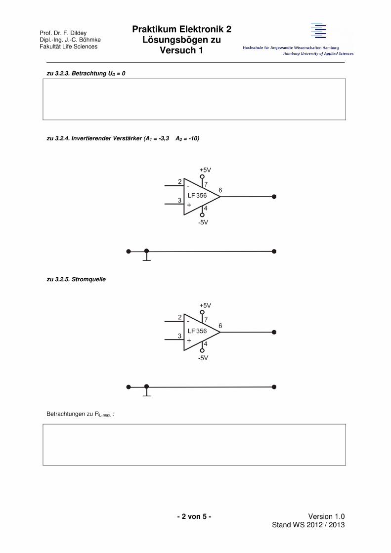
zu 3.2.3. Betrachtung UD = 0
zu 3.2.4. Invertierender Verstärker (A1 = -3,3 A2 = -10)
zu 3.2.5. Stromquelle
Betrachtungen zu RL,max. :
Prof. Dr. F. Dildey Dipl.-Ing. J.-C. Böhmke Fakultät Life Sciences
Praktikum Elektronik 2 Lösungsbögen zu
Versuch 1
- 3 von 5 - Version 1.0 Stand WS 2012 / 2013
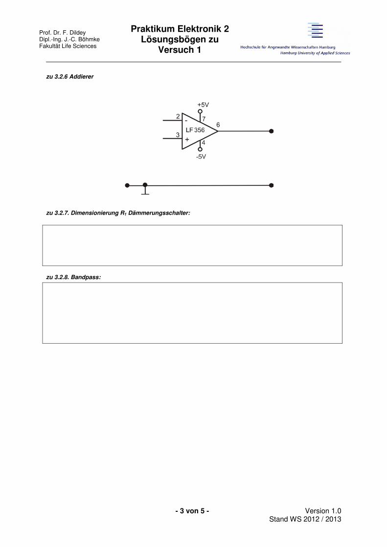
zu 3.2.6 Addierer
zu 3.2.7. Dimensionierung R1 Dämmerungsschalter:
zu 3.2.8. Bandpass:
Prof. Dr. F. Dildey Dipl.-Ing. J.-C. Böhmke Fakultät Life Sciences
Praktikum Elektronik 2 Lösungsbögen zu
Versuch 1
- 4 von 5 - Version 1.0 Stand WS 2012 / 2013
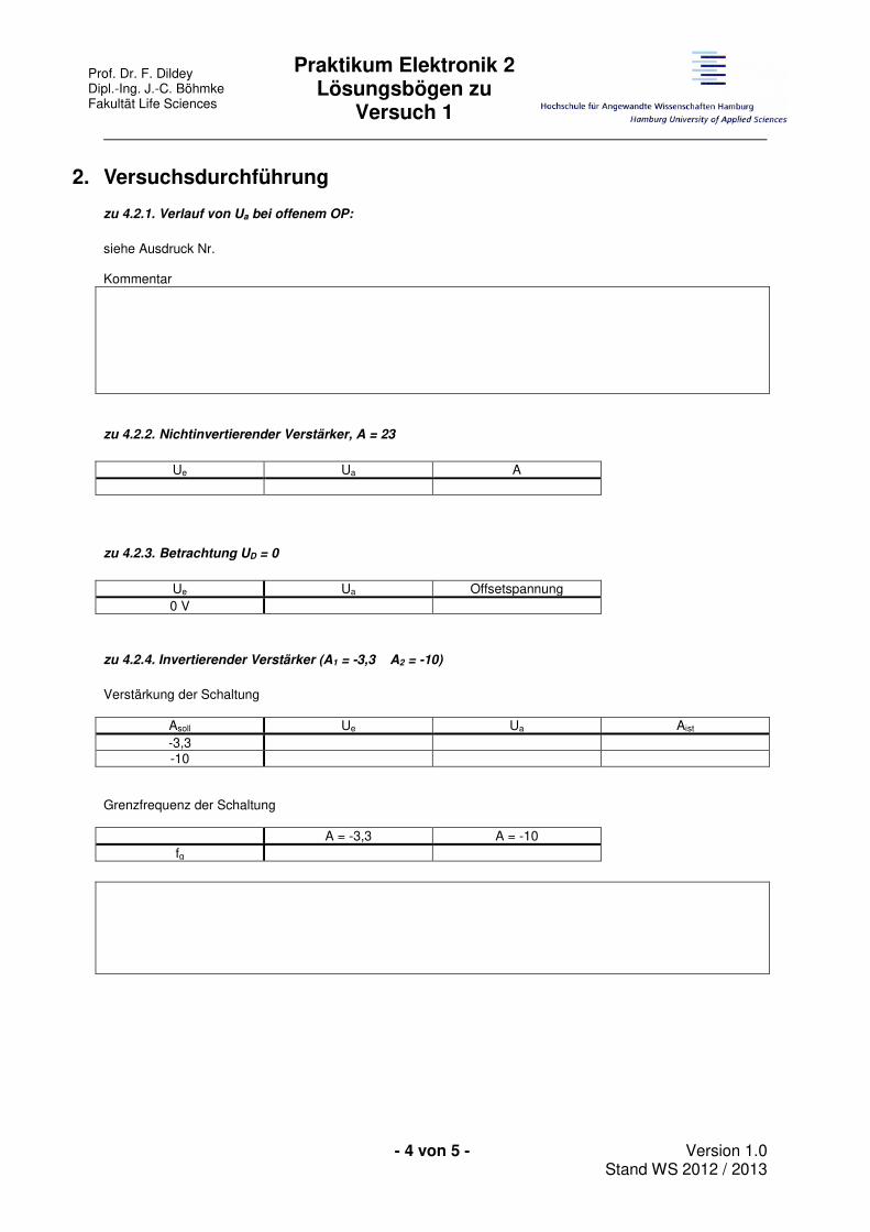
2. Versuchsdurchführung
zu 4.2.1. Verlauf von Ua bei offenem OP:
siehe Ausdruck Nr. Kommentar
zu 4.2.2. Nichtinvertierender Verstärker, A = 23
Ue Ua A
zu 4.2.3. Betrachtung UD = 0
Ue Ua Offsetspannung 0 V
zu 4.2.4. Invertierender Verstärker (A1 = -3,3 A2 = -10)
Verstärkung der Schaltung
Asoll Ue Ua Aist -3,3 -10
Grenzfrequenz der Schaltung
A = -3,3 A = -10 fg
Prof. Dr. F. Dildey Dipl.-Ing. J.-C. Böhmke Fakultät Life Sciences
Praktikum Elektronik 2 Lösungsbögen zu
Versuch 1
- 5 von 5 - Version 1.0 Stand WS 2012 / 2013
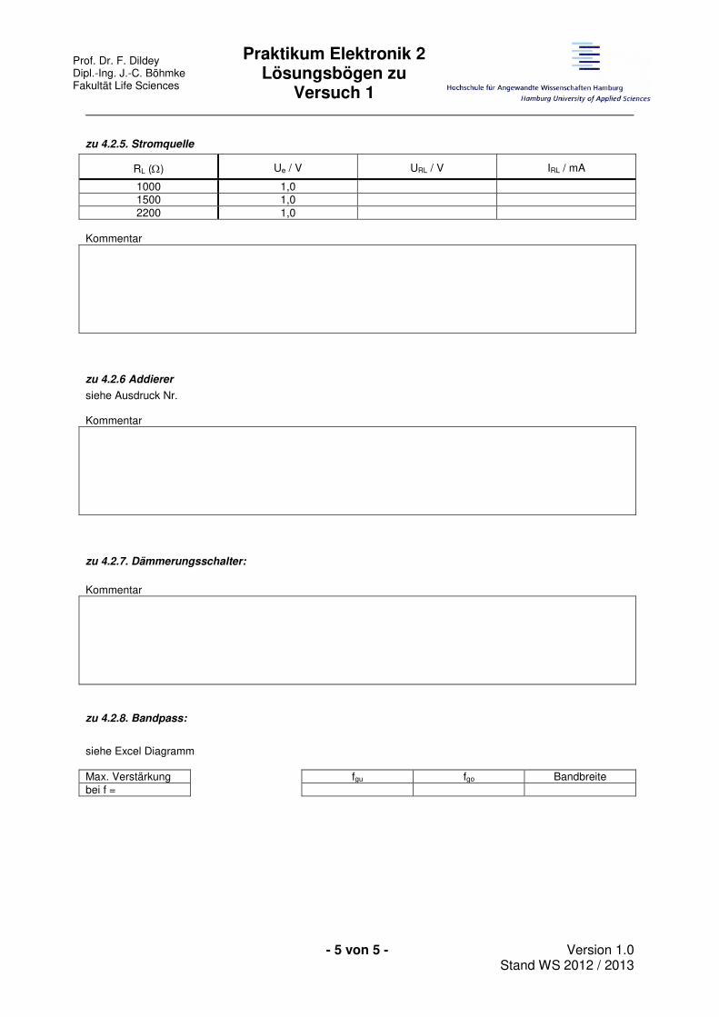
zu 4.2.5. Stromquelle
RL (Ω)
Ue / V
URL / V
IRL / mA
1000 1,0 1500 1,0 2200 1,0
Kommentar
zu 4.2.6 Addierer
siehe Ausdruck Nr. Kommentar
zu 4.2.7. Dämmerungsschalter:
Kommentar
zu 4.2.8. Bandpass:
siehe Excel Diagramm Max. Verstärkung fgu fgo Bandbreite bei f =

LF155/LF156/LF256/LF257/LF355/LF356/LF357
JFET Input Operational AmplifiersGeneral DescriptionThese are the first monolithic JFET input operational ampli-fiers to incorporate well matched, high voltage JFETs on thesame chip with standard bipolar transistors (BI-FET™ Tech-nology). These amplifiers feature low input bias and offsetcurrents/low offset voltage and offset voltage drift, coupledwith offset adjust which does not degrade drift orcommon-mode rejection. The devices are also designed forhigh slew rate, wide bandwidth, extremely fast settling time,low voltage and current noise and a low 1/f noise corner.
FeaturesAdvantages
n Replace expensive hybrid and module FET op amps
n Rugged JFETs allow blow-out free handling comparedwith MOSFET input devices
n Excellent for low noise applications using either high orlow source impedance — very low 1/f corner
n Offset adjust does not degrade drift or common-moderejection as in most monolithic amplifiers
n New output stage allows use of large capacitive loads(5,000 pF) without stability problems
n Internal compensation and large differential input voltagecapability
Applicationsn Precision high speed integrators
n Fast D/A and A/D converters
n High impedance buffers
n Wideband, low noise, low drift amplifiers
n Logarithmic amplifiers
n Photocell amplifiers
n Sample and Hold circuits
Common Features
n Low input bias current: 30pA
n Low Input Offset Current: 3pA
n High input impedance: 1012Ωn Low input noise current:
n High common-mode rejection ratio: 100 dB
n Large dc voltage gain: 106 dB
Uncommon Features
LF155/
LF355
LF156/
LF256/
LF356
LF257/
LF357
(AV=5)
Units
j Extremely
fast settling
time to
0.01%
4 1.5 1.5 µs
j Fast slew
rate
5 12 50 V/µs
j Wide gain
bandwidth
2.5 5 20 MHz
j Low input
noise
voltage
20 12 12
Simplified Schematic
00564601
*3pF in LF357 series.
BI-FET™, BI-FET II™ are trademarks of National Semiconductor Corporation.
December 2001
LF
155/L
F156/L
F256/L
F257/L
F355/L
F356/L
F357
JF
ET
Inp
ut
Op
era
tion
al
Am
plifie
rs
© 2001 National Semiconductor Corporation DS005646 www.national.com
Absolute Maximum Ratings (Note 1)
If Military/Aerospace specified devices are required, contact the National Semiconductor Sales Office/Distributors for
availability and specifications.
LF155/6 LF256/7/LF356B LF355/6/7
Supply Voltage ±22V ±22V ±18V
Differential Input Voltage ±40V ±40V ±30V
Input Voltage Range (Note 2) ±20V ±20V ±16V
Output Short Circuit Duration Continuous Continuous Continuous
TJMAX
H-Package 150˚C 115˚C 115˚C
N-Package 100˚C 100˚C
M-Package 100˚C 100˚C
Power Dissipation at TA = 25˚C (Notes
1, 8)
H-Package (Still Air) 560 mW 400 mW 400 mW
H-Package (400 LF/Min Air Flow) 1200 mW 1000 mW 1000 mW
N-Package 670 mW 670 mW
M-Package 380 mW 380 mW
Thermal Resistance (Typical) θJA
H-Package (Still Air) 160˚C/W 160˚C/W 160˚C/W
H-Package (400 LF/Min Air Flow) 65˚C/W 65˚C/W 65˚C/W
N-Package 130˚C/W 130˚C/W
M-Package 195˚C/W 195˚C/W
(Typical) θJC
H-Package 23˚C/W 23˚C/W 23˚C/W
Storage Temperature Range −65˚C to +150˚C −65˚C to +150˚C −65˚C to +150˚C
Soldering Information (Lead Temp.)
Metal Can Package
Soldering (10 sec.) 300˚C 300˚C 300˚C
Dual-In-Line Package
Soldering (10 sec.) 260˚C 260˚C 260˚C
Small Outline Package
Vapor Phase (60 sec.) 215˚C 215˚C
Infrared (15 sec.) 220˚C 220˚C
See AN-450 “Surface Mounting Methods and Their Effect on Product Reliability” for other methods of
soldering surface mount devices.
ESD tolerance
(100 pF discharged through 1.5kΩ) 1000V 1000V 1000V
DC Electrical Characteristics(Note 3)
Symbol Parameter ConditionsLF155/6
LF256/7
LF356BLF355/6/7
Units
Min Typ Max Min Typ Max Min Typ Max
VOS Input Offset Voltage RS=50Ω, TA=25˚C 3 5 3 5 3 10 mV
Over Temperature 7 6.5 13 mV
∆VOS/∆T Average TC of Input
Offset Voltage
RS=50Ω5 5 5 µV/˚C
∆TC/∆VOS Change in Average TC
with VOS Adjust
RS=50Ω, (Note 4)0.5 0.5 0.5
µV/˚C
per mV
IOS Input Offset Current TJ=25˚C, (Notes 3, 5) 3 20 3 20 3 50 pA
TJ≤THIGH 20 1 2 nA
LF
155/L
F156/L
F256/L
F257/L
F355/L
F356/L
F357
www.national.com 2
DC Electrical Characteristics (Continued)
(Note 3)
Symbol Parameter ConditionsLF155/6
LF256/7
LF356BLF355/6/7
Units
Min Typ Max Min Typ Max Min Typ Max
IB Input Bias Current TJ=25˚C, (Notes 3, 5) 30 100 30 100 30 200 pA
TJ≤THIGH 50 5 8 nA
RIN Input Resistance TJ=25˚C 1012 1012 1012 Ω
AVOL Large Signal Voltage
Gain
VS=±15V, TA=25˚C 50 200 50 200 25 200 V/mV
VO=±10V, RL=2k
Over Temperature 25 25 15 V/mV
VO Output Voltage Swing VS=±15V, RL=10k ±12 ±13 ±12 ±13 ±12 ±13 V
VS=±15V, RL=2k ±10 ±12 ±10 ±12 ±10 ±12 V
VCM Input Common-Mode
Voltage Range
VS=±15V±11
+15.1±11
±15.1+10
+15.1 V
−12 −12 −12 V
CMRR Common-Mode
Rejection Ratio85 100 85 100 80 100 dB
PSRR Supply Voltage
Rejection Ratio
(Note 6)85 100 85 100 80 100 dB
DC Electrical CharacteristicsTA = TJ = 25˚C, VS = ±15V
ParameterLF155 LF355 LF156/256/257/356B LF356 LF357
UnitsTyp Max Typ Max Typ Max Typ Max Typ Max
Supply
Current2 4 2 4 5 7 5 10 5 10 mA
AC Electrical CharacteristicsTA = TJ = 25˚C, VS = ±15V
Symbol Parameter Conditions
LF155/355 LF156/256/
356B
LF156/256/356/
LF356B
LF257/357
Units
Typ Min Typ Typ
SR Slew Rate LF155/6:
AV=1,
5 7.5 12 V/µs
LF357: AV=5 50 V/µs
GBW Gain Bandwidth Product 2.5 5 20 MHz
ts Settling Time to 0.01% (Note 7) 4 1.5 1.5 µs
en Equivalent Input Noise
Voltage
RS=100Ω
f=100 Hz 25 15 15
f=1000 Hz 20 12 12
in Equivalent Input Current
Noise
f=100 Hz 0.01 0.01 0.01
f=1000 Hz 0.01 0.01 0.01
CIN Input Capacitance 3 3 3 pF
Notes for Electrical CharacteristicsNote 1: The maximum power dissipation for these devices must be derated at elevated temperatures and is dictated by TJMAX, θJA, and the ambient temperature,
TA. The maximum available power dissipation at any temperature is PD=(TJMAX−TA)/θJA or the 25˚C PdMAX, whichever is less.
Note 2: Unless otherwise specified the absolute maximum negative input voltage is equal to the negative power supply voltage.
Note 3: Unless otherwise stated, these test conditions apply:
LF
155/L
F156/L
F256/L
F257/L
F355/L
F356/L
F357
www.national.com3
Notes for Electrical Characteristics (Continued)
LF155/156 LF256/257 LF356B LF355/6/7
Supply Voltage, VS ±15V ≤ VS ≤ ±20V ±15V ≤ VS ≤ ±20V ±15V ≤ VS ±20V VS= ±15V
TA −55˚C ≤ TA ≤ +125˚C −25˚C ≤ TA ≤ +85˚C 0˚C ≤ TA ≤ +70˚C 0˚C ≤ TA ≤ +70˚C
THIGH +125˚C +85˚C +70˚C +70˚C
and VOS, IB and IOS are measured at VCM = 0.
Note 4: The Temperature Coefficient of the adjusted input offset voltage changes only a small amount (0.5µV/˚C typically) for each mV of adjustment from its original
unadjusted value. Common-mode rejection and open loop voltage gain are also unaffected by offset adjustment.
Note 5: The input bias currents are junction leakage currents which approximately double for every 10˚C increase in the junction temperature, TJ. Due to limited
production test time, the input bias currents measured are correlated to junction temperature. In normal operation the junction temperature rises above the ambient
temperature as a result of internal power dissipation, Pd. TJ = TA + θJA Pd where θJA is the thermal resistance from junction to ambient. Use of a heat sink is
recommended if input bias current is to be kept to a minimum.
Note 6: Supply Voltage Rejection is measured for both supply magnitudes increasing or decreasing simultaneously, in accordance with common practice.
Note 7: Settling time is defined here, for a unity gain inverter connection using 2 kΩ resistors for the LF155/6. It is the time required for the error voltage (the voltage
at the inverting input pin on the amplifier) to settle to within 0.01% of its final value from the time a 10V step input is applied to the inverter. For the LF357, AV = −5,
the feedback resistor from output to input is 2kΩ and the output step is 10V (See Settling Time Test Circuit).
Note 8: Max. Power Dissipation is defined by the package characteristics. Operating the part near the Max. Power Dissipation may cause the part to operate outside
guaranteed limits.
Typical DC Performance Characteristics Curves are for LF155 and LF156 unless otherwise
specified.
Input Bias Current Input Bias Current
00564637 00564638
Input Bias Current Voltage Swing
00564639 00564640
LF
155/L
F156/L
F256/L
F257/L
F355/L
F356/L
F357
www.national.com 4
Right for modification reserved / WS / 28.8.2003
Europe:
PerkinElmer OptoelectronicsGmbH & CoKG
Wenzel Jaksch Str 31
65199 Wiesbaden / Germany
Phone +49(0)611 492 0
Fax +49(0)611 492 170
USA:
PerkinElmer Optoelectronics
44370 Christy StreetFreemont, CA 94538-3180
Phone +510 979 6500
+800 775 6786
Fax +510 687 1140
Asia:
PerkinElmer Optoelectronics47, Ayer Rajah Crescent #06-12
Singapore 139947
Phone +65 775 2022
Fax +65 775 1008
www.perkinelmer.com/opto
D A
T A
S H
E E
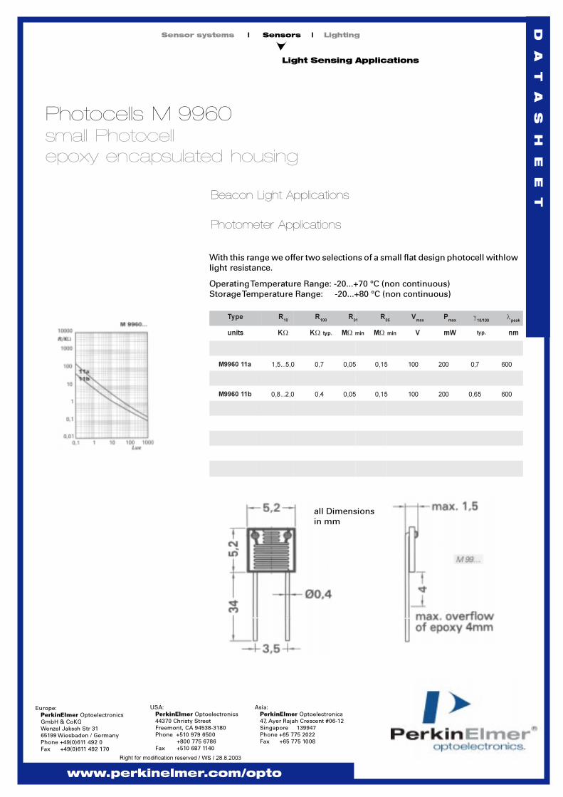
TBeacon Light Applications
Photometer Applications
Photocells M 9960
small Photocellepoxy encapsulated housing
With this range we offer two selections of a small flat design photocell withlow
light resistance.
Operating Temperature Range: -20...+70 °C (non continuous)
Storage Temperature Range: -20...+80 °C (non continuous)
all Dimensions
in mm
a110699M 0,5...5,1 7,0 50,0 51,0 001 002 7,0 006
b110699M 0,2...8,0 4,0 50,0 51,0 001 002 56,0 006
Light Sensing Applications
pSensor systems | Sensors | Lighting
epyT R01
R001
R10
R50
Vxam
Pxam
g001/01
lkaep
stinu KW KW .pyt MW nim MW nim V Wm .pyt mn
29.06.2007
Photocell M996011A
0,01
0,1
1
10
1 10 100 1000 10000
LUX
R / k
Oh
m
Prof. Dr. F. Dildey Dipl.-Ing. J.-C. Böhmke Fakultät Life Sciences
Praktikum Elektronik 2 Versuch 2
Digitale Schaltnetze
- 1 von 4 - Version 1.0 Stand WS 2012 / 2013
1. Lernziel Dieser Versuch soll Ihnen einen Einblick in die Grundlagen der Digitaltechnik vermitteln. Sie werden aus der Gruppe der digitalen Schaltnetze integrierte digitale Bausteine der CMOS-Familie kennen lernen und den Umgang mit den Datenblättern üben. Der Weg von der booleschen Gleichung bis zur Umsetzung in eine funktionsfähige Schaltung soll vermittelt werden.
2. Allgemeines
Schauen Sie in die Datenblätter und machen Sie sich mit den Funktionen und der Pinbelegung der einzelnen Bausteine vertraut. Obwohl die Hersteller zum Teil verschiedene Bezeichnungen für die Bauelemente verwenden, sind die Bauelemente pin- und funktionskompatibel.
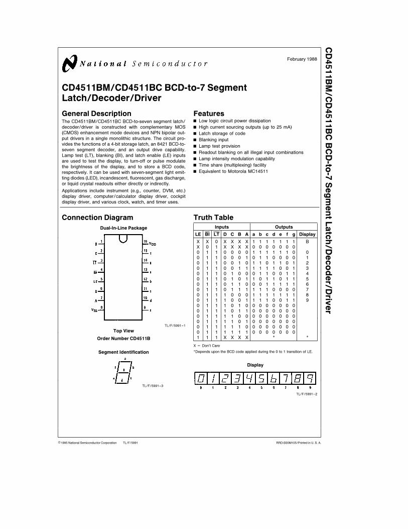
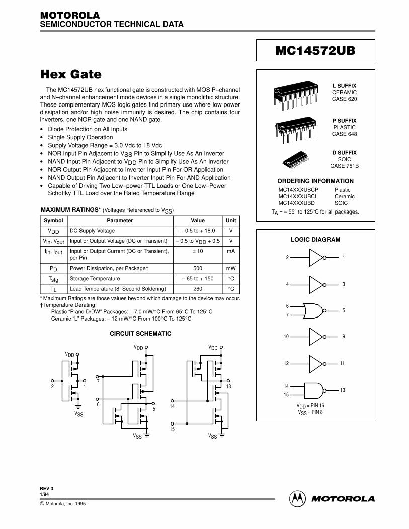
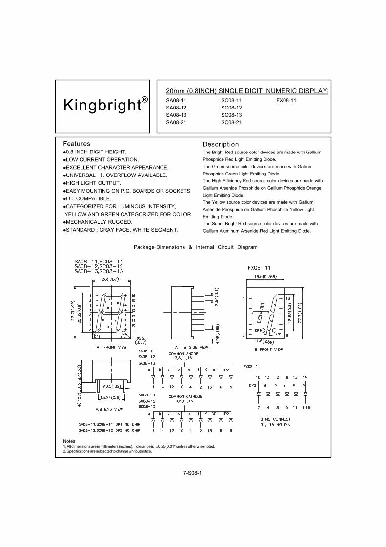
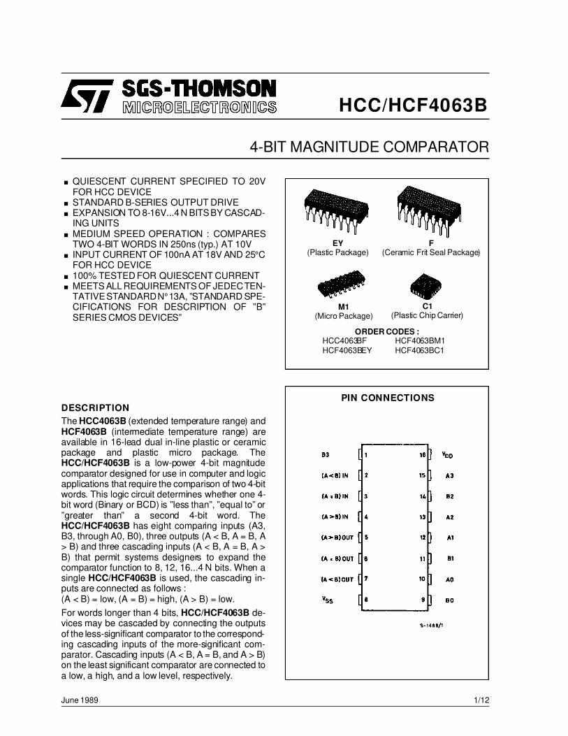
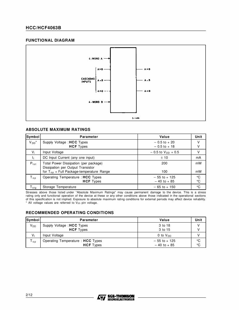
• CD4572 (MC14572UB) Hex Gate, NOR, NAND, NOT • CD4008 (HEF4008B, MC14008B) 4-Bit Binary Full Adder • CD4063 (HCF4063B) 4-Bit Magnitude Comparator • CD4555 (HEF4555B) Dual 1-of-4 Decoder • CD4511 BCD-to-7Segment Decoder / Driver • SC08_11 7-Segment Display
Sie finden die vollständigen Datenblätter auch auf der Laborhomepage.
Als Versorgungsspannung soll aus praktischen Gründen 5 V gewählt werden. Auch höhere
Spannungen sind möglich (bis 15 V), aber die angeschlossenen Leuchtdioden können dann zerstört
werden. In der Praxis werden hochintegrierte Schaltungen heute mit einer Versorgungsspannung von
5 V und kleiner betrieben.
Die Eingangsspannungen dürfen keine negativen Anteile aufweisen!
Wenn die Schaltungen mit dem Funktionsgenerator angesteuert werden, so ist der Ausgang
„TRIG OUTP. (TTL)“ zu benutzen. An diesem Ausgang werden Signale mit TTL-Pegel bereitgestellt.
Es muss darauf geachtet werden, dass die ICs nur im spannungsfreien Zustand eingesetzt bzw.
herausgenommen werden. Beim Herausnehmen ist unter Zuhilfenahme eines speziellen Werkzeuges
das IC vorsichtig aus dem Sockel zu hebeln. Bei CMOS - Bausteinen ist die Handhabung aufgrund des
sehr hohen Eingangswiderstandes (≈1014 Ω) und der Möglichkeit zur Zerstörung der Gate Oxid - Zone
im IC durch statische Entladungen kritisch.
Ein Hersteller gibt folgende Hinweise:
(hier nur auszugsweise wiedergegeben)
1. Personen, die mit CMOS Bausteinen arbeiten, sollten über einen Widerstand geerdet sein.
(Auf diese Maßnahme wird im Praktikum verzichtet).
2. Die ICs sollten nicht unter Spannung eingesetzt oder herausgenommen werden.
3. Vor dem Anlegen der Signalspannungen muss die Versorgungsspannung angeschlossen werden.
4. Alle nicht benutzten Eingänge sollten je nach Funktion auf Masse oder an die
Versorgungsspannung (VDD) angeschlossen sein.
5. Die Bekleidung der Personen, die mit CMOS - Bausteinen umgehen, sollte aus nichtelektrostatischem Material bestehen.
(Auf diese Maßnahme wird im Praktikum verzichtet).
6. Der Transport der ICs sollte nur in der Originalverpackung oder so durchgeführt werden, dass alle
Anschlüsse über ein leitendes Material miteinander verbunden und vor Berührung sicher sind.

Prof. Dr. F. Dildey Dipl.-Ing. J.-C. Böhmke Fakultät Life Sciences
Praktikum Elektronik 2 Versuch 2
Digitale Schaltnetze
- 2 von 4 - Version 1.0 Stand WS 2012 / 2013
3. Vorbereitung
3.1 Begriffe
Zur Vorbereitung dieses Versuches müssen Sie sich über folgende Begriffe in Kenntnis setzen: • CMOS-Technologie • AND, OR, NAND, NOR, NOT - Gatter • Boolesche Algebra • Volladdierer • Komparator • Decoder/Demultiplexer • 7-Segment Display
3.2 Aufgaben zur Vorbereitung des Praktikums
Die Schaltungsentwürfe und Rechenergebnisse sind bei Praktikumsbeginn vorzulegen. Zu allen Aufgaben ist ein vollständiges Schaltbild zu zeichnen. Dabei sind in den Schaltbildern die Anschlüsse mit den entsprechenden Pin-Nummern zu versehen. Benutzen Sie hierfür die Lösungsbögen im Anhang. 3.2.1 Entwerfen Sie mit dem Baustein MC14572 ein 3-fach AND Gatter. Stellen Sie die vollständige
boolesche Gleichung auf, wobei alle benötigten Gatter berücksichtigt sind. 3.2.2 Erstellen Sie eine Wahrheitstabelle für folgende Bedingungen: Wenn die Tür offen (T=0) ist, oder das Fenster offen (F=0) ist und es Nacht (N=1) ist, dann soll ein
Alarm (A=1) ausgelöst werden. Entwickeln Sie nun die boolesche Gleichung. Formen Sie die Gleichung so um, dass sie mit dem
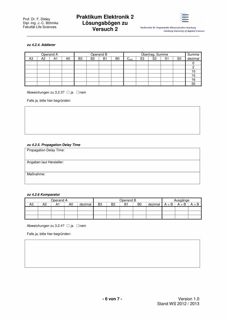
Baustein MC14572 realisiert werden kann. 3.2.3 Erstellen Sie eine Tabelle zum Addieren der 4-Bit-Operanden A und B mit dem IC HEF4008B in
binärer Schreibweise. Formulieren Sie je ein Beispiel für eine Addition, deren Ergebnisse dezimal 0,2,10,15,16, und 30 lauten.
3.2.4. Entwerfen Sie eine Schaltung mit dem Komparator HCF 4063. Stellen Sie eine Tabelle mit den 4-Bit -
Operanden A und B in dezimaler und binärer Schreibweise auf. Dabei sollen alle möglichen Ausgangs-zustände vorkommen. Die „cascading inputs“ werden nur für Zahlen größer als 4 Bit benötigt und müssen hier mit 0 – 1 – 0 beschaltet werden.
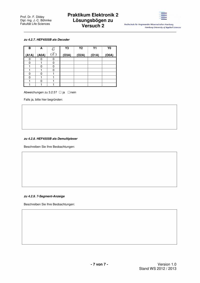
3.2.5. Entwerfen Sie eine Schaltung mit dem Baustein HEF4555B als Decoder. Stellen Sie eine Tabelle mit
den Operanden A0, A1 und (auch häufig genannt) in binärer Schreibweise auf. Dabei sollen alle vorkommenden Ausgangszustände berücksichtigt werden.
3.2.6. Entwerfen Sie eine Schaltung mit dem Baustein HEF4555B als Demultiplexer. Erläutern Sie die Funktionsweise Ihrer Schaltung. An welchen Pin müssen in diesem Fall die zu übertragenden Daten angeschlossen werden?
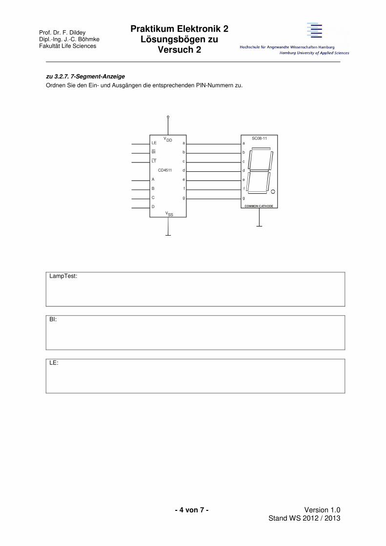
3.2.7 Entwerfen Sie eine Schaltung mit dem Baustein CD4511 und einer 7-Segment Anzeige vom Typ
SC08-11. Alle Anschlusspins sind in der Skizze mit den entsprechenden Nummern zu versehen.
Wie wird ein sogenannter durchgeführt und was erscheint dabei auf der Anzeige? Was bewirkt der Eingang ? Erklären Sie in kurzen Stichworten, wie der Eingang wirkt.
E G
LampTestBL
LE
Prof. Dr. F. Dildey Dipl.-Ing. J.-C. Böhmke Fakultät Life Sciences
Praktikum Elektronik 2 Versuch 2
Digitale Schaltnetze
- 3 von 4 - Version 1.0 Stand WS 2012 / 2013
4. Versuchsdurchführung
4.1 Hinweise zum Schaltungsaufbau
Stellen Sie vor dem Anschließen der Platine die Versorgungsspannung auf +5 V ein.
Stecken Sie das IC in den Sockel und legen Sie nun die Versorgungsspannung an die Platine. (Die Spannungsversorgung für das IC ist in den folgenden Schaltbildern nicht mitgezeichnet).
Benutzen Sie für die logischen Eingaben die Schalter und für die Ausgaben die LEDs. Achten Sie dabei auf eine sinnvolle Beschaltung hinsichtlich der Wertigkeit ihrer Größen. Es macht Sinn, die Wertigkeit (23-22-21-20) so auf die Ein-Ausgabe-Elemente zu legen, das die niederwertigen Bits unten bzw. rechts angeordnet sind.
4.2 Messaufgaben
4.2.1 Für ihre ersten digitalen Gehversuche benutzen Sie den CMOS-Baustein MC14572UB. Beschalten Sie
das NOR-Gatter und das NAND-Gatter (Schalter am Eingang, Leuchtdioden am Ausgang) und nehmen Sie die Wahrheitstabellen auf. Tragen Sie in die letzte Spalte die Negation ein.
4.2.2 Bauen Sie mit dem CMOS-Baustein MC14572UB ihre Schaltung nach 3.2.2. auf. Überprüfen Sie die Schaltung indem Sie die Wahrheitstabelle aufnehmen. 4.2.3 Nehmen Sie die Kennlinie Uout = f(Uin) von einem Inverter des MC14572 auf. Achten Sie darauf, dass am Ausgang keine LED angeschlossen ist. Wichtig: Diese Messung erfolgt zu Testzwecken. In der Praxis dürfen digitale Schaltungen nur
mit digitalen Signalen betrieben werden.
In welchen Spannungsintervallen darf Uin liegen, damit der Ausgang eindeutig die Signale Uout = L und Uout = H annimmt? Welcher Spannungsbereich muss für die Eingangsspannung verboten werden?
4.2.4 Bauen Sie eine Schaltung mit dem Voll-Addierer HEF4008B auf. Überprüfen Sie die Additions-Ergebnisse aus 3.2.3. Tragen Sie abweichende Werte in die Tabelle ein.
Gab es Abweichungen? Woran lag das?
4.2.5 Addieren Sie A = 15 + B. Dabei soll B „0“ oder „1“ sein. Legen Sie den Ausgang vom Funktionsgenerator auf die Variable B0 und messen Sie mit dem Oszilloskop die Zeitdauer der Addition bis zum Übertrag Cout. Dabei sollte keine LED an Cout angeschlossen sein.
Drucken Sie das Bild vom Oszilloskop aus. Verwenden Sie hierzu die Software „OpenChoice Desktop“. Wie groß ist die Propagation Delay Time? Was gibt der Hersteller hierzu im Datenblatt an? Welche Schaltungsmaßnahme im IC beschleunigt die PropDelTime hinsichtlich des Übertrags? 4.2.6 Bauen Sie eine Schaltung mit dem Komparator HCF4063B auf. Überprüfen Sie die Ergebnisse aus
3.2.4 und tragen Sie die Werte in die Tabelle ein.
Gab es Abweichungen? Woran lag das?
4.2.7 Bauen Sie eine Schaltung mit dem Decoder HCF4555B auf. Stellen Sie die Wahrheitstabelle für alle acht Eingangsmöglichkeiten auf. Überprüfen Sie die Ergebnisse aus 3.2.5.
4.2.8 Bauen Sie eine Schaltung mit dem Demultiplexer HCF4555B auf. Legen Sie ein niederfrequentes Rechtecksignal (TRIG OUTP. (TTL)) auf den - bzw. - Eingang. Schalten Sie dieses Signal nacheinander auf die einzelnen Ausgänge O0A, O1A, O2A und O3A und überprüfen Sie Ihre Überlegungen aus 3.2.6.
Wie könnte man aus dieser Schaltung ein laufendes Blinklicht erzeugen?
E G
Prof. Dr. F. Dildey Dipl.-Ing. J.-C. Böhmke Fakultät Life Sciences
Praktikum Elektronik 2 Versuch 2
Digitale Schaltnetze
- 4 von 4 - Version 1.0 Stand WS 2012 / 2013
4.2.9 Bauen Sie eine Schaltung mit dem BCD Decoder CD4511 und einer 7 Segment Anzeige vom Typ
SC08-11 auf.
Führen Sie einen LampTest durch. Nur wenn alle Segmente leuchten, können Sie im Versuch weitergehen, sonst den Fehler suchen.
- Geben sie über den Dekoder verschiedene Zahlen auf das Display (Latch enable = 0). - Geben sie über den Dekoder verschiedene Zahlen auf das Display ( Latch enable = 1 und 0).
Wozu könnte die LE - Funktion dienen? Nennen Sie ein Beispiel.
5. Anhang
5.2 Geräteliste
1x Versuchsplatine DIGI16 mit den ICs:
- MC14572UB (CD4572UB) - HEF4008B - HCF4063B (CD4063BE) - HEF4555B (HCF4555BE) - CD4511 - SC08_11
1x Oszilloskop Tektronix Typ TDS 2002C 1x Dreifachnetzgerät HAMEG Typ HM 7042-5 1x Funktionsgenerator HAMEG Typ HM 8030-6 1x Einbaumultimeter HAMEG Typ HM 8012 2x Handmultimeter Fluke 83 oder 83V
5.3 Literaturhinweise
Formelsammlung zur Vorlesung Elektronik2 von Prof. Dr. Dildey
Tietze/Schenk Halbleiterschaltungstechnik Springer Verlag ISBN 3-540-42849-6
E. Hering K. Bressle J. Gutekunst Elektronik für Ingenieure Springer Verlag ISBN 3-540-41738-9
Folgende Geräteanleitungen finden Sie auf der Laborhomepage: Fluke Multimeter Typ 83, 83/V, 87/III, 179 Tektronix Oszilloskop TDS 2002C HAMEG Labornetzgerät HM7042-5 HAMEG Multimeter HM8012 HAMEG Funktionsgenerator HM 8030-6
5.4 Lösungsbögen und Datenblätter
Lösungsbögen und Datenblätter folgen auf den nächsten Seiten…
Prof. Dr. F. Dildey Dipl.-Ing. J.-C. Böhmke Fakultät Life Sciences
Praktikum Elektronik 2 Lösungsbögen zu
Versuch 2
- 1 von 7 - Version 1.0 Stand WS 2012 / 2013
U1
NOT
U2
NOT
U3
NOT
U4
NOT
U5
NAND2
&
U6
NOR2
>=1
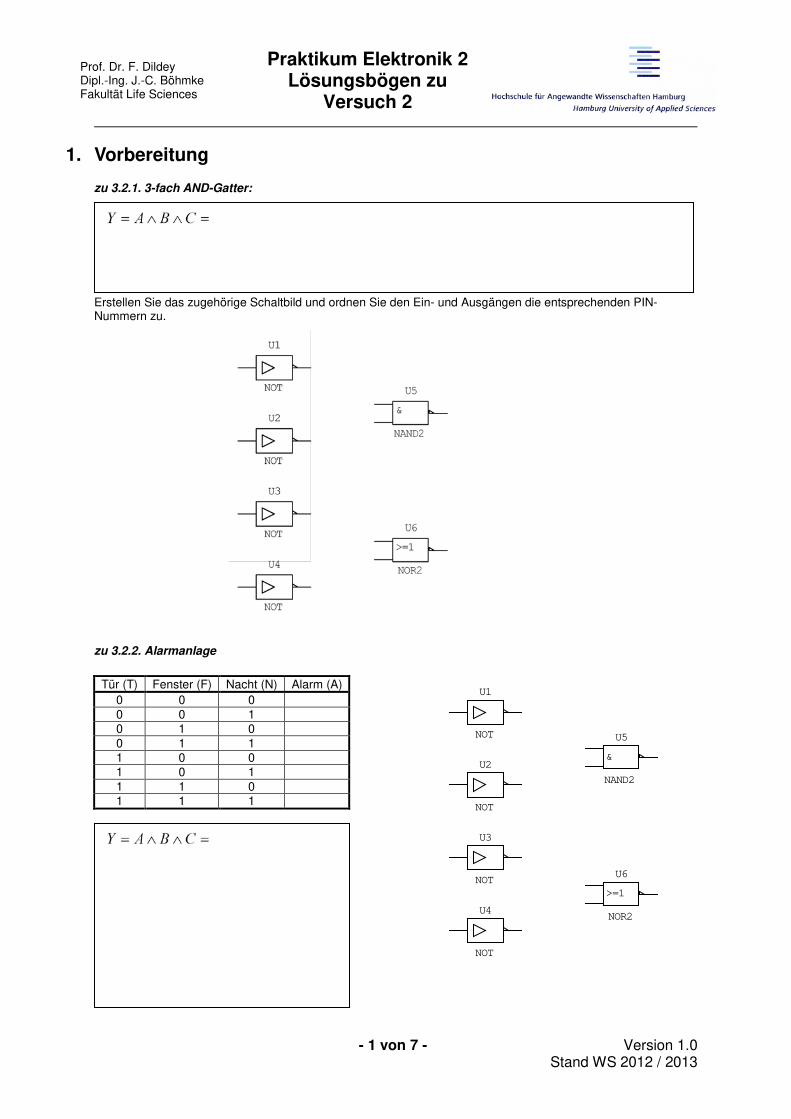
1. Vorbereitung
zu 3.2.1. 3-fach AND-Gatter:
Erstellen Sie das zugehörige Schaltbild und ordnen Sie den Ein- und Ausgängen die entsprechenden PIN-Nummern zu.
zu 3.2.2. Alarmanlage
Tür (T) Fenster (F) Nacht (N) Alarm (A)
0 0 0 0 0 1 0 1 0 0 1 1 1 0 0 1 0 1 1 1 0 1 1 1
Prof. Dr. F. Dildey Dipl.-Ing. J.-C. Böhmke Fakultät Life Sciences
Praktikum Elektronik 2 Lösungsbögen zu
Versuch 2
- 2 von 7 - Version 1.0 Stand WS 2012 / 2013
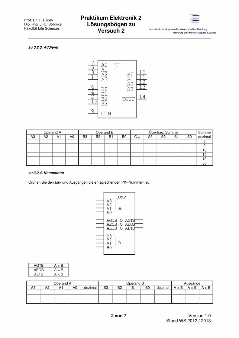
zu 3.2.3. Addierer
Operand A Operand B Übertrag, Summe Summe A3 A2 A1 A0 B3 B2 B1 B0 Cout S3 S2 S1 S0 dezimal
0 2 10 15 16
30
zu 3.2.4. Komparator
Ordnen Sie den Ein- und Ausgängen die entsprechenden PIN-Nummern zu.
AGTB A > B AEQB A = B ALTB A < B
Operand A Operand B Ausgänge
A3 A2 A1 A0 dezimal B3 B2 B1 B0 dezimal A < B A = B A > B
COMP
A
B
A2
B2
A1
B1
O_AGTB
A0
B0
A3
B3
O_AEQBO_ALTB
AEQBAGTB
ALTB
Prof. Dr. F. Dildey Dipl.-Ing. J.-C. Böhmke Fakultät Life Sciences
Praktikum Elektronik 2 Lösungsbögen zu
Versuch 2
- 3 von 7 - Version 1.0 Stand WS 2012 / 2013
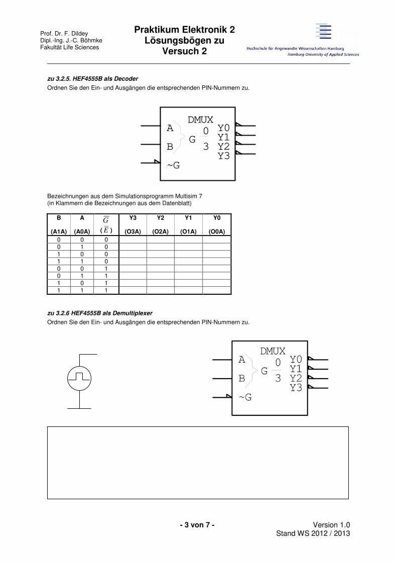
zu 3.2.5. HEF4555B als Decoder
Ordnen Sie den Ein- und Ausgängen die entsprechenden PIN-Nummern zu.
Bezeichnungen aus dem Simulationsprogramm Multisim 7 (in Klammern die Bezeichnungen aus dem Datenblatt)
B
(A1A)
A
(A0A)
G
( E )
Y3
(O3A)
Y2
(O2A)
Y1
(O1A)
Y0
(O0A)
0 0 0 0 1 0 1 0 0 1 1 0 0 0 1 0 1 1 1 0 1 1 1 1
zu 3.2.6 HEF4555B als Demultiplexer
Ordnen Sie den Ein- und Ausgängen die entsprechenden PIN-Nummern zu.
DMUX
G0
3
Y0Y1Y2Y3
~G
A
B
Prof. Dr. F. Dildey Dipl.-Ing. J.-C. Böhmke Fakultät Life Sciences
Praktikum Elektronik 2 Lösungsbögen zu
Versuch 2
- 4 von 7 - Version 1.0 Stand WS 2012 / 2013
zu 3.2.7. 7-Segment-Anzeige
Ordnen Sie den Ein- und Ausgängen die entsprechenden PIN-Nummern zu.
VDDLE
A
B
C
D
VSS
a a
b b
c c
d d
e e
f f
g g
COMMON CATHODE
SC08-11
CD4511
BI
LT
LampTest:
BI:
LE:
Prof. Dr. F. Dildey Dipl.-Ing. J.-C. Böhmke Fakultät Life Sciences
Praktikum Elektronik 2 Lösungsbögen zu
Versuch 2
- 5 von 7 - Version 1.0 Stand WS 2012 / 2013
2. Versuchsdurchführung
zu 4.2.1. 3-fach AND-Gatter
NOR NAND
X1 X2 Y Y (OR) X1 X2 Y Y (AND)
AND X1 X2 X3 Y 0 0 0 0 0 1 0 1 0 0 1 1 1 0 0 1 0 1 1 1 0 1 1 1
zu 4.2.2. Alarmanlage
Tür (T) Fenster (F) Nacht (N) Alarm (A)
0 0 0 0 0 1 0 1 0 0 1 1 1 0 0 1 0 1 1 1 0 1 1 1
zu 4.2.3. verbotener Bereich
Werten Sie Ihre Tabelle mit MS Excel aus.
Uin Uout 0,0 1,0 1,5 2,0 2,1 2,2 2,3 2,4 2,5 2,6 2,7 2,8 2,9 3,0 3,5 4,0 5,0
Verbotener Bereich:
Prof. Dr. F. Dildey Dipl.-Ing. J.-C. Böhmke Fakultät Life Sciences
Praktikum Elektronik 2 Lösungsbögen zu
Versuch 2
- 6 von 7 - Version 1.0 Stand WS 2012 / 2013
zu 4.2.4. Addierer
Operand A Operand B Übertrag, Summe Summe
A3 A2 A1 A0 B3 B2 B1 B0 Cout S3 S2 S1 S0 dezimal 0 2 10 15 16
30 Abweichungen zu 3.2.3? ja nein Falls ja, bitte hier begründen:
zu 4.2.5. Propagation Delay Time
Propagation Delay Time: Angaben laut Hersteller: Maßnahme:
zu 4.2.6 Komparator
Operand A Operand B Ausgänge A3 A2 A1 A0 dezimal B3 B2 B1 B0 dezimal A < B A = B A > B
Abweichungen zu 3.2.4? ja nein Falls ja, bitte hier begründen:
Prof. Dr. F. Dildey Dipl.-Ing. J.-C. Böhmke Fakultät Life Sciences
Praktikum Elektronik 2 Lösungsbögen zu
Versuch 2
- 7 von 7 - Version 1.0 Stand WS 2012 / 2013
zu 4.2.7. HEF4555B als Decoder
B
(A1A)
A
(A0A)
G
( E )
Y3
(O3A)
Y2
(O2A)
Y1
(O1A)
Y0
(O0A)
0 0 0 0 1 0 1 0 0 1 1 0 0 0 1 0 1 1 1 0 1 1 1 1
Abweichungen zu 3.2.5? ja nein Falls ja, bitte hier begründen:
zu 4.2.8. HEF4555B als Demultiplexer
Beschreiben Sie Ihre Beobachtungen:
zu 4.2.9. 7-Segment-Anzeige
Beschreiben Sie Ihre Beobachtungen:

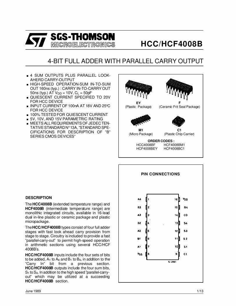
HCC/HCF4008B
4-BIT FULL ADDER WITH PARALLEL CARRY OUTPUT
DESCRIPTION
. 4 SUM OUTPUTS PLUS PARALLEL LOOK-AHERD CARRY-OUTPUT.HIGH-SPEED OPERATION-SUM IN-TO-SUMOUT 160ns (typ.) : CARRY IN-TO-CARRY OUT50ns (typ.) AT VDD = 10V, CL = 50pF.QUIESCENT CURRENT SPECIFIED TO 20VFOR HCC DEVICE. INPUT CURRENT OF 100nA AT 18V AND 25°CFOR HCC DEVICE. 100% TESTED FOR QUIESCENT CURRENT. 5V, 10V, AND 15V PARAMETRIC RATING.MEETS ALL REQUIREMENTS OF JEDECTEN-TATIVESTANDARDN°13A, ”STANDARD SPE-CIFICATIONS FOR DESCRIPTION OF ”B”SERIES CMOS DEVICES”
June 1989
The HCC4008B (extended temperature range) andHCF4008B (intermediate temperature range) aremonolithic integrated circuits, available in 16-leaddual in-line plastic or ceramic package and plasticmicropackage.
TheHCC/HCF4008B types consist of four full adderstages with fast look ahead carry provision fromstage to stage. Circuitry is included to provide a fast”parallel-carry-out” to permit high-speed operationin arithmetic sections using several HCC/HCF4008B’s.
HCC/HCF4008B inputs include the four sets of bitsto be added, A1 to A4 and B1 to B4, in addition to the”Carry In” bit from a previous section.HCC/HCF4008B outputs include the four sum bits,S1 toS4. Inaddition to the high speed ”parallel-carry-out” which may be utilized at a succeedingHCC/HCF4008B section.
EY(Plastic Package)
F(Ceramic Frit Seal Package)
C1(Plastic Chip Carrier)
ORDER CODES :HCC4008BF HCF4008BM1HCF4008BEY HCF4008BC1
PIN CONNECTIONS
M1(Micro Package)
1/13
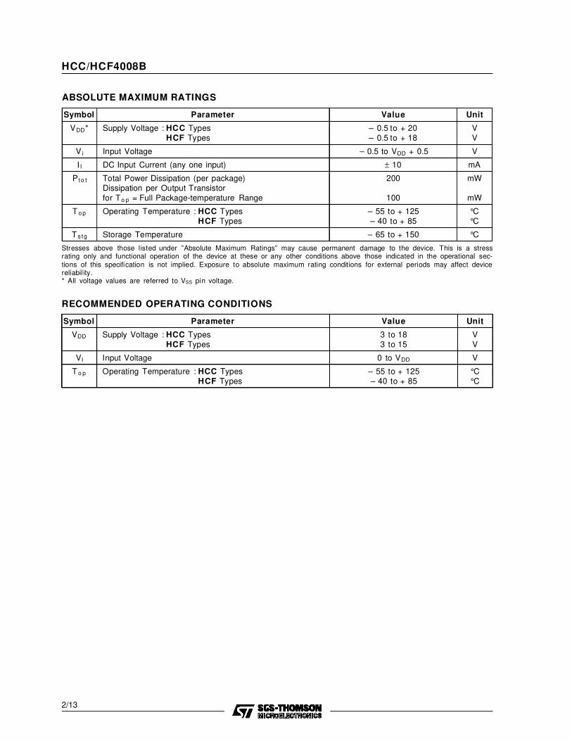
ABSOLUTE MAXIMUM RATINGS
Symbol Parameter Value Unit
VDD* Supply Voltage : HCC TypesHCF Types
– 0.5 to + 20– 0.5 to + 18
VV
V i Input Voltage – 0.5 to VDD + 0.5 V
I I DC Input Current (any one input) ± 10 mA
P t o t Total Power Dissipation (per package)Dissipation per Output Transistorfor To p = Full Package-temperature Range
200
100
mW
mW
T o p Operating Temperature : HCC TypesHCF Types
– 55 to + 125– 40 to + 85
°C°C
T s tg Storage Temperature – 65 to + 150 °C
RECOMMENDED OPERATING CONDITIONS
Symbol Parameter Value Unit
VDD Supply Voltage : HCC TypesHCF Types
3 to 183 to 15
VV
VI Input Voltage 0 to VDD V
T o p Operating Temperature : HCC TypesHCF Types
– 55 to + 125– 40 to + 85
°C°C
Stresses above those listed under ”Absolute Maximum Ratings” may cause permanent damage to the device. This is a stressrating only and functional operation of the device at these or any other conditions above those indicated in the operational sec-tions of this specification is not implied. Exposure to absolute maximum rating conditions for external periods may affect devicereliabil ity.* All voltage values are referred to VSS pin voltage.
HCC/HCF4008B
2/13
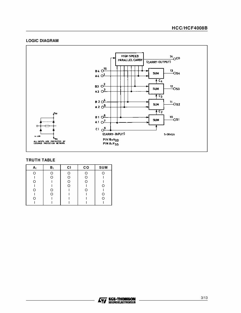
LOGIC DIAGRAM
TRUTH TABLE
A i B i CI C O SUM
OI
OI
OI
OI
OO
II
OO
II
OO
OO
II
II
OO
OI
OI
II
OI
IO
IO
OI
HCC/HCF4008B
3/13
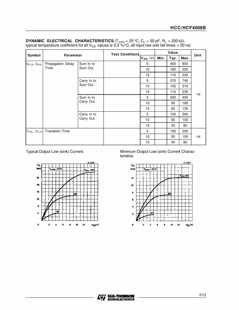
DYNAMIC ELECTRICAL CHARACTERISTICS (Tamb = 25 °C, CL = 50 pF, RL = 200 kΩ,typical temperature coefficient for all VDD values is 0.3 %/°C, all input rise and fall times = 20 ns)
ValueSymbol Parameter Test Conditions
V D D (V) Min. Typ. Max.Unit
tP L H, tP HL Propagation Delay
Time
Sum In to
Sum Out
5 400 800
ns
10 160 320
15 115 230
Carry In toSum Out
5 370 740
10 155 310
15 115 230
Sum In toCarry Out
5 200 400
10 90 180
15 65 130
Carry In to
Carry Out
5 100 200
10 50 100
15 40 80
tTHL , tT L H Transition Time 5 100 200
ns10 50 100
15 40 80
Minimum Output Low (sink) Current Charac-teristics.
Typical Output Low (sink) Current.
HCC/HCF4008B
5/13
TL/F/5991
CD
4511B
M/C
D4511B
CB
CD
-to-7
Segm
entLatc
h/D
ecoder/
Driv
er
February 1988
CD4511BM/CD4511BC BCD-to-7 SegmentLatch/Decoder/Driver
General DescriptionThe CD4511BM/CD4511BC BCD-to-seven segment latch/
decoder/driver is constructed with complementary MOS
(CMOS) enhancement mode devices and NPN bipolar out-
put drivers in a single monolithic structure. The circuit pro-
vides the functions of a 4-bit storage latch, an 8421 BCD-to-
seven segment decoder, and an output drive capability.
Lamp test (LT), blanking (BI), and latch enable (LE) inputs
are used to test the display, to turn-off or pulse modulate
the brightness of the display, and to store a BCD code,
respectively. It can be used with seven-segment light emit-
ting diodes (LED), incandescent, fluorescent, gas discharge,
or liquid crystal readouts either directly or indirectly.
Applications include instrument (e.g., counter, DVM, etc.)
display driver, computer/calculator display driver, cockpit
display driver, and various clock, watch, and timer uses.
FeaturesY Low logic circuit power dissipationY High current sourcing outputs (up to 25 mA)Y Latch storage of codeY Blanking inputY Lamp test provisionY Readout blanking on all illegal input combinationsY Lamp intensity modulation capabilityY Time share (multiplexing) facilityY Equivalent to Motorola MC14511
Connection Diagram
Dual-In-Line Package
TL/F/5991–1
Top View
Order Number CD4511B
Segment Identification
TL/F/5991–3
Truth Table
Inputs Outputs
LE BI LT D C B A a b c d e f g Display
X X 0 X X X X 1 1 1 1 1 1 1 BX 0 1 X X X X 0 0 0 0 0 0 00 1 1 0 0 0 0 1 1 1 1 1 1 0 00 1 1 0 0 0 1 0 1 1 0 0 0 0 10 1 1 0 0 1 0 1 1 0 1 1 0 1 20 1 1 0 0 1 1 1 1 1 1 0 0 1 30 1 1 0 1 0 0 0 1 1 0 0 1 1 40 1 1 0 1 0 1 1 0 1 1 0 1 1 50 1 1 0 1 1 0 0 0 1 1 1 1 1 60 1 1 0 1 1 1 1 1 1 0 0 0 0 70 1 1 1 0 0 0 1 1 1 1 1 1 1 80 1 1 1 0 0 1 1 1 1 0 0 1 1 90 1 1 1 0 1 0 0 0 0 0 0 0 00 1 1 1 0 1 1 0 0 0 0 0 0 00 1 1 1 1 0 0 0 0 0 0 0 0 00 1 1 1 1 0 1 0 0 0 0 0 0 00 1 1 1 1 1 0 0 0 0 0 0 0 00 1 1 1 1 1 1 0 0 0 0 0 0 01 1 1 X X X X * *
X e Don’t Care
*Depends upon the BCD code applied during the 0 to 1 transition of LE.
Display
TL/F/5991–2
C1995 National Semiconductor Corporation RRD-B30M105/Printed in U. S. A.
MOTOROLA CMOS LOGIC DATA1
MC14572UB
The MC14572UB hex functional gate is constructed with MOS P–channel
and N–channel enhancement mode devices in a single monolithic structure.These complementary MOS logic gates find primary use where low power
dissipation and/or high noise immunity is desired. The chip contains fourinverters, one NOR gate and one NAND gate.
• Diode Protection on All Inputs
• Single Supply Operation
• Supply Voltage Range = 3.0 Vdc to 18 Vdc
• NOR Input Pin Adjacent to VSS Pin to Simplify Use As An Inverter
• NAND Input Pin Adjacent to VDD Pin to Simplify Use As An Inverter
• NOR Output Pin Adjacent to Inverter Input Pin For OR Application
• NAND Output Pin Adjacent to Inverter Input Pin For AND Application
• Capable of Driving Two Low–power TTL Loads or One Low–Power
Schottky TTL Load over the Rated Temperature RangeÎÎÎÎÎÎÎÎÎÎÎÎÎÎÎÎÎÎÎÎÎ
ÎÎÎÎÎÎÎÎÎÎÎÎÎÎÎÎÎÎÎÎÎ
ÎÎÎÎÎÎÎÎÎÎÎÎÎÎÎÎÎÎÎÎÎ
ÎÎÎÎÎÎÎÎÎÎÎÎÎÎÎÎÎÎÎÎÎ
MAXIMUM RATINGS* (Voltages Referenced to VSS)
Symbol Parameter Value Unit
VDD DC Supply Voltage – 0.5 to + 18.0 V
Vin, Vout Input or Output Voltage (DC or Transient) – 0.5 to VDD + 0.5 V
Iin, Iout Input or Output Current (DC or Transient),
per Pin
± 10 mA
PD Power Dissipation, per Package† 500 mW
Tstg Storage Temperature – 65 to + 150 C
TL Lead Temperature (8–Second Soldering) 260 C
* Maximum Ratings are those values beyond which damage to the device may occur.
†Temperature Derating:
Plastic “P and D/DW” Packages: – 7.0 mW/C From 65C To 125C
Ceramic “L” Packages: – 12 mW/C From 100C To 125C
CIRCUIT SCHEMATIC
VDD
VDDVDD
27
6
1
5 14
15
13
VSSVSS
VSS
SEMICONDUCTOR TECHNICAL DATA
Motorola, Inc. 1995
REV 3
1/94
L SUFFIX
CERAMIC
CASE 620
ORDERING INFORMATION
MC14XXXUBCP Plastic
MC14XXXUBCL Ceramic
MC14XXXUBD SOIC
TA = – 55° to 125°C for all packages.
P SUFFIX
PLASTIC
CASE 648
D SUFFIX
SOIC
CASE 751B
LOGIC DIAGRAM
15
14
12
10
7
6
4
2
13
11
9
5
3
1
VDD = PIN 16
VSS = PIN 8
7-S08-1
Kingbright®
Features
0.8 INCH DIGIT HEIGHT.
LOW CURRENT OPERATION.
EXCELLENT CHARACTER APPEARANCE.
UNIVERSAL . OVERFLOW AVAILABLE.
HIGH LIGHT OUTPUT.
EASY MOUNTING ON P.C. BOARDS OR SOCKETS.
I.C. COMPATIBLE.
CATEGORIZED FOR LUMINOUS INTENSITY,
YELLOW AND GREEN CATEGORIZED FOR COLOR.
MECHANICALLY RUGGED.
STANDARD : GRAY FACE, WHITE SEGMENT.
Package Dimensions & Internal Circuit Diagram
DescriptionThe Bright Red source color devices are made with Gallium
Phosphide Red Light Emitting Diode.
The Green source color devices are made with Gallium
Phosphide Green Light Emitting Diode.
The High Efficiency Red source color devices are made with
Gallium Arsenide Phosphide on Gallium Phosphide Orange
Light Emitting Diode.
The Yellow source color devices are made with Gallium
Arsenide Phosphide on Gallium Phosphide Yellow Light
Emitting Diode.
The Super Bright Red source color devices are made with
Gallium Aluminum Arsenide Red Light Emitting Diode.
20mm (0.8INCH) SINGLE DIGIT NUMERIC DISPLAYS
SA08-11 SC08-11 FX08-11
SA08-12 SC08-12
SA08-13 SC08-13
SA08-21 SC08-21
Notes:1. All dimensions are in millimeters (inches), Tolerance is ±0.25(0.01")unless otherwise noted.
2. Specifications are subjected to change whitout notice.
HCC/HCF4063B
June 1989
4-BIT MAGNITUDE COMPARATOR
.QUIESCENT CURRENT SPECIFIED TO 20VFOR HCC DEVICE.STANDARD B-SERIES OUTPUT DRIVE.EXPANSION TO 8-16V...4 N BITSBY CASCAD-ING UNITS.MEDIUM SPEED OPERATION : COMPARESTWO 4-BIT WORDS IN 250ns (typ.) AT 10V. INPUT CURRENT OF 100nA AT 18V AND 25°CFOR HCC DEVICE. 100% TESTED FOR QUIESCENT CURRENT.MEETS ALL REQUIREMENTS OF JEDECTEN-TATIVESTANDARDN°13A, ”STANDARD SPE-CIFICATIONS FOR DESCRIPTION OF ”B”SERIES CMOS DEVICES”
DESCRIPTION
The HCC4063B (extended temperature range) andHCF4063B (intermediate temperature range) areavailable in 16-lead dual in-line plastic or ceramicpackage and plastic micro package. TheHCC/HCF4063B is a low-power 4-bit magnitudecomparator designed for use in computer and logicapplications that require the comparison of two 4-bitwords. This logic circuit determines whether one 4-bit word (Binary or BCD) is ”less than”, ”equal to” or”greater than” a second 4-bit word. TheHCC/HCF4063B has eight comparing inputs (A3,B3, through A0, B0), three outputs (A < B, A = B, A> B) and three cascading inputs (A < B, A = B, A >B) that permit systems designers to expand thecomparator function to 8, 12, 16...4 N bits. When asingle HCC/HCF4063B is used, the cascading in-puts are connected as follows :(A < B) = low, (A = B) = high, (A > B) = low.
For words longer than 4 bits, HCC/HCF4063B de-vices may be cascaded by connecting the outputsof the less-significant comparator to the correspond-ing cascading inputs of the more-significant com-parator. Cascading inputs (A < B, A = B, and A > B)on the least significant comparator are connected toa low, a high, and a low level, respectively.
EY(Plastic Package)
F(Ceramic Frit Seal Package)
M1(Micro Package)
C1(Plastic Chip Carrier)
ORDER CODES :HCC4063BF HCF4063BM1HCF4063BEY HCF4063BC1
PIN CONNECTIONS
1/12
ABSOLUTE MAXIMUM RATINGS
Symbol Parameter Value Unit
V DD* Supply Voltage : HCC Types
HCF Types
– 0.5 to + 20
– 0.5 to + 18
V
V
Vi Input Voltage – 0.5 to VDD + 0.5 V
I I DC Input Current (any one input) ± 10 mA
P t o t Total Power Dissipation (per package)
Dissipation per Output Transistorfor To p = Full Package-temperature Range
200
100
mW
mW
T o p Operating Temperature : HCC TypesHCF Types
– 55 to + 125– 40 to + 85
°C°C
Ts tg Storage Temperature – 65 to + 150 °C
Stresses above those listed under ”Absolute Maximum Ratings” may cause permanent damage to the device. This is a stressrating only and functional operation of the device at these or any other conditions above those indicated in the operational sectionsof this specification is not implied. Exposure to absolute maximum rating conditions for external periods may affect device reliability.* All voltage values are referred to VSS pin voltage.
FUNCTIONAL DIAGRAM
RECOMMENDED OPERATING CONDITIONS
Symbol Parameter Value Unit
VDD Supply Voltage : HCC Types
HCF Types
3 to 18
3 to 15
V
V
VI Input Voltage 0 to VDD V
T o p Operating Temperature : HCC Types
HCF Types
– 55 to + 125
– 40 to + 85
°C°C
HCC/HCF4063B
2/12
LOGIC DIAGRAM
TRUTH TABLE
Inputs
Comparing CascadingOutputs
A3, B3 A2, B2 A1, B1 A0, B0 A < B A = B A > B A < B A = B A > B
A3 > B3A3 = B3
A3 = B3A3 = B3
XA2 > B2
A2 = B2A2 = B2
XX
A1 > B1A1 = B1
XX
XA0 > B0
XX
XX
XX
XX
XX
XX
00
00
00
00
11
11
A3 = B3A3 = B3
A3 = B3
A2 = B2A2 = B2
A2 = B2
A1 = B1A1 = B1
A1 = B1
A0 = B0A0 = B0
A0 = B0
00
1
01
0
10
0
00
1
01
0
10
0
A3 = B3
A3 = B3A3 = B3A3 < B3
A2 = B2
A2 = B2A2 < B2
X
A1 = B1
A1 < B1XX
A0 < B0
XXX
X
XXX
X
XXX
X
XXX
1
111
0
000
0
000
X = Don’t care 1 ≡ High state 0 ≡ Low state.
HCC/HCF4063B
3/12
January 1995 2
Philips Semiconductors Product specification
Dual 1-of-4 decoder/demultiplexerHEF4555B
MSI
DESCRIPTION
The HEF4555B is a dual 1-of-4 decoder/demultiplexer.
Each has two address inputs (A0 and A1), an active LOW
enable input (E) and four mutually exclusive outputs which
are active HIGH (O0 to O3). When used as a decoder,
E when HIGH, forces O0 to O3 LOW. When used as a
demultiplexer, the appropriate output is selected by the
information on A0 and A1 with E as data input. All
unselected outputs are LOW.
Fig.1 Functional diagram.
PINNING
FAMILY DATA, IDD LIMITS category MSI
See Family Specifications
HEF4555BP(N): 16-lead DIL; plastic
(SOT38-1)
HEF4555BD(F): 16-lead DIL; ceramic (cerdip)
(SOT74)
HEF4555BT(D): 16-lead SO; plastic
(SOT109-1)
( ): Package Designator North America
E enable inputs (active LOW)
A0 and A1 address inputs
O0 to O3 outputs (active HIGH)
Fig.2 Pinning diagram.
January 1995 3
Philips Semiconductors Product specification
Dual 1-of-4 decoder/demultiplexerHEF4555B
MSI
TRUTH TABLE
Notes
1. H = HIGH state (the more positive voltage)
2. L = LOW state (the less positive voltage)
3. X = state is immaterial
INPUTS OUTPUTS
E A0 A1 O0 O1 O2 O3
L L L H L L L
L H L L H L L
L L H L L H L
L H H L L L H
H X X L L L L
Fig.3 Logic diagram (one decoder/multiplexer).
Prof. Dr. F. Dildey Dipl.-Ing. J.-C. Böhmke Fakultät Life Sciences
Praktikum Elektronik 2 Versuch 3
Digitale Schaltwerke
- 1 von 5 - Version 1.0 Stand WS 2012 / 2013
1. Lernziel
Aufbauend auf den 2. Versuch „Digitale Schaltnetze“ soll Ihr Einblick in die Digitaltechnik vertieft werden.
In diesem Versuch werden digitale Schaltwerke eingesetzt. Im Gegensatz zu den bisher behandelten Schaltnetzen, bei denen definitionsgemäß keine Rückkopplungen vorliegen, ist bei einem Schaltwerk mindestens einer der Ausgänge auf mindestens einen der Eingänge rückgekoppelt, wodurch die Schaltung einen speichernden Charakter (ein Gedächtnis) erhält.
Untersucht werden ein D-Flip-Flop, ein Mono-Flop, ein Zähler und ein Schieberegister. Es soll insbesondere das Verhalten dieser Bausteine im dynamischen Betrieb untersucht werden. Die funktionsgerechte Beschaltung der ICs anhand der Herstellerangaben soll geübt werden.
2. Allgemeines
Schauen Sie in die Datenblätter und machen Sie sich mit den Funktionen und der Pinbelegung der
einzelnen Bausteine vertraut.
Als Versorgungsspannung soll aus praktischen Gründen 5 V gewählt werden. Auch höhere
Spannungen sind möglich (bis 15V), aber die angeschlossenen Leuchtdioden können dann zerstört
werden. In der Praxis werden hochintegrierte Schaltungen heute mit einer Versorgungsspannung von
5 V und kleiner betrieben.
Die Eingangsspannungen dürfen keine negativen Anteile aufweisen!
Wenn die Schaltungen mit dem Funktionsgenerator angesteuert werden, so ist der Ausgang
„TRIG OUTP. (TTL)“ zu benutzen. An diesem Ausgang werden Signale mit TTL-Pegel bereitgestellt.
Es muss darauf geachtet werden, dass die ICs nur im spannungsfreien Zustand eingesetzt bzw.
herausgenommen werden. Beim Herausnehmen ist unter Zuhilfenahme eines speziellen Werkzeuges
das IC vorsichtig aus dem Sockel zu hebeln. Bei CMOS - Bausteinen ist die Handhabung aufgrund des
sehr hohen Eingangswiderstandes (≈1014 Ω) und der Möglichkeit zur Zerstörung der Gate Oxid - Zone
im IC durch statische Entladungen kritisch.
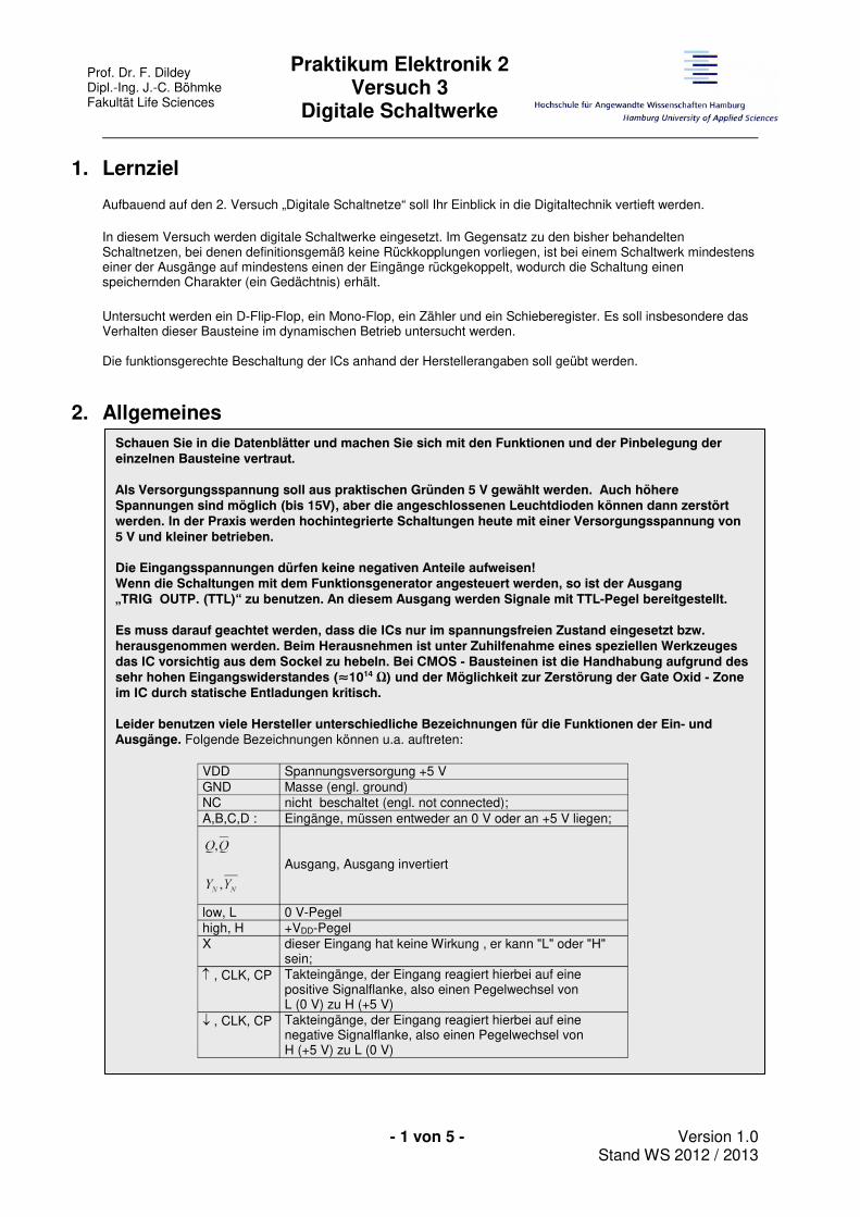
Leider benutzen viele Hersteller unterschiedliche Bezeichnungen für die Funktionen der Ein- und Ausgänge. Folgende Bezeichnungen können u.a. auftreten:
VDD Spannungsversorgung +5 V GND Masse (engl. ground) NC nicht beschaltet (engl. not connected); A,B,C,D : Eingänge, müssen entweder an 0 V oder an +5 V liegen;
Ausgang, Ausgang invertiert
low, L 0 V-Pegel high, H +VDD-Pegel X dieser Eingang hat keine Wirkung , er kann "L" oder "H"
sein; ↑ , CLK, CP Takteingänge, der Eingang reagiert hierbei auf eine
positive Signalflanke, also einen Pegelwechsel von L (0 V) zu H (+5 V)
↓ , CLK, CP Takteingänge, der Eingang reagiert hierbei auf eine negative Signalflanke, also einen Pegelwechsel von H (+5 V) zu L (0 V)
Prof. Dr. F. Dildey Dipl.-Ing. J.-C. Böhmke Fakultät Life Sciences
Praktikum Elektronik 2 Versuch 3
Digitale Schaltwerke
- 2 von 5 - Version 1.0 Stand WS 2012 / 2013
2.1 Funktion der Bauelemente
Im Folgenden werden die Funktionen der verwendeten Bauelemente sowie das Verhalten der jeweiligen Ein- und Ausgänge näher beschrieben. Obwohl sich die Bauteilbezeichnungen der Hersteller zum Teil unterscheiden, sind die Bauelemente dennoch pin- und funktionskompatibel.
2.1.1 Quad-D-Flip-Flop (CD40175, MC14572UB) Dieses IC beinhaltet vier D-Flip-Flops mit einem gemeinsamen Clear- und Clock- Eingang. Der Takt-Eingang (engl. clock) ist positiv flankengetriggert, d.h., die Übernahme der Information am Eingang "D" findet n u r dann statt, wenn das Signal am Takt-Eingang von 0 V auf +VDD wechselt.
2.1.2 Monoflop (4538, CD14538, MC14538B) Eine monostabile Kippstufe, auch Monoflop oder Univibrator genannt, ist eine elektronische Schaltung, die nur einen stabilen Zustand hat. Durch einen äußeren Trigger-Impuls angesteuert, ändert die Schaltung für eine durch ihre Dimensionierung bestimmte Zeit ihren Ausgangszustand, bis sie wieder von selbst in die Ruhelage zurückkehrt. Man unterscheidet zwischen nachtriggerbaren (auch: retriggerbaren) und nicht nachtriggerbaren Monoflops. Nachtriggerbar bedeutet, dass ein während des Zeitablaufes eintreffendes Triggersignal die interne Zeitbasis jeweils erneut startet und der aktive Schaltzustand dementsprechend zeitlich verlängert wird. Bei einem nicht nachtriggerbaren Monoflop hat ein Triggersignal während der aktiven Phase keine Wirkung. Mit dem hier vorgestellten Baustein lassen sich sowohl nachtriggerbare als auch nicht nachtriggerbare Schaltungen realisieren. Hierbei sind Pulsweiten von 10 µs bis 10 s einstellbar.
2.1.3 Presettable binary / decade up / down counter (CD4029B) Über verschiedene Steuereingänge kann dieser Baustein als binärer bzw. dezimaler Auf- bzw. Abwärtszähler konfiguriert werden. Zusätzlich kann ein bestimmter Zählerwert voreingestellt werden. Eine positive Flanke am Takt-Eingang bewirkt, dass der Zähler weiterzählt. Die Steuereingänge vom CD4029 wirken wie folgt:
Eingang PIN Pegel Wirkung UP/DOWN 10 1
0 Zähler zählt aufwärts Zähler zählt abwärts
BINARY/DECADE 9 1 0
Zähler zählt binär, also von 0 bis 15 Zähler zählt dezimal, also von 0 bis 9
PRESET ENABLE
1 1 0
Zähler wird geladen, es wird der an den Eingängen J1...J4 anliegende Zahlenwert übernommen Der aktuelle Zählerzustand wird nicht von den Eingängen J1…J4 verändert.
CARRY IN 5 1 0
Übertrag hinzufügen Keinen Übertrag hinzufügen
CLOCK 15 0>1 Zählt einen Takt weiter
2.1.4 Schieberegister (74HC194, CD74HCT194) Die hier folgenden Beschreibungen der Anschlüsse und der Funktionen beziehen sich auf diesen Baustein. Vom Prinzip her sind die Bezeichnungen aber auf alle Schieberegister übertragbar. ACHTUNG: In den Datenblättern mancher Hersteller sind die Ausgänge Q0 bis Q3 vertauscht. Dort ist dann Q0 der Ausgang mit der Wertigkeit 23. Ein Schieberegister dient zur Speicherung von Informationen. Es kann die digitalen Informationen seriell oder auch parallel aufnehmen, und es kann diese gespeicherten Informationen ebenfalls seriell oder parallel ausgeben.
Prof. Dr. F. Dildey Dipl.-Ing. J.-C. Böhmke Fakultät Life Sciences
Praktikum Elektronik 2 Versuch 3
Digitale Schaltwerke
- 3 von 5 - Version 1.0 Stand WS 2012 / 2013
Die serielle Übernahme des digitalen Musters geschieht getaktet, d.h. mit jedem Taktzyklus am Takteingang (CLK) wird ein Bit vom seriellen Eingang (DSL bzw. DSR, je nach Schieberichtung) in das Register geschoben. Das hier benutzte Schieberegister vom Typ 74HCT194 wäre also nach vier Takten "voll". Die eingeschriebene Information liegt nun parallel an den Ausgängen QA bis QD (auch Q3 bis Q0 genannt) an; es hat eine Seriell-Parallel-Wandlung stattgefunden. Das Register kann aber auch parallel geladen werden. Es arbeitet dabei wie ein vierfaches D-Flip-Flop. Das an den Eingängen A, B, C und D (auch P3 bis P0) anliegende Muster wird mit der positiven Flanke am Takteingang (CLK) in das Register gespeichert und liegt somit an den Ausgängen QA bis QD. Durch Schieben können die Daten nun auch seriell an einem der Ausgänge abgegriffen werden. Die benötigte Funktion, die das Schieberegister ausführen soll, muss über die Steuereingänge (S0 und S1) eingestellt werden. Die folgende Tabelle zeigt die Auswahl der Betriebsart (Mode): S0 (Pin 9) S1 (Pin 10) 0 0 Registerinhalt gesperrt, Eingang ohne Funktion 0 1 links Schieben, Daten-Eingang: DSL 1 0 rechts Schieben, Daten-Eingang: DSR 1 1 parallel Laden, Eingänge: P3,P2,P1,P0 Ein von allen Eingängen unabhängiger Löscheingang (CLR) bietet die Möglichkeit, das Register mit einem "0" Signal zu löschen. Denken Sie daran, dass ein offener Eingang keinen eindeutigen logischen Pegel hat.
3. Vorbereitung
3.1 Begriffe
Zur Vorbereitung dieses Versuches müssen Sie sich über folgende Begriffe in Kenntnis setzen:
• D-Flip-Flop (D-Latch) • Monoflop • JK-Flip-Flop • Binärzähler • Schieberegister
3.2 Aufgaben zur Vorbereitung des Praktikums
Die Schaltungsentwürfe und Rechenergebnisse sind bei Praktikumsbeginn vorzulegen. Zu allen Aufgaben ist ein vollständiges Schaltbild zu zeichnen. Dabei sind in den Schaltbildern die Anschlüsse mit den entsprechenden Pin-Nummern zu versehen. Benutzen Sie hierfür die Lösungsbögen im Anhang. 3.2.1 Entwerfen Sie anhand des Datenblatts die vollständige Beschaltung für ein D-Flip-Flop im IC CD40175
um die Wahrheitstabelle aufzunehmen. 3.2.2 Entwerfen Sie einen Frequenzteiler von 2:1 mit dem CD40175 3.2.3 Entwerfen Sie eine Schaltung mit dem Monoflop vom Typ 4538, die bei einer fallenden Flanke am
Trigger-Eingang einen retriggerbaren Ausgangsimpuls von 1s liefert. Geben Sie die Werte für Rx und Cx an. 3.2.4. Wie testen Sie, ob das Flip-Flop retriggerbar ist? 3.2.5. Entwerfen sie eine Zählerschaltung mit dem Baustein CD4029BC.
Der Zähler soll dezimal aufwärts zählen (0 bis 9). 3.2.6. Entwerfen sie eine Schaltung mit dem CD4029BC, die einen dezimalen Wert von 12 binär
herunterzählt. 3.2.7 Entwerfen Sie eine Schaltung mit dem 74HCT194 zum seriellen Einlesen durch Rechtsschieben.

Prof. Dr. F. Dildey Dipl.-Ing. J.-C. Böhmke Fakultät Life Sciences
Praktikum Elektronik 2 Versuch 3
Digitale Schaltwerke
- 4 von 5 - Version 1.0 Stand WS 2012 / 2013
4. Versuchsdurchführung
4.1 Hinweise zum Schaltungsaufbau
Stellen Sie vor dem Anschließen der Platine die Versorgungsspannung auf +5 V ein.
Stecken Sie das IC in den Sockel und legen Sie nun die Versorgungsspannung an die Platine. (Die Spannungsversorgung für das IC ist in den folgenden Schaltbildern nicht mitgezeichnet).
Benutzen Sie für die logischen Eingaben die Schalter und für die Ausgaben die LEDs. Achten Sie dabei auf eine sinnvolle Beschaltung hinsichtlich der Wertigkeit ihrer Größen. Es macht Sinn, die Wertigkeit (23-22-21-20) so auf die Ein-Ausgabe-Elemente zu legen, das die niederwertigen Bits unten bzw. rechts angeordnet sind.
Als Taktgenerator benutzen Sie bitte die prellfreien Schalter im kleinen grauen Kästchen.
4.2 Messaufgaben
4.2.1 Bauen Sie die Schaltung nach 3.2.1. auf und vervollständigen Sie die Wahrheitstabelle in Bezug auf
die Ausgangssignale. Verwenden Sie für das Taktsignal einen prellfreien Schalter. 4.2.2 Bauen Sie die Schaltung nach 3.2.2. auf.
Steuern Sie die Schaltung mit einem Funktionsgenerator an (Ausgang: TRIG OUTP. (TTL)).
Legen Sie den Ausgang Q nicht an die LED !
Stellen sie das Ein- und Ausgangssignal auf dem Oszilloskop dar. Triggern Sie auf dem Kanal mit der niedrigen Frequenz (Uaus) und erfassen Sie Uein und Uaus phasenrichtig mit der Oszilloskop-Software „Open Choice“.
4.2.3 Bauen Sie die Schaltung nach 3.2.3. auf und stellen Sie das Ein- und Ausgangssignal auf dem
Oszilloskop dar. Stellen Sie die Zeitablenkung auf 1s/DIV Verwenden Sie für das Taktsignal einen prellfreien Schalter.
Triggern Sie das Monoflop so, dass auf dem Oszilloskop deutlich zu sehen ist, dass es sich um ein retriggerbares Monoflop handelt. Erfassen Sie die Signale mit der Oszilloskop-Software „Open Choice“.
4.2.4 Bauen Sie die Schaltung nach 3.2.5. auf und überprüfen Sie die Funktionen, indem sie den Takt mit
den kleinen Schiebeschaltern auf der Platine erzeugen. Stellen sie das Taktsignal auf dem Oszilloskop dar (Trigger: NORMAL).
Funktioniert die Schaltung nicht so recht? Woran kann das liegen?
4.2.5 Schalten Sie nun einen prellfreien Schalter an den Takt-Eingang.
Überprüfen Sie die Funktionsweise der Zählschaltung mit diesem Signal und füllen Sie die Wahrheitstabelle aus.
4.2.6 Bauen sie die Schaltung nach 3.2.6. auf. Laden sie die dezimale 12 in den Zähler und zählen sie dann binär bis 0 herunter. Überprüfen Sie die Funktionsweise der Zählschaltung und füllen Sie die Wahrheitstabelle aus.
4.2.7 Bauen Sie nach 3.2.7 eine Schaltung auf, mit der Sie das Schieberegister CD40194 im Modus „shift
right“ betreiben können.
Legen Sie die Steuersignale S0 und S1 jeweils an einen Schiebeschalter. An den Takteingang schließen Sie das Signal vom prellfreien Schalter an, die Ausgänge Q0, Q1, Q2, Q3 legen Sie an die Leuchtdioden (LED) der Platine.
Prof. Dr. F. Dildey Dipl.-Ing. J.-C. Böhmke Fakultät Life Sciences
Praktikum Elektronik 2 Versuch 3
Digitale Schaltwerke
- 5 von 5 - Version 1.0 Stand WS 2012 / 2013
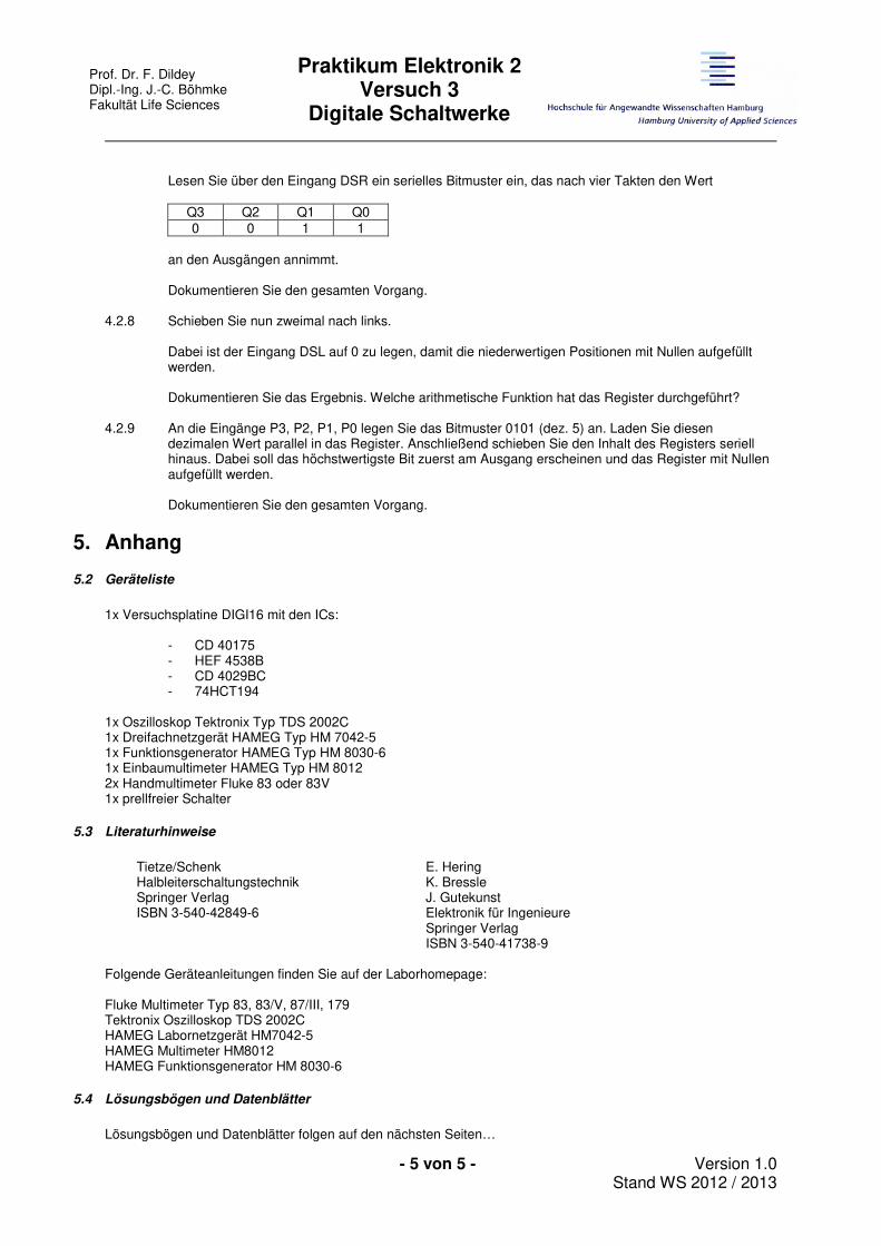
Lesen Sie über den Eingang DSR ein serielles Bitmuster ein, das nach vier Takten den Wert
Q3 Q2 Q1 Q0 0 0 1 1
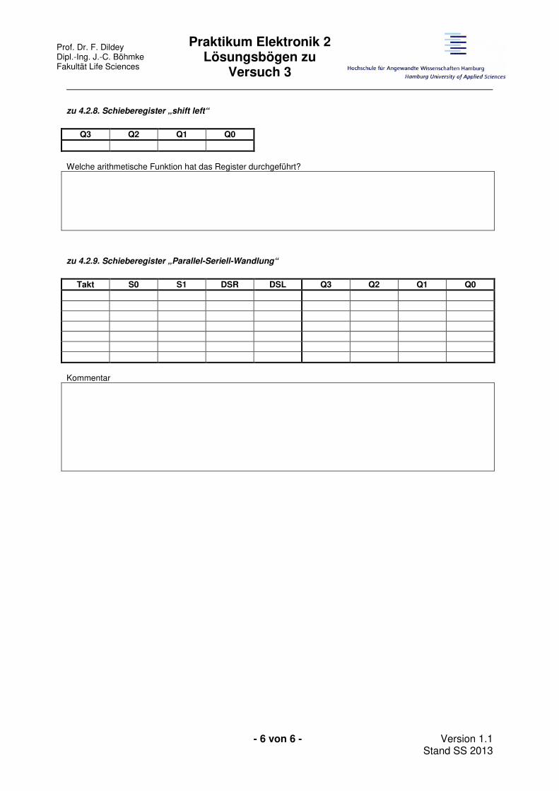
an den Ausgängen annimmt. Dokumentieren Sie den gesamten Vorgang. 4.2.8 Schieben Sie nun zweimal nach links.
Dabei ist der Eingang DSL auf 0 zu legen, damit die niederwertigen Positionen mit Nullen aufgefüllt werden. Dokumentieren Sie das Ergebnis. Welche arithmetische Funktion hat das Register durchgeführt?
4.2.9 An die Eingänge P3, P2, P1, P0 legen Sie das Bitmuster 0101 (dez. 5) an. Laden Sie diesen
dezimalen Wert parallel in das Register. Anschließend schieben Sie den Inhalt des Registers seriell hinaus. Dabei soll das höchstwertigste Bit zuerst am Ausgang erscheinen und das Register mit Nullen aufgefüllt werden.
Dokumentieren Sie den gesamten Vorgang.
5. Anhang
5.2 Geräteliste
1x Versuchsplatine DIGI16 mit den ICs:
- CD 40175 - HEF 4538B - CD 4029BC - 74HCT194
1x Oszilloskop Tektronix Typ TDS 2002C 1x Dreifachnetzgerät HAMEG Typ HM 7042-5 1x Funktionsgenerator HAMEG Typ HM 8030-6 1x Einbaumultimeter HAMEG Typ HM 8012 2x Handmultimeter Fluke 83 oder 83V 1x prellfreier Schalter
5.3 Literaturhinweise
Tietze/Schenk Halbleiterschaltungstechnik Springer Verlag ISBN 3-540-42849-6
E. Hering K. Bressle J. Gutekunst Elektronik für Ingenieure Springer Verlag ISBN 3-540-41738-9
Folgende Geräteanleitungen finden Sie auf der Laborhomepage: Fluke Multimeter Typ 83, 83/V, 87/III, 179 Tektronix Oszilloskop TDS 2002C HAMEG Labornetzgerät HM7042-5 HAMEG Multimeter HM8012 HAMEG Funktionsgenerator HM 8030-6
5.4 Lösungsbögen und Datenblätter
Lösungsbögen und Datenblätter folgen auf den nächsten Seiten…

Prof. Dr. F. Dildey Dipl.-Ing. J.-C. Böhmke Fakultät Life Sciences
Praktikum Elektronik 2 Lösungsbögen zu
Versuch 3
- 1 von 6 - Version 1.1 Stand SS 2013
1. Vorbereitung
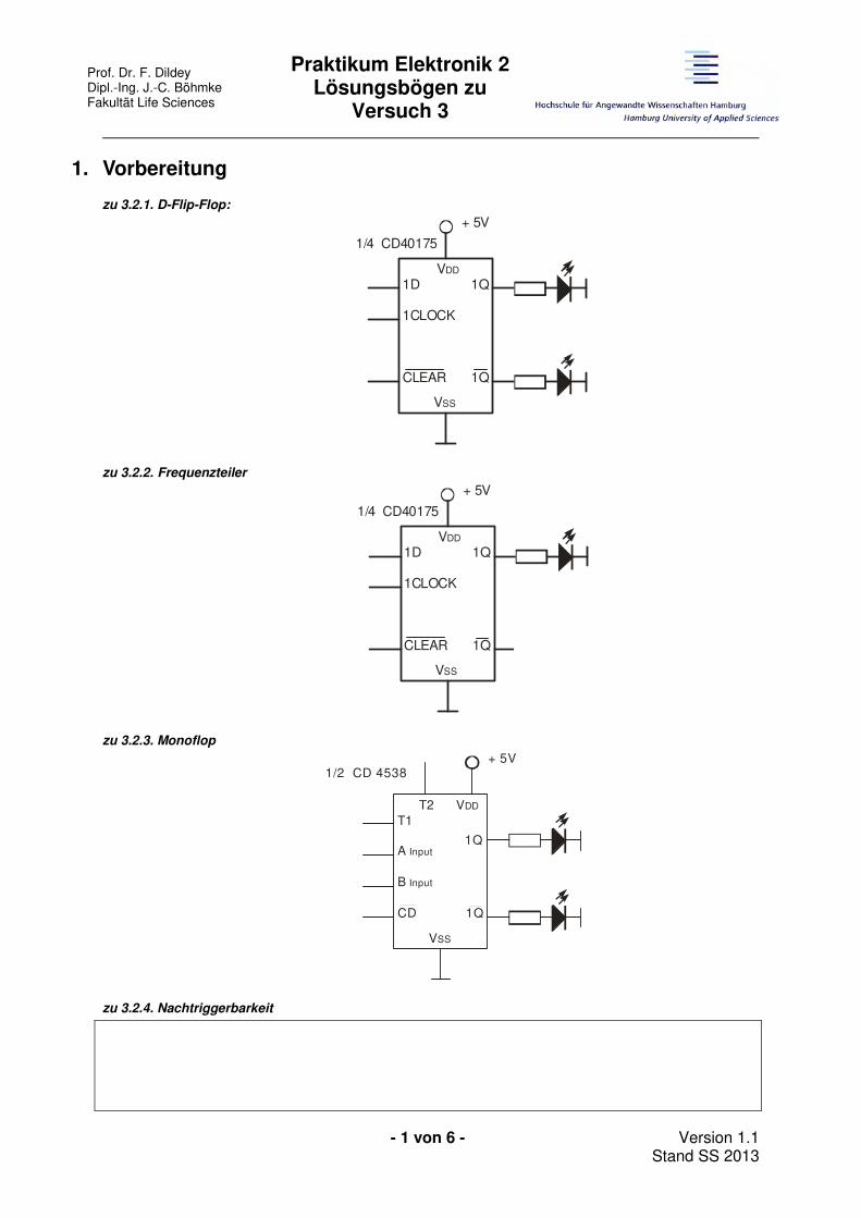
zu 3.2.1. D-Flip-Flop:
1D
1CLOCK
CLEAR
VSS
VDD
1Q
1Q
+ 5V
1/4 CD40175
zu 3.2.2. Frequenzteiler
1D
1CLOCK
CLEAR
VSS
VDD
1Q
1Q
+ 5V
1/4 CD40175
zu 3.2.3. Monoflop
T1
CD
VSS
VDD
1Q
1Q
+ 5V1/2 CD 4538
T2
B Input
A Input
zu 3.2.4. Nachtriggerbarkeit
Prof. Dr. F. Dildey Dipl.-Ing. J.-C. Böhmke Fakultät Life Sciences
Praktikum Elektronik 2 Lösungsbögen zu
Versuch 3
- 2 von 6 - Version 1.1 Stand SS 2013
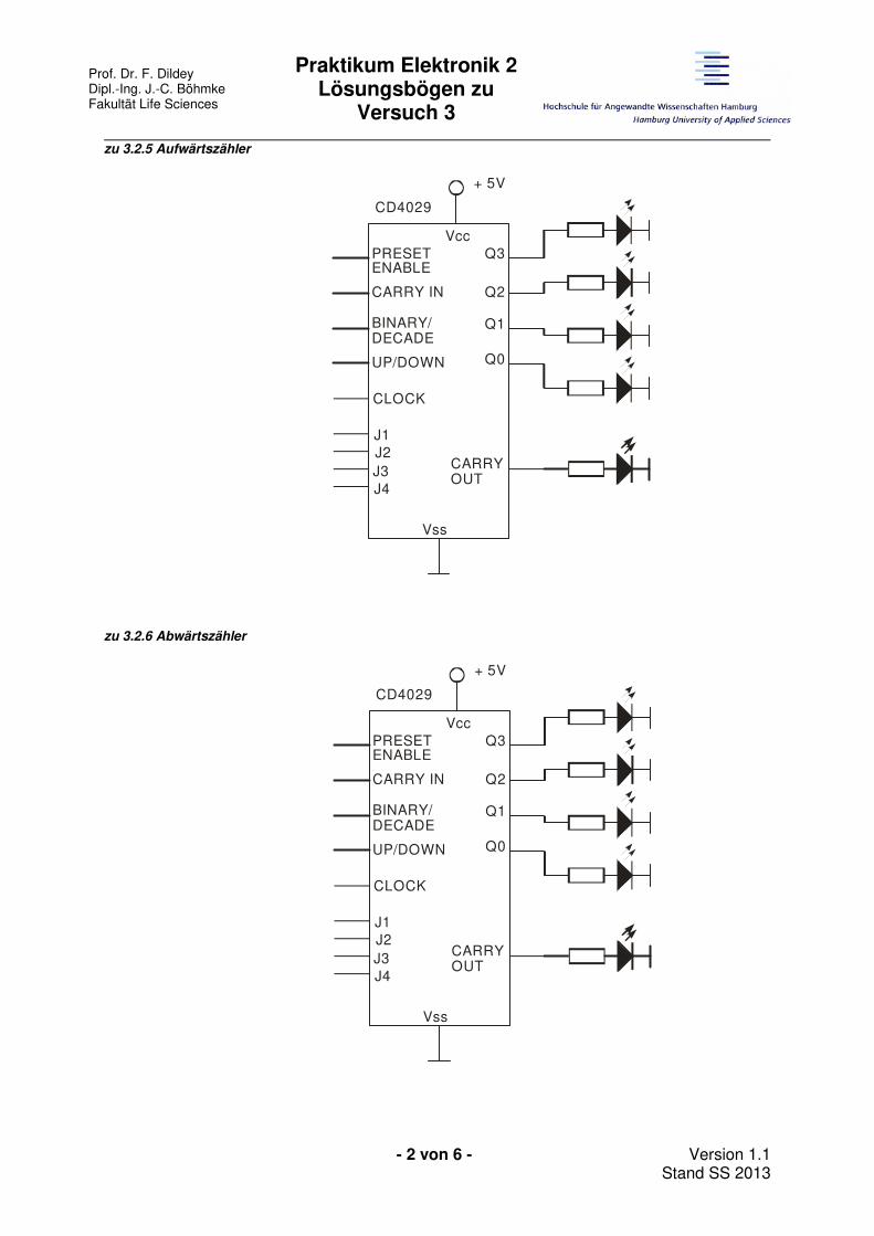
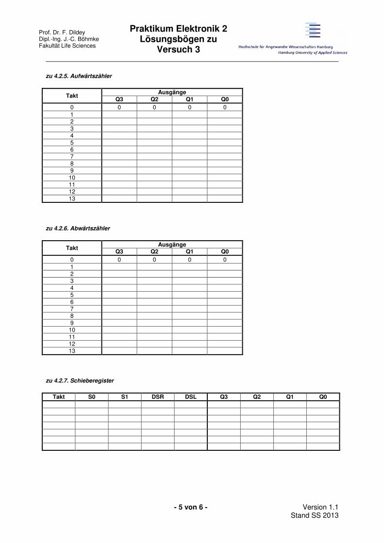
zu 3.2.5 Aufwärtszähler
PRESET ENABLE
CARRY IN
BINARY/DECADE
UP/DOWN
CLOCK
J1
J2
J3
J4
CARRY OUT
Vss
Vcc
Q3
Q2
Q1
Q0
+ 5V
CD4029
zu 3.2.6 Abwärtszähler
PRESET ENABLE
CARRY IN
BINARY/DECADE
UP/DOWN
CLOCK
J1
J2
J3
J4
CARRY OUT
Vss
Vcc
Q3
Q2
Q1
Q0
+ 5V
CD4029
Prof. Dr. F. Dildey Dipl.-Ing. J.-C. Böhmke Fakultät Life Sciences
Praktikum Elektronik 2 Lösungsbögen zu
Versuch 3
- 3 von 6 - Version 1.1 Stand SS 2013
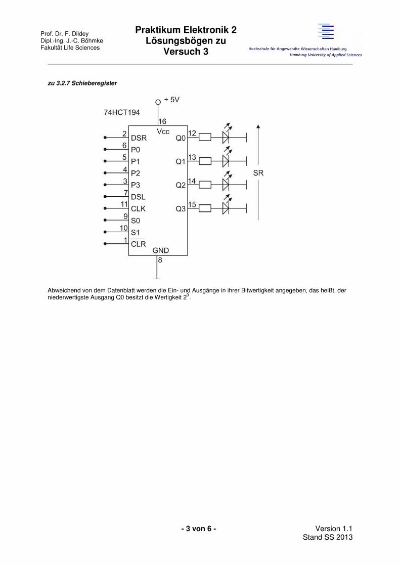
zu 3.2.7 Schieberegister
Abweichend von dem Datenblatt werden die Ein- und Ausgänge in ihrer Bitwertigkeit angegeben, das heißt, der niederwertigste Ausgang Q0 besitzt die Wertigkeit 2
0 .
Prof. Dr. F. Dildey Dipl.-Ing. J.-C. Böhmke Fakultät Life Sciences
Praktikum Elektronik 2 Lösungsbögen zu
Versuch 3
- 4 von 6 - Version 1.1 Stand SS 2013
2. Versuchsdurchführung
zu 4.2.1. D-Flip-Flop
Eingänge Ausgänge
CLEAR CLOCK D 1−Q
1−Q Q Q
0 X X
1 X X
1 ↓ 1
1 ↑ 1
1 ↓ 0
1 ↑ 0
bedeutet Signal vor der Zustandsänderung
zu 4.2.2. Frequenzteiler
siehe Ausdruck Nr. Kommentar
zu 4.2.3. Monoflop
siehe Ausdruck Nr. Kommentar
zu 4.2.4. Aufwärtszähler
siehe Ausdruck Nr. Kommentar
1Q−
Prof. Dr. F. Dildey Dipl.-Ing. J.-C. Böhmke Fakultät Life Sciences
Praktikum Elektronik 2 Lösungsbögen zu
Versuch 3
- 5 von 6 - Version 1.1 Stand SS 2013
zu 4.2.5. Aufwärtszähler
Takt Ausgänge
Q3 Q2 Q1 Q0
0 0 0 0 0
1
2
3
4
5
6
7
8
9
10
11
12
13
zu 4.2.6. Abwärtszähler
Takt Ausgänge
Q3 Q2 Q1 Q0
0 0 0 0 0
1
2
3
4
5
6
7
8
9
10
11
12
13
zu 4.2.7. Schieberegister
Takt S0 S1 DSR DSL Q3 Q2 Q1 Q0
Prof. Dr. F. Dildey Dipl.-Ing. J.-C. Böhmke Fakultät Life Sciences
Praktikum Elektronik 2 Lösungsbögen zu
Versuch 3
- 6 von 6 - Version 1.1 Stand SS 2013
zu 4.2.8. Schieberegister „shift left“
Q3 Q2 Q1 Q0
Welche arithmetische Funktion hat das Register durchgeführt?
zu 4.2.9. Schieberegister „Parallel-Seriell-Wandlung“
Takt S0 S1 DSR DSL Q3 Q2 Q1 Q0
Kommentar
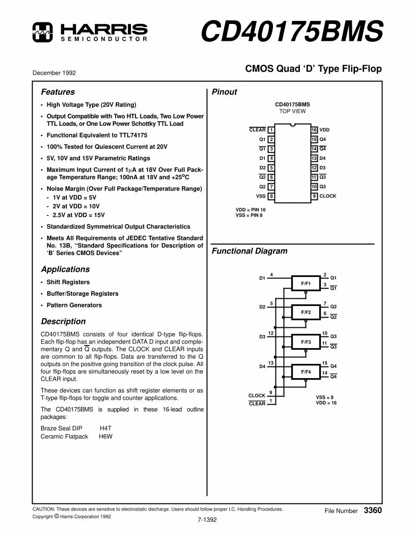
CAUTION: These devices are sensitive to electrostatic discharge. Users should follow proper I.C. Handling Procedures.
Copyright © Harris Corporation 19927-1392
S E M I C O N D U C T O R CD40175BMSCMOS Quad ‘D’ Type Flip-Flop
Features
• High Voltage Type (20V Rating)
• Output Compatible with Two HTL Loads, Two Low Power
TTL Loads, or One Low Power Schottky TTL Load
• Functional Equivalent to TTL74175
• 100% Tested for Quiescent Current at 20V
• 5V, 10V and 15V Parametric Ratings
• Maximum Input Current of 1µA at 18V Over Full Pack-
age Temperature Range; 100nA at 18V and +25oC
• Noise Margin (Over Full Package/Temperature Range)
- 1V at VDD = 5V
- 2V at VDD = 10V
- 2.5V at VDD = 15V
• Standardized Symmetrical Output Characteristics
• Meets All Requirements of JEDEC Tentative Standard
No. 13B, “Standard Specifications for Description of
‘B’ Series CMOS Devices”
Applications
• Shift Registers
• Buffer/Storage Registers
• Pattern Generators
Description
CD40175BMS consists of four identical D-type flip-flops.
Each flip-flop has an independent DATA D input and comple-
mentary Q and Q outputs. The CLOCK and CLEAR inputs
are common to all flip-flops. Data are transferred to the Q
outputs on the positive going transition of the clock pulse. All
four flip-flops are simultaneously reset by a low level on the
CLEAR input.
These devices can function as shift register elements or as
T-type flip-flops for toggle and counter applications.
The CD40175BMS is supplied in these 16-lead outline
packages:
Braze Seal DIP H4T
Ceramic Flatpack H6W
December 1992
File Number 3360
Pinout
CD40175BMS
TOP VIEW
Functional Diagram
14
15
16
9
13
12
11
10
1
2
3
4
5
7
6
8
CLEAR
Q1
Q1
D1
D2
Q2
VSS
Q2
VDD
Q4
D4
D3
Q3
Q3
CLOCK
Q4
VDD = PIN 16VSS = PIN 8
F/F1
4D1
2
3
Q1
Q1
F/F2
5D2
7
6
Q2
Q2
F/F3
12D3
10
11
Q3
Q3
F/F4
13D4
15
14
Q4
Q4
9CLOCK
1CLEAR
VSS = 8VDD = 16
7-1393
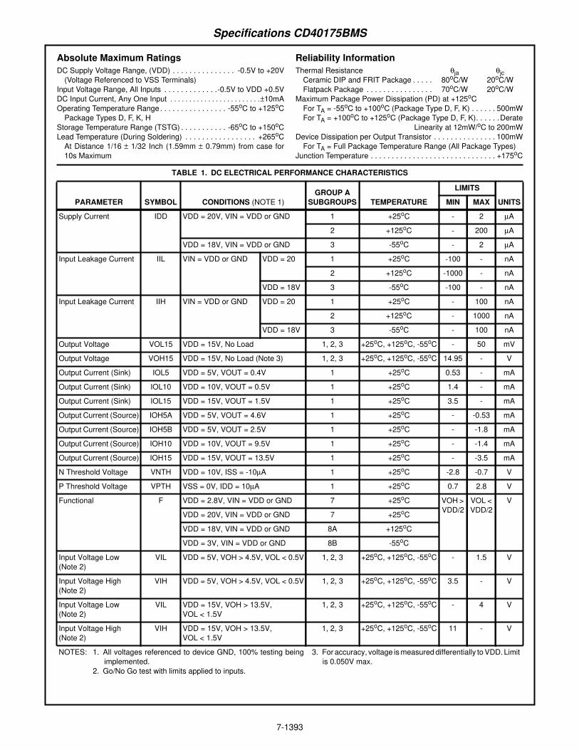
Specifications CD40175BMS
Absolute Maximum Ratings Reliability Information
DC Supply Voltage Range, (VDD) . . . . . . . . . . . . . . . -0.5V to +20V
(Voltage Referenced to VSS Terminals)
Input Voltage Range, All Inputs . . . . . . . . . . . . .-0.5V to VDD +0.5V
DC Input Current, Any One Input . . . . . . . . . . . . . . . . . . . . . . . .±10mA
Operating Temperature Range. . . . . . . . . . . . . . . . -55oC to +125oC
Package Types D, F, K, H
Storage Temperature Range (TSTG) . . . . . . . . . . . -65oC to +150oC
Lead Temperature (During Soldering) . . . . . . . . . . . . . . . . . +265oC
At Distance 1/16 ± 1/32 Inch (1.59mm ± 0.79mm) from case for
10s Maximum
Thermal Resistance θja θjc
Ceramic DIP and FRIT Package . . . . . 80oC/W 20oC/W
Flatpack Package . . . . . . . . . . . . . . . . 70oC/W 20oC/W
Maximum Package Power Dissipation (PD) at +125oC
For TA = -55oC to +100oC (Package Type D, F, K) . . . . . . 500mW
For TA = +100oC to +125oC (Package Type D, F, K). . . . . .Derate
Linearity at 12mW/oC to 200mW
Device Dissipation per Output Transistor . . . . . . . . . . . . . . . 100mW
For TA = Full Package Temperature Range (All Package Types)
Junction Temperature . . . . . . . . . . . . . . . . . . . . . . . . . . . . . . +175oC
TABLE 1. DC ELECTRICAL PERFORMANCE CHARACTERISTICS
PARAMETER SYMBOL CONDITIONS (NOTE 1)
GROUP A
SUBGROUPS TEMPERATURE
LIMITS
UNITSMIN MAX
Supply Current IDD VDD = 20V, VIN = VDD or GND 1 +25oC - 2 µA
2 +125oC - 200 µA
VDD = 18V, VIN = VDD or GND 3 -55oC - 2 µA
Input Leakage Current IIL VIN = VDD or GND VDD = 20 1 +25oC -100 - nA
2 +125oC -1000 - nA
VDD = 18V 3 -55oC -100 - nA
Input Leakage Current IIH VIN = VDD or GND VDD = 20 1 +25oC - 100 nA
2 +125oC - 1000 nA
VDD = 18V 3 -55oC - 100 nA
Output Voltage VOL15 VDD = 15V, No Load 1, 2, 3 +25oC, +125oC, -55oC - 50 mV
Output Voltage VOH15 VDD = 15V, No Load (Note 3) 1, 2, 3 +25oC, +125oC, -55oC 14.95 - V
Output Current (Sink) IOL5 VDD = 5V, VOUT = 0.4V 1 +25oC 0.53 - mA
Output Current (Sink) IOL10 VDD = 10V, VOUT = 0.5V 1 +25oC 1.4 - mA
Output Current (Sink) IOL15 VDD = 15V, VOUT = 1.5V 1 +25oC 3.5 - mA
Output Current (Source) IOH5A VDD = 5V, VOUT = 4.6V 1 +25oC - -0.53 mA
Output Current (Source) IOH5B VDD = 5V, VOUT = 2.5V 1 +25oC - -1.8 mA
Output Current (Source) IOH10 VDD = 10V, VOUT = 9.5V 1 +25oC - -1.4 mA
Output Current (Source) IOH15 VDD = 15V, VOUT = 13.5V 1 +25oC - -3.5 mA
N Threshold Voltage VNTH VDD = 10V, ISS = -10µA 1 +25oC -2.8 -0.7 V
P Threshold Voltage VPTH VSS = 0V, IDD = 10µA 1 +25oC 0.7 2.8 V
Functional F VDD = 2.8V, VIN = VDD or GND 7 +25oC VOH >
VDD/2
VOL <
VDD/2
V
VDD = 20V, VIN = VDD or GND 7 +25oC
VDD = 18V, VIN = VDD or GND 8A +125oC
VDD = 3V, VIN = VDD or GND 8B -55oC
Input Voltage Low
(Note 2)
VIL VDD = 5V, VOH > 4.5V, VOL < 0.5V 1, 2, 3 +25oC, +125oC, -55oC - 1.5 V
Input Voltage High
(Note 2)
VIH VDD = 5V, VOH > 4.5V, VOL < 0.5V 1, 2, 3 +25oC, +125oC, -55oC 3.5 - V
Input Voltage Low
(Note 2)
VIL VDD = 15V, VOH > 13.5V,
VOL < 1.5V
1, 2, 3 +25oC, +125oC, -55oC - 4 V
Input Voltage High
(Note 2)
VIH VDD = 15V, VOH > 13.5V,
VOL < 1.5V
1, 2, 3 +25oC, +125oC, -55oC 11 - V
NOTES: 1. All voltages referenced to device GND, 100% testing being
implemented.
2. Go/No Go test with limits applied to inputs.
3. For accuracy, voltage is measured differentially to VDD. Limit
is 0.050V max.
7-1394
Specifications CD40175BMS
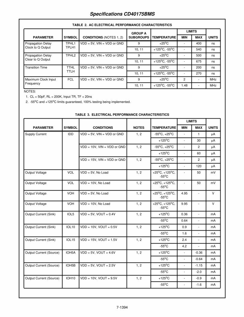
TABLE 2. AC ELECTRICAL PERFORMANCE CHARACTERISTICS
PARAMETER SYMBOL CONDITIONS (NOTES 1, 2)
GROUP A
SUBGROUPS TEMPERATURE
LIMITS
UNITSMIN MAX
Propagation Delay
Clock to Q Output
TPHL1
TPLH1
VDD = 5V, VIN = VDD or GND 9 +25oC - 400 ns
10, 11 +125oC, -55oC - 540 ns
Propagation Delay
Clear to Q Output
TPHL2 VDD = 5V, VIN = VDD or GND 9 +25oC - 500 ns
10, 11 +125oC, -55oC - 675 ns
Transition Time TTHL
TTLH
VDD = 5V, VIN = VDD or GND 9 +25oC - 200 ns
10, 11 +125oC, -55oC - 270 ns
Maximum Clock Input
Frequency
FCL VDD = 5V, VIN = VDD or GND 9 +25oC 2 - MHz
10, 11 +125oC, -55oC 1.48 - MHz
NOTES:
1. CL = 50pF, RL = 200K, Input TR, TF < 20ns
2. -55oC and +125oC limits guaranteed, 100% testing being implemented.
TABLE 3. ELECTRICAL PERFORMANCE CHARACTERISTICS
PARAMETER SYMBOL CONDITIONS NOTES TEMPERATURE
LIMITS
UNITSMIN MAX
Supply Current IDD VDD = 5V, VIN = VDD or GND 1, 2 -55oC, +25oC - 1 µA
+125oC - 30 µA
VDD = 10V, VIN = VDD or GND 1, 2 -55oC, +25oC - 2 µA
+125oC - 60 µA
VDD = 15V, VIN = VDD or GND 1, 2 -55oC, +25oC - 2 µA
+125oC - 120 µA
Output Voltage VOL VDD = 5V, No Load 1, 2 +25oC, +125oC,
-55oC
- 50 mV
Output Voltage VOL VDD = 10V, No Load 1, 2 +25oC, +125oC,
-55oC
- 50 mV
Output Voltage VOH VDD = 5V, No Load 1, 2 +25oC, +125oC,
-55oC
4.95 - V
Output Voltage VOH VDD = 10V, No Load 1, 2 +25oC, +125oC,
-55oC
9.95 - V
Output Current (Sink) IOL5 VDD = 5V, VOUT = 0.4V 1, 2 +125oC 0.36 - mA
-55oC 0.64 - mA
Output Current (Sink) IOL10 VDD = 10V, VOUT = 0.5V 1, 2 +125oC 0.9 - mA
-55oC 1.6 - mA
Output Current (Sink) IOL15 VDD = 15V, VOUT = 1.5V 1, 2 +125oC 2.4 - mA
-55oC 4.2 - mA
Output Current (Source) IOH5A VDD = 5V, VOUT = 4.6V 1, 2 +125oC - -0.36 mA
-55oC - -0.64 mA
Output Current (Source) IOH5B VDD = 5V, VOUT = 2.5V 1, 2 +125oC - -1.15 mA
-55oC - -2.0 mA
Output Current (Source) IOH10 VDD = 10V, VOUT = 9.5V 1, 2 +125oC - -0.9 mA
-55oC - -1.6 mA
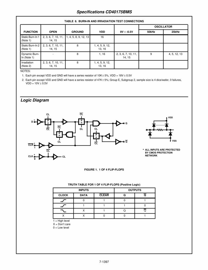
7-1397
Specifications CD40175BMS
TABLE 8. BURN-IN AND IRRADIATION TEST CONNECTIONS
FUNCTION OPEN GROUND VDD 9V ± -0.5V
OSCILLATOR
50kHz 25kHz
Static Burn-In 1
(Note 1)
2, 3, 6, 7, 10, 11,
14, 15
1, 4, 5, 8, 9, 12, 13 16
Static Burn-In 2
(Note 1)
2, 3, 6, 7, 10, 11,
14, 15
8 1, 4, 5, 9, 12,
13, 16
Dynamic Burn-
In (Note 1)
- 8 1, 16 2, 3, 6, 7, 10, 11,
14, 15
9 4, 5, 12, 13
Irradiation
(Note 2)
2, 3, 6, 7, 10, 11,
14, 15
8 1, 4, 5, 9, 12,
13, 16
NOTES:
1. Each pin except VDD and GND will have a series resistor of 10K ± 5%, VDD = 18V ± 0.5V
2. Each pin except VDD and GND will have a series resistor of 47K ± 5%; Group E, Subgroup 2, sample size is 4 dice/wafer, 0 failures,
VDD = 10V ± 0.5V
Logic Diagram
FIGURE 1. 1 OF 4 FLIP-FLOPS
TRUTH TABLE FOR 1 OF 4 FLIP-FLOPS (Positive Logic)
INPUTS OUTPUTS
CLOCK DATA CLEAR Q Q
0 1 0 1
1 1 1 0
X 1 Q Q
X X 0 0 1
1 = High level
X = Don’t care
0 = Low level
CL
CL
CLR *1
CLK *9
CL
CL
CL
CL
pn
pn
CL
CL
* ALL INPUTS ARE PROTECTED
BY CMOS PROTECTION
NETWORK
VDD
VSS
CL
CL
pnD *
Q
Q
pn
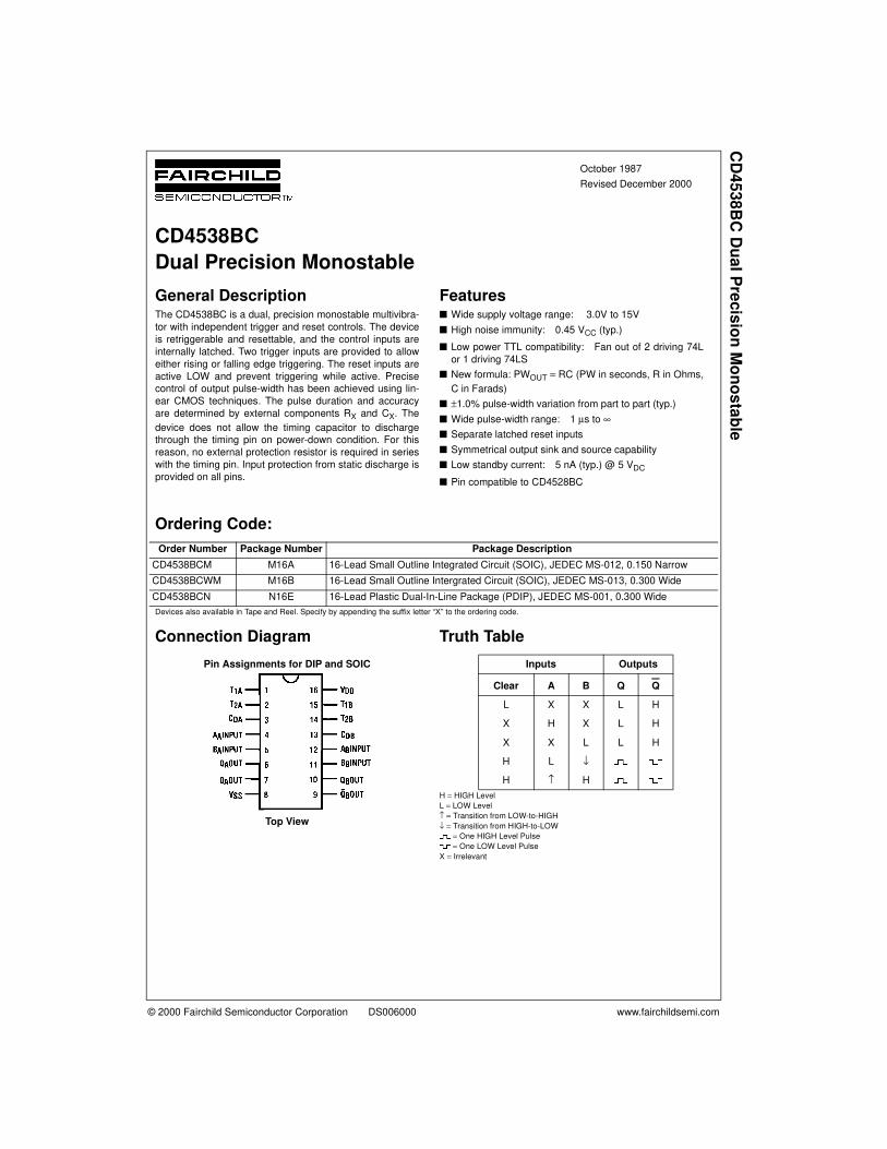
© 2000 Fairchild Semiconductor Corporation DS006000 www.fairchildsemi.com
October 1987
Revised December 2000
CD
45
38
BC
Du
al P
recis
ion
Mo
no
sta
ble
CD4538BC
Dual Precision Monostable
General DescriptionThe CD4538BC is a dual, precision monostable multivibra-
tor with independent trigger and reset controls. The device
is retriggerable and resettable, and the control inputs are
internally latched. Two trigger inputs are provided to allow
either rising or falling edge triggering. The reset inputs are
active LOW and prevent triggering while active. Precise
control of output pulse-width has been achieved using lin-
ear CMOS techniques. The pulse duration and accuracy
are determined by external components RX and CX. The
device does not allow the timing capacitor to discharge
through the timing pin on power-down condition. For this
reason, no external protection resistor is required in series
with the timing pin. Input protection from static discharge is
provided on all pins.
Features Wide supply voltage range: 3.0V to 15V
High noise immunity: 0.45 VCC (typ.)
Low power TTL compatibility: Fan out of 2 driving 74L
or 1 driving 74LS
New formula: PWOUT = RC (PW in seconds, R in Ohms,
C in Farads)
±1.0% pulse-width variation from part to part (typ.)
Wide pulse-width range: 1 µs to ∞
Separate latched reset inputs
Symmetrical output sink and source capability
Low standby current: 5 nA (typ.) @ 5 VDC
Pin compatible to CD4528BC
Ordering Code:
Devices also available in Tape and Reel. Specify by appending the suffix letter “X” to the ordering code.
Connection Diagram
Pin Assignments for DIP and SOIC
Top View
Truth Table
H = HIGH Level
L = LOW Level
↑ = Transition from LOW-to-HIGH
↓ = Transition from HIGH-to-LOW
= One HIGH Level Pulse
= One LOW Level Pulse
X = Irrelevant
Order Number Package Number Package Description
CD4538BCM M16A 16-Lead Small Outline Integrated Circuit (SOIC), JEDEC MS-012, 0.150 Narrow
CD4538BCWM M16B 16-Lead Small Outline Intergrated Circuit (SOIC), JEDEC MS-013, 0.300 Wide
CD4538BCN N16E 16-Lead Plastic Dual-In-Line Package (PDIP), JEDEC MS-001, 0.300 Wide
Inputs Outputs
Clear A B Q Q
L X X L H
X H X L H
X X L L H
H L ↓
H ↑ H
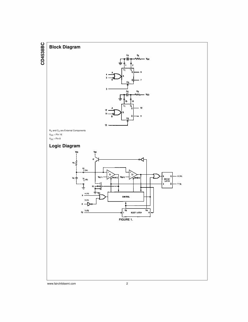
www.fairchildsemi.com 2
CD
453
8B
CBlock Diagram
RX and CX are External Components
VDD = Pin 16
VSS = Pin 8
Logic Diagram
FIGURE 1.
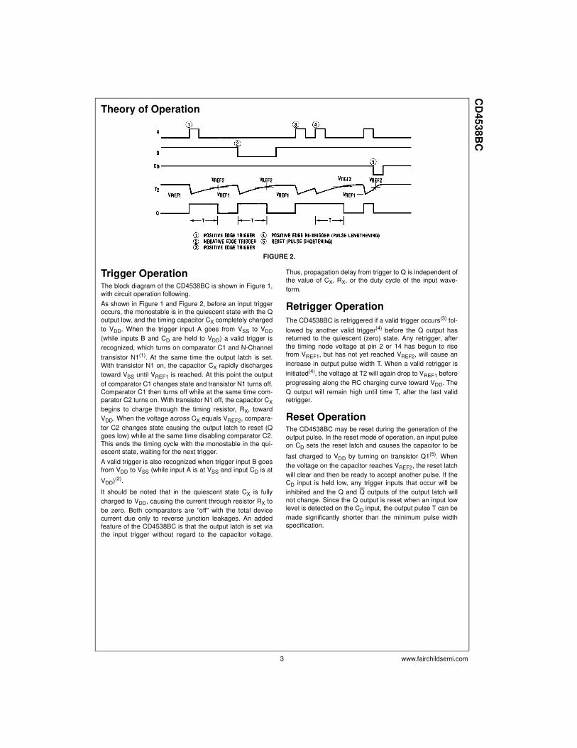
3 www.fairchildsemi.com
CD
45
38
BC
Theory of Operation
FIGURE 2.
Trigger OperationThe block diagram of the CD4538BC is shown in Figure 1,
with circuit operation following.
As shown in Figure 1 and Figure 2, before an input trigger
occurs, the monostable is in the quiescent state with the Q
output low, and the timing capacitor CX completely charged
to VDD. When the trigger input A goes from VSS to VDD
(while inputs B and CD are held to VDD) a valid trigger is
recognized, which turns on comparator C1 and N-Channel
transistor N1(1). At the same time the output latch is set.
With transistor N1 on, the capacitor CX rapidly discharges
toward VSS until VREF1 is reached. At this point the output
of comparator C1 changes state and transistor N1 turns off.
Comparator C1 then turns off while at the same time com-
parator C2 turns on. With transistor N1 off, the capacitor CX
begins to charge through the timing resistor, RX, toward
VDD. When the voltage across CX equals VREF2, compara-
tor C2 changes state causing the output latch to reset (Q
goes low) while at the same time disabling comparator C2.
This ends the timing cycle with the monostable in the qui-
escent state, waiting for the next trigger.
A valid trigger is also recognized when trigger input B goes
from VDD to VSS (while input A is at VSS and input CD is at
VDD)(2).
It should be noted that in the quiescent state CX is fully
charged to VDD, causing the current through resistor RX to
be zero. Both comparators are “off” with the total device
current due only to reverse junction leakages. An added
feature of the CD4538BC is that the output latch is set via
the input trigger without regard to the capacitor voltage.
Thus, propagation delay from trigger to Q is independent of
the value of CX, RX, or the duty cycle of the input wave-
form.
Retrigger Operation
The CD4538BC is retriggered if a valid trigger occurs(3) fol-
lowed by another valid trigger(4) before the Q output has
returned to the quiescent (zero) state. Any retrigger, after
the timing node voltage at pin 2 or 14 has begun to rise
from VREF1, but has not yet reached VREF2, will cause an
increase in output pulse width T. When a valid retrigger is
initiated(4), the voltage at T2 will again drop to VREF1 before
progressing along the RC charging curve toward VDD. The
Q output will remain high until time T, after the last valid
retrigger.
Reset OperationThe CD4538BC may be reset during the generation of the
output pulse. In the reset mode of operation, an input pulse
on CD sets the reset latch and causes the capacitor to be
fast charged to VDD by turning on transistor Q1(5). When
the voltage on the capacitor reaches VREF2, the reset latch
will clear and then be ready to accept another pulse. If the
CD input is held low, any trigger inputs that occur will be
inhibited and the Q and Q outputs of the output latch will
not change. Since the Q output is reset when an input low
level is detected on the CD input, the output pulse T can be
made significantly shorter than the minimum pulse width
specification.
www.fairchildsemi.com 4
CD
453
8B
C
FIGURE 3. Retriggerable Monostables Circuitry FIGURE 4. Non-Retriggerable Monostables Circuitry
FIGURE 5. Connection of Unused Sections
5 www.fairchildsemi.com
CD
45
38
BC
Absolute Maximum Ratings(Note 1)
(Note 2)
Recommended OperatingConditions (Note 2)
Note 1: “Absolute Maximum Ratings” are those values beyond which the
safety of the device cannot be guaranteed, they are not meant to imply that
the devices should be operated at these limits. The tables of “Recom-
mended Operating Conditions” and “Electrical Characteristics” provide con-
ditions for actual device operation.
Note 2: VSS = 0V unless otherwise specified.
DC Electrical Characteristics (Note 2)
Note 3: IOH and IOL are tested one output at a time.
DC Supply Voltage (VDD) −0.5 to +18 VDC
Input Voltage (VIN) −0.5V to VDD + 0.5 VDC
Storage Temperature Range (TS) −65°C to +150°C
Power Dissipation (PD)
Dual-In-Line 700 mW
Small Outline 500 mW
Lead Temperature (TL)
(Soldering, 10 seconds) 260°C
DC Supply Voltage (VDD) 3 to 15 VDC
Input Voltage (VIN) 0 to VDD VDC
Operating Temperature Range (TA) −40°C to +85°C
Symbol Parameter Conditions−40°C +25°C +85°C
UnitsMin Max Min Typ Max Min Max
IDD Quiescent VDD = 5V VIH = VDD 20 0.005 20 150 µA
Device Current VDD = 10V VIL = VSS 40 0.010 40 300 µA
VDD = 15V All Outputs Open 80 0.015 80 600 µA
VOL LOW Level VDD = 5V |IO| < 1 µA 0.05 0 0.05 0.05 V
Output Voltage VDD = 10V VIH = VDD, VIL = VSS 0.05 0 0.05 0.05 V
VDD = 15V 0.05 0 0.05 0.05 V
VOH HIGH Level VDD = 5V |IO| < 1 µA 4.95 4.95 5 4.95 V
Output Voltage VDD = 10V VIH = VDD, VIL = VSS 9.95 9.95 10 9.95 V
VDD = 15V 14.95 14.95 15 14.95 V
VIL LOW Level |IO| < 1 µA
Input Voltage VDD = 5V, VO = 0.5V or 4.5V 1.5 2.25 1.5 1.5 V
VDD = 10V, VO = 1.0V or 9.0V 3.0 4.50 3.0 3.0 V
VDD = 15V, VO = 1.5V or 13.5V 4.0 6.75 4.0 4.0 V
VIH HIGH Level |IO| < 1 µA
Input Voltage VDD = 5V, VO = 0.5V or 4.5V 3.5 3.5 2.75 3.5 V
VDD = 10V, VO = 1.0V or 9.0V 7.0 7.0 5.50 7.0 V
VDD = 15V, VO = 1.5V or 13.5V 11.0 11.0 8.25 11.0 V
IOL LOW Level VDD = 5V, VO = 0.4V VIH = VDD 0.52 0.44 0.88 0.36 mA
Output Current VDD = 10V, VO = 0.5V VIL = VSS 1.3 1.1 2.25 0.9 mA
(Note 3) VD = 15V, VO = 1.5V 3.6 3.0 8.8 2.4 mA
IOH HIGH Level VDD = 5V, VO = 4.6V −0.52 −0.44 −0.88 −0.36 mA
Output Current VDD = 10V, VO = 9.5V VIL = VSS −1.3 −1.1 −2.25 −0.9 mA
(Note 3) VD = 15V, VO = 13.5V −3.6 −3.0 −8.8 −2.4 mA
IIN Input Current, VDD = 15V, VIN = 0V or 15V ±0.02 ±10−5 ±0.05 ±0.5 µA
Pin 2 or 14
IIN Input Current VDD = 15V, VIN = 0V or 15V ±0.3 ±10−5 ±0.3 ±1.0 µA
Other Inputs
www.fairchildsemi.com 6
CD
453
8B
CAC Electrical Characteristics (Note 4)
TA = 25°C, CL = 50 pF, and tr = tf = 20 ns unless otherwise specified
Note 4: AC parameters are guaranteed by DC correlated testing.
Note 5: The maximum usable resistance RX is a function of the leakage of the Capacitor CX, leakage of the CD4538BC, and leakage due to board layout,
surface resistance, etc.
Symbol Parameter Conditions Min Typ Max Units
tTLH, tTHL Output Transition Time VDD = 5V 100 200 ns
VDD = 10V 50 100 ns
VDD = 15V 40 80 ns
tPLH, tPHL Propagation Delay Time Trigger Operation—
A or B to Q or Q
VDD = 5V 300 600 ns
VDD = 10V 150 300 ns
VDD = 15V 100 220 ns
Reset Operation—
CD to Q or Q
VDD = 5V 250 500 ns
VDD = 10V 125 250 ns
VDD = 15V 95 190 ns
tWL, tWH Minimum Input Pulse Width VDD = 5V 35 70 ns
A, B, or CD VDD = 10V 30 60 ns
VDD = 15V 25 50 ns
tRR Minimum Retrigger Time VDD = 5V 0 ns
VDD = 10V 0 0 ns
VDD = 15V 0 ns
CIN Input Capacitance Pin 2 or 14 10 pF
Other Inputs 5 7.5 pF
PWOUT Output Pulse Width (Q or Q) RX = 100 kΩ VDD = 5V 208 226 244 µs
(Note: For Typical Distribution, CX = 0.002 µF VDD = 10V 211 230 248 µs
see Figure 6) VDD = 15V 216 235 254 µs
RX = 100 kΩ VDD = 5V 8.83 9.60 10.37 ms
CX = 0.1 µF VDD = 10V 9.02 9.80 10.59 ms
VDD = 15V 9.20 10.00 10.80 ms
RX = 100 kΩ VDD = 5V 0.87 0.95 1.03 s
CX = 10.0 µF VDD = 10V 0.89 0.97 1.05 s
VDD = 15V 0.91 0.99 1.07 s
Pulse Width Match between RX = 100 kΩ VDD = 5V ±1 %
Circuits in the Same Package CX = 0.1 µF VDD = 10V ±1 %
CX = 0.1 µF, RX = 100 kΩ VDD = 15V ±1 %
Operating Conditions
RX External Timing Resistance 5.0 (Note 5) kΩ
CX External Timing Capacitance 0 No Limit pF
7 www.fairchildsemi.com
CD
45
38
BC
Typical Applications
FIGURE 6. Typical Normalized Distribution of Units
for Output Pulse Width
FIGURE 7. Typical Pulse Width Variation as a
Function of Supply Voltage VDD
FIGURE 8. Typical Total Supply Current Versus
Output Duty Cycle, RX = 100 kΩ, CL = 50 pF,
CX = 100 pF, One Monostable Switching Only
FIGURE 9. Typical Pulse Width Error
Versus Temperature
FIGURE 10. Typical Pulse Width Error
Versus Temperature
FIGURE 11. Typical Pulse Width Versus
Timing RC Product
October 1987
Revised January 1999
CD
40
29
BC
Pre
setta
ble
Bin
ary
/Dec
ad
e U
p/D
ow
n C
ou
nte
r
© 1999 Fairchild Semiconductor Corporation DS005960.prf www.fairchildsemi.com
CD4029BC
Presettable Binary/Decade Up/Down Counter
General DescriptionThe CD4029BC is a presettable up/down counter which
counts in either binary or decade mode depending on the
voltage level applied at binary/decade input. When binary/
decade is at logical “1”, the counter counts in binary, other-
wise it counts in decade. Similarly, the counter counts up
when the up/down input is at logical “1” and vice versa.
A logical “1” preset enable signal allows information at the
“jam” inputs to preset the counter to any state asynchro-
nously with the clock. The counter is advanced one count
at the positive-going edge of the clock if the carry in and
preset enable inputs are at logical “0”. Advancement is
inhibited when either or both of these two inputs is at logi-
cal “1”. The carry out signal is normally at logical “1” state
and goes to logical “0” state when the counter reaches its
maximum count in the “up” mode or the minimum count in
the “down” mode provided the carry input is at logical “0”
state.
All inputs are protected against static discharge by diode
clamps to both VDD and VSS.
Features Wide supply voltage range: 3V to 15V
High noise immunity: 0.45 VDD (typ.)
Low power TTL compatibility: fan out of 2 driving 74L
or 1 driving 74LS
Parallel jam inputs
Binary or BCD decade up/down counting
Ordering Code:
Devices also available in Tape and Reel. Specify by appending the suffix letter “X” to the ordering code.
Connection Diagram
Pin Assignments for DIP, SOIC and SOP
Top View
Order Number Package Number Package Description
CD4029BCWM M16B 16-Lead Small Outline Integrated Circuit (SOIC), JEDEC MS-013, 0.300” Wide body
CD4029BCSJ M16D 16-Lead Small Outline Package (SOP), EIAJ TYPE II, 5.3mm Wide
CD4029BCN N16E 16-Lead Plastic Dual-In-Line Package (PDIP), JEDEC MS-001, 0.300” Wide
www.fairchildsemi.com 2
CD
402
9B
CLogic Diagram
3 www.fairchildsemi.com
CD
40
29
BC
Absolute Maximum Ratings(Note 1)
(Note 2)
Recommended OperatingConditions (Note 2)
Note 1: “Absolute Maximum Ratings” are those values beyond which the
safety of the device cannot be guaranteed. Except for “Operating Tempera-
ture Range” they are not meant to imply that the devices should be oper-
ated at these limits. The table of “Electrical Characteristics” provides
conditions for actual device operation.
Note 2: VSS = 0V unless otherwise specified.
DC Electrical Characteristics (Note 2)
Note 3: IOH and IOL are tested one output at a time.
DC Supply Voltage (VDD) −0.5V to +18 VDC
Input Voltage (VIN) −0.5V to VDD + 0.5 VDC
Storage Temperature Range (TS) −65°C to +150°C
Power Dissipation (PD)
Dual-In-Line 700 mW
Small Outline 500 mW
Lead Temperature (TL)
(Soldering, 10 seconds) 260°C
DC Supply Voltage (VDD) 3V to 15 VDC
Input Voltage (VIN) 0V to VDD VDC
Operating Temperature Range (TA) −40°C to +85°C
Symbol Parameter Conditions−40°C +25°C +85°C
UnitsMin Max Min Typ Max Min Max
IDD Quiescent Device Current VDD = 5V 20 20 150 µA
VDD = 10V 40 40 300 µA
VDD = 15V 80 80 600 µA
VOL LOW Level |IO| < 1 µA
Output Voltage VDD = 5V 0.05 0 0.05 0.05 V
VDD = 10V 0.05 0 0.05 0.05 V
VDD = 15V 0.05 0 0.05 0.05 V
VOH HIGH Level |IO| < 1 µA
Output Voltage VDD = 5V 4.95 4.95 5 4.95 V
VDD = 10V 9.95 9.95 10 9.95 V
VDD = 15V 14.95 14.95 15 14.95 V
VIL LOW Level VDD = 5V, VO = 0.5V or 4.5V 1.5 1.5 1.5 V
Input Voltage VDD = 10V, VO = 1V or 9V 3.0 3.0 3.0 V
VDD = 15V, VO = 1.5V or 13.5V 4.0 4.0 4.0 V
VIH HIGH Level VDD = 5V, VO = 0.5V or 4.5V 3.5 3.5 3.5 V
Input Voltage VDD = 10V, VO = 1V or 9V 7.0 7.0 7.0 V
VDD = 15V, VO = 1.5V or 13.5V 11.0 11.0 11.0 V
IOL LOW Level Output VDD = 5V, VO = 0.4V 0.52 0.44 0.88 0.36 mA
Current (Note 3) VDD = 10V, VO = 0.5V 1.3 1.1 2.25 0.9 mA
VDD = 15V, VO = 1.5V 3.6 3.0 8.8 2.4 mA
IOH HIGH Level Output VDD = 5V, VO = 4.6V −0.52 −0.44 −0.88 −0.36 mA
Current (Note 3) VDD = 10V, VO = 9.5V −1.3 −1.1 −2.25 −0.9 mA
VDD = 15V, VO = 13.5V −3.6 −3.0 −8.8 −2.4 mA
IIN Input Current VDD = 15V, VIN = 0V −0.3 −10−5 −0.3 −1.0 µA
VDD = 15V, VIN = 15V 0.3 10−5 0.3 1.0 µA
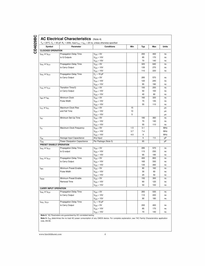
www.fairchildsemi.com 4
CD
402
9B
CAC Electrical Characteristics (Note 4)
TA = 25°C, CL = 50 pF, RL = 200k, Input trCL = tfCL = 20 ns, unless otherwise specified
Note 4: *AC Parameters are guaranteed by DC correlated testing.
Note 5: CPD determines the no load AC power consumption of any CMOS device. For complete explanation, see 74C Family Characteristics application
note, AN-90.
Symbol Parameter Conditions Min Typ Max Units
CLOCKED OPERATION
tPHL or tPLH Propagation Delay Time VDD = 5V 200 400 ns
to Q Outputs VDD = 10V 85 170 ns
VDD = 15V 70 140 ns
tPHL or tPLH Propagation Delay Time VDD = 5V 320 640 ns
to Carry Output VDD = 10V 135 270 ns
VDD = 15V 110 220 ns
tPHL or tPLH Propagation Delay Time CL = 15 pF
to Carry Output VDD = 5V 285 570 ns
VDD = 10V 120 240 ns
VDD = 15V 95 190 ns
tTHL or tTLH Transition Time/Q VDD = 5V 100 200 ns
or Carry Output VDD = 10V 50 100 ns
VDD = 15V 40 80 ns
tWH or tWL Minimum Clock VDD = 5V 160 320 ns
Pulse Width VDD = 10V 70 135 ns
VDD = 15V 55 110 ns
trCL or tfCL Maximum Clock Rise VDD = 5V 15 µs
and Fall Time VDD = 10V 10 µs
VDD = 15V 5 µs
tSU Minimum Set-Up Time VDD = 5V 180 360 ns
VDD = 10V 70 140 ns
VDD = 15V 55 110 ns
fCL Maximum Clock Frequency VDD = 5V 1.5 3.1 MHz
VDD = 10V 3.7 7.4 MHz
VDD = 15V 4.5 9 MHz
CIN Average Input Capacitance Any Input 5 7.5 pF
CPD Power Dissipation Capacitance Per Package (Note 5) 65 pF
PRESET ENABLE OPERATION
tPHL or tPLH Propagation Delay Time VDD = 5V 285 570 ns
to Q output VDD = 10V 115 230 ns
VDD = 15V 95 195 ns
tPHL or tPLH Propagation Delay Time VDD = 5V 400 800 ns
to Carry Output VDD = 10V 165 330 ns
VDD = 15V 135 260 ns
tWH Minimum Preset Enable VDD = 5V 80 160 ns
Pulse Width VDD = 10V 30 60 ns
VDD = 15V 25 50 ns
tREM Minimum Preset Enable VDD = 5V 150 300 ns
Removal Time VDD = 10V 60 120 ns
VDD = 15V 50 100 ns
CARRY INPUT OPERATION
tPHL or tPLH Propagation Delay Time VDD = 5V 265 530 ns
to Carry Output VDD = 10V 110 220 ns
VDD = 15V 90 180 ns
tPHL, tPLH Propagation Delay Time CL = 15 pF
to Carry Output VDD = 5V 200 400 ns
VDD = 10V 85 170 ns
VDD = 15V 70 140 ns
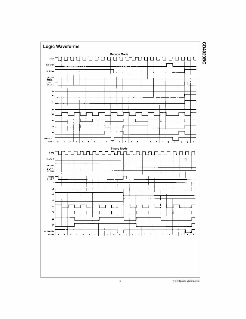
5 www.fairchildsemi.com
CD
40
29
BC
Logic Waveforms
Decade Mode
Binary Mode
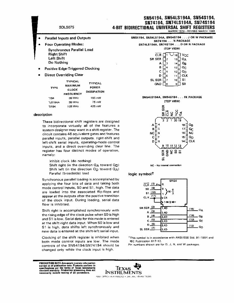
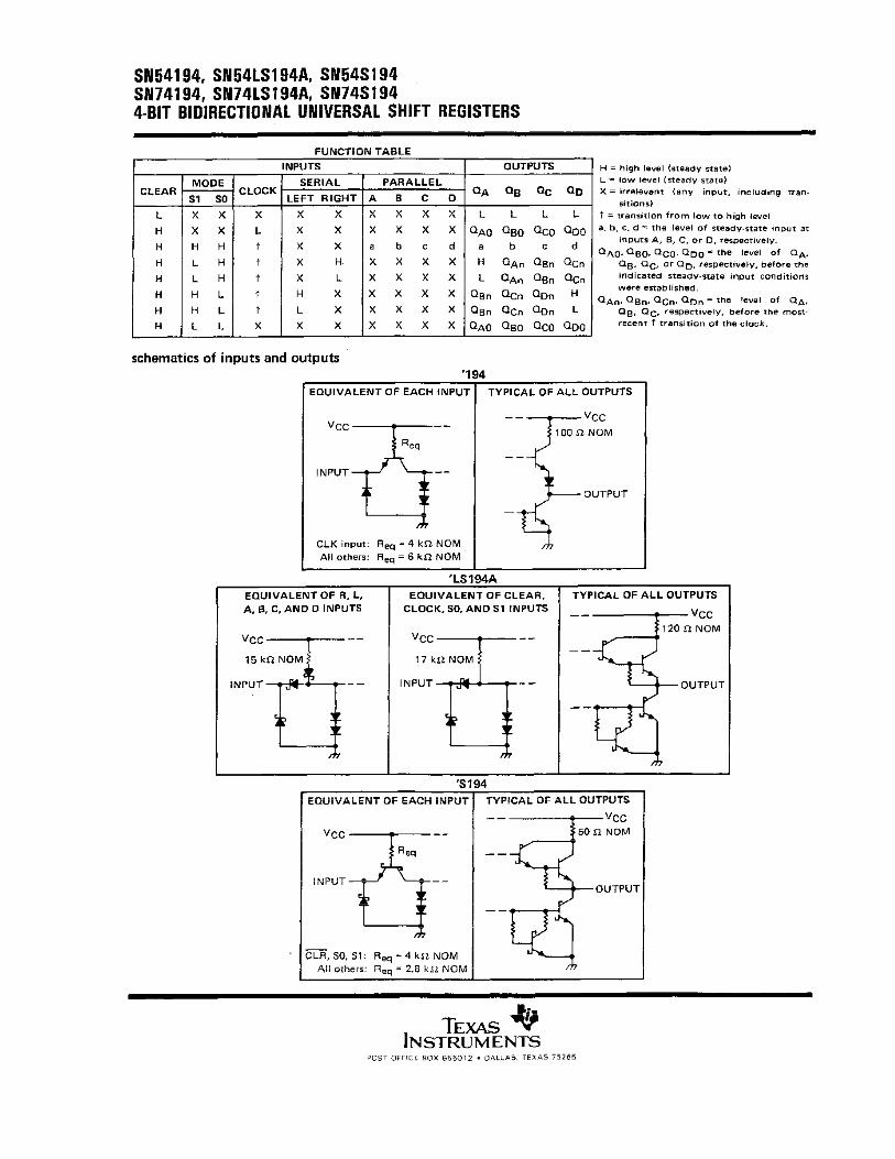

Prof. Dr. F. Dildey Dipl.-Ing. J.-C. Böhmke Fakultät Life Sciences
Praktikum Elektronik 2 Versuch 4
AD / DA - Wandlung
- 1 - Version 1.7
Stand WS 2012 / 2013
1 Lernziel Die Funktion und die Grenzen eines AD-Wandlers sowie eines DA-Wandlers sollen verstanden werden. Ferner sollen die grundlegenden Begriffe der AD-Wandlung verdeutlicht werden. Hierzu gehören u.a.
- die Umsetzung von positiven und negativen Spannungen, - die Auflösung - Fehler bei der AD-Wandlung
Bei der DA-Wandlung sollen zusätzlich die Begriffe Settling Time und Slew Rate erarbeitet werden. Das Lesen von Bauteilspezifikationen in den Datenblättern soll geübt werden.
2 Allgemeines Sehen Sie in die Datenblätter! Der Versuch 4 besteht aus drei Teilen:
• Teil A: Arbeiten mit dem Analog-Digitalwandler AD670 • Teil B: Arbeiten mit dem Digital-Analogwandler MAX 506C • Teil C: Kombination von AD-Wandler und DA-Wandler, Erfassung von Wandlungsartefakten
2.1 Teil A: Arbeiten mit dem Analog-Digitalwandler AD670
Eingesetzt wird ein 8-Bit-AD-Wandler vom Typ AD 670 der Firma Analog Devices. Der Taktgenerator und die Referenzspannungsquelle (2,56 V) sind auf dem Chip integriert. Der Hersteller gibt eine maximale Wandelzeit von 10μs an. Um die Wandlung zu starten, muss am Pin 13 (s. Datenblatt) ein Low-Impuls von mindestens 300 ns anliegen. Dieses Signal wird von einem Oszillator (Baustein NE 555) zyklisch erzeugt und kann an der Buchse „Int. Takt“ abgegriffen werden. Die Wiederholfrequenz kann über den Schalter S1 mit 20 kHz bzw. 40 kHz gewählt werden. Über den Schalter S2 (in Stellung Start) wird das Signal an den ADC gelegt. Wenn das Wandlerergebnis gelesen werden soll, muss das Signal am R/W-Eingang auf High gelegt werden. Hierzu muss der Schalter S2 in die Position 'STOP' gestellt werden. Die acht Leuchtdioden, die über ein Treiber-IC (74LS541) an den Ausgängen des ADC angeschlossen sind, zeigen das Ergebnis der Wandlung an. Zusätzlich zeigt der ADC am Pin 9 bei jeder Wandlung seinen Zustand an. Der Pin 9 ist mit der Buchse „Status“ verbunden. Dabei bedeuten: High > Wandlung läuft und Low > Wandlung beendet. Der AD 670 verfügt über folgende Betriebsarten: unipolar, bipolar, 2s complement, straight binary. Diese Betriebsarten lassen sich über Jumper auf der Platine umstecken. Die analogen Eingangsspannungen können aus dem Netzgerät entnommen werden.
2.2 Teil B: Arbeiten mit dem Digital-Analogwandler MAX 506C
Der Digital-Analog-Converter besteht aus einem Chip vom Typ MAX 506. Er wird in der hier vorgestellten Schaltung unipolar betrieben. Der MAX 506 ist ein 8 bit Wandler mit 4 Ausgängen. Die Bezeichnung "rail-to-rail" bedeutet, dass die Ausgangsspannung den Wert von +Ub und GND oder ±Ub bei symmetrischer Speisung annehmen kann. Über die Jumper S1 und S2 kann das Dateneingangslatch des jeweiligen Ausgangs adressiert werden. Stellen Sie die Jumper so ein, dass das zum Ausgang 1 gehörige Latch adressiert wird. Mit Hilfe des Jumpers S3 können Sie festlegen, ob Sie die Steuerleitung WR über den Taster „Man. Takt“ oder von einer externen Quelle ansteuern möchten.
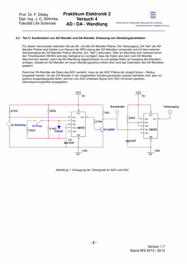
Prof. Dr. F. Dildey Dipl.-Ing. J.-C. Böhmke Fakultät Life Sciences
Praktikum Elektronik 2 Versuch 4
AD / DA - Wandlung
- 2 - Version 1.7
Stand WS 2012 / 2013
2.3 Teil C: Kombination von AD-Wandler und DA-Wandler, Erfassung von Wandlungsartefakten
Für diesen Versuchsteil verbinden Sie die AD- und die DA-Wandler-Platine. Der Taktausgang „DA-Takt“ der AD-Wandler-Platine wird hierbei zum Steuern der WR-Leitung des DA-Wandlers verwendet und mit dem externen Steuereingang der DA-Wandler-Platine (Buchse „Ext. Takt“) verbunden. Über ein Monoflop (hier realisiert durch den Timerbaustein NE555) wird das Taktsignal so verzögert, dass die Daten erst dann vom DA-Wandler übernommen werden, wenn die AD-Wandlung abgeschlossen ist und gültige Daten am Ausgang des Wandlers anliegen. Sobald am AD-Wandler ein neuer Wandlungszyklus initiiert wird, wird das Datenlatch des DA-Wandlers gesperrt. Damit der DA-Wandler die Daten des ADC versteht, muss an der ADC-Platine der straight binary – Modus eingestellt werden. Da der DA-Wandler in der vorgestellten Schaltungsvariante unipolar betrieben wird, also nur positive Ausgangssignale liefert, wird ein vom ADC erfasstes Signal vom DAC mit einem positiven Gleichspannungsoffset ausgegeben.
Abbildung 1: Erzeugung der Taktsignale für ADC und DAC

Prof. Dr. F. Dildey Dipl.-Ing. J.-C. Böhmke Fakultät Life Sciences
Praktikum Elektronik 2 Versuch 4
AD / DA - Wandlung
- 3 - Version 1.7
Stand WS 2012 / 2013
3 Aufgaben zur Vorbereitung des Praktikums Zur Vorbereitung dieses Versuchs müssen Sie sich über folgende Begriffe in Kenntnis setzen:
• AD-Wandlung (ADC) / DA-Wandlung (DAC) • Auflösung • Bitfehler • Abtastrate • speziell zum ADC:
• Wandlertypen (Zähl-, Wiege- und Parallelverfahren) • Umsetzzeit (Wandelzeit, conversion time) • bipolar- Modus • 2s Komplement ( Zweier - Komplement) (bipolar)
• speziell zum DAC:
• Output Settling Time • Slew Rate (siehe Datenblatt MAX 506C)
Schaltungsentwürfe und Rechenergebnisse zu Punkt 3 sind bei Praktikumsbeginn vorzulegen. Benutzen Sie hierfür die Lösungsbögen 1 und 2, Praktikumsvorbereitung.
3.1 Zum AD-Converter
3.1.1 Nach welchem Verfahren arbeitet der AD-Wandler vom Typ AD 670?
3.1.2 Als Eingang für das Analogsignal werden die Pins 16 und 18 verwendet. Wie groß ist bei dieser Konfiguration der Bereich für die Eingangsspannung im unipolaren und im bipolaren Modus? (Für die Antwort benötigen Sie das Datenblatt!)
3.1.3 Geben Sie an, wie und wo Sie die tatsächliche Wandelzeit messen wollen. Warum kann das Status-Signal nicht zum Takten des DA-Wandlers verwendet werden?
3.1.4 Berechnen sie aus den angegebenen Spannungswerten (s. Lösungsblatt 1) das entsprechende Bitmuster.
3.1.5 Was ist hinsichtlich des Verhältnisses von Abtastfrequenz und der höchsten im abzutastenden Signal enthaltenen Frequenz zu beachten?
3.2 Zum DA-Converter
3.2.1 Wie groß ist die Auflösung beim DAC MAX 506C bei einer einfachen Spannungsversorgung von +5V
und Vref = 5V?
3.2.2 Berechnen sie aus den angegebenen Bitmustern (s. Lösungsblatt 2) die entsprechenden Spannungswerte.
3.2.3 Was verstehen Sie unter Output Settling Time beim DAC MAX 506C?
3.2.4 Wie groß ist die Output Settling Time beim MAX 506C lt. Datenblatt?
3.2.5 Wie groß ist die Slew Rate beim DAC MAX 506C lt. Datenblatt?
3.2.6 Entwerfen Sie einen Versuchsaufbau, mit dem Sie die Output Settling Time und die Slew Rate des DAC MAX 506C messen können. Dabei soll, wie im Datenblatt vorgegeben, der Eingangswert von 0000 0000 auf 1111 1111 ständig hin- und herschalten. Zur Verfügung stehen Ihnen
- ein Funktionsgenerator,
- ein Oszilloskop,
- ein Netzteil,
- und der DAC MAX 506C.
3.3 Zusatzaufgabe
3.3.1 Eine Audio-CD wird mit 44,1 kHz abgetastet. Die Auflösung liegt bei 16 Bit. Berechnen Sie den Speicherplatz in kByte, der notwendig ist, um ein Stereo-Signal für eine Minute zu speichern.

Prof. Dr. F. Dildey Dipl.-Ing. J.-C. Böhmke Fakultät Life Sciences
Praktikum Elektronik 2 Versuch 4
AD / DA - Wandlung
- 4 - Version 1.7
Stand WS 2012 / 2013
4 Messaufgaben
4.1 Teil A: Arbeiten mit dem Analog-Digitalwandler AD670
4.1.1 Schließen sie die Platine mit dem AD-Wandler an die Festspannung von +5 V an. Schalten Sie den AD-Wandler in den unipolaren Modus. Als Ausgabeformat wählen Sie straight binary. Messen Sie die Steuersignale R/W und STATUS mit dem Oszilloskop in ihren Zeitverläufen möglichst genau aus. Dokumentieren Sie Ihre Ergebnisse mit der Oszilloskop-Software „Open Choice“.
4.1.2 Bestimmen Sie die Umsetzzeit.
4.1.3 Legen Sie Gleichspannungssignale von 0.005V, 0.01V, 1.0V, 2.0V, 2.55V und 2.6V nacheinander an den Eingang des ADC und nehmen Sie die dazugehörigen Bitmuster auf.
Um die sehr kleinen Gleichspannungssignale möglichst einfach einstellen zu können, schalten Sie den Spannungsteiler zwischen Netzteil und ADC-Eingang. Zur Messung der Gleichspannungssignale verwenden Sie bitte das Hameg Tischmultimeter. Vergleichen Sie die gemessenen Bitmuster mit Ihren theoretischen Ergebnissen aus 3.1.4.
Achten Sie darauf, dass die maximal zulässige Eingangsspannung nicht überschritten wird.
4.1.4 Wo liegen die Grenzen in der Auflösung? Können Sie bis auf 1 Bit genau wandeln?
4.1.5 Wie groß ist der Eingangsspannungsbereich?
4.2 Teil B: Arbeiten mit dem Digital-Analogwandler MAX 506C
Der analoge Ausgang des DAC ist VOUT A. 4.2.1 Legen Sie nacheinander Bitmuster von 0000 0000 bis 0000 1010 in 1-Bit-Schritten, 1000 0000 und
1111 1111 an den DA-Wandler, und messen Sie die dazugehörigen Ausgangsspannungen mit dem Multimeter. Vergleichen Sie sie mit Ihren theoretischen Ergebnissen aus 3.2.2.
4.2.2 Vergleichen sie die Schrittweite mit der errechneten Auflösung (siehe 3.2.1)
4.2.3 Ermitteln Sie nach Ihrem Messaufbau aus 3.2.5. die Output Settling Time und die Voltage-Output Slew Rate des DACs. Dokumentieren Sie Ihre Ergebnisse mit der Oszilloskop-Software „Open Choice“.
4.3 Kombination von AD-Wandler und DA-Wandler, Erfassung von Wandlungsartefakten
Schließen Sie die Ausgänge des AD-Wandlers in der richtigen Reihenfolge an die Dateneingänge des DA-Wandlers und verbinden Sie den Taktausgang der AD-Wandler-Platine mit dem externen Takteingang der DA-Wandler-Platine.
Konfigurieren Sie den AD-Wandler für den bipolaren Betrieb, Datenformat straight binary.
Wählen Sie zunächst mit dem Schalter S1 einen Arbeitstakt von 40 kHz. Lassen Sie den Wandler kontinuierlich wandeln (Schalter S2 in Stellung Wandlung).
An der DA-Wandler-Platine wählen Sie mit dem Jumper J3 die Ansteuerung über das externe Taktsignal aus (Buchse „Ext. Takt“).
4.3.1 Legen Sie ein sinusförmiges Wechselspannungssignal mit 2 VSS und einer Frequenz von 5 kHz an den Eingang des AD-Wandlers. Vergleichen Sie das Eingangssignal des AD-Wandlers und das Ausgangssignal des DA-Wandlers auf dem Oszilloskop. Reduzieren Sie nun die Taktfrequenz des Wandlungssystems auf 20 kHz, indem Sie an der AD-Wandler-Platine den Schalter S1 umschalten. Führen Sie den Ablauf nochmals für ein sinusförmiges Wechselspannungssignal mit 2 VSS und einer Frequenz von 200 Hz durch. Dokumentieren Sie Ihre Beobachtungen mit der Oszilloskop-Software „Open Choice“.
4.3.2 Wählen Sie mit Hilfe des Schalters S1 wieder einen Arbeitstakt von 40 kHz. Legen Sie ein sinusförmiges Wechselspannungssignal mit 2 VSS und einer Frequenz von 200 Hz bzw. 5 kHz an den Eingang des AD-Wandlers. Verringern Sie die Auflösung des DA-Wandlers, indem Sie niederwertige Biteingänge des DA-Wandlers vom AD-Wandler trennen und die Eingänge stattdessen an Masse legen. Dokumentieren Sie Ihre Beobachtungen erneut mit der Oszilloskop-Software „Open Choice“.
Prof. Dr. F. Dildey Dipl.-Ing. J.-C. Böhmke Fakultät Life Sciences
Praktikum Elektronik 2 Versuch 4
AD / DA - Wandlung
- 5 - Version 1.7
Stand WS 2012 / 2013
5 Anhang
5.1 Geräteliste
1x Platine ADC mit AD 670 1x Platine DAC mit MAX 506C 1x Oszilloskop Tektronix Typ TDS 2002C 1x Dreifachnetzgerät HAMEG Typ HM 7042-5 1x Funktionsgenerator HAMEG Typ HM 8030-6 1x Einbaumultimeter HAMEG Typ HM 8012 2x Handmultimeter Fluke 83 oder 83V
5.2 Literaturhinweise
Formelsammlung zur Vorlesung Elektronik von Prof. Dr. Dildey Halbleiter-Schaltungstechnik Tietze/Schenk Springer Verlag ISBN 3-540-56184-6 FB-Bibliothek Ele D3-25 Elektronik für Ingenieure E. Hering K. Bressler J. Gutekunst VDI Verlag ISBN 3-18-400909-2 FB-Bibliothek Ele A98 Datenblätter (siehe Anhang oder www.alldatasheet.com)) AD-Wandler AD670 DA-Wandler MAX506
5.3 Lösungsbögen und Datenblätter
Lösungsbögen und Datenblätter folgen auf den nächsten Seiten…

Prof. Dr. F. Dildey Dipl.-Ing. J.-C. Böhmke Fakultät Life Sciences
Praktikum Elektronik 2 Lösungsbögen zu
Versuch 4
- 1 - Version 1.7
Stand SS 2012
1. Vorbereitung
zu 3.1.1. Wandlungsverfahren:
zu 3.1.2. Eingangsspannungsbereich:
zu 3.1.3. Messung der Wandlungszeit:
zu 3.1.4. Wandlungsergebnisse:
Eingang Ausgang Bitmuster theoretisch
Spannung in Volt D7 D6 D5 D4 D3 D2 D1 D0 0,005 0,010 1,000 2,000 2,550 2,600
zu 3.1.5. Abtastfrequenz ↔ Signalfrequenz:
zu 3.2.1. Auflösung des DAC:
Prof. Dr. F. Dildey Dipl.-Ing. J.-C. Böhmke Fakultät Life Sciences
Praktikum Elektronik 2 Lösungsbögen zu
Versuch 4
- 2 - Version 1.7
Stand SS 2012
zu 3.2.2. Ausgangsspannungen:
Eingang Ausgang
D7 D6 D5 D4 D3 D2 D1 D0 Spannung in Volt 0 0 0 0 0 0 0 0 0 0 0 0 0 0 0 1 0 0 0 0 0 0 1 0 0 0 0 0 0 0 1 1 0 0 0 0 0 1 0 0 0 0 0 0 0 1 0 1
zu 3.2.3. Begriffsdefinition Output Settling Time:
zu 3.2.4. Output Settling Time:
zu 3.2.5. Slew Rate:
Prof. Dr. F. Dildey Dipl.-Ing. J.-C. Böhmke Fakultät Life Sciences
Praktikum Elektronik 2 Lösungsbögen zu
Versuch 4
- 3 - Version 1.7
Stand SS 2012
zu 3.2.6. Messaufbau:
zu 3.3.1. Speicherplatzbedarf:
Prof. Dr. F. Dildey Dipl.-Ing. J.-C. Böhmke Fakultät Life Sciences
Praktikum Elektronik 2 Lösungsbögen zu
Versuch 4
- 4 - Version 1.7
Stand SS 2012
2. Versuchsdurchführung
zu 4.1.1. Steuersignale:
siehe Ausdruck Nr. Kommentar
zu 4.1.2. Umsetzzeit:
zu 4.1.3. AD-Wandlung:
Eingang Ausgang Ausgang Bitmuster theoretisch Bitmuster gemessen
Spannung in Volt D7 D6 D5 D4 D3 D2 D1 D0 D7 D6 D5 D4 D3 D2 D1 D0 0,005 0,010 1,000 2,000 2,550 2,600
Kommentar:
zu 4.1.4. Auflösungsgrenzen:
zu 4.1.2. Eingangsspannungsbereich:
Prof. Dr. F. Dildey Dipl.-Ing. J.-C. Böhmke Fakultät Life Sciences
Praktikum Elektronik 2 Lösungsbögen zu
Versuch 4
- 5 - Version 1.7
Stand SS 2012
zu 4.2.1. DA-Wandlung:
Eingang Ausgang Ausgang theoretisch gemessen
D7 D6 D5 D4 D3 D2 D1 D0 Spannung in Volt Spannung in Volt 0 0 0 0 0 0 0 0 0 0 0 0 0 0 0 1 0 0 0 0 0 0 1 0 0 0 0 0 0 0 1 1 0 0 0 0 0 1 0 0 0 0 0 0 0 1 0 1 0 0 0 0 0 1 1 0 0 0 0 0 0 1 1 1 0 0 0 0 1 0 0 0 0 0 0 0 1 0 0 1 0 0 0 0 1 0 1 0 1 0 0 0 0 0 0 0 1 1 1 1 1 1 1 1
zu 4.2.2. Schrittweite ↔ Auflösung:
zu 4.2.3. Slew Rate und Output Settling Time:
siehe Ausdruck Nr. Kommentar
zu 4.3.1. Einfluss der Abtastfrequenz:
siehe Ausdruck Nr. Kommentar
zu 4.3.2. Einfluss der Auflösung:
siehe Ausdruck Nr. Kommentar

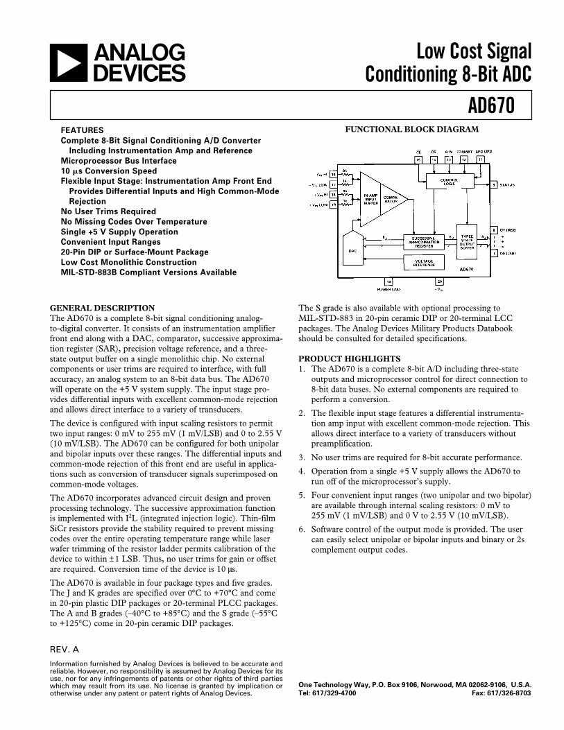
FUNCTIONAL BLOCK DIAGRAM
REV. A
Information furnished by Analog Devices is believed to be accurate andreliable. However, no responsibility is assumed by Analog Devices for itsuse, nor for any infringements of patents or other rights of third partieswhich may result from its use. No license is granted by implication orotherwise under any patent or patent rights of Analog Devices.
a Low Cost SignalConditioning 8-Bit ADC
AD670FEATURES
Complete 8-Bit Signal Conditioning A/D Converter
Including Instrumentation Amp and Reference
Microprocessor Bus Interface
10 ms Conversion Speed
Flexible Input Stage: Instrumentation Amp Front End
Provides Differential Inputs and High Common-Mode
Rejection
No User Trims Required
No Missing Codes Over Temperature
Single +5 V Supply Operation
Convenient Input Ranges
20-Pin DIP or Surface-Mount Package
Low Cost Monolithic Construction
MIL-STD-883B Compliant Versions Available
GENERAL DESCRIPTION
The AD670 is a complete 8-bit signal conditioning analog-to-digital converter. It consists of an instrumentation amplifierfront end along with a DAC, comparator, successive approxima-tion register (SAR), precision voltage reference, and a three-state output buffer on a single monolithic chip. No externalcomponents or user trims are required to interface, with fullaccuracy, an analog system to an 8-bit data bus. The AD670will operate on the +5 V system supply. The input stage pro-vides differential inputs with excellent common-mode rejectionand allows direct interface to a variety of transducers.
The device is configured with input scaling resistors to permittwo input ranges: 0 mV to 255 mV (1 mV/LSB) and 0 to 2.55 V(10 mV/LSB). The AD670 can be configured for both unipolarand bipolar inputs over these ranges. The differential inputs andcommon-mode rejection of this front end are useful in applica-tions such as conversion of transducer signals superimposed oncommon-mode voltages.
The AD670 incorporates advanced circuit design and provenprocessing technology. The successive approximation functionis implemented with I2L (integrated injection logic). Thin-filmSiCr resistors provide the stability required to prevent missingcodes over the entire operating temperature range while laserwafer trimming of the resistor ladder permits calibration of thedevice to within ±1 LSB. Thus, no user trims for gain or offsetare required. Conversion time of the device is 10 µs.
The AD670 is available in four package types and five grades.The J and K grades are specified over 0°C to +70°C and comein 20-pin plastic DIP packages or 20-terminal PLCC packages.The A and B grades (–40°C to +85°C) and the S grade (–55°Cto +125°C) come in 20-pin ceramic DIP packages.
One Technology Way, P.O. Box 9106, Norwood, MA 02062-9106, U.S.A.
Tel: 617/329-4700 Fax: 617/326-8703
The S grade is also available with optional processing toMIL-STD-883 in 20-pin ceramic DIP or 20-terminal LCCpackages. The Analog Devices Military Products Databookshould be consulted for detailed specifications.
PRODUCT HIGHLIGHTS
1. The AD670 is a complete 8-bit A/D including three-stateoutputs and microprocessor control for direct connection to8-bit data buses. No external components are required toperform a conversion.
2. The flexible input stage features a differential instrumenta-tion amp input with excellent common-mode rejection. Thisallows direct interface to a variety of transducers withoutpreamplification.
3. No user trims are required for 8-bit accurate performance.
4. Operation from a single +5 V supply allows the AD670 torun off of the microprocessor’s supply.
5. Four convenient input ranges (two unipolar and two bipolar)are available through internal scaling resistors: 0 mV to255 mV (1 mV/LSB) and 0 V to 2.55 V (10 mV/LSB).
6. Software control of the output mode is provided. The usercan easily select unipolar or bipolar inputs and binary or 2scomplement output codes.
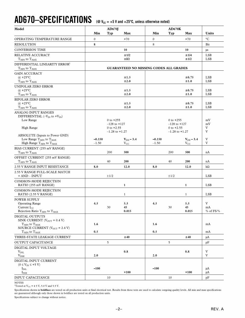
Model AD670J AD670K
Min Typ Max Min Typ Max Units
OPERATING TEMPERATURE RANGE 0 +70 0 +70 °C
RESOLUTION 8 8 Bit
CONVERSION TIME 10 10 µs
RELATIVE ACCURACY 61/2 61/4 LSB
TMIN to TMAX 6l/2 61/2 LSB
DIFFERENTIAL LINEARITY ERROR1
TMIN to TMAX GUARANTEED NO MISSING CODES ALL GRADES
GAIN ACCURACY
@ +25°C 61.5 60.75 LSB
TMIN to TMAX 62.0 61.0 LSB
UNIPOLAR ZERO ERROR
@ +25°C 61.5 60.75 LSB
TMIN to TMAX 62.0 61.0 LSB
BIPOLAR ZERO ERROR
@ +25°C 61.5 60.75 LSB
TMIN to TMAX 62.0 61.0 LSB
ANALOG INPUT RANGES
DIFFERENTIAL (–VIN to +VIN)
Low Range 0 to +255 0 to +255 mV
–128 to +127 –128 to +127 mV
High Range 0 to +2.55 0 to +2.55 V
–1.28 to +1.27 –1.28 to +1.27 V
ABSOLUTE (Inputs to Power GND)
Low Range TMIN to TMAX –0.150 VCC – 3.4 –0.150 VCC – 3.4 V
High Range TMIN to TMAX –1.50 VCC –1.50 VCC V
BIAS CURRENT (255 mV RANGE)
TMIN to TMAX 200 500 200 500 nA
OFFSET CURRENT (255 mV RANGE)
TMIN to TMAX 40 200 40 200 nA
2.55 V RANGE INPUT RESISTANCE 8.0 12.0 8.0 12.0 kΩ
2.55 V RANGE FULL-SCALE MATCH
+ AND – INPUT ±1/2 ±1/2 LSB
COMMON-MODE REJECTION
RATIO (255 mV RANGE) 1 1 LSB
COMMON-MODE REJECTION
RATIO (2.55 V RANGE) 1 1 LSB
POWER SUPPLY
Operating Range 4.5 5.5 4.5 5.5 V
Current ICC 30 45 30 45 mA
Rejection Ratio TMIN to TMAX 0.015 0.015 % of FS/%
DIGITAL OUTPUTS
SINK CURRENT (VOUT = 0.4 V)
TMIN to TMAX 1.6 1.6 mA
SOURCE CURRENT (VOUT = 2.4 V)
TMIN to TMAX 0.5 0.5 mA
THREE-STATE LEAKAGE CURRENT 640 640 µA
OUTPUT CAPACITANCE 5 5 pF
DIGITAL INPUT VOLTAGE
VINL 0.8 0.8 V
VINH 2.0 2.0 V
DIGITAL INPUT CURRENT
(0 ≤ VIN ≤ +5 V)
IINL –100 –100 µA
IINH +100 +100 µA
INPUT CAPACITANCE 10 10 pF
NOTES1Tested at VCC = 4 5 V, 5.0 V and 5.5 V.
Specifications shown in boldface are tested on all production units at final electrical test. Results from those tests are used to calculate outgoing quality levels. All min and max specifications
are guaranteed although only those shown in boldface are tested on all production units.
Specifications subject to change without notice.
AD670–SPECIFICATIONS (@ VCC = +5 V and +258C, unless otherwise noted)
REV. A–2–
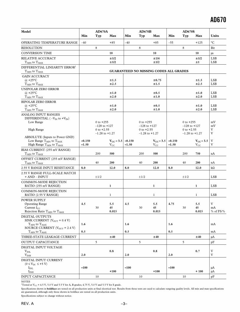
Model AD670A AD670B AD670S
Min Typ Max Min Typ Max Min Typ Max Units
OPERATING TEMPERATURE RANGE –40 +85 –40 +85 –55 +125 °C
RESOLUTION 8 8 8 Bit
CONVERSION TIME 10 10 10 µs
RELATIVE ACCURACY 61/2 61/4 61/2 LSB
TMIN to TMAX 61/2 61/2 61 LSB
DIFFERENTIAL LINEARITY ERROR1
TMIN to TMAX GUARANTEED NO MISSING CODES ALL GRADES
GAIN ACCURACY
@ +25°C 61.5 60.75 61.5 LSB
TMIN to TMAX 62.5 61.5 62.5 LSB
UNIPOLAR ZERO ERROR
@ +25°C 61.0 60.5 61.0 LSB
TMIN to TMAX 62.0 61.0 62.0 LSB
BIPOLAR ZERO ERROR
@ +25°C 61.0 60.5 61.0 LSB
TMIN to TMAX 62.0 61.0 62.0 LSB
ANALOG INPUT RANGES
DIFFERENTIAL ( –VIN to +VIN)
Low Range 0 to +255 0 to +255 0 to +255 mV
–128 to +127 –128 to +127 –128 to +127 mV
High Range 0 to +2.55 0 to +2.55 0 to +2.55 V
–1.28 to +1.27 –1.28 to +1.27 –1.28 to +1.27 V
ABSOLUTE (Inputs to Power GND)
Low Range TMIN to TMAX –0.150 VCC – 3.5 –0.150 VCC – 3.5 –0.150 VCC – 3.5 V
High Range TMIN to TMAX –1.50 VCC –1.50 VCC –1.50 VCC V
BIAS CURRENT (255 mV RANGE)
TMIN to TMAX 200 500 200 500 200 750 nA
OFFSET CURRENT (255 mV RANGE)
TMIN to TMAX 40 200 40 200 40 200 nA
2.55 V RANGE INPUT RESISTANCE 8.0 12.0 8.0 12.0 8.0 12.0 kΩ
2.55 V RANGE FULL-SCALE MATCH
+ AND – INPUT ±1/2 ±1/2 ±1/2 LSB
COMMON-MODE REJECTION
RATIO (255 mV RANGE) 1 1 1 LSB
COMMON-MODE REJECTION
RATIO (2.55 V RANGE) 1 1 1 LSB
POWER SUPPLY
Operating Range 4.5 5.5 4.5 5.5 4.75 5.5 V
Current ICC 30 45 30 45 30 45 mA
Rejection Ratio TMIN to TMAX 0.015 0.015 0.015 % of FS/%
DIGITAL OUTPUTS
SINK CURRENT (VOUT = 0.4 V)
TMIN to TMAX 1.6 1.6 1.6 mA
SOURCE CURRENT (VOUT = 2.4 V)
TMIN to TMAX 0.5 0.5 0.5 mA
THREE-STATE LEAKAGE CURRENT 640 640 640 µA
OUTPUT CAPACITANCE 5 5 5 pF
DIGITAL INPUT VOLTAGE
VINL 0.8 0.8 0.7 V
VINH 2.0 2.0 2.0 V
DIGITAL INPUT CURRENT
(0 ≤ VIN ≤ +5 V)
IINL –100 –100 –100 µA
IINH +100 +100 + 100 µA
INPUT CAPACITANCE 10 10 10 pF
NOTES1Tested at VCC = 4.5 V, 5.0 V and 5.5 V for A, B grades; 4.75 V, 5.0 V and 5.5 V for S grade.
Specifications shown in boldface are tested on all production units at final electrical test. Results from those tests are used to calculate outgoing quality levels. All min and max specifications
are guaranteed, although only those shown in boldface are tested on all production units.
Specifications subject to change without notice.
AD670
REV. A –3–
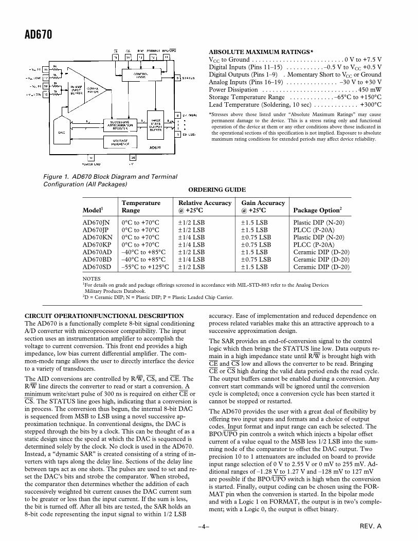
AD670
REV. A–4–
ORDERING GUIDE
Temperature Relative Accuracy Gain AccuracyModel1 Range @ +258C @ +258C Package Option2
AD670JN 0°C to +70°C ±1/2 LSB ±1.5 LSB Plastic DIP (N-20)AD670JP 0°C to +70°C ±1/2 LSB ±1.5 LSB PLCC (P-20A)AD670KN 0°C to +70°C ±1/4 LSB ±0.75 LSB Plastic DIP (N-20)AD670KP 0°C to +70°C ±1/4 LSB ±0.75 LSB PLCC (P-20A)AD670AD –40°C to +85°C ±1/2 LSB ±1.5 LSB Ceramic DIP (D-20)AD670BD –40°C to +85°C ±1/4 LSB ±0.75 LSB Ceramic DIP (D-20)AD670SD –55°C to +125°C ±1/2 LSB ±1.5 LSB Ceramic DIP (D-20)
NOTES1For details on grade and package offerings screened in accordance with MIL-STD-883 refer to the Analog Devices
Military Products Databook.2D = Ceramic DIP; N = Plastic DIP; P = Plastic Leaded Chip Carrier.
Figure 1. AD670 Block Diagram and Terminal
Configuration (AII Packages)
ABSOLUTE MAXIMUM RATINGS*
VCC to Ground . . . . . . . . . . . . . . . . . . . . . . . . . . . 0 V to +7.5 VDigital Inputs (Pins 11–15) . . . . . . . . . . . –0.5 V to VCC +0.5 VDigital Outputs (Pins 1–9) . Momentary Short to VCC or GroundAnalog Inputs (Pins 16–19) . . . . . . . . . . . . . . . –30 V to +30 VPower Dissipation . . . . . . . . . . . . . . . . . . . . . . . . . . . . 450 mWStorage Temperature Range . . . . . . . . . . . . . –65°C to +150°CLead Temperature (Soldering, 10 sec) . . . . . . . . . . . . . +300°C
*Stresses above those listed under “Absolute Maximum Ratings” may cause
permanent damage to the device. This is a stress rating only and functional
operation of the device at them or any other conditions above those indicated in
the operational sections of this specification is not implied. Exposure to absolute
maximum rating conditions for extended periods may affect device reliability.
CIRCUIT OPERATION/FUNCTIONAL DESCRIPTION
The AD670 is a functionally complete 8-bit signal conditioningA/D converter with microprocessor compatibility. The inputsection uses an instrumentation amplifier to accomplish thevoltage to current conversion. This front end provides a highimpedance, low bias current differential amplifier. The com-mon-mode range allows the user to directly interface the deviceto a variety of transducers.
The AID conversions are controlled by R/W, CS, and CE. TheR/W line directs the converter to read or start a conversion. Aminimum write/start pulse of 300 ns is required on either CE orCS. The STATUS line goes high, indicating that a conversion isin process. The conversion thus begun, the internal 8-bit DACis sequenced from MSB to LSB using a novel successive ap-proximation technique. In conventional designs, the DAC isstepped through the bits by a clock. This can be thought of as astatic design since the speed at which the DAC is sequenced isdetermined solely by the clock. No clock is used in the AD670.Instead, a “dynamic SAR” is created consisting of a string of in-verters with taps along the delay line. Sections of the delay linebetween taps act as one shots. The pulses are used to set and re-set the DAC’s bits and strobe the comparator. When strobed,the comparator then determines whether the addition of eachsuccessively weighted bit current causes the DAC current sumto be greater or less than the input current. If the sum is less,the bit is turned off. After all bits are tested, the SAR holds an8-bit code representing the input signal to within 1/2 LSB
accuracy. Ease of implementation and reduced dependence onprocess related variables make this an attractive approach to asuccessive approximation design.
The SAR provides an end-of-conversion signal to the controllogic which then brings the STATUS line low. Data outputs re-main in a high impedance state until R/W is brought high withCE and CS low and allows the converter to be read. BringingCE or CS high during the valid data period ends the read cycle.The output buffers cannot be enabled during a conversion. Anyconvert start commands will be ignored until the conversioncycle is completed; once a conversion cycle has been started itcannot be stopped or restarted.
The AD670 provides the user with a great deal of flexibility byoffering two input spans and formats and a choice of outputcodes. Input format and input range can each be selected. TheBPO/UPO pin controls a switch which injects a bipolar offsetcurrent of a value equal to the MSB less 1/2 LSB into the sum-ming node of the comparator to offset the DAC output. Twoprecision 10 to 1 attenuators are included on board to provideinput range selection of 0 V to 2.55 V or 0 mV to 255 mV. Ad-ditional ranges of –1.28 V to 1.27 V and –128 mV to 127 mVare possible if the BPO/UPO switch is high when the conversionis started. Finally, output coding can be chosen using the FOR-MAT pin when the conversion is started. In the bipolar modeand with a Logic 1 on FORMAT, the output is in two’s comple-ment; with a Logic 0, the output is offset binary.
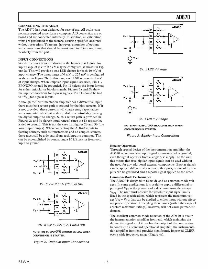
AD670
REV. A –5–
CONNECTING THE AD670
The AD670 has been designed for ease of use. All active com-ponents required to perform a complete A/D conversion are onboard and are connected internally. In addition, all calibrationtrims are performed at the factory, assuring specified accuracywithout user trims. There are, however, a number of optionsand connections that should be considered to obtain maximumflexibility from the part.
INPUT CONNECTIONS
Standard connections are shown in the figures that follow. Aninput range of 0 V to 2.55 V may be configured as shown in Fig-ure 2a. This will provide a one LSB change for each 10 mV ofinput change. The input range of 0 mV to 255 mV is configuredas shown in Figure 2b. In this case, each LSB represents 1 mVof input change. When unipolar input signals are used, Pin 11,BPO/UPO, should be grounded. Pin 11 selects the input formatfor either unipolar or bipolar signals. Figures 3a and 3b showthe input connections for bipolar signals. Pin 11 should be tiedto +VCC for bipolar inputs.
Although the instrumentation amplifier has a differential input,there must be a return path to ground for the bias currents. If itis not provided, these currents will charge stray capacitancesand cause internal circuit nodes to drift uncontrollably causingthe digital output to change. Such a return path is provided inFigures 2a and 3a (larger input ranges) since the 1k resistor legis tied to ground. This is not the case for Figures 2b and 3b (thelower input ranges). When connecting the AD670 inputs tofloating sources, such as transformers and ac-coupled sources,there must still be a dc path from each input to common. Thiscan be accomplished by connecting a 10 kΩ resistor from eachinput to ground.
2a. 0 V to 2.55 V (10 mV/LSB)
2b. 0 mV to 255 mV (1 mV/LSB)
NOTE: PIN 11, BPO/UPO SHOULD BE LOW WHEN
CONVERSION IS STARTED.
Figure 2. Unipolar Input Connections
3a. ±1.28 V Range
3b. ±128 mV Range
NOTE: PIN 11, BPO/UPO SHOULD BE HIGH WHEN
CONVERSION IS STARTED.
Figure 3. Bipolar Input Connections
Bipolar Operation
Through special design of the instrumentation amplifier, theAD670 accommodates input signal excursions below ground,even though it operates from a single 5 V supply. To the user,this means that true bipolar input signals can be used withoutthe need for any additional external components. Bipolar signalscan be applied differentially across both inputs, or one of the in-puts can be grounded and a bipolar signal applied to the other.
Common-Mode Performance
The AD670 is designed to reject dc and ac common-mode volt-ages. In some applications it is useful to apply a differential in-put signal VIN in the presence of a dc common-mode voltageVCM. The user must observe the absolute input signal limitslisted in the specifications, which represent the maximum volt-age VIN + VCM that can be applied to either input without affect-ing proper operation. Exceeding these limits (within the range ofabsolute maximum ratings), however, will not cause permanentdamage.
The excellent common-mode rejection of the AD670 is due tothe instrumentation amplifier front end, which maintains thedifferential signal until it reaches the output of the comparator.In contrast to a standard operational amplifier, the instrumenta-tion amplifier front end provides significantly improved CMRRover a wide frequency range (Figure 4a).
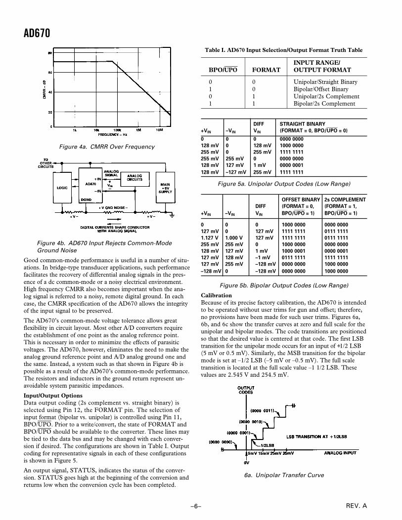
AD670
REV. A–6–
Table I. AD670 Input Selection/Output Format Truth Table
INPUT RANGE/
BPO/UPO FORMAT OUTPUT FORMAT
0 0 Unipolar/Straight Binary1 0 Bipolar/Offset Binary0 1 Unipolar/2s Complement1 1 Bipolar/2s Complement
DIFF STRAIGHT BINARY
+VIN –VIN VIN (FORMAT = 0, BPO/UPO = 0)
0 0 0 0000 0000
128 mV 0 128 mV 1000 0000
255 mV 0 255 mV 1111 1111
255 mV 255 mV 0 0000 0000
128 mV 127 mV 1 mV 0000 0001
128 mV –127 mV 255 mV 1111 1111
Figure 5a. Unipolar Output Codes (Low Range)
OFFSET BINARY 2s COMPLEMENT
DIFF (FORMAT = 0, (FORMAT = 1,
+VIN –VIN VIN BPO/UPO = 1) BPO/UPO = 1)
0 0 0 1000 0000 0000 0000
127 mV 0 127 mV 1111 1111 0111 1111
1.127 V 1.000 V 127 mV 1111 1111 0111 1111
255 mV 255 mV 0 1000 0000 0000 0000
128 mV 127 mV 1 mV 1000 0001 0000 0001
127 mV 128 mV –1 mV 0111 1111 1111 1111
127 mV 255 mV –128 mV 0000 0000 1000 0000
–128 mV 0 –128 mV 0000 0000 1000 0000
Figure 5b. Bipolar Output Codes (Low Range)
Calibration
Because of its precise factory calibration, the AD670 is intendedto be operated without user trims for gun and offset; therefore,no provisions have been made for such user trims. Figures 6a,6b, and 6c show the transfer curves at zero and full scale for theunipolar and bipolar modes. The code transitions are positionedso that the desired value is centered at that code. The first LSBtransition for the unipolar mode occurs for an input of +1/2 LSB(5 mV or 0.5 mV). Similarly, the MSB transition for the bipolarmode is set at –1/2 LSB (–5 mV or –0.5 mV). The full scaletransition is located at the full scale value –1 1/2 LSB. Thesevalues are 2.545 V and 254.5 mV.
6a. Unipolar Transfer Curve
Figure 4a. CMRR Over Frequency
Figure 4b. AD670 Input Rejects Common-Mode
Ground Noise
Good common-mode performance is useful in a number of situ-ations. In bridge-type transducer applications, such performancefacilitates the recovery of differential analog signals in the pres-ence of a dc common-mode or a noisy electrical environment.High frequency CMRR also becomes important when the ana-log signal is referred to a noisy, remote digital ground. In eachcase, the CMRR specification of the AD670 allows the integrityof the input signal to be preserved.
The AD670’s common-mode voltage tolerance allows greatflexibility in circuit layout. Most other A/D converters requirethe establishment of one point as the analog reference point.This is necessary in order to minimize the effects of parasiticvoltages. The AD670, however, eliminates the need to make theanalog ground reference point and A/D analog ground one andthe same. Instead, a system such as that shown in Figure 4b ispossible as a result of the AD670’s common-mode performance.The resistors and inductors in the ground return represent un-avoidable system parasitic impedances.
Input/Output Options
Data output coding (2s complement vs. straight binary) isselected using Pin 12, the FORMAT pin. The selection ofinput format (bipolar vs. unipolar) is controlled using Pin 11,BPO/UPO. Prior to a write/convert, the state of FORMAT andBPO/UPO should be available to the converter. These lines maybe tied to the data bus and may be changed with each conver-sion if desired. The configurations are shown in Table I. Outputcoding for representative signals in each of these configurationsis shown in Figure 5.
An output signal, STATUS, indicates the status of the conver-sion. STATUS goes high at the beginning of the conversion andreturns low when the conversion cycle has been completed.
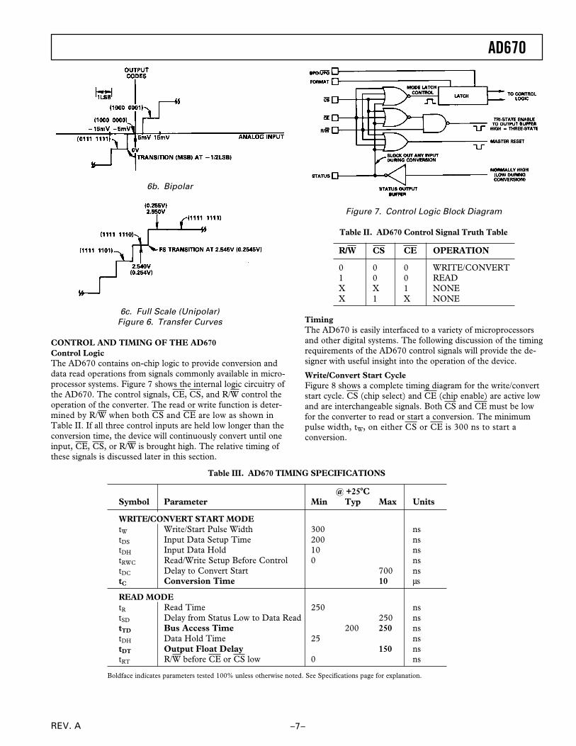
AD670
REV. A –7–
Table III. AD670 TIMING SPECIFICATIONS
@ +258CSymbol Parameter Min Typ Max Units
WRITE/CONVERT START MODE
tW Write/Start Pulse Width 300 nstDS Input Data Setup Time 200 nstDH Input Data Hold 10 nstRWC Read/Write Setup Before Control 0 nstDC Delay to Convert Start 700 nstC Conversion Time 10 µs
READ MODE
tR Read Time 250 nstSD Delay from Status Low to Data Read 250 nstTD Bus Access Time 200 250 nstDH Data Hold Time 25 nstDT Output Float Delay 150 nstRT R/W before CE or CS low 0 ns
Boldface indicates parameters tested 100% unless otherwise noted. See Specifications page for explanation.
6b. Bipolar
6c. Full Scale (Unipolar)
Figure 6. Transfer Curves
CONTROL AND TIMING OF THE AD670
Control Logic
The AD670 contains on-chip logic to provide conversion anddata read operations from signals commonly available in micro-processor systems. Figure 7 shows the internal logic circuitry ofthe AD670. The control signals, CE, CS, and R/W control theoperation of the converter. The read or write function is deter-mined by R/W when both CS and CE are low as shown inTable II. If all three control inputs are held low longer than theconversion time, the device will continuously convert until oneinput, CE, CS, or R/W is brought high. The relative timing ofthese signals is discussed later in this section.
Figure 7. Control Logic Block Diagram
Table II. AD670 Control Signal Truth Table
R/W CS CE OPERATION
0 0 0 WRITE/CONVERT1 0 0 READX X 1 NONEX 1 X NONE
Timing
The AD670 is easily interfaced to a variety of microprocessorsand other digital systems. The following discussion of the timingrequirements of the AD670 control signals will provide the de-signer with useful insight into the operation of the device.
Write/Convert Start Cycle
Figure 8 shows a complete timing diagram for the write/convertstart cycle. CS (chip select) and CE (chip enable) are active lowand are interchangeable signals. Both CS and CE must be lowfor the converter to read or start a conversion. The minimumpulse width, tW, on either CS or CE is 300 ns to start aconversion.
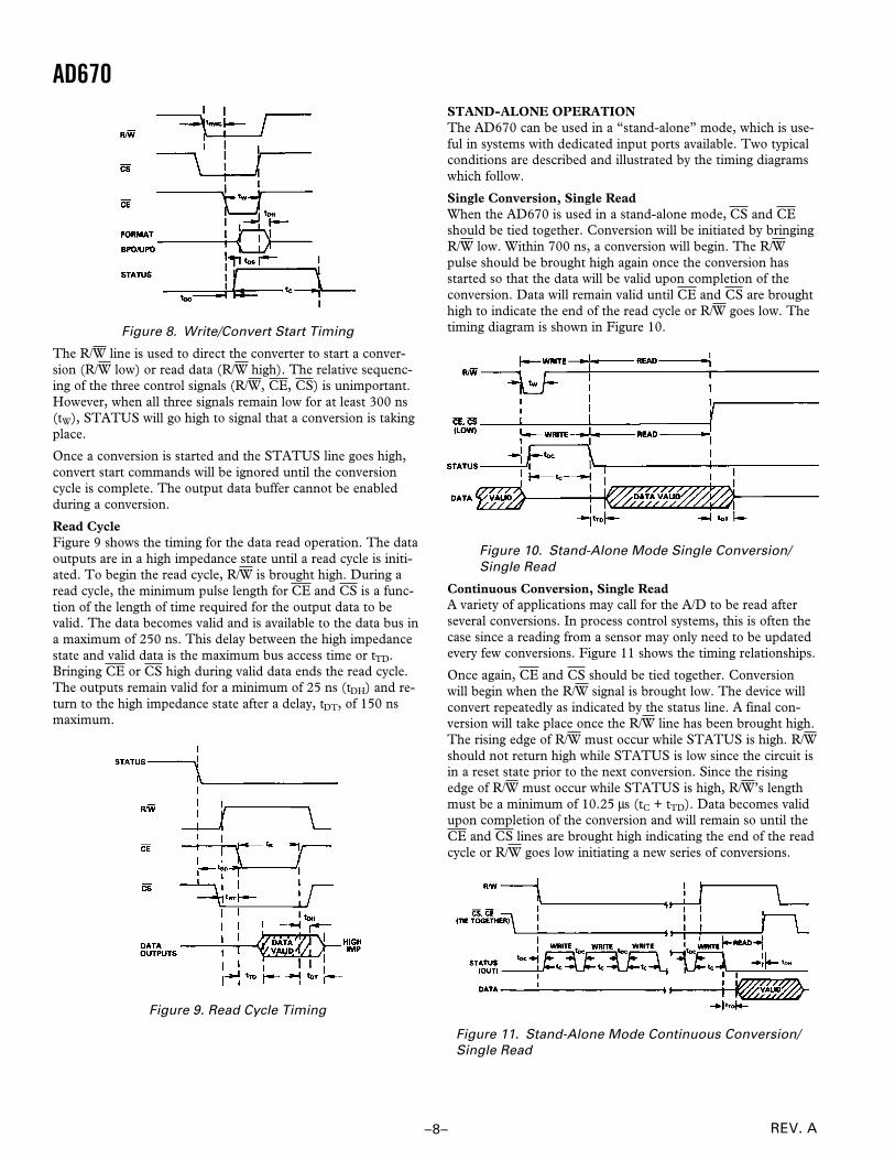
AD670
REV. A–8–
Figure 8. Write/Convert Start Timing
The R/W line is used to direct the converter to start a conver-sion (R/W low) or read data (R/W high). The relative sequenc-ing of the three control signals (R/W, CE, CS) is unimportant.However, when all three signals remain low for at least 300 ns(tW), STATUS will go high to signal that a conversion is takingplace.
Once a conversion is started and the STATUS line goes high,convert start commands will be ignored until the conversioncycle is complete. The output data buffer cannot be enabledduring a conversion.
Read Cycle
Figure 9 shows the timing for the data read operation. The dataoutputs are in a high impedance state until a read cycle is initi-ated. To begin the read cycle, R/W is brought high. During aread cycle, the minimum pulse length for CE and CS is a func-tion of the length of time required for the output data to bevalid. The data becomes valid and is available to the data bus ina maximum of 250 ns. This delay between the high impedancestate and valid data is the maximum bus access time or tTD.Bringing CE or CS high during valid data ends the read cycle.The outputs remain valid for a minimum of 25 ns (tDH) and re-turn to the high impedance state after a delay, tDT, of 150 nsmaximum.
Figure 9. Read Cycle Timing
STAND-ALONE OPERATION
The AD670 can be used in a “stand-alone” mode, which is use-ful in systems with dedicated input ports available. Two typicalconditions are described and illustrated by the timing diagramswhich follow.
Single Conversion, Single Read
When the AD670 is used in a stand-alone mode, CS and CE
should be tied together. Conversion will be initiated by bringingR/W low. Within 700 ns, a conversion will begin. The R/Wpulse should be brought high again once the conversion hasstarted so that the data will be valid upon completion of theconversion. Data will remain valid until CE and CS are broughthigh to indicate the end of the read cycle or R/W goes low. Thetiming diagram is shown in Figure 10.
Figure 10. Stand-Alone Mode Single Conversion/
Single Read
Continuous Conversion, Single Read
A variety of applications may call for the A/D to be read afterseveral conversions. In process control systems, this is often thecase since a reading from a sensor may only need to be updatedevery few conversions. Figure 11 shows the timing relationships.
Once again, CE and CS should be tied together. Conversionwill begin when the R/W signal is brought low. The device willconvert repeatedly as indicated by the status line. A final con-version will take place once the R/W line has been brought high.The rising edge of R/W must occur while STATUS is high. R/Wshould not return high while STATUS is low since the circuit isin a reset state prior to the next conversion. Since the risingedge of R/W must occur while STATUS is high, R/W’s lengthmust be a minimum of 10.25 µs (tC + tTD). Data becomes validupon completion of the conversion and will remain so until theCE and CS lines are brought high indicating the end of the readcycle or R/W goes low initiating a new series of conversions.
Figure 11. Stand-Alone Mode Continuous Conversion/
Single Read
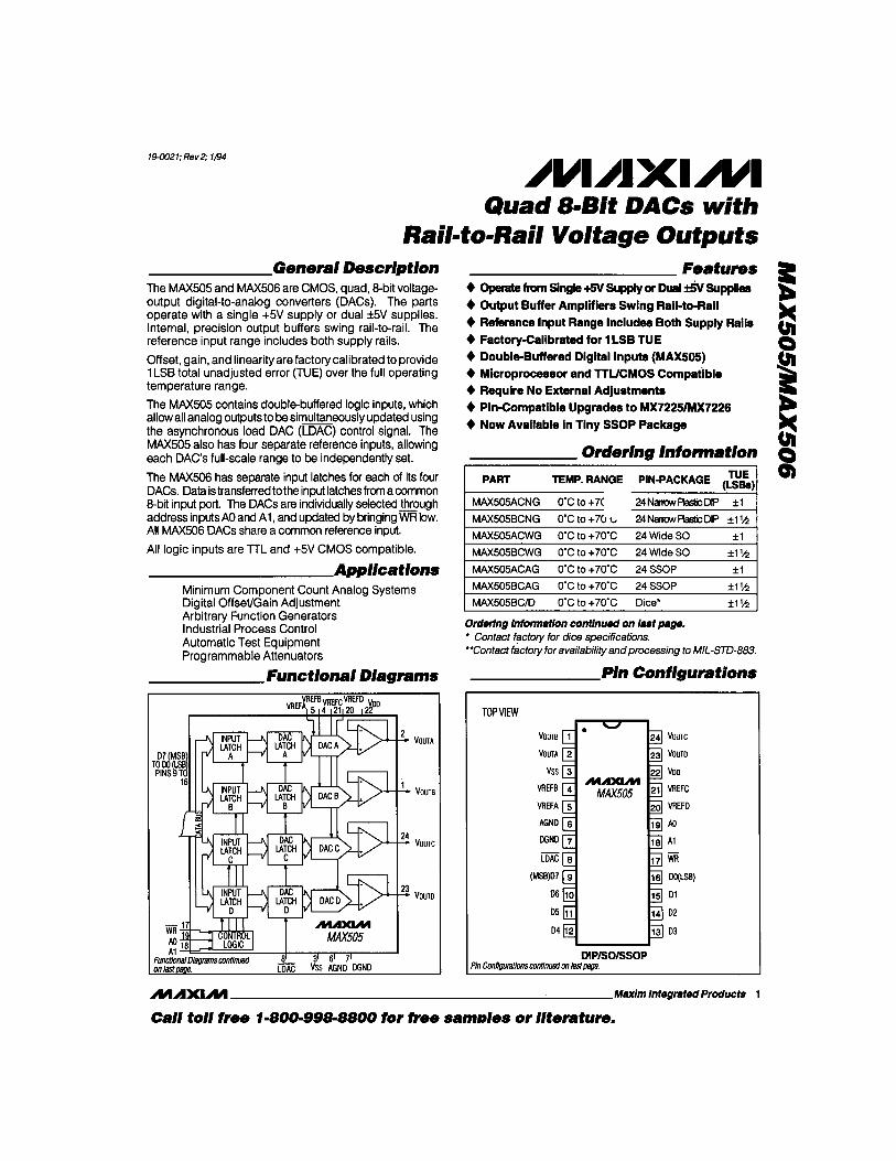
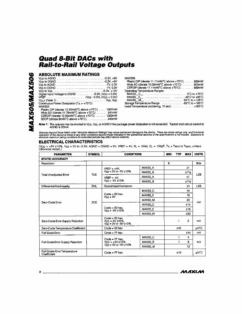
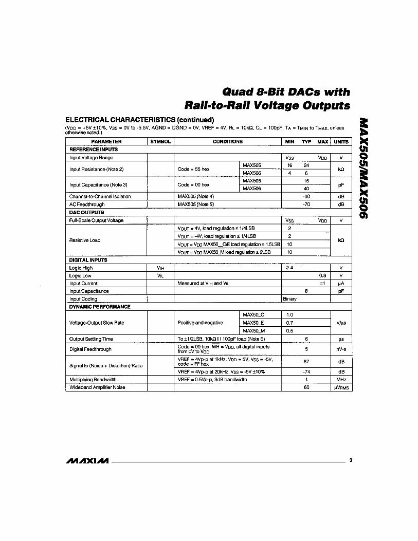
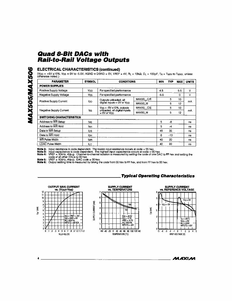
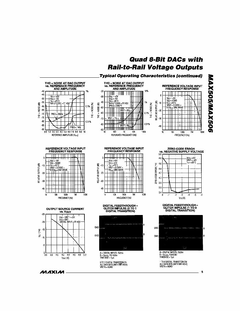
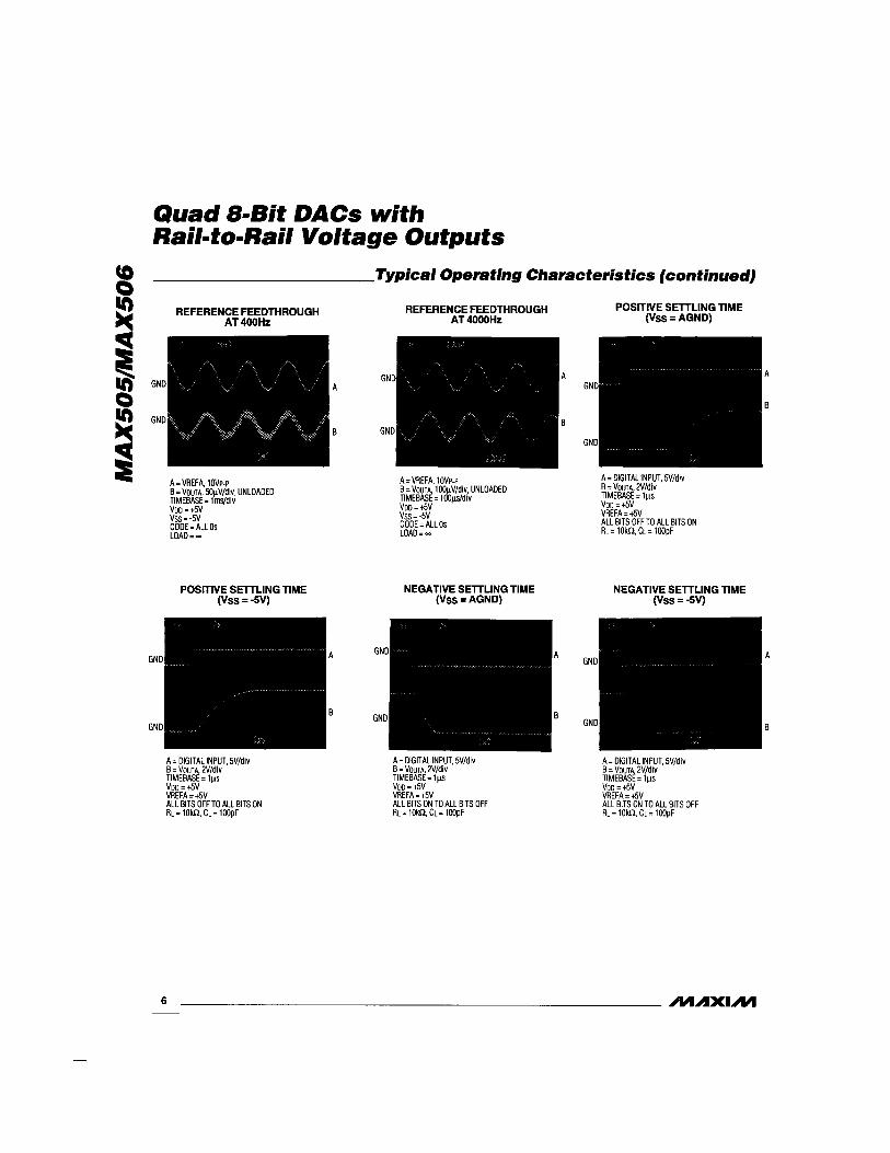
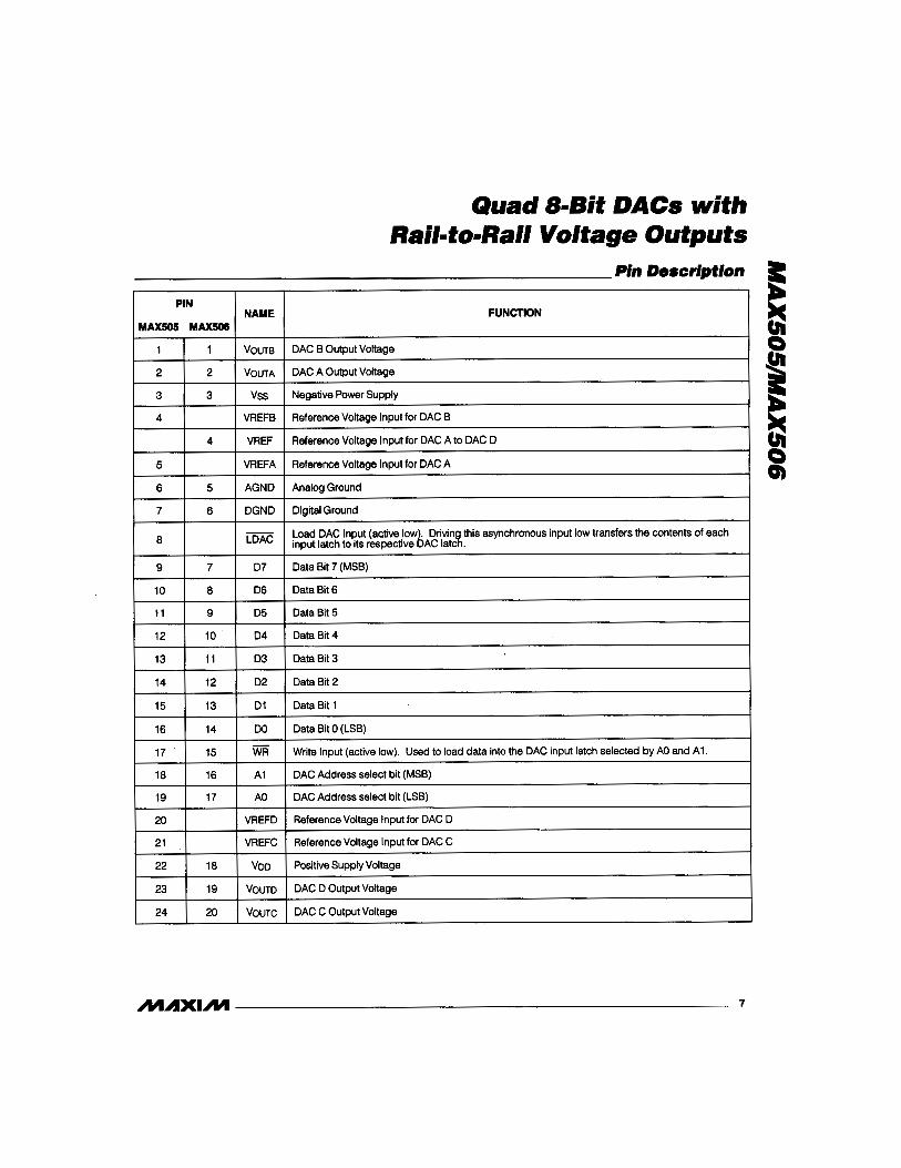
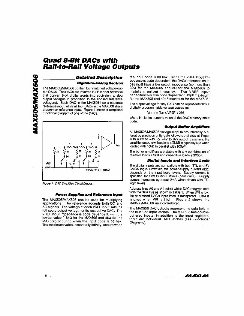
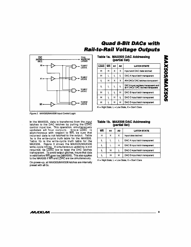

Prof. Dr. F. Dildey Dipl.-Ing. J.-C. Böhmke Fakultät Life Sciences
Praktikum Elektronik 2 Versuch 5
Simulation digitaler Schaltkreise
- 1 von 5 - Version 1.3 Stand WS 2012 / 2013
1. Lernziel Dieser Versuch soll mit der Technik und den Möglichkeiten der rechnergestützten Simulation digitaler Schaltungen vertraut machen. Die Schaltungen werden mit einem Grafik-Editor eingegeben und unter verschiedenen Aspekten analysiert. Durch Variation einzelner Parameter wird ihr Einfluss auf die Eigenschaften der Schaltung analysiert. Ferner soll das Arbeiten mit Wortgenerator und Logikanalysator geübt werden.
2. Allgemeines Zur Vorbereitung dieses Versuchsteils müssen Sie sich über folgende Begriffe in Kenntnis setzen: • Wahrheitstabelle • boolsche Gleichungen • logische Grundschaltkreise AND, OR, NAND, NOR • D-, RS-, JK-FLIP-FLOP • asynchrone Binärzähler • Schieberegister • Dekoder • Multiplexer Eine kurze Einführung in die Bedienung des Simulationsprogramms MULTISIM 10 finden Sie im Kapitel 5. Der Hersteller National Instruments stellt auf der Website www.ni.com eine Demoversion des Programms zur Verfügung. Hierzu ist eine kostenfreie Registrierung erforderlich.
3. Vorbereitung Diesen Versuch sollen Sie selbst gestalten. Deshalb wird in der Praktikumsvorbereitung von Ihnen eine eigene Versuchsbeschreibung gefordert. Es sollten mindestens folgende Themen von Ihnen bearbeitet werden: 1. Zusammenschaltung von einfachen logischen Bauteilen. 2. D-Flip-Flop 3. Aufbau eines asynchronen Zählers 4. Aufbau eines Schieberegisters oder Dekoders oder Multiplexer oder anderer ähnlich komplexer
Schaltungen 5. eine beliebige Wahrheitstabelle, die schaltungstechnisch realisiert werden soll und für sie überschaubar
ist 6. eine beliebige boolsche Gleichung, die schaltungstechnisch realisiert werden soll und für Sie
überschaubar ist Sie können jedoch auch hierzu entsprechende Alternativen erarbeiten. Entwerfen Sie Schaltungen zu den genannten Themen und überlegen Sie sich, wie Sie die Funktion der Schaltungen überprüfen wollen. Sehen Sie als Signalquelle und Messgerät Wortgenerator und Logikanalysator vor. Ihre Schaltungsentwürfe und Ihre gewählten Messaufgaben sind bei Praktikumsbeginn vorzulegen.
4. Messaufgaben Hier müssen Ihre selbst gewählten Messaufgaben in Abhängigkeit Ihrer Schaltungen folgen. Dokumentieren Sie Ihre Versuche, indem Sie die Schaltbilder und die Messergebnisse des Logikanalysators ausdrucken. Hierbei macht es Sinn, auch die Eingangssignale Ihrer Schaltungen mit Hilfe des Logikanalysators zu erfassen.
Prof. Dr. F. Dildey Dipl.-Ing. J.-C. Böhmke Fakultät Life Sciences
Praktikum Elektronik 2 Versuch 5
Simulation digitaler Schaltkreise
- 2 von 5 - Version 1.3 Stand WS 2012 / 2013
5. Hinweise zur Bedienung der Simulationssoftware Melden Sie sich als Benutzer Elektronik an. Es wird kein Passwort benötigt. Starten Sie das Simulationsprogramm Multisim.
Die wichtigsten Bauelemente finden Sie bereits in den Symbolleisten am oberen Rand des Arbeitsfeldes. Einzelne Gatter und Flip-Flops finden Sie unter „Sonstige Digitaldaten platzieren“ rechts neben den CMOS- und TTL-Bauelementen.
Einige nützliche Tastenkürzel sind: Hilfe...................................... F1 Ausschneiden....................... Strg + X Kopieren............................... Strg + C Einfügen .............................. Strg + V Drehen................................. Strg + R Spiegeln Horizontal.............. Alt + X Spiegeln Vertikal.................. Alt + Y Bezeichnen.......................... Strg + B
Ziehen Sie die Bauteile aus der Bauteilübersicht auf Ihr Arbeitsfeld. Die Verbindungen „löten“ Sie, indem Sie die Endpunkte mit der linken Maustaste anklicken und den entstehenden Draht zum Endpunkt des nächsten Bauteils ziehen (siehe Abb.1).
Abbildung 1: Bedienoberfläche Multisim
Prof. Dr. F. Dildey Dipl.-Ing. J.-C. Böhmke Fakultät Life Sciences
Praktikum Elektronik 2 Versuch 5
Simulation digitaler Schaltkreise
- 3 von 5 - Version 1.3 Stand WS 2012 / 2013
Bevor Sie Ihre Schaltung aufbauen, sollten Sie zur Überprüfung Ihrer boolschen Gleichungen den Logikkonverter benutzen, den Sie in der Toolbox am rechten Bildschirmrand finden. Der Logikkonverter bietet die Möglichkeit, aus Wahrheitstabellen boolsche Gleichungen zu erstellen, umgekehrt zu Ihren Gleichungen Wahrheitstabellen zu erstellen sowie aus der Gleichung die Schaltung zu generieren.
Nach dem Aufbau Ihrer Schaltung können Sie zur Überprüfung der Funktion bei einfachen Verknüpfungen die Indikatorlämpchen verwenden, die Sie in der Toolbox mittig am oberen Bildschirmrand finden, und die Eingangssignale mit Hilfe von Schaltern vorgeben. Bei komplexeren Schaltungen empfiehlt sich die Verwendung von Wortgenerator und Logikanalysator. Mit Hilfe des Wortgenerators lassen sich verschiedene Bitmuster generieren, so dass alle benötigten Eingangszustände zyklisch abgerufen werden können. Mit Hilfe des Logikanalysators können – ähnlich wie bei einem Oszilloskop – an verschiedenen Stellen der Schaltung gleichzeitig die Signalpegel erfasst und zeitlich verfolgt werden. Im Gegensatz zum Oszilloskop verfügt der Logikanalysator über 32 Eingänge, allerdings unterscheidet er nur die Pegel High und Low. Die empfohlenen Einstellungen entnehmen Sie bitte den folgenden Abbildungen. Zunächst die Konfiguration des Wortgenerators:
Abbildung 3: Festlegung der Ausgabefrequenz und der Bitfolge des Wortgenerators
Abbildung 2: Optionen des Logikkonverters
Prof. Dr. F. Dildey Dipl.-Ing. J.-C. Böhmke Fakultät Life Sciences
Praktikum Elektronik 2 Versuch 5
Simulation digitaler Schaltkreise
- 4 von 5 - Version 1.3 Stand WS 2012 / 2013
Am rechten Rand von Abb. 3 ist das gewählte Bitmuster zu erkennen (die Darstellung ist hier hexadezimal – sie kann wahlweise auch binär eingestellt werden): Startpunkt ist bei hex 00, der Wortgenerator zählt hoch bis hex 03. Hier ist der Endpunkt gesetzt und der Wortgenerator springt zurück zum Startpunkt. In der erweiterten Konfiguration des Wortgenerators müssen noch die Zählrichtung und das Anfangsbitmuster eingestellt werden (siehe Abb. 4).
Bei der Konfiguration des Logikanalysators wählen Sie bitte 10 Taktsignale / Skalenteil und definieren Sie die Takteinstellungen gemäß Abb. 5. Bitte schalten Sie über den Button „Reverse“ bzw. „Invertieren“ die Hintergrundfarbe auf weiß um, um beim Ausdruck nicht unnötig viel schwarze Druckerfarbe zu verbrauchen.
Über den Button „Definieren“ bzw. „Set“ gelangen Sie in die erweiterte Taktkonfiguration – übernehmen Sie bitte die dargestellten Werte:
Abbildung 4: erweiterte Konfiguration des Bitmustergenerators
Abbildung 5: Logikanalysator
Prof. Dr. F. Dildey Dipl.-Ing. J.-C. Böhmke Fakultät Life Sciences
Praktikum Elektronik 2 Versuch 5
Simulation digitaler Schaltkreise
- 5 von 5 - Version 1.3 Stand WS 2012 / 2013
Nun sind die erforderlichen Parameter konfiguriert und Sie können mit Ihren Messungen beginnen.
6. Anhang
6.1 Geräteliste
1x PC mit Pentium i7 CPU 2,8GHz, 8GB RAM mit Windows 7 oder vergleichbar 1x Simulationssoftware Multisim
6.2 Literaturhinweise
Tietze/Schenk Halbleiterschaltungstechnik Springer Verlag ISBN 3-540-42849-6 L.Palotas Elektronik für Ingenieure: Analoge und digitale integrierte Schaltungen Vieweg Verlag ISBN 978-3528039158 Formelsammlung zur Vorlesung Elektronik von Prof. Dr. Dildey National Instruments (NI) Multisim 10 Getting Started.pdf (kann auch im Labor eingesehen werden)
E. Hering K. Bressle J. Gutekunst Elektronik für Ingenieure Springer Verlag ISBN 3-540-41738-9 H.Hinsch Elektronik-Ein Werkzeug für Naturwissenschaftler Springer Verlag ISBN 978-3540613602
Abbildung 6: Taktkonfiguration des Logikanalysators


Prof. Dr. F. Dildey Dipl.-Ing. J.-C. Böhmke Fakultät Life Sciences
Praktikum Elektronik 2 Versuch 6
FPGAs und ihre Anwendung
- 1 von 3 - Version 1.2 Stand WS 2012 / 2013
1. Lernziel Im Verlauf des Versuchs sollen Sie die Design-Möglichkeiten, die mit einem FPGA (Field Programmable Gate Array - "Vor Ort modifizierbarer Logikbaustein") möglich sind, kennen lernen.
2. Allgemeines
Ein FPGA ist ein programmierbarer Integrierter Schaltkreis (IC) der Digitaltechnik. In FPGAs können durch spezifische Konfiguration interner Strukturen die verschiedenartigsten kundenspezifischen Schaltungen gebildet werden. Dabei hat sich in den letzten Jahren der Anwendungsbereich von der klassischen "Glue-Logic", also der reinen Verbindungslogik zwischen verschiedenen digitalen Baugruppen, zunehmend erweitert. Heutzutage werden FPGAs auch bei mittleren Stückzahlen für die Realisierung komplexer digitaler Schaltungen bis hin zu kompletten digitalen Systemen eingesetzt.
Durch die Rekonfigurierbarkeit von FPGAs direkt im Gerät bei dem Endanwender besteht darüber hinaus der wesentliche Vorteil, auf aktuelle technische Entwicklungen reagieren zu können und die digitalen Schaltungen durch Updates anpassen zu können, ohne direkt die zugrunde liegende Hardware der FPGA-Chips verändern zu müssen. Ferner lässt sich der Platzbedarf einer Schaltung im Gegensatz zum herkömmlichen Aufbau aus diversen einzelnen ICs deutlich verringern. Da die Funktion des FPGAs ausschließlich durch die Konfiguration festgelegt wird, kann der gleiche Baustein für viele verschiedene Schaltungen und Anwendungen verwendet werden. Er kann deshalb in großen Stückzahlen produziert werden, was ihn bei Prototypen und Kleinserien sehr kostengünstig im Vergleich zu einer Anwendungsspezifischen Integrierten Schaltung (ASIC) macht.
Vor dem Zeitalter der FPGAs war die Anfertigung von Anwendungsspezifischen Integrierten Schaltungen (ASIC) nur durch die Halbleiterhersteller direkt möglich. Dieses Verfahren war daher nur bei sehr großen Stückzahlen kosteneffizient. Ferner waren diese Schaltungen nachträglich nicht mehr modifizierbar; ein kleiner Fehler bei der Schaltungsentwicklung machte die Schaltung unbrauchbar und führte somit zu hohen Folgekosten. Für Kleinserien blieb daher nur der Aufbau der Schaltungen aus einzelnen ICs - hierdurch stieg der Platzbedarf jedoch enorm an. Ferner war eine nachträgliche Schaltungsmodifikation ebenfalls nur sehr schwer und mit hohen Folgekosten realisierbar.
3. Schaltungsbeschreibung Der hier vorgestellte Baustein ispLSI1016E verfügt über 32 IO-Pins, die wahlweise als Eingangs-, Ausgangs- oder bidirektionaler Anschlusspin konfiguriert werden können. Auf der Versuchsplatine (siehe Abb.1 im Anhang) sind die Pins 3-10 als Eingänge vorgesehen. Sie können mittels der Schalter auf High- und Low-Pegel geschaltet werden; eine LED zeigt dabei den jeweiligen Zustand des Pegels an. Falls Sie eigene Schaltungen anschließen möchten, können Sie die Schalter von den Pins durch Ziehen der Jumper trennen; einem Anschluss individueller Schaltungen direkt über die gelben Eingangsbuchsen steht dann nichts im Wege. Für diverse Schaltwerke (z.B. Flip-Flops) benötigt der FPGA einen Takt zur Synchronisation – daher ist Pin 11 als globaler Takteingang vorbereitet. Die Pins 37-44 sind als Ausgänge vorbereitet. Die Ausgangssignale können über die grünen Buchsen abgegriffen werden. Zusätzlich ist ein Treiber-IC mit den Pins verbunden, über das der aktuell anliegende Pegel an den Pins auf den LEDs abgebildet wird. Die Pins 15-32 sind nicht weiter vorkonfiguriert und können von Ihnen sowohl als Ein- oder als Ausgang betrieben werden.

Prof. Dr. F. Dildey Dipl.-Ing. J.-C. Böhmke Fakultät Life Sciences
Praktikum Elektronik 2 Versuch 6
FPGAs und ihre Anwendung
- 2 von 3 - Version 1.2 Stand WS 2012 / 2013
4. Vorbereitung In Anlehnung an den Versuch "Schaltnetze" sollen Sie eine Alarmanlage entwerfen. 4.1 Grundschaltung
Ihre Alarmanlage soll 2 Türkontakte, 3 Fensterkontakte sowie einen Dämmerungssensor beinhalten. Die Tür- und Fensterkontakte sollen im geöffneten Zustand Low-Pegel haben, der Dämmerungsschalter habe bei Tag High-Pegel. Nur bei Dunkelheit soll beim Öffnen einer oder mehrerer Türen und / oder Fenster eine Sirene aktiviert werden.
4.2 Erweiterung der Anlage um einen Alarmspeicher
Erweitern Sie die Anlage um einen Alarmspeicher. Falls ein Alarm ausgelöst wurde, soll er gespeichert bleiben, bis über einen Schalter (High im gedrückten Zustand) der Alarm quittiert wird. Die Sirene soll weiterhin nur während des eigentlichen Alarmereignisses aktiv sein.
4.3 Austausch eines defekten Türkontakts
Einer der Türkontakte an Ihrer Anlage aus 4.2 geht kaputt; Sie bekommen leider nicht mehr den Originalkontakt. Der Ersatzkontakt habe im geöffneten Zustand High-Pegel. Passen Sie die Anlage an den neuen Türkontakt an.
4.4 Scharf-Schalten der Alarmanlage am Wochenende
Der Kunde möchte über einen Schalter die Anlage aus 4.3 am Wochenende auch tagsüber scharf schalten können.
Bitte entwerfen Sie Schaltbilder zu allen 4 Schaltungsvarianten, stellen Sie die boolschen Gleichungen für die Logikteile auf und erstellen Sie Funktionstabellen zu Ihren Schaltungen. Die Schaltungsentwürfe und Rechenergebnisse sind bei Praktikumsbeginn vorzulegen.
5. Messaufgaben Sie erhalten zu Beginn des Versuchs eine kurze Einweisung in das Programmiertool des FPGAs. Des Weiteren finden Sie an Ihrem Arbeitsplatz eine Kurzanleitung zur Bedienung des Programmiertools. Folgen Sie dieser Anleitung, um unnötige Fehler zu vermeiden. Übertragen Sie Ihre Schaltungsentwürfe mit Hilfe des Schaltplaneingabemoduls, welches Ihren Schaltplan in eine für den FPGA verständliche Programmiersprache übersetzt, in den FPGA. Dokumentieren Sie Ihre Schaltpläne sowie die Pinbelegung des FPGAs und überprüfen Sie die Funktion Ihrer Schaltung.
Prof. Dr. F. Dildey Dipl.-Ing. J.-C. Böhmke Fakultät Life Sciences
Praktikum Elektronik 2 Versuch 6
FPGAs und ihre Anwendung
- 3 von 3 - Version 1.2 Stand WS 2012 / 2013
6. Anhang
6.1 Geräteliste
1x PC mit Pentium i7 CPU 2,8GHz, 8GB RAM mit Windows 7 oder vergleichbar 1x Simulationssoftware Multisim
6.2 Literaturhinweise
Tietze/Schenk Halbleiterschaltungstechnik Springer Verlag ISBN 3-540-42849-6 L.Palotas Elektronik für Ingenieure: Analoge und digitale integrierte Schaltungen Vieweg Verlag ISBN 978-3528039158 Formelsammlung zur Vorlesung Elektronik von Prof. Dr. Dildey Kurzanleitung zur Programmierung der FPGAs (kann im Labor eingesehen werden)
E. Hering K. Bressle J. Gutekunst Elektronik für Ingenieure Springer Verlag ISBN 3-540-41738-9 H.Hinsch Elektronik-Ein Werkzeug für Naturwissenschaftler Springer Verlag ISBN 978-3540613602
6.3 Platinenansicht
Abbildung 1 - Frontansicht der Platine
6.4 Datenblätter
Datenblätter folgen auf den nächsten Seiten.

ispLSI®
1016EAIn-System Programmable High Density PLD
1016ea_02.1 1
USE is
pMACH 4
A5
FOR N
EW
5V D
ESIGNS
Features
• HIGH-DENSITY PROGRAMMABLE LOGIC
— 2000 PLD Gates— 32 I/O Pins, One Dedicated Input— 96 Registers
— High-Speed Global Interconnect— Wide Input Gating for Fast Counters, State
Machines, Address Decoders, etc.— Small Logic Block Size for Random Logic— Functionally Compatible with ispLSI 1016E
• NEW FEATURES
— 100% IEEE 1149.1 Boundary Scan Testable
— ispJTAG™ In-System Programmable via IEEE 1149.1
(JTAG) Test Access Port
— User-Selectable 3.3V or 5V I/O Supports Mixed-
Voltage Systems (VCCIO Pin)
— Open-Drain Output Option
• HIGH-PERFORMANCE E2CMOS® TECHNOLOGY
— fmax = 200 MHz Maximum Operating Frequency— tpd = 4.5 ns Propagation Delay— TTL Compatible Inputs and Outputs— Electrically Erasable and Reprogrammable— Non-Volatile— 100% Tested at Time of Manufacture— Unused Product Term Shutdown Saves Power
• IN-SYSTEM PROGRAMMABLE
— Increased Manufacturing Yields, Reduced Time-to-Market and Improved Product Quality
— Reprogram Soldered Device for Faster Prototyping
• OFFERS THE EASE OF USE AND FAST SYSTEMSPEED OF PLDs WITH THE DENSITY AND FLEXIBILITYOF FIELD PROGRAMMABLE GATE ARRAYS
— Complete Programmable Device Can Combine GlueLogic and Structured Designs
— Enhanced Pin Locking Capability— Three Dedicated Clock Input Pins— Synchronous and Asynchronous Clocks— Programmable Output Slew Rate Control to
Minimize Switching Noise— Flexible Pin Placement— Optimized Global Routing Pool Provides Global
Interconnectivity
Functional Block Diagram
CLK
A0
A1
A2
A3
A4
A5
A6
A7
B7
B6
B5
B4
B3
B2
B1
B0
Outp
ut R
outing P
ool
Outp
ut R
outing P
ool
Global Routing Pool (GRP)
Logic
Array
D Q
D Q
D Q
D Q
GLB
0139C/1016EA
Description
The ispLSI 1016EA is a High Density Programmable
Logic Device containing 96 Registers, 32 Universal I/O
pins, one Dedicated Input pin, two Dedicated Clock Input
pins, one Global OE input pin and a Global Routing Pool
(GRP). The GRP provides complete interconnectivity
between all of these elements. The ispLSI 1016EA fea-
tures 5V in-system programmability (ISP™) and in-system
diagnostic capabilities via an IEEE 1149.1 Test Access
Port. The ispLSI 1016EA offers non-volatile
reprogrammability of the logic, as well as the intercon-
nect to provide truly reconfigurable systems. A functional
superset of the ispLSI 1016 architecture, the ispLSI
1016EA device adds user-selectable 3.3V or 5V I/O and
open-drain output options.
The basic unit of logic on the ispLSI 1016EA device is the
Generic Logic Block (GLB). The GLBs are labeled A0,
A1...B7 (Figure 1). There are a total of 16 GLBs in the
ispLSI 1016EA device. Each GLB has 18 inputs, a
programmable AND/OR/Exclusive OR array, and four
outputs which can be configured to be either combinato-
rial or registered. Inputs to the GLB come from the GRP
and a dedicated input. All of the GLB outputs are brought
back into the GRP so that they can be connected to the
inputs of any other GLB on the device.
Copyright © 2007 Lattice Semiconductor Corp. All brand or product names are trademarks or registered trademarks of their respective holders. The specifications and information herein are subject
to change without notice.
LATTICE SEMICONDUCTOR CORP., 5555 Northeast Moore Ct., Hillsboro, Oregon 97124, U.S.A.
Tel. (503) 268-8000; 1-800-LATTICE; FAX (503) 268-8556; http://www.latticesemi.com
April 2007
2
Specifications ispLSI 1016EA
USE is
pMACH 4
A5
FOR N
EW
5V D
ESIGNS
Functional Block Diagram
Figure 1. ispLSI 1016EA Functional Block Diagram
The device also has 32 I/O cells, each of which is directly
connected to an I/O pin. Each I/O cell can be individually
programmed to be a combinatorial input, registered
input, latched input, output or bi-directional
I/O pin with 3-state control. The signal levels are TTL
compatible voltages and the output drivers can source
2 mA or sink 8 mA. Each output can be programmed
independently for fast or slow output slew rate to mini-
mize overall output switching noise. By connecting the
VCCIO pin to a common 5V or 3.3V power supply, I/O
output levels can be matched to 5V or 3.3V-compatible
voltages.
Eight GLBs, 16 I/O cells, a dedicated input (if available)
and one ORP are connected together to make a
Megablock (see Figure 1). The outputs of the eight GLBs
are connected to a set of 16 universal I/O cells by the
ORP. Each ispLSI 1016EA device contains two
Megablocks.
The GRP has, as its inputs, the outputs from all of the
GLBs and all of the inputs from the bi-directional I/O cells.
All of these signals are made available to the inputs of the
GLBs. Delays through the GRP have been equalized to
minimize timing skew.
Clocks in the ispLSI 1016EA device are selected using
the Clock Distribution Network. Two dedicated clock pins
(Y0 and Y1) are brought into the distribution network, and
five clock outputs (CLK 0, CLK 1, CLK 2, IOCLK 0 and
IOCLK 1) are provided to route clocks to the GLBs and
I/O cells. The Clock Distribution Network can also be
driven from a special clock GLB (B0 on the ispLSI
1016EA device). The logic of this GLB allows the user to
create an internal clock from a combination of internal
signals within the device.
Programmable Open-Drain Outputs
In addition to the standard output configuration, the
outputs of the ispLSI 1016EA are individually program-
mable, either as a standard totem-pole output or an
open-drain output. The totem-pole output drives the
specified Voh and Vol levels, whereas the open-drain
output drives only the specified Vol. The Voh level on the
open-drain output depends on the external loading and
pull-up. This output configuration is controlled by a pro-
grammable fuse. The default configuration when the
device is in bulk erased state is totem-pole configuration.
The open-drain/totem-pole option is selectable through
the Lattice software tools.
I/O 0
I/O 1
I/O 2
I/O 3
GOE 0
I/O 6
I/O 7
I/O 8
I/O 9
I/O 10
I/O 11
I/O 12
I/O 13
I/O 14
I/O 15
I/O 31
I/O 30
I/O 29
I/O 28
I/O 27
I/O 26
I/O 25
I/O 24
I/O 23
I/O 22
I/O 21
I/O 20
I/O 19
I/O 18
I/O 17
I/O 16
TDI
TDO
TMS
TCK
I/O 4
I/O 5
VCCIO
Global
Routing
Pool
(GRP)
CLK 0
CLK 1
CLK 2
IOCLK 0
IOCLK 1
ClockDistribution
Network
A0
A1
A2
A3
A4
A5
A6
A7
B7
B6
B5
B4
B3
B2
B1
B0
Ou
tpu
t R
ou
tin
g P
oo
l (O
RP
)
Generic
Logic Blocks
(GLBs)
Megablock
Ou
tpu
t R
ou
tin
g P
oo
l (O
RP
)
Inp
ut
Bu
s
lnp
ut
Bu
s
*Note: Y1 and RESET are multiplexed on the same pin
Y0
Y1
/RESET
* 0139/1016EA
4
Specifications ispLSI 1016EA
USE is
pMACH 4
A5
FOR N
EW
5V D
ESIGNS
Absolute Maximum Ratings 1
Supply Voltage VCC ................................ -0.5 to +7.0V
Input Voltage Applied........................ -2.5 to VCC +1.0V
Off-State Output Voltage Applied ..... -2.5 to VCC +1.0V
Storage Temperature ................................ -65 to 150°C
Case Temp. with Power Applied .............. -55 to 125°C
Max. Junction Temp. (TJ) with Power Applied ... 150°C
1. Stresses above those listed under the “Absolute Maximum Ratings” may cause permanent damage to the device. Functional
operation of the device at these or at any other conditions above those indicated in the operational sections of this specification
is not implied (while programming, follow the programming specifications).
DC Recommended Operating Conditions
TA = 0°C to + 70°C
SYMBOL
Table 2-0005/1016EA
VCC
VCCIO
VIH
VIL
PARAMETER
Supply Voltage
Supply Voltage: Output Drivers
Input High Voltage
Input Low Voltage
MIN. MAX. UNITS
4.75
4.75
3.0
2.0
0
5.25
5.25
3.6
Vcc+1
0.8
V
V
V
V
V
Commercial
5V
3.3V
Capacitance (TA=25oC, f=1.0 MHz)
Erase/Reprogram Specifications
C
SYMBOL
Table 2-0006/1016EA
C
PARAMETER
Y0 Clock Capacitance 10
UNITSTYPICAL TEST CONDITIONS
1
2
8Dedicated Input, I/O, Y1, Y2, Y3, Clock Capacitance
(Commercial)
pf
pf
V = 5.0V, V = 2.0V
V = 5.0V, V = 2.0VCC
CC PIN
PIN
Table 2-0008/1016EA
PARAMETER MINIMUM MAXIMUM UNITS
Erase/Reprogram Cycles 10000 — Cycles
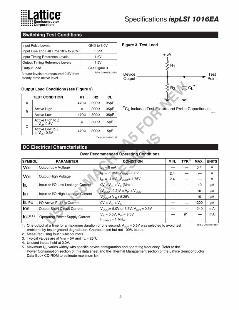
5
Specifications ispLSI 1016EA
USE is
pMACH 4
A5
FOR N
EW
5V D
ESIGNS
Switching Test Conditions
Figure 3. Test Load
DC Electrical Characteristics
Over Recommended Operating Conditions
Input Pulse Levels
Table 2-0003/1016EA
Input Rise and Fall Time 10% to 90%
Input Timing Reference Levels
Output Timing Reference Levels
Output Load
GND to 3.0V
1.5V
1.5ns
1.5V
See Figure 3
3-state levels are measured 0.5V from
steady-state active level.
Output Load Conditions (see Figure 3)
TEST CONDITION R1 R2 CL
A 470Ω 390Ω 35pF
B∞ 390Ω 35pF
470Ω 390Ω 35pF
Active High
Active Low
C
470Ω 390Ω 5pF
∞ 390Ω 5pF
Active Low to Zat V +0.5VOL
Active High to Zat V -0.5VOH
Table 2-0004/1016E
+ 5V
R1
R2 CL*
DeviceOutput
TestPoint
*CL includes Test Fixture and Probe Capacitance.0213a
VOL
SYMBOL
1. One output at a time for a maximum duration of one second. VOUT = 0.5V was selected to avoid test
problems by tester ground degradation. Characterized but not 100% tested.
2. Measured using four 16-bit counters.
3. Typical values are at VCC = 5V and TA = 25°C.
4. Unused inputs held at 0.0V.
5. Maximum ICC varies widely with specific device configuration and operating frequency. Refer to the
Power Consumption section of this data sheet and the Thermal Management section of the Lattice Semiconductor
Data Book CD-ROM to estimate maximum ICC.
Table 2-0007/1016EA
VOH
IIH
IIL
PARAMETER
IIL-PU
IOS1
ICC2, 4, 5
Output Low Voltage
Output High Voltage
Input or I/O Low Leakage Current
Operating Power Supply Current
IOL = 8 mA
0V ≤ VIN ≤ VIL (Max.)
VIL = 0.0V, VIH = 3.0V
CONDITION MIN. TYP.3 MAX. UNITS
—
2.4
—
—
—
—
—
—
—
—
0.4
—
10
-10
10
V
V
2.4 — — V
μAInput or I/O High Leakage Current
VCCIO ≤ VIN ≤ 5.25V
(VCCIO - 0.2)V ≤ VIN ≤ VCCIO
μA
μA
I/O Active Pull-Up Current 0V ≤ VIN ≤ VIL — — -200 μA
Output Short Circuit Current VCCIO = 5.0V or 3.3V, VOUT = 0.5V — — -240 mA
— 91 mA—
fTOGGLE = 1 MHz
IOH = -2 mA, VCCIO = 3.0V
IOH = -4 mA, VCCIO = 4.75V
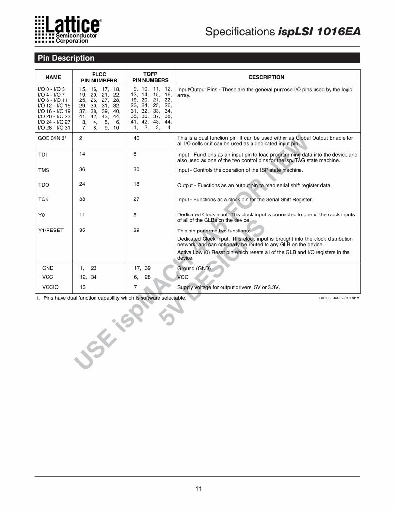
11
Specifications ispLSI 1016EA
USE is
pMACH 4
A5
FOR N
EW
5V D
ESIGNS
This is a dual function pin. It can be used either as Global Output Enable for all I/O cells or it can be used as a dedicated input pin.
Input/Output Pins - These are the general purpose I/O pins used by the logic array.
NAME
Table 2-0002C/1016EA
DESCRIPTION
I/O 0 - I/O 3I/O 4 - I/O 7I/O 8 - I/O 11I/O 12 - I/O 15I/O 16 - I/O 19I/O 20 - I/O 23I/O 24 - I/O 27I/O 28 - I/O 31
GOE 0/IN 31
Y1/RESET1
Y0
TDI
TMS
GND
VCCVCC
Supply voltage for output drivers, 5V or 3.3V.VCCIO
TDO
TCK
Ground (GND)
PLCCPIN NUMBERS
15,19,25,29,37,41, 3, 7,
16,20,26,30,38,42, 4, 8,
17,21,27,31,39,43, 5, 9,
18,22,28,32,40,44, 6,10
2
35
11
14
36
1,
12,
13
24
33
23
34
1. Pins have dual function capability which is software selectable.
TQFPPIN NUMBERS
9,13,19,23,31,35,41, 1,
10,14,20,24,32,36,42, 2,
11,15,21,25,33,37,43, 3,
12,16,22,26,34,38,44, 4
40
29
5
8
30
17,
6,
7
18
27
39
28
Input - Controls the operation of the ISP state machine.
Dedicated Clock input. This clock input is connected to one of the clock inputs of all of the GLBs on the device.
Input - Functions as an input pin to load programming data into the device and also used as one of the two control pins for the ispJTAG state machine.
Output - Functions as an output pin to read serial shift register data.
Input - Functions as a clock pin for the Serial Shift Register.
This pin performs two functions:
Dedicated Clock input. This clock input is brought into the clock distribution network, and can optionally be routed to any GLB on the device.
Active Low (0) Reset pin which resets all of the GLB and I/O registers in the device.
Pin Description
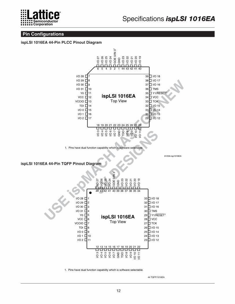
12
Specifications ispLSI 1016EA
USE is
pMACH 4
A5
FOR N
EW
5V D
ESIGNS
I/O 18
I/O 17
I/O 16
TMS
Y1/RESET1
VCC
TCK
I/O 15
I/O 14
I/O 13
I/O 12
I/O 28
I/O 29
I/O 30
I/O 31
Y0
VCC
VCCIO
TDI
I/O 0
I/O 1
I/O 2
I/O
27
I/O
26
I/O
25
I/O
24
GO
E 0
/IN
31
GN
D
I/O
23
I/O
22
I/O
21
I/O
20
I/O
19
I/O
3
I/O
4
I/O
5
I/O
6
I/O
7
GN
D
TD
O
I/O
8
I/O
9
I/O
10
I/O
11
ispLSI 1016EATop View
7
8
9
10
12
11
13
14
15
16
17
39
38
37
36
35
34
33
32
31
30
29
6
18
5
19
4
20
3
21
2
22
1
23
44
24
43
25
42
26
41
27
40
28
0123A-isp1016EA
1. Pins have dual function capability which is software selectable.
ispLSI 1016EA 44-Pin TQFP Pinout Diagram
I/O 18
I/O 17
I/O 16
TMS
Y1/RESET1
VCC
TCK
I/O 15
I/O 14
I/O 13
I/O 12
I/O 28
I/O 29
I/O 30
I/O 31
Y0
VCC
VCCIO
TDI
I/O 0
I/O 1
I/O 2
I/O
27
I/O
26
I/O
25
I/O
24
GO
E 0
/IN
31
GN
D
I/O
23
I/O
22
I/O
21
I/O
20
I/O
19
I/O
3
I/O
4
I/O
5
I/O
6
I/O
7
GN
D
TD
O
I/O
8
I/O
9
I/O
10
I/O
11
ispLSI 1016EATop View
1
2
3
4
6
5
7
8
9
10
11
33
32
31
30
29
28
27
26
25
24
23
44
12
43
13
42
14
41
15
40
16
39
17
38
18
37
19
36
20
35
21
34
22
44 TQFP/1016EA
1. Pins have dual function capability which is software selectable.
Pin Configurations
ispLSI 1016EA 44-Pin PLCC Pinout Diagram