Embed Size (px)
Citation preview
Page 1 of 15
Document No. 70-0245-05 www.psemi.com ©2008-2009 Peregrine Semiconductor Corp. All rights reserved.
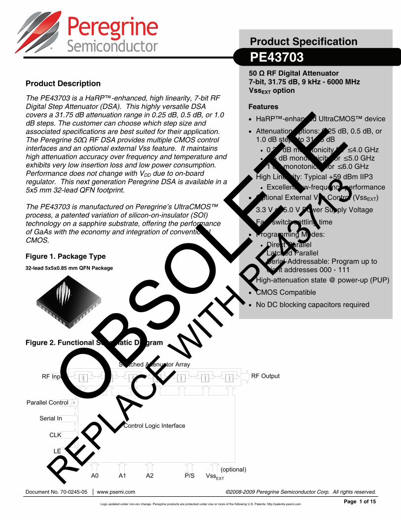
The PE43703 is a HaRP™-enhanced, high linearity, 7-bit RF Digital Step Attenuator (DSA). This highly versatile DSA covers a 31.75 dB attenuation range in 0.25 dB, 0.5 dB, or 1.0 dB steps. The customer can choose which step size and associated specifications are best suited for their application. The Peregrine 50Ω RF DSA provides multiple CMOS control interfaces and an optional external Vss feature. It maintains high attenuation accuracy over frequency and temperature and exhibits very low insertion loss and low power consumption. Performance does not change with VDD due to on-board regulator. This next generation Peregrine DSA is available in a 5x5 mm 32-lead QFN footprint. The PE43703 is manufactured on Peregrine’s UltraCMOS™ process, a patented variation of silicon-on-insulator (SOI) technology on a sapphire substrate, offering the performance of GaAs with the economy and integration of conventional CMOS.
Product Specification
50 Ω RF Digital Attenuator 7-bit, 31.75 dB, 9 kHz - 6000 MHz VssEXT option
Product Description
Figure 2. Functional Schematic Diagram
PE43703
Features
HaRP™-enhanced UltraCMOS™ device
Attenuation options: 0.25 dB, 0.5 dB, or 1.0 dB steps to 31.75 dB 0.25 dB monotonicity for ≤ 4.0 GHz 0.5 dB monotonicity for ≤ 5.0 GHz 1 dB monotonicity for ≤ 6.0 GHz
High Linearity: Typical +59 dBm IIP3 Excellent low-frequency performance
Optional External Vss Control (VssEXT)
3.3 V or 5.0 V Power Supply Voltage
Fast switch settling time
Programming Modes: Direct Parallel Latched Parallel Serial-Addressable: Program up to
eight addresses 000 - 111 High-attenuation state @ power-up (PUP)
CMOS Compatible
No DC blocking capacitors required
Figure 1. Package Type 32-lead 5x5x0.85 mm QFN Package
Control Logic Interface
RF Input RF Output
Switched Attenuator Array
Serial In
LE
CLK
A0 A1 A2
Parallel Control 7
P/S VssEXT
(optional)
OBSOLETE
REPLACE W
ITH PE43
713
Logo updated under non-rev change. Peregrine products are protected under one or more of the following U.S. Patents: http://patents.psemi.com
Product Specification PE43703
Page 2 of 15
©2008-2009 Peregrine Semiconductor Corp. All rights reserved. Document No. 70-0245-05 UltraCMOS™ RFIC Solutions
-1.5
-1.0
-0.5
0.0
0.5
1.0
1.5
0.0 4.0 8.0 12.0 16.0 20.0 24.0 28.0 32.0
Attenuation Setting (dB)
Att
enu
atio
n E
rro
r (d
B)
200 MHz 900 MHz 1800 MHz
2200 MHz 3000 MHz 4000 MHz
-1.5
-1.0
-0.5
0.0
0.5
1.0
1.5
0 1000 2000 3000 4000
Frequency (MHz)
Att
en
ua
tio
n E
rro
r (d
B)
0.25dB State 0.5dB State 1dB State 2dB State4dB State 8dB State 16dB State 31.75dB State
-0.25
0.00
0.25
0.50
0 4 8 12 16 20 24 28 32
Attenuation Setting (dB)
Ste
p A
tten
uatio
n (d
B)
200 MHz 900 MHz 1800 MHz 2200 MHz 3000 MHz
5 10 15 20 25 300 35
5
10
15
20
25
30
0
35
Attenuation State
Atte
nuat
ion
dB
0.25-dB PE43701 Attenuation
900 MHz1800 MHz2200 MHz3000 MHz
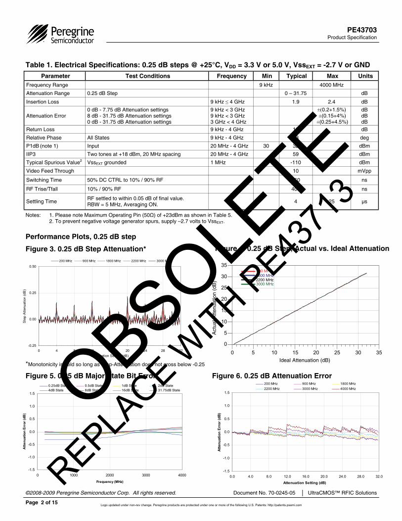
Table 1. Electrical Specifications: 0.25 dB steps @ +25°C, VDD = 3.3 V or 5.0 V, VssEXT = -2.7 V or GND
Notes: 1. Please note Maximum Operating Pin (50Ω) of +23dBm as shown in Table 5. 2. To prevent negative voltage generator spurs, supply –2.7 volts to VssEXT.
Parameter Test Conditions Frequency Min Typical Max Units Frequency Range 9 kHz 4000 MHz
Attenuation Range 0.25 dB Step 0 – 31.75 dB
Insertion Loss 9 kHz ≤ 4 GHz 1.9 2.4 dB
Attenuation Error 0 dB - 7.75 dB Attenuation settings 8 dB - 31.75 dB Attenuation settings 0 dB - 31.75 dB Attenuation settings
9 kHz < 3 GHz 9 kHz < 3 GHz 3 GHz < 4 GHz
±(0.2+1.5%) ±(0.15+4%)
±(0.25+4.5%)
dB dB dB
Return Loss 9 kHz - 4 GHz 18 dB
Relative Phase All States 9 kHz - 4 GHz 33 deg
P1dB (note 1) Input 20 MHz - 4 GHz 30 32 dBm
IIP3 Two tones at +18 dBm, 20 MHz spacing 20 MHz - 4 GHz 59 dBm
Typical Spurious Value2 VssEXT grounded 1 MHz -110 dBm
Video Feed Through 10 mVpp
Switching Time 50% DC CTRL to 10% / 90% RF 650 ns
RF Trise/Tfall 10% / 90% RF 400 ns
Settling Time RF settled to within 0.05 dB of final value. RBW = 5 MHz, Averaging ON. 4 25 µs
*Monotonicity is held so long as Step-Attenuation does not cross below -0.25
Figure 3. 0.25 dB Step Attenuation*
Performance Plots, 0.25 dB step Figure 4. 0.25 dB Step, Actual vs. Ideal Attenuation
Figure 5. 0.25 dB Major State Bit Error Figure 6. 0.25 dB Attenuation Error
Ideal Attenuation (dB)
Act
ual A
ttenu
atio
n (d
B)
OBSOLETE
REPLACE W
ITH PE43
713
Logo updated under non-rev change. Peregrine products are protected under one or more of the following U.S. Patents: http://patents.psemi.com
Product Specification PE43703
Page 3 of 15
Document No. 70-0245-05 www.psemi.com ©2008-2009 Peregrine Semiconductor Corp. All rights reserved.
-0.500
0.000
0.500
1.000
0 4 8 12 16 20 24 28 32
Attenuation Setting (dB)
Ste
p A
tten
uat
ion
(d
B)
200 MHz 900 MHz 1800 MHz 2200 MHz
3000 MHz 4000 MHz 5000 MHz
900 MHz2200 MHz3800 MHz5000 MHz
5 10 15 20 25 300 35
5
10
15
20
25
30
0
35
Attenuation State
Atte
nuat
ion
dB
0.5-dB PE43703 Attenuation
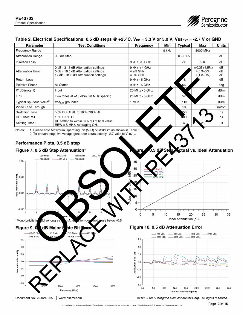
Table 2. Electrical Specifications: 0.5 dB steps @ +25°C, VDD = 3.3 V or 5.0 V, VssEXT = -2.7 V or GND
Figure 7. 0.5 dB Step Attenuation* Performance Plots, 0.5 dB step
Parameter Test Conditions Frequency Min Typical Max Units Frequency Range 9 kHz 5000 MHz
Attenuation Range 0.5 dB Step 0 – 31.5 dB
Insertion Loss 9 kHz ≤ 5 GHz 2.0 2.6 dB
Attenuation Error 0 dB - 31.5 dB Attenuation settings 0 dB - 16.5 dB Attenuation settings 17 dB - 31.5 dB Attenuation settings
9 kHz < 4 GHz 4 ≤ 5 GHz 4 ≤ 5 GHz
±(0.25+4.5%)
±(0.3+5%) ±(1.3+0%)
dB dB dB
Return Loss 9 kHz - 5 GHz 18 dB
Relative Phase All States 9 kHz - 5 GHz 56 deg
P1dB (note 1) Input 20 MHz - 5 GHz 30 32 dBm
IIP3 Two tones at +18 dBm, 20 MHz spacing 20 MHz - 5 GHz 57 dBm
Typical Spurious Value2 VssEXT grounded 1 MHz -110 dBm
Video Feed Through 10 mVpp
Switching Time 50% DC CTRL to 10% / 90% RF 650 ns RF Trise/Tfall 10% / 90% RF 400 ns
Settling Time RF settled to within 0.05 dB of final value. RBW = 5 MHz, Averaging ON. 4 25 µs
*Monotonicity is held so long as Step-Attenuation does not cross below -0.5
Figure 8. 0.5 dB Step, Actual vs. Ideal Attenuation
Figure 9. 0.5 dB Major State Bit Error Figure 10. 0.5 dB Attenuation Error
Ideal Attenuation (dB)
Act
ual A
ttenu
atio
n (d
B)
-1.5
-1.0
-0.5
0.0
0.5
1.0
1.5
0 1000 2000 3000 4000 5000
Frequency (MHz)
Att
enu
atio
n E
rro
r (d
B)
0.5dB State 1dB State 2dB State 4dB State
8dB State 16dB State 31.5dB State
-1.5
-1.0
-0.5
0.0
0.5
1.0
1.5
0.0 4.0 8.0 12.0 16.0 20.0 24.0 28.0 32.0
Attenuation Setting (dB)
Att
enu
atio
n E
rro
r (d
B)
200 MHz 900 MHz 1800 MHz 2200 MHz
3000 MHz 4000 MHz 5000 MHz
Notes: 1. Please note Maximum Operating Pin (50Ω) of +23dBm as shown in Table 5. 2. To prevent negative voltage generator spurs, supply –2.7 volts to VssEXT.
OBSOLETE
REPLACE W
ITH PE43
713
Logo updated under non-rev change. Peregrine products are protected under one or more of the following U.S. Patents: http://patents.psemi.com
Product Specification PE43703
Page 4 of 15
©2008-2009 Peregrine Semiconductor Corp. All rights reserved. Document No. 70-0245-05 UltraCMOS™ RFIC Solutions
-1.5
-1.0
-0.5
0.0
0.5
1.0
1.5
0 4 8 12 16 20 24 28 32
Attenuation Setting (dB)
Att
en
ua
tio
n E
rro
r (d
B)
200 MHz 900 MHz 1800 MHz 2200 MHz
-1.5
-1.0
-0.5
0.0
0.5
1.0
1.5
0 1000 2000 3000 4000 5000 6000
Frequency (MHz)
Bit
Err
or
(dB
)
1dB State 2dB State 4dB State
8dB State 16dB State 31dB State
-1
-0.5
0
0.5
1
0 4 8 12 16 20 24 28 32
Attenuation Setting (dB)
Ste
p A
tten
uat
ion
(d
B)
200 MHz 900 MHz 1800 MHz 2200 MHz3000 MHz 4000 MHz 5000 MHz 6000 MHz
900 MHz2200 MHz3800 MHz5800 MHz
5 10 15 20 25 300 35
5
10
15
20
25
30
0
35
Attenuation State
Atte
nuat
ion
dB
1-dB PE43703 Attenuation
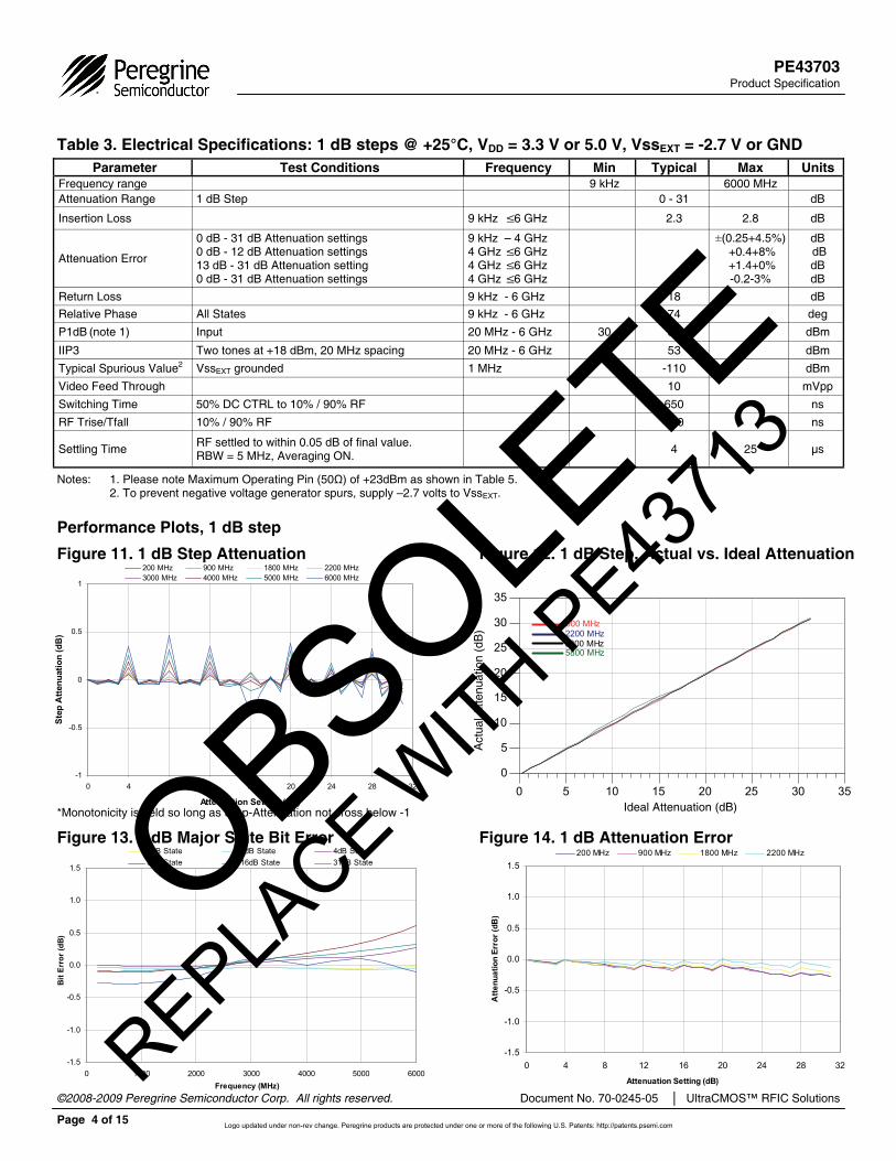
Table 3. Electrical Specifications: 1 dB steps @ +25°C, VDD = 3.3 V or 5.0 V, VssEXT = -2.7 V or GND
Performance Plots, 1 dB step
Parameter Test Conditions Frequency Min Typical Max Units Frequency range 9 kHz 6000 MHz Attenuation Range 1 dB Step 0 - 31 dB
Insertion Loss 9 kHz ≤ 6 GHz 2.3 2.8 dB
Attenuation Error
0 dB - 31 dB Attenuation settings 0 dB - 12 dB Attenuation settings 13 dB - 31 dB Attenuation setting 0 dB - 31 dB Attenuation settings
9 kHz – 4 GHz 4 GHz ≤ 6 GHz 4 GHz ≤ 6 GHz 4 GHz ≤ 6 GHz
±(0.25+4.5%) +0.4+8% +1.4+0% -0.2-3%
dB dB dB dB
Return Loss 9 kHz - 6 GHz 18 dB Relative Phase All States 9 kHz - 6 GHz 74 deg P1dB (note 1) Input 20 MHz - 6 GHz 30 32 dBm
IIP3 Two tones at +18 dBm, 20 MHz spacing 20 MHz - 6 GHz 53 dBm Typical Spurious Value2 VssEXT grounded 1 MHz -110 dBm Video Feed Through 10 mVpp Switching Time 50% DC CTRL to 10% / 90% RF 650 ns RF Trise/Tfall 10% / 90% RF 400 ns
Settling Time RF settled to within 0.05 dB of final value. RBW = 5 MHz, Averaging ON. 4 25 µs
*Monotonicity is held so long as Step-Attenuation not cross below -1
Figure 12. 1 dB Step, Actual vs. Ideal Attenuation Figure 11. 1 dB Step Attenuation
Figure 13. 1 dB Major State Bit Error Figure 14. 1 dB Attenuation Error
Ideal Attenuation (dB)
Act
ual A
ttenu
atio
n (d
B)
Notes: 1. Please note Maximum Operating Pin (50Ω) of +23dBm as shown in Table 5. 2. To prevent negative voltage generator spurs, supply –2.7 volts to VssEXT.
OBSOLETE
REPLACE W
ITH PE43
713
Logo updated under non-rev change. Peregrine products are protected under one or more of the following U.S. Patents: http://patents.psemi.com
Product Specification PE43703
Page 5 of 15
Document No. 70-0245-05 www.psemi.com ©2008-2009 Peregrine Semiconductor Corp. All rights reserved.
-50
-45
-40
-35
-30
-25
-20
-15
-10
-5
0
0 1 2 3 4 5 6 7 8 9
Frequency (GHz)
Re
turn
Lo
ss
(d
B)
-40C 25C 85C
-40
-35
-30
-25
-20
-15
-10
-5
0
0 1 2 3 4 5 6 7 8 9
Frequency (GHz)
Re
turn
Lo
ss
(d
B)
-40C 25C 85C
-60
-50
-40
-30
-20
-10
0
0 1 2 3 4 5 6 7 8 9Frequency (GHz)
Re
turn
Lo
ss
(d
B)
0dB 0.25dB 0.5dB 1dB 2dB4dB 8dB 16dB 31.75dB
-5
-4.5
-4
-3.5
-3
-2.5
-2
-1.5
-1
-0.5
0
0.0 1.0 2.0 3.0 4.0 5.0 6.0 7.0 8.0 9.0
Frequency (GHz)
Inse
rtio
n Lo
ss (
dB)
-40C +25C +85C
-70
-60
-50
-40
-30
-20
-10
0
0 1 2 3 4 5 6 7 8 9
Frequency (GHz)
Re
turn
Lo
ss
(d
B)
0dB 0.25dB 0.5dB 1dB 2dB
4dB 8dB 16dB 31.75dB
-1.5
-1.0
-0.5
0.0
0.5
1.0
1.5
0 4 8 12 16 20 24 28 32
Attenuation Setting (dB)
Att
enu
atio
n E
rro
r (d
B)
3000 MHz 4000 MHz 5000 MHz 6000 MHz
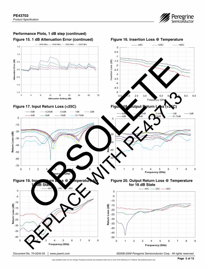
Figure 15. 1 dB Attenuation Error (continued) Figure 16. Insertion Loss @ Temperature Performance Plots, 1 dB step (continued)
Figure 17. Input Return Loss (+25C) Figure 18. Output Return Loss (+25C)
Figure 19. Input Return Loss @ Temperature for 16 dB State
Figure 20. Output Return Loss @ Temperature for 16 dB State
OBSOLETE
REPLACE W
ITH PE43
713
Logo updated under non-rev change. Peregrine products are protected under one or more of the following U.S. Patents: http://patents.psemi.com
Product Specification PE43703
Page 6 of 15
©2008-2009 Peregrine Semiconductor Corp. All rights reserved. Document No. 70-0245-05 UltraCMOS™ RFIC Solutions
30
35
40
45
50
55
60
65
70
0 1000 2000 3000 4000 5000 6000 7000
Frequency (MHz)
Inp
ut I
P3
(d
Bm
)
0dB 0.25dB 0.5dB 1dB 2dB
4dB 8dB 16dB 31.75dB
-1.5
-1.0
-0.5
0.0
0.5
1.0
1.5
0 4 8 12 16 20 24 28 32
Attenuation Setting (dB)
Att
enua
tion
Err
or (
dB)
+25C -40C +85C
-1.5
-1.0
-0.5
0.0
0.5
1.0
1.5
0 4 8 12 16 20 24 28 32
Attenuation Setting (dB)
Att
en
ua
tion
Err
or
(dB
)+25C -40C +85C
-1.5
-1.0
-0.5
0.0
0.5
1.0
1.5
0.0 4.0 8.0 12.0 16.0 20.0 24.0 28.0 32.0
Attenuation Setting (dB)
Atte
nu
atio
n E
rro
r (d
B)
+25 C -40C +85C
0.00
5.00
10.00
15.00
20.00
25.00
30.00
35.00
-40 -20 0 20 40 60 80
Temperature (Deg C)
Ph
ase
(Deg
)
900 MHz 1800 MHz 3000 MHz
0
20
40
60
80
100
120
0 1 2 3 4 5 6 7 8Frequency (GHz)
Re
lativ
e P
ha
se E
rro
r (D
eg)
0dB 0.25dB 0.5dB 1dB 2dB
4dB 8dB 16dB 31.75dB
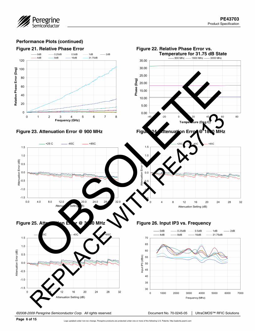
Figure 21. Relative Phase Error Figure 22. Relative Phase Error vs. Temperature for 31.75 dB State
Performance Plots (continued)
Figure 23. Attenuation Error @ 900 MHz Figure 24. Attenuation Error @ 1800 MHz
Figure 25. Attenuation Error @ 3000 MHz Figure 26. Input IP3 vs. Frequency
OBSOLETE
REPLACE W
ITH PE43
713
Logo updated under non-rev change. Peregrine products are protected under one or more of the following U.S. Patents: http://patents.psemi.com
Product Specification PE43703
Page 7 of 15
Document No. 70-0245-05 www.psemi.com ©2008-2009 Peregrine Semiconductor Corp. All rights reserved.
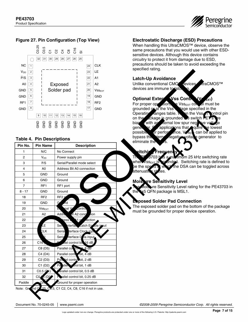
Electrostatic Discharge (ESD) Precautions When handling this UltraCMOS™ device, observe the same precautions that you would use with other ESD-sensitive devices. Although this device contains circuitry to protect it from damage due to ESD, precautions should be taken to avoid exceeding the specified rating.
Exposed Solder Pad Connection The exposed solder pad on the bottom of the package must be grounded for proper device operation.
Figure 27. Pin Configuration (Top View)
Latch-Up Avoidance Unlike conventional CMOS devices, UltraCMOS™ devices are immune to latch-up.
Switching Frequency The PE43703 has a maximum 25 kHz switching rate when VssEXT is grounded. Switching rate is defined to be the speed at which the DSA can be toggled across attenuation states.
Pin No. Pin Name Description 1 N/C No Connect
2 VDD Power supply pin
3 P/S Serial/Parallel mode select
4 A0 Address Bit A0 connection
5 GND Ground
6 GND Ground
7 RF1 RF1 port
8 - 17 GND Ground
18 RF2 RF2 port
19 GND Ground
20 VssEXT External Vss Control
21 A2 Address Bit A2 connection
22 A1 Address Bit A1 connection
23 LE Serial interface Latch Enable input
24 CLK Serial interface Clock input
25 SI Serial interface Data input
26 C16 (D6) Parallel control bit, 16 dB
27 C8 (D5) Parallel control bit, 8 dB
28 C4 (D4) Parallel control bit, 4 dB
29 C2 (D3) Parallel control bit, 2 dB
30 C1 (D2) Parallel control bit, 1 dB
31 C0.5 (D1) Parallel control bit, 0.5 dB
32 C0.25 (D0) Parallel control bit, 0.25 dB
Paddle GND Ground for proper operation
8
7
6
5
4
3
2
1 24
23
22
21
20
19
18
17
32 31 30 29 28 27 26 25
161514131211109
ExposedSolder pad
NC
VDD
P/S
A0
GND
GND
RF1
GND
GN
D
GN
D
GN
D
GN
D
GN
D
GN
D
GN
D
GN
D
CLK
LE
A1
A2
VssEXT
GND
RF2
GND
C0.
25
C0.
5
C1
C2
C4
C8
C16
SI
Optional External Vss Control (VssEXT) For proper operation, the VssEXT control must be grounded or at the Vss voltage specified in the Operating Ranges table. When the VssEXT control pin on the package is grounded the switch FET’s are biased with an internal low spur negative voltage generator. For applications that require the lowest possible spur performance, VssEXT can be applied to bypass the internal negative voltage generator to eliminate the spurs. Table 4. Pin Descriptions
Moisture Sensitivity Level The Moisture Sensitivity Level rating for the PE43703 in the 5x5 QFN package is MSL1.
Note: Ground C0.25, C0.5, C1 C2, C4, C8, C16 if not in use.
OBSOLETE
REPLACE W
ITH PE43
713
Logo updated under non-rev change. Peregrine products are protected under one or more of the following U.S. Patents: http://patents.psemi.com
Product Specification PE43703
Page 8 of 15
©2008-2009 Peregrine Semiconductor Corp. All rights reserved. Document No. 70-0245-05 UltraCMOS™ RFIC Solutions
0.0
5.0
10.0
15.0
20.0
25.0
30.0
1.0E+03 1.0E+04 1.0E+05 1.0E+06 1.0E+07 1.0E+08 1.0E+09
Hz
Pin
dB
m
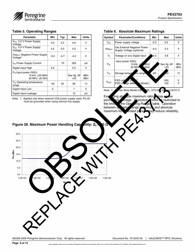
Note: 1. Applied only when external VSS power supply used. Pin 20 must be grounded when using internal Vss supply
Table 5. Operating Ranges Table 6. Absolute Maximum Ratings Parameter Min Typ Max Units
VDD 3.3 V Power Supply Voltage 3.0 3.3 3.6 V
VDD 5.0 V Power Supply Voltage 4.5 5.0 5.5 V
VssEXT Negative Power Supply Voltage1 -3.0 -2.7 -2.4 V
IDD Power Supply Current 70 350 μA
Digital Input High 2.6 5.5 V
PIN Input power (50Ω): 9 kHz ≤ 20 MHz
20 MHz ≤ 6 GHz
See fig. 28
+23
dBm dBm
TOP Operating temperature range -40 25 85 °C
Digital Input Low 0 1 V
Digital Input Leakage 15 μA
Symbol Parameter/Conditions Min Max Units
VDD Power supply voltage -0.3 6.0 V
VssEXT Vss External Negative Power Supply Voltage (optional) -4.0 0.3 V
VI Voltage on any Digital input -0.3 5.8 V
TST Storage temperature range -65 150 °C
VESD ESD voltage (HBM)1 ESD voltage (Machine Model) 500
100 V V
PIN Input power (50Ω)
9 kHz ≤ 20 MHz 20 MHz ≤ 6 GHz
See fig. 28 +23
dBm dBm
Figure 28. Maximum Power Handling Capability: Z0 = 50 Ω
Exceeding absolute maximum ratings may cause permanent damage. Operation should be restricted to the limits in the Operating Ranges table. Operation between operating range maximum and absolute maximum for extended periods may reduce reliability.
Note: 1. Human Body Model (HBM, MIL_STD 883 Method 3015.7)
OBSOLETE
REPLACE W
ITH PE43
713
Logo updated under non-rev change. Peregrine products are protected under one or more of the following U.S. Patents: http://patents.psemi.com
Product Specification PE43703
Page 9 of 15
Document No. 70-0245-05 www.psemi.com ©2008-2009 Peregrine Semiconductor Corp. All rights reserved.
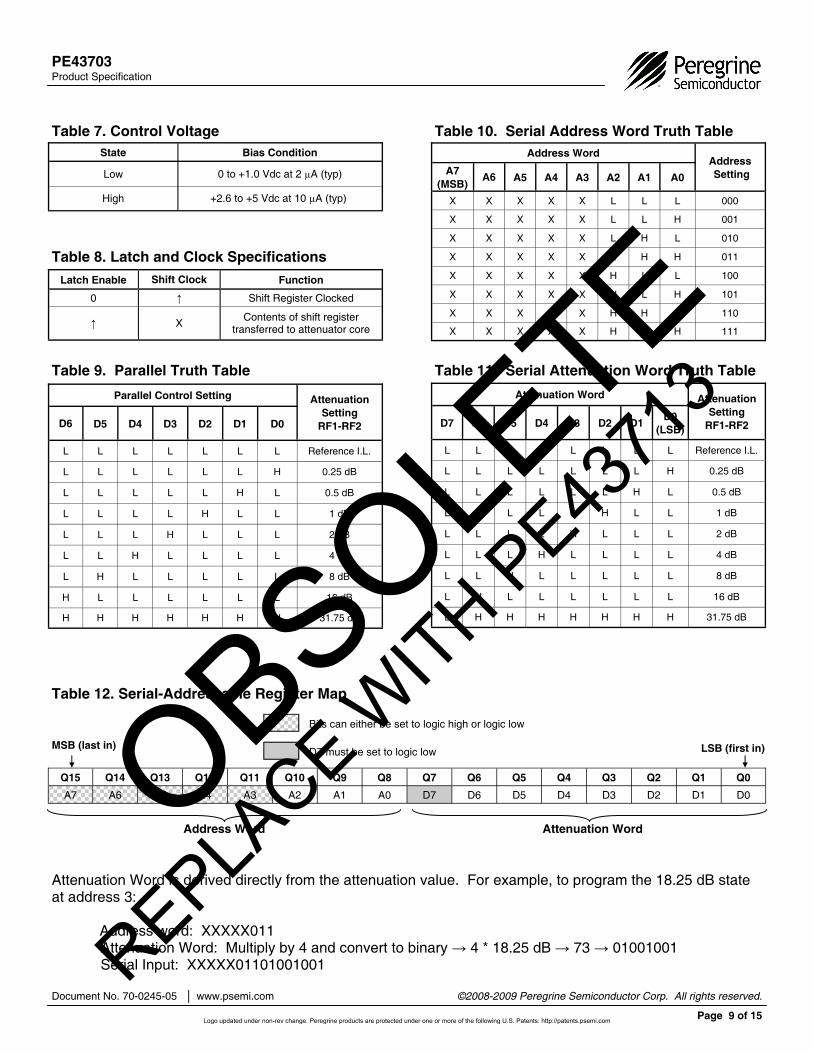
Table 8. Latch and Clock Specifications Latch Enable Function
0 Shift Register Clocked
↑ Contents of shift register transferred to attenuator core
Shift Clock
↑
X
Attenuation Word
D7 D6 D5 D4 D3 D2 D1 D0 (LSB)
L L L L L L L L Reference I.L.
L L L L L L L H 0.25 dB
L L L L L H L L 1 dB
L L L L H L L L 2 dB
L L L H L L L L 4 dB
L L H L L L L L 8 dB
L H L L L L L L 16 dB
L H H H H H H H 31.75 dB
Attenuation Setting
RF1-RF2
L L L L L L H L 0.5 dB
Table 11. Serial Attenuation Word Truth Table
Address Word Address Setting A7
(MSB) A6 A5 A4 A3 A2 A1 A0
X X X X X L L L 000
X X X X X L L H 001
X X X X X L H L 010
X X X X X L H H 011
X X X X X H L L 100
X X X X X H L H 101
X X X X X H H L 110
X X X X X H H H 111
Table 10. Serial Address Word Truth Table Table 7. Control Voltage State Bias Condition
Low 0 to +1.0 Vdc at 2 µA (typ)
High +2.6 to +5 Vdc at 10 µA (typ)
Parallel Control Setting Attenuation Setting
RF1-RF2 D6 D5 D4 D3 D2 D1 D0
L L L L L L L Reference I.L.
L L L L L L H 0.25 dB
L L L L L H L 0.5 dB
L L L L H L L 1 dB
L L L H L L L 2 dB
L L H L L L L 4 dB
L H L L L L L 8 dB
H L L L L L L 16 dB
H H H H H H H 31.75 dB
Table 9. Parallel Truth Table
Table 12. Serial-Addressable Register Map
Q15 Q14 Q13 Q12 Q11 Q10 A7 A6 A5 A4 A3 A2
Q9 Q8 Q7 Q6 Q5 Q4 A1 A0 D7 D6 D5 D4
Q3 Q2 Q1 Q0 D3 D2 D1 D0
Address Word Attenuation Word
LSB (first in) MSB (last in)
Bits can either be set to logic high or logic low
Attenuation Word is derived directly from the attenuation value. For example, to program the 18.25 dB state at address 3: Address word: XXXXX011 Attenuation Word: Multiply by 4 and convert to binary → 4 * 18.25 dB → 73 → 01001001 Serial Input: XXXXX01101001001
D7 must be set to logic low OBSOLETE
REPLACE W
ITH PE43
713
Logo updated under non-rev change. Peregrine products are protected under one or more of the following U.S. Patents: http://patents.psemi.com
Product Specification PE43703
Page 10 of 15
©2008-2009 Peregrine Semiconductor Corp. All rights reserved. Document No. 70-0245-05 UltraCMOS™ RFIC Solutions
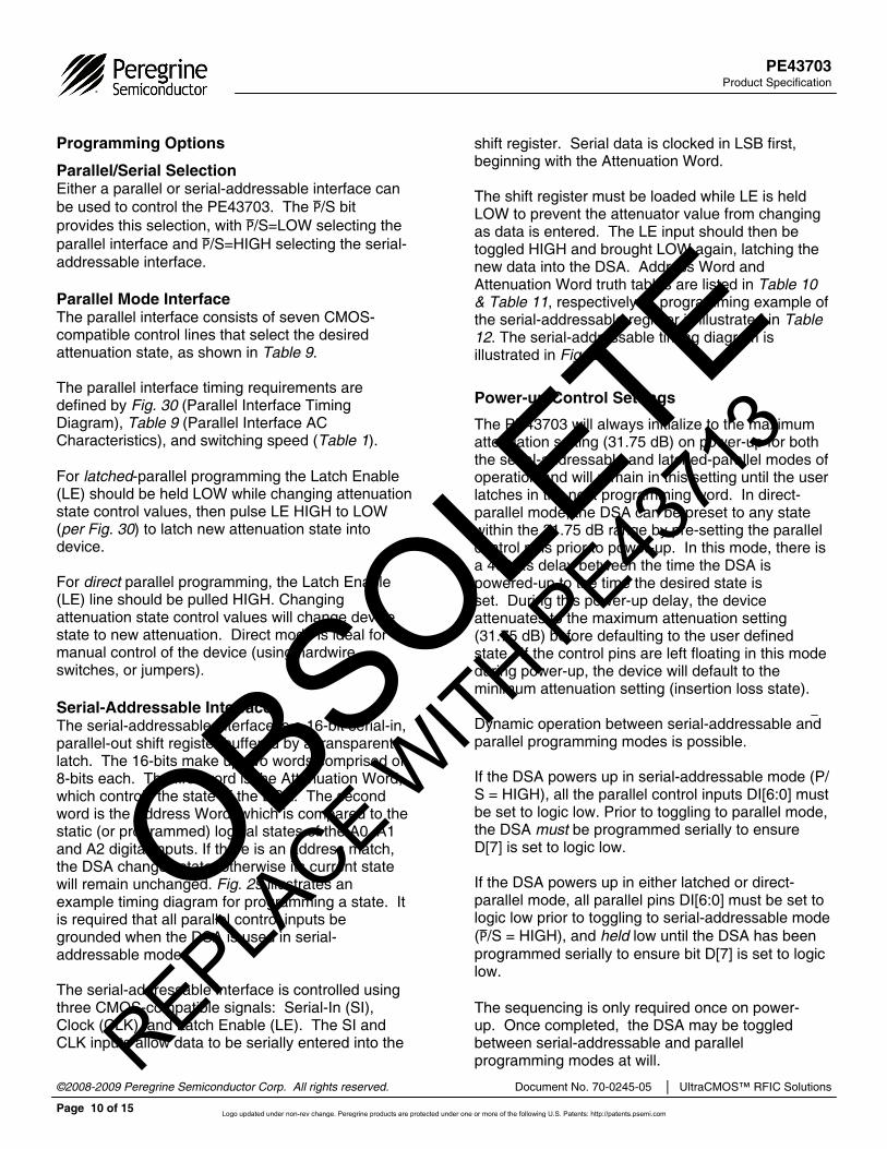
Programming Options
Parallel/Serial Selection Either a parallel or serial-addressable interface can be used to control the PE43703. The P/S bit provides this selection, with P/S=LOW selecting the parallel interface and P/S=HIGH selecting the serial-addressable interface. Parallel Mode Interface The parallel interface consists of seven CMOS-compatible control lines that select the desired attenuation state, as shown in Table 9. The parallel interface timing requirements are defined by Fig. 30 (Parallel Interface Timing Diagram), Table 9 (Parallel Interface AC Characteristics), and switching speed (Table 1). For latched-parallel programming the Latch Enable (LE) should be held LOW while changing attenuation state control values, then pulse LE HIGH to LOW (per Fig. 30) to latch new attenuation state into device. For direct parallel programming, the Latch Enable (LE) line should be pulled HIGH. Changing attenuation state control values will change device state to new attenuation. Direct mode is ideal for manual control of the device (using hardwire, switches, or jumpers). Serial-Addressable Interface The serial-addressable interface is a 16-bit serial-in, parallel-out shift register buffered by a transparent latch. The 16-bits make up two words comprised of 8-bits each. The first word is the Attenuation Word, which controls the state of the DSA. The second word is the Address Word, which is compared to the static (or programmed) logical states of the A0, A1 and A2 digital inputs. If there is an address match, the DSA changes state; otherwise its current state will remain unchanged. Fig. 29 illustrates an example timing diagram for programming a state. It is required that all parallel control inputs be grounded when the DSA is used in serial-addressable mode. The serial-addressable interface is controlled using three CMOS-compatible signals: Serial-In (SI), Clock (CLK), and Latch Enable (LE). The SI and CLK inputs allow data to be serially entered into the
shift register. Serial data is clocked in LSB first, beginning with the Attenuation Word. The shift register must be loaded while LE is held LOW to prevent the attenuator value from changing as data is entered. The LE input should then be toggled HIGH and brought LOW again, latching the new data into the DSA. Address Word and Attenuation Word truth tables are listed in Table 10 & Table 11, respectively. A programming example of the serial-addressable register is illustrated in Table 12. The serial-addressable timing diagram is illustrated in Fig. 29.
Power-up Control Settings
The PE43703 will always initialize to the maximum attenuation setting (31.75 dB) on power-up for both the serial-addressable and latched-parallel modes of operation and will remain in this setting until the user latches in the next programming word. In direct-parallel mode, the DSA can be preset to any state within the 31.75 dB range by pre-setting the parallel control pins prior to power-up. In this mode, there is a 400-µs delay between the time the DSA is powered-up to the time the desired state is set. During this power-up delay, the device attenuates to the maximum attenuation setting (31.75 dB) before defaulting to the user defined state. If the control pins are left floating in this mode during power-up, the device will default to the minimum attenuation setting (insertion loss state). Dynamic operation between serial-addressable and parallel programming modes is possible. If the DSA powers up in serial-addressable mode (P/S = HIGH), all the parallel control inputs DI[6:0] must be set to logic low. Prior to toggling to parallel mode, the DSA must be programmed serially to ensure D[7] is set to logic low. If the DSA powers up in either latched or direct-parallel mode, all parallel pins DI[6:0] must be set to logic low prior to toggling to serial-addressable mode (P/S = HIGH), and held low until the DSA has been programmed serially to ensure bit D[7] is set to logic low. The sequencing is only required once on power-up. Once completed, the DSA may be toggled between serial-addressable and parallel programming modes at will.
OBSOLETE
REPLACE W
ITH PE43
713
Logo updated under non-rev change. Peregrine products are protected under one or more of the following U.S. Patents: http://patents.psemi.com
Product Specification PE43703
Page 11 of 15
Document No. 70-0245-05 www.psemi.com ©2008-2009 Peregrine Semiconductor Corp. All rights reserved.
VDD = 3.3 or 5.0 V, -40° C < TA < 85° C, unless otherwise specified VDD = 3.3 or 5.0 V, -40° C < TA < 85° C, unless otherwise specified
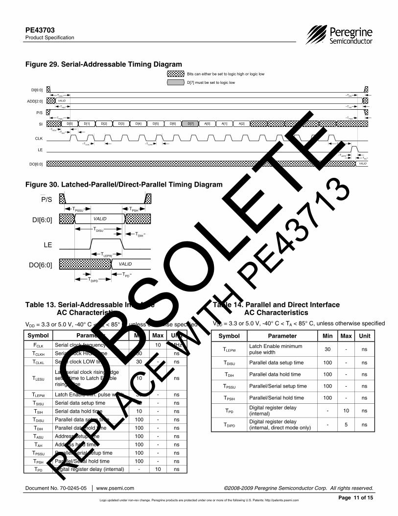
Figure 29. Serial-Addressable Timing Diagram
Figure 30. Latched-Parallel/Direct-Parallel Timing Diagram
Symbol Parameter Min Max Unit FCLK Serial clock frequency - 10 MHz
TCLKH Serial clock HIGH time 30 - ns
TCLKL Serial clock LOW time 30 - ns
TLESU Last serial clock rising edge setup time to Latch Enable rising edge
10 - ns
TLEPW Latch Enable min. pulse width 30 - ns
TSISU Serial data setup time 10 - ns
TSIH Serial data hold time 10 - ns
TDISU Parallel data setup time 100 - ns
TDIH Parallel data hold time 100 - ns
TASU Address setup time 100 - ns
TAH Address hold time 100 - ns
TPSSU Parallel/Serial setup time 100 - ns
TPSH Parallel/Serial hold time 100 - ns TPD Digital register delay (internal) - 10 ns
Symbol Parameter Min Max Unit
TLEPW Latch Enable minimum pulse width 30 - ns
TDISU Parallel data setup time 100 - ns
TDIH Parallel data hold time 100 - ns
TPSSU Parallel/Serial setup time 100 - ns
TPSIH Parallel/Serial hold time 100 - ns
TPD Digital register delay (internal) - 10 ns
TDIPD Digital register delay (internal, direct mode only) - 5 ns
VALID
TDISUTDIH
DI[6:0]
LE
P/STPSSU TPSH
TLEPW
VALIDDO[6:0]
TDIPD
TPD
Table 14. Parallel and Direct Interface AC Characteristics
Table 13. Serial-Addressable Interface AC Characteristics
A[2]A[1]A[0]
TSISU
TCLKL
TLEPW
TSIH
TCLKH
SI
CLK
LE
P/S
TLESU
TPSSU TPSIH
VALID
TASU
ADD[2:0]TAIH
DO[6:0] VALID
DI[6:0]
TPD
TDISU TDIH
D[6]D[5]D[4]D[3]D[2]D[1]D[0] D[7]
D[7] must be set to logic low
Bits can either be set to logic high or logic low
OBSOLETE
REPLACE W
ITH PE43
713
Logo updated under non-rev change. Peregrine products are protected under one or more of the following U.S. Patents: http://patents.psemi.com
Product Specification PE43703
Page 12 of 15
©2008-2009 Peregrine Semiconductor Corp. All rights reserved. Document No. 70-0245-05 UltraCMOS™ RFIC Solutions
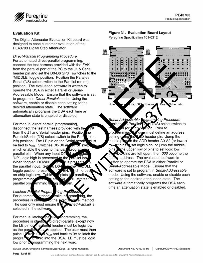
Evaluation Kit The Digital Attenuator Evaluation Kit board was designed to ease customer evaluation of the PE43703 Digital Step Attenuator. Direct-Parallel Programming Procedure For automated direct-parallel programming, connect the test harness provided with the EVK from the parallel port of the PC to the J1 & Serial header pin and set the D0-D6 SP3T switches to the ‘MIDDLE’ toggle position. Position the Parallel/Serial (P/S) select switch to the Parallel (or left) position. The evaluation software is written to operate the DSA in either Parallel or Serial-Addressable Mode. Ensure that the software is set to program in Direct-Parallel mode. Using the software, enable or disable each setting to the desired attenuation state. The software automatically programs the DSA each time an attenuation state is enabled or disabled. For manual direct-parallel programming, disconnect the test harness provided with the EVK from the J1 and Serial header pins. Position the Parallel/Serial (P/S) select switch to the Parallel (or left) position. The LE pin on the Serial header must be tied to VDD. Switches D0-D6 are SP3T switches which enable the user to manually program the parallel bits. When any input D0-D6 is toggled ‘UP’, logic high is presented to the parallel input. When toggled ‘DOWN’, logic low is presented to the parallel input. Setting D0-D6 to the ‘MIDDLE’ toggle position presents an OPEN, which forces an on-chip logic low. Table 9 depicts the parallel programming truth table and Fig. 30 illustrates the parallel programming timing diagram. Latched-Parallel Programming Procedure For automated latched-parallel programming, the procedure is identical to the direct-parallel method. The user only must ensure that Latched-Parallel is selected in the software. For manual latched-parallel programming, the procedure is identical to direct-parallel except now the LE pin on the Serial header must be logic low as the parallel bits are applied. The user must then pulse LE from 0V to VDD and back to 0V to latch the programming word into the DSA. LE must be logic low prior to programming the next word.
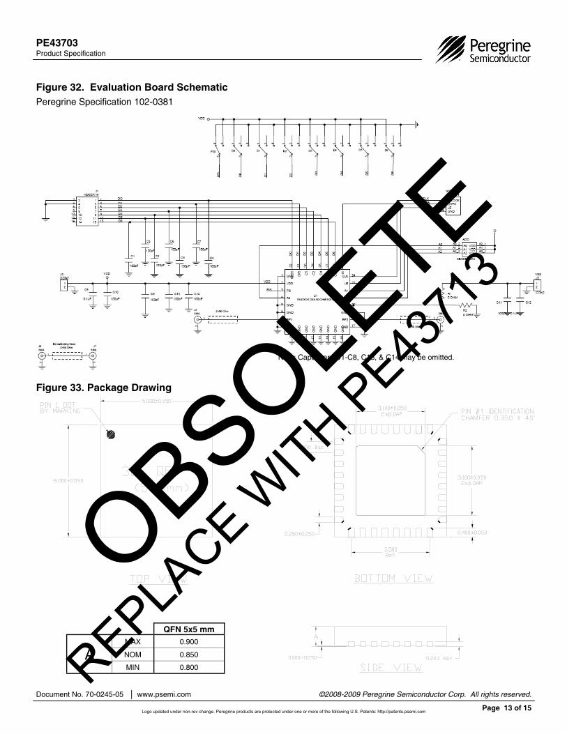
Figure 31. Evaluation Board Layout Peregrine Specification 101-0312
Serial-Addressable Programming Procedure Position the Parallel/Serial (P/S) select switch to the Serial (or right) position. Prior to programming, the user must define an address setting using the ADD header pin. Jump the middle pins on the ADD header A0-A2 (or lower) row of pins to set logic high, or jump the middle pins to the upper row of pins to set logic low. If the ADD pins are left open, then 000 become the default address. The evaluation software is written to operate the DSA in either Parallel or Serial-Addressable Mode. Ensure that the software is set to program in Serial-Addressable mode. Using the software, enable or disable each setting to the desired attenuation state. The software automatically programs the DSA each time an attenuation state is enabled or disabled.
Note: Reference Fig. 32 for Evaluation Board Schematic
OBSOLETE
REPLACE W
ITH PE43
713
Logo updated under non-rev change. Peregrine products are protected under one or more of the following U.S. Patents: http://patents.psemi.com
Product Specification PE43703
Page 13 of 15
Document No. 70-0245-05 www.psemi.com ©2008-2009 Peregrine Semiconductor Corp. All rights reserved.
Figure 33. Package Drawing
QFN 5x5 mm
A MAX 0.900
NOM 0.850
MIN 0.800
Figure 32. Evaluation Board Schematic Peregrine Specification 102-0381
Note: Capacitors C1-C8, C13, & C14 may be omitted.
OBSOLETE
REPLACE W
ITH PE43
713
Logo updated under non-rev change. Peregrine products are protected under one or more of the following U.S. Patents: http://patents.psemi.com
Product Specification PE43703
Page 14 of 15
©2008-2009 Peregrine Semiconductor Corp. All rights reserved. Document No. 70-0245-05 UltraCMOS™ RFIC Solutions
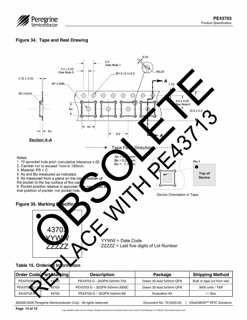
Table 15. Ordering Information
Figure 34. Tape and Reel Drawing
Order Code Part Marking Description Package Shipping Method PE43703MLI 43703 PE43703 G - 32QFN 5x5mm-75A Green 32-lead 5x5mm QFN Bulk or tape cut from reel
PE43703MLI-Z 43703 PE43703 G – 32QFN 5x5mm-3000C Green 32-lead 5x5mm QFN 3000 units / T&R
EK43703-01 43703 PE43703 G – 32QFN 5x5mm-EK Evaluation Kit 1 / Box
Figure 35. Marking Specifications
43703 YYWW ZZZZZ
YYWW = Date Code ZZZZZ = Last five digits of Lot Number
Device Orientation in Tape
Top ofDevice
Pin 1
Tape Feed Direction
OBSOLETE
REPLACE W
ITH PE43
713
Logo updated under non-rev change. Peregrine products are protected under one or more of the following U.S. Patents: http://patents.psemi.com
Product Specification PE43703
Page 15 of 15
Document No. 70-0245-05 www.psemi.com ©2008-2009 Peregrine Semiconductor Corp. All rights reserved.
Sales Offices
The Americas
Peregrine Semiconductor Corporation 9380 Carroll Park Drive San Diego, CA 92121 Tel: 858-731-9400 Fax: 858-731-9499
Europe Peregrine Semiconductor Europe
Bâtiment Maine 13-15 rue des Quatre Vents F-92380 Garches, France Tel: +33-1-4741-9173 Fax : +33-1-4741-9173
For a list of representatives in your area, please refer to our Web site at: www.psemi.com
Data Sheet Identification
Advance Information
The product is in a formative or design stage. The data sheet contains design target specifications for product development. Specifications and features may change in any manner without notice. Preliminary Specification
The data sheet contains preliminary data. Additional data may be added at a later date. Peregrine reserves the right to change specifications at any time without notice in order to supply the best possible product.
Product Specification
The data sheet contains final data. In the event Peregrine decides to change the specifications, Peregrine will notify customers of the intended changes by issuing a CNF (Customer Notification Form).
The information in this data sheet is believed to be reliable. However, Peregrine assumes no liability for the use of this information. Use shall be entirely at the user’s own risk. No patent rights or licenses to any circuits described in this data sheet are implied or granted to any third party. Peregrine’s products are not designed or intended for use in devices or systems intended for surgical implant, or in other applications intended to support or sustain life, or in any application in which the failure of the Peregrine product could create a situation in which personal injury or death might occur. Peregrine assumes no liability for damages, including consequential or incidental damages, arising out of the use of its products in such applications. The Peregrine name, logo, and UTSi are registered trademarks and UltraCMOS, HaRP, MultiSwitch and DuNE are trademarks of Peregrine Semiconductor Corp.
High-Reliability and Defense Products Americas San Diego, CA, USA Phone: 858-731-9475 Fax: 848-731-9499 Europe/Asia-Pacific Aix-En-Provence Cedex 3, France Phone: +33-4-4239-3361 Fax: +33-4-4239-7227
Peregrine Semiconductor, Asia Pacific (APAC) Shanghai, 200040, P.R. China Tel: +86-21-5836-8276 Fax: +86-21-5836-7652 Peregrine Semiconductor, Korea #B-2607, Kolon Tripolis, 210 Geumgok-dong, Bundang-gu, Seongnam-si Gyeonggi-do, 463-943 South Korea Tel: +82-31-728-3939 Fax: +82-31-728-3940 Peregrine Semiconductor K.K., Japan Teikoku Hotel Tower 10B-6 1-1-1 Uchisaiwai-cho, Chiyoda-ku Tokyo 100-0011 Japan Tel: +81-3-3502-5211 Fax: +81-3-3502-5213
OBSOLETE
REPLACE W
ITH PE43
713
Logo updated under non-rev change. Peregrine products are protected under one or more of the following U.S. Patents: http://patents.psemi.com


![R R 34 0.25 0.25 0.25 0.25 0.25 0.25 0.25 0.25 0.25 u 0 25 1 2 3 4 12000C 63kbar 5 k bar ) RR34 0.25 Ö0.25 0.25 0.25 0.25 ú0.75 Q] 0.5 Ö0.5 Ó0.5 Ù0.25 0.25 Ö0](https://img.dokumen.tips/doc/110x75/5e7e08fd2ef2a45bbd70f7b6/r-r-34-025-025-025-025-025-025-025-025-025-u-0-25-1-2-3-4-12000c-63kbar.jpg)


![New Chapter 2 Physical and Link Layer - DISCO · 2020. 8. 31. · Distributed Computing Group MOBILE COMPUTING R. Wattenhofer 2/12 Attenuation by distance • Attenuation [dB] = 10](https://img.dokumen.tips/doc/110x75/6054ad1cbb89a45c641a69db/new-chapter-2-physical-and-link-layer-disco-2020-8-31-distributed-computing.jpg)


