Embed Size (px)
Citation preview

Let's create a pure fiberland for human beings
Fiberland Technology Co.,Ltd
Product Specification
40Gb/s 10km QSFP+ LR4 Transceiver
PRODUCT FEATURES
4 CWDM lanes Mux/Demux design
Up to 11.1Gbps Data rate per wavelength
Up to 10km transmission on SMF
Electrically hot-pluggable
Digital Diagnostics Monitoring Interface
Compliant with QSFP+ MSA with LC connector
Case operating temperature range:0°C to 70°C
Power dissipation < 3.5 W
APPLICATIONS
40G Ethernet
Data Center and LAN
STANDARD
Compliant to IEEE 802.3ba
Compliant to SFF-8436
RoHS Compliant.
Let's create a pure fiberland for human beings
Fiberland Technology Co.,Ltd
General Description
FLD-QSFP+LR4 is designed to operate over single-mode fiber system using 4X10 CWDM channel in
1310 band and links up to 10km. The module converts 4 inputs channel of 10Gb/s electrical data to 4
CWDM optical signals, and multiplexes them into a single channel for 40Gb/s optical transmission.
Reversely, on the receiver side, the module optically de-multiplexes a 40Gb/s input into 4 CWDM
channels signals, and converts them to 4 channel output electrical data.
The central wavelengths of the 4 CWDM channels are 1271, 1291, 1311 and 1331 nm. It contains a
duplex LC connector for the optical interface and a 38-pin connector for the electrical interface. Single-
mode fiber (SMF) is applied in this module. This product converts the 4-channel 10Gb/s electrical input
data into CWDM optical signals (light), by a 4-wavelength Distributed Feedback Laser (DFB) array. The
4 wavelengths are multiplexed into a single 40Gb/s data, propagating out of the transmitter module via
the SMF. The receiver module accepts the 40Gb/s optical signals input, and de-multiplexes it into 4
CWDM 10Gb/s channels. Each wavelength light is collected by a discrete photo diode, and then
outputted as electric data after amplified by a TIA.
The product is designed with form factor, optical/electrical connection and digital diagnostic interface
according to the QSFP+ Multi-Source Agreement (MSA) and compliant to 40G QSFP+ LR4 of IEEE
802.3ba.
Ⅰ Absolute Maximum Ratings
Parameter Symbol Min. Typ. Max. Unit NoteStorage Temperature Ts -40 - 85 ºC
Storage Ambient Humidity HA 5 - 95 %Operating Relative Humidity RH - - 85 %
Power Supply Voltage VCC -0.3 - 4 VSignal Input Voltage Vcc-0.3 - Vcc+0.3 V
Let's create a pure fiberland for human beings
Fiberland Technology Co.,Ltd
Ⅱ Recommended Operating ConditionsParameter Symbol Min. Typ. Max. Unit Note
Case Operating Temperature Tcase 0 - 70 ºC Without air flowPower Supply Voltage VCC 3.14 3.3 3.47 VPower Supply Current ICC - 800 mA
Data Rate BR 10.3125 Gbps Each channelTransmission Distance TD - 10 km
Coupled fiber Single mode fiber 9/125um SMF
Ⅲ Optical Characteristics
Parameter Symbol Min Typ Max Unit NOTE
Transmitter
λ0 1264.5 1271 1277.5 nm
λ1 1284.5 1291 1297.5 nm
λ2 1304.5 1311 1317.5 nmWavelength Assignment
λ3 1324.5 1331 1337.5 nm
Total Output. Power POUT 8.3 dBm
Average Launch Power Per lane -7 2.3 dBm
Spectral Width (-20dB) σ 1 nm
SMSR 30 dB
Optical Extinction Ratio ER 3.5 dB
Average launch Power off per lane Poff -30 dBm
Transmitter and Dispersion Peanlty TDP 2.3 dB
RIN RIN -128 dB/Hz
Output Eye Mask Compliant with IEEE 802.3ba
Receiver
Rx Sensitivity per lane(OMA) RSENS -11.5 dBm 1
Input Saturation Power (Overload) Psat 3.3 dBm
Receiver Reflectance Rr -26 dB
Notes:
1. Measured with a PRBS 231
-1 test pattern, @10.325Gb/s, BER<10-12
.
Let's create a pure fiberland for human beings
Fiberland Technology Co.,Ltd
IV. Electrical Characteristics
Parameter Symbol Min Typ Max Unit NOTE
Supply Voltage Vcc 3.14 3.3 3.46 V
Supply Current Icc 760 mA
Transmitter
Input differential impedance Rin 100 Ω 1
Differential data input swing Vin,pp 180 1000 mV
Transmit Disable Voltage VD Vcc–1.3 Vcc V
Transmit Enable Voltage VEN Vee Vee+ 0.8 V 2
Transmit Disable Assert Time 10 us
Receiver
Differential data output swing Vout,pp 300 850 mV 3
Data output rise time tr 28 ps 4
Data output fall time tf 28 ps 4
LOS Fault VLOS fault Vcc–1.3 VccHOST V 5
LOS Normal VLOS norm Vee Vee+0.8 V 5
Power Supply Rejection PSR 100 mVpp 6
Notes:
1. Connected directly to TX data input pins. AC coupled thereafter.
2. Or open circuit.
3. Into 100 ohms differential termination.
4. 20 – 80 %.
5. Loss Of Signal is LVTTL. Logic 0 indicates normal operation; logic 1 indicates no signal detected.
6. Receiver sensitivity is compliant with power supply sinusoidal modulation of 20 Hz to 1.5 MHz up to specified
value applied through the recommended power supply filtering network.
Let's create a pure fiberland for human beings
Fiberland Technology Co.,Ltd
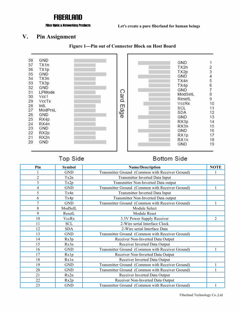
V. Pin AssignmentFigure 1---Pin out of Connector Block on Host Board
Pin Symbol Name/Description NOTE1 GND Transmitter Ground (Common with Receiver Ground) 12 Tx2n Transmitter Inverted Data Input3 Tx2p Transmitter Non-Inverted Data output4 GND Transmitter Ground (Common with Receiver Ground) 15 Tx4n Transmitter Inverted Data Input6 Tx4p Transmitter Non-Inverted Data output7 GND Transmitter Ground (Common with Receiver Ground) 18 ModSelL Module Select9 ResetL Module Reset10 VccRx 3.3V Power Supply Receiver 211 SCL 2-Wire serial Interface Clock12 SDA 2-Wire serial Interface Data13 GND Transmitter Ground (Common with Receiver Ground)14 Rx3p Receiver Non-Inverted Data Output 15 Rx3n Receiver Inverted Data Output16 GND Transmitter Ground (Common with Receiver Ground) 117 Rx1p Receiver Non-Inverted Data Output18 Rx1n Receiver Inverted Data Output19 GND Transmitter Ground (Common with Receiver Ground) 120 GND Transmitter Ground (Common with Receiver Ground) 121 Rx2n Receiver Inverted Data Output22 Rx2p Receiver Non-Inverted Data Output23 GND Transmitter Ground (Common with Receiver Ground) 1
Let's create a pure fiberland for human beings
Fiberland Technology Co.,Ltd
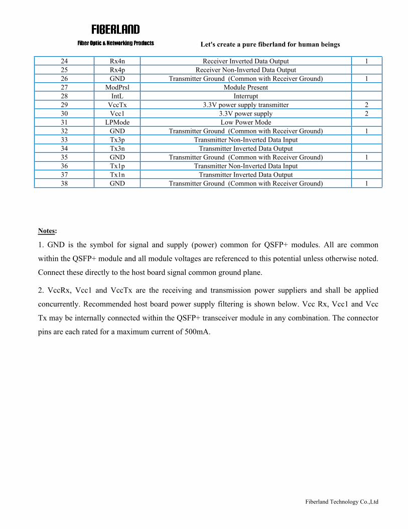
24 Rx4n Receiver Inverted Data Output 125 Rx4p Receiver Non-Inverted Data Output26 GND Transmitter Ground (Common with Receiver Ground) 127 ModPrsl Module Present28 IntL Interrupt29 VccTx 3.3V power supply transmitter 230 Vcc1 3.3V power supply 231 LPMode Low Power Mode32 GND Transmitter Ground (Common with Receiver Ground) 133 Tx3p Transmitter Non-Inverted Data Input34 Tx3n Transmitter Inverted Data Output35 GND Transmitter Ground (Common with Receiver Ground) 136 Tx1p Transmitter Non-Inverted Data Input37 Tx1n Transmitter Inverted Data Output38 GND Transmitter Ground (Common with Receiver Ground) 1
Notes:
1. GND is the symbol for signal and supply (power) common for QSFP+ modules. All are common
within the QSFP+ module and all module voltages are referenced to this potential unless otherwise noted.
Connect these directly to the host board signal common ground plane.
2. VccRx, Vcc1 and VccTx are the receiving and transmission power suppliers and shall be applied
concurrently. Recommended host board power supply filtering is shown below. Vcc Rx, Vcc1 and Vcc
Tx may be internally connected within the QSFP+ transceiver module in any combination. The connector
pins are each rated for a maximum current of 500mA.
Let's create a pure fiberland for human beings
Fiberland Technology Co.,Ltd
VI. Digital Diagnostic Functions
FLD-QSFP+LR4 supports the 2-wire serial communication protocol as defined in the QSFP+ MSA.
which allows real-time access to the following operating parameters:
Transceiver temperature
Laser bias current
Transmitted optical power
Received optical power
Transceiver supply voltage
It also provides a sophisticated system of alarm and warning flags, which may be used to alert end-users
when particular operating parameters are outside of a factory-set normal range.
The operating and diagnostics information is monitored and reported by a Digital Diagnostics Transceiver
Controller (DDTC) inside the transceiver, which is accessed through the 2-wire serial interface. When the
serial protocol is activated, the serial clock signal (SCL pin) is generated by the host. The positive edge
clocks data into the QSFP+ transceiver into those segments of its memory map that are not write-
protected. The negative edge clocks data from the QSFP+ transceiver. The serial data signal (SDA pin) is
bi-directional for serial data transfer. The host uses SDA in conjunction with SCL to mark the start and
end of serial protocol activation. The memories are organized as a series of 8-bit data words that can be
addressed individually or sequentially. The 2-wire serial interface provides sequential or random access to
the 8 bit parameters, addressed from 000h to the maximum address of the memory.
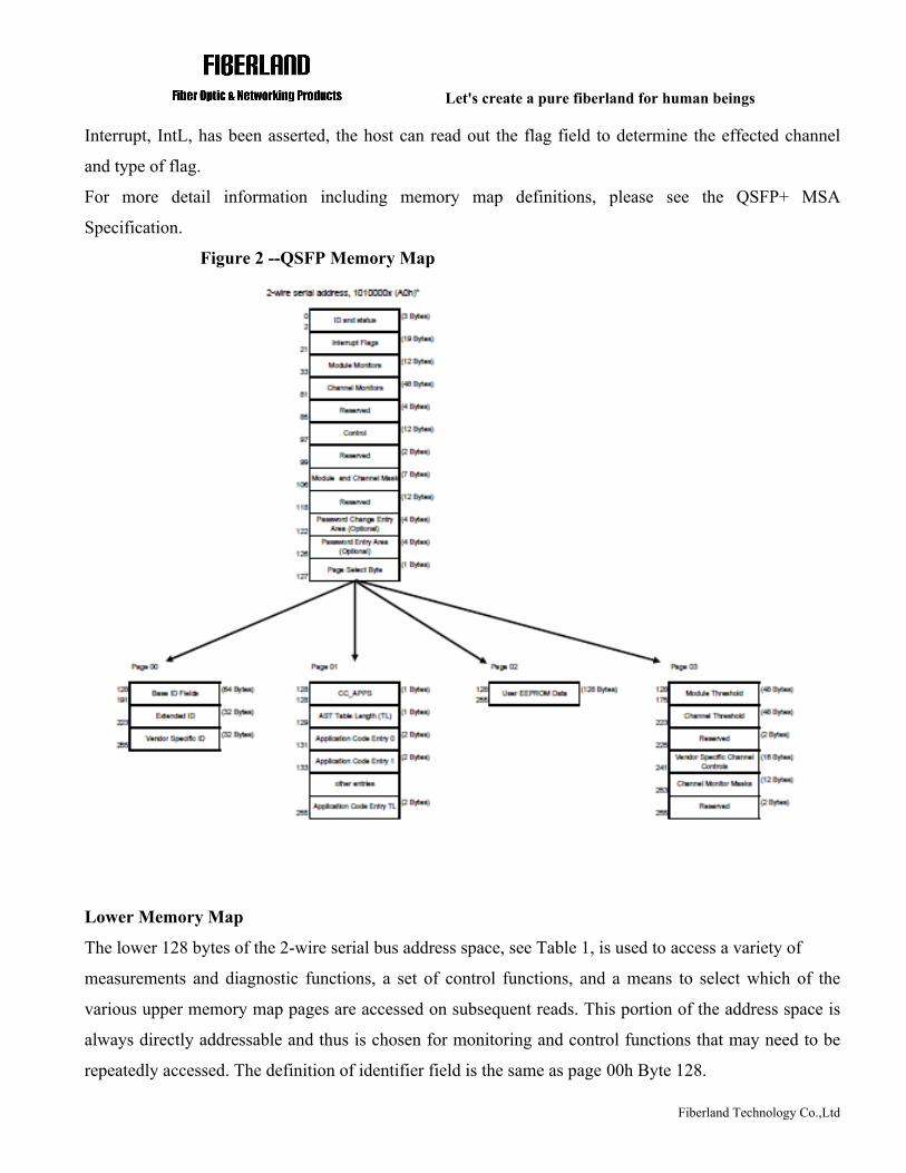
This clause defines the Memory Map for QSFP transceiver used for serial ID, digital monitoring and
certain control functions. The interface is mandatory for all QSFP devices. The memory map has been
changed in order to accommodate 4 optical channels and limit the required memory space. The structure
of the memory is shown in Figure 2 -QSFP+ Memory Map. The memory space is arranged into a lower,
single page, address space of 128 bytes and multiple upper address space pages. This structure permits
timely access to addresses in the lower page, e.g. Interrupt Flags and Monitors. Less time critical entries,
e.g. serial ID information and threshold settings, are available with the Page Select function. The structure
also provides address expansion by adding additional upper pages as needed. For example, in Figure 29
upper pages 01 and 02 are optional. Upper page 01 allows implementation of Application Select Table,
and upper page 02 provides user read/write space. The lower page and upper pages 00 and 03 are always
implemented. The interface address used is A0xh and is mainly used for time critical data like interrupt
handling in order to enable a “one-time-read” for all data related to an interrupt situation. After an
Let's create a pure fiberland for human beings
Fiberland Technology Co.,Ltd
Interrupt, IntL, has been asserted, the host can read out the flag field to determine the effected channel
and type of flag.
For more detail information including memory map definitions, please see the QSFP+ MSA
Specification.
Figure 2 --QSFP Memory Map
Lower Memory Map
The lower 128 bytes of the 2-wire serial bus address space, see Table 1, is used to access a variety of
measurements and diagnostic functions, a set of control functions, and a means to select which of the
various upper memory map pages are accessed on subsequent reads. This portion of the address space is
always directly addressable and thus is chosen for monitoring and control functions that may need to be
repeatedly accessed. The definition of identifier field is the same as page 00h Byte 128.
Let's create a pure fiberland for human beings
Fiberland Technology Co.,Ltd
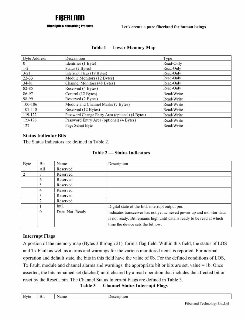
Table 1— Lower Memory Map
Byte Address Description Type0 Identifier (1 Byte) Read-Only1-2 Status (2 Bytes) Read-Only3-21 Interrupt Flags (19 Bytes) Read-Only22-33 Module Monitors (12 Bytes) Read-Only34-81 Channel Monitors (48 Bytes) Read-Only82-85 Reserved (4 Bytes) Read-Only86-97 Control (12 Bytes) Read/Write98-99 Reserved (2 Bytes) Read/Write100-106 Module and Channel Masks (7 Bytes) Read/Write107-118 Reserved (12 Bytes) Read/Write119-122 Password Change Entry Area (optional) (4 Bytes) Read/Write123-126 Password Entry Area (optional) (4 Bytes) Read/Write127 Page Select Byte Read/Write
Status Indicator BitsThe Status Indicators are defined in Table 2.
Table 2 — Status Indicators
Byte Bit Name Description1 All Reserved2 7 Reserved
6 Reserved5 Reserved4 Reserved3 Reserved2 Reserved1 IntL Digital state of the IntL interrupt output pin.0 Data_Not_Ready Indicates transceiver has not yet achieved power up and monitor data
is not ready. Bit remains high until data is ready to be read at which time the device sets the bit low.
Interrupt FlagsA portion of the memory map (Bytes 3 through 21), form a flag field. Within this field, the status of LOS and Tx Fault as well as alarms and warnings for the various monitored items is reported. For normal operation and default state, the bits in this field have the value of 0b. For the defined conditions of LOS, Tx Fault, module and channel alarms and warnings, the appropriate bit or bits are set, value = 1b. Once asserted, the bits remained set (latched) until cleared by a read operation that includes the affected bit or reset by the ResetL pin. The Channel Status Interrupt Flags are defined in Table 3.
Table 3 — Channel Status Interrupt Flags
Byte Bit Name Description
Let's create a pure fiberland for human beings
Fiberland Technology Co.,Ltd
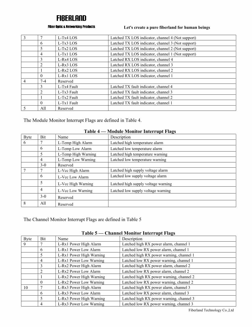
3 7 L-Tx4 LOS Latched TX LOS indicator, channel 4 (Not support)6 L-Tx3 LOS Latched TX LOS indicator, channel 3 (Not support)5 L-Tx2 LOS Latched TX LOS indicator, channel 2 (Not support)4 L-Tx1 LOS Latched TX LOS indicator, channel 1 (Not support)3 L-Rx4 LOS Latched RX LOS indicator, channel 42 L-Rx3 LOS Latched RX LOS indicator, channel 31 L-Rx2 LOS Latched RX LOS indicator, channel 20 L-Rx1 LOS Latched RX LOS indicator, channel 1
4 7-4 Reserved3 L-Tx4 Fault Latched TX fault indicator, channel 42 L-Tx3 Fault Latched TX fault indicator, channel 31 L-Tx2 Fault Latched TX fault indicator, channel 20 L-Tx1 Fault Latched TX fault indicator, channel 1
5 All Reserved
The Module Monitor Interrupt Flags are defined in Table 4.
Table 4 — Module Monitor Interrupt FlagsByte Bit Name Description6 7 L-Temp High Alarm Latched high temperature alarm
6 L-Temp Low Alarm Latched low temperature alarm5 L-Temp High Warning Latched high temperature warning4 L-Temp Low Warning Latched low temperature warning3-0 Reserved
7 7 L-Vcc High Alarm Latched high supply voltage alarm6 L-Vcc Low Alarm Latched low supply voltage alarm
5 L-Vcc High Warning Latched high supply voltage warning4 L-Vcc Low Warning Latched low supply voltage warning3-0 Reserved
8 All Reserved
The Channel Monitor Interrupt Flags are defined in Table 5
Table 5 — Channel Monitor Interrupt FlagsByte Bit Name Description9 7 L-Rx1 Power High Alarm Latched high RX power alarm, channel 1
6 L-Rx1 Power Low Alarm Latched low RX power alarm, channel 15 L-Rx1 Power High Warning Latched high RX power warning, channel 14 L-Rx1 Power Low Warning Latched low RX power warning, channel 13 L-Rx2 Power High Alarm Latched high RX power alarm, channel 22 L-Rx2 Power Low Alarm Latched low RX power alarm, channel 21 L-Rx2 Power High Warning Latched high RX power warning, channel 20 L-Rx2 Power Low Warning Latched low RX power warning, channel 2
10 7 L-Rx3 Power High Alarm Latched high RX power alarm, channel 36 L-Rx3 Power Low Alarm Latched low RX power alarm, channel 35 L-Rx3 Power High Warning Latched high RX power warning, channel 34 L-Rx3 Power Low Warning Latched low RX power warning, channel 3
Let's create a pure fiberland for human beings
Fiberland Technology Co.,Ltd
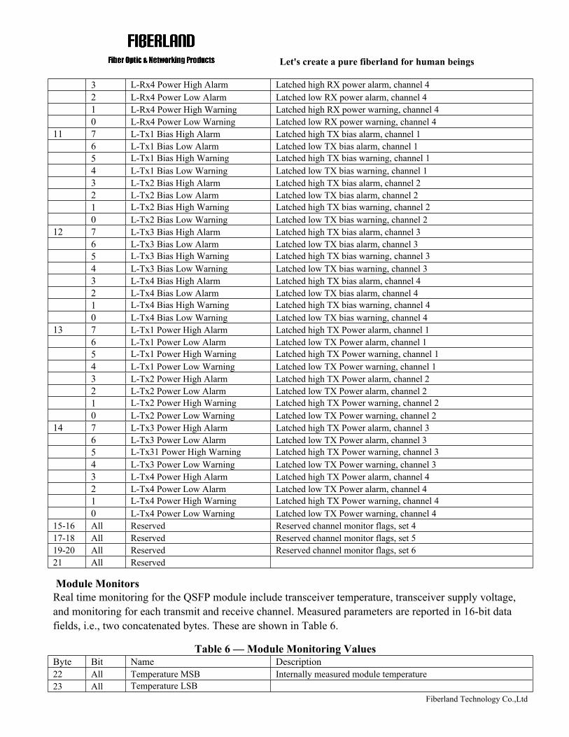
3 L-Rx4 Power High Alarm Latched high RX power alarm, channel 42 L-Rx4 Power Low Alarm Latched low RX power alarm, channel 41 L-Rx4 Power High Warning Latched high RX power warning, channel 40 L-Rx4 Power Low Warning Latched low RX power warning, channel 4
11 7 L-Tx1 Bias High Alarm Latched high TX bias alarm, channel 16 L-Tx1 Bias Low Alarm Latched low TX bias alarm, channel 15 L-Tx1 Bias High Warning Latched high TX bias warning, channel 14 L-Tx1 Bias Low Warning Latched low TX bias warning, channel 13 L-Tx2 Bias High Alarm Latched high TX bias alarm, channel 22 L-Tx2 Bias Low Alarm Latched low TX bias alarm, channel 21 L-Tx2 Bias High Warning Latched high TX bias warning, channel 20 L-Tx2 Bias Low Warning Latched low TX bias warning, channel 2
12 7 L-Tx3 Bias High Alarm Latched high TX bias alarm, channel 36 L-Tx3 Bias Low Alarm Latched low TX bias alarm, channel 35 L-Tx3 Bias High Warning Latched high TX bias warning, channel 34 L-Tx3 Bias Low Warning Latched low TX bias warning, channel 33 L-Tx4 Bias High Alarm Latched high TX bias alarm, channel 42 L-Tx4 Bias Low Alarm Latched low TX bias alarm, channel 41 L-Tx4 Bias High Warning Latched high TX bias warning, channel 40 L-Tx4 Bias Low Warning Latched low TX bias warning, channel 4
13 7 L-Tx1 Power High Alarm Latched high TX Power alarm, channel 16 L-Tx1 Power Low Alarm Latched low TX Power alarm, channel 15 L-Tx1 Power High Warning Latched high TX Power warning, channel 14 L-Tx1 Power Low Warning Latched low TX Power warning, channel 13 L-Tx2 Power High Alarm Latched high TX Power alarm, channel 22 L-Tx2 Power Low Alarm Latched low TX Power alarm, channel 21 L-Tx2 Power High Warning Latched high TX Power warning, channel 20 L-Tx2 Power Low Warning Latched low TX Power warning, channel 2
14 7 L-Tx3 Power High Alarm Latched high TX Power alarm, channel 36 L-Tx3 Power Low Alarm Latched low TX Power alarm, channel 35 L-Tx31 Power High Warning Latched high TX Power warning, channel 34 L-Tx3 Power Low Warning Latched low TX Power warning, channel 33 L-Tx4 Power High Alarm Latched high TX Power alarm, channel 42 L-Tx4 Power Low Alarm Latched low TX Power alarm, channel 41 L-Tx4 Power High Warning Latched high TX Power warning, channel 40 L-Tx4 Power Low Warning Latched low TX Power warning, channel 4
15-16 All Reserved Reserved channel monitor flags, set 417-18 All Reserved Reserved channel monitor flags, set 519-20 All Reserved Reserved channel monitor flags, set 621 All Reserved
Module MonitorsReal time monitoring for the QSFP module include transceiver temperature, transceiver supply voltage, and monitoring for each transmit and receive channel. Measured parameters are reported in 16-bit data fields, i.e., two concatenated bytes. These are shown in Table 6.
Table 6 — Module Monitoring ValuesByte Bit Name Description22 All Temperature MSB Internally measured module temperature23 All Temperature LSB
Let's create a pure fiberland for human beings
Fiberland Technology Co.,Ltd
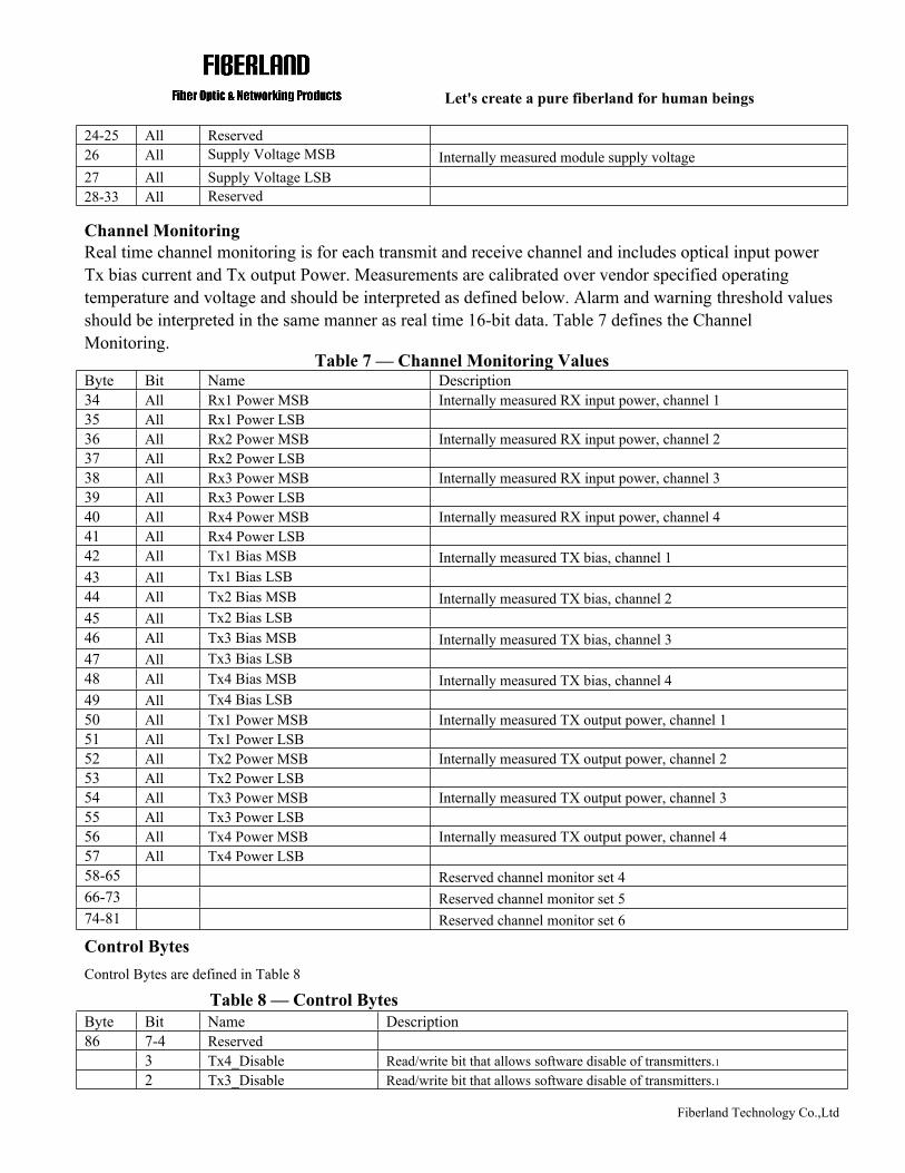
24-25 All Reserved26 All Supply Voltage MSB Internally measured module supply voltage27 All Supply Voltage LSB28-33 All Reserved
Channel MonitoringReal time channel monitoring is for each transmit and receive channel and includes optical input power Tx bias current and Tx output Power. Measurements are calibrated over vendor specified operating temperature and voltage and should be interpreted as defined below. Alarm and warning threshold values should be interpreted in the same manner as real time 16-bit data. Table 7 defines the Channel Monitoring.
Table 7 — Channel Monitoring ValuesByte Bit Name Description34 All Rx1 Power MSB Internally measured RX input power, channel 135 All Rx1 Power LSB36 All Rx2 Power MSB Internally measured RX input power, channel 237 All Rx2 Power LSB38 All Rx3 Power MSB Internally measured RX input power, channel 339 All Rx3 Power LSB40 All Rx4 Power MSB Internally measured RX input power, channel 441 All Rx4 Power LSB42 All Tx1 Bias MSB Internally measured TX bias, channel 143 All Tx1 Bias LSB44 All Tx2 Bias MSB Internally measured TX bias, channel 245 All Tx2 Bias LSB46 All Tx3 Bias MSB Internally measured TX bias, channel 347 All Tx3 Bias LSB48 All Tx4 Bias MSB Internally measured TX bias, channel 449 All Tx4 Bias LSB50 All Tx1 Power MSB Internally measured TX output power, channel 151 All Tx1 Power LSB52 All Tx2 Power MSB Internally measured TX output power, channel 253 All Tx2 Power LSB54 All Tx3 Power MSB Internally measured TX output power, channel 355 All Tx3 Power LSB56 All Tx4 Power MSB Internally measured TX output power, channel 457 All Tx4 Power LSB58-65 Reserved channel monitor set 466-73 Reserved channel monitor set 574-81 Reserved channel monitor set 6
Control BytesControl Bytes are defined in Table 8
Table 8 — Control BytesByte Bit Name Description86 7-4 Reserved
3 Tx4_Disable Read/write bit that allows software disable of transmitters.12 Tx3_Disable Read/write bit that allows software disable of transmitters.1
Let's create a pure fiberland for human beings
Fiberland Technology Co.,Ltd
1 Tx2_Disable Read/write bit that allows software disable of transmitters.10 Tx1_Disable Read/write bit that allows software disable of transmitters.1
87 7 Rx4_Rate_Select Software Rate Select, Rx channel 4 msb 6 Rx4_Rate_Select Software Rate Select, Rx channel 4 lsb 5 Rx3_Rate_Select Software Rate Select, Rx channel 3 msb 4 Rx3_Rate_Select Software Rate Select, Rx channel 3 lsb 3 Rx2_Rate_Select Software Rate Select, Rx channel 2 msb 2 Rx2_Rate_Select Software Rate Select, Rx channel 2 lsb 1 Rx1_Rate_Select Software Rate Select, Rx channel 1 msb 0 Rx1_Rate_Select Software Rate Select, Rx channel 1 lsb
88 7 Tx4_Rate_Select Software Rate Select, Tx channel 4 msb (Not support)6 Tx4_Rate_Select Software Rate Select, Tx channel 4 lsb (Not support)5 Tx3_Rate_Select Software Rate Select, Tx channel 3 msb (Not support)4 Tx3_Rate_Select Software Rate Select, Tx channel 3 lsb (Not support)3 Tx2_Rate_Select Software Rate Select, Tx channel 2 msb (Not support)2 Tx2_Rate_Select Software Rate Select, Tx channel 2 lsb (Not support)1 Tx1_Rate_Select Software Rate Select, Tx channel 1 msb (Not support)0 Tx1_Rate_Select Software Rate Select, Tx channel 1 lsb (Not support)
89 All Rx4_Application_Select Software Application Select per SFF-8079, Rx Channel 4 90 All Rx3_Application_Select Software Application Select per SFF-8079, Rx Channel 3 91 All Rx2_Application_Select Software Application Select per SFF-8079, Rx Channel 2 92 All Rx1_Application_Select Software Application Select per SFF-8079, Rx Channel 1 93 2-7 Reserved
1 Power_set Power set to low power mode. Default 0.0 Power_over-ride Override of LPMode signal setting the power mode with software.
94 All Tx4_Application_Select Software Application Select per SFF-8079, Tx Channel 4 (Not support)95 All Tx3_Application_Select Software Application Select per SFF-8079, Tx Channel 3 (Not support)96 All Tx2_Application_Select Software Application Select per SFF-8079, Tx Channel 2 (Not support)97 All Tx1_Application_Select Software Application Select per SFF-8079, Tx Channel 1 (Not support)98-99 All Reserved1. Writing “1” disables the laser of the channel.
LPModeThe LPMode pin shall be pulled up to Vcc in the QSFP module. This function is affected by the LPMode pin and the
combination of the Power_over-ride and Power_set software control bits (Address A0h, byte 93 bits
0,1).
The module has two modes a low power mode and a high power mode. When the module is in a low power mode it has a
maximum power consumption of 1.5W. This protects hosts that are not capable of cooling higher power modules, should
such modules be accidentally inserted. A truth table for the relevant configurations of the LPMode and the Power_over-ride
and Power_set are shown in Table 9.
At Power up, the Power_over-ride and Power_set bits shall be set to 0.
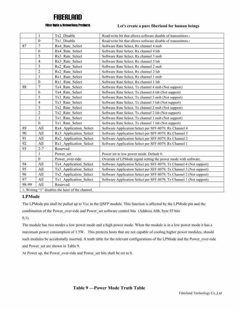
Table 9 —Power Mode Truth Table
Let's create a pure fiberland for human beings
Fiberland Technology Co.,Ltd
LPMode Power_Over-ride Bit Power_set Bit Module Power Al owed1 0 X Low Power0 0 X High PowerX 1 1 Low PowerX 1 0 High Power
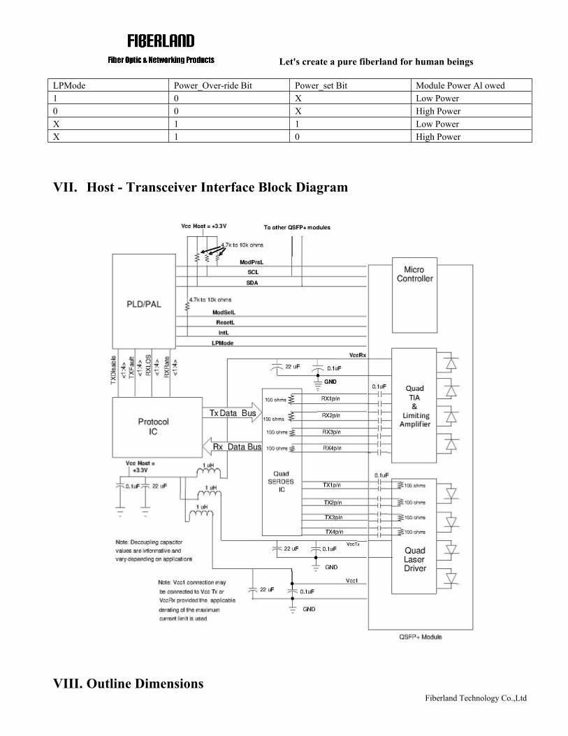
VII. Host - Transceiver Interface Block Diagram
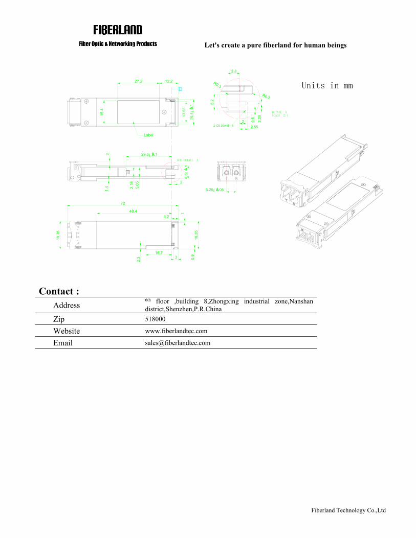
VIII. Outline Dimensions
Let's create a pure fiberland for human beings
Fiberland Technology Co.,Ltd
Units in mm
2.55
16.4¡À0.1
Label
0.9
R0.3
15.4
27.2 12.2
13.68
R0.2
2-C0.35X45¡ ã
3.8
5.2
12.25
0.6
2
1.4
3
5.85
2.15
29.6¡ À0.1
8.5¡À0.1
2
18.35
72
2.3
48.44.2
16.73
1
18.35
D
6.25¡ À0.05
SEE DETAIL A
DETAIL ASCALE 2:1
Contact :Address
6th floor ,building 8,Zhongxing industrial zone,Nanshan district,Shenzhen,P.R.China
Zip 518000
Website www.fiberlandtec.com
Email [email protected]