Embed Size (px)
DESCRIPTION
טכניון – מכון טכנולוגי לישראל הפקולטה להנדסת חשמל. PowerPC based reliable computer. Part A presentation. Students: Guy Derry Gil Wiechman Instructor: Isaschar Walter Winter 2003. Problem: - PowerPoint PPT Presentation
Citation preview

Students: Guy Derry
Gil Wiechman
Instructor: Isaschar Walter
Winter 2003
Students: Guy Derry
Gil Wiechman
Instructor: Isaschar Walter
Winter 2003
טכניון – מכון טכנולוגי לישראלהפקולטה להנדסת חשמל
PowerPC based reliable computer
PowerPC based reliable computer
Part A presentationPart A presentation
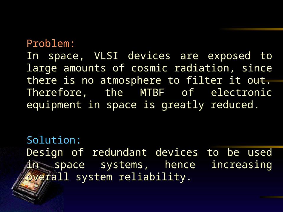
Problem:In space, VLSI devices are exposed to large amounts of cosmic radiation, since there is no atmosphere to filter it out.Therefore, the MTBF of electronic equipment in space is greatly reduced.
Problem:In space, VLSI devices are exposed to large amounts of cosmic radiation, since there is no atmosphere to filter it out.Therefore, the MTBF of electronic equipment in space is greatly reduced.
Solution:Design of redundant devices to be used in space systems, hence increasing overall system reliability.
Solution:Design of redundant devices to be used in space systems, hence increasing overall system reliability.
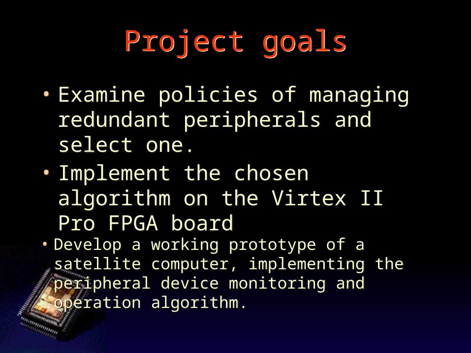
Project goalsProject goals
• Develop a working prototype of a satellite computer, implementing the peripheral device monitoring and operation algorithm.
• Develop a working prototype of a satellite computer, implementing the peripheral device monitoring and operation algorithm.
• Examine policies of managing redundant peripherals and select one.
• Examine policies of managing redundant peripherals and select one.
• Implement the chosen algorithm on the Virtex II Pro FPGA board
• Implement the chosen algorithm on the Virtex II Pro FPGA board
Implementation toolsImplementation tools
The project is implemented using the following tools:
Project AssumptionsProject Assumptions
In this project, we assume correct operation of the software, on a correctly operating single processor.In this project, we assume correct operation of the software, on a correctly operating single processor.
The issue of multiple processors handling is examined under a different project, running concurrently to ours.The issue of multiple processors handling is examined under a different project, running concurrently to ours.
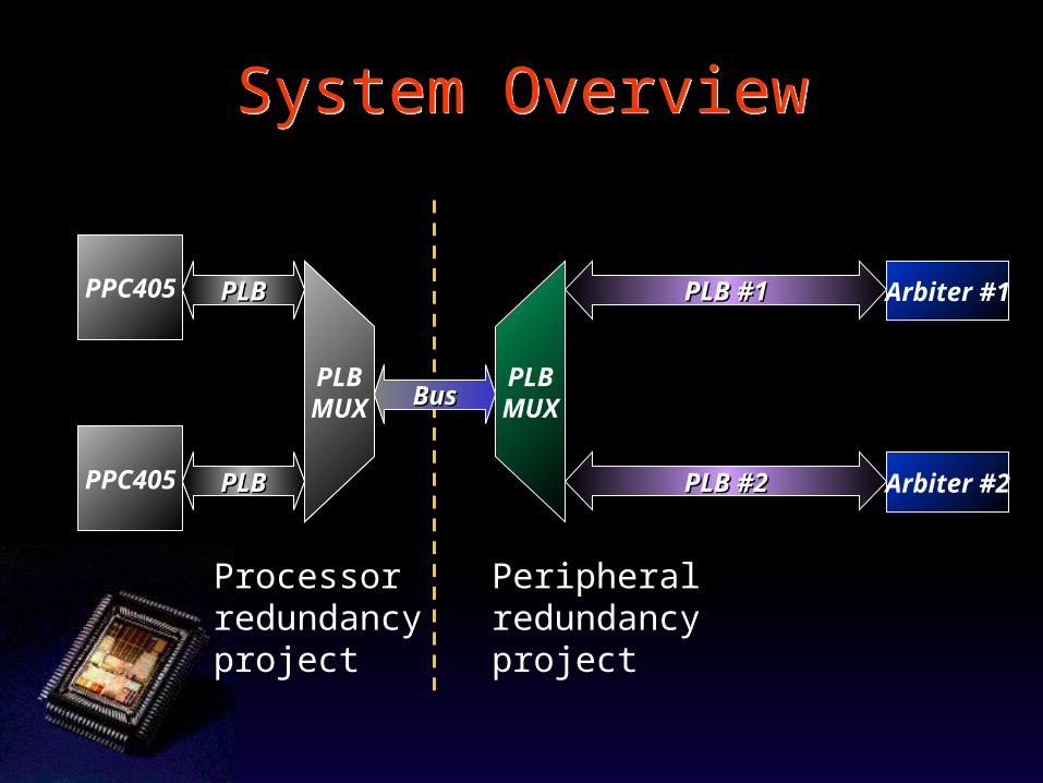
PPC405 PLBPLB
PLBMUX
PPC405 PLBPLB
BusBus
System OverviewSystem Overview
Arbiter #1
PLBMUX
PLB #1PLB #1
PLB #2PLB #2 Arbiter #2
Peripheralredundancyproject
Processorredundancyproject
PPC405 PLBPLB
PLBMUX
PPC405 PLBPLB
BusBus
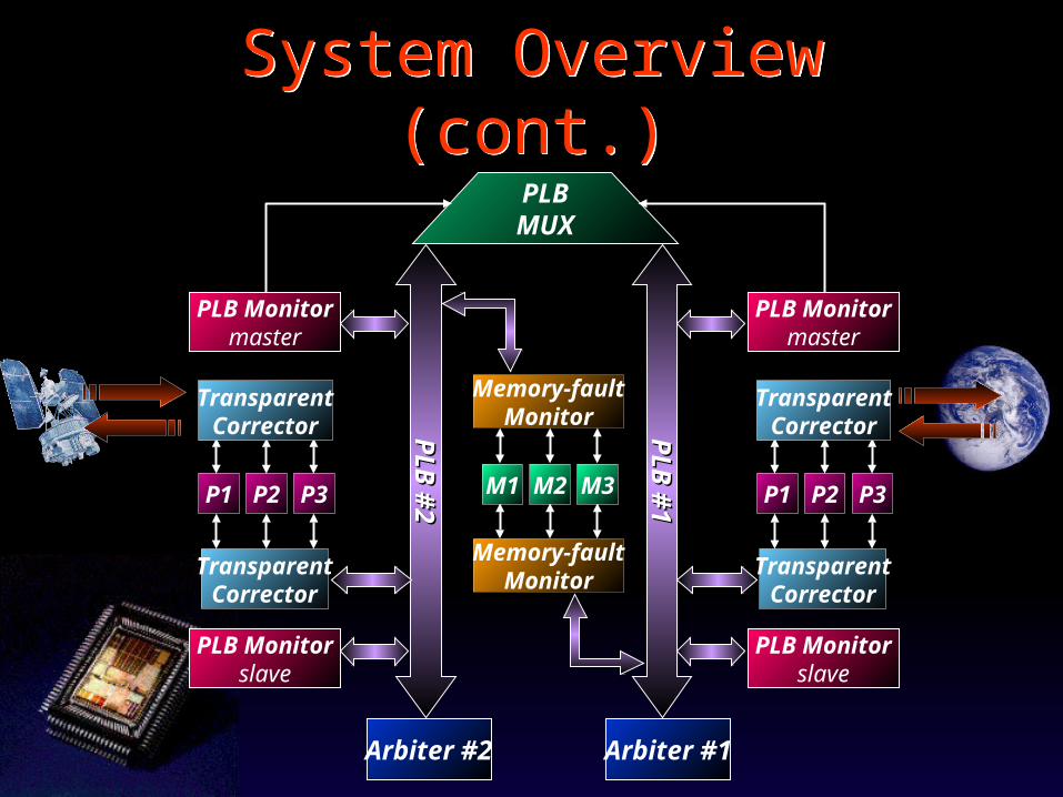
System Overview (cont.)System Overview (cont.)PLBMUX
PL
B #1
PL
B #1
PL
B #2
PL
B #2
Arbiter #1Arbiter #2
Memory-faultMonitor
Memory-faultMonitor
M1 M2 M3 P1 P2 P3P1 P2 P3
TransparentCorrector
TransparentCorrector
TransparentCorrector
TransparentCorrector
PLB Monitormaster
PLB Monitorslave
PLB Monitormaster
PLB Monitorslave
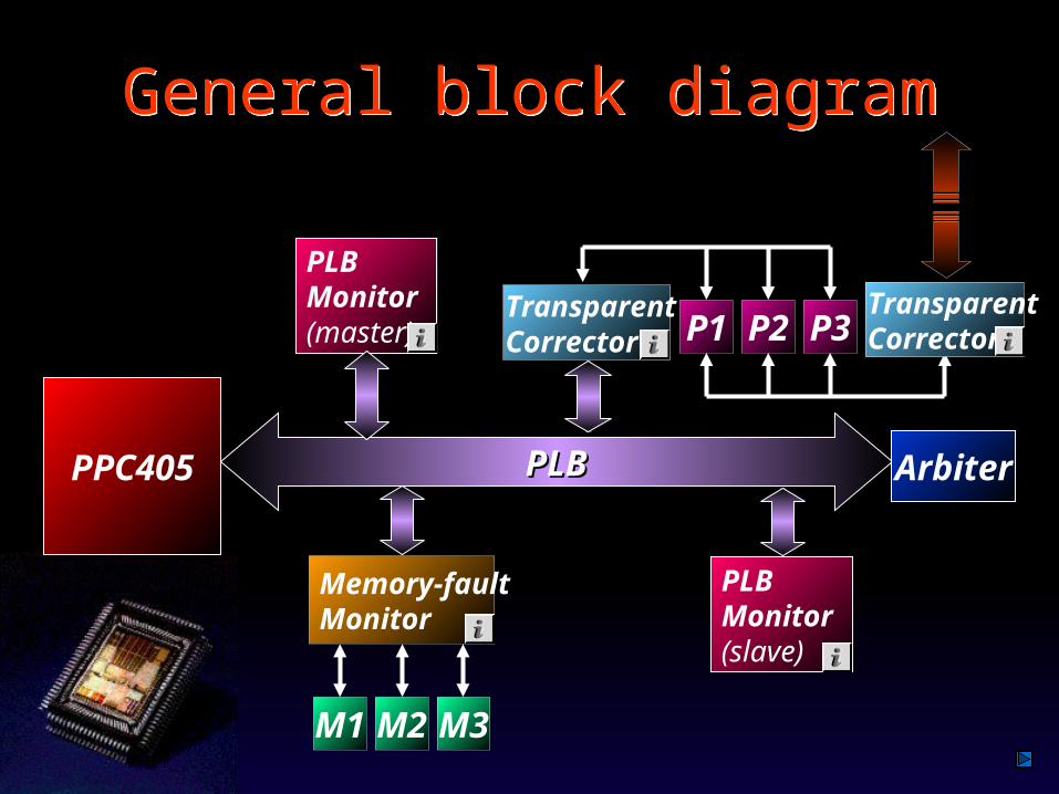
PPC405
General block diagramGeneral block diagram
P1 P2 P3
PLBPLB Arbiter
M1 M2 M3
Memory-faultMonitor
PLBMonitor(master)
PLBMonitor(slave)
TransparentCorrector
TransparentCorrector

PLB Monitor - MasterPLB Monitor - Master
Read_Odd
Countdown
Reset_Bus
Read_Even
State description:Countdown: count N clock cycles
Read_Even / Read_Odd :Read from slave unit address #1/2.If expected value is not received, try again until success or three consequent failures.
Reset_Bus:Reset the bus, and read it.If bus is not reset to zero, try again until success or three consequent failures.
ALL TESTS:3 consequent failures Interrupt to CPU.ALL TESTS:3 consequent failures Interrupt to CPU.

PLB Monitor – Master:implementation (1/3)
PLB Monitor – Master:implementation (1/3)
Read Even / Odd:
Request#1
Ack.#1
Request#2
Ack.#2
Request#3
Ack.#3
Nextcheckup
Faultinterrupt
Prev.checkup
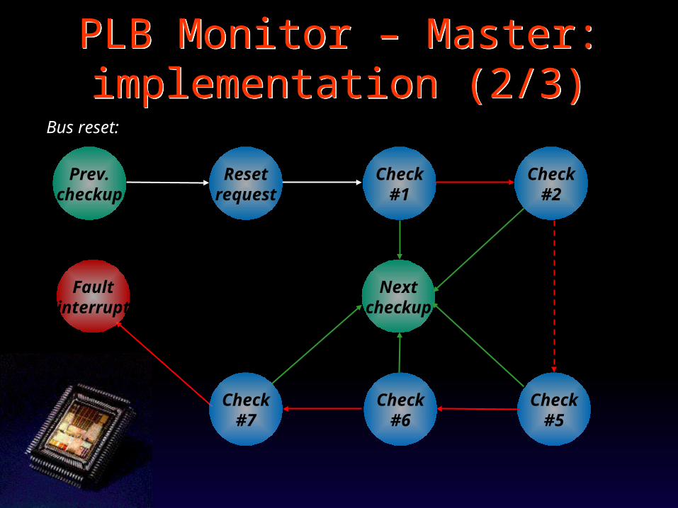
PLB Monitor – Master:implementation (2/3)
PLB Monitor – Master:implementation (2/3)
Bus reset:
Resetrequest
Check#7
Check#1
Check#6
Check#2
Check#5
Nextcheckup
Faultinterrupt
Prev.checkup
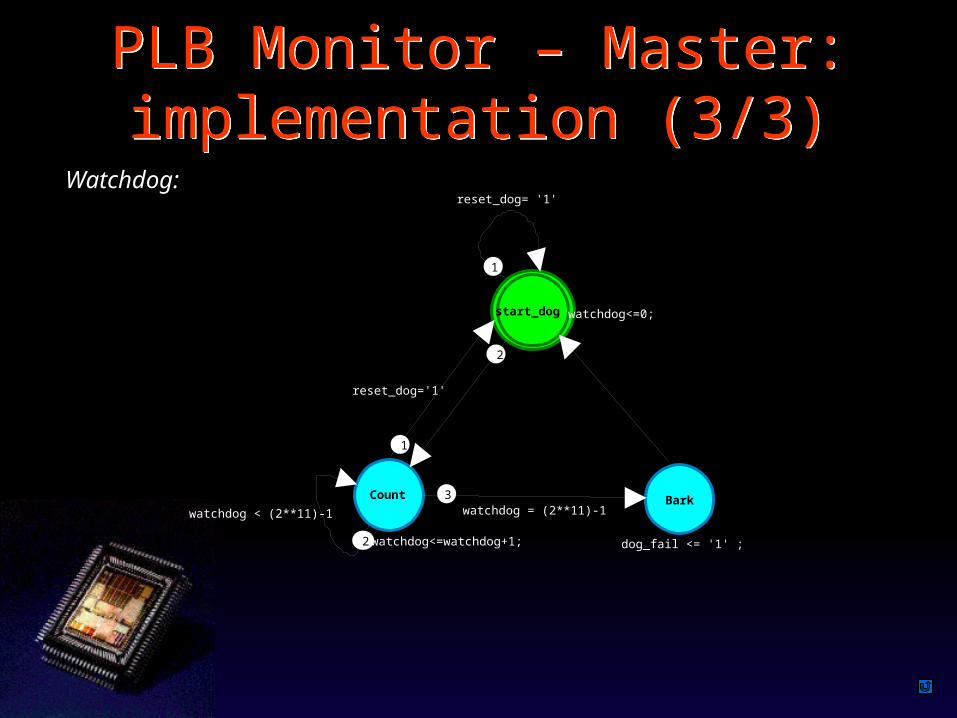
PLB Monitor – Master:implementation (3/3)
PLB Monitor – Master:implementation (3/3)
Watchdog:
start_dog
watchdog = (2**11)-1
reset_dog= '1'
2
1
watchdog<=0;
Count
2
3
reset_dog='1'
1
watchdog < (2**11)-1
watchdog<=watchdog+1;
Bark
dog_fail <= '1' ;
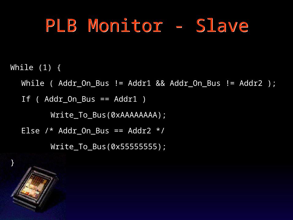
PLB Monitor - SlavePLB Monitor - Slave
While (1) {
While ( Addr_On_Bus != Addr1 && Addr_On_Bus != Addr2 );
If ( Addr_On_Bus == Addr1 )
Write_To_Bus(0xAAAAAAAA);
Else /* Addr_On_Bus == Addr2 */
Write_To_Bus(0x55555555);
}
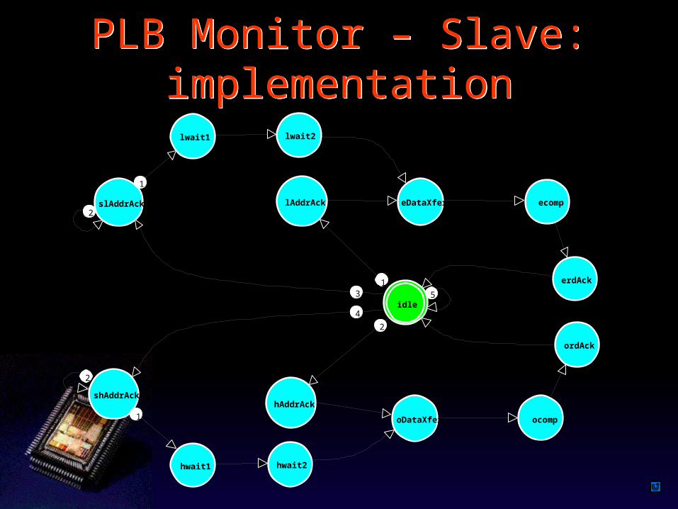
PLB Monitor – Slave:implementation
PLB Monitor – Slave:implementation
lwait1
slAddrAck
1
2
lwait2
idle
lAddrAck eDataXfer
13
4
5
erdAck
ecomp
hwait1
shAddrAck
1
2
hwait2
hAddrAck
oDataXfer
2
ordAck
ocomp
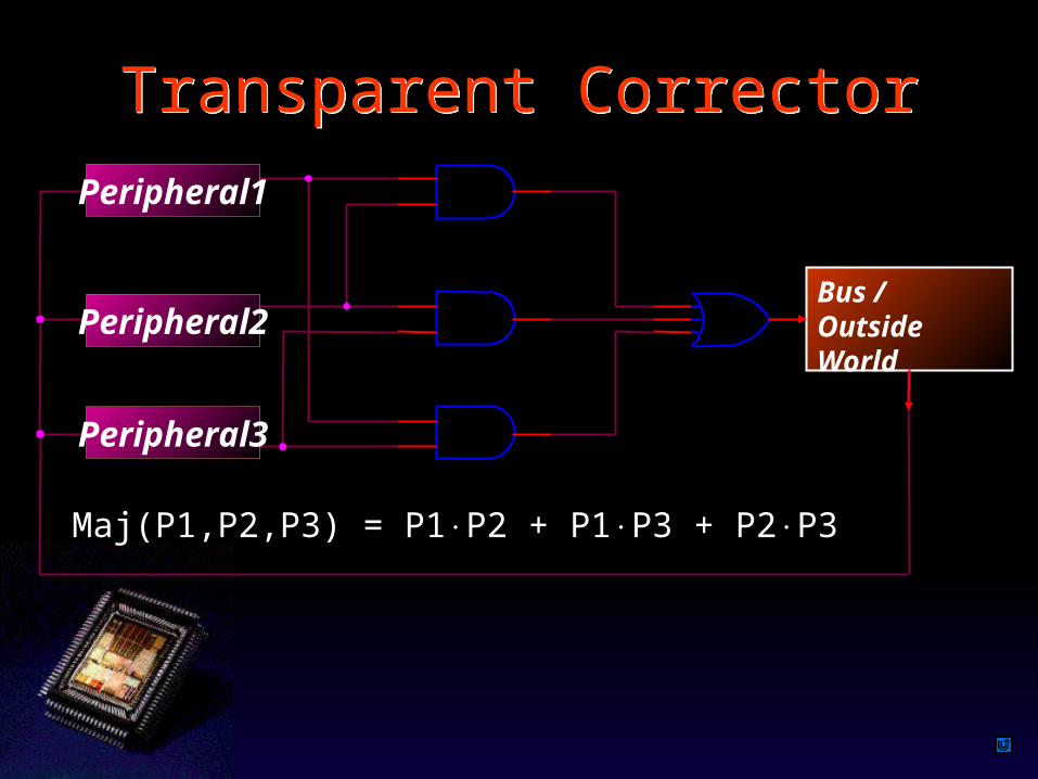
Transparent CorrectorTransparent Corrector
Maj(P1,P2,P3) = P1P2 + P1P3 + P2P3
Bus / Outside World
Peripheral1
Peripheral2
Peripheral3
Memory-Fault MonitorMemory-Fault MonitorDescription:
Sits between the PLB bus and memory controllers. On a write, performs a write to four different addresses, the writes are
checked (reads are performed) and thus each of the four memory blocks is graded.On a read performs a read from all four memory addresses and a bit wise majority vote on the top ranked three. All wrong memory addresses are corrected.When Idle, performs auto majority votes and correction on the most recently used addresses.
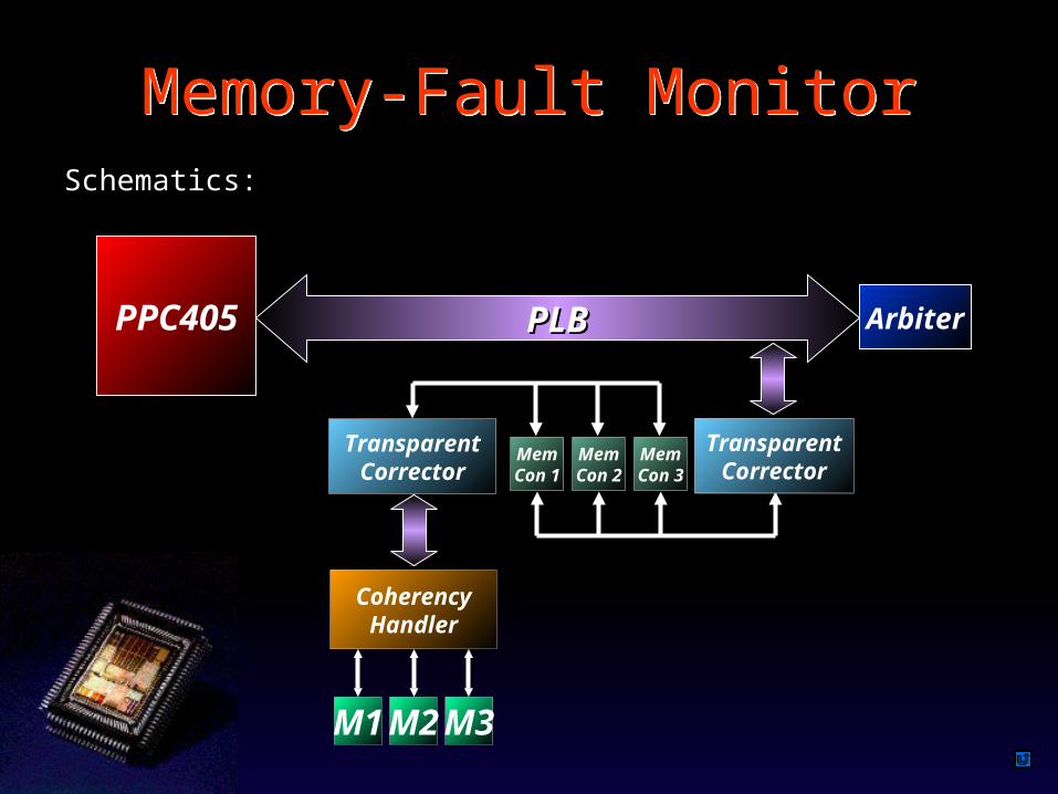
Memory-Fault MonitorMemory-Fault MonitorSchematics:
PPC405 PLBPLB Arbiter
M1 M2 M3
CoherencyHandler
MemCon 1
MemCon 2
MemCon 3
TransparentCorrector
TransparentCorrector
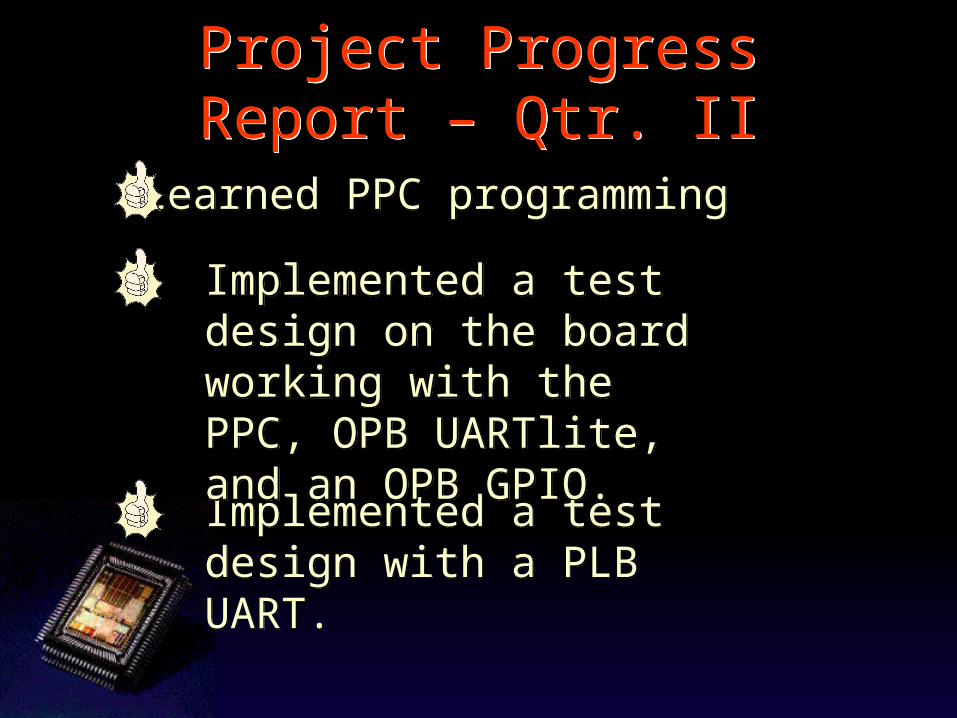
Project Progress Report – Qtr. IIProject Progress Report – Qtr. II
Learned PPC programmingLearned PPC programming
Implemented a test design with a PLB UART.Implemented a test design with a PLB UART.
Implemented a test design on the board working with the PPC, OPB UARTlite, and an OPB GPIO.
Implemented a test design on the board working with the PPC, OPB UARTlite, and an OPB GPIO.
Project Schedule – Qtr. II (cont.)
Project Schedule – Qtr. II (cont.)
Implemented transparent correctors. Implemented transparent correctors.
Developed an initial approach in memory coherency handling systemDeveloped an initial approach in memory coherency handling system
Implemented Master & Slave PLBmonitors.Implemented Master & Slave PLBmonitors.
Project schedule - First Semester Summary
Project schedule - First Semester Summary
• Synthesized a system on the FPGA including use of redundant peripherals and non redundant memory.
• Synthesized a system on the FPGA including use of redundant peripherals and non redundant memory.
• Multiple peripheral unit operation ability• Multiple peripheral unit operation ability
• Basically all the theoretical study is completed, and the bumpy start was overcome.
• Basically all the theoretical study is completed, and the bumpy start was overcome.
Project schedule - Second Semester
Project schedule - Second Semester
• Incorporate PLB monitoring implementations into design. (~2 weeks)
• Incorporate PLB monitoring implementations into design. (~2 weeks)
• Study interaction protocol between memory fault monitor and memory controllers.
(~1 week)
• Study interaction protocol between memory fault monitor and memory controllers.
(~1 week)
• Study memory management strategies and select one. (~1 week)
• Study memory management strategies and select one. (~1 week)
• Implement memory fault monitor. (~2 weeks)
• Implement memory fault monitor. (~2 weeks)
• Connect memory monitor to memory controllers and test on simulation tool.
(~1 week)
• Connect memory monitor to memory controllers and test on simulation tool.
(~1 week)
• Build a test bench for memory monitor.(~1 week)
• Build a test bench for memory monitor.(~1 week)
Project schedule - Second Semester
Project schedule - Second Semester (cont.
)(cont.
)
• Incorporate memory unit into the design and test it. (~2 weeks)
• Incorporate memory unit into the design and test it. (~2 weeks)
• Build the PLB-MUX.(~1 week)
• Build the PLB-MUX.(~1 week)
Project schedule - Second Semester
Project schedule - Second Semester (cont.
)(cont.
)
• Overall debugging.(~2
weeks)
• Overall debugging.(~2
weeks)
• Final goal: fully operative system incl. a simulation of an identification and correct operation in case of a faulty device.
• Final goal: fully operative system incl. a simulation of an identification and correct operation in case of a faulty device.
Project schedule - Second Semester
Project schedule - Second Semester (cont.
)(cont.
)