Embed Size (px)
Citation preview

PolyMUMPs Design
Handbook
a MUMPs® process
David Koester, Allen Cowen, Ramaswamy Mahadevan, Mark Stonefield, and Busbee Hardy MEMSCAP
Revision 10.0

Copyright © 2003 by MEMSCAP. All rights reserved.
Permission to use and copy for internal, noncommercial purposes is hereby granted. Any distribution of this manual or associated layouts or any part thereof is strictly prohibited without prior written consent of MEMSCAP Inc.
GDSII is a trademark of Calma, Valid, Cadence.
L-Edit and Tanner Database are trademarks of Tanner Research Inc.
Table of Contents Chapter 1
Three-Layer Polysilicon Surface Micromachining Process................................................................ 1 1.1 Introduction........................................................................................................................ 1 1.2 Process Overview................................................................................................................ 2
Chapter 2
PolyMUMPs Design Guidelines and Rules.................................................................................... 11 2.1 Introduction...................................................................................................................... 11 2.2 Design Rules..................................................................................................................... 12 2.3 Beyond the Design Rules..................................................................................................... 31 2.4 Film Parameters ................................................................................................................ 35 2.5 EZ-PolyMUMPs Design Rules................................................................................................ 38 2.6 Layout Requirements ......................................................................................................... 38 2.7 Layout Submission............................................................................................................. 39 2.8 Custom Dicing, Releasing and Critical Point Drying ................................................................. 39


3 - L A Y E R P O L Y S I L I C O N S U R F A C E M I C R O M A C H I N I N G P R O C E S S
1 PolyMUMPs Design Handbook, Rev. 10.0
Chapter 1 Three-Layer Polysilicon Surface Micromachining Process
1.1 Introduction The Multi-User MEMS Processes, or MUMPs®, is a commercial program that provides cost-effective, proof-of-concept MEMS fabrication to industry, universities, and government worldwide. MEMSCAP offers three standard processes as part of the MUMPs® program: PolyMUMPs, a three-layer polysilicon surface micromachining process: MetalMUMPs, an electroplated nickel process; and SOIMUMPs, a silicon-on-insulator micromachining process.
The following is a general process description and user guide for PolyMUMPs, which is designed for general-purpose micromachining of MEMS. Chapter 1 of this document explains the process step-by-step, while Chapter 2 outlines the design rules for the process.
Though this document is geared toward designers who do not have a strong background in microfabrication, it contains information that is useful to all PolyMUMPs users. Regardless of the level of the designer, we strongly recommend all users of PolyMUMPs review this document prior to submitting a design.

C H A P T E R 1
2 PolyMUMPs Design Handbook, Rev. 10.0
FIGURE 1.1. Cross sectional view showing all 7 layers of the PolyMUMPs process (not to scale).
Poly0 Poly1 Poly2 Metal
Nitride 1st Oxide 2nd Oxide
Figure 1.1 is a cross section of the three-layer polysilicon surface micromachining PolyMUMPs process. This process has the general features of a standard surface micromachining process: (1) polysilicon is used as the structural material, (2) deposited oxide (PSG) is used as the sacrificial layer, and silicon nitride is used as electrical isolation between the polysilicon and the substrate. The process is different from most customized surface micromachining processes in that it is designed to be as general as possible, and to be capable of supporting many different designs on a single silicon wafer. Since the process was not optimized with the purpose of fabricating any one specific device, the thicknesses of the structural and sacrificial layers were chosen to suit most users, and the layout design rules were chosen conservatively to guarantee the highest yield possible.
1.2 Process Overview The PolyMUMPs process is a three-layer polysilicon surface micromachining process derived from work performed at the Berkeley Sensors and Actuators Center (BSAC) at the University of California in the late 80’s and early 90’s. Several modifications and enhancements have been made to increase the flexibility and versatility of the process for the multi-user environment. The process flow described below is designed to introduce inexperienced users to polysilicon micromachining. The text is supplemented by detailed drawings that show the process flow in the context of building a typical micromotor.
The process begins with 100 mm n-type (100) silicon wafers of 1-2 Ω-cm resistivity. The surface of the wafers are first heavily doped with phosphorus in a standard diffusion furnace using POCl 3 as the dopant source. This helps to reduce or prevent charge feedthrough to the substrate from electrostatic devices on the surface. Next, a 600 nm low-stress LPCVD (low pressure chemical vapor deposition) silicon nitride layer is deposited on the wafers as an electrical isolation layer. This is followed directly by the deposition of a 500 nm LPCVD polysilicon film–Poly 0. Poly 0 is then patterned by photolithography, a process that includes the coating of the wafers with photoresist (Figure 1.2), exposure of the photoresist with the appropriate mask and developing the exposed photoresist to

3 - L A Y E R P O L Y S I L I C O N S U R F A C E M I C R O M A C H I N I N G P R O C E S S
3 PolyMUMPs Design Handbook, Rev. 10.0
create the desired etch mask for subsequent pattern transfer into the underlying layer (Figure 1.3). After patterning the photoresist, the Poly 0 layer is then etched in an RIE (Reactive Ion Etch) system (Figure 1.4). A 2.0 µm phosphosilicate glass (PSG) sacrificial layer is then deposited by LPCVD (Figure 1.5) and annealed @1050°C for 1 hour in argon. This layer of PSG, known as First Oxide, is removed at the end of the process to free the first mechanical layer of polysilicon. The sacrificial layer is lithographically patterned with the DIMPLES mask and the dimples are transferred into the sacrificial PSG layer by RIE, as shown in Figure 1.6. The nominal depth of the dimples is 750 nm. The wafers are then patterned with the third mask layer, ANCHOR1, and reactive ion etched (Figure 1.7). This step provides anchor holes that will be filled by the Poly 1 layer.
After etching ANCHOR1, the first structural layer of polysilicon (Poly 1) is deposited at a thickness of 2.0 µm. A thin (200 nm) layer of PSG is deposited over the polysilicon and the wafer is annealed at 1050°C for 1 hour (Figure 1.8). The anneal dopes the polysilicon with phosphorus from the PSG layers both above and below it. The anneal also serves to significantly reduce the net stress in the Poly 1 layer. The polysilicon (and its PSG masking layer) is lithographically patterned using a mask designed to form the first structural layer POLY1. The PSG layer is etched to produce a hard mask for the subsequent polysilicon etch. The hard mask is more resistant to the polysilicon etch chemistry than the photoresist and ensures better transfer of the pattern into the polysilicon. After etching the polysilicon (Figure 1.9), the photoresist is stripped and the remaining oxide hard mask is removed by RIE.
After Poly 1 is etched, a second PSG layer (Second Oxide) is deposited and annealed(Figure 1.10). The Second Oxide is patterned using two different etch masks with different objectives. The POLY1_POLY2_VIA level provides for etch holes in the Second Oxide down to the Poly 1 layer. This provide a mechanical and electrical connection between the Poly 1 and Poly 2 layers. The POLY1_POLY2_VIA layer is lithographically patterned and etched by RIE (Figure 1.11). The ANCHOR2 level is provided to etch both the First and Second Oxide layers in one step, thereby eliminating any misalignment between separately etched holes. More importantly, the ANCHOR2 etch eliminates the need to make a cut in First Oxide unrelated to anchoring a Poly 1 structure, which needlessly exposes the substrate to subsequent processing that can damage either Poly 0 or Nitride (see Section 2.3.3). The ANCHOR2 layer is lithographically patterned and etched by RIE in the same way as POLY1_POLY2_VIA.
Figure 1.12 shows the wafer cross section after both POLY1_POLY2_VIA and ANCHOR2 levels have been completed. The second structural layer, Poly 2, is then deposited (1.5 µm thick) followed by the deposition of 200 nm PSG. As with Poly 1, the thin PSG layer acts as both an etch mask and dopant source for Poly 2 (Figure 1.13). The wafer is annealed for one hour at 1050 C to dope the polysilicon and reduce the residual film stress. The Poly 2 layer is lithographically patterned with the seventh mask (POLY2) and the PSG and polysilicon layers are etched by RIE using the same processing conditions as for Poly 1. The photoresist then is stripped and the masking oxide is removed (Figure 1.14).
The final deposited layer in the PolyMUMPs process is a 0.5 µm metal layer that provides for probing, bonding, electrical routing and highly reflective mirror surfaces. The wafer is patterned lithographically with the eighth mask (METAL) and the metal is deposited and patterned using lift-off. The final, unreleased structure is shown in Figure 1.15. The wafers are diced, sorted and shipped to the PolyMUMPs user for sacrificial release and test. Figure 1.16 shows the device after sacrificial oxide release. The release is performed by immersing the chip in a bath of 49% HF (room temperature) for 1.5-2 minutes. This is followed by several minutes in DI water and then alcohol to reduce stiction followed by at least 10 minutes in an oven at 110° C.
Generally the participants receive their dice and perform the sacrificial oxide release in their own facility. For those participants who request it, release of their dice at MEMSCAP’s facility can be arranged for an additional fee.

C H A P T E R 1
4 PolyMUMPs Design Handbook, Rev. 10.0
The following provides a graphical representation of the process steps.
FIGURE 1.2. The surface of the starting n-type (100) wafers are heavily doped with phosphorus in a standard diffusion furnace using POCl 3 as the dopant source. A 600 nm blanket layer of low stress silicon nitride (Nitride) is deposited followed by a blanket layer of 500 nm polysilicon (Poly 0). The wafers are then coated with UV-sensitive photoresist.
FIGURE 1.3. The photoresist is lithographically patterned by exposing it to UV light through the first level mask (POLY0) and then developing it. The photoresist in exposed areas is removed leaving behind a patterned photoresist mask for etching.

3 - L A Y E R P O L Y S I L I C O N S U R F A C E M I C R O M A C H I N I N G P R O C E S S
5 PolyMUMPs Design Handbook, Rev. 10.0
FIGURE 1.4. Reactive ion etching (RIE) is used to remove the unwanted polysilicon. After the etch, the photoresist is chemically stripped in a solvent bath. This method of patterning the wafers with photoresist, etching and stripping the remaining photoresist is used repeatedly in the PolyMUMPs process.
FIGURE 1.5. A 2.0 µm layer of PSG is deposited on the wafers by low pressure chemical vapor deposition (LPCVD). This is the first sacrificial layer.
FIGURE 1.6. The wafers are coated with photoresist and the second level (DIMPLE) is lithographically patterned. The dimples, 750 nm deep, are reactive ion etched into the first oxide layer. After the etch, the photoresist is stripped.

C H A P T E R 1
6 PolyMUMPs Design Handbook, Rev. 10.0
FIGURE 1.7. The wafers are re-coated with photoresist and the third level (ANCHOR1) is lithographically patterned. The unwanted oxide is removed in an RIE etch and the photoresist is stripped.
FIGURE 1.8. A blanket 2.0 µm layer of un-doped polysilicon is deposited by LPCVD followed by the deposition of 200 nm PSG and a 1050°C/1 hour anneal. The anneal serves to both dope the polysilicon and reduce its residual stress.
FIGURE 1.9. The wafer is coated with photoresist and the fourth level (POLY1) is lithographically patterned. The PSG is first etched to create a hard mask and then Poly 1 is etched by RIE. After the etch is completed, the photoresist and PSG hard mask are removed.
3 - L A Y E R P O L Y S I L I C O N S U R F A C E M I C R O M A C H I N I N G P R O C E S S
7 PolyMUMPs Design Handbook, Rev. 10.0
FIGURE 1.10. The Second Oxide layer, 0.75 µm of PSG, is deposited on the wafer. This layer is patterned twice to allow contact to both Poly 1 and substrate layers.
FIGURE 1.11 . The wafer is coated with photoresist and the fifth level (POLY1_POLY2_VIA) is lithographically patterned. The unwanted Second Oxide is RIE etched, stopping on Poly 1, and the photoresist is stripped.
C H A P T E R 1
8 PolyMUMPs Design Handbook, Rev. 10.0
FIGURE 1.12 . The wafer is re-coated with photoresist and the sixth level (ANCHOR2) is lithographically patterned. The Second and First Oxides are RIE etched, stopping on either Nitride or Poly 0, and the photoresist is stripped. The ANCHOR2 level provides openings for Poly 2 to contact with Nitride or Poly 0.
FIGURE 1.13. A 1.5 µm un-doped polysilicon layer is deposited followed by a 200 nm PSG hardmask layer. The wafers are annealed at 1050°C for one hour to dope the polysilicon and reduce residual stress.

3 - L A Y E R P O L Y S I L I C O N S U R F A C E M I C R O M A C H I N I N G P R O C E S S
9 PolyMUMPs Design Handbook, Rev. 10.0
FIGURE 1.14 . The wafer is coated with photoresist and the seventh level (POLY2) is lithographically patterned. The PSG hard mask and Poly 2 layers are RIE etched and the photoresist and hard mask are removed. All mechanical structures have now been fabricated. The remaining steps are to deposit the metal layer and remove the sacrificial oxides.
FIGURE 1.15. The wafer is coated with photoresist and the eighth level (METAL) is lithographically patterned. The metal (gold with a thin adhesion layer) is deposited by lift-off patterning which does not require etching. The side wall of the photoresist is sloped at a reentrant angle, which allows the metal to be deposited on the surfaces of the wafer and the photoresist, but provides breaks in the continuity of the metal over the reentrant photoresist step. The photoresist and unwanted metal (atop the photoresist) are then removed in a solvent bath. The process is now complete and the wafers can be coated with a protective layer of photoresist and diced. The chips are sorted and shipped.

C H A P T E R 1
10 PolyMUMPs Design Handbook, Rev. 10.0
FIGURE 1.16. The structures are released by immersing the chips in a 49% HF solution. The Poly 1 “rotor” can be seen around the fixed Poly 2 hub. The stacks of Poly 1, Poly 2 and Metal on the sides represent the stators used to drive the motor electrostatically.

P O L Y M U M P S D E S I G N G U I D E L I N E S A N D R U L E S
11 PolyMUMPs Design Handbook, Rev. 10.0
Chapter 2 PolyMUMPs Design Guidelines and Rules
2.1 Introduction The purpose of the design rules is to ensure the greatest possibility of successful fabrication. The rules have evolved through process development, the experience of the MEMSCAP staff, and most importantly, experience from previous PolyMUMPs runs. The design rules are a set of requirements and advisements that are defined by the limits of the process (i.e. the stable process window) which in turn is defined by the capabilities of the individual process steps. In general, minimum design rules are defined by the resolution and alignment capabilities of the lithography system. This section of the document describes the design rules, both mandatory and advisory, that exist for the PolyMUMPs three-layer polysilicon micromachining process.
Design rules in the document define the minimum feature sizes and spaces for all levels and minimum overlap and spacing between relevant levels. The minimum line widths and spaces are mandatory rules . Mandatory rules are given to ensure that all layouts will remain compatible with MEMSCAP’s lithographic process tolerances. Violation of minimum line/space rules will result in missing, undersized, oversized or fused features. Minimum overlap (enclosure, cut-in and cut-out rules) requirements reduce the effect of large topographies and prevent unnecessary etching of underlying layers. Minimum spacing between levels guarantees that features of two different levels can be delineated by photolithography and etch. Please note: The minimum geometry allowed should not be confused with the nominal geometry a designer uses. Minimum
C H A P T E R 2
12 PolyMUMPs Design Handbook, Rev. 10.0
geometries should only be used where absolutely necessary. When size is not an issue, the feature should be designed larger than the minimum allowed value.
In general, the enclosure and interlevel spacing rules are advisory rules. MEMSCAP recognizes that there may be valid reasons requiring that an enclosure or interlevel spacing rule be violated. We also recognize the limitations of our process and equipment. As such, we try to explain why an advisory rule exists and the possible or probable consequence of violating it. We allow users to ignore the advisory rules, but at their own risk. MEMSCAP is not responsible for the possible processing consequence of violating an advisory rule.
Finally, there are a few things to keep in mind regarding naming conventions. Lithography levels (i.e. names for each masking level) will be written in upper case. When referring to a specific layer of material, be it oxide or polysilicon, the material will be typed in lower case with the first letter capitalized. For example POLY1 refers to the masking level for patterning the first polysilicon layer. Table 2.1 outlines the material layer names, thicknesses and the lithography levels associated with those layers.
Material Layer Thickness (µm) Lithography Level Name Nitride 0.6 -- Poly 0 0.5 POLY0 (HOLE0)
First Oxide 2.0 DIMPLE ANCHOR1
Poly 1 2.0 POLY1 (HOLE1) Second Oxide 0.75 POLY1_POLY2_VIA
ANCHOR2 Poly 2 1.5 POLY2 (HOLE2) Metal 0.5 METAL (HOLEM)
TABLE 2.1. Layer names, thicknesses and lithography levels. Hole levels are printed on the same line as their corresponding polysilicon or metal levels.
2.2 Design Rules The design rules for the PolyMUMPs process are described both in tabular form and in schematic drawings. The tables list the rules and give references to the specific figure in which the rule is described. There are 14 mandatory rules, which are highlighted with an asterisk (*) in the tables and printed in bold text to help distinguish them from advisory rules. All other rules are cautionary guidelines (advisory rules) which should only be violated for specific desired applications. Regardless of the rule, MEMSCAP is not responsible for process consequences that might result from violating either mandatory or advisory rules.
Table 2.2 lists the field convention used in the MEMSCAP process and a brief description of the purpose of each level. All polysilicon levels are light field and all oxide levels are dark field. [Please note that the data should always be drawn (digitized) as described in the rules and not based upon your historical understanding of the light and dark field conventions. Too often the terms light field and dark field mean different things in different facilities. The convention used here is that accepted by the commercial mask maker used by MEMSCAP.] In light field levels, draw the feature–the object you want left behind after the etch. In dark field levels, draw the holes–the areas you want to etch away. For example, POLY0 is a light field level. When drawing POLY0, you will draw (digitize) the poly structures. When drawing ANCHOR1, a dark field level, you will draw the holes that will later serve as Poly 1 anchor holes. Please pay special attention to this concept. Failure to comply with this convention will result in layer polarity reversals.

P O L Y M U M P S D E S I G N G U I D E L I N E S A N D R U L E S
13 PolyMUMPs Design Handbook, Rev. 10.0
Mnemonic level name Field type Purpose POLY0 light pattern ground plane ANCHOR1 dark open holes for Poly 1 to Nitride or Poly 0 connection DIMPLE dark create dimples/bushings for Poly 1 POLY1 light pattern Poly 1 POLY1_POLY2_VIA dark open holes for Poly 1 to Poly 2 connection ANCHOR2 dark open holes for Poly 2 to Nitride or Poly 0 connection POLY2 light pattern Poly 2 METAL light pattern Metal HOLE0 dark provide holes for POLY0 HOLE1 dark provide release holes for POLY1 HOLE2 dark provide release holes for POLY2 HOLEM dark provide release holes in METAL
TABLE 2.2. Mask conventions
Table 2.3 lists the cross-reference between MEMSCAP’s descriptive name, the CIF name and the GDS level number. These are the level names and numbers referred to in the process guide and in any communications you may have with MEMSCAP’s layout support. Please adopt this naming scheme on your own layout system to minimize confusion when you transfer your data file to MEMSCAP for fabrication. The table also lists the nominal feature/space and the minimum feature and space allowable for that level. These minimum features and spacings are mandatory rules.
When referring to the minimum feature for the DIMPLE, ANCHOR1, ANCHOR2, and POLY1_POLY2_VIA layers, the feature is the actual anchor, via or dimple size. For instance, a feature in ANCHOR1 is the size of the oxide hole where POLY1 is anchored - it cannot be less than 3.0µm. In table 2.3, the minimum space refers to the space between features.
Mnemonic level name
Actual Feature Drawn
CIF level name
GDS level number
Nominal line/space
Minimum feature
Minimum space
*POLY0 Poly line CPZ 13 3.0 2.0 2.0 *DIMPLE Dimple hole COS 50 3.0 2.0 3.0 *ANCHOR1 Oxide hole COF 43 3.0 3.0 2.0 *POLY1 Poly line CPS 45 3.0 2.0 2.0 / 2.51 *POLY1_POLY2_VIA Via hole COT 47 3.0 2.0 2.0 *ANCHOR2 Anchor hole COL 52 3.0 3.0 2.0 *POLY2 Poly line CPT 49 3.0 2.0 2.0 / 2.51 *METAL Metal line CCM 51 3.0 3.0 3.0 *HOLE0 Hole CHZ 41 3.0 2.0 2.0 *HOLE1 Hole CHO 0 4.0 3.0 3.0 *HOLE2 Hole CHT 1 4.0 3.0 3.0 *HOLEM Hole CHM 48 5.0 4.0 4.0
TABLE 2.3 MEMSCAP level name, CIF and GDSII® level designation, and nominal and minimum features and spaces for each level.
1 Use 2nd number for non-orthogonal spaces due to pixelation of the photomask
C H A P T E R 2
14 PolyMUMPs Design Handbook, Rev. 10.0
Due to pixelation of the 0.25µm resolution photomasks, spaces that are drawn at 2µm on non-orthogonal axes in POLY1 and POLY2 may not resolve during processing. In the case of closely spaced poly features, this can lead to bridging between the features or abnormally small spaces. To minimize the possibility of bridging, it is recommended that for non-orthogonal features, designers default to the nominal line/space rules rather than the minimum values. Processing tests have indicated that 2.5µm spaces will resolve for both POLY1 and POLY2. These values are listed in table 2.3.
The hole layers (HOLE0, HOLE1, HOLE2 and HOLEM) for POLY0, POLY1, POLY2 and METAL, respectively, are shown as separate levels in order to make layout of POLY0, POLY1, POLY2 and METAL easier. The principal purpose of these holes (except for HOLE0) is to provide shorter release etch paths under large polysilicon features. The secondary purpose is to provide a simple way to “extract” holes from a light field level. The drawing of holes in a large digitized (drawn) level can be difficult, or even impossible with some layout systems. MEMSCAP has chosen to define unique levels for drawing holes to simplify this process. You need only draw the physical polysilicon or metal structure without the holes, then draw (digitize) the desired etch hole on the corresponding HOLE level and MEMSCAP will superimpose the two levels. Table 2.1 and Table 2.2 indicate the proper correspondence between layers. Since hole levels are actually part of their corresponding light field levels (e.g. HOLE0 is part of POLY0), all holes are subject to the same dimension and alignment rules as the corresponding level. Do not use the hole layers to define geometries other than etch holes!
One important note about etch holes: in cases where you are stacking layers (e.g. Metal on Poly 2), the etch holes must be aligned. In addition, for best results, the holes of the upper layer should enclose the holes of the lower layer by 2.0 µm (see rules T and U).
It should be noted that the photo masking process used by MEMSCAP is capable of rendering arcs and non-rectangular polygons. You are welcome and encouraged to include non-Manhattan geometries as part of your submission. Keep in mind, however, that the masks are printed with a 0.25 µm spot size and all features are limited by this registration. To minimize vertex snapping errors in the fracturing of the data, please use a 0.25 micron grid in layout and avoid rotating cells. Please refer to Section 2.6.
The level to level design rules are listed in three tables: Table 2.4 lists the design rules pertaining to the POLY0; Table 2.5 lists the rules pertaining to POLY1 and DIMPLES; and Table 2.6 lists the rules for POLY2. The rules are given in each line of the table along with a figure number and a rule letter. Figures 2.5 through 2.16 are cross sections and plan views of the rules. The 21 rule letters point out which dimensions on the plan view pertain to the specific rule, and the corresponding verbal explanation of that rule. Please note that the drawings show how the films relate to each other up to that point of processing. For clarity, the drawings do not necessarily represent true or completed structures. Also of importance, the plan views show the drawn (digitized) layout and cross sections show the resulting structures. This should help you better visualize the rules in layout form. The fill patterns for the plan and cross section views are slightly different since, in the case of dark field levels, the drawn feature in plan view is actually a hole, i.e. the absence of material. On most figures, the fill patterns are shown on the same page.
2.2.1 Rule Nomenclature This document uses nomenclature that may not be familiar to some users. The nomenclature is based on Boolean operators that are used in the design rule checker. There are four basic operators used to describe the rules: enclose, spacing, cut-inside and cut-outside. The following diagrams explain the nomenclature and describe the operators and rule.

P O L Y M U M P S D E S I G N G U I D E L I N E S A N D R U L E S
15 PolyMUMPs Design Handbook, Rev. 10.0
Enclose L2 by L1 (Figure 2.1): This operator defines a boundary by which layer L1 must surround layer L2. The boundary has an associated minimum value, A.
FIGURE 2.1. Enclose Layer2 by Layer1. A = minimum boundary dimension.
Spacing L1 to L2 (Figure2.2). The operator defines the spacing between two layers L1 and L2. The spacing has an associated minimum value, B.
FIGURE 2.2. Spacing Layer1 to Layer2. B = minimum spacing
C H A P T E R 2
16 PolyMUMPs Design Handbook, Rev. 10.0
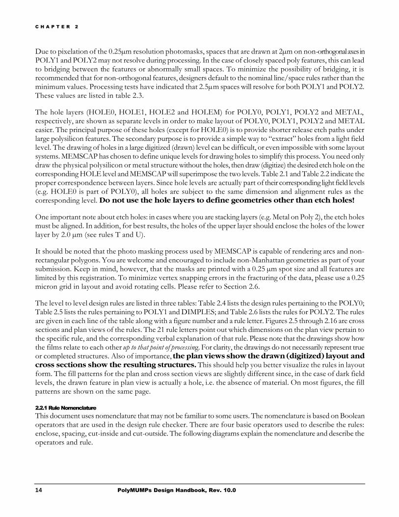
L1 to L2 cut inside (Figure 2.3). This operator defines the amount that a layer 2 feature can traverse layer 1. The cut-in has an associated minimum value, C.
FIGURE 2.3. Layer1 to Layer2 Cut-in. C = minimum cut-in dimension.
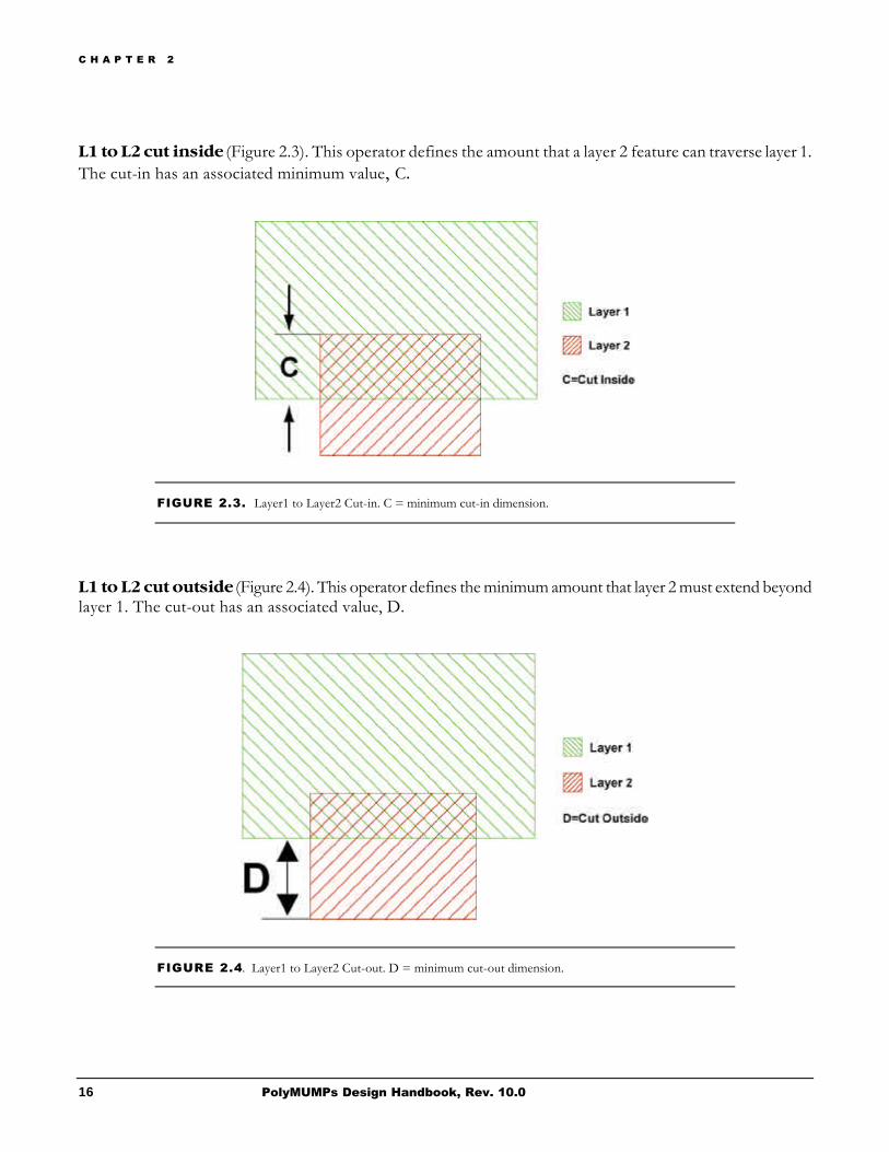
L1 to L2 cut outside (Figure 2.4). This operator defines the minimum amount that layer 2 must extend beyond layer 1. The cut-out has an associated value, D.
FIGURE 2.4. Layer1 to Layer2 Cut-out. D = minimum cut-out dimension.

P O L Y M U M P S D E S I G N G U I D E L I N E S A N D R U L E S
17 PolyMUMPs Design Handbook, Rev. 10.0
Table 2.4 contains the rules that relate to POLY0. The Poly 0 layer is typically used as a ground plane or for routing purposes. The use of this layer is optional, and may not be needed. Rules A and B ensure proper placement of ANCHOR1 with respect to POLY0. Rules C and D define proper enclosure of POLY1 and POLY2. Rules E and F ensure proper placement of ANCHOR2 with respect to POLY0.
Rule Rule Letter Figure # Min. Value (µm) POLY0 space to ANCHOR1 A 2.5 4.0 POLY0 enclose ANCHOR1 B 2.5 4.0 POLY0 enclose POLY1 C 2.6 4.0 POLY0 enclose POLY2 D 2.7 5.0 POLY0 enclose ANCHOR2 E 2.8 5.0 POLY0 space to ANCHOR2 F 2.8 5.0
TABLE 2.4. POLY0 Rules
2.2.2 POLY1 and DIMPLES Table 2.5 lists all the rules pertaining to POLY1 and DIMPLE. Rules G and N assure that the POLY1 level provides sufficient coverage of lower levels. Rule H ensures that subsequent Poly 2 structures are adequately connected to Poly 1. Rule O is a special case rule explained in more detail below. Rule K ensures that Poly 1 and 2 will not be shorted due to misalignment of the anchor hole. Rule R ensures that the sacrificial oxide is etched from under large polysilicon features before the metal is etched away.
Rule O applies to the special case where a Poly 2 structure overlaps Poly1 completely on one side but does not extend entirely over the other side. To avoid lithography and etch problems the edges of Poly 1 and Poly 2 should be separated by a minimum of 4.0µm (see Figure 2.14). This rule only applies when the designer does NOT want POLY2 to completely enclose POLY1. In the case where it is desirable to have POLY2 completely enclose POLY1, refer to rule Q.
Rule Rule Letter Figure # Min. Value (µm) POLY1 enclose ANCHOR1 G 2.6 4.0 POLY1 enclose DIMPLE N 2.13 4.0 POLY1 enclose POLY1_POLY2_VIA H 2.9, 2.11 4.0 POLY1 enclose POLY2 O 2.14 4.0 POLY1 space to ANCHOR2 K 2.11 3.0 *Lateral etch holes space in POLY1 R 2.15 =30 (max. value)
TABLE 2.5. POLY1 and DIMPLE Rules
2.2.3 POLY2 Table 2.6 lists the rules that relate to POLY2. Rules J and L ensure that the Poly 2 properly overlaps anchor and via holes. Rules P and Q pertain to proper overlaps of Poly 1 and Poly 2 relative to each other. Rule M ensures that Metal does not overlap Poly 2. (Users who want extend Metal beyond a Poly 2 pad should be aware that step coverage at the Poly 2 edge is poor and may result in mechanical failure and high electrical resistance at the step.) Rule I defines the minimum space between Poly 1 and 2 to assure good delineation and avoid shorting. Rule T defines the necessary enclosure of HOLE2 around HOLE1 in the special case where Poly 1 and Poly 2 layers overlap and both must be released. Rule U defines the minimum enclosure of HOLEM around HOLE2 to

C H A P T E R 2
18 PolyMUMPs Design Handbook, Rev. 10.0
ensure that the holes are properly aligned for release. As with POLY1, the last rule guarantees release of large polysilicon micro-structures.
As mentioned above, rule T applies to the special case where a stack of Poly 1 and Poly 2 must be released. To best facilitate release of the structures, etch holes in both layers (HOLE1 and HOLE2) must be aligned and the size of the hole in Poly 2 should exceed the Poly 1 etch hole by 2µm, i.e. HOLE2 encloses HOLE1 by 2.0µm.
Rule Rule Letter Figure # Min. Value (µm)
POLY2 enclose ANCHOR2 J 2.7,2.10 5.0 POLY2 enclose POLY1_POLY2_VIA L 2.9 4.0 POLY2 cut-in POLY1 P 2.14 5.0 POLY2 cut-out POLY1 Q 2.14 4.0 POLY2 enclose METAL M 2.12 3.0 POLY2 space to POLY1 I 2.10 3.0 HOLE2 enclose HOLE1 T 2.16 2.0 HOLEM enclose HOLE2 U 2.16 2.0 *Lateral etch holes space in POLY2 S 2.15 =30 (max. value)
TABLE 2.6. POLY2 and Etch Holes Rules
Table 2.7 and the figures on pages 19-30 provide details of the different layer rules.
Level 1 Level 2 Min. Feature
Min. Spacing
Enclose Spacing Cut- In Cut- Out
- 2 2 ANCHOR1 4/B/2.5 4/A/2.5 POLY1 4/C/2.6 ANCHOR2 5/E/2.8 5/F/2.8
POLY0
POLY2 5/D/2.7 - 2 2 / 2.52
POLY0 ANCHOR1 4/G/2.6 ANCHOR2 3/K/2.11 POLY2 4/0/2.14 DIMPLE 4/N/2.13
POLY1
POLY1_POLY2_VIA 4/H/2.9 - 2 2 / 2.52
POLY0 POLY1 3/I/2.10 5/P/2.14 4/Q/2.14 VIA 4/L/2.9 ANCHOR2 5/J/2.7
POLY2
METAL 3/M/2.12 HOLEM HOLE2 2/U/2.16 HOLE2 HOLE1 2/T/2.16
TABLE 2.7. PolyMUMPs design rule reference sheet. Table shows minimum dimensions (µm), rule name, and figure number, respectively.
2 Use 2nd number for non-orthogonal spaces due to pixelation of the photomask
P O L Y M U M P S D E S I G N G U I D E L I N E S A N D R U L E S
19 PolyMUMPs Design Handbook, Rev. 10.0
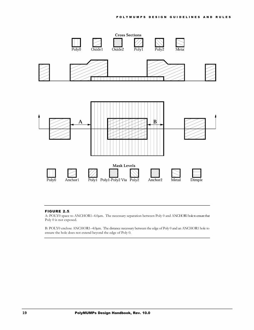
FIGURE 2.5. A: POLY0 space to ANCHOR1–4.0µm. The necessary separation between Poly 0 and ANCHOR1 hole to ensure that Poly 0 is not exposed. B: POLY0 enclose ANCHOR1–4.0µm. The distance necessary between the edge of Poly 0 and an ANCHOR1 hole to ensure the hole does not extend beyond the edge of Poly 0.
C H A P T E R 2
20 PolyMUMPs Design Handbook, Rev. 10.0
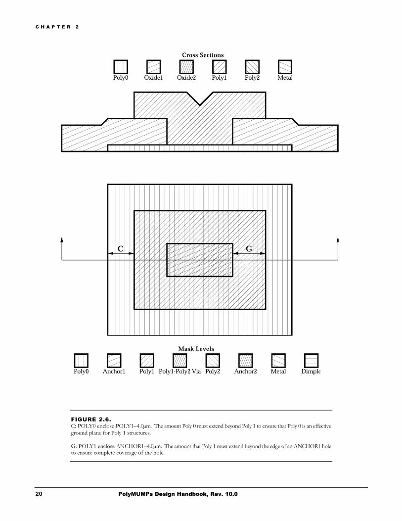
FIGURE 2.6. C: POLY0 enclose POLY1–4.0µm. The amount Poly 0 must extend beyond Poly 1 to ensure that Poly 0 is an effective ground plane for Poly 1 structures. G: POLY1 enclose ANCHOR1–4.0µm. The amount that Poly 1 must extend beyond the edge of an ANCHOR1 hole to ensure complete coverage of the hole.

P O L Y M U M P S D E S I G N G U I D E L I N E S A N D R U L E S
21 PolyMUMPs Design Handbook, Rev. 10.0
FIGURE 2.7. D: POLY0 enclose POLY2–5.0µm. The amount Poly 0 must extend beyond the edge of a Poly 2 structure to ensure that Poly 0 is an effective ground plane. J: POLY2 enclose ANCHOR2–5.0µm. The amount Poly 2 must extend beyond an ANCHOR2 hole to ensure complete coverage of the hole.
C H A P T E R 2
22 PolyMUMPs Design Handbook, Rev. 10.0
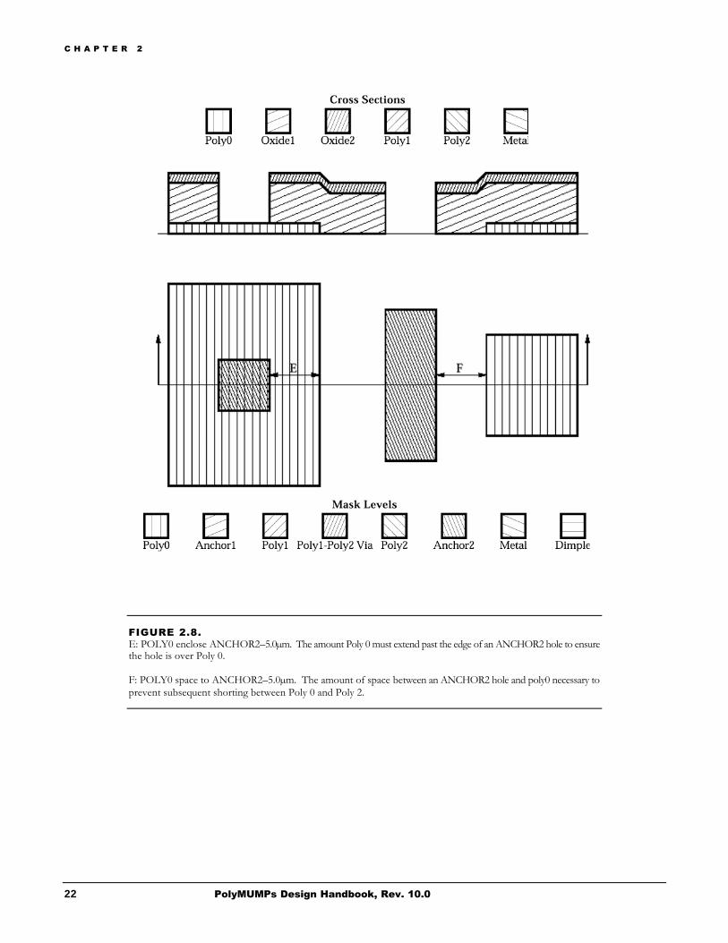
FIGURE 2.8. E: POLY0 enclose ANCHOR2–5.0µm. The amount Poly 0 must extend past the edge of an ANCHOR2 hole to ensure the hole is over Poly 0. F: POLY0 space to ANCHOR2–5.0µm. The amount of space between an ANCHOR2 hole and poly0 necessary to prevent subsequent shorting between Poly 0 and Poly 2.

P O L Y M U M P S D E S I G N G U I D E L I N E S A N D R U L E S
23 PolyMUMPs Design Handbook, Rev. 10.0
FIGURE 2.9. H: POLY1 enclose POLY1_POLY2_VIA–4.0µm. The distance between the POLY1_POLY2_VIA hole and the edge of Poly 1 necessary to ensure the via hole is entirely over Poly 1. L: POLY2 enclose POLY1_POLY2_VIA–4.0µm. The amount Poly 2 must extend beyond the POLY1_POLY2_VIA hole to ensure complete coverage of the hole.
C H A P T E R 2
24 PolyMUMPs Design Handbook, Rev. 10.0
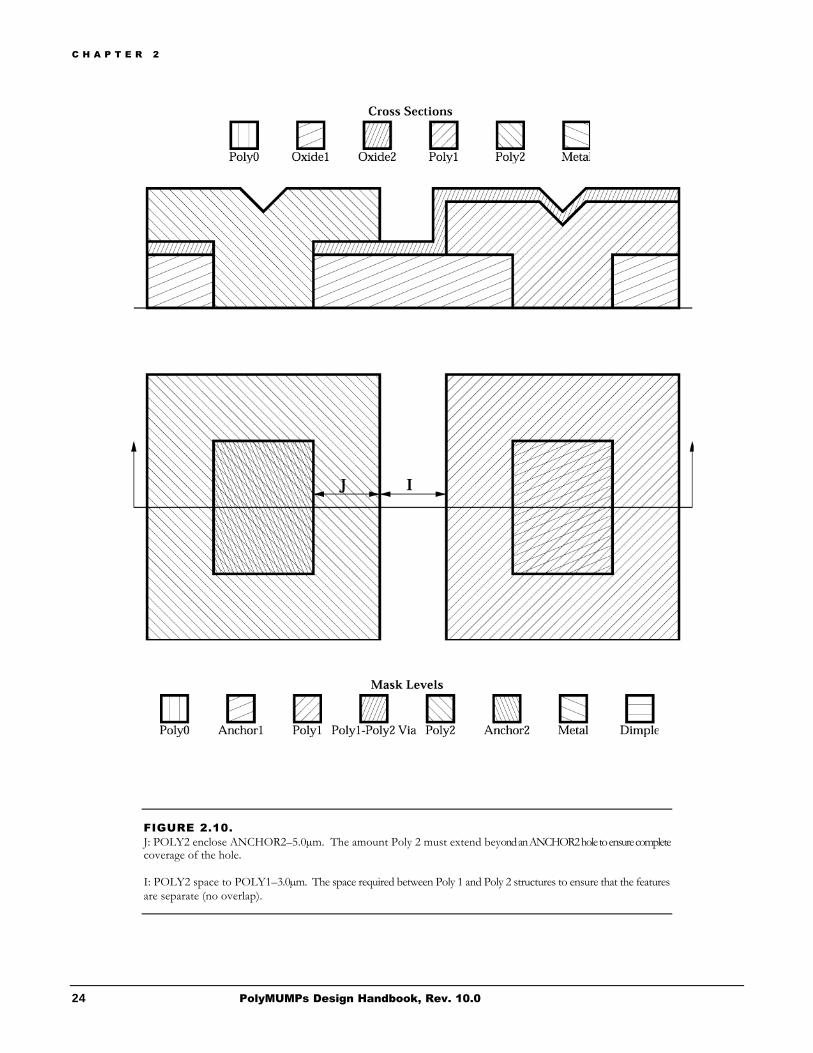
FIGURE 2.10. J: POLY2 enclose ANCHOR2–5.0µm. The amount Poly 2 must extend beyond an ANCHOR2 hole to ensure complete coverage of the hole. I: POLY2 space to POLY1–3.0µm. The space required between Poly 1 and Poly 2 structures to ensure that the features are separate (no overlap).

P O L Y M U M P S D E S I G N G U I D E L I N E S A N D R U L E S
25 PolyMUMPs Design Handbook, Rev. 10.0
FIGURE 2.11. K: POLY1 space to ANCHOR2–3.0µm. The space between a Poly 1 structure and an ANCHOR2 hole necessary to avoid subsequent Poly 1–Poly 2 contact. H: POLY1 enclose POLY1_POLY2_VIA–4.0µm. The distance between the POLY1_POLY2_VIA hole and the edge of Poly 1 necessary to ensure the via hole is entirely over Poly 1. Poly0 Oxide1 Oxide2 Poly1 Poly2 Metal
C H A P T E R 2
26 PolyMUMPs Design Handbook, Rev. 10.0
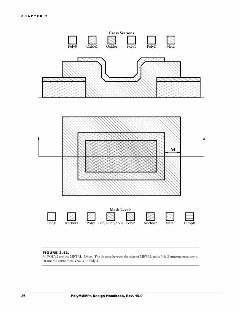
FIGURE 2.12. M: POLY2 enclose METAL–3.0µm. The distance between the edge of METAL and a Poly 2 structure necessary to ensure the entire metal area is on Poly 2.

P O L Y M U M P S D E S I G N G U I D E L I N E S A N D R U L E S
27 PolyMUMPs Design Handbook, Rev. 10.0
FIGURE 2.13. N: POLY1 enclose DIMPLE–4.0µm. The amount POLY1 must extend beyond the edge of DIMPLE to ensure the dimple is completely covered by Poly1.

C H A P T E R 2
28 PolyMUMPs Design Handbook, Rev. 10.0
FIGURE 2.14. P: POLY2 cut-in POLY1–5.0µm. The minimum amount Poly 2 must extend over a Poly 1 structure to ensure overlap. O: POLY1 enclose POLY2–4.0µm. The minimum distance from the edge of Poly 1 to Poly 2 necessary to ensure the Poly 2 does not overlap the Poly 1 edge. Q: POLY2 cut-out POLY1–4.0µm. The minimum distance Poly 2 must extend beyond the Poly1 edge to ensure complete edge overlap.
P O L Y M U M P S D E S I G N G U I D E L I N E S A N D R U L E S
29 PolyMUMPs Design Handbook, Rev. 10.0
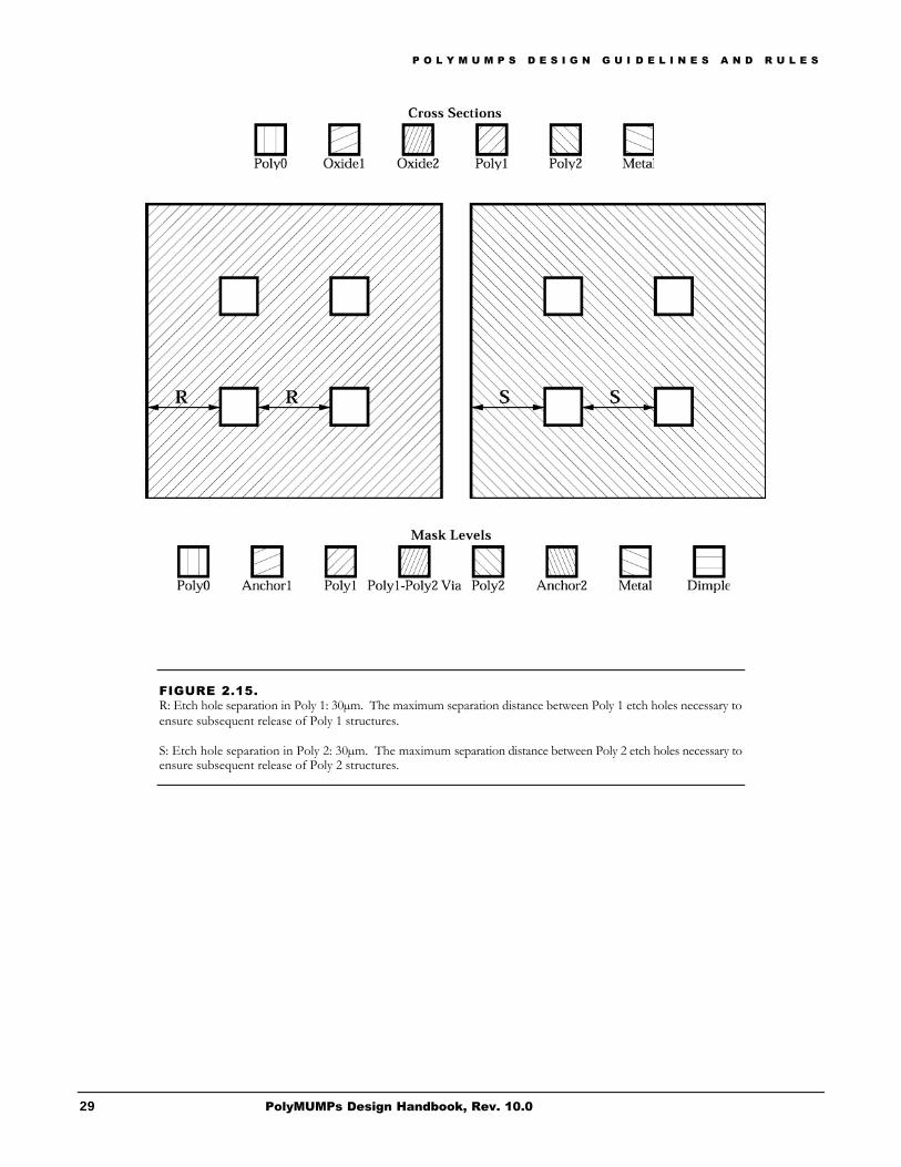
FIGURE 2.15. R: Etch hole separation in Poly 1: 30µm. The maximum separation distance between Poly 1 etch holes necessary to ensure subsequent release of Poly 1 structures. S: Etch hole separation in Poly 2: 30µm. The maximum separation distance between Poly 2 etch holes necessary to ensure subsequent release of Poly 2 structures.

C H A P T E R 2
30 PolyMUMPs Design Handbook, Rev. 10.0
FIGURE 2.16. T: HOLE2 enclose HOLE1–2.0µm. The necessary border of HOLE2 around HOLE1 to ensure good release results. U: HOLEM enclose HOLE2–2.0µm. The necessary border of HOLEM around HOLE2 to ensure good release results.

P O L Y M U M P S D E S I G N G U I D E L I N E S A N D R U L E S
31 PolyMUMPs Design Handbook, Rev. 10.0
2.3 Beyond the Design Rules Section 2.3 is highly recommended reading for any PolyMUMPs user, novice or experienced. It includes several common design errors that warrant extended discussion based on observations from previous PolyMUMPs runs. This section also contains guidelines for several processing methods that may be of interest
This section is based upon the experience MEMSCAP has gained working with many groups of people, both novices and experts in the area of MEMS. Below are some of the more common errors made in designing surface micromachined MEMS along with some helpful hints.
2.3.1 Layout convention This was covered in section 2.2 but will be reiterated here. The convention used by the PolyMUMPs processes in defining mask levels is simple. For all polysilicon levels and the metal level (POLY0, POLY1, POLY2 and METAL) the masks are light field. For these levels, draw (i.e. digitize) the polysilicon (or metal) feature you want to keep. All oxide levels and hole levels (DIMPLE, ANCHOR1, ANCHOR2, POLY1_POLY2_VIA and HOLE0,1,2,M) are dark field. For these levels, draw the hole you want to make. It is imperative that these conventions be followed for your devices to be fabricated correctly.
2.3.2 Don’t put a hole where you don’t need it. The PolyMUMPs process has three levels for making polysilicon connections and anchors–ANCHOR1, ANCHOR2 and POLY1_POLY2_VIA. The purpose of these levels is outlined in Table 2.2. An error made frequently by beginning users is to place oxide holes where they are not needed (i.e. to not fill a hole with polysilicon). This detrimentally affects the device in two distinct ways. First, stringers may form inside the anchor holes when removing the polysilicon. Second, and more importantly, the underlying layers are exposed to unnecessary etching that can thin or remove them altogether.
The following example illustrates the effect of not adequately covering ANCHOR1 holes with POLY1. Figure 2.17 shows ANCHOR1 holes etched down to both Poly 0 and Nitride. Some of the Nitride is removed in the overetch of the ANCHOR1 holes. Figure 2.18 shows the same anchor holes after the Poly 1 layer has been etched. In this case, the ANCHOR1 holes are not entirely covered by Poly 1 and the underlying layers are attacked further. The Nitride layer is thinned to the point where shorting to the substrate can occur and the exposed Poly 0 is completely removed resulting in unintentional isolation of Poly 0 structures. In addition, a 4 to 4.5µm step has been produced which complicates lithography at subsequent steps.
FIGURE 2.17. ANCHOR1 cuts down to Nitride and Poly 0. Note that the underlying Nitride has been partially etched (see fig. 1.1 for fill patterns).
C H A P T E R 2
32 PolyMUMPs Design Handbook, Rev. 10.0
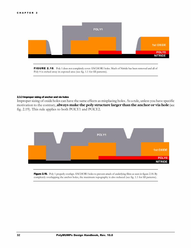
FIGURE 2.18 . Poly 1 does not completely cover ANCHOR1 holes. Much of Nitride has been removed and all of Poly 0 is etched away in exposed area (see fig. 1.1 for fill patterns).
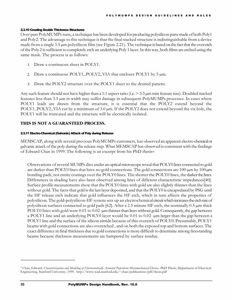
2.3.3 Improper sizing of anchor and via holes Improper sizing of oxide holes can have the same effects as misplacing holes. As a rule, unless you have specific motivation to the contrary, always make the poly structure larger than the anchor or via hole (see fig. 2.19). This rule applies to both POLY1 and POLY2.
Figure 2.19. Poly 1 properly overlaps ANCHOR1 holes to prevent attack of underlying films as seen in figure 2.18. By completely overlapping the anchor holes, the maximum topography is also reduced (see fig. 1.1 for fill patterns).

P O L Y M U M P S D E S I G N G U I D E L I N E S A N D R U L E S
33 PolyMUMPs Design Handbook, Rev. 10.0
2.3.4 Improper pad design The failure to heed enclosure rules when designing probe pads can result in a number of problems. Some users have experienced shorting of their devices to the substrate as a result of thinned or breached Nitride directly adjacent to pads. If the Poly 0 is used for routing and the ANCHOR1 holes are not enclosed by POLY1, the Poly 0 line will be cut by the Poly 1 etch. To avoid these and other problems, the standard pad shown in figure 2.20, should be used. This pad design can be requested free of charge as either a CIF or GDSII® file from MEMSCAP' MEMS WWW page.
FIGURE 2.20 Example of proper pad design. The fill patterns from outside to inside are POLY0, POLY1, ANCHOR1 and POLY2 (superimposed), POLY1_POLY2_VIA, and METAL.
2.3.5 Improper use of ANCHOR1 plus POLY1_POLY2_VIA A common error made by beginning users is to combine ANCHOR1 and POLY1_POLY2_VIA to provide anchor holes to the substrate layers for Poly 2. This combination of etches provides anchor holes but it also has the effect of leaving the substrate layers exposed as described in section 2.3.2. Furthermore, any misalignment between POLY1_POLY2_VIA and ANCHOR1 will detrimentally affect the Poly 2 structure that is being

C H A P T E R 2
34 PolyMUMPs Design Handbook, Rev. 10.0
fabricated. To avoid these problems, always use ANCHOR2 for anchoring Poly 2 to the substrate layers.
2.3.6 Metal The use of metal is dictated by the availability of an exposed structural surface and the conformality of the film over steps. The metal layer is best suited atop Poly 2 because it provides an oxide free surface. Under some conditions, the metal can be placed directly on the Second Oxide but this can lead to problems upon release.
The other controlling factor of the metal layer is step coverage. The metal layer, a thin adhesion layer of chromium and 0.5 µm of gold, is evaporated and patterned by lift-off. Because evaporation does not provide good conformality over large steps, the electrical and mechanical connection over these steps is poor. Upon release, metal lines over Poly 2 steps often fail or produce very high resistances. As such, MEMSCAP recommends that metal be deposited directly atop Poly 2 only. When metal is necessary for low resistance routing, MEMSCAP recommends that Poly 2 lines be anchored to the Nitride by ANCHOR2 cuts and the Metal be placed atop the Poly 2 lines.
2.3.7 Nominal design rule It is worth noting that the term “minimum” size is used to denote the absolute smallest feature or space you should consider in your design. Our ability to print very small features is dependent upon film reflectivity, proximity effects, topography, photoresist planarization and etch bias. For this reason, we suggest that you adhere to the 3 µm nominal design rule stated in Table 2.3. This will provide greater process latitude during fabrication and greatly improve the outcome of your project.
Obviously there are performance benefits from smaller features and spaces (e.g. resonators). In cases where the 2 µm design rule is especially beneficial, the designer may choose to use the minimum. However, avoid using long (>30 µm) isolated 2 µm lines in POLY0, POLY1 or POLY2. Proximity effects and polysilicon reflectivity make such features difficult to lithographically image without compromising the lithography quality on the rest of the wafer. If you feel this kind of structure is necessary for your devices to function, please discuss this with MEMSCAP early in the design phase.
2.3.8 Minimum dimension exceptions from Table 2.3 In cases where it is absolutely necessary to have an ANCHOR1 or ANCHOR2 hole from which all poly must be removed, there is an adjustment to the rules that helps minimize the stringer and topography problems that can be caused. For the case of an ANCHOR1 hole requiring removal of all Poly 1, the minimum hole size is 5.0 µm rather than 3.0 µm. For an ANCHOR2 hole requiring removal of all Poly 2, the minimum hole size is also 5.0 µm rather than 3.0 µm.
2.3.9 Breaching the Nitride In some cases it is desirable to breach the nitride layer, particularly when the device must be grounded through the substrate. Just as section 2.3.2 explains the dangers of this, there are situations where it is desirable. There are several oxide etch combinations that will accomplish this. However, based on empirical results, the optimum combination3 (i.e. lowest contact resistance) is ANCHOR1 plus POLY1_POLY2_VIA (and removing the Poly 1). The anchor hole can then be filled with Poly 2 to provide a ground to substrate connection.
THIS IS NOT A GUARANTEED PROCESS.
3 Run to run variation can lead to problems making contact with this combination. An alternative is the combination of ANCHOR1, POLY1_POLY2_VIA, and ANCHOR2. This may lead to higher contact resistance but gives a higher probability of substrate contact. (MEMSCAP does not guarantee this process feature)
P O L Y M U M P S D E S I G N G U I D E L I N E S A N D R U L E S
35 PolyMUMPs Design Handbook, Rev. 10.0
2.3.10 Creating Double Thickness Structures Over past PolyMUMPs runs, a technique has been developed for producing polysilicon parts made of both Poly1 and Poly2. The advantage to this technique is that the final stacked structure is indistinguishable from a device made from a single 3.5 µm polysilicon film (see Figure 2.21). The technique is based on the fact that the over-etch of the Poly 2 is sufficient to completely etch an underlying Poly 1 layer. In this way, both films are etched using the same mask. The process is as follows:
1. Draw a continuous sheet in POLY1.
2. Draw a continuous POLY1_POLY2_VIA that encloses POLY1 by 5 µm.
3. Draw the POLY2 structure over the POLY1 sheet to the desired pattern.
Any such feature should not have higher than a 1:1 aspect ratio (i.e. > 3.5 µm min feature size). Doubled stacked features less than 3.5 µm in width may suffer damage in subsequent PolyMUMPs processes. In cases where POLY1 leads are drawn from the structure, it is essential that the POLY2 extend beyond the POLY1_POLY2_VIA cut by a minimum of 3.0 µm. If the POLY2 does not extend beyond the via hole, the POLY1 will be truncated and the structure will be electrically isolated.
THIS IS NOT A GUARANTEED PROCESS.
2.3.11 Electro-Chemical (Galvanic) Attack of Poly during Release MEMSCAP, along with several previous PolyMUMPs customers, has observed an apparent electro-chemical or galvanic attack of the poly during the release step. What MEMSCAP has observed is consistent with the findings of Edward Chan in 1999. The following is an excerpt from his PhD thesis4:
Observations of several MUMPs dies under an optical microscope reveal that POLY0 lines connected to gold are darker than POLY0 lines that have no gold connections. The gold connections are 100-µm by 100-µm bonding pads, not entire coatings over the POLY0 lines. The shorter the POLY0 lines, the darker the lines. Differences in shading have also been observed among lines of different characteristic impedances[40]. Surface profile measurements show that the POLY0 lines with gold are also slightly thinner than the lines without gold. The facts that gold is the last layer deposited, and that the POLY0 is encapsulated by PSG until the HF release etch indicate that gold influences the HF etch, which in turn affects the properties of polysilicon. The gold-polysilicon-HF system sets up an electrochemical circuit which increases the etch rate of polysilicon surfaces connected to gold pads [62]. After a 2.5 minute HF etch, the nominally 0.5-µm thick POLY0 lines with gold were 0.01 to 0.02 -µm thinner than lines without gold. Consequently, the gap between a POLY1 line and an underlying POLY0 layer would be 0.01 to 0.02 -µm larger than the gap between a POLY1 line and the surface of the silicon nitride because of this overetch of POLY0. Presumably, POLY1 beams with gold connections are also overetched , and on both the exposed top and bottom surfaces. The exact difference in final thickness due to gold connections is more difficult to determine among freestanding beams because thickness measurements are hampered by surface residue.
4 Chan, Edward, Characterization and Modeling of Electrostatically Actuated Polysilicon Micromechanical Devices. PhD Thesis, Department of Electrical Engineering, Stanford University, 1999. http://www-tcad.stanford.edu/~chan/publications/pdf/thesis.pdf
C H A P T E R 2
36 PolyMUMPs Design Handbook, Rev. 10.0
Subsequent observations also indicate a correlation between the surface area of gold attached to an electrical node and the surface area of the Poly 0. At this time it is unclear whether this attack takes place during the release step while the sample is in 49% HF or while the sample is being rinsed in DI after the dip in HF. This etching of the poly has not been observed in the absence of a metal layer.
CUSTOMERS SHOULD BE AWARE OF THIS PHENOMENON WHEN DESIGNING FOR POLYMUMPS. MEMSCAP CANNOT BE HELD RESPONSIBLE FOR THE IMPACT OF GALVANIC ATTACK.
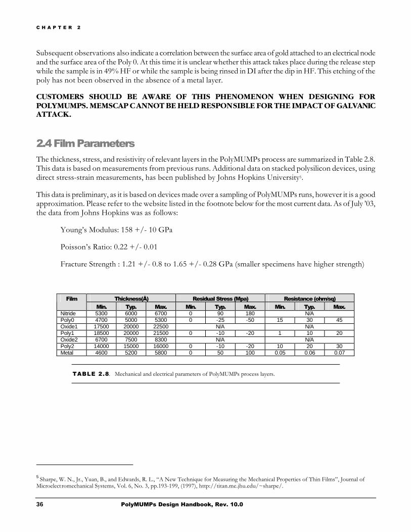
2.4 Film Parameters The thickness, stress, and resistivity of relevant layers in the PolyMUMPs process are summarized in Table 2.8. This data is based on measurements from previous runs. Additional data on stacked polysilicon devices, using direct stress-strain measurements, has been published by Johns Hopkins University5.
This data is preliminary, as it is based on devices made over a sampling of PolyMUMPs runs, however it is a good approximation. Please refer to the website listed in the footnote below for the most current data. As of July ’03, the data from Johns Hopkins was as follows:
Young’s Modulus: 158 +/- 10 GPa
Poisson’s Ratio: 0.22 +/- 0.01
Fracture Strength : 1.21 +/- 0.8 to 1.65 +/- 0.28 GPa (smaller specimens have higher strength)
Thickness(Å) Residual Stress (Mpa) Resistance (ohm/sq) Film Min. Typ. Max. Min. Typ. Max. Min. Typ. Max.
Nitride 5300 6000 6700 0 90 180 N/A Poly0 4700 5000 5300 0 -25 -50 15 30 45 Oxide1 17500 20000 22500 N/A N/A Poly1 18500 20000 21500 0 -10 -20 1 10 20 Oxide2 6700 7500 8300 N/A N/A Poly2 14000 15000 16000 0 -10 -20 10 20 30 Metal 4600 5200 5800 0 50 100 0.05 0.06 0.07
TABLE 2.8. Mechanical and electrical parameters of PolyMUMPs process layers.
5 Sharpe, W. N., Jr., Yuan, B., and Edwards, R. L., “A New Technique for Measuring the Mechanical Properties of Thin Films”, Journal of Microelectromechanical Systems, Vol. 6, No. 3, pp.193-199, (1997), http://titan.me.jhu.edu/~sharpe/.

P O L Y M U M P S D E S I G N G U I D E L I N E S A N D R U L E S
37 PolyMUMPs Design Handbook, Rev. 10.0
FIGURE 2.21. Design of double thickness structures. The upper figure shows the cross section of the structure after the Poly 2 has been deposited and etched (but before release).

C H A P T E R 2
38 PolyMUMPs Design Handbook, Rev. 10.0
2.5 EZ-PolyMUMPs Design Rules For those participants inexperienced in the intricacies of process design, rule interactions, or even those who are experienced but who really don’t need to push the design envelope for their designs, we recommend the EZ-PolyMUMPs rules. If you make all minimum geometries ≥ 5.0 µm (lines and spaces), and all overlaps and borders ≥ 5.0 µm, you will easily meet all the aforementioned design rules and you minimize any potential process design interactions. (Please note that the etch hole spacings, rules R and S, must still be ≤ 30.0 µm).
2.6 Layout Requirements 2.6.1 Usable Area The maximum allowed design area for PolyMUMPs is 1cm x 1cm. Care should be taken to avoid placing structures closer than 100µm from the edge of the die since dicing can occasionally damage the edge of the chip. It is required that you leave the 550µm x 300µm (x and y dimensions, respectively) rectangle vacant in the lower left hand corner of your die. This space is used by MEMSCAP for a drop in test structure for post process evaluation of the run.
2.6.2 Cell Name Restrictions Some errors have occurred in the past due to nonstandard cell names. In order to reduce these errors and the time it takes to translate designs, some guidelines need to be put in place. They are as follows:
1). Cell names should be under 28 characters.
2). Cell names should consist of only the following characters or numerals [a-zA-Z0-9] and the underscore character ‘_’.
2.6.3 Layer Names Layouts must use layer names as indicated in Table 2.3. For CIF submissions the indicated names should be used (i.e. for POLY0 use CPZ) and for GDS submissions the correct number must be used. Other layers may be in the design; but, they will be ignored. MEMSCAP is not responsible for layers omitted due to failure to comply to naming conventions.
2.6.4 General Layout Tips and Known Software Bugs Mentor software is currently used to assemble the PolyMUMPs wafers. It does a reasonable job with most translations; however, there are some additional nuances of which users should be aware.
Keep in mind that these are the bugs that MEMSCAP is aware of - we are not responsible for problems resulting from other bugs not listed here.
1). Due to pixelation of the 0.25µm resolution photomasks, spaces that are drawn at 2µm on non-orthogonal axes in POLY1 and POLY2 may not resolve during processing. In the case of closely spaced poly features, this can lead to bridging between the features or abnormally small spaces. To minimize the possibility of bridging, it is recommended that for non-orthogonal features, designers default to the nominal line/space rules rather than the minimum values. Processing tests have indicated that 2.5µm spaces will resolve for both POLY1 and POLY2. These values are listed in table 2.3 of this handbook.

P O L Y M U M P S D E S I G N G U I D E L I N E S A N D R U L E S
39 PolyMUMPs Design Handbook, Rev. 10.0
2). In GDS, three wire types are allowed, extended, butted, and rounded ends. Rounded ended wires will be truncated. It is strongly suggested that only extended wire types be used with CIF files; otherwise, information may be lost and connections broken.
3). L-Edit versions 7 and 8, up until version 8.22, have a bug. The bug comes from the donut command in L-Edit which becomes a filled circle when written out to gds and translated into other programs. If you use a donut, be sure to use the horizontal or vertical cut commands to break the donut into multiple polygons.
4). There is a bug in L-Edit version 8.22 when working with rotated and mirrored instances. If an instance is rotated and mirrored, then saved to gds, the rotation angle will be rounded off to the nearest degree (i.e. An instance is rotated 22.2 degrees and then mirrored, after saving to gds and reading back in, the angle will be changed to 22 degrees. To avoid errors, the cell referencing this instance should be flattened.
5). Coventorware allows arrays of instances to be scaled. This creates errors during translation. To avoid errors, any arrays of instances used in Coventorware and then scaled by a factor other than 1 should be flattened before submission to MEMSCAP.
2.6.5 Design Rule Checking PLEASE NOTE THAT NO ERROR CHECKING WILL BE DONE ON YOUR DESIGN.
2.7 Layout Submission Designs may be submitted in GDSII® or CIF format only. Technology files for L-Edit®, Cadence®, and Mentor’s layout tool may be requested via email at [email protected].
Before submitting your design, you must complete the Design Submission Form on our website at http://www.memscap.com/memsrus/svcsdes.html. Once we have received your completed form, you will receive an email with instructions and access information to upload your file to our ftp site.
All designs must be uploaded no later than midnight Eastern Standard Time on the submission due date.
2.8 Custom Dicing, Releasing and Critical Point Drying MEMSCAP offers dicing, releasing and supercritical CO2 drying service to PolyMUMPs customers. In order to provide the best possible service, a set of rules has been established. Refer to the website for pricing information on any of these services.
2.8.1 Dicing The minimum cut allowed for a subdiced PolyMUMPs chip is 2.5 mm. This allows users to dice a single 1 cm x 1 cm die into 16 sub chips. Dicing streets must be drawn 150 µm wide in POLY0. Users are also required to complete a subdicing map – a blank copy will be provided by MEMSCAP. Releasing of subdiced PolyMUMPs chips is subject to additional cost due to the added complexity of handling small subdiced chips.
2.8.2 HF Release and Supercritical CO2 Drying MEMSCAP will perform a standard HF release designed to fully remove the sacrificial oxide from chips that have been designed with the proper etch hole spacing. Even after HF Release, device stiction is a common problem. One way to minimize this effect is to dry the chips after HF release by critical point drying in CO2. The minimum subdicing cut for these post-processes is 5 mm.