Embed Size (px)
Citation preview
Phase Locked Loop
Basics For
Frequency Synthesizer
Applications
FCW - March 2011
FCW
Sciences
Legal Issues
Copyright 2011, Frederick Weist. All rights reserved.
No part of this document may be copied or reproduced
in any manner without the express written permission
of the author.
Matlab is a registered trademark of The MathWorks, Inc., Natick,
MA 01760.
Genesys is a registered trademark of Agilent Technologies, Inc.,
Santa Clara, CA 95051.
Mathcad is a registered trademark of Parametric Technology
Corp., Needham, MA 02494.
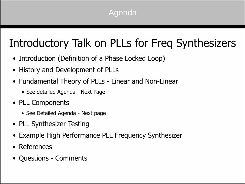
Agenda
Introductory Talk on PLLs for Freq Synthesizers
• Introduction (Definition of a Phase Locked Loop)
• History and Development of PLLs
• Fundamental Theory of PLLs - Linear and Non-Linear
• See detailed Agenda - Next Page
• PLL Components
• See Detailed Agenda - Next page
• PLL Synthesizer Testing
• Example High Performance PLL Frequency Synthesizer
• References
• Questions - Comments
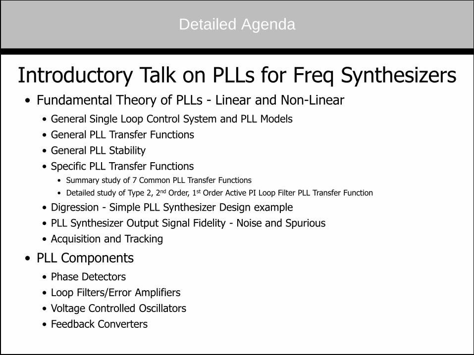
Detailed Agenda
Introductory Talk on PLLs for Freq Synthesizers
• Fundamental Theory of PLLs - Linear and Non-Linear
• General Single Loop Control System and PLL Models
• General PLL Transfer Functions
• General PLL Stability
• Specific PLL Transfer Functions
• Summary study of 7 Common PLL Transfer Functions
• Detailed study of Type 2, 2nd Order, 1st Order Active PI Loop Filter PLL Transfer Function
• Digression - Simple PLL Synthesizer Design example
• PLL Synthesizer Output Signal Fidelity - Noise and Spurious
• Acquisition and Tracking
• PLL Components
• Phase Detectors
• Loop Filters/Error Amplifiers
• Voltage Controlled Oscillators
• Feedback Converters
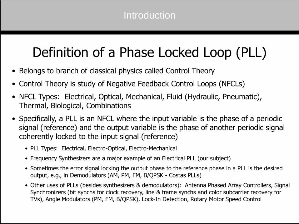
Introduction
Definition of a Phase Locked Loop (PLL)
• Belongs to branch of classical physics called Control Theory
• Control Theory is study of Negative Feedback Control Loops (NFCLs)
• NFCL Types: Electrical, Optical, Mechanical, Fluid (Hydraulic, Pneumatic), Thermal, Biological, Combinations
• Specifically, a PLL is an NFCL where the input variable is the phase of a periodic signal (reference) and the output variable is the phase of another periodic signal coherently locked to the input signal (reference)
• PLL Types: Electrical, Electro-Optical, Electro-Mechanical
• Frequency Synthesizers are a major example of an Electrical PLL (our subject)
• Sometimes the error signal locking the output phase to the reference phase in a PLL is the desired output, e.g., in Demodulators (AM, PM, FM, B/QPSK - Costas PLLs)
• Other uses of PLLs (besides synthesizers & demodulators): Antenna Phased Array Controllers, Signal Synchronizers (bit synchs for clock recovery, line & frame synchs and color subcarrier recovery for TVs), Angle Modulators (PM, FM, B/QPSK), Lock-In Detection, Rotary Motor Speed Control
Introduction
Definition of a Phase Locked Loop (PLL)
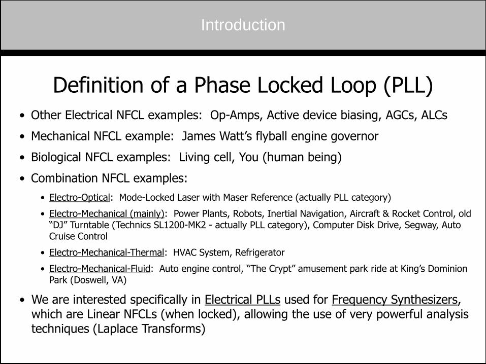
• Other Electrical NFCL examples: Op-Amps, Active device biasing, AGCs, ALCs
• Mechanical NFCL example: James Watt’s flyball engine governor
• Biological NFCL examples: Living cell, You (human being)
• Combination NFCL examples:
• Electro-Optical: Mode-Locked Laser with Maser Reference (actually PLL category)
• Electro-Mechanical (mainly): Power Plants, Robots, Inertial Navigation, Aircraft & Rocket Control, old “DJ” Turntable (Technics SL1200-MK2 - actually PLL category), Computer Disk Drive, Segway, Auto Cruise Control
• Electro-Mechanical-Thermal: HVAC System, Refrigerator
• Electro-Mechanical-Fluid: Auto engine control, “The Crypt” amusement park ride at King’s Dominion Park (Doswell, VA)
• We are interested specifically in Electrical PLLs used for Frequency Synthesizers, which are Linear NFCLs (when locked), allowing the use of very powerful analysis techniques (Laplace Transforms)
History
History and Development of PLLs
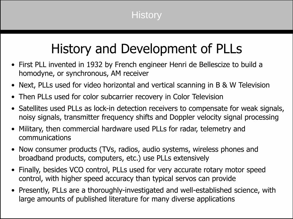
• First PLL invented in 1932 by French engineer Henri de Bellescize to build a homodyne, or synchronous, AM receiver
• Next, PLLs used for video horizontal and vertical scanning in B & W Television
• Then PLLs used for color subcarrier recovery in Color Television
• Satellites used PLLs as lock-in detection receivers to compensate for weak signals, noisy signals, transmitter frequency shifts and Doppler velocity signal processing
• Military, then commercial hardware used PLLs for radar, telemetry and communications
• Now consumer products (TVs, radios, audio systems, wireless phones and broadband products, computers, etc.) use PLLs extensively
• Finally, besides VCO control, PLLs used for very accurate rotary motor speed control, with higher speed accuracy than typical servos can provide
• Presently, PLLs are a thoroughly-investigated and well-established science, with large amounts of published literature for many diverse applications
Fundamental Theory of PLLs - Linear & Non-Linear
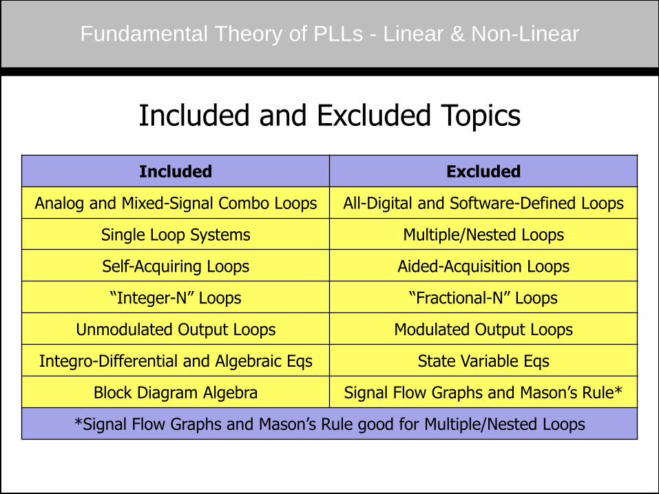
Included and Excluded Topics
Included Excluded
Analog and Mixed-Signal Combo Loops All-Digital and Software-Defined Loops
Single Loop Systems Multiple/Nested Loops
Self-Acquiring Loops Aided-Acquisition Loops
“Integer-N” Loops “Fractional-N” Loops
Unmodulated Output Loops Modulated Output Loops
Integro-Differential and Algebraic Eqs State Variable Eqs
Block Diagram Algebra Signal Flow Graphs and Mason’s Rule*
*Signal Flow Graphs and Mason’s Rule good for Multiple/Nested Loops
Fundamental Theory of PLLs - Linear & Non-Linear
Types of Analyses Used Here
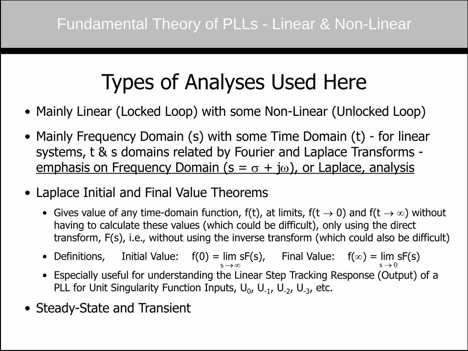
• Mainly Linear (Locked Loop) with some Non-Linear (Unlocked Loop)
• Mainly Frequency Domain (s) with some Time Domain (t) - for linear systems, t & s domains related by Fourier and Laplace Transforms - emphasis on Frequency Domain (s = s + jw), or Laplace, analysis
• Laplace Initial and Final Value Theorems
• Gives value of any time-domain function, f(t), at limits, f(t 0) and f(t ) without having to calculate these values (which could be difficult), only using the direct transform, F(s), i.e., without using the inverse transform (which could also be difficult)
• Definitions, Initial Value: f(0) = lim sF(s), Final Value: f() = lim sF(s)
• Especially useful for understanding the Linear Step Tracking Response (Output) of a PLL for Unit Singularity Function Inputs, U0, U-1, U-2, U-3, etc.
• Steady-State and Transient
s 0s
Fundamental Theory of PLLs - Linear & Non-Linear
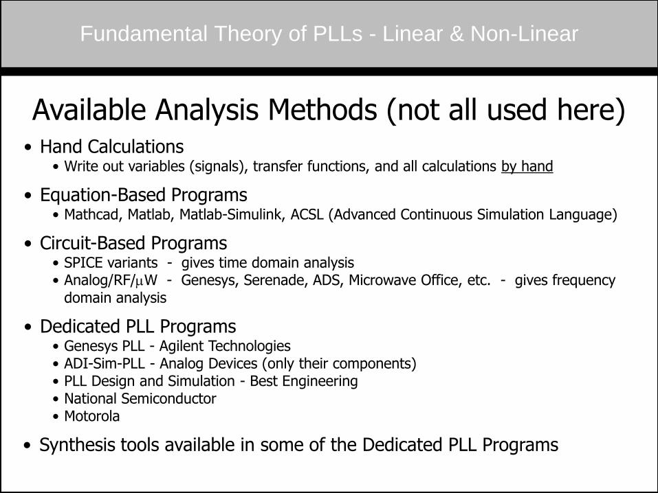
Available Analysis Methods (not all used here)
• Hand Calculations • Write out variables (signals), transfer functions, and all calculations by hand
• Equation-Based Programs • Mathcad, Matlab, Matlab-Simulink, ACSL (Advanced Continuous Simulation Language)
• Circuit-Based Programs • SPICE variants - gives time domain analysis • Analog/RF/mW - Genesys, Serenade, ADS, Microwave Office, etc. - gives frequency
domain analysis
• Dedicated PLL Programs • Genesys PLL - Agilent Technologies • ADI-Sim-PLL - Analog Devices (only their components) • PLL Design and Simulation - Best Engineering • National Semiconductor • Motorola
• Synthesis tools available in some of the Dedicated PLL Programs
Fundamental Theory of PLLs - Linear
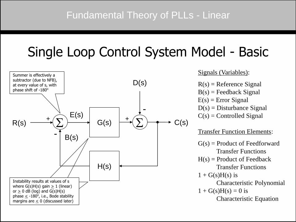
Single Loop Control System Model - Basic
B(s)
C(s)
D(s)
Signals (Variables):
R(s) = Reference Signal
B(s) = Feedback Signal
E(s) = Error Signal
D(s) = Disturbance Signal
C(s) = Controlled Signal
Transfer Function Elements:
G(s) = Product of Feedforward
Transfer Functions
H(s) = Product of Feedback
Transfer Functions
1 + G(s)H(s) is
Characteristic Polynomial
1 + G(s)H(s) = 0 is
Characteristic Equation
Summer is effectively a subtractor (due to NFB), at every value of s, with phase shift of -180o
Instability results at values of s where G(s)H(s) gain > 1 (linear) or > 0 dB (log) and G(s)H(s) phase < -180o, i.e., Bode stability margins are < 0 (discussed later)
S S E(s)
G(s)
H(s)
R(s)
-
+ +
-
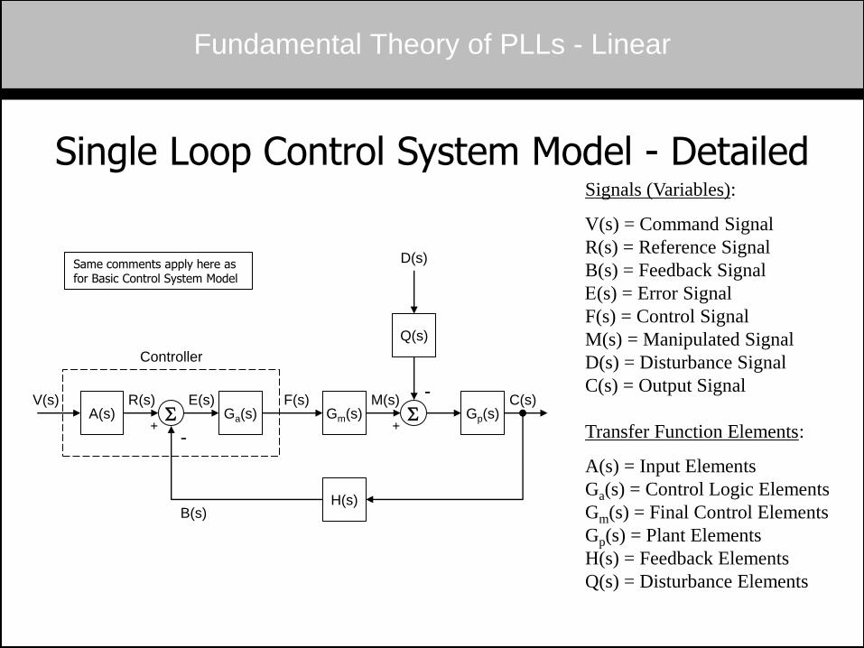
Single Loop Control System Model - Detailed Signals (Variables):
V(s) = Command Signal
R(s) = Reference Signal
B(s) = Feedback Signal
E(s) = Error Signal
F(s) = Control Signal
M(s) = Manipulated Signal
D(s) = Disturbance Signal
C(s) = Output Signal
Transfer Function Elements:
A(s) = Input Elements
Ga(s) = Control Logic Elements
Gm(s) = Final Control Elements
Gp(s) = Plant Elements
H(s) = Feedback Elements
Q(s) = Disturbance Elements
Fundamental Theory of PLLs - Linear
A(s)
H(s)
Gp(s)
Q(s)
Gm(s) Ga(s) S S
V(s) R(s) E(s) M(s) F(s) C(s)
B(s)
D(s)
Controller
+ -
+
-
Same comments apply here as for Basic Control System Model
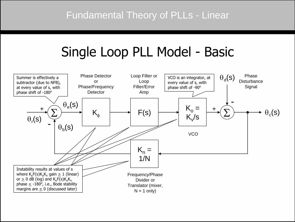
Single Loop PLL Model - Basic
qb(s)
Phase Detector
or
Phase/Frequency
Detector
Loop Filter or
Loop
Filter/Error
Amp
Frequency/Phase
Divider or
Translator (mixer,
N = 1 only)
Phase
Disturbance
Signal
Instability results at values of s where KfF(s)KoKn gain > 1 (linear) or > 0 dB (log) and KfF(s)KoKn phase < -180o, i.e., Bode stability margins are < 0 (discussed later)
Summer is effectively a subtractor (due to NFB), at every value of s, with phase shift of -180o
qe(s)
S S Ko =
Kv/s
F(s) Kf
Kn =
1/N
VCO
qd(s)
qc(s) qr(s)
+ -
+
-
Fundamental Theory of PLLs - Linear
VCO is an integrator, at every value of s, with phase shift of -90o
Fundamental Theory of PLLs - Linear
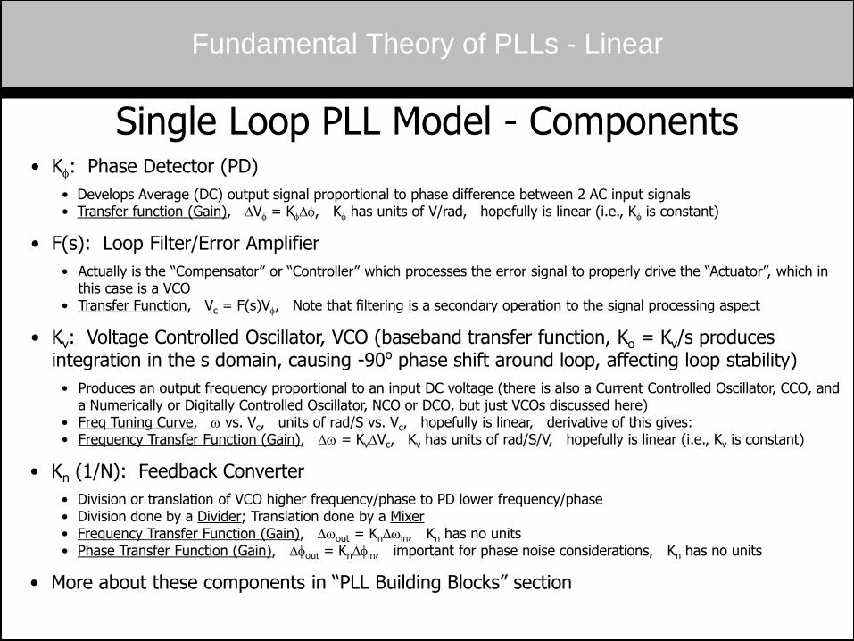
Single Loop PLL Model - Components
• Kf: Phase Detector (PD)
• Develops Average (DC) output signal proportional to phase difference between 2 AC input signals • Transfer function (Gain), DVf = KfDf, Kf has units of V/rad, hopefully is linear (i.e., Kf is constant)
• F(s): Loop Filter/Error Amplifier
• Actually is the “Compensator” or “Controller” which processes the error signal to properly drive the “Actuator”, which in this case is a VCO
• Transfer Function, Vc = F(s)Vf, Note that filtering is a secondary operation to the signal processing aspect
• Kv: Voltage Controlled Oscillator, VCO (baseband transfer function, Ko = Kv/s produces integration in the s domain, causing -90o phase shift around loop, affecting loop stability)
• Produces an output frequency proportional to an input DC voltage (there is also a Current Controlled Oscillator, CCO, and a Numerically or Digitally Controlled Oscillator, NCO or DCO, but just VCOs discussed here)
• Freq Tuning Curve, w vs. Vc, units of rad/S vs. Vc, hopefully is linear, derivative of this gives: • Frequency Transfer Function (Gain), Dw = KvDVc, Kv has units of rad/S/V, hopefully is linear (i.e., Kv is constant)
• Kn (1/N): Feedback Converter
• Division or translation of VCO higher frequency/phase to PD lower frequency/phase • Division done by a Divider; Translation done by a Mixer • Frequency Transfer Function (Gain), Dwout = KnDwin, Kn has no units • Phase Transfer Function (Gain), Dfout = KnDfin, important for phase noise considerations, Kn has no units
• More about these components in “PLL Building Blocks” section
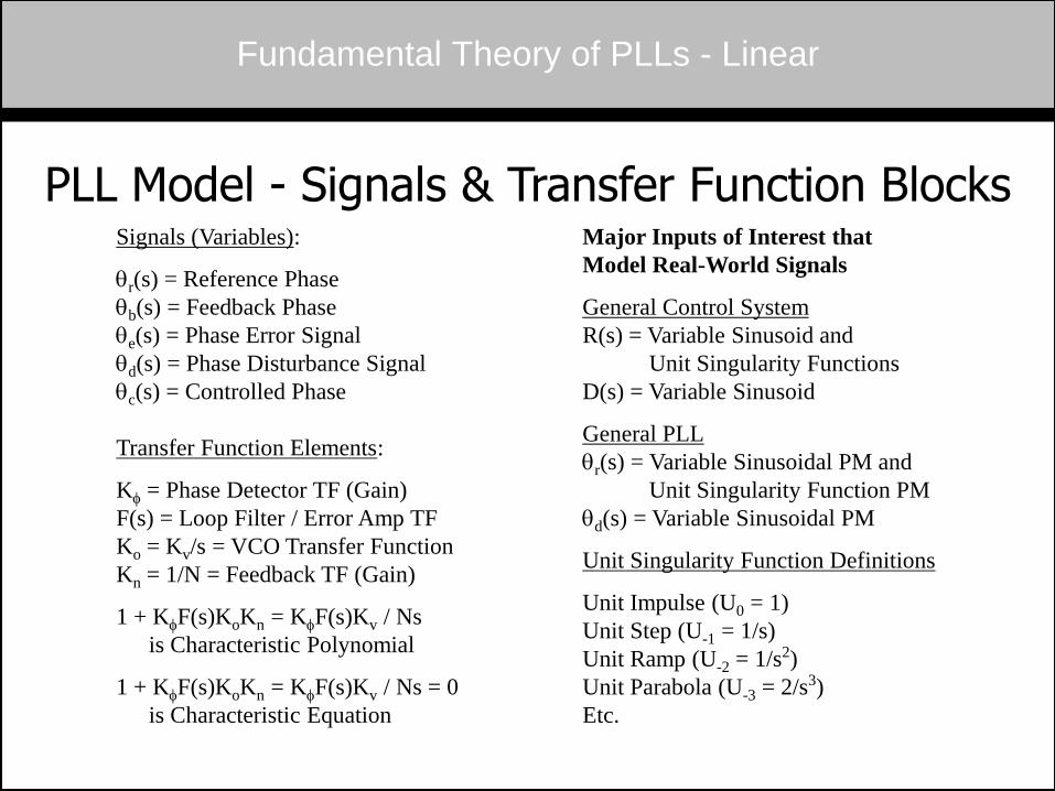
PLL Model - Signals & Transfer Function Blocks
Fundamental Theory of PLLs - Linear
Signals (Variables):
qr(s) = Reference Phase
qb(s) = Feedback Phase
qe(s) = Phase Error Signal
qd(s) = Phase Disturbance Signal
qc(s) = Controlled Phase
Transfer Function Elements:
Kf = Phase Detector TF (Gain)
F(s) = Loop Filter / Error Amp TF
Ko = Kv/s = VCO Transfer Function
Kn = 1/N = Feedback TF (Gain)
1 + KfF(s)KoKn = KfF(s)Kv / Ns
is Characteristic Polynomial
1 + KfF(s)KoKn = KfF(s)Kv / Ns = 0
is Characteristic Equation
Major Inputs of Interest that
Model Real-World Signals
General Control System
R(s) = Variable Sinusoid and
Unit Singularity Functions
D(s) = Variable Sinusoid
General PLL
qr(s) = Variable Sinusoidal PM and
Unit Singularity Function PM
qd(s) = Variable Sinusoidal PM
Unit Singularity Function Definitions
Unit Impulse (U0 = 1)
Unit Step (U-1 = 1/s)
Unit Ramp (U-2 = 1/s2)
Unit Parabola (U-3 = 2/s3)
Etc.
1TG(s)H(s)for
N,K
1
H(s)
1
N
1
s
KF(s)K1
s
KF(s)K
KF(s)KK1
F(s)KK
)s(H)s(G1
G(s)
(s)θ
(s)θ
R(s)
C(s)T
:C)-(ROutput
FunctionsTransfer Pass-Low Loop-Closed
N
1
s
KF(s)KKF(s)KK)s(H)s(G
(s)θ
(s)θ
R(s)
B(s)T
:B)-(RFeedback -Reference
FunctionTransfer (s)]θ[at Loop-Open
l-o
nv
v
no
o
r
cc-r
vno
r
bl-o
b
f
f
f
f
ff
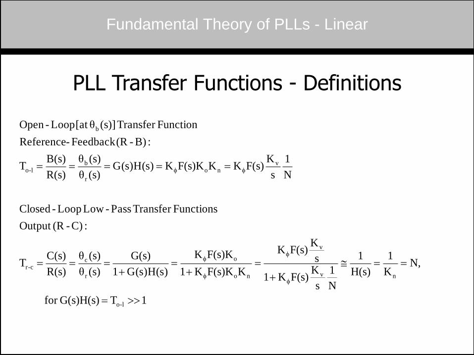
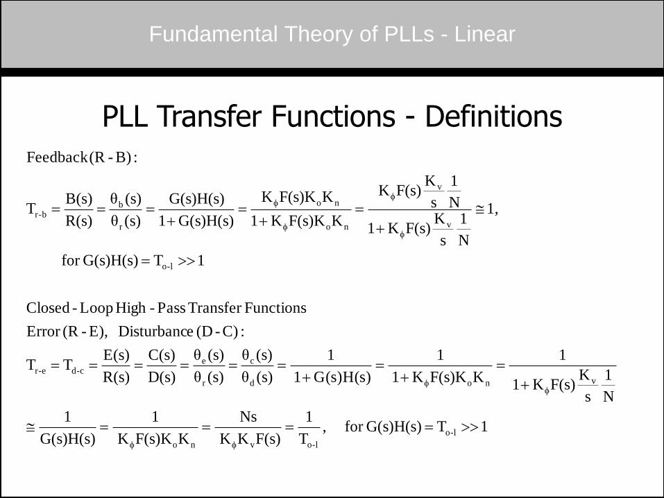
PLL Transfer Functions - Definitions
Fundamental Theory of PLLs - Linear
1TG(s)H(s)for ,T
1
F(s)KK
Ns
KF(s)KK
1
G(s)H(s)
1
N
1
s
KF(s)K1
1
KF(s)KK1
1
)s(H)s(G1
1
(s)θ
(s)θ
(s)θ
(s)θ
D(s)
C(s)
R(s)
E(s)TT
:C)-(D eDisturbanc E),-(RError
FunctionsTransfer Pass-High Loop-Closed
1TG(s)H(s)for
1,
N
1
s
KF(s)K1
N
1
s
KF(s)K
KF(s)KK1
KF(s)KK
G(s)H(s)1
G(s)H(s)
(s)θ
(s)θ
R(s)
B(s)T
:B)-(RFeedback
l-o
l-ovno
vnod
c
r
ec-de-r
l-o
v
v
no
no
r
bb-r
ff
ff
f
f
f
f
Fundamental Theory of PLLs - Linear
PLL Transfer Functions - Definitions
PLL Transfer Functions - Definitions
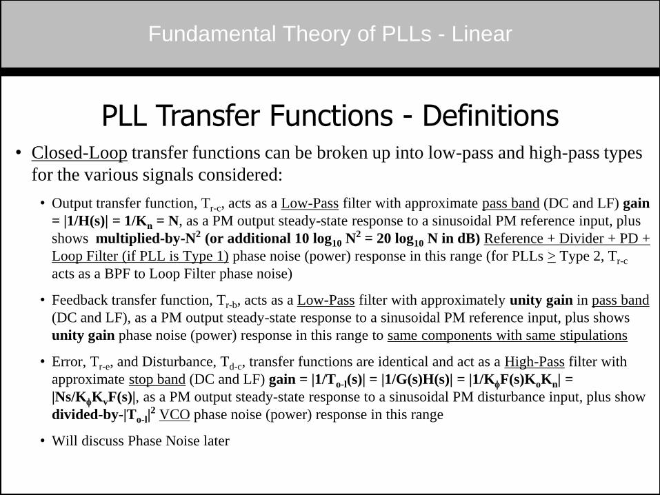
• Closed-Loop transfer functions can be broken up into low-pass and high-pass types
for the various signals considered:
• Output transfer function, Tr-c, acts as a Low-Pass filter with approximate pass band (DC and LF) gain
= |1/H(s)| = 1/Kn = N, as a PM output steady-state response to a sinusoidal PM reference input, plus
shows multiplied-by-N2 (or additional 10 log10 N2 = 20 log10 N in dB) Reference + Divider + PD +
Loop Filter (if PLL is Type 1) phase noise (power) response in this range (for PLLs > Type 2, Tr-c
acts as a BPF to Loop Filter phase noise)
• Feedback transfer function, Tr-b, acts as a Low-Pass filter with approximately unity gain in pass band
(DC and LF), as a PM output steady-state response to a sinusoidal PM reference input, plus shows
unity gain phase noise (power) response in this range to same components with same stipulations
• Error, Tr-e, and Disturbance, Td-c, transfer functions are identical and act as a High-Pass filter with
approximate stop band (DC and LF) gain = |1/To-l(s)| = |1/G(s)H(s)| = |1/KfF(s)KoKn| =
|Ns/KfKvF(s)|, as a PM output steady-state response to a sinusoidal PM disturbance input, plus show
divided-by-|To-l|2 VCO phase noise (power) response in this range
• Will discuss Phase Noise later
Fundamental Theory of PLLs - Linear
Fundamental Theory of PLLs - Linear
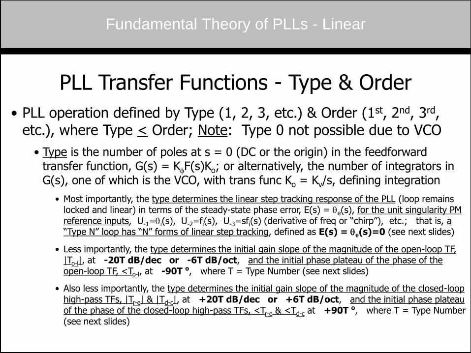
PLL Transfer Functions - Type & Order
• PLL operation defined by Type (1, 2, 3, etc.) & Order (1st, 2nd, 3rd, etc.), where Type < Order; Note: Type 0 not possible due to VCO
• Type is the number of poles at s = 0 (DC or the origin) in the feedforward transfer function, G(s) = KfF(s)Ko; or alternatively, the number of integrators in G(s), one of which is the VCO, with trans func Ko = Kv/s, defining integration
• Most importantly, the type determines the linear step tracking response of the PLL (loop remains locked and linear) in terms of the steady-state phase error, E(s) = qe(s), for the unit singularity PM reference inputs, U-1=qi(s), U-2=fi(s), U-3=sfi(s) (derivative of freq or “chirp”), etc.; that is, a “Type N” loop has “N” forms of linear step tracking, defined as E(s) = qe(s)=0 (see next slides)
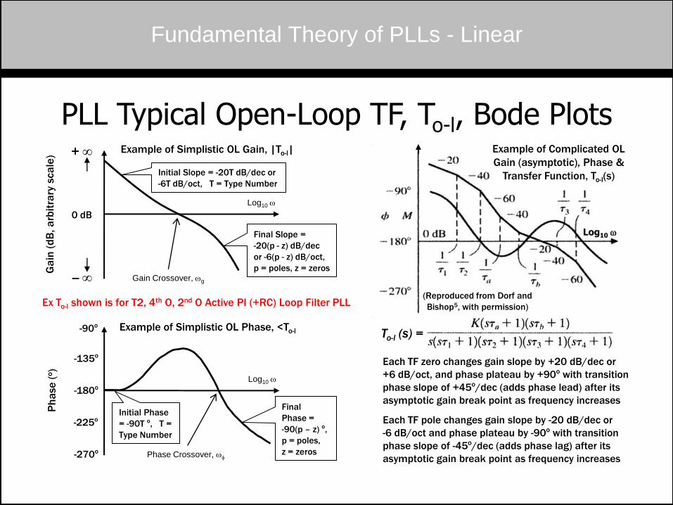
• Less importantly, the type determines the initial gain slope of the magnitude of the open-loop TF, |To-l|, at -20T dB/dec or -6T dB/oct, and the initial phase plateau of the phase of the open-loop TF, <To-l, at -90T o, where T = Type Number (see next slides)
• Also less importantly, the type determines the initial gain slope of the magnitude of the closed-loop high-pass TFs, |Tr-e| & |Td-c|, at +20T dB/dec or +6T dB/oct, and the initial phase plateau of the phase of the closed-loop high-pass TFs, <Tr-e & <Td-c at +90T o, where T = Type Number (see next slides)
Fundamental Theory of PLLs - Linear
PLL Transfer Functions - Type & Order
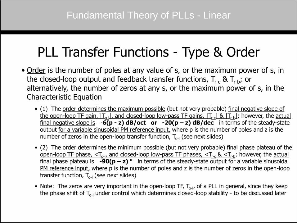
• Order is the number of poles at any value of s, or the maximum power of s, in the closed-loop output and feedback transfer functions, Tr-c & Tr-b; or alternatively, the number of zeros at any s, or the maximum power of s, in the Characteristic Equation
• (1) The order determines the maximum possible (but not very probable) final negative slope of the open-loop TF gain, |To-l|, and closed-loop low-pass TF gains, |Tr-c| & |Tr-b|; however, the actual final negative slope is -6(p - z) dB/oct or -20(p – z) dB/dec in terms of the steady-state output for a variable sinusoidal PM reference input, where p is the number of poles and z is the number of zeros in the open-loop transfer function, To-l (see next slides)
• (2) The order determines the minimum possible (but not very probable) final phase plateau of the open-loop TF phase, <To-l, and closed-loop low-pass TF phases, <Tr-c & <Tr-b; however, the actual final phase plateau is -90(p – z) o in terms of the steady-state output for a variable sinusoidal PM reference input, where p is the number of poles and z is the number of zeros in the open-loop transfer function, To-l (see next slides)
• Note: The zeros are very important in the open-loop TF, To-l, of a PLL in general, since they keep the phase shift of To-l under control which determines closed-loop stability - to be discussed later
Fundamental Theory of PLLs - Linear
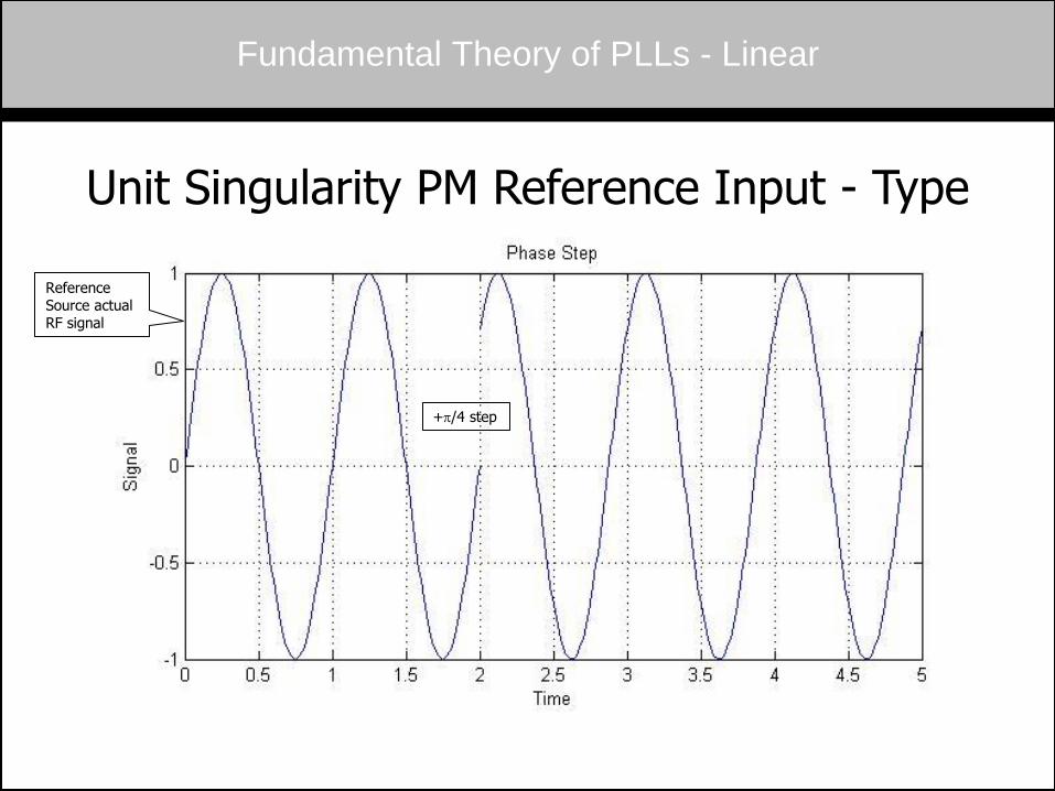
Unit Singularity PM Reference Input - Type
Reference Source actual RF signal
+p/4 step
Fundamental Theory of PLLs - Linear
Unit Singularity PM Reference Input - Type
Reference Source actual RF signal
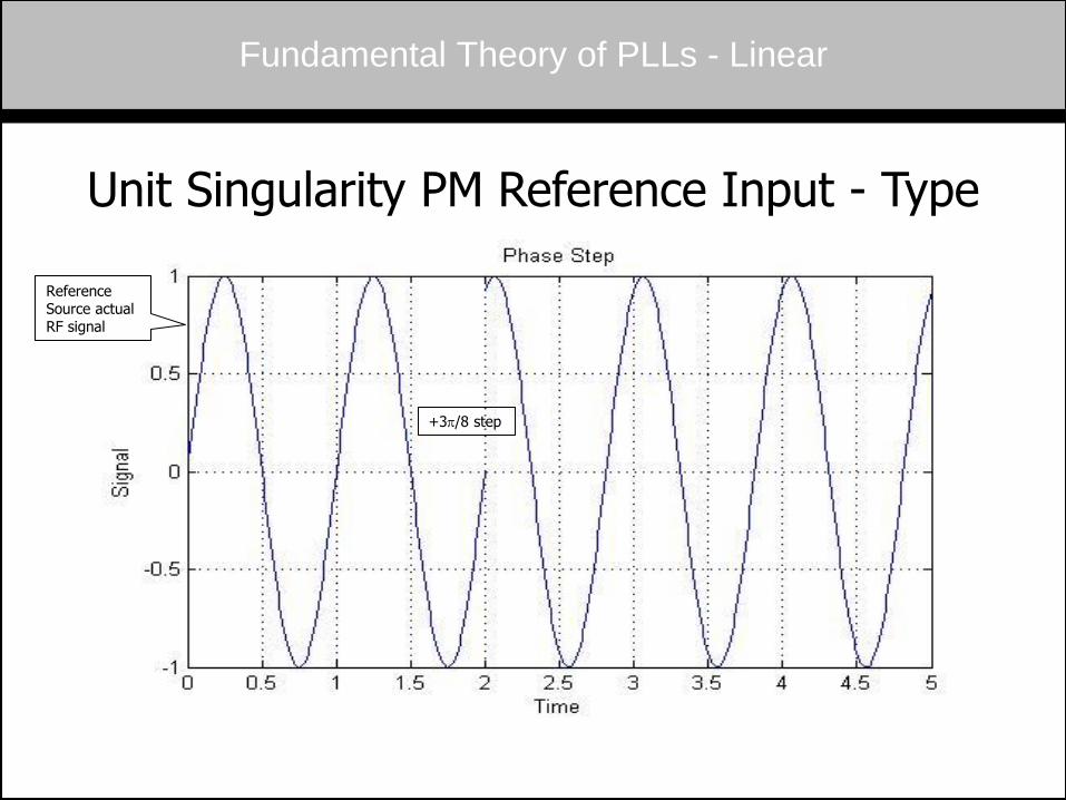
+3p/8 step
Fundamental Theory of PLLs - Linear
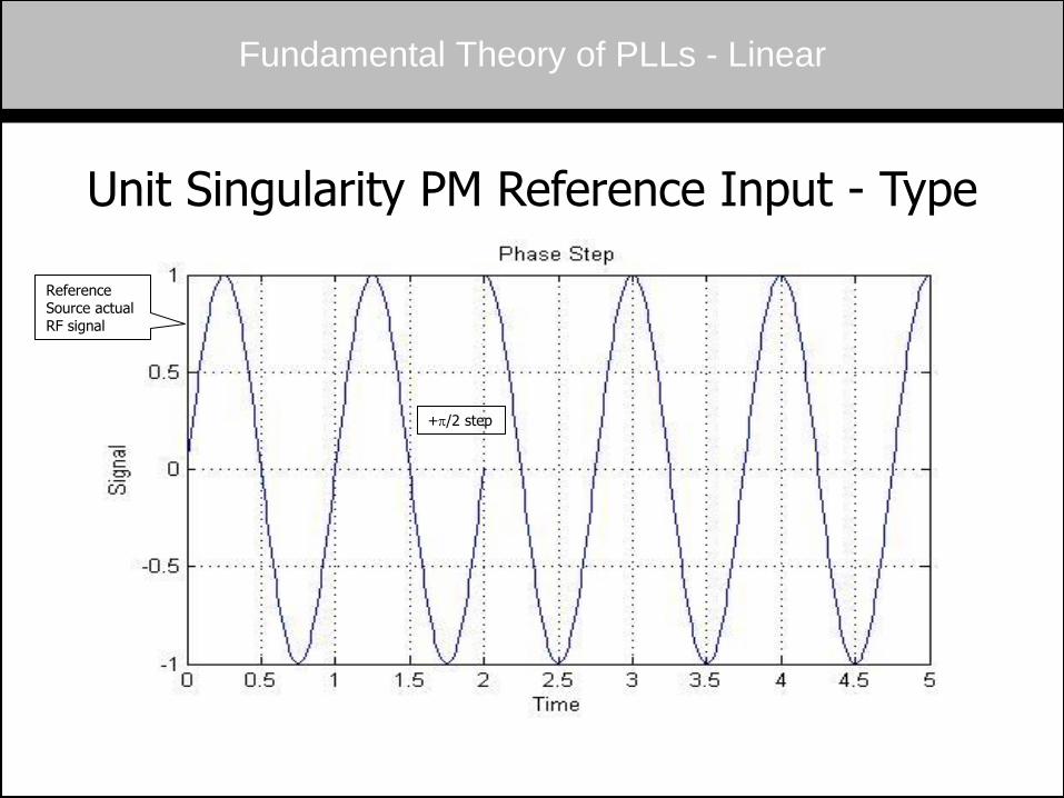
Unit Singularity PM Reference Input - Type
Reference Source actual RF signal
+p/2 step
Fundamental Theory of PLLs - Linear
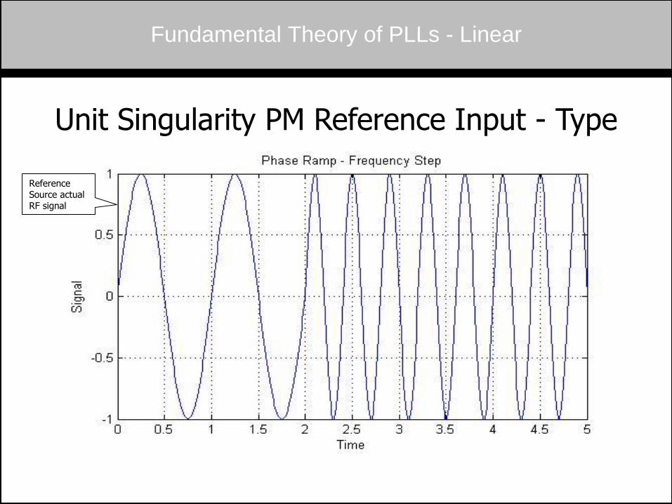
Unit Singularity PM Reference Input - Type
Reference Source actual RF signal
Fundamental Theory of PLLs - Linear
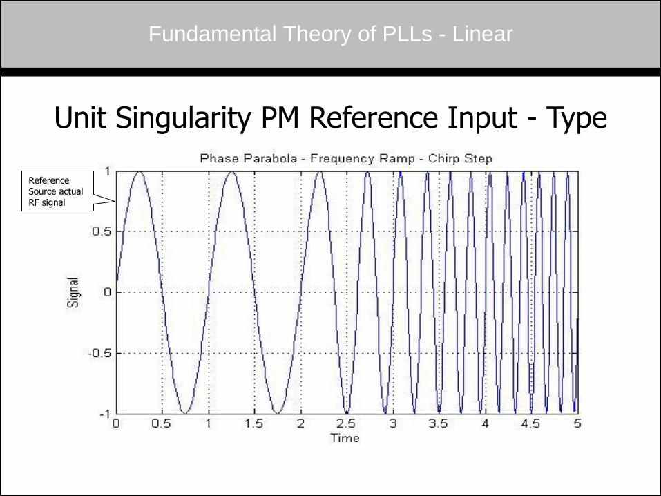
Unit Singularity PM Reference Input - Type
Reference Source actual RF signal
Fundamental Theory of PLLs - Linear
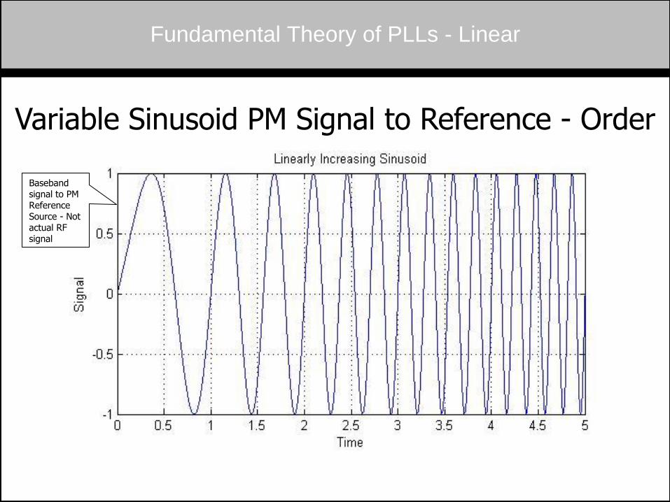
Variable Sinusoid PM Signal to Reference - Order
Baseband signal to PM Reference Source - Not actual RF signal
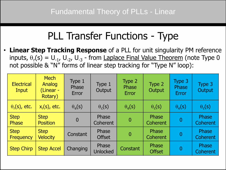
PLL Transfer Functions - Type
• Linear Step Tracking Response of a PLL for unit singularity PM reference inputs, qr(s) = U-1, U-2, U-3 - from Laplace Final Value Theorem (note Type 0 not possible & “N” forms of linear step tracking for “Type N” loop):
Electrical Input
Mech Analog
(Linear - Rotary)
Type 1 Phase Error
Type 1 Output
Type 2 Phase Error
Type 2 Output
Type 3 Phase Error
Type 3 Output
qr(s), etc. xr(s), etc. qe(s) qc(s) qe(s) qc(s) qe(s) qc(s)
Step Phase
Step Position
0 Phase
Coherent 0
Phase Coherent
0 Phase
Coherent
Step Frequency
Step Velocity
Constant Phase Offset
0 Phase
Coherent 0
Phase Coherent
Step Chirp Step Accel Changing Phase
Unlocked Constant
Phase Offset
0 Phase
Coherent
Fundamental Theory of PLLs - Linear
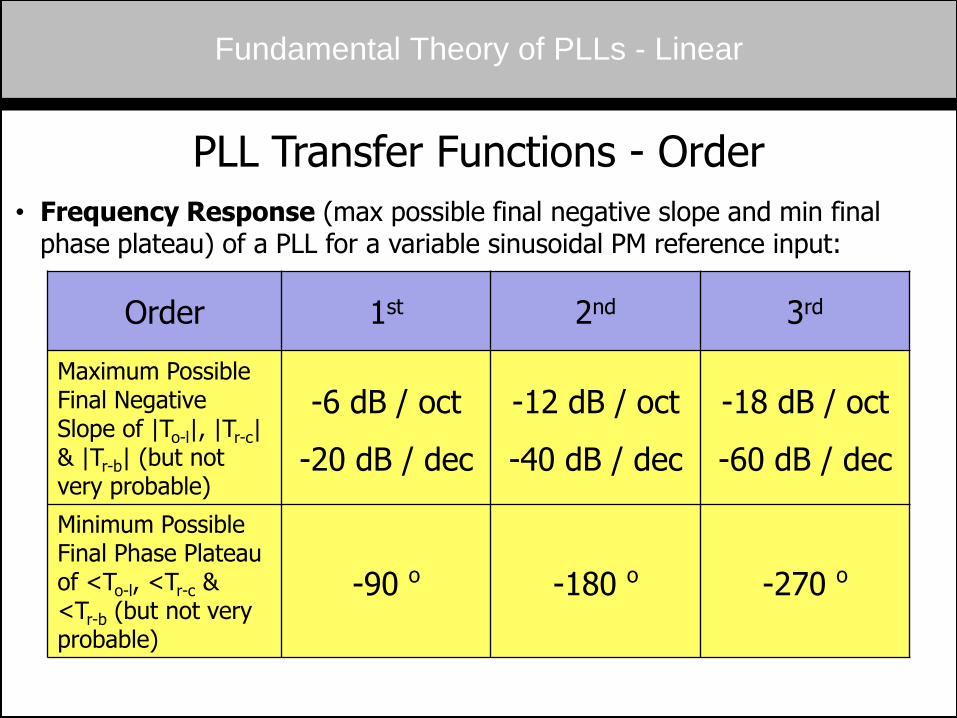
PLL Transfer Functions - Order
• Frequency Response (max possible final negative slope and min final phase plateau) of a PLL for a variable sinusoidal PM reference input:
Order 1st 2nd 3rd
Maximum Possible Final Negative Slope of |To-l|, |Tr-c| & |Tr-b| (but not very probable)
-6 dB / oct
-20 dB / dec
-12 dB / oct
-40 dB / dec
-18 dB / oct
-60 dB / dec
Minimum Possible Final Phase Plateau of <To-l, <Tr-c & <Tr-b (but not very probable)
-90 o -180 o -270 o
Fundamental Theory of PLLs - Linear
Fundamental Theory of PLLs - Linear
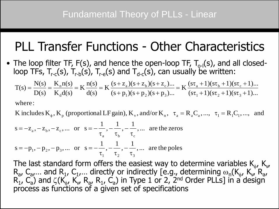
PLL Transfer Functions - Other Characteristics
• TFs are also categorized in phase as being “Lead”, “Lag”, or combinations (i.e., “Lead-Lag”). A given TF has a “Lead” phase response if its phase change becomes more positive as frequency increases, and a “Lag” phase response if its phase change becomes more negative as frequency increases
• The most common definition of output closed-loop TF (Tr-c) “Bandwidth” is the open-loop (To-l) gain crossover frequency, wg, but there are others (e.g., wn for 2nd order systems, w-3dB and wpeak for all systems)
• Undamped natural oscillation (resonant) frequency, wn, half-power bandwidth, w-3dB, and peak frequency, wpeak, are typically not the same as open-loop gain crossover frequency, wg, but are usually very close, relative to the loop BW
• As stated, the open-loop TF (To-l) gain crossover frequency, wg, and the output closed-loop TF (Tr-c) “-3 dB” frequency, w-3dB, are generally not the same, although there is a particular case where they are the same - Type 1, 1st Order PLL (only Type 1 possible for 1st Order PLL - Type 0 not possible due to VCO integrating action)
Fundamental Theory of PLLs - Linear
PLL Transfer Functions - Other Characteristics
• The loop filter TF, F(s), and hence the open-loop TF, To-l(s), and all closed-loop TFs, Tr-c(s), Tr-b(s), Tr-e(s) and Td-c(s), can usually be written:
The last standard form offers the easiest way to determine variables Kf, Kv, Ra, Ca,… and R1, C1,… directly or indirectly [e.g., determining wn(Kf, Kv, Ra, R1, Ca) and z(Kf, Kv, Ra, R1, Ca) in Type 1 or 2, 2nd Order PLLs] in a design process as functions of a given set of specifications
poles theare ... ,1
,1
,1
sor ... ,p ,p ,ps
zeros theare ... ,1
,1
,1
sor ... ,z ,z ,zs
and ..., ,CR ..., ,CR ,Kand/or ,K gain), LF nal(proportio K ,K includesK
:where
1)...1)(s1)(s(s
1)...1)(s1)(s(sK
)...p)(sp)(sp(s
)...z)(sz)(sz(sK
d(s)
n(s)K
d(s)K
n(s)K
D(s)
N(s)T(s)
321
321
cba
cba
111aaanvp
321
cba
321
cba
d
n
f
Fundamental Theory of PLLs - Linear
PLL Typical Open-Loop TF, To-l, Bode Plots
Log10 w
Log10 w
Phase Crossover, wf
Each TF zero changes gain slope by +20 dB/dec or
+6 dB/oct, and phase plateau by +90o with transition
phase slope of +45o/dec (adds phase lead) after its
asymptotic gain break point as frequency increases
Each TF pole changes gain slope by -20 dB/dec or
-6 dB/oct and phase plateau by -90o with transition
phase slope of -45o/dec (adds phase lag) after its
asymptotic gain break point as frequency increases
Gain Crossover, wg
Ph
ase
(o)
To-l (s) =
Log10 w
-90o
-180o
-135o
-270o
-225o
Example of Complicated OL
Gain (asymptotic), Phase &
Transfer Function, To-l(s)
Example of Simplistic OL Gain, |To-l|
Example of Simplistic OL Phase, <To-l
(Reproduced from Dorf and
Bishop5, with permission)
Ga
in (
dB
, a
rbit
rary
sca
le)
0 dB
--
+
Initial Slope = -20T dB/dec or
-6T dB/oct, T = Type Number
Initial Phase
= -90T o, T =
Type Number
Final Slope =
-20(p - z) dB/dec
or -6(p - z) dB/oct,
p = poles, z = zeros
Final
Phase =
-90(p – z) o,
p = poles,
z = zeros
Ex To-l shown is for T2, 4th O, 2nd O Active PI (+RC) Loop Filter PLL
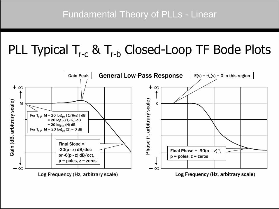
PLL Typical Tr-c & Tr-b Closed-Loop TF Bode Plots
Fundamental Theory of PLLs - Linear
Ph
ase
(o, a
rbit
rary
sca
le)
Ga
in (
dB
, a
rbit
rary
sca
le)
Log Frequency (Hz, arbitrary scale) Log Frequency (Hz, arbitrary scale)
General Low-Pass Response
--
0
+
--
M
+
E(s) = qe(s) = 0 in this region Gain Peak
For Tr-c: M = 20 log10 |1/H(s)| dB
= 20 log10 (1/Kn) dB
= 20 log10 (N) dB
For Tr-b: M = 20 log10 (1) = 0 dB
Final Slope =
-20(p - z) dB/dec
or -6(p - z) dB/oct,
p = poles, z = zeros
Final Phase = -90(p – z) o,
p = poles, z = zeros
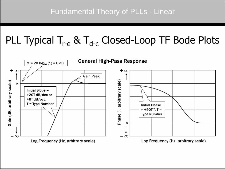
PLL Typical Tr-e & Td-c Closed-Loop TF Bode Plots
Fundamental Theory of PLLs - Linear G
ain
(d
B, a
rbit
rary
sca
le)
Ph
ase
(o, a
rbit
rary
sca
le)
Log Frequency (Hz, arbitrary scale) Log Frequency (Hz, arbitrary scale)
General High-Pass Response
--
0
+
--
M
+
Gain Peak
M = 20 log10 (1) = 0 dB
Initial Slope =
+20T dB/dec or
+6T dB/oct,
T = Type Number Initial Phase
= +90T o, T =
Type Number
Fundamental Theory of PLLs - Linear
PLL Stability
• Stability is probably the most important consideration in PLL (or general control system) design (a system is basically useless if it is not stable) and TFs are designed as a function of stability considerations as well as other performance specs
• The common denominator for addressing stability of a PLL (or general control system) is the open-loop transfer function, To-l
• There are 5 predominant methods for investigating stability as a system parameter (usually |To-l|) is varied :
• Root Locus Plot (uses To-l embedded in CE) - widely used for PLLs and servos
• Bode Plot (uses To-l directly) - widely used for PLLs and servos
• Nichols Diagram (uses To-l directly) - not used (but recommended) for PLLs, but widely used for servos
• Nyquist Diagram (uses To-l directly) - not widely used for PLLs or servos
• Routh-Hurwitz Array (uses To-l embedded in CE) - actual usage unknown
• Out of the first 4 methods, the most comprehensive is the Root Locus Plot, since it shows system stability for all values of open-loop gain variable, K = |To-l|, in one plot
• The Routh-Hurwitz Array is not discussed, since it depends on advanced math involving matrix calculations, and does not seem to be applied to PLLs in the industry
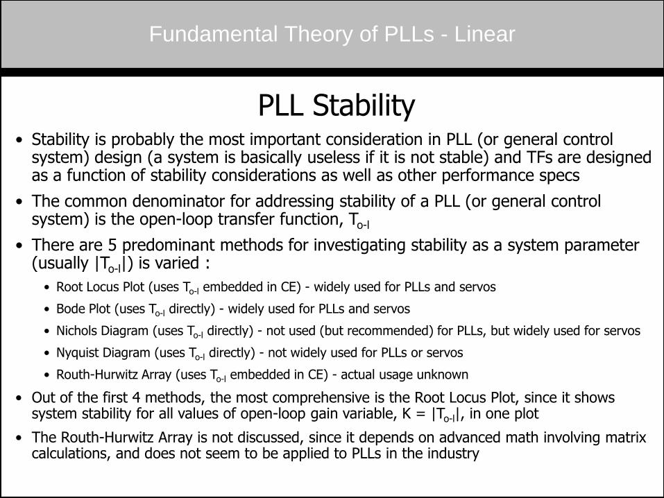
PLL Stability - Stable & Unstable Cases - Synth
Typical PLL Synthesizer Output on Spectrum Analyzer
PLL Stable - Ideal Profile Stability Margins Moderately Degraded
Fundamental Theory of PLLs - Linear
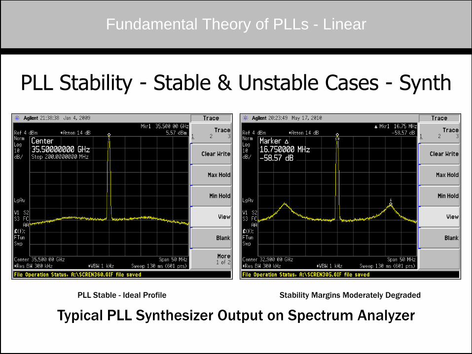
PLL Stability - Stable & Unstable Cases - Synth
Typical PLL Synthesizer Output on Spectrum Analyzer
Stability Margins Moderately Degraded - Wider Span Stability Margins Severely Degraded
Fundamental Theory of PLLs - Linear
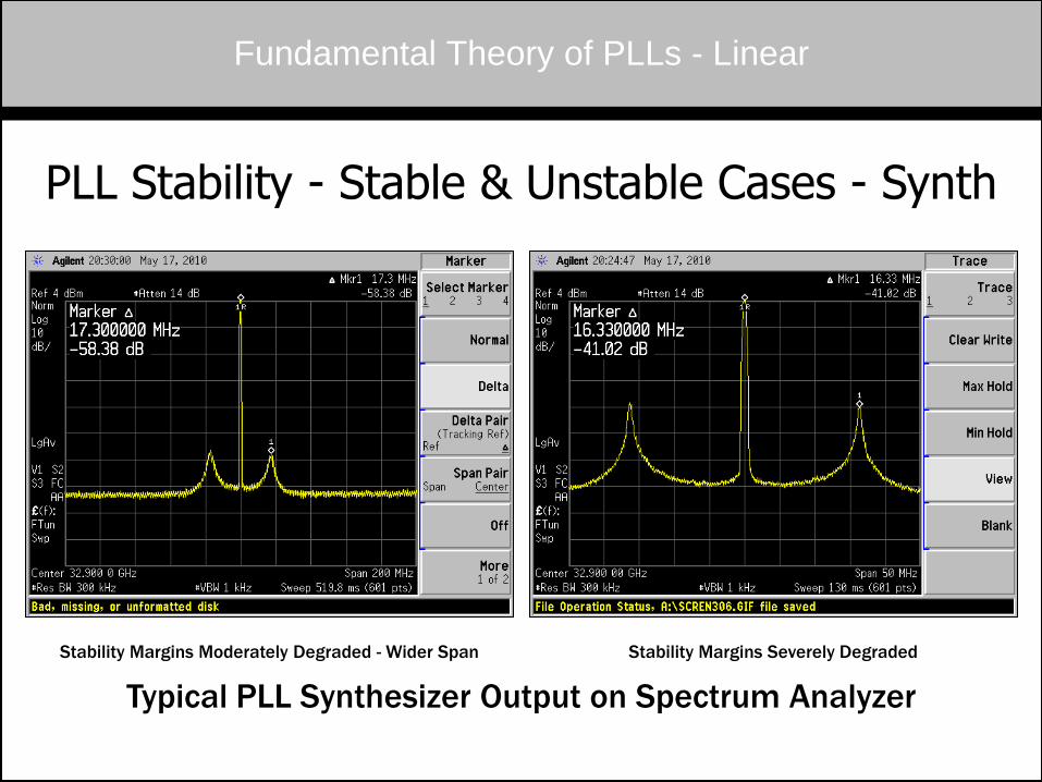
PLL Stability - Stable & Unstable Cases - Synth
Typical PLL Synthesizer Output on Spectrum Analyzer
Stability Margins Severely Degraded - Wider Span PLL Unstable - Discrete Mode(s) Oscillation
Fundamental Theory of PLLs - Linear
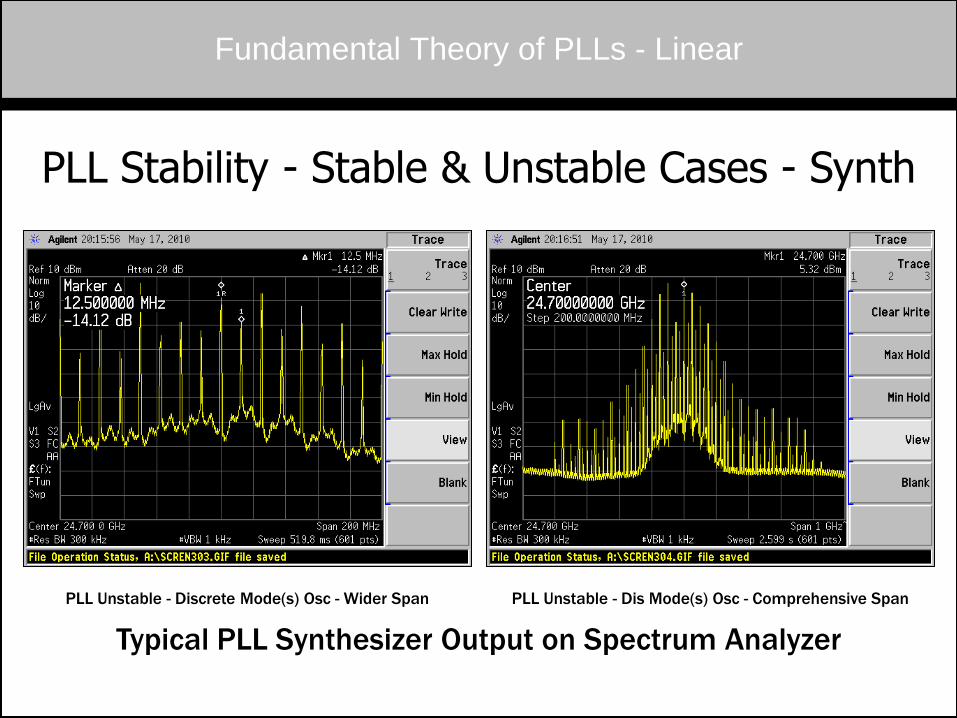
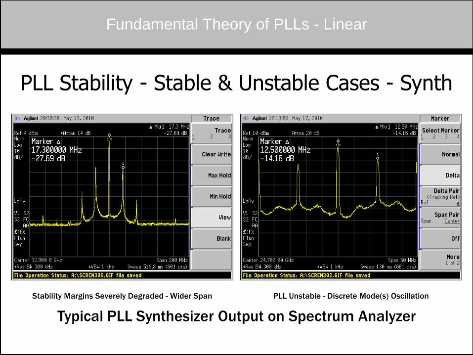
PLL Stability - Stable & Unstable Cases - Synth
Typical PLL Synthesizer Output on Spectrum Analyzer
PLL Unstable - Discrete Mode(s) Osc - Wider Span PLL Unstable - Dis Mode(s) Osc - Comprehensive Span
Fundamental Theory of PLLs - Linear
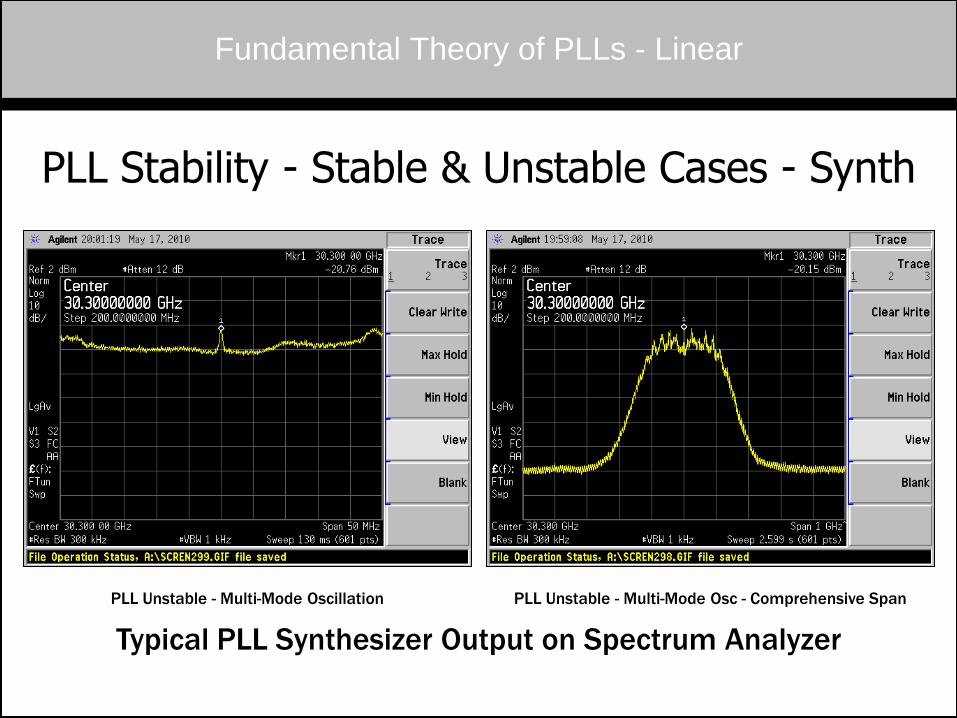
PLL Stability - Stable & Unstable Cases - Synth
Typical PLL Synthesizer Output on Spectrum Analyzer
PLL Unstable - Multi-Mode Oscillation PLL Unstable - Multi-Mode Osc - Comprehensive Span
Fundamental Theory of PLLs - Linear
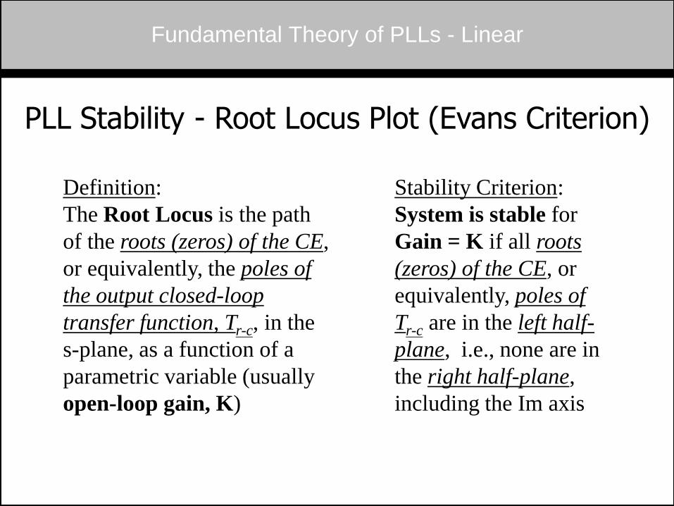
PLL Stability - Root Locus Plot (Evans Criterion)
Definition:
The Root Locus is the path
of the roots (zeros) of the CE,
or equivalently, the poles of
the output closed-loop
transfer function, Tr-c, in the
s-plane, as a function of a
parametric variable (usually
open-loop gain, K)
Fundamental Theory of PLLs - Linear
Stability Criterion:
System is stable for
Gain = K if all roots
(zeros) of the CE, or
equivalently, poles of
Tr-c are in the left half-
plane, i.e., none are in
the right half-plane,
including the Im axis
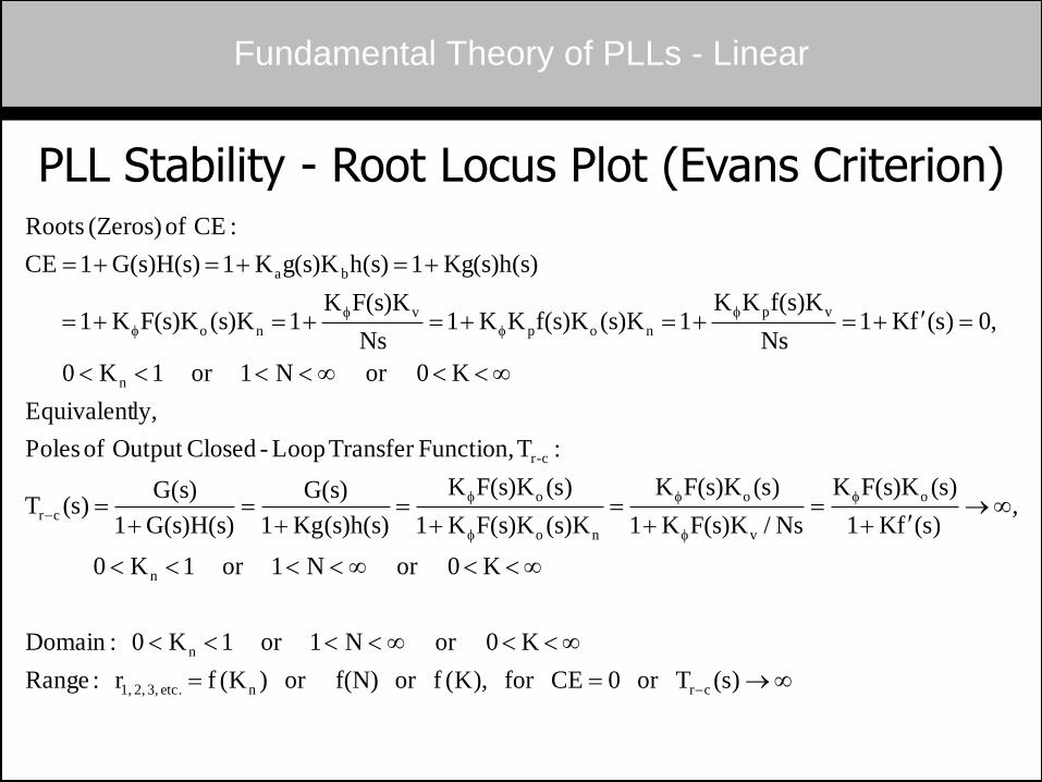
PLL Stability - Root Locus Plot (Evans Criterion)
f
f
f
f
f
f
f
f
f
)s(Tor 0CEfor ,)K(for f(N)or )K(fr :Range
K 0or N1or 1K0 :Domain
K 0or N1or 1K0
,)s(fK1
)s(F(s)KK
Ns/F(s)KK1
)s(F(s)KK
(s)KF(s)KK1
)s(F(s)KK
(s)h(s)Kg1
G(s)
G(s)H(s)1
G(s))s(T
: T Function,Transfer Loop-ClosedOutput of Poles
,lyEquivalent
K 0or N1or 1K0
,0)s(fK1Ns
f(s)KKK1(s)Kf(s)KKK1
Ns
F(s)KK1(s)KF(s)KK1
Kg(s)h(s)1h(s)g(s)KK1G(s)H(s)1CE
:CE of (Zeros) Roots
crnetc. 3, 2, 1,
n
n
o
v
o
no
o
cr
c-r
n
vp
nop
v
no
ba
Fundamental Theory of PLLs - Linear
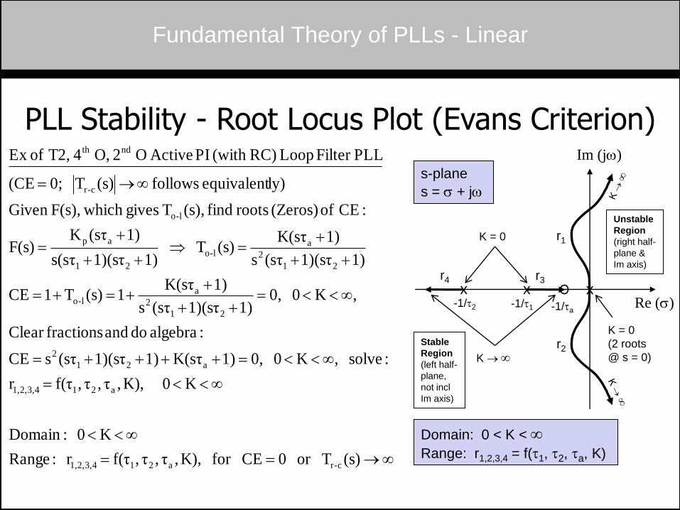
PLL Stability - Root Locus Plot (Evans Criterion)
(s)Tor 0CEfor K),,τ,τ,f(τr :Range
K 0 :Domain
K 0 K),,τ,τ,f(τr
:solve , K 0 0,1)K(sτ1)1)(sτ(sτsCE
:algebra do and fractionsClear
, K 0 0,1)1)(sτ(sτs
1)K(sτ1(s)T1CE
1)1)(sτ(sτs
1)K(sτ(s)T
1)1)(sτs(sτ
1)(sτKF(s)
:CE of (Zeros) roots find (s),T gives which F(s),Given
ly)equivalent follows (s)T 0; (CE
PLLFilter Loop RC)(with PI Active O 2 O, 4 T2, ofEx
c-ra211,2,3,4
a211,2,3,4
a21
2
21
2
al-o
21
2
al-o
21
ap
l-o
c-r
ndth
Re (s)
Im (jw)
K = 0
s-plane
s = s + jw
Domain: 0 < K < Range: r1,2,3,4 = f(1, 2, a, K)
Fundamental Theory of PLLs - Linear
r1
r2
r3
K
Unstable
Region
(right half-
plane &
Im axis)
Stable
Region
(left half-
plane,
not incl
Im axis)
x x x r4
K = 0
(2 roots
@ s = 0)
-1/a
-1/1 -1/2
PLL Stability - Root Locus Plot (Evans Criterion)
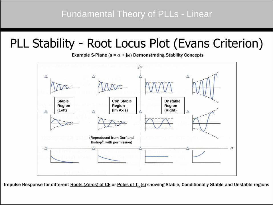
Fundamental Theory of PLLs - Linear
Unstable
Region
(Right)
Stable
Region
(Left)
Impulse Response for different Roots (Zeros) of CE or Poles of Tr-c(s) showing Stable, Conditionally Stable and Unstable regions
Example S-Plane (s = s + jw) Demonstrating Stability Concepts
Con Stable
Region
(Im Axis)
(Reproduced from Dorf and
Bishop5, with permission)
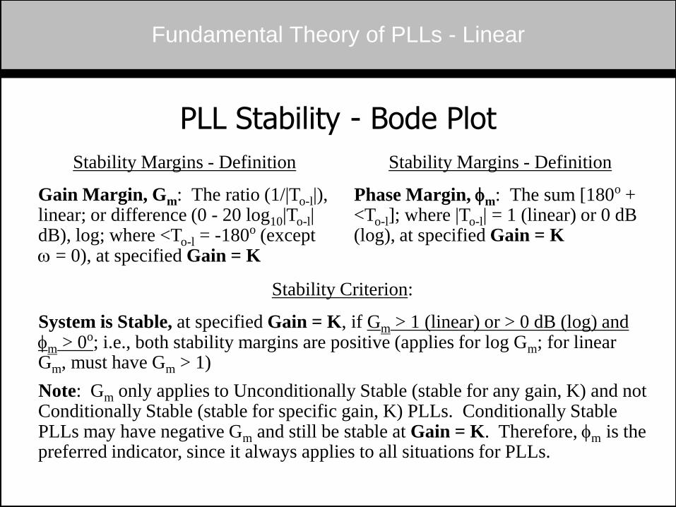
PLL Stability - Bode Plot
Fundamental Theory of PLLs - Linear
Stability Margins - Definition
Gain Margin, Gm: The ratio (1/|To-l|), linear; or difference (0 - 20 log10|To-l| dB), log; where <To-l = -180o (except w = 0), at specified Gain = K
Stability Criterion:
System is Stable, at specified Gain = K, if Gm > 1 (linear) or > 0 dB (log) and fm > 0o; i.e., both stability margins are positive (applies for log Gm; for linear Gm, must have Gm > 1)
Note: Gm only applies to Unconditionally Stable (stable for any gain, K) and not Conditionally Stable (stable for specific gain, K) PLLs. Conditionally Stable PLLs may have negative Gm and still be stable at Gain = K. Therefore, fm is the preferred indicator, since it always applies to all situations for PLLs.
Stability Margins - Definition
Phase Margin, fm: The sum [180o + <To-l]; where |To-l| = 1 (linear) or 0 dB (log), at specified Gain = K
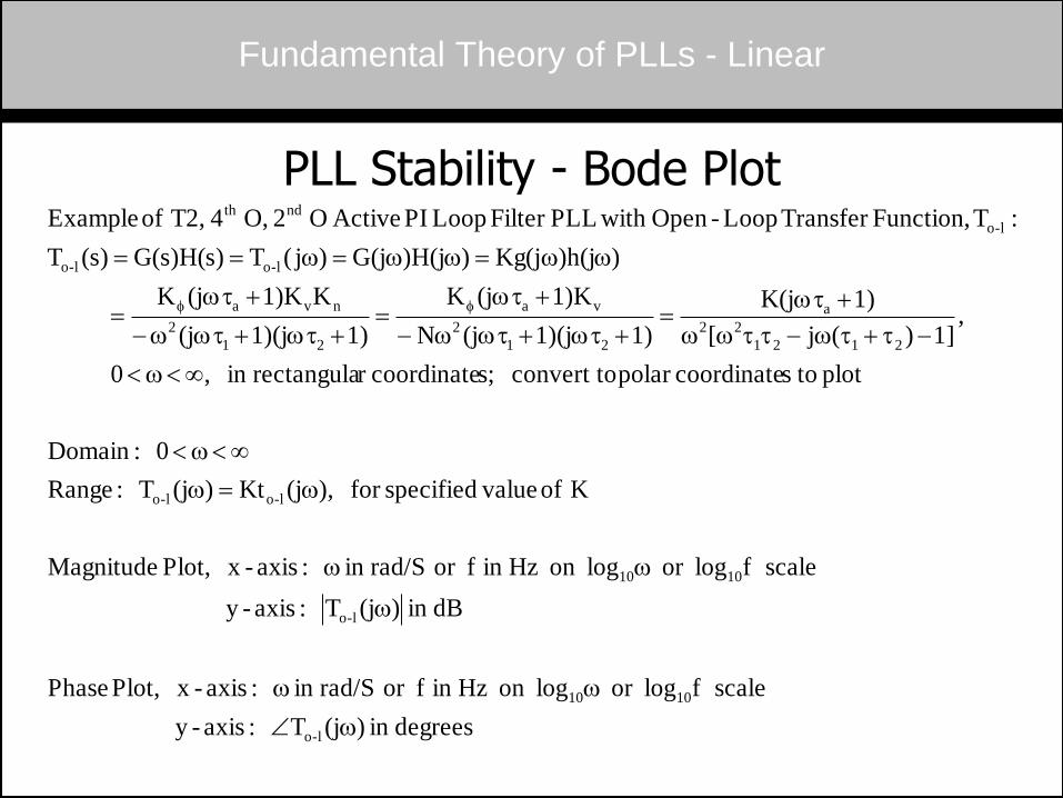
PLL Stability - Bode Plot
Fundamental Theory of PLLs - Linear
degreesin )(jT :axis-y
scale flogor logon Hzin for rad/Sin :axis- xPlot, Phase
dBin )(jT :axis-y
scale flogor logon Hzin for rad/Sin :axis- xPlot, Magnitude
K of valuespecifiedfor ),(jKt)(jT :Range
0 :Domain
plot toscoordinatepolar convert to s;coordinater rectangulain , 0
,1])(j[
1)K(j
1)1)(j(jN
1)K(jK
1)1)(j(j
K1)K(jK
))h(jKg(j))H(jG(j)j(T)s)H(sG()s(T
:T Function,Transfer Loop-Open with PLLFilter Loop PI Active O 2 O, 4 T2, of Example
l-o
1010
l-o
1010
l-ol-o
2121
22
a
21
2
va
21
2
nva
l-ol-o
l-o
ndth
w
ww
w
ww
ww
w
w
www
w
www
w
www
w
wwwww
ff
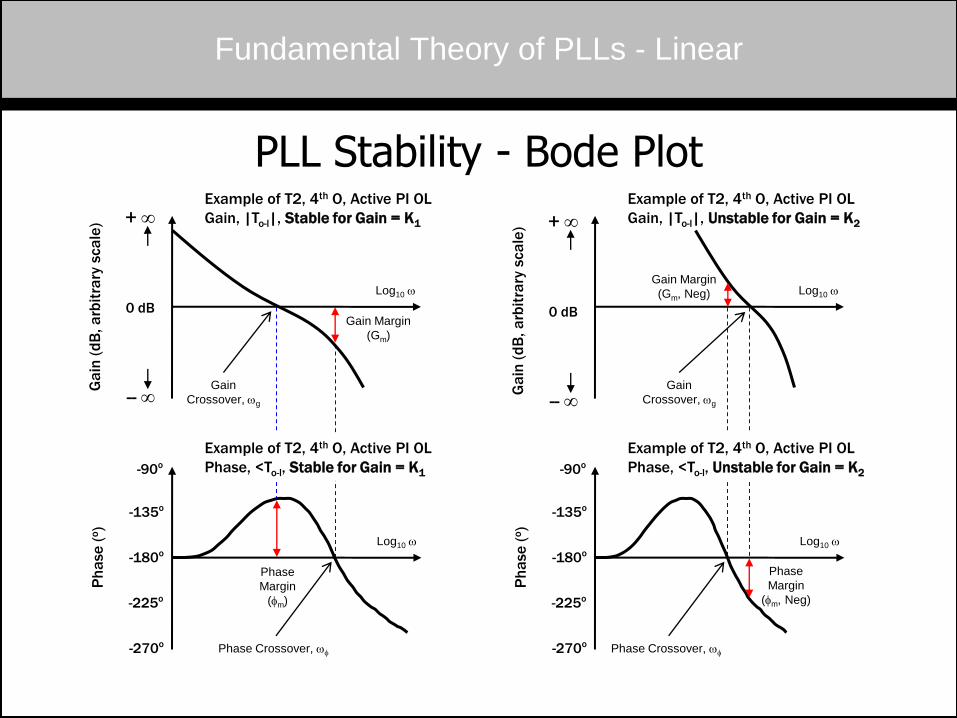
PLL Stability - Bode Plot
Fundamental Theory of PLLs - Linear
Log10 w
Log10 w
Phase Crossover, wf
Gain
Crossover, wg
Gain Margin
(Gm)
Phase
Margin
(fm)
Ga
in (
dB
, a
rbit
rary
sca
le)
Ph
ase
(o)
-90o
-180o
-135o
-270o
-225o
0 dB
Example of T2, 4th O, Active PI OL
Gain, |To-l|, Stable for Gain = K1
Example of T2, 4th O, Active PI OL
Phase, <To-l, Stable for Gain = K1
Log10 w
Log10 w
Ph
ase
(o)
-90o
-180o
-135o
-270o
-225o
Example of T2, 4th O, Active PI OL
Gain, |To-l|, Unstable for Gain = K2
Example of T2, 4th O, Active PI OL
Phase, <To-l, Unstable for Gain = K2
--
+
Gain Margin
(Gm, Neg)
Phase
Margin
(fm, Neg)
Phase Crossover, wf
Gain
Crossover, wg
Ga
in (
dB
, a
rbit
rary
sca
le)
0 dB
--
+
Fundamental Theory of PLLs - Linear
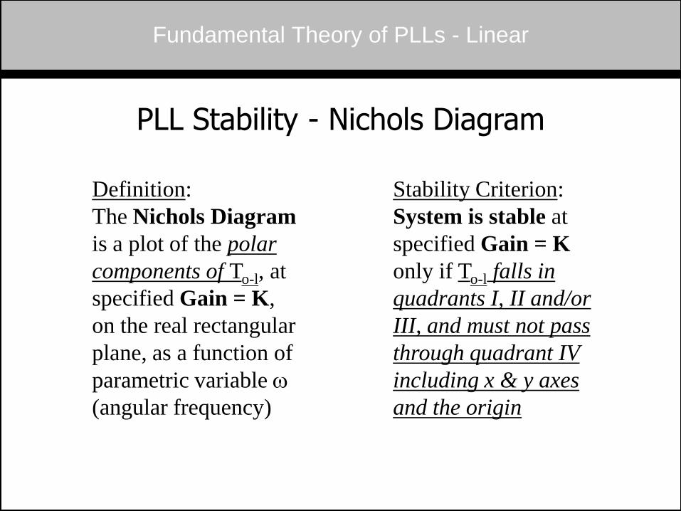
PLL Stability - Nichols Diagram
Definition:
The Nichols Diagram
is a plot of the polar
components of To-l, at
specified Gain = K,
on the real rectangular
plane, as a function of
parametric variable w
(angular frequency)
Stability Criterion:
System is stable at
specified Gain = K
only if To-l falls in
quadrants I, II and/or
III, and must not pass
through quadrant IV
including x & y axes
and the origin
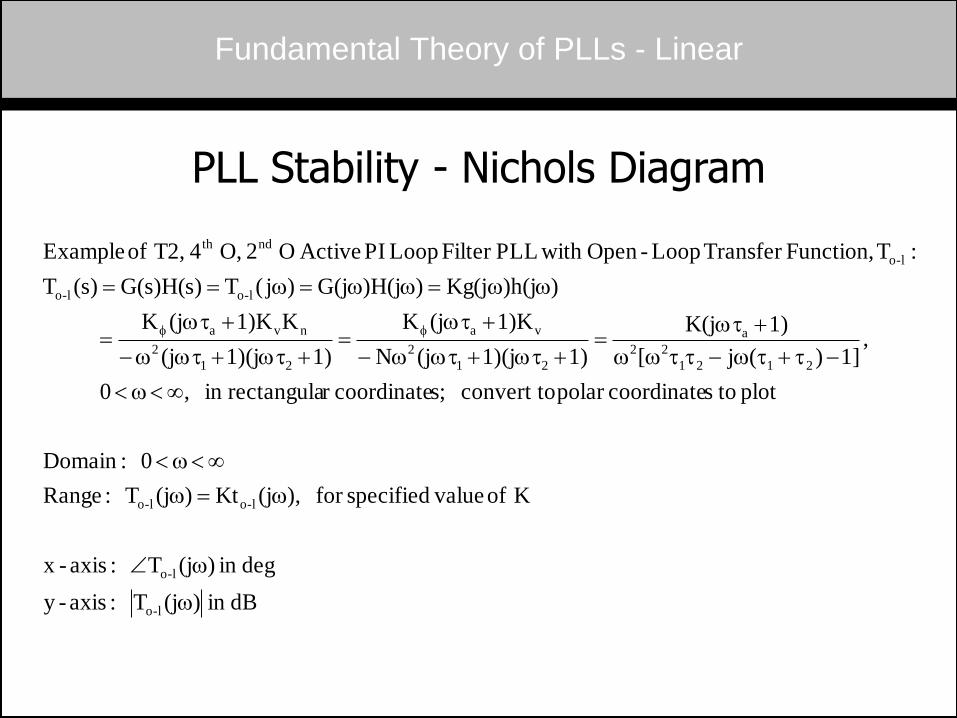
Fundamental Theory of PLLs - Linear
PLL Stability - Nichols Diagram
dBin )(jT :axis-y
degin )(jT :axis-x
K of valuespecifiedfor ),(jKt)(jT :Range
0 :Domain
plot toscoordinatepolar convert to s;coordinater rectangulain , 0
,1])(j[
1)K(j
1)1)(j(jN
1)K(jK
1)1)(j(j
K1)K(jK
))h(jKg(j))H(jG(j)j(T)s)H(sG()s(T
:T Function,Transfer Loop-Open with PLLFilter Loop PI Active O 2 O, 4 T2, of Example
l-o
l-o
l-ol-o
2121
22
a
21
2
va
21
2
nva
l-ol-o
l-o
ndth
w
w
ww
w
w
www
w
www
w
www
w
wwwww
ff
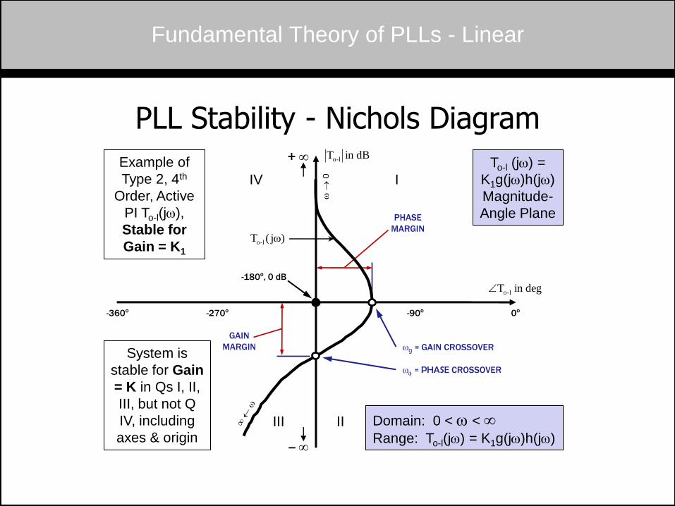
Fundamental Theory of PLLs - Linear
PLL Stability - Nichols Diagram dBin T l-o
degin T l-o
)j(T l-o w
Domain: 0 < w < Range: To-l(jw) = K1g(jw)h(jw)
To-l (jw) =
K1g(jw)h(jw)
Magnitude-
Angle Plane
Example of
Type 2, 4th
Order, Active
PI To-l(jw),
Stable for
Gain = K1
wg = GAIN CROSSOVER
wf = PHASE CROSSOVER
-180o, 0 dB
-90o -270o -360o 0o
PHASE
MARGIN
GAIN
MARGIN
w
0
III II
System is
stable for Gain
= K in Qs I, II,
III, but not Q
IV, including
axes & origin --
+
I IV
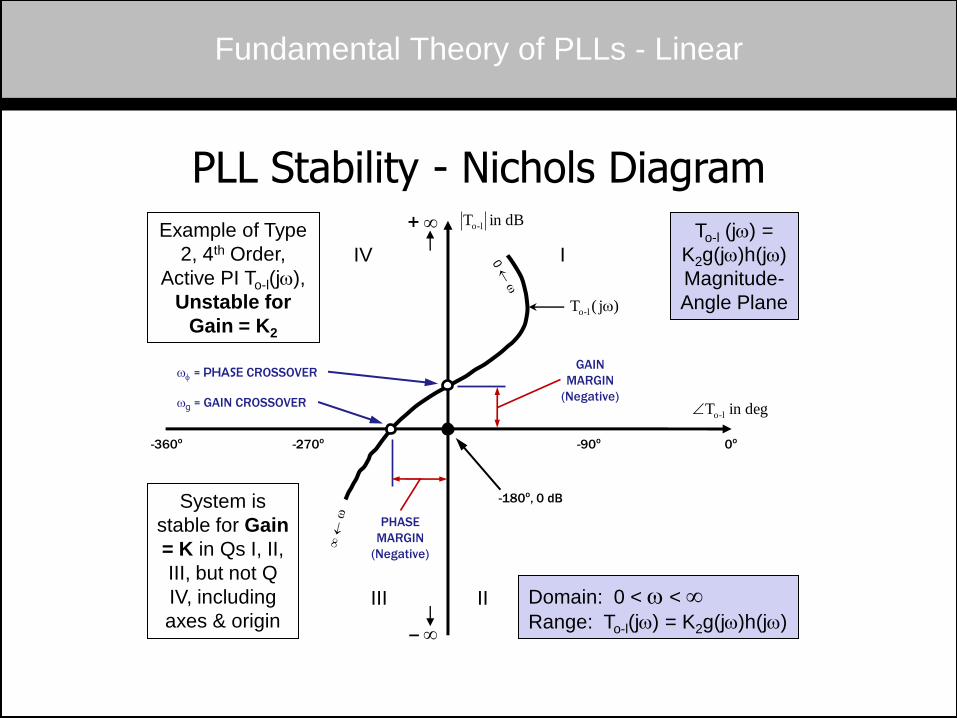
Fundamental Theory of PLLs - Linear
degin T l-o
)j(T l-o w
To-l (jw) =
K2g(jw)h(jw)
Magnitude-
Angle Plane
Example of Type
2, 4th Order,
Active PI To-l(jw),
Unstable for
Gain = K2
wg = GAIN CROSSOVER
wf = PHASE CROSSOVER
-180o, 0 dB
-90o -270o -360o 0o
PHASE
MARGIN
(Negative)
GAIN
MARGIN
(Negative)
III II
I IV
System is
stable for Gain
= K in Qs I, II,
III, but not Q
IV, including
axes & origin --
+
dBin T l-o
PLL Stability - Nichols Diagram
Domain: 0 < w < Range: To-l(jw) = K2g(jw)h(jw)
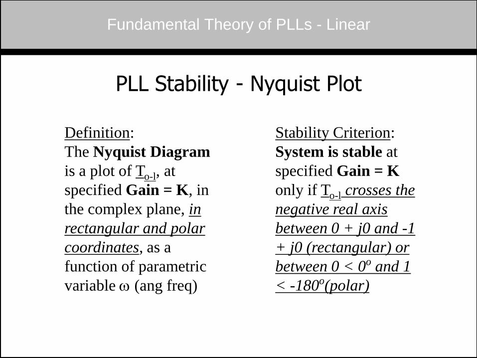
PLL Stability - Nyquist Plot
Definition:
The Nyquist Diagram
is a plot of To-l, at
specified Gain = K, in
the complex plane, in
rectangular and polar
coordinates, as a
function of parametric
variable w (ang freq)
Fundamental Theory of PLLs - Linear
Stability Criterion:
System is stable at
specified Gain = K
only if To-l crosses the
negative real axis
between 0 + j0 and -1
+ j0 (rectangular) or
between 0 < 0o and 1
< -180o(polar)
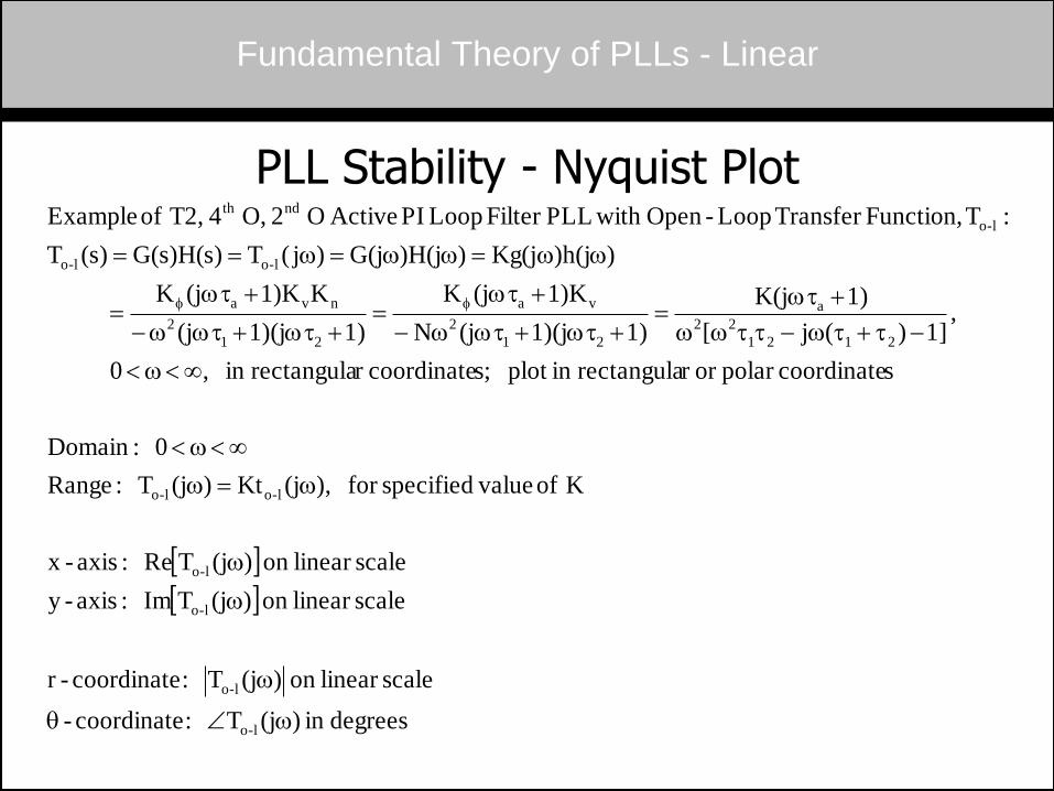
PLL Stability - Nyquist Plot
Fundamental Theory of PLLs - Linear
degreesin )(jT :coordinate-
scalelinear on )(jT :coordinate-r
scalelinear on )(jTIm :axis-y
scalelinear on )(jTRe :axis-x
K of valuespecifiedfor ),(jKt)(jT :Range
0 :Domain
scoordinatepolar or r rectangulain plot s;coordinater rectangulain , 0
,1])(j[
1)K(j
1)1)(j(jN
1)K(jK
1)1)(j(j
K1)K(jK
))h(jKg(j))H(jG(j)j(T)s)H(sG()s(T
:T Function,Transfer Loop-Open with PLLFilter Loop PI Active O 2 O, 4 T2, of Example
l-o
l-o
l-o
l-o
l-ol-o
2121
22
a
21
2
va
21
2
nva
l-ol-o
l-o
ndth
wq
w
w
w
ww
w
w
www
w
www
w
www
w
wwwww
ff
Fundamental Theory of PLLs - Linear
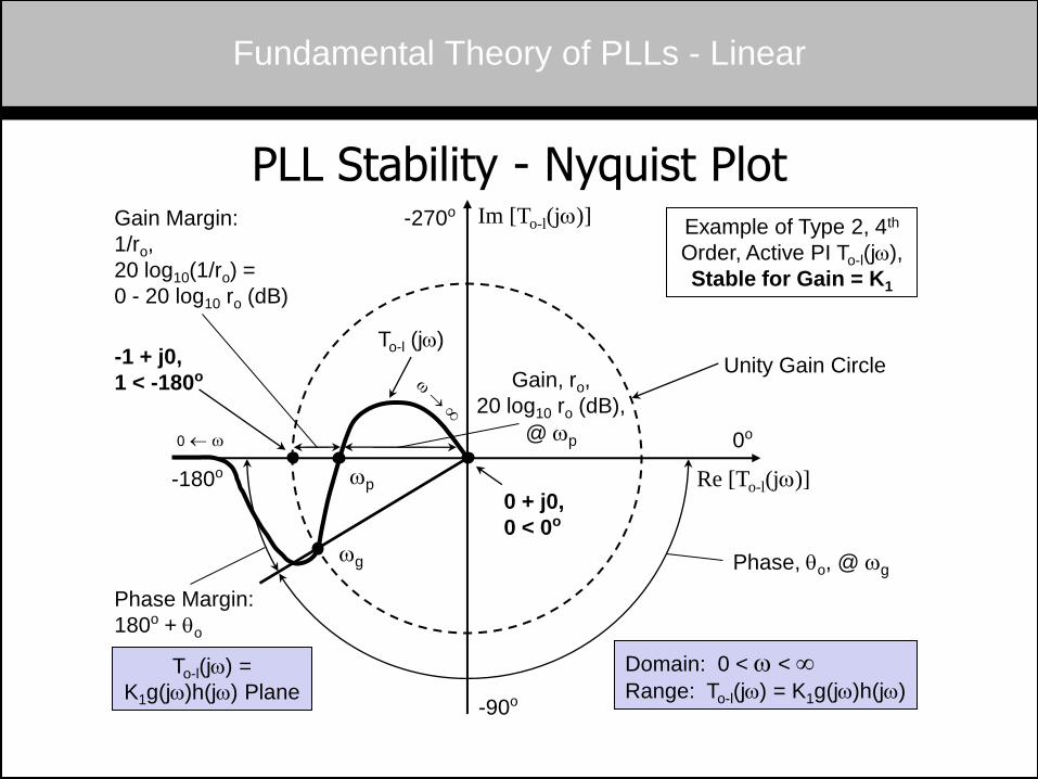
PLL Stability - Nyquist Plot
-1 + j0,
1 < -180o
wp
wg
-180o
-90o
-270o
0o
Gain Margin:
1/ro,
20 log10(1/ro) =
0 - 20 log10 ro (dB)
Phase Margin:
180o + qo
Gain, ro,
20 log10 ro (dB),
@ wp
Phase, qo, @ wg
Example of Type 2, 4th
Order, Active PI To-l(jw),
Stable for Gain = K1
Unity Gain Circle
To-l (jw)
To-l(jw) =
K1g(jw)h(jw) Plane
Domain: 0 < w < Range: To-l(jw) = K1g(jw)h(jw)
Im [To-l(jw)]
Re [To-l(jw)]
0 + j0,
0 < 0o
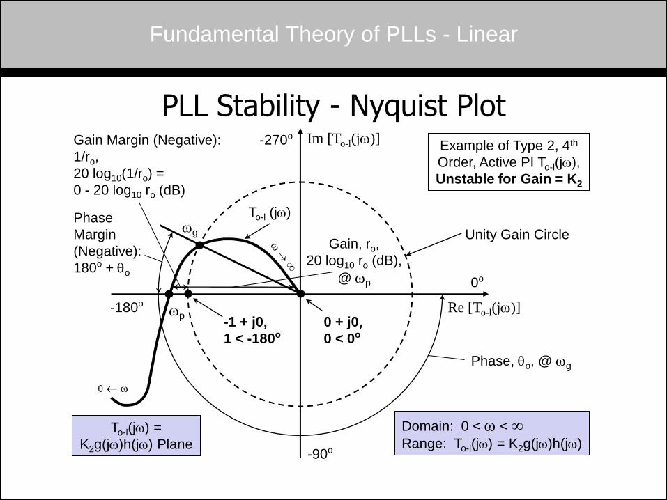
Fundamental Theory of PLLs - Linear
PLL Stability - Nyquist Plot
-1 + j0,
1 < -180o
wp
wg
-180o
-90o
-270o
0o
Gain Margin (Negative):
1/ro,
20 log10(1/ro) =
0 - 20 log10 ro (dB)
Gain, ro,
20 log10 ro (dB),
@ wp
Phase, qo, @ wg
0 + j0,
0 < 0o
Example of Type 2, 4th
Order, Active PI To-l(jw),
Unstable for Gain = K2
Unity Gain Circle
To-l (jw)
Im [To-l(jw)]
Re [To-l(jw)]
Phase
Margin
(Negative):
180o + qo
Domain: 0 < w < Range: To-l(jw) = K2g(jw)h(jw)
To-l(jw) =
K2g(jw)h(jw) Plane
PLL Stability - Routh-Hurwitz Array
(No Discussion - advanced mathematics involving matrix calculations)
Fundamental Theory of PLLs - Linear
Specific PLL Transfer Functions
• We will look at in summary: 7 Common Loop Filters/Error Amplifiers with Voltage Source PDs, giving Types 1 & 2, Orders 1, 2 & 3 Output Closed-Loop PLL TFs, Tr-c, along with Design Parameters & Stability
• We will look at in detail: Type 2, 2nd Order, 1st Order Active PI Loop Filter PLL Transfer Function with Voltage Source PD because of its universal popularity
• Current Source (A.K.A Charge Pump) PDs are universally popular also, and have some advantages, but are not considered here
• Note: For a PLL of given Type & Order, the Open- & Closed-Loop TFs, i.e., the Gain and Phase Responses, are usually not uniquely defined; the responses depend on the actual loop filter and circuit configuration
Fundamental Theory of PLLs - Linear
Specific PLL Transfer Functions - LFs/Error Amps
• Once the Kf & Ko (Kv/s) gains, along with the H(s) = Kn (1/N) gain range, have been specified for a particular design to meet a set of specifications, the Loop Filter/Error Amplifier Transfer Function, F(s), is the only variable in G(s) remaining in the Open-Loop & All Closed-Loop Transfer Functions of circuit constants to be designed
• Table (next slides) shows 7 Common LF/Error Amplifier Transfer Functions, F(s), which when substituted into Open-Loop TFs of circuit constants, compare to 3 Standard-Form Open-Loop TFs (To-l) of Physical Systems, and define 5 Standard-Form Output Closed-Loop TFs (Tr-c) of Physical Systems (other 3 closed-loop TFs, Tr-b, Tr-e, Td-c, defined same way, but not used here), along with their Final & Intermediate Design Parameters and Stability:
Fundamental Theory of PLLs - Linear
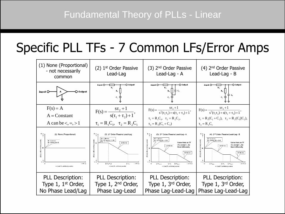
Fundamental Theory of PLLs - Linear
Specific PLL TFs - 7 Common LFs/Error Amps (1) None (Proportional)
- not necessarily common
(2) 1st Order Passive Lead-Lag
(3) 2nd Order Passive Lead-Lag - A
(4) 2nd Order Passive Lead-Lag - B
PLL Description: Type 1, 1st Order,
No Phase Lead/Lag
PLL Description: Type 1, 2nd Order, Phase Lag-Lead
PLL Description: Type 1, 3rd Order,
Phase Lag-Lead-Lag
PLL Description: Type 1, 3rd Order,
Phase Lag-Lead-Lag
122111
21
2
CR, τCRτ
,1)τ s(τ
1sτF(s)
)C(CRτ
,CR, τCRτ
,1)τs(τ)τ(τ s
1sτF(s)
2123
222111
3121
2
3
1 , , becan A
Constant A
AF(s)
123
21222111
3121
2
3
CRτ
),||C(CR), τC(CRτ
,1)τs(τ)τ(τ s
1sτF(s)
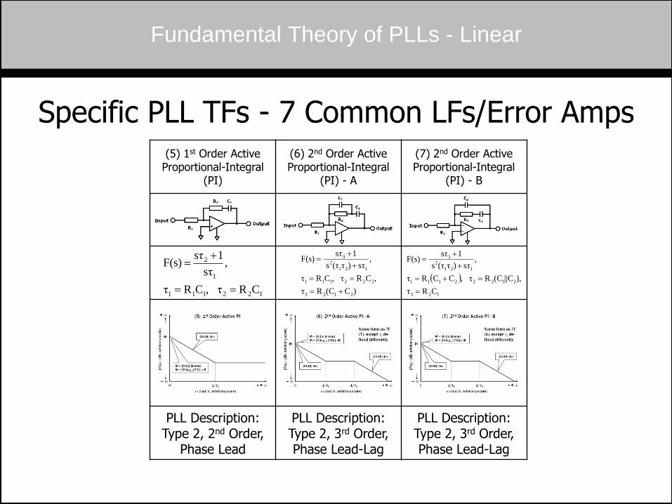
Fundamental Theory of PLLs - Linear
Specific PLL TFs - 7 Common LFs/Error Amps (5) 1st Order Active
Proportional-Integral (PI)
(6) 2nd Order Active Proportional-Integral
(PI) - A
(7) 2nd Order Active Proportional-Integral
(PI) - B
PLL Description: Type 2, 2nd Order,
Phase Lead
PLL Description: Type 2, 3rd Order, Phase Lead-Lag
PLL Description: Type 2, 3rd Order, Phase Lead-Lag
122111
1
2
CR, τCRτ
, sτ
1sτF(s)
)C(CRτ
,CR, τCRτ
,sτ)τ(τ s
1sτF(s)
2123
222111
121
2
3
123
21222111
121
2
3
CRτ
),||C(CR, τCCRτ
,sτ)τ(τ s
1sτF(s)
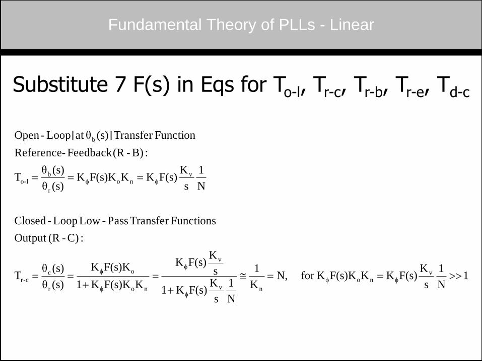
Substitute 7 F(s) in Eqs for To-l, Tr-c, Tr-b, Tr-e, Td-c
Fundamental Theory of PLLs - Linear
1N
1
s
KF(s)KKF(s)KKor f N,
K
1
N
1
s
KF(s)K1
s
KF(s)K
KF(s)KK1
F(s)KK
(s)θ
(s)θT
:C)-(ROutput
FunctionsTransfer Pass-Low Loop-Closed
N
1
s
KF(s)KKF(s)KK
(s)θ
(s)θT
:B)-(RFeedback -Reference
FunctionTransfer (s)]θ[at Loop-Open
vno
nv
v
no
o
r
cc-r
vno
r
bl-o
b
ff
f
f
f
f
ff
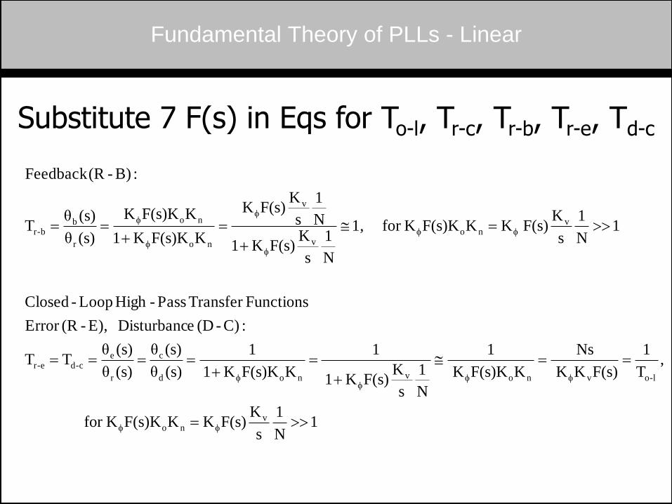
Fundamental Theory of PLLs - Linear
1N
1
s
KF(s)KKF(s)KKr of
,T
1
F(s)KK
Ns
KF(s)KK
1
N
1
s
KF(s)K1
1
KF(s)KK1
1
(s)θ
(s)θ
(s)θ
(s)θTT
:C)-(D eDisturbanc E),-(RError
FunctionsTransfer Pass-High Loop-Closed
1N
1
s
KF(s) KKF(s)KKfor 1,
N
1
s
KF(s)K1
N
1
s
KF(s)K
KF(s)KK1
KF(s)KK
(s)θ
(s)θT
:B)-(RFeedback
vno
l-ovnovnod
c
r
ec-de-r
vno
v
v
no
no
r
bb-r
ff
fff
f
ff
f
f
f
f
Substitute 7 F(s) in Eqs for To-l, Tr-c, Tr-b, Tr-e, Td-c
Fundamental Theory of PLLs - Linear
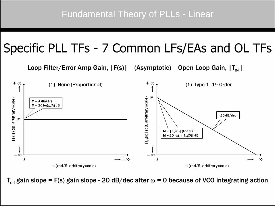
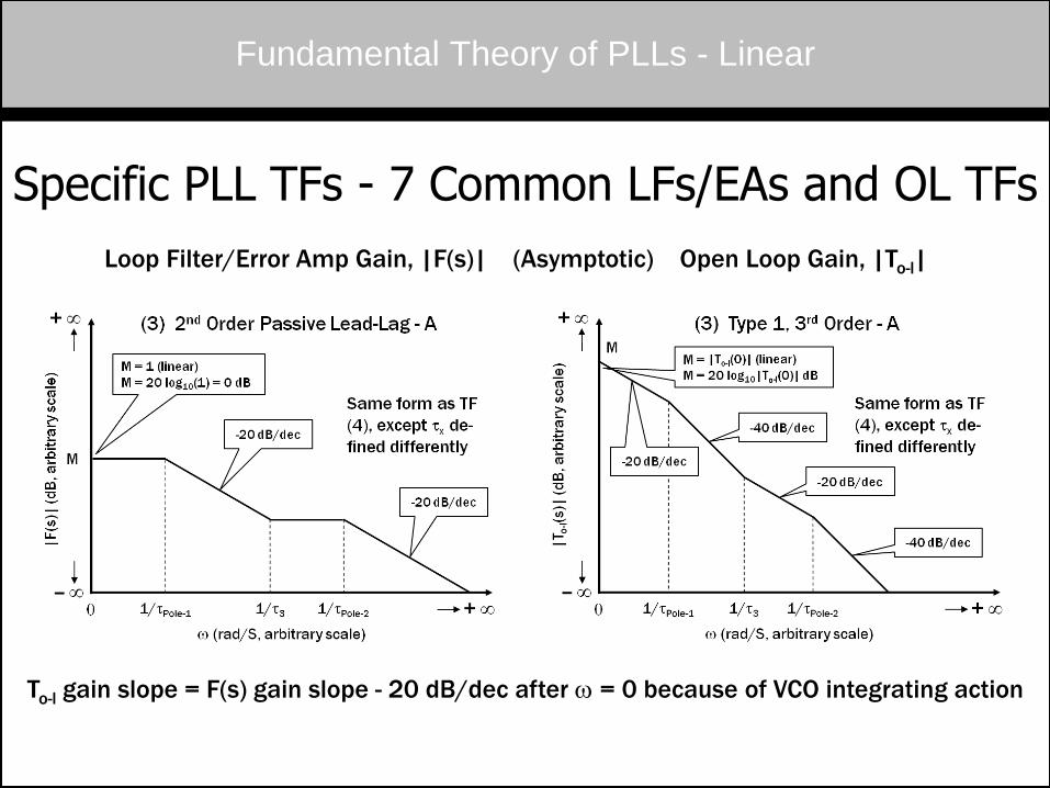
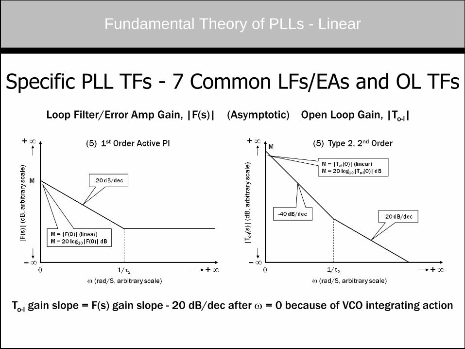
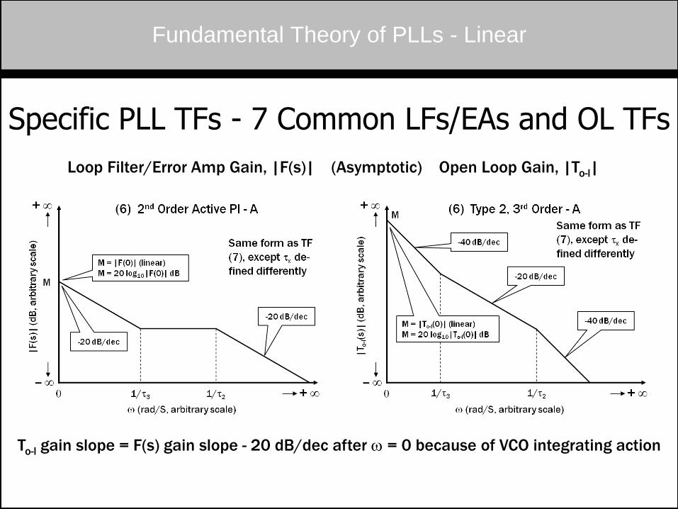
Specific PLL TFs - 7 Common LFs/EAs and OL TFs
Loop Filter/Error Amp Gain, |F(s)| (Asymptotic) Open Loop Gain, |To-l|
To-l gain slope = F(s) gain slope - 20 dB/dec after w = 0 because of VCO integrating action
Fundamental Theory of PLLs - Linear
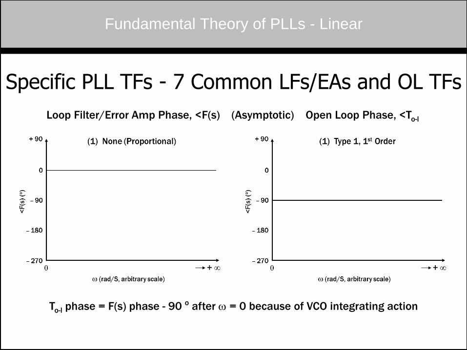
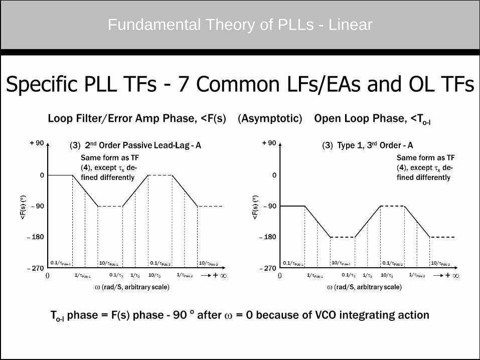
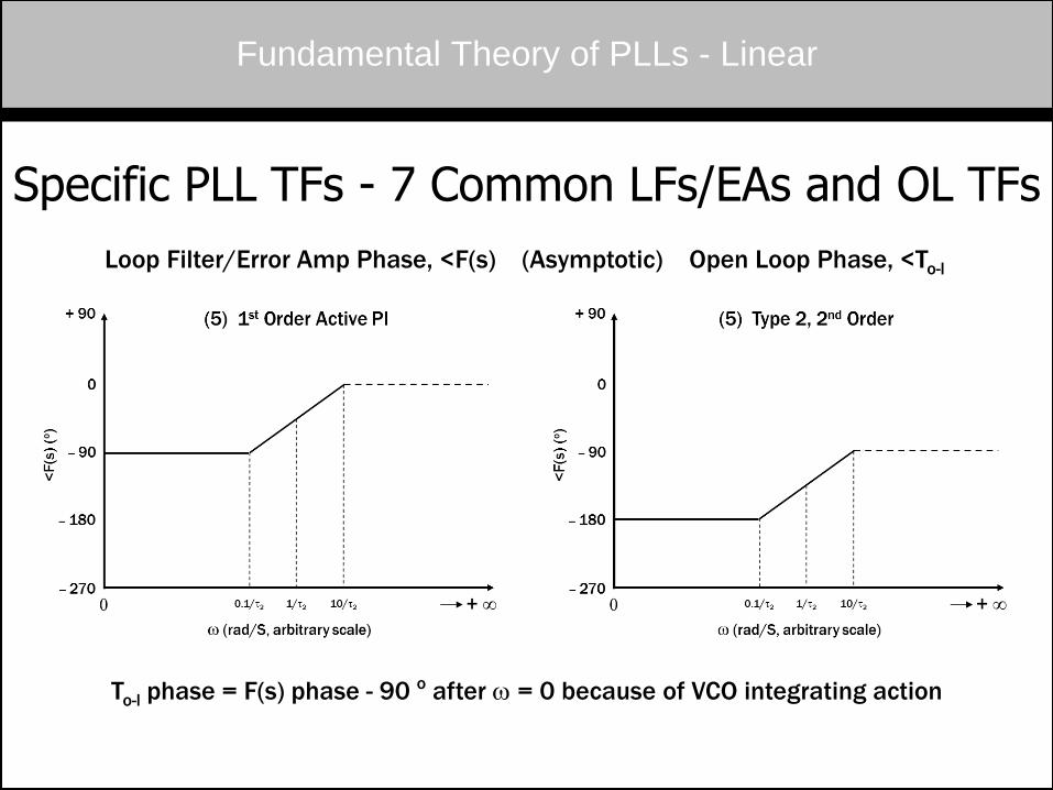
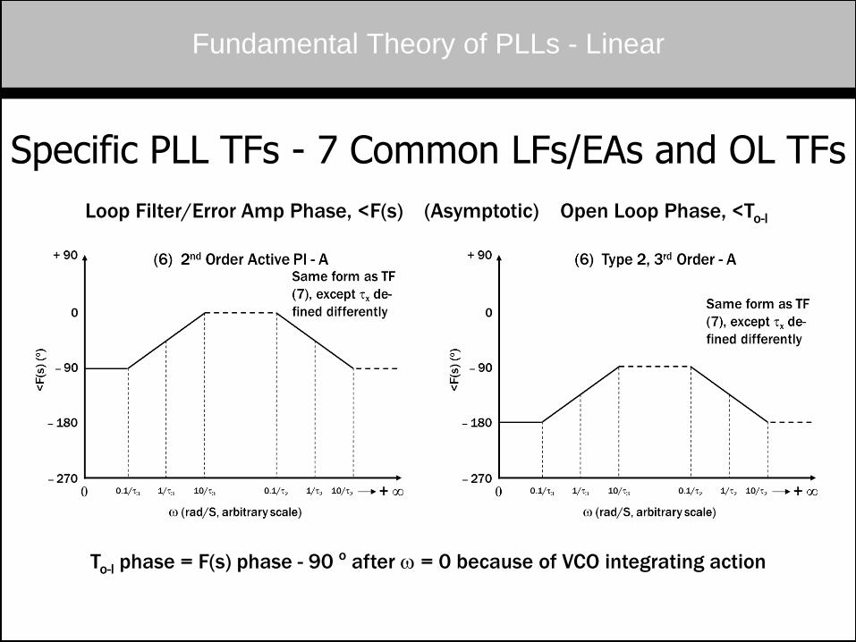
Specific PLL TFs - 7 Common LFs/EAs and OL TFs
Loop Filter/Error Amp Phase, <F(s) (Asymptotic) Open Loop Phase, <To-l
To-l phase = F(s) phase - 90 o after w = 0 because of VCO integrating action
Fundamental Theory of PLLs - Linear
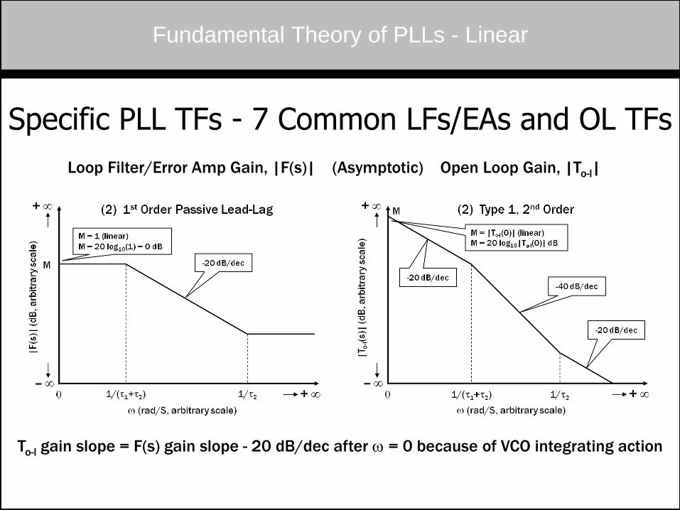
Specific PLL TFs - 7 Common LFs/EAs and OL TFs
To-l gain slope = F(s) gain slope - 20 dB/dec after w = 0 because of VCO integrating action
Loop Filter/Error Amp Gain, |F(s)| (Asymptotic) Open Loop Gain, |To-l|
Fundamental Theory of PLLs - Linear
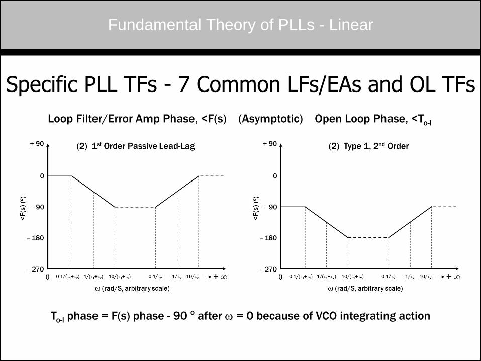
Specific PLL TFs - 7 Common LFs/EAs and OL TFs
Loop Filter/Error Amp Phase, <F(s) (Asymptotic) Open Loop Phase, <To-l
To-l phase = F(s) phase - 90 o after w = 0 because of VCO integrating action
Fundamental Theory of PLLs - Linear
Specific PLL TFs - 7 Common LFs/EAs and OL TFs
To-l gain slope = F(s) gain slope - 20 dB/dec after w = 0 because of VCO integrating action
Loop Filter/Error Amp Gain, |F(s)| (Asymptotic) Open Loop Gain, |To-l|
Fundamental Theory of PLLs - Linear
Specific PLL TFs - 7 Common LFs/EAs and OL TFs
Loop Filter/Error Amp Phase, <F(s) (Asymptotic) Open Loop Phase, <To-l
To-l phase = F(s) phase - 90 o after w = 0 because of VCO integrating action

Fundamental Theory of PLLs - Linear
Specific PLL TFs - 7 Common LFs/EAs and OL TFs
To-l gain slope = F(s) gain slope - 20 dB/dec after w = 0 because of VCO integrating action
Loop Filter/Error Amp Gain, |F(s)| (Asymptotic) Open Loop Gain, |To-l|

Fundamental Theory of PLLs - Linear
Specific PLL TFs - 7 Common LFs/EAs and OL TFs
Loop Filter/Error Amp Phase, <F(s) (Asymptotic) Open Loop Phase, <To-l
To-l phase = F(s) phase - 90 o after w = 0 because of VCO integrating action
Fundamental Theory of PLLs - Linear
Specific PLL TFs - 7 Common LFs/EAs and OL TFs
To-l gain slope = F(s) gain slope - 20 dB/dec after w = 0 because of VCO integrating action
Loop Filter/Error Amp Gain, |F(s)| (Asymptotic) Open Loop Gain, |To-l|
Fundamental Theory of PLLs - Linear
Specific PLL TFs - 7 Common LFs/EAs and OL TFs
Loop Filter/Error Amp Phase, <F(s) (Asymptotic) Open Loop Phase, <To-l
To-l phase = F(s) phase - 90 o after w = 0 because of VCO integrating action

Fundamental Theory of PLLs - Linear
Specific PLL TFs - 7 Common LFs/EAs and OL TFs
To-l gain slope = F(s) gain slope - 20 dB/dec after w = 0 because of VCO integrating action
Loop Filter/Error Amp Gain, |F(s)| (Asymptotic) Open Loop Gain, |To-l|

Fundamental Theory of PLLs - Linear
Specific PLL TFs - 7 Common LFs/EAs and OL TFs
Loop Filter/Error Amp Phase, <F(s) (Asymptotic) Open Loop Phase, <To-l
To-l phase = F(s) phase - 90 o after w = 0 because of VCO integrating action
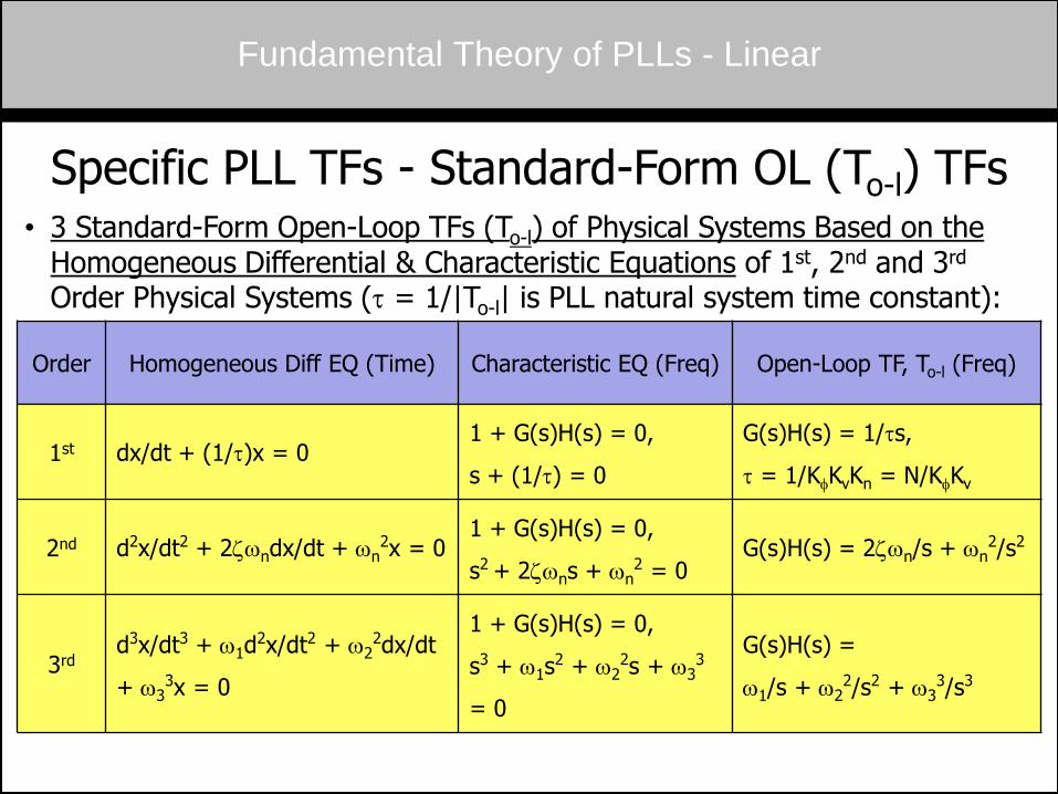
Specific PLL TFs - Standard-Form OL (To-l) TFs
• 3 Standard-Form Open-Loop TFs (To-l) of Physical Systems Based on the Homogeneous Differential & Characteristic Equations of 1st, 2nd and 3rd Order Physical Systems ( = 1/|To-l| is PLL natural system time constant):
Order Homogeneous Diff EQ (Time) Characteristic EQ (Freq) Open-Loop TF, To-l (Freq)
1st dx/dt + (1/)x = 0 1 + G(s)H(s) = 0,
s + (1/) = 0
G(s)H(s) = 1/s,
= 1/KfKvKn = N/KfKv
2nd d2x/dt2 + 2zwndx/dt + wn2x = 0
1 + G(s)H(s) = 0,
s2 + 2zwns + wn2 = 0
G(s)H(s) = 2zwn/s + wn2/s2
3rd d3x/dt3 + w1d
2x/dt2 + w22dx/dt
+ w33x = 0
1 + G(s)H(s) = 0,
s3 + w1s2 + w2
2s + w33
= 0
G(s)H(s) =
w1/s + w22/s2 + w3
3/s3
Fundamental Theory of PLLs - Linear
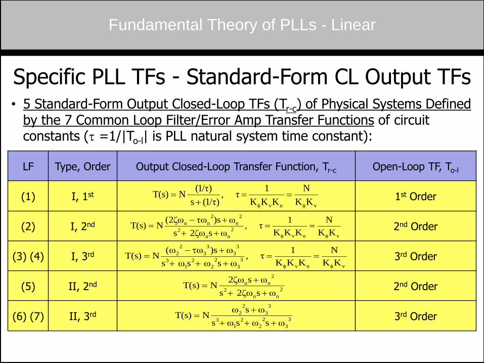
Specific PLL TFs - Standard-Form CL Output TFs
• 5 Standard-Form Output Closed-Loop TFs (Tr-c) of Physical Systems Defined by the 7 Common Loop Filter/Error Amp Transfer Functions of circuit constants ( =1/|To-l| is PLL natural system time constant):
LF Type, Order Output Closed-Loop Transfer Function, Tr-c Open-Loop TF, To-l
(1) I, 1st 1st Order
(2) I, 2nd 2nd Order
(3) (4) I, 3rd 3rd Order
(5) II, 2nd 2nd Order
(6) (7) II, 3rd 3rd Order
vnv KK
N
KKK
1, τ
)/τ1( s
)/τ1(NT(s)
ff
vnv
2
nn
2
2
n
2
nn
KK
N
KKK
1, τ
ωsζω2 s
ω)sτωζω2(NT(s)
ff
2
nn
2
2
nn
ωsζω2 s
ωsζω2NT(s)
Fundamental Theory of PLLs - Linear
3
3
2
2
2
1
3
3
3
2
2
ωsω sω s
ωsωNT(s)
vnv
3
3
2
2
2
1
3
3
3
3
3
2
2
KK
N
KKK
1τ ,
ωs ωs ωs
ωs)ωω(NT(s)
ff
Fundamental Theory of PLLs - Linear
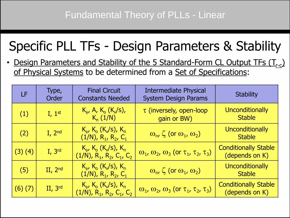
Specific PLL TFs - Design Parameters & Stability
• Design Parameters and Stability of the 5 Standard-Form CL Output TFs (Tr-c) of Physical Systems to be determined from a Set of Specifications:
LF
Type, Order
Final Circuit Constants Needed
Intermediate Physical System Design Params
Stability
(1) I, 1st Kf, A, Ko (Kv/s),
Kn (1/N) (inversely, open-loop
gain or BW)
Unconditionally Stable
(2) I, 2nd Kf, Ko (Kv/s), Kn (1/N), R1, R2, C1
wn, z (or w1, w2) Unconditionally
Stable
(3) (4) I, 3rd Kf, Ko (Kv/s), Kn
(1/N), R1, R2, C1, C2 w1, w2, w3 (or 1, 2, 3)
Conditionally Stable (depends on K)
(5) II, 2nd Kf, Ko (Kv/s), Kn (1/N), R1, R2, C1
wn, z (or w1, w2) Unconditionally
Stable
(6) (7) II, 3rd Kf, Ko (Kv/s), Kn
(1/N), R1, R2, C1, C2 w1, w2, w3 (or 1, 2, 3)
Conditionally Stable (depends on K)
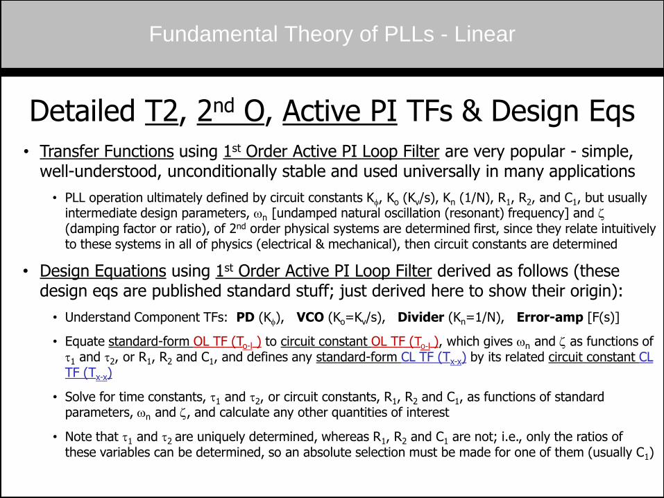
Detailed T2, 2nd O, Active PI TFs & Design Eqs
• Transfer Functions using 1st Order Active PI Loop Filter are very popular - simple, well-understood, unconditionally stable and used universally in many applications
• PLL operation ultimately defined by circuit constants Kf, Ko (Kv/s), Kn (1/N), R1, R2, and C1, but usually intermediate design parameters, wn [undamped natural oscillation (resonant) frequency] and z (damping factor or ratio), of 2nd order physical systems are determined first, since they relate intuitively to these systems in all of physics (electrical & mechanical), then circuit constants are determined
• Design Equations using 1st Order Active PI Loop Filter derived as follows (these design eqs are published standard stuff; just derived here to show their origin):
• Understand Component TFs: PD (Kf), VCO (Ko=Kv/s), Divider (Kn=1/N), Error-amp [F(s)]
• Equate standard-form OL TF (To-l ) to circuit constant OL TF (To-l ), which gives wn and z as functions of 1 and 2, or R1, R2 and C1, and defines any standard-form CL TF (Tx-x) by its related circuit constant CL TF (Tx-x)
• Solve for time constants, 1 and 2, or circuit constants, R1, R2 and C1, as functions of standard parameters, wn and z, and calculate any other quantities of interest
• Note that 1 and 2 are uniquely determined, whereas R1, R2 and C1 are not; i.e., only the ratios of these variables can be determined, so an absolute selection must be made for one of them (usually C1)
Fundamental Theory of PLLs - Linear
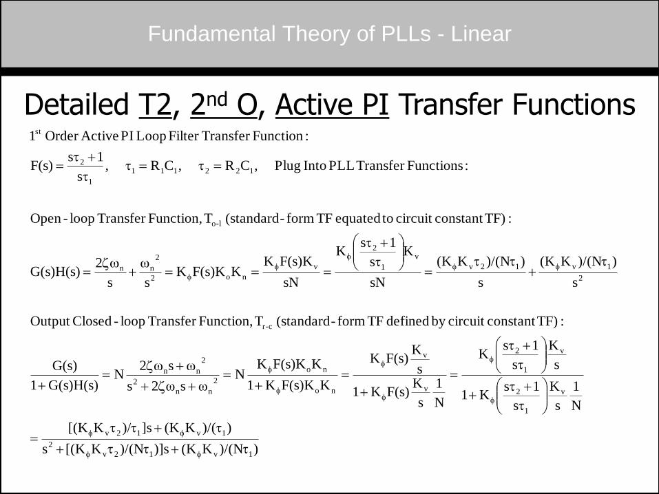
Detailed T2, 2nd O, Active PI Transfer Functions
))/(NK(K)]s)/(NK(K[s
))/(K(K]s)/K[(K
N
1
s
K
s
1sK1
s
K
s
1sK
N
1
s
KF(s)K1
s
KF(s)K
KF(s)KK1
KF(s)KKN
ωsω2s
ωsω2N
G(s)H(s)1
G(s)
:TF)constant circuit by defined TF form-(standard T Function,Transfer loop-ClosedOutput
s
))/(NK(K
s
))/(NK(K
sN
Ks
1sK
sN
F(s)KKKF(s)KK
s
ω
s
2G(s)H(s)
:TF)constant circuit toequated TF form-(standard T Function,Transfer loop-Open
:FunctionsTransfer PLL Into Plug ,CR ,CR ,s
1sF(s)
:FunctionTransfer Filter Loop PI ActiveOrder 1
1v12v
2
1v12v
v
1
2
v
1
2
v
v
no
no
2
nn
2
2
nn
c-r
2
1v12v
v
1
2
v
no2
2
nn
l-o
122111
1
2
st
z
z
zw
ff
ff
f
f
f
f
f
f
ff
f
f
f
Fundamental Theory of PLLs - Linear
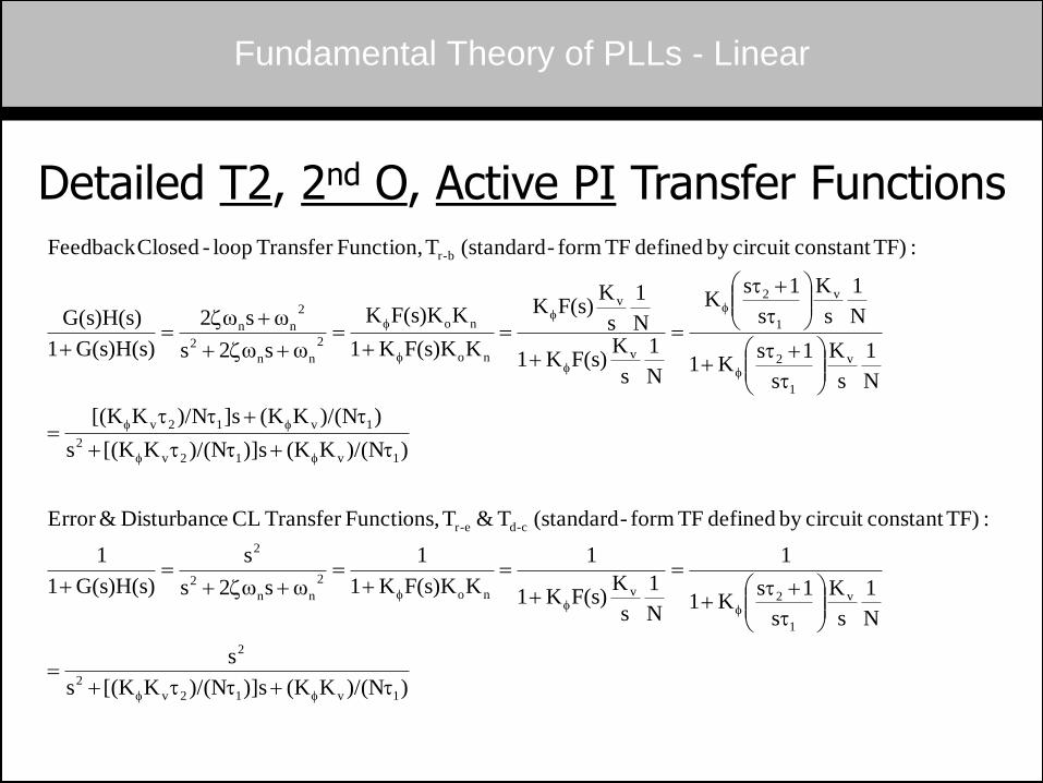
Detailed T2, 2nd O, Active PI Transfer Functions
Fundamental Theory of PLLs - Linear
))/(NK(K)]s)/(NK(K[s
s
N
1
s
K
s
1sK1
1
N
1
s
KF(s)K1
1
KF(s)KK1
1
ωsω2s
s
G(s)H(s)1
1
:TF)constant circuit by defined TF form-(standard T &T Functions,Transfer CL eDisturbanc &Error
))/(NK(K)]s)/(NK(K[s
))/(NK(K]s)/NK[(K
N
1
s
K
s
1sK1
N
1
s
K
s
1sK
N
1
s
KF(s)K1
N
1
s
KF(s)K
KF(s)KK1
KF(s)KK
ωsω2s
ωsω2
G(s)H(s)1
G(s)H(s)
:TF)constant circuit by defined TF form-(standard T Function,Transfer loop-ClosedFeedback
1v12v
2
2
v
1
2vno
2
nn
2
2
c-de-r
1v12v
2
1v12v
v
1
2
v
1
2
v
v
no
no
2
nn
2
2
nn
b-r
z
z
z
ff
fff
ff
ff
f
f
f
f
f
f
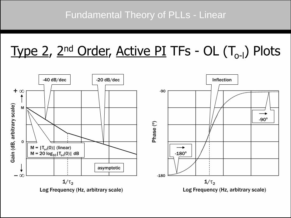
Type 2, 2nd Order, Active PI TFs - OL (To-l) Plots
Fundamental Theory of PLLs - Linear
1/2
0
Log Frequency (Hz, arbitrary scale)
-20 dB/dec -40 dB/dec
Ph
ase
(o)
-180
-90
Log Frequency (Hz, arbitrary scale)
1/2
Inflection
M = |To-l(0)| (linear)
M = 20 log10|To-l(0)| dB
-180o
-90o
Ga
in (
dB
, a
rbit
rary
sca
le)
--
M
+
asymptotic
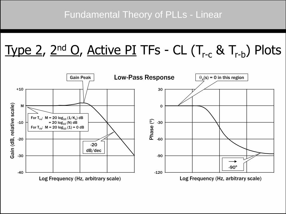
Type 2, 2nd O, Active PI TFs - CL (Tr-c & Tr-b) Plots
Fundamental Theory of PLLs - Linear
Ph
ase
(o)
Ga
in (
dB
, re
lati
ve s
ca
le)
M 0
Log Frequency (Hz, arbitrary scale) Log Frequency (Hz, arbitrary scale)
Low-Pass Response
+10
-10
-20
-30
-40
30
-30
-60
-90
-120
-20
dB/dec
-90o
For Ti-o: M = 20 log10 (1/Kn) dB
= 20 log10 (N) dB
For Ti-b: M = 20 log10 (1) = 0 dB
qe(s) = 0 in this region Gain Peak
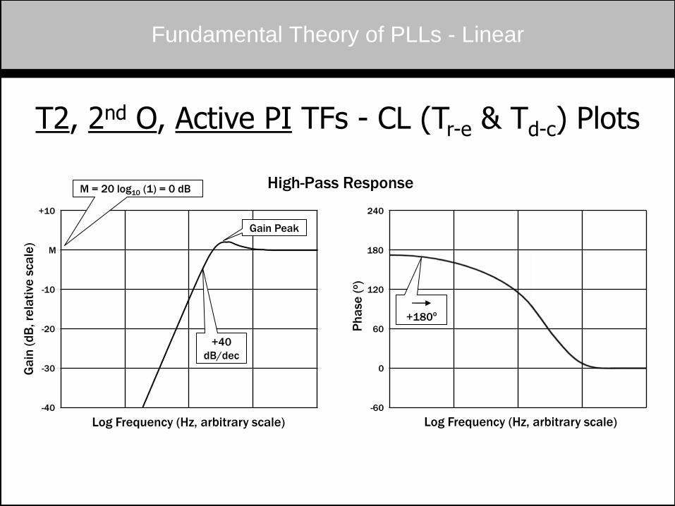
T2, 2nd O, Active PI TFs - CL (Tr-e & Td-c) Plots
Fundamental Theory of PLLs - Linear
Ph
ase
(o)
Log Frequency (Hz, arbitrary scale) Log Frequency (Hz, arbitrary scale)
High-Pass Response
M
-10
-20
-30
-40
180
240
120
60
0
-60
+40
dB/dec
+180o
+10
Gain Peak
Ga
in (
dB
, re
lati
ve s
ca
le)
M = 20 log10 (1) = 0 dB
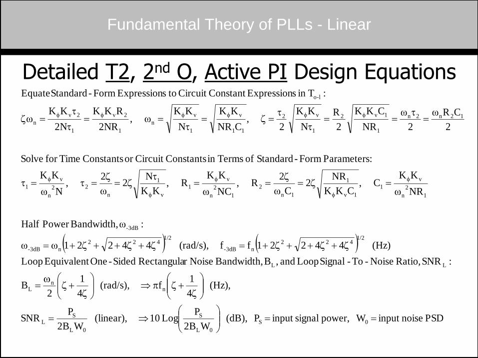
Detailed T2, 2nd O, Active PI Design Equations
PSD noiseinput Wpower, signalinput P (dB), WB2
PLog 10 (linear),
WB2
PSNR
,(Hz) 4
1f (rad/s),
4
1
2B
:SNR Ratio, Noise-To-Signal Loop and ,B Bandwidth, Noiser Rectangula Sided-One Equivalent Loop
(Hz) 44221ff (rad/s), 44221ωω
:ω Bandwidth,Power Half
NRω
KKC ,
CKK
NR2
Cω
2R ,
NCω
KKR ,
KK
N2
ω
2 ,
Nω
KK
:Parameters Form-Standard of Termsin ConstantsCircuit or Constants Timefor Solve
2
CRω
2
ω
NR
CKK
2
R
N
KK
2 ,
CNR
KK
N
KKω ,
R2N
RKK
2N
KKω
:Tin sExpressionConstant Circuit tosExpression Form-Standard Equate
0S
0L
S
0L
SL
nn
L
LL
1/2422
ndB3-
1/2422
ndB3-
dB3-
1
2
n
v
1
1v
1
1n
2
1
2
n
v
1
v
1
n
22
n
v
1
12n2n
1
1v2
1
v2
11
v
1
v
n
1
2v
1
2v
n
l-o
zzp
zz
w
zzzzzz
zz
zz
z
z
f
f
f
f
f
ffffff
Fundamental Theory of PLLs - Linear
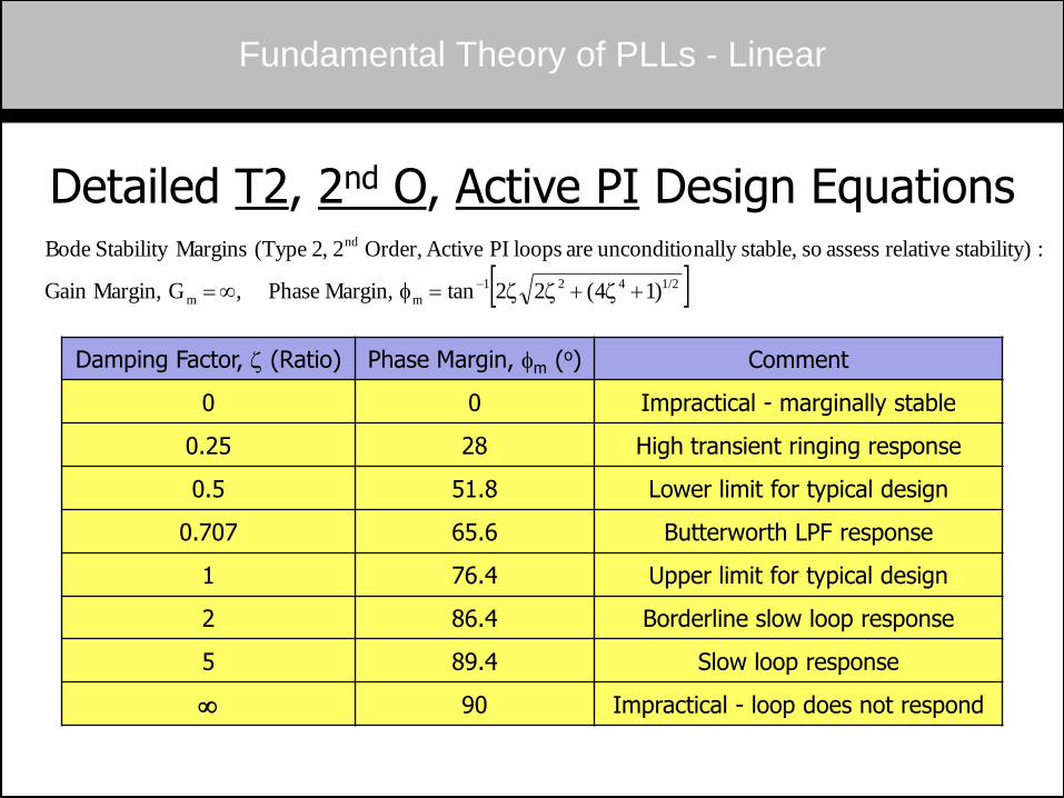
Detailed T2, 2nd O, Active PI Design Equations
1/2421
mm
nd
)14(22tan Margin, Phase , G Margin,Gain
:stability) relative assess so stable,nally unconditio are loops PI Active Order, 2 2, (Type MarginsStability Bode
zzzf
Damping Factor, z (Ratio) Phase Margin, fm (o) Comment
0 0 Impractical - marginally stable
0.25 28 High transient ringing response
0.5 51.8 Lower limit for typical design
0.707 65.6 Butterworth LPF response
1 76.4 Upper limit for typical design
2 86.4 Borderline slow loop response
5 89.4 Slow loop response
90 Impractical - loop does not respond
Fundamental Theory of PLLs - Linear
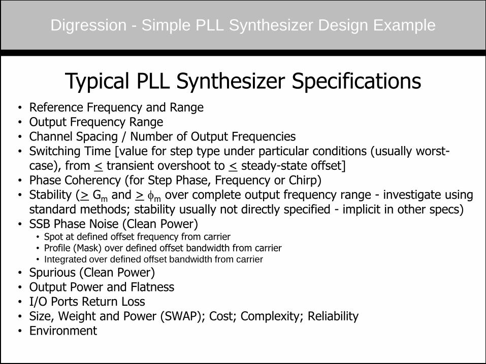
Digression - Simple PLL Synthesizer Design Example
Typical PLL Synthesizer Specifications
• Reference Frequency and Range • Output Frequency Range • Channel Spacing / Number of Output Frequencies • Switching Time [value for step type under particular conditions (usually worst-
case), from < transient overshoot to < steady-state offset] • Phase Coherency (for Step Phase, Frequency or Chirp) • Stability (> Gm and > fm over complete output frequency range - investigate using
standard methods; stability usually not directly specified - implicit in other specs) • SSB Phase Noise (Clean Power)
• Spot at defined offset frequency from carrier • Profile (Mask) over defined offset bandwidth from carrier • Integrated over defined offset bandwidth from carrier
• Spurious (Clean Power) • Output Power and Flatness • I/O Ports Return Loss • Size, Weight and Power (SWAP); Cost; Complexity; Reliability • Environment
Digression - Simple PLL Synthesizer Design Example
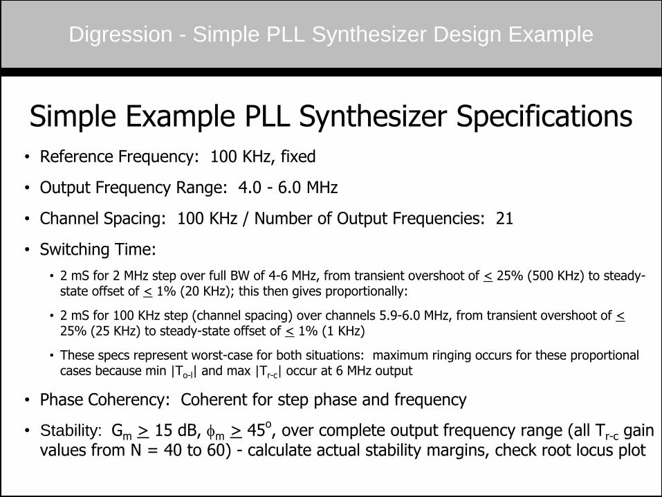
Simple Example PLL Synthesizer Specifications
• Reference Frequency: 100 KHz, fixed
• Output Frequency Range: 4.0 - 6.0 MHz
• Channel Spacing: 100 KHz / Number of Output Frequencies: 21
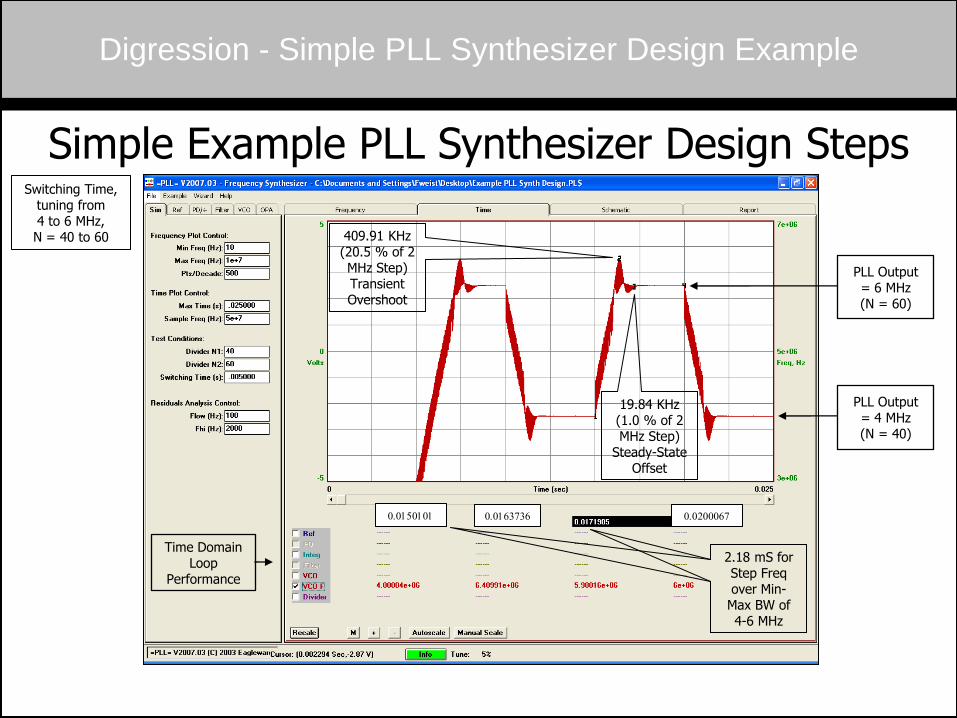
• Switching Time:
• 2 mS for 2 MHz step over full BW of 4-6 MHz, from transient overshoot of < 25% (500 KHz) to steady-state offset of < 1% (20 KHz); this then gives proportionally:
• 2 mS for 100 KHz step (channel spacing) over channels 5.9-6.0 MHz, from transient overshoot of < 25% (25 KHz) to steady-state offset of < 1% (1 KHz)
• These specs represent worst-case for both situations: maximum ringing occurs for these proportional cases because min |To-l| and max |Tr-c| occur at 6 MHz output
• Phase Coherency: Coherent for step phase and frequency
• Stability: Gm > 15 dB, fm > 45o, over complete output frequency range (all Tr-c gain
values from N = 40 to 60) - calculate actual stability margins, check root locus plot
Digression - Simple PLL Synthesizer Design Example
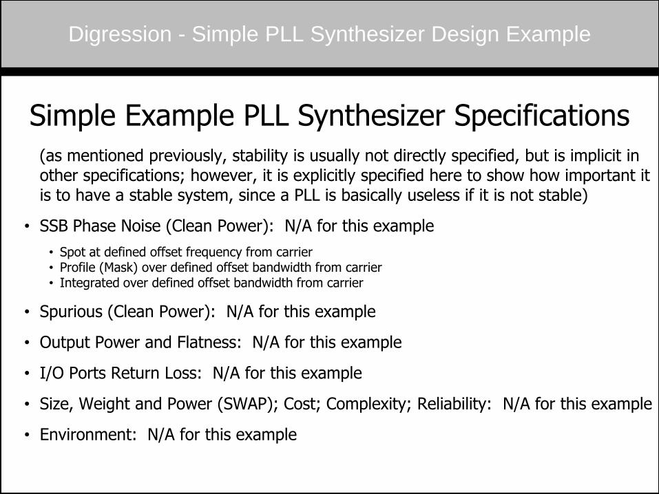
Simple Example PLL Synthesizer Specifications
(as mentioned previously, stability is usually not directly specified, but is implicit in other specifications; however, it is explicitly specified here to show how important it is to have a stable system, since a PLL is basically useless if it is not stable)
• SSB Phase Noise (Clean Power): N/A for this example
• Spot at defined offset frequency from carrier • Profile (Mask) over defined offset bandwidth from carrier • Integrated over defined offset bandwidth from carrier
• Spurious (Clean Power): N/A for this example
• Output Power and Flatness: N/A for this example
• I/O Ports Return Loss: N/A for this example
• Size, Weight and Power (SWAP); Cost; Complexity; Reliability: N/A for this example
• Environment: N/A for this example
Digression - Simple PLL Synthesizer Design Example
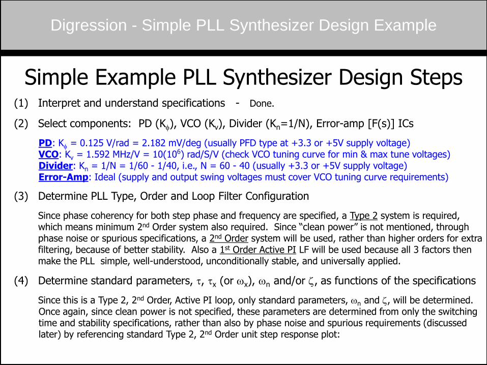
Simple Example PLL Synthesizer Design Steps (1) Interpret and understand specifications - Done.
(2) Select components: PD (Kf), VCO (Kv), Divider (Kn=1/N), Error-amp [F(s)] ICs
PD: Kf = 0.125 V/rad = 2.182 mV/deg (usually PFD type at +3.3 or +5V supply voltage) VCO: Kv = 1.592 MHz/V = 10(106) rad/S/V (check VCO tuning curve for min & max tune voltages) Divider: Kn = 1/N = 1/60 - 1/40, i.e., N = 60 - 40 (usually +3.3 or +5V supply voltage) Error-Amp: Ideal (supply and output swing voltages must cover VCO tuning curve requirements)
(3) Determine PLL Type, Order and Loop Filter Configuration
Since phase coherency for both step phase and frequency are specified, a Type 2 system is required, which means minimum 2nd Order system also required. Since “clean power” is not mentioned, through phase noise or spurious specifications, a 2nd Order system will be used, rather than higher orders for extra filtering, because of better stability. Also a 1st Order Active PI LF will be used because all 3 factors then make the PLL simple, well-understood, unconditionally stable, and universally applied.
(4) Determine standard parameters, , x (or wx), wn and/or z, as functions of the specifications
Since this is a Type 2, 2nd Order, Active PI loop, only standard parameters, wn and z, will be determined. Once again, since clean power is not specified, these parameters are determined from only the switching time and stability specifications, rather than also by phase noise and spurious requirements (discussed later) by referencing standard Type 2, 2nd Order unit step response plot:
Digression - Simple PLL Synthesizer Design Example
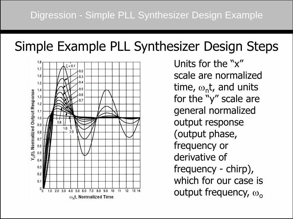
Simple Example PLL Synthesizer Design Steps
Units for the “x” scale are normalized time, wnt, and units for the “y” scale are general normalized output response (output phase, frequency or derivative of frequency - chirp), which for our case is output frequency, wo
Digression - Simple PLL Synthesizer Design Example
Simple Example PLL Synthesizer Design Steps
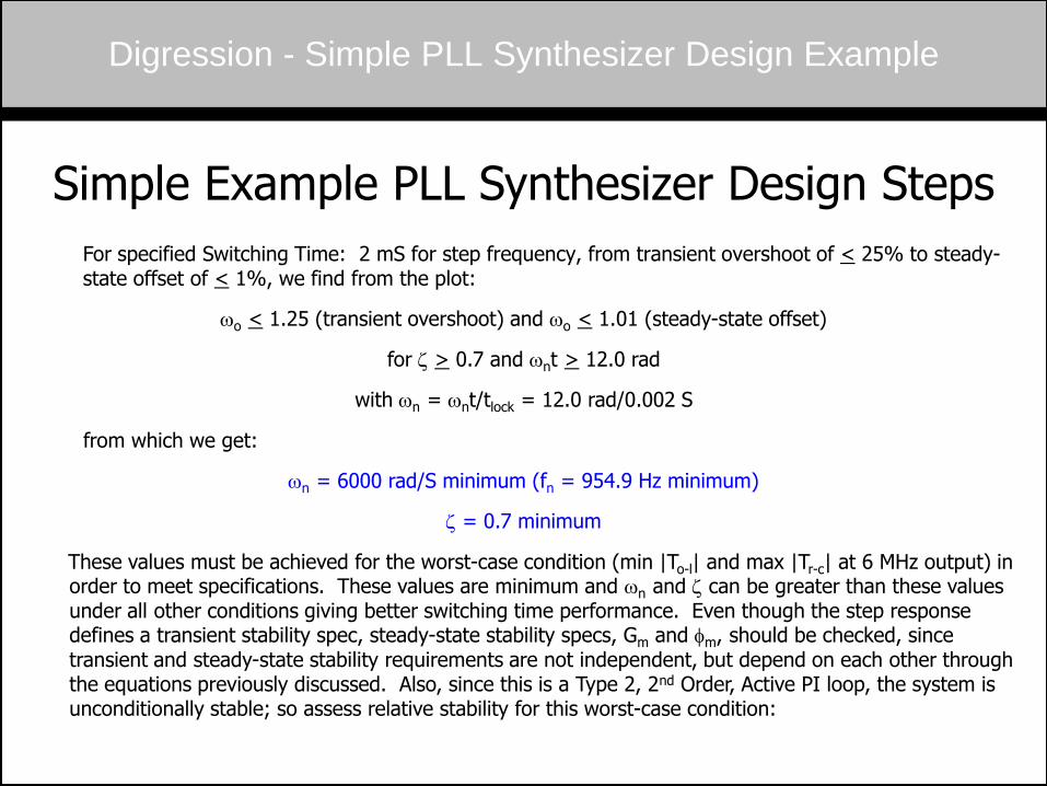
For specified Switching Time: 2 mS for step frequency, from transient overshoot of < 25% to steady-state offset of < 1%, we find from the plot:
wo < 1.25 (transient overshoot) and wo < 1.01 (steady-state offset)
for z > 0.7 and wnt > 12.0 rad
with wn = wnt/tlock = 12.0 rad/0.002 S
from which we get:
wn = 6000 rad/S minimum (fn = 954.9 Hz minimum)
z = 0.7 minimum
These values must be achieved for the worst-case condition (min |To-l| and max |Tr-c| at 6 MHz output) in order to meet specifications. These values are minimum and wn and z can be greater than these values under all other conditions giving better switching time performance. Even though the step response defines a transient stability spec, steady-state stability specs, Gm and fm, should be checked, since transient and steady-state stability requirements are not independent, but depend on each other through the equations previously discussed. Also, since this is a Type 2, 2nd Order, Active PI loop, the system is unconditionally stable; so assess relative stability for this worst-case condition:
Digression - Simple PLL Synthesizer Design Example
Simple Example PLL Synthesizer Design Steps
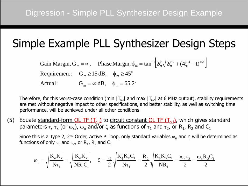
Therefore, for this worst-case condition (min |To-l| and max |Tr-c| at 6 MHz output), stability requirements are met without negative impact to other specifications, and better stability, as well as switching time performance, will be achieved under all other conditions
(5) Equate standard-form OL TF (To-l) to circuit constant OL TF (To-l), which gives standard parameters , x (or wx), wn and/or z as functions of 1 and 2, or R1, R2 and C1
Since this is a Type 2, 2nd Order, Active PI loop, only standard variables wn and z will be determined as functions of only 1 and 2, or R1, R2 and C1
2
CRω
2
ω
NR
CKK
2
R
N
CKK
2 ,
CNR
KK
N
KKω 12n2n
1
1v2
1
1v2
11
v
1
v
n
z
ffff
o
mm
o
mm
1/2421
mm
65.2 dB, G :Actual
45 dB, 15 G :tRequiremen
)14(22tan Margin, Phase , G Margin,Gain
f
f
zzzf
Digression - Simple PLL Synthesizer Design Example
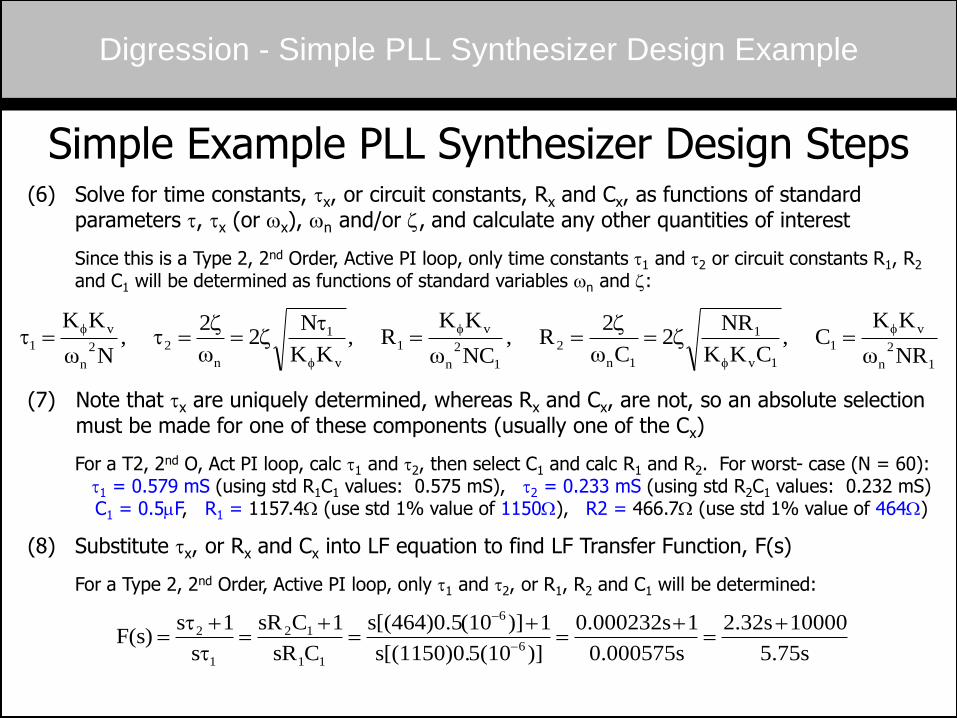
Simple Example PLL Synthesizer Design Steps (6) Solve for time constants, x, or circuit constants, Rx and Cx, as functions of standard
parameters , x (or wx), wn and/or z, and calculate any other quantities of interest
Since this is a Type 2, 2nd Order, Active PI loop, only time constants 1 and 2 or circuit constants R1, R2 and C1 will be determined as functions of standard variables wn and z:
(7) Note that x are uniquely determined, whereas Rx and Cx, are not, so an absolute selection must be made for one of these components (usually one of the Cx)
For a T2, 2nd O, Act PI loop, calc 1 and 2, then select C1 and calc R1 and R2. For worst- case (N = 60): 1 = 0.579 mS (using std R1C1 values: 0.575 mS), 2 = 0.233 mS (using std R2C1 values: 0.232 mS) C1 = 0.5mF, R1 = 1157.4W (use std 1% value of 1150W), R2 = 466.7W (use std 1% value of 464W)
(8) Substitute x, or Rx and Cx into LF equation to find LF Transfer Function, F(s)
For a Type 2, 2nd Order, Active PI loop, only 1 and 2, or R1, R2 and C1 will be determined:
1
2
n
v
1
1v
1
1n
2
1
2
n
v
1
v
1
n
22
n
v
1NRω
KKC ,
CKK
NR2
Cω
2R ,
NCω
KKR ,
KK
N2
ω
2 ,
Nω
KK f
f
f
f
fz
z
z
z
5.75s
100002.32s
0.000575s
10.000232s
)]5(10s[(1150)0.
1)](10s[(464)0.5
CsR
1CsR
s
1sF(s)
6
6
11
12
1
2
Digression - Simple PLL Synthesizer Design Example
qb(s)
Phase Detector
or
Phase/Frequency
Detector
Loop Filter or
Loop
Filter/Error
Amp
Phase/Frequency
Divider or
Translator (mixer,
N = 1 only)
VCO Phase
Disturbance
Signal
Simple Example PLL Synthesizer Design Steps
(9) Substitute all building block transfer functions into model to properly configure PLL
5.75s
100002.32s
F(s)
V/rad
125.0
K f
rad/S/V
)10(10
s
KK
6
vo
40
1 to
60
1
N
1Kn
qe(s)
W
W
m
464R
1150R
F 5.0C
mS 232.0
mS 0.575
2
1
1
2
1
qb(s)
Phase Detector
or
Phase/Frequency
Detector
Loop Filter or
Loop
Filter/Error
Amp
Frequency/Phase
Divider or
Translator (mixer,
N = 1 only)
Phase
Disturbance
Signal
qe(s)
S S
VCO
qd(s)
qc(s) qr(s)
+
- +
-
Digression - Simple PLL Synthesizer Design Example
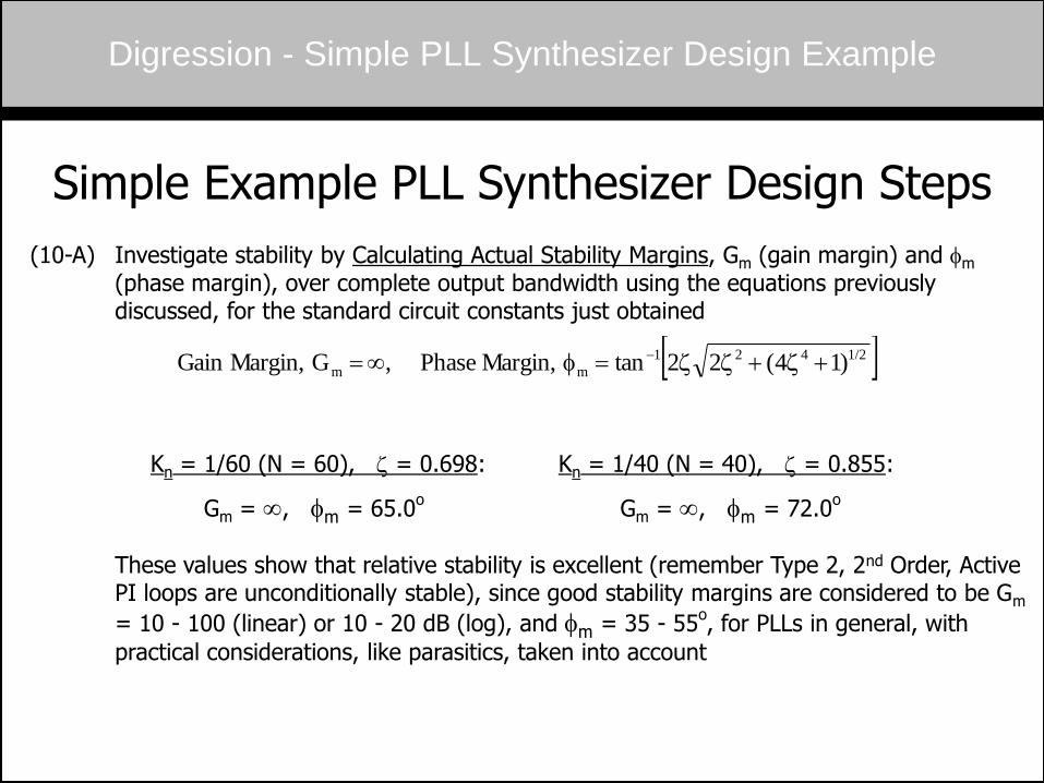
Simple Example PLL Synthesizer Design Steps
(10-A) Investigate stability by Calculating Actual Stability Margins, Gm (gain margin) and fm (phase margin), over complete output bandwidth using the equations previously discussed, for the standard circuit constants just obtained
Kn = 1/60 (N = 60), z = 0.698: Kn = 1/40 (N = 40), z = 0.855:
Gm = , fm = 65.0o Gm = , fm = 72.0
o
These values show that relative stability is excellent (remember Type 2, 2nd Order, Active PI loops are unconditionally stable), since good stability margins are considered to be Gm
= 10 - 100 (linear) or 10 - 20 dB (log), and fm = 35 - 55o, for PLLs in general, with
practical considerations, like parasitics, taken into account
1/2421
mm )14(22tan Margin, Phase , G Margin,Gain zzzf
Digression - Simple PLL Synthesizer Design Example
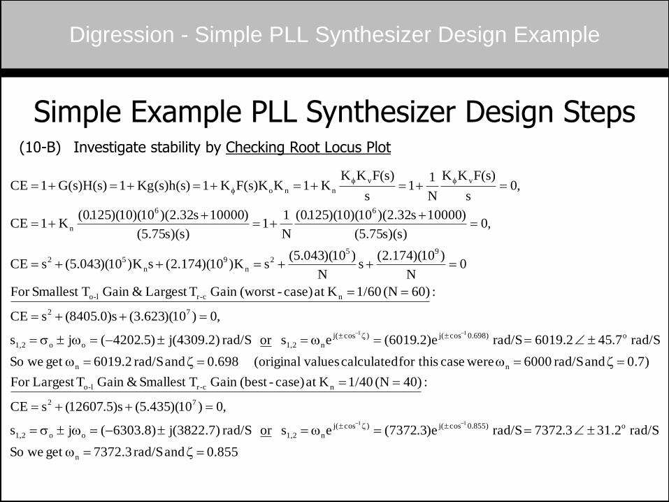
Simple Example PLL Synthesizer Design Steps (10-B) Investigate stability by Checking Root Locus Plot
0.855 and rad/S 7372.3 get weSo
rad/S 31.2 3.7372rad/S e)3.7372(es or rad/S j(3822.7)6303.8)(js
,0)10)(435.5(s)5.12607(sCE
:0)4(N 1/40Kat case)-(bestGain TSmallest &Gain TLargest For
0.7) and rad/S 6000 werecase for this calculated values(original 0.698 and rad/S 6019.2 get weSo
rad/S 7.45 6019.2rad/S e)2.6019(es or rad/S j(4309.2))5.4202(js
,0)10)(623.3(s)0.8405(sCE
:0)6(N 1/60Kat case)-(worstGain TLargest &Gain TSmallest For
0N
)10)(174.2(s
N
)10)(043.5(sK)10)(174.2(sK)10)(043.5(sCE
,0)s)(s75.5(
)10000s32.2)(10)(10)(125.0(
N
11
)s)(s75.5(
)10000s32.2)(10)(10)(125.0(K1CE
,0s
F(s)KK
N
11
s
)s(FKKK1KF(s)KK1(s)h(s)Kg1G(s)H(s)1CE
n
o)855.0cos(j)cos(j
n1,2oo1,2
72
nc-rl-o
nn
o)698.0cos(j)cos(j
n1,2oo1,2
72
nc-rl-o
952
n
9
n
52
66
n
vv
nno
11
11
zw
wws
zwzw
wws
z
z
ff
f
Digression - Simple PLL Synthesizer Design Example
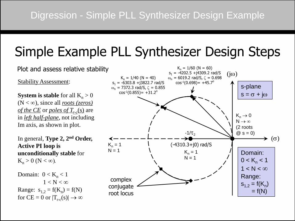
(s)
(jw)
Kn 0
N
(2 roots
@ s = 0)
Kn = 1
N = 1
(-4310.3+j0) rad/S
Simple Example PLL Synthesizer Design Steps
Plot and assess relative stability
Kn = 1
N = 1
complex conjugate root locus
Stability Assessment:
System is stable for all Kn > 0
(N < ), since all roots (zeros)
of the CE or poles of Tr-c(s) are
in left half-plane, not including
Im axis, as shown in plot.
In general, Type 2, 2nd Order,
Active PI loop is
unconditionally stable for
Kn > 0 (N <
Domain: 0 < Kn < 1
1 < N <
Range: s1,2 = f(Kn) = f(N)
for CE = 0 or |Tr-c(s)|
Kn = 1/60 (N = 60) s1 = -4202.5 +j4309.2 rad/S wn = 6019.2 rad/S, z = 0.698
cos-1(0.698)= +45.7o
Kn = 1/40 (N = 40) s1 = -6303.8 +j3822.7 rad/S wn = 7372.3 rad/S, z = 0.855
cos-1(0.855)= +31.2o
s-plane
s = s + jw
Domain:
0 < Kn < 1
1 < N < Range:
s1,2 = f(Kn)
= f(N)
-1/2
Digression - Simple PLL Synthesizer Design Example
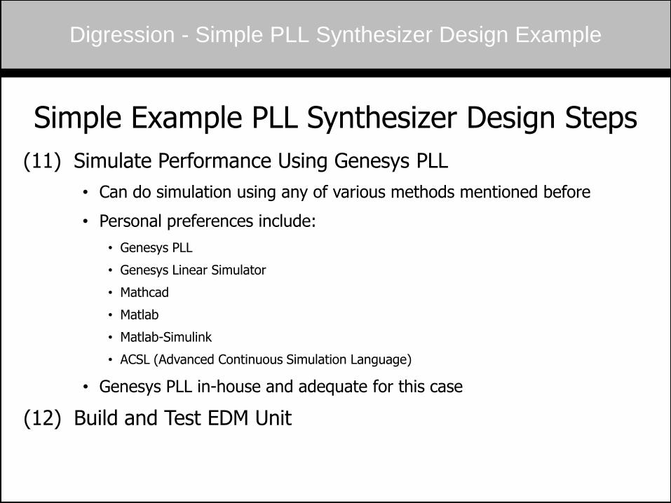
Simple Example PLL Synthesizer Design Steps
(11) Simulate Performance Using Genesys PLL
• Can do simulation using any of various methods mentioned before
• Personal preferences include:
• Genesys PLL
• Genesys Linear Simulator
• Mathcad
• Matlab
• Matlab-Simulink
• ACSL (Advanced Continuous Simulation Language)
• Genesys PLL in-house and adequate for this case
(12) Build and Test EDM Unit

Digression - Simple PLL Synthesizer Design Example
Simple Example PLL Synthesizer Design Steps
10 758578 959401
Peak wn Gain Crossover
Phase Margin, fm = 180 +
(-114.882) = 65.118o
Ideal case - no finite poles & 1 finite zero in To-l (plus 2
poles at w=f=0
& other zero at w=f=)
N = 60, 6 MHz RF Output
Baseband Loop
Performance
No Finite Phase Crossover, Gain Margin, Gm =
Digression - Simple PLL Synthesizer Design Example
Simple Example PLL Synthesizer Design Steps
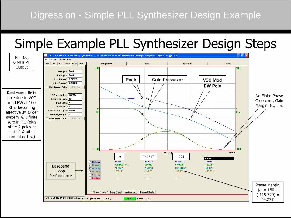
10 765597 147911
Phase Margin, fm = 180 +
(-115.729) = 64.271o
Peak VCO Mod
BW Pole
Gain Crossover
N = 60, 6 MHz RF Output
Real case - finite pole due to VCO mod BW at 100 KHz, becoming
effective 3rd Order system, & 1 finite zero in To-l (plus other 2 poles at w=f=0 & other
zero at w=f=)
Baseband Loop
Performance
No Finite Phase Crossover, Gain Margin, Gm =
Digression - Simple PLL Synthesizer Design Example
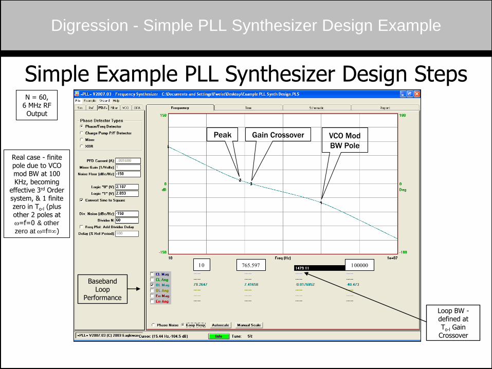
Simple Example PLL Synthesizer Design Steps
10 765597 100000
N = 60, 6 MHz RF Output
Baseband Loop
Performance
Peak VCO Mod
BW Pole
Gain Crossover
Real case - finite pole due to VCO mod BW at 100 KHz, becoming
effective 3rd Order system, & 1 finite zero in To-l (plus other 2 poles at w=f=0 & other
zero at w=f=)
Loop BW - defined at To-l Gain
Crossover

Digression - Simple PLL Synthesizer Design Example
Simple Example PLL Synthesizer Design Steps
10 765597 100000
N = 60, 6 MHz RF Output
Baseband Loop
Performance
VCO Mod
BW Pole
(Inflection)
Gain Crossover
(Phase Margin)
Phase Margin, fm = 180 +
(-115.729) = 64.271o
No Finite Phase Crossover, Gain Margin, Gm =
Real case - finite pole due to VCO mod BW at 100 KHz, becoming
effective 3rd Order system, & 1 finite zero in To-l (plus other 2 poles at w=f=0 & other
zero at w=f=)
Peak
Digression - Simple PLL Synthesizer Design Example
Simple Example PLL Synthesizer Design Steps
765579 959401 147911
N = 60, 6 MHz RF Output
Baseband Loop
Performance
Peak wn
Gain Crossover
w-3dB
Real case - finite pole due to VCO mod BW at 100 KHz, becoming
effective 3rd Order system, & 1 finite zero in To-l (plus other 2 poles at w=f=0 & other
zero at w=f=)
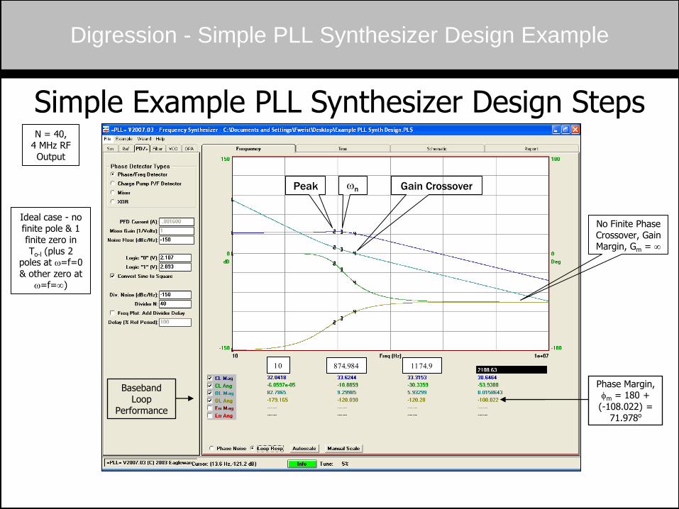
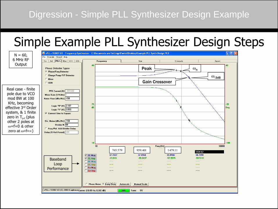
Digression - Simple PLL Synthesizer Design Example
Simple Example PLL Synthesizer Design Steps
10 874984 11749
Peak wn Gain Crossover
Phase Margin, fm = 180 +
(-108.022) = 71.978o
N = 40, 4 MHz RF Output
Baseband Loop
Performance
Ideal case - no finite pole & 1 finite zero in To-l (plus 2
poles at w=f=0
& other zero at w=f=)
No Finite Phase Crossover, Gain Margin, Gm =

Digression - Simple PLL Synthesizer Design Example
Simple Example PLL Synthesizer Design Steps
10 887156 210863
Phase Margin, fm = 180 +
(-109.23) = 70.77o
Peak VCO Mod
BW Pole
Gain Crossover
N = 40, 4 MHz RF Output
Baseband Loop
Performance
No Finite Phase Crossover, Gain Margin, Gm =
Real case - finite pole due to VCO mod BW at 100 KHz, becoming
effective 3rd Order system, & 1 finite zero in To-l (plus other 2 poles at w=f=0 & other
zero at w=f=)
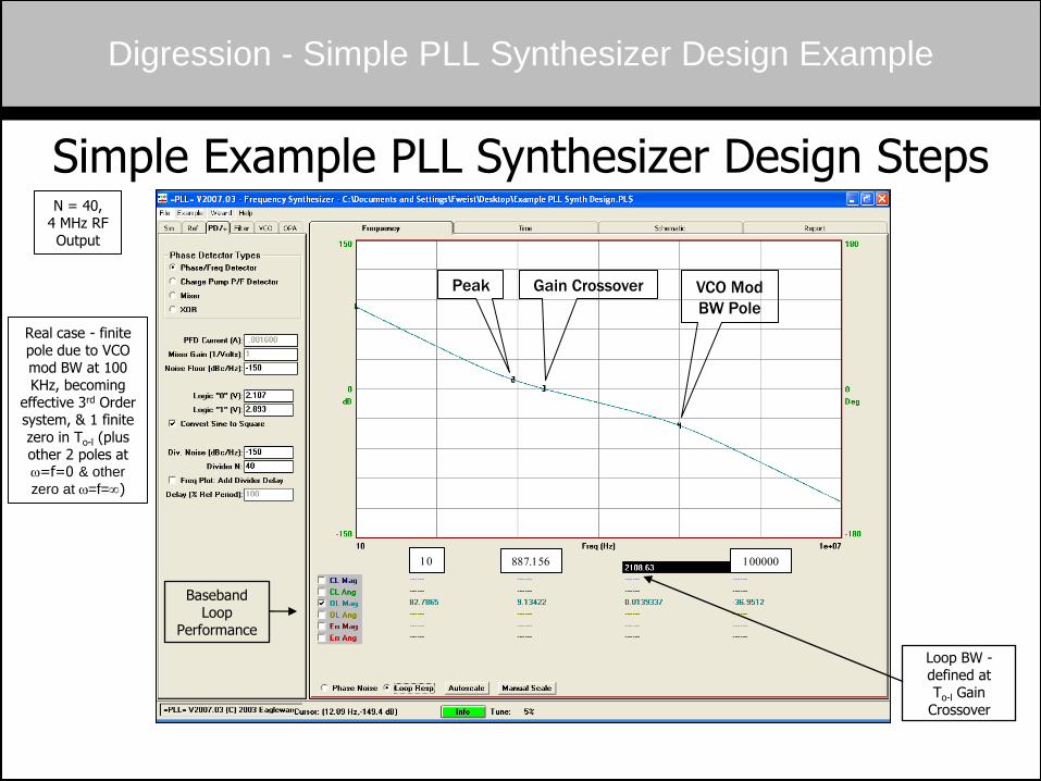
Digression - Simple PLL Synthesizer Design Example
Simple Example PLL Synthesizer Design Steps
10 887156 100000
N = 40, 4 MHz RF Output
Baseband Loop
Performance
VCO Mod
BW Pole
Gain Crossover
Real case - finite pole due to VCO mod BW at 100 KHz, becoming
effective 3rd Order system, & 1 finite zero in To-l (plus other 2 poles at w=f=0 & other
zero at w=f=)
Peak
Loop BW - defined at To-l Gain
Crossover
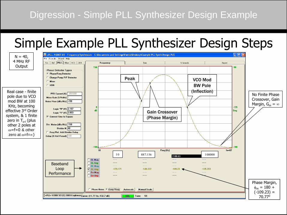
Digression - Simple PLL Synthesizer Design Example
Simple Example PLL Synthesizer Design Steps
10 887156 100000
N = 40, 4 MHz RF Output
Baseband Loop
Performance
VCO Mod
BW Pole
(Inflection)
Gain Crossover
(Phase Margin)
Phase Margin, fm = 180 +
(-109.23) = 70.77o
No Finite Phase Crossover, Gain Margin, Gm =
Real case - finite pole due to VCO mod BW at 100 KHz, becoming
effective 3rd Order system, & 1 finite zero in To-l (plus other 2 poles at w=f=0 & other
zero at w=f=)
Peak
Digression - Simple PLL Synthesizer Design Example
Simple Example PLL Synthesizer Design Steps
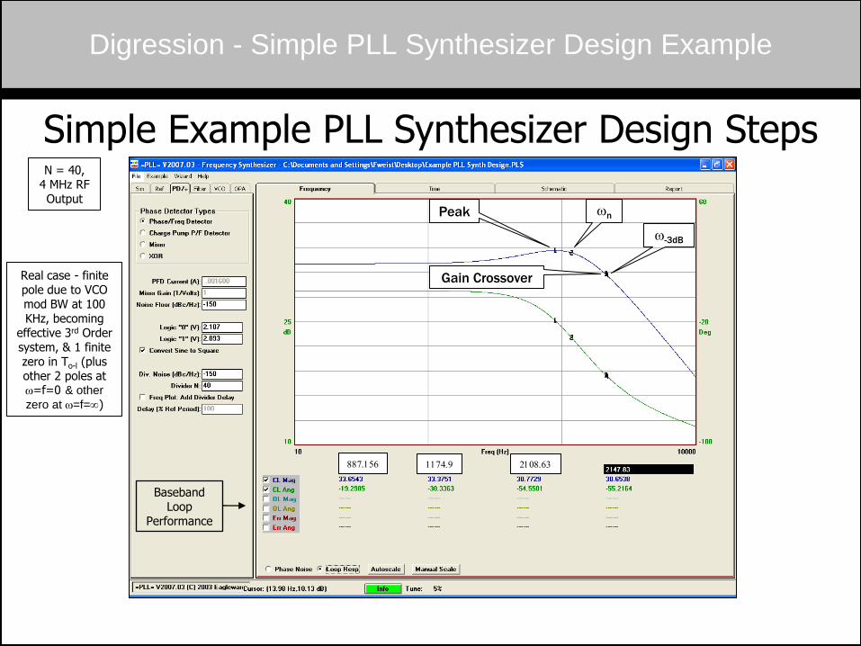
887156 11749 210863
N = 40, 4 MHz RF Output
Baseband Loop
Performance
Peak wn
w-3dB
Real case - finite pole due to VCO mod BW at 100 KHz, becoming
effective 3rd Order system, & 1 finite zero in To-l (plus other 2 poles at w=f=0 & other
zero at w=f=)
Gain Crossover
Digression - Simple PLL Synthesizer Design Example
Simple Example PLL Synthesizer Design Steps
00150101 00163736 00200067
Switching Time, tuning from 4 to 6 MHz, N = 40 to 60
Time Domain Loop
Performance
PLL Output = 6 MHz (N = 60)
PLL Output = 4 MHz (N = 40)
409.91 KHz (20.5 % of 2 MHz Step) Transient Overshoot
19.84 KHz (1.0 % of 2 MHz Step)
Steady-State Offset
2.18 mS for Step Freq over Min-
Max BW of 4-6 MHz
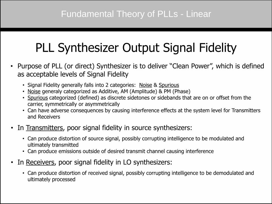
PLL Synthesizer Output Signal Fidelity
• Purpose of PLL (or direct) Synthesizer is to deliver “Clean Power”, which is defined as acceptable levels of Signal Fidelity
• Signal Fidelity generally falls into 2 categories: Noise & Spurious • Noise generaly categorized as Additive, AM (Amplitude) & PM (Phase) • Spurious categorized (defined) as discrete sidetones or sidebands that are on or offset from the
carrier, symmetrically or asymmetrically • Can have adverse consequences by causing interference effects at the system level for Transmitters
and Receivers
• In Transmitters, poor signal fidelity in source synthesizers:
• Can produce distortion of source signal, possibly corrupting intelligence to be modulated and ultimately transmitted
• Can produce emissions outside of desired transmit channel causing interference
• In Receivers, poor signal fidelity in LO synthesizers:
• Can produce distortion of received signal, possibly corrupting intelligence to be demodulated and ultimately processed
Fundamental Theory of PLLs - Linear
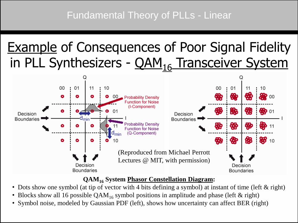
QAM16 System Phasor Constellation Diagram:
• Dots show one symbol (at tip of vector with 4 bits defining a symbol) at instant of time (left & right)
• Blocks show all 16 possible QAM16 symbol positions in amplitude and phase (left & right)
• Symbol noise, modeled by Gaussian PDF (left), shows how uncertainty can affect BER (right)
Example of Consequences of Poor Signal Fidelity in PLL Synthesizers - QAM16 Transceiver System
Fundamental Theory of PLLs - Linear
(Reproduced from Michael Perrott
Lectures @ MIT, with permission)
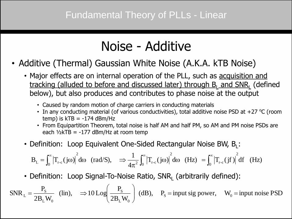
Noise - Additive
• Additive (Thermal) Gaussian White Noise (A.K.A. kTB Noise)
• Major effects are on internal operation of the PLL, such as acquisition and tracking (alluded to before and discussed later) through BL and SNRL (defined below), but also produces and contributes to phase noise at the output
• Caused by random motion of charge carriers in conducting materials • In any conducting material (of various conductivities), total additive noise PSD at +27 oC (room
temp) is kTB = -174 dBm/Hz • From Equipartition Theorem, total noise is half AM and half PM, so AM and PM noise PSDs are
each ½kTB = -177 dBm/Hz at room temp
• Definition: Loop Equivalent One-Sided Rectangular Noise BW, BL:
• Definition: Loop Signal-To-Noise Ratio, SNRL (arbitrarily defined):
(Hz) df)jf(T (Hz) d)j(T4
1 (rad/S), d)j(TB
2
0c-r
2
0c-r2
2
0c-rL
wwp
ww
PSD noiseinput Wpower, siginput P (dB), WB2
PLog 10 (lin),
WB2
PSNR 0S
0L
S
0L
SL
Fundamental Theory of PLLs - Linear
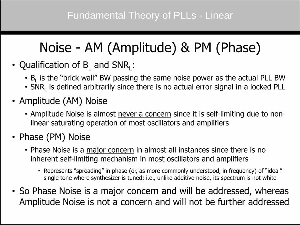
Noise - AM (Amplitude) & PM (Phase)
• Qualification of BL and SNRL:
• BL is the “brick-wall” BW passing the same noise power as the actual PLL BW • SNRL is defined arbitrarily since there is no actual error signal in a locked PLL
• Amplitude (AM) Noise
• Amplitude Noise is almost never a concern since it is self-limiting due to non-linear saturating operation of most oscillators and amplifiers
• Phase (PM) Noise
• Phase Noise is a major concern in almost all instances since there is no inherent self-limiting mechanism in most oscillators and amplifiers
• Represents “spreading” in phase (or, as more commonly understood, in frequency) of “ideal” single tone where synthesizer is tuned; i.e., unlike additive noise, its spectrum is not white
• So Phase Noise is a major concern and will be addressed, whereas Amplitude Noise is not a concern and will not be further addressed
Fundamental Theory of PLLs - Linear
Phase Noise Analysis - Domain Representations
• Time Domain • Representation - Signal Plus Noise: v(t) = [Vo+ am(t)]sin[wot + qm(t)]
• am(t) = Amplitude (AM) Noise - not a concern • qm(t) = Phase (PM) Noise - major concern (A.K.A. as “Jitter” in time domain) • Represented by Gaussian Distribution in Amplitude
• Frequency Domain • Lf(f) is single sideband (SSB) phase noise PSD normalized to carrier at
frequency offset, f, in units of rad2/Hz or dBc/Hz; i.e., modulated (RF) • Wf(f) is double sideband (DSB) phase noise PSD normalized to 1 rad2/Hz at
frequency offset, f, in units of rad2/Hz or dB/Hz; i.e., demodulated (baseband) • Approximate Relationship of Lf(f) to Wf(f):
• Linear: Wf(f) = 2Lf(f) • Logarithmic: 10 Log10 Wf(f) = 10 Log10 Lf(f) + 3 dB
• Can Convert Between Time and Frequency Domains • Possible using small-signal (linear) approximation for PM and FM
Fundamental Theory of PLLs - Linear
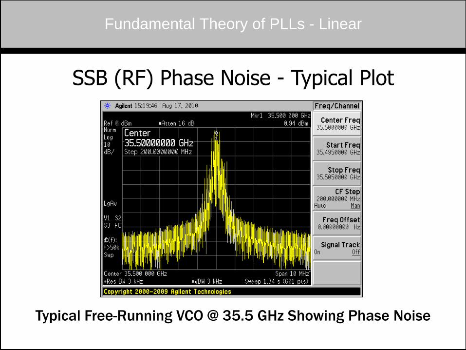
SSB (RF) Phase Noise - Typical Plot
Typical Free-Running VCO @ 35.5 GHz Showing Phase Noise
Fundamental Theory of PLLs - Linear
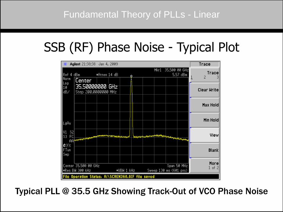
SSB (RF) Phase Noise - Typical Plot
Typical PLL @ 35.5 GHz Showing Track-Out of VCO Phase Noise
Fundamental Theory of PLLs - Linear
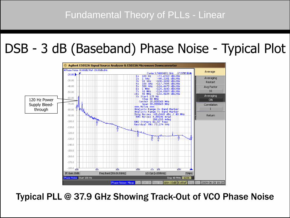
DSB - 3 dB (Baseband) Phase Noise - Typical Plot
Typical PLL @ 37.9 GHz Showing Track-Out of VCO Phase Noise
Fundamental Theory of PLLs - Linear
120 Hz Power Supply Bleed-
through
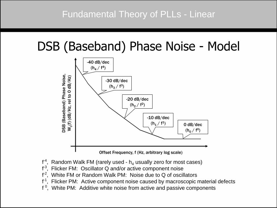
DSB (Baseband) Phase Noise - Model
Fundamental Theory of PLLs - Linear
f-4, Random Walk FM (rarely used - h4 usually zero for most cases)
f-3, Flicker FM: Oscillator Q and/or active component noise
f-2, White FM or Random Walk PM: Noise due to Q of oscillators
f-1, Flicker PM: Active component noise caused by macroscopic material defects
f 0, White PM: Additive white noise from active and passive components
Offset Frequency, f (Hz, arbitrary log scale)
DS
B (
Ba
se
ba
nd
) P
ha
se
No
ise
,
Wf(f
) (d
B/H
z, r
el to
0 d
B/H
z)
-40 dB/dec
(h4 / f4)
-20 dB/dec
(h2 / f2)
-30 dB/dec
(h3 / f3)
-10 dB/dec
(h1 / f1) 0 dB/dec
(h0 / f0)
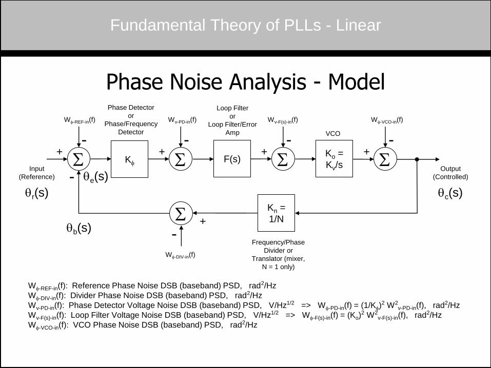
Phase Noise Analysis - Model
Ko =
Kv/s F(s)
Kn =
1/N
S
S
S S Input
(Reference)
Wf-REF-in(f)
Wf-DIV-in(f)
Wf-VCO-in(f) Wv-F(s)-in(f) Wv-PD-in(f)
Output
(Controlled)
Phase Detector
or
Phase/Frequency
Detector
Loop Filter
or
Loop Filter/Error
Amp
Frequency/Phase
Divider or
Translator (mixer,
N = 1 only)
VCO
-
-
+ + - -
+ + -
+
-
Fundamental Theory of PLLs - Linear
qb(s)
qe(s)
qc(s) qr(s)
Kf S
Wf-REF-in(f): Reference Phase Noise DSB (baseband) PSD, rad2/Hz
Wf-DIV-in(f): Divider Phase Noise DSB (baseband) PSD, rad2/Hz
Wv-PD-in(f): Phase Detector Voltage Noise DSB (baseband) PSD, V/Hz1/2 => Wf-PD-in(f) = (1/Kf)2 W2
v-PD-in(f), rad2/Hz
Wv-F(s)-in(f): Loop Filter Voltage Noise DSB (baseband) PSD, V/Hz1/2 => Wf-F(s)-in(f) = (Ko)2 W2
v-F(s)-in(f), rad2/Hz
Wf-VCO-in(f): VCO Phase Noise DSB (baseband) PSD, rad2/Hz
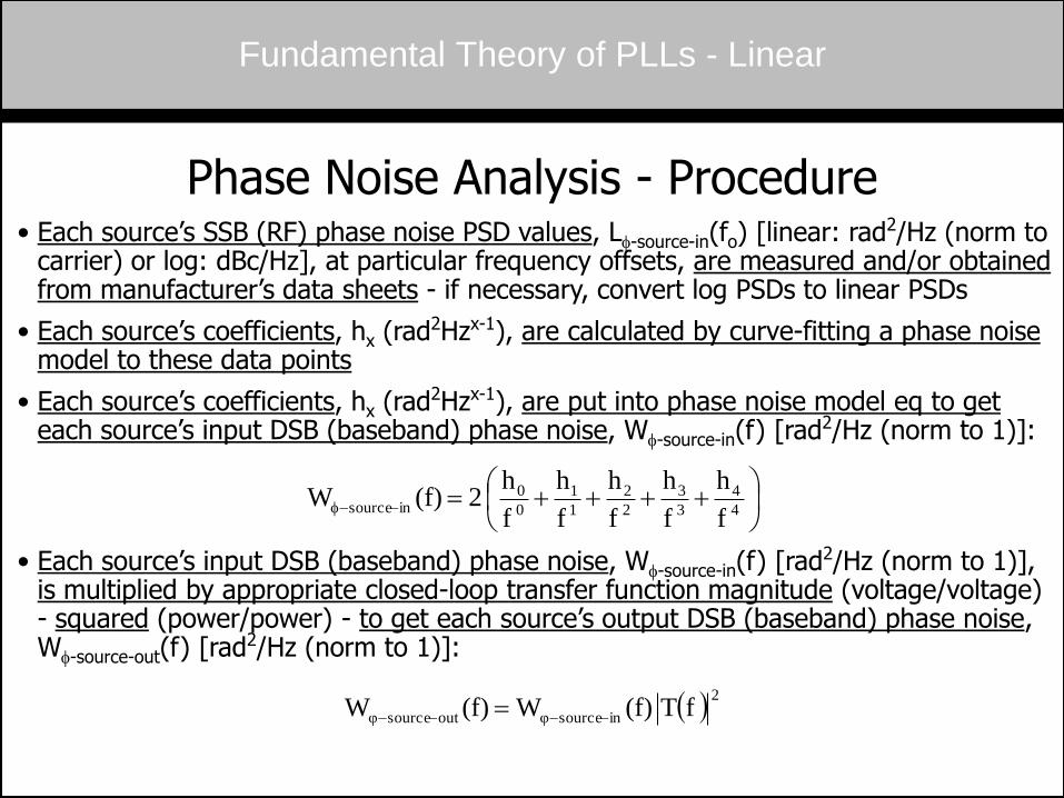
Phase Noise Analysis - Procedure
• Each source’s SSB (RF) phase noise PSD values, Lf-source-in(fo) [linear: rad2/Hz (norm to carrier) or log: dBc/Hz], at particular frequency offsets, are measured and/or obtained from manufacturer’s data sheets - if necessary, convert log PSDs to linear PSDs
• Each source’s coefficients, hx (rad2Hzx-1), are calculated by curve-fitting a phase noise model to these data points
• Each source’s coefficients, hx (rad2Hzx-1), are put into phase noise model eq to get each source’s input DSB (baseband) phase noise, Wf-source-in(f) [rad2/Hz (norm to 1)]:
• Each source’s input DSB (baseband) phase noise, Wf-source-in(f) [rad2/Hz (norm to 1)], is multiplied by appropriate closed-loop transfer function magnitude (voltage/voltage) - squared (power/power) - to get each source’s output DSB (baseband) phase noise, Wf-source-out(f) [rad2/Hz (norm to 1)]:
f 4
4
3
3
2
2
1
1
0
0insource
f
h
f
h
f
h
f
h
f
h 2(f)W
2
insourceφoutsourceφ fT (f)W(f)W
Fundamental Theory of PLLs - Linear
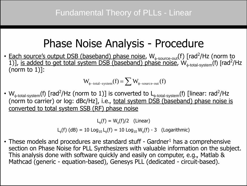
Phase Noise Analysis - Procedure
• Each source’s output DSB (baseband) phase noise, Wf-source-out(f) [rad2/Hz (norm to 1)], is added to get total system DSB (baseband) phase noise, Wf-total-system(f) [rad2/Hz (norm to 1)]:
• Wf-total-system(f) [rad2/Hz (norm to 1)] is converted to Lf-total-system(f) [linear: rad2/Hz
(norm to carrier) or log: dBc/Hz], i.e., total system DSB (baseband) phase noise is converted to total system SSB (RF) phase noise
Lf(f) = Wf(f)/2 (Linear)
Lf(f) (dB) = 10 Log10 Lf(f) = 10 Log10 Wf(f) - 3 (Logarithmic)
• These models and procedures are standard stuff - Gardner1 has a comprehensive section on Phase Noise for PLL Synthesizers with valuable information on the subject. This analysis done with software quickly and easily on computer, e.g., Matlab & Mathcad (generic - equation-based), Genesys PLL (dedicated - circuit-based).
ff (f)W(f)W outsourcesystemtotal
Fundamental Theory of PLLs - Linear
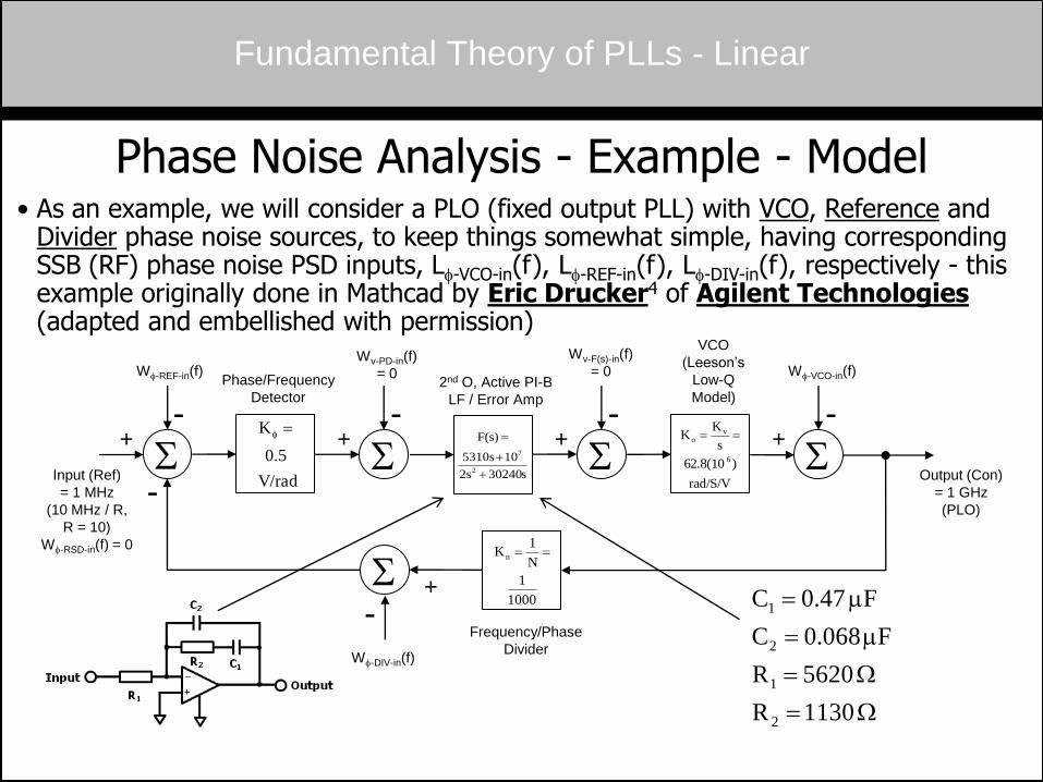
Fundamental Theory of PLLs - Linear
W
W
m
m
1130R
5620R
F 068.0C
F 47.0C
2
1
2
1
S
S
S S S Input (Ref)
= 1 MHz
(10 MHz / R,
R = 10)
Wf-RSD-in(f) = 0
Wf-REF-in(f)
Wf-DIV-in(f)
Wf-VCO-in(f)
Wv-F(s)-in(f)
= 0 Wv-PD-in(f)
= 0
Output (Con)
= 1 GHz
(PLO)
Phase/Frequency
Detector 2nd O, Active PI-B
LF / Error Amp
Frequency/Phase
Divider
VCO
(Leeson’s
Low-Q
Model)
-
-
+ + - -
+ + -
+
-
V/rad
5.0
K f
rad/S/V
)62.8(10
s
KK
6
vo
1000
1
N
1Kn
s302402s
105310s
F(s)
2
7
Phase Noise Analysis - Example - Model
• As an example, we will consider a PLO (fixed output PLL) with VCO, Reference and Divider phase noise sources, to keep things somewhat simple, having corresponding SSB (RF) phase noise PSD inputs, Lf-VCO-in(f), Lf-REF-in(f), Lf-DIV-in(f), respectively - this example originally done in Mathcad by Eric Drucker4 of Agilent Technologies (adapted and embellished with permission)
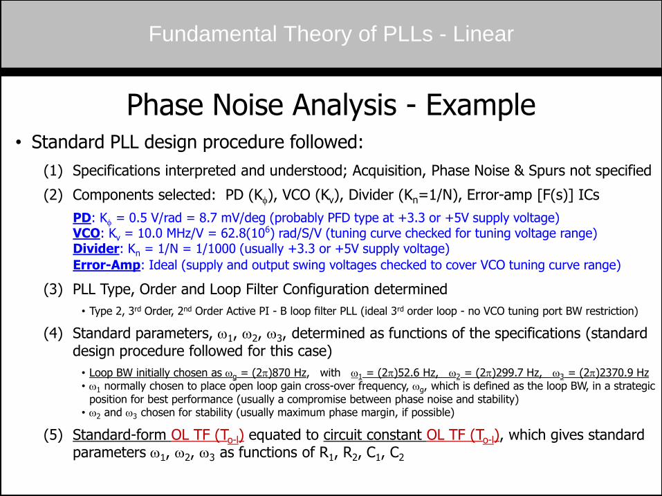
Fundamental Theory of PLLs - Linear
Phase Noise Analysis - Example
• Standard PLL design procedure followed:
(1) Specifications interpreted and understood; Acquisition, Phase Noise & Spurs not specified
(2) Components selected: PD (Kf), VCO (Kv), Divider (Kn=1/N), Error-amp [F(s)] ICs
PD: Kf = 0.5 V/rad = 8.7 mV/deg (probably PFD type at +3.3 or +5V supply voltage) VCO: Kv = 10.0 MHz/V = 62.8(106) rad/S/V (tuning curve checked for tuning voltage range) Divider: Kn = 1/N = 1/1000 (usually +3.3 or +5V supply voltage)
Error-Amp: Ideal (supply and output swing voltages checked to cover VCO tuning curve range)
(3) PLL Type, Order and Loop Filter Configuration determined
• Type 2, 3rd Order, 2nd Order Active PI - B loop filter PLL (ideal 3rd order loop - no VCO tuning port BW restriction)
(4) Standard parameters, w1, w2, w3, determined as functions of the specifications (standard design procedure followed for this case)
• Loop BW initially chosen as wg = (2p)870 Hz, with w1 = (2p)52.6 Hz, w2 = (2p)299.7 Hz, w3 = (2p)2370.9 Hz • w1 normally chosen to place open loop gain cross-over frequency, wg, which is defined as the loop BW, in a strategic
position for best performance (usually a compromise between phase noise and stability) • w2 and w3 chosen for stability (usually maximum phase margin, if possible)
(5) Standard-form OL TF (To-l) equated to circuit constant OL TF (To-l), which gives standard parameters w1, w2, w3 as functions of R1, R2, C1, C2
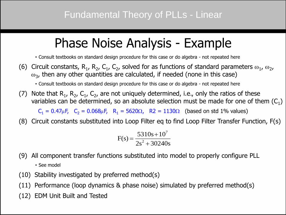
Fundamental Theory of PLLs - Linear
Phase Noise Analysis - Example
• Consult textbooks on standard design procedure for this case or do algebra - not repeated here
(6) Circuit constants, R1, R2, C1, C2, solved for as functions of standard parameters w1, w2, w3, then any other quantities are calculated, if needed (none in this case)
• Consult textbooks on standard design procedure for this case or do algebra - not repeated here
(7) Note that R1, R2, C1, C2, are not uniquely determined, i.e., only the ratios of these variables can be determined, so an absolute selection must be made for one of them (C1)
C1 = 0.47mF, C2 = 0.068mF, R1 = 5620W, R2 = 1130W (based on std 1% values)
(8) Circuit constants substituted into Loop Filter eq to find Loop Filter Transfer Function, F(s)
(9) All component transfer functions substituted into model to properly configure PLL
• See model
(10) Stability investigated by preferred method(s)
(11) Performance (loop dynamics & phase noise) simulated by preferred method(s)
(12) EDM Unit Built and Tested
30240s2s
105310sF(s)
2
7
(A) SSB Phase Noise Sources in PLL • VCO Phase Noise (Leeson’s Low-Q Model)
• SSB Phase Noise PSD values from measurements or data sheet:
• Floor: -155 dBc/Hz 10-15.5/Hz
• 10 KHz: -110 dBc/Hz 10-11/Hz
• 1/f (3-2) corner @ 5 KHz: -104 dBc/Hz 10-10.4/Hz
• Coefficients from curve-fitting model to PSD values:
h0/f0 = 10-15.5/Hz, h0 = (10-15.5/Hz)f0 = 10-15.5 rad2Hz-1
h1 = 0 rad2
h2/f2 = 10-11.0/Hz, h2 = (10-11/Hz)f2 = (10-11/Hz)(104)2 = 10-3 rad2Hz
h3/f3 = 10-10.4/Hz, h3 = (10-10.4/Hz)f3 = (10-10.4/Hz)[5(103)]3 = 100.7 rad2Hz2
h4 = 0 rad2Hz3
Fundamental Theory of PLLs - Linear
/Hzrad f
10
f
1010 2(f)W 2
3
0.7
2
-315.5-
inVCO
f
(PLOT) dBc/Hz 3(f)WLog 10(dB) (f)L inVCO10inVCO ff
(A) SSB Phase Noise Sources in PLL • Reference Phase Noise
• SSB Phase Noise PSD values from measurements or data sheet:
• Floor: -158 dBc/Hz 10-15.8/Hz
• 1250 Hz: -158 dBc/Hz 10-15.8/Hz
• 625 Hz: -155 dBc/Hz 10-15.5/Hz
• 1/f (3-2) corner @ 125 Hz: -141 dBc/Hz 10-14.1/Hz
• Coefficients from curve-fitting model to PSD values:
h0/f0 = 10-15.8/Hz, h0 = (10-15.8/Hz)f0 = 10-15.8 rad2Hz-1
h1/f1 = 10-15.8/Hz, h1 = (10-15.8/Hz)f1 = (10-15.8/Hz)(1250)1 = 10-12.7 rad2
h2/f2 = 10-15.5/Hz, h2 = (10-15.5/Hz)f2 = (10-15.5/Hz)(625)2 = 10-9.9 rad2Hz
h3/f3 = 10-14.1/Hz, h3 = (10-14.1/Hz)f3 = (10-14.1/Hz)(125)3 = 10-7.8 rad2Hz2
h4 = 0 rad2Hz3
Fundamental Theory of PLLs - Linear
/Hzrad f
10
f
10
f
1010 2(f)W 2
3
-7.8
2
-9.9-12.715.8-
inRef
f
(PLOT) dBc/Hz 3(f)WLog 10(dB) (f)L inRef10inRef ff
(A) SSB Phase Noise Sources in PLL • Divider Phase Noise
• SSB Phase Noise PSD values from measurements or data sheet:
• Floor: -155 dBc/Hz 10-15.5/Hz
• 1/f (1-0) corner @ 1 KHz: -155 dBc/Hz 10-15.5/Hz
• Coefficients from curve-fitting model to PSD values:
h0/f0 = 10-15.5/Hz, h0 = (10-15.5/Hz)f0 = 10-15.5 rad2Hz-1
h1/f1 = 10-15.5/Hz, h1 = (10-15.5/Hz)f1 = (10-15.5/Hz)(103)1 = 10-12.5 rad2
h2 = 0 rad2Hz
h3 = 0 rad2Hz2
h4 = 0 rad2Hz3
Fundamental Theory of PLLs - Linear
/Hzrad f
1010 2(f)W 2
-12.515.5-
inDiv
f
(PLOT) dBc/Hz 3(f)WLog 10(dB) (f)L inDiv10inDiv ff
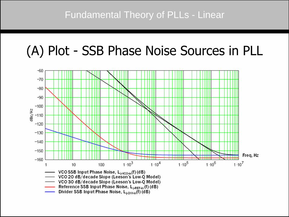
(A) Plot - SSB Phase Noise Sources in PLL
Fundamental Theory of PLLs - Linear
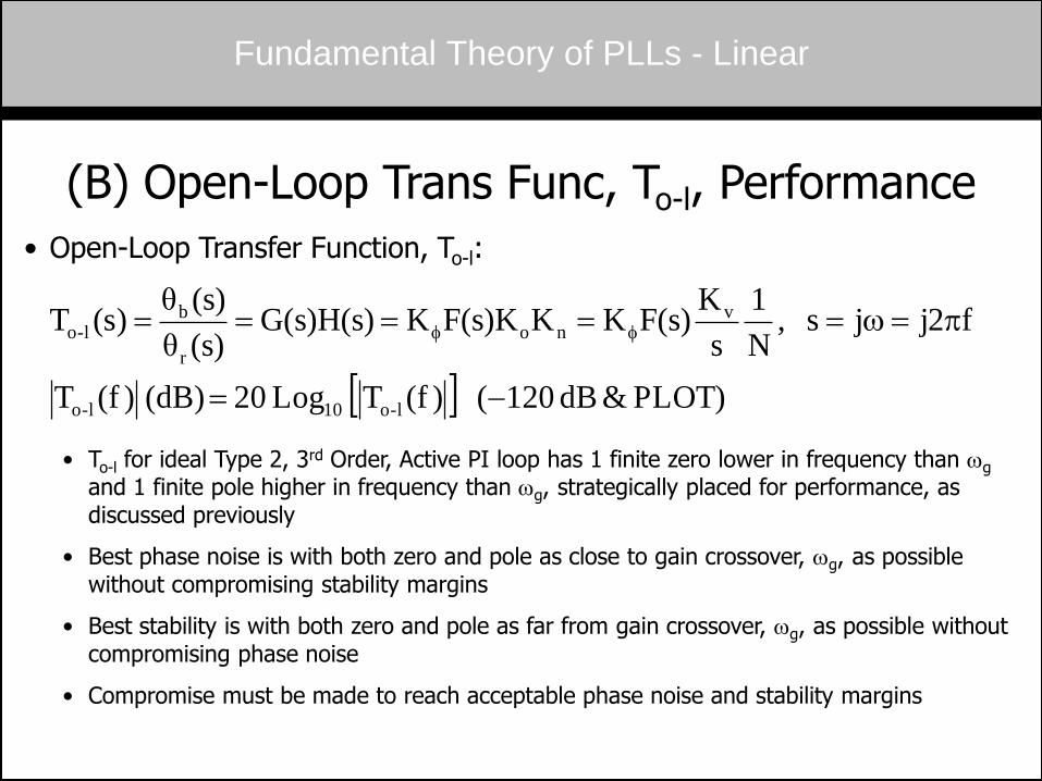
Fundamental Theory of PLLs - Linear
(B) Open-Loop Trans Func, To-l, Performance
• Open-Loop Transfer Function, To-l:
• To-l for ideal Type 2, 3rd Order, Active PI loop has 1 finite zero lower in frequency than wg and 1 finite pole higher in frequency than wg, strategically placed for performance, as discussed previously
• Best phase noise is with both zero and pole as close to gain crossover, wg, as possible without compromising stability margins
• Best stability is with both zero and pole as far from gain crossover, wg, as possible without compromising phase noise
• Compromise must be made to reach acceptable phase noise and stability margins
PLOT) & dB 120( )f(T Log 20 (dB) )f(T
f2jjs ,N
1
s
KF(s)KKF(s)KKG(s)H(s)
(s)θ
(s)θ)s(T
l-o10l-o
vno
r
bl-o
pw ff
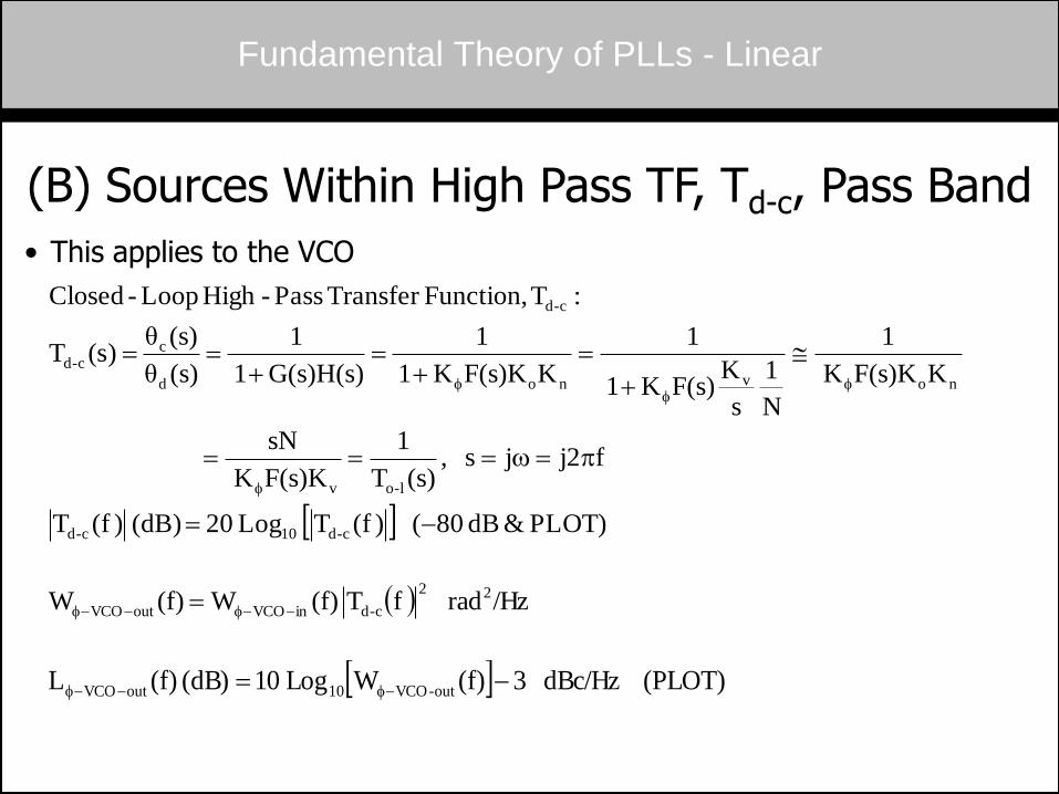
Fundamental Theory of PLLs - Linear
(B) Sources Within High Pass TF, Td-c, Pass Band
• This applies to the VCO
/Hzrad fT (f)W(f)W 22
c-dinVCOoutVCO ff
PLOT) & dB 80( )f(T Log 20 (dB) )f(T
fj2js ,(s)T
1
F(s)KK
sN
KF(s)KK
1
N
1
s
KF(s)K1
1
KF(s)KK1
1
G(s)H(s)1
1
(s)θ
(s)θ )s(T
:T Function,Transfer Pass-High Loop-Closed
c-d10c-d
l-ov
novnod
cc-d
c-d
pw
f
ff
f
(PLOT) dBc/Hz 3(f)WLog 10(dB) (f)L out-VCO10outVCO ff
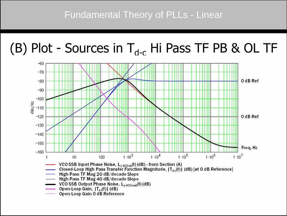
(B) Plot - Sources in Td-c Hi Pass TF PB & OL TF
Fundamental Theory of PLLs - Linear
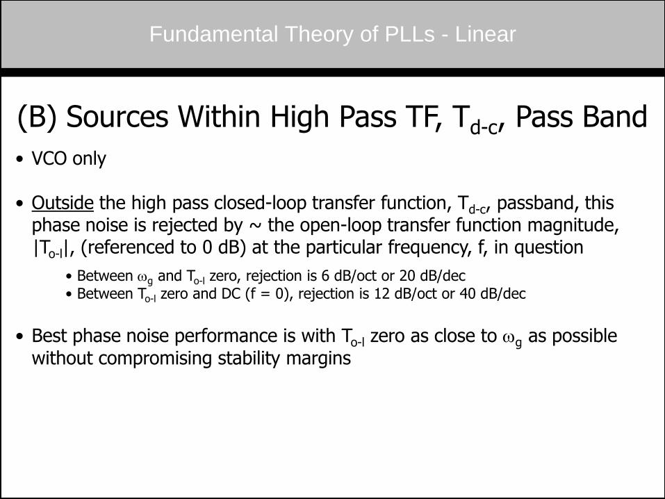
(B) Sources Within High Pass TF, Td-c, Pass Band
• VCO only • Outside the high pass closed-loop transfer function, Td-c, passband, this
phase noise is rejected by ~ the open-loop transfer function magnitude, |To-l|, (referenced to 0 dB) at the particular frequency, f, in question
• Between wg and To-l zero, rejection is 6 dB/oct or 20 dB/dec • Between To-l zero and DC (f = 0), rejection is 12 dB/oct or 40 dB/dec
• Best phase noise performance is with To-l zero as close to wg as possible
without compromising stability margins
Fundamental Theory of PLLs - Linear
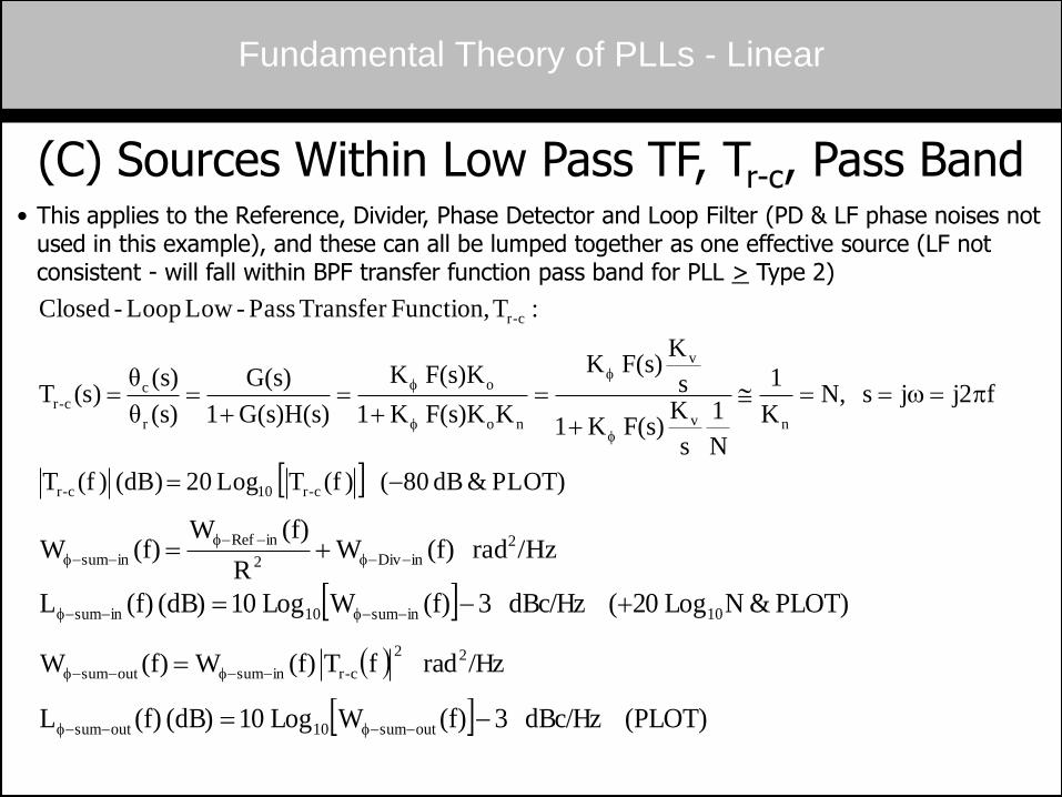
Fundamental Theory of PLLs - Linear
(C) Sources Within Low Pass TF, Tr-c, Pass Band
• This applies to the Reference, Divider, Phase Detector and Loop Filter (PD & LF phase noises not used in this example), and these can all be lumped together as one effective source (LF not consistent - will fall within BPF transfer function pass band for PLL > Type 2)
PLOT) & dB 80( )f(T Log 20 (dB) )f(T
fj2js N,K
1
N
1
s
KF(s) K1
s
KF(s) K
KF(s)K K1
F(s)K K
G(s)H(s)1
G(s)
(s)θ
(s)θ)s(T
:T Function,Transfer Pass-Low Loop-Closed
c-r10c-r
nv
v
no
o
r
cc-r
c-r
pw
f
f
f
f
/Hzrad fT (f)W(f)W 22
c-rinsumoutsum ff
(PLOT) dBc/Hz 3(f)WLog 10(dB) (f)L outsum10outsum ff
/Hzrad (f)W R
(f)W(f)W 2
inDiv2
inRef
insum f
f
f
PLOT) & NLog 20( dBc/Hz 3(f)WLog 10(dB) (f)L 10insum10insum ff
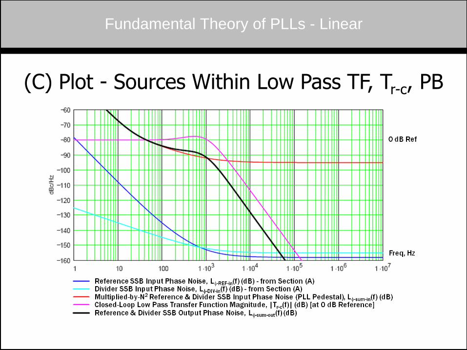
(C) Plot - Sources Within Low Pass TF, Tr-c, PB
Fundamental Theory of PLLs - Linear
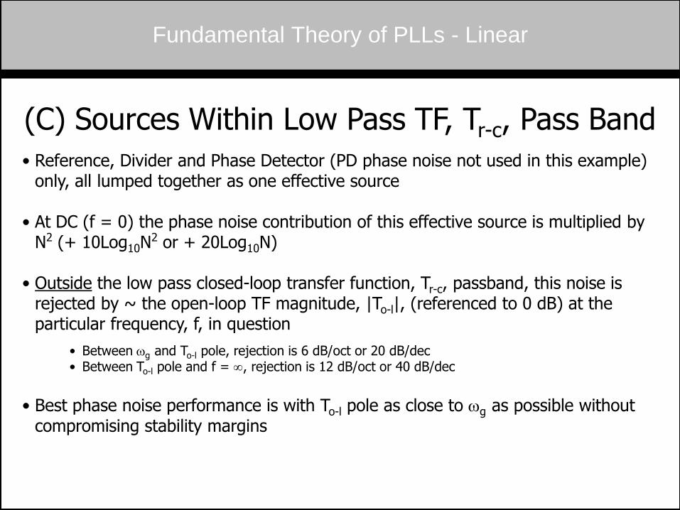
(C) Sources Within Low Pass TF, Tr-c, Pass Band
• Reference, Divider and Phase Detector (PD phase noise not used in this example) only, all lumped together as one effective source
• At DC (f = 0) the phase noise contribution of this effective source is multiplied by
N2 (+ 10Log10N2 or + 20Log10N)
• Outside the low pass closed-loop transfer function, Tr-c, passband, this noise is
rejected by ~ the open-loop TF magnitude, |To-l|, (referenced to 0 dB) at the particular frequency, f, in question
• Between wg and To-l pole, rejection is 6 dB/oct or 20 dB/dec • Between To-l pole and f = , rejection is 12 dB/oct or 40 dB/dec
• Best phase noise performance is with To-l pole as close to wg as possible without
compromising stability margins
Fundamental Theory of PLLs - Linear
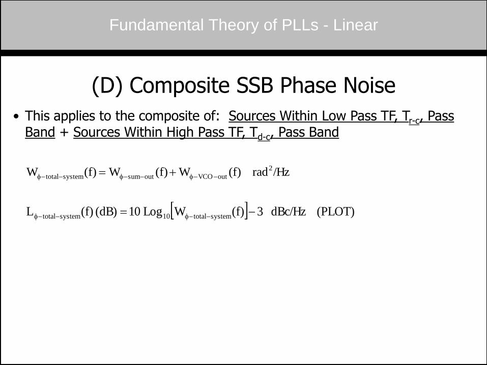
(D) Composite SSB Phase Noise
• This applies to the composite of: Sources Within Low Pass TF, Tr-c, Pass Band + Sources Within High Pass TF, Td-c, Pass Band
Fundamental Theory of PLLs - Linear
/Hzrad (f)W(f)W(f)W 2
outVCOoutsumsystemtotal fff
(PLOT) dBc/Hz 3(f)WLog 10(dB) (f)L systemtotal10systemtotal ff
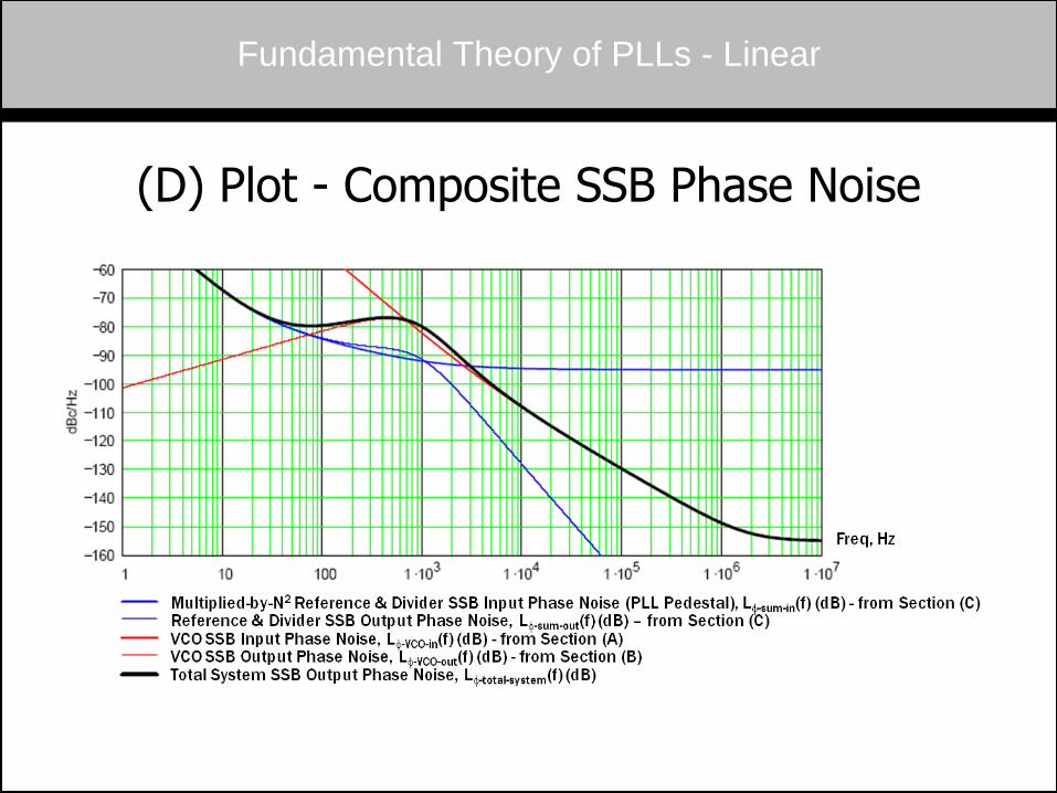
(D) Plot - Composite SSB Phase Noise
Fundamental Theory of PLLs - Linear
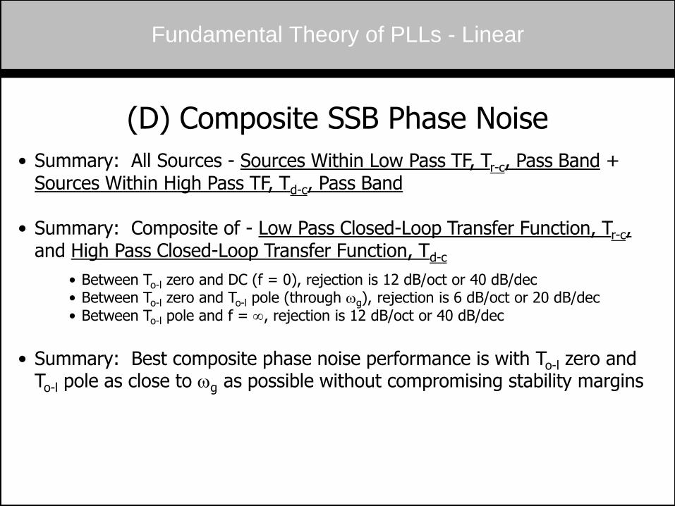
(D) Composite SSB Phase Noise
• Summary: All Sources - Sources Within Low Pass TF, Tr-c, Pass Band + Sources Within High Pass TF, Td-c, Pass Band
• Summary: Composite of - Low Pass Closed-Loop Transfer Function, Tr-c,
and High Pass Closed-Loop Transfer Function, Td-c
• Between To-l zero and DC (f = 0), rejection is 12 dB/oct or 40 dB/dec • Between To-l zero and To-l pole (through wg), rejection is 6 dB/oct or 20 dB/dec • Between To-l pole and f = , rejection is 12 dB/oct or 40 dB/dec
• Summary: Best composite phase noise performance is with To-l zero and
To-l pole as close to wg as possible without compromising stability margins
Fundamental Theory of PLLs - Linear
Fundamental Theory of PLLs - Linear
(E) Methods to Produce Opt SSB Phase Noise
• If Reference and VCO phase noise dominate other sources, choose loop BW at Intersection of “sources within low pass TF, Tr-c, phase noise multiplied-by-N2” (PLL Pedestal) and “sources within high pass TF, Td-c, phase noise” (VCO) Curves
• PLO re-specified for loop BW, wg, to produce optimum phase noise (see previous Pedestal & VCO phase noise source curves or mathematically calculate from intersection of these curves)
• This gives: wg = 2.5 KHz • Same components retained, only standard parameters changed to meet optimum
specification, then standard design procedure repeated, phase noise analysis done, and phase noise plotted
Fundamental Theory of PLLs - Linear
(E) Methods to Produce Opt SSB Phase Noise
• Keep N (Kn) as small (large) as possible, with “1” being the ultimate goal (possibly by increasing Reference frequency and decreasing Divider ratio by same factor)
• PLO re-specified for loop BW, wg, to produce improved optimum phase noise (plot new Pedestal & VCO source curves or mathematically calculate from intersection of these curves) using 10 MHz Reference (frequency increased by factor dR = 10: from 1 MHz to 10 MHz) with factor dR
2 = 100 (20 dB) higher phase noise, and 1/100 Divider (ratio decreased by factor dN = 10: from 1/1000 to 1/100) with factor dN = 10 (10 dB) higher phase noise, producing lower composite SSB phase noise
• This gives: wg = 6.6 KHz • Same components retained, only standard parameters changed to meet improved
optimum spec, then standard design procedure repeated, phase noise analysis done, and phase noise plotted
• Analysis: According to Eric Drucker of Agilent Technologies, the Divider phase noise does not increase by a factor of dN = 10 (10 dB); the PD phase noise increases by this amount (at least for PFDs), but our model does not include PD phase noise, so we assign this increase to the Divider for analysis purposes, since it is processed in the same way
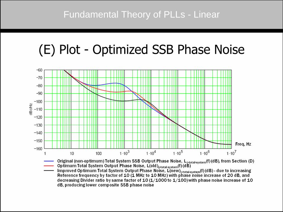
(E) Plot - Optimized SSB Phase Noise
Fundamental Theory of PLLs - Linear
(E) Methods to Produce Opt SSB Phase Noise
• Obviously choose lowest noise PLL components without compromising other performance characteristics
• Choose a translational feedback loop topology, which maintains Kn = N = 1
• Means using mixer(s) instead of divider(s) as feedback converter
• Mixer feedback usually more difficult to implement from technical, SWAP & Cost considerations
• Tunable LO for mixer FB can be obtained from direct synthesis (giving best phase noise) or another PLL (giving worse phase noise over direct approach)
• Done in practice with good results
• Keep noise “Pollution” (i.e., voltage noise) from resistors in PLL circuit to a minimum by using smallest possible values of resistors [thereby lowering thermal (kTB) voltage noise] in circuit without compromising system or component operation and performance
Fundamental Theory of PLLs - Linear
Spurious - Types of Spurious in PLLs
• Modulation Effects (of VCO, active loop filter, PD, divider) - usually Symmetric
• Power and control line noise • Reference and harmonics thereof getting on VCO control line • Reference source modulation
• Mixing Products - usually Asymmetric
• Loops using Translational (mixer) FB rather than Divider FB
• VCO Subharmonics - usually Asymmetric
• Loops using non-fundamental frequency VCOs
• Digital Systems, Circuits and Clocks - can be symmetric or asymmetric
• Susceptibility (Coupling) Methods
• Conducted or Radiated from physically adjacent analog or digital circuit subsections
Fundamental Theory of PLLs - Linear
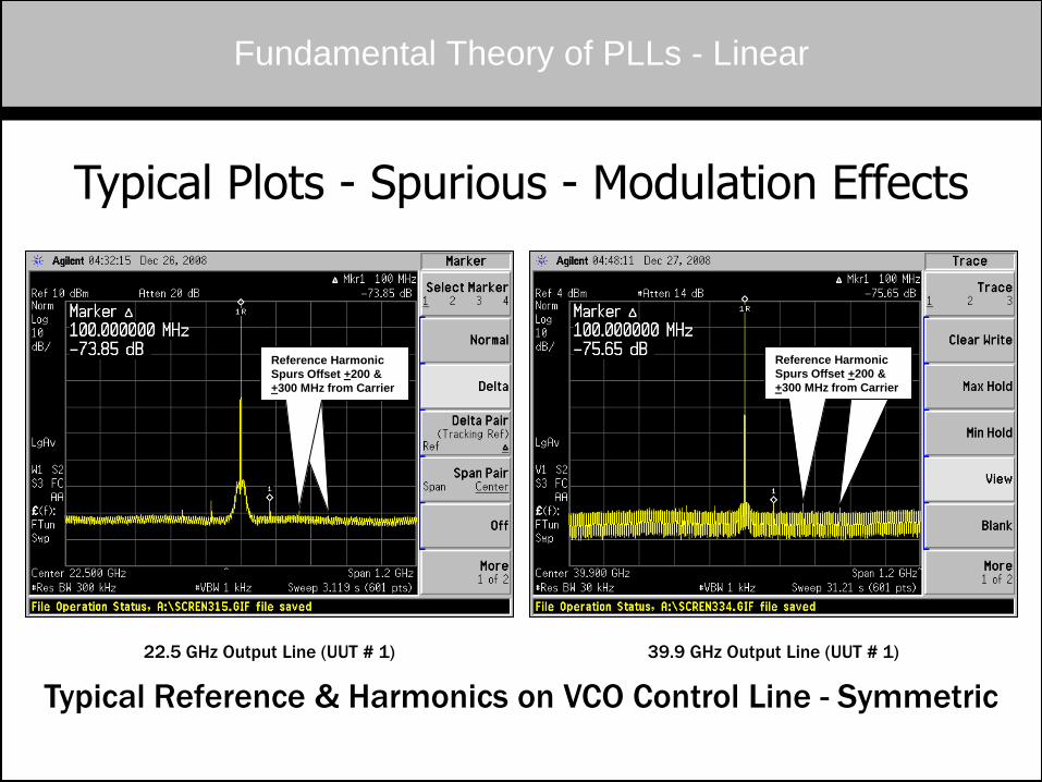
Typical Plots - Spurious - Modulation Effects
Typical Reference & Harmonics on VCO Control Line - Symmetric
Reference Harmonic
Spurs Offset +200 &
+300 MHz from Carrier
Reference Harmonic
Spurs Offset +200 &
+300 MHz from Carrier
22.5 GHz Output Line (UUT # 1) 39.9 GHz Output Line (UUT # 1)
Fundamental Theory of PLLs - Linear
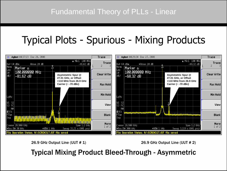
Typical Plots - Spurious - Mixing Products
Typical Mixing Product Bleed-Through - Asymmetric
Asymmetric Spur @
27.01 GHz, or Offset
+110 MHz from 26.9 GHz
Carrier (~ -70 dBc)
Asymmetric Spur @
27.01 GHz, or Offset
+110 MHz from 26.9 GHz
Carrier (~ -70 dBc)
26.9 GHz Output Line (UUT # 1) 26.9 GHz Output Line (UUT # 2)
Fundamental Theory of PLLs - Linear
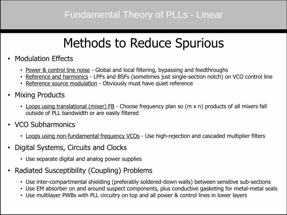
Methods to Reduce Spurious
• Modulation Effects
• Power & control line noise - Global and local filtering, bypassing and feedthroughs • Reference and harmonics - LPFs and BSFs (sometimes just single-section notch) on VCO control line • Reference source modulation - Obviously must have quiet reference
• Mixing Products
• Loops using translational (mixer) FB - Choose frequency plan so (m x n) products of all mixers fall outside of PLL bandwidth or are easily filtered
• VCO Subharmonics
• Loops using non-fundamental frequency VCOs - Use high-rejection and cascaded multiplier filters
• Digital Systems, Circuits and Clocks
• Use separate digital and analog power supplies
• Radiated Susceptibility (Coupling) Problems
• Use inter-compartmental shielding (preferably soldered-down walls) between sensitive sub-sections • Use EM absorber on and around suspect components, plus conductive gasketing for metal-metal seals • Use multilayer PWBs with PLL circuitry on top and all power & control lines in lower layers
Fundamental Theory of PLLs - Linear

Acquisition and Tracking
• General
• Acquisition
• Questions: (1) How can a PLL attain lock? (2) How long will it take to attain lock?
• Tracking
• Qualification: Non-linear - just before PLL breaks lock; linear discussed previously
• Question: (1) Under what conditions, static or dynamic, will a PLL break lock?
• Acquisition
• Fact: A “Type N” loop has “N” forms of acquisition
• Definitions
• Phase Acquisition: Acquisition of phase (offset), by the phase detector, without encountering cycle slips (normally referred to as “acquisition”); self-acquisition of phase is A.K.A. Lock-In, with associated Lock-In Range and Lock-In Time
Fundamental Theory of PLLs - Non-Linear
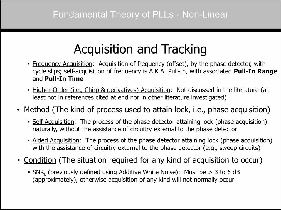
Acquisition and Tracking
• Frequency Acquisition: Acquisition of frequency (offset), by the phase detector, with cycle slips; self-acquisition of frequency is A.K.A. Pull-In, with associated Pull-In Range and Pull-In Time
• Higher-Order (i.e., Chirp & derivatives) Acquisition: Not discussed in the literature (at least not in references cited at end nor in other literature investigated)
• Method (The kind of process used to attain lock, i.e., phase acquisition)
• Self Acquisition: The process of the phase detector attaining lock (phase acquisition) naturally, without the assistance of circuitry external to the phase detector
• Aided Acquisition: The process of the phase detector attaining lock (phase acquisition) with the assistance of circuitry external to the phase detector (e.g., sweep circuits)
• Condition (The situation required for any kind of acquisition to occur)
• SNRL (previously defined using Additive White Noise): Must be > 3 to 6 dB (approximately), otherwise acquisition of any kind will not normally occur
Fundamental Theory of PLLs - Non-Linear
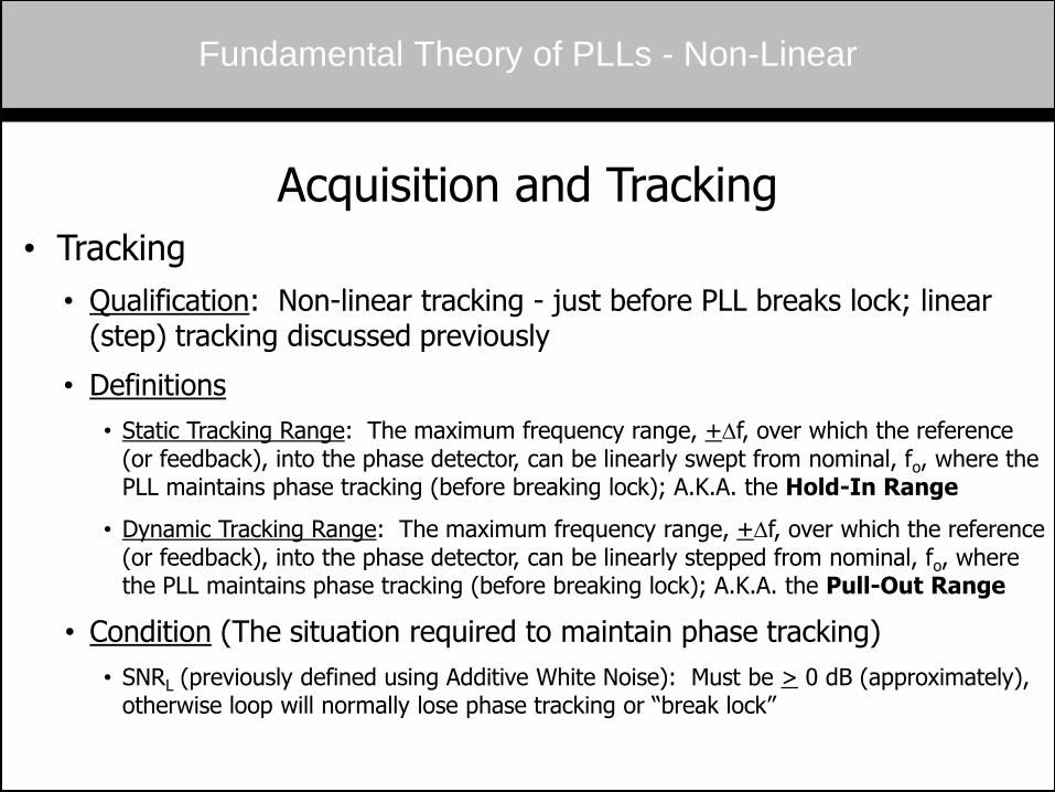
Fundamental Theory of PLLs - Non-Linear
Acquisition and Tracking
• Tracking
• Qualification: Non-linear tracking - just before PLL breaks lock; linear (step) tracking discussed previously
• Definitions
• Static Tracking Range: The maximum frequency range, +Df, over which the reference (or feedback), into the phase detector, can be linearly swept from nominal, fo, where the PLL maintains phase tracking (before breaking lock); A.K.A. the Hold-In Range
• Dynamic Tracking Range: The maximum frequency range, +Df, over which the reference (or feedback), into the phase detector, can be linearly stepped from nominal, fo, where the PLL maintains phase tracking (before breaking lock); A.K.A. the Pull-Out Range
• Condition (The situation required to maintain phase tracking)
• SNRL (previously defined using Additive White Noise): Must be > 0 dB (approximately), otherwise loop will normally lose phase tracking or “break lock”
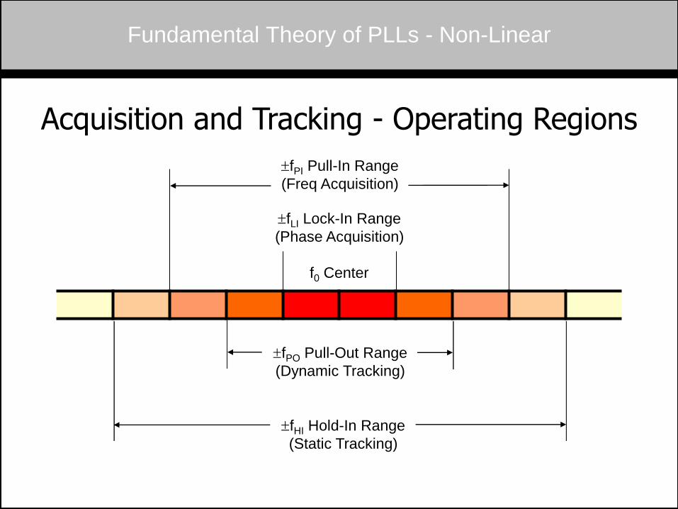
Acquisition and Tracking - Operating Regions
Fundamental Theory of PLLs - Non-Linear
fLI Lock-In Range
(Phase Acquisition)
fPI Pull-In Range
(Freq Acquisition)
f0 Center
fPO Pull-Out Range
(Dynamic Tracking)
fHI Hold-In Range
(Static Tracking)
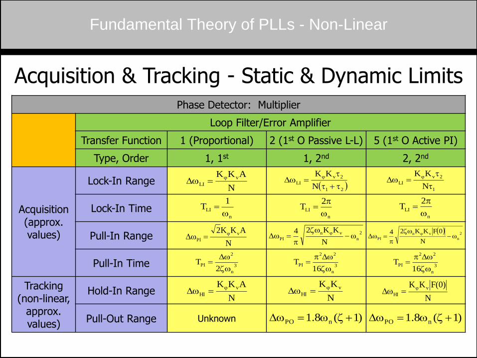
Fundamental Theory of PLLs - Non-Linear
Acquisition & Tracking - Static & Dynamic Limits Phase Detector: Multiplier
Loop Filter/Error Amplifier
Transfer Function 1 (Proportional) 2 (1st O Passive L-L) 5 (1st O Active PI)
Type, Order 1, 1st 1, 2nd 2, 2nd
Acquisition (approx. values)
Lock-In Range
Lock-In Time
Pull-In Range
Pull-In Time
Tracking (non-linear,
approx. values)
Hold-In Range
Pull-Out Range Unknown
n
LI
2T
w
p
2
n
vn
PI ωN
KK24ω
zw
pD
3
n
22
PI16
Tzw
wDp
N
KK v
HI
wD
)1(8.1 nPO zwwD
n
LI
2T
w
p
3
n
22
PI16
Tzw
wDp
N
)0(FKK v
HI
wD
)1(8.1 nPO zwwD
N
AKK v
LI
wD
N
AKK v
HI
wD
n
LI
1T
w
3
n
2
PI2
Tzw
wD
2
n
vn
PI ωN
0FKK24ω
zw
pD
21
2v
LIN
KK
wD
1
2v
LIN
KK
wD
N
AKK2ω
v
PI
D
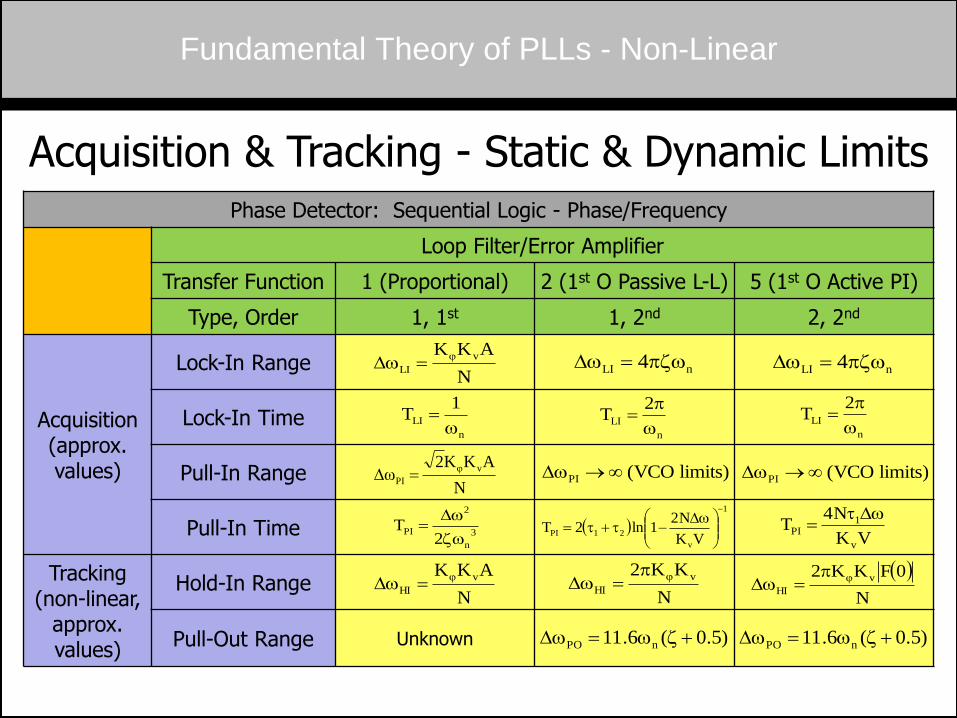
Fundamental Theory of PLLs - Non-Linear
Phase Detector: Sequential Logic - Phase/Frequency
Loop Filter/Error Amplifier
Transfer Function 1 (Proportional) 2 (1st O Passive L-L) 5 (1st O Active PI)
Type, Order 1, 1st 1, 2nd 2, 2nd
Acquisition (approx. values)
Lock-In Range
Lock-In Time
Pull-In Range
Pull-In Time
Tracking (non-linear,
approx. values)
Hold-In Range
Pull-Out Range Unknown
Acquisition & Tracking - Static & Dynamic Limits
nLI 4pzwwD nLI 4pzwwD
n
LI
2T
w
p
limits) (VCO PI wD limits) (VCO PI wD
)5.0(6.11 nPO zwwD )5.0(6.11 nPO zwwD
1
v
21PIVK
N21ln2T
wD
VK
N4T
v
1PI
wD
n
LI
2T
w
p
N
KK2 v
HI
pwD
N
0FKK2 v
HI
pwD
N
AKK2ω
v
PI
D
3
n
2
PI2
Tzw
wD
N
AKK v
HI
wD
N
AKK v
LI
wD
n
LI
1T
w
Fundamental Theory of PLLs - Non-Linear
Acquisition & Tracking - Static & Dynamic Limits
• Variable (Less Common) Definitions in Tables
• A: Gain of Proportional loop filter (from loop filter table)
• 1: Loop Filter Time Constant, R1C1, in 1st Order Passive Lead-Lag & 1st Order Active PI loop filters [# (2) & (5) from loop filter table]
• 2: Loop Filter Time Constant, R2C1, in 1st Order Passive Lead-Lag & 1st Order Active PI loop filters [# (2) & (5) from loop filter table]
• |F(0)|: Gain at s=w=f=0 of 1st Order Active PI loop filter
• Dw: Initial frequency difference between reference and feedback in PD
• V: PD power supply voltage (positive-to-negative)
• References for these formulas and values (in order of relevance):
• Best2, Brennan3, Gardner1
Fundamental Theory of PLLs - Non-Linear
Acquisition & Tracking - Static & Dynamic Limits
• Limits for our “Simple Example Synthesizer”, done previously, using Multiplier type PD (smaller BWs compared to PFD type PD - cannot use in this case due to inadequate pull-out range; see below)
• 6 MHz Output (larger Tr-c, smaller To-l narrower BWs, longer Ts; than 4 MHz):
• Lock-In Range, DfLI = 1337.8 Hz (must be < operating BW of PD) • Lock-In Time, TLI = 1.044 mS (requirement is 2 mS, stepped 4 - 6 MHz) • Pull-In Range, DfPI = 1,014,830.9 Hz • Pull-In Time, TPI = 1.6(10-7)(Df)2 mS (e.g., Df = 10,000 Hz, TPI = 16.0 mS) • Hold-In Range, DfHI = 3.316(108) Hz (assuming |F(0)| ~ 100,000 or 100 dB)
• Pull-Out Range, DfPO = 2928.0 Hz (need > 8333 Hz range, cannot use multiplier PD in this case)
• 4 MHz Output (smaller Tr-c, larger To-l wider BWs, shorter Ts; than 6 MHz):
• Lock-In Range, DfLI = 2006.7 Hz (must be < operating BW of PD) • Lock-In Time, TLI = 0.852 mS (6 - 4 MHz step should be < 4 - 6 MHz step of 2 mS) • Pull-In Range, DfPI = 1,375,534.6 Hz • Pull-In Time, TPI = 7.1(10-8)(Df)2 mS (e.g., Df = 10,000 Hz, TPI = 7.1 mS) • Hold-In Range, DfHI = 4.974(108) Hz (assuming |F(0)| ~ 100,000 or 100 dB)
• Pull-Out Range, DfPO = 3917.8 Hz (need > 12500 Hz range, cannot use multiplier PD in this case)
Fundamental Theory of PLLs - Non-Linear
Acquisition & Tracking - Static & Dynamic Limits
• Limits for our “Simple Example Synthesizer”, done previously, using PFD type PD (larger BWs compared to Multiplier type PD - can use in this case due to adequate pull-out range; see below)
• 6 MHz Output (larger Tr-c, smaller To-l narrower BWs, longer Ts; than 4 MHz):
• Lock-In Range, DfLI = 8402.8 Hz (must be < operating BW of PD, which is likely in this case) • Lock-In Time, TLI = 1.044 mS (requirement is 2 mS, stepped 4 - 6 MHz) • Pull-In Range, DfPI Hz (VCO limits) • Pull-In Time, TPI = 8.7(10-5)Df/V mS (e.g., Df = 100 KHz, V = 5 Volts, TPI = 1.7 mS) • Hold-In Range, DfHI = 2.083(109) Hz (assuming |F(0)| ~ 100,000 or 100 dB)
• Pull-Out Range, DfPO = 13312.9 Hz (need > 8333 Hz range, can use PFD type PD in this case)
• 4 MHz Output (smaller Tr-c, larger To-l wider BWs, shorter Ts; than 6 MHz):
• Lock-In Range, DfLI = 12606.6 Hz (must be < operating BW of PD, which is likely in this case) • Lock-In Time, TLI = 0.852 mS (6 - 4 MHz step should be < 4 - 6 MHz step of 2 mS) • Pull-In Range, DfPI Hz (VCO limits) • Pull-In Time, TPI = 5.8(10-5)Df/V mS (e.g., Df = 100 KHz, V = 5 Volts, TPI = 1.2 mS) • Hold-In Range, DfHI = 3.125(109) Hz (assuming |F(0)| ~ 100,000 or 100 dB)
• Pull-Out Range, DfPO = 18442.5 Hz (need > 12500 Hz range, can use PFD type PD in this case)
PLL Components
Phase Detectors (Phase Comparators)
• Operation: Develops Average (DC) output signal proportional to phase difference between 2 AC input signals
• Important Parameter for PLLs (contained in s-curve of PD)
• Transfer function (Gain), DVf = KfDf, Kf has units of V/rad, hopefully is linear (i.e., Kf is constant)
• Can vary with reference and feedback operating frequencies within PD operating bandwidth
• Other Important Concerns
• Operating BW
• Phase Noise (normally floor, or f0, with slight close-in flicker, or f-1, profile)
• Multiplier (Combinational) Type
• Operation: Develops average (DC) output component proportional to phase difference between 2 AC input signals by forming the product of the 2 signals, which, through
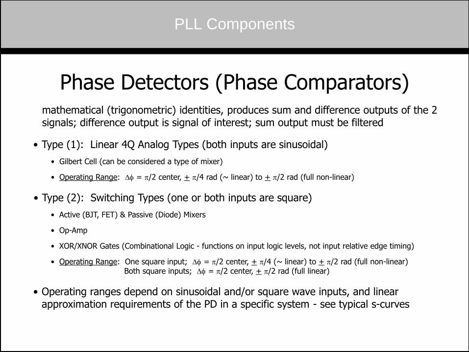
PLL Components
Phase Detectors (Phase Comparators)
mathematical (trigonometric) identities, produces sum and difference outputs of the 2 signals; difference output is signal of interest; sum output must be filtered
• Type (1): Linear 4Q Analog Types (both inputs are sinusoidal)
• Gilbert Cell (can be considered a type of mixer)
• Operating Range: Df = p/2 center, + p/4 rad (~ linear) to + p/2 rad (full non-linear)
• Type (2): Switching Types (one or both inputs are square)
• Active (BJT, FET) & Passive (Diode) Mixers
• Op-Amp
• XOR/XNOR Gates (Combinational Logic - functions on input logic levels, not input relative edge timing)
• Operating Range: One square input; Df = p/2 center, + p/4 (~ linear) to + p/2 rad (full non-linear) Both square inputs; Df = p/2 center, + p/2 rad (full linear)
• Operating ranges depend on sinusoidal and/or square wave inputs, and linear approximation requirements of the PD in a specific system - see typical s-curves
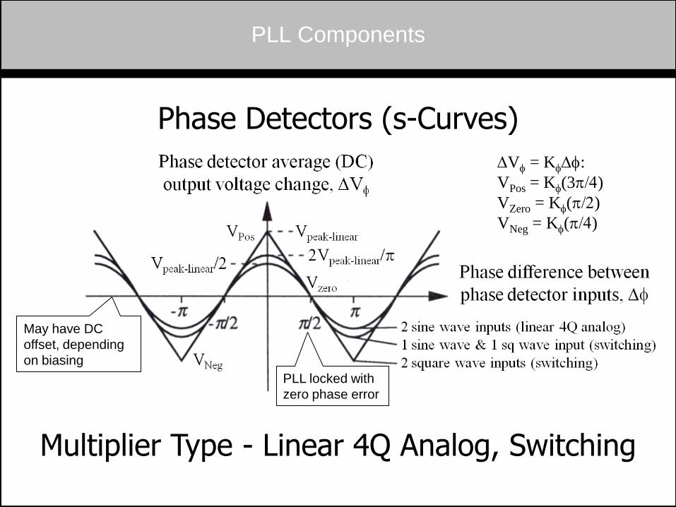
PLL Components
Phase Detectors (s-Curves)
Multiplier Type - Linear 4Q Analog, Switching
DVf = KfDf:
VPos = Kf(3p/4)
VZero = Kf(p/2)
VNeg = Kf(p/4)
PLL locked with
zero phase error
May have DC
offset, depending
on biasing
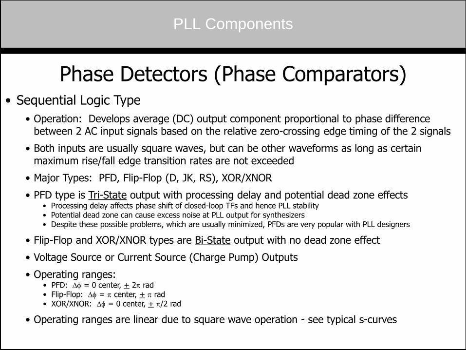
PLL Components
Phase Detectors (Phase Comparators)
• Sequential Logic Type
• Operation: Develops average (DC) output component proportional to phase difference between 2 AC input signals based on the relative zero-crossing edge timing of the 2 signals
• Both inputs are usually square waves, but can be other waveforms as long as certain maximum rise/fall edge transition rates are not exceeded
• Major Types: PFD, Flip-Flop (D, JK, RS), XOR/XNOR
• PFD type is Tri-State output with processing delay and potential dead zone effects • Processing delay affects phase shift of closed-loop TFs and hence PLL stability • Potential dead zone can cause excess noise at PLL output for synthesizers • Despite these possible problems, which are usually minimized, PFDs are very popular with PLL designers
• Flip-Flop and XOR/XNOR types are Bi-State output with no dead zone effect
• Voltage Source or Current Source (Charge Pump) Outputs
• Operating ranges: • PFD: Df = 0 center, + 2p rad • Flip-Flop: Df = p center, + p rad • XOR/XNOR: Df = 0 center, + p/2 rad
• Operating ranges are linear due to square wave operation - see typical s-curves
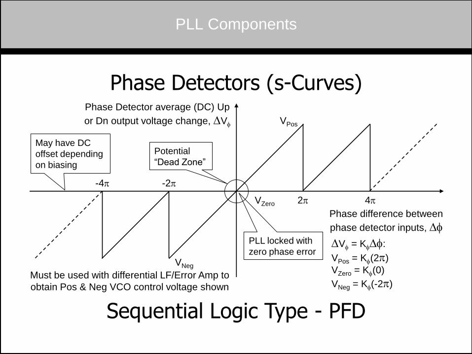
PLL Components
Phase Detectors (s-Curves)
Sequential Logic Type - PFD
Phase Detector average (DC) Up
or Dn output voltage change, DVf
Phase difference between
phase detector inputs, Df
VPos
VZero
VNeg
DVf = KfDf:
VPos = Kf(2p)
VZero = Kf(0)
VNeg = Kf(-2p)
May have DC
offset depending
on biasing
2p 4p
-2p -4p
Potential
“Dead Zone”
PLL locked with
zero phase error
Must be used with differential LF/Error Amp to
obtain Pos & Neg VCO control voltage shown
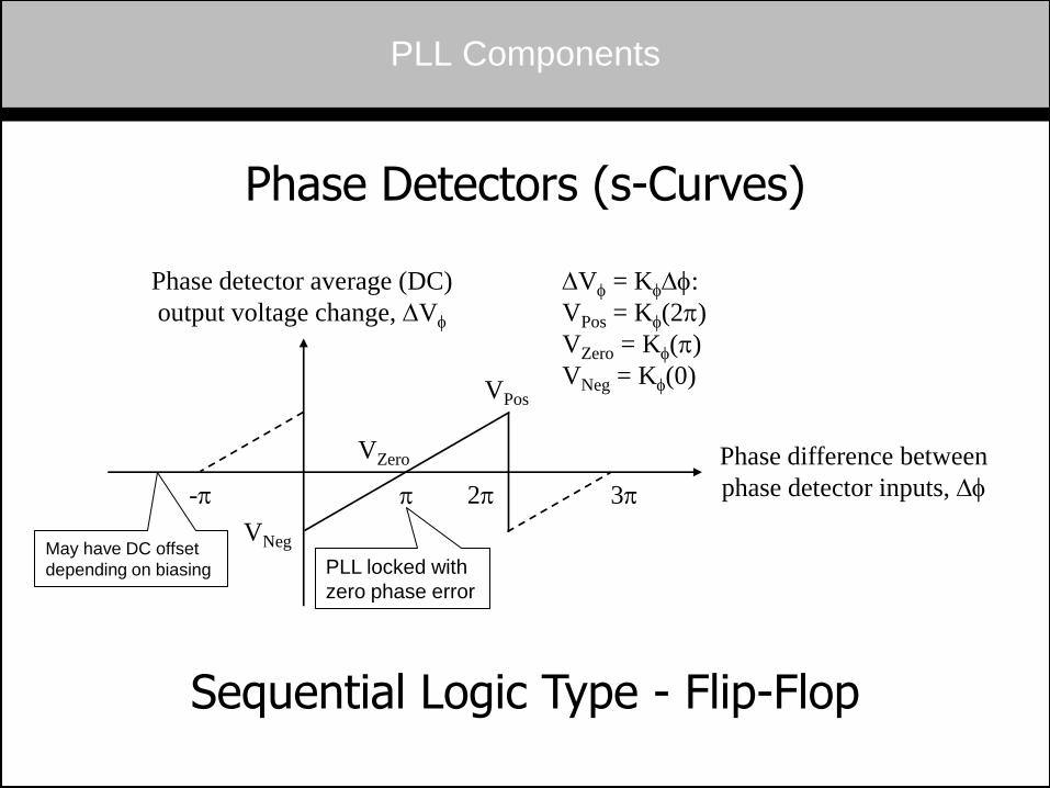
PLL Components
Phase Detectors (s-Curves)
Sequential Logic Type - Flip-Flop
Phase detector average (DC)
output voltage change, DVf
Phase difference between
phase detector inputs, Df
DVf = KfDf:
VPos = Kf(2p)
VZero = Kf(p)
VNeg = Kf(0)
May have DC offset
depending on biasing
2p -p p
VPos
VNeg
VZero
3p
PLL locked with
zero phase error
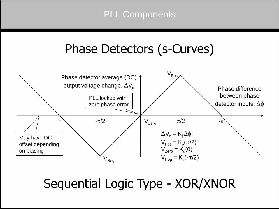
PLL Components
Phase Detectors (s-Curves)
Sequential Logic Type - XOR/XNOR
Phase detector average (DC)
output voltage change, DVf
Phase difference
between phase
detector inputs, Df
DVf = KfDf:
VPos = Kf(p/2)
VZero = Kf(0)
VNeg = Kf(-p/2)
May have DC
offset depending
on biasing
p/2 -p/2 -p p
VPos
VZero
VNeg
PLL locked with
zero phase error
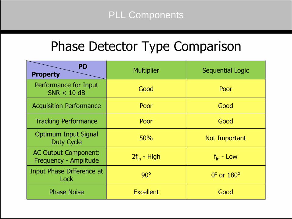
PLL Components
PD Property
Multiplier Sequential Logic
Performance for Input SNR < 10 dB
Good Poor
Acquisition Performance Poor Good
Tracking Performance Poor Good
Optimum Input Signal Duty Cycle
50% Not Important
AC Output Component: Frequency - Amplitude
2fin - High fin - Low
Input Phase Difference at Lock
90o 0o or 180o
Phase Noise Excellent Good
Phase Detector Type Comparison
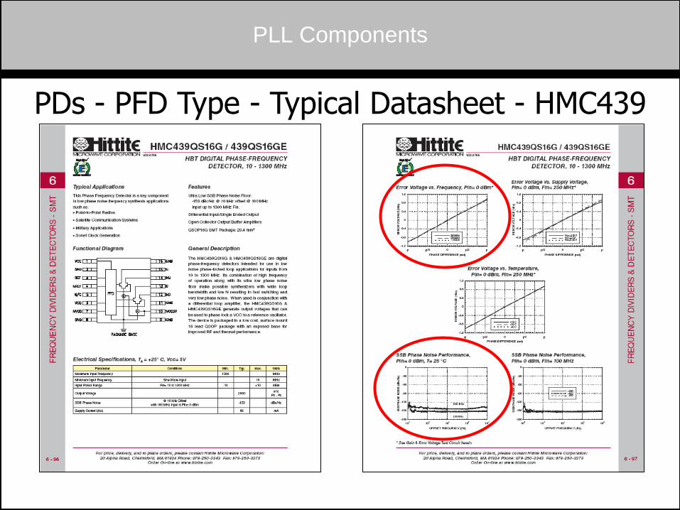
PLL Components
PDs - PFD Type - Typical Datasheet - HMC439
100 MHz
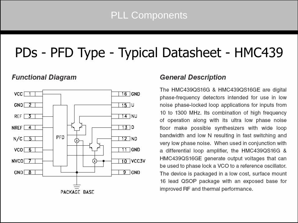
PLL Components
PDs - PFD Type - Typical Datasheet - HMC439
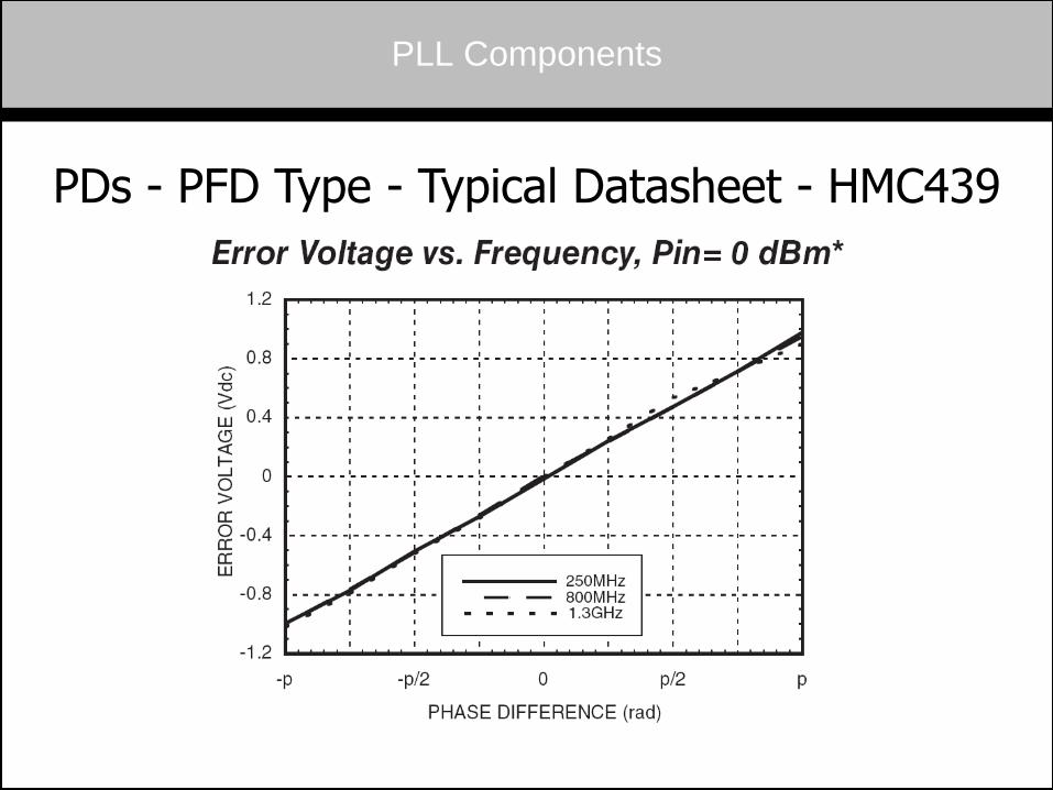
PLL Components
PDs - PFD Type - Typical Datasheet - HMC439
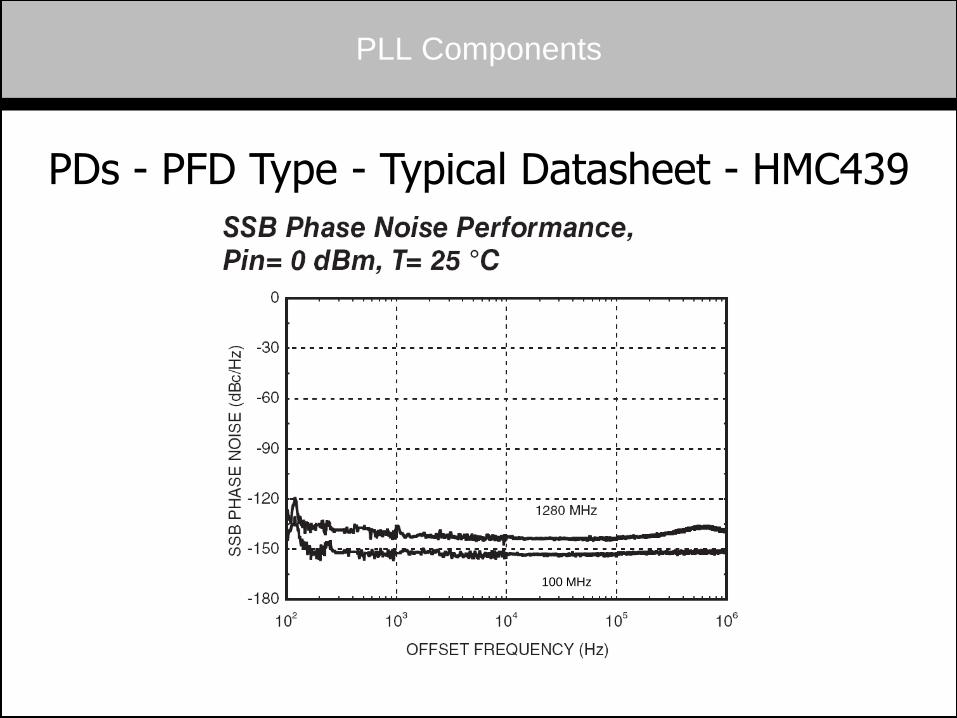
PLL Components
PDs - PFD Type - Typical Datasheet - HMC439
100 MHz
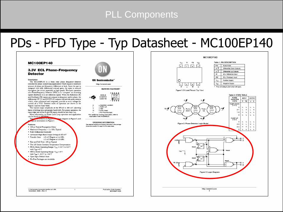
PLL Components
PDs - PFD Type - Typ Datasheet - MC100EP140
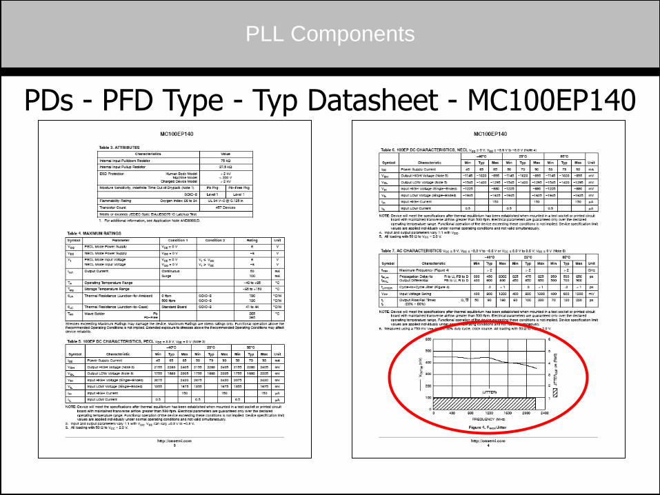
PLL Components
PDs - PFD Type - Typ Datasheet - MC100EP140
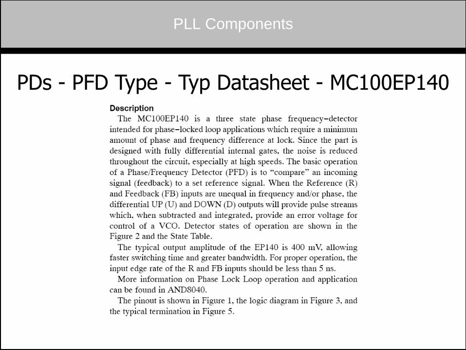
PLL Components
PDs - PFD Type - Typ Datasheet - MC100EP140
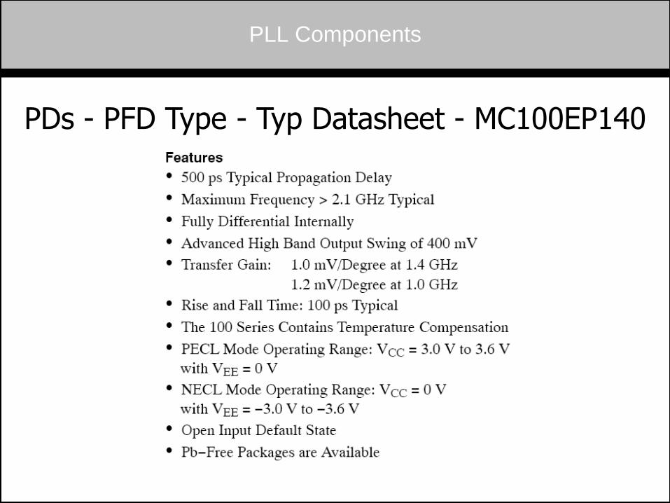
PLL Components
PDs - PFD Type - Typ Datasheet - MC100EP140
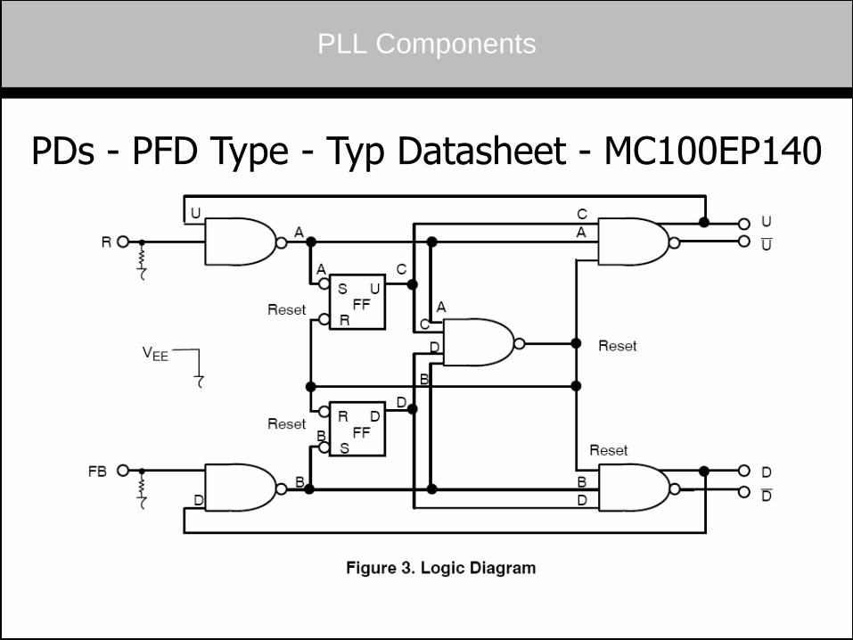
PLL Components
PDs - PFD Type - Typ Datasheet - MC100EP140
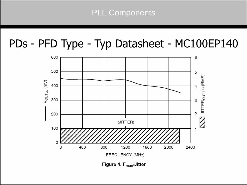
PLL Components
PDs - PFD Type - Typ Datasheet - MC100EP140
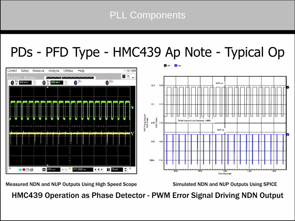
PLL Components
PDs - PFD Type - HMC439 Ap Note - Typical Op
Measured NDN and NUP Outputs Using High Speed Scope Simulated NDN and NUP Outputs Using SPICE
HMC439 Operation as Phase Detector - PWM Error Signal Driving NDN Output
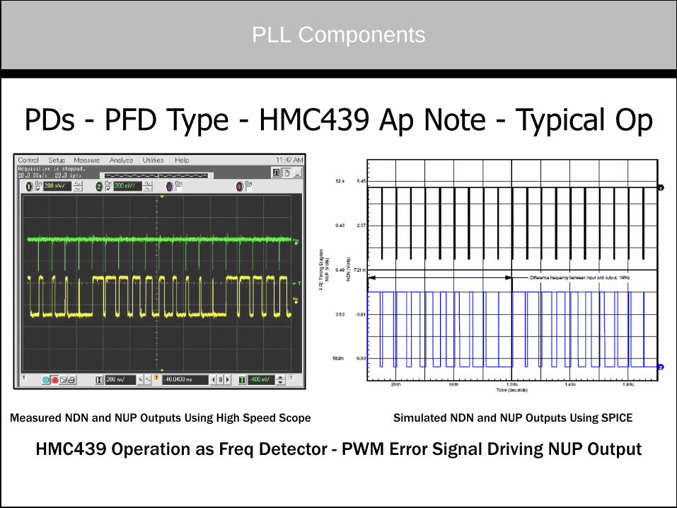
PLL Components
Measured NDN and NUP Outputs Using High Speed Scope Simulated NDN and NUP Outputs Using SPICE
HMC439 Operation as Freq Detector - PWM Error Signal Driving NUP Output
PDs - PFD Type - HMC439 Ap Note - Typical Op
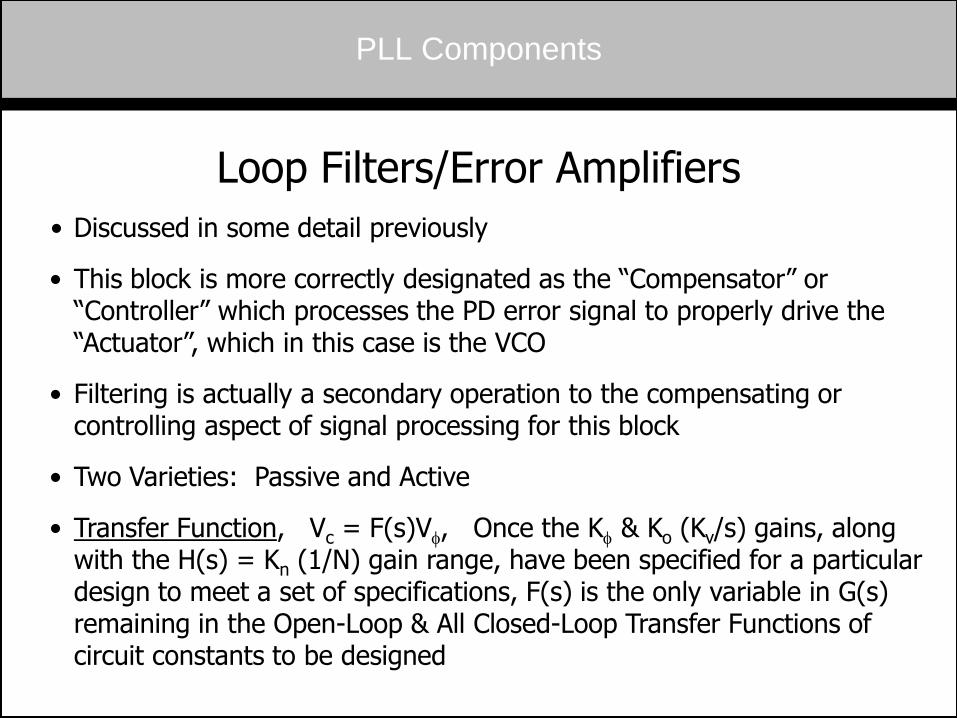
PLL Components
Loop Filters/Error Amplifiers
• Discussed in some detail previously
• This block is more correctly designated as the “Compensator” or “Controller” which processes the PD error signal to properly drive the “Actuator”, which in this case is the VCO
• Filtering is actually a secondary operation to the compensating or controlling aspect of signal processing for this block
• Two Varieties: Passive and Active
• Transfer Function, Vc = F(s)Vf, Once the Kf & Ko (Kv/s) gains, along with the H(s) = Kn (1/N) gain range, have been specified for a particular design to meet a set of specifications, F(s) is the only variable in G(s) remaining in the Open-Loop & All Closed-Loop Transfer Functions of circuit constants to be designed
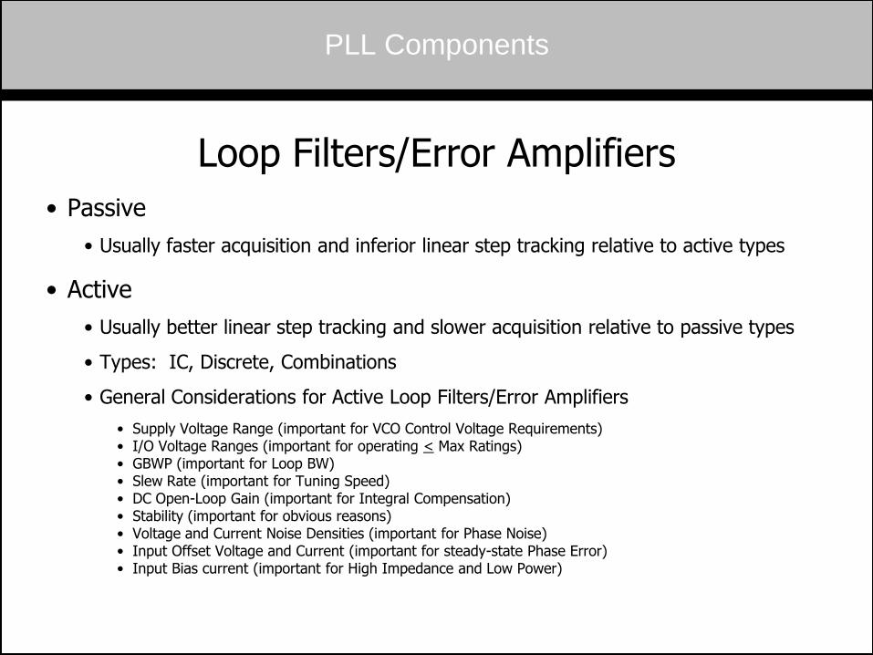
PLL Components
Loop Filters/Error Amplifiers
• Passive
• Usually faster acquisition and inferior linear step tracking relative to active types
• Active
• Usually better linear step tracking and slower acquisition relative to passive types
• Types: IC, Discrete, Combinations
• General Considerations for Active Loop Filters/Error Amplifiers
• Supply Voltage Range (important for VCO Control Voltage Requirements) • I/O Voltage Ranges (important for operating < Max Ratings) • GBWP (important for Loop BW) • Slew Rate (important for Tuning Speed) • DC Open-Loop Gain (important for Integral Compensation) • Stability (important for obvious reasons) • Voltage and Current Noise Densities (important for Phase Noise) • Input Offset Voltage and Current (important for steady-state Phase Error) • Input Bias current (important for High Impedance and Low Power)
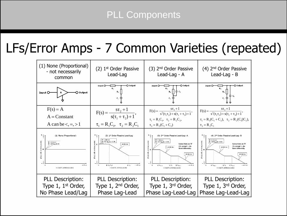
PLL Components
LFs/Error Amps - 7 Common Varieties (repeated) (1) None (Proportional)
- not necessarily common
(2) 1st Order Passive Lead-Lag
(3) 2nd Order Passive Lead-Lag - A
(4) 2nd Order Passive Lead-Lag - B
PLL Description: Type 1, 1st Order,
No Phase Lead/Lag
PLL Description: Type 1, 2nd Order, Phase Lag-Lead
PLL Description: Type 1, 3rd Order,
Phase Lag-Lead-Lag
PLL Description: Type 1, 3rd Order,
Phase Lag-Lead-Lag
122111
21
2
CR, τCRτ
,1)τ s(τ
1sτF(s)
)C(CRτ
,CR, τCRτ
,1)τs(τ)τ(τ s
1sτF(s)
2123
222111
3121
2
3
1 , , becan A
Constant A
AF(s)
123
21222111
3121
2
3
CRτ
),||C(CR), τC(CRτ
,1)τs(τ)τ(τ s
1sτF(s)
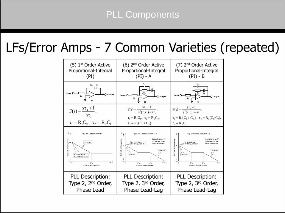
PLL Components
LFs/Error Amps - 7 Common Varieties (repeated) (5) 1st Order Active
Proportional-Integral (PI)
(6) 2nd Order Active Proportional-Integral
(PI) - A
(7) 2nd Order Active Proportional-Integral
(PI) - B
PLL Description: Type 2, 2nd Order,
Phase Lead
PLL Description: Type 2, 3rd Order, Phase Lead-Lag
PLL Description: Type 2, 3rd Order, Phase Lead-Lag
122111
1
2
CR, τCRτ
, sτ
1sτF(s)
)C(CRτ
,CR, τCRτ
,sτ)τ(τ s
1sτF(s)
2123
222111
121
2
3
123
21222111
121
2
3
CRτ
),||C(CR, τCCRτ
,sτ)τ(τ s
1sτF(s)
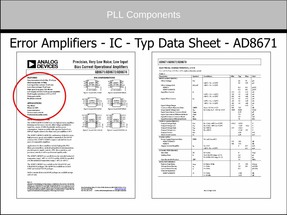
PLL Components
Error Amplifiers - IC - Typ Data Sheet - AD8671
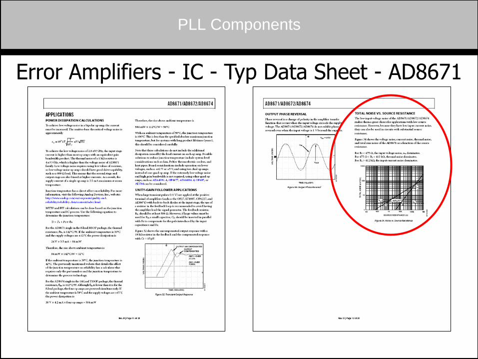
PLL Components
Error Amplifiers - IC - Typ Data Sheet - AD8671
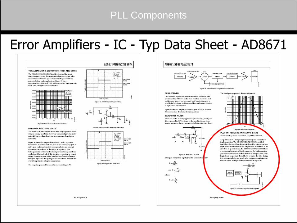
PLL Components
Error Amplifiers - IC - Typ Data Sheet - AD8671
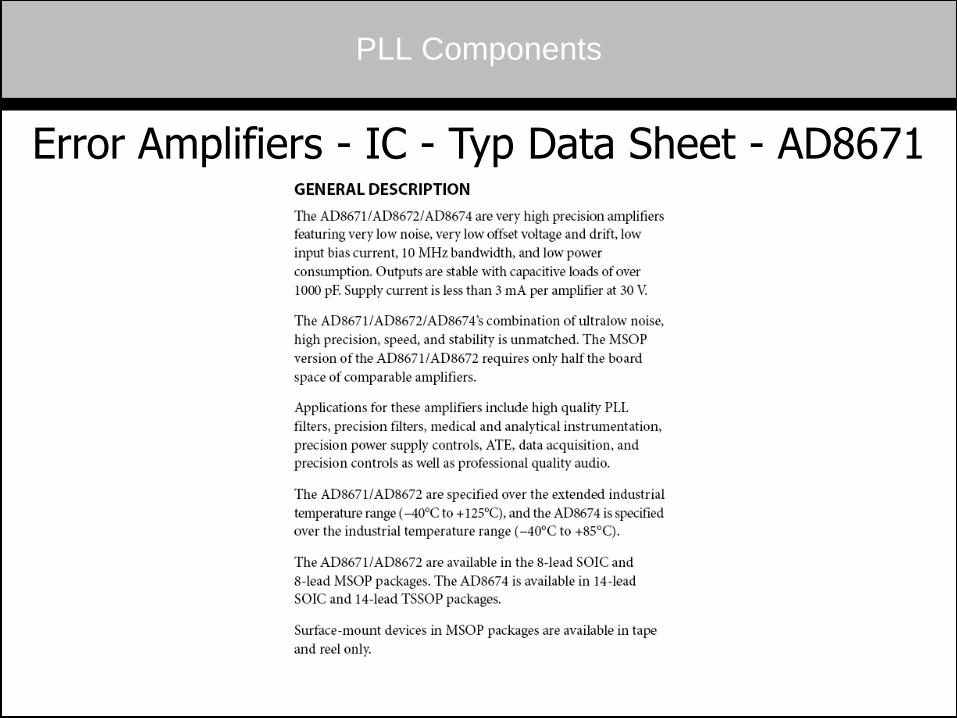
PLL Components
Error Amplifiers - IC - Typ Data Sheet - AD8671
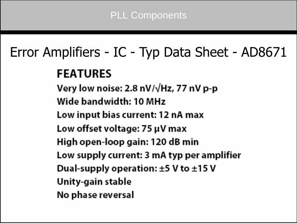
PLL Components
Error Amplifiers - IC - Typ Data Sheet - AD8671
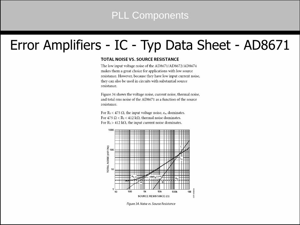
PLL Components
Error Amplifiers - IC - Typ Data Sheet - AD8671
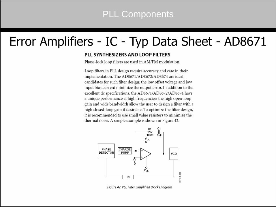
PLL Components
Error Amplifiers - IC - Typ Data Sheet - AD8671
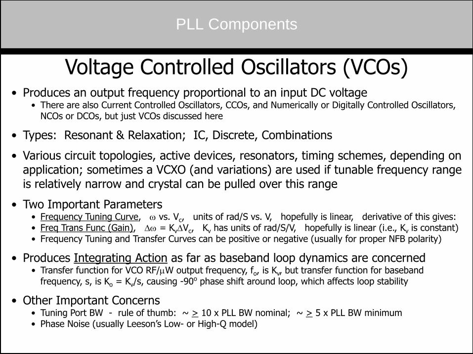
PLL Components
Voltage Controlled Oscillators (VCOs)
• Produces an output frequency proportional to an input DC voltage • There are also Current Controlled Oscillators, CCOs, and Numerically or Digitally Controlled Oscillators,
NCOs or DCOs, but just VCOs discussed here
• Types: Resonant & Relaxation; IC, Discrete, Combinations
• Various circuit topologies, active devices, resonators, timing schemes, depending on application; sometimes a VCXO (and variations) are used if tunable frequency range is relatively narrow and crystal can be pulled over this range
• Two Important Parameters • Frequency Tuning Curve, w vs. Vc, units of rad/S vs. V, hopefully is linear, derivative of this gives: • Freq Trans Func (Gain), Dw = KvDVc, Kv has units of rad/S/V, hopefully is linear (i.e., Kv is constant) • Frequency Tuning and Transfer Curves can be positive or negative (usually for proper NFB polarity)
• Produces Integrating Action as far as baseband loop dynamics are concerned • Transfer function for VCO RF/mW output frequency, fo, is Kv, but transfer function for baseband
frequency, s, is Ko = Kv/s, causing -90o phase shift around loop, which affects loop stability
• Other Important Concerns • Tuning Port BW - rule of thumb: ~ > 10 x PLL BW nominal; ~ > 5 x PLL BW minimum • Phase Noise (usually Leeson’s Low- or High-Q model)
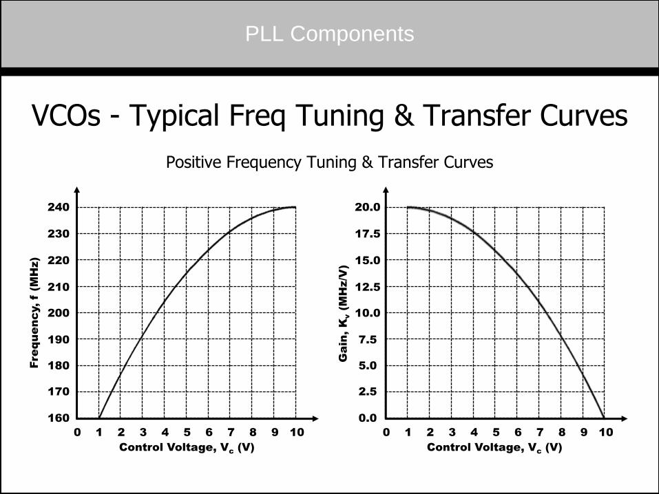
PLL Components
VCOs - Typical Freq Tuning & Transfer Curves
Fre
qu
en
cy, f (M
Hz)
Ga
in
, K
v (M
Hz/V
)
Control Voltage, Vc (V)
0 1 2 3 4 5 6 7 8 9 10
160
240
230
220
210
200
190
180
170
Control Voltage, Vc (V)
0 1 2 3 4 5 6 7 8 9 10
0.0
20.0
17.5
15.0
12.5
10.0
7.5
5.0
2.5
Positive Frequency Tuning & Transfer Curves
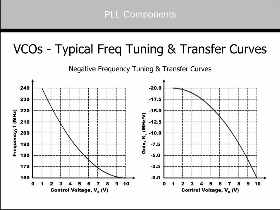
PLL Components
VCOs - Typical Freq Tuning & Transfer Curves
Fre
qu
en
cy, f (M
Hz)
Ga
in
, K
v (M
Hz/V
)
Control Voltage, Vc (V)
0 1 2 3 4 5 6 7 8 9 10
160
240
230
220
210
200
190
180
170
Control Voltage, Vc (V)
0 1 2 3 4 5 6 7 8 9 10
-0.0
-20.0
-17.5
-15.0
-12.5
-10.0
-7.5
-5.0
-2.5
Negative Frequency Tuning & Transfer Curves
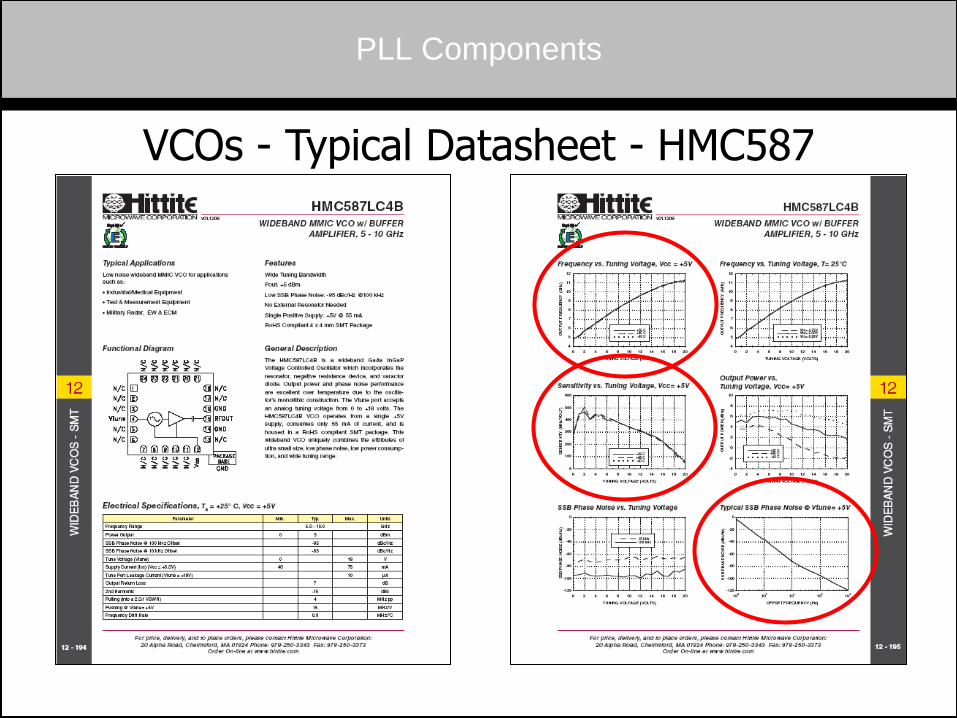
PLL Components
VCOs - Typical Datasheet - HMC587
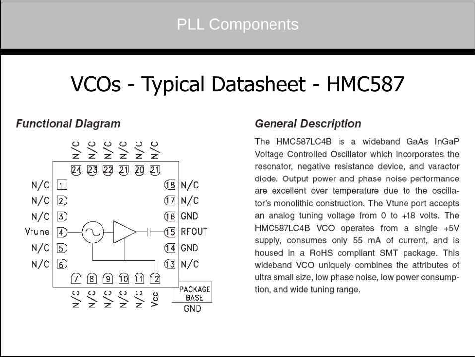
PLL Components
VCOs - Typical Datasheet - HMC587
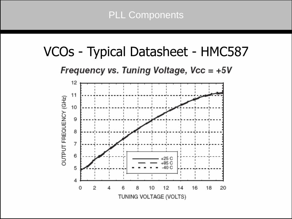
PLL Components
VCOs - Typical Datasheet - HMC587
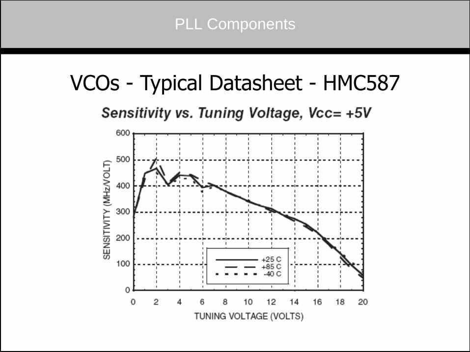
PLL Components
VCOs - Typical Datasheet - HMC587
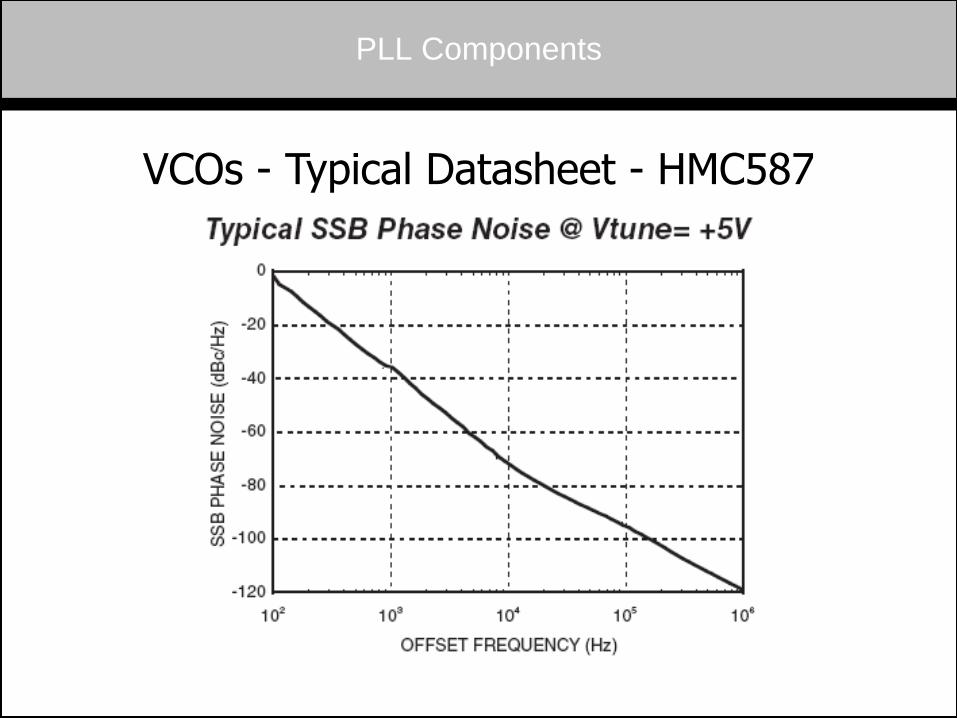
PLL Components
VCOs - Typical Datasheet - HMC587
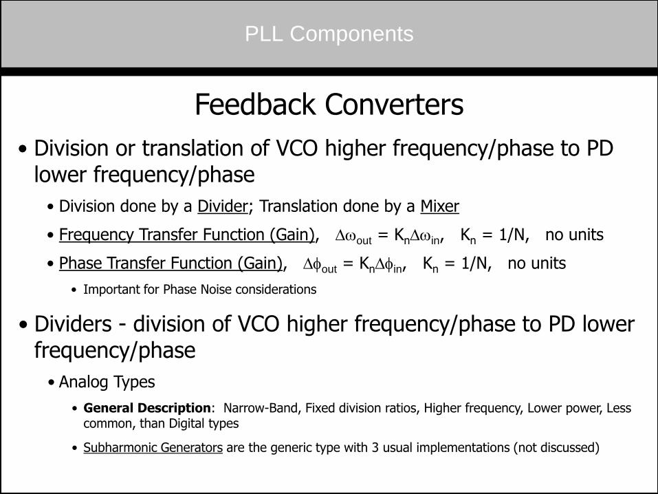
PLL Components
Feedback Converters
• Division or translation of VCO higher frequency/phase to PD lower frequency/phase
• Division done by a Divider; Translation done by a Mixer
• Frequency Transfer Function (Gain), Dwout = KnDwin, Kn = 1/N, no units
• Phase Transfer Function (Gain), Dfout = KnDfin, Kn = 1/N, no units
• Important for Phase Noise considerations
• Dividers - division of VCO higher frequency/phase to PD lower frequency/phase
• Analog Types
• General Description: Narrow-Band, Fixed division ratios, Higher frequency, Lower power, Less common, than Digital types
• Subharmonic Generators are the generic type with 3 usual implementations (not discussed)
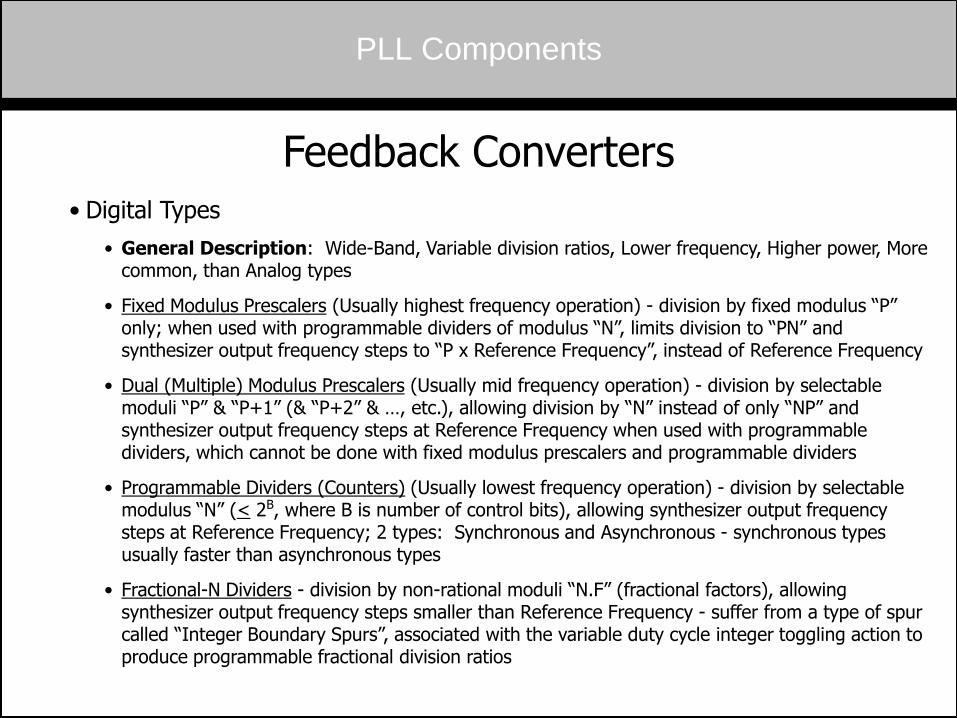
PLL Components
Feedback Converters
• Digital Types
• General Description: Wide-Band, Variable division ratios, Lower frequency, Higher power, More common, than Analog types
• Fixed Modulus Prescalers (Usually highest frequency operation) - division by fixed modulus “P” only; when used with programmable dividers of modulus “N”, limits division to “PN” and synthesizer output frequency steps to “P x Reference Frequency”, instead of Reference Frequency
• Dual (Multiple) Modulus Prescalers (Usually mid frequency operation) - division by selectable moduli “P” & “P+1” (& “P+2” & …, etc.), allowing division by “N” instead of only “NP” and synthesizer output frequency steps at Reference Frequency when used with programmable dividers, which cannot be done with fixed modulus prescalers and programmable dividers
• Programmable Dividers (Counters) (Usually lowest frequency operation) - division by selectable modulus “N” (< 2B, where B is number of control bits), allowing synthesizer output frequency steps at Reference Frequency; 2 types: Synchronous and Asynchronous - synchronous types usually faster than asynchronous types
• Fractional-N Dividers - division by non-rational moduli “N.F” (fractional factors), allowing synthesizer output frequency steps smaller than Reference Frequency - suffer from a type of spur called “Integer Boundary Spurs”, associated with the variable duty cycle integer toggling action to produce programmable fractional division ratios
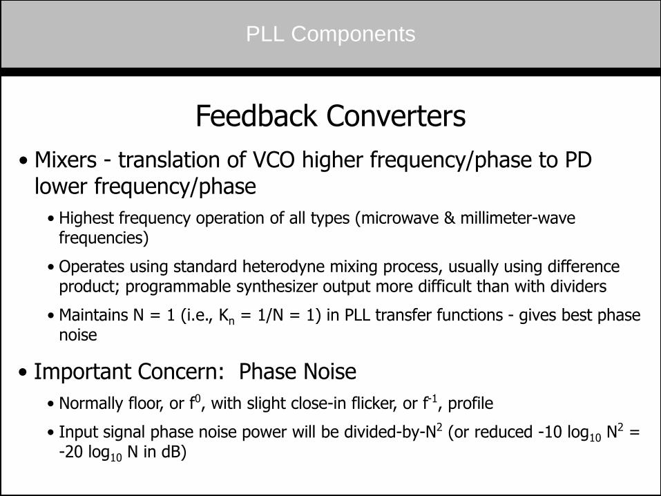
PLL Components
Feedback Converters
• Mixers - translation of VCO higher frequency/phase to PD lower frequency/phase
• Highest frequency operation of all types (microwave & millimeter-wave frequencies)
• Operates using standard heterodyne mixing process, usually using difference product; programmable synthesizer output more difficult than with dividers
• Maintains N = 1 (i.e., Kn = 1/N = 1) in PLL transfer functions - gives best phase noise
• Important Concern: Phase Noise
• Normally floor, or f0, with slight close-in flicker, or f-1, profile
• Input signal phase noise power will be divided-by-N2 (or reduced -10 log10 N2 =
-20 log10 N in dB)
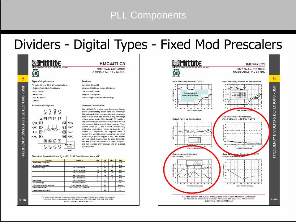
PLL Components
Dividers - Digital Types - Fixed Mod Prescalers
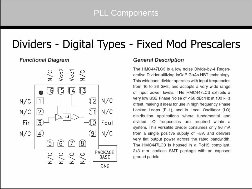
PLL Components
Dividers - Digital Types - Fixed Mod Prescalers
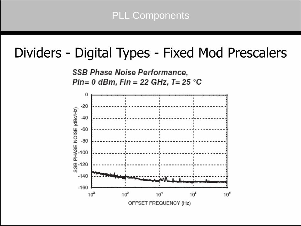
PLL Components
Dividers - Digital Types - Fixed Mod Prescalers
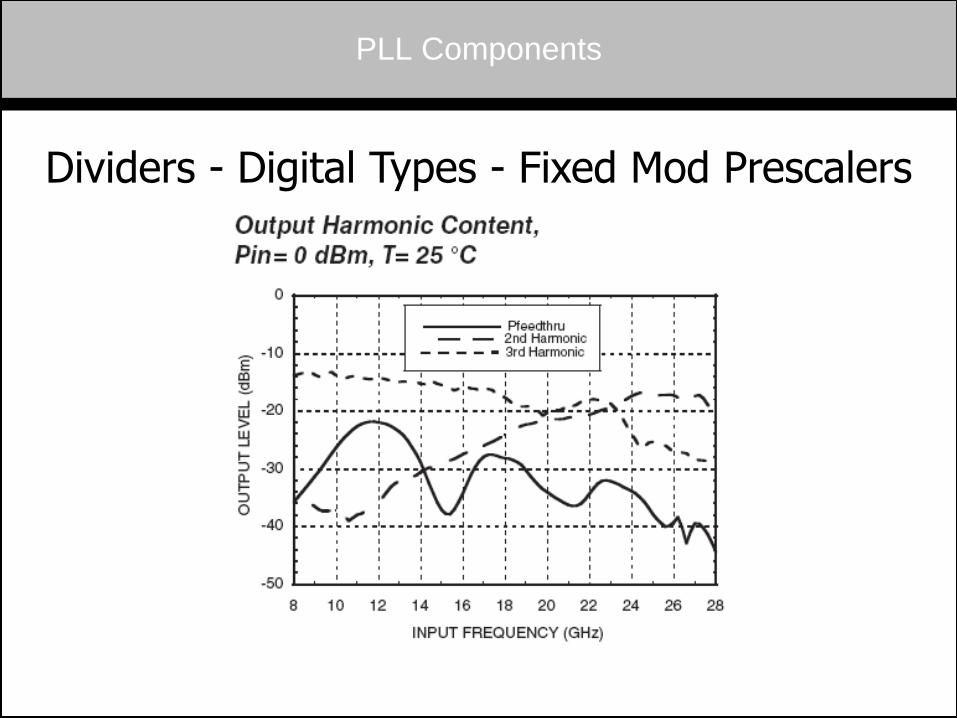
PLL Components
Dividers - Digital Types - Fixed Mod Prescalers
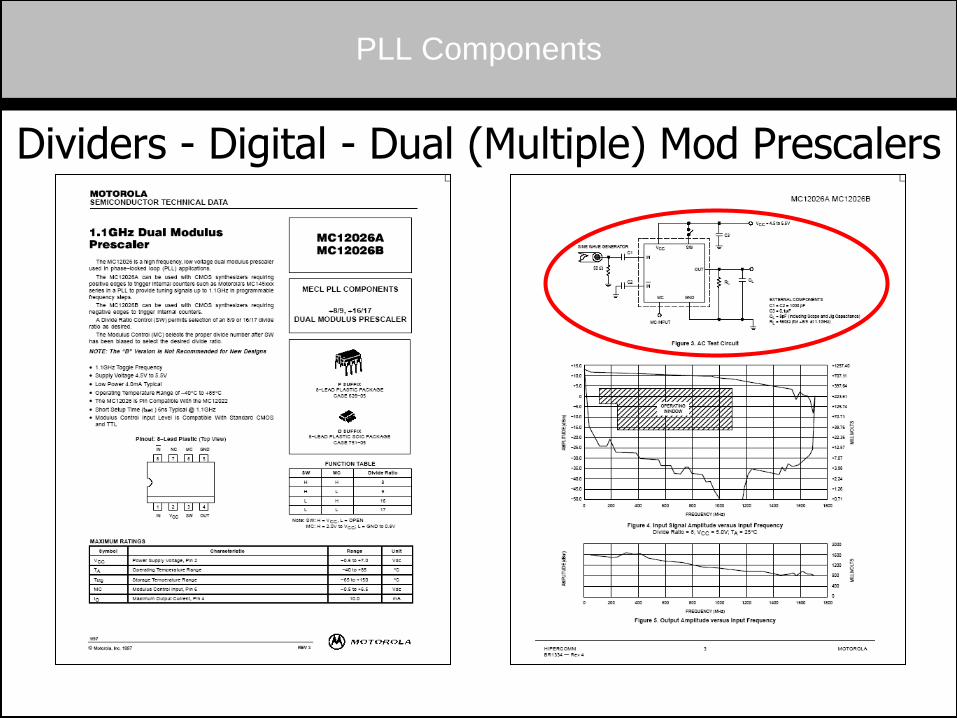
PLL Components
Dividers - Digital - Dual (Multiple) Mod Prescalers
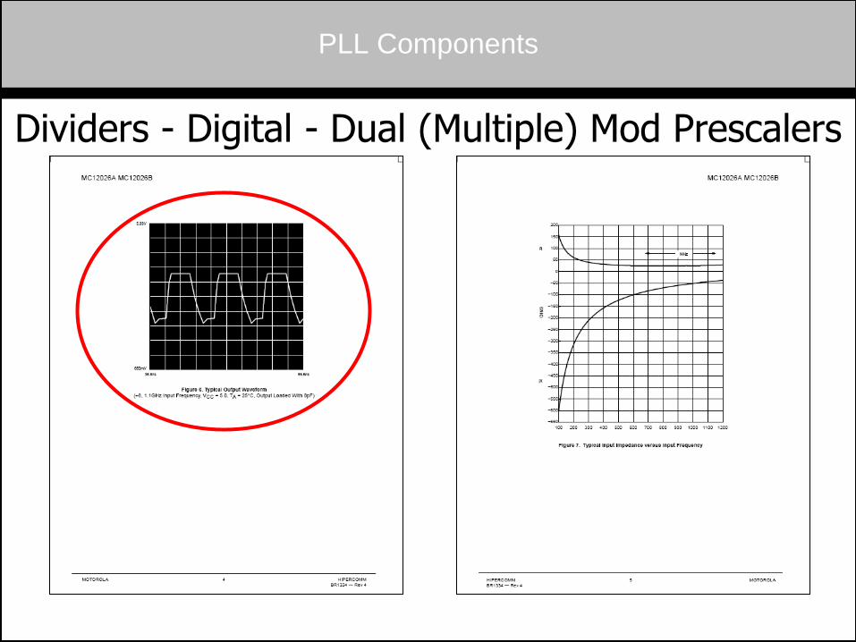
PLL Components
Dividers - Digital - Dual (Multiple) Mod Prescalers
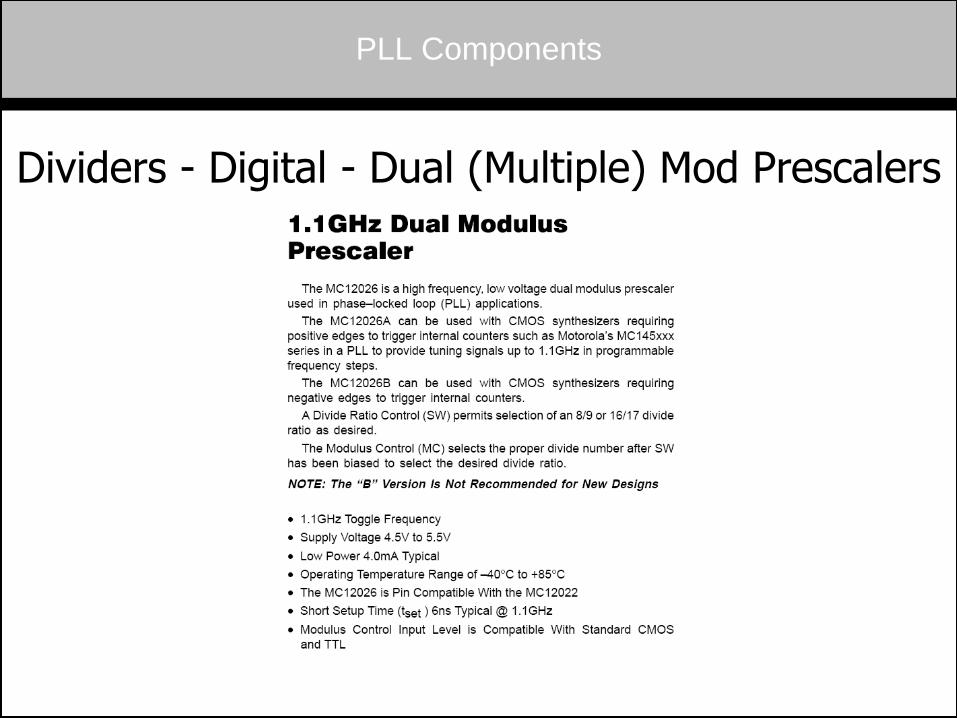
PLL Components
Dividers - Digital - Dual (Multiple) Mod Prescalers
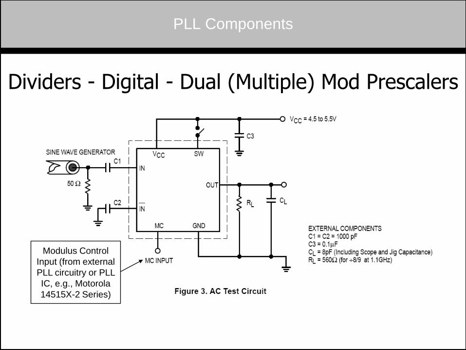
PLL Components
Dividers - Digital - Dual (Multiple) Mod Prescalers
Modulus Control
Input (from external
PLL circuitry or PLL
IC, e.g., Motorola
14515X-2 Series)
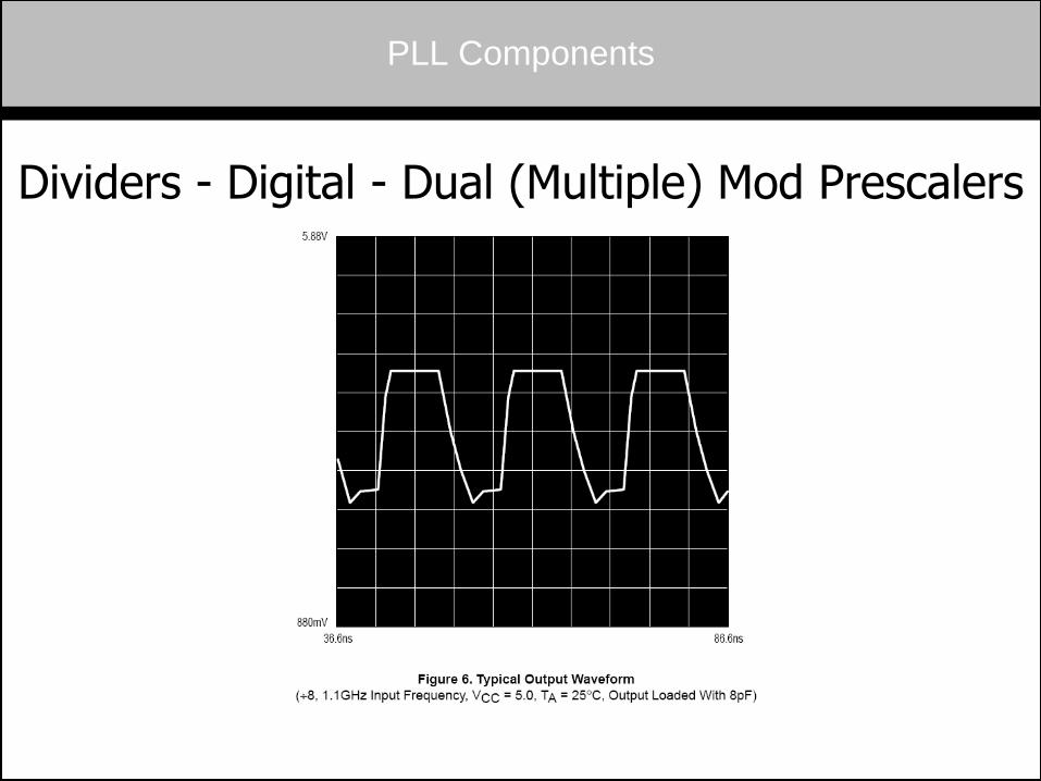
PLL Components
Dividers - Digital - Dual (Multiple) Mod Prescalers
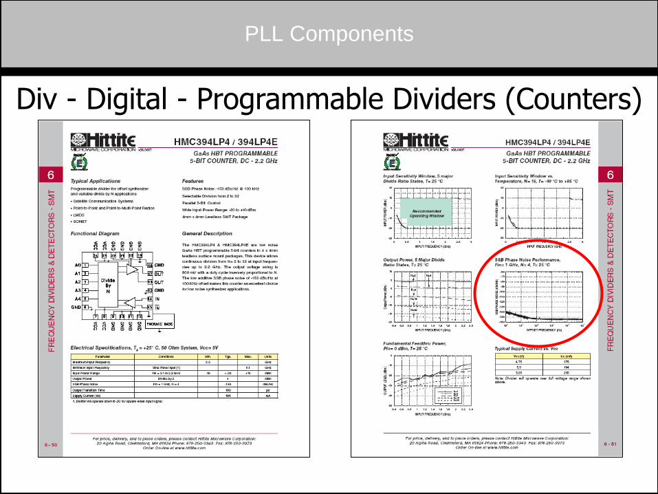
PLL Components
Div - Digital - Programmable Dividers (Counters)
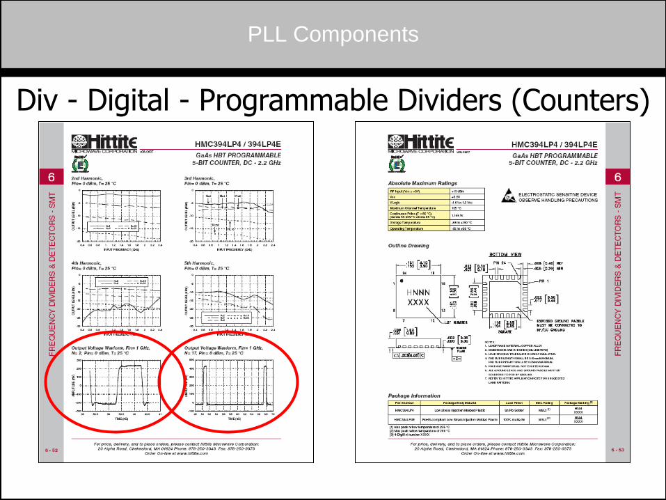
PLL Components
Div - Digital - Programmable Dividers (Counters)
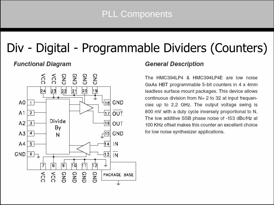
PLL Components
Div - Digital - Programmable Dividers (Counters)
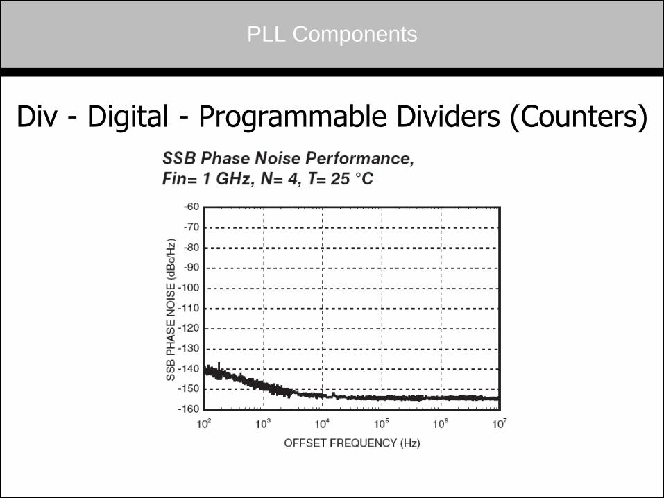
PLL Components
Div - Digital - Programmable Dividers (Counters)
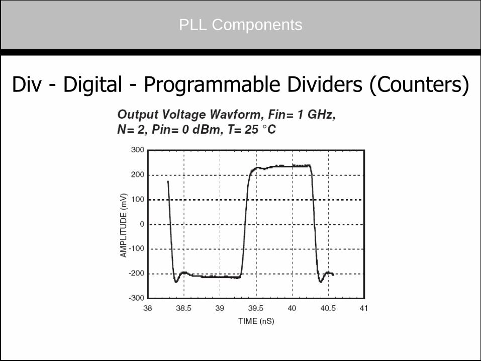
PLL Components
Div - Digital - Programmable Dividers (Counters)
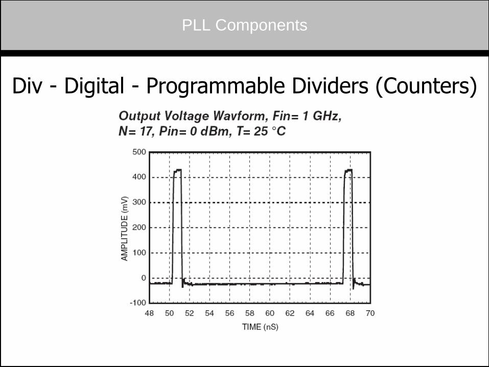
PLL Components
Div - Digital - Programmable Dividers (Counters)
PLL Synthesizer Testing
External (Synth) Performance Measurements
• SSB Phase Noise
• Direct - Spectrum Analyzer for Carrier (RF) Measurement (Note: spec an does not phase-lock to carrier as in some indirect methods)
• Spec Ans With Optional SSB Phase Noise Utility - straight-forward, log frequency scale, 1 Hz BW, must make sure spec an internal phase noise significantly less (< 10 dB) than UUT phase noise
• Spec Ans Without Optional SSB Phase Noise Utility - not straight-forward, may not have log frequency scale, complicated by fact that RBW on most spec ans does not go down to 1 Hz, which is needed for proper measurement, so measurement at RBWs other than 1 Hz must be normalized to measurement referenced to RBW of 1 Hz, must make sure spec an internal phase noise significantly less (< 10 dB) than UUT phase noise
• Indirect - Discrete Set-up or Instrumentation for Baseband (PM) Measurement
• In both cases DSB Phase Noise is actually measured; 3 dB is subtracted for SSB Phase Noise
• Discrete Set-up (3 dB must be subtracted manually)
• Open-Loop Quadrature PM Demodulator (not phase-locked measurement)
• Closed-Loop Quadrature PM Demodulator (is phase-locked measurement)
• Dedicated Instrumentation (3 dB subtracted mathematically by instrument)
• Example: Agilent E5052B Signal Source Analyzer (is phase-locked measurement)
PLL Synthesizer Testing
SSB Phase Noise - Direct - Spec An Measurement
PLL Synthesizer Testing
SSB Phase Noise - Direct - Spec An Measurement
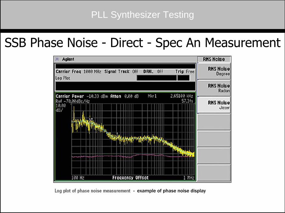
PLL Synthesizer Testing
SSB Phase Noise - Direct - Spec An Measurement
- example of phase noise display
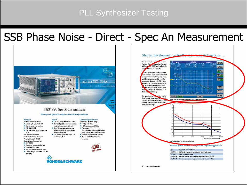
PLL Synthesizer Testing
SSB Phase Noise - Direct - Spec An Measurement
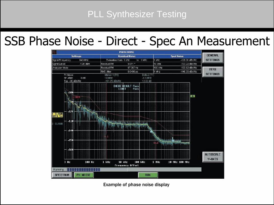
PLL Synthesizer Testing
SSB Phase Noise - Direct - Spec An Measurement
Example of phase noise display
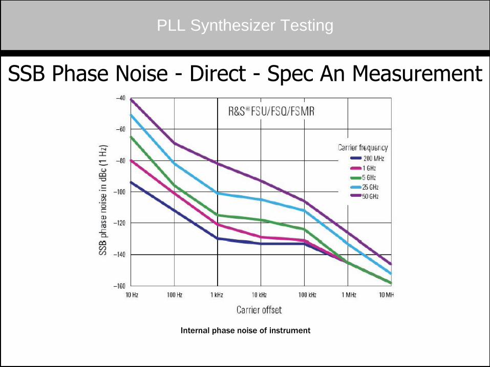
PLL Synthesizer Testing
SSB Phase Noise - Direct - Spec An Measurement
Internal phase noise of instrument
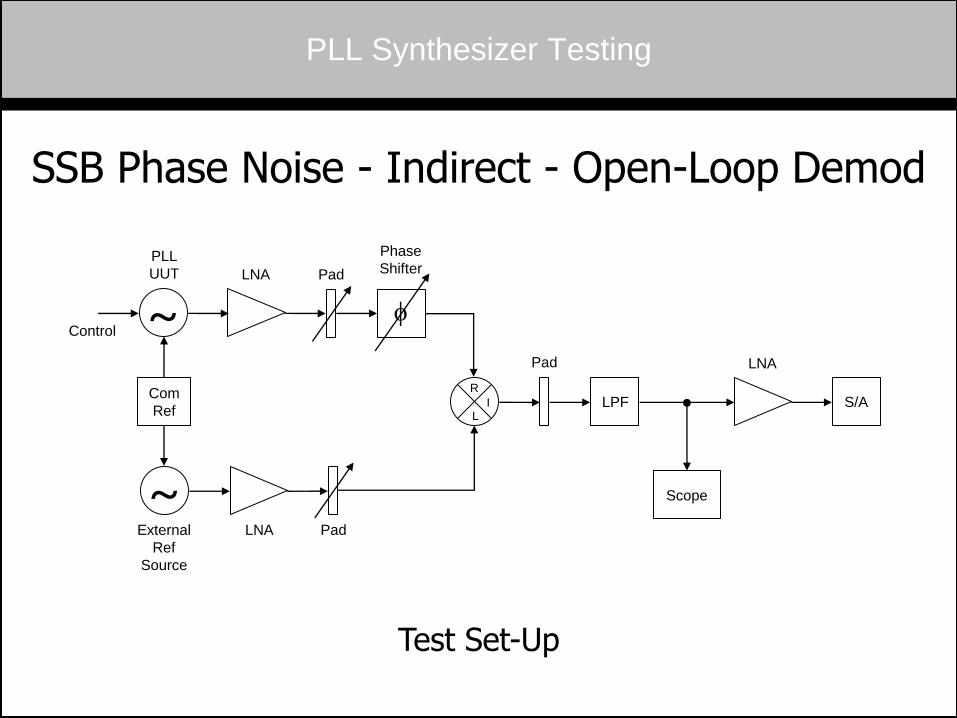
PLL Synthesizer Testing
SSB Phase Noise - Indirect - Open-Loop Demod
S/A Com
Ref LPF
~
f ~
Scope
PLL
UUT
External
Ref
Source
Control
LNA
LNA
Test Set-Up
L
R
I
Pad
Pad
Phase
Shifter
Pad LNA
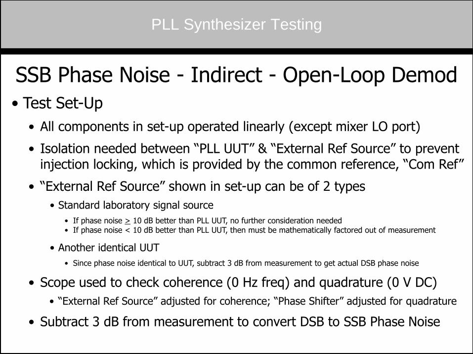
PLL Synthesizer Testing
SSB Phase Noise - Indirect - Open-Loop Demod
• Test Set-Up
• All components in set-up operated linearly (except mixer LO port)
• Isolation needed between “PLL UUT” & “External Ref Source” to prevent injection locking, which is provided by the common reference, “Com Ref”
• “External Ref Source” shown in set-up can be of 2 types
• Standard laboratory signal source
• If phase noise > 10 dB better than PLL UUT, no further consideration needed • If phase noise < 10 dB better than PLL UUT, then must be mathematically factored out of measurement
• Another identical UUT
• Since phase noise identical to UUT, subtract 3 dB from measurement to get actual DSB phase noise
• Scope used to check coherence (0 Hz freq) and quadrature (0 V DC)
• “External Ref Source” adjusted for coherence; “Phase Shifter” adjusted for quadrature
• Subtract 3 dB from measurement to convert DSB to SSB Phase Noise
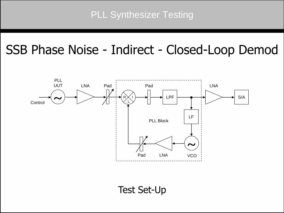
PLL Synthesizer Testing
SSB Phase Noise - Indirect - Closed-Loop Demod
S/A LPF
~
~ LF
PLL
UUT
VCO
Control
Test Set-Up
L
R I
LNA
LNA Pad
Pad Pad LNA
PLL Block
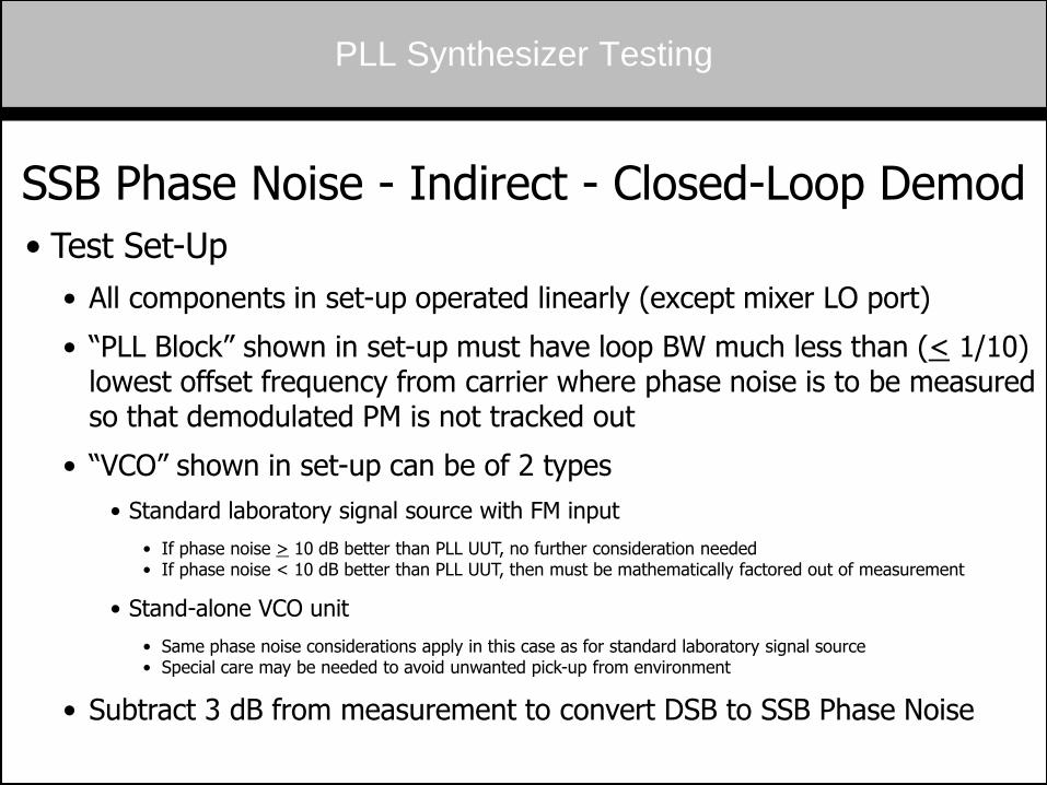
PLL Synthesizer Testing
SSB Phase Noise - Indirect - Closed-Loop Demod
• Test Set-Up
• All components in set-up operated linearly (except mixer LO port)
• “PLL Block” shown in set-up must have loop BW much less than (< 1/10) lowest offset frequency from carrier where phase noise is to be measured so that demodulated PM is not tracked out
• “VCO” shown in set-up can be of 2 types
• Standard laboratory signal source with FM input
• If phase noise > 10 dB better than PLL UUT, no further consideration needed • If phase noise < 10 dB better than PLL UUT, then must be mathematically factored out of measurement
• Stand-alone VCO unit
• Same phase noise considerations apply in this case as for standard laboratory signal source • Special care may be needed to avoid unwanted pick-up from environment
• Subtract 3 dB from measurement to convert DSB to SSB Phase Noise
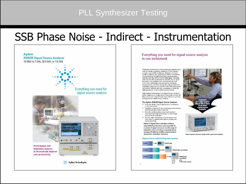
PLL Synthesizer Testing
SSB Phase Noise - Indirect - Instrumentation
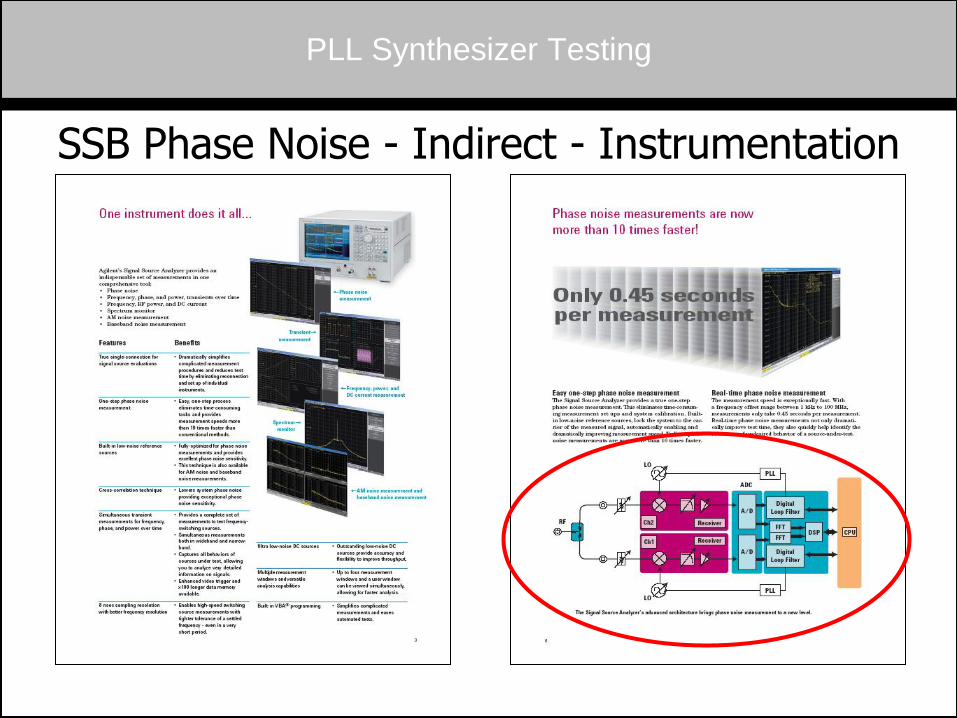
PLL Synthesizer Testing
SSB Phase Noise - Indirect - Instrumentation
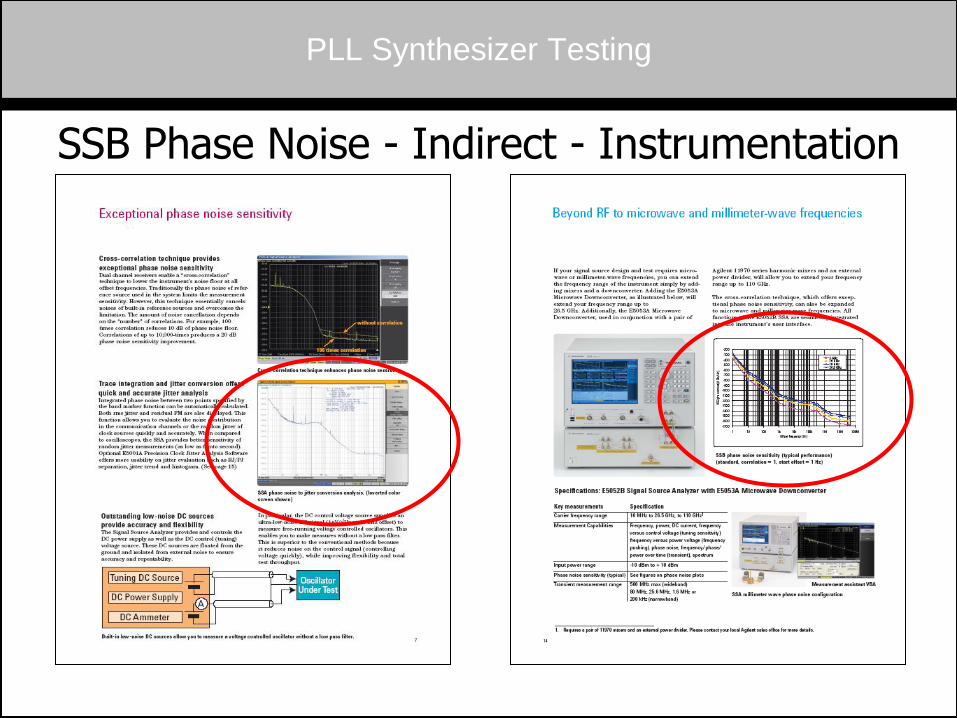
PLL Synthesizer Testing
SSB Phase Noise - Indirect - Instrumentation
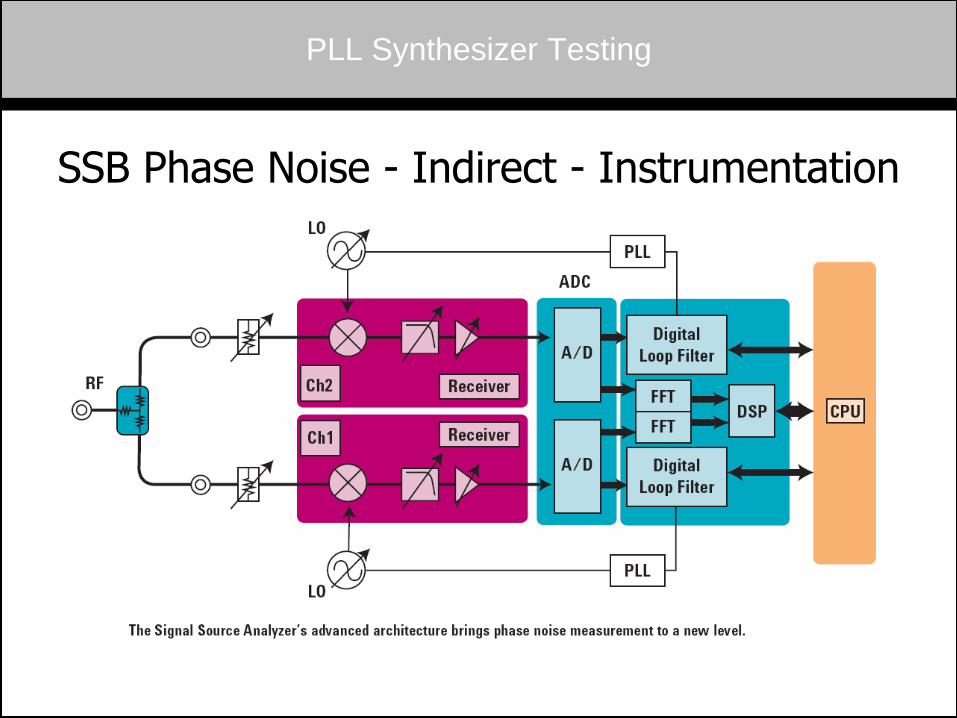
PLL Synthesizer Testing
SSB Phase Noise - Indirect - Instrumentation
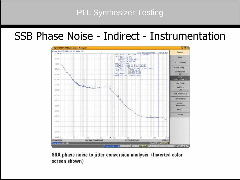
PLL Synthesizer Testing
SSB Phase Noise - Indirect - Instrumentation
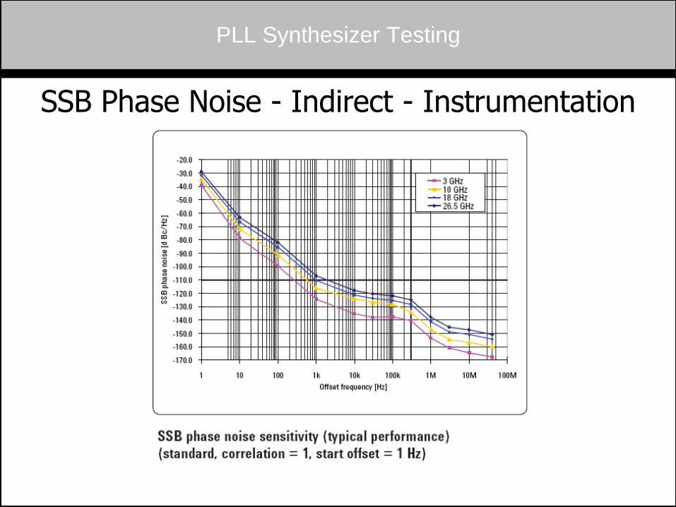
PLL Synthesizer Testing
SSB Phase Noise - Indirect - Instrumentation
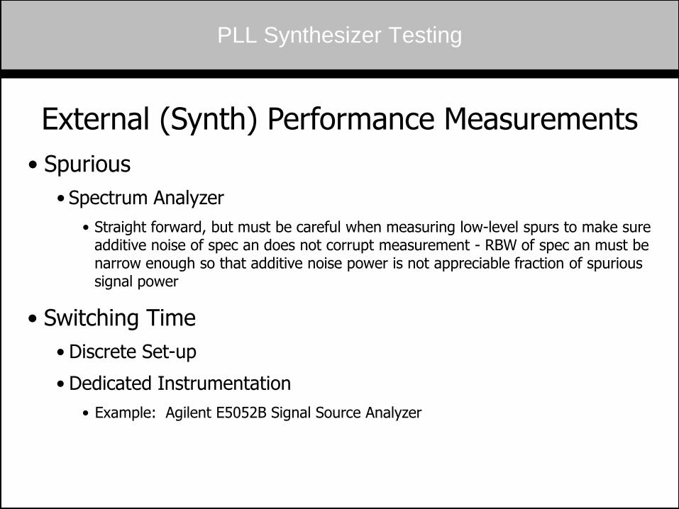
PLL Synthesizer Testing
External (Synth) Performance Measurements
• Spurious
• Spectrum Analyzer
• Straight forward, but must be careful when measuring low-level spurs to make sure additive noise of spec an does not corrupt measurement - RBW of spec an must be narrow enough so that additive noise power is not appreciable fraction of spurious signal power
• Switching Time
• Discrete Set-up
• Dedicated Instrumentation
• Example: Agilent E5052B Signal Source Analyzer
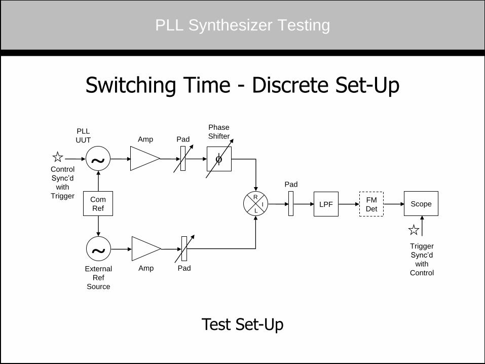
PLL Synthesizer Testing
Switching Time - Discrete Set-Up
Com
Ref LPF
~
~
Scope
PLL
UUT
Trigger
Sync’d
with
Control
Control
Sync’d
with
Trigger
Test Set-Up
L
R
I
External
Ref
Source
Amp
Amp
Pad
Pad
Pad
f
Phase
Shifter
FM
Det
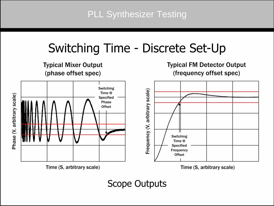
PLL Synthesizer Testing
Switching Time - Discrete Set-Up
Scope Outputs
Typical Mixer Output
(phase offset spec)
Typical FM Detector Output
(frequency offset spec)
Time (S, arbitrary scale) Time (S, arbitrary scale)
Ph
ase
(V, a
rbit
rary
sca
le)
Fre
qu
en
cy
(V, a
rbit
rary
sca
le) Switching
Time @
Specified
Phase
Offset
Switching
Time @
Specified
Frequency
Offset
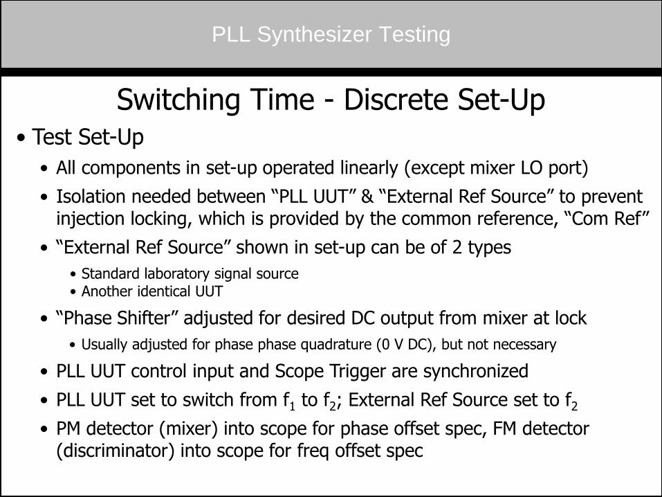
PLL Synthesizer Testing
Switching Time - Discrete Set-Up
• Test Set-Up
• All components in set-up operated linearly (except mixer LO port)
• Isolation needed between “PLL UUT” & “External Ref Source” to prevent injection locking, which is provided by the common reference, “Com Ref”
• “External Ref Source” shown in set-up can be of 2 types
• Standard laboratory signal source • Another identical UUT
• “Phase Shifter” adjusted for desired DC output from mixer at lock
• Usually adjusted for phase phase quadrature (0 V DC), but not necessary
• PLL UUT control input and Scope Trigger are synchronized
• PLL UUT set to switch from f1 to f2; External Ref Source set to f2
• PM detector (mixer) into scope for phase offset spec, FM detector (discriminator) into scope for freq offset spec
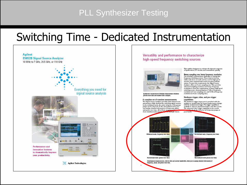
PLL Synthesizer Testing
Switching Time - Dedicated Instrumentation
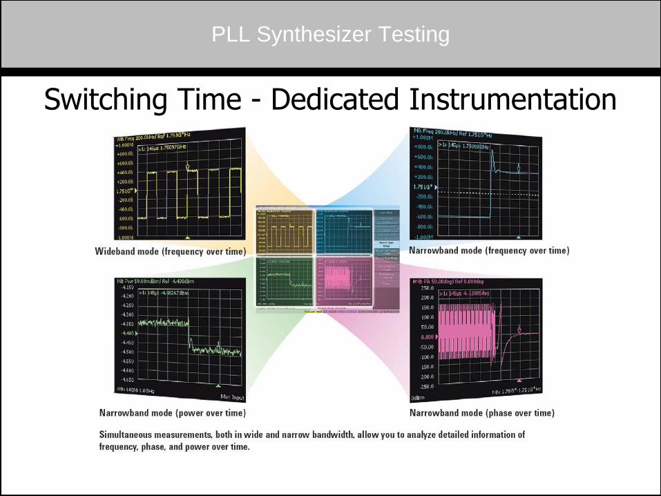
PLL Synthesizer Testing
Switching Time - Dedicated Instrumentation
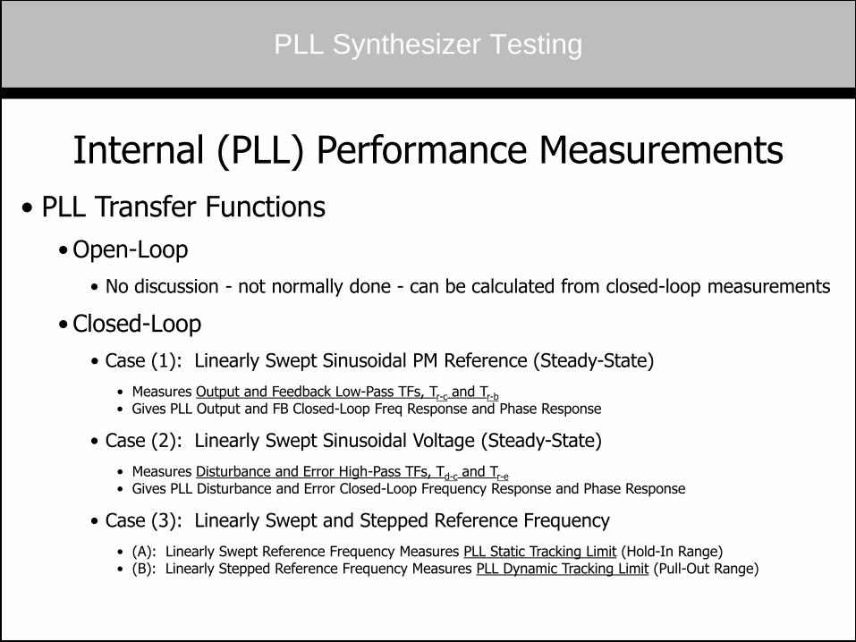
PLL Synthesizer Testing
Internal (PLL) Performance Measurements
• PLL Transfer Functions
• Open-Loop
• No discussion - not normally done - can be calculated from closed-loop measurements
• Closed-Loop
• Case (1): Linearly Swept Sinusoidal PM Reference (Steady-State)
• Measures Output and Feedback Low-Pass TFs, Tr-c and Tr-b • Gives PLL Output and FB Closed-Loop Freq Response and Phase Response
• Case (2): Linearly Swept Sinusoidal Voltage (Steady-State)
• Measures Disturbance and Error High-Pass TFs, Td-c and Tr-e • Gives PLL Disturbance and Error Closed-Loop Frequency Response and Phase Response
• Case (3): Linearly Swept and Stepped Reference Frequency
• (A): Linearly Swept Reference Frequency Measures PLL Static Tracking Limit (Hold-In Range) • (B): Linearly Stepped Reference Frequency Measures PLL Dynamic Tracking Limit (Pull-Out Range)
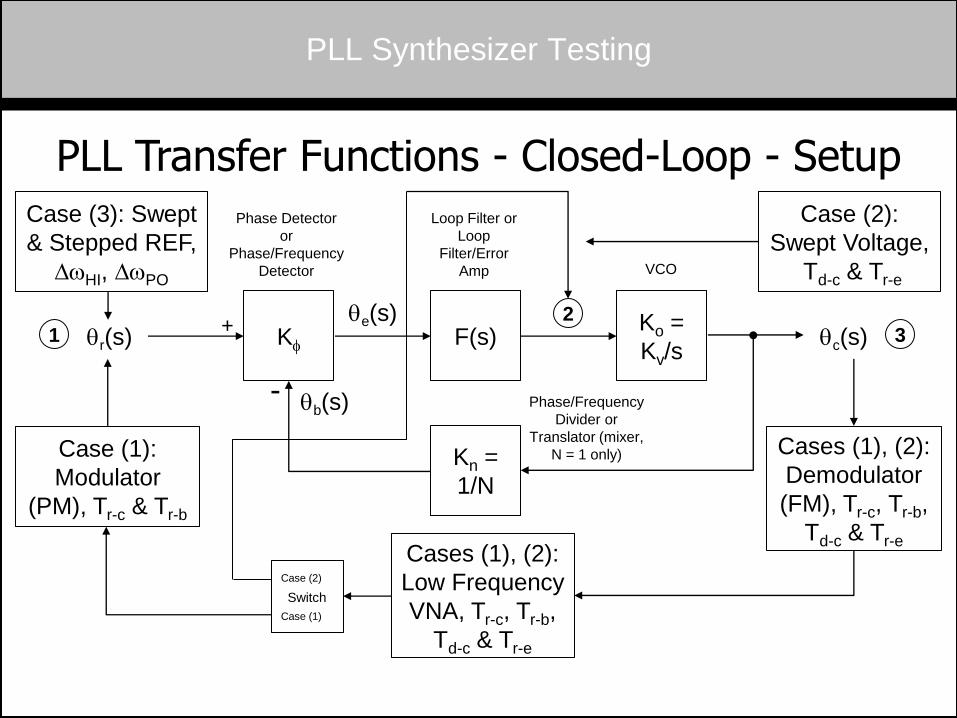
PLL Synthesizer Testing
PLL Transfer Functions - Closed-Loop - Setup
Phase Detector
or
Phase/Frequency
Detector
Loop Filter or
Loop
Filter/Error
Amp
Phase/Frequency
Divider or
Translator (mixer,
N = 1 only)
Ko =
Kv/s
F(s) Kf
Kn =
1/N
VCO
3 2
1 qr(s) qc(s)
qb(s)
qe(s) +
-
Case (1):
Modulator
(PM), Tr-c & Tr-b
Cases (1), (2):
Demodulator
(FM), Tr-c, Tr-b,
Td-c & Tr-e Cases (1), (2):
Low Frequency
VNA, Tr-c, Tr-b,
Td-c & Tr-e
Case (3): Swept
& Stepped REF,
DwHI, DwPO
Case (2):
Swept Voltage,
Td-c & Tr-e
Case (2)
Case (1)
Switch
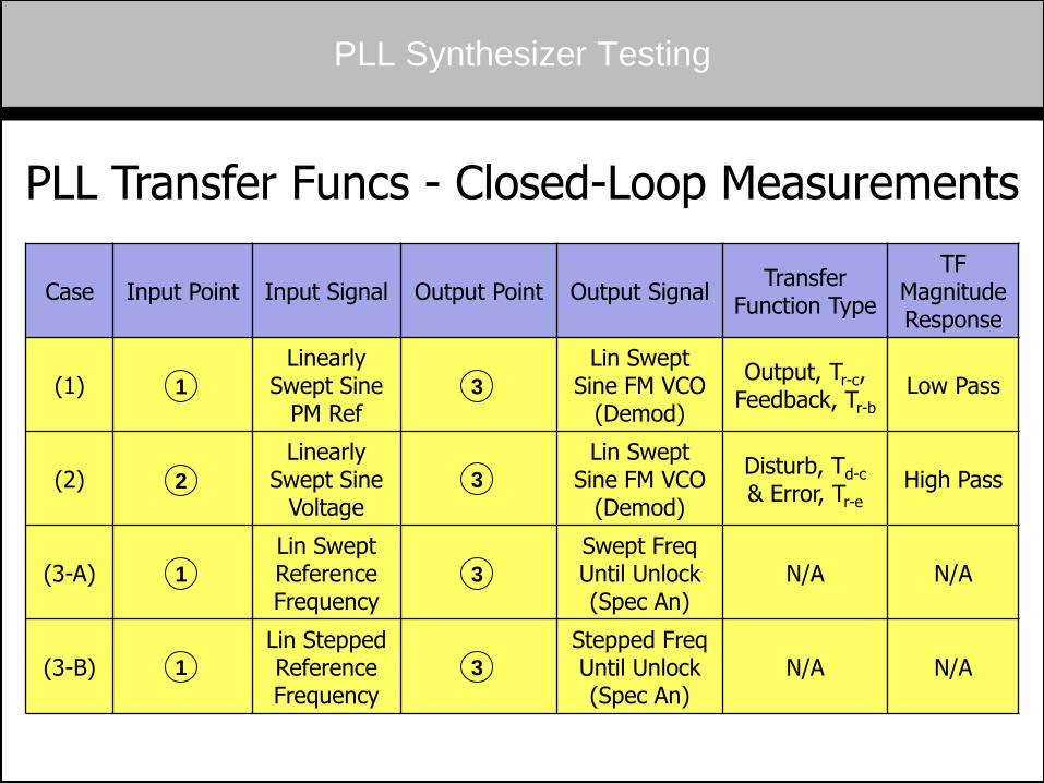
PLL Synthesizer Testing
PLL Transfer Funcs - Closed-Loop Measurements
Case Input Point Input Signal Output Point Output Signal Transfer
Function Type
TF Magnitude Response
(1) Linearly
Swept Sine PM Ref
Lin Swept Sine FM VCO
(Demod)
Output, Tr-c, Feedback, Tr-b
Low Pass
(2) Linearly
Swept Sine Voltage
Lin Swept Sine FM VCO
(Demod)
Disturb, Td-c
& Error, Tr-e High Pass
(3-A) Lin Swept Reference Frequency
Swept Freq Until Unlock (Spec An)
N/A N/A
(3-B) Lin Stepped Reference Frequency
Stepped Freq Until Unlock (Spec An)
N/A N/A
1
1
1
2
3
3
3
3
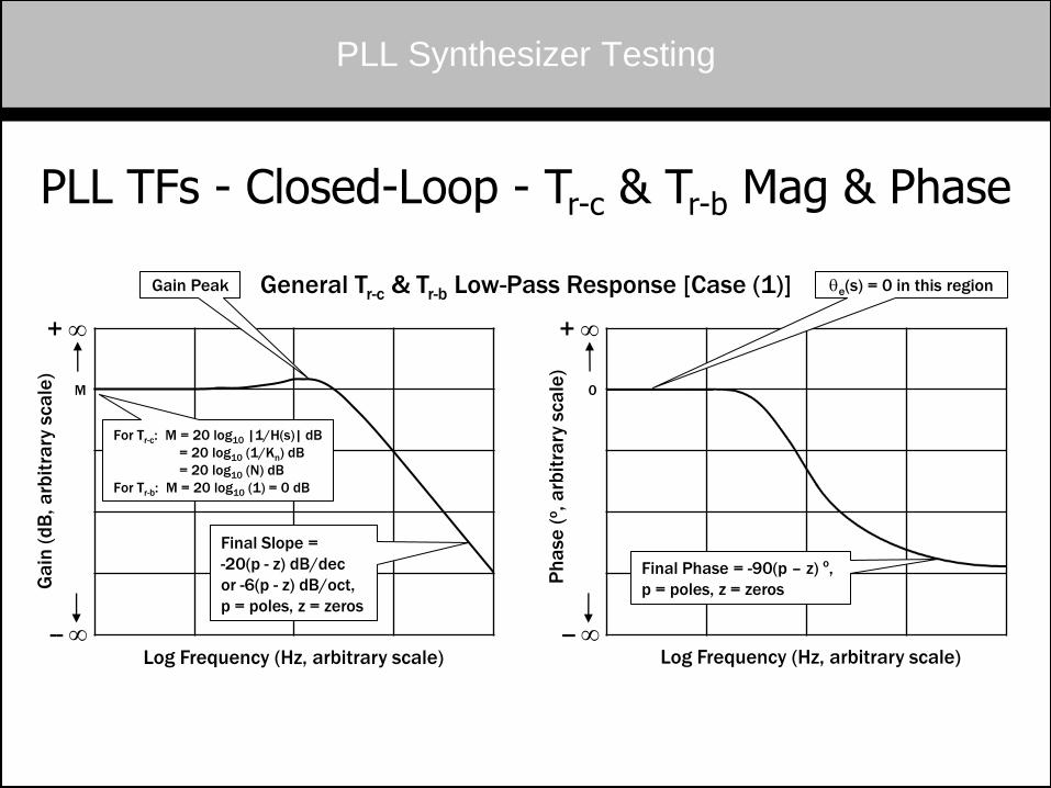
PLL Synthesizer Testing
PLL TFs - Closed-Loop - Tr-c & Tr-b Mag & Phase
Ph
ase
(o, a
rbit
rary
sca
le)
Ga
in (
dB
, a
rbit
rary
sca
le)
Log Frequency (Hz, arbitrary scale) Log Frequency (Hz, arbitrary scale) --
0
+
--
M
+
General Tr-c & Tr-b Low-Pass Response [Case (1)] qe(s) = 0 in this region Gain Peak
For Tr-c: M = 20 log10 |1/H(s)| dB
= 20 log10 (1/Kn) dB
= 20 log10 (N) dB
For Tr-b: M = 20 log10 (1) = 0 dB
Final Slope =
-20(p - z) dB/dec
or -6(p - z) dB/oct,
p = poles, z = zeros
Final Phase = -90(p – z) o,
p = poles, z = zeros
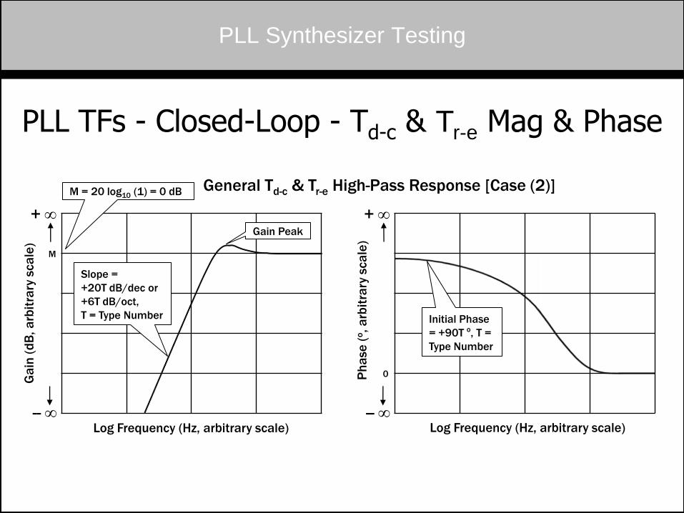
PLL Synthesizer Testing
PLL TFs - Closed-Loop - Td-c & Tr-e Mag & Phase
Ga
in (
dB
, a
rbit
rary
sca
le)
Ph
ase
(o, a
rbit
rary
sca
le)
Log Frequency (Hz, arbitrary scale) Log Frequency (Hz, arbitrary scale) --
0
+
--
M
+
General Td-c & Tr-e High-Pass Response [Case (2)]
Gain Peak
M = 20 log10 (1) = 0 dB
Slope =
+20T dB/dec or
+6T dB/oct,
T = Type Number Initial Phase
= +90T o, T =
Type Number
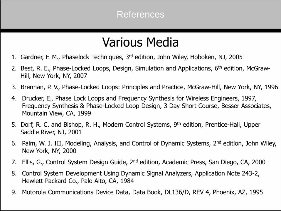
References
Various Media
1. Gardner, F. M., Phaselock Techniques, 3rd edition, John Wiley, Hoboken, NJ, 2005
2. Best, R. E., Phase-Locked Loops, Design, Simulation and Applications, 6th edition, McGraw-Hill, New York, NY, 2007
3. Brennan, P. V., Phase-Locked Loops: Principles and Practice, McGraw-Hill, New York, NY, 1996
4. Drucker, E., Phase Lock Loops and Frequency Synthesis for Wireless Engineers, 1997, Frequency Synthesis & Phase-Locked Loop Design, 3 Day Short Course, Besser Associates, Mountain View, CA, 1999
5. Dorf, R. C. and Bishop, R. H., Modern Control Systems, 9th edition, Prentice-Hall, Upper Saddle River, NJ, 2001
6. Palm, W. J. III, Modeling, Analysis, and Control of Dynamic Systems, 2nd edition, John Wiley, New York, NY, 2000
7. Ellis, G., Control System Design Guide, 2nd edition, Academic Press, San Diego, CA, 2000
8. Control System Development Using Dynamic Signal Analyzers, Application Note 243-2, Hewlett-Packard Co., Palo Alto, CA, 1984
9. Motorola Communications Device Data, Data Book, DL136/D, REV 4, Phoenix, AZ, 1995

Questions - Comments