Embed Size (px)
DESCRIPTION
pioneer manual
Citation preview
PIONEER CORPORATION 4-1, Meguro 1-chome,PIONEER ELECTRONICS (USA) INC. P.O. Box 1760, LonPIONEER EUROPE NV Haven 1087, Keetberglaan 1, 912PIONEER ELECTRONICS ASIACENTRE PTE. LTD. 253
PIONEER CORPORATION 2004
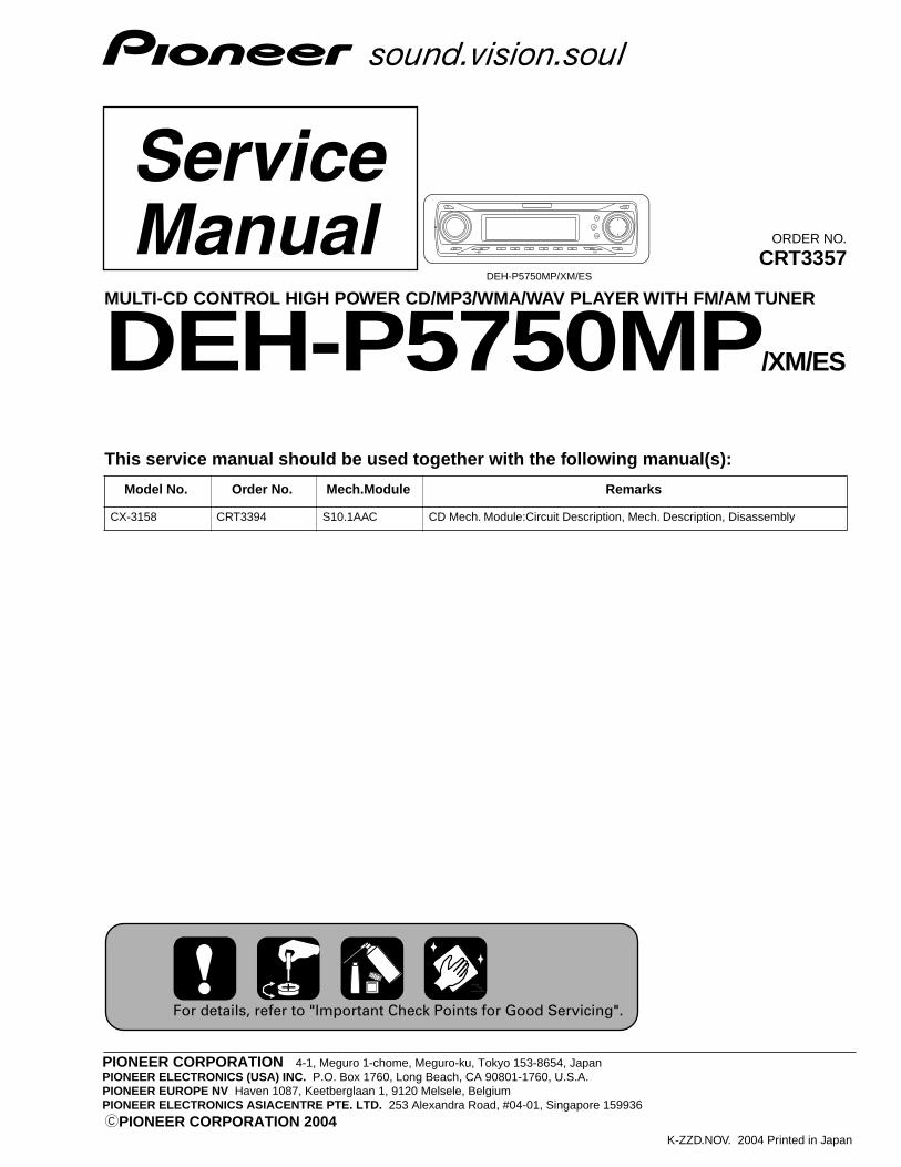
DEH-P5750MP/XM/ES
Meguro-ku, Tokyo 153-8654, Japang Beach, CA 90801-1760, U.S.A.
0 Melsele, BelgiumAlexandra Road, #04-01, Singapore 159936
ORDER NO.
CRT3357
MULTI-CD CONTROL HIGH POWER CD/MP3/WMA/WAV PLAYER WITH FM/AM TUNER
DEH-P5750MP/XM/ES
This service manual should be used together with the following manual(s):
Model No. Order No. Mech.Module Remarks
CX-3158 CRT3394 S10.1AAC CD Mech. Module:Circuit Description, Mech. Description, Disassembly
For details, refer to "Important Check Points for Good Servicing".
K-ZZD.NOV. 2004 Printed in Japan
C
D
F
A
B
E
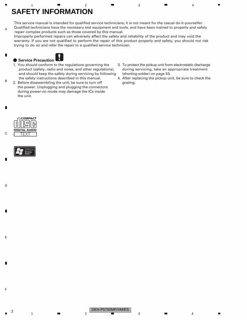
1 2 3 4SAFETY INFORMATIONThis service manual is intended for qualified service technicians; it is not meant for the casual do-it-yourselfer.Qualified technicians have the necessary test equipment and tools, and have been trained to properly and safely
complex products such as those covered by this manual.Improperly performed repairs can adversely affect the safety and reliability of the product and may void the
If you are not qualified to perform the repair of this product properly and safely, you should not risk and refer the repair to a qualified service technician.
repair
warranty.trying to do so
- Service Precaution1. You should conform to the regulations governing the
product (safety, radio and noise, and other regulations), and should keep the safety during servicing by following the safety instructions described in this manual.
2. Before disassembling the unit, be sure to turn off the power. Unplugging and plugging the connectors during power-on mode may damage the ICs inside the unit.
3. To protect the pickup unit from electrostatic discharge during servicing, take an appropriate treatment (shorting-solder) on page 53.
4. After replacing the pickup unit, be sure to check the grating.
DEH-P5750MP/XM/ES21 2 3 4
C
D
F
A
B
E
5 6 7 8
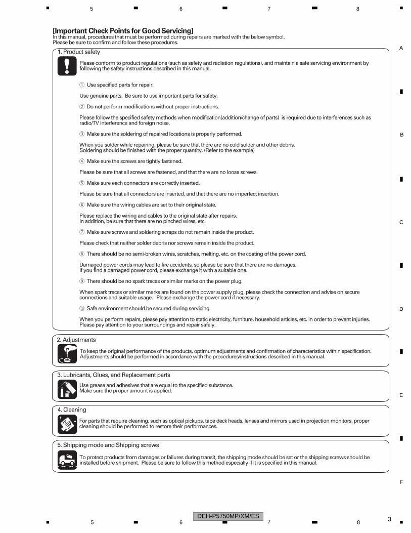
[Important Check Points for Good Servicing]In this manual, procedures that must be performed during repairs are marked with the below symbol.Please be sure to confirm and follow these procedures.
1. Product safety
Please conform to product regulations (such as safety and radiation regulations), and maintain a safe servicing environment by following the safety instructions described in this manual.
1 Use specified parts for repair.
Use genuine parts. Be sure to use important parts for safety.
2 Do not perform modifications without proper instructions.
Please follow the specified safety methods when modification(addition/change of parts) is required due to interferences such as radio/TV interference and foreign noise.
3 Make sure the soldering of repaired locations is properly performed.
When you solder while repairing, please be sure that there are no cold solder and other debris.Soldering should be finished with the proper quantity. (Refer to the example)
4 Make sure the screws are tightly fastened.
Please be sure that all screws are fastened, and that there are no loose screws.
5 Make sure each connectors are correctly inserted.
Please be sure that all connectors are inserted, and that there are no imperfect insertion.
6 Make sure the wiring cables are set to their original state.
Please replace the wiring and cables to the original state after repairs.In addition, be sure that there are no pinched wires, etc.
7 Make sure screws and soldering scraps do not remain inside the product.
Please check that neither solder debris nor screws remain inside the product.
8 There should be no semi-broken wires, scratches, melting, etc. on the coating of the power cord.
Damaged power cords may lead to fire accidents, so please be sure that there are no damages.If you find a damaged power cord, please exchange it with a suitable one.
9 There should be no spark traces or similar marks on the power plug.
When spark traces or similar marks are found on the power supply plug, please check the connection and advise on secure connections and suitable usage. Please exchange the power cord if necessary.
0 Safe environment should be secured during servicing.
When you perform repairs, please pay attention to static electricity, furniture, household articles, etc. in order to prevent injuries. Please pay attention to your surroundings and repair safely.
2. Adjustments
To keep the original performance of the products, optimum adjustments and confirmation of characteristics within specification.Adjustments should be performed in accordance with the procedures/instructions described in this manual.
4. Cleaning
For parts that require cleaning, such as optical pickups, tape deck heads, lenses and mirrors used in projection monitors, proper cleaning should be performed to restore their performances.
3. Lubricants, Glues, and Replacement parts
Use grease and adhesives that are equal to the specified substance. Make sure the proper amount is applied.
5. Shipping mode and Shipping screws
To protect products from damages or failures during transit, the shipping mode should be set or the shipping screws should be installed before shipment. Please be sure to follow this method especially if it is specified in this manual.
DEH-P5750MP/XM/ES 35 6 7 8
C
D
F
A
B
E
1 2 3 4
CONTENTS SAFETY INFORMATION..................................................................................................................................... 21. SPECIFICATIONS ............................................................................................................................................ 52. EXPLODED VIEWS AND PARTS LIST ............................................................................................................ 6
2.1 PACKING ................................................................................................................................................... 62.2 EXTERIOR................................................................................................................................................. 82.3 CD MECHANISM MODULE..................................................................................................................... 10
3. BLOCK DIAGRAM AND SCHEMATIC DIAGRAM.......................................................................................... 123.1 BLOCK DIAGRAM ................................................................................................................................... 123.2 OVERALL CONNECTION DIAGRAM(GUIDE PAGE).............................................................................. 143.3 KEYBOARD UNIT.................................................................................................................................... 203.4 CD MECHANISM MODULE(GUIDE PAGE) ............................................................................................ 22
4. PCB CONNECTION DIAGRAM ..................................................................................................................... 324.1 TUNER AMP ASSY ................................................................................................................................. 324.2 KEYBOARD UNIT.................................................................................................................................... 364.3 CD MECHAMODULE UNIT ..................................................................................................................... 384.4 PANEL UNIT ............................................................................................................................................ 40
5. ELECTRICAL PARTS LIST ............................................................................................................................ 416. ADJUSTMENT ............................................................................................................................................... 47
6.1 CD ADJUSTMENT................................................................................................................................... 476.2 CHECKING THE GRATING AFTER CHANGING THE PICKUP UNIT .................................................... 496.3 ERROR MODE ........................................................................................................................................ 516.4 SYSTEM MICROCOMPUTER TEST PROGRAM ................................................................................... 52
7. GENERAL INFORMATION............................................................................................................................. 537.1 DIAGNOSIS ............................................................................................................................................. 537.1.1 DISASSEMBLY ..................................................................................................................................... 537.1.2 CONNECTOR FUNCTION DESCRIPTION.......................................................................................... 567.2 PARTS...................................................................................................................................................... 577.2.1 IC .......................................................................................................................................................... 577.2.2 DISPLAY ............................................................................................................................................... 657.3 OPERATIONAL FLOW CHART ............................................................................................................... 667.4 CLEANING............................................................................................................................................... 67
8. OPERATIONS ................................................................................................................................................ 68
DEH-P5750MP/XM/ES41 2 3 4
C
D
F
A
B
E
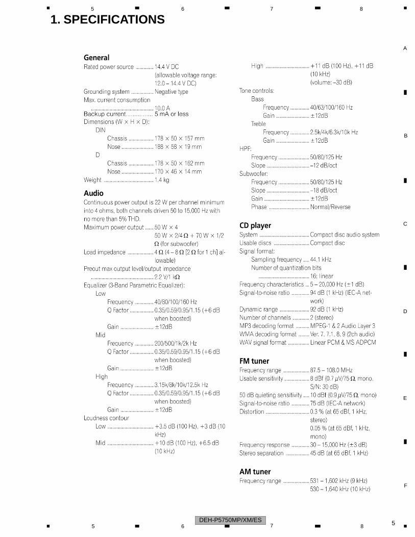
5 6 7 81. SPECIFICATIONS
DEH-P5750MP/XM/ES 55 6 7 8
C
D
F
A
B
E
1 2 3 4
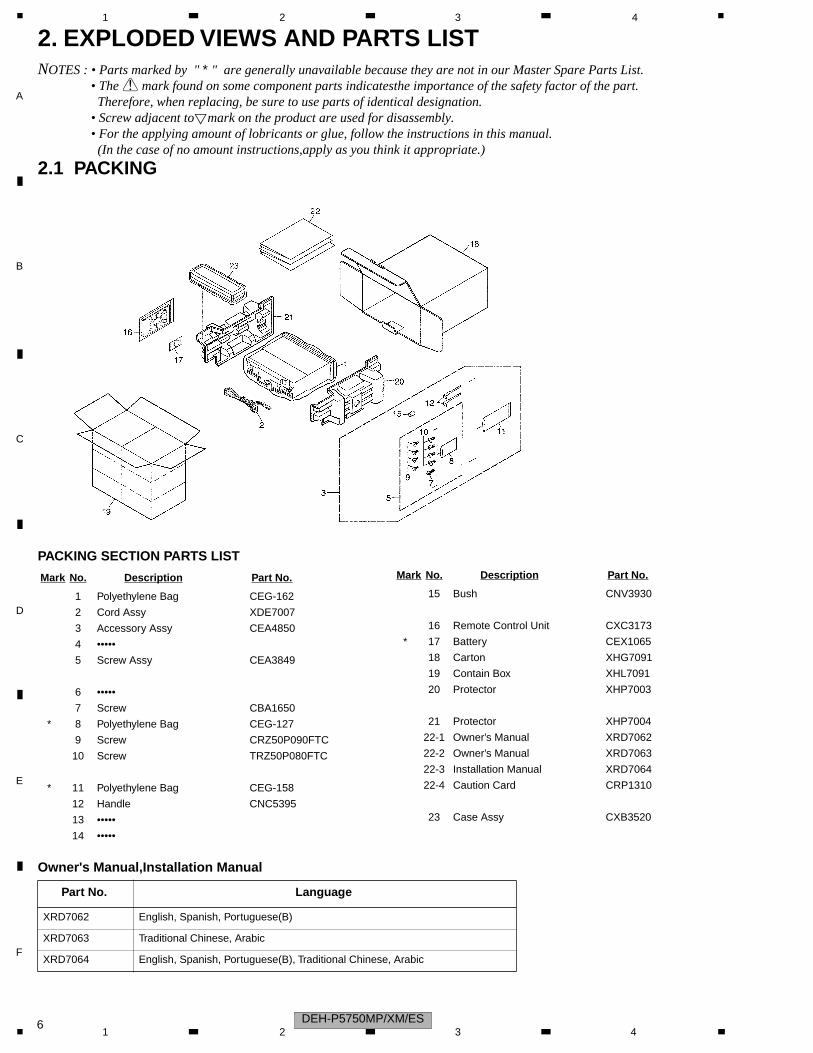
2. EXPLODED VIEWS AND PARTS LIST
2.1 PACKING
PACKING SECTION PARTS LIST
Owner's Manual,Installation Manual
NOTES : • Parts marked by " * " are generally unavailable because they are not in our Master Spare Parts List. • The > mark found on some component parts indicatesthe importance of the safety factor of the part. Therefore, when replacing, be sure to use parts of identical designation.
• Screw adjacent to mark on the product are used for disassembly.• For the applying amount of lobricants or glue, follow the instructions in this manual. (In the case of no amount instructions,apply as you think it appropriate.)
"
Mark No. Description Part No.
1 Polyethylene Bag CEG-162
2 Cord Assy XDE7007
3 Accessory Assy CEA4850
4 •••••
5 Screw Assy CEA3849
6 •••••
7 Screw CBA1650
* 8 Polyethylene Bag CEG-127
9 Screw CRZ50P090FTC
10 Screw TRZ50P080FTC
* 11 Polyethylene Bag CEG-158
12 Handle CNC5395
13 •••••
14 •••••
15 Bush CNV3930
16 Remote Control Unit CXC3173
* 17 Battery CEX1065
18 Carton XHG7091
19 Contain Box XHL7091
20 Protector XHP7003
21 Protector XHP7004
22-1 Owner’s Manual XRD7062
22-2 Owner’s Manual XRD7063
22-3 Installation Manual XRD7064
22-4 Caution Card CRP1310
23 Case Assy CXB3520
Mark No. Description Part No.
Part No. Language
XRD7062 English, Spanish, Portuguese(B)
XRD7063 Traditional Chinese, Arabic
XRD7064 English, Spanish, Portuguese(B), Traditional Chinese, Arabic
DEH-P5750MP/XM/ES61 2 3 4

C
D
F
A
B
E
5 6 7 8
DEH-P5750MP/XM/ES 75 6 7 8
C
D
F
A
B
E
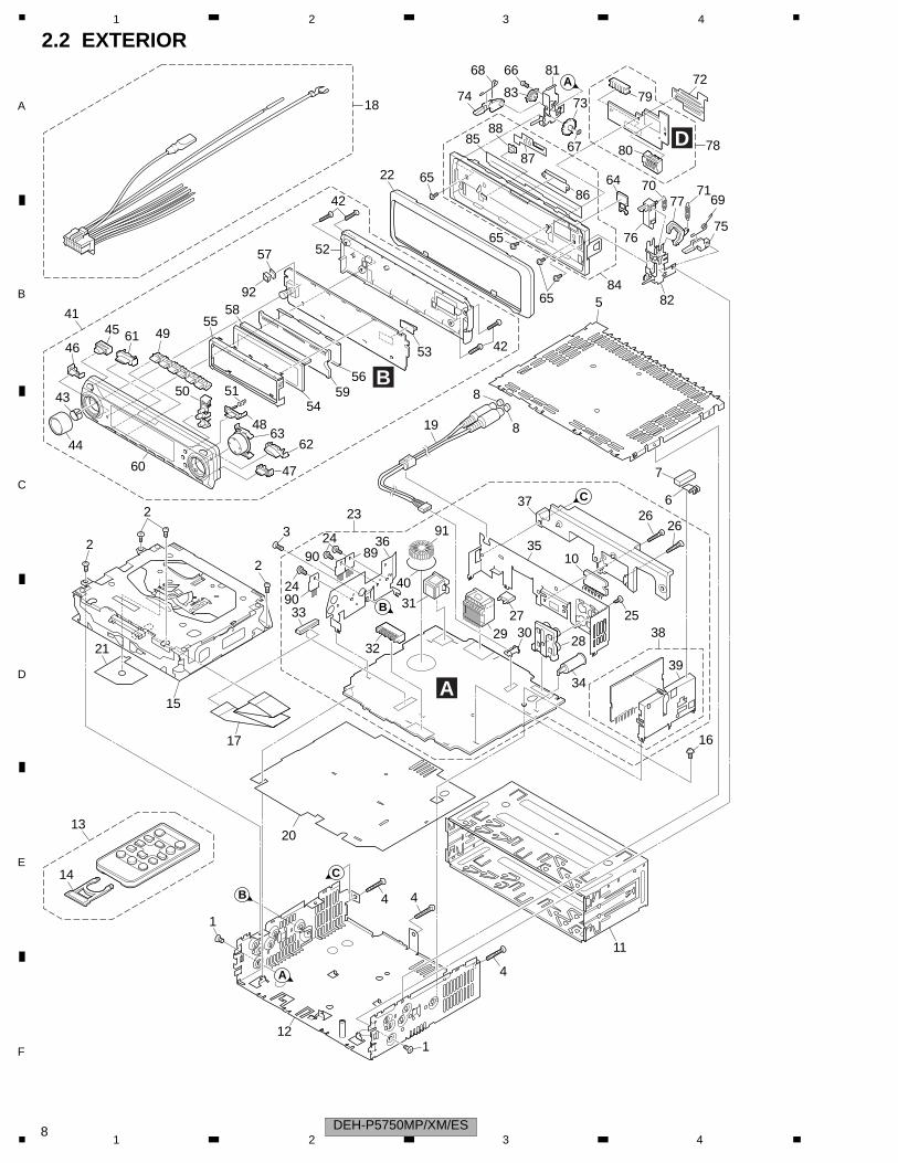
1 2 3 42.2 EXTERIOR
A
A
B
B
C
C
1874
68 66
83
87
8885
86
81
73
78
7077
7169
7972
8067
64
7675
82584
65
65
6522
42
42
5257
9258
55496145
46
43
44
60 47
6263
48
5154
5956
53
19
23
3691
33
32
24
24
90
90 892
2
2
15
21
17
2013
14
12
4
1
1
4
4
3
8
7
6
850
41
40
31
2927
35
3726
26
25
28
10
30
34
16
11
38
39
A
B
D
DEH-P5750MP/XM/ES81 2 3 4
C
D
F
A
B
E
5 6 7 8
EXTERIOR SECTION PARTS LIST
Mark No. Description Part No.
1 Screw BMZ30P040FZK
2 Screw BSZ26P060FTC
3 Screw BSZ30P060FTC
4 Screw BSZ30P200FTC
5 Case CNB2793
6 Earth Plate CNC8915
7 Cushion CNM8890
8 Cap CNV6727
9 •••••
10 IC(IC301) PAL007A
11 Holder Unit CXB6681
12 Chassis Unit CXB9528
13 Remote Control Unit CXC3173
14 Cover CNS7068
15 CD Mechanism Module(S10.1AACA) CXK5668
16 Screw ISS26P055FTC
17 Cable XDE7002
18 Cord Assy XDE7007
19 Cord Assy XDE7009
20 Insulator XNM7100
21 Insulator XNM7106
22 Panel XNS7088
23 Tuner Amp Assy XWM7091
24 Screw ASZ26P060FTC
25 Screw BPZ26P080FTC
26 Screw BSZ26P160FTC
> 27 Fuse(10A) CEK1208
28 Pin Jack(CN352) CKB1051
29 Plug(CN901) CKM1376
30 Plug(CN351) CKS1238
31 Connector(CN101) CKS3408
32 Plug(CN801) CKS3537
33 Connector(CN651) CKS3837
34 Antenna Jack(CN401) CKX1056
35 Holder CND1239
36 Holder CND1352
37 Heat Sink CNR1668
38 FM/AM Tuner Unit CWE1802
39 Holder CND2144
40 Insulator XNM7031
41 Detachable Assy XXA7281
42 Screw BPZ20P100FZK
43 Spring CBL1470
44 Knob XAA7021
45 Button(CLK) XAC7062
46 Button(DISP) XAC7063
47 Button(SW) XAC7064
48 Button(OPEN) XAC7065
49 Button(1-6) XAC7070
50 Button(F,A,EQ) XAC7071
51 Spring XBH7001
52 Cover XNS7087
53 Connector(CN1800) CKS4524
54 LCD XAW7013
55 Holder XNC7008
56 Sheet XNM7044
57 Cushion XNM7049
58 Connector XNV7020
59 Lighting Conductor XNV7021
60 Sub Grille Assy XXA7290
61 Button Unit(SRC) XXA7307
62 Button Unit(BAND) XXA7308
63 Sub Button Assy XXA7310
64 Button(EJECT) CAC7752
65 Screw(M2x4.5) CBA1647
66 Screw(M2x4) CBA1649
67 Washer CBF1038
68 Spring CBH2650
69 Spring CBH2651
70 Spring CBH2652
71 Spring CBH2653
72 Holder CND1254
73 Gear CNV5997
74 Arm CNV7400
75 Arm CNV7401
76 Arm CNV7402
77 Arm CNV7403
78 Panel Unit CWM8758
79 Socket(CN1950) CKS3550
80 Connector(CN1951) CKS4806
81 Holder Unit CXB9501
82 Holder Unit CXB9502
83 Damper Unit CXB9503
84 Sub Panel Unit XXA7361
85 Cover CNM6854
86 Lighting Conductor CNV6487
87 Spring CBL1512
88 Pin CNV6486
89 IC(IC901) NJM2388F84
90 Transistor(Q650,911) 2SD2396
91 Choke Coil(L901) CTH1280
92 IC(IC1802) TSOP4840SB1
Mark No. Description Part No.
DEH-P5750MP/XM/ES 95 6 7 8
C
D
F
A
B
E
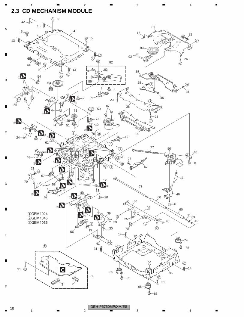
1 2 3 42.3 CD MECHANISM MODULE
A
D
H
L
M
NO
Q
R
A
B
C
D
E
F
GH
I
J
K
LM
N
O
Q
B
16
25
13 83
42
68
28
82
4
71
23
J
K
38
23
59
87
86
5
13
34
5
5
13
44
5C
52
53
36
4
73
29
51
18
64
76
50
10
72
75
49
77
67
27
78
60
9048
8
17
46
6
60
1189
43
70
14
31
65
85
66
85
31
35
14
74
85
1
23
R
91
12
33
61
63
21
79
57
58
6280
13
4
86
I
45
28
724
47
P
41
20
40
69
39
30P
1956
F
E22
81
15
G
26
5
54
37
55
93
92
10
C
1GEM10242GEM10453GEM1035
1
1
1
1
1
1
1
1
2
2
2
2
1
1
1
1
1
2
2
1
3
DEH-P5750MP/XM/ES101 2 3 4
C
D
F
A
B
E
5 6 7 8
CD MECHANISM MODULE SECTION PARTS LIST
Mark No. Description Part No.
1 CD Core Unit(S10.1) CWX3096
2 Connector(CN101) CKS4182
3 Connector(CN901) CKS4017
4 Screw BMZ20P035FTC
5 Screw BSZ20P040FTC
6 Screw(M2x4) CBA1362
7 Screw(M2x3) CBA1824
8 Screw(M2x3) CBA1825
9 •••••
10 Washer CBF1038
11 Washer CBF1060
12 Spring CBH2390
13 Spring CBH2606
14 Spring CBH2607
15 Spring CBH2608
16 Spring CBH2609
17 Spring CBH2610
18 Spring CBH2735
19 Spring CBH2612
20 Spring CBH2613
21 Spring CBH2614
22 Spring CBH2615
23 Spring CBH2616
24 Spring CBH2617
25 Spring CBH2620
26 Spring CBH2621
27 Spring CBH2641
28 Spring CBH2642
29 Spring CBH2643
30 Spring CBH2659
31 Spring CBH2688
32 •••••
33 Shaft CLA4441
34 Frame CNC9962
35 Frame CNC9963
36 Bracket CND2712
37 Bracket CND1895
38 Arm CNC9968
39 Arm CND1909
40 Lever CND2032
41 Lever CNC9984
42 Sheet CNM8134
43 Collar CNV7798
44 Guide CNV7799
45 Arm CNV8403
46 Rack CNV8374
47 Holder CNV8376
48 Holder CNV8377
49 Arm CNV8378
50 Gear CNV8379
51 Gear CNV8380
52 Gear CNV8381
53 Gear CNV8382
54 Gear CNV8383
55 Gear CNV8384
56 Rack CNV8385
57 Arm CNV8386
58 Arm CNV8387
59 Guide CNV8388
60 Roller CNV7218
61 Gear CNV8389
62 Arm CNV8391
63 Arm CNV8390
64 Arm CNV8392
65 Damper CNV7313
66 Damper CNV7314
67 Arm CNV8394
68 Arm CNV8395
69 Guide CNV8396
70 Guide CNV8397
71 Holder CNV8398
72 Arm CNV8402
73 Gear CNV8400
74 Damper CNV7618
75 Motor Unit(M1) CXC4440
76 Chassis Unit CXC2318
77 Screw Unit CXB8729
78 Gear Unit CXC2397
79 Arm Unit CXC2316
80 Arm CND1896
81 Arm CND1894
82 Motor Unit(M2) CXB8933
83 Bracket CNC9985
84 •••••
85 Screw(M2x5) EBA1028
86 Screw JFZ20P020FTC
87 Screw JGZ17P022FTC
88 •••••
89 Washer YE20FTC
90 Pickup Unit(P10)(Service) CXX1641
91 Screw IMS26P030FTC
92 Spring CBL1635
93 Clamper CNV8372
Mark No. Description Part No.
DEH-P5750MP/XM/ES 115 6 7 8
C
D
F
A
B
E
S
IN2L41
IN4L+43
IN4L-44
IN3L42
ELECTSOUR
Q831
S802
W
NJ
7
LEV
Q821
Q840
Q832
C
Q
Q841
B.UP
POWER
ROL
C
MUTE20
1 2 3 4
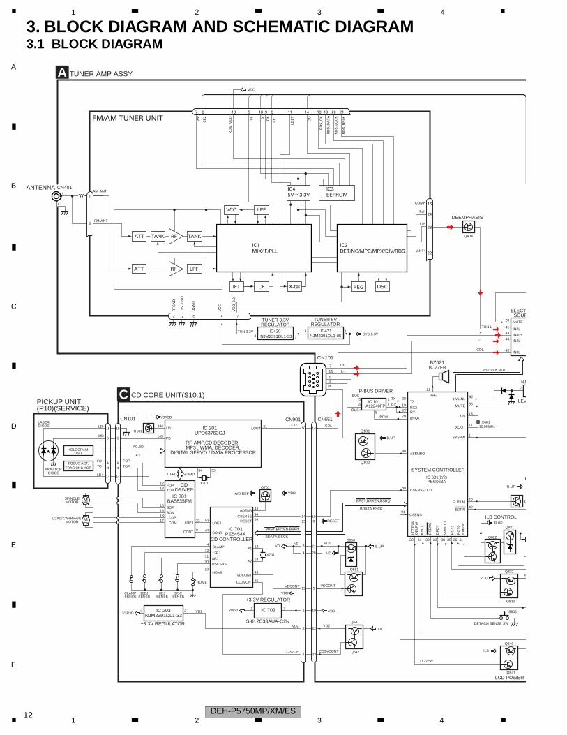
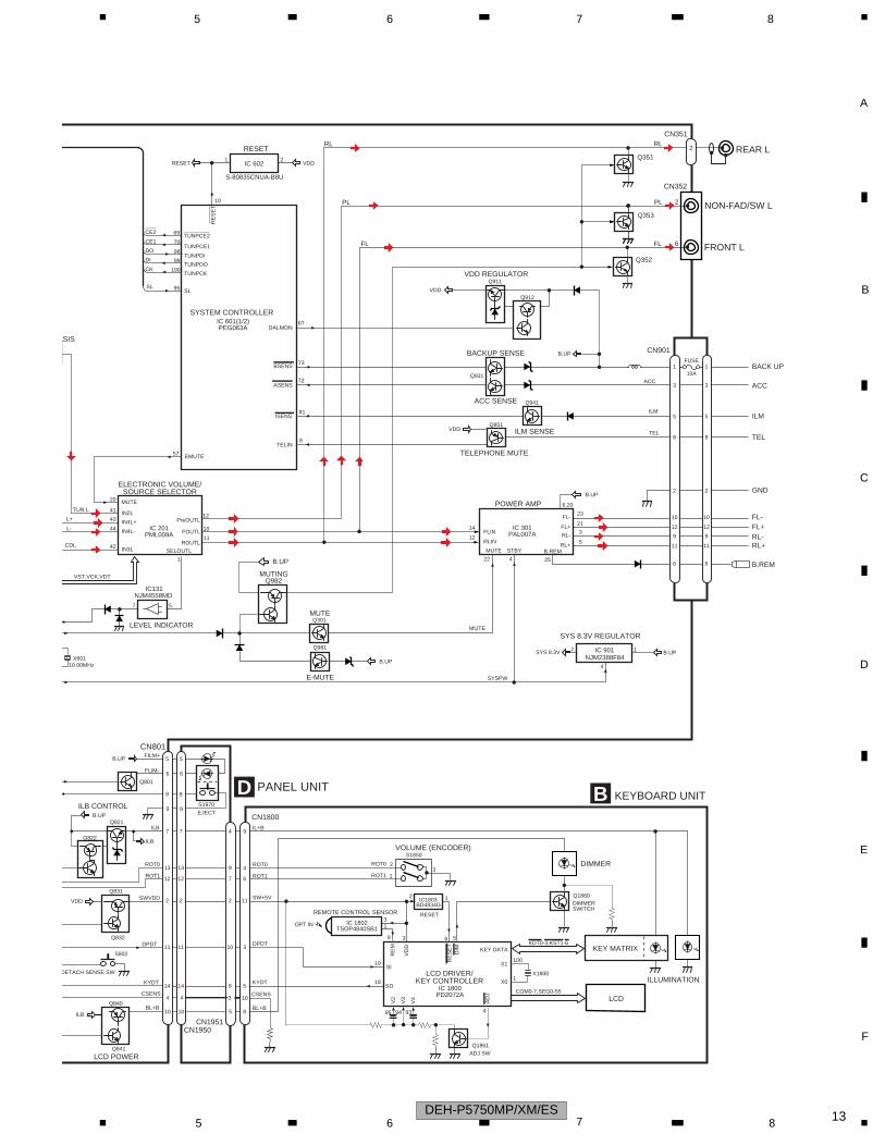
3. BLOCK DIAGRAM AND SCHEMATIC DIAGRAM3.1 BLOCK DIAGRAM
BRST,BRXEN,BSRQ
C
CN901
Q101
M
LASERDIODE
MONITORDIODE
CLAMPSENSE
DISC SENSE
FOCUS ACT.
SPINDLEMOTOR
MCARRIAGEMOTOR
LOAD/
TRACKING ACT.
LD-
MD
FO+
TO+
15
5
14
PICKUP UNIT(P10)(SERVICE)
HOLOGRAM UNIT
IC 301BA5835FM
IC 201UPD63763GJ
IC 703
+3.3V REGULATOR
RF-AMP,CD DECODER, MP3 , WMA, DECODER,
DIGITAL SERVO / DATA PROCESSOR
CDDRIVER
3VD
VD
3VDD
10L-OUT
5
CN101
TOP
FOP
16SOP
15SOM
18LCOP
17LCOM
22
2
LOEJ
31LOUT
9CONT
12FOP
TD/FD
AC,BD
F,E
SD/MD
3
13TOP
HOME
12EJSENSE
8EJSENSE
LD+ 14
142LD
143PD
CD CORE UNIT(S10.1)
3534
X201
12EJ
CONT
LOEJ
HOME
32
97
53
47
VDD
IC 203NJM2391DL1-33
+3.3V REGULATOR
V3R3D23
CD3VON 46
VDCONT49
S-812C33AUA-C2N
CD CONTROLLER
IC 701PE5454A
94CSENSE
4
V3R3D
19
1
BDATA,BSCK
VD22
Q701
43ADENA
VDD
15
5
14
14
CLAMP4
VD2
VDCONT
1CD3VON
13
12
X701
X1
X28EJ
31
DSCSNS30
A/D REF
CDL
VD1
VDCONT
VD2
14RESET1415
ASENBO
85MUTE
XIN
XOUT
PEE
22
38
80
28
19
79
SYSTEM CONTROLLER
IC 601(2/2)PEG063A
CN4011
2
BUS-
BUS+
L+
L-
TX
RX2
IPPW
SW
VD
D
B.UP
CN651
Q651
Q650
TUNER AMP ASSY
13
X60111
VST,VCK,VDT
TUN L
CDL
33
DP
DT
34
KY
DT
1SYSPW
41
ILM
PW
DETACH SENSE S
39
DS
EN
S
A
5
81
7
CN101
11BUZZER
20
19
5
14
21
IC 101HA12240FP
IP-BUS DRIVER
1
2
8
6
5 TX
RX
IPPW
B.UP
Q101
Q102
NJM2391DL1-33IC420 13
SYS 8.3VTUN 3.3V
TUNER 3.3VREGULATOR
VDD
ANTENNA
92LVLINL
B.UP
Q82220
LCD
PW
/O
ELP
W
ILB
BZ621
35
RO
T1
36
RO
T0
VDD
VDD
BRST,BRXEN,BSRQ
BDATA,BSCK EJTIN42
FLPILM40
VD22
VD
Q642
Q641
23
NJM2391DL1-05IC421
3 1
TUNER 5VREGULATOR
Q404
DEEMPHASIS
L+
L-
CD3VCONT
LCDPW
CSENS
LCD
ILB CONT
10.00MHz
91
27 RX
910
CSENSEOUT56
RESET
FM ANT
RFG
ND
OS
CG
ND
DG
ND
VC
C
VD
D_3
.3
WC
CE
2
RO
M_V
DD SL DI
CK
CE
1
LDE
T
DO
RD
S_C
K
RD
S_D
AT
A
RD
S_L
OC
K
RD
S_H
SLK
7 13 5 10 8 11 14 18 19 20 21
1
3
2 12 15 4 17
AM ANT
16
23
COMP
Lch
24Rch
22ANT1
6 9
IC45V 3.3V
IC3EEPROM
IC2DET/NC/MPC/MPX/DIV/RDS
REG OSCX-talCFIFT
LPF
TANK
RF
RFTANK
ATT
ATT
LPFVCO
IC1MIX/IF/PLL
←
FM/AM TUNER UNIT
DEH-P5750MP/XM/ES121 2 3 4
C
D
F
A
B
E
L+
L-
X601
VST,VC
TUN L
CDL
DETACH SEN
B
Q822
ILB
VDD
ASIS
L
ILB C
10.00MHz
5 6 7 8
10
1
BSENS
ASENS
VDD
B.UP
72
73
10FOUTL11
ROUTL
ILB
SWVDD
23
21
3
5
FL-
FL+
RL-
RL+
ACC
IN2L41
IN4L+43
IN4L-44
IN3L42
FLIN14
RLIN12
22 4
RESET
POWER AMP
IC 601(1/2)PEG063A
IC 201PML009A
IC 602
IC 301PAL007A
VDD
Q911
Q931
SYSPW
ELECTRONIC VOLUME/SOURCE SELECTOR
STBYMUTE
Q831
2
K,VDT
DPDT
KYDT
SYS 8.3V B.UP
Q301MUTE
PL
FL
Q352
12PreOUTL
7
2
11
14
7
2
11
14
CN1950CN1951
4
2
10
8
PANEL UNIT
MUTING
S802
SE SW
SYSTEM CONTROLLER
Q951VDD
TELIN8
25
B.REM
VDD REGULATOR
BACKUP SENSE
ACC SENSE
TELEPHONE MUTE
SYS 8.3V REGULATOR
3
9
11
12
10
1
8
6
3
9
11
12
10
1
8
6
2 2
D
CN901
Q982
B.UP
FUSE
10A
SL
TUNPCE1
TUNPDI
TUNPDO
95
69
70
98
99
TUNPCK100
CE1
DO
DI
CK
Q912
DALMON67
B.UP
6,20
Q981
10 10 5
Q353
PL
FL
Q941
ISENS81
ILM SENSE
5 5
NJM4558MDIC131
57
1
SELOUTL
LEVEL INDICATOR
.UPQ821
ILB
Q840
13 13 9
12 12 7ROT1
ROT0
Q832
S-80835CNUA-B8U
NON-FAD/SW L
FRONT L
8 8
S1970
EJECT9 9
5
6
5
6
CN801
Q801
RL
Q351
CN351RL
REAR L
FL-FL+RL-RL+
BACK UP
GND
ACC
B.REM
ILM
TEL
Q841
CN352
TUNPCE2CE2
RE
SE
T
B.UP
12
NJM2388F84IC 901
4
SL
2
BL+B
B.UP FILM+
FLIM-
E-MUTE
MUTE
ILM
TEL
4 4 3
CD POWER
ONTROL
CSENS
EMUTE57
MUTE20
RESET
2
6
IL+B
SW+5V
IC 1800PD2072A
LCD DRIVER/KEY CONTROLLER
KEY MATRIX
9
11
KEY DATA
VD
D
3
CN1800
KEYBOARD UNIT
3
5
DPDT
KYDT
IC 1802TSOP4840SB1
REMOTE CONTROL SENSOR
OPT IN31
9
RE
M
19
18
SI
SO
LCD
B
DIM
6
8BL+B
Q1860
DIMMER
5
ILLUMINATION
X1
X0
100
X18001
S1850
32
1
4
6 ROT1
ROT0
ROT1
ROT0
VOLUME (ENCODER)
Q1861
493
V4
AD
J
KDT0-3,KST1-6
IC1803BD4834G
RE
SE
T
12
RESET
COM0-7,SEG0-55
DIMMERSWITCH
ADJ SW
CSENS10
94
V3
95
V2
DEH-P5750MP/XM/ES 135 6 7 8
C
D
F
A
B
E
SYSTEM
1 2 3 4
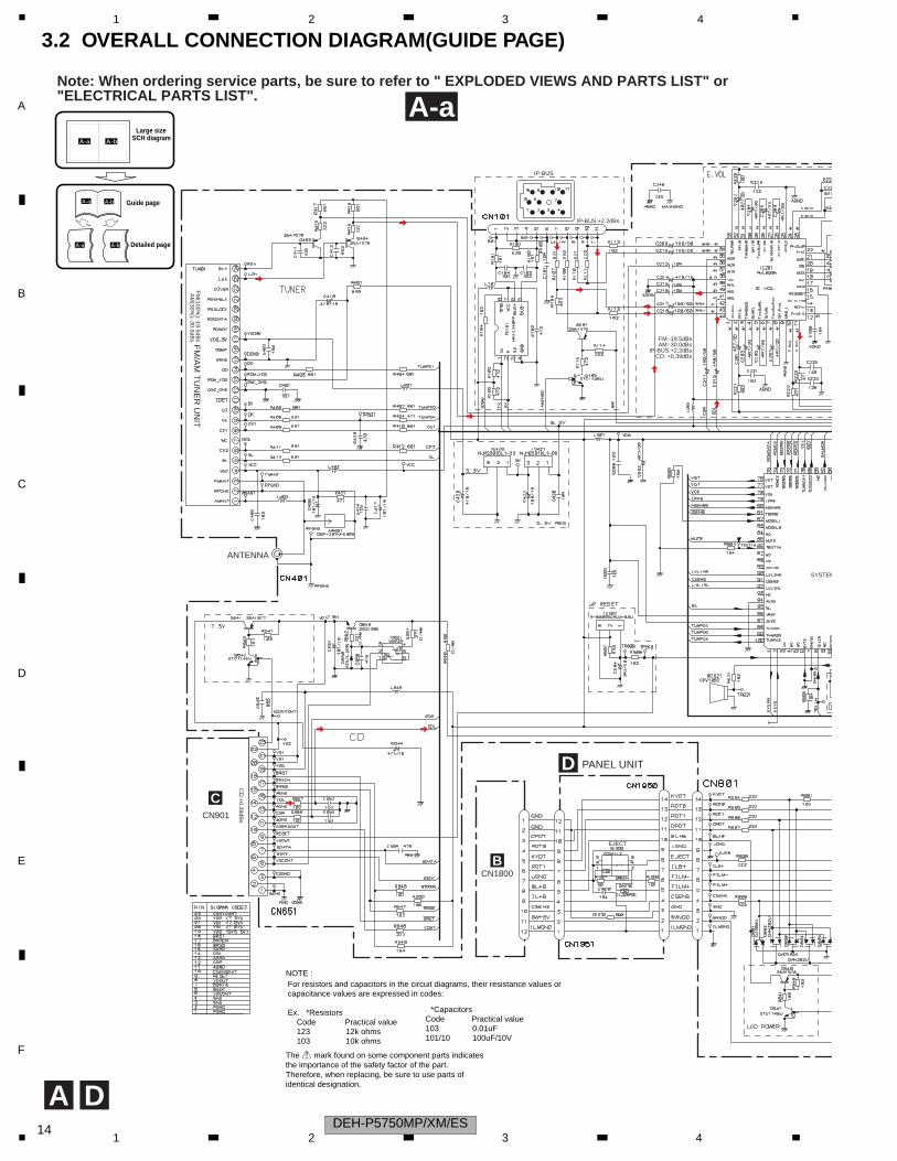
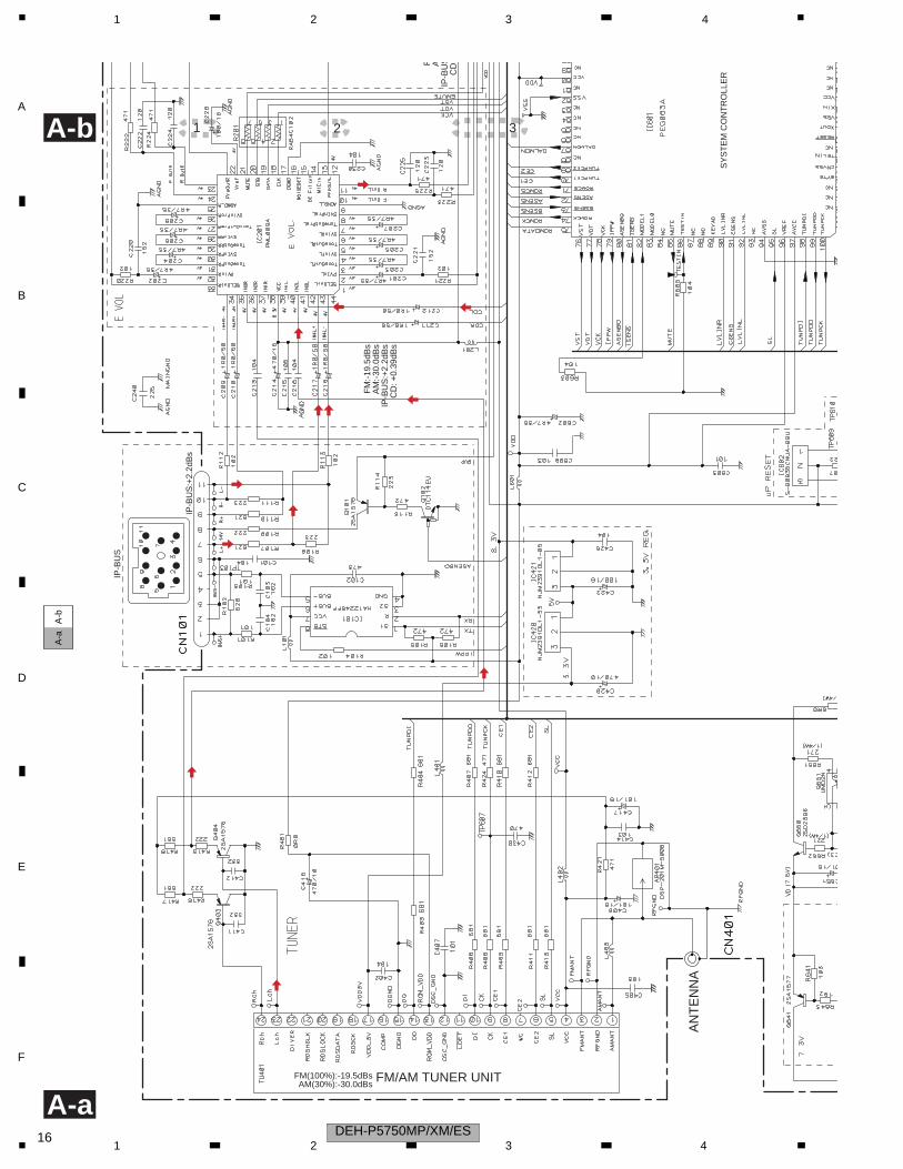
3.2 OVERALL CONNECTION DIAGRAM(GUIDE PAGE)
A-a A-b
A-a A-b
A-b A-a
Large sizeSCH diagram
Guide page
Detailed page
Note: When ordering service parts, be sure to refer to " EXPLODED VIEWS AND PARTS LIST" or "ELECTRICAL PARTS LIST". A-a
A D
The > mark found on some component parts indicatesthe importance of the safety factor of the part.Therefore, when replacing, be sure to use parts ofidentical designation.
B
D PANEL UNIT
FM
/AM
TU
NE
R U
NIT
CCN901
ANTENNA
CN1800
EJECT
IP-BUS
For resistors and capacitors in the circuit diagrams, their resistance values orcapacitance values are expressed in codes:
Ex. *Resistors Code Practical value 123 12k ohms 103 10k ohms
*Capacitors Code Practical value 103 0.01uF 101/10 100uF/10V
NOTE :
FM
(100%):-19.5dB
sA
M(30%
):-30.0dBs
IP-BUS:+2.2dBs
CD
:+0.39dB
s
FM:-19.5dBsAM:-30.0dBs
IP-BUS:+2.2dBsCD: +0.39dBs
DEH-P5750MP/XM/ES141 2 3 4
C
D
F
A
B
E
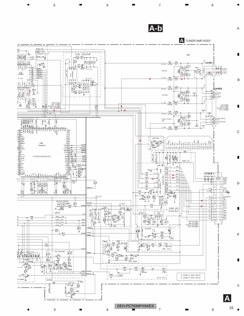
A-a A-b
A-a A-b
A-b A-a
5 6 7 8
A-b
A
3A
BACK UP
10A
>FUSE
CEK1208
>
A TUNER AMP ASSY
SUB WOOFERR ch
SUB WOOFERL ch
FRONTR ch
FRONTL ch
REARR ch
REARL ch
DETACH SENSE
PO
WE
R A
MP
SYSTEM CONTROLLER
FM:+5.6dBsAM: -4.9dBs
IP-BUS:+10.3dBsCD:+10.49dBs
FM:+31.6dBsAM:+21.1dBs
IP-BUS:+36.3dBsCD:+36.49dBs
FM:4.8dBsAM:-5.7dBs
IP-BUS:+8.5dBsCD: +9.2dBs
DEH-P5750MP/XM/ES 155 6 7 8
C
D
F
A
B
E
1 2 3 4
1 2 3
A-a
A-b
A-a
A-a
A-b
FM/AM TUNER UNIT
AN
TE
NN
A
IP-B
US
SY
ST
EM
CO
NT
RO
LLE
R
FM(100%):-19.5dBsAM(30%):-30.0dBs
IP-B
US
:+2.
2dB
s
FM
:-19
.5dB
sA
M:-
30.0
dBs
IP-B
US
:+2.
2dB
sC
D: +
0.39
dBs
F AIP
-BU
SC
D
DEH-P5750MP/XM/ES161 2 3 4
C
D
F
A
B
E
5 6 7 8
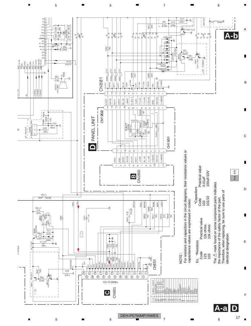
4 5 6 7
A-a
A-b
A-a
A-a
A-b
D
The
> m
ark
foun
d on
som
e co
mpo
nent
par
ts in
dica
tes
the
impo
rtan
ce o
f the
saf
ety
fact
or o
f the
par
t.T
here
fore
, whe
n re
plac
ing,
be
sure
to u
se p
arts
of
iden
tical
des
igna
tion.
B
DP
AN
EL
UN
IT
CC
N90
1
CN
1800
EJE
CT
For
res
isto
rs a
nd c
apac
itors
in th
e ci
rcui
t dia
gram
s, th
eir
resi
stan
ce v
alue
s or
capa
cita
nce
valu
es a
re e
xpre
ssed
in c
odes
:
Ex.
*R
esis
tors
C
ode
Pra
ctic
al v
alue
1
23
12k
ohm
s
103
1
0k o
hms
*C
apac
itors
C
ode
P
ract
ical
val
ue
103
0.
01uF
1
01/1
0
100u
F/1
0V
NO
TE
:
CD:+0.39dBs
DEH-P5750MP/XM/ES 175 6 7 8
C
D
F
A
B
E
> FUSE
MP
1 2 3 4
1 2 3
A-a
A-b
A-b
3A
>
AT
UN
ER
AM
P A
SS
Y
SU
B W
OO
FE
RR
ch
SU
B W
OO
FE
RL
ch
FR
ON
TR
ch
FR
ON
TL
ch
RE
AR
R c
h
RE
AR
L ch
EM
CO
NT
RO
LLE
R
FM
:+5.
6dB
sA
M: -
4.9d
Bs
IP-B
US
:+10
.3dB
sC
D:+
10.4
9dB
s
FM
:4.8
dBs
AM
:-5.
7dB
sIP
-BU
S:+
8.5d
Bs
CD
: +9.
2dB
s
DEH-P5750MP/XM/ES181 2 3 4
C
D
F
A
B
E
5 6 7 8
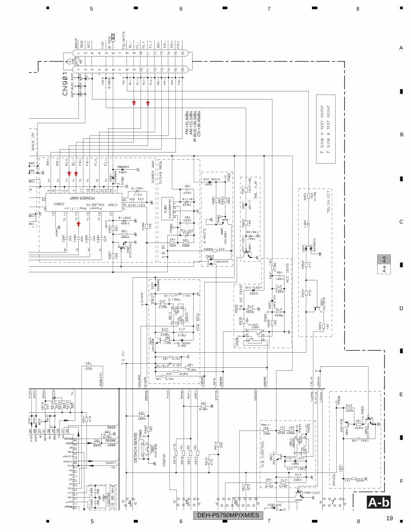
4 5 6 7
A-a
A-b
A-b
BACK
UP
10A
> FUSE
CEK1
208
DE
TAC
H S
EN
SE
POWER AMP
FM
:+31
.6dB
sA
M:+
21.1
dBs
IP-B
US
:+36
.3dB
sC
D:+
36.4
9dB
s
DEH-P5750MP/XM/ES 195 6 7 8
C
D
F
A
B
E
B
1 2 3 4
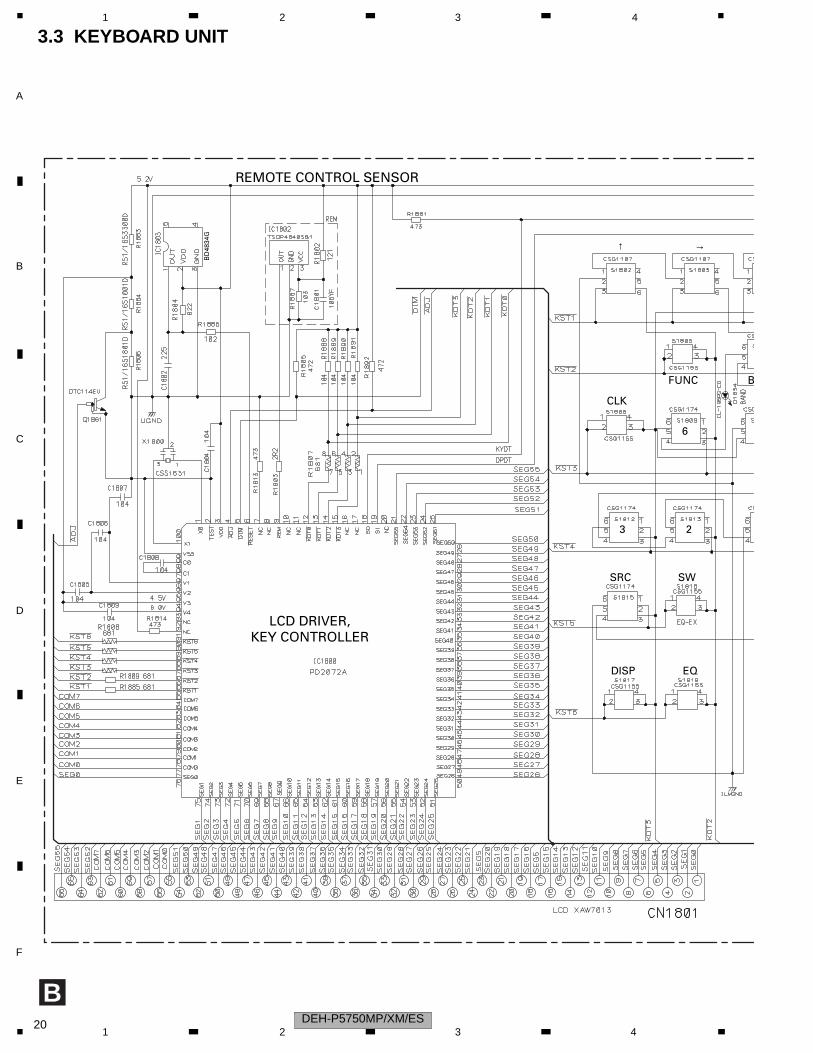
3.3 KEYBOARD UNIT
B
CLK
3 2
6
↑
FUNC
DISP
SWSRC
EQ
LCD DRIVER,KEY CONTROLLER
REMOTE CONTROL SENSOR
BD
4834
G
→
DEH-P5750MP/XM/ES201 2 3 4
C
D
F
A
B
E
2
6
UNC
SW
EQ
→
5 6 7 8
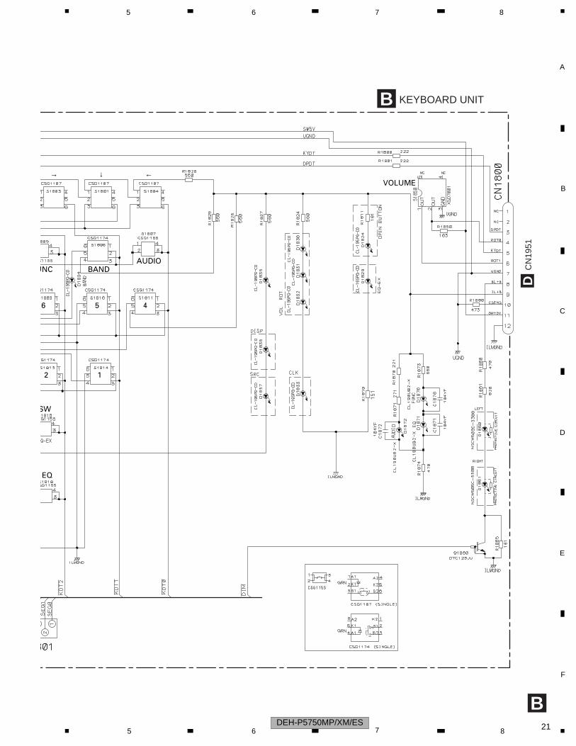
B
D
B KEYBOARD UNIT
CN
1951
1
BAND
5 4
AUDIO
←↓VOLUME
DEH-P5750MP/XM/ES 215 6 7 8
C
D
F
A
B
E
TY
1 2 3 4
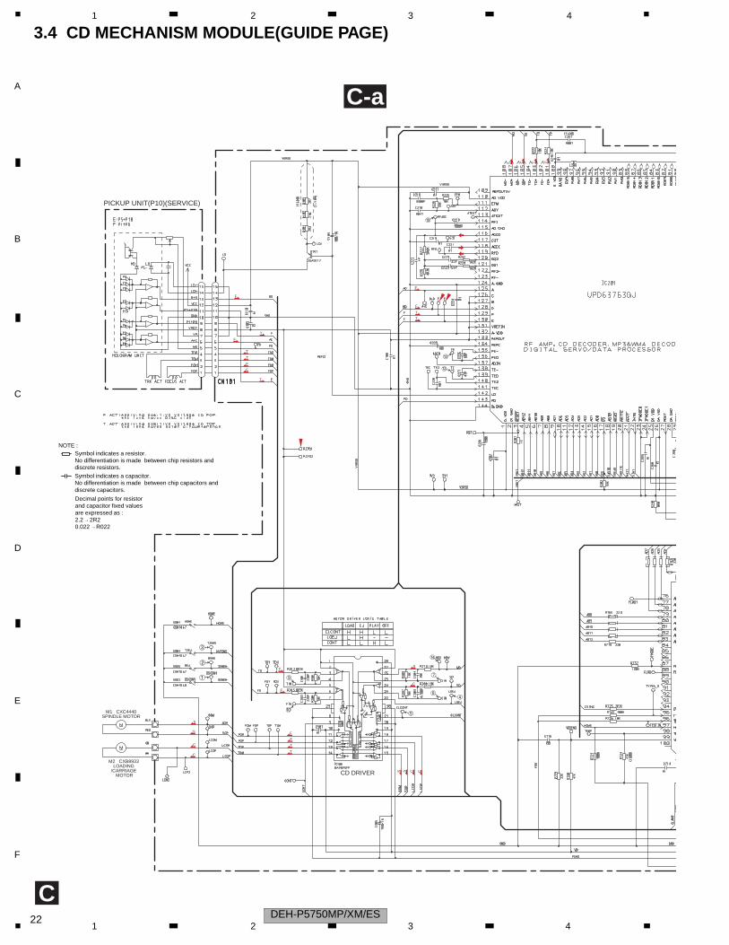
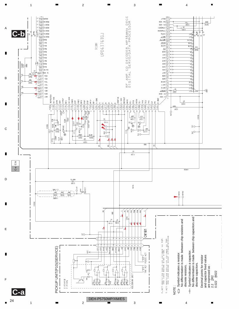
3.4 CD MECHANISM MODULE(GUIDE PAGE)
C-a
C
PICKUP UNIT(P10)(SERVICE)
M1 CXC4440SPINDLE MOTOR
M2 CXB8933LOADING
/CARRIAGE MOTOR CD DRIVER
T
F
F
T
T
T
F
F
FTCS
T
F
S
C
F
F
T
T
S S C C
C
C
S
S
T
T
F
F
1
3
2
0
9 7
$
8
5
4
@
#
%
Decimal points for resistorand capacitor fixed valuesare expressed as :2.2 2R20.022 R022
← ←
Symbol indicates a resistor.No differentiation is made between chip resistors anddiscrete resistors.
NOTE :
Symbol indicates a capacitor.No differentiation is made between chip capacitors anddiscrete capacitors.
DEH-P5750MP/XM/ES221 2 3 4
C
D
F
A
B
E
5 6 7 8
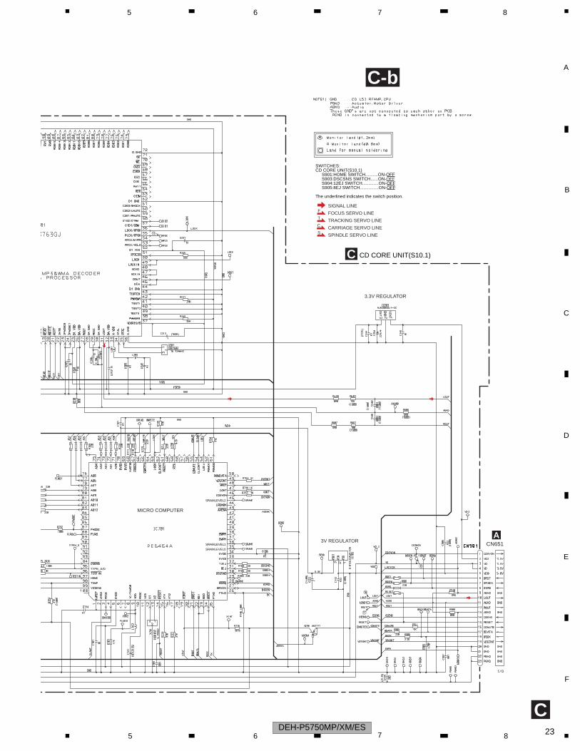
C-b
C
ras
SRAMLEVEL0
SRAMLEVEL1
SRAMLEVEL2
TYPE_A/D
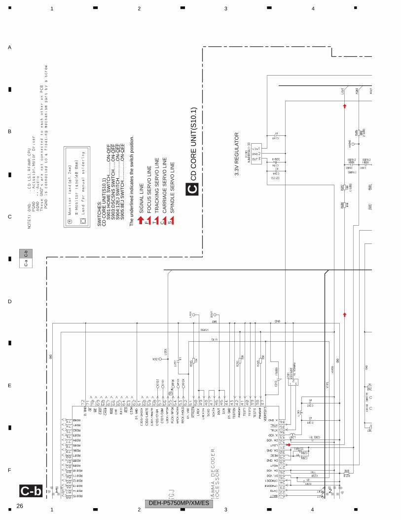
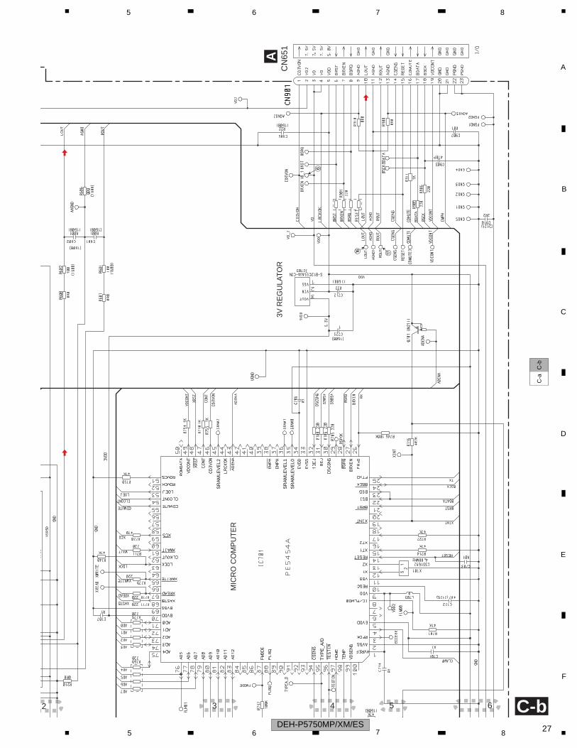
SWITCHES:CD CORE UNIT(S10.1) S901:HOME SWITCH..........ON-OFF S903:DSCSNS SWITCH......ON-OFF S904:12EJ SWITCH.............ON-OFF S905:8EJ SWITCH...............ON-OFF
The underlined indicates the switch position.
CD CORE UNIT(S10.1)C
ACN651
FSIGNAL LINE
FOCUS SERVO LINE
TRACKING SERVO LINE
CARRIAGE SERVO LINE
SPINDLE SERVO LINE
T
C
S
3V REGULATOR
3.3V REGULATOR
MICRO COMPUTER
!
^
&
6
DEH-P5750MP/XM/ES 235 6 7 8
C
D
F
A
B
E
2.2
2R
20.
022
R
022
←
←
1 2 3 4
A-a
C-b
C-a
C-a
C-b 1 2
PIC
KU
P U
NIT
(P10
)(S
ER
VIC
E)
Dec
imal
poi
nts
for
resi
stor
and
capa
cito
r fix
ed v
alue
sar
e ex
pres
sed
as :
Sym
bol i
ndic
ates
a r
esis
tor.
No
diffe
rent
iatio
n is
mad
e b
etw
een
chip
res
isto
rs a
nddi
scre
te r
esis
tors
.
NO
TE
: Sym
bol i
ndic
ates
a c
apac
itor.
No
diffe
rent
iatio
n is
mad
e b
etw
een
chip
cap
acito
rs a
nddi
scre
te c
apac
itors
.
T
F F
T
T TFF
F
T
C
S
T T F F@#
%
DEH-P5750MP/XM/ES241 2 3 4
C
D
F
A
B
E
2
Dec
imal
poi
nts
for
resi
stor
disc
rete
cap
acito
rs.
5 6 7 8
A-a
C-b
C-a
C-a
C-b3 4 5 6
M1
CX
C44
40S
PIN
DLE
MO
TO
R
M2
CX
B89
33LO
AD
ING
/CA
RR
IAG
E M
OT
OR
CD
DR
IVE
R
and
capa
cito
r fix
ed v
alue
sar
e ex
pres
sed
as :
2.2
2R
20.
022
R
022
←
←
T F
S C
F F T T
S
S
C
C
CCSS
13 2
097$ 8
5
4
DEH-P5750MP/XM/ES 255 6 7 8
C
D
F
A
B
E
1 2 3 4
C-a
C-b
C-b 1 2
ra
s
SW
ITC
HE
S:
CD
CO
RE
UN
IT(S
10.1
)
S90
1:H
OM
E S
WIT
CH
......
....O
N-O
FF
S
903:
DS
CS
NS
SW
ITC
H...
...O
N-O
FF
S
904:
12E
J S
WIT
CH
......
......
.ON
-OF
F
S90
5:8E
J S
WIT
CH
......
......
...O
N-O
FF
The
und
erlin
ed in
dica
tes
the
switc
h po
sitio
n.
CD
CO
RE
UN
IT(S
10.1
)C
FS
IGN
AL
LIN
E
FO
CU
S S
ER
VO
LIN
E
TR
AC
KIN
G S
ER
VO
LIN
E
CA
RR
IAG
E S
ER
VO
LIN
E
SP
IND
LE S
ER
VO
LIN
E
T C S
3.3V
RE
GU
LAT
OR
!
DEH-P5750MP/XM/ES261 2 3 4
C
D
F
A
B
E
2
5 6 7 8
C-a
C-b
C-b3 4 5 6
SR
AM
LEV
EL0
SR
AM
LEV
EL1
SR
AM
LEV
EL2
TY
PE
_A/D
AC
N65
13V
RE
GU
LAT
OR
MIC
RO
CO
MP
UT
ER
^ &
6
DEH-P5750MP/XM/ES 275 6 7 8
C
D
F
A
B
E
1 2 3 4
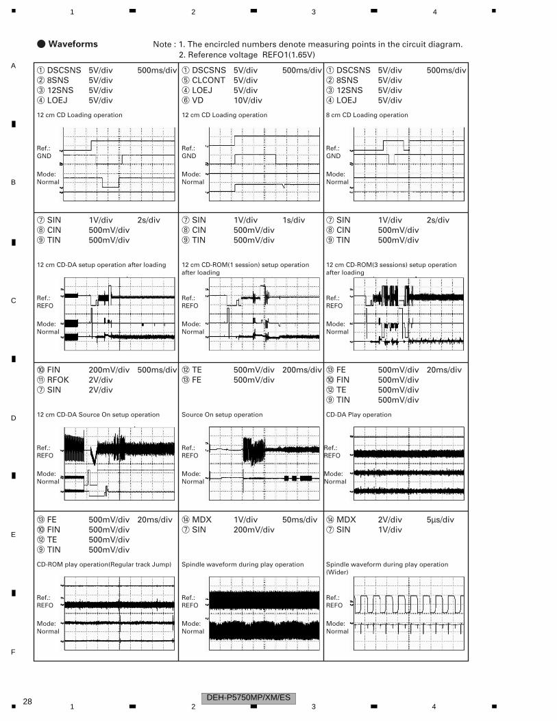
- Waveforms Note : 1. The encircled numbers denote measuring points in the circuit diagram.2. Reference voltage REFO1(1.65V)
1 DSCSNS2 8SNS3 12SNS4 LOEJ
5V/div5V/div5V/div5V/div
500ms/div
12 cm CD Loading operation
Ref.:GND
Mode:Normal
1 DSCSNS2 8SNS3 12SNS4 LOEJ
5V/div5V/div5V/div5V/div
500ms/div
Ref.:GND
Mode:Normal
1 DSCSNS5 CLCONT4 LOEJ6 VD
5V/div5V/div5V/div10V/div
500ms/div
12 cm CD Loading operation 8 cm CD Loading operation
Ref.:GND
Mode:Normal
0 FIN! RFOK7 SIN
200mV/div2V/div2V/div
500ms/div
12 cm CD-DA Source On setup operation
Ref.:REFO
Mode:Normal
# FE0 FIN@ TE9 TIN
500mV/div500mV/div500mV/div500mV/div
20ms/div
Ref.:REFO
Mode:Normal
@ TE# FE
500mV/div500mV/div
200ms/div
Source On setup operation CD-DA Play operation
Ref.:REFO
Mode:Normal
# FE0 FIN@ TE9 TIN
500mV/div500mV/div500mV/div500mV/div
20ms/div
CD-ROM play operation(Regular track Jump)
Ref.:REFO
Mode:Normal
$ MDX7 SIN
2V/div1V/div
5µs/div
Ref.:REFO
Mode:Normal
$ MDX7 SIN
1V/div200mV/div
50ms/div
Spindle waveform during play operation Spindle waveform during play operation(Wider)
Ref.:REFO
Mode:Normal
7 SIN8 CIN9 TIN
1V/div500mV/div500mV/div
2s/div
12 cm CD-DA setup operation after loading 12 cm CD-ROM(3 sessions) setup operation after loading
Ref.:REFO
Mode:Normal
7 SIN8 CIN9 TIN
1V/div500mV/div500mV/div
2s/div
Ref.:REFO
Mode:Normal
7 SIN8 CIN9 TIN
1V/div500mV/div500mV/div
1s/div
12 cm CD-ROM(1 session) setup operation after loading
Ref.:REFO
Mode:Normal
DEH-P5750MP/XM/ES281 2 3 4
C
D
F
A
B
E
5 6 7 8
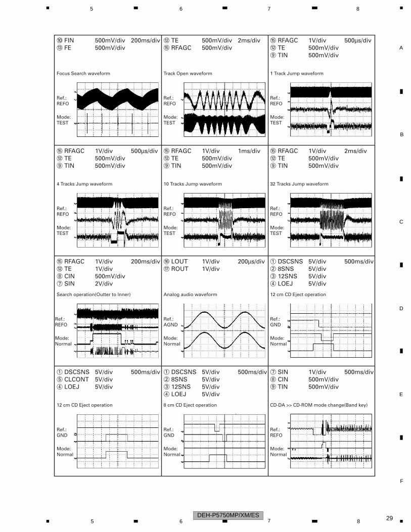
0 FIN# FE
500mV/div500mV/div
200ms/div
Focus Search waveform
Ref.:REFO
Mode:TEST
% RFAGC@ TE9 TIN
1V/div500mV/div500mV/div
500µs/div
Ref.:REFO
Mode:TEST
@ TE% RFAGC
500mV/div500mV/div
2ms/div
Track Open waveform 1 Track Jump waveform
Ref.:REFO
Mode:TEST
% RFAGC@ TE8 CIN7 SIN
1V/div1V/div500mV/div2V/div
200ms/div
Ref.:REFO
Mode:Normal
Search operation(Outter to Inner)
^ LOUT& ROUT
1V/div1V/div
200µs/div
Analog audio waveform
Ref.:AGND
Mode:Normal
7 SIN8 CIN9 TIN
1V/div500mV/div500mV/div
500ms/div
Ref.:REFO
Mode:Normal
1 DSCSNS2 8SNS3 12SNS4 LOEJ
5V/div5V/div5V/div5V/div
500ms/div
12 cm CD Eject operation
CD-DA >> CD-ROM mode change(Band key)
Ref.:GND
Mode:Normal
% RFAGC@ TE9 TIN
1V/div500mV/div500mV/div
500µs/div
4 Tracks Jump waveform 32 Tracks Jump waveform
Ref.:REFO
Mode:TEST
% RFAGC@ TE9 TIN
1V/div500mV/div500mV/div
2ms/div
Ref.:REFO
Mode:TEST
% RFAGC@ TE9 TIN
1V/div500mV/div500mV/div
1ms/div
10 Tracks Jump waveform
Ref.:REFO
Mode:TEST
1 DSCSNS5 CLCONT4 LOEJ
5V/div5V/div5V/div
500ms/div
12 cm CD Eject operation
Ref.:GND
Mode:Normal
1 DSCSNS2 8SNS3 12SNS4 LOEJ
5V/div5V/div5V/div5V/div
500ms/div
8 cm CD Eject operation
Ref.:GND
Mode:Normal
DEH-P5750MP/XM/ES 295 6 7 8
C
D
F
A
B
E
1 2 3 4
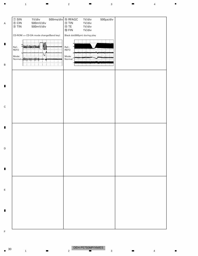
7 SIN8 CIN9 TIN
1V/div500mV/div500mV/div
500ms/div
CD-ROM >> CD-DA mode change(Band key)
Ref.:REFO
Mode:Normal
% RFAGC9 TIN@ TE0 FIN
1V/div1V/div1V/div1V/div
500µs/div
Black dot(800µm) during play
Ref.:REFO
Mode:Normal
DEH-P5750MP/XM/ES301 2 3 4

C
D
F
A
B
E
5 6 7 8
DEH-P5750MP/XM/ES 315 6 7 8
C
D
F
A
B
E
ORD
1 2 3 4
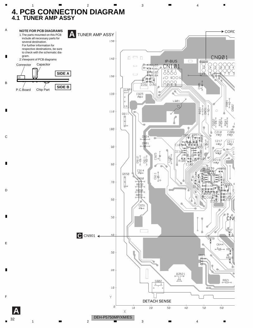
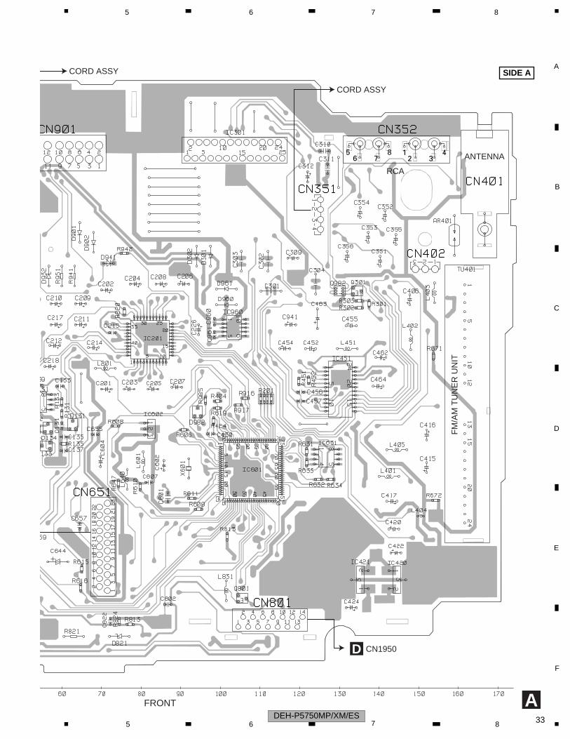
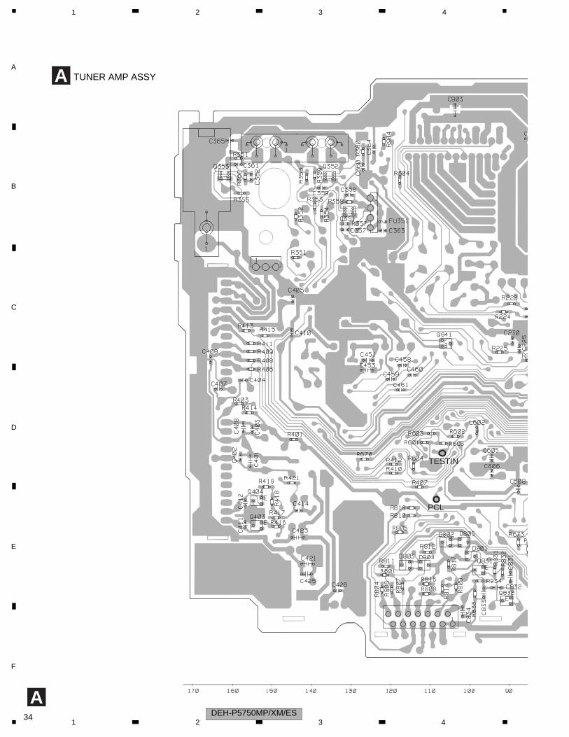
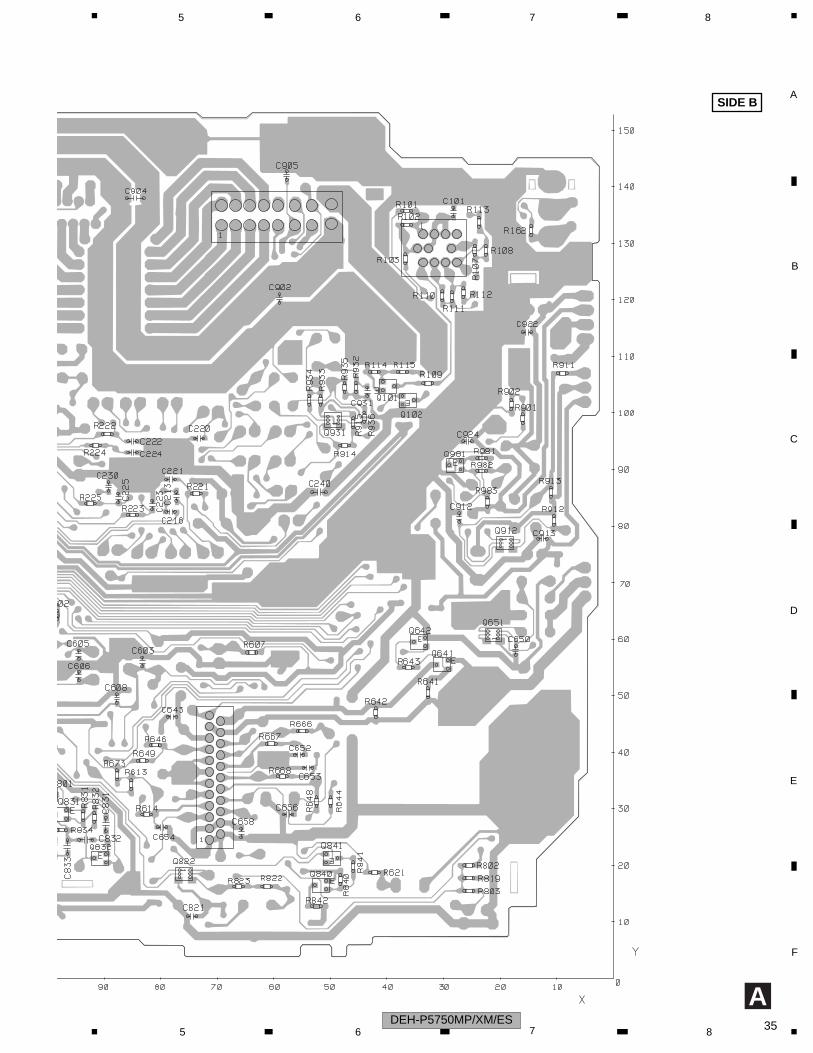
4. PCB CONNECTION DIAGRAM4.1 TUNER AMP ASSY
CapacitorConnector
P.C.Board Chip Part
A
A TUNER AMP ASSY
SIDE B
SIDE A
NOTE FOR PCB DIAGRAMS1.The parts mounted on this PCB include all necessary parts for several destination. For further information for respective destinations, be sure to check with the schematic dia- gram.2.Viewpoint of PCB diagrams IP-BUS
C CN901
C
DETACH SENSE
DEH-P5750MP/XM/ES321 2 3 4
C
D
F
A
B
E
5 6 7 8
A
SIDE A
D CN1950
FRONT
RCA
ANTENNA
FM
/AM
TU
NE
R U
NIT
12 3
456 7
8
CORD ASSY
CORD ASSY
DEH-P5750MP/XM/ES 335 6 7 8
C
D
F
A
B
E
1 2 3 4
A
A TUNER AMP ASSY
PCL
TESTIN
DEH-P5750MP/XM/ES341 2 3 4
C
D
F
A
B
E
5 6 7 8
A
SIDE B
DEH-P5750MP/XM/ES 355 6 7 8
C
D
F
A
B
E
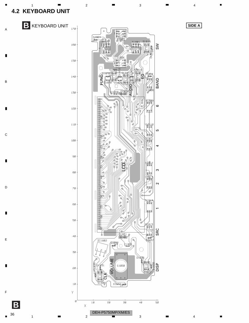
1 2 3 44.2 KEYBOARD UNIT
B
B KEYBOARD UNIT SIDE A
VO
LUM
E
DIS
PS
RC
EQ
CLK
12
34
56
SW
BA
ND
FUN
C
AU
DIO
LCD
↑
←
↓
→
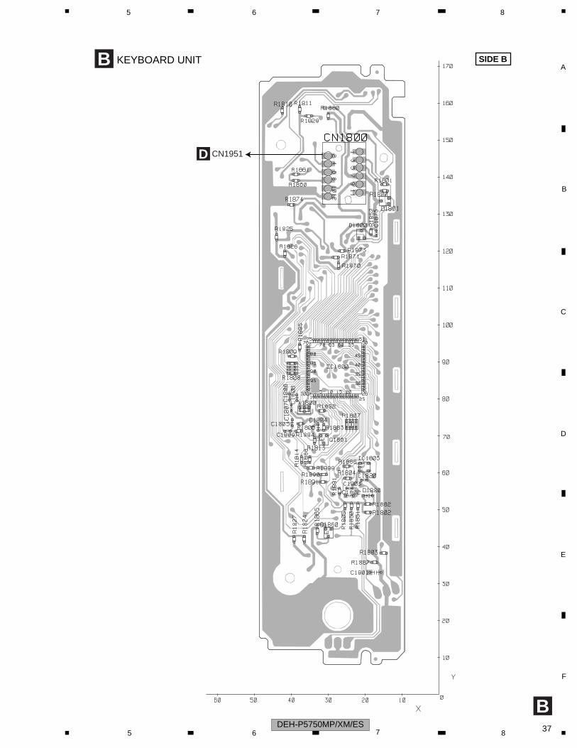
DEH-P5750MP/XM/ES361 2 3 4
C
D
F
A
B
E
5 6 7 8
B
B KEYBOARD UNIT SIDE B
D CN1951
DEH-P5750MP/XM/ES 375 6 7 8
C
D
F
A
B
E
1 2 3 4
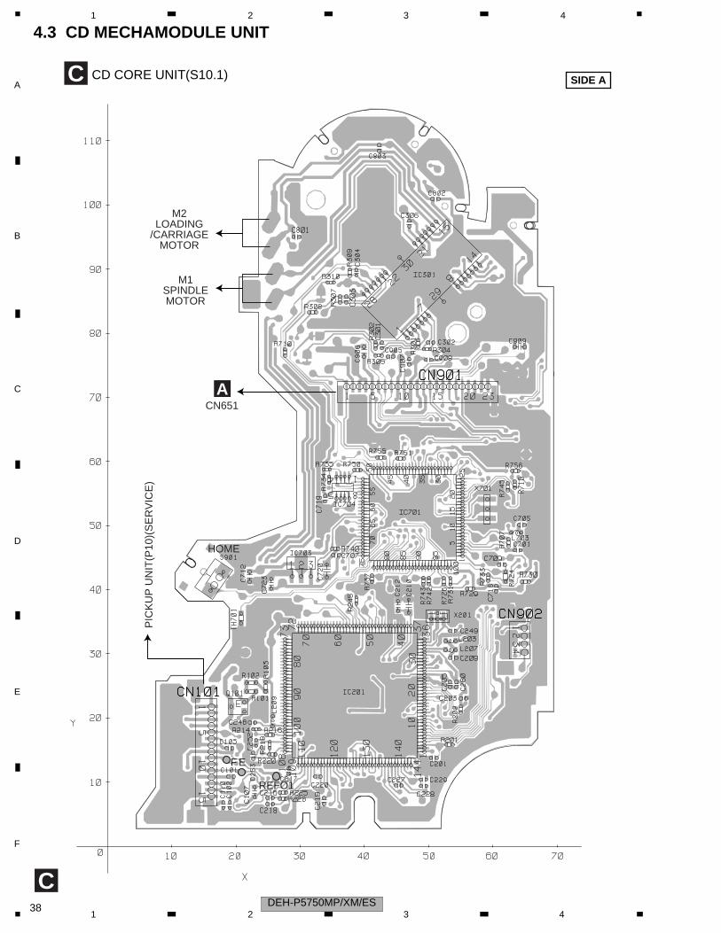
4.3 CD MECHAMODULE UNIT
C
C CD CORE UNIT(S10.1) SIDE A
ACN651
PIC
KU
P U
NIT
(P10
)(S
ER
VIC
E)
HOME
M2LOADING
/CARRIAGEMOTOR
M1SPINDLEMOTOR
EF
REFO1
DEH-P5750MP/XM/ES381 2 3 4
C
D
F
A
B
E
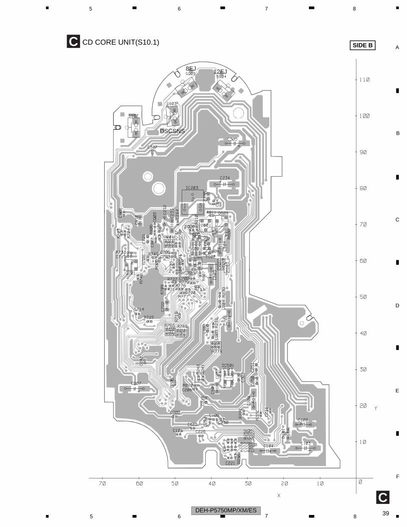
5 6 7 8
C
C CD CORE UNIT(S10.1) SIDE B
12EJ8EJ
DSCSNS
DEH-P5750MP/XM/ES 395 6 7 8
C
D
F
A
B
E
1 2 3 4
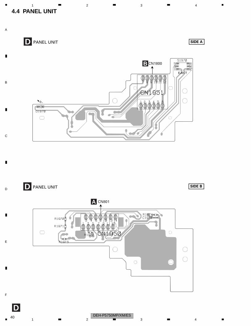
4.4 PANEL UNIT
D
D PANEL UNIT
D PANEL UNIT
SIDE A
SIDE B
B CN1800
A CN801
EJECT
DEH-P5750MP/XM/ES401 2 3 4
C
D
F
A
B
E
5 6 7 8
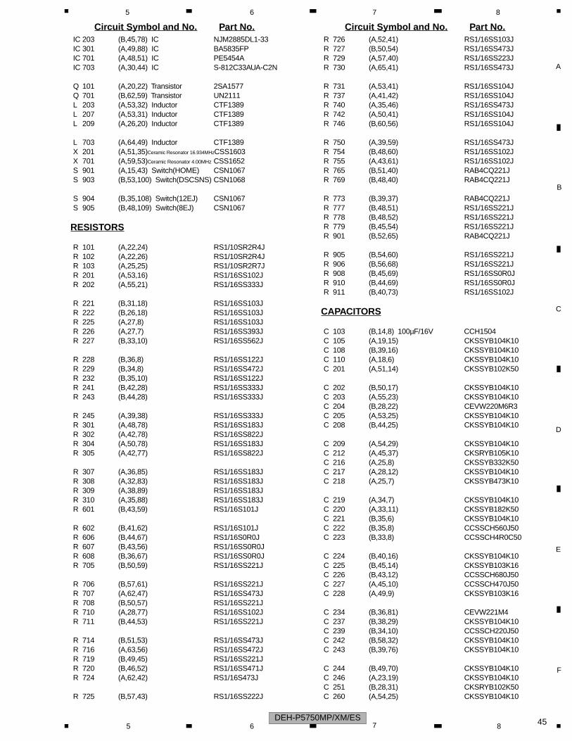
5. ELECTRICAL PARTS LIST
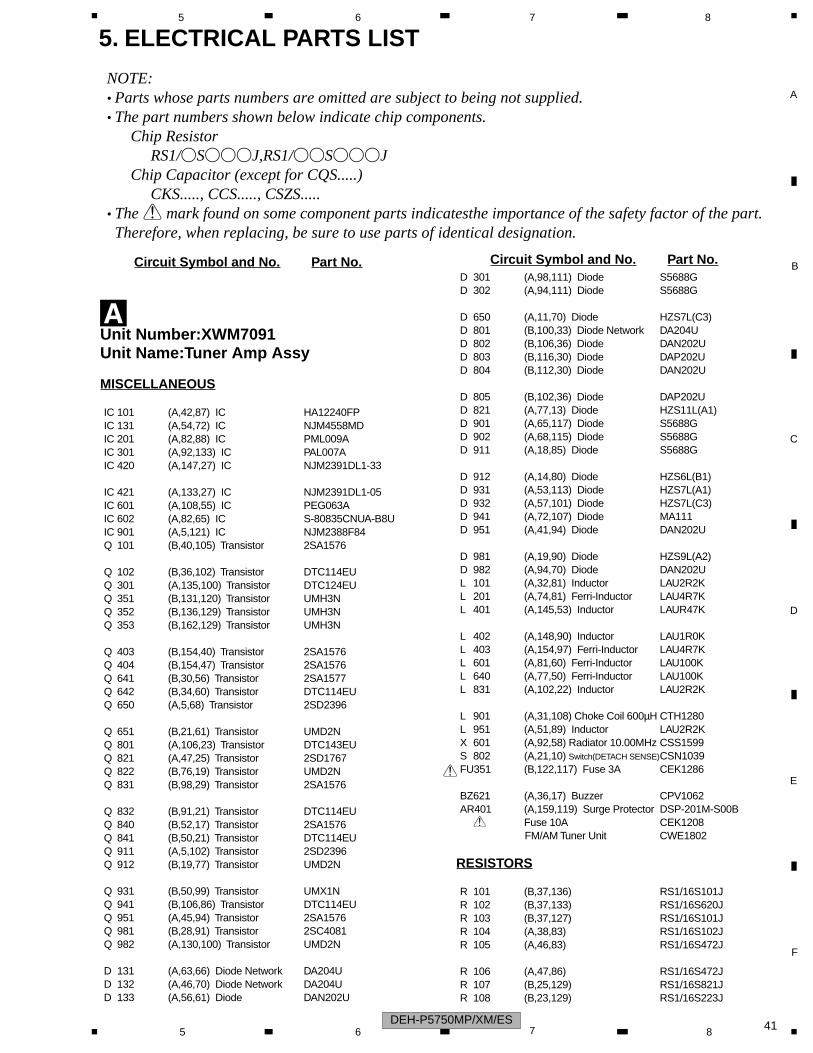
NOTE:• Parts whose parts numbers are omitted are subject to being not supplied.• The part numbers shown below indicate chip components. Chip Resistor RS1/_S___J,RS1/__S___J Chip Capacitor (except for CQS.....) CKS....., CCS....., CSZS.....• The > mark found on some component parts indicatesthe importance of the safety factor of the part. Therefore, when replacing, be sure to use parts of identical designation.
Circuit Symbol and No. Part No.
AUnit Number:XWM7091Unit Name:Tuner Amp Assy
MISCELLANEOUS
IC 101 (A,42,87) IC HA12240FPIC 131 (A,54,72) IC NJM4558MDIC 201 (A,82,88) IC PML009AIC 301 (A,92,133) IC PAL007AIC 420 (A,147,27) IC NJM2391DL1-33
IC 421 (A,133,27) IC NJM2391DL1-05IC 601 (A,108,55) IC PEG063AIC 602 (A,82,65) IC S-80835CNUA-B8UIC 901 (A,5,121) IC NJM2388F84Q 101 (B,40,105) Transistor 2SA1576
Q 102 (B,36,102) Transistor DTC114EUQ 301 (A,135,100) Transistor DTC124EUQ 351 (B,131,120) Transistor UMH3NQ 352 (B,136,129) Transistor UMH3NQ 353 (B,162,129) Transistor UMH3N
Q 403 (B,154,40) Transistor 2SA1576Q 404 (B,154,47) Transistor 2SA1576Q 641 (B,30,56) Transistor 2SA1577Q 642 (B,34,60) Transistor DTC114EUQ 650 (A,5,68) Transistor 2SD2396
Q 651 (B,21,61) Transistor UMD2NQ 801 (A,106,23) Transistor DTC143EUQ 821 (A,47,25) Transistor 2SD1767Q 822 (B,76,19) Transistor UMD2NQ 831 (B,98,29) Transistor 2SA1576
Q 832 (B,91,21) Transistor DTC114EUQ 840 (B,52,17) Transistor 2SA1576Q 841 (B,50,21) Transistor DTC114EUQ 911 (A,5,102) Transistor 2SD2396Q 912 (B,19,77) Transistor UMD2N
Q 931 (B,50,99) Transistor UMX1NQ 941 (B,106,86) Transistor DTC114EUQ 951 (A,45,94) Transistor 2SA1576Q 981 (B,28,91) Transistor 2SC4081Q 982 (A,130,100) Transistor UMD2N
D 131 (A,63,66) Diode Network DA204UD 132 (A,46,70) Diode Network DA204UD 133 (A,56,61) Diode DAN202U
D 301 (A,98,111) Diode S5688GD 302 (A,94,111) Diode S5688G
D 650 (A,11,70) Diode HZS7L(C3)D 801 (B,100,33) Diode Network DA204UD 802 (B,106,36) Diode DAN202UD 803 (B,116,30) Diode DAP202UD 804 (B,112,30) Diode DAN202U
D 805 (B,102,36) Diode DAP202UD 821 (A,77,13) Diode HZS11L(A1)D 901 (A,65,117) Diode S5688GD 902 (A,68,115) Diode S5688GD 911 (A,18,85) Diode S5688G
D 912 (A,14,80) Diode HZS6L(B1)D 931 (A,53,113) Diode HZS7L(A1)D 932 (A,57,101) Diode HZS7L(C3)D 941 (A,72,107) Diode MA111D 951 (A,41,94) Diode DAN202U
D 981 (A,19,90) Diode HZS9L(A2)D 982 (A,94,70) Diode DAN202UL 101 (A,32,81) Inductor LAU2R2KL 201 (A,74,81) Ferri-Inductor LAU4R7KL 401 (A,145,53) Inductor LAUR47K
L 402 (A,148,90) Inductor LAU1R0KL 403 (A,154,97) Ferri-Inductor LAU4R7KL 601 (A,81,60) Ferri-Inductor LAU100KL 640 (A,77,50) Ferri-Inductor LAU100KL 831 (A,102,22) Inductor LAU2R2K
L 901 (A,31,108) Choke Coil 600µH CTH1280L 951 (A,51,89) Inductor LAU2R2KX 601 (A,92,58) Radiator 10.00MHz CSS1599S 802 (A,21,10) Switch(DETACH SENSE)CSN1039FU351 (B,122,117) Fuse 3A CEK1286
BZ621 (A,36,17) Buzzer CPV1062AR401 (A,159,119) Surge Protector DSP-201M-S00B
> Fuse 10A CEK1208FM/AM Tuner Unit CWE1802
RESISTORS
R 101 (B,37,136) RS1/16S101JR 102 (B,37,133) RS1/16S620JR 103 (B,37,127) RS1/16S101JR 104 (A,38,83) RS1/16S102JR 105 (A,46,83) RS1/16S472J
R 106 (A,47,86) RS1/16S472JR 107 (B,25,129) RS1/16S821JR 108 (B,23,129) RS1/16S223J
Circuit Symbol and No. Part No.
>
DEH-P5750MP/XM/ES 415 6 7 8
C
D
F
A
B
E
1 2 3 4
R 109 (B,33,105) RS1/16S222JR 110 (B,30,121) RS1/16S821J
R 111 (B,29,121) RS1/16S223JR 112 (B,27,121) RS1/16S102JR 113 (B,24,134) RS1/16S102JR 114 (B,42,107) RS1/16S223JR 115 (B,37,107) RS1/16S472J
R 131 (A,60,69) RS1/16S563JR 132 (A,49,71) RS1/16S563JR 133 (A,60,72) RS1/16S104JR 134 (A,49,74) RS1/16S104JR 135 (A,61,62) RS1/16S474J
R 136 (A,54,65) RS1/16S474JR 201 (A,111,73) RAB4C102JR 220 (A,76,95) RS1/16S102JR 221 (B,74,86) RS1/16S102JR 222 (B,90,96) RS1/16S471J
R 223 (B,85,82) RS1/16S471JR 224 (B,92,94) RS1/16S471JR 225 (B,93,84) RS1/16S471JR 301 (A,138,97) RS1/16S103JR 302 (A,135,96) RS1/16S331J
R 303 (A,135,98) RS1/16S103JR 304 (B,118,128) RS1/16S153JR 351 (B,144,108) RS1/16S471JR 352 (B,144,118) RS1/16S471JR 353 (B,139,121) RS1/16S471J
R 354 (B,138,119) RS1/16S471JR 355 (B,158,124) RS1/16S821JR 356 (B,141,128) RS1/16S821JR 357 (B,132,117) RS1/16S223JR 358 (B,131,122) RS1/16S223J
R 359 (B,139,129) RS1/16S223JR 360 (B,127,135) RS1/16S223JR 361 (B,159,133) RS1/16S223JR 362 (B,157,128) RS1/16S223JR 401 (B,145,62) RS1/16S0R0J
R 403 (B,158,71) RS1/16S681JR 404 (A,99,72) RS1/16S681JR 406 (B,155,80) RS1/16S681JR 407 (B,113,50) RS1/16S681JR 408 (B,155,82) RS1/16S681J
R 409 (B,155,84) RS1/16S681JR 410 (B,119,54) RS1/16S681JR 411 (B,155,86) RS1/16S681JR 412 (B,119,56) RS1/16S681JR 413 (B,157,90) RS1/16S681J
R 416 (B,149,40) RS1/16S222JR 417 (B,149,42) RS1/16S561JR 418 (B,150,46) RS1/16S561JR 419 (B,152,50) RS1/16S222JR 421 (B,145,51) RS1/16S471J
R 424 (A,98,67) RS1/16S471JR 603 (B,110,64) RS1/16S104JR 605 (B,107,61) RS1/16S104JR 606 (A,91,65) RS1/16S104JR 607 (B,64,58) RS1/16S822J
R 608 (A,74,66) RS1/16S102JR 609 (A,95,45) RS1/16S102JR 610 (A,80,51) RS1/16S104J
Circuit Symbol and No. Part No.R 611 (A,93,48) RS1/16S473JR 613 (B,85,34) RS1/16S221J
R 614 (B,83,29) RS1/16S682JR 615 (A,65,30) RS1/16S682JR 616 (A,65,25) RS1/16S221JR 621 (B,42,19) RS1/16S102JR 631 (A,122,60) RS1/16S104J
R 641 (B,33,51) RS1/16S103JR 643 (B,36,55) RS1/16S182JR 646 (B,81,41) RS1/16S102JR 647 (A,74,52) RS1/16S102JR 648 (B,52,31) RS1/16S222J
R 649 (B,83,39) RS1/16S104JR 650 (A,11,64) RD1/4PU0R0JR 651 (A,16,61) RD1/4PU271JR 652 (A,16,67) RD1/4PU221JR 666 (B,55,44) RS1/16S104J
R 667 (B,61,42) RS1/16S102JR 668 (B,59,36) RS1/16S102JR 801 (B,122,28) RS1/16S102JR 802 (B,26,20) RS1/16S104JR 803 (B,26,16) RS1/16S102J
R 804 (B,122,24) RS1/16S222JR 805 (B,118,39) RS1/16S222JR 806 (B,120,24) RS1/16S222JR 807 (B,117,25) RS1/16S222JR 808 (B,111,23) RS1/16S222J
R 809 (B,104,25) RS1/16S222JR 810 (B,115,43) RS1/16S102JR 811 (B,121,30) RS1/16S102JR 812 (B,111,34) RS1/16S102JR 813 (A,77,16) RS1/16S1R0J
R 814 (B,107,24) RS1/16S222JR 815 (A,102,38) RS1/16S473JR 816 (B,111,26) RS1/16S473JR 817 (B,105,31) RS1/16S473JR 818 (B,115,45) RS1/16S104J
R 821 (A,61,13) RD1/4PU391JR 822 (B,61,16) RS1/16S391JR 823 (B,66,16) RS1/16S391JR 824 (A,75,17) RS1/16S472JR 831 (B,94,29) RS1/16S473J
R 832 (B,92,29) RS1/16S102JR 833 (B,99,23) RS1/16S222JR 840 (B,48,18) RS1/16S103JR 841 (B,46,20) RS1/16S103JR 901 (B,16,99) RS1/16S102J
R 902 (B,18,102) RS1/16S103JR 911 (B,9,107) RS1/16S391JR 912 (B,11,81) RS1/16S222JR 913 (B,11,86) RS1/16S223JR 914 (B,48,94) RS1/16S104J
R 915 (B,46,98) RS1/16S104JR 916 (A,106,73) RS1/16S104JR 931 (A,49,108) RD1/4PU102JR 932 (B,46,105) RS1/16S472JR 933 (B,52,102) RS1/16S473J
R 934 (B,54,102) RS1/16S103JR 935 (B,48,105) RS1/16S473JR 936 (B,44,99) RS1/16S104J
Circuit Symbol and No. Part No.
DEH-P5750MP/XM/ES421 2 3 4
C
D
F
A
B
E
5 6 7 8
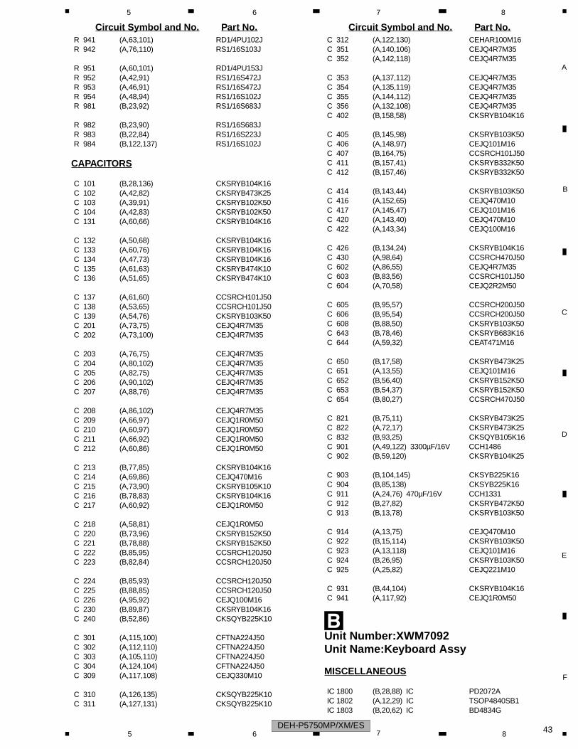
R 941 (A,63,101) RD1/4PU102JR 942 (A,76,110) RS1/16S103J
R 951 (A,60,101) RD1/4PU153JR 952 (A,42,91) RS1/16S472JR 953 (A,46,91) RS1/16S472JR 954 (A,48,94) RS1/16S102JR 981 (B,23,92) RS1/16S683J
R 982 (B,23,90) RS1/16S683JR 983 (B,22,84) RS1/16S223JR 984 (B,122,137) RS1/16S102J
CAPACITORS
C 101 (B,28,136) CKSRYB104K16C 102 (A,42,82) CKSRYB473K25C 103 (A,39,91) CKSRYB102K50C 104 (A,42,83) CKSRYB102K50C 131 (A,60,66) CKSRYB104K16
C 132 (A,50,68) CKSRYB104K16C 133 (A,60,76) CKSRYB104K16C 134 (A,47,73) CKSRYB104K16C 135 (A,61,63) CKSRYB474K10C 136 (A,51,65) CKSRYB474K10
C 137 (A,61,60) CCSRCH101J50C 138 (A,53,65) CCSRCH101J50C 139 (A,54,76) CKSRYB103K50C 201 (A,73,75) CEJQ4R7M35C 202 (A,73,100) CEJQ4R7M35
C 203 (A,76,75) CEJQ4R7M35C 204 (A,80,102) CEJQ4R7M35C 205 (A,82,75) CEJQ4R7M35C 206 (A,90,102) CEJQ4R7M35C 207 (A,88,76) CEJQ4R7M35
C 208 (A,86,102) CEJQ4R7M35C 209 (A,66,97) CEJQ1R0M50C 210 (A,60,97) CEJQ1R0M50C 211 (A,66,92) CEJQ1R0M50C 212 (A,60,86) CEJQ1R0M50
C 213 (B,77,85) CKSRYB104K16C 214 (A,69,86) CEJQ470M16C 215 (A,73,90) CKSRYB105K10C 216 (B,78,83) CKSRYB104K16C 217 (A,60,92) CEJQ1R0M50
C 218 (A,58,81) CEJQ1R0M50C 220 (B,73,96) CKSRYB152K50C 221 (B,78,88) CKSRYB152K50C 222 (B,85,95) CCSRCH120J50C 223 (B,82,84) CCSRCH120J50
C 224 (B,85,93) CCSRCH120J50C 225 (B,88,85) CCSRCH120J50C 226 (A,95,92) CEJQ100M16C 230 (B,89,87) CKSRYB104K16C 240 (B,52,86) CKSQYB225K10
C 301 (A,115,100) CFTNA224J50C 302 (A,112,110) CFTNA224J50C 303 (A,105,110) CFTNA224J50C 304 (A,124,104) CFTNA224J50C 309 (A,117,108) CEJQ330M10
C 310 (A,126,135) CKSQYB225K10C 311 (A,127,131) CKSQYB225K10
Circuit Symbol and No. Part No.C 312 (A,122,130) CEHAR100M16C 351 (A,140,106) CEJQ4R7M35C 352 (A,142,118) CEJQ4R7M35
C 353 (A,137,112) CEJQ4R7M35C 354 (A,135,119) CEJQ4R7M35C 355 (A,144,112) CEJQ4R7M35C 356 (A,132,108) CEJQ4R7M35C 402 (B,158,58) CKSRYB104K16
C 405 (B,145,98) CKSRYB103K50C 406 (A,148,97) CEJQ101M16C 407 (B,164,75) CCSRCH101J50C 411 (B,157,41) CKSRYB332K50C 412 (B,157,46) CKSRYB332K50
C 414 (B,143,44) CKSRYB103K50C 416 (A,152,65) CEJQ470M10C 417 (A,145,47) CEJQ101M16C 420 (A,143,40) CEJQ470M10C 422 (A,143,34) CEJQ100M16
C 426 (B,134,24) CKSRYB104K16C 430 (A,98,64) CCSRCH470J50C 602 (A,86,55) CEJQ4R7M35C 603 (B,83,56) CCSRCH101J50C 604 (A,70,58) CEJQ2R2M50
C 605 (B,95,57) CCSRCH200J50C 606 (B,95,54) CCSRCH200J50C 608 (B,88,50) CKSRYB103K50C 643 (B,78,46) CKSRYB683K16C 644 (A,59,32) CEAT471M16
C 650 (B,17,58) CKSRYB473K25C 651 (A,13,55) CEJQ101M16C 652 (B,56,40) CKSRYB152K50C 653 (B,54,37) CKSRYB152K50C 654 (B,80,27) CCSRCH470J50
C 821 (B,75,11) CKSRYB473K25C 822 (A,72,17) CKSRYB473K25C 832 (B,93,25) CKSQYB105K16C 901 (A,49,122) 3300µF/16V CCH1486C 902 (B,59,120) CKSRYB104K25
C 903 (B,104,145) CKSYB225K16C 904 (B,85,138) CKSYB225K16C 911 (A,24,76) 470µF/16V CCH1331C 912 (B,27,82) CKSRYB472K50C 913 (B,13,78) CKSRYB103K50
C 914 (A,13,75) CEJQ470M10C 922 (B,15,114) CKSRYB103K50C 923 (A,13,118) CEJQ101M16C 924 (B,26,95) CKSRYB103K50C 925 (A,25,82) CEJQ221M10
C 931 (B,44,104) CKSRYB104K16C 941 (A,117,92) CEJQ1R0M50
BUnit Number:XWM7092Unit Name:Keyboard Assy
MISCELLANEOUS
IC 1800 (B,28,88) IC PD2072AIC 1802 (A,12,29) IC TSOP4840SB1IC 1803 (B,20,62) IC BD4834G
Circuit Symbol and No. Part No.
DEH-P5750MP/XM/ES 435 6 7 8
C
D
F
A
B
E
1 2 3 4
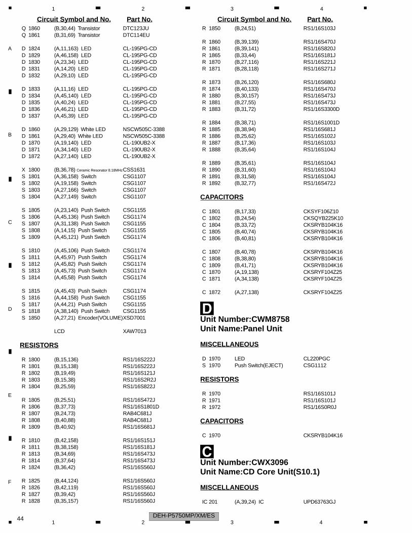
Q 1860 (B,30,44) Transistor DTC123JUQ 1861 (B,31,69) Transistor DTC114EU
D 1824 (A,11,163) LED CL-195PG-CDD 1829 (A,46,158) LED CL-195PG-CDD 1830 (A,23,34) LED CL-195PG-CDD 1831 (A,14,20) LED CL-195PG-CDD 1832 (A,29,10) LED CL-195PG-CD
D 1833 (A,11,16) LED CL-195PG-CDD 1834 (A,45,140) LED CL-195PG-CDD 1835 (A,40,24) LED CL-195PG-CDD 1836 (A,46,21) LED CL-195PG-CDD 1837 (A,45,39) LED CL-195PG-CD
D 1860 (A,29,129) White LED NSCW505C-3388D 1861 (A,29,40) White LED NSCW505C-3388D 1870 (A,19,140) LED CL-190UB2-XD 1871 (A,34,140) LED CL-190UB2-XD 1872 (A,27,140) LED CL-190UB2-X
X 1800 (B,36,78) Ceramic Resonator 8.18MHzCSS1631S 1801 (A,36,158) Switch CSG1107S 1802 (A,19,158) Switch CSG1107S 1803 (A,27,166) Switch CSG1107S 1804 (A,27,149) Switch CSG1107
S 1805 (A,23,140) Push Switch CSG1155S 1806 (A,45,136) Push Switch CSG1174S 1807 (A,31,138) Push Switch CSG1155S 1808 (A,14,15) Push Switch CSG1155S 1809 (A,45,121) Push Switch CSG1174
S 1810 (A,45,106) Push Switch CSG1174S 1811 (A,45,97) Push Switch CSG1174S 1812 (A,45,82) Push Switch CSG1174S 1813 (A,45,73) Push Switch CSG1174S 1814 (A,45,58) Push Switch CSG1174
S 1815 (A,45,43) Push Switch CSG1174S 1816 (A,44,158) Push Switch CSG1155S 1817 (A,44,21) Push Switch CSG1155S 1818 (A,38,140) Push Switch CSG1155S 1850 (A,27,21) Encoder(VOLUME)XSD7001
LCD XAW7013
RESISTORS
R 1800 (B,15,136) RS1/16S222JR 1801 (B,15,138) RS1/16S222JR 1802 (B,19,49) RS1/16S121JR 1803 (B,15,38) RS1/16S2R2JR 1804 (B,25,59) RS1/16S822J
R 1805 (B,25,51) RS1/16S472JR 1806 (B,37,73) RS1/16S1801DR 1807 (B,24,73) RAB4C681JR 1808 (B,40,88) RAB4C681JR 1809 (B,40,92) RS1/16S681J
R 1810 (B,42,158) RS1/16S151JR 1811 (B,38,158) RS1/16S181JR 1813 (B,34,69) RS1/16S473JR 1814 (B,37,64) RS1/16S473JR 1824 (B,36,42) RS1/16S560J
R 1825 (B,44,124) RS1/16S560JR 1826 (B,42,119) RS1/16S560JR 1827 (B,39,42) RS1/16S560JR 1828 (B,35,157) RS1/16S560J
Circuit Symbol and No. Part No.R 1850 (B,24,51) RS1/16S103J
R 1860 (B,39,139) RS1/16S470JR 1861 (B,39,141) RS1/16S820JR 1865 (B,33,44) RS1/16S181JR 1870 (B,27,116) RS1/16S221JR 1871 (B,28,118) RS1/16S271J
R 1873 (B,26,120) RS1/16S680JR 1874 (B,40,133) RS1/16S470JR 1880 (B,30,157) RS1/16S473JR 1881 (B,27,55) RS1/16S473JR 1883 (B,31,72) RS1/16S3300D
R 1884 (B,38,71) RS1/16S1001DR 1885 (B,38,94) RS1/16S681JR 1886 (B,25,62) RS1/16S102JR 1887 (B,17,36) RS1/16S103JR 1888 (B,35,64) RS1/16S104J
R 1889 (B,35,61) RS1/16S104JR 1890 (B,31,60) RS1/16S104JR 1891 (B,31,58) RS1/16S104JR 1892 (B,32,77) RS1/16S472J
CAPACITORS
C 1801 (B,17,33) CKSYF106Z10C 1802 (B,24,54) CKSQYB225K10C 1804 (B,33,72) CKSRYB104K16C 1805 (B,40,74) CKSRYB104K16C 1806 (B,40,81) CKSRYB104K16
C 1807 (B,40,78) CKSRYB104K16C 1808 (B,38,80) CKSRYB104K16C 1809 (B,41,71) CKSRYB104K16C 1870 (A,19,138) CKSRYF104Z25C 1871 (A,34,138) CKSRYF104Z25
C 1872 (A,27,138) CKSRYF104Z25
DUnit Number:CWM8758Unit Name:Panel Unit
MISCELLANEOUS
D 1970 LED CL220PGCS 1970 Push Switch(EJECT) CSG1112
RESISTORS
R 1970 RS1/16S101JR 1971 RS1/16S101JR 1972 RS1/16S0R0J
CAPACITORS
C 1970 CKSRYB104K16
CUnit Number:CWX3096Unit Name:CD Core Unit(S10.1)
MISCELLANEOUS
IC 201 (A,39,24) IC UPD63763GJ
Circuit Symbol and No. Part No.
DEH-P5750MP/XM/ES441 2 3 4
C
D
F
A
B
E
5 6 7 8
IC 203 (B,45,78) IC NJM2885DL1-33IC 301 (A,49,88) IC BA5835FPIC 701 (A,48,51) IC PE5454AIC 703 (A,30,44) IC S-812C33AUA-C2N
Q 101 (A,20,22) Transistor 2SA1577Q 701 (B,62,59) Transistor UN2111L 203 (A,53,32) Inductor CTF1389L 207 (A,53,31) Inductor CTF1389L 209 (A,26,20) Inductor CTF1389
L 703 (A,64,49) Inductor CTF1389X 201 (A,51,35)Ceramic Resonator 16.934MHzCSS1603X 701 (A,59,53)Ceramic Resonator 4.00MHz CSS1652S 901 (A,15,43) Switch(HOME) CSN1067S 903 (B,53,100) Switch(DSCSNS) CSN1068
S 904 (B,35,108) Switch(12EJ) CSN1067S 905 (B,48,109) Switch(8EJ) CSN1067
RESISTORS
R 101 (A,22,24) RS1/10SR2R4JR 102 (A,22,26) RS1/10SR2R4JR 103 (A,25,25) RS1/10SR2R7JR 201 (A,53,16) RS1/16SS102JR 202 (A,55,21) RS1/16SS333J
R 221 (B,31,18) RS1/16SS103JR 222 (B,26,18) RS1/16SS103JR 225 (A,27,8) RS1/16SS103JR 226 (A,27,7) RS1/16SS393JR 227 (B,33,10) RS1/16SS562J
R 228 (B,36,8) RS1/16SS122JR 229 (B,34,8) RS1/16SS472JR 232 (B,35,10) RS1/16SS122JR 241 (B,42,28) RS1/16SS333JR 243 (B,44,28) RS1/16SS333J
R 245 (A,39,38) RS1/16SS333JR 301 (A,48,78) RS1/16SS183JR 302 (A,42,78) RS1/16SS822JR 304 (A,50,78) RS1/16SS183JR 305 (A,42,77) RS1/16SS822J
R 307 (A,36,85) RS1/16SS183JR 308 (A,32,83) RS1/16SS183JR 309 (A,38,89) RS1/16SS183JR 310 (A,35,88) RS1/16SS183JR 601 (B,43,59) RS1/16S101J
R 602 (B,41,62) RS1/16S101JR 606 (B,44,67) RS1/16S0R0JR 607 (B,43,56) RS1/16SS0R0JR 608 (B,36,67) RS1/16SS0R0JR 705 (B,50,59) RS1/16SS221J
R 706 (B,57,61) RS1/16SS221JR 707 (A,62,47) RS1/16SS473JR 708 (B,50,57) RS1/16SS221JR 710 (A,28,77) RS1/16SS102JR 711 (B,44,53) RS1/16SS221J
R 714 (B,51,53) RS1/16SS473JR 716 (A,63,56) RS1/16SS472JR 719 (B,49,45) RS1/16SS221JR 720 (B,46,52) RS1/16SS471JR 724 (A,62,42) RS1/16S473J
R 725 (B,57,43) RS1/16SS222J
Circuit Symbol and No. Part No.R 726 (A,52,41) RS1/16SS103JR 727 (B,50,54) RS1/16SS473JR 729 (A,57,40) RS1/16SS223JR 730 (A,65,41) RS1/16SS473J
R 731 (A,53,41) RS1/16SS104JR 737 (A,41,42) RS1/16SS104JR 740 (A,35,46) RS1/16SS473JR 742 (A,50,41) RS1/16SS104JR 746 (B,60,56) RS1/16SS104J
R 750 (A,39,59) RS1/16SS473JR 754 (B,48,60) RS1/16SS102JR 755 (A,43,61) RS1/16SS102JR 765 (B,51,40) RAB4CQ221JR 769 (B,48,40) RAB4CQ221J
R 773 (B,39,37) RAB4CQ221JR 777 (B,48,51) RS1/16SS221JR 778 (B,48,52) RS1/16SS221JR 779 (B,45,54) RS1/16SS221JR 901 (B,52,65) RAB4CQ221J
R 905 (B,54,60) RS1/16SS221JR 906 (B,56,68) RS1/16SS221JR 908 (B,45,69) RS1/16SS0R0JR 910 (B,44,69) RS1/16SS0R0JR 911 (B,40,73) RS1/16SS102J
CAPACITORS
C 103 (B,14,8) 100µF/16V CCH1504C 105 (A,19,15) CKSSYB104K10C 108 (B,39,16) CKSSYB104K10C 110 (A,18,6) CKSSYB104K10C 201 (A,51,14) CKSSYB102K50
C 202 (B,50,17) CKSSYB104K10C 203 (A,55,23) CKSSYB104K10C 204 (B,28,22) CEVW220M6R3C 205 (A,53,25) CKSSYB104K10C 208 (B,44,25) CKSSYB104K10
C 209 (A,54,29) CKSSYB104K10C 212 (A,45,37) CKSRYB105K10C 216 (A,25,8) CKSSYB332K50C 217 (A,28,12) CKSSYB104K10C 218 (A,25,7) CKSSYB473K10
C 219 (A,34,7) CKSSYB104K10C 220 (A,33,11) CKSSYB182K50C 221 (B,35,6) CKSSYB104K10C 222 (B,35,8) CCSSCH560J50C 223 (B,33,8) CCSSCH4R0C50
C 224 (B,40,16) CKSSYB104K10C 225 (B,45,14) CKSSYB103K16C 226 (B,43,12) CCSSCH680J50C 227 (A,45,10) CCSSCH470J50C 228 (A,49,9) CKSSYB103K16
C 234 (B,36,81) CEVW221M4C 237 (B,38,29) CKSSYB104K10C 239 (B,34,10) CCSSCH220J50C 242 (B,58,32) CKSSYB104K10C 243 (B,39,76) CKSSYB104K10
C 244 (B,49,70) CKSSYB104K10C 246 (A,23,19) CKSSYB104K10C 251 (B,28,31) CKSRYB102K50C 260 (A,54,25) CKSSYB104K10
Circuit Symbol and No. Part No.
DEH-P5750MP/XM/ES 455 6 7 8
C
D
F
A
B
E
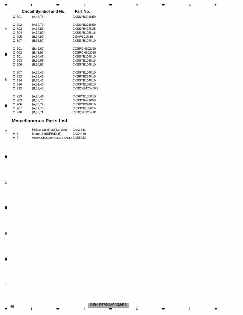
1 2 3 4
C 301 (A,43,78) CKSSYB221K50
C 302 (A,50,79) CKSSYB221K50C 303 (A,37,85) CKSSYB472K25C 304 (A,39,89) CKSSYB103K16C 305 (B,34,92) CEVW101M16C 307 (B,56,90) CKSSYB104K10
C 601 (B,46,60) CCSRCH102J50C 602 (B,41,65) CCSRCH102J50C 701 (A,64,46) CKSSYB104K10C 703 (B,50,61) CKSSYB103K16C 706 (B,50,62) CKSSYB104K10
C 707 (A,36,45) CKSSYB104K10C 712 (A,22,42) CKSRYB224K16C 714 (B,60,45) CKSSYB104K10C 716 (A,61,40) CKSSYB103K16C 722 (B,52,48) CKSQYB475K6R3
C 723 (A,26,41) CKSRYB105K10C 903 (B,56,70) CKSSYB471K50C 906 (A,40,77) CKSRYB224K16C 907 (A,47,76) CKSSYB103K16C 910 (B,60,71) CKSQYB225K10
Miscellaneous Parts List
Pickup Unit(P10)(Service) CXX1641M 1 Motor Unit(SPINDLE) CXC4440M 2 Motor Unit(LOADING/CARRIAGE) CXB8933
Circuit Symbol and No. Part No.
DEH-P5750MP/XM/ES461 2 3 4
C
D
F
A
B
E
5 6 7 8
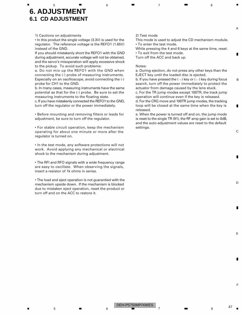
6. ADJUSTMENT6.1 CD ADJUSTMENT
1) Cautions on adjustments• In this product the single voltage (3.3V) is used for the regulator. The reference voltage is the REFO1 (1.65V) instead of the GND.If you should mistakenly short the REFO1 with the GND during adjustment, accurate voltage will not be obtained, and the servo’s misoperation will apply excessive shock to the pickup. To avoid such problems:a. Do not mix up the REFO1 with the GND when connecting the (-) probe of measuring instruments. Especially on an oscilloscope, avoid connecting the (-) probe for CH1 to the GND. b. In many cases, measuring instruments have the same potential as that for the (-) probe. Be sure to set the measuring instruments to the floating state.c. If you have mistakenly connected the REFO1 to the GND, turn off the regulator or the power immediately.
• Before mounting and removing filters or leads for adjustment, be sure to turn off the regulator.
• For stable circuit operation, keep the mechanism operating for about one minute or more after the regulator is turned on.
• In the test mode, any software protections will not work. Avoid applying any mechanical or electrical shock to the mechanism during adjustment.
• The RFI and RFO signals with a wide frequency range are easy to oscillate. When observing the signals, insert a resistor of 1k ohms in series.
• The load and eject operation is not guarantied with the mechanism upside down. If the mechanism is blocked due to mistaken eject operation, reset the product or turn off and on the ACC to restore it.
2) Test modeThis mode is used to adjust the CD mechanism module.• To enter the test mode.While pressing the 4 and 6 keys at the same time, reset.• To exit from the test mode.Turn off the ACC and back up.
Notes:a. During ejection, do not press any other keys than the EJECT key until the loaded disc is ejected.b. If you have pressed the (→) key or (←) key during focus search, turn off the power immediately to protect the actuator from damage caused by the lens stuck.c. For the TR jump modes except 100TR, the track jump operation will continue even if the key is released.d. For the CRG move and 100TR jump modes, the tracking loop will be closed at the same time when the key is released.e. When the power is turned off and on, the jump mode is reset to the single TR (91), the RF amp gain is set to 0dB, and the auto-adjustment values are reset to the default settings.
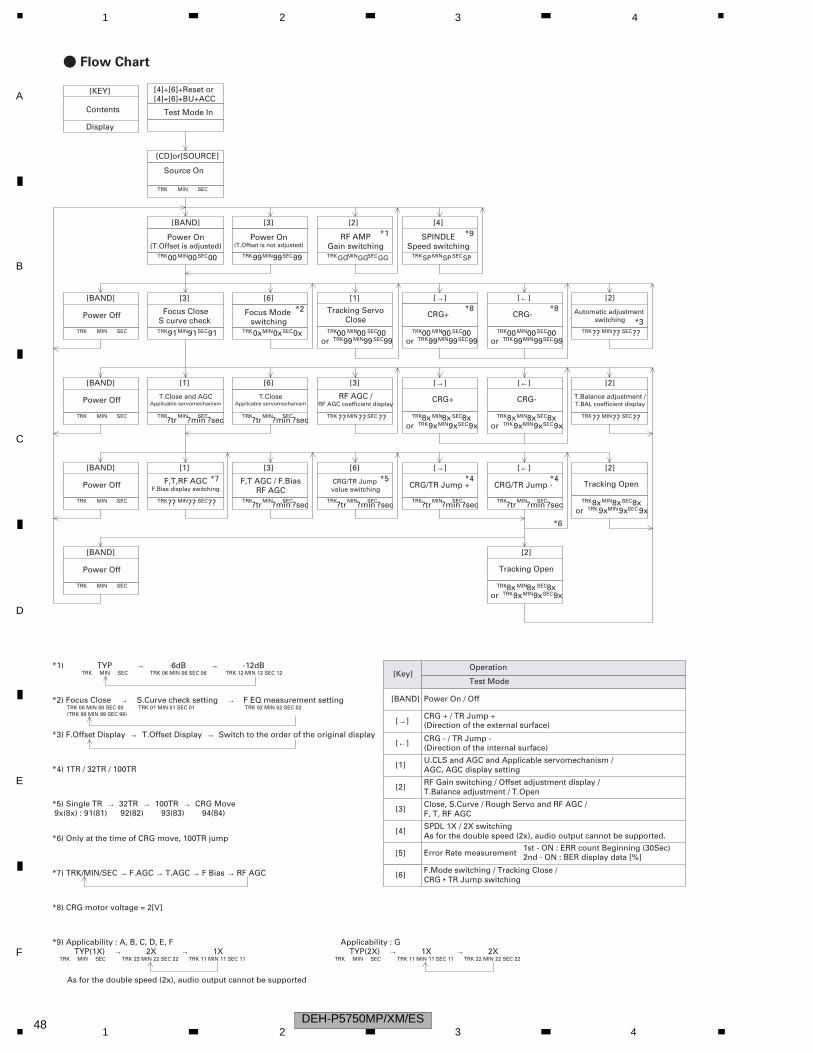
DEH-P5750MP/XM/ES 475 6 7 8
C
D
F
A
B
E
1 2 3 4
[BAND]
[BAND]
[BAND]
[BAND]
[BAND]
Power On(T.Offset is adjusted)
TRK00 MIN00 SEC
SEC
00
[CD]or[SOURCE]
Source On
TRK MIN
[4]+[6]+Reset or [4]+[6]+BU+ACC
Test Mode In
[3]
[1]
[1]
Power On(T.Offset is not adjusted)
TRK99 MIN99 SEC99
[2]
[2]
[2]
[2]
Power Off
TRK MIN SEC
Power Off
TRK MIN SEC
Power Off
TRK MIN SEC
Power Off
TRK MIN SEC
Focus CloseS curve check
T.Close and AGCApplicable servomechanism
TRK91 MIN91 SEC91
[6] [1]
[3]
[6]
[3]
Focus Mode switching
SPINDLESpeed switching
RF AMPGain switching
TRK0xMIN0xSEC0x
Tracking ServoClose
TRK00 MIN00 SEC00or TRK99 MIN99 SEC99
CRG-
TRK00 MIN00 SEC00or TRK99 MIN99 SEC99
[→] [←]
[→] [←]
[→] [←]
CRG+
TRK00 MIN00 SEC00or TRK99 MIN99 SEC99
Automatic adjustment switching
TRK?? MIN?? SEC??
T.CloseApplicable servomechanism
TRK?tr
MIN?min
SEC?sec
[6]
[3]
TRK MIN SEC
RF AGC /RF AGC coefficient display
TRK?? MIN?? SEC??
CRG+
TRK8x MIN8x SEC8xor TRK9xMIN9xSEC9x
CRG-
TRK8xMIN8xSEC8xor TRK9xMIN9xSEC9x
T.Balance adjustment /T.BAL coefficient display
TRK?? MIN?? SEC??
F,T,RF AGCF.Bias display switching
TRK?? MIN?? SEC??
F,T AGC / F.BiasRF AGC
TRK MIN SEC
CRG/TR Jump value switching
TRK MIN SEC
CRG/TR Jump +
TRK MIN SEC
CRG/TR Jump -
TRK MIN SEC
Tracking Open
TRK8xMIN8xSEC8xor TRK 9xMIN9xSEC 9x
Tracking Open
TRK8x MIN8x SEC8xor TRK9xMIN9xSEC9x
TRKSP MINSP SECSP
[4]
TRKGGMINGGSECGG
[2]
[Key]
[BAND]
[→]
[6]
[1]
[2]
[3]
Power On / Off
CRG + / TR Jump + (Direction of the external surface)
CRG - / TR Jump - (Direction of the internal surface)
U.CLS and AGC and Applicable servomechanism /AGC, AGC display setting
RF Gain switching / Offset adjustment display /T.Balance adjustment / T.Open
Close, S.Curve / Rough Servo and RF AGC /
SPDL 1X / 2X switchingAs for the double speed (2x), audio output cannot be supported.
Error Rate measurement1st - ON : ERR count Beginning (30Sec)2nd - ON : BER display data [%]
F.Mode switching / Tracking Close /CRG • TR Jump switching
Test Mode
Operation
[KEY]
Contents
Display
F, T, RF AGC
*1) TYP → -6dB → -12dB TRK MIN SEC TRK 06 MIN 06 SEC 06 TRK 12 MIN 12 SEC 12
*2) Focus Close → S.Curve check setting → F EQ measurement setting
*9) Applicability : A, B, C, D, E, F
As for the double speed (2x), audio output cannot be supported
TRK 00 MIN 00 SEC 00 TRK 01 MIN 01 SEC 01 TRK 02 MIN 02 SEC 02 (TRK 99 MIN 99 SEC 99)
*3) F.Offset Display → T.Offset Display → Switch to the order of the original display
*4) 1TR / 32TR / 100TR
*5) Single TR → 32TR → 100TR → CRG Move 9x(8x) : 91(81) 92(82) 93(83) 94(84)
*6) Only at the time of CRG move, 100TR jump
*7) TRK/MIN/SEC → F.AGC → T.AGC → F Bias → RF AGC
*8) CRG motor voltage = 2[V]
[←]
- Flow Chart
*1 *9
*2 *8 *8
*3
*7 *5 *4*4
*6
?tr ?min ?sec
?tr ?min ?sec ?tr ?min ?sec ?tr ?min ?sec ?tr ?min ?sec
TYP(1X) → 2X → 1X TRK MIN SEC TRK 22 MIN 22 SEC 22 TRK 11 MIN 11 SEC 11
Applicability : G TYP(2X) → 1X → 2X TRK MIN SEC TRK 11 MIN 11 SEC 11 TRK 22 MIN 22 SEC 22
[4]
[5]
DEH-P5750MP/XM/ES481 2 3 4
C
D
F
A
B
E
5 6 7 8
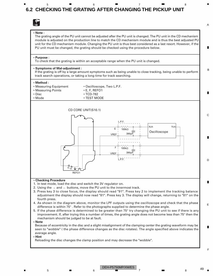
6.2 CHECKING THE GRATING AFTER CHANGING THE PICKUP UNIT
• Note :The grating angle of the PU unit cannot be adjusted after the PU unit is changed. The PU unit in the CD mechanism module is adjusted on the production line to match the CD mechanism module and is thus the best adjusted PU unit for the CD mechanism module. Changing the PU unit is thus best considered as a last resort. However, if the PU unit must be changed, the grating should be checked using the procedure below.
• Purpose :To check that the grating is within an acceptable range when the PU unit is changed.
• Symptoms of Mal-adjustment :If the grating is off by a large amount symptoms such as being unable to close tracking, being unable to perform track search operations, or taking a long time for track searching.
• Method :
• Measuring Equipment• Measuring Points
• Oscilloscope, Two L.P.F.• E, F, REFO1
• Disc • TCD-782• Mode • TEST MODE
• Checking Procedure1. In test mode, load the disc and switch the 3V regulator on.2. Using the → and ← buttons, move the PU unit to the innermost track.3. Press key 3 to close focus, the display should read "91". Press key 2 to implement the tracking balance adjustment the display should now read "81". Press key 3. The display will change, returning to "81" on the fourth press.4. As shown in the diagram above, monitor the LPF outputs using the oscilloscope and check that the phase difference is within 75° . Refer to the photographs supplied to determine the phase angle.5. If the phase difference is determined to be greater than 75° try changing the PU unit to see if there is any improvement. If, after trying this a number of times, the grating angle does not become less than 75° then the mechanism should be judged to be at fault.• NoteBecause of eccentricity in the disc and a slight misalignment of the clamping center the grating waveform may be seen to "wobble" ( the phase difference changes as the disc rotates). The angle specified above indicates the average angle.
• HintReloading the disc changes the clamp position and may decrease the "wobble".
100kΩ
390pF
100kΩ
390pF
E
VREF
F
VREF
Xch Ych
L.P.F.
L.P.F.
REFO1
F E
CD CORE UNIT(S10.1)
Oscilloscope
DEH-P5750MP/XM/ES 495 6 7 8
C
D
F
A
B
E
1 2 3 4
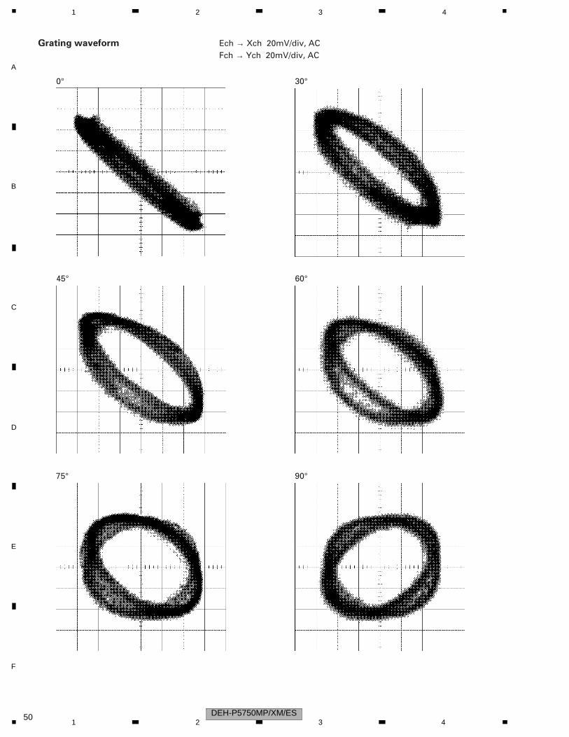
Grating waveform
45°
0°
75°
60°
30°
90°
Ech → Xch 20mV/div, ACFch → Ych 20mV/div, AC
DEH-P5750MP/XM/ES501 2 3 4
C
D
F
A
B
E
5 6 7 8
6.3 ERROR MODE
- Error Messages
Error is displayed with number for Error cause when CD is inoperative or stops with Error during operation.The purpose is to reduce nonsense calls from users as well as to assist all related analysis and repair for defects at service station.
(1) Basic Display Method
1) When CSMOD (CD mode area for system) is SERRORM, Error code will be written in DMIN (minutes area for display), DSEC (seconds area for display). The same data shall be written in DMIN and DSEC. DTNO is blank as usual.
2) Display Example of Head Unit
The following is about LCD display ability. xx is Error number.
8 digits 6 digits 4 digits
ERROR–xx ERR–xx E–xx
(2) Error Code List
No. Classification Contents Details • Cause
10 Electricity Carriage Home NG CRG can’t move to the inner.
CRG can’t move from the inner.
→ HOME SW failure, CRG movement failure.
11 Electricity Focus Search NG Focus can’t be caught.
→ Back of Disc / Severe dirt and vibration.
23 Disc File Format NG Contents are stored in an incompatible file format.
→ The contents in a CD-ROM disc inserted are recorded in a file format other than ISO9660 Level-1 and 2.
22 Disc Impossible to play There is no playable MP3 or WMA file present in a disc.
→ No MP3 or WMA file exists in a CD-ROM disc inserted.
17 Electricity Setup NG AGC protection doesn’t work, out of Focus soon.
→ Scratch on Disc/Severe dirt and vibration.
12 Electricity Spindle Lock NG Not spindle, lock. Wrong subcode (can’t read).
Subcode NG
RF-amp NG
→ Defective Spindle. Scratch and dirt on Disc. Intense vibration.
The appropriate gain of the RF amp cannot be obtained.
→ Defective spindle.
→ Blanc CD-R disc. Disc inserted upside down.
→ Scratched or dirty disc. Severe vibration. Abnormal CD signals.
30 Electricity Search Time Out Can’t reach the target address.
→ Defective CRG/tracking, or scratch on Disc.
→ All TRK Nos. In a disc inserted are specified as a track which should be skipped, in the track skip information.
44 Disc Impossible to play There is no playable TRK No. present in a disc.
50 Mecha Disc Load / Eject NG Disc loading/ejection cannot be complete.
→ Foreign objects entered into the mechanism. Disc caught in between during loading/ejection.
A0 System Power NG Power supply (VD) isn’t connected to the ground.
→ Defective SW transistor. Abnormal power (failed connector)
OR
Err–xx
Note : Error doesn’t display in mechanism only. (CD off causes mechanism off) If TOC can’t be read, error wouldn’t occur, but mechanism still continues its operation. The upper digits of error code is mainly classified by 3 kinds as follows: 1x: Setup related error, 3x: Search related error, Ax: Other errors.
DEH-P5750MP/XM/ES 515 6 7 8
C
D
F
A
B
E
1 2 3 4
6.4 SYSTEM MICROCOMPUTER TEST PROGRAM
- PCL outputIn the normal operation mode (with the detachable panel installed, the ACC switched ON, the standby mode cancelled), shift the TESTIN (Pin 86) terminal to H. The clock signal is output from the PCL terminal (Pin 37). The frequency of the clock signal is 312.500kHz that is one 32nd of the fundamental frequency.The clock signal should be 312.500kHz ± 13Hz.If the clock signal is out of the range, the X'tal (X601) should be replaced with new one.
DEH-P5750MP/XM/ES521 2 3 4
C
D
F
A
B
E
5 6 7 8
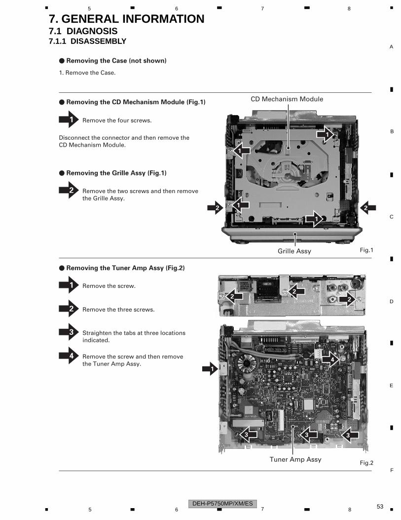
7. GENERAL INFORMATION7.1 DIAGNOSIS7.1.1 DISASSEMBLY
- Removing the CD Mechanism Module (Fig.1)
1
Fig.1
- Removing the Case (not shown)
Grille Assy
- Removing the Grille Assy (Fig.1)
1. Remove the Case.
CD Mechanism Module
1
1
1
1
Fig.2Tuner Amp Assy
- Removing the Tuner Amp Assy (Fig.2)
Remove the screw.1
Remove the four screws.
Disconnect the connector and then remove theCD Mechanism Module.
2 Remove the two screws and then remove the Grille Assy.
2 2
1
22
2
3 33
4
Remove the three screws.2
Straighten the tabs at three locations indicated.
3
Remove the screw and then remove the Tuner Amp Assy.
4
DEH-P5750MP/XM/ES 535 6 7 8
C
D
F
A
B
E
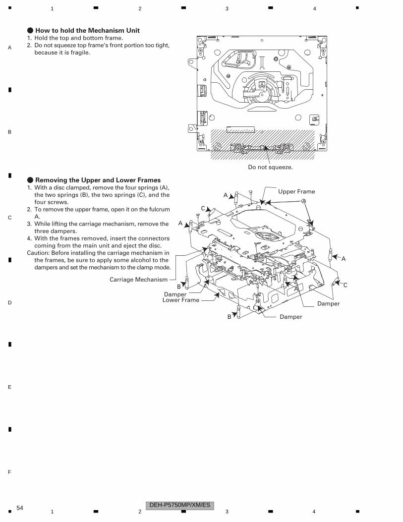
1 2 3 4
- How to hold the Mechanism Unit1. Hold the top and bottom frame.2. Do not squeeze top frame's front portion too tight, because it is fragile.
- Removing the Upper and Lower Frames1. With a disc clamped, remove the four springs (A), the two springs (B), the two springs (C), and the four screws.2. To remove the upper frame, open it on the fulcrum A.3. While lifting the carriage mechanism, remove the three dampers.4. With the frames removed, insert the connectors coming from the main unit and eject the disc.Caution: Before installing the carriage mechanism in the frames, be sure to apply some alcohol to the dampers and set the mechanism to the clamp mode.
Do not squeeze.
Lower FrameDamper
Carriage Mechanism
A
C
A
B
B
Damper
Damper
C
A
A
A
Upper Frame
DEH-P5750MP/XM/ES541 2 3 4
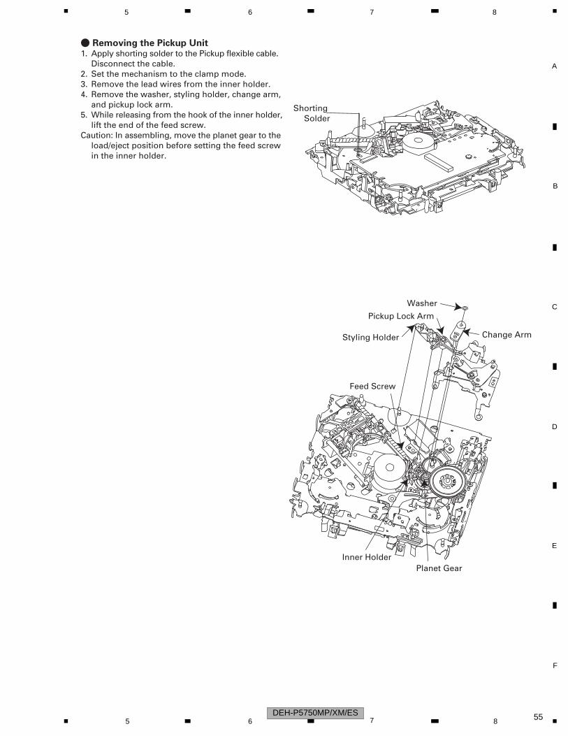
C
D
F
A
B
E
5 6 7 8
- Removing the Pickup Unit1. Apply shorting solder to the Pickup flexible cable. Disconnect the cable.2. Set the mechanism to the clamp mode.3. Remove the lead wires from the inner holder.4. Remove the washer, styling holder, change arm, and pickup lock arm.5. While releasing from the hook of the inner holder, lift the end of the feed screw.Caution: In assembling, move the planet gear to the load/eject position before setting the feed screw in the inner holder.
Shorting Solder
Planet Gear
Change Arm
Inner Holder
Styling Holder
Feed Screw
Washer
Pickup Lock Arm
DEH-P5750MP/XM/ES 555 6 7 8
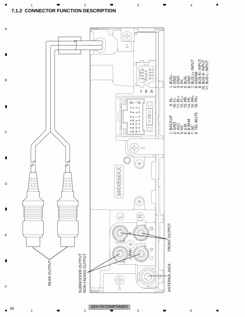
C
D
F
A
B
E
1 2 3 4
7.1.2 CONNECTOR FUNCTION DESCRIPTION
AN
TE
NN
A J
AC
KFR
ON
T O
UT
PU
T
SU
BW
OO
FER
OU
TP
UT
NO
N F
AD
ING
OU
TP
UT
1. B
US
+ 2
. GN
D 3
. GN
D 4
. NC
5. B
US
- 6
. GN
D 7
. BU
S L
+ IN
PU
T 8
. AS
EN
B 9
. BU
S R
+ IN
PU
T10
. BU
S R
- IN
PU
T11
. BU
S L
- IN
PU
T
RE
AR
OU
TP
UT
9. R
L-10
. FL-
11. R
L+12
. FL+
13. R
R-
14. F
R-
15. R
R+
16. F
R+
1. B
AC
KU
P2.
GN
D3.
AC
C4.
NC
5. IL
M6.
B.R
EM
7. N
C8.
TE
L M
UT
E
SW
F
1 0 A
1110
98
76
5
43
21
151
1311
97
53
162
1412
108
64
DEH-P5750MP/XM/ES561 2 3 4
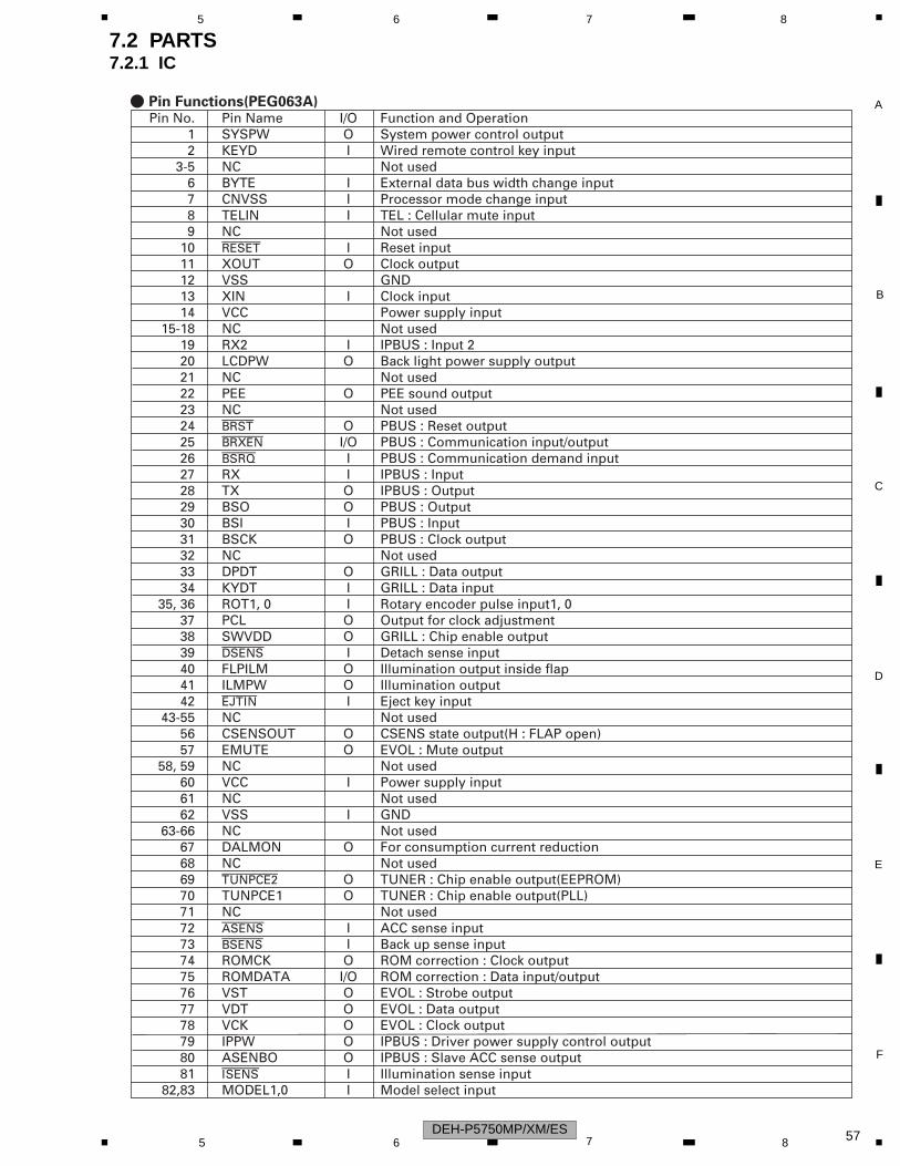
C
D
F
A
B
E
5 6 7 8
7.2 PARTS7.2.1 IC
- Pin Functions(PEG063A) Pin No. Pin Name I/O Function and Operation 1 SYSPW O System power control output 2 KEYD I Wired remote control key input 3-5 NC Not used 6 BYTE I External data bus width change input 7 CNVSS I Processor mode change input 8 TELIN I TEL : Cellular mute input 9 NC Not used 10 reset I Reset input 11 XOUT O Clock output 12 VSS GND 13 XIN I Clock input 14 VCC Power supply input 15-18 NC Not used 19 RX2 I IPBUS : Input 2 20 LCDPW O Back light power supply output 21 NC Not used 22 PEE O PEE sound output 23 NC Not used 24 brst O PBUS : Reset output 25 brxen I/O PBUS : Communication input/output 26 bsrq I PBUS : Communication demand input 27 RX I IPBUS : Input 28 TX O IPBUS : Output 29 BSO O PBUS : Output 30 BSI I PBUS : Input 31 BSCK O PBUS : Clock output 32 NC Not used 33 DPDT O GRILL : Data output 34 KYDT I GRILL : Data input 35, 36 ROT1, 0 I Rotary encoder pulse input1, 0 37 PCL O Output for clock adjustment 38 SWVDD O GRILL : Chip enable output 39 dsens I Detach sense input 40 FLPILM O Illumination output inside flap 41 ILMPW O Illumination output 42 ejtin I Eject key input 43-55 NC Not used 56 CSENSOUT O CSENS state output(H : FLAP open) 57 EMUTE O EVOL : Mute output 58, 59 NC Not used 60 VCC I Power supply input 61 NC Not used 62 VSS I GND 63-66 NC Not used 67 DALMON O For consumption current reduction 68 NC Not used 69 tunpce@ O TUNER : Chip enable output(EEPROM) 70 TUNPCE1 O TUNER : Chip enable output(PLL) 71 NC Not used 72 asens I ACC sense input 73 bsens I Back up sense input 74 ROMCK O ROM correction : Clock output 75 ROMDATA I/O ROM correction : Data input/output 76 VST O EVOL : Strobe output 77 VDT O EVOL : Data output 78 VCK O EVOL : Clock output 79 IPPW O IPBUS : Driver power supply control output 80 ASENBO O IPBUS : Slave ACC sense output 81 isens I Illumination sense input 82,83 MODEL1,0 I Model select input
DEH-P5750MP/XM/ES 575 6 7 8
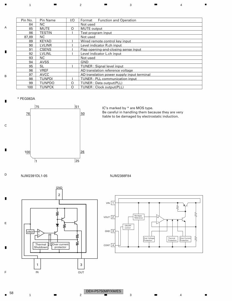
C
D
F
A
B
E
1 2 3 4
Pin No. Pin Name I/O Format Function and Operation 84 NC Not used 85 MUTE O MUTE output 86 TESTIN I Test program input 87,89 NC Not used 89 KEYAD I Wired remote control key input 90 LVLINR I Level indicator R.ch input 91 CSENS I Flap opening-and-closing sense input 92 LVLINL I Level indicator L.ch input 93 NC Not used 94 AVSS GND 95 SL I TUNER : Signal level input 96 VREF AD translation reference voltage 97 AVCC AD translation power supply input terminal 98 TUNPDI I TUNER : PLL communication input 99 TUNPDO O TUNER : Data output(PLL) 100 TUNPCK O TUNER : Clock output(PLL)
* PEG063A
NJM2391DL1-05
IC's marked by * are MOS type.Be careful in handling them because they are very liable to be damaged by electrostatic induction.
25
26
50
5175
76
100
1
NJM2388F84
IN OUT
GND
1 3
2
ThermalShutdown
Over currentprotector
VREF
+-
1
2
3
4
VIN
Bandgap ReferenceVOUT
GND
CONT
ON/OFF control
Over VoltageProtection
ThermalProtection
Over CurrentProtection
+-
DEH-P5750MP/XM/ES581 2 3 4
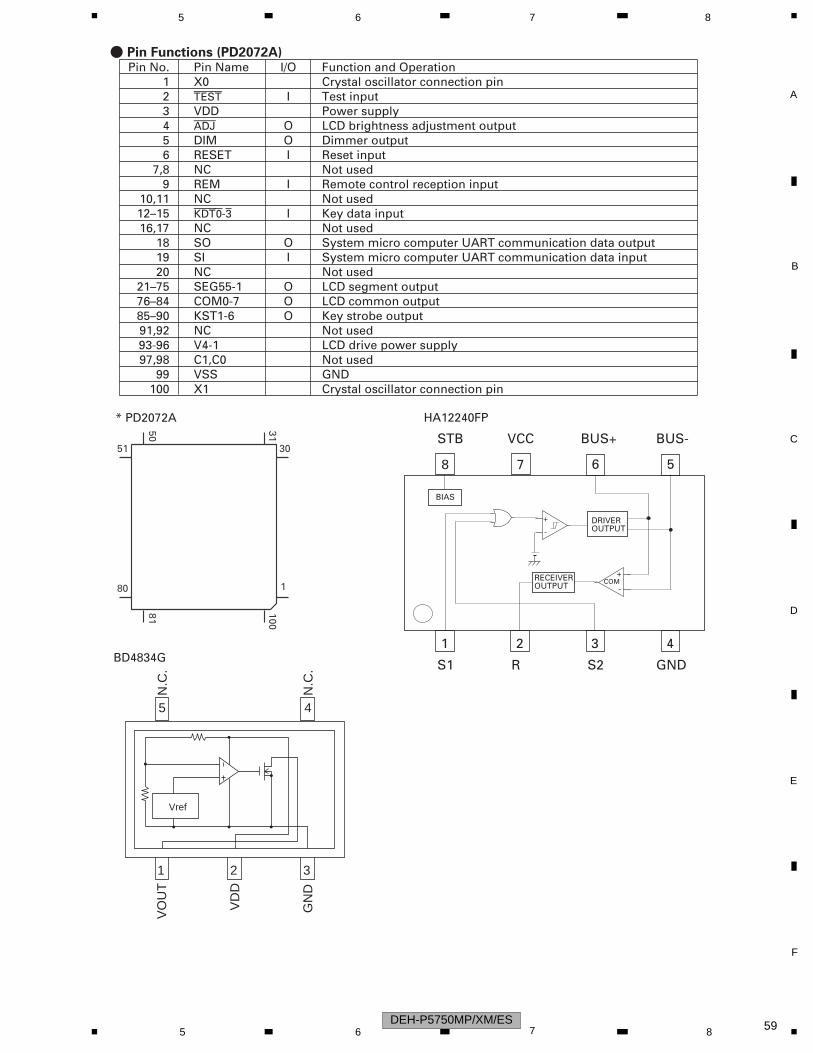
C
D
F
A
B
E
5 6 7 8
- Pin Functions (PD2072A)Pin No. Pin Name I/O Function and Operation
4DIM Dimmer output
2 test Test input
100 X1 Crystal oscillator connection pin
X0 Crystal oscillator connection pin
VDD Power supply
6NC Not used
O
O
16,17 NC Not used
NC Not used12–15 I
I
Key data input
SO O System micro computer UART communication data outputSI I System micro computer UART communication data inputNC Not usedSEG55-1 O LCD segment outputCOM0-7 O
RESET Reset inputI
O
I
LCD common outputKST1-6 Key strobe outputNC Not usedV4-1 LCD drive power supplyC1,C0 Not used
* PD2072A
30
3150
51
80
81 100
1
kdt0-3
1
3
5adj LCD brightness adjustment output
7,89 REM Remote control reception input
10,11
VSS GND99
181920
21–7576–8485–9091,9293-9697,98
1 2 3
VD
D
GN
D
5 4
VO
UT
N.C
.
N.C
.
Vref
BD4834G1 32
S1 R S2 GND
BUS-BUS+VCCSTB
4
5678
BIAS
DRIVEROUTPUT
+
-
-
+
COMRECEIVEROUTPUT
HA12240FP
DEH-P5750MP/XM/ES 595 6 7 8
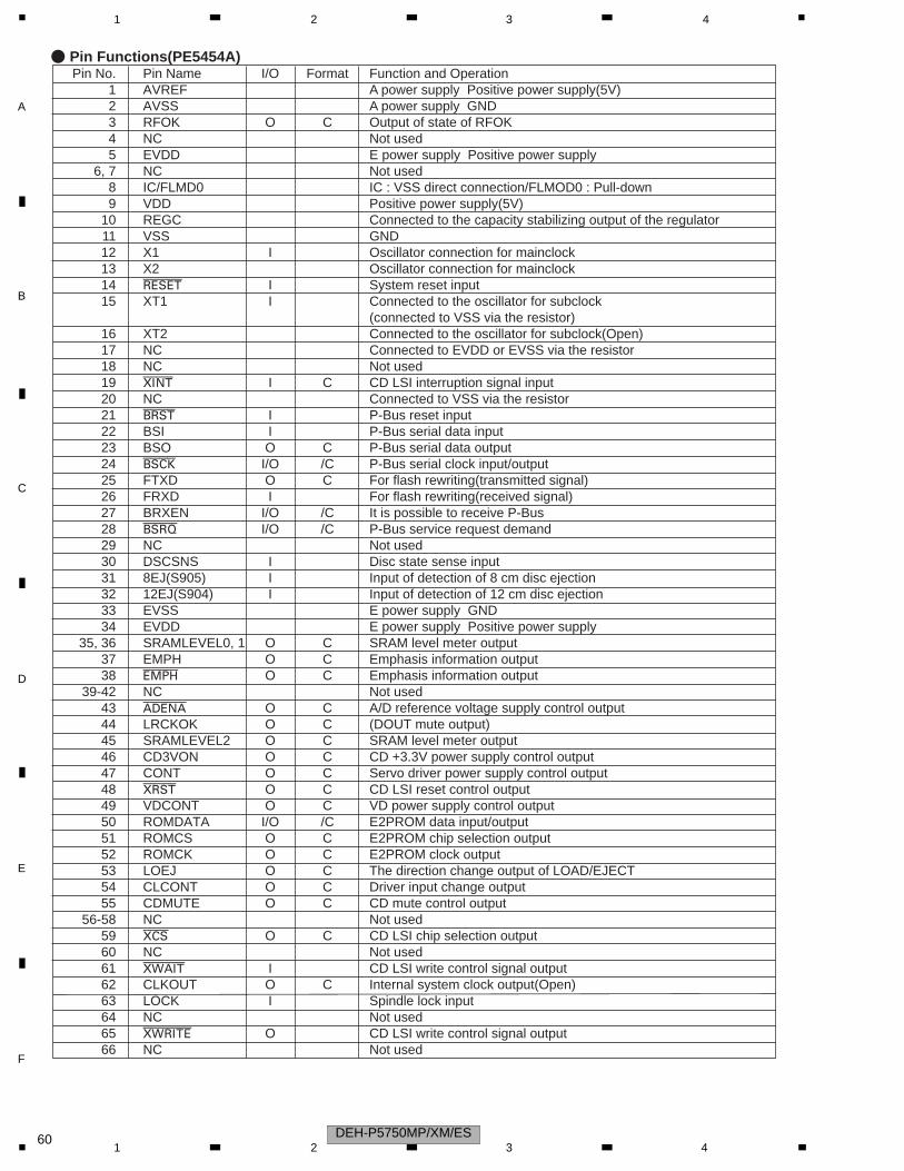
C
D
F
A
B
E
1 2 3 4
- Pin Functions(PE5454A) Pin No. Pin Name I/O Format Function and Operation 1 AVREF A power supply Positive power supply(5V) 2 AVSS A power supply GND 3 RFOK O C Output of state of RFOK 4 NC Not used 5 EVDD E power supply Positive power supply 6, 7 NC Not used 8 IC/FLMD0 IC : VSS direct connection/FLMOD0 : Pull-down 9 VDD Positive power supply(5V) 10 REGC Connected to the capacity stabilizing output of the regulator 11 VSS GND 12 X1 I Oscillator connection for mainclock 13 X2 Oscillator connection for mainclock 14 reset I System reset input 15 XT1 I Connected to the oscillator for subclock (connected to VSS via the resistor) 16 XT2 Connected to the oscillator for subclock(Open) 17 NC Connected to EVDD or EVSS via the resistor 18 NC Not used 19 xint I C CD LSI interruption signal input 20 NC Connected to VSS via the resistor 21 brst I P-Bus reset input 22 BSI I P-Bus serial data input 23 BSO O C P-Bus serial data output 24 bsck I/O /C P-Bus serial clock input/output 25 FTXD O C For flash rewriting(transmitted signal) 26 FRXD I For flash rewriting(received signal) 27 BRXEN I/O /C It is possible to receive P-Bus 28 bsrq I/O /C P-Bus service request demand 29 NC Not used 30 DSCSNS I Disc state sense input 31 8EJ(S905) I Input of detection of 8 cm disc ejection 32 12EJ(S904) I Input of detection of 12 cm disc ejection 33 EVSS E power supply GND 34 EVDD E power supply Positive power supply 35, 36 SRAMLEVEL0, 1 O C SRAM level meter output 37 EMPH O C Emphasis information output 38 emph O C Emphasis information output 39-42 NC Not used 43 adena O C A/D reference voltage supply control output 44 LRCKOK O C (DOUT mute output) 45 SRAMLEVEL2 O C SRAM level meter output 46 CD3VON O C CD +3.3V power supply control output 47 CONT O C Servo driver power supply control output 48 xrst O C CD LSI reset control output 49 VDCONT O C VD power supply control output 50 ROMDATA I/O /C E2PROM data input/output 51 ROMCS O C E2PROM chip selection output 52 ROMCK O C E2PROM clock output 53 LOEJ O C The direction change output of LOAD/EJECT 54 CLCONT O C Driver input change output 55 CDMUTE O C CD mute control output 56-58 NC Not used 59 xcs O C CD LSI chip selection output 60 NC Not used 61 xwait I CD LSI write control signal output 62 CLKOUT O C Internal system clock output(Open) 63 LOCK I Spindle lock input 64 NC Not used 65 xwrite O CD LSI write control signal output 66 NC Not used
DEH-P5750MP/XM/ES601 2 3 4
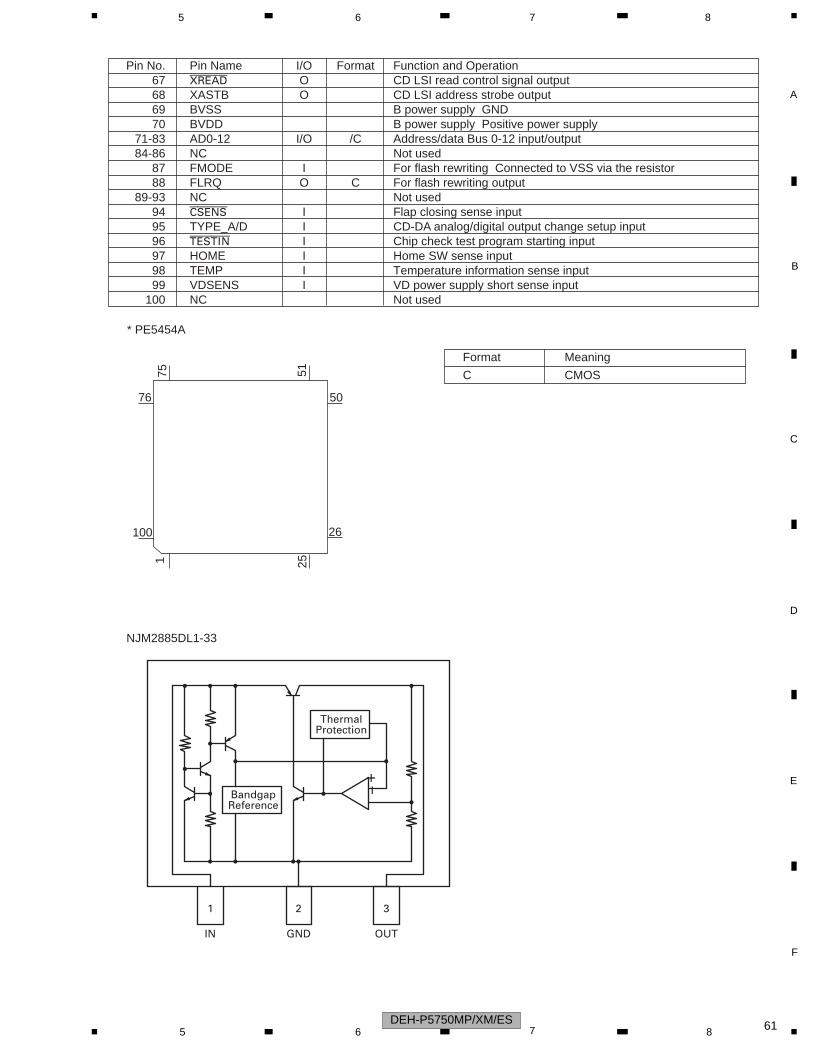
C
D
F
A
B
E
5 6 7 8
Pin No. Pin Name I/O Format Function and Operation 67 xread O CD LSI read control signal output 68 XASTB O CD LSI address strobe output 69 BVSS B power supply GND 70 BVDD B power supply Positive power supply 71-83 AD0-12 I/O /C Address/data Bus 0-12 input/output 84-86 NC Not used 87 FMODE I For flash rewriting Connected to VSS via the resistor 88 FLRQ O C For flash rewriting output 89-93 NC Not used 94 csens I Flap closing sense input 95 TYPE_A/D I CD-DA analog/digital output change setup input 96 testin I Chip check test program starting input 97 HOME I Home SW sense input 98 TEMP I Temperature information sense input 99 VDSENS I VD power supply short sense input 100 NC Not used
* PE5454A
25
26
50
5175
76
100
1
Format Meaning
C CMOS
IN
1
GND
2
OUT
3
BandgapReference
ThermalProtection
+-
NJM2885DL1-33
DEH-P5750MP/XM/ES 615 6 7 8
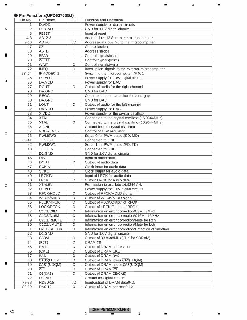
C
D
F
A
B
E
1 2 3 4
- Pin Functions(UPD63763GJ) Pin No. Pin Name I/O Function and Operation 1 D.VDD Power supply for digital circuits 2 D1.GND GND for 1.6V digital circuits 3 reset I Input of reset 4-8 AB12-8 I Address bus 12-8 from the microcomputer 9-16 AD7-0 I/O Address/data bus 7-0 to the microcomputer 17 cs I Chip selection 18 ASTB I Address strobe 19 read I Control signals(read) 20 write I Control signals(write) 21 wait O Control signals(wait) 22 INTQ O Interruption signals to the external microcomputer 23, 24 IFMODE0, 1 I Switching the microcomputer I/F 0, 1 25 D1.VDD Power supply for 1.6V digital circuits 26 DA.VDD Power supply for DAC 27 ROUT O Output of audio for the right channel 28 DA.GND GND for DAC 29 REGC Connected to the capacitor for band gap 30 DA.GND GND for DAC 31 LOUT O Output of audio for the left channel 32 DA.VDD Power supply for DAC 33 X.VDD Power supply for the crystal oscillator 34 XTAL I Connected to the crystal oscillator(16.9344MHz) 35 xtal O Connected to the crystal oscillator(16.9344MHz) 36 X.GND Ground for the crystal oscillator 37 VDDREG15 Control of 1.6V regulator 38 PWMSW0 I Setup 0 for PWM output(SD, MD) 39-41 TEST3-1 I Connected to GND 42 PWMSW1 I Setup 1 for PWM output(FD, TD) 43 TESTEN I Connected to GND 44 D1.GND GND for 1.6V digital circuits 45 DIN I Input of audio data 46 DOUT O Output of audio data 47 SCKIN I Clock input for audio data 48 SCKO O Clock output for audio data 49 LRCKIN I Input of LRCK for audio data 50 LRCK O Output LRCK for audio data 51 xtalen I Permission to oscillate 16.9344MHz 52 D1.VDD Power supply for 1.6V digital circuits 53 RFCK/HOLD O Output of RFCK/HOLD signal 54 WFCK/MIRR O Output of WFCK/MIRR signal 55 PLCK/RFOK O Output of PLCK/Output of RFOK 56 LOCK/RFOK O Output of LRCK/Output of RFOK 57 C1D1/C8M O Information on error correction/C8M : 8MHz 58 C1D2/C16M O Information on error correction/C16M : 16MHz 59 C2D1/RMUTE O Information on error correction/Mute for Rch 60 C2D2/LMUTE O Information on error correction/Mute for Lch 61 C2D3/SHOCK O Information on error correction/Detection of vibration 62 D1.GND GND for 1.6V digital circuits 63 C33M O Output of 33.8688MHz(CLK for SDRAM) 64 (rcs) O DRAM cs 65 RA11 O Output of DRAM address 11 66 (CKE) O Output of DRAM CKE 67 ras O Output of DRAM ras 68 cas)(LDQM) O Output of DRAM lower cas(LDQM) 69 cas!(UDQM) O Output of DRAM upper cas(UDQM) 70 we O Output of DRAM we 71 oe(cas) O Output of DRAM oe(cas) 72 D.GND Ground for digital circuits 73-88 RDB0-15 I/O Input/output of DRAM data0-15 89-99 RA0-10 O Output of DRAM address0-10
DEH-P5750MP/XM/ES621 2 3 4
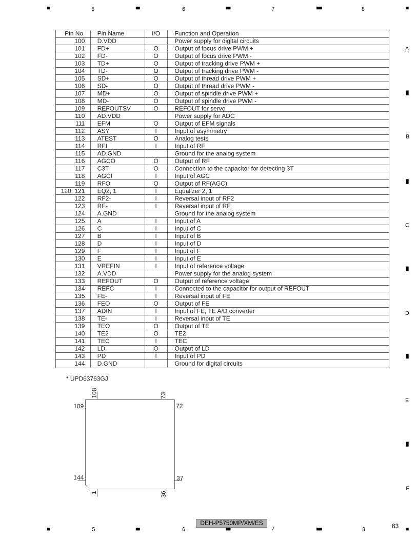
C
D
F
A
B
E
5 6 7 8
Pin No. Pin Name I/O Function and Operation 100 D.VDD Power supply for digital circuits 101 FD+ O Output of focus drive PWM + 102 FD- O Output of focus drive PWM - 103 TD+ O Output of tracking drive PWM + 104 TD- O Output of tracking drive PWM - 105 SD+ O Output of thread drive PWM + 106 SD- O Output of thread drive PWM - 107 MD+ O Output of spindle drive PWM + 108 MD- O Output of spindle drive PWM - 109 REFOUTSV O REFOUT for servo 110 AD.VDD Power supply for ADC 111 EFM O Output of EFM signals 112 ASY I Input of asymmetry 113 ATEST O Analog tests 114 RFI I Input of RF 115 AD.GND Ground for the analog system 116 AGCO O Output of RF 117 C3T O Connection to the capacitor for detecting 3T 118 AGCI I Input of AGC 119 RFO O Output of RF(AGC) 120, 121 EQ2, 1 I Equalizer 2, 1 122 RF2- I Reversal input of RF2 123 RF- I Reversal input of RF 124 A.GND Ground for the analog system 125 A I Input of A 126 C I Input of C 127 B I Input of B 128 D I Input of D 129 F I Input of F 130 E I Input of E 131 VREFIN I Input of reference voltage 132 A.VDD Power supply for the analog system 133 REFOUT O Output of reference voltage 134 REFC I Connected to the capacitor for output of REFOUT 135 FE- I Reversal input of FE 136 FEO O Output of FE 137 ADIN I Input of FE, TE A/D converter 138 TE- I Reversal input of TE 139 TEO O Output of TE 140 TE2 O TE2 141 TEC I TEC 142 LD O Output of LD 143 PD I Input of PD 144 D.GND Ground for digital circuits
* UPD63763GJ
72
73108
109
36
37
1
144
DEH-P5750MP/XM/ES 635 6 7 8
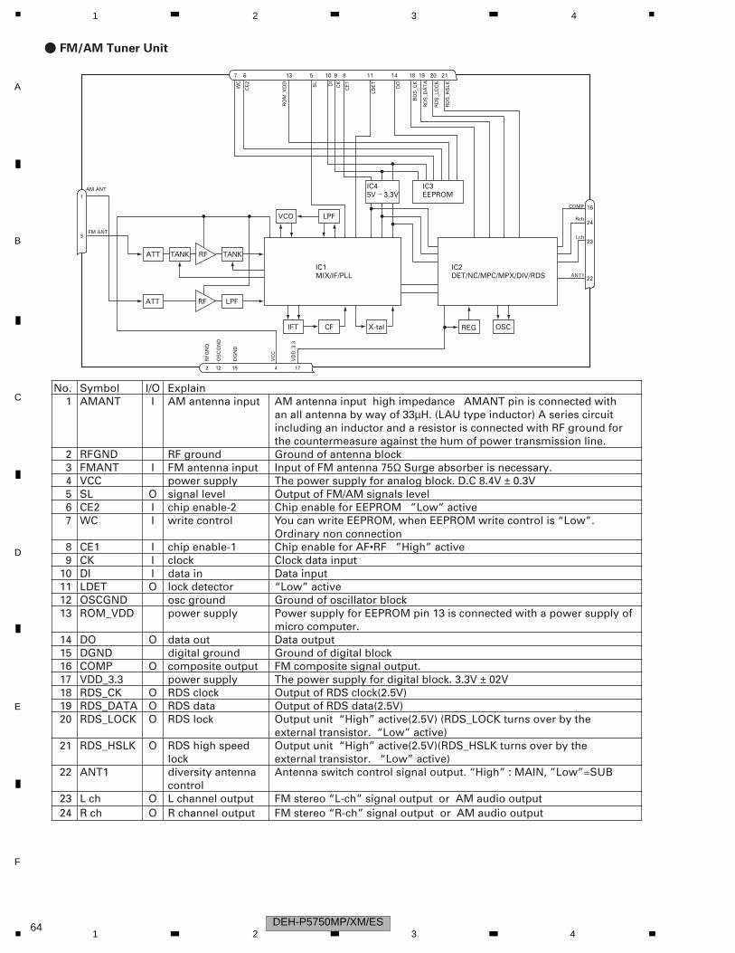
C
D
F
A
B
E
1 2 3 4
FM ANT
RFG
ND
OS
CG
ND
DG
ND
VC
C
VD
D_3
.3
WC
CE
2
RO
M_V
DD SL DI
CK
CE
1
LDE
T
DO
RD
S_C
K
RD
S_D
AT
A
RD
S_L
OC
K
RD
S_H
SLK
7 13 5 10 8 11 14 18 19 20 21
1
3
2 12 15 4 17
AM ANT
16
23
COMP
Lch
24Rch
22ANT1
6 9
IC45V 3.3V
IC3EEPROM
IC2DET/NC/MPC/MPX/DIV/RDS
REG OSCX-talCFIFT
LPF
TANK
RF
RFTANK
ATT
ATT
LPFVCO
IC1MIX/IF/PLL
←
No. Symbol I/O Explain1 AMANT I AM antenna input AM antenna input high impedance AMANT pin is connected with
an all antenna by way of 33µH. (LAU type inductor) A series circuit including an inductor and a resistor is connected with RF ground for the countermeasure against the hum of power transmission line.
2 RFGND RF ground Ground of antenna block3 FMANT I FM antenna input Input of FM antenna 75Ω Surge absorber is necessary.4 VCC power supply The power supply for analog block. D.C 8.4V ± 0.3V5 SL signal level Output of FM/AM signals level6 CE2 I
Ichip enable-2 Chip enable for EEPROM ”Low” active
7 WC write control You can write EEPROM, when EEPROM write control is “Low”.Ordinary non connection
8 CE1 II
chip enable-1 Chip enable for AF•RF ”High” active9 CK clock Clock data input
10 DI I data in Data input11 LDET O lock detector “Low” active12 OSCGND osc ground Ground of oscillator block13 ROM_VDD power supply Power supply for EEPROM pin 13 is connected with a power supply of
micro computer.14 DO O
O
data out Data output15 DGND digital ground Ground of digital block16 COMP composite output FM composite signal output.17 VDD_3.3 power supply The power supply for digital block. 3.3V ± 02V18 RDS_CK O RDS clock Output of RDS clock(2.5V)19 RDS_DATA O RDS data Output of RDS data(2.5V)20 RDS_LOCK O
O
O
RDS lock Output unit “High” active(2.5V) (RDS_LOCK turns over by the external transistor. “Low” active)
21 RDS_HSLK RDS high speed lock
Output unit “High” active(2.5V)(RDS_HSLK turns over by the external transistor. “Low” active)
22 ANT1 diversity antenna control
Antenna switch control signal output. “High” : MAIN, ”Low”=SUB
23 L ch O L channel output FM stereo “L-ch” signal output or AM audio output24 R ch O R channel output FM stereo “R-ch” signal output or AM audio output
- FM/AM Tuner Unit
DEH-P5750MP/XM/ES641 2 3 4
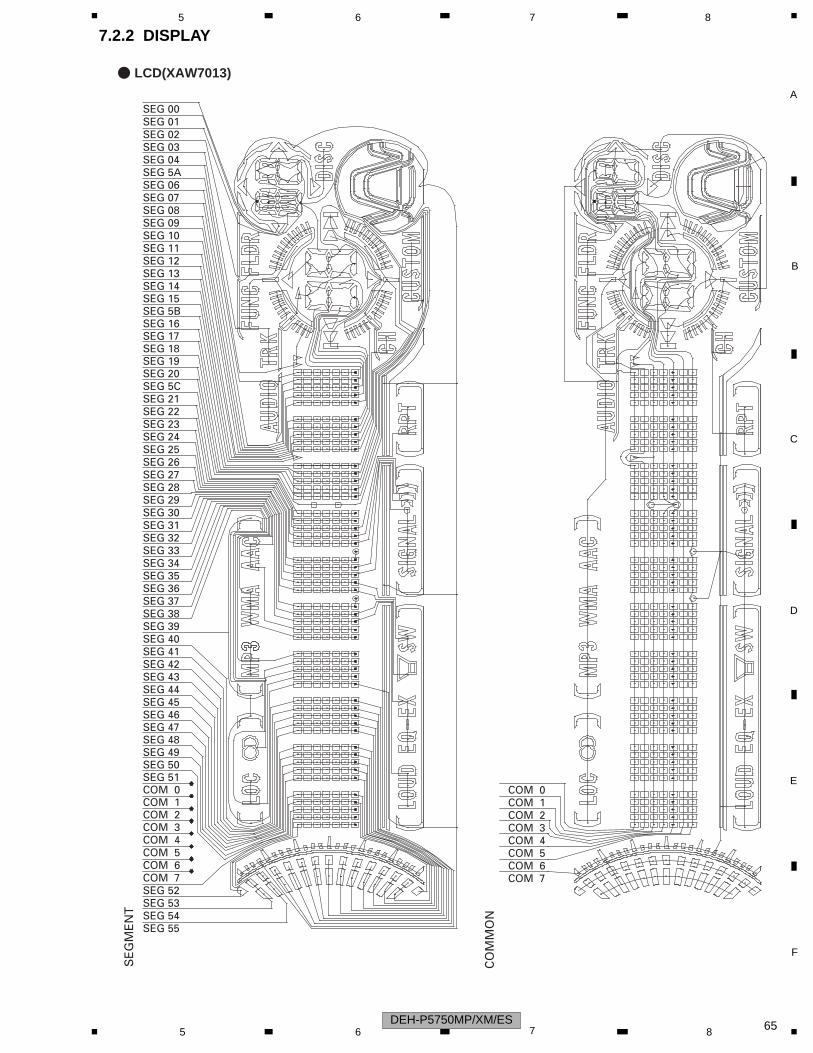
C
D
F
A
B
E
5 6 7 8
7.2.2 DISPLAY
- LCD(XAW7013)
CO
MM
ON
SE
GM
EN
T
SEG 00SEG 01SEG 02SEG 03SEG 04SEG 5ASEG 06SEG 07SEG 08SEG 09SEG 10SEG 11SEG 12SEG 13SEG 14SEG 15SEG 5BSEG 16SEG 17SEG 18SEG 19SEG 20SEG 5CSEG 21SEG 22SEG 23SEG 24SEG 25SEG 26SEG 27SEG 28SEG 29SEG 30SEG 31SEG 32SEG 33SEG 34SEG 35SEG 36SEG 37SEG 38SEG 39SEG 40SEG 41SEG 42SEG 43SEG 44SEG 45SEG 46SEG 47SEG 48SEG 49SEG 50SEG 51COM 0COM 1COM 2COM 3COM 4COM 5COM 6COM 7SEG 52SEG 53SEG 54SEG 55
COM 0COM 1COM 2COM 3COM 4COM 5COM 6COM 7
DEH-P5750MP/XM/ES 655 6 7 8
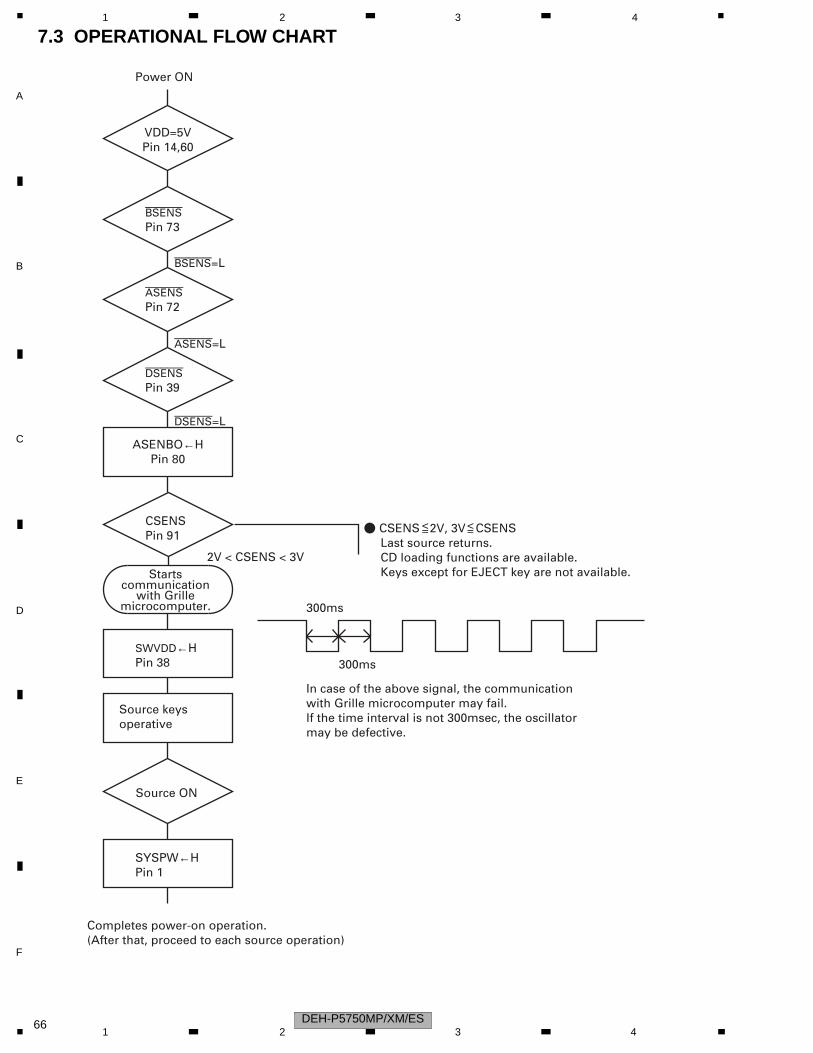
C
D
F
A
B
E
1 2 3 4
7.3 OPERATIONAL FLOW CHART
VDD=5VPin 14,60
ASENBO←HPin 80
Power ON
bsens=L
asens=L
dsens=L
bsensPin 73
asensPin 72
dsensPin 39
SWVDD←HPin 38
Source keys operative
Completes power-on operation.(After that, proceed to each source operation)
SYSPW←HPin 1
Startscommunication
with Grillemicrocomputer.
Source ON
300ms
300ms
In case of the above signal, the communication with Grille microcomputer may fail.If the time interval is not 300msec, the oscillator may be defective.
CSENSPin 91
2V < CSENS < 3V
- CSENS 2V, 3V CSENS Last source returns. CD loading functions are available. Keys except for EJECT key are not available.
< <= =
DEH-P5750MP/XM/ES661 2 3 4
C
D
F
A
B
E
5 6 7 8
7.4 CLEANING
Before shipping out the product, be sure to clean the following portions by using the prescribed cleaning tools:
Portions to be cleaned Cleaning tools
CD pickup lenses Cleaning liquid : GEM1004
Cleaning paper : GED-008
DEH-P5750MP/XM/ES 675 6 7 8
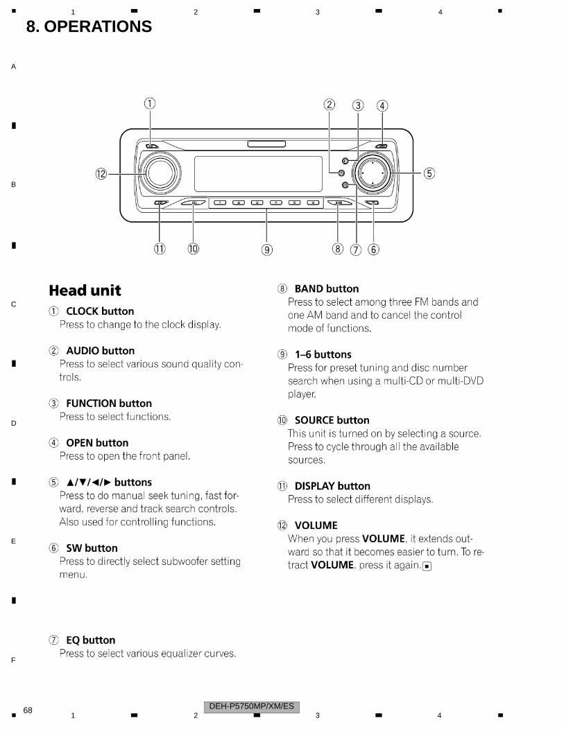
C
D
F
A
B
E
1 2 3 4
8. OPERATIONS
DEH-P5750MP/XM/ES681 2 3 4
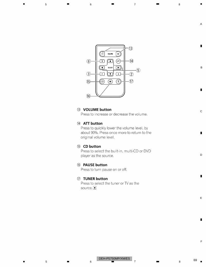
C
D
F
A
B
E
5 6 7 8
DEH-P5750MP/XM/ES 695 6 7 8
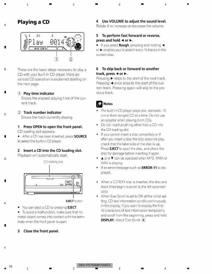
C
D
F
A
B
E
1 2 3 4
DEH-P5750MP/XM/ES701 2 3 4

C
D
F
A
B
E
5 6 7 8
DEH-P5750MP/XM/ES 715 6 7 8
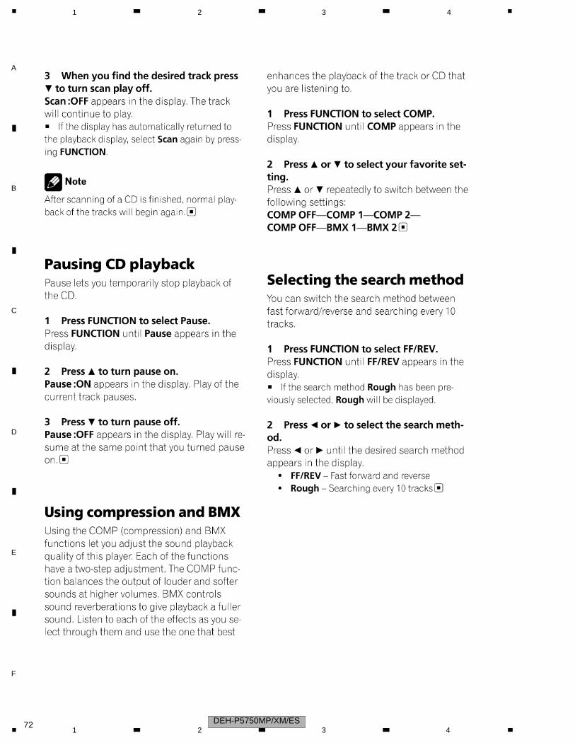
C
D
F
A
B
E
1 2 3 4
DEH-P5750MP/XM/ES721 2 3 4
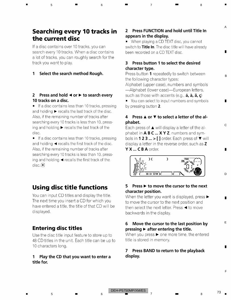
C
D
F
A
B
E
5 6 7 8
DEH-P5750MP/XM/ES 735 6 7 8
C
D
F
A
B
E
1 2 3 4
DEH-P5750MP/XM/ES741 2 3 4
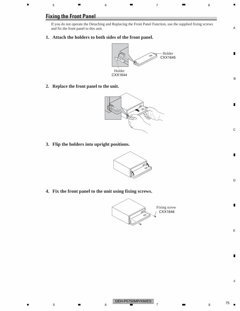
C
D
F
A
B
E
5 6 7 8
Fixing the Front PanelIf you do not operate the Detaching and Replacing the Front Panel Function, use the supplied fixing screwsand fix the front panel to this unit.
1. Attach the holders to both sides of the front panel.
2. Replace the front panel to the unit.
3. Flip the holders into upright positions.
4. Fix the front panel to the unit using fixing screws.
Fixing screw
HolderCXX1644
HolderCXX1645
CXX1646
DEH-P5750MP/XM/ES 755 6 7 8
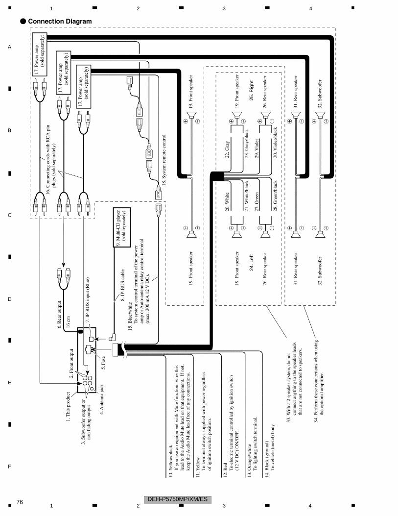
C
D
F
A
B
E
1 2 3 4
DEH-P5750MP/XM/ES761 2 3 4
C
D
F
A
B
E
5 6 7 8
DEH-P5750MP/XM/ES 775 6 7 8
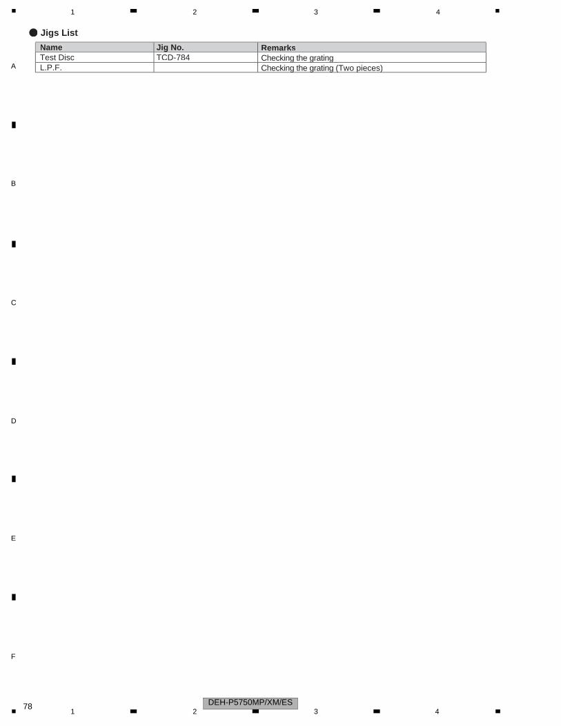
C
D
F
A
B
E
1 2 3 4
- Jigs List
Test DiscL.P.F.
TCD-784 Checking the gratingg g gChecking the grating g g g (Two pieces)( )
Name Jig No. Remarks
DEH-P5750MP/XM/ES781 2 3 4