Embed Size (px)
Citation preview
8/18/2019 Piezoresistive sensors-11-01819
http://slidepdf.com/reader/full/piezoresistive-sensors-11-01819 1/28
Sensors 2011, 11, 1819-1846; doi:10.3390/s110201819
sensorsISSN 1424-8220
www.mdpi.com/journal/sensors
Article
High-Performance Piezoresistive MEMS Strain Sensor with
Low Thermal Sensitivity
Ahmed A. S. Mohammed1,
*, Walied A. Moussa1 and
Edmond Lou
2
1 Mechanical Engineering Department, University of Alberta, Edmonton, AB, T6G 2G8, Canada;
E-Mail: [email protected] Department of Electrical and Computer Engineering, University of Alberta, Edmonton, AB, T6G
2V4, Canada; E-Mail: [email protected]
* Author to whom correspondence should be addressed; E-Mail: [email protected];
Tel.: +1-780-868-5824; Fax: +1-780-492-2200.
Received: 9 December 2010; in revised form: 18 January 2011 / Accepted: 20 January 2011 /
Published: 31 January 2011
Abstract: This paper presents the experimental evaluation of a new piezoresistive MEMS
strain sensor. Geometric characteristics of the sensor silicon carrier have been employed to
improve the sensor sensitivity. Surface features or trenches have been introduced in the
vicinity of the sensing elements. These features create stress concentration regions (SCRs)
and as a result, the strain/stress field was altered. The improved sensing sensitivity
compensated for the signal loss. The feasibility of this methodology was proved in a
previous work using Finite Element Analysis (FEA). This paper provides the experimental
part of the previous study. The experiments covered a temperature range from −50 °C to
+50 °C. The MEMS sensors are fabricated using five different doping concentrations. FEA
is also utilized to investigate the effect of material properties and layer thickness of the
bonding adhesive on the sensor response. The experimental findings are compared to the
simulation results to guide selection of bonding adhesive and installation procedure.
Finally, FEA was used to analyze the effect of rotational/alignment errors.
Keywords: strain sensor; piezoresistive; MEMS; silicon
OPEN ACCESS

8/18/2019 Piezoresistive sensors-11-01819
http://slidepdf.com/reader/full/piezoresistive-sensors-11-01819 2/28
Sensors 2011, 11 1820
1. Introduction
New advances in the field of Micro Electro Mechanical Systems (MEMS) have broadened
considerably the applications of these devices [1-3]. MEMS technology has also enabled the
miniaturization of the devices, and a typical MEMS sensor is at least one order of magnitude smallercompared to a conventional sensor that is used to measure the same quantity. Consequently, MEMS
devices can be patch-fabricated, which offers a high potential for cost reduction per unit. Moreover,
proper design can solve some problems related to power consumption, while providing improved
performance characteristics, such as accuracy, sensitivity and resolution.
Different sensing phenomena have been explored to develop MEMS sensors. These phenomena
include modulation of optical [4-6], capacitive [7,8], piezoelectric [9], frequency shift [10] and
piezoresistive properties [11-15]. Piezoresistive transduction has proved to have better performance
compared to other sensing physics [16-18]. Moreover, the corresponding devices can overcome
technical challenges related to chip integration; however, the response of piezoresistive devices undervarying temperature conditions has limited their applications. Therefore, during the design and
implementation of MEMS piezoresistive sensors, these shortcomings have to be considered.
It is well known that increasing dopant concentration reduces the sensor thermal drift [19-32] by
stabilizing the values of the piezoresistive coefficients. On the other hand, the increase in dopant
concentration also decreases the sensor sensitivity significantly. Another limitation during the application
of the MEMS strain sensors is the signal loss resulted from the stiffness discontinuity when mechanical
strain transmits through different structural layers, e.g., silicon carrier, bonding layer, etc. [11]. To
account for this strain field alteration, multi-stage calibration and characterization processes have to be
developed. In this sense, Finite Element Analysis (FEA) provides a reliable tool to carry out the
required parametric studies in order to optimize the sensor performance.
In this work, a new piezoresistive MEMS strain sensor is introduced. The developed MEMS-based
sensor has better performance characteristics compared to conventional thin-foil strain gauges, which
demonstrates it as a potential candidate in structural health monitoring (SHM) applications. The chips
incorporate piezoresistive sensing elements to measure mechanical strain via the observed changes in
their resistivity or mobility. Five different doping concentrations were studied to cover low, medium
and high doping levels. The fabricated chips were characterized over a temperature range from −50 °C
to +50 °C. The effect of both geometrical and microfabrication parameters on the output signal
strength was investigated.
The application range of the sensor is mainly restricted by both the electrical and mechanical
properties of silicon crystal. single crystal silicon has better mechanical properties compared to other
sensing materials [33-35]. FEA software was employed to investigate the potential rotational errors
that can occur during the sensor installation and fabrication. The strain sensing chips were designed
and prototyped bearing in mind flip chip packaging scheme, which permits subsequent integration with
components of SHM systems. This work confirmed the feasibility of using high doping concentrations
to realize high-performance piezoresistive MEMS sensors with acceptable sensitivity and stable
thermal behavior.
8/18/2019 Piezoresistive sensors-11-01819
http://slidepdf.com/reader/full/piezoresistive-sensors-11-01819 3/28
Sensors 2011, 11 1821
2. Sensor Design and Modeling
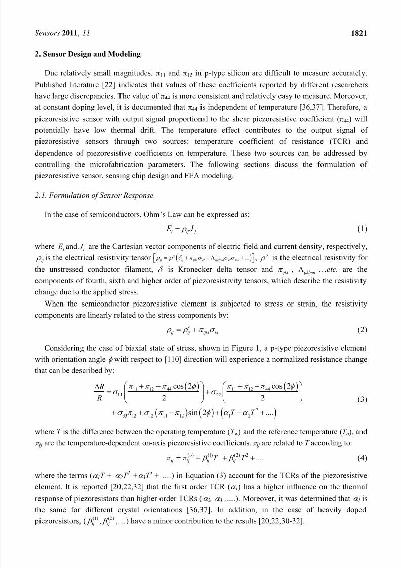
Due relatively small magnitudes, 11 and 12 in p-type silicon are difficult to measure accurately.
Published literature [22] indicates that values of these coefficients reported by different researchers
have large discrepancies. The value of 44 is more consistent and relatively easy to measure. Moreover,at constant doping level, it is documented that 44 is independent of temperature [36,37]. Therefore, a
piezoresistive sensor with output signal proportional to the shear piezoresistive coefficient (44) will
potentially have low thermal drift. The temperature effect contributes to the output signal of
piezoresistive sensors through two sources: temperature coefficient of resistance (TCR) and
dependence of piezoresistive coefficients on temperature. These two sources can be addressed by
controlling the microfabrication parameters. The following sections discuss the formulation of
piezoresistive sensor, sensing chip design and FEA modeling.
2.1. Formulation of Sensor Response
In the case of semiconductors, Ohm’s Law can be expressed as:
i ij j E J (1)
wherei
E andi J are the Cartesian vector components of electric field and current density, respectively,
ij is the electrical resistivity tensor ...o
ij ij ijkl kl ijklmn kl mn , o is the electrical resistivity for
the unstressed conductor filament, is Kronecker delta tensor andijkl ,
ijklmn …etc. are the
components of fourth, sixth and higher order of piezoresistivity tensors, which describe the resistivity
change due to the applied stress.
When the semiconductor piezoresistive element is subjected to stress or strain, the resistivity
components are linearly related to the stress components by:
o
ij ij ijkl kl (2)
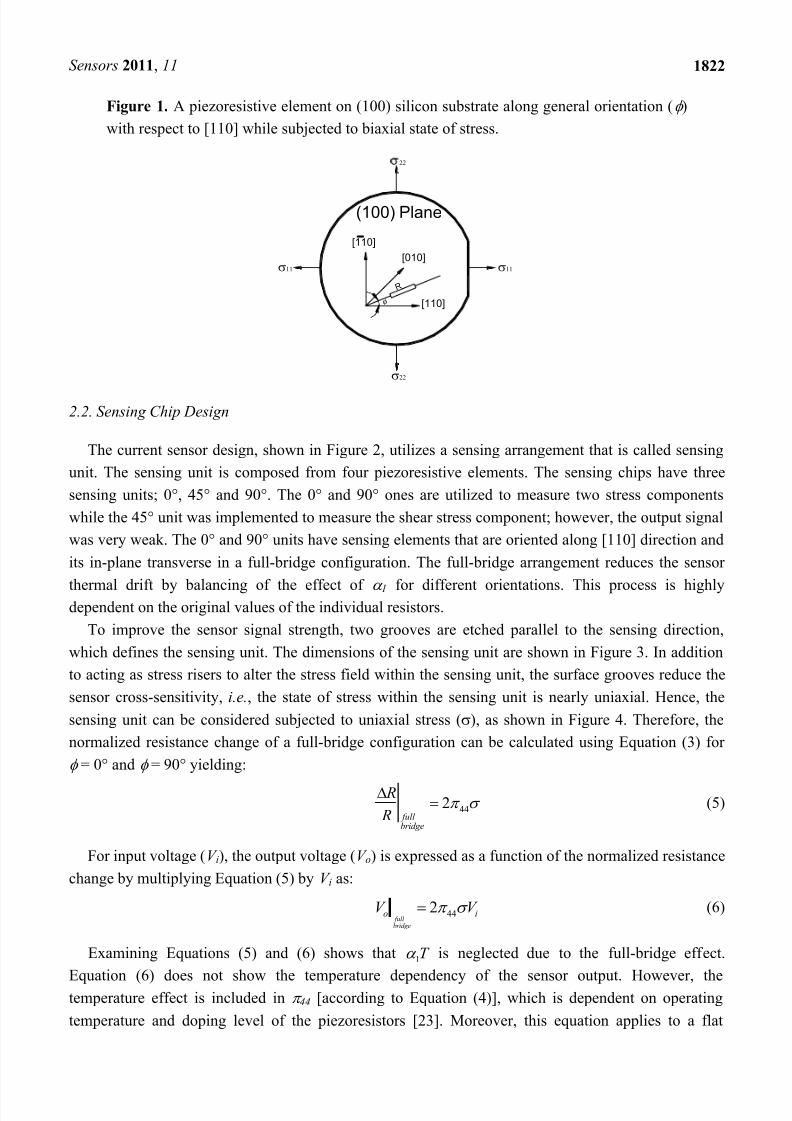
Considering the case of biaxial state of stress, shown in Figure 1, a p-type piezoresistive element
with orientation angle with respect to [110] direction will experience a normalized resistance change
that can be described by:
11 12 44 11 12 44
11 22
2
33 12 12 11 12 1 2
cos 2 cos 2
2 2
sin 2 ....
R
R
T T
(3)
where T is the difference between the operating temperature (T w) and the reference temperature (T o), and
ij are the temperature-dependent on-axis piezoresistive coefficients. ij are related to T according to:
( ) (1) (2) 2 ....o
ij i j ij ijT T (4)
where the terms ( 1T + 2T 2 + 3T 3 + ….) in Equation (3) account for the TCRs of the piezoresistive
element. It is reported [20,22,32] that the first order TCR ( 1) has a higher influence on the thermal
response of piezoresistors than higher order TCRs ( 2 , 3 ,….). Moreover, it was determined that 1 isthe same for different crystal orientations [36,37]. In addition, in the case of heavily doped
piezoresistors, ( (1)
ij , (2 )
ij ,…) have a minor contribution to the results [20,22,30-32].
8/18/2019 Piezoresistive sensors-11-01819
http://slidepdf.com/reader/full/piezoresistive-sensors-11-01819 4/28
Sensors 2011, 11 1822
Figure 1. A piezoresistive element on (100) silicon substrate along general orientation ( )
with respect to [110] while subjected to biaxial state of stress.
R
[010]
[110]
[110]
(100) Plane
2.2. Sensing Chip Design
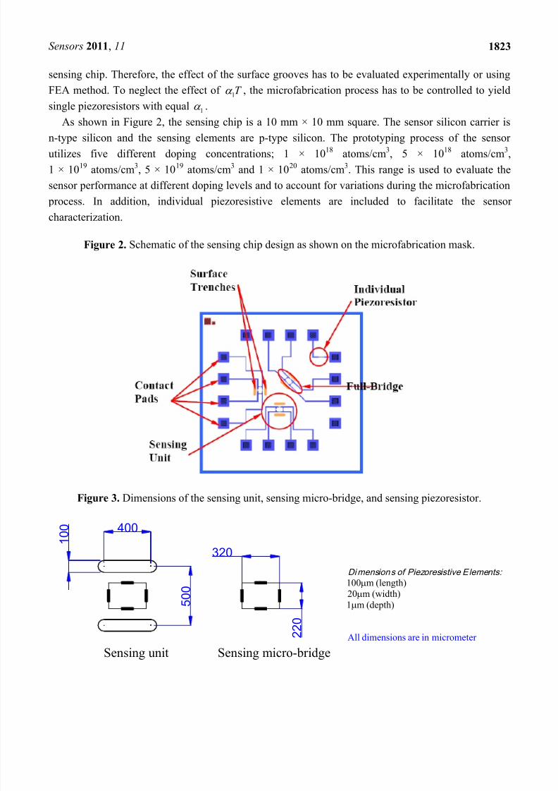
The current sensor design, shown in Figure 2, utilizes a sensing arrangement that is called sensing
unit. The sensing unit is composed from four piezoresistive elements. The sensing chips have three
sensing units; 0°, 45° and 90°. The 0° and 90° ones are utilized to measure two stress components
while the 45° unit was implemented to measure the shear stress component; however, the output signal
was very weak. The 0° and 90° units have sensing elements that are oriented along [110] direction and
its in-plane transverse in a full-bridge configuration. The full-bridge arrangement reduces the sensor
thermal drift by balancing of the effect of 1 for different orientations. This process is highlydependent on the original values of the individual resistors.
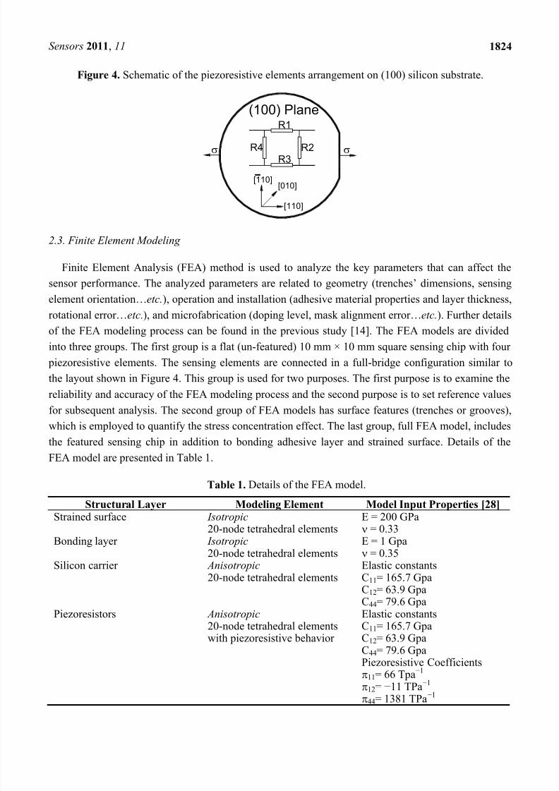
To improve the sensor signal strength, two grooves are etched parallel to the sensing direction,
which defines the sensing unit. The dimensions of the sensing unit are shown in Figure 3. In addition
to acting as stress risers to alter the stress field within the sensing unit, the surface grooves reduce the
sensor cross-sensitivity, i.e., the state of stress within the sensing unit is nearly uniaxial. Hence, the
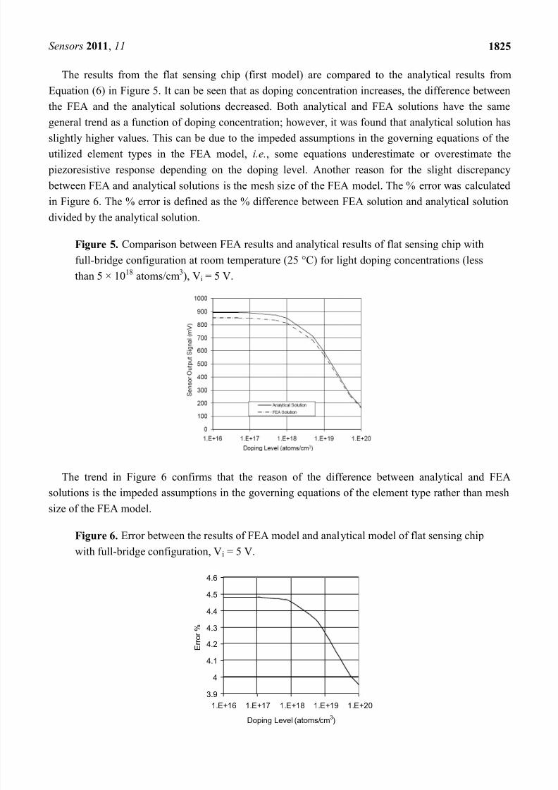
sensing unit can be considered subjected to uniaxial stress (), as shown in Figure 4. Therefore, the
normalized resistance change of a full-bridge configuration can be calculated using Equation (3) for
= 0° and = 90° yielding:
442 full bridge
R
R
(5)
For input voltage (V i), the output voltage (V o) is expressed as a function of the normalized resistance
change by multiplying Equation (5) by V i as:
442 full bridge
o iV V (6)
Examining Equations (5) and (6) shows that1T is neglected due to the full-bridge effect.
Equation (6) does not show the temperature dependency of the sensor output. However, thetemperature effect is included in 44 [according to Equation (4)], which is dependent on operating
temperature and doping level of the piezoresistors [23]. Moreover, this equation applies to a flat
8/18/2019 Piezoresistive sensors-11-01819
http://slidepdf.com/reader/full/piezoresistive-sensors-11-01819 5/28
Sensors 2011, 11 1823
sensing chip. Therefore, the effect of the surface grooves has to be evaluated experimentally or using
FEA method. To neglect the effect of1T , the microfabrication process has to be controlled to yield
single piezoresistors with equal1 .
As shown in Figure 2, the sensing chip is a 10 mm × 10 mm square. The sensor silicon carrier is
n-type silicon and the sensing elements are p-type silicon. The prototyping process of the sensorutilizes five different doping concentrations; 1 × 10¹⁸ atoms/cm3, 5 × 10¹⁸ atoms/cm3,
1 × 10¹⁹ atoms/cm3, 5 × 10¹⁹ atoms/cm3 and 1 × 10²⁰ atoms/cm3. This range is used to evaluate the
sensor performance at different doping levels and to account for variations during the microfabrication
process. In addition, individual piezoresistive elements are included to facilitate the sensor
characterization.
Figure 2. Schematic of the sensing chip design as shown on the microfabrication mask.
Figure 3. Dimensions of the sensing unit, sensing micro-bridge, and sensing piezoresistor.
1 0 0
5 0 0
2 2 0
Sensing unit Sensing micro-bridge
400
320Dimensions of Piezoresistive Elements:
100m (length)
20m (width)
1m (depth)
All dimensions are in micrometer
8/18/2019 Piezoresistive sensors-11-01819
http://slidepdf.com/reader/full/piezoresistive-sensors-11-01819 6/28
Sensors 2011, 11 1824
Figure 4. Schematic of the piezoresistive elements arrangement on (100) silicon substrate.
R1
R3R2R4
[010][110]
[110]
(100) Plane
2.3. Finite Element Modeling
Finite Element Analysis (FEA) method is used to analyze the key parameters that can affect the
sensor performance. The analyzed parameters are related to geometry (trenches’ dimensions, sensing
element orientation…etc.), operation and installation (adhesive material properties and layer thickness,
rotational error …etc.), and microfabrication (doping level, mask alignment error…etc.). Further details
of the FEA modeling process can be found in the previous study [14]. The FEA models are divided
into three groups. The first group is a flat (un-featured) 10 mm × 10 mm square sensing chip with four
piezoresistive elements. The sensing elements are connected in a full-bridge configuration similar to
the layout shown in Figure 4. This group is used for two purposes. The first purpose is to examine the
reliability and accuracy of the FEA modeling process and the second purpose is to set reference values
for subsequent analysis. The second group of FEA models has surface features (trenches or grooves),which is employed to quantify the stress concentration effect. The last group, full FEA model, includes
the featured sensing chip in addition to bonding adhesive layer and strained surface. Details of the
FEA model are presented in Table 1.
Table 1. Details of the FEA model.
Structural Layer Modeling Element Model Input Properties [28]Strained surface Isotropic
20-node tetrahedral elementsE = 200 GPa = 0.33
Bonding layer Isotropic
20-node tetrahedral elements
E = 1 Gpa
= 0.35Silicon carrier Anisotropic
20-node tetrahedral elementsElastic constantsC11= 165.7 GpaC12= 63.9 GpaC44= 79.6 Gpa
Piezoresistors Anisotropic20-node tetrahedral elementswith piezoresistive behavior
Elastic constantsC11= 165.7 GpaC12= 63.9 GpaC44= 79.6 GpaPiezoresistive Coefficients11= 66 Tpa−1
12= −11 TPa−1
44= 1381 TPa−1
8/18/2019 Piezoresistive sensors-11-01819
http://slidepdf.com/reader/full/piezoresistive-sensors-11-01819 7/28
Sensors 2011, 11 1825
The results from the flat sensing chip (first model) are compared to the analytical results from
Equation (6) in Figure 5. It can be seen that as doping concentration increases, the difference between
the FEA and the analytical solutions decreased. Both analytical and FEA solutions have the same
general trend as a function of doping concentration; however, it was found that analytical solution has
slightly higher values. This can be due to the impeded assumptions in the governing equations of theutilized element types in the FEA model, i.e., some equations underestimate or overestimate the
piezoresistive response depending on the doping level. Another reason for the slight discrepancy
between FEA and analytical solutions is the mesh size of the FEA model. The % error was calculated
in Figure 6. The % error is defined as the % difference between FEA solution and analytical solution
divided by the analytical solution.
Figure 5. Comparison between FEA results and analytical results of flat sensing chip with
full-bridge configuration at room temperature (25 °C) for light doping concentrations (less
than 5 × 10¹⁸
atoms/cm3
), Vi = 5 V.
The trend in Figure 6 confirms that the reason of the difference between analytical and FEA
solutions is the impeded assumptions in the governing equations of the element type rather than mesh
size of the FEA model.
Figure 6. Error between the results of FEA model and analytical model of flat sensing chip
with full-bridge configuration, Vi = 5 V.
3.9
4
4.1
4.2
4.3
4.4
4.5
4.6
1.E+16 1.E+17 1.E+18 1.E+19 1.E+20
Doping Level (atoms/cm3)
E r r o r %
8/18/2019 Piezoresistive sensors-11-01819
http://slidepdf.com/reader/full/piezoresistive-sensors-11-01819 8/28
Sensors 2011, 11 1826
This was examined by refining the mesh further; however, the same trend was found, i.e., analytical
solution is higher than FEA solution. The maximum % error (at light doping concentration) was less
than 5% error decreased as the doping concentration increased. Bearing in mind that high doping level
is favorable under varying temperature conditions, the FEA modeling procedure was considered highly
descriptive to the analytical model and later to the fabricated sensing chips. As a result, the flat FEAmodel was geometrically modified to capture the geometric characteristics (features) of the sensing
chip. Another key parameter that was considered in FEA simulation is the effect of bonding material
on the sensor signal loss. The signal loss is mainly dependent on the modulus of elasticity and the layer
thickness of the used adhesive. Therefore, a parametric FEA study was performed to guide in the
selection of the boding adhesive and to help developing appropriate installation procedure. FEA was
employed to evaluate the signal loss and the change in gauge factor using different modulus of
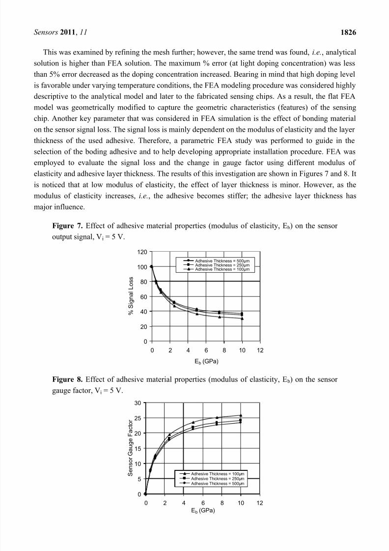
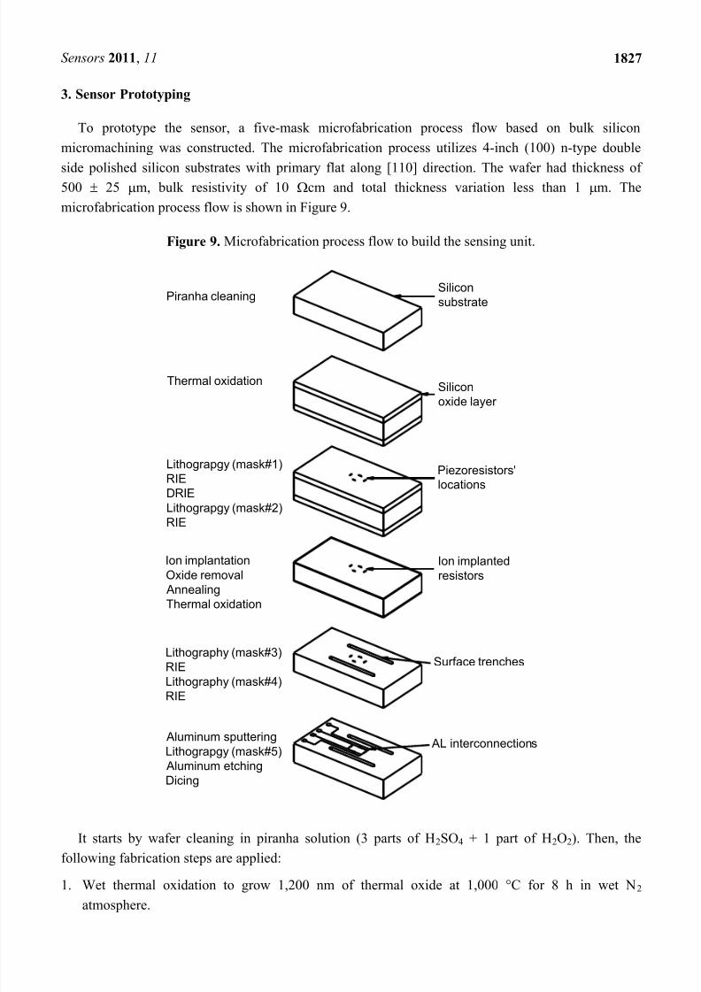
elasticity and adhesive layer thickness. The results of this investigation are shown in Figures 7 and 8. It
is noticed that at low modulus of elasticity, the effect of layer thickness is minor. However, as the
modulus of elasticity increases, i.e., the adhesive becomes stiffer; the adhesive layer thickness has
major influence.
Figure 7. Effect of adhesive material properties (modulus of elasticity, E b) on the sensor
output signal, Vi = 5 V.
0
20
40
60
80
100
120
0 2 4 6 8 10 12
Eb (GPa)
% S
i g n a l L
o s s
Adhesive Thickness = 500µm Adhesive Thickness = 250µm Adhesive Thickness = 100µm
Figure 8. Effect of adhesive material properties (modulus of elasticity, E b) on the sensor
gauge factor, Vi = 5 V.
0
5
10
15
20
25
30
0 2 4 6 8 10 12
Eb (GPa)
S e n s o r G a u g e F a c t o r
Adhesive Thickness = 100µm Adhesive Thickness = 250µm
Adhesive Thickness = 500µm
8/18/2019 Piezoresistive sensors-11-01819
http://slidepdf.com/reader/full/piezoresistive-sensors-11-01819 9/28
Sensors 2011, 11 1827
3. Sensor Prototyping
To prototype the sensor, a five-mask microfabrication process flow based on bulk silicon
micromachining was constructed. The microfabrication process utilizes 4-inch (100) n-type double
side polished silicon substrates with primary flat along [110] direction. The wafer had thickness of500 25 m, bulk resistivity of 10 cm and total thickness variation less than 1 m. The
microfabrication process flow is shown in Figure 9.
Figure 9. Microfabrication process flow to build the sensing unit.
Lithography (mask#3)
RIE
Lithography (mask#4)
RIE
Ion implantation
Oxide removal
Annealing
Thermal oxidation
Aluminum sputtering
Lithograpgy (mask#5)
Aluminum etching
Dicing
Lithograpgy (mask#1)
RIE
DRIE
Lithograpgy (mask#2)
RIE
Thermal oxidation
Piranha cleaning
AL interconnections
Surface trenches
Ion implanted
resistors
Piezoresistors'
locations
Silicon
oxide layer
Silicon
substrate
It starts by wafer cleaning in piranha solution (3 parts of H2SO4 + 1 part of H2O2). Then, the
following fabrication steps are applied:
1. Wet thermal oxidation to grow 1,200 nm of thermal oxide at 1,000 °C for 8 h in wet N2
atmosphere.
8/18/2019 Piezoresistive sensors-11-01819
http://slidepdf.com/reader/full/piezoresistive-sensors-11-01819 10/28
Sensors 2011, 11 1828
2. Lithography to pattern the first mask (alignment marks).
3. Reactive Ion Etching (RIE) then Deep Reactive Ion Etching (DRIE) to pattern the first mask in the
silicon substrate.
4. Lithography to define the piezoresistors’ locations using the second mask (doping windows).
5.
Boron ion-implantation with different doses (5.20 1012
, 5.20 1013
, 5.20 1014
, 5.20 1015
and5.20 1016 atoms/cm2) at energy level of 100 keV to create the p-type piezoresistive elements.
6.
Masking oxide layer removal using RIE.
7. Annealing at 1,100 °C for 15 minutes.
8. Wet thermal oxidation to grow an insulating oxide layer for one hour at 1,000 °C.
9. Lithography to pattern the contact via for the aluminum contacts using the third mask (contact via
openings).
10.
RIE to open contact via.
11.
Lithography to pattern the surface trenches using the fourth mask (surface trenches).
12.
RIE to remove oxide from backside of the silicon substrate.
13. DRIE to reduce the silicon wafer thickness.
14. Aluminum sputtering for 30 minutes to get aluminum layer of thickness 500 nm.
15. Lithography to define metallization traces and interconnects using the fifth mask (metallization and
interconnections).
16. Aluminum etching.
17.
Annealing at 450 °C for 20 minutes in dry N2 atmosphere.
18. Wafer dicing, preparation for wire bonding and testing.
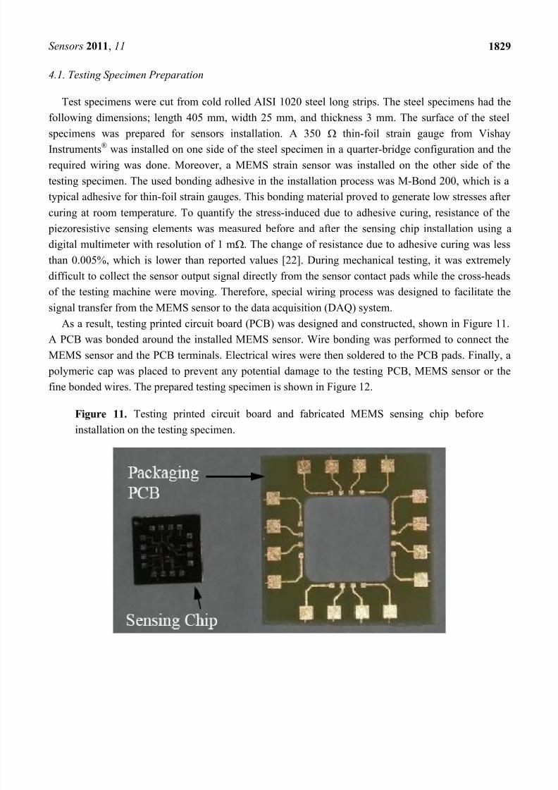
4. Experimental Setup and Testing Procedure
The fabricated sensing chip is shown in Figure 10. The experimental evaluation of the sensing chip
involved construction of the I-V characteristic curve in addition to the evaluation of thermal properties
(sensor TCRs), piezoresistive coefficient and stress/strain sensitivity. The following sections present
the procedure to carry out the experimental evaluation of the fabricated sensing chips.
Figure 10. Fabricated sensing chip.
8/18/2019 Piezoresistive sensors-11-01819
http://slidepdf.com/reader/full/piezoresistive-sensors-11-01819 11/28
Sensors 2011, 11 1829
4.1. Testing Specimen Preparation
Test specimens were cut from cold rolled AISI 1020 steel long strips. The steel specimens had the
following dimensions; length 405 mm, width 25 mm, and thickness 3 mm. The surface of the steel
specimens was prepared for sensors installation. A 350 thin-foil strain gauge from VishayInstruments® was installed on one side of the steel specimen in a quarter-bridge configuration and the
required wiring was done. Moreover, a MEMS strain sensor was installed on the other side of the
testing specimen. The used bonding adhesive in the installation process was M-Bond 200, which is a
typical adhesive for thin-foil strain gauges. This bonding material proved to generate low stresses after
curing at room temperature. To quantify the stress-induced due to adhesive curing, resistance of the
piezoresistive sensing elements was measured before and after the sensing chip installation using a
digital multimeter with resolution of 1 m. The change of resistance due to adhesive curing was less
than 0.005%, which is lower than reported values [22]. During mechanical testing, it was extremely
difficult to collect the sensor output signal directly from the sensor contact pads while the cross-headsof the testing machine were moving. Therefore, special wiring process was designed to facilitate the
signal transfer from the MEMS sensor to the data acquisition (DAQ) system.
As a result, testing printed circuit board (PCB) was designed and constructed, shown in Figure 11.
A PCB was bonded around the installed MEMS sensor. Wire bonding was performed to connect the
MEMS sensor and the PCB terminals. Electrical wires were then soldered to the PCB pads. Finally, a
polymeric cap was placed to prevent any potential damage to the testing PCB, MEMS sensor or the
fine bonded wires. The prepared testing specimen is shown in Figure 12.
Figure 11. Testing printed circuit board and fabricated MEMS sensing chip beforeinstallation on the testing specimen.
8/18/2019 Piezoresistive sensors-11-01819
http://slidepdf.com/reader/full/piezoresistive-sensors-11-01819 12/28
Sensors 2011, 11 1830
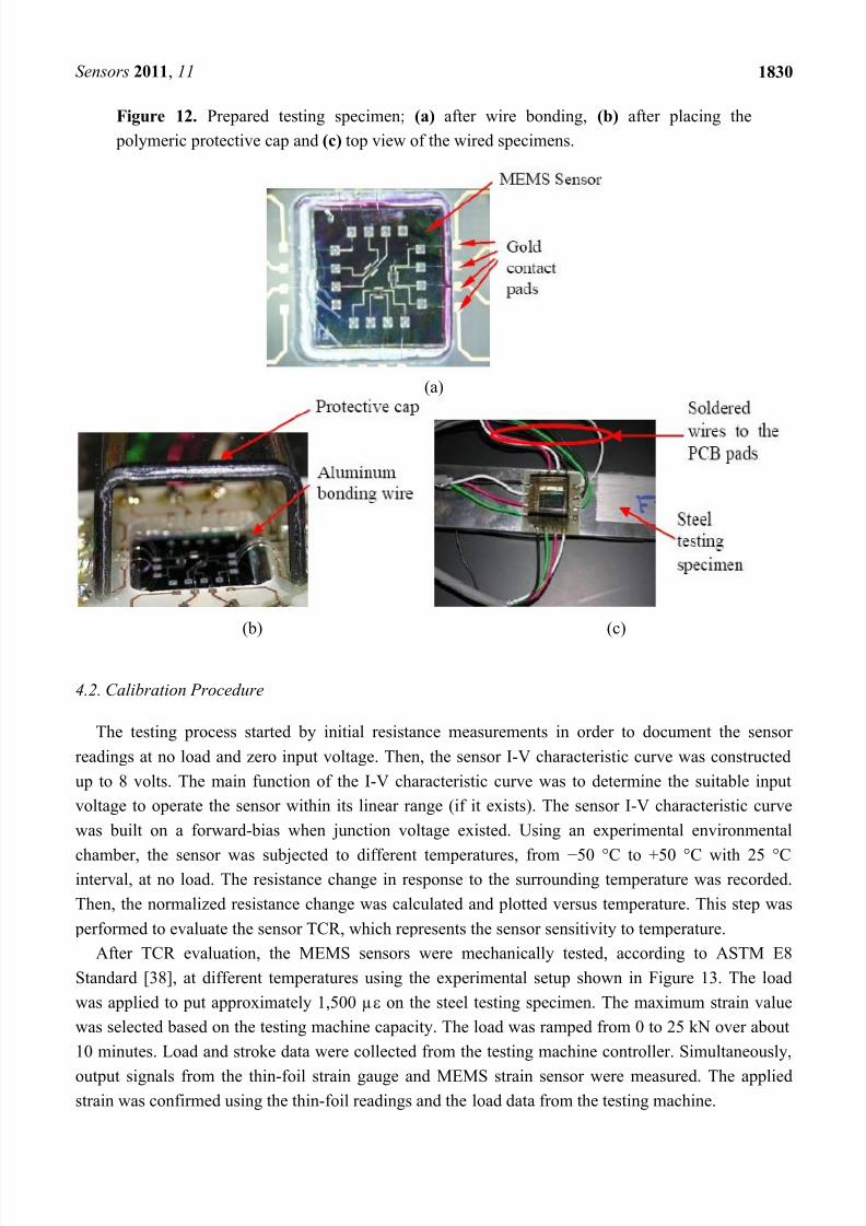
Figure 12. Prepared testing specimen; (a) after wire bonding, (b) after placing the
polymeric protective cap and (c) top view of the wired specimens.
(a)
(b) (c)
4.2. Calibration Procedure
The testing process started by initial resistance measurements in order to document the sensor
readings at no load and zero input voltage. Then, the sensor I-V characteristic curve was constructed
up to 8 volts. The main function of the I-V characteristic curve was to determine the suitable input
voltage to operate the sensor within its linear range (if it exists). The sensor I-V characteristic curve
was built on a forward-bias when junction voltage existed. Using an experimental environmental
chamber, the sensor was subjected to different temperatures, from −50 °C to +50 °C with 25 °Cinterval, at no load. The resistance change in response to the surrounding temperature was recorded.
Then, the normalized resistance change was calculated and plotted versus temperature. This step was
performed to evaluate the sensor TCR, which represents the sensor sensitivity to temperature.
After TCR evaluation, the MEMS sensors were mechanically tested, according to ASTM E8
Standard [38], at different temperatures using the experimental setup shown in Figure 13. The load
was applied to put approximately 1,500 µ on the steel testing specimen. The maximum strain value
was selected based on the testing machine capacity. The load was ramped from 0 to 25 kN over about
10 minutes. Load and stroke data were collected from the testing machine controller. Simultaneously,
output signals from the thin-foil strain gauge and MEMS strain sensor were measured. The applied
strain was confirmed using the thin-foil readings and the load data from the testing machine.
8/18/2019 Piezoresistive sensors-11-01819
http://slidepdf.com/reader/full/piezoresistive-sensors-11-01819 13/28
Sensors 2011, 11 1831
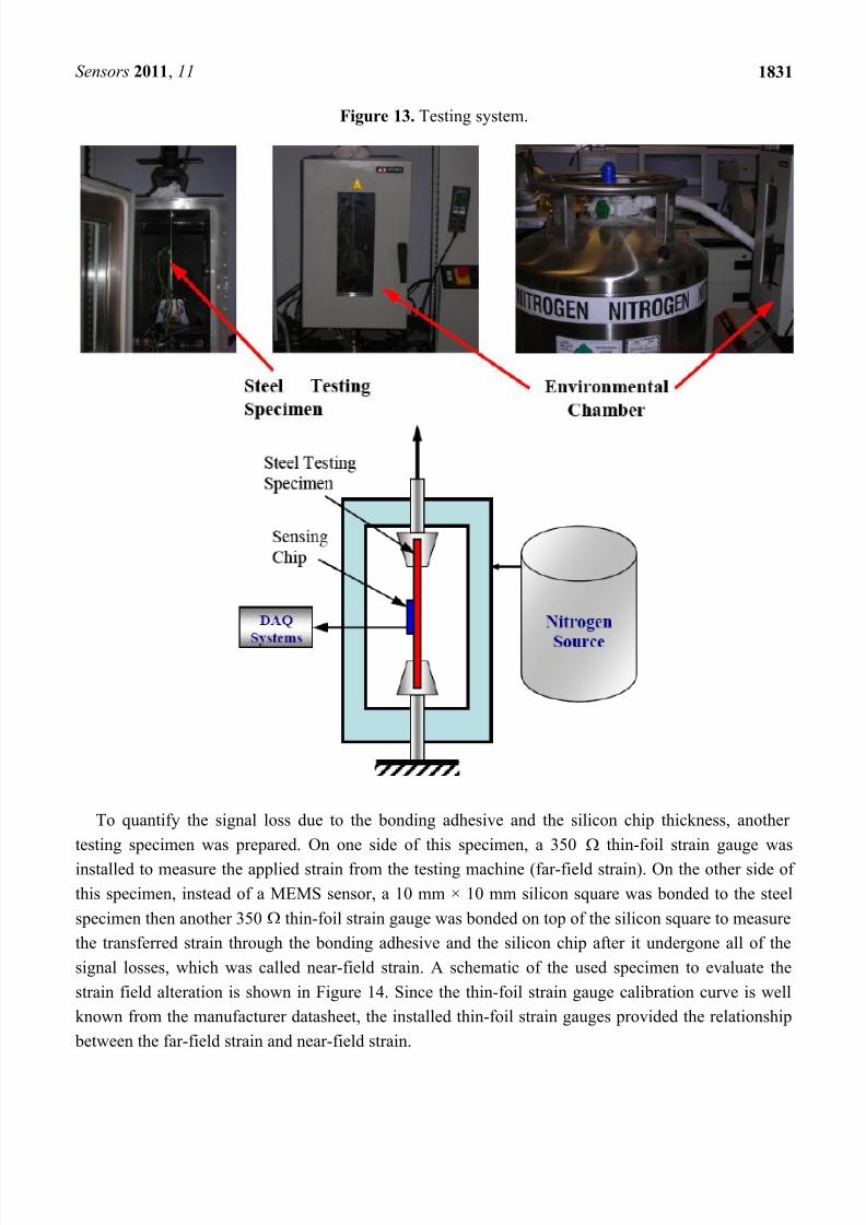
Figure 13. Testing system.
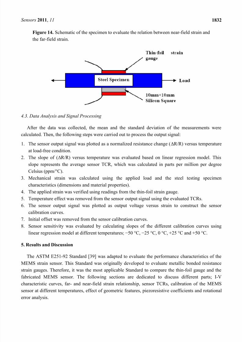
To quantify the signal loss due to the bonding adhesive and the silicon chip thickness, another
testing specimen was prepared. On one side of this specimen, a 350 thin-foil strain gauge was
installed to measure the applied strain from the testing machine (far-field strain). On the other side of
this specimen, instead of a MEMS sensor, a 10 mm × 10 mm silicon square was bonded to the steel
specimen then another 350 thin-foil strain gauge was bonded on top of the silicon square to measure
the transferred strain through the bonding adhesive and the silicon chip after it undergone all of the
signal losses, which was called near-field strain. A schematic of the used specimen to evaluate the
strain field alteration is shown in Figure 14. Since the thin-foil strain gauge calibration curve is well
known from the manufacturer datasheet, the installed thin-foil strain gauges provided the relationship
between the far-field strain and near-field strain.
8/18/2019 Piezoresistive sensors-11-01819
http://slidepdf.com/reader/full/piezoresistive-sensors-11-01819 14/28
Sensors 2011, 11 1832
Figure 14. Schematic of the specimen to evaluate the relation between near-field strain and
the far-field strain.
4.3. Data Analysis and Signal Processing
After the data was collected, the mean and the standard deviation of the measurements were
calculated. Then, the following steps were carried out to process the output signal:
1. The sensor output signal was plotted as a normalized resistance change (R/R) versus temperature
at load-free condition.
2. The slope of (R/R) versus temperature was evaluated based on linear regression model. This
slope represents the average sensor TCR, which was calculated in parts per million per degree
Celsius (ppm/°C).
3.
Mechanical strain was calculated using the applied load and the steel testing specimencharacteristics (dimensions and material properties).
4. The applied strain was verified using readings from the thin-foil strain gauge.
5. Temperature effect was removed from the sensor output signal using the evaluated TCRs.
6. The sensor output signal was plotted as output voltage versus strain to construct the sensor
calibration curves.
7. Initial offset was removed from the sensor calibration curves.
8. Sensor sensitivity was evaluated by calculating slopes of the different calibration curves using
linear regression model at different temperatures; −50 °C, −25 °C, 0 °C, +25 °C and +50 °C.
5. Results and Discussion
The ASTM E251-92 Standard [39] was adapted to evaluate the performance characteristics of the
MEMS strain sensor. This Standard was originally developed to evaluate metallic bonded resistance
strain gauges. Therefore, it was the most applicable Standard to compare the thin-foil gauge and the
fabricated MEMS sensor. The following sections are dedicated to discuss different parts; I-V
characteristic curves, far- and near-field strain relationship, sensor TCRs, calibration of the MEMS
sensor at different temperatures, effect of geometric features, piezoresistive coefficients and rotational
error analysis.
8/18/2019 Piezoresistive sensors-11-01819
http://slidepdf.com/reader/full/piezoresistive-sensors-11-01819 15/28
Sensors 2011, 11 1833
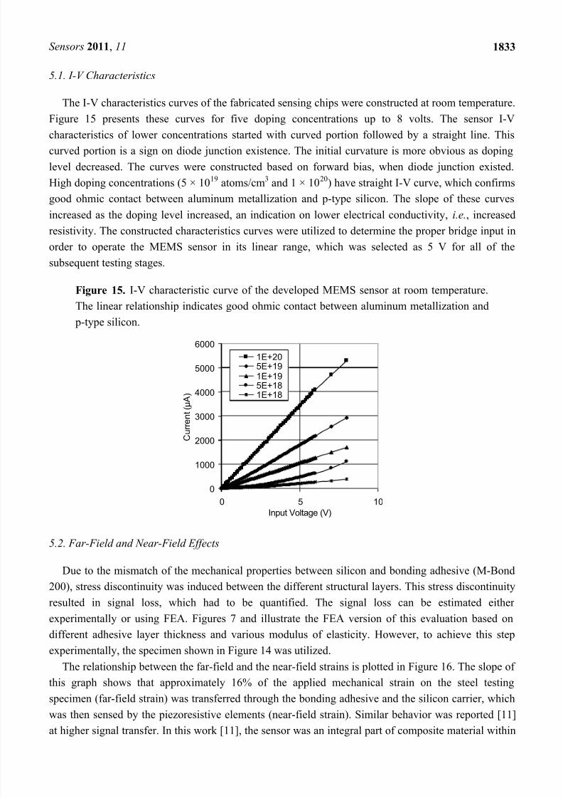
5.1. I-V Characteristics
The I-V characteristics curves of the fabricated sensing chips were constructed at room temperature.
Figure 15 presents these curves for five doping concentrations up to 8 volts. The sensor I-V
characteristics of lower concentrations started with curved portion followed by a straight line. Thiscurved portion is a sign on diode junction existence. The initial curvature is more obvious as doping
level decreased. The curves were constructed based on forward bias, when diode junction existed.
High doping concentrations (5 × 10¹⁹ atoms/cm3 and 1 × 10²⁰) have straight I-V curve, which confirms
good ohmic contact between aluminum metallization and p-type silicon. The slope of these curves
increased as the doping level increased, an indication on lower electrical conductivity, i.e., increased
resistivity. The constructed characteristics curves were utilized to determine the proper bridge input in
order to operate the MEMS sensor in its linear range, which was selected as 5 V for all of the
subsequent testing stages.
Figure 15. I-V characteristic curve of the developed MEMS sensor at room temperature.
The linear relationship indicates good ohmic contact between aluminum metallization and
p-type silicon.
0
1000
2000
3000
4000
5000
6000
0 5 10
Input Voltage (V)
C u r r e n t ( µ A )
1E+205E+191E+195E+181E+18
5.2. Far-Field and Near-Field Effects
Due to the mismatch of the mechanical properties between silicon and bonding adhesive (M-Bond
200), stress discontinuity was induced between the different structural layers. This stress discontinuity
resulted in signal loss, which had to be quantified. The signal loss can be estimated either
experimentally or using FEA. Figures 7 and illustrate the FEA version of this evaluation based on
different adhesive layer thickness and various modulus of elasticity. However, to achieve this step
experimentally, the specimen shown in Figure 14 was utilized.
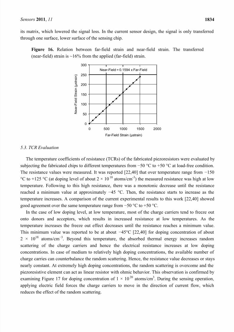
The relationship between the far-field and the near-field strains is plotted in Figure 16. The slope of
this graph shows that approximately 16% of the applied mechanical strain on the steel testing
specimen (far-field strain) was transferred through the bonding adhesive and the silicon carrier, whichwas then sensed by the piezoresistive elements (near-field strain). Similar behavior was reported [11]
at higher signal transfer. In this work [11], the sensor was an integral part of composite material within
8/18/2019 Piezoresistive sensors-11-01819
http://slidepdf.com/reader/full/piezoresistive-sensors-11-01819 16/28
Sensors 2011, 11 1834
its matrix, which lowered the signal loss. In the current sensor design, the signal is only transferred
through one surface, lower surface of the sensing chip.
Figure 16. Relation between far-field strain and near-field strain. The transferred
(near-field) strain is ~16% from the applied (far-field) strain.
Near-Field = 0.1594 x Far-Field
0
50
100
150
200
250
300
0 500 1000 1500 2000
Far-Field Strain (µstrain)
N e a r - F i e l d S t r a i n ( µ s t r a i n )
5.3. TCR Evaluation
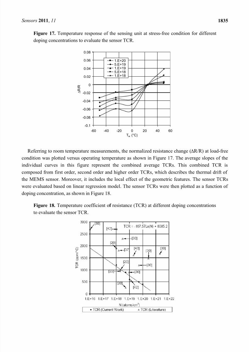
The temperature coefficients of resistance (TCRs) of the fabricated piezoresistors were evaluated by
subjecting the fabricated chips to different temperatures from −50 °C to +50 °C at load-free condition.
The resistance values were measured. It was reported [22,40] that over temperature range from −150°C to +125 °C (at doping level of about 2 × 10¹⁸ atoms/cm-3) the measured resistance was high at low
temperature. Following to this high resistance, there was a monotonic decrease until the resistance
reached a minimum value at approximately −45 °C. Then, the resistance starts to increase as the
temperature increases. A comparison of the current experimental results to this work [22,40] showed
good agreement over the same temperature range from −50 °C to +50 °C.
In the case of low doping level, at low temperature, most of the charge carriers tend to freeze out
onto donors and acceptors, which results in increased resistance at low temperatures. As the
temperature increases the freeze out effect decreases until the resistance reaches a minimum value.
This minimum value was reported to be at about −45°C [22,40] for doping concentration of about2 × 1018 atoms/cm−3. Beyond this temperature, the absorbed thermal energy increases random
scattering of the charge carriers and hence the electrical resistance increases at low doping
concentrations. In case of medium to relatively high doping concentrations, the available number of
charge carries can counterbalance the random scattering. Hence, the resistance value decreases or stays
nearly constant. At extremely high doping concentrations, the random scattering is overcome and the
piezoresistive element can act as linear resistor with ohmic behavior. This observation is confirmed by
examining Figure 17 for doping concentration of 1 × 10²⁰ atoms/cm3. During the sensing operation,
applying electric field forces the charge carriers to move in the direction of current flow, which
reduces the effect of the random scattering.
8/18/2019 Piezoresistive sensors-11-01819
http://slidepdf.com/reader/full/piezoresistive-sensors-11-01819 17/28
Sensors 2011, 11 1835
Figure 17. Temperature response of the sensing unit at stress-free condition for different
doping concentrations to evaluate the sensor TCR.
-0.1
-0.08
-0.06
-0.04
-0.02
0
0.02
0.04
0.06
0.08
-60 -40 -20 0 20 40 60
Tw (°C)
R / R
1.E+205.E+191.E+195.E+181.E+18
Referring to room temperature measurements, the normalized resistance change (R/R) at load-free
condition was plotted versus operating temperature as shown in Figure 17. The average slopes of the
individual curves in this figure represent the combined average TCRs. This combined TCR is
composed from first order, second order and higher order TCRs, which describes the thermal drift of
the MEMS sensor. Moreover, it includes the local effect of the geometric features. The sensor TCRs
were evaluated based on linear regression model. The sensor TCRs were then plotted as a function of
doping concentration, as shown in Figure 18.
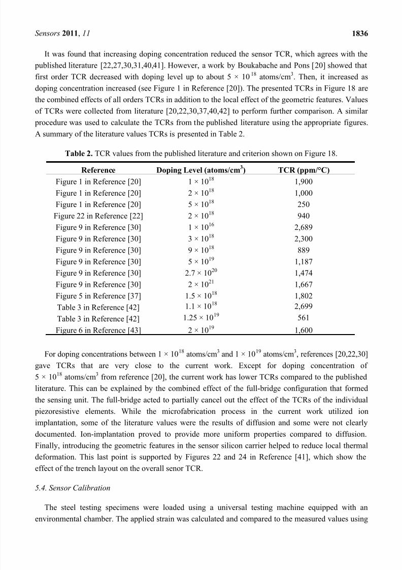
Figure 18. Temperature coefficient of resistance (TCR) at different doping concentrations
to evaluate the sensor TCR.
8/18/2019 Piezoresistive sensors-11-01819
http://slidepdf.com/reader/full/piezoresistive-sensors-11-01819 18/28
Sensors 2011, 11 1836
It was found that increasing doping concentration reduced the sensor TCR, which agrees with the
published literature [22,27,30,31,40,41]. However, a work by Boukabache and Pons [20] showed that
first order TCR decreased with doping level up to about 5 × 10 18 atoms/cm3. Then, it increased as
doping concentration increased (see Figure 1 in Reference [20]). The presented TCRs in Figure 18 are
the combined effects of all orders TCRs in addition to the local effect of the geometric features. Valuesof TCRs were collected from literature [20,22,30,37,40,42] to perform further comparison. A similar
procedure was used to calculate the TCRs from the published literature using the appropriate figures.
A summary of the literature values TCRs is presented in Table 2.
Table 2. TCR values from the published literature and criterion shown on Figure 18.
Reference Doping Level (atoms/cm3) TCR (ppm/°C)
Figure 1 in Reference [20] 1 × 10¹⁸ 1,900
Figure 1 in Reference [20] 2 × 10¹⁸ 1,000
Figure 1 in Reference [20] 5 × 10¹⁸ 250
Figure 22 in Reference [22] 2 × 10¹⁸ 940
Figure 9 in Reference [30] 1 × 10¹⁶ 2,689
Figure 9 in Reference [30] 3 × 10¹⁸ 2,300
Figure 9 in Reference [30] 9 × 10¹⁸ 889
Figure 9 in Reference [30] 5 × 10¹⁹ 1,187
Figure 9 in Reference [30] 2.7 × 10²⁰ 1,474
Figure 9 in Reference [30] 2 × 10²¹ 1,667
Figure 5 in Reference [37] 1.5 × 10
18
1,802Table 3 in Reference [42] 1.1 × 10¹⁸ 2,699
Table 3 in Reference [42] 1.25 × 10¹⁹ 561
Figure 6 in Reference [43] 2 × 10¹⁹ 1,600
For doping concentrations between 1 × 10¹⁸ atoms/cm3 and 1 × 10¹⁹ atoms/cm3, references [20,22,30]
gave TCRs that are very close to the current work. Except for doping concentration of
5 × 10¹⁸ atoms/cm3 from reference [20], the current work has lower TCRs compared to the published
literature. This can be explained by the combined effect of the full-bridge configuration that formed
the sensing unit. The full-bridge acted to partially cancel out the effect of the TCRs of the individual piezoresistive elements. While the microfabrication process in the current work utilized ion
implantation, some of the literature values were the results of diffusion and some were not clearly
documented. Ion-implantation proved to provide more uniform properties compared to diffusion.
Finally, introducing the geometric features in the sensor silicon carrier helped to reduce local thermal
deformation. This last point is supported by Figures 22 and 24 in Reference [41], which show the
effect of the trench layout on the overall senor TCR.
5.4. Sensor Calibration
The steel testing specimens were loaded using a universal testing machine equipped with an
environmental chamber. The applied strain was calculated and compared to the measured values using
8/18/2019 Piezoresistive sensors-11-01819
http://slidepdf.com/reader/full/piezoresistive-sensors-11-01819 19/28
Sensors 2011, 11 1837
thin-foil strain gauge. To deal with the fluctuations in readings, a statistical approach was adapted to
calculate the average reading of the measurements. The sensor calibration curves were constructed
using the applied strain (far-field strain) versus sensor output signal. Using the far-field strain to
construct the calibration curves included the effect of bonding adhesive in measurements. Therefore,
the calculated gauge factor and sensitivity were called equivalent gauge factor and equivalentsensitivity, respectively. The relationships between the equivalent parameters (gauge factor and
sensitivity) and their corresponding piezoresistive values can be defined experimentally or through
FEA. Figure 7 and Figure 8 present the FEA results and Figure 18 establishes this relationship
experimentally.
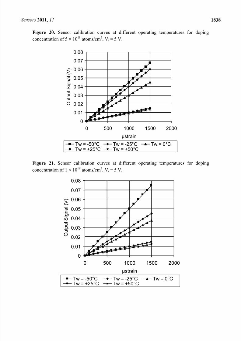
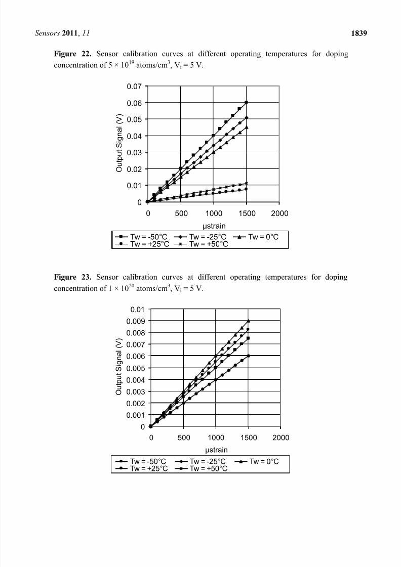
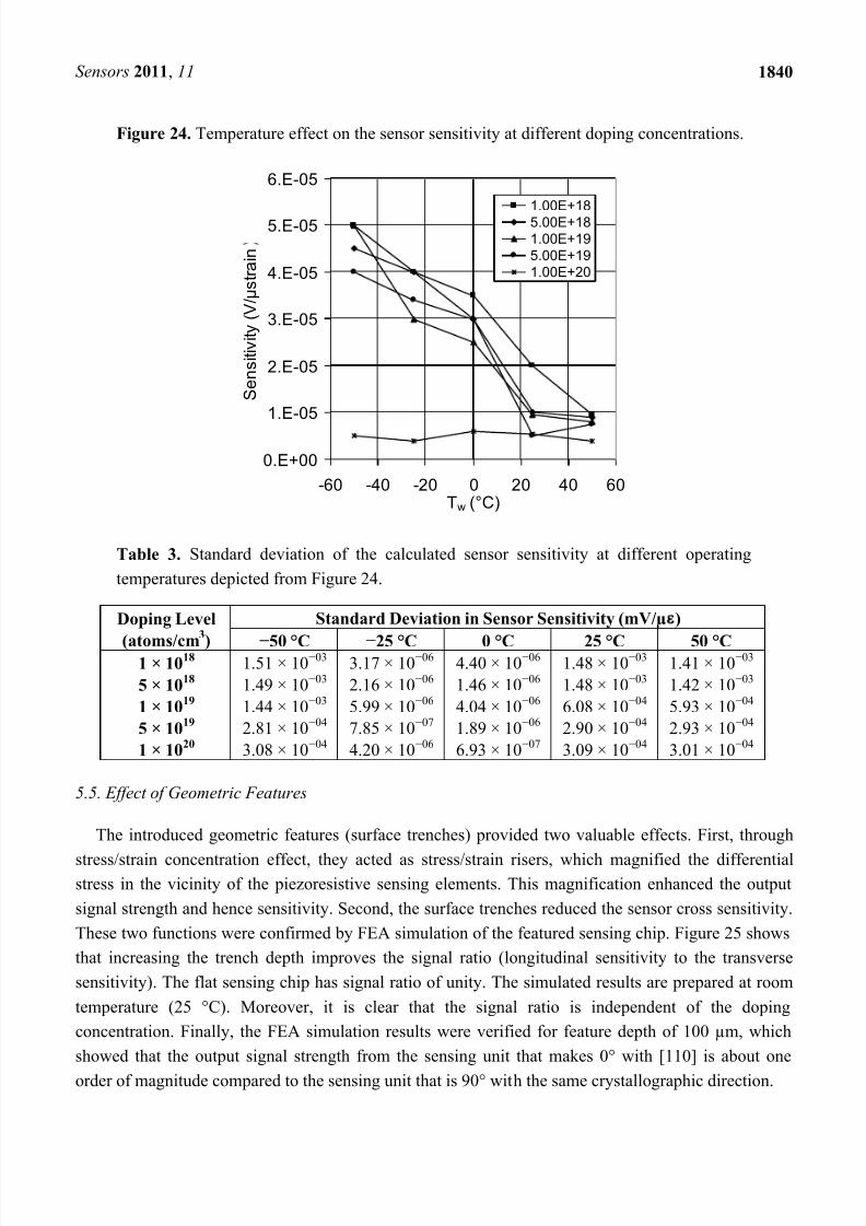
As discussed above, Figure 18 showed systematic decrease in the sensor TCR as the doping
concentration increases. For example, at doping concentration of 1 × 10²⁰ atoms/cm3, the TCR has
dropped to about one third of its value at doping concentration of 1 × 10¹⁸ atoms/cm3. This drop in the
sensor TCR helped to develop a MEMS piezoresistive sensor with low temperature drift; however, this
improvement in the sensor TCR came on the expense of the sensor equivalent sensitivity as shown in
Figures 19 through 23. As expected, the sensor output signal was found to follow linear relationship
with the applied mechanical strain/stress. The sensor calibration curves shown in Figure 19 through 23,
were constructed for various doping concentrations at different operating temperatures. Figure 24
summarizes the calibration results at different operating temperatures. Examining this figure
demonstrated that high doping concentration helped to stabilize the sensor output signal, which can be
depicted from the nearly horizontal line in Figure 24, which belongs to doping concentration of
1 × 10²⁰
atoms/cm3. On the other hand, at low doping concentrations, due to the diode junction, the
leakage current was temperature-dependent, which limits the capabilities of MEMS strain sensors
under varying temperature conditions. Values of standard deviation of the calculated sensor sensitivity
are listed in Table 3.
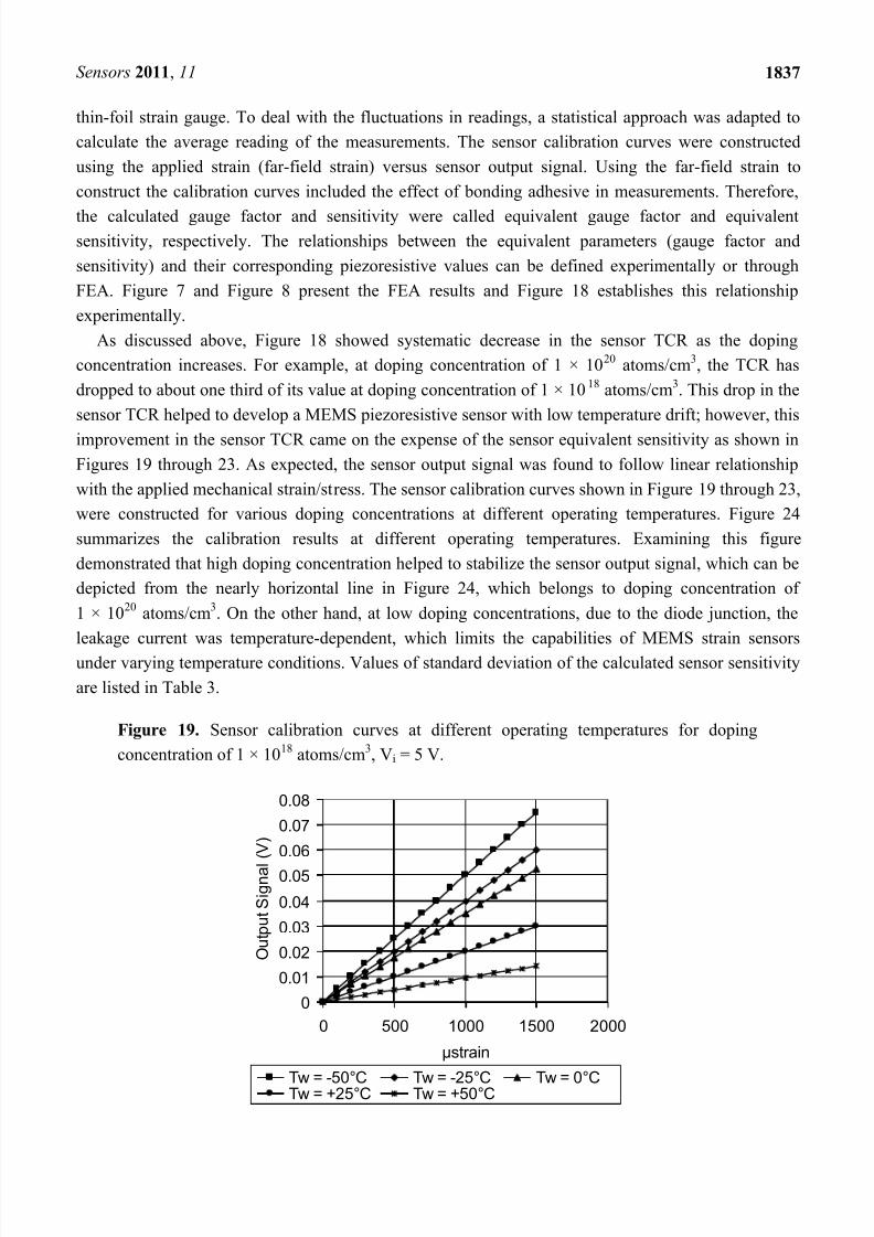
Figure 19. Sensor calibration curves at different operating temperatures for doping
concentration of 1 × 10¹⁸ atoms/cm3, Vi = 5 V.
0
0.01
0.02
0.03
0.04
0.05
0.06
0.07
0.08
0 500 1000 1500 2000
µstrain
O u t p u t S i g n a l ( V )
Tw = -50°C Tw = -25°C Tw = 0°CTw = +25°C Tw = +50°C
8/18/2019 Piezoresistive sensors-11-01819
http://slidepdf.com/reader/full/piezoresistive-sensors-11-01819 20/28
Sensors 2011, 11 1838
Figure 20. Sensor calibration curves at different operating temperatures for doping
concentration of 5 × 10¹⁸ atoms/cm3, Vi = 5 V.
0
0.01
0.02
0.03
0.04
0.05
0.06
0.07
0.08
0 500 1000 1500 2000
µstrain
O u t p u t S i g n a l ( V )
Tw = -50°C Tw = -25°C Tw = 0°CTw = +25°C Tw = +50°C
Figure 21. Sensor calibration curves at different operating temperatures for doping
concentration of 1 × 10¹⁹ atoms/cm3, Vi = 5 V.
0
0.010.02
0.03
0.04
0.05
0.06
0.07
0.08
0 500 1000 1500 2000
µstrain
O u t p u t S i g n a l ( V )
Tw = -50°C Tw = -25°C Tw = 0°CTw = +25°C Tw = +50°C
8/18/2019 Piezoresistive sensors-11-01819
http://slidepdf.com/reader/full/piezoresistive-sensors-11-01819 21/28
Sensors 2011, 11 1839
Figure 22. Sensor calibration curves at different operating temperatures for doping
concentration of 5 × 10¹⁹ atoms/cm3, Vi = 5 V.
0
0.01
0.02
0.03
0.04
0.05
0.06
0.07
0 500 1000 1500 2000
µstrain
O u t p u t S i g n a l ( V )
Tw = -50°C Tw = -25°C Tw = 0°CTw = +25°C Tw = +50°C
Figure 23. Sensor calibration curves at different operating temperatures for doping
concentration of 1 × 10²⁰ atoms/cm3, Vi = 5 V.
0
0.001
0.002
0.003
0.004
0.005
0.006
0.007
0.008
0.009
0.01
0 500 1000 1500 2000
µstrain
O u t p u t S i g n a l ( V )
Tw = -50°C Tw = -25°C Tw = 0°CTw = +25°C Tw = +50°C
8/18/2019 Piezoresistive sensors-11-01819
http://slidepdf.com/reader/full/piezoresistive-sensors-11-01819 22/28
Sensors 2011, 11 1840
Figure 24. Temperature effect on the sensor sensitivity at different doping concentrations.
0.E+00
1.E-05
2.E-05
3.E-05
4.E-05
5.E-05
6.E-05
-60 -40 -20 0 20 40 60Tw (°C)
S e n s i t i v i t y ( V / µ s t r a i n
1.00E+18
5.00E+18
1.00E+19
5.00E+19
1.00E+20
Table 3. Standard deviation of the calculated sensor sensitivity at different operating
temperatures depicted from Figure 24.
Doping Level
(atoms/cm3
)
Standard Deviation in Sensor Sensitivity (mV/µ
)
−50 °C
−25 °C 0 °C 25 °C 50 °C
1 × 10¹⁸
1.51 × 10−03 3.17 × 10−06 4.40 × 10−06 1.48 × 10−03 1.41 × 10−03
5 × 10¹⁸
1.49 × 10−03 2.16 × 10−06 1.46 × 10−06 1.48 × 10−03 1.42 × 10−03
1 × 10¹⁹
1.44 × 10−03 5.99 × 10−06 4.04 × 10−06 6.08 × 10−04 5.93 × 10−04
5 × 10¹⁹
2.81 × 10−04 7.85 × 10−07 1.89 × 10−06 2.90 × 10−04 2.93 × 10−04
1 × 10²⁰
3.08 × 10−04 4.20 × 10−06 6.93 × 10−07 3.09 × 10−04 3.01 × 10−04
5.5. Effect of Geometric Features
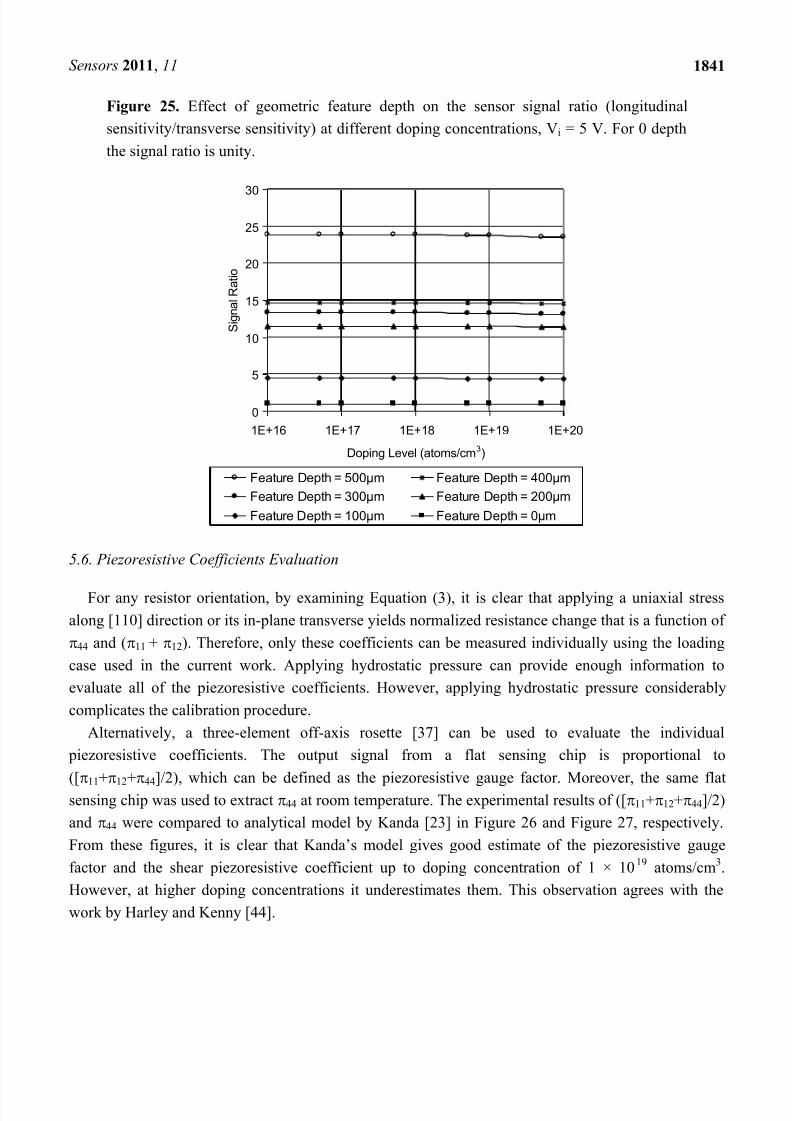
The introduced geometric features (surface trenches) provided two valuable effects. First, through
stress/strain concentration effect, they acted as stress/strain risers, which magnified the differentialstress in the vicinity of the piezoresistive sensing elements. This magnification enhanced the output
signal strength and hence sensitivity. Second, the surface trenches reduced the sensor cross sensitivity.
These two functions were confirmed by FEA simulation of the featured sensing chip. Figure 25 shows
that increasing the trench depth improves the signal ratio (longitudinal sensitivity to the transverse
sensitivity). The flat sensing chip has signal ratio of unity. The simulated results are prepared at room
temperature (25 °C). Moreover, it is clear that the signal ratio is independent of the doping
concentration. Finally, the FEA simulation results were verified for feature depth of 100 µm, which
showed that the output signal strength from the sensing unit that makes 0° with [110] is about one
order of magnitude compared to the sensing unit that is 90° with the same crystallographic direction.
8/18/2019 Piezoresistive sensors-11-01819
http://slidepdf.com/reader/full/piezoresistive-sensors-11-01819 23/28
Sensors 2011, 11 1841
Figure 25. Effect of geometric feature depth on the sensor signal ratio (longitudinal
sensitivity/transverse sensitivity) at different doping concentrations, V i = 5 V. For 0 depth
the signal ratio is unity.
0
5
10
15
20
25
30
1E+16 1E+17 1E+18 1E+19 1E+20
Doping Level (atoms/cm3)
S i g n a l R a t i o
Feature Depth = 500µm Feature Depth = 400µm
Feature Depth = 300µm Feature Depth = 200µm
Feature Depth = 100µm Feature Depth = 0µm
5.6. Piezoresistive Coefficients Evaluation
For any resistor orientation, by examining Equation (3), it is clear that applying a uniaxial stress
along [110] direction or its in-plane transverse yields normalized resistance change that is a function of
44 and (11 + 12). Therefore, only these coefficients can be measured individually using the loading
case used in the current work. Applying hydrostatic pressure can provide enough information to
evaluate all of the piezoresistive coefficients. However, applying hydrostatic pressure considerably
complicates the calibration procedure.
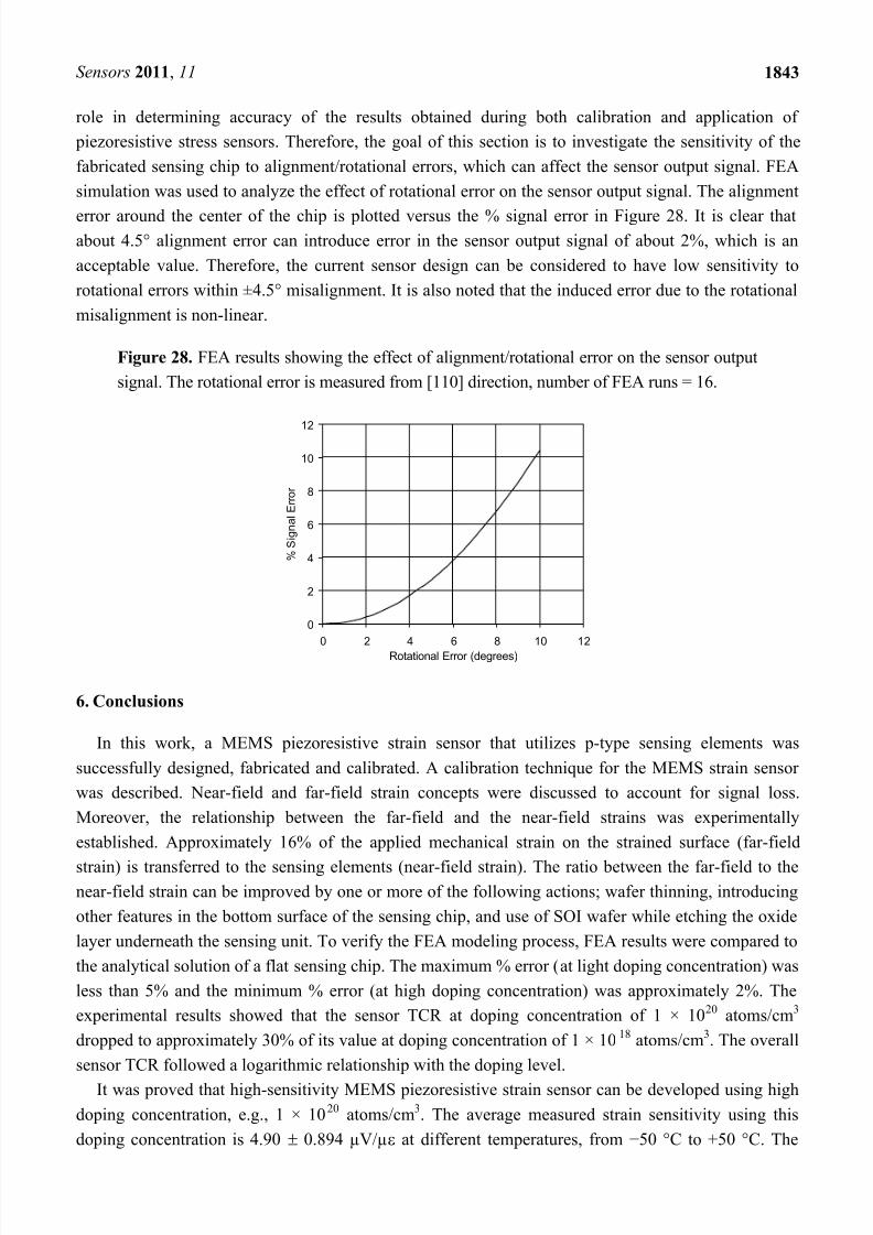
Alternatively, a three-element off-axis rosette [37] can be used to evaluate the individual
piezoresistive coefficients. The output signal from a flat sensing chip is proportional to
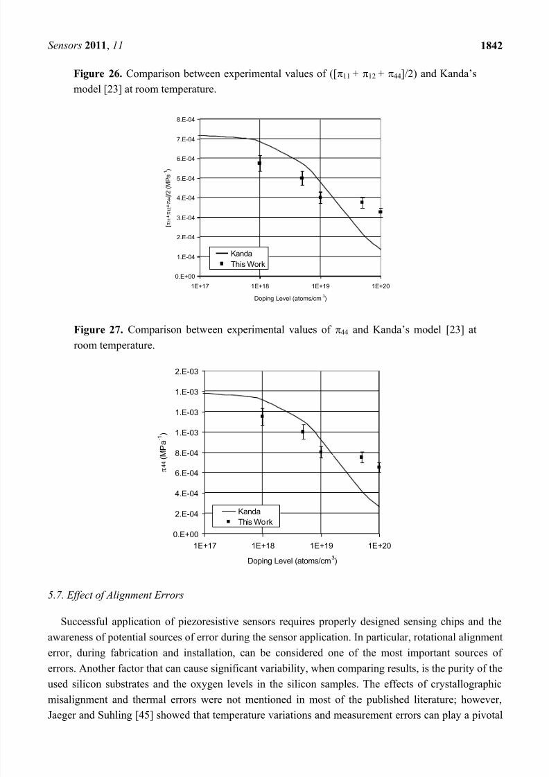
([11+12+44]/2), which can be defined as the piezoresistive gauge factor. Moreover, the same flatsensing chip was used to extract 44 at room temperature. The experimental results of ([11+12+44]/2)
and 44 were compared to analytical model by Kanda [23] in Figure 26 and Figure 27, respectively.
From these figures, it is clear that Kanda’s model gives good estimate of the piezoresistive gauge
factor and the shear piezoresistive coefficient up to doping concentration of 1 × 10 19 atoms/cm3.
However, at higher doping concentrations it underestimates them. This observation agrees with the
work by Harley and Kenny [44].
8/18/2019 Piezoresistive sensors-11-01819
http://slidepdf.com/reader/full/piezoresistive-sensors-11-01819 24/28
Sensors 2011, 11 1842
Figure 26. Comparison between experimental values of ([11 + 12 + 44]/2) and Kanda’s
model [23] at room temperature.
0.E+00
1.E-04
2.E-04
3.E-04
4.E-04
5.E-04
6.E-04
7.E-04
8.E-04
1E+17 1E+18 1E+19 1E+20
Doping Level (atoms/cm3)
[ 1 1 + 1 2 + 4 4 ] / 2 ( M P a - 1 )
Kanda
This Work
Figure 27. Comparison between experimental values of 44 and Kanda’s model [23] at
room temperature.
0.E+00
2.E-04
4.E-04
6.E-04
8.E-04
1.E-03
1.E-03
1.E-03
2.E-03
1E+17 1E+18 1E+19 1E+20
Doping Level (atoms/cm3)
4 4 ( M P a - 1 )
Kanda
This Work
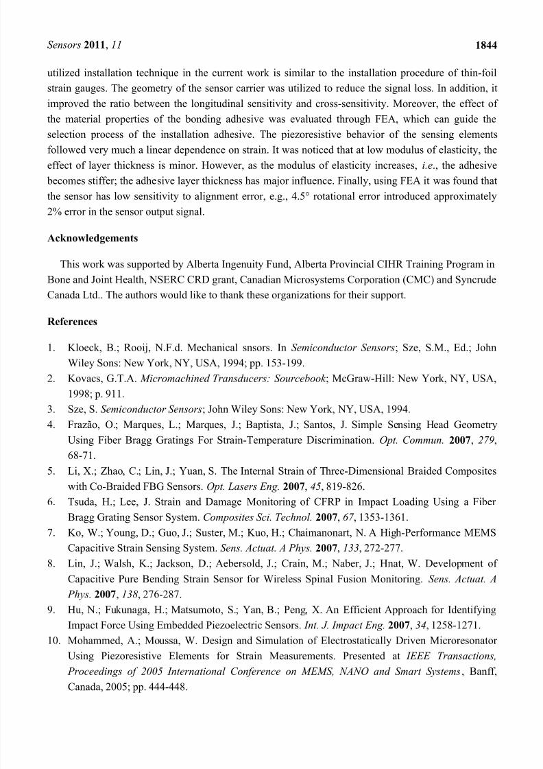
5.7. Effect of Alignment Errors
Successful application of piezoresistive sensors requires properly designed sensing chips and the
awareness of potential sources of error during the sensor application. In particular, rotational alignment
error, during fabrication and installation, can be considered one of the most important sources of
errors. Another factor that can cause significant variability, when comparing results, is the purity of the
used silicon substrates and the oxygen levels in the silicon samples. The effects of crystallographic
misalignment and thermal errors were not mentioned in most of the published literature; however,
Jaeger and Suhling [45] showed that temperature variations and measurement errors can play a pivotal
8/18/2019 Piezoresistive sensors-11-01819
http://slidepdf.com/reader/full/piezoresistive-sensors-11-01819 25/28
Sensors 2011, 11 1843
role in determining accuracy of the results obtained during both calibration and application of
piezoresistive stress sensors. Therefore, the goal of this section is to investigate the sensitivity of the
fabricated sensing chip to alignment/rotational errors, which can affect the sensor output signal. FEA
simulation was used to analyze the effect of rotational error on the sensor output signal. The alignment
error around the center of the chip is plotted versus the % signal error in Figure 28. It is clear thatabout 4.5° alignment error can introduce error in the sensor output signal of about 2%, which is an
acceptable value. Therefore, the current sensor design can be considered to have low sensitivity to
rotational errors within ±4.5° misalignment. It is also noted that the induced error due to the rotational
misalignment is non-linear.
Figure 28. FEA results showing the effect of alignment/rotational error on the sensor output
signal. The rotational error is measured from [110] direction, number of FEA runs = 16.
0
2
4
6
8
10
12
0 2 4 6 8 10 12
Rotational Error (degrees)
% S
i g n a l E r r o r
6. Conclusions
In this work, a MEMS piezoresistive strain sensor that utilizes p-type sensing elements was
successfully designed, fabricated and calibrated. A calibration technique for the MEMS strain sensor
was described. Near-field and far-field strain concepts were discussed to account for signal loss.
Moreover, the relationship between the far-field and the near-field strains was experimentally
established. Approximately 16% of the applied mechanical strain on the strained surface (far-field
strain) is transferred to the sensing elements (near-field strain). The ratio between the far-field to thenear-field strain can be improved by one or more of the following actions; wafer thinning, introducing
other features in the bottom surface of the sensing chip, and use of SOI wafer while etching the oxide
layer underneath the sensing unit. To verify the FEA modeling process, FEA results were compared to
the analytical solution of a flat sensing chip. The maximum % error (at light doping concentration) was
less than 5% and the minimum % error (at high doping concentration) was approximately 2%. The
experimental results showed that the sensor TCR at doping concentration of 1 × 10²⁰ atoms/cm3
dropped to approximately 30% of its value at doping concentration of 1 × 10¹⁸ atoms/cm3. The overall
sensor TCR followed a logarithmic relationship with the doping level.
It was proved that high-sensitivity MEMS piezoresistive strain sensor can be developed using high
doping concentration, e.g., 1 × 10²⁰ atoms/cm3. The average measured strain sensitivity using this
doping concentration is 4.90 0.894 µV/µ at different temperatures, from −50 °C to +50 °C. The
8/18/2019 Piezoresistive sensors-11-01819
http://slidepdf.com/reader/full/piezoresistive-sensors-11-01819 26/28
Sensors 2011, 11 1844
utilized installation technique in the current work is similar to the installation procedure of thin-foil
strain gauges. The geometry of the sensor carrier was utilized to reduce the signal loss. In addition, it
improved the ratio between the longitudinal sensitivity and cross-sensitivity. Moreover, the effect of
the material properties of the bonding adhesive was evaluated through FEA, which can guide the
selection process of the installation adhesive. The piezoresistive behavior of the sensing elementsfollowed very much a linear dependence on strain. It was noticed that at low modulus of elasticity, the
effect of layer thickness is minor. However, as the modulus of elasticity increases, i.e., the adhesive
becomes stiffer; the adhesive layer thickness has major influence. Finally, using FEA it was found that
the sensor has low sensitivity to alignment error, e.g., 4.5° rotational error introduced approximately
2% error in the sensor output signal.
Acknowledgements
This work was supported by Alberta Ingenuity Fund, Alberta Provincial CIHR Training Program inBone and Joint Health, NSERC CRD grant, Canadian Microsystems Corporation (CMC) and Syncrude
Canada Ltd.. The authors would like to thank these organizations for their support.
References
1. Kloeck, B.; Rooij, N.F.d. Mechanical snsors. In Semiconductor Sensors; Sze, S.M., Ed.; John
Wiley Sons: New York, NY, USA, 1994; pp. 153-199.
2. Kovacs, G.T.A. Micromachined Transducers: Sourcebook ; McGraw-Hill: New York, NY, USA,
1998; p. 911.
3. Sze, S. Semiconductor Sensors; John Wiley Sons: New York, NY, USA, 1994.
4. Frazão, O.; Marques, L.; Marques, J.; Baptista, J.; Santos, J. Simple Sensing Head Geometry
Using Fiber Bragg Gratings For Strain-Temperature Discrimination. Opt. Commun. 2007, 279,
68-71.
5. Li, X.; Zhao, C.; Lin, J.; Yuan, S. The Internal Strain of Three-Dimensional Braided Composites
with Co-Braided FBG Sensors. Opt. Lasers Eng. 2007, 45, 819-826.
6. Tsuda, H.; Lee, J. Strain and Damage Monitoring of CFRP in Impact Loading Using a Fiber
Bragg Grating Sensor System. Composites Sci. Technol. 2007, 67 , 1353-1361.
7. Ko, W.; Young, D.; Guo, J.; Suster, M.; Kuo, H.; Chaimanonart, N. A High-Performance MEMS
Capacitive Strain Sensing System. Sens. Actuat. A Phys. 2007, 133, 272-277.
8. Lin, J.; Walsh, K.; Jackson, D.; Aebersold, J.; Crain, M.; Naber, J.; Hnat, W. Development of
Capacitive Pure Bending Strain Sensor for Wireless Spinal Fusion Monitoring. Sens. Actuat. A
Phys. 2007, 138, 276-287.
9. Hu, N.; Fukunaga, H.; Matsumoto, S.; Yan, B.; Peng, X. An Efficient Approach for Identifying
Impact Force Using Embedded Piezoelectric Sensors. Int. J. Impact Eng. 2007, 34, 1258-1271.
10. Mohammed, A.; Moussa, W. Design and Simulation of Electrostatically Driven Microresonator
Using Piezoresistive Elements for Strain Measurements. Presented at IEEE Transactions,
Proceedings of 2005 International Conference on MEMS, NANO and Smart Systems, Banff,Canada, 2005; pp. 444-448.
8/18/2019 Piezoresistive sensors-11-01819
http://slidepdf.com/reader/full/piezoresistive-sensors-11-01819 27/28
Sensors 2011, 11 1845
11. Cao, L.; Kim, T.; Mantell, S.; Polla, D. Simulation and Fabrication of Piezoresistive Membrane
Type MEMS Strain Sensors. Sens. Actuat. A Phys. 2000, 80, 273-279.
12. Han, B.; Ou, J. Embedded Piezoresistive Cement-Based Stress/Strain Sensor. Sens. Actuat. A
Phys. 2007, 138, 294-298.
13. Mohammed, A.A.S.; Moussa, W.A.; Lou, E. Mechanical Strain Measurements UsingSemiconductor Piezoresistive Material. In Proceedings of 2006 International Conference on
MEMS, NANO and Smart Systems, ICMENS , Cairo, Egypt, December 27−29, 2006; pp. 5-6.
14. Mohammed, A.A.S.; Moussa, W.A.; Lou, E. High Sensitivity MEMS Strain Sensor: Design and
Simulation. Sensors 2008, 8, 2642-2661.
15. Mohammed, A.A.S.; Moussa, W.A.; Lou, E. Experimental Evaluation of a Novel Piezoresistive
MEMS Strain Sensor.2011, (In press).
16. Neumann, J.J.; Greve, D.W.; Oppenheim, I.J. Comparison of Piezoresistive and Capacitive
Ultrasonic Transducers. Presented at Smart Structures and Materials 2004 — Sensors and Smart
Structures Technologies for Civil, Mechanical, and Aerospace Systems, San Diego, CA, USA,
2004.
17. Kon, S.; Oldham, K.; Horowitz, R. Piezoresistive and Piezoelectric MEMS Strain Sensors for
Vibration Detection. Presented at Sensors and Smart Structures Technologies for Civil,
Mechanical, and Aerospace Systems 2007 , San Diego, CA, USA, 2007.
18. Rausch, J.; Heinickel, P.; Werthschuetzky, R.; Koegel, B.; Zogal, K.; Meissner, P. Experimental
Comparison of Piezoresistive MEMS and Fiber Bragg Grating Strain Sensors. Presented at IEEE
Sensors 2009 Conference — SENSORS 2009, Christchurch, New zealand, 2009
19. Adams, E.N. Elastoresistance in p-type Ge and Si. Phys. Rev. 1954, 96 , 803-804.
20. Boukabache, A.; Pons, P. Doping Effects on Thermal Behaviour of Silicon Resistor. Electron.
Lett. 2002, 38, 342-343.
21. Brooks, H. Electrical Properties of Germanium and Silicon; Academic Press: New York, NY,
USA, 1955.
22. Cho, C.H.; Jaeger, R.C.; Suhling, J.C. Characterization of the temperature dependence of the
piezoresistive coefficients of silicon from −150 °C to +125 °C. IEEE Sens. J. 2008, 8, 1455-1468.
23. Kanda, Y. A Graphical Representation of the Piezoresistance Coefficients in Silicon. IEEE Trans.
Electron. Dev. 1982, ED-29, 64-70.
24. Kanda, Y. Piezoresistance Effect of Silicon. Sens. Actuat. A Phys. 1991, 28, 83-91.25. Kerr, D.; Milnes, A. Piezoresistance of Diffused Layers in Cubic Semiconductors. J. Appl. Phys.
1963, 34, 727-731.
26. Kozlovskiy, S.; Boiko, I. First-order Piezoresistance Coefficients in Silicon Crystals. Sens. Actuat.
A Phys. 2006, 118, 33-43.
27. Morin, F.J.; Geballe, T.H.; Herring, C. Temperature Dependence of the Piezoresistance of
High-Purity Silicon and Germanium. Phys. Rev. 1957, 10, 525-539.
28. Smith, C.S. Piezoresistance Effect in Germanium and Silicon. Phys. Rev. 1954, 94, 42-49.
29. Smith, C.S. Macroscopic Symmetry and Properties of Crystals. Solid State Phys. 1958, 6 , 175-
249.30. Tufte, O.N.; Stelzer, E.L. Piezoresistive Properties of Silicon Diffused Layers. J. Appl. Phys.
1963, 34, 3322-3327.
8/18/2019 Piezoresistive sensors-11-01819
http://slidepdf.com/reader/full/piezoresistive-sensors-11-01819 28/28