Embed Size (px)
Citation preview
Performance Optimization of VLSI Interconnect Layout
Jason Cong, Lei He, Cheng-Kok Koh and Patrick H. Madden
Department of Computer Science
University of California, Los Angeles, CA 90095
Abstract
This paper presents a comprehensive survey of existing techniques for interconnect optimizationduring the VLSI physical design
process, with emphasis on recent studies on interconnect design and optimization for high-performance VLSI circuit design un-
der the deep submicron fabrication technologies. First, we present a number of interconnect delay models and driver/gate delay
models of various degrees of accuracy and efficiency which are most useful to guide the circuit design and interconnect opti-
mization process. Then, we classify the existing work on optimization of VLSI interconnect into the following three categories
and discuss the results in each category in detail: (i) topology optimization for high-performance interconnects, including the
algorithms for total wirelength minimization, critical pathlength minimization, and delay minimization; (ii) device and intercon-
nect sizing, including techniques for efficient driver, gate, and transistor sizing, optimal wiresizing, and simultaneous topology
construction, buffer insertion, buffer and wire sizing; (iii) high-performance clock routing, including abstract clock net topol-
ogy generation and embedding, planar clock routing, buffer and wire sizing for clock nets, non-tree clock routing, and clock
schedule optimization. For each method, we discuss its effectiveness, its advantages and limitations, as well as its computa-
tional efficiency. We group the related techniques according to either their optimization techniques or optimization objectives
so that the reader can easily compare the quality and efficiency of different solutions.
1
Contents
1 Introduction 4
2 Preliminaries 5
2.1 Interconnect Delay Models 6
2.2 Driver Delay Models 12
3 Topology Optimization for High Performance Interconnect 16
3.1 Topology Optimization for Total Wirelength Minimization 18
3.1.1 Minimum Spanning Trees 18
3.1.2 Conventional Steiner Tree Algorithms 18
3.2 Topology Optimization for Path Length Minimization 22
3.2.1 Tree Cost/Path Length Tradeoffs 22
3.2.2 Arboresences 24
3.2.3 Multiple Source Routing 26
3.3 Topology Optimization for Delay Minimization 28
4 Wire and Device Sizing 31
4.1 Device Sizing 31
4.1.1 Driver Sizing 32
4.1.2 Transistor and Gate Sizing 33
4.1.3 Buffer Insertion 37
4.2 Wiresizing Optimization 39
4.2.1 Wiresizing to Minimize Weighted Delay 39
4.2.2 Wiresizing to Minimize Maximum Delay or Achieve Target Delay 44
4.3 Simultaneous Device and Wire Sizing 47
4.3.1 Simultaneous Driver and Wire Sizing 47
4.3.2 Simultaneous Gate and Wire Sizing 48
4.3.3 Simultaneous Transistor and Wire Sizing 49
4.3.4 Simultaneous Buffer Insertion and Wire Sizing 50
4.4 Simultaneous Topology Construction and Sizing 51
4.4.1 Dynamic Wiresizing during Topology Construction 51
4.4.2 Simultaneous Tree Construction, Buffer Insertion and Wiresizing 52
5 High-Performance Clock Routing 53
5.1 Abstract Topology Generation 55
5.1.1 Top-Down Topology Generation 56
5.1.2 Bottom-Up Topology Generation 57
2
5.2 Embedding of Abstract Topology 59
5.2.1 Zero-Skew Embedding 59
5.2.2 Bounded-Skew Embedding 62
5.2.3 Topology Generation with Embedding 66
5.3 Planar Clock Routing 68
5.3.1 Max-Min Planar Clock Routing 69
5.3.2 Planar-DME Clock Routing 69
5.4 Buffer and Wire Sizing for Clock Nets 70
5.4.1 Wiresizing in Clock Routing 72
5.4.2 Buffer Insertion in Clock Routing 74
5.4.3 Buffer Insertion and Sizing in Clock Routing 78
5.4.4 Buffer Insertion and Wire Sizing in Clock Routing 79
5.5 Non-Tree Clock Routing 81
5.6 Clock Schedule Optimization 81
6 Conclusion and Future Work 84
3
1 Introduction
The driving force behind the rapid growth of the VLSI technology has been the constant reduction of the feature size of VLSI
devices (i.e. the minimum transistor size). The feature size decreased from about 2µm in 1985, to about 1µm in 1990, and to
0.35-0.5µm today (1996). The prediction is that it will be reduced to about 0.18µm in Year 2001 [SIA94]. Such continual minia-
turization of VLSI devices has strong impact on the VLSI technology in several ways. First, the device density on integrated
circuits grows quadratically with the rate of decrease in the feature size. As a result, the total number of transistors on a sin-
gle VLSI chip has increased from less than 500,000 in 1985 to over 10 million today. The prediction is that it will reach 64
million in Year 2001 [SIA94]. Second, the devices operate at a higher speed, and the interconnect delay becomes much more
significant. According to the simple scaling rule described in [Ba90], when the devices and interconnects are scaled down in all
three dimensions by a factor of S, the intrinsic gate delay is reduced by a factor of S, the delay of local interconnects (such as
connections between adjacent gates) remains the same, but the delay of global interconnects increases by a factor of S2. As a
result, the interconnect delay has become the dominating factor in determining system performance. In many systems designed
today, as much as 50% to 70% of clock cycle are consumed by interconnect delays. This percentage will continue to rise as the
feature size decreases further.
Not only do interconnects become more important, they also become much more difficult to model and optimize in the deep
submicron VLSI technology, as the distributed nature of the interconnects has to be considered. Roughly speaking, the intercon-
nect delay is determined by the driver/gate resistance, the interconnect and loading capacitance, and the interconnect resistance.
For the conventional technology with the feature size of 1µm or above, the interconnect resistance in most cases is negligible
compared to the driver resistance. So, the interconnect and loading gates can be modeled as a lumped loading capacitor. In this
case, the interconnect delay is determined by the driver resistance times the total loading capacitance. Therefore, conventional
optimization techniques focus on reducing the driver resistance using driver, gate, and transistor sizing, and minimizing the in-
terconnect capacitance by buffer insertion and minimum-length, minimum-width routing. For the deep submicron technology
which became available recently, the interconnect resistance is comparable to the driver resistance in many cases. As a result,
the interconnect has to be modeled as a distributed RC or RLC circuit. Techniques such as optimal wire sizing, optimal buffer
placement, and simultaneous driver, buffer, and wire sizing have become necessary and important.
This paper presents an up-to-date survey of the existing techniques for interconnect optimization during the VLSI layout
design process. Section 2 discusses interconnect delay models and gate delay models and introduces a set of concepts and nota-
tion to be used for the subsequent sections. Section 3 presents the techniques for interconnect topology optimization, where the
objective is to compute the best routing pattern for a net for interconnect delay minimization. It covers the algorithms based on
total wirelength minimization, pathlength minimization, and delay minimization. Section 4 presents the techniques for device
and interconnect sizing, which determines the best geometric dimensions of devices and interconnects for delay minimization.
It includes driver sizing, transistor sizing, buffer placement, wire sizing, and combinations of these techniques. Section 5 dis-
cusses techniques for high-performance clock routing, including clock tree topology generation and embedding, planar clock
routing, buffer and wire sizing for clock nets, non-tree clock routing, and clock schedule optimization. Section 6 concludes the
paper with suggestions of several directions for future research.
4
2 Preliminaries
VLSI design involves a number of steps, including high level design, logic design, and physical layout. Designs are generally
composed of a number of functional blocks or cells which must be interconnected. This paper addresses the interconnection
problems of these blocks or cells.
A net N is composed of a set of pinss0 s1 s2 sn which must be made electrically connected. s0 denotes the driver of
the net, which supplies a signal to the interconnect. In some cases, a net may have multiple drivers, each driving the interconnect
at a different time (such as in a signal bus). These nets are called multi-source nets. The remaining pins in a net are sinks, which
receive the signal from the driver.
The interconnection of a net consists of a set of wire segments (often in multiple routing layers) connecting all the pins in
the net. It can be represented by a graph, in which each edge denotes a wire segment and each vertex denotes a pin or joint of
two wire segments. Interconnections are generally rectilinear.
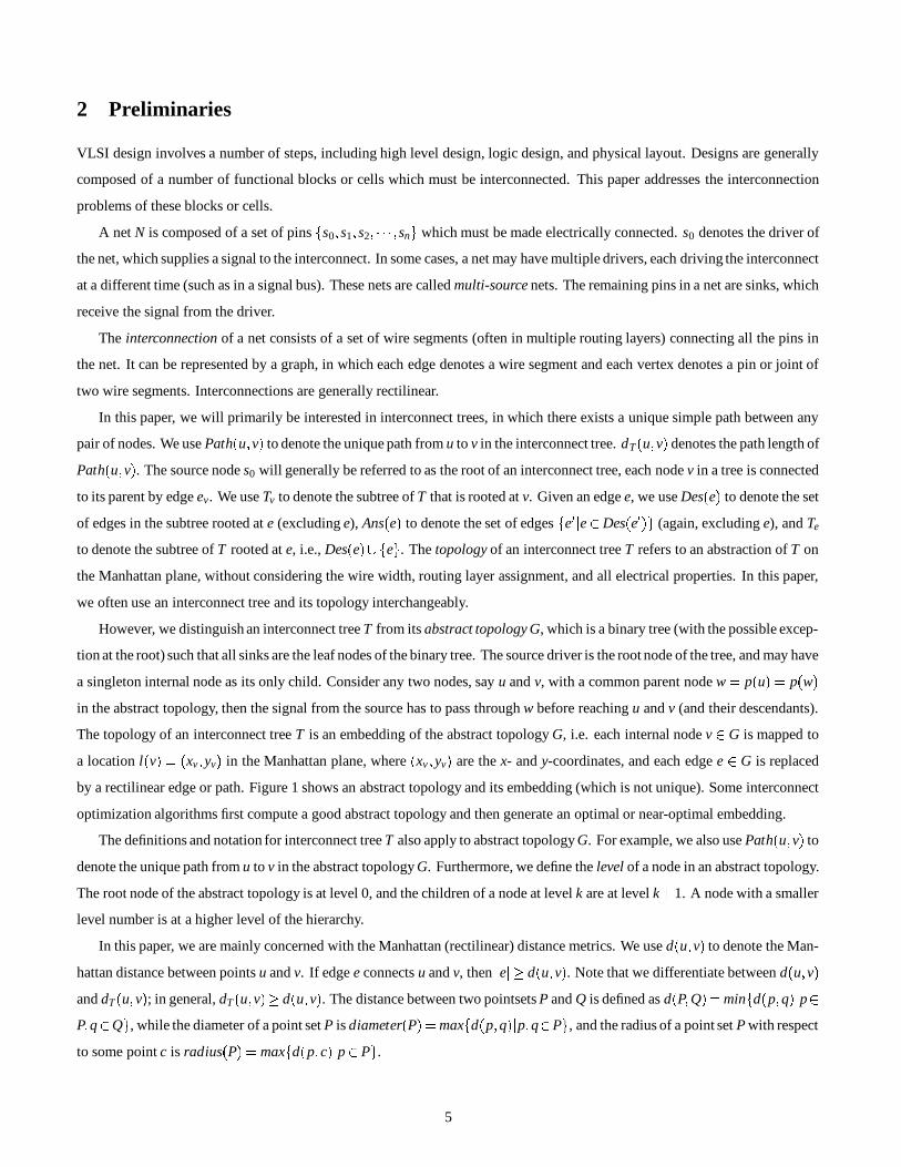
In this paper, we will primarily be interested in interconnect trees, in which there exists a unique simple path between any
pair of nodes. We use Path u v to denote the unique path from u to v in the interconnect tree. dT u v denotes the path length of
Path u v . The source node s0 will generally be referred to as the root of an interconnect tree, each node v in a tree is connected
to its parent by edge ev. We use Tv to denote the subtree of T that is rooted at v. Given an edge e, we use Des e to denote the set
of edges in the subtree rooted at e (excluding e), Ans e to denote the set of edgese e Des e (again, excluding e), and Te
to denote the subtree of T rooted at e, i.e., Des e e . The topology of an interconnect tree T refers to an abstraction of T on
the Manhattan plane, without considering the wire width, routing layer assignment, and all electrical properties. In this paper,
we often use an interconnect tree and its topology interchangeably.
However, we distinguish an interconnect tree T from its abstract topology G, which is a binary tree (with the possible excep-
tion at the root) such that all sinks are the leaf nodes of the binary tree. The source driver is the root node of the tree, and may have
a singleton internal node as its only child. Consider any two nodes, say u and v, with a common parent node w p u p w in the abstract topology, then the signal from the source has to pass through w before reaching u and v (and their descendants).
The topology of an interconnect tree T is an embedding of the abstract topology G, i.e. each internal node v G is mapped to
a location l v xv yv in the Manhattan plane, where xv yv are the x- and y-coordinates, and each edge e G is replaced
by a rectilinear edge or path. Figure 1 shows an abstract topology and its embedding (which is not unique). Some interconnect
optimization algorithms first compute a good abstract topology and then generate an optimal or near-optimal embedding.
The definitions and notation for interconnect tree T also apply to abstract topology G. For example, we also use Path u v to
denote the unique path from u to v in the abstract topology G. Furthermore, we define the level of a node in an abstract topology.
The root node of the abstract topology is at level 0, and the children of a node at level k are at level k 1. A node with a smaller
level number is at a higher level of the hierarchy.
In this paper, we are mainly concerned with the Manhattan (rectilinear) distance metrics. We use d u v to denote the Man-
hattan distance between points u and v. If edge e connects u and v, then e d u v . Note that we differentiate between d u v and dT u v ; in general, dT u v d u v . The distance between two pointsets P and Q is defined as d P Q min
d p q p
P q Q , while the diameter of a point set P is diameter P maxd p q p q P , and the radius of a point set P with respect
to some point c is radius P maxd p c p P .
5
s3
0s
1s
2s
0s
1s
2s s
3
u
v
Figure 1: The abstract topology of an interconnect tree, and its embedding.
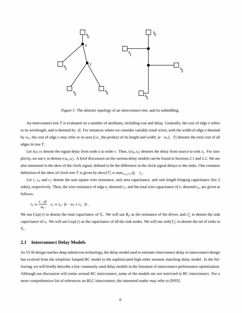
An interconnect tree T is evaluated on a number of attributes, including cost and delay. Generally, the cost of edge e refers
to its wirelength, and is denoted by e . For instances where we consider variably sized wires, with the width of edge e denoted
by we, the cost of edge e may refer to its area (i.e., the product of its length and width, e we). T denotes the total cost of all
edges in tree T .
Let t u v denote the signal delay from node u to node v. Then, t s0 si denotes the delay from source to sink si. For sim-
plicity, we use ti to denote t s0 si . A brief discussion on the various delay models can be found in Sections 2.1 and 2.2. We are
also interested in the skew of the clock signal, defined to be the difference in the clock signal delays to the sinks. One common
definition of the skew of clock tree T is given by skew T maxsi s j
S ti t j .Let r, ca and c f denote the unit square wire resistance, unit area capacitance, and unit length fringing capacitance (for 2
sides), respectively. Then, the wire resistance of edge e, denoted re, and the total wire capacitance of e, denoted ce, are given as
follows:
re r e we
ce ca e we c f e
We use Cap v to denote the total capacitance of Tv. We will use Rd as the resistance of the driver, and cssi
to denote the sink
capacitance of si. We will use Cap S as the capacitance of all the sink nodes. We will use sink Tv to denote the set of sinks in
Tv.
2.1 Interconnect Delay Models
As VLSI design reaches deep submicron technology, the delay model used to estimate interconnect delay in interconnect design
has evolved from the simplistic lumped RC model to the sophisticated high order moment matching delay model. In the fol-
lowing, we will briefly describe a few commonly used delay models in the literature of interconnect performance optimization.
Although our discussion will center around RC interconnect, some of the models are not restricted to RC interconnect. For a
more comprehensive list of references on RLC interconnect, the interested reader may refer to [Pi95].
6
In the lumped RC model, “R” refers to the resistance of the driver and “C” refers to the sum of the total capacitance of the
interconnect and the total gate capacitance of the sinks. The model assumes that wire resistance is negligible. This is generally
true for circuits with feature sizes of 1 2µm and above since the driver resistance is substantially larger than the total wire resis-
tance. In this case, the switching time of the gate dominates the time for the signal to travel along the interconnect and the sinks
are considered to receive the signal at the same time due to the negligible wire resistance.
However, as the feature size decreases to the submicron dimension, the wire resistance is no longer negligible. Sinks that are
farther from the source generally have a longer delay. For example, under the pathlength (or linear) delay model, the delay from
u to v in an interconnect tree is proportional to the sum of edgelengths in the unique u-v path, i.e., t u v ∝ ∑ew
Path u v ew . The
limitation of the pathlength delay model is that it ignores the wire resistance but consider only wire capacitance along the path.
Moreover, it ignores the effect of edges not along the path. The merit of the pathlength delay model is that routing problems for
pathlength control or optimization are generally much easier than delay optimization under more sophisticated delay models to
be presented below.
The delay models presented in the remainder of this section consider both wire resistance and capacitance of the interconnect.
Under these models, the interconnect is modeled as an RC tree, which is recursively defined as follows [RuPH83]: (i) a lumped
capacitor between ground and another node is an RC tree, (ii) a lumped resistor between two nonground nodes is an RC tree,
(iii) an RC line with no dc path to ground is an RC tree, and (iv) any two RC trees (with common ground) connected together
to a nonground node is an RC tree. We can extend the above definition for RLC tree easily by considering inductors and RLC
lines.
Given an RC tree, Rubinstein, Penfield, and Horowitz [RuPH83] compute a uniform upper bound of signal delay at every
node, denoted tP, as follows:
tP ∑all nodes k
Rkk Ck (1)
where Ck is the capacitance of the lumped capacitor at node k and Rki is defined to be the resistance of the portion of the (unique)
path Path s0 i that is common with the (unique) path Path s0 k . In particular, Rkk is the resistance between the source and
node k. There are a few advantages of this model: (i) it is simple, yet still captures the distributed nature of the circuit; (ii) it
gives a uniform delay upper bound and is easier to use for interconnect design optimization; (iii) it correlates reasonably well
with the Elmore delay model, which will be discussed next.
The Elmore delay model [El48] is the most commonly used delay model in recent works on interconnect design. Under the
Elmore delay model, the signal delay from source s0 to node i in an RC tree is given by [RuPH83]:
t s0 i ∑all nodes k
Rki Ck (2)
Unlike the upper bound signal delay model in Eqn. (1), each sink (and in fact, all nodes in the RC tree) has a separate delay
measure under the Elmore delay model. It is used to estimate the 50% delay of a monotonic step response (to a step input) by
the mean of the impulse response, which is given by ∞0 t h t dt where h t is the impulse response. The impulse response h t
can be viewed as either (i) the response to the unit impulse (applied at time 0) at time t, or (ii) the derivative of the unit step
response at time t. The 50% delay, denoted t50, is the time for the monotonic step response to reach 50% of VDD, and it is the
7
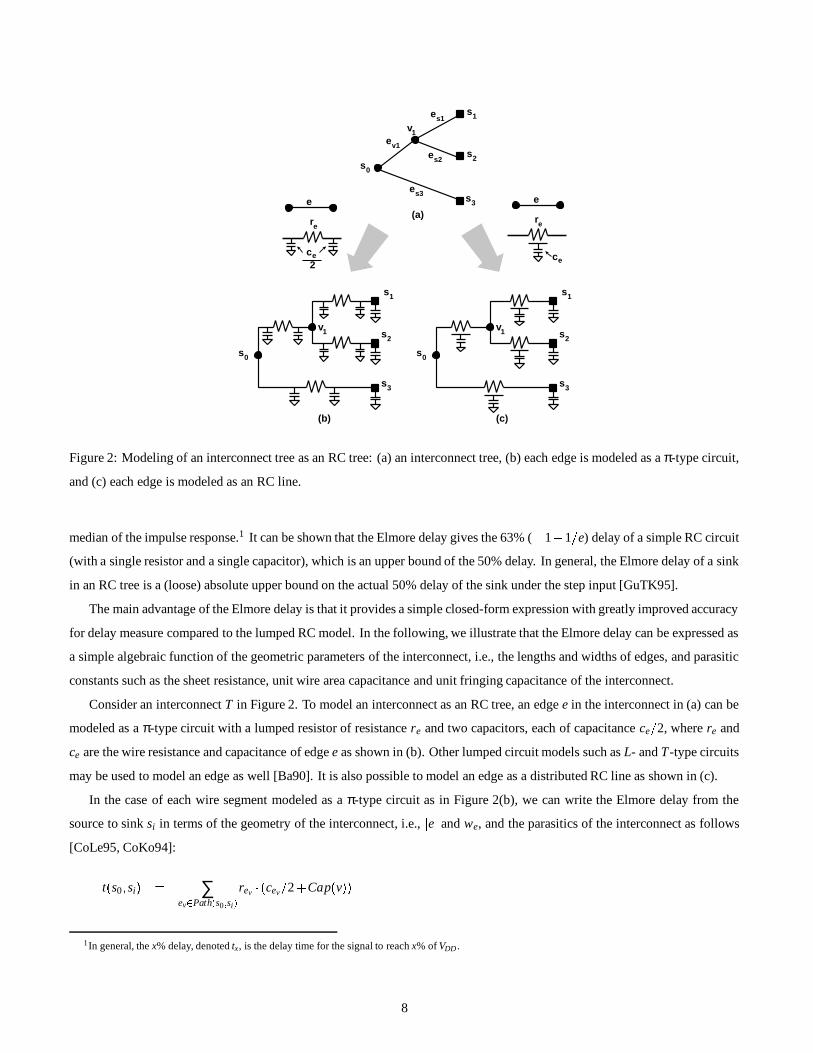
e
e
e
e
v1
s3
s1
s2
ce2
re
s1
s2
s3
v1
s0
s1
s2
s3
v1
s0
(a)
(b)
s1
s2
s3
v1
s0
(c)
e
re
e
ce
Figure 2: Modeling of an interconnect tree as an RC tree: (a) an interconnect tree, (b) each edge is modeled as a π-type circuit,
and (c) each edge is modeled as an RC line.
median of the impulse response.1 It can be shown that the Elmore delay gives the 63% ( 1 1 e) delay of a simple RC circuit
(with a single resistor and a single capacitor), which is an upper bound of the 50% delay. In general, the Elmore delay of a sink
in an RC tree is a (loose) absolute upper bound on the actual 50% delay of the sink under the step input [GuTK95].
The main advantage of the Elmore delay is that it provides a simple closed-form expression with greatly improved accuracy
for delay measure compared to the lumped RC model. In the following, we illustrate that the Elmore delay can be expressed as
a simple algebraic function of the geometric parameters of the interconnect, i.e., the lengths and widths of edges, and parasitic
constants such as the sheet resistance, unit wire area capacitance and unit fringing capacitance of the interconnect.
Consider an interconnect T in Figure 2. To model an interconnect as an RC tree, an edge e in the interconnect in (a) can be
modeled as a π-type circuit with a lumped resistor of resistance re and two capacitors, each of capacitance ce 2, where re and
ce are the wire resistance and capacitance of edge e as shown in (b). Other lumped circuit models such as L- and T-type circuits
may be used to model an edge as well [Ba90]. It is also possible to model an edge as a distributed RC line as shown in (c).
In the case of each wire segment modeled as a π-type circuit as in Figure 2(b), we can write the Elmore delay from the
source to sink si in terms of the geometry of the interconnect, i.e., e and we, and the parasitics of the interconnect as follows
[CoLe95, CoKo94]:
t s0 si ∑ev
Path s0 si rev cev 2 Cap v
1In general, the x% delay, denoted tx, is the delay time for the signal to reach x% of VDD .
8
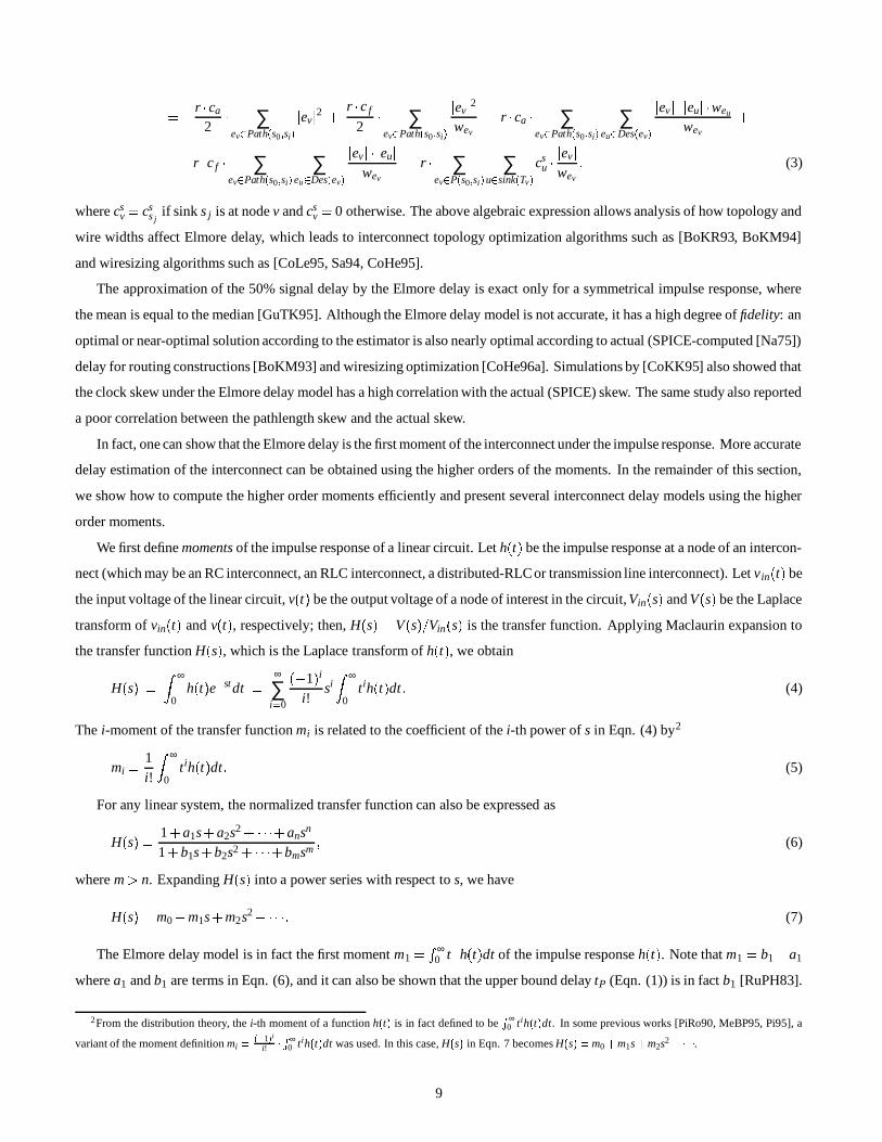
r ca
2 ∑ev
Path s0 si
ev 2 r c f
2 ∑ev
Path s0 si
ev 2wev
r ca ∑ev
Path s0 si
∑eu
Des ev
ev eu weu
wev
r c f ∑ev
Path s0 si
∑eu
Des ev
ev eu wev
r ∑ev
P s0 si
∑u
sink Tv
csu
ev wev
(3)
where csv cs
s jif sink s j is at node v and cs
v 0 otherwise. The above algebraic expression allows analysis of how topology and
wire widths affect Elmore delay, which leads to interconnect topology optimization algorithms such as [BoKR93, BoKM94]
and wiresizing algorithms such as [CoLe95, Sa94, CoHe95].
The approximation of the 50% signal delay by the Elmore delay is exact only for a symmetrical impulse response, where
the mean is equal to the median [GuTK95]. Although the Elmore delay model is not accurate, it has a high degree of fidelity: an
optimal or near-optimal solution according to the estimator is also nearly optimal according to actual (SPICE-computed [Na75])
delay for routing constructions [BoKM93] and wiresizing optimization [CoHe96a]. Simulations by [CoKK95] also showed that
the clock skew under the Elmore delay model has a high correlation with the actual (SPICE) skew. The same study also reported
a poor correlation between the pathlength skew and the actual skew.
In fact, one can show that the Elmore delay is the first moment of the interconnect under the impulse response. More accurate
delay estimation of the interconnect can be obtained using the higher orders of the moments. In the remainder of this section,
we show how to compute the higher order moments efficiently and present several interconnect delay models using the higher
order moments.
We first define moments of the impulse response of a linear circuit. Let h t be the impulse response at a node of an intercon-
nect (which may be an RC interconnect, an RLC interconnect, a distributed-RLCor transmission line interconnect). Let v in t be
the input voltage of the linear circuit, v t be the output voltage of a node of interest in the circuit, Vin s and V s be the Laplace
transform of vin t and v t , respectively; then, H s V s Vin s is the transfer function. Applying Maclaurin expansion to
the transfer function H s , which is the Laplace transform of h t , we obtain
H s ∞
0h t e stdt
∞
∑i 0
1 ii!
si ∞
0tih t dt (4)
The i-moment of the transfer function mi is related to the coefficient of the i-th power of s in Eqn. (4) by2
mi 1i!
∞
0tih t dt (5)
For any linear system, the normalized transfer function can also be expressed as
H s 1 a1s a2s2 ansn
1 b1s b2s2 bmsm (6)
where m n. Expanding H s into a power series with respect to s, we have
H s m0 m1s m2s2 (7)
The Elmore delay model is in fact the first moment m1 ∞0 t h t dt of the impulse response h t . Note that m1 b1 a1
where a1 and b1 are terms in Eqn. (6), and it can also be shown that the upper bound delay tP (Eqn. (1)) is in fact b1 [RuPH83].
2From the distribution theory, the i-th moment of a function h t is in fact defined to be ∞0 tih t dt. In some previous works [PiRo90, MeBP95, Pi95], a
variant of the moment definition mi 1 ii! ∞
0 tih t dt was used. In this case, H s in Eqn. 7 becomes H s m0 m1s m2s2 .
9
Several approaches have been proposed to compute the moments at each node of a lumped RLC tree, where the lumped
resistors and lumped inductors are floating from the ground and form a tree, and the lumped capacitors are connected between
the nodes on the tree and the ground [KaMu95, RaPi94, YuKu95b].
In the following, we present a method proposed by Yu and Kuh [YuKu95b] for moment computation in an RLC tree. Con-
sider a lumped RLC tree with n nodes. Let k be the parent node of node k, and Tk be the subtree rooted at node k. Let Ck be the ca-
pacitance connected to node k, Rk and Lk be the resistance and inductance of the branch between k and k. Let Hk s Vk s Vin s be the transfer function at node k, where Vk s is the Laplace transform of the output voltage at k, denoted vk t . Let ik t be the
current flowing from k to k, then its Laplace transform Ik s is given by [YuKu95b]:
Ik s ∑j
Tk
C j s V j s (8)
Let Rki and Lki be the total resistance and inductance on the portionof the path Path s0 i that is common with the path Path s0 k ,respectively; then, the total impedance along the common portion of paths Path s0 i and Path s0 k is Zki Rki s Lki. The
voltage drop from root s0 to node k is [YuKu95b]:
Vin s Vk s ∑i
Zki Ci s Vi s (9)
Then, the transfer function Hk s Vk s Vin s becomes [YuKu95b]:
Hk s 1 ∑i
Zki Ci s Hi s (10)
Let mpk be the p-th order moment of Hk s . Expanding Hk s and Hi s in Eqn. (10) by the expression in Eqn. (7), and equating
the coefficients of powers of s, the p-th order moment at node k under a step input can be expressed as [YuKu95b]:
mpk
0 if p 1,
1 if p 0,
∑i Rki Ci mp 1i Lki Ci mp 2
i if p 0.
(11)
Let CpTk ∑ j
Tk
mpj C j, which is the total p-th order weighted capacitance of Tk , then mp
k (for p 0) can be written recursively
as [YuKu95b]:
mpk
0 if k is the root s0 ,
mpk Rk Cp 1
Tk Lk Cp 2Tk
if k s0 .(12)
Therefore, given the p 1 -th order and p 2 -th order moments, the p-th order moments of all nodes can be computed by
first computing Cp 1Tk
and Cp 2Tk
in O n time in a bottom-up fashion. Then, mpk can be computed in a top-down fashion for all
nodes in the interconnect tree in O n time. Therefore, the moments up to the p-th order of an RLC tree can be computed in
O np time.
For moment computation of a tree of transmission lines, several works first model each transmission line as a large number
of uniform lumped RLC segments [PiRo90, SrKa94] and then compute the moments of the resulting RLC tree. However, this
approach is usually not efficient nor accurate. Kahng and Muddu [KaMu94] showed that using 10 uniform segments to approx-
imate the behavior of a transmission line entails errors in the first and second moments of around 10% and 20%, respectively. In
[KaMu94, YuKu95b], the authors improve both accuracy and efficiency by considering non-uniform segmentation of the trans-
mission line. Yu and Kuh [YuKu95b] found that for exact moment computation of up to the p-th order, each transmission line
10
should be modeled by 3p 2 non-uniform lumped RLC segments. Combining the non-uniform lumped RLC segment model
by [KaMu94, YuKu95b] with the moment computation algorithm by [YuKu95b], the moments of a transmission line tree inter-
connect up to the order of p can be computed in O np2 time, where n is the number of nodes in the tree. Another work of Yu and
Kuh [YuKu95a] computes the moments of a transmission line tree interconnect directly, without first performing non-uniform
segmentation of the transmission lines. This algorithm also has a computational complexity of O np2 .Higher order moments are extremely useful for circuit analysis. In general, higher order moments can be used to improve the
accuracy of delay estimation. For example, Krauter et al. [KrGW95] proposed metrics based on the first three central moments,
which are the moments of the distribution of the impulse response. From the distribution theory, the second central moment
provides a measure of the spread of h t and the third central moment measures the skewness of h t . Since the accuracy of
the Elmore delay is affected by the spread and skewness of the impulse distribution, the three central moments may be used to
reduce the relative errors of Elmore delay [GuTK95].3
Another advantage of using higher order moments for circuit analysis is that it can handle the inductance effect. When the
operating frequencies of VLSI circuits are in the giga-hertz range and the dimension of interconnect is comparable to the signal
wavelength, inductance plays a significant role in signal delay and signal integrity. An inherent shortcoming of the Elmore delay
model and other simpler delay models is that they cannot handle the inductance effect.
The Asymptotic Waveform Evaluation (AWE) method proposed by Pillage and Rohrer [PiRo90] is an efficient technique to
use higher order moments in interconnect timing analysis which can handle the inductance effect. It constructs a q-pole transfer
function H s , called the q-pole model,
H s q
∑i 1
ki
s pi (13)
to approximate the actual transfer function H s , where pi are poles and ki are residues to be determined. The corresponding
time domain impulse response is
h t q
∑i 1
kiepit (14)
The poles and residues in H s can be determined uniquely by matching the initial boundary conditions, denoted m 1 , and the
first 2q 1 moments mi of H s to those of H s [PiRo90]. The choice of order q depends on the accuracy required but is always
much less than the order of the circuit. In practice, q 5 is commonly used.
When q is chosen to be two, it is known as the two-pole model [Ho84, ZhTG93, GaZh93, ZhST93, ZhST94]. In this model,
the first three moments m0 (which is normalized), m1, and m2 are used. A closed-form expression of m2 is given and an analytical
formula relating the performance of an RLC interconnect to its topology and geometry is derived by Gao and Zhou [GaZh93].
This provides a closed-form formula for the topology optimization algorithm in [ZhTG93]. However, the expression of m2 is
much more complicated than that of m1 (the Elmore delay). Moreover, the method of [Ho84, GaZh93, ZhST94] calculates the
second moment by replacing the off-path admittance by the sum of the total subtree capacitance. This is correct only to the
coefficient of s in the subtree admittance. Thus, such a method underestimates the subtree impedance. As a result, the response
obtained is a lower bound of the actual response, and the delay estimate is an upper bound on the actual delay. To compute the
3The three moments were also used to detect underdamping, determine the conditions of critical damping for series terminated transmission line nets, and
estimate the delay of the properly terminated line [KrGW95].
11

second moment exactly, the admittance of off-path subtrees must be calculated correctly up to the coefficient of s2 . This was
done in [KaMu95, KaMu96b, YuKu95b].
Based on the two-pole methodology, Kahng and Muddu [KaMu96b] derived an analytical delay model for RLC intercon-
nects. Consider a source driving a distributed RLC line with total resistance RL, total inductance LL, and total capacitance CL.
The source is modeled as a resistive and inductive impedance (Zd Rd s Ld). The load CT at the end of the RLC line is
modeled as a capacitive impedance (ZT 1s CT
). The transfer function is truncated to be [KaMu96b]
H s 11 b1s b2s2 (15)
where
b1 RdCL RLCT RLCL
2 RLCT
b2 RdRLC2L
6 Rd RLCLCT
2 RLCL 2
24 R2
LCLCT
6 LdCL LdCT LLCL
2 LLCT
The first and second moments m1 and m2 can be obtained from b1 and b2, i.e., m1 b1 and m2 b21 b2. The authors separately
derive the sink delay at the load CT , denoted tT , from the two-pole response depending on the sign of b21 4b2 [KaMu96b]:
tT
Kr
m1
4m2 3m21
2 if b21 4b2 0, i.e., real poles
Kc 2 m21 m2
3m21 4m2
if b21 4b2 0, i.e., complex poles
Kd m12 if b2
1 4b2 0, i.e., double poles
where Kr, Kc, and Kd are functions of b1 and b2 as described in [KaMu96b]. The model is further extended to consider RLC
interconnection trees [KaMu96b] and ramp input [KaMM96].
While the methods in [KaMu96b, KaMM96] used only the first two moments, Tutuianu, Dartu, and Pileggi [TuDP96] pro-
posed an explicit RC-circuit delay approximation based on the first three moments of the impulse response. The model uses the
first three moments (m1 m2 and m3) to determine stable approximations of the first two dominant poles p1 and p2 of H s . By
matching the first two moments of the actual transfer function, the two residues k1 and k2 can be obtained. The explicit approxi-
mation of the delay point is a single Newton-Raphson iteration step, using the first order delay estimate (which can be expressed
in terms of the poles and residues) as the initial guess. The reader is referred to [TuDP96] for the exact expressions of p1 , p2 ,
k1 , k2, and the delay function.
2.2 Driver Delay Models
In interconnect-driven layout designs, gates/buffers need to be optimized according to the interconnect load. Moreover, the
design of a gate/buffer also affects the interconnect design and optimization considerably. It is common that each gate or buffer
has a set of implementations with varying driving capabilities. These implementations are normally characterized by input (gate)
capacitance, effective output (driver) resistance, denoted Rd , and internal delay, derived from either analytical formulas or circuit
simulation.
In the following,we collectively refer to gates, buffers and even transistorsas drivers. Given an input signal, we are interested
in modeling the response waveform of a gate, buffer, or transistor at the output of the driver. We define the fall time, denoted t f ,
12
Rn
dCCg dCCg
(a) (b)
n n
Rmin = Rp dp
= Rn dn
Figure 3: A switch-level RC model of (a) an n-transistor and (b) an inverter with equal pull-up and pull-down strength by ad-
justing the p- and n-transistor sizes dp and dn , respectively.
as the time for the response waveform to fall from 90% to 10% of its steady-state value. The delay time for the falling signal,
denoted td f , is the time difference between input transition (50%) and the 50% output level. Similarly, we can define the rise
time, denoted tr, and the delay time for the rising signal, denoted tdr . We use td to denote delay time for the signal if we do not
distinguish between rising and falling signal. In general, the input has an input transition time, denoted tt , which is the input rise
or fall time.
We first use a transistor to illustrate the simple switch-level RC model, where a transistor is modeled as an effective resistance
discharging or charging a capacitor [WeEs93]. Figure 3(a) shows a simple switch-level RC model of an n-transistor. Let the
minimum n-transistor resistance be Rn . The gate capacitance and output diffusion capacitance of the minimum n-transistor are
denoted Cng and Cn
d , respectively. We normalize the transistor size such that a minimum-size transistor has unit size.
In the simple switch-level RC model, for an n-transistor of size d 1, its effective resistance Rd is Rn d. The capacitances
are directly proportional to the transistor sizes, i.e., the gate capacitance is Cng d and the diffusion capacitance is Cn
d d. Assuming
a step input, the fall time of the signal at the gate output is given by [WeEs93]:
t f k CL
βnmin d VDD
(16)
where k is typically in the range of 3 to 4 for values of VDD in the range of 3 to 5, βnmin is the gain factor for the minimum n-
transistor, and CL is the loading capacitance driven by the transistor. The delay time for the falling signal can be approximated
to be td f t f 2 [WeEs93]. Note that since the effective resistance Rd is proportional to 1 βmin d, we can simply approximate
td f by the product of the effective transistor resistance and the loading capacitance CL. The above discussion can be applied to
a p-transistor by simply replacing the superscript n by p and the fall time by the rise time.
An inverter consists of an n-transistor and a p-transistor, and can be modeled by the simple switch-level RC model as shown
in Figure 3(b). The output capacitance of the inverter is the sum of the diffusion capacitances due to the p- and n-transistors.
Similarly, the input gate capacitance of the inverter is the sum of the gate capacitances due to both transistors. It is a common
practice to size the p- and n-transistors in the inverter to a fixed ratio, called the p/n ratio. In this case, the size of an inverter is
defined to be the scaling factor with respect to the minimum-size inverter (with the fixed p/n ratio). Other CMOS gates can be
modeled similarly.
A shortcoming of the simple RC model is that it cannot deal with the shape of the input waveform. In practice, the effective
13
resistance of a transistor depends on the waveform on its input. A sharp input transition allows the full driving power of the
driver to charge or discharge the load and therefore results in a smaller effective resistance of the driver. On the other hand, a
slow transition results in a larger effective resistance of the driver. Hedenstierna and Jeppson [HeJe87] consider input waveform
slope and provide the following expression for the delay time of a falling signal:
td f t f 2 tt6 1 2
Vnth
VDD (17)
where tt is the input transition time (more specifically, the input rise time in this case) and V nth is the threshold voltage of n-
transistor.
In the slope model (first proposed by Pillingand Skalnik [PiSk72]), a one-dimensional table for the effective driver resistance
based on the concept of rise-time ratio is proposed by Ousterhout [Ou84]. The effective resistance of a driver depends on the
transition time of the input signal, the loading capacitance, and the size of the driver. In the slope model, the output load and
transistor size are first combined into a single value called the intrinsic rise-time of the driver, which is the rise-time at the output
if the input is a step-function. The input rise-time of the driver is then divided by the intrinsic rise-time of the driver to produce
the rise-time ratio of the driver. The effective resistance is represented as a piece-wise linear function of the rise-time ratio and
stored in a one-dimensional table. Given a driver, one first computes its rise-time ratio and then calculates its effective resistance
Rd by interpolation according to its rise-time ratio from the one-dimensional table. The driver rise-time delay is computed by
multiplying the effective resistance with the total capacitance. Similarly, we can have a look-up table for the fall-time ratio of
the driver.
Another commonly used driver delay model pre-characterizes the driver delay of each type of gate/buffer in terms of the
input transition time tt , and the total load capacitance CL in the following form of k-factor equations [WeEs93, QiPP94]:
td f k1 k2 CL tt k3 C3L k4 CL k5 (18)
t f k 1 k 2 CL tt k 3 C2L k 4 CL k 5 (19)
where k1 5 and k 1 5 are determined based on detailed circuit simulation (e.g. using SPICE [Na75]) and linear regression or
least square fits. Similar k-factor equations can be obtained for the delay and rise time of the rising output transition.
More generally, a look-up table can be used to characterize the delay of each type of gate. A typical entry in the table can be
of the followingform: td f t f tt CL . Given an input transition time tt and an output loading capacitance, the look-up table for
a specific gate provides the delay and rise/fall time. The table look-up approach can be very accurate, but it is costly to compute
and store a multi-dimensional table.
All these driver delay models use the loading capacitance for delay computation. In the first order approximation, the loading
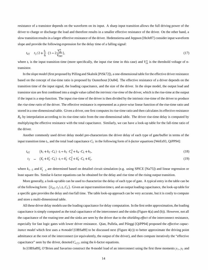
capacitance is simply computed as the total capacitance of the interconnect and the sinks (Figure 4(a) and (b)). However, not all
the capacitance of the routing tree and the sinks are seen by the driver due to the shielding effect of the interconnect resistance,
especially for fast logic gates with lower driver resistance. Qian, Pullela, and Pileggi [QiPP94] proposed the effective capac-
itance model which first uses a π-model [OBSa89] to be discussed next (Figure 4(c)) to better approximate the driving point
admittance at the root of the interconnect (or equivalently, the output of the driver), and then compute iteratively the “effective
capacitance” seen by the driver, denoted Ce f f , using the k-factor equations.
In [OBSa89], O’Brien and Savarino construct the π-model load of an interconnect using the first three moments y1 , y2 and
14
(a)
(b)
(c)
(d)
C
C
C
C
R
12
eff
total
t t
t t
t t
t t
Figure 4: (a) An inverter driving an RC interconnect. (b) The same inverter driving the total capacitance of the net in (a). (c) A
π-model of the driving point admittance for the net in (a). (d) The same inverter driving the effective capacitance of the net in
(a). The input signal has a transition time of tt .
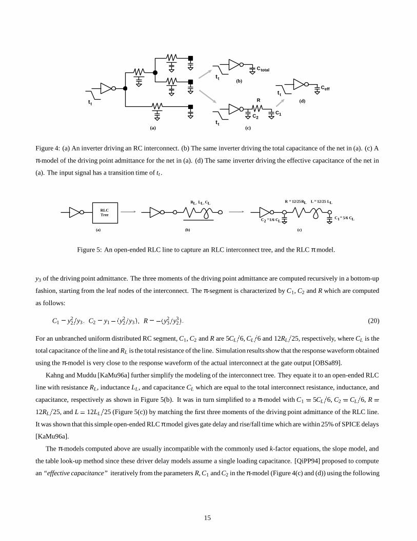
RLCTree
CLLRL L, ,
C1
R L
5/6
12/25 12/25
1/6
= =
= = CLCLC2
LLRL
(a) (b) (c)
Figure 5: An open-ended RLC line to capture an RLC interconnect tree, and the RLC π model.
y3 of the driving point admittance. The three moments of the driving point admittance are computed recursively in a bottom-up
fashion, starting from the leaf nodes of the interconnect. The π-segment is characterized by C1, C2 and R which are computed
as follows:
C1 y22 y3 C2 y1 y2
2 y3 R y23 y3
2 (20)
For an unbranched uniform distributed RC segment, C1, C2 and R are 5CL 6, CL 6 and 12RL 25, respectively, where CL is the
total capacitance of the line and RL is the total resistance of the line. Simulation results show that the response waveform obtained
using the π-model is very close to the response waveform of the actual interconnect at the gate output [OBSa89].
Kahng and Muddu [KaMu96a] further simplify the modeling of the interconnect tree. They equate it to an open-ended RLC
line with resistance RL, inductance LL , and capacitance CL which are equal to the total interconnect resistance, inductance, and
capacitance, respectively as shown in Figure 5(b). It was in turn simplified to a π-model with C1 5CL 6, C2 CL 6, R 12RL 25, and L 12LL 25 (Figure 5(c)) by matching the first three moments of the driving point admittance of the RLC line.
It was shown that this simple open-ended RLC π model gives gate delay and rise/fall time which are within 25% of SPICE delays
[KaMu96a].
The π-models computed above are usually incompatible with the commonly used k-factor equations, the slope model, and
the table look-up method since these driver delay models assume a single loading capacitance. [QiPP94] proposed to compute
an “effective capacitance” iteratively from the parameters R, C1 and C2 in the π-model (Figure 4(c) and (d)) using the following
15
expression:
Ce f f C2 C1 1
R C1
tD tx 2 R C1 2
tx tD tx 2 e tD tx
R C1 1 e txR C1 (21)
where tD td f tt 2 and tx tD t f 2, and td f and t f can both be obtained from the k-factor equations in terms of the effective
capacitance and the input transition tt . The iteration starts with using the total interconnect and sink capacitance as the loading
capacitance CL to get an estimate of tD and tx through the k-factor equations. A better estimate of the effective capacitance is
computed using Eqn. (21) and it is used as the loading capacitance for the next iteration of computation. The process stops when
the value of Ce f f does not change in two successive iterations.
[QiPP94] also observes that the slow decaying tail portion of the response waveform is not accurately captured by the ef-
fective capacitance model. This is due to the CMOS gate behaving like a resistor to ground beyond some timepoint ts, and its
interaction with a π-model load yielding a vastly different response than the effective capacitance. Therefore, [QiPP94] uses the
effective capacitance model to capture the initial delay and a resistance model (R-model) to capture the remaining portion of the
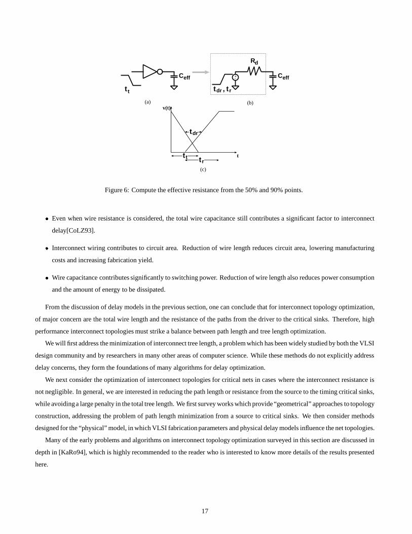
response. They calculate the effective driver resistance by [QiPP94] (Figure 6):
Rd t80 ts
Ce f f ln v ts v t80
(22)
where t80 is the 80% point delay computed by the k-factor equations and v ts can be estimated from the Ce f f model. The com-
putation of ts is given in [QiPP94]. Then, the voltage response at the gate output after time ts can be expressed as a double
exponential approximation [QiPP94]:
v2 t α1ep1 t ts α2ep2 t ts (23)
where α1, α2, p1, and p2 can be obtained from Rd , the π-model parameters (R, C1, and C2), and the initial conditions on the
π-model as described in [QiPP94]. Note that the driver resistance Rd , together with tdr and tr (or td f and t f ) computed by the k-
factor equations, and the RC interconnect, can be used to estimate the input transition time and delay for the sinks using models
described in Section 2.1.
The models described above are used mostly in the works on wiresizing optimization since an accurate estimate of the driver
resistance prevents oversizing of the wire widths. They are also crucial in the works that consider sizing of drivers, together with
the optimization of the interconnect.
3 Topology Optimization for High Performance Interconnect
In this section we address the problem of topology optimization for high performance interconnect. Two major design goals
must be considered for this problem: the minimization of total interconnect wire length, and the minimization of path length or
signal delay from a driver to one or several timing-critical sinks.
Wire length minimization is of interest for the following reasons.
When the wire resistance is negligible compared to the driver resistance, minimization of total wire capacitance (and
hence, net wire length) provides near optimal performance with respect to delay[CoLZ93].
16
Ceff +- Ceff
Rd
t t tdr tr,
v(t)
t
tdr
t t tr
(a) (b)
(c)
Figure 6: Compute the effective resistance from the 50% and 90% points.
Even when wire resistance is considered, the total wire capacitance still contributes a significant factor to interconnect
delay[CoLZ93].
Interconnect wiring contributes to circuit area. Reduction of wire length reduces circuit area, lowering manufacturing
costs and increasing fabrication yield.
Wire capacitance contributes significantly to switching power. Reduction of wire length also reduces power consumption
and the amount of energy to be dissipated.
From the discussion of delay models in the previous section, one can conclude that for interconnect topology optimization,
of major concern are the total wire length and the resistance of the paths from the driver to the critical sinks. Therefore, high
performance interconnect topologies must strike a balance between path length and tree length optimization.
We will first address the minimization of interconnect tree length, a problem which has been widely studied by both the VLSI
design community and by researchers in many other areas of computer science. While these methods do not explicitly address
delay concerns, they form the foundations of many algorithms for delay optimization.
We next consider the optimization of interconnect topologies for critical nets in cases where the interconnect resistance is
not negligible. In general, we are interested in reducing the path length or resistance from the source to the timing critical sinks,
while avoidinga large penalty in the total tree length. We first survey works which provide “geometrical” approaches to topology
construction, addressing the problem of path length minimization from a source to critical sinks. We then consider methods
designed for the “physical” model, in which VLSI fabrication parameters and physical delay models influence the net topologies.
Many of the early problems and algorithms on interconnect topology optimization surveyed in this section are discussed in
depth in [KaRo94], which is highly recommended to the reader who is interested to know more details of the results presented
here.
17
3.1 Topology Optimization for Total Wirelength Minimization
A problem central to any area of interconnect optimization is the minimization of the wirelength of a net. Research on the
construction of Minimum Spanning Trees (MST) and Steiner Minimal Trees (SMT) is directly applicable to problems in VLSI
interconnect design. Note that we use the abbreviation SMT for Steiner Minimal Trees to avoid ambiguity with the abbreviation
MST.
3.1.1 Minimum Spanning Trees
The MST problem involves finding a set of edges E which connect a given set of points P with minimum total cost. Two classic
algorithms solve this problem optimally. Kruskal’s algorithm[Kr56] begins with a forest of trees (the singleton vertices), and
iteratively adds the lowest cost edge which connects two trees in the current forest (forming a new tree), until only a single
tree which connects all points in P remains. Prim’s algorithm[Pr57] starts with an arbitrary node as the root of a partial tree,
and grows the partial tree by iteratively adding an unconnected vertex to it using the lowest cost edge, until no unconnected
vertex remains. Both algorithms construct MSTs with the minimum total cost. For a problem with n vertices, we can construct a
Voronoi diagram[LeWo80] to constrain the number of edges to be considered by the two algorithms to be linear with n. With this
constraint on the number of edges, both algorithms can be made to run in O nlogn time. Naive implementations have slightly
higher complexity. We use MST P to denote the minimum spanning tree of point set P.
3.1.2 Conventional Steiner Tree Algorithms
MST constructions are restricted to direct connections between the pins of a net, which is not necessary in VLSI design. Inter-
connect topology construction is in fact a rectilinear Steiner tree problem, which has been studied extensively outside the VLSI
design community, and goes well beyond the scope of this paper. We will discuss several typical and commonly used algorithms
here, and recommend a more detailed survey by Hwang and Richards[HwRi92] to the interested reader.
The Steiner problem is defined as follows: Given a set P of n points, find a set S of Steiner points such that MST P S has
the minimum cost. For interconnect optimization problems, the set P consists of the pins of a net. Note that the inclusion of
additional points to the spanning tree can reduce the total tree length.
While the MST problem can be solved optimally in polynomial time, construction of a SMT is NP-hard for graphs, and for
both rectilinear and Euclidean distance metrics[GaJo79]. We shall present several effective SMT heuristics for the rectilinear
distance metric, which is most relevant to VLSI interconnect design.
Clearly the set of potential Steiner points is infinite. For the rectilinear metric, however, Hanan[Ha66] showed that the set
of Steiner points which need to be considered in the construction of a SMT can be limited to the “Hanan grid,” formed by the
intersections of vertical and horizontal lines through the vertices of the initial point set. Given this observation, optimal SMT
algorithms which utilize branch-and-bound techniques can be constructed, but these algorithmshave exponential complexity and
are applicable to only small problems. Given that construction of an optimal SMT is NP-hard, it is natural to look for heuristics.
An interesting result, due to Hwang[Hw76], is that the ratio of tree lengths between a rectilinear MST and a rectilinear SMT is no
worse than 32 . The bounded performance of MST constructions has made the Prim and Kruskal algorithms popular as the basis
of Steiner tree heuristics. We choose to present three general heuristic approaches which are effective and commonly used for
18
SMT construction. One approach uses “edge merges,” a second involves iterative Steiner point insertion, and a third involves
iterative edge insertion and cycle removal.
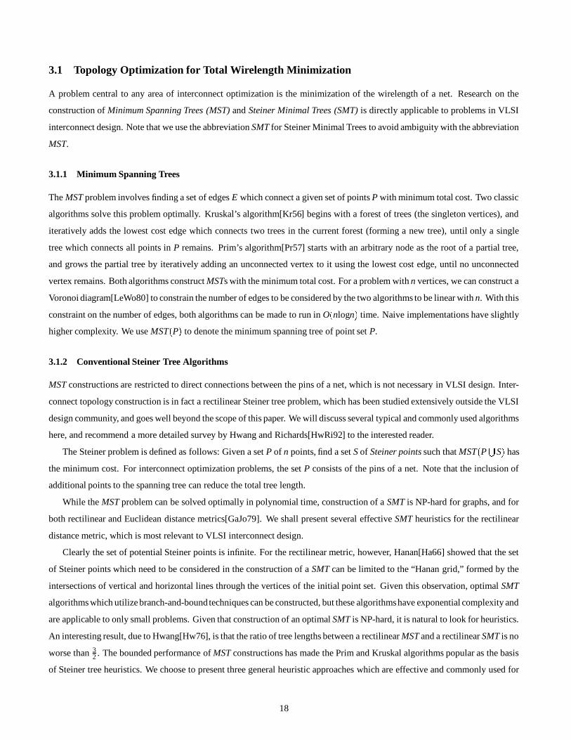
Many Steiner tree heuristics follow the general approach of improving an initial Minimum Spanning Tree by a series of edge
merges. For a pair of adjacent edges in a spanning tree, there is the possibility that by merging portions of the two edges, tree
length can be reduced. An example of this is shown in Figure 7. There may be more than one way in which edges can be merged;
the selection of edges and the order of their merging is a central concern of many Steiner tree heuristics.
Figure 7: A conventional spanning tree improvement through the merging of edges.
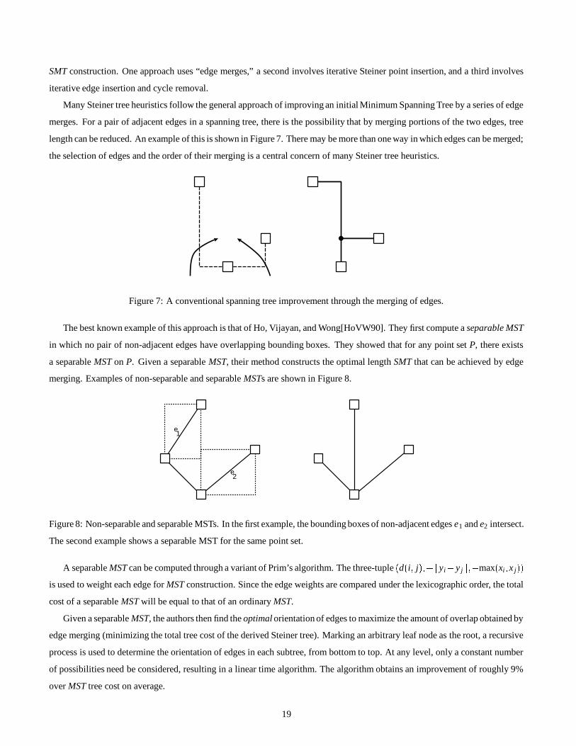
The best known example of this approach is that of Ho, Vijayan, and Wong[HoVW90]. They first compute a separable MST
in which no pair of non-adjacent edges have overlapping bounding boxes. They showed that for any point set P, there exists
a separable MST on P. Given a separable MST, their method constructs the optimal length SMT that can be achieved by edge
merging. Examples of non-separable and separable MSTs are shown in Figure 8.
e1
e2
Figure 8: Non-separable and separable MSTs. In the first example, the bounding boxes of non-adjacent edges e1 and e2 intersect.
The second example shows a separable MST for the same point set.
A separable MST can be computed through a variant of Prim’s algorithm. The three-tuple d i j yi y j max xi x j is used to weight each edge for MST construction. Since the edge weights are compared under the lexicographic order, the total
cost of a separable MST will be equal to that of an ordinary MST.
Given a separable MST, the authors then find the optimal orientation of edges to maximize the amount of overlap obtained by
edge merging (minimizing the total tree cost of the derived Steiner tree). Marking an arbitrary leaf node as the root, a recursive
process is used to determine the orientation of edges in each subtree, from bottom to top. At any level, only a constant number
of possibilities need be considered, resulting in a linear time algorithm. The algorithm obtains an improvement of roughly 9%
over MST tree cost on average.
19
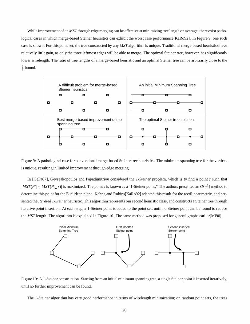
While improvement of an MST through edge merging can be effective at minimizing tree length on average, there exist patho-
logical cases in which merge-based Steiner heuristics can exhibit the worst case performance[KaRo92]. In Figure 9, one such
case is shown. For this point set, the tree constructed by any MST algorithm is unique. Traditional merge-based heuristics have
relatively little gain, as only the three leftmost edges will be able to merge. The optimal Steiner tree, however, has significantly
lower wirelength. The ratio of tree lengths of a merge-based heuristic and an optimal Steiner tree can be arbitrarily close to the32 bound.
A difficult problem for merge-basedSteiner heuristics.
An initial Minimum Spanning Tree
Best merge-based improvement of thespanning tree.
The optimal Steiner tree solution.
Figure 9: A pathological case for conventional merge-based Steiner tree heuristics. The minimum spanning tree for the vertices
is unique, resulting in limited improvement through edge merging.
In [GePa87], Georgakopoulos and Papadimitriou considered the 1-Steiner problem, which is to find a point s such that
MST P - MST P s is maximized. The point s is known as a “1-Steiner point.” The authors presented an O n2 method to
determine this point for the Euclidean plane. Kahng and Robins[KaRo92] adapted this result for the rectilinear metric, and pre-
sented the Iterated 1-Steiner heuristic. This algorithm represents our second heuristic class, and constructs a Steiner tree through
iterative point insertion. At each step, a 1-Steiner point is added to the point set, until no Steiner point can be found to reduce
the MST length. The algorithm is explained in Figure 10. The same method was proposed for general graphs earlier[Mi90].
First insertedSteiner point
Second insertedSteiner point
Initial MinimumSpanning Tree
Figure 10: A 1-Steiner construction. Starting from an initial minimum spanning tree, a single Steiner point is inserted iteratively,
until no further improvement can be found.
The 1-Steiner algorithm has very good performance in terms of wirelength minimization; on random point sets, the trees
20
generated by this algorithm are 11% shorter than MSTs on average. The best possible possible improvement is conjectured to
be roughly 12% on average[Be88], so the 1-Steiner algorithm is considered to be very close to optimal. While this algorithm
constructs trees which are close to optimal in terms of length, it suffers from relatively high complexity. A sophisticated im-
plementation is O n3 , while a naive approach may be O n5 ; this may make it impractical for problems with large numbers of
vertices.
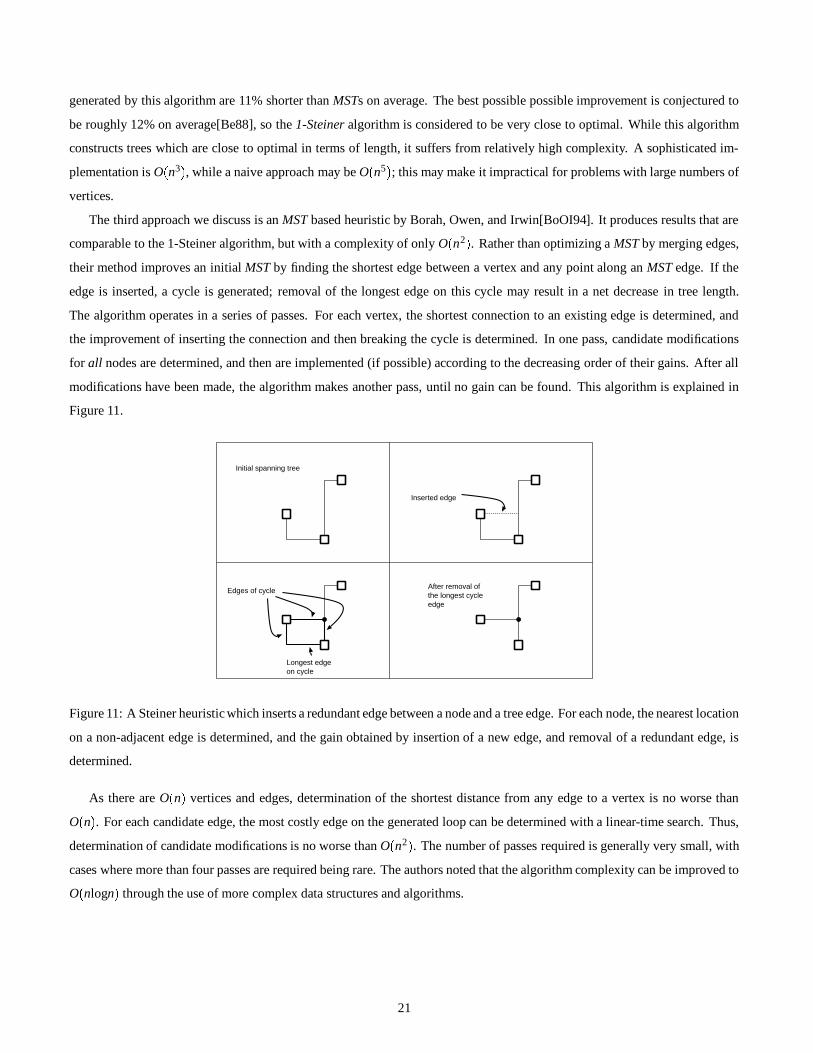
The third approach we discuss is an MST based heuristic by Borah, Owen, and Irwin[BoOI94]. It produces results that are
comparable to the 1-Steiner algorithm, but with a complexity of only O n2 . Rather than optimizing a MST by merging edges,
their method improves an initial MST by finding the shortest edge between a vertex and any point along an MST edge. If the
edge is inserted, a cycle is generated; removal of the longest edge on this cycle may result in a net decrease in tree length.
The algorithm operates in a series of passes. For each vertex, the shortest connection to an existing edge is determined, and
the improvement of inserting the connection and then breaking the cycle is determined. In one pass, candidate modifications
for all nodes are determined, and then are implemented (if possible) according to the decreasing order of their gains. After all
modifications have been made, the algorithm makes another pass, until no gain can be found. This algorithm is explained in
Figure 11.
Edges of cycle
Longest edgeon cycle
Inserted edge
After removal ofthe longest cycleedge
Initial spanning tree
Figure 11: A Steiner heuristic which inserts a redundant edge between a node and a tree edge. For each node, the nearest location
on a non-adjacent edge is determined, and the gain obtained by insertion of a new edge, and removal of a redundant edge, is
determined.
As there are O n vertices and edges, determination of the shortest distance from any edge to a vertex is no worse than
O n . For each candidate edge, the most costly edge on the generated loop can be determined with a linear-time search. Thus,
determination of candidate modifications is no worse than O n2 . The number of passes required is generally very small, with
cases where more than four passes are required being rare. The authors noted that the algorithm complexity can be improved to
O nlogn through the use of more complex data structures and algorithms.
21
3.2 Topology Optimization for Path Length Minimization
If we wish to reduce the delay from a net driver to a critical sink, and the interconnect resistance between the two is significant,
an obvious approach is to reduce this resistance. Assuming uniform wire width, constraining path lengths between source and
sink clearly realizes this goal.
In this subsection, we discuss approaches to delay minimization through the “geometric” objective of path length reduction
or minimization.
3.2.1 Tree Cost/Path Length Tradeoffs
Cohoon and Randal[CoRa91] presented an early work which addressed the problem of constructing interconnect trees for the
VLSI domain, considering path length while not requiring shortest paths. Their heuristic method attempts to construct a Max-
imum Performance Tree (MPT), defined as a tree which has minimum total length among trees with optimized source-to-sink
path lengths. Their method consists of three basic steps: trunk generation, net completion, and tree improvement.
In their study, the authors observed that trees which had relatively low path lengths usually had “trunks,” monotonic paths
from the source to distant sinks. Other sink vertices generally were connected to a trunk at a nearby location. Trunk generation
consists of constructing paths from the source to the most distant sinks. Five methods of trunk generation were studied. Four
involve the insertionof an S-shaped three segment monotonic path from the source to a distant sink. The middle segment location
is determined by finding either the mean or median of the point set. The fifth method constructs trunks by building a rectilinear
shortest path tree on the graph, and then keeping the paths derived for the most distant sinks as the basis of the MPT.
Net completion involves the attachment of the remaining sink vertices to the trunks that have been formed. The authors use
three techniques: a rectilinear MST (RMST) algorithm, a rectilinear Shortest Path Tree (RSPT) algorithm, and a hybrid of the
two. The hybrid works as follows: if the RMST connection of a sink does not result in a path length greater than the radius of
the net, the connection is used; otherwise, an RSPT connection is used. For each connection, the edge routing which results in
the maximum overlap with the existing tree is selected, and the edges are merged.
Tree improvement involves a series of edge merges (similar to the merge-based Steiner tree heuristics of [HoVW90], de-
scribed in Section 3.1.2) and edge insertions and deletions. The operations are performed such that the path length from the
source to the most distant sink is not increased, and this phase terminates at the local optimum. In experiments with a variety of
point sets, the authors observed that their heuristic produced an average of 25% reductions in path length with increases of 6%
in wire length, when compared to the Steiner tree heuristic of [HoVW90].
While the MPT algorithm provides a measure of control over the tradeoff between path length and tree length, a number of
authors have attempted to refine this control. Some algorithms are able to bound the maximum tree length, the maximum path
length, or both, with constant factors.
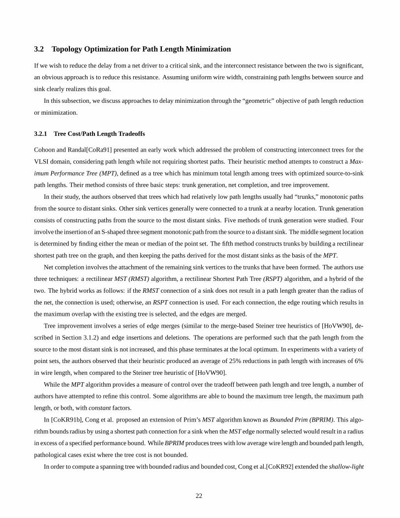
In [CoKR91b], Cong et al. proposed an extension of Prim’s MST algorithm known as Bounded Prim (BPRIM). This algo-
rithm bounds radius by using a shortest path connection for a sink when the MST edge normally selected would result in a radius
in excess of a specified performance bound. While BPRIM produces trees with low average wire length and bounded path length,
pathological cases exist where the tree cost is not bounded.
In order to compute a spanning tree with bounded radius and bounded cost, Cong et al.[CoKR92] extended the shallow-light
22

tree construction by Awerbuch, Baratz, and Peleg [AwBP90], which was originallydesigned for communications protocols. The
algorithm of [AwBP90] constructs spanning trees which have bounded performance for both total tree length and also maximum
diameter. This class of constructions are known as shallow-light trees. Total tree length for their algorithm is at most 2 2ε
times that of a minimum spanning tree, while the diameter is at most 1 2ε times that of the diameter of the pointset. The ε
parameter may be adjusted freely, allowing a preference for either tree length or diameter.
The Bounded Radius Bounded Cost (BRBC) spanning tree of [CoKR92] uses the shallow-light approach, and works as fol-
lows.
1. Construct an MST TM and an SPT TS for the graph.
2. Perform a depth-first traversal of TM. This traversal defines a tour of the tree, and each edge is traversed exactly twice.
3. Construct a “line-version” L of TM, which is a path graph containing the vertices in the order that they were visited during
depth-first traversal. Note that each vertex appears twice in L, and that the cost of L is at most twice the total cost of TM.
4. Construct a graph Q by traversing L. A running total of the distance in Q from the source is maintained; if the distance
exceeds 1 ε times the radius, a shortest path from s0 to the current vertex is inserted.
5. Construct a shortest path tree T in Q.
The resulting tree has length no greater than 1 2ε times that of a minimum spanning tree, and radius no greater than 1 ε
times that of a shortest path tree. An example of tree construction using the BRBC method is shown in Figure 12. Khuller,
Raghavachari, and Young[KhRY93] developed a method similar to BRBC contemporaneously.
Alpert et al.[AlHK93] proposed AHHK trees as a direct trade-off between Prim’s MST algorithm and Dijkstra’s shortest path
tree algorithm. They utilize a parameter 0 c 1 to adjust the preference between tree length and path length. Their algorithm
iteratively adds an edge epq between vertices p T and q T , where p and q minimize c dT s0 p d p q .The authors showed that their AHHK tree has radius no worse than c times the radius of a shortest path tree. For pathological
cases in general graphs, their tree may have unbounded cost with respect to a minimum spanning tree. They conjectured that
the cost ratio may be bounded when the problem is embedded in a rectilinear plane.
Most of the algorithms presented in this subsection so far are focused on bounded radius spanning tree construction, and
do take advantage of Steiner point generation. In [LiCW93], Lim, Cheng, and Wu proposed Performance Oriented Rectilinear
Steiner Trees for the interconnect optimization problem. Their heuristic method attempts to minimize total tree length while
satisfying distance constraints between the net driver and various sink nodes.
Their method utilizes a “Performance Oriented Spanning Tree” algorithm repeatedly during Steiner tree construction. Span-
ning tree construction proceeds in a manner similar to that of BPRIM, with edge selection being based on finding the lowest cost
edge which does not violate a distance bound by its inclusion. Note that the constructed tree is not necessarily planar, and can
have cost higher than that of an MST. The Steiner variant of their algorithm proceeds as follows. Beginning with the driver as
the root of a partial tree, the Steiner tree grows by a single Hanan grid edge from the partial tree towards a sink node. As the tree
grows, certain edges may be required for inclusion (to meet path length bounds); these edges are inserted automatically. If there
are no edges that must be included, their heuristic assigns weights to edges of the Hanan grid, and selects the edge with highest
23
An initial spanning tree. The "line" graph L, constructedby a depth first tour of the graph.
Additional edges inserted toensure radius bound.
The shortest path tree basedon the depth first tour and insertededges.
Figure 12: A Bounded-Radius Bounded-Cost construction.
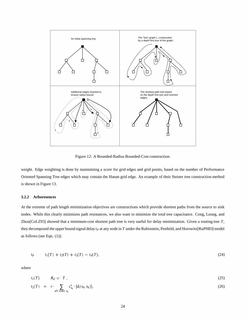
weight. Edge weighting is done by maintaining a score for grid edges and grid points, based on the number of Performance
Oriented Spanning Tree edges which may contain the Hanan grid edge. An example of their Steiner tree construction method
is shown in Figure 13.
3.2.2 Arboresences
At the extreme of path length minimization objectives are constructions which provide shortest paths from the source to sink
nodes. While this clearly minimizes path resistances, we also want to minimize the total tree capacitance. Cong, Leung, and
Zhou[CoLZ93] showed that a minimum-cost shortest path tree is very useful for delay minimization. Given a routing tree T ,
they decomposed the upper bound signal delay tP at any node in T under the Rubinstein, Penfield, and Horowitz[RuPH83] model
as follows (see Eqn. (1)):
tP t1 T t2 T t3 T t4 T (24)
where
t1 T Rd c T (25)
t2 T r ∑all sinks sk
cssk dt s0 sk (26)
24
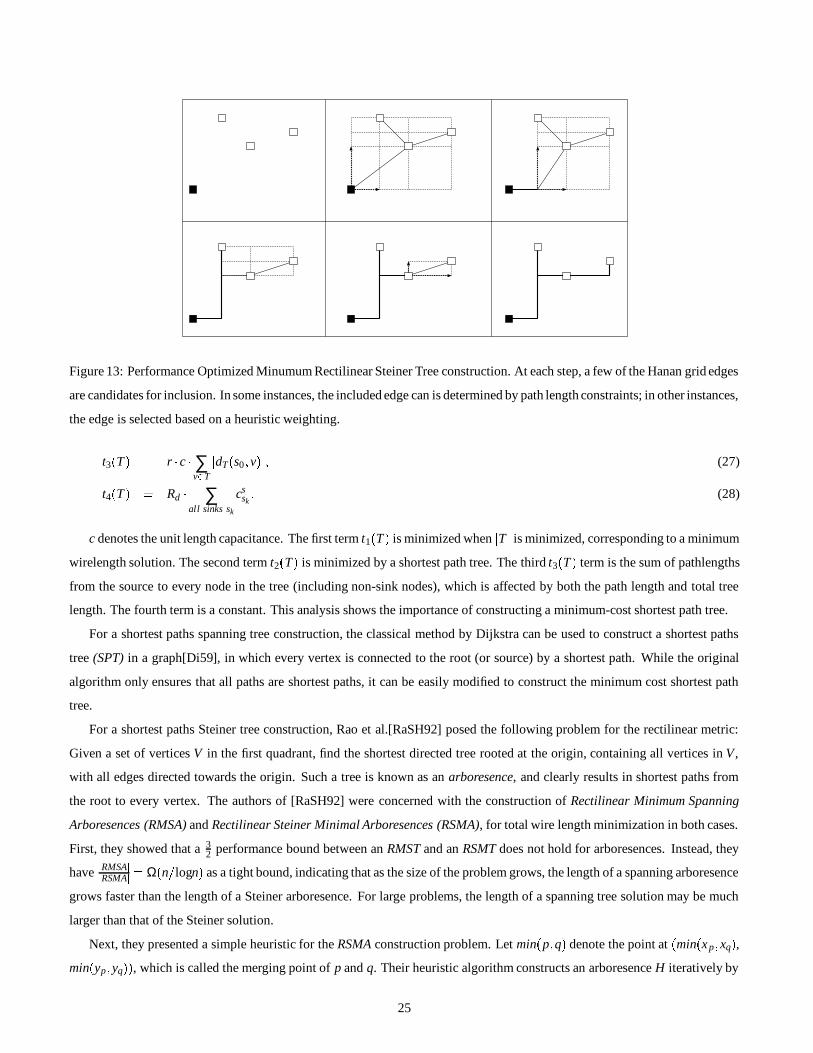
Figure 13: Performance Optimized Minumum Rectilinear Steiner Tree construction. At each step, a few of the Hanan grid edges
are candidates for inclusion. In some instances, the included edge can is determined by path length constraints; in other instances,
the edge is selected based on a heuristic weighting.
t3 T r c ∑v
T
dT s0 v (27)
t4 T Rd ∑all sinks sk
cssk (28)
c denotes the unit length capacitance. The first term t1 T is minimized when T is minimized, corresponding to a minimum
wirelength solution. The second term t2 T is minimized by a shortest path tree. The third t3 T term is the sum of pathlengths
from the source to every node in the tree (including non-sink nodes), which is affected by both the path length and total tree
length. The fourth term is a constant. This analysis shows the importance of constructing a minimum-cost shortest path tree.
For a shortest paths spanning tree construction, the classical method by Dijkstra can be used to construct a shortest paths
tree (SPT) in a graph[Di59], in which every vertex is connected to the root (or source) by a shortest path. While the original
algorithm only ensures that all paths are shortest paths, it can be easily modified to construct the minimum cost shortest path
tree.
For a shortest paths Steiner tree construction, Rao et al.[RaSH92] posed the following problem for the rectilinear metric:
Given a set of vertices V in the first quadrant, find the shortest directed tree rooted at the origin, containing all vertices in V ,
with all edges directed towards the origin. Such a tree is known as an arboresence, and clearly results in shortest paths from
the root to every vertex. The authors of [RaSH92] were concerned with the construction of Rectilinear Minimum Spanning
Arboresences (RMSA) and Rectilinear Steiner Minimal Arboresences (RSMA), for total wire length minimization in both cases.
First, they showed that a 32 performance bound between an RMST and an RSMT does not hold for arboresences. Instead, they
haveRMSA
RSMA
Ω n logn as a tight bound, indicating that as the size of the problem grows, the length of a spanning arboresence
grows faster than the length of a Steiner arboresence. For large problems, the length of a spanning tree solution may be much
larger than that of the Steiner solution.
Next, they presented a simple heuristic for the RSMA construction problem. Let min p q denote the point at min x p xq ,min yp yq , which is called the merging point of p and q. Their heuristic algorithm constructs an arboresence H iteratively by
25
connecting a pair of vertices p and q to min p q . The pair p and q are chosen to maximize the distance between min p q and
the root, i.e., the pair with the merging point furthest from the root are selected first. An example of tree construction using this
heuristic is shown in Figure 14.
Initial problem
1 2
3 4 5
Figure 14: The H heuristic, applied to a single quadrant problem.
Despite its simplicity, the algorithm provides an interesting bound on total tree length: T 2 RSMA , i.e., the length of
a tree generated by the heuristic is no worse than twice the optimal Steiner arboresence length.
When the problem is not restricted to one quadrant, the heuristic can be applied in the following manner. If we assume the
root to be located at the origin, we can restrict the tree to contain the x-axis in the range from a to b, a 0 b. Similarly, we
can restrict the tree to the y-axis for values c 0 d. By considering the single quadrant solutions given various values of a,
b, c, and d, and then finding the best performing combination, their heuristic constructs a tree in O n3logn time.
In [CoLZ93], Cong, Leung, and Zhou also addressed the construction of rectilinear Steiner arboresences, and presented
the A-Tree algorithm. The A-tree algorithm constructs trees by starting with a forest of points (the source and all sinks), and
then iteratively merges subtrees until all components are connected. In addition to the merging operation used in [RaSH92],
the authors of [CoLZ93] identify three types of “safe moves” for optimal merging at each step. In other words, the safe merge
moves preserve the tree length optimality during the construction process; if only safe moves are applied, the resulting tree
will have optimal length. The A-Tree algorithm applies safe moves whenever possible. On average, it was shown that 94% of
merge moves were optimal, and the trees constructed by the A-Tree algorithm were within 4% of the optimal arboresence length.
In experiments on random nets under the 0 5µ CMOS IC technology, the A-Tree constructions produced delay improvements
approaching 20% over 1-Steiner [KaRo92] constructions.
3.2.3 Multiple Source Routing
The existence of multiple source nets, such as signal busses, complicates interconnect topologyconstruction, as a topologywhich
provides good performance for one source may perform poorly for another. An example of such an instance is shown in Fig-
ure 15. A method proposed by Cong and Madden[CoMa95] constructs interconnect topologies which limit the maximum path
length between any pair of pins to the diameter of the net, while using minimal total wire length. Their Minimum-Cost Minimum
26
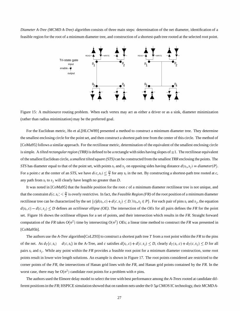
Diameter A-Tree (MCMD A-Tree) algorithm consists of three main steps: determination of the net diameter, identification of a
feasible region for the root of a minimum diameter tree, and construction of a shortest-path tree rooted at the selected root point.
WRITEREAD
p3
p1
p2
p4
WRITEREAD
p3
p1
p2
p4
Tri-state gateinput
output
enable
Figure 15: A multisource routing problem. When each vertex may act as either a driver or as a sink, diameter minimization
(rather than radius minimization) may be the preferred goal.
For the Euclidean metric, Ho et al.[HLCW89] presented a method to construct a minimum diameter tree. They determine
the smallest enclosing circle for the point set, and then construct a shortest path tree from the center of this circle. The method of
[CoMa95] follows a similar approach. For the rectilinear metric, determination of the equivalent of the smallest enclosing circle
is simple. A tilted rectangular region (TRR) is defined to be a rectangle with sides having slopes of
1. The rectilinear equivalent
of the smallest Euclidean circle, a smallest tiltedsquare (STS) can be constructed from the smallest TRR enclosing the points. The
STS has diameter equal to that of the point set, with points si and s j on opposing sides having distance d si s j diameter P .For a point c at the center of an STS, we have d c si D
2 for any si in the net. By constructing a shortest-path tree rooted at c,
any path from si to s j will clearly have length no greater than D.
It was noted in [CoMa95] that the feasible position for the root c of a minimum diameter rectilinear tree is not unique, and
that the constraint d c si D2 is overly restrictive. In fact, the Feasible Region (FR) of the root position of a minimum diameter
rectilinear tree can be characterized by the setc d si c d c s j D
si s j P . For each pair of pins si and s j, the equation
d si c d c s j D defines an octilinear ellipse (OE). The intersection of the OEs for all pairs defines the FR for the point
set. Figure 16 shows the octilinear ellipses for a set of points, and their intersection which results in the FR. Straight forward
computation of the FR takes O n2 time by intersecting O n2 OEs; a linear time method to construct the FR was presented in
[CoMa95b].
The authors use the A-Tree algorithm[CoLZ93] to construct a shortest path tree T from a root point within the FR to the pins
of the net. As dT c si d c si in the A-Tree, and c satisfies d si c d c s j D, clearly dT si c dT c s j D for all
pairs si and s j . While any point within the FR provides a feasible root point for a minimum diameter construction, some root
points result in lower wire length solutions. An example is shown in Figure 17. The root points considered are restricted to the
corner points of the FR, the intersections of Hanan grid lines with the FR, and Hanan grid points contained by the FR. In the
worst case, there may be O n2 candidate root points for a problem with n pins.
The authors used the Elmore delay model to select the tree with best performance among the A-Trees rooted at candidate dif-
ferent positions in the FR; HSPICE simulation showed that on random nets under the 0 5µ CMOS IC technology, their MCMD A-
27
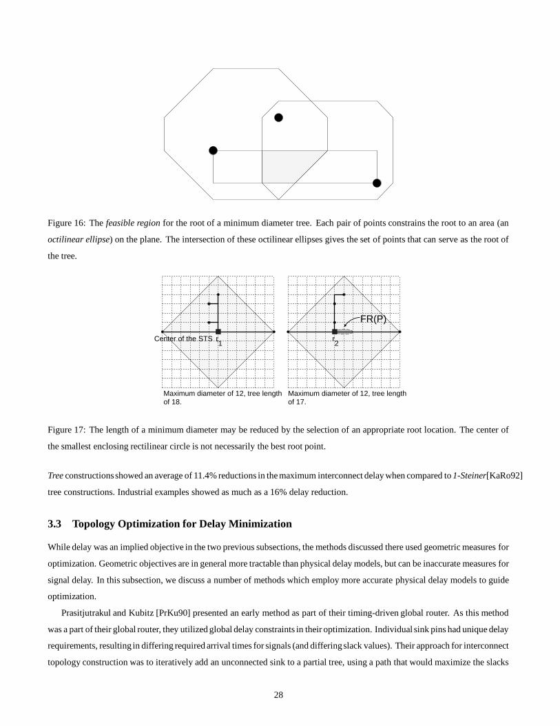
Figure 16: The feasible region for the root of a minimum diameter tree. Each pair of points constrains the root to an area (an
octilinear ellipse) on the plane. The intersection of these octilinear ellipses gives the set of points that can serve as the root of
the tree.
r r
Maximum diameter of 12, tree lengthof 18.
Maximum diameter of 12, tree lengthof 17.
Center of the , STS1 2
FR(P)
Figure 17: The length of a minimum diameter may be reduced by the selection of an appropriate root location. The center of
the smallest enclosing rectilinear circle is not necessarily the best root point.
Tree constructionsshowed an average of 11.4% reductions in the maximum interconnect delay when compared to 1-Steiner[KaRo92]
tree constructions. Industrial examples showed as much as a 16% delay reduction.
3.3 Topology Optimization for Delay Minimization
While delay was an implied objective in the two previous subsections, the methods discussed there used geometric measures for
optimization. Geometric objectives are in general more tractable than physical delay models, but can be inaccurate measures for
signal delay. In this subsection, we discuss a number of methods which employ more accurate physical delay models to guide
optimization.
Prasitjutrakul and Kubitz [PrKu90] presented an early method as part of their timing-driven global router. As this method
was a part of their global router, they utilized global delay constraints in their optimization. Individual sink pins had unique delay
requirements, resulting in differing required arrival times for signals (and differingslack values). Their approach for interconnect
topology construction was to iteratively add an unconnected sink to a partial tree, using a path that would maximize the slacks
28
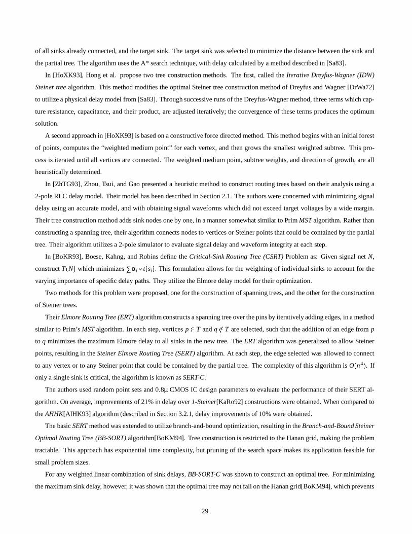
of all sinks already connected, and the target sink. The target sink was selected to minimize the distance between the sink and
the partial tree. The algorithm uses the A* search technique, with delay calculated by a method described in [Sa83].
In [HoXK93], Hong et al. propose two tree construction methods. The first, called the Iterative Dreyfus-Wagner (IDW)
Steiner tree algorithm. This method modifies the optimal Steiner tree construction method of Dreyfus and Wagner [DrWa72]
to utilize a physical delay model from [Sa83]. Through successive runs of the Dreyfus-Wagner method, three terms which cap-
ture resistance, capacitance, and their product, are adjusted iteratively; the convergence of these terms produces the optimum
solution.
A second approach in [HoXK93] is based on a constructive force directed method. This method begins with an initial forest
of points, computes the “weighted medium point” for each vertex, and then grows the smallest weighted subtree. This pro-
cess is iterated until all vertices are connected. The weighted medium point, subtree weights, and direction of growth, are all
heuristically determined.
In [ZhTG93], Zhou, Tsui, and Gao presented a heuristic method to construct routing trees based on their analysis using a
2-pole RLC delay model. Their model has been described in Section 2.1. The authors were concerned with minimizing signal
delay using an accurate model, and with obtaining signal waveforms which did not exceed target voltages by a wide margin.
Their tree construction method adds sink nodes one by one, in a manner somewhat similar to Prim MST algorithm. Rather than
constructing a spanning tree, their algorithm connects nodes to vertices or Steiner points that could be contained by the partial
tree. Their algorithm utilizes a 2-pole simulator to evaluate signal delay and waveform integrity at each step.
In [BoKR93], Boese, Kahng, and Robins define the Critical-Sink Routing Tree (CSRT) Problem as: Given signal net N,
construct T N which minimizes ∑αi t si This formulation allows for the weighting of individual sinks to account for the
varying importance of specific delay paths. They utilize the Elmore delay model for their optimization.
Two methods for this problem were proposed, one for the construction of spanning trees, and the other for the construction
of Steiner trees.
Their Elmore Routing Tree (ERT) algorithm constructs a spanning tree over the pins by iteratively adding edges, in a method
similar to Prim’s MST algorithm. In each step, vertices p T and q T are selected, such that the addition of an edge from p
to q minimizes the maximum Elmore delay to all sinks in the new tree. The ERT algorithm was generalized to allow Steiner
points, resulting in the Steiner Elmore Routing Tree (SERT) algorithm. At each step, the edge selected was allowed to connect
to any vertex or to any Steiner point that could be contained by the partial tree. The complexity of this algorithm is O n4 . If
only a single sink is critical, the algorithm is known as SERT-C.
The authors used random point sets and 0 8µ CMOS IC design parameters to evaluate the performance of their SERT al-
gorithm. On average, improvements of 21% in delay over 1-Steiner[KaRo92] constructions were obtained. When compared to
the AHHK[AlHK93] algorithm (described in Section 3.2.1, delay improvements of 10% were obtained.
The basic SERT method was extended to utilize branch-and-bound optimization, resulting in the Branch-and-Bound Steiner
Optimal Routing Tree (BB-SORT) algorithm[BoKM94]. Tree construction is restricted to the Hanan grid, making the problem
tractable. This approach has exponential time complexity, but pruning of the search space makes its application feasible for
small problem sizes.
For any weighted linear combination of sink delays, BB-SORT-C was shown to construct an optimal tree. For minimizing
the maximum sink delay, however, it was shown that the optimal tree may not fall on the Hanan grid[BoKM94], which prevents
29
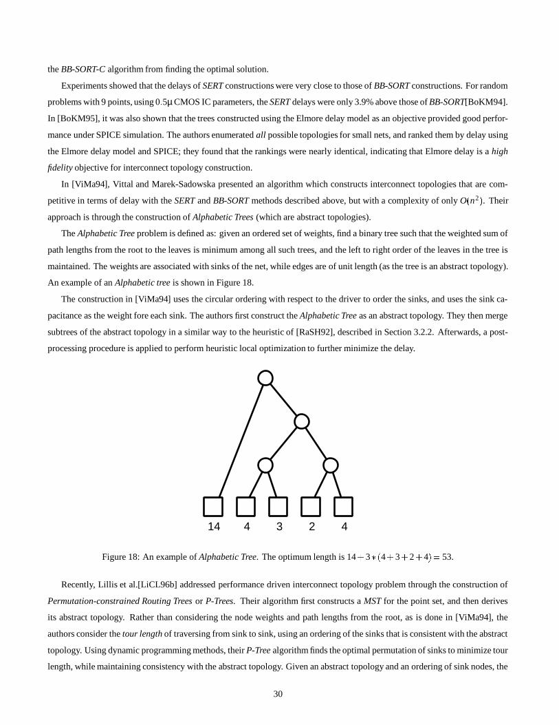
the BB-SORT-C algorithm from finding the optimal solution.
Experiments showed that the delays of SERT constructions were very close to those of BB-SORT constructions. For random
problems with 9 points, using 0 5µ CMOS IC parameters, the SERT delays were only 3.9% above those of BB-SORT[BoKM94].
In [BoKM95], it was also shown that the trees constructed using the Elmore delay model as an objective provided good perfor-
mance under SPICE simulation. The authors enumerated all possible topologies for small nets, and ranked them by delay using
the Elmore delay model and SPICE; they found that the rankings were nearly identical, indicating that Elmore delay is a high
fidelity objective for interconnect topology construction.
In [ViMa94], Vittal and Marek-Sadowska presented an algorithm which constructs interconnect topologies that are com-
petitive in terms of delay with the SERT and BB-SORT methods described above, but with a complexity of only O n2 . Their
approach is through the construction of Alphabetic Trees (which are abstract topologies).
The Alphabetic Tree problem is defined as: given an ordered set of weights, find a binary tree such that the weighted sum of
path lengths from the root to the leaves is minimum among all such trees, and the left to right order of the leaves in the tree is
maintained. The weights are associated with sinks of the net, while edges are of unit length (as the tree is an abstract topology).
An example of an Alphabetic tree is shown in Figure 18.
The construction in [ViMa94] uses the circular ordering with respect to the driver to order the sinks, and uses the sink ca-
pacitance as the weight fore each sink. The authors first construct the Alphabetic Tree as an abstract topology. They then merge
subtrees of the abstract topology in a similar way to the heuristic of [RaSH92], described in Section 3.2.2. Afterwards, a post-
processing procedure is applied to perform heuristic local optimization to further minimize the delay.
14 4 3 2 4
Figure 18: An example of Alphabetic Tree. The optimum length is 14 3 4 3 2 4 53.
Recently, Lillis et al.[LiCL96b] addressed performance driven interconnect topology problem through the construction of
Permutation-constrained Routing Trees or P-Trees. Their algorithm first constructs a MST for the point set, and then derives
its abstract topology. Rather than considering the node weights and path lengths from the root, as is done in [ViMa94], the
authors consider the tour length of traversing from sink to sink, using an ordering of the sinks that is consistent with the abstract
topology. Using dynamic programming methods, their P-Tree algorithm finds the optimal permutation of sinks to minimize tour
length, while maintaining consistency with the abstract topology. Given an abstract topology and an ordering of sink nodes, the
30

algorithm can then find the optimal embedding of the topology into the Hanan grid (through a dynamic programming approach
which considers possible locations for the internal nodes of the abstract topology). Solutions are chosen to optimize the Elmore
delay of the topology.
In all of the works mentioned earlier in this section, we have been interested in the construction of routing trees, and have
not allowed multiple connections between pairs of nodes.
Recent work, however, has considered the relative merits of non-tree routings. Xue and Kuh[XuKu95a, XuKu95b] have sug-
gested “multi-link insertion” as a method to reduce the resistance between a driver and critical sinks in a tree. In some respects,
this can be considered as a generalization on the variable wire width formulations which are detailed in a subsequent section. At
the heart of this approach is the observation that additional paths from a driver to a sink may substantially reduce the effective
interconnect resistance, with a nominal penalty to total interconnect length. Multiple paths between source and sink complicate
the delay analysis of an interconnect topology, and have higher interconnect length than tree constructions. At present, the use
of non-tree interconnect topologies is not wide spread.
4 Wire and Device Sizing
Both device sizing and interconnect sizing can be used to reduce the delay. A larger driver/gate at the source of an interconnect
tree has a stronger driving capability (or equivalently, smaller effective driver resistance), reducing the delay of this interconnect.
But a larger driver/gate also means a heavier load (larger sink capacitance) to the previous stage and thus increases its delay. The
device sizing problem is to determine the optimal size of each driver/gate to minimize the overall delay; this has been extensively
studied in the past. Interconnect sizing, often called wire-sizing, on the other hand, was investigated only recently. If the width of
a wire is increased, the resistance of the wire will go down, which may reduce the interconnect delay, but the capacitance of the
wire will go up, which may increase the interconnect delay. The wire-sizing problem is to determine the optimal wire width for
each wire segment to minimize the interconnect delay. When the interconnect resistance can be neglected as in the early days, the
interconnect can be modeled as a lumped capacitor. In this case, the minimum wire width is preferred for delay minimization and
only device sizing is necessary. But in the current deep submicron technology where the interconnect resistance can no longer be
neglected, both device and wire sizing are needed to reduce the interconnect delay. Techniques for both device and wire sizing
for delay minimization will be surveyed in this section. Sections 4.1 and 4.2 will present works on device sizing only and wire
sizing only, respectively. Section 4.3 will focus on simultaneous device and wire sizing works, and Section 4.4 on simultaneous
topology construction and sizing works. Because this survey deals mainly with interconnect design and optimization, more
emphasis will be given on wire-sizing and simultaneous device and wire sizing.
4.1 Device Sizing
The device sizing problem is equivalent to determining the transistor channel width in CMOS logic since the transistor channel
length is usually fixed to the minimum feature size. The following device sizing techniques are commonly used.
Driver sizing: A chain of cascaded drivers is usually used at the source of an interconnect tree for heavy capacitive load.
The driver sizing problem is to determine both the number of driver stages and the size for each driver.
31
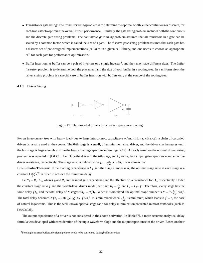
Transistor or gate sizing: The transistor sizing problem is to determine the optimal width, either continuous or discrete, for
each transistor to optimize the overall circuit performance. Similarly, the gate sizing problem includes both the continuous
and the discrete gate sizing problems. The continuous gate sizing problem assumes that all transistors in a gate can be
scaled by a common factor, which is called the size of a gate. The discrete gate sizing problem assumes that each gate has
a discrete set of pre-designed implementations (cells) as in a given cell library, and one needs to choose an appropriate
cell for each gate for performance optimization.
Buffer insertion: A buffer can be a pair of inverters or a single inverter4, and they may have different sizes. The buffer
insertion problem is to determine both the placement and the size of each buffer in a routing tree. In a uniform view, the
driver sizing problem is a special case of buffer insertion with buffers only at the source of the routing tree.
4.1.1 Driver Sizing
D0 D1 Di Dn-1
CL
Figure 19: The cascaded drivers for a heavy capacitance loading.
For an interconnect tree with heavy load (due to large interconnect capacitance or/and sink capacitance), a chain of cascaded
drivers is usually used at the source. The 0-th stage is a small, often minimum size, driver, and the driver size increases until
the last stage is large enough to drive the heavy loading capacitance (see Figure 19). An early result on the optimal driver sizing
problem was reported in [LiLi75]. Let Di be the driver of the i-th stage, and Ci and Ri be its input gate capacitance and effective
driver resistance, respectively. The stage ratio is defined to be fi CiCi 1
i 0 , it was shown that
Lin-Linholm Theorem: If the loading capacitance is CL and the stage number is N, the optimal stage ratio at each stage is a
constant CLC0 1 N in order to achieve the minimum delay.
Let τ0 R0 C0, where C0 and R0 are the input gate capacitance and the effective driver resistance for D0, respectively. Under
the constant stage ratio f and the switch-level driver model, we have Ri R0f i and Ci C0 f i. Therefore, every stage has the
same delay f τ0, and the total delay of N stages is td N f τ0. When N is not fixed, the optimal stage number is N ln CLCg ln f .
The total delay becomes N f τ0 ln CL Cg τ0 f ln f . It is minimized when fln f is minimum, which leads to f e, the base
of natural logarithms. This is the well known optimal stage ratio for delay minimization presented in most textbooks (such as
[MeCo93]).
The output capacitance of a driver is not considered in the above derivation. In [HeJe87], a more accurate analytical delay
formula was developed with consideration of the input waveform slope and the output capacitance of the driver. Based on their
4For single-inverter buffers, the signal polarity needs to be considered during buffer insertion
32

delay formula, the optimal stage ratio f satisfies
f e α f f
where α is the ratio between the intrinsic output capacitance and the input gate capacitance of the inverter. Since typical α is
about 1.35 for the technology they used, the optimal stage ratio is in the range of 3–5 instead of e. It is easy to find that the
optimal stage ratio is still e if α 0. The stage number N can be determined by the optimal stage ratio f as N ln CLC0
ln f .
Then, f is used for all stages, except that the last stage has a little bit larger ratio for delay minimization [HeJe87].
Most recently, Zhou and Liu [ZhLi96] discussed the optimal driver sizing for high-speed low-power ICs. The increasing
stage ratios fi f0 1 γ i are used, where γ is a modification factor determined by the I-V curve of the transistor. The typical
value of γ is around 0.2. The reason for the increasing stage ratio is the following: if the step waveform is applied at the input
of the very first stage, the waveforms become increasingly “softer” at the subsequent stages, i.e., the input waveform to the
following stage is no longer a step so an increasingly larger delay is expected for each following stage. Thus, an increasing
stage ratio is applied to maintain equal delay in different stages. The authors derived an analytic relationship between signal
delay, power dissipation, driver size and interconnect loading. They show that
f0 eγ2
2γ CLC0 1
and fi f0 1 γ i
are the optimal stage ratios for delay minimization. We would like to point out that all studies in [LiLi75, HeJe87, ZhLi96] also
discussed the optimal driver sizing for power minimization. Another study on optimal driver sizing for low-power can be found
in [Ve84].
4.1.2 Transistor and Gate Sizing
In addition to sizing drivers which usually drive global interconnects, the sizes of all transistors and gates in the entire circuit
or a sub-circuit can also be adjusted properly according to their capacitive loads for performance or power optimization. The
transistor sizing problem has been approached using both sensitivity based methods and mathematical optimization based meth-
ods. The gate sizing problem has been classified into both continuous and discrete gate sizing problems, and solved by different
approaches.
A. Sensitivity Based Transistor Sizing
Fishburn and Dunlop [FiDu85] studied the transistor sizing problems for synchronous MOS circuits. Let x1 xi xn be the
transistor sizes, A the total active area of transistors and T the clock period. If K is a positive constant, there are three forms for
the transistor sizing problem as follows:
1. Minimize A subject to the constraint T K.
2. Minimize T subject to the constraint A K.
3. Minimize ATK .
33
Let a transistor be modeled by the switch level model, then the gate, source and drain capacitance are all proportional to the
transistor size, and the effective resistance is inversely proportional to it. A CMOS gate will be modeled by a distributed RC
network. The Elmore delay (Eqn. (3)) is used to compute the worst-case delay of the gate, which is the delay through the highest
resistive path in the RC network. The delay of a PI-PO path is the sum of delays through all gates in the path. It is not difficult
to verify that the delay of a PI-PO path can be written into this form
∑1 i j N
ai jxi
x j ∑
1 i N
bi
xi(29)
where the ai j and bi are nonnegative constants. In fact, ai j is non-zero only when transistors i and j are dc-connected.
Furthermore, the authors of [FiDu85] show that Eqn. (29) and the area A ∑xi are posynomials and the transistor sizing
problems of the three forms are all posynomial programs.5 Even though posynomial programming methods can be used to
optimally solve the three forms of the transistor sizing problem, it is computationally expensive to be used for an entire circuit.
Thus the transistor sizing tool TILOS (TImed LOgic Synthesizer) was developed to minimize A subject to T K based on the
following scheme: First, the minimal size is assigned to all transistors. Then, timing analysis is performed to find the critical
delay T . If T is larger than K, the sensitivities of all transistors related to the critical path will be computed. The sensitivity is
defined as the delay reduction due to per transistor size increment. The size of the transistor with the largest sensitivity will be
multiplied by a user defined factor (BUMPSIZE) and then the algorithm goes to the timing analysis again. This procedure will
be terminated when the timing specification is satisfied or there is no improvement in the current loop, i.e., all sensitivities are
zero or negative. The performance of TILOS is quite good. Circuits with up to 40,000 transistors have been tested. Based on
the experiments, the results are reasonably close to the optimum under their delay model. However, it assumes that the effective
resistance for a transistor is independent of the waveform slope of the input. But, in fact, the input slope has a significant effect
on the transistor effective resistance. Another sensitivity based transistor sizing work is [Sap90] which also performs iterative
transistor sizing to reduce the critical path delay. In contrast to TILOS, it changes the size of more than one transistor in each
iteration. In addition, a sensitivity-based transistor sizing is presented by Borah et al. [BoOI95] to minimize power consumption
of CMOS circuit under delay constraint.
5According to [Ec80], a posynomial is a function of positive vector X Rm having the form g X ∑Ni 1 ui X with
ui X cixai11 xai2
2 xaimm i 1 2 N
where the exponents ai j are real numbers and the coefficients ci are positive. A posynomial program is the following minimization problem:
min g0 X sub ject to gk X 1
k 1 2 p and X 0
where each gk (k 0 1 2 p) is a posynomial. The posynomial program has the important property that the local optimum is also the global optimum. In
fact, the concepts of posynomial and posynomial program play an important role in many wire and device sizing works to be presented.
34
B. Mathematical Programming Based Transistor Sizing
Note that the method in [FiDu85] does not guarantee the optimality of the result. Studies have been done to formulate the tran-
sistor sizing problem as mathematical programming problems to obtain an optimal solution. Methods in [Ci87, He87, Ma86]
formulate the transistor sizing problem as nonlinear programs and solve them by the method of Lagrangian multipliers. Methods
in [DaAs89, HeFi91, ChKa91] apply the following two-step iterations. First, the delay budget is distributed to each gate; Then,
the transistors in each gate are sized optimally to satisfy the time budget.
Later, a two-phase algorithm was presented in [ShFD88] to minimize the circuit area under timing constraints: first, TILOS
[FiDu85] is used to generate an initial solution; then, a mathematic optimization is formulated and solved by using feasible
directions to find the optimal solution. The variables in the optimization problem, however, are not sizes of all transistors in the
circuit, but only sizes of those transistors that have been tuned by TILOS, thus it is still possible to lose the optimal solution with
respect to the whole circuit. Experimental results of circuits with up to 500 transistors have been presented.
More recently, Sapatnekar [SaRV93] developed a transistor sizing tool iCONTRAST, again, to minimize the circuit area
under timing constraints. It employs the analytical delay model developed in [HeJe87] which can consider the waveform slope
of input signals to transistors, but assumes that the transition time is twice the Elmore delay of the previous stage. Under the
delay model, the transistor sizing problem is a posynomial program that can be transformed into a convex program and the
convex programming method [Va89] was implemented to solve the transformed problem. When using the simple delay model
of TILOS [FiDu85], and the timing specification is loose, the area of the solution obtained by TILOS is close to that of the
solution obtained by the iCONTRAST algorithm. However, as the time specification is tightened, the TILOS-solutions have
larger area when compared with the iCONTRAST-solutions. Experimental results of circuits with up to 800 transistors have
been presented.
C. Continuous Gate Sizing
The continuous gate sizing problem assumes that all transistors in a gate can be scaled by a common factor, which is called the
size of a gate. In essence, it is very similar to the transistor sizing problem, but has much lower complexity for a given design,
since all transistors in a gate are scaled by the same factor. Hoppe et al [HoNS90] developed analytical models for signal delay,
chip area and dynamic power dissipation and formulated a nonlinear problem to minimize the weighted linear combination of
delay, area and power. The nonlinear problem is solved by the Newton-Raphson algorithm. A 64K-SRAM was optimized on a
mainframe computer in 2 hours.
In order to speed up the gate sizing problem, the linear programming (LP) formulation has been proposed. Berkelaar and Jess
[BeJe90] used a piecewise-linear (PWL) function to linearize the delay function. More precisely, one divides the gate sizes into
subranges so that the delay of a gate is a linear function of gate sizes within each subrange. Thus, the gate sizing problem can be
formulated as a LP problem. Their LP formulation [BeJe90] is to minimize the power subject to a delay constraint. Experimental
results on circuits with up to 500 gates were presented. Later on, their LP-based method was expanded [BeBJ94] to compute the
entire area or power-consumption versus delay trade-off curve. Results on MCNC’91 two-level benchmarks with up to 4,700
gates were reported. Recently, Tamiya, Matsunaga and Fujita [TaMF94] proposed another LP-based method where the latest and
the earliest arrival times are introduced so that the setup and hold time constraints can be handled. The objective is to minimize
35
the weighted linear combination of clock period, area and power. Result on a chip of 13,000 transistors was reported. Note that
gate sizing works in [BeJe90, BeBJ94, TaMF94] assume that the gate delay is a convex function of gate sizes, which is needed
to make sure that the error introduced by the PWL approximation is small. However, the gate delay in fact is not a strict convex
function.
More recently, Chen, Onodera and Tamaru [ChOT95] removed the convex delay model assumption in previous LP-based
works. They also divided the the gate sizes into subranges, but different from the previous works [BeBJ94, BeJe90, TaMF94]
where only one LP problem is formulated over the whole gate size range with the delay being a PWL function in this LP formu-
lation, a LP problem is formulated for every subrange with the delay being a linear function for each LP formulation. When the
subrange is small enough, the error introduced by the non-convexity will be small. The linear programming is performed itera-
tively, and subranges of gate sizes are updated according to the result from the previous step. Experimental results for ISCAS85
benchmarks with up to 3,500 gates were reported.
D. Discrete Gate Sizing
The resulting optimized design by the continuous gate sizing formulation may be impractical or expensive to implement since a
large number of manually-designed cells or a smart cell generator are needed. Thus, the discrete gate sizing problem is studied
by assuming that each gate has a discrete set of pre-designed implementations (cells) as in a given cell library and one needs
to choose an appropriate cell for each gate for performance optimization. In general, the discrete gate sizing problem is NP-
complete: Chan [Ch90] showed that the double sized discrete gate sizing problem to find discrete gate sizes to satisfy both
maximum and minimum delay constraints is NP-complete, even without consideration of area minimization. Hinsberger and
Kolla [HiKo92] proved the single-sided (with only maximum delay constraint) discrete gate sizing problem in a DAG (directed
acyclic graph) is NP-complete under three objectives: to minimize the maximum delay, to minimize the maximum delay under
an area constraint, and to minimize the area under a maximum delay constraint. Li [Li94] further showed that the discrete gate
sizing problem under both area and maximum delay constraints is strongly NP-hard even for a chain of gates.
The methods which are optimal for logic networks of certain structures have been proposed. For the double-sided problem, a
branch and bound algorithm [Ch90] was developed to find the optimal solution for tree structures. For the single-sided problem,
an optimal dynamic programming method to minimize the maximum delay was proposed, again for tree structures [HiKo92].
It assumes that the delay for a gate could be determined locally, i.e., the delay could be determined only by the sizes of the gate
and its fanout gates, and works in a bottom-up manner. Furthermore, an exact algorithm to minimize area subject to a maximum
delay constraint (single-sided) was presented for series-parallel circuits [LiLA92]. A simple series circuit is solved by a dynamic
programming method and a simple parallel circuit is solved by a number of transformations. All series-parallel circuits can be
solved recursively.
Heuristics have been proposed to expand the optimal algorithms for trees or series-parallel circuits to the general cases in
[Ch90, LiLA92]. Furthermore, the following methods have been developed: Lin, Marek-Sadowska and Kuh [LiMK90] use the
weighted sum of sensitivity and criticality to choose cell sizes for standard-cell designs. The sensitivity of a cell is defined as
∆delay∆area , where both delay and area are in terms of the cell. The criticality is inversely proportional to the slack of a cell so
36
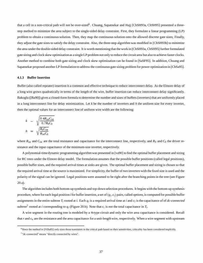
that a cell in a non-critical path will not be over-sized6 . Chuang, Sapatnekar and Hajj [ChSH93a, ChSH95] presented a three-
step method to minimize the area subject to the single-sided delay constraint. First, they formulate a linear programming (LP)
problem to obtain a continuous solution. Then, they map the continuous solution onto the allowed discrete gate sizes; Finally,
they adjust the gate sizes to satisfy the delay constraint. Also, the three-step algorithm was modified in [ChSH93b] to minimize
the area under the double-sided delay constraint. It is worth mentioning that the work in [ChSH93a, ChSH95] further formulated
gate sizing and clock skew optimizationas a single LP problem not only to reduce the circuit area but also to achieve faster clocks.
Another method to combine both gate sizing and clock skew optimization can be found in [SaSF95]. In addition, Chuang and
Sapatnekar proposed another LP formulation to address the continuous gate sizing problem for power optimization in [ChSa95].
4.1.3 Buffer Insertion
Buffer (also called repeater) insertion is a common and effective technique to reduce interconnect delay. As the Elmore delay of
a long wire grows quadratically in terms of the length of the wire, buffer insertion can reduce interconnect delay significantly.
Bakoglu ([Ba90]) gives a closed-form formula to determine the number and sizes of buffers (inverters) that are uniformly placed
in a long interconnect line for delay minimization. Let k be the number of inverters and h the uniform size for every inverter,
then the optimal values for an interconnect line of uniform wire width are the following:
k
0 4RintCint
0 7R0C0
h R0Cint
RintC0
where Rint and Cint are the total resistance and capacitance for the interconnect line, respectively, and R0 and C0 the driver re-
sistance and the input capacitance of the minimum-size inverter, respectively.
A polynomial-time dynamic programming algorithm was presented in [va90] to find the optimal buffer placement and sizing
for RC trees under the Elmore delay model. The formulation assumes that the possible buffer positions (called legal positions),
possible buffer sizes, and the required arrival times at sinks are given. The optimal buffer placement and sizing is chosen so that
the required arrival time at the source is maximized. For simplicity, the buffer of two inverters with the fixed size is used and the
polarity of the signal can be ignored. Legal positions were assumed to be right after the branching points in the tree (see Figure
20.a).
The algorithm includes both bottom-up synthesis and top-down selection procedures. It begins with the bottom-up synthesis
procedure, where for each legal position i for buffer insertion, a set of qi ci pairs, called options, is computed for possible buffer
assignments in the entire subtree Ti rooted at i. Each qi is a required arrival time at i and ci is the capacitance of of dc-connected
subtree7 rooted at i corresponding to qi (Figure 20.b). Note that ci is not the total capacitance in Ti.
A wire segment in the routing tree is modeled by a π-type circuit and only the wire area capacitance is considered. Recall
that r and ca are the resistance and the area capacitance for a unit-length wire, respectively. When a wire segment with upstream
6Since the method in [FiDu85] only sizes those transistors in the critical path based on their sensitivities, criticality has been considered implicitly.
7“dc-connected” means “directly connected by wires”.
37

iqi
b
ci T
Sink
(b)
b b
Tl Tr
(a)
i
Figure 20: (a) Legal position for buffer insertion; (b) An option in a legal position.
node k is added at i, an option qk ck will be generated at k for every qi ci at i as the following:
qk qi r l c l2 ci
ck ci c l
where l is the length of the wire segment.
A buffer is modeled by the input gate capacitance Cbu f , the driver resistance Rbu f and the intrinsic delay Dbu f . When a buffer
with input node k is inserted at i, an option will be generated at k for every qi ci at i as the following:
qk qi Dbu f Rbu f ci
ck Cbu f
When two subtrees Ti and Tj are merged at node k, for every pair of qi ci and q j c j (at i and j, respectively) an option
qk ck will be generated at k as the following:
qk min qi q j ck ci c j
The following pruning rule is used to prune a suboptimal option during the computation of options. For two options q c and q c in the same legal position, if c c and q q then q c is suboptimal, thus, it can be pruned from the solution
space. If the total number of legal positions is N, it was shown in [va90] that the total number of options at the source of the
whole routing tree is no larger than N 1 even though the number of possible buffer assignments is 2N .
After the bottom-upsynthesis procedure, the optimal option is the one which has the maximum requirement time at the source
pin of the whole interconnect tree. Then, the top-down selection procedure is carried out to trace back the buffer placement (in
general, also the buffer sizes) which led to the optimal option. Several extensions can be made. It is easy to allow buffers of
different types (sizes) to be placed. With different Rbu f Cbu f and Dbu f values for each type of buffer, there may be an extra option
generated in every legal position for every extra buffer type. Let B be the number of buffer types and N, again, be the total number
of legal positions, the total number of options at the root of the whole tree is bounded from above by N B. In general, the time
38
complexity of the algorithm is O N B 2 k , where N is the total number of legal positions for buffer insertion, B the total
number of buffer types and k the total number of sinks.
4.2 Wiresizing Optimization
It was first shown by Cong, Leung, and Zhou [CoLZ93] that when wire resistance becomes significant, as in the deep submi-
cron CMOS design, proper wire-sizing can further reduce the interconnect delay. Their work presented an optimal wire-sizing
algorithm for a single-source RC interconnect tree to minimize the uniform upper bound of the delay (Section 2.1, Eqn. (1)).
Later on, single-source wire-sizing algorithms were presented in [CoLe93, CoLe95, Sa94, XuKu95b, ChCW96b, ChCW96a]
using the Elmore delay model, in [MePD94] using a higher-order RC delay model and in [XuKY96] using a lossy transmission
line model. In addition, the wire-sizing problem for multiple-source nets was formulated and solved in [CoHe95]. Furthermore,
wire-sizing was carried out simultaneously with device sizing in [CoKo94, MePP95, MeBP95, LiCL95, CoHe96b, CoHe96c].
We classify the wire-sizing works according to their objective functions and present them in Sections 4.2.1 and 4.2.2, and then
discuss the simultaneous device and wire sizing in Section 4.3.
4.2.1 Wiresizing to Minimize Weighted Delay
In order to reduce the delays to multiple critical sinks in an interconnect tree with a single source, the wire-sizing algorithms
given by Cong and Leung [CoLe93, CoLe95] minimize a weighted combination of Elmore delays from the single source to
multiple critical sinks. Later on, Cong and He [CoHe95, CoHe96a] extended this formulation to the multiple-source net case,
where the objective is to minimize the weighted combination of Elmore delays between multiple source-sink pairs. Wiresizing
works in [CoLe93, CoLe95, CoHe95, CoHe96a] assumed that the wire widths are discrete and uniform within a wire segment or
sub-segment. Most recently in [ChCW96b], an optimal wire-sizing formula was derived by Chen et al. to achieve the continuous
and non-uniform wire width for each wire segment, again to minimize the weighted combination of Elmore delays from a single
source to a set of critical sinks. All these works assume that the weights of the delay penalty between the source and each sink
or each source-sink pair are given a prior.
A. Discrete Wiresizing for Single-Source RC Tree
In [CoLZ93], Cong, Leung and Zhou modeled an interconnect tree as a distributed RC tree and applied the upper-bound delay
model shown in Eqn. (1). They showed that when the driver resistance is much larger than the wire resistance of the interconnect,
the interconnect can be modeled as a lumped capacitor without losing much accuracy and that the conventional minimum wire
width solution often leads to an optimal design. However, when the resistance ratio, i.e. the driver resistance versus unit wire
resistance, is small, optimal wire-sizing can lead to substantial delay reduction. In addition, they developed the first polynomial-
time optimal wire-sizing algorithm. Since the uniform upper bound delay model does not distinguish the delays at different sinks
and may lead to over-sizing, Cong and Leung [CoLe93, CoLe95] extended the work to the Elmore delay formulation of Eqn.
(3). Their formulation and method are summarized as follows.
Given a routing tree T , let sink T denote the set of sinks in T , W be the wire-sizing solution (i.e., wire width assignment
for each segment of T) and ti W be the Elmore delay from the source to sink si under W . The following weighted combination
39
of delays is used as the objective function for wire-sizing optimization.
t W ∑si
sink T λi ti W (30)
where λi is the weight of the delay penalty to sink si. The larger λi, the more critical sink si is.
The following monotone property and separability were shown in [CoLe95].
Monotone Property: Given a routing tree, there exists an optimal wire-sizing solution W such that we we if segment
e Ans e .
Separability: Given the wire width assignment of a path P originated from the source, the optimal wire width assignment
for each subtree branching off from P can be carried out independently.
Based on these two properties, the optimal wire-sizing algorithm (OWSA) was developed. It is a dynamic programming
method based on the wire-sizing solution for a single-stem tree, which is a tree with only one segment (called the stem segment
of that tree) incident on its root (see Figure 21(a)). We use sst e to denote the single-stem tree with stem e.
According to the separability, once e and every ancestor segment of e are assigned the appropriate widths, the optimal wire
width assignment for the single-stem subtrees sst ec1 , sst ec2 , sst ecb of the tree sst e (with respect to the width assign-
ment of e and its ancestors) can be independently determined, where the segments ec1 ecb are the children of e. Therefore,
given a set of possible widthsW1 W2 Wr , OWSA enumerates all the possible width assignments of e. For each possible
width assignment Wk of e (1 k r), the optimal wire-sizing is determined for each single-stem subtree sst eci (1 i b)
of sst e independently by recursively applying the same procedure to each sst eci withW1 W2 Wk as the set of possible
widths (to guarantee the monotone property). The optimal assignment for e is the one which gives the smallest total delay.
If the original routing tree T is not a single-stem tree, we can decompose it into b single-stem trees, where b is the degree
of the root of T , and apply the algorithm to each individual single-stem tree separately (see Figure 21(b)). The worst-case time
complexity of OWSA is O nr , which is much faster than brute-force enumeration O rn , where n is the number of wire segments
and r is the number of possible wire widths. However, OWSA algorithm can be slow when r is large.
In order to further speed-up the OWSA algorithm, the greedy wire-sizing algorithm (GWSA) was developed based on the
local refinement and the dominance property to compute the lower and upper bounds of the optimal wire widths.
Given two wire-sizing solutions W and W , W is defined to dominate W if we w e for every segment e. Given a wire-
sizing solution W for the routing tree, and any particular segment e in the tree, a local refinement on e is defined to be the
operation to optimize the width of e while keeping the wire width assignment of W on other segments unchanged. The following
dominance property was shown in [CoLe95]
Dominance Property: Suppose that W
is an optimal wire-sizing solution. If a wire-sizing solution W dominates W,
then any local refinement of W still dominates W. Similarly, if W is dominated by W
, then any local refinement of W is
still dominated by W.
The GWSA algorithm works as follows: starting with the minimum-width assignment, GWSA traverses the tree and per-
forms a local refinement on each segment whenever possible. This process is repeated until no improvement is achieved on
any segment in the last round of traversal. According to the dominance property, a lower bound of the optimal wire width on
every segment is obtained. An upper bound of the optimal wire width assignment can be obtained similarly by starting with the
40
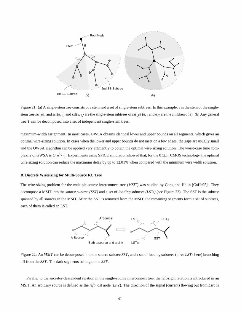
(b)(a)
Stem
1st SS-Subtree
2nd SS-Subtree
Root Node
E
Ec1Ec2
Figure 21: (a) A single-stem tree consists of a stem and a set of single-stem subtrees. In this example, e is the stem of the single-
stem tree sst e , and sst ec1 and sst ec2 are the single-stem subtrees of sst e (ec1 and ec2 are the children of e). (b) Any general
tree T can be decomposed into a set of independent single-stem trees.
maximum-width assignment. In most cases, GWSA obtains identical lower and upper bounds on all segments, which gives an
optimal wire-sizing solution. In cases when the lower and upper bounds do not meet on a few edges, the gaps are usually small
and the OWSA algorithm can be applied very efficiently to obtain the optimal wire-sizing solution. The worst-case time com-
plexity of GWSA is O n3 r . Experiments using SPICE simulation showed that, for the 0 5µm CMOS technology, the optimal
wire sizing solution can reduce the maximum delay by up to 12.01% when compared with the minimum wire width solution.
B. Discrete Wiresizing for Multi-Source RC Tree
The wire-sizing problem for the multiple-source interconnect tree (MSIT) was studied by Cong and He in [CoHe95]. They
decompose a MSIT into the source subtree (SST) and a set of loading subtrees (LSTs) (see Figure 22). The SST is the subtree
spanned by all sources in the MSIT. After the SST is removed from the MSIT, the remaining segments form a set of subtrees,
each of them is called an LST.
SSTA Source
Both a source and a sink
A Source LST2
LST3
LST1
Figure 22: An MSIT can be decomposed into the source subtree SST, and a set of loading subtrees (three LSTs here) branching
off from the SST . The dark segments belong to the SST .
Parallel to the ancestor-descendent relation in the single-source interconnect tree, the left-right relation is introduced in an
MSIT. An arbitrary source is defined as the leftmost node (Lsrc). The direction of the signal (current) flowing out from Lsrc is
41

the right direction along each segment. Under such definitions, the signal in any LST always flows rightward, but the signal
may flow either leftward or rightward in the SST.
The following properties were shown in [CoHe95] for the wire-sizing problem for MSITs (the MSWS problem):
LST Separability: Given the wire width assignment of the SST, the optimal width assignment for each LST branching off
from the SST can be carried out independently. Furthermore, given the wire width assignment of both the SST and a path P
originated from the root of an LST, the optimal wire width assignment for each subtree branching off from P can be carried out
independently.
LST Monotone Property: For an MSIT, there exists an optimal wire-sizing solution W
where the wire widths decrease
monotonically rightward within each LST in the MSIT.
Because of the two properties, the polynomial-time OWSA algorithm developed for single-source wire-sizing in [CoLe95]
can be applied to compute the optimal wire widths independently for each LST when given the wire width assignments for the
SST. Furthermore, the authors of [CoHe95] proved that the MSWS problem has the dominance property presented in Section
4.2.1.A. Thus, the GWSA algorithm, again developed in [CoLe95] for the single-source wire-sizing problem, can be applied to
compute the lower and upper bounds for the optimal solution of the MSWS problem. When the lower and upper bounds do not
meet for all segments, the authors propose to enumerate the wire width assignment for the SST between the lower and upper
bounds. During each enumeration of the SST, OWSA is applied independently for each LST to compute an optimal wire-sizing
solution between the lower and upper bounds. Because the identical lower and upper bounds are often obtained by the GWSA
algorithm for all segments, the optimal wire-sizing solution can be achieved very efficiently in practice. Experiments using
SPICE simulations showed that the optimal wire-sizing solution reduces the maximum delay by up to 36.9% (for an MSIT from
the industry with the total wire length of 31980µm) when compared with the minimum wire width solution in the 0 5µm CMOS
technology.
C. Discrete Wiresizing Using Variable Segment-Division
An assumption is made for wire-sizing algorithms presented in Subsections 4.2.1.A and 4.2.1.B that the wire width does not
change within a segment. Intuitively, better wire-sizing solutions may be achieved when variable wire width is allowed within a
segment. In [CoKo94], a segment is further divided into a sequence of grid-edges with a unit length and the wire width is allowed
to change every grid-edge. The fine and uniform segment-division, however, may result in high memory usage and computation
time. An approach based on the bundled refinement property was proposed by Cong and He [CoHe95] to decide the appropriate
segment-division during the wire-sizing procedure. It uses much less memory and computation time and is applicable to both
single-source and multi-source wire-sizing problems. For the simplicity of presentation, we assume the multi-source wire-sizing
problem since the single-source wire-sizing problem is a simple case of it.
First, the concepts of uni-segment and min-segment were introduced. Each segment is divided intoa sequence of uni-segments
and each uni-segment has a uniform wire width within it. The wire-sizing problem is formulated to find an optimal wire width
for every uni-segment. A min-segment is a uni-segment of the minimum length, which is set by the user or determined by the
technology. The finest segment-division is the one with each uni-segment being a min-segment.
Then, the following property was revealed in [CoHe95], even though the signal direction in the SST of an MSIT may be
changed with respect to different sources.
42
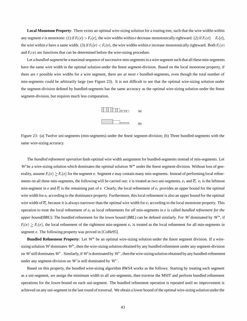
Local Monotone Property: There exists an optimal wire-sizing solution for a routing tree, such that the wire widths within
any segment e is monotone: (1) if Fl e Fr e , the wire widths within e decrease monotonically rightward. (2) if Fl e Fr e ,the wire within e have a same width. (3) if Fl e Fr e , the wire widths within e increase monotonically rightward. Both Fl e and Fr e are functions that can be determined before the wire-sizing procedure.
Let a bundled-segmentbe a maximal sequence of successive min-segments in a wire segment such that all these min-segments
have the same wire width in the optimal solution under the finest segment-division. Based on the local monotone property, if
there are r possible wire widths for a wire segment, there are at most r bundled-segments, even though the total number of
min-segments could be arbitrarily large (see Figure 23). It is not difficult to see that the optimal wire-sizing solution under
the segment-division defined by bundled-segments has the same accuracy as the optimal wire-sizing solution under the finest
segment-division, but requires much less computation.
(b)
(a)
Figure 23: (a) Twelve uni-segments (min-segments) under the finest segment-division; (b) Three bundled-segments with the
same wire-sizing accuracy.
The bundled refinement operation finds optimal wire width assignment for bundled-segments instead of min-segments. Let
W be a wire-sizing solution which dominates the optimal solution W
under the finest segment-division. Without loss of gen-
erality, assume Fl e Fr e for the segment e. Segment e may contain many min-segments. Instead of performing local refine-
ments on all these min-segments, the following will be carried out: e is treated as two uni-segments, e l and el . el is the leftmost
min-segment in e and el is the remaining part of e. Clearly, the local refinement of el provides an upper bound for the optimal
wire width for el according to the dominance property. Furthermore, this local refinement is also an upper bound for the optimal
wire width of el , because it is always narrower than the optimal wire width for el according to the local monotone property. This
operation to treat the local refinement of el as local refinements for all min-segments in e is called bundled refinement for the
upper bound(BRU). The bundled refinement for the lower bound (BRL) can be defined similarly. For W dominated by W, if
Fl e Fr e , the local refinement of the rightmost min-segment er is treated as the local refinement for all min-segments in
segment e. The following property was proved in [CoHe95].
Bundled Refinement Property: Let W
be an optimal wire-sizing solution under the finest segment division. If a wire-
sizing solution W dominates W, then the wire-sizing solution obtained by any bundled refinement under any segment-division
on W still dominates W. Similarly, if W is dominated by W
, then the wire-sizingsolutionobtained by any bundled-refinement
under any segment-division on W is still dominated by W.
Based on this property, the bundled wire-sizing algorithm BWSA works as the follows: Starting by treating each segment
as a uni-segment, we assign the minimum width to all uni-segments, then traverse the MSIT and perform bundled refinement
operations for the lower-bound on each uni-segment. The bundled refinement operation is repeated until no improvement is
achieved on any uni-segment in the last round of traversal. We obtain a lower bound of the optimal wire-sizing solution under the
43

finest segment-division. Similarly, we assign the maximum width to all uni-segments and perform bundled refinement operations
for the upper-bound, and obtain an upper bound of the optimal wire-sizing solution. This is the first pass of the BWSA algorithm.
After each pass, one checks the lower and upper bounds. If there is a gap between the lower and upper bounds for a uni-
segment, it is non-convergent. For every non-convergent uni-segment longer than a min-segment, it will be divided into two
uni-segments of equal length and each inherits the lower and upper bounds of their parent. Then, another pass to compute the
lower/upper bounds is carried out by performing bundled refinement operations under the refined segment-division.
The BWSA algorithm iterates through a number of passes until either identical lower and upper bounds are achieved for
all uni-segments or each non-convergent uni-segment is a min-segment. It was shown in [CoHe95] that the lower and upper
bound obtained by the BWSA algorithm under the iteratively refined segment-division is as tight as those obtained by the GWSA
algorithm under the finest segment-division where every uni-segment is a min-segment. Both algorithms have the same worst-
case complexity, however, experiments showed that the BWSA algorithm often runs 100x time faster than the GWSA algorithm
under the finest segment-division. In addition to replacing the GWSA algorithm in both the single-source and multi-source wire-
sizing problems, the BWSA algorithm can be used in the simultaneous driver and wire sizing problem [CoKo94] to be presented
in Section 4.3.1.
D. Continuous and Non-uniform Wiresizing for Single-Source RC Tree
Another alternative to achieve non-uniformwire width withina segment is the optimal wire-sizing formula proposed in [ChCW96b]
very recently. Let f x be the wire width at positionx of a wire segment. When given the driver resistance and the loading capac-
itance for the wire segment, Chen et al. show that the Elmore delay through the wire segment is minimized when f x ae bx
where a and b are constants. Furthermore, when the lower and upper bounds for the wire width of a wire segment are given,
the optimal wire width function is one of the six truncated forms of ae bx. In all cases, formulas can be determined in constant
time. However, it did not model the fringing capacitance.
In order to apply the optimal wire-sizing formula to a routing tree, the authors propose to minimize the weighted combination
of Elmore delays from the source to multiple sinks. A procedure like the GWSA algorithm developed in [CoLe95] is used. First,
the minimum wire width is assigned to every segment. Then, the optimal wire-sizing formula is iteratively applied to each wire
segment until no improvement can be achieved. In contrast to the case of a single wire segment, the total upstream weighted
resistance is used to replace the driver resistance, and the total downstream capacitance to replace the loading capacitance. The
resulting wire width is continuous and non-uniform within a wire segment. Note that when a discrete wire-sizing solution is
needed, the mapping from a continuous solution to a discrete solution may lose its optimality.
4.2.2 Wiresizing to Minimize Maximum Delay or Achieve Target Delay
In addition to minimizing the weighted combination of delays, wire-sizing methods have been developed to minimize the max-
imum delay or achieve a target delay. We will present first the wire-sizing work [Sa94] to minimize the maximum delay in
Subsection 4.2.2.A, where the Elmore delay model is used, then the wire-sizing work [MePD94] to achieve the target delay in
Subsection 4.2.2.B, where a higher-order RC delay model is used, and finally the wire-sizing work [XuKY96] to minimize the
maximum delay for a tree of transmission lines in Subsection 4.2.2.C, where a lossy transmission line model is used. Note that
the Elmore delay model is suitable for formulations that minimize the weighted sum of delays for current CMOS designs, since
44

it has high fidelity with respect to the SPICE-computed delay for the wire-sizing optimization, which is verified by the exper-
iments in [CoHe96a] based on the 0.5 µm CMOS designs. On the other hand, in order to achieve the target delay or handle
MCM designs, more accurate delay models are required as in [MePD94, XuKY96]. Furthermore, several iterations of the pro-
cedures to minimize the weighted delay can be used to minimize the maximum delay or achieve the target delay by adjusting
the weight penalty assignment in practice. Particularly, the Lagrangian relaxation wire-sizing work [ChCW96a] proposes an
optimal method to assign the weight penalty, which will be presented in Subsection 4.2.2.D.
A. Single-Source RC Tree under Elmore Delay Model
Sapatnekar [Sa94] studied the wire-sizing problem to minimize the maximum delay under the Elmore delay formulation of Eqn.
(3). First, he showed that the separability no longer holds for minimizing the maximum delay. So, the dynamic programming
based approach in [CoLZ93, CoLe93] does not apply. However, since the Elmore delay in an RC tree is a posynomial function
of wire widths as first pointed out in [FiDu85], it has this property that the local optimum is also the global optimum; thus a
sensitivity-based method like that used in [FiDu85] can be applied.
The algorithm in [Sa94] goes through a number of iterations. In each iteration, the sink with the largest delay is identified
and the sensitivity Si given in the following is computed for each wire segment i on the path from the source to the identified
sink:
Si Delay F wi Delay wi F 1 wi
where Delay wi is the delay from the source to the identified sink and F is a constant larger than 1 (set to 1.2 or 1.5 in [Sa94]).
Intuitively, the sensitivity is the delay reduction of unit wire area increment. For all wires on the path from the source to the
identified sink, the width of the wire with the minimum negative sensitivity will be multiplied by F 1. The iteration is stopped
when no wire has a negative sensitivity or the delay specification is satisfied.
Since a posynomial function can be mapped into a convex function, the convex programming technique developed in [Va89,
SaRV93] was applied in [SaSa94] by Sancheti and Sapatnekar to achieve the exact solution at higher computation costs. Note
that both algorithms in [Sa94] and [SaSa94] produce wire-sizing solutions assuming continuous wire width choices, and then
map them into the discrete wire widths. The optimality of the wire-sizing solution may be lost after mapping.
B. Single-Source RC Tree under Higher-Order RC Delay Model
In [MePD94], a moment fitting approach is used to wiresize RC interconnect trees to achieve the target delays and slopes at
critical sinks. Let target moments be moments for the 2-pole transfer functions that have the target delays and slopes at critical
sinks, and real moments those for the transfer function under the current wire width assignment for the RC tree, Menezes et al.
propose to modify the wire width assignment in the RC tree to match the real moments with the target moments so that the target
delays and slopes will be obtained.
The sensitivities of real moments with respect to the wire widths are used to guide the search for the proper wire widths. The
method works as follows: First, for each sink, a 2-pole transfer function is generated so that it has the target delay and slope at the
sink. For each transfer function, the first four target moments are obtained. Then, the first four real moments are computed for
45
each sink based on the recursive method developed in [PiRo90], which computes the higher moments from the lower moments,
and a O MN2 method is proposed to compute the sensitivities with respect to the wire widths for real moments, where M is the
number of critical sinks and N the number of wire segments. Finally, such sensitivity values guide the search for wire widths to
minimize the mean square error between the first four target moments and the first four real moments for every critical sink.
Furthermore, the following is proposed in order to achieve the solution with smaller area: each wire is assigned a weight
in order to favor those wires which are related to the more critical sinks and those wires with respect to which the critical sinks
exhibit larger Elmore delay sensitivities. Widening those wires has the maximum effect on delay with a minimal area penalty.
Moreover, the delay sensitivity with respect to the driver area is also computed and compared with the delay sensitivity with
respect to the interconnect area to empirically determine whether a larger driver should be used. The approach is extended in
[MePP95] to conduct simultaneous gate and interconnect sizing, which will be presented in Section 4.3. Note that the algorithm
in [MePD94], similar to [Sa94, SaSa94], assumes continuous wire width choices for their wire-sizing solutions.
C. Single-Source Tree of Transmission Lines under Lossy Transmission Line Model
The wire-sizing work by Xue and Kuh in [XuKY96] takes the wire inductance into account by modeling each wire segment as a
lossy transmission line, and sizes the wire segments in an interconnect tree to minimize the maximum delay. The maximum delay
and its sensitivities with respect to wire widths are computed via high order moments. Based on the exact moment matching
method in [YuKu95a], the higher moments and their sensitivities with respect to the wire widths are computed recursively from
the lower moments and the sensitivities can be computed analytically. Thus, the maximum delay and its sensitivities with respect
to the wire widths can be computed efficiently. The following procedure is repeated to reduce the maximum delay: First, one
computes the high order moments, the maximum delay (td) and its sensitivity with respect to every wire width ( ∂td∂wi
). Then, if a
wire segment ei has the maximum ∂td∂wi
, ei will be assigned either the next larger or smaller wire width, based on the polarity
of ∂td∂wi
. The procedure iterates until the sensitivities of the maximum delay becomes small.
[XuKY96] showed the following experimental results: The 2-pole transfer function with moments m0 m1 and m2 m0 0 is reasonably accurate when compared with SPICE2. The approach can reduce the rising delay in the critical sink by over 60%
with a small penalty in routing area 8 . The monotone property is still true under this lossy transmission line formulation. The
final wire-sizing solution reduces the overshoot and is more robust under parameter variation.
D. Weighted Delay Formulation versus Maximum Delay Formulation
All the wire-sizing algorithms presented in Section 4.2.1 for minimizing the weighted sum of delays can be used to minimize
the maximum delay by iteratively adjusting the weights so that the sinks with larger delays have higher weights. In particular,
Chen, Chang and Wong [ChCW96a] showed that for the continuous wire-sizing formulation where the wire width can be any
value between the lower and upper bounds, the weighted delay formulation is able to optimally minimize the maximum delay
8Note that the delay in a tree of transmission lines is the sum of flying time and the rising delay of the response waveform. Wiresizing only affects the rising
delay, and the delay reduction means the reduction of the maximum rising delay at threshold voltage of 0.5Vdd
46

among all sinks. They formulated the following Lagrangian relaxation problem:
Minimize tmax ∑si
sink T λi ti W tmax
Sub ject to ti W tmax
where ti W is the delay from the source to sink si under the current wire-sizing solution W and tmax is the maximum delay
from the source to all sinks.
The following two-level algorithm was proposed in [ChCW96a]: in the outer loop, the weights associated with the delays
from the source to sinks are dynamically adjusted, which are basically proportional to the delays at the sinks. In the inner loop,
the continuous wire-sizing solution is computed for the given set of weights, by the wire-sizing algorithm [ChCW96b] (Sec-
tion 4.2.1.D) to minimize the weighted linear combination of delays. They showed that the Lagrangian relaxation iteration will
converge to an optimal solution in terms of maximum-delay minimization. Moreover, the authors expanded their Lagrangian
relaxation based algorithm to simultaneous wire and buffer sizing for buffered clock trees to minimize the weighted combination
of delay, power and area minimization, and to address the problem of skew and sensitivity minimization for clock trees.
4.3 Simultaneous Device and Wire Sizing
The device sizing works presented in Section 4.1 model the interconnect as a lumped loading capacitor and do not consider the
possibilityof sizing the interconnect. On the other hand, the wiresizing works presented in Section 4.2 model the driver as a fixed
effective resistor and do not consider the need to size the device again after interconnects have been changed. Both approaches
may lead to suboptimal designs. As a result, a number of recent studies size both devices and interconnects simultaneously.
These methods will be discussed in this subsection.
4.3.1 Simultaneous Driver and Wire Sizing
The simultaneous driver and wire sizing problem for delay minimization (SDWS/D problem) was studied in [CoKo94]. The
switch-level model is used for a driver and both the gate and the drain (output) capacitances of the transistor are taken into
account, while the interconnect tree is modeled by a distributed RC tree as was used in [CoLe95]. The objective function is to
minimize the summation of the delay for cascaded drivers and the weighted delay for the RC tree. The SDWS/D algorithm is
based on the following important relation between the driver size and the optimal wire sizing:
Driver and Wire Sizing Relation [CoKo94]: Let Rd be the effective resistance for the last stage driver and W
be the
optimal wire sizing solution for driver resistance Rd . If Rd is reduced to R d , the new corresponding optimal wiresizing solution
W dominates W
.
The core for the SDWS/D algorithm is the procedure to compute the optimal driver and wire sizing when given a stage num-
ber k, which works as follows. First, the algorithm starts with the minimum wire width assignment and computes the capacitive
load of the routing tree. Then, it computes the optimal sizes of the k cascaded drivers based on Lin-Linholm Theorem in Sec-
tion 4.1.1. Next, the optimal wiresizing algorithms (GWSA followed by OWSA) developed in [CoLe95] are performed on the
routing tree based on the effective resistance of the last driver. If the wire width assignment changes, the new driver sizes are
obtained according to Lin-Linholm Theorem. Then, the optimal wiresizing solution will be computed again based on the new
47
size of the last driver. The process is repeated until the wire width assignments do not change in consecutive iterations. In this
case, the lower bounds are obtained for the optimal sizes of both the drivers and the wire segments.
The upper bound for the optimal sizing solution can be obtained similarly by beginning with the maximum wire width as-
signments. If the lower and upper bounds meet, the optimal solution is achieved, which occurs in almost all cases as shown in
the paper. Otherwise, the size of the last driver is enumerated between the lower and upper bounds. The corresponding optimal
wire sizes and the first k 1 driver sizes are computed, and the optimal k-driver SDWS/D solution is selected for this set.
The overall SDWS/D algorithm computes the optimal number of stages by a linear search, increasing k starting with k 1.
The process terminates when stage k does not perform better than stage k 1 (i.e. when adding an additional driver actually
slows down the circuit). Then, the optimal sizing solution for the k 1 stage drivers and the corresponding optimal wiresiz-
ing is the optimal SDWS/D solution. In practice, the runtime of SDWS/D is on the same order as k times the runtime of the
GWSA algorithm followed by the OWSA algorithm to compute the optimal wiresizing algorithm. Note that the BWSA algo-
rithm [CoHe95] presented in Section 4.2.1.C can be used to greatly speed-up the computation of the optimal wiresizing solution.
The simultaneous driver and wire sizing problem for power minimization was also studied in [CoKo94] and the efficient optimal
algorithm was developed. Accurate SPICE simulation shows that the method reduces the delay by up to 12%–49% and power
dissipation by 26%–63% compared with existing design methods. Very recently, Cong, Koh, and Leung [CoKL96] extended
the work on SDWS to handle driver/buffer and wire sizing for buffered interconnects. However, both [CoKo94, CoKL96] do
not consider the waveform slope effect during the computation of the optimal driver/buffer sizes.
4.3.2 Simultaneous Gate and Wire Sizing
Recently, Menezes et al. [MePP95, MeBP95] studied the simultaneous gate and wire sizing problem for different objectives: to
achieve the target delays in [MePP95], and to find the minimal-area solution to satisfy the performance requirement in [MeBP95].
A. Simultaneous Gate and Wire Sizing to Achieve Target Delay
The algorithm in [MePP95] is the extension of the moment fitting method for wiresizing [MePD94] (Section 4.2.2.C) to the
simultaneous gate and wire sizing problem. Again, let target moments be moments for the 2-pole transfer functions that has the
target delays, and real moments those for the transfer function under the current widths of all wires and gates, the sensitivities
of the real moments with respect to the wire and gate widths will guide the search for wire and gate widths to match the real
moments and target moments.
A higher-order RC delay model is used for the interconnect tree as in [MePD94]. Meanwhile, all transistors in a gate are
assumed to scale by the same factor, which allows that a gate can be described by its “width” wg. The gate is modeled by the
single-resistor voltage-ramp model as proposed in [DaMQ94] (see Figure 6), which can accurately estimate the driver delay as
well as output waveform slope. The sensitives with respect to the gate and wire widths for real moments can be computed, which
are used to guide the changes of gate and wire widths to achieve the target delay for a stage by the aforementioned moment-fitting
method (in this work, a stage is a dc-connected path from the voltage source in the gate model to a sink).
Furthermore, the algorithm in [MePP95] handles a path, which contains cascaded stages. It is also based on the sensitivity
guided moment-fitting method. The following assumption is made to simplify the sensitivity computations: given two succes-
sive stages n and n 1 in a path, first, except the gate of stage n 1, no wire/gate in stages n 1 n 2 affects the delay in
48
stage n; Second, sizing the gate or a wire in stage n only affects the input transition time to the gate in stage n 1, not those in
stages n 1 n 2 . In their experiment, the objective for each PI-PO path was a 50% delay reduction, through gate sizing
only and simultaneous gate and wire sizing, respectively. It was shown that for larger delay reductions, simultaneous gate and
wire sizing could achieve lower area and that gate sizing only could not reach 50% delay reduction because the path delay was
dominated by the interconnect delay. The trade-off between the area and the delay reduction was shown as well.
B. Simultaneous Gate and Wire Sizing to Satisfy Performance Requirement
The simultaneous gate and wire sizing approach [MeBP95] is aimed at finding the minimal-area solution to satisfy the perfor-
mance requirement. First, the driver is modeled by a fixed resistance driven by a step waveform and the delay of the interconnect
tree is modeled by the Elmore delay model. The path delay in this case is a posynomial function of both gate and wire widths and
the simultaneous gate and wire sizing problem is a posynomial programming problem which can be transformed into a convex
programming problem. The sequential quadratic programming (SQP) 9 is used to solve this transformed convex programming
problem to achieve an optimal solution.
Then, the delay of the interconnect tree is modeled by the higher-order RC delay while the driver is modeled by a fixed
resistance. Although the path delay is no longer a posynomial function of gate and wire widths, the authors assumed that it was
near-posynomial so that the SQP method could be applied. A q-pole transfer function is used and the sensitivity computation of
the poles and residues is conducted during the SQP procedure.
Finally, the driver is modeled by the more accurate single-resistorvoltage-ramp model [DaMQ94]. Again, the near-posynomial
is assumed for path delay and the SQP method is applied. The sizing results showed that the fixed-resistance driver model could
lead to undersized solutions. RC meshes (non-tree interconnects) can be handled by the SQP method, again under the assumption
that the delay formulation is near-posynomial.
4.3.3 Simultaneous Transistor and Wire Sizing
Very recently, the simultaneous transistor and interconnect(wire) sizing (STIS) problem is formulated and solved by Cong and
He [CoHe96b, CoHe96c]. In order to minimize the delay along multiple PI-PO paths, they propose to minimize the weighted
combination of delays for all stages in these PI-PO paths by choosing the discrete or continuous transistor sizes and wire widths.
Rather than developing ad hoc methods for STIS problems under different delay models, the authors study the optimization
problems whose objective functions have the following form:
f X m
∑p 0
m
∑q 0
n
∑i 1
n
∑j 1 j
i
api xi xp
i bq j x j xq
j
where api xi 0 and bq j x j 0
0 L X U (31)
9According to [Po78], the SQP method reduces the nonlinear optimization to a sequence of quadratic programming (QP) subproblems. At each iteration,
a QP subproblem is constructed from a quadratic linearization of both the objective function and the constraints about the solution from the previous iteration.
The solution of the current iteration is then used as an initial solution for the next iteration. The iteration converges to a solution for a convex programming
problem.
49
When coefficients are constants, the class of functions, named simple CH-posynomials, is a subset of posynomials defined in
[Ec80]. Furthermore, they define the following general CH-posynomials, which are no longer posynomials.
General CH-posynomial: Eqn. (31) is a general CH-posynomial if coefficients satisfy the following conditions: (i) a pi xi is a function of xi. It monotonically increases with respect to an increase of xi but
api xi xp
istill monotonicallydecreases with respect
to an increase of xi. (ii) bq j x j is a function of x j . It monotonically decreases with respect to an increase of x j but bq j x j xqj
still monotonically increases with respect to an increase of xi.
Let the optimization problem to minimize a simple/general CH-posynomial be a simple/general CH-posynomial program.
After generalizing the concepts of local refinement operation and the dominance property in [CoLe95] (presented in Section
4.2.1.A), the authors of [CoHe96b, CoHe96c] showed the following important theorem:
Theorem (Cong-He): The dominance property holds for both the simple and the general CH-posynomial programs.
The theorem provides an easy way to verify the dominance property for both the single-source and the multi-source wiresiz-
ing problems in [CoLe95] and [CoHe95], respectively, since both objective functionsare instances of the simple CH-posynomial.
Furthermore, the theorem leads to efficient algorithms, for example, the generalizations of the GWSA algorithm [CoLe95] or the
BWSA algorithm [CoHe95], to compute a set of lower and upper bounds of the optimal solution to a CH-posynomial program
by the local refinement operation and the bundled refinement operation very efficiently (in polynomial time).
The authors of [CoHe96b, CoHe96c] further show that the STIS problem is a CH-posynomial program under the RC tree
model for interconnects and a number models for the transistors, including both simple analytical models or more accurate table-
lookup based models obtained by detailed simulation to consider the effect of the waveform slope. Thus, the BWSA algorithm
[CoHe95] is generalized to compute the lower and upper bounds for the optimal widths for both wires and transistors.
Experiments show that in nearly all cases, the optimal solution to the STIS problem is achieved because the recursive ap-
plication of local refinement operations using the dominance property leads to identical lower and upper bounds. In contrast
to the transistor sizing algorithm in [FiDu85] that is not able to consider the waveform-slope effect for transistors, the domi-
nance property based STIS algorithm can be efficiently applied to either analytical or table-lookup based transistor models with
consideration of the waveform-slope effect. The simultaneous driver and wire sizing problem (for multi-source nets) and the
simultaneous buffer and wire sizing problem have been solved as special cases of the STIS problem, and a smooth area-delay
trade-off has been yielded for the transistor sizing problem for circuits implemented by complex gates.
4.3.4 Simultaneous Buffer Insertion and Wire Sizing
The polynomial-time dynamic programming algorithm for the buffer insertion problem [va90] was generalized in [LiCL95] to
handle the simultaneous wiresizing and buffer insertion for both delay and power minimization. The slope effect on the buffer
delay was also taken into account. Only the delay minimization feature will be discussed in the following.
Different from [va90], when a wire segment of length l (with upstream node k) is added at the root i of a dc-connected subtree,
a new option qk ck will be generated at k for every wire width choice w and every qi ci at i as the following:
qk qi
rw l ca w l
2 ci
Ck ci ca w l
50

The non-uniform wiresizing can be easily carried out by just introducing 2-degree Steiner points within a wire segment, and
the other two bottom-up rules to compute new options (with extension to multiple inverter sizes and consideration of the signal
polarity) and the rule to prune suboptimal options given in [va90] can be applied without any modifications. The number of total
options at the source of the routing tree is still polynomial bounded.
According to [HeJe87], the delay of an inverter is the delay under the step input plus an increment due to the input slope. The
increment is proportional to the input waveform transition time. By assuming that the delay increment due to the input slope is
proportional to the Elmore delay Dprev in the previous stage, [LiCL95] further formulated the following buffer (inverter) delay
for the downstream capacitance ck .
bu f delays b ck bu f delay b ck λbDprev
where buf delay(b ck) equals to Dbu f Rbu f ck with Dbu f being the intrinsic delay of an inverter and Dprev being the Elmore
delay of the previous wire path.
Because the dynamic programming works from the bottom-upand Dprev is unknown, the option is re-defined as f c instead
of q c when considering the slope effect, where f is a piece-wise linear function and f x q is the optimal required arrival
time q for the downstream capacitance c and Dprev x. With this new definition for the option, the number of total options at
the source of a routing tree is no longer polynomially bounded in the theoretical sense. However, it was observed in [LiCL95]
that the run time of the new version is comparable to that of its simpler version assuming step-input to buffers.
4.4 Simultaneous Topology Construction and Sizing
All wire and device sizing works presented up to now assume that the topology of interconnects is given, which can be called
static sizing. Recently, dynamic wiresizing has been studied, where the wiresizing is performed during interconnect construc-
tion. Furthermore, simultaneous interconnect construction, buffer insertion and sizing, and wiresizing has been studied in order
to achieve even better designs.
4.4.1 Dynamic Wiresizing during Topology Construction
Hodes, McCoy and Robins [HoMR94] propose a method to do wiresizing dynamically during tree construction. They combine
the Elmore Routing Tree (ERT) algorithm [BoKR93] (Section 3.3) and the GWSA algorithm [CoLe93] (Section 4.2.1) as fol-
lows: starting with a degenerate tree initially consisting of only the source pin, grow the tree at each step by finding a new pin
to connect to the tree in order to minimize the Elmore delay in the current wiresized topology. In other words, in each step they
invoke the GWSA algorithm for each candidate edge and add the edge that yields the wiresized tree with the minimal maximum
delay. After the construction spans the entire net, the GWSA algorithm is invoked once more to wiresize the entire tree, starting
with the minimal width.
Recently, Xue and Kuh [XuKu95b, XuKu95a] propose insertion of multi-links into an existing routing tree and do dynamic
wiresizing during the link insertion in order to minimize the maximum delay. The Elmore delay formulation for RC meshes in
[Wy87] is used. The algorithm works as follows: Given a routing tree with a performance requirement, the sink nmax with the
maximum delay is identified. A wire link e is established between the source and nmax. While the performance requirement is
51
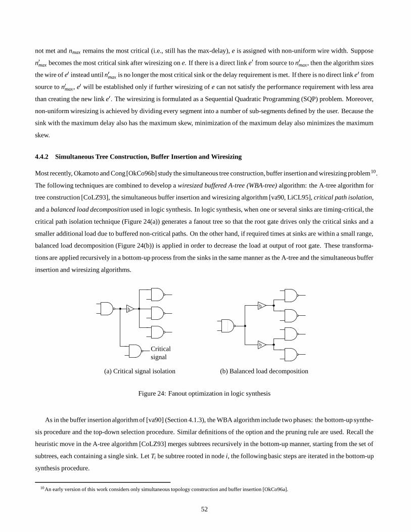
not met and nmax remains the most critical (i.e., still has the max-delay), e is assigned with non-uniform wire width. Suppose
n max becomes the most critical sink after wiresizing on e. If there is a direct link e from source to n max, then the algorithm sizes
the wire of e instead until n max is no longer the most critical sink or the delay requirement is met. If there is no direct link e from
source to n max, e will be established only if further wiresizing of e can not satisfy the performance requirement with less area
than creating the new link e . The wiresizing is formulated as a Sequential Quadratic Programming (SQP) problem. Moreover,
non-uniform wiresizing is achieved by dividing every segment into a number of sub-segments defined by the user. Because the
sink with the maximum delay also has the maximum skew, minimization of the maximum delay also minimizes the maximum
skew.
4.4.2 Simultaneous Tree Construction, Buffer Insertion and Wiresizing
Most recently, Okamoto and Cong[OkCo96b] study the simultaneous tree construction, buffer insertionand wiresizing problem10.
The following techniques are combined to develop a wiresized buffered A-tree (WBA-tree) algorithm: the A-tree algorithm for
tree construction [CoLZ93], the simultaneous buffer insertion and wiresizing algorithm [va90, LiCL95], critical path isolation,
and a balanced load decomposition used in logic synthesis. In logic synthesis, when one or several sinks are timing-critical, the
critical path isolation technique (Figure 24(a)) generates a fanout tree so that the root gate drives only the critical sinks and a
smaller additional load due to buffered non-critical paths. On the other hand, if required times at sinks are within a small range,
balanced load decomposition (Figure 24(b)) is applied in order to decrease the load at output of root gate. These transforma-
tions are applied recursively in a bottom-up process from the sinks in the same manner as the A-tree and the simultaneous buffer
insertion and wiresizing algorithms.
(a) Critical signal isolation
Criticalsignal
b
(b) Balanced load decomposition
b
b
Figure 24: Fanout optimization in logic synthesis
As in the buffer insertion algorithm of [va90] (Section 4.1.3), the WBA algorithm include two phases: the bottom-up synthe-
sis procedure and the top-down selection procedure. Similar definitions of the option and the pruning rule are used. Recall the
heuristic move in the A-tree algorithm [CoLZ93] merges subtrees recursively in the bottom-up manner, starting from the set of
subtrees, each containing a single sink. Let Ti be subtree rooted in node i, the following basic steps are iterated in the bottom-up
synthesis procedure.
10An early version of this work considers only simultaneous topology construction and buffer insertion [OkCo96a].
52

Select v and w with considering critical path isolation and balanced load decomposition.
Merge Tv and Tw to Tr, and compute a set of options at r.
In order to select the pair of v and w (equivalent to Tv and Tw) to merge, first, the following concepts are defined:
The distance between the source and the merging pair of v and w, denoted Dvw , is defined as Dvw min vx wx min vy wy .This definition is for the case that v and w are in the first quadrant with s0 at the origin. Other cases can be defined in a similar
way.
The maximum possible required time at the root r of subtree Tr generated by merging of Tv and Tw , denoted Rvw , is defined
as Rvw maxz
Zr qz, where r is the merging point of Tv and Tw, and Zr is a set of options at r.
The maximum Rvw among all possible merging pairs v and w in the set of roots ROOT of the current subtrees, denoted
Rmax ROOT , is defined as Rmax ROOT maxv w
ROOT Rvw
The merging cost for v and w is defined as merge cost v w ROOT α Rvw 1 α Dvw where α is a fixed constant
with 0 α 1 0.
Then, the v and w pair with the maximum merge cost is the one to be merged. The idea behind it is as follows: we want to
maximize the required arrival time in the source pin so that we wish that the Rvw is as large as possible. Meanwhile, we want
to minimize the total wire length, intuitively, we wish that Dvw is as large as possible. Note that, when α 0, it is equivalent to
the heuristic move in [CoLZ93].
The option computation and pruning can be carried out in a manner similar to [va90, LiCL95] after each merging of Tv and
Tw . Overall, after the bottom-up synthesis procedure to construct tree and compute options, the top-down selection procedure
is invoked. It chooses the option which gives the maximum required time and the minimum total capacitance at the source pin,
then traces back the computations in the first phase that led to this option. During the back-trace, the buffer positions and wire
width of each segments are determined.
Similarly, Lillis et al studied the simultaneous tree construction and wiresizing problem [LiCL96b] and the simultaneous
tree construction and buffer insertion problem [LiCL96a], respectively. In fact, their method can generalized to handle the si-
multaneous tree construction, buffer insertion and wiresizing problem as well. In short, during the dynamic program scheme to
construct a P-Tree [LiCL96b] (Section 3.3) in a bottom-up manner for a given permutation, a set of options are computed for
each subtree as in [va90, LiCL95] and the same option pruning rule is applied.
5 High-Performance Clock Routing
In layout synthesis, the distribution of clock signals is critical to both the operation and performance of synchronous systems.
If not properly controlled, the clock skew, defined to be the difference in the clock signal delays to registers, can impact the
performance of the system and even cause erratic operations of the system, e.g., latching of an incorrect data signal within a
register. At the same time, the routing solutions to distribute the clock signals should have low wiring area to reduce the die size
and the capacitive effects on both performance and power dissipation. Due to technology scaling where long global interconnect
becomes highly resistive as the wire dimensions decreases, the clock routing problem has become increasingly important since
clock nets generally have very large fanout and span the entire chip. Thus, clock synthesis has generated tremendous interests
53
within both the industrial and academic communities over the past several years.
In general, the clock routing problem can be formulated as follows: Given a setl s1 l sn R 2 of sink (register) lo-
cations and skew constraints on various pairs of registers, construct a minimum-cost clock tree that satisfies the skew constraints.
Most of the works deal with zero-skew clock tree (ZST) construction where all sinks are required to have identical clock delay.
There are possibly other constraints and/or objectives to the problem:
(i) We want to impose a constraint on the rise/fall times of the clock signal at the sinks since it is critical to keep the clock
signal waveform clean and sharp.
(ii) We want to minimize the delay of clock signal, which is closely related to the rise/fall time.
(iii) We want to minimize the total power dissipation since a clock signal typically operates at a very high frequency and
dissipates a large amount of the power.
(iv) We want the clock tree to be tolerant of process variations, which cause the wire widths and device sizes on the fabricated
chip to differ from the specified wire widths and device sizes, respectively, resulting in so-called process skew, i.e. clock skew
due to process variations.
In the rest of the discussion on clock routing, we consider the following clock routing problem: Given a set of sink locations
and a skew bound B 0, construct a minimum-cost clock tree T that satisfies skew T B where skew T max i j ti t j .In most works, B 0, i.e., they attempt to achieve zero-skew for the clock net. This formulation requires the clock signal to
arrive at all sequential elements almost at the same time, which is commonly used in random logic design. For data path design,
however, it is possible to optimize the circuit performance by planning the clock arrival times (clock schedule) at all registers
more carefully; “intentional” clock skews are used constructively to improve system performance. Clock schedule optimization
will be discussed in Section 5.6.
Recent works on clock skew minimization have accomplished exact zero skew under both the pathlengthdelay model [BoKa92,
Ed91, Ed92] and the Elmore delay model [Ts91, BoKa92, ChHH92a, ChHH92b]. The Deferred-Merge Embedding (DME) al-
gorithm by [BoKa92, ChHH92a, Ed91] can be either applied to a given clock topology or combined with a clock topology
generation algorithm to achieve zero skew with a smaller wirelength [Ed93a]. The methods in [CoKo95, HuKT95, CoKK95]
address the bounded-skew tree (BST) construction problem under the pathlength and Elmore delay models by extending the
DME algorithm for zero-skew tree to BST/DME algorithms by the enabling concept of a merging region, which generalizes the
merging segment concept of [BoKa92, ChHH92a, Ed91] for zero-skew clock trees. Recent studies on clock routing have also led
to new methods for single-layer (planar) clock routing [ZhDa92, KaTs94a, KaTs94b]. Furthermore, a number of authors have
applied wiresizing optimizations and/or buffer optimizations to minimize phase delay [PuMO93, Ed93b, MePP93, PuMP93],
skew sensitivity to process variation [PuMO93, ChCh94, LiWo94, XiDa95], and/or power dissipation [PuMO93, ViMa95].
Most of these works are based on the pathlength and Elmore delay models. In practice, bounding pathlength skew does not
provide reliable control of actual delay skew [CoKK95]. For example, Figure 25(a) plots HSPICE delay skew against path-
length delay skew for routing trees generated by the Greedy-BST/DME algorithm under pathlength delay [CoKo95, HuKT95]
on MCNC benchmark circuit r3 [Ts91]. Not only is the correlation poor, but the pathlength-based BST solutions simply cannot
meet tight skew bounds (of 100ps or less). On the other hand, Figure 25(b) demonstrates the accuracy and fidelity of Elmore
delay skew to actual skew for routing trees constructed by the Greedy-BST/DME algorithm under Elmore delay [CoKK95].
Nevertheless, for completeness, we will discuss studies under both pathlength and Elmore delay models. The clock routing
54
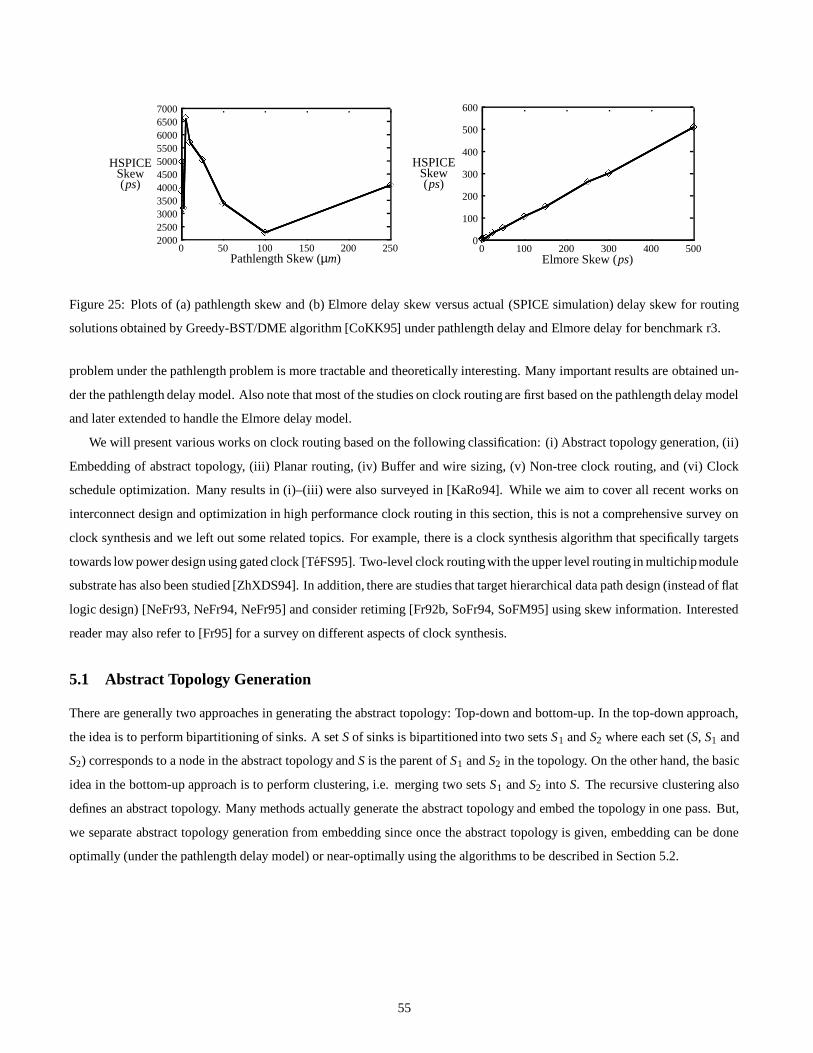
20002500300035004000450050005500600065007000
0 50 100 150 200 250
HSPICESkew(ps)
Pathlength Skew (µm)
0
100
200
300
400
500
600
0 100 200 300 400 500
HSPICESkew(ps)
Elmore Skew (ps)
Figure 25: Plots of (a) pathlength skew and (b) Elmore delay skew versus actual (SPICE simulation) delay skew for routing
solutions obtained by Greedy-BST/DME algorithm [CoKK95] under pathlength delay and Elmore delay for benchmark r3.
problem under the pathlength problem is more tractable and theoretically interesting. Many important results are obtained un-
der the pathlength delay model. Also note that most of the studies on clock routing are first based on the pathlength delay model
and later extended to handle the Elmore delay model.
We will present various works on clock routing based on the following classification: (i) Abstract topology generation, (ii)
Embedding of abstract topology, (iii) Planar routing, (iv) Buffer and wire sizing, (v) Non-tree clock routing, and (vi) Clock
schedule optimization. Many results in (i)–(iii) were also surveyed in [KaRo94]. While we aim to cover all recent works on
interconnect design and optimization in high performance clock routing in this section, this is not a comprehensive survey on
clock synthesis and we left out some related topics. For example, there is a clock synthesis algorithm that specifically targets
towards low power design using gated clock [TeFS95]. Two-level clock routingwith the upper level routing in multichipmodule
substrate has also been studied [ZhXDS94]. In addition, there are studies that target hierarchical data path design (instead of flat
logic design) [NeFr93, NeFr94, NeFr95] and consider retiming [Fr92b, SoFr94, SoFM95] using skew information. Interested
reader may also refer to [Fr95] for a survey on different aspects of clock synthesis.
5.1 Abstract Topology Generation
There are generally two approaches in generating the abstract topology: Top-down and bottom-up. In the top-down approach,
the idea is to perform bipartitioning of sinks. A set S of sinks is bipartitioned into two sets S1 and S2 where each set (S, S1 and
S2) corresponds to a node in the abstract topology and S is the parent of S1 and S2 in the topology. On the other hand, the basic
idea in the bottom-up approach is to perform clustering, i.e. merging two sets S1 and S2 into S. The recursive clustering also
defines an abstract topology. Many methods actually generate the abstract topology and embed the topology in one pass. But,
we separate abstract topology generation from embedding since once the abstract topology is given, embedding can be done
optimally (under the pathlength delay model) or near-optimally using the algorithms to be described in Section 5.2.
55
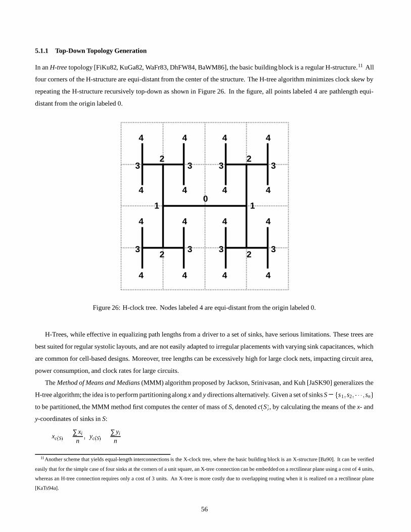
5.1.1 Top-Down Topology Generation
In an H-tree topology [FiKu82, KuGa82, WaFr83, DhFW84, BaWM86], the basic building block is a regular H-structure.11 All
four corners of the H-structure are equi-distant from the center of the structure. The H-tree algorithm minimizes clock skew by
repeating the H-structure recursively top-down as shown in Figure 26. In the figure, all points labeled 4 are pathlength equi-
distant from the origin labeled 0.
01 1
2
2 2
2
3333
4444
4444
4444
4444
3333
Figure 26: H-clock tree. Nodes labeled 4 are equi-distant from the origin labeled 0.
H-Trees, while effective in equalizing path lengths from a driver to a set of sinks, have serious limitations. These trees are
best suited for regular systolic layouts, and are not easily adapted to irregular placements with varying sink capacitances, which
are common for cell-based designs. Moreover, tree lengths can be excessively high for large clock nets, impacting circuit area,
power consumption, and clock rates for large circuits.
The Method of Means and Medians (MMM) algorithm proposed by Jackson, Srinivasan, and Kuh [JaSK90] generalizes the
H-tree algorithm; the idea is to perform partitioningalong x and y directions alternatively. Given a set of sinks S s1 s2 sn
to be partitioned, the MMM method first computes the center of mass of S, denoted c S , by calculating the means of the x- and
y-coordinates of sinks in S:
xc S ∑xi
n yc S ∑yi
n
11Another scheme that yields equal-length interconnections is the X-clock tree, where the basic building block is an X-structure [Ba90]. It can be verified
easily that for the simple case of four sinks at the corners of a unit square, an X-tree connection can be embedded on a rectilinear plane using a cost of 4 units,
whereas an H-tree connection requires only a cost of 3 units. An X-tree is more costly due to overlapping routing when it is realized on a rectilinear plane
[KaTs94a].
56
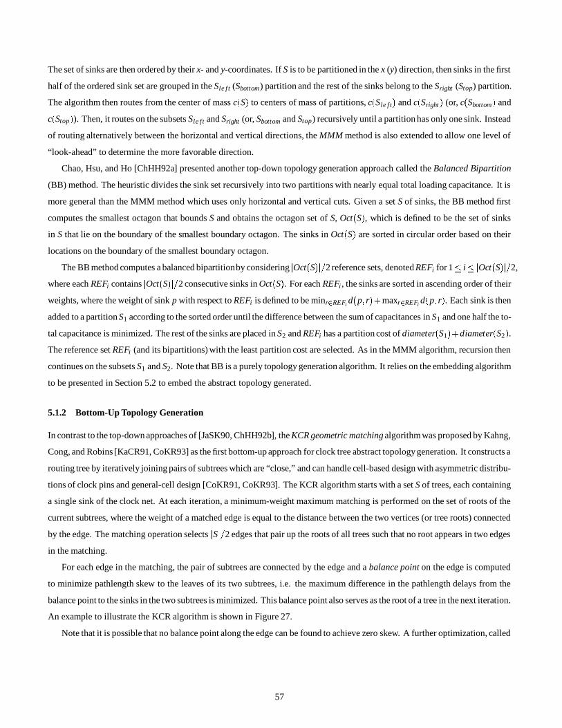
The set of sinks are then ordered by their x- and y-coordinates. If S is to be partitioned in the x (y) direction, then sinks in the first
half of the ordered sink set are grouped in the Sle f t (Sbottom) partition and the rest of the sinks belong to the Sright (Stop) partition.
The algorithm then routes from the center of mass c S to centers of mass of partitions, c Sle f t and c Sright (or, c Sbottom and
c Stop ). Then, it routes on the subsets Sle f t and Sright (or, Sbottom and Stop) recursively until a partition has only one sink. Instead
of routing alternatively between the horizontal and vertical directions, the MMM method is also extended to allow one level of
“look-ahead” to determine the more favorable direction.
Chao, Hsu, and Ho [ChHH92a] presented another top-down topology generation approach called the Balanced Bipartition
(BB) method. The heuristic divides the sink set recursively into two partitions with nearly equal total loading capacitance. It is
more general than the MMM method which uses only horizontal and vertical cuts. Given a set S of sinks, the BB method first
computes the smallest octagon that bounds S and obtains the octagon set of S, Oct S , which is defined to be the set of sinks
in S that lie on the boundary of the smallest boundary octagon. The sinks in Oct S are sorted in circular order based on their
locations on the boundary of the smallest boundary octagon.
The BB method computes a balanced bipartitionby considering Oct S 2 reference sets, denoted REFi for 1 i Oct S 2,
where each REFi contains Oct S 2 consecutive sinks in Oct S . For each REFi , the sinks are sorted in ascending order of their
weights, where the weight of sink p with respect to REFi is defined to be minr
REFid p r maxr
REFi
d p r . Each sink is then
added to a partition S1 according to the sorted order until the difference between the sum of capacitances in S1 and one half the to-
tal capacitance is minimized. The rest of the sinks are placed in S2 and REFi has a partition cost of diameter S1 diameter S2 .The reference set REFi (and its bipartitions) with the least partition cost are selected. As in the MMM algorithm, recursion then
continues on the subsets S1 and S2. Note that BB is a purely topology generation algorithm. It relies on the embedding algorithm
to be presented in Section 5.2 to embed the abstract topology generated.
5.1.2 Bottom-Up Topology Generation
In contrast to the top-down approaches of [JaSK90, ChHH92b], the KCR geometric matching algorithm was proposed by Kahng,
Cong, and Robins [KaCR91, CoKR93] as the first bottom-up approach for clock tree abstract topologygeneration. It constructs a
routing tree by iteratively joining pairs of subtrees which are “close,” and can handle cell-based design with asymmetric distribu-
tions of clock pins and general-cell design [CoKR91, CoKR93]. The KCR algorithm starts with a set S of trees, each containing
a single sink of the clock net. At each iteration, a minimum-weight maximum matching is performed on the set of roots of the
current subtrees, where the weight of a matched edge is equal to the distance between the two vertices (or tree roots) connected
by the edge. The matching operation selects S 2 edges that pair up the roots of all trees such that no root appears in two edges
in the matching.
For each edge in the matching, the pair of subtrees are connected by the edge and a balance point on the edge is computed
to minimize pathlength skew to the leaves of its two subtrees, i.e. the maximum difference in the pathlength delays from the
balance point to the sinks in the two subtrees is minimized. This balance point also serves as the root of a tree in the next iteration.
An example to illustrate the KCR algorithm is shown in Figure 27.
Note that it is possible that no balance point along the edge can be found to achieve zero skew. A further optimization, called
57
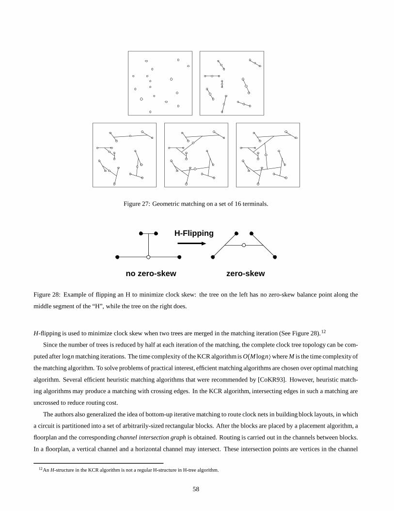
Figure 27: Geometric matching on a set of 16 terminals.
no zero-skew zero-skew
H-Flipping
Figure 28: Example of flipping an H to minimize clock skew: the tree on the left has no zero-skew balance point along the
middle segment of the “H”, while the tree on the right does.
H-flipping is used to minimize clock skew when two trees are merged in the matching iteration (See Figure 28).12
Since the number of trees is reduced by half at each iteration of the matching, the complete clock tree topology can be com-
puted after logn matching iterations. The time complexity of the KCR algorithm is O M logn where M is the time complexity of
the matching algorithm. To solve problems of practical interest, efficient matching algorithms are chosen over optimal matching
algorithm. Several efficient heuristic matching algorithms that were recommended by [CoKR93]. However, heuristic match-
ing algorithms may produce a matching with crossing edges. In the KCR algorithm, intersecting edges in such a matching are
uncrossed to reduce routing cost.
The authors also generalized the idea of bottom-up iterative matching to route clock nets in building block layouts, in which
a circuit is partitioned into a set of arbitrarily-sized rectangular blocks. After the blocks are placed by a placement algorithm, a
floorplan and the corresponding channel intersection graph is obtained. Routing is carried out in the channels between blocks.
In a floorplan, a vertical channel and a horizontal channel may intersect. These intersection points are vertices in the channel
12An H-structure in the KCR algorithm is not a regular H-structure in H-tree algorithm.
58
intersection graph. In the channel intersection graph, vertices u and v are connected by an edge if and only if there is a channel
from u to v not containing any other vertex. An augmented channel intersection graph (ACIG) is used to capture the location
of clock pins (or clock entry points) of functional elements. Each entry point is also a vertex in the ACIG. The entry point also
introduces an auxiliary vertex on the channel, and an edge is created between the block entry point and the auxiliary vertex in
order to complete the routing.
For the KCR algorithm to work in an ACIG, instead of using the geometric distance as the cost of the edge between two
subtrees, the shortest distance on the channel graph is used as the cost of the edge connecting two points. Therefore, an additional
component in the KCR algorithm for general cell design is the shortest path algorithm to compute the shortest paths between all
pairs of vertices in each iteration. For each pair of matched vertices, a balance point along the shortest path connecting the two
vertices is computed, and the balance point then serves as a vertex to be matched in the next iteration.
In general, the KCR algorithm performs better than the MMM algorithm, in terms of both routing cost and clock skew (under
the pathlengthdelay model). The algorithmswere evaluated using random point sets. Moreover, two MCNC benchmark circuits,
named Primary1 and Primary2, reported in [JaSK90] were also used in the experiment. No data for the BB method is available
since BB produces only an unembedded binary tree topology. Note that both the MMM and KCR algorithms cannot guarantee
zero-skew routing, although the routing solutions constructed by the KCR algorithm have skews very close to zero.
The two benchmark circuits Primary1 and Primary 2, together with the other five benchmark circuits r1 to r5 reported in
[Ts91], would later become the most commonly used benchmark circuits to evaluate the quality of routing solutions generated
by various clock routing algorithms. Otherwise specified, the experimental results reported by various papers will be presented
with respect to these benchmark circuits.
5.2 Embedding of Abstract Topology
Given a prescribed abstract topology, the Deferred-Merge Embedding (DME) algorithm, proposed independently by Edahiro
[Ed91], Chao, Hsu, and Ho [ChHH92a], and Boese and Kahng [BoKa92], achieves exact zero skew for both pathlength and
Elmore delay models. The enabling concept is that of a merging segment. The problem of bounded-skew embedding was
first addressed independently by Cong and Koh [CoKo95], and Huang, Kahng, and Tsao [HuKT95] under the pathlength delay
model. Cong et al. [CoKK95] later extended the works to handle bounded-skew embedding under the Elmore delay model. The
BST/DME algorithms proposed by [CoKo95, HuKT95, CoKK95] generalize the merging segment concept and introduce merg-
ing region for bounded-skew embedding. These embedding algorithms (both zero-skew and bounded-skew) can also be com-
bined with bottom-up topology generation to produce clock trees with less routing costs [Ed92, CoKo95, HuKT95, CoKK95].
5.2.1 Zero-Skew Embedding
The key idea of the DME algorithm is the delayed embedding of internal nodes of the abstract topology [Ed91, ChHH92a,
BoKa92]. In general, given two zero-skew trees, there can be a number of locations at which two zero-skew trees can be joined
with the minimum wirelength such that zero skew is achieved at the higher level. For example, in Figure 29(b), any point l x on the line segment ms x is equi-distant from sinks s1 and s2 , i.e., we obtain a zero-skew sub-tree rooted at l x with sinks s1
and s2 . This contrasts with the KCR algorithm where there is only a single balance point when two sub-trees are connected by
59
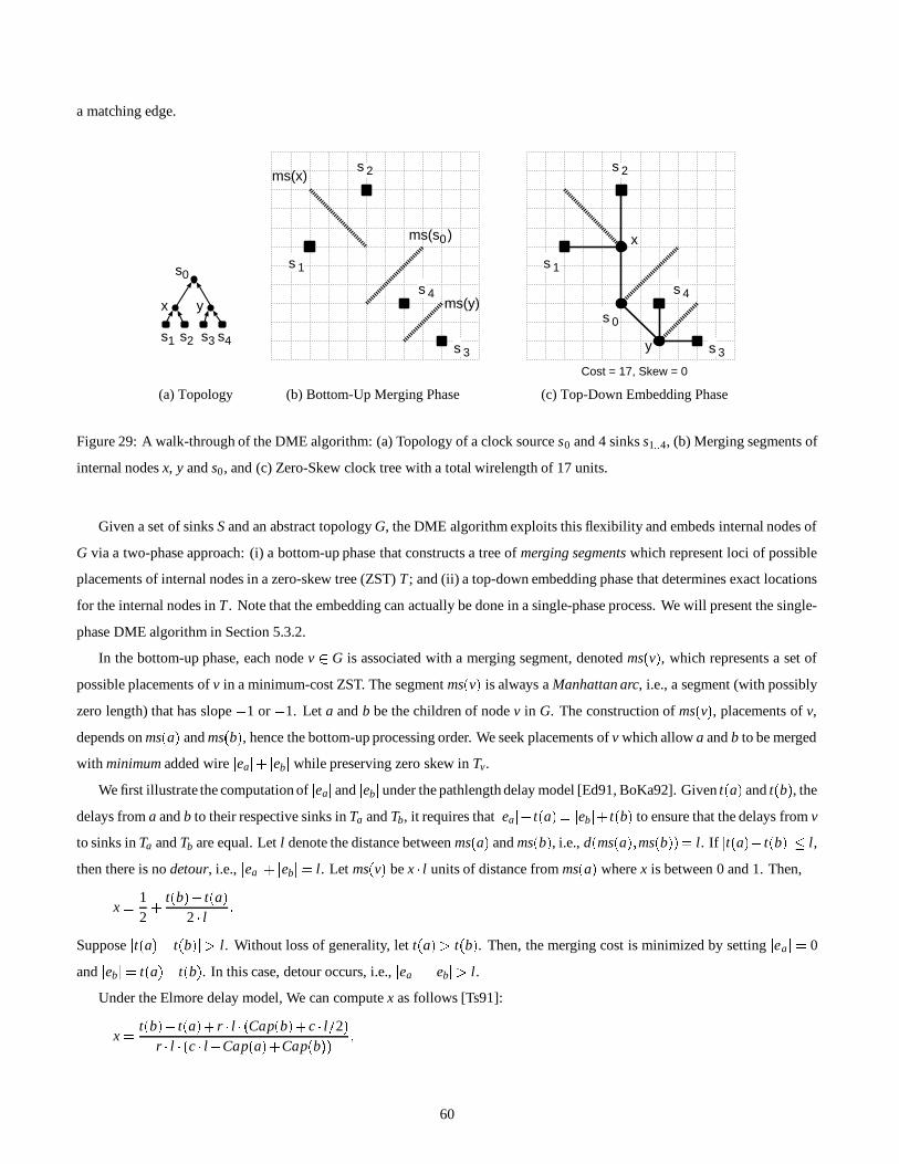
a matching edge.
x
ms(y)
ms(x)
ms(s )0
(b) Bottom-Up Merging Phase
s 1
s 2
s 3
s 4
s1 s2 s3 s4
x y
s0
(a) Topology (c) Top-Down Embedding Phase
Cost = 17, Skew = 0
s 0
s 1
s 2
s 3
s 4
y
Figure 29: A walk-through of the DME algorithm: (a) Topology of a clock source s0 and 4 sinks s1 4, (b) Merging segments of
internal nodes x, y and s0 , and (c) Zero-Skew clock tree with a total wirelength of 17 units.
Given a set of sinks S and an abstract topology G, the DME algorithm exploits this flexibility and embeds internal nodes of
G via a two-phase approach: (i) a bottom-up phase that constructs a tree of merging segments which represent loci of possible
placements of internal nodes in a zero-skew tree (ZST) T ; and (ii) a top-down embedding phase that determines exact locations
for the internal nodes in T . Note that the embedding can actually be done in a single-phase process. We will present the single-
phase DME algorithm in Section 5.3.2.
In the bottom-up phase, each node v G is associated with a merging segment, denoted ms v , which represents a set of
possible placements of v in a minimum-cost ZST. The segment ms v is always a Manhattan arc, i.e., a segment (with possibly
zero length) that has slope 1 or 1. Let a and b be the children of node v in G. The construction of ms v , placements of v,
depends on ms a and ms b , hence the bottom-up processing order. We seek placements of v which allow a and b to be merged
with minimum added wire ea eb while preserving zero skew in Tv.
We first illustrate the computation of ea and eb under the pathlength delay model [Ed91, BoKa92]. Given t a and t b , the
delays from a and b to their respective sinks in Ta and Tb, it requires that ea t a eb t b to ensure that the delays from v
to sinks in Ta and Tb are equal. Let l denote the distance between ms a and ms b , i.e., d ms a ms b l. If t a t b l,
then there is no detour, i.e., ea eb l. Let ms v be x l units of distance from ms a where x is between 0 and 1. Then,
x 12 t b t a
2 l
Suppose t a t b l. Without loss of generality, let t a t b . Then, the merging cost is minimized by setting ea 0
and eb t a t b . In this case, detour occurs, i.e., ea eb l.
Under the Elmore delay model, We can compute x as follows [Ts91]:
x t b t a r l Cap b c l 2 r l c l Cap a Cap b
60
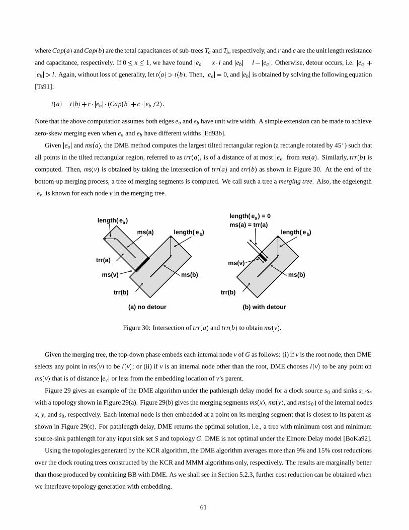
where Cap a and Cap b are the total capacitances of sub-trees Ta and Tb, respectively, and r and c are the unit length resistance
and capacitance, respectively. If 0 x 1, we have found ea x l and eb l ea . Otherwise, detour occurs, i.e. ea eb l. Again, without loss of generality, let t a t b . Then, ea 0, and eb is obtained by solving the following equation
[Ts91]:
t a t b r eb Cap b c eb 2
Note that the above computation assumes both edges ea and eb have unit wire width. A simple extension can be made to achieve
zero-skew merging even when ea and eb have different widths [Ed93b].
Given ea and ms a , the DME method computes the largest tilted rectangular region (a rectangle rotated by 45
) such that
all points in the tilted rectangular region, referred to as trr a , is of a distance of at most ea from ms a . Similarly, trr b is
computed. Then, ms v is obtained by taking the intersection of trr a and trr b as shown in Figure 30. At the end of the
bottom-up merging process, a tree of merging segments is computed. We call such a tree a merging tree. Also, the edgelength
ev is known for each node v in the merging tree.
length( ea)
length( eb)
ms(b)
ms(a)
trr(a)
trr(b)
(a) no detour (b) with detour
length( eb)
ms(b)
trr(b)
ms(a) = trr(a)length( ea) = 0
ms(v)
ms(v)
Figure 30: Intersection of trr a and trr b to obtain ms v .
Given the merging tree, the top-down phase embeds each internal node v of G as follows: (i) if v is the root node, then DME
selects any point in ms v to be l v ; or (ii) if v is an internal node other than the root, DME chooses l v to be any point on
ms v that is of distance ev or less from the embedding location of v’s parent.
Figure 29 gives an example of the DME algorithm under the pathlength delay model for a clock source s0 and sinks s1-s4
with a topology shown in Figure 29(a). Figure 29(b) gives the merging segments ms x , ms y , and ms s0 of the internal nodes
x, y, and s0, respectively. Each internal node is then embedded at a point on its merging segment that is closest to its parent as
shown in Figure 29(c). For pathlength delay, DME returns the optimal solution, i.e., a tree with minimum cost and minimum
source-sink pathlength for any input sink set S and topology G. DME is not optimal under the Elmore Delay model [BoKa92].
Using the topologies generated by the KCR algorithm, the DME algorithm averages more than 9% and 15% cost reductions
over the clock routing trees constructed by the KCR and MMM algorithms only, respectively. The results are marginally better
than those produced by combining BB with DME. As we shall see in Section 5.2.3, further cost reduction can be obtained when
we interleave topology generation with embedding.
61
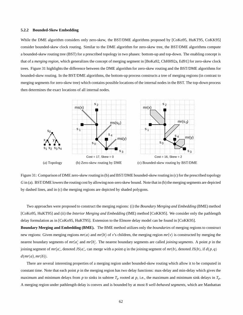
5.2.2 Bounded-Skew Embedding
While the DME algorithm considers only zero-skew, the BST/DME algorithms proposed by [CoKo95, HuKT95, CoKK95]
consider bounded-skew clock routing. Similar to the DME algorithm for zero-skew tree, the BST/DME algorithms compute
a bounded-skew routing tree (BST) for a prescribed topology in two phases: bottom-up and top-down. The enabling concept is
that of a merging region, which generalizes the concept of merging segment in [BoKa92, ChHH92a, Ed91] for zero-skew clock
trees. Figure 31 highlights the difference between the DME algorithm for zero-skew routing and the BST/DME algorithms for
bounded-skew routing. In the BST/DME algorithms, the bottom-up process constructs a tree of merging regions (in contrast to
merging segments for zero-skew tree) which contains possible locations of the internal nodes in the BST. The top-down process
then determines the exact locations of all internal nodes.
(b) Zero-skew routing by DME
Cost = 17, Skew = 0
s 0
s 1
s 2
s 3
s 0
s 1
s 2
s 3
(c) Bounded-skew routing by BST/DME
Cost = 16, Skew = 2
s1 s2 s3 s4
x y
s0
(a) Topology
ms(y)
ms(x)
ms(s )0
s 4 s 4
mr(x)
mr(y)
mr(s )0
Figure 31: Comparison of DME zero-skew routing in (b) and BST/DME bounded-skew routing in (c) for the prescribed topology
G in (a). BST/DME lowers the routingcost by allowing non-zero skew bound. Note that in (b) the merging segments are depicted
by dashed lines, and in (c) the merging regions are depicted by shaded polygons.
Two approaches were proposed to construct the merging regions: (i) the Boundary Merging and Embedding (BME) method
[CoKo95, HuKT95] and (ii) the Interior Merging and Embedding (IME) method [CoKK95]. We consider only the pathlength
delay formulation as in [CoKo95, HuKT95]. Extension to the Elmore delay model can be found in [CoKK95].
Boundary Merging and Embedding (BME). The BME method utilizes only the boundaries of merging regions to construct
new regions: Given merging regions mr a and mr b of v’s children, the merging region mr v is constructed by merging the
nearest boundary segments of mr a and mr b . The nearest boundary segments are called joining segments. A point p in the
joining segment of mr a , denoted JS a , can merge with a point q in the joining segment of mr b , denoted JS b , if d p q d mr a mr b .
There are several interesting properties of a merging region under bounded-skew routing which allow it to be computed in
constant time. Note that each point p in the merging region has two delay functions: max-delay and min-delay which gives the
maximum and minimum delays from p to sinks in subtree Tp rooted at p, i.e., the maximum and minimum sink delays in Tp .
A merging region under pathlength delay is convex and is bounded by at most 8 well-behaved segments, which are Manhattan
62
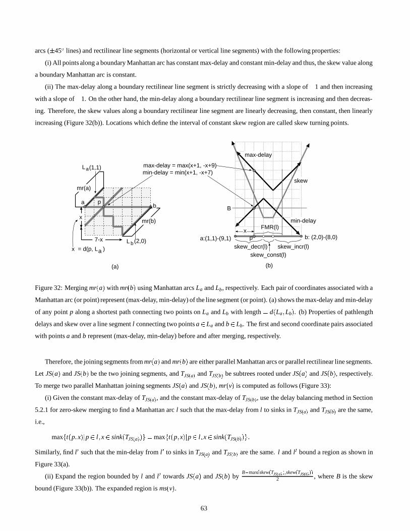
arcs (
45
lines) and rectilinear line segments (horizontal or vertical line segments) with the following properties:
(i) All points along a boundary Manhattan arc has constant max-delay and constant min-delay and thus, the skew value along
a boundary Manhattan arc is constant.
(ii) The max-delay along a boundary rectilinear line segment is strictly decreasing with a slope of 1 and then increasing
with a slope of 1. On the other hand, the min-delay along a boundary rectilinear line segment is increasing and then decreas-
ing. Therefore, the skew values along a boundary rectilinear line segment are linearly decreasing, then constant, then linearly
increasing (Figure 32(b)). Locations which define the interval of constant skew region are called skew turning points.
min-delay = min(x+1, -x+7)max-delay = max(x+1, -x+9)
skew_decr(l) skew_incr(l)a:(1,1)-(9,1) b: (2,0)-(8,0)
min-delay
skew
px
FMR(l)
B
(b)
skew_const(l)
max-delay
(a)
7-x
a
(1,1)La
(2,0)L b
b
mr(b)
mr(a)
x = d(p, L )a
x
p
Figure 32: Merging mr a with mr b using Manhattan arcs La and Lb , respectively. Each pair of coordinates associated with a
Manhattan arc (or point) represent (max-delay, min-delay) of the line segment (or point). (a) shows the max-delay and min-delay
of any point p along a shortest path connecting two points on La and Lb with length d La Lb . (b) Properties of pathlength
delays and skew over a line segment l connecting two points a La and b Lb. The first and second coordinate pairs associated
with points a and b represent (max-delay, min-delay) before and after merging, respectively.
Therefore, the joining segments from mr a and mr b are either parallel Manhattan arcs or parallel rectilinear line segments.
Let JS a and JS b be the two joining segments, and TJS a and TJS b be subtrees rooted under JS a and JS b , respectively.
To merge two parallel Manhattan joining segments JS a and JS b , mr v is computed as follows (Figure 33):
(i) Given the constant max-delay of TJS a , and the constant max-delay of TJS b , use the delay balancing method in Section
5.2.1 for zero-skew merging to find a Manhattan arc l such that the max-delay from l to sinks in TJS a and TJS b are the same,
i.e.,
maxt p x p l x sink TJS a max
t p x p l x sink TJS b
Similarly, find l such that the min-delay from l to sinks in TJS a and TJS b are the same. l and l bound a region as shown in
Figure 33(a).
(ii) Expand the region bounded by l and l towards JS a and JS b byB max skew TJS a skew TJS b
2 , where B is the skew
bound (Figure 33(b)). The expanded region is ms v .
63
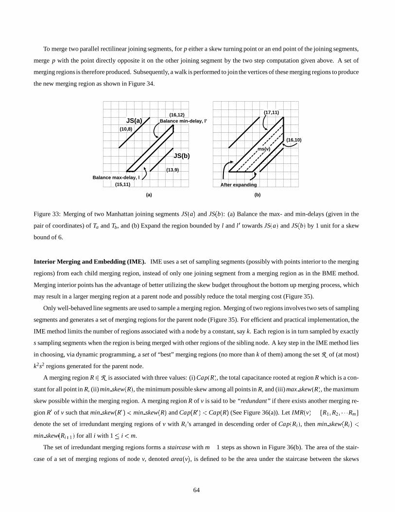
To merge two parallel rectilinear joining segments, for p either a skew turning point or an end point of the joining segments,
merge p with the point directly opposite it on the other joining segment by the two step computation given above. A set of
merging regions is therefore produced. Subsequently, a walk is performed to join the vertices of these merging regions to produce
the new merging region as shown in Figure 34.
(16,12)
(13,9)
(10,8)
Balance min-delay, l’
Balance max-delay, l
After expanding(15,11)
(17,11)
(16,10)
JS(a)
JS(b)
(a) (b)
ms(v)
Figure 33: Merging of two Manhattan joining segments JS a and JS b : (a) Balance the max- and min-delays (given in the
pair of coordinates) of Ta and Tb, and (b) Expand the region bounded by l and l towards JS a and JS b by 1 unit for a skew
bound of 6.
Interior Merging and Embedding (IME). IME uses a set of sampling segments (possibly with points interior to the merging
regions) from each child merging region, instead of only one joining segment from a merging region as in the BME method.
Merging interior points has the advantage of better utilizing the skew budget throughout the bottom up merging process, which
may result in a larger merging region at a parent node and possibly reduce the total merging cost (Figure 35).
Only well-behaved line segments are used to sample a merging region. Merging of two regions involves two sets of sampling
segments and generates a set of merging regions for the parent node (Figure 35). For efficient and practical implementation, the
IME method limits the number of regions associated with a node by a constant, say k. Each region is in turn sampled by exactly
s sampling segments when the region is being merged with other regions of the sibling node. A key step in the IME method lies
in choosing, via dynamic programming, a set of “best” merging regions (no more than k of them) among the set R of (at most)
k2s2 regions generated for the parent node.
A merging region R R is associated with three values: (i) Cap R , the total capacitance rooted at region R which is a con-
stant for all point in R, (ii) min skew R , the minimum possible skew among all points in R, and (iii) max skew R , the maximum
skew possible within the merging region. A merging region R of v is said to be “redundant” if there exists another merging re-
gion R of v such that min skew R min skew R and Cap R Cap R (See Figure 36(a)). Let IMR v R1 R2 Rm
denote the set of irredundant merging regions of v with Ri’s arranged in descending order of Cap Ri , then min skew Ri min skew Ri
1 for all i with 1 i m.
The set of irredundant merging regions forms a staircase with m 1 steps as shown in Figure 36(b). The area of the stair-
case of a set of merging regions of node v, denoted area v , is defined to be the area under the staircase between the skews
64
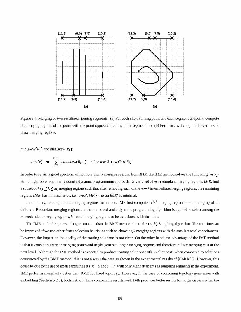
(11,3) (8,6) (7,5) (10,2)
(9,9)(11,7) (14,4)
(11,3) (8,6) (7,5) (10,2)
(9,9)(11,7) (14,4)
(a) (b)
Figure 34: Merging of two rectilinear joining segments: (a) For each skew turning point and each segment endpoint, compute
the merging regions of the point with the point opposite it on the other segment, and (b) Perform a walk to join the vertices of
these merging regions.
min skew R1 and min skew Rk :
area v m 1
∑i 1
min skew Ri
1 min skew Ri Cap Ri
In order to retain a good spectrum of no more than k merging regions from IMR, the IME method solves the following m k -Sampling problem optimally using a dynamic programming approach: Given a set of m irredundant merging regions, IMR, find
a subset of k (2 k m) merging regions such that after removing each of the m k intermediate merging regions, the remaining
regions IMR has minimal error, i.e., area IMR area IMR is minimal.
In summary, to compute the merging regions for a node, IME first computes k2s2 merging regions due to merging of its
children. Redundant merging regions are then removed and a dynamic programming algorithm is applied to select among the
m irredundant merging regions, k “best” merging regions to be associated with the node.
The IME method requires a longer run-time than the BME method due to the m k -Sampling algorithm. The run-time can
be improved if we use other faster selection heuristics such as choosing k merging regions with the smallest total capacitances.
However, the impact on the quality of the routing solutions is not clear. On the other hand, the advantage of the IME method
is that it considers interior merging points and might generate larger merging regions and therefore reduce merging cost at the
next level. Although the IME method is expected to produce routing solutions with smaller costs when compared to solutions
constructed by the BME method, this is not always the case as shown in the experimental results of [CoKK95]. However, this
could be due to the use of small sampling sets (k 5 and s 7) with only Manhattan arcs as sampling segments in the experiment.
IME performs marginally better than BME for fixed topology. However, in the case of combining topology generation with
embedding (Section 5.2.3), both methods have comparable results, with IME produces better results for larger circuits when the
65
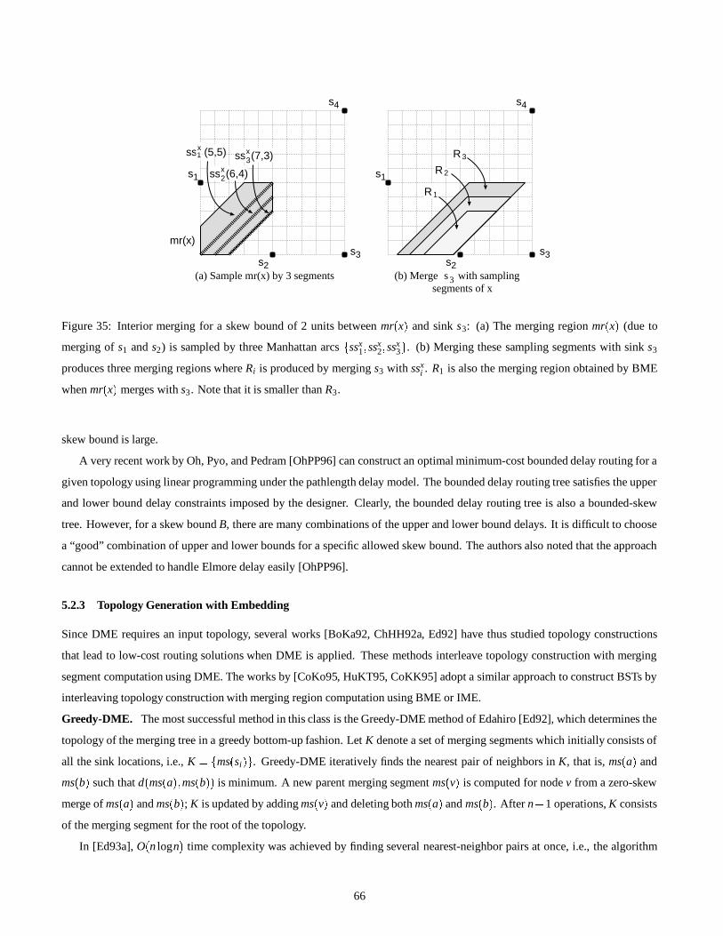
s1
s2
s4
(5,5)
s1
s2
s3
s4
mr(x)
(6,4)
(7,3)ss
ss
ss
R1
R2
R3
(a) Sample mr(x) by 3 segments (b) Merge s3 with samplingsegments of x
s3
x3
1x
x2
Figure 35: Interior merging for a skew bound of 2 units between mr x and sink s3: (a) The merging region mr x (due to
merging of s1 and s2) is sampled by three Manhattan arcsssx
1 ssx2 ssx
3 . (b) Merging these sampling segments with sink s3
produces three merging regions where Ri is produced by merging s3 with ssxi . R1 is also the merging region obtained by BME
when mr x merges with s3 . Note that it is smaller than R3 .
skew bound is large.
A very recent work by Oh, Pyo, and Pedram [OhPP96] can construct an optimal minimum-cost bounded delay routing for a
given topology using linear programming under the pathlength delay model. The bounded delay routing tree satisfies the upper
and lower bound delay constraints imposed by the designer. Clearly, the bounded delay routing tree is also a bounded-skew
tree. However, for a skew bound B, there are many combinations of the upper and lower bound delays. It is difficult to choose
a “good” combination of upper and lower bounds for a specific allowed skew bound. The authors also noted that the approach
cannot be extended to handle Elmore delay easily [OhPP96].
5.2.3 Topology Generation with Embedding
Since DME requires an input topology, several works [BoKa92, ChHH92a, Ed92] have thus studied topology constructions
that lead to low-cost routing solutions when DME is applied. These methods interleave topology construction with merging
segment computation using DME. The works by [CoKo95, HuKT95, CoKK95] adopt a similar approach to construct BSTs by
interleaving topology construction with merging region computation using BME or IME.
Greedy-DME. The most successful method in this class is the Greedy-DME method of Edahiro [Ed92], which determines the
topology of the merging tree in a greedy bottom-up fashion. Let K denote a set of merging segments which initially consists of
all the sink locations, i.e., K ms si . Greedy-DME iteratively finds the nearest pair of neighbors in K, that is, ms a and
ms b such that d ms a ms b is minimum. A new parent merging segment ms v is computed for node v from a zero-skew
merge of ms a and ms b ; K is updated by adding ms v and deleting both ms a and ms b . After n 1 operations, K consists
of the merging segment for the root of the topology.
In [Ed93a], O n logn time complexity was achieved by finding several nearest-neighbor pairs at once, i.e., the algorithm
66
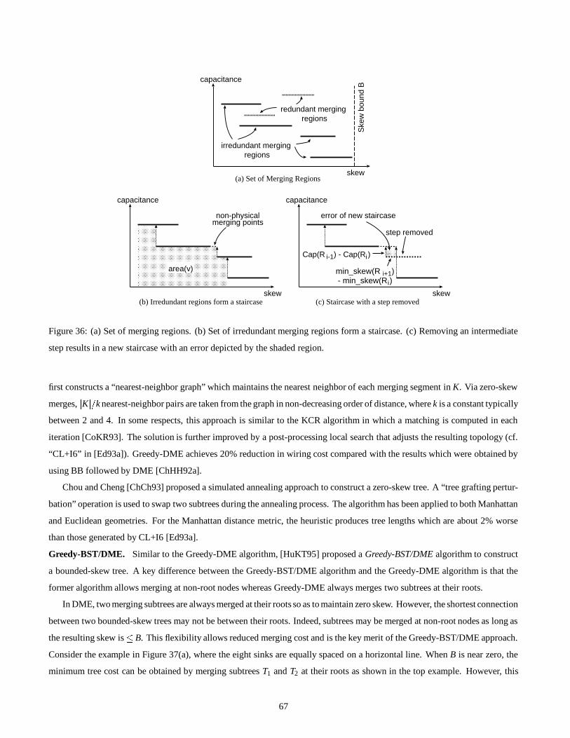
redundant merging regions
Ske
w b
ound
B
skew
capacitance
(a) Set of Merging Regions
skew
capacitance
(b) Irredundant regions form a staircaseskew
capacitance
(c) Staircase with a step removed
step removed
error of new staircase
irredundant merging regions
area(v) min_skew(R )- min_skew(R )
i+1i
Cap(R ) - Cap(R )i-1 i
non-physicalmerging points
Figure 36: (a) Set of merging regions. (b) Set of irredundant merging regions form a staircase. (c) Removing an intermediate
step results in a new staircase with an error depicted by the shaded region.
first constructs a “nearest-neighbor graph” which maintains the nearest neighbor of each merging segment in K. Via zero-skew
merges, K k nearest-neighbor pairs are taken from the graph in non-decreasing order of distance, where k is a constant typically
between 2 and 4. In some respects, this approach is similar to the KCR algorithm in which a matching is computed in each
iteration [CoKR93]. The solution is further improved by a post-processing local search that adjusts the resulting topology (cf.
“CL+I6” in [Ed93a]). Greedy-DME achieves 20% reduction in wiring cost compared with the results which were obtained by
using BB followed by DME [ChHH92a].
Chou and Cheng [ChCh93] proposed a simulated annealing approach to construct a zero-skew tree. A “tree grafting pertur-
bation” operation is used to swap two subtrees during the annealing process. The algorithm has been applied to both Manhattan
and Euclidean geometries. For the Manhattan distance metric, the heuristic produces tree lengths which are about 2% worse
than those generated by CL+I6 [Ed93a].
Greedy-BST/DME. Similar to the Greedy-DME algorithm, [HuKT95] proposed a Greedy-BST/DME algorithm to construct
a bounded-skew tree. A key difference between the Greedy-BST/DME algorithm and the Greedy-DME algorithm is that the
former algorithm allows merging at non-root nodes whereas Greedy-DME always merges two subtrees at their roots.
In DME, two merging subtrees are always merged at their roots so as to maintain zero skew. However, the shortest connection
between two bounded-skew trees may not be between their roots. Indeed, subtrees may be merged at non-root nodes as long as
the resulting skew is B. This flexibility allows reduced merging cost and is the key merit of the Greedy-BST/DME approach.
Consider the example in Figure 37(a), where the eight sinks are equally spaced on a horizontal line. When B is near zero, the
minimum tree cost can be obtained by merging subtrees T1 and T2 at their roots as shown in the top example. However, this
67

(a)
5 6 7 81 2 3 4
rT1 T2
rT’1 T’2
r
1 2
3
4u
v
1 2
3
4r’
u
v
(b)
Figure 37: (a) An example showing that given skew bound B
0, changing the subtree topology before merging will reduce
the merging cost. (b) Repositioning the root in changing the topology.
topology is bad when B is large, even if the costs of the two subtrees can be minimum. When the skew bound is large, ideally
one should adjust the subtree topology so that the roots of subtrees become closer while the subtree costs remain the same or
increase slightly. This is shown in the bottom example in Figure 37(a). Effectively, T1 and T2 are merged at non-root nodes.
Figure 37(b) illustrates in more details how the tree topology is adjusted. First, the root is moved down to some tree edge,
say eu uv, so that the root becomes the parent of nodes u and v. Then the tree topology is adjusted accordingly by adding,
deleting, and redirecting some edges. The costs of the two subtrees may increase but the overall cost of the tree after merging
may be better.
Merging with non-root nodes is a powerful topology generation method. The work by [CoKo95] is a simple extension of
Greedy-DME, i.e., it considers merging of root nodes only. The wirelength reduction averages 19% when the allowed skew
increases from 0 to ∞. The Greedy-BST/DME algorithm by [HuKT95] can achieve an average of 42% wirelength reduction
when varying the skew bound from 0 to ∞. In fact, it very closely matches the performance of the best-known heuristics for
both the zero-skew [Ed93a, Ed94] and infinite-skew limiting cases, i.e. Steiner routing (Section 3.1.2).
For realistic skew bounds in the range of 0ps to 150ps, the Greedy-BST/DME algorithms in [CoKK95] averages 26.6%
wirelength reduction when compared to the best reported zero-skew solutions by the CL+I6 algorithm in [Ed93a].
5.3 Planar Clock Routing
It is preferable to route clock nets on the metal layer with the smallest RC delay since this avoids the use of vias in the clock
net and makes the layout more tolerant of process-variations. This motivates the following papers on planar clock routing. In
these papers, they assumes Euclidean planarity, i.e. all edges in the tree do not cross when an edge is represented by a straight
line segment (instead of rectilinear line segments for the Manhattan geometry) on a Euclidean plane. Nevertheless, the cost of
an edge is still in the Manhattan distance metric. It is not difficult to see that given a routing solution with Euclidean planarity,
we can always embed a straight Euclidean segment by a rectilinear staircase to get a planar rectilinear routing solution.
68
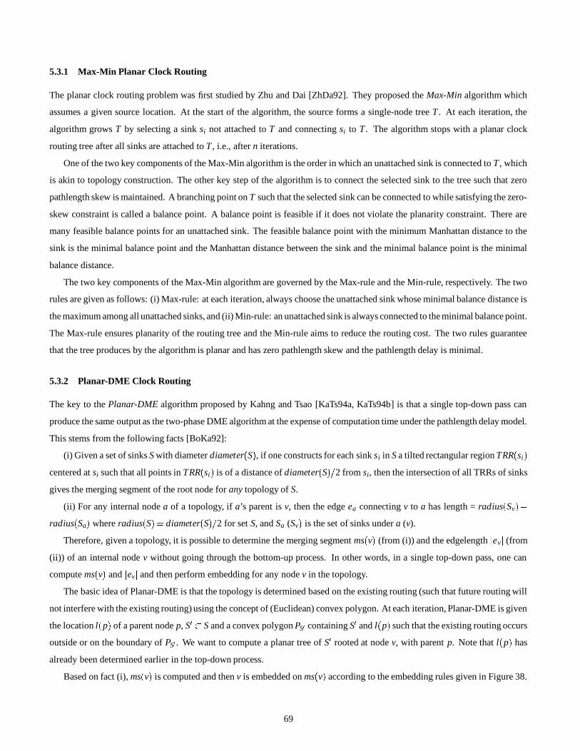
5.3.1 Max-Min Planar Clock Routing
The planar clock routing problem was first studied by Zhu and Dai [ZhDa92]. They proposed the Max-Min algorithm which
assumes a given source location. At the start of the algorithm, the source forms a single-node tree T . At each iteration, the
algorithm grows T by selecting a sink si not attached to T and connecting si to T . The algorithm stops with a planar clock
routing tree after all sinks are attached to T , i.e., after n iterations.
One of the two key components of the Max-Min algorithm is the order in which an unattached sink is connected to T , which
is akin to topology construction. The other key step of the algorithm is to connect the selected sink to the tree such that zero
pathlength skew is maintained. A branching point on T such that the selected sink can be connected to while satisfying the zero-
skew constraint is called a balance point. A balance point is feasible if it does not violate the planarity constraint. There are
many feasible balance points for an unattached sink. The feasible balance point with the minimum Manhattan distance to the
sink is the minimal balance point and the Manhattan distance between the sink and the minimal balance point is the minimal
balance distance.
The two key components of the Max-Min algorithm are governed by the Max-rule and the Min-rule, respectively. The two
rules are given as follows: (i) Max-rule: at each iteration, always choose the unattached sink whose minimal balance distance is
the maximum among all unattached sinks, and (ii) Min-rule: an unattached sink is always connected to the minimal balance point.
The Max-rule ensures planarity of the routing tree and the Min-rule aims to reduce the routing cost. The two rules guarantee
that the tree produces by the algorithm is planar and has zero pathlength skew and the pathlength delay is minimal.
5.3.2 Planar-DME Clock Routing
The key to the Planar-DME algorithm proposed by Kahng and Tsao [KaTs94a, KaTs94b] is that a single top-down pass can
produce the same output as the two-phase DME algorithm at the expense of computation time under the pathlength delay model.
This stems from the following facts [BoKa92]:
(i) Given a set of sinks S with diameter diameter S , if one constructs for each sink si in S a tilted rectangular region TRR si centered at si such that all points in TRR si is of a distance of diameter S 2 from si, then the intersection of all TRRs of sinks
gives the merging segment of the root node for any topology of S.
(ii) For any internal node a of a topology, if a’s parent is v, then the edge ea connecting v to a has length = radius Sv
radius Sa where radius S diameter S 2 for set S, and Sa (Sv is the set of sinks under a (v).
Therefore, given a topology, it is possible to determine the merging segment ms v (from (i)) and the edgelength ev (from
(ii)) of an internal node v without going through the bottom-up process. In other words, in a single top-down pass, one can
compute ms v and ev and then perform embedding for any node v in the topology.
The basic idea of Planar-DME is that the topology is determined based on the existing routing (such that future routing will
not interfere with the existing routing) using the concept of (Euclidean) convex polygon. At each iteration, Planar-DME is given
the location l p of a parent node p, S S and a convex polygon PS containing S and l p such that the existing routing occurs
outside or on the boundary of PS . We want to compute a planar tree of S rooted at node v, with parent p. Note that l p has
already been determined earlier in the top-down process.
Based on fact (i), ms v is computed and then v is embedded on ms v according to the embedding rules given in Figure 38.
69
The embedding rules ensure that v is embedded within PS and so the routing from p to v is within PS and does not interfere
with the existing routing. Based on the relative locations of p and v, a splitting line is then defined according to the partitioning
rules given in Figure 38. The splitting line divides PS into two convex polygons PS 1and PS 2
and therefore, partitions S into two
non-empty subsets S 1 and S 2. Note that the splitting allows the routing from p to v to be on the boundary between PS 1and PS 2
and therefore, all existing routing is outside PS 1and PS 2
. The algorithm then recursively operates on S 1 and S 2 .
IV.2
IV.1
IV.3
II.2II.3
II.1
I
III
c(ms(v)) = mid-point of ms(v)
p
p
1
2
The Embedding Rules
Location of p Embedding point of v
Region I or III c(ms(v))
Region II.1 or IV.1 intersection of p1 p2 with horizon-
tal line through l p Region II.3 or IV.3 intersection of p1 p2 with vertical
line through l p Region II.2 (IV.2) p2 (p1)
The Partitioning Rules
Location of p, v Splitting line
l p l v Line through l p l v l p l v c ms v Line through p1 p2
l p l v c ms v Vertical line through l p Figure 38: Rules to choose the embedding point of v on ms v p1 p2 and the splitting line to partition a sink set.
Kahng and Tsao [KaTs94b] later extended the Planar-DME algorithm from the pathlength delay model in [KaTs94a] to the
Elmore delay model. The Elmore-Planar-DME algorithm uses the topology generated by the Planar-DME algorithm under the
pathlength delay model, and then reconstructs the ZST in a bottom-upfashion: Planar embedding is applied to all planar subtrees
at the same level in the topology; given a pair of sibling planar subtrees, their parent node is embedded to ensure planarity by
(i) finding the shortest planar path between its two children and (ii) embedding the parent node at some point along the planar
path. The DME algorithm for Elmore delay model is then applied to ancestors of the parent nodes. In other words, a tree of
merging segments is re-constructed to embed the ancestors of the parent nodes. Another iteration of planar embedding followed
by DME is then applied at the next higher level. This continues until the entire ZST is planar. For a topology of height h, the
Elmore-Planar-DME algorithm uses h iterations of planar embedding followed by DME.
The Max-Min and Planar-DME algorithms achieve planarity through higher routing costs. It is interesting to note that the
Max-Min algorithm produces X-tree-like solutions, whereas the Planar-DME algorithms produce H-tree-like structures. As
mentioned, X-trees tend to be more costly than H-trees. The Planar-DME algorithms incur only an average penalty of 9 9%
additional routing cost to achieve planarity while the planar clock trees generated by the Max-Min algorithm have an average
of 35% higher routing cost when compared to the best (non-planar) zero-skew solutions in [Ed93a].
5.4 Buffer and Wire Sizing for Clock Nets
In this section, we deal with buffer and wire sizing, which consider sizing of wires, and insertion and sizing of buffers in clock
routing to minimize clock skew, clock delay, and the sensitivity of the clock tree to process variations, which may cause the
70
width of a wire/transistor on a chip to differ from the specified width and/or device parameters such as carrier mobilities and
threshold voltages to vary from die to die. Process variations introduce process skew since resistances and capacitances of wires
and active devices are changed.
Consider a RC tree. From Section 2.1, the Elmore delay from the clock driver at the source s0 to sink si is ti Rd Cap s0 ∑ev
Path s0 si ev r wev
ev
wev ca2 Cap v . For simplicity, we ignore the fringing effect but it can be added easily into our
formulation. Taking the partial differential ∂ti∂wev
for any edge ev along the s0–si path,
∂ti∂wev
Rd ca ev
ev r Cap v w2
ev
∑eu
Ans ev
eu r ca ev weu
(32)
If ev is not along Path s0 si ,∂ti
∂wev
Rd ca ev ∑eu
Ans ev Path s0 si
eu r ca ev weu
(33)
The partial differential captures the delay sensitivity with respect to a wire. A positive value of sensitivity indicates a case
where widening the wire increases the delay while a negative value of sensitivity indicates that the delay decreases. If we com-
pute the optimal wire width to minimize sink delay (for example, by setting ∂ti∂wev
0 for Eqn. (32)), we see that wires closer to
the root should have wider wire width, since they drive larger capacitance (Cap v ). Note that the term Rd ca ev in the equa-
tion prevents the wire ev from getting too wide. In practice, we can always impose an upper bound constraint on the maximum
wire width.
Also observe that the larger the downstream capacitance (Cap v ), the larger the delay sensitivity (Eqn. (32)). Buffer inser-
tion can de-sensitize the clock nets by reducing downstream capacitance of wires closer to the root. In other words, sink delay
can be minimized by appropriate wiresizing and buffer insertion. Similarly, we can also define the delay sensitivity due to buffer
by writing the sink delay in terms of the buffer sizes and taking the partial differential of the delay with respect to the buffer sizes.
It is obvious that appropriate buffer/driver sizing can also reduce delay sensitivity.
We are also interested in skew sensitivity, which measures how a change in wire/transistor width can affect the clock skew.
In particular, skew sensitivity due to process variations can be used to measure how reliable a clock tree is. However, due to the
definition of clock skew as maxi j ti t j , it is very difficult and costly to compute skew sensitivity exactly; the exact approach
would have to compute the worst case clock skew due to process variations. The following approach may be used to estimate
skew sensitivity [XiDa95]. To compute the estimated worst case clock skew, the algorithm computes for each sink s i, the best
possible and worst possible delay due to process variations. For simplicity, the algorithm computes the worst (best) delay for
sink si by decreasing (increasing) the wire widths for edges on Path s0 si by ∆wmax and increasing (decreasing) the wire widths
of all edges off the path by ∆wmax, where ∆wmax is the maximum width variations. The worst case skew under process variations
is obtained by taking the difference between the worst case delay of one sink and the best case delay of another sink. The dif-
ference between the skew of the clock tree (without process variations) and the worst case skew under process variations gives
a reasonable estimate of the skew sensitivity. Note that we can use a similar approach to estimate the skew sensitivity due to
deviations of transistor widths and device parameters caused by process variations.
In this section, we discuss various wire sizing, buffer insertion and buffer sizing techniques which make use of delay sensi-
tivity and skew sensitivity to guide the optimization. These methods not only reduce the delay and skew sensitivities, but also
have significant effect on reductions of wirelength, rise/fall times, and power dissipation.
71

5.4.1 Wiresizing in Clock Routing
In the following, we discuss three results on wiresizing. The first algorithm achieves minimal skew by making slower paths faster
by wiresizing [ZhDX93] (instead of making the faster paths slower by snaking in the DME approach). The second approach
considers wiresizing to minimize clock delay and uses the DME approach to ensure zero skew [Ed93b]. The third heuristic
considers not only the nominal skew due to sink delays but also the process skew. At the same time, it tries to meet a specified
target delay [PuMP93].
Both [ZhDX93, PuMP93] assume discrete wire sizes, whereas [Ed93b] assumes continuous wire width although it can also
be modified to consider discrete wire widths. Since it is not possible to achieve arbitrary precision during fabrication, it is better to
have a layout with discrete wire widths and transistor sizes in order to eliminate skew due to mapping of continuous widths/sizes
to discrete widths/sizes. [ZhDX93] can handle constraint on the maximum wire width whereas [Ed93b, PuMP93] can be ex-
tended easily to consider maximum wire width constraint. Note that the constraint on the maximum wire width is imposed by
the available routing resource. On the other hand, the constraint on the minimum wire width is due to the fabrication technology.
Moreover, the maximum allowable current density through the wire also provides a lower bound for the wire width, so that the
wire can withstand the wear-out phenomenon called electromigration. Note that different segments of wires may have different
upper and lower bounds.
The Optimal Sizing Method (OSM) proposed by Zhu, Dai, and Xi [ZhDX93] considers distributedRC and lossy transmission
line models using a generalized delay macromodel which is based on scattering-parameters of interconnect [LiDW93]. Also, it
can handle general clock network which may includes loops. The skew minimization problem is formulated as a least-squares
estimation problem: the error of a sink si is defined to be gi ti t f where t f is the least delay among all source-to-sink delays.
The least-squares estimation problem aims to assign widths to the m wires in the general network such that the sum of squares
of error φ w1 w2 wm ∑ni 1 g2
i is minimized.
The OSM uses the Gauss-Marquardt’s method [Ma63] to solve the optimization problem. The Gauss-Marquardt’s method
takes an initial wire width assignment, Wi and compute a new wire width assignment Wi
1 based on a n m delay sensitivity
matrix for a clock tree/mesh of n sinks and m edges. The i j -th entry of the sensitivity matrix measures the delay sensitivity of
sink si with respect to edge e j , i.e., ∂ti∂we j
. In the next iteration, Wi
1 is used to update the error φ and delay sensitivity matrix for
the computation of Wi
2. The procedure continues until the skew is reduced to a required value. The key to fast convergence
is a good starting point W0. The following rules are applied to guide the initial wire width assignment: (i) the edges in the tree
are sized in the breadth first search order, (ii) at each level, the ancestor edges of the slowest terminal is sized first, and (iii) each
edge is assigned with the feasible width that results in the smallest skew. The three rules can be generalized to handle buffered
clock tree.
A clock mesh and two clock trees were used to evaluate the OSM algorithm under both RC model and lossy transmission
line model. [ZhDX93] reported smaller skews for optimized circuits when compared to the original circuits. The authors noted
that the skew reduction should be more significant for clock trees than for clock meshes since stronger interaction among clock
sinks in clock meshes results in less skew sensitivity with respect to wire widths. The skew reduction is achieved at the expense
of an average of 200% additional wiring area. The clock delay may get worse in some cases.
Edahiro [Ed93b] proposed a wiresizing algorithm which performs wiresizing based on delay sensitivity due to wire to min-
imize clock delay. The algorithm constructs a clock tree in two phases. In the first phase, the algorithm applies Greedy-DME
72
[Ed92] to construct a pathlength balanced clock topology with edgelength information. Using the topology computed in the first
phase, the second phase of the algorithm applies a modified version of DME under Elmore delay to construct a wiresized clock
routing tree.
The modified DME algorithmworks as follows. Consider merging of two zero-skew subtrees Ta and Tb. The optimal widthof
the two edges ea and eb merging Ta and Tb is first computed using an approach similar to setting Eqn. (32) to zero and then solving
it. Note that the optimal width assignment should actually depend on both upstream resistance and downstream capacitance as
in Eqn. (32). Since the wire widths at the upstream are unknowns in the bottom process, they are approximated. For example,
nominal wire widths may be used for the upstream edges. Then, with consideration of wea and web , the minimum merging cost
ea eb is computed using a similar approach by [Ts91] (see Section 5.2.1). At the end of the bottom-upmerging, the top-down
embedding of the original DME approach is applied to obtain a wiresized clock tree.
The wiresized clock trees constructed by [Ed93b] satisfy the zero skew constraint while achieving 10%-50% shorter total
delay time than the un-sized clock trees in [Ed93a]. However, no result on the increase in wiring area is reported. Although
the algorithm does not place a upper-bound constraint on the wire width, the computed wire widths are not expected to get too
large since the algorithm consider the clock driver strength. Since the computed edgelengths differ from the original pathlength
balanced tree and the wire widths may be far from optimal due to the approximation, it is recommended that the second phase
(i.e., the modified DME algorithm) be repeated for a few iterations. However, it is not clear if the process will converge (i.e.,
edgelengths and wire widths do not change in two successive applications of the modified DME algorithm). Note that since wire
widths are selected based on delay sensitivity, delay sensitivityof the clock tree due to process variations is minimized indirectly.
In [PuMP93], Pullela, Menezes, and Pillage optimized the wire widths in three steps to achieve a reliable non-zero skew
clock tree under the Elmore delay model:
(i) The first step selects the suitable wires to widen in order to bring the average delay of the tree to a specified target delay,
denoted ttgt . Each edge ev is assigned a cost Dv ∑ni 1
∂ti∂wev
ti ttgt . Note that if ti ttgt and ∂ti∂wev
0, Dv decreases. At
each iteration, the wire with the least cost is widened by a constant amount ∆w, which is the minimum grid size based on the
fabrication technology. The process continues until the target delay ttgt is achieved.
(ii) The second step tries to minimize the process skew by de-sensitizing all sink delays. The algorithm uses a single-defect
model where the width of a single wire ev changes due to a single process variation. If ∆wmax is the maximum change in width
due to process variations, the maximum change in delay is ∆wmax ∂ti∂wev
. To ensure the change in skew is within the maximum
allowable change in skew ∆B, the width wev is widened such that ∆wmax ∂ti∂wev
∆B l where l is the depth of the tree. Therefore,
if all edges along a source-to-sink path change their widths, the total change in delay is still less than ∆B.
(iii) The final step aims to reduce the nominal skew, or simply, the skew. Let ∆tiv denote the change in the delay of sink si
when the width of wire wev is changed by ∆w. ∆tiv is estimated by ∆w ∂ti∂wev
. Zero skew is achieved when ∆tiv tave ti for all
sinks si in the tree, where tave is the average delay. Each edge wev is assigned a cost Dv ∑ni 1 ti ∆tiv tave . If there is a
wire with zero cost, zero skew is achieved. Otherwise, a wire with the least cost is chosen to be widened by ∆w since the goal
is to find a wire with zero cost quickly.
However, step i may undo what step i 1 has accomplished. To prevent step (iii) from undoing the de-sensitization process
in step (ii), [PuMP93] suggested tracing back from the widened edge in step (iii) to the root, and widening wires on the way up
to ensure ∆wmax ∂ti∂wev
∆B l holds. However, it is not clear how we can prevent steps (ii) and (iii) from messing up the work
73
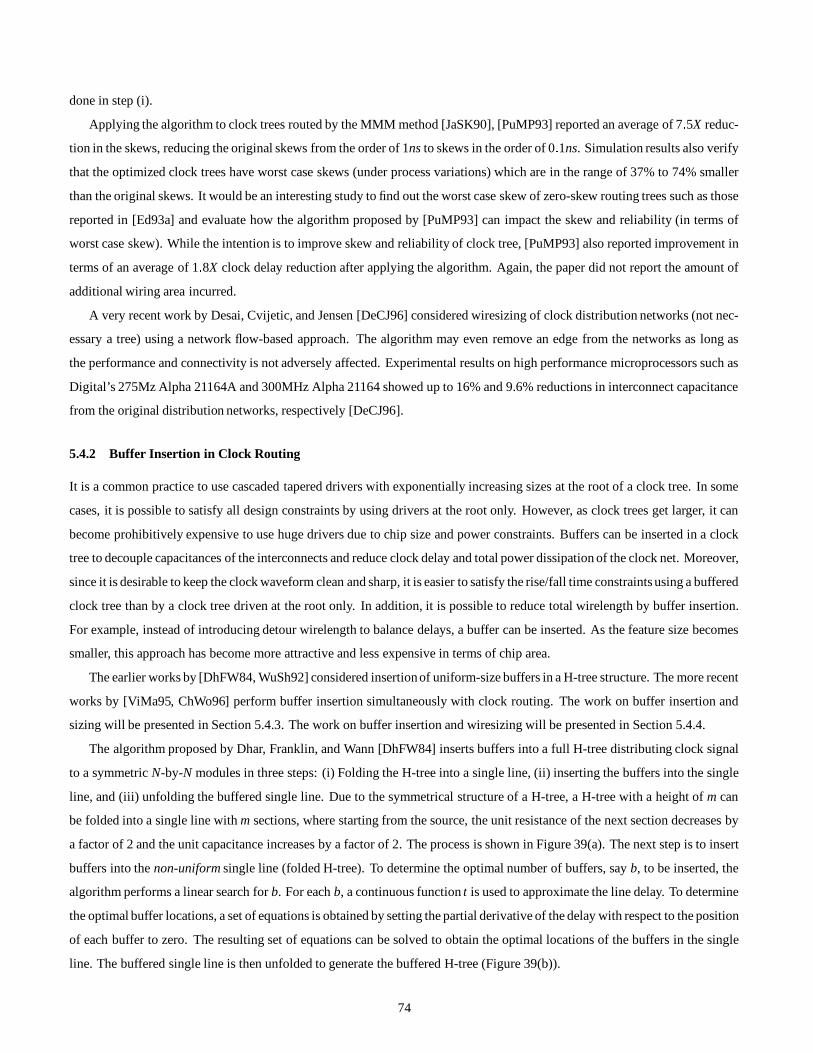
done in step (i).
Applying the algorithm to clock trees routed by the MMM method [JaSK90], [PuMP93] reported an average of 7 5X reduc-
tion in the skews, reducing the original skews from the order of 1ns to skews in the order of 0 1ns. Simulation results also verify
that the optimized clock trees have worst case skews (under process variations) which are in the range of 37% to 74% smaller
than the original skews. It would be an interesting study to find out the worst case skew of zero-skew routing trees such as those
reported in [Ed93a] and evaluate how the algorithm proposed by [PuMP93] can impact the skew and reliability (in terms of
worst case skew). While the intention is to improve skew and reliability of clock tree, [PuMP93] also reported improvement in
terms of an average of 1 8X clock delay reduction after applying the algorithm. Again, the paper did not report the amount of
additional wiring area incurred.
A very recent work by Desai, Cvijetic, and Jensen [DeCJ96] considered wiresizing of clock distribution networks (not nec-
essary a tree) using a network flow-based approach. The algorithm may even remove an edge from the networks as long as
the performance and connectivity is not adversely affected. Experimental results on high performance microprocessors such as
Digital’s 275Mz Alpha 21164A and 300MHz Alpha 21164 showed up to 16% and 9.6% reductions in interconnect capacitance
from the original distribution networks, respectively [DeCJ96].
5.4.2 Buffer Insertion in Clock Routing
It is a common practice to use cascaded tapered drivers with exponentially increasing sizes at the root of a clock tree. In some
cases, it is possible to satisfy all design constraints by using drivers at the root only. However, as clock trees get larger, it can
become prohibitively expensive to use huge drivers due to chip size and power constraints. Buffers can be inserted in a clock
tree to decouple capacitances of the interconnects and reduce clock delay and total power dissipation of the clock net. Moreover,
since it is desirable to keep the clock waveform clean and sharp, it is easier to satisfy the rise/fall time constraints using a buffered
clock tree than by a clock tree driven at the root only. In addition, it is possible to reduce total wirelength by buffer insertion.
For example, instead of introducing detour wirelength to balance delays, a buffer can be inserted. As the feature size becomes
smaller, this approach has become more attractive and less expensive in terms of chip area.
The earlier works by [DhFW84, WuSh92] considered insertionof uniform-size buffers in a H-tree structure. The more recent
works by [ViMa95, ChWo96] perform buffer insertion simultaneously with clock routing. The work on buffer insertion and
sizing will be presented in Section 5.4.3. The work on buffer insertion and wiresizing will be presented in Section 5.4.4.
The algorithm proposed by Dhar, Franklin, and Wann [DhFW84] inserts buffers into a full H-tree distributing clock signal
to a symmetric N-by-N modules in three steps: (i) Folding the H-tree into a single line, (ii) inserting the buffers into the single
line, and (iii) unfolding the buffered single line. Due to the symmetrical structure of a H-tree, a H-tree with a height of m can
be folded into a single line with m sections, where starting from the source, the unit resistance of the next section decreases by
a factor of 2 and the unit capacitance increases by a factor of 2. The process is shown in Figure 39(a). The next step is to insert
buffers into the non-uniform single line (folded H-tree). To determine the optimal number of buffers, say b, to be inserted, the
algorithm performs a linear search for b. For each b, a continuous function t is used to approximate the line delay. To determine
the optimal buffer locations, a set of equations is obtained by setting the partial derivative of the delay with respect to the position
of each buffer to zero. The resulting set of equations can be solved to obtain the optimal locations of the buffers in the single
line. The buffered single line is then unfolded to generate the buffered H-tree (Figure 39(b)).
74
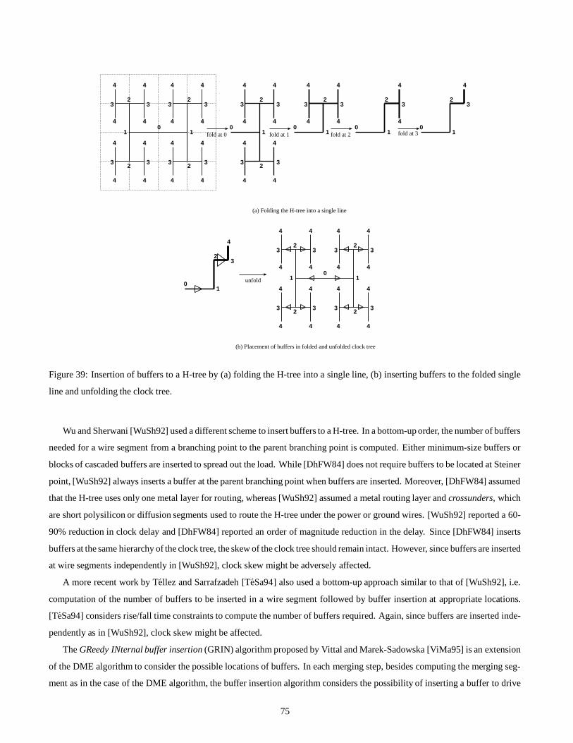
01 1
2
2 2
2
3333
4444
4444
4444
4444
3333
01
2
2
33
44
44
44
44
33
01
2
44
44
33
01
2
4
4
3
01
2
4
3
fold at 0 fold at 1 fold at 2 fold at 3
(a) Folding the H-tree into a single line
(b) Placement of buffers in folded and unfolded clock tree
01 1
2
2 2
2
3333
4444
4444
4444
4444
3333
01
2
4
3
unfold
Figure 39: Insertion of buffers to a H-tree by (a) folding the H-tree into a single line, (b) inserting buffers to the folded single
line and unfolding the clock tree.
Wu and Sherwani [WuSh92] used a different scheme to insert buffers to a H-tree. In a bottom-up order, the number of buffers
needed for a wire segment from a branching point to the parent branching point is computed. Either minimum-size buffers or
blocks of cascaded buffers are inserted to spread out the load. While [DhFW84] does not require buffers to be located at Steiner
point, [WuSh92] always inserts a buffer at the parent branching point when buffers are inserted. Moreover, [DhFW84] assumed
that the H-tree uses only one metal layer for routing, whereas [WuSh92] assumed a metal routing layer and crossunders, which
are short polysilicon or diffusion segments used to route the H-tree under the power or ground wires. [WuSh92] reported a 60-
90% reduction in clock delay and [DhFW84] reported an order of magnitude reduction in the delay. Since [DhFW84] inserts
buffers at the same hierarchy of the clock tree, the skew of the clock tree should remain intact. However, since buffers are inserted
at wire segments independently in [WuSh92], clock skew might be adversely affected.
A more recent work by Tellez and Sarrafzadeh [TeSa94] also used a bottom-up approach similar to that of [WuSh92], i.e.
computation of the number of buffers to be inserted in a wire segment followed by buffer insertion at appropriate locations.
[TeSa94] considers rise/fall time constraints to compute the number of buffers required. Again, since buffers are inserted inde-
pendently as in [WuSh92], clock skew might be affected.
The GReedy INternal buffer insertion (GRIN) algorithm proposed by Vittal and Marek-Sadowska [ViMa95] is an extension
of the DME algorithm to consider the possible locations of buffers. In each merging step, besides computing the merging seg-
ment as in the case of the DME algorithm, the buffer insertion algorithm considers the possibility of inserting a buffer to drive
75
one of the child subtrees. For example, consider two subtrees Ta and Tb rooted at a and b, respectively. Let v be the parent of a
and b. Then, ms v shown in Figure 40(c) can be computed as in the DME algorithm and it corresponds to the feasible locations
of v when no buffer is inserted.
A buffer to drive Ta alone may be inserted at the start of the edge from v to a as shown in Figure 40(a). The Manhattan arc Va
corresponds to the feasible locations of v for such a configuration. Note that Va is nearer to ms a than ms v since the delay to
sinks under a is now longer. Alternatively, the buffer may be inserted at ms a as shown in Figure 40(b) and the Manhattan arc V acorresponds to the feasible locations of v for this alternative arrangement. Clearly, Va and V a captures the two extreme possible
locations of the buffer. The shaded region bounded by Va and V a corresponds to other possible locations of the buffer (between
the start of edge ea and end of edge ea) with the minimum merging cost. Note that Va may be farther from ms a depending on
the total capacitance rooted at a and the buffer parasitics (resistance and input capacitance). Similarly, a buffer may be inserted
to drive Tb alone. The shaded region between ms b and ms v shows the feasible locations of v when a buffer is inserted to
drive Tb.
b
a
a b a b
vv
ms(v)V
V’
a
a
(a) (b)
(c)
Figure 40: Insertion of a buffer at different locations along the edge ea to drive Ta alone.
The GRIN algorithm follows the flow of the Greedy-DME algorithm of [Ed93a] with the following modifications. Instead
of using just wirelength to define merging cost, the cost of merging is defined to reflect both total wirelength and total buffer
size. Also, instead of storing only a merging segment in the DME approach, a merging segment and two polygons are stored
to reflect the possibilities of buffer insertion. At the next level of merging, the merging segment or polygon that yields locally
minimum zero skew merging cost will be used for merging with that of sibling node. On top of considering buffer insertion
during merging, buffer maybe inserted to drive the merged subtree if the rise/fall time constraint is very stringent.
Compared to clock trees driven by cascaded drivers at the root only, the buffered clock trees constructed by the GRIN algo-
rithm have significantly better rise/fall times. The buffer/driver area required by the GRIN algorithm is more than 6X smaller
and the algorithm averages 2X reduction in power dissipation. Compared to the zero-skew solutions reported in [Ed93a], the
clock delay reduction is also very significant. The results also showed shorter clock delays when compared to the wiresized
76

zero-skew solutions in [Ed93b].
A shortcoming of inserting buffers to balance clock signal delay is that buffers, being active devices, potentially heighten
the sensitivity of signal delay (and hence skew) to process variations. In most works on buffered clock tree, (for example, those
to be discussed below), buffers are inserted at the same levels of the clock tree. Therefore, all source-to-sink paths have equal
number of buffers inserted along the path. Moreover, buffers at the same level have the same size. These restrictions may affect
the optimality in terms of signal delay and total wirelength. However, they help to reduce skew sensitivity to process variations.
Chen and Wong [ChWo96] also considered buffer insertion and topology generation simultaneously. Instead of considering
buffer insertion at each merging step as in the GRIN algorithm, [ChWo96] considers inserting buffers at the roots of all subtrees.
Starting with a set S of subtrees, the algorithm performs several iterations of DME-based zero-skew merging [Ed91, ChHH92a,
BoKa92] until the size of S is reduced by 2k for some k (which is dependent on the strength of buffer). Note that this is akin
to clustering of nodes, followed by buffer insertion to drive each cluster. An inserted buffer may not be connected to the root
directly. Instead, a wire may be used to connect from the buffer output to the root of the subtree such that all subtrees in S
have equal sink delay. Note that this approach is less sensitive to process variations since all source-to-sink paths have the same
number of buffers. Experimental results also showed that both signal delay and total wirelengthare reduced when buffer insertion
is considered [ChWo96].
Related works in the area of buffered clock tree synthesis also include [ChSa93, RaSh89]. Assuming that all internal nodes
of a clock routing tree will be inserted with buffers, Cho and Sarrafzadeh [ChSa93] considered distributing the buffers over the
routing plane at the expense of minimum increase in routing cost to reduce local buffer congestion. The chip is first decomposed
into several square subregions, say r of them. Subregion Ri is represented by the center of mass Si of the sink set Pi in Ri. A
cluster spanning graph (CSG) is constructed such that the nodes in the CSG are sinks s1 n and centers S1 r. Unless they are
sinks, two nodes u, v are connected if d u v is within a user-specified vicinity parameter.
The authors want to construct a degree-distributed spanning tree (DDST) such that: (i) Each sink is connected to a unique
center. Let the degree of a center be the number of sinks connected to it. Then, (ii) the DDST should have the smallest standard
deviation in terms of the degrees of centers. Moreover, they want a minimum-length DDST, i.e., a DDST whose tree length is
the smallest among all DDST of CSG. An approximation algorithm is used to solve this NP-complete problem. Note that the
minimum-length DDST partitions the sinks into clusters, with each cluster of sinks rooted by a center. Finally, the KCR algo-
rithms is applied to generate the buffered clock tree, with the consideration that sinks in the same cluster are matched. [ChSa93]
reported that buffer congestion is reduced by 20% at the cost of 10% increase in wirelength. However, with a buffer inserted at
every internal node of the clock tree, this is a very expensive (in terms of power and delay) buffer distribution scheme.
Ramanathan and Shin [RaSh89] considered clock routing in an augmented channel intersection graph (ACIG). Given an
abstract (buffered) topology, the algorithm first finds the best location along the peripheral of the ACIG for the clock source in
order to minimize the clock delay. Next, with consideration of pathlength delay balancing, optimal routing at each level of the
buffered tree is carried out using a branch-and-bound approach. Note that this approach is only applicable to small problem
instances since it is computationally very expensive.
77
5.4.3 Buffer Insertion and Sizing in Clock Routing
While GRIN [ViMa95] considers construction of clock topology with buffer insertion, the balanced Buffer Insertion and Sizing
(BIS) algorithm proposed by Xi and Dai [XiDa95] assumes a given unbuffered clock tree and insert buffers of multiple sizes
to meet wire skew constraint due to asymmetric loads and wire width variations. Since the inserted buffers may have delay
variations due to variations of process parameters such as carrier mobilities and threshold voltages which may vary in a wide
range from die to die due to difference in process conditions, the second step of the BIS algorithm is to size the PMOS and
NMOS devices in the buffers separately to minimize power dissipation subject to tolerable skew constraint due to buffers. Note
that the BIS algorithm uses minimum width wire throughout the entire design in order to minimize wire capacitance and power
dissipation.
The BIS algorithm takes as input a pathlength balanced clock tree (possibly obtained by DME algorithm under pathlength
formulation) and partitions the clock tree into subtrees such that every subtree is a pathlength balanced subtree and all source to
sink paths go through equal number of levels of buffers. If L is the pathlength of the original clock tree and there are b number
of buffer levels, then the pathlength between the pathlength between two adjacent levels of buffers is L b 1 . To determine
the optimal b, the BIS algorithm considers minimization of the worst case skew due to process variations in wire widths. The
algorithm performs a linear search for b
from 1 2 until the worst case skew is less than a user-specified skew bound.
In the buffer sizing step, BIS considers CMOS inverters, each implemented by a PMOS and an NMOS device with size d pi
and dni , respectively. A PMOS device may have a nominal rise time tr, a fast rise time t f
r tr fp , or a slow rise time tsr tr fp ,
with fp 1. Similarly, we can define the nominal, fast and slow fall times of a NMOS device. Considering the pull-up devices
and pull-down devices along a path separately, let t pi (tn
i ) denote the total pull-up (pull-down) path delay due to PMOS (NMOS)
devices of even (odd) inverters along the s0–si path, then the delay to sink si due to buffers is ti tpi tn
i . Both power dissipation
(see [WeEs93]) and phase delay (under a model similar to the simple switch-level RC model) due to buffers are convex functions
of dpi and dn
i .
The key to the BIS algorithm is to transform the skew constraint to a convex function as follows: If the devices are sized
such that
tki tk
j εk Bb
2 fk (34)
for any two sinks si and s j, and k P N, then the skew constraint Bb for buffers can always be satisfied. The skew constraint
can be rewritten as a convex function as max tki εk tk
min where tkmin is the smallest pull-up path or pull-down path delays for
k P N among all source-to-sink paths. Given a device sizing solution, one can identify the fastest pull-up and pull-down path
and calculate tpmin and tn
min easily. BIS then uses t pmin and tn
min in Eqn. (36) of the following posynomial program and applies the
posynomial programming technique to solve the problem:
Minimize: Total Power Dissipation
subject to: max ti ttgt (35)
max tki εk tk
min for k P N (36)
If the computed device sizing solution satisfies the target delay ttgt constraint Eqn. (35) and the skew constraints Eqn. (36), then
78
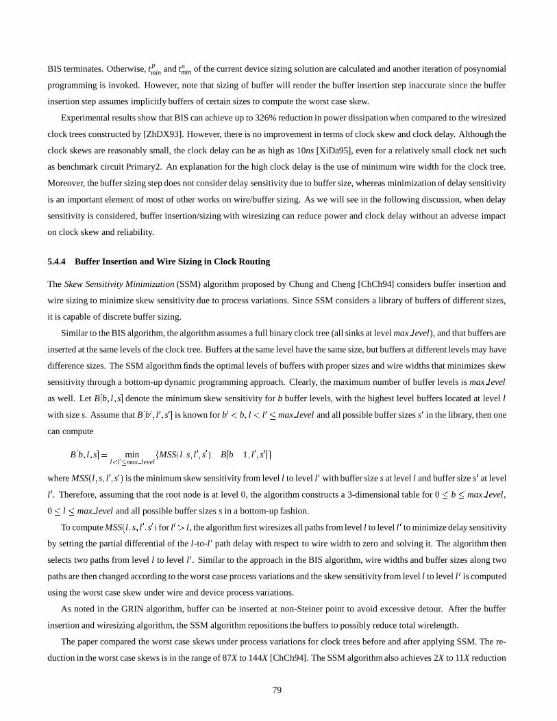
BIS terminates. Otherwise, t pmin and tn
min of the current device sizing solution are calculated and another iteration of posynomial
programming is invoked. However, note that sizing of buffer will render the buffer insertion step inaccurate since the buffer
insertion step assumes implicitly buffers of certain sizes to compute the worst case skew.
Experimental results show that BIS can achieve up to 326% reduction in power dissipation when compared to the wiresized
clock trees constructed by [ZhDX93]. However, there is no improvement in terms of clock skew and clock delay. Although the
clock skews are reasonably small, the clock delay can be as high as 10ns [XiDa95], even for a relatively small clock net such
as benchmark circuit Primary2. An explanation for the high clock delay is the use of minimum wire width for the clock tree.
Moreover, the buffer sizing step does not consider delay sensitivity due to buffer size, whereas minimization of delay sensitivity
is an important element of most of other works on wire/buffer sizing. As we will see in the following discussion, when delay
sensitivity is considered, buffer insertion/sizing with wiresizing can reduce power and clock delay without an adverse impact
on clock skew and reliability.
5.4.4 Buffer Insertion and Wire Sizing in Clock Routing
The Skew Sensitivity Minimization (SSM) algorithm proposed by Chung and Cheng [ChCh94] considers buffer insertion and
wire sizing to minimize skew sensitivity due to process variations. Since SSM considers a library of buffers of different sizes,
it is capable of discrete buffer sizing.
Similar to the BIS algorithm, the algorithm assumes a full binary clock tree (all sinks at level max level), and that buffers are
inserted at the same levels of the clock tree. Buffers at the same level have the same size, but buffers at different levels may have
difference sizes. The SSM algorithm finds the optimal levels of buffers with proper sizes and wire widths that minimizes skew
sensitivity through a bottom-up dynamic programming approach. Clearly, the maximum number of buffer levels is max level
as well. Let Bb l s denote the minimum skew sensitivity for b buffer levels, with the highest level buffers located at level l
with size s. Assume that Bb l s is known for b b, l l max level and all possible buffer sizes s in the library, then one
can compute
Bb l s min
l l max level
MSS l s l s B
b 1 l s
where MSS l s l s is the minimum skew sensitivity from level l to level l with buffer size s at level l and buffer size s at level
l . Therefore, assuming that the root node is at level 0, the algorithm constructs a 3-dimensional table for 0 b max level,
0 l max level and all possible buffer sizes s in a bottom-up fashion.
To compute MSS l s l s for l l, the algorithm first wiresizes all paths from level l to level l to minimize delay sensitivity
by setting the partial differential of the l-to-l path delay with respect to wire width to zero and solving it. The algorithm then
selects two paths from level l to level l . Similar to the approach in the BIS algorithm, wire widths and buffer sizes along two
paths are then changed according to the worst case process variations and the skew sensitivity from level l to level l is computed
using the worst case skew under wire and device process variations.
As noted in the GRIN algorithm, buffer can be inserted at non-Steiner point to avoid excessive detour. After the buffer
insertion and wiresizing algorithm, the SSM algorithm repositions the buffers to possibly reduce total wirelength.
The paper compared the worst case skews under process variations for clock trees before and after applying SSM. The re-
duction in the worst case skews is in the range of 87X to 144X [ChCh94]. The SSM algorithm also achieves 2X to 11X reduction
79

in clock delay.
Pullela et al. [PuMO93] also proposed a buffer insertion/sizing and wire sizing algorithm for a tree of l levels. Based on
the most critical resources to be optimized, the algorithm first estimate the number of buffer levels, denoted b. For b stages of
buffer, the algorithm try all possible level combinations to find the optimal levels in which buffers should be inserted. The skew
resource B is equally distributed among the clock tree such that the tolerable skew constraint of buffer, denoted Bb , and tolerable
skew constraint for interconnect, denoted Bw due to process variations are Bb Bw B l b for each subtree. As in the SSM
algorithm, subtrees at the same level are driven by buffers of the same size. The algorithm aims to achieve the followings: (i)
each subtree is nominally zero-skew by wiresizing and possibly introducing detour wire, (ii) each subtree have equal delay and
equal effective capacitance by assigning appropriate size and length to the stub of interconnect connecting a buffer to the root
of the subtree, and (iii) each subtree is driven by the smallest buffer that achieve the required skew constraints.
To achieve (i), the algorithm computes in a bottom-up fashion, the wire and length of each edge in the subtree such that
zero skew is achieved. Based on the wire skew constraint Bw and computing the maximum change in delay ∆tw induced by a
change in the width of an edge due to process variations, the minimum width of the edge required such that ∆tw Bw 2 can be
estimated.13 By applying an approach similar to [Ts91] with the lengths and widths as variables, the widths and lengths of the
two edges are computed to satisfy the estimated minimum width constraints and some prespecified maximum width constraint.
Detour is avoided when absolutely possible.
In (ii), by introducing a stub of interconnect from the buffer to the root of the subtree, it is always possible to achieve equal
interconnect delay for all subtrees at the same level. To match the effective capacitance (so that each subtree can be driven by
buffers of the same size), the length and width of the stub is chosen such that the ratio of the first two moments given in the π-
model are matched. To achieve objective (iii), we note that given a buffer size, the worst case skew ∆skewb induced by changes
in buffer sizes due to process variations can be computed easily (since all buffers at the same level have equal size and they drive
equal load). The smallest buffer size that satisfies the constraint ∆skewb Bb is chosen.
Simulation results show that delay reduction is achieved, with up to 25X reduction for large circuits when compared to the
wiresized clock trees constructed in [PuMP93]. By buffer insertion, [PuMO93] also reduces the maximum wire width required
for reliability (compared to [PuMP93]). This translates to reduction in total wiring area and therefore power dissipation. It was
observed that for delay (and power-delay product) minimization, the optimal number of buffer levels is close to half the number
of levels in the tree [PuMO93].
We note that buffer insertion algorithms such as those in [DhFW84, WuSh92, TeSa94, ViMa95, ChWo96, XiDa95] do not
restrict buffers to be located at branching points only, whereas the algorithms by [ChCh94, PuMO93] consider buffer insertion
at branching points only.
Chen, Chang, and Wong [ChCW96a] very recently proposed a simultaneous buffer and wire sizing algorithm based on La-
grangian relaxation. The algorithm minimizes clock skew by iteratively assigning appropriate weights (or Lagrangian multipli-
ers) to sinks and performing device and wire sizing based on a weighted-sum formulation similar to those in [CoLe95, CoKo94,
BoKR93]. Please refer to Section 4.2.2 for more details.
13The actual value cannot be computed since the upstream resistance is not known a priori and the length of the edge is only an estimate.
80
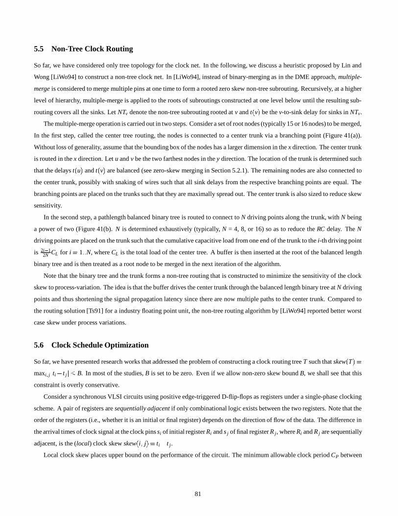
5.5 Non-Tree Clock Routing
So far, we have considered only tree topology for the clock net. In the following, we discuss a heuristic proposed by Lin and
Wong [LiWo94] to construct a non-tree clock net. In [LiWo94], instead of binary-merging as in the DME approach, multiple-
merge is considered to merge multiple pins at one time to form a rooted zero skew non-tree subrouting. Recursively, at a higher
level of hierarchy, multiple-merge is applied to the roots of subroutings constructed at one level below until the resulting sub-
routing covers all the sinks. Let NTv denote the non-tree subrouting rooted at v and t v be the v-to-sink delay for sinks in NTv.
The multiple-merge operation is carried out in two steps. Consider a set of root nodes (typically 15 or 16 nodes) to be merged,
In the first step, called the center tree routing, the nodes is connected to a center trunk via a branching point (Figure 41(a)).
Without loss of generality, assume that the bounding box of the nodes has a larger dimension in the x direction. The center trunk
is routed in the x direction. Let u and v be the two farthest nodes in the y direction. The location of the trunk is determined such
that the delays t u and t v are balanced (see zero-skew merging in Section 5.2.1). The remaining nodes are also connected to
the center trunk, possibly with snaking of wires such that all sink delays from the respective branching points are equal. The
branching points are placed on the trunks such that they are maximally spread out. The center trunk is also sized to reduce skew
sensitivity.
In the second step, a pathlength balanced binary tree is routed to connect to N driving points along the trunk, with N being
a power of two (Figure 41(b). N is determined exhaustively (typically, N = 4, 8, or 16) so as to reduce the RC delay. The N
driving points are placed on the trunk such that the cumulative capacitive load from one end of the trunk to the i-th driving point
is 2i 12N CL for i 1 N, where CL is the total load of the center tree. A buffer is then inserted at the root of the balanced length
binary tree and is then treated as a root node to be merged in the next iteration of the algorithm.
Note that the binary tree and the trunk forms a non-tree routing that is constructed to minimize the sensitivity of the clock
skew to process-variation. The idea is that the buffer drives the center trunk through the balanced length binary tree at N driving
points and thus shortening the signal propagation latency since there are now multiple paths to the center trunk. Compared to
the routing solution [Ts91] for a industry floating point unit, the non-tree routing algorithm by [LiWo94] reported better worst
case skew under process variations.
5.6 Clock Schedule Optimization
So far, we have presented research works that addressed the problem of constructing a clock routing tree T such that skew T maxi j ti t j B. In most of the studies, B is set to be zero. Even if we allow non-zero skew bound B, we shall see that this
constraint is overly conservative.
Consider a synchronous VLSI circuits using positive edge-triggered D-flip-flops as registers under a single-phase clocking
scheme. A pair of registers are sequentially adjacent if only combinational logic exists between the two registers. Note that the
order of the registers (i.e., whether it is an initial or final register) depends on the direction of flow of the data. The difference in
the arrival times of clock signal at the clock pins si of initial register Ri and s j of final register R j, where Ri and R j are sequentially
adjacent, is the (local) clock skew skew i j ti t j.
Local clock skew places upper bound on the performance of the circuit. The minimum allowable clock period CP between
81
L
AB
C
D
E
AB
C
D
E
(a) center chunk (b) balanced length binary tree
branchingpoint driving
point
F G H I
J K
Figure 41: (a) A center trunk connecting 5 sinks (b) A rooted balanced length binary tree at L driving the center trunk at 4
positions.
two sequentially adjacent registers Ri and R j satisfies the following inequality [WeEs93]:
CP t Li j skew i j tsu tds (37)
where t Li j is the delay for the data to travel through combinational logic Li j from Ri to R j , tsu is the setup time of the registers,
and tds is the propagation delay within the register. Note that for the data to be latched into the final register correctly, it must be
ready tsu units of time before the triggering clock edge. Also note that the term t Li j can be further decomposed into t Li j tinterconnect Li j tgate Li j , where tinterconnect Li j is the interconnect delay and tgate Li j is the gate delay. We use tmax Li j to
denote the longest path delay through Li j and tmin Li j to denote the shortest path delay through Li j.
If clock signal is not properly scheduled, clock hazards may occur. For example, data may reach the final register at too late a
time, or the data may race through the fast path and destroy the correct data at the final register before the correct data is latched.
To eliminate clock hazards, we impose the following constraints [Fr95]:
skew i j CP tsu tds tmax Li j skew i j tmin Li j tds thold (38)
where thold is the amount of time the input data signal must remain stable once the clock signal changes state. Therefore, if
skew i j is positive, it always decreases the maximum attainable clock frequency. However, if we examine the inequality re-
garding clock period in Eqn. (37), negative clock skew, i.e., skew i j 0, actually increases the effective clock period. In other
words, we can actually improve the performance of the system by introducing negative clock skew as long as Eqn. (38) is not
violated.
We can conclude that the clock skew is only relevant for sequentially adjacent registers and the clock skew between registers
on different data paths does not affect the performance and reliability of the synchronous system. Therefore, it is not necessary
to construct a zero-skew routing tree. In fact, it may be desirable to have (negative) clock skew. Moreover, different pairs of
sequentially adjacent registers may have different skew constraints (since the delays due to different combinational logic blocks
82
are likely to be different).
There are several works on clock schedule optimization. However, these works did not consider clock routing. For example,
Fishburn [Fi90] used linear programming to compute the optimal clock arrival times at the sinks such that either the clock period
CP is minimized or the safety margin for clock error given a prescribed clock period is maximized while constraints similar to
those in Eqn. (38) are satisfied. While the gate sizes in the logic block remain unchanged throughout the optimization process
in [Fi90], [ChSH93a, SaSF95] removed this restriction and considered gate sizing in the clock schedule optimization process
in order to achieve faster clock rate. While [Fi90, ChSH93a, SaSF95] assumed a fixed network of registers, in [Fr92b, SoFr94,
SoFM95], the authors considered retiming using skew information to optimize the circuit. Registers may be removed or inserted
as long the circuit still operates correctly.
A related problem on clock schedule optimization is to construct a clock tree that satisfies the clock schedule. Given a clock
schedule, Neves and Friedman [NeFr93, NeFr94, NeFr95] construct an (abstract) topology of the clock distributionnetwork and
determine the delay values at each branch of the clock network. Their works are mainly targeted for hierarchical data path design
[NeFr93, NeFr94, NeFr95]. However, they did not give a specific routing algorithm to embed the abstract topology. Seki et al.
[SeIK94] proposed a clock router that can accomplish specified delay using multiple routing layers. Very similar to the center
tree routing step in the non-tree clock routing algorithm proposed by [LiWo94], it uses a center trunk and routes from branching
point on the trunk to sinks with snaking where necessary.
A more recent work by Xi and Dai [XiDa96] considers clock schedule optimization with clock tree construction and gate
sizing. The proposed useful skew tree (UST) algorithm first generates an abstract topology using a top-down bipartitioning ap-
proach. The bipartitioning process is guided by the objective of producing useful negative skew. Sinks should be partitioned
into groups that have loose skew constraints. Sequentially adjacent registers across two groups should have the same logic path
direction. A useful skew tree (UST) is then constructed using bottom-up merging and top-down embedding from the abstract
topology. Since it is a non-zero skew merging, bottom-up merging produces merging regions. Similar to IME, it uses a set of
merging segments to sample a merging region. However, it uses only a merging segment from the set to generate the merg-
ing region of the parent. After the initial UST is constructed, the UST algorithm uses a simulated annealing process to explore
the solution space. A merging segment perturbation operation is used to select a different merging segment for the merging
operation. Note that this changes the clock routing tree configuration, and therefore, the clock schedule and skews. After each
merging segment perturbation operation, the UST algorithm performs gate sizing of combinational logic blocks to reduce power
dissipation.
The UST heuristic has been evaluated using three ISCAS89 benchmark circuits [BrBK89] and two industry circuits. In all but
one case, the UST algorithm uses less wirelength when compared to the Greedy-BST/DME [CoKo95, HuKT95] and BB+DME
algorithms [ChHH92b]. For each circuit, the skew bound for BST construction [CoKo95, HuKT95] is set to be the smallest
skew bound of all sink pairs. To compare the impact of a UST on power dissipation, [XiDa96] also performed gate sizing with
bounded (zero) skew after a BST (ZST) was constructed. The power reductions achieved by the UST approach vary from 11%
to 22% over the BST and ZST approaches.
83
6 Conclusion and Future Work
In this paper, we presented an up-to-date survey of the design and optimization techniques for VLSI interconnect layout. These
results show convincingly that interconnect optimization has a significant impact on circuit performance in deep submicron
VLSI design. In this section, we would like to offer a brief summary with our assessment of various interconnect optimization
techniques presented in this paper, and suggest directions for future research.
1. Interconnect topology optimization: We feel that geometric based Steiner tree algorithms such as the A-tree [CoLZ93],
Alphabetic Tree [ViMa94], P-Tree [LiCL96b] algorithms usually provide a good initial routing topology. These algorithms use
the right level of abstraction and can be incorporated in a global router efficiently. Further delay reduction can be achieved
by refining the initial topology, for example, using the techniques presented in [BoOI94, BoKR93, ViMa94, XuKu95b]. Most
effective topology optimization for delay reduction is achieved by considering routing tree construction with buffer insertion
as discussed in [OkCo96a, OkCo96b, LiCL96a]. However, more studies need to be done on how to extend various routing
tree construction algorithms to take into consideration of multiple-layer routing with different RC characteristics in each layer,
presence of routing obstacles, and routability optimization.
2. Device and interconnect sizing: The optimization problems in this area usually have well defined mathematical program-
ming formulations. We feel that the sensitivity based heuristics, such as those used in [FiDu85, Sa94], and the local refine-
ment technique based on the dominance property (and the bundled refinement property) used in [CoLe95, CoKo94, CoHe95,
CoHe96c] are most efficient, produce good quality solutions, and scale up well with the rapid increasing of design complex-
ity. The initial device and interconnect sizing solutions can be computed using a simple switch-level driver model and Elmore
delay model as in [FiDu85, CoLe95, CoKo94] and then more accurate driver and interconnect models, such as those used in
[MePP95, MeBP95] can be applied to further refine the solution for performance and area optimization.
3. Clock routing: Various interconnect optimization techniques presented in this paper have most significant impact on clock
routing due to the extremely large size of clock nets. Extensive studies of the clock routing problem in the past few years have
made much advance on automating high-performance clock net synthesis. The bottom-up construction methods using the DME
technique (e.g., [Ed91, ChHH92a, BoKa92, CoKK95, ViMa95]) are most promising in terms of efficiency, flexibility, and the
solution quality. Most existing approaches first produce a balanced routing topology and then perform buffer insertion, buffer
and wire sizing. More studies need to be done on how to generate a clock tree topology together with buffer insertion, buffer
sizing, and wire sizing to meet the skew, delay, power dissipation, and other constraints.
In addition to the interconnect optimization techniques in the areas presented in this paper, we think that the following topics
are also very important to the development of next generation interconnect-driven layout systems, but have not received full
attention from the VLSI CAD research community. We would like to suggest them as future research directions.
1. More accurate and efficient delay models for interconnect optimization: Most of existing works on interconnect optimiza-
tion are based on the Elmore delay model due to its simplicity, explicit representation of signal delay in terms of interconnect
design parameters, and fairly high fidelity under the current fabrication technology [BoKM93, CoHe96a, CoKK95]. However,
limitations of the Elmore delay model are well recognized as it cannot be used to characterize the signal waveform, handle in-
terconnect inductance, and model frequency-dependent effects. Although more accurate delay models are available, they were
mainly developed for circuit simulation and do not provide an explicit causal relationship between signal responses and design
84
parameters for optimization. Therefore, there is a strong need to bridge the gap between the timing models used for circuit
simulation and circuit and interconnect optimization. The recent work on efficient moment computation [YuKu95a], low-order
moment matching [Ho84, ZhTG93, GaZh93, ZhST93, ZhST94, KaMu96b, KaMM96, TuDP96], and central moment formula-
tion [KrGW95] have made very good progress in this direction. But much more work need to be done in this area.
2. Performance-driven global routing: Most of existing studies on interconnect design and optimization deal with only a
single net for topology and wiresizing optimization. In reality, many timing critical nets need to be considered simultaneously
and they often compete for various kind of routing resources such as routing tracks in preferred regions or layers, availability
of feedthroughs over the cells/blocks, etc.. Also, timing requirements are usually given in terms of path delay constraints. One
needs to either develop efficient algorithms to allocate the timing budget to each net along a path or be able to optimize multiple
nets on a path simultaneously. Most well-known global routers, such as [LeSe88, CoPr88, CaCh91], did not consider timing
optimization during global routing. Existing methods on delay budgeting, such as [NaBH89, Fr92a, TeKS96], were mainly
developed for circuit placement and their applicability to global routing is yet to be demonstrated. Therefore, it is important to
develop an efficient global router which can incorporate the various interconnect optimization techniques discussed in this paper
and be able to produce a high-quality routing solution with careful consideration of the trade-off between routability, efficiency,
and timing optimization.
3. Crosstalk minimization: As the VLSI technology further scales, the coupling capacitance is becoming a very important
component in the total interconnect capacitance and affect the interconnect delay significantly. Again, in order to consider the
coupling effect (i.e. crosstalk), one needs to consider the interaction of multiple nets simultaneously. Existing works on crosstalk
reduction, including those presented in [ChOK93, GaLi93, GaLi94, KiSa94, XuKW96], focus mainly on proper spacing and wire
segment ordering. It is not yet clear how crosstalk will be affected by buffer insertion, device and wire sizing, etc.. Therefore,
it is of both theoretical and practical interest to generalize the optimization techniques presented in this paper to take crosstalk
minimization into account.
4. Multi-layer general-area gridless detailed routing: Wiresizing optimization may require the wire width to change from
net to net or even from segment to segment within the same net. Also, crosstalk minimization may result in variable spacing
between different nets or different wire segments. Therefore, the detailed router needs to be able to perform variable-width
variable-spacing gridless routing very efficiently. Moreover, the advance of VLSI technology makes multiple metal routing
layers possible and affordable. The traditional routing technology developed for two routing layers based on channel routers is
becoming obsolete, and multi-layer general area routers are needed to handle over-the-cell routing efficiently. Most of existing
works on general area routing, such as those in [LiHT89, KaSS90, DaKJ90, KhCo95], were developed for the two-layer routing
technology, and they cannot handle gridless routing. Therefore, in order to support the interconnect optimization techniques
presented in this paper, one needs to develop efficient algorithms for multi-layer general-area gridless routing.
Finally, given the increasing importance of interconnects, we would like to propose a new design methodology, named
interconnect-driven design. In the conventional VLSI design, much emphasis has been given on design and optimization of logic
and devices. The interconnection was done by either layout designers or automatic Place-&-Route tools as an after-thought. In
the interconnect-driven design, we suggest that interconnect design and optimization be considered and emphasized throughout
the design process (see Figure 42). Such a paradigm shift is analogous to the one happened in the software design domain. In
the early days of computer science, much emphasis was placed on algorithm design and optimization while data organization
85
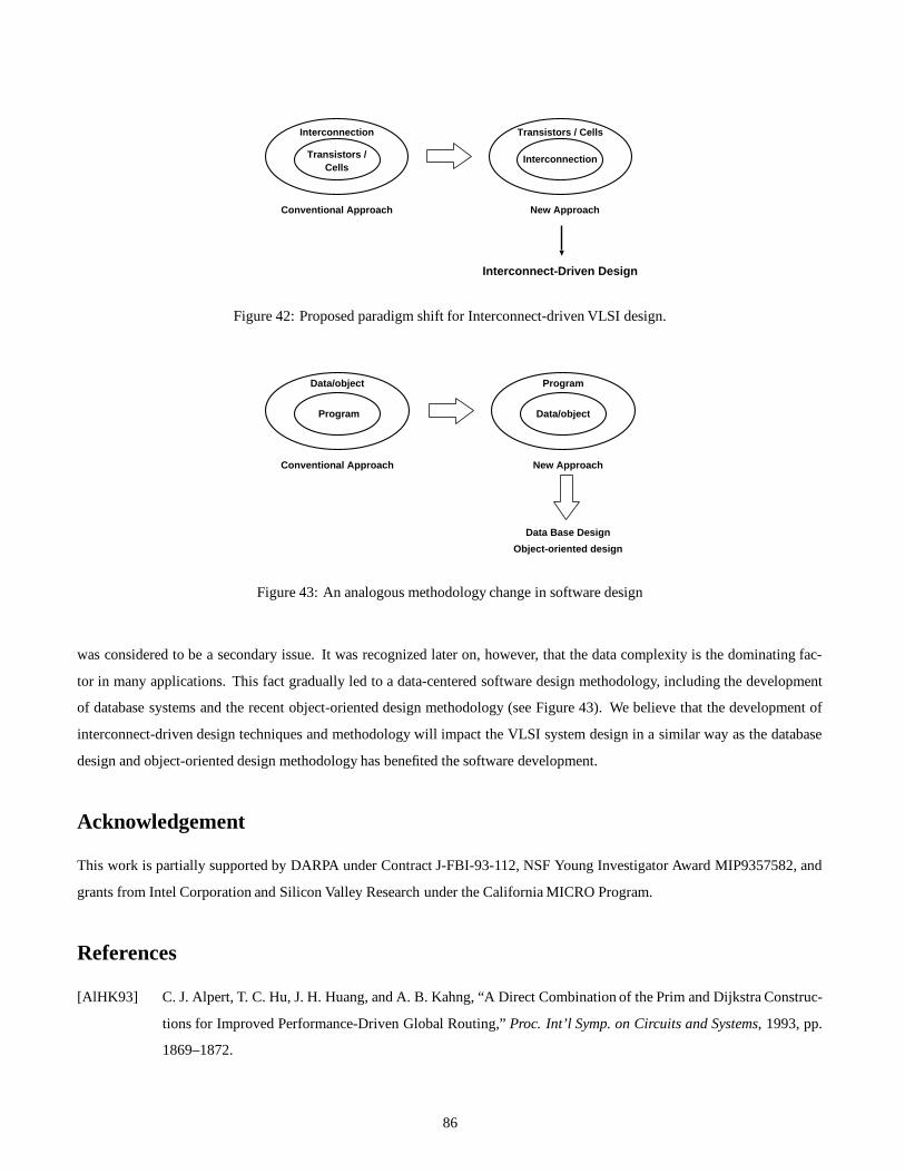
Interconnect-Driven Design
Interconnection
Transistors /Cells
Interconnection
Transistors / Cells
Conventional Approach New Approach
Figure 42: Proposed paradigm shift for Interconnect-driven VLSI design.
Data/object
Program Data/object
Program
Conventional Approach New Approach
Data Base Design
Object-oriented design
Figure 43: An analogous methodology change in software design
was considered to be a secondary issue. It was recognized later on, however, that the data complexity is the dominating fac-
tor in many applications. This fact gradually led to a data-centered software design methodology, including the development
of database systems and the recent object-oriented design methodology (see Figure 43). We believe that the development of
interconnect-driven design techniques and methodology will impact the VLSI system design in a similar way as the database
design and object-oriented design methodology has benefited the software development.
Acknowledgement
This work is partially supported by DARPA under Contract J-FBI-93-112, NSF Young Investigator Award MIP9357582, and
grants from Intel Corporation and Silicon Valley Research under the California MICRO Program.
References
[AlHK93] C. J. Alpert, T. C. Hu, J. H. Huang, and A. B. Kahng, “A Direct Combination of the Prim and Dijkstra Construc-
tions for Improved Performance-Driven Global Routing,” Proc. Int’l Symp. on Circuits and Systems, 1993, pp.
1869–1872.
86
[AwBP90] B. Awerbuch, A. Baratz, and D. Peleg, “Cost-Sensitive Analysis of Communication Protocols,” Proc. ACM Symp.
Principles of Distributed Computing, 1990, pp. 177–187.
[Ba90] H. B. Bakoglu, Circuits, Interconnections, and Packaging for VLSI, Addison-Wesley, 1990.
[BaWM86] H. Bakoglu, J. T. Walker, and J. D. Meindl, “A Symmetric Clock-DistributionTree and Optimized High-Speed In-
terconnections for Reduced Clock Skew in ULSI and WSI Circuits,” Proc. IEEE Int’l Conf. on Computer Design,
Port Chester, 1986, pp. 118–122.
[BeJe90] M. Berkelaar and J. Jess, “Gate Sizing in MOS Digital Circuits with Linear Programming,” Proc. European De-
sign Automation Conf., 1990, pp. 217-221.
[BeBJ94] M. Berkelaar, P. Buurman, and J. Jess, “Computing the Entire Active Area/Power Consumption versus Delay
Trade-off Curve for Gate Sizing with a Piecewise Linear Simulator,” Proc. IEEE Int’l. Conf. on Computer-Aided
Design, 1994, pp. 474-480.
[Be88] M. W. Bern, “Two Probabilistic Results on Rectilinear Steiner Trees,” Algorithmica, 1988, pp. 3:191–204.
[BoKa92] K. D. Boese and A. B. Kahng, “Zero-Skew Clock Routing Trees With Minimum Wirelength,” Proc. IEEE 5th
Int’l ASIC Conf., Rochester, September 1992, pp. 1.1.1 - 1.1.5.
[BoKM93] K. D. Boese, A. B. Kahng, B. A. McCoy, and G. Robins, “Fidelity and Near-Optimality of Elmore-Based Routing
Constructions,” Proc. IEEE Int’l Conf. on Computer Design, October 1993, pp. 81–84.
[BoKM94] K. D. Boese, A. B. Kahng, B. A. McCoy, and G. Robins, “Rectilinear Steiner Trees with Minimum Elmore Delay,”
Proc. Design Automation Conf., 1994, pp. 381–386.
[BoKR93] K. D. Boese, A. B. Kahng, and G. Robins, “High-performance routing trees with identified critical sinks,” Proc.
Design Automation Conf., 1993, pp. 182–187.
[BoKM95] K. D. Boese, A. B. Kahng, B. A. McCoy, and G. Robins, “Near-Optimal Critical Sink Routing Tree Construc-
tions,” IEEE Trans. on Computer-Aided Design, 14(12), Dec. 1995, pp. 1417–1436.
[BoOI94] M. Borah, R. M. Owens, and M. J. Irwin, “An Edge-Based Heuristic for Steiner Routing,” IEEE Trans. on
Computer-Aided Design, 13(12), Dec. 1994, pp. 1563–1568.
[BoOI95] M. Borah, R. M. Owens, and M. J. Irwin, “Transistor Sizing for MinimizingPower Consumptionof CMOS Circuit
under Delay Constraint,” Proc. Int’l Symp. on Lower Power Design, 1995, pp. 167-172.
[BrBK89] F. Brglez, D. Bryan, and K. Kozminski, “Combinational Profiles of Sequential Benchmark Circuits,” Proc. Int’l
Symp. on Circuits and Systems, 1989, pp. 1929–1934.
[CaCh91] R. C. Carden and C.-K. Cheng, “A Global Router Using An Efficient Approximate Multicommodity Multitermi-
nal Flow Algorithm,” Proc. 28th ACM/IEEE Design Automation Conf., 1991, pp. 316–321.
87
[Ch90] P. K. Chan, “Algorithms for Libaray-Specific Sizing of Combinational Logic,” Proc. ACM/IEEE Design Automa-
tion Conf., 1990, pp. 353-356.
[ChHH92a] T.-H. Chao, Y.-C. Hsu, and J.-M. Ho, “Zero Skew Clock Net Routing,” Proc. ACM/IEEE Design Automation
Conf., 1992, pp. 518-523.
[ChHH92b] T.-H. Chao, Y.-C. Hsu, J. M. Ho, K. D. Boese and A. B. Kahng, “Zero Skew Clock Routing With Minimum
Wirelength,” IEEE Trans. on Circuits and Systems, 39(11), Nov. 1992, pp. 799–814.
[ChCW96a] C. P. Chen, Y. W. Chang, and D. F. Wong, “Fast Performance-Driven Optimization for Buffered Clock Trees Based
on Lagrangian Relaxation,” Proc. ACM/IEEE Design Automation Conf., 1996, pp. 405–408.
[ChCW96b] C. P. Chen, Y. P. Chen, and D. F. Wong, “Optimal Wire-Sizing Formula Under the Elmore Delay Model,” Proc.
ACM/IEEE Design Automation Conf., 1996, pp. 487–490.
[ChKa91] H. Y. Chen and S. M. Kang, “iCOACH: A Circuit Optimization Aid for CMOS High-Performance Circuits,”
Integration, the VLSI Journal, vol. 10, Jan. 1991, pp. 155-168.
[ChOK93] K. Chaudhary, A. Onozawa, and E. S. Kuh, “A Spacing Algorithm for Performance Enhancement and Cross-Talk
Reduction,” Proc. IEEE Int’l Conf. on Computer-Aided Design, Nov. 1993, pp. 697–702.
[ChOT95] G. Chen, H. Onodera, and K. Tamaru, “An Iterative Gate Sizing Approach with Accurate Delay Evaluation,”
Proc. IEEE Int’l. Conf. on Computer-Aided Design, 1995, pp. 422-427.
[ChWo96] Y. P. Chen and D. F. Wong, “An Algorithm for Zero-Skew Clock Tree Routing with Buffer Insertion,” Proc. Eu-
ropean Design and Test Conf., 1996.
[ChSa93] J. D. Cho and M. Sarrafzadeh, “A Buffer Distribution Algorithm for High-Speed Clock Routing,” Proc.
ACM/IEEE Design Automation Conf., 1993, pp. 537–543.
[ChCh93] N.-C. Chou and C.-K. Cheng, “Wire Length and Delay Minimization in General Clock Net Routing,” Proc. Int’l
Conf. on Computer-Aided Design, 1993, pp. 552–555.
[ChSa95] W. Chuang and S. S. Sapatnekar, “Power vs. Delay in Gate Sizing: Conflicting Objectives?” Proc. Int’l Conf. on
Computer-Aided Design, November 1995, pp. 463-466.
[ChSH93a] W. Chuang, S. S. Sapatnekar, and I. N. Hajj, “A Unified Algorithm for Gate Sizing and Clock Skew Optimization
to Minimize Sequential Circuit Area,” Proc. Int’l Conf. on Computer-Aided Design, 1993, pp. 220–223.
[ChSH93b] W. Chuang, S. S. Sapatnekar, and I. N. Hajj, “Delay and Area Optimization for Discrete Gate Sizes under Double-
Sided Timing Constraints,” Proc. IEEE Custom Integrated Circuits conf., 1993, pp. 9.4.1-9.4.4.
[ChSH95] W. Chuang, S. S. Sapatnekar, and I. N. Hajj, “Timing and Area Optimization for Standard-Cell VLSI Circuit
Design,” IEEE Trans. on Computer-Aided Design, March 1995, pp. 308-320.
88
[ChCh94] J. Chung and C.-K. Cheng, “Skew Sensitivity Minimization of Buffered Clock Tree,” Proc. Int’l Conf. on
Computer-Aided Design, 1994, pp. 280–283.
[Ci87] M. A. Cirit, “Transistor Sizing in CMOS Circuits,” Proc. 24th ACMIEEE Design Automation Conf., 1987, pp.
121-124.
[CoRa91] J. P. Cohoon and L. J. Randall, “Critical Net Routing,” Proc. Int’l Conf. on Computer Design, 1991, pp. 174–177.
[CoHe95] J. Cong and L. He, “Optimal Wiresizing for Interconnects with Multiple Sources,” Proc. IEEE Int’l. Conf. on
Computer Design, Nov. 1995, pp. 568–574.
[CoHe96a] J. Cong and L. He, “Optimal Wiresizing for Interconnects with Multiple Sources,” ACM Trans. on Design Au-
tomation of Electronic Systems, to appear, 1996 (also available as UCLA Technical Report 95-00031, 1995).
[CoHe96b] J. Cong and L. He, “Simultaneous Transistor and Interconnect Sizing Based on the General Dominance Property”,
Proc. ACM/SIGDA Physical Design Workshop, April. 1996 (also available as UCLA Computer Science, Technical
Report 95-00046).
[CoHe96c] J. Cong and L. He, “An Efficient Approach to Simultaneous Transistor and Interconnect Sizing,” to appear in
Proc. Int’l Conf. on Computer-Aided Design, Nov. 1996.
[CoKK95] J. Cong, A. B. Kahng, C.-K. Koh and C.-W. A. Tsao, “Bounded-Skew Clock and Steiner Routing Under Elmore
Delay,” Proc. Int’l Conf. on Computer-Aided Design, 1995, pp. 66–71.
[CoKR91] J. Cong, A. B. Kahng, and G. Robins, “On Clock Routing for General Cell Layouts,” Proc. IEEE Int’l ASIC Conf.,
Sep. 1991, pp. 14:5.1–14:5.4.
[CoKR91b] J. Cong, A. B. Kahng, G. Robins, M. Sarrafzadeh, and C. K. Wong, “Performance-Driven Global Routing for Cell
Based ICs,” IEEE Int. Conf. Computer Design, 1991, pp. 170–173.
[CoKR93] J. Cong, A. B. Kahng, and G. Robins, “Matching-Based Methods for High-Performance Clock Routing,” IEEE
Trans. on Computer-Aided Design, 12(8), Aug. 1993, pp. 1157–1169.
[CoKR92] J. Cong, A. B. Kahng, G. Robins, M. Sarrafzadeh, and C. K. Wong, “Provably Good Performance-Driven Global
Routing,” IEEE Trans. on Computer-Aided Design, 11(6), June 1992, pp. 739-752.
[CoKL96] J. Cong, C.-K. Koh, and K.-S. Leung, “Simultaneous Buffer and Wire Sizing for Performance and Power Opti-
mization,” Proc. Int’l Symp. on Low Power Electronics and Design, August 1996, pp. 271–276.
[CoKo95] J. Cong and C.-K. Koh, “Minimum-Cost Bounded-Skew Clock Routing,” Proc. IEEE Int’l Symp. on Circuits and
Systems, Apr. 1995, vol. 1, pp. 215–218.
[CoKo94] J. Cong and C.-K. Koh, “Simultaneous Driver and Wire Sizing for Performance and Power Optimization,” IEEE
Trans. on Very Large Scale Integration (VLSI) Systems, 2(4), December 1994, pp. 408-423.
89
[CoLe93] J. Cong and K. S. Leung, “Optimal Wiresizing Under the Distributed Elmore Delay Model,” Proc. Int’l. Conf. on
Computer-Aided Design, 1993, pp. 634-639.
[CoLe95] J. Cong and K. S. Leung, “Optimal Wiresizing Under the Distributed Elmore Delay Model,” IEEE Trans. on
Computer-Aided Design, 14(3), March 1995, pp. 321-336.
[CoLZ93] J. Cong, K. S. Leung, and D. Zhou, “Performance-Driven Interconnect Design Based on Distributed RC Delay
Model,” Proc. ACM/IEEE Design Automation Conf., 1993, pp. 606-611.
[CoMa95] J. Cong and P. H. Madden, “Performance Driven Routing with Multiple Sources,” Proc. Int’l Symp. on Circuits
and Systems, 1995, pp. 1157–1169.
[CoMa95b] J. Cong and P. H. Madden, “Performance Driven Routing with Multiple Sources,” Tech. Rep. CSD-950002,
UCLA, Jan. 1995.
[CoPr88] J. Cong and B. Preas, “A New Algorithm for Standard Cell Global Routing,” Proc. IEEE Int’l Conf. on Computer-
Aided Design, Nov. 1988, pp. 176–179.
[DaAs89] Z. Dai and K. Asada, “MOSIZ: A Two-Step Transistor Sizing Algorithm Based on Optimal Timing Assignment
Method for Multi-stage Complex Gates, ” Proc. 1989 Custom Integrated Circuits Conf., pp. 17. 3. 1-17. 3. 4, May
1989.
[DaKJ90] W. M. Dai, R. Kong, J. Jue, and M. Sato, “Rubber Band Routing and Dynamic Data Representation,” Proc. Int’l
Conf. on Computer-Aided Design, Nov. 1990, pp. 52–55.
[DaMQ94] F. Dartu, N. Menezes, J. Qian, and L. T. Pillage, “A Gate-Delay Model for High-Speed CMOS Circuits,” Proc.
ACM/IEEE Design Automation Conf., 1994, pp. 576-580.
[DeCJ96] M. P. Desai, R. Cvijetic, and J. Jensen, “Sizing of Clock DistributionNetworks for High Performance CPU Chips,”
Proc. 33rd Design Automation Conf., 1996, pp. 389–394.
[DhFW84] S. Dhar, M. A. Franklin, and D. F. Wann, “Reduction of Clock Delays in VLSI Structures,” Proc. Int’l Conf. on
Computer Design, 1984, pp. 778–783.
[Di59] E. Dijkstra, “A Note on Two Problems in Connexion with Graphs,” Numerische Mathematik, 1959, pp. 1:269–
271.
[DrWa72] S. E. Dreyfus and R. A. Wagner, “The Steiner Problem in Graphs,” Networks, I:195–207, 1972.
[Ec80] J. G. Ecker, “Geometric Programming: Methods, Computations and Applications,” SIAM Review, vol. 22, No. 3,
July 1980, pp. 338-362.
[Ed91] M. Edahiro, “Minimum Skew and Minimum Path Length Routing in VLSI Layout Design,” NEC Research and
Development, 32(4), Oct. 1991, pp. 569–575.
90
[Ed92] M. Edahiro, “Minimum Path-Length Equi-Distant Routing,” Proc. IEEE Asia-Pacific Conf. on Circuits and Sys-
tems, Dec. 1992, pp. 41–46.
[Ed93a] M. Edahiro, “A Clustering-Based Optimization Algorithm in Zero-Skew Routing,” Proc. ACM/IEEE Design Au-
tomation Conf., Jun. 1993, pp. 612–616.
[Ed93b] M. Edahiro, “Delay Minimization for Zero-Skew Routing,” Proc. IEEE Int’l Conf. on Computer-Aided Design,
1993, pp. 563-566.
[Ed94] M. Edahiro, “An Efficient Zero-Skew Routing Algorithm,” Proc. ACM/IEEE Design Automation Conf., Jun.
1994, pp. 375–380.
[El48] W. C. Elmore, “The Transient Response of Damped Linear Networks with Particular Regard to Wide-Band Am-
plifiers,” Journal of Applied Physics, vol. 19, no. 1, Jan. 1948, pp. 55–63.
[Fi90] J. P. Fishburn, “Clock Skew Optimization,” IEEE Trans. on Computers, 39(7), Jul. 1990, pp. 945–951.
[FiDu85] J. P. Fishburn and A. E. Dunlop, “TILOS: A Posynomial Programming Approach to Transistor Sizing,” Proc.
Int’l. Conf. on Computer-Aided Design, 1985, pp. 326-328.
[FiKu82] A. L. Fisher and and H. T. Kung, “Synchronizing Large Systolic Arrays,” Proc. SPIE, vol. 341, May 1982, pp.
44-52.
[Fr92a] J. Frankle, “Iterative and Adaptive Slack Allocation for Performance-Driven Layout and FPGA Routing,” Proc.
ACM/IEEE Design Automation Conf., 1992, pp. 536–542.
[Fr92b] E. G. Friedman, “The Application of Localized Clock Distribution Design to Improving the Performance of Re-
timed Sequential Circuits,” Proc. of IEEE Asia-Pacific Conf. on Circuits and Systems, Dec 1992, pp. 12–17.
[Fr95] E. G. Friedman, Editor, Clock Distribution networks in VLSI Circuits and Systems: A Selected Reprint Volume,
1995.
[GaLi93] T. Gao and C. L. Liu, “Minimum Crosstalk Channel Routing,” Proc. IEEE Int’l Conf. on Computer-Aided Design,
Nov. 1993, pp. 692–696.
[GaLi94] T. Gao and C. L. Liu, “Minimum Crosstalk Switchbox Routing,” Proc. IEEE Int’l Conf. on Computer-Aided De-
sign, Nov. 1994, pp. 610–615.
[GaZh93] D. S. Gao and D. Zhou, “Propagation Delay in RLC Interconnection Networks,” Proc. IEEE Int’l Symp. on Cir-
cuits and Systems, 1993, pp. 2125–2128.
[GaJo79] M. R. Garey and D. S. Johnson, Computers and Intractability, W. H. Freeman, San Francisco, 1979.
[GePa87] G. Georgakopoulos and C. H. Papadimitriou, “The 1-Steiner Tree Problem,” Journal of Algorithms, vol. 8, 1987,
pp. 122-130.
91
[GuTK95] R. Gupta, B. Tutuianu, B. Krauter, and L. T. Pillage, “The Elmore Delay as a Bound for RC Trees with Generalized
Input Signals,” Proc. 32nd ACM/IEEE Design Automation Conf., June 1995, pp. 364–369.
[Ha66] M. Hanan, “On Steiner’s Problem with Rectilinear Distance,” SIAM Journal of Applied Mathematics, 14, 1966,
pp. 255–265.
[HeJe87] N. Hedenstierna and K. O. Jeppson, “CMOS Circuit Speed and Buffer Optimization,” IEEE Trans. on Computer-
Aided Design, 1987, pp. 270-281.
[He87] K. S. Hedlund, “AESOP: A Tool for Automatic Transistor Sizing,” Proc. 24 ACMIEEE Design AutomationConf.,
1987, pp. 114-120.
[HeFi91] L. S. Heulser and W. Fichtner, “Transistor Sizing for Large Combinational Digital CMOS Circuits,” Integration,
the VLSI Journal, vol. 10, Jan. 1991, pp. 185-212.
[HiKo92] U. Hinsberger and R. Kolla, “A Cell-based Approach to Performance Optimization of Fanout-Free Circuits,”
IEEE Trans. on Computer-Aided Design, vol. 11, No. 10, Oct., 1992, pp. 1317-1321.
[HLCW89] J.-M. Ho, D. T. Lee, C.-H. Chang, and C. K. Wong. “Bounded-Diameter Minimum Spanning Trees and Related
Problems,” Proc. Computational Geometry Conf., 1989, pp. 276–282.
[HoVW90] J. M. Ho, G. Vijayan, and C. K. Wong. “New Algorithms for the Rectilinear Steiner Tree Problem,” IEEE Trans.
on Computer-Aided Design, 9(2), 1990, pp. 185–193.
[HoMR94] T. D. Hodes, B. A. McCoy, and G. Robins, “Dynamically-Wiresized Elmore-Based Routing Constructions,”
Proc. Int’l Symp. on Circuits and Systems, 1994, pp. 463-466.
[HoNS90] B. Hoppe, G. Neuendore, D. Schmitt-Landsiedel, and W. Specks “Optimization of High-Speed CMOS Logic
Circuits with Analytical Models for Signal Delay, Chip Area and Dynamic Power Dissipation,” IEEE Trans. on
Computer-Aided Design, 9(3), March 1990, pp. 237-247.
[Ho84] M. A. Horowitz, “Timing Models for MOS Circuits,” PhD Thesis, Stanford University, January, 1984.
[HoXK93] X. Hong, T. Xue, E. S. Kuh, C. K. Cheng, and J. Huang, “Performance-Driven Steiner Tree Algorithms For Global
Routing,” Proc. ACM/IEEE Design Automation Conf., 1993, pp. 177-181.
[HuKT95] J. H. Huang, A. B. Kahng and C.-W. A. Tsao, “On the Bounded-Skew Routing Tree Problem,” Proc. ACM/IEEE
Design Automation Conf., San Francisco, Jun. 1995, pp. 508-513.
[Hw76] F. K. Hwang, “On Steiner Minimal Trees with Rectilinear Distance,” SIAM Journal of Applied Mathematics,
30(1), Jan. 1976, pp. 104–114.
[HwRi92] F. K. Hwang and D. S. Richards, “Steiner Tree Problems,” Networks, 22:55–89, 1992.
[JaSK90] M. A. B. Jackson, A. Srinivasan and E. S. Kuh, “Clock Routing for High Performance ICs,” Proc. ACM/IEEE
Design Automation Conf., 1990, pp. 573–579.
92
[KaCR91] A. B. Kahng, J. Cong and G. Robins, “High-Performance Clock Routing Based on Recursive Geometric Match-
ing,” Proc. ACM/IEEE Design Automation conf., June 1991, pp. 322-327.
[KaMM96] A. B. Kahng, K. Masuko, and S. Muddu, “Analytical Delay Model for VLSI Interconnects Under Ramp Input”,
UCLA CS Dept. TR-960015, April 1996, also to appear in Proc. Int’l Conf. on Computer-Aided Design, Nov.
1996.
[KaMu94] A. B. Kahng and S. Muddu, “Optimal Equivalent Circuits for Interconnect Delay Calculations Using Moments,”
Proc. European Design Automation Conf., Sep. 1994, pp. 164–169.
[KaMu95] A. B. Kahng and S. Muddu, “Two-pole Analysis of Interconnection Trees”, Proc. IEEE Multi-ChipModule Conf.,
January 1995, pp. 105–110.
[KaMu96a] A. B. Kahng and S. Muddu, “Efficient Gate Delay Modeling for Large Interconnect Loads,” Proc. IEEE Multi-
Chip Module Conf., 1996, pp. 202–207.
[KaMu96b] A. B. Kahng and S. Muddu, “Accurate Analytical Delay Models fo r VLSI Interconnects”, IEEE Int. Symposium
on Circuits and Systems, May 1996.
[KaRo92] A. B. Kahng and G. Robins, “A New Class of Iterative Steiner Tree Heuristics with Good Performance,” Trans.
on Computer-Aided Design, 11(7), July 1992, pp. 893–902,
[KaRo94] A. B. Kahng and G. Robins, On Optimal Interconnections for VLSI, Kluwer Academic Publishers, 1994.
[KaSS90] K. Kawamura, T. Shindo, T. Shibuya, H. Miwatari, and Y. Ohki, “Touch and Cross Router,” Proc. IEEE Int’l
Conf. on Computer-Aided Design, Nov. 1990, pp. 56–59.
[KaTs94a] A. B. Kahng and C.-W. A. Tsao, “Planar-DME: Improved Planar Zero-Skew Clock Routing with Minimum Path-
length Delay,” Proc. European Design Automation Conf., 1994, pp. 440-445.
[KaTs94b] A. B. Kahng and C.-W. A. Tsao, “Low-Cost Single-Layer Clock Trees with Exact Zero Elmore Delay Skew,”
Proc. IEEE Int’l Conf. on Computer-Aided Design, 1994, pp. 213–218.
[KhCo95] K. Y. Khoo and J. Cong, “An Efficient Multilayer MCM Router Based on Four-Via Routing,” IEEE Trans. on
Computer-Aided Design, Oct. 1995, pp. 1277-1290.
[KhRY93] S. Khuller, B. Raghavachari, and N. Young. “Balancing Minimum Spanning Trees and Shortest-Path Trees,” Proc.
Symp. on Discrete Algorithms, 1993, pp. 243–250.
[KiSa94] D. A. Kirkpatrick and A. L. Sangiovanni-Vincentelli, “Techniques for Crosstalk Avoidance in the Physical Design
of High-Performance Digital Systems,” Proc. IEEE Int’l Conf. on Computer-Aided Design, Nov. 1994, pp. 616–
619.
[KrGW95] B. Krauter, R. Gupta, J. Willis, and L. T. Pileggi, “Transmission Line Synthesis,” Proc. 32nd ACM/IEEE Design
Automation Conf., June 1995, pp. 358–363.
93
[Kr56] J. B. Kruskal, “On the Shortest Spanning Subtree of a Graph,” Proc. American Math Society, vol. 7, 1956, pp.
48–50.
[KuGa82] S. Y. Kung and R. J. Gal-Ezer, “Synchronous vs Asynchronous Computation in VLSI Array Processor,” Proc.
SPIE, vol. 341, May 1982, pp. 53–65.
[LeSe88] K.-W. Lee and C. Sechen, “A New Global Router for Row-Based Layout,” Proc. IEEE Int’l Conf. on Computer-
Aided Design, Nov. 1988, pp. 180–183.
[LeWo80] D. T. Lee and C. K. Wong, “Voronoi Diagrams in l1 (l∞) Metrics with 2-Dimensional Storage Applications,” SIAM
Journal of Computation, vol. 9, No. 1, February 1980, pp. 200–211.
[Li94] W. Li, “Strongly NP-hard Discrete Gate-Size Problems,” IEEE Trans. on Computer-Aided Design, vol. 13, No.
8, Aug. 1994, pp. 1045-1051.
[LiLA92] W. Li, A. Lim, P. Agrawal, and S. Sahni, and R. Kolla, “On the Circuit Implementation Problem,” Proc.
ACM/IEEE Design Automation Conf., 1992, pp. 478-483.
[LiDW93] H. Liao, W. Dai, R. Wang, and F. Y. Chang, “S-Parameter Based Macro Model of Distributed-Lumped Networks
Using Exponentially Decayed Polynomial Function,” Proc. 30th ACM/IEEE Design Automation Conf., 1993, pp.
726–731.
[LiCL95] J. Lillis, C. K. Cheng and T. T. Y. Lin, “Optimal Wire Sizing and Buffer Insertion for Low Power and a Generalized
Delay Model,” Proc. IEEE Int’l. Conf. on Computer-Aided Design, Nov. 1995, pp. 138-143.
[LiCL96a] J. Lillis, C. K. Cheng and T. T. Y. Lin, “Simultaneous Routing and Buffer Insertion for High Performance Inter-
connect,” Proc. the Sixth Great Lakes Symp. on VLSI, 1996.
[LiCL96b] J. Lillis, C. K. Cheng, T. T. Y. Lin, and C. Y. Ho, “New Performance Driven Routing Techniques With Explicit
Area/Delay Tradeoff and Simultaneous Wire Sizing,” Proc. ACM/IEEE Design Automation Conf., June 1996, pp.
395-400.
[LiCW93] A. Lim, S.-W. Cheng, and C.-T. Wu. “Performance Oriented Rectilinear Steiner Trees,” Proc. ACM/IEEE Design
Automation Conf., 1993, pp. 171–175.
[LiHT89] Y.-L. Lin, Y.-C. Hsu, and F.-S. Tsai, “SILK: A Simulated Evolution Router,” IEEE Trans. on Computer-Aided
Design, 8(10), Oct. 1989, pp. 1108–1114.
[LiLi75] H. C. Lin, L. W. Linholm, “An Optimized OutputStage for MOS Integrated Circuits,” IEEE Journal of Solid-State
Circuits, SC-10(2), 1975, pp. 106-109.
[LiMK90] S. Lin, M. Marek-Sadowska, and E. S. Kuh, “Delay and Area Optimization in Standard-cell Design,” Proc.
ACM/IEEE Design Automation Conf., 1990, pp. 349-352.
94
[LiWo94] S. Lin and C. K. Wong, “Process-Variation-Tolerant Clock Skew Minimization,” Proc. Int’l Conf. on Computer-
Aided Design, 1994, pp. 284–288.
[Ma86] D. P. Marple, “Transistor Size Optimizationof DigitalVLSI Circuits,” Tech. Rep. CSL-TR-86-308, Stanford Univ.,
Oct. 1986.
[Ma63] D. W. Marquardt, “An Algorithm for Least-Squares Estimation of Nonlinear Parameters,” SIAM Journal of Ap-
plied Mathematics, vol. 11, 1963, pp. 431–441.
[Ma93] A. Martinez, “Timing Model Accuracy Issues and Automated Library Characterization,” IFIP Transactions A
(Computer Science and Technology), vol. A-22, 1993, pp. 413–426.
[MeCo93] C. Mead and L. Conway, Introduction to VLSI Systems, Addison-Wesley, 1993.
[MeBP95] N. Menezes, R. Baldick, and L. T. Pileggi, “A Sequential Quadratic Programming Approach to Concurrent Gate
and Wire Sizing,” Proc. Int’l Conf. on Computer-Aided Design, 1995, pp. 144-151.
[MePD94] N. Menezes, S. Pullela, F. Dartu and L. T. Pillage, “RC Interconnect Synthesis —- A Moment Fitting Approach,”
Proc. Int’l Conf. on Computer-Aided Design, 1994, pp. 418-425.
[MePP93] N. Menezes, A. Balivada, S. Pullela, and L. T. Pillage, “Skew Reduction in Clock Trees Using Wire Width Opti-
mization,” Proc. IEEE Custom Integrated Circuits Conf., 1993, pp. 9.6.1–9.6.4.
[MePP95] N. Menezes, S. Pullela, and L. T. Pileggi, “Simultaneous Gate and Interconnect Sizing for Circuit-Level Delay
Optimization,” Proc. 32nd ACM/IEEE Design Automation Conf., June 1995, pp. 690–695.
[Mi90] M. Minoux, “Efficient Greedy Heuristics for Steiner Tree Problems Using Reoptimization and Supermodularity,”
INFOR, 28(3), Aug. 1990, pp. 221-233.
[Na75] L. W. Nagel, “SPICE2: A Computer Program to Simulate Semiconductor Circuits,” Technical Report ERL-M520,
UC-Berkeley, May 1975.
[NaBH89] R. Nair, L. Berman, P. S. Hauge, and E. J. Yoffa, “Generation of Performance Constraints for Layout,” IEEE
Trans. on Computer-Aided Design, 8(8), 1989, pp. 860–874.
[NeFr93] J. L. Neves and E. G. Friedman, “Topological Design of Clock Distribution Networks Based on Non-Zero Clock
Skew Specifications,” Proc of 36th Midwest Symp. on Circuits and Systems, Aug. 1993, pp. 468–471.
[NeFr94] J. L. Neves and E. G. Friedman, “Circuit Synthesis of Clock Distribution Networks Based on Non-Zero Clock
Skew,” Proc of IEEE Int’l Symp. on circuits and Systems, June 1994, pp. 4.175–4.178.
[NeFr95] J. L. Neves and E. G. Friedman, “Minimizing Power Dissipation in Non-Zero Skew-based Clock Distribution
Networks,” Proc of IEEE Int’l Symp. on Circuits and Systems, Apr. 1995, pp. 3.1577–3.1579.
[OkCo96a] T. Okamoto and J. Cong, “Interconnect Layout Optimization by Simultaneous Steiner Tree Construction and
Buffer Insertion,” Proc. ACM/SIGDA Physical Design Workshop, April. 1996, pp. 1–6.
95
[OkCo96b] T. Okamoto and J. Cong, “Buffered Steiner Tree Construction with Wire Sizing for Interconnect Layout Opti-
mization,” to appear in Proc. Int’l Conf. on Computer-Aided Design, Nov. 1996.
[OBSa89] P. R. O’Brien and T. L. Savarino, “Modeling the Driving-Point Characteristic of Resistive Interconnect for Ac-
curate Delay Estimation,” Proc. Int’l Conf. on Computer-Aided Design, Nov. 1989, pp. 512–515.
[OhPP96] J. Oh, I. Pyo and M. Pedram, “Constructing Lower and Upper Bounded Delay Routing Trees Using Linear Pro-
gramming,” Proc. 33rd Design Automation Conf., 1996, pp. 401–404.
[Ou84] J. K. Ousterhout, “Switch-Level Delay Models for Digital MOS VLSI,” Proc. 21st Design Automation Conf.,
1984, pp. 542–548.
[Po78] M. J. D. Powell, “A Fast Algorithmfor Nonlinear ConstrainedOptimization Calculations,” Lecture Notes in Math-
ematics, no. 630, ed. G. A. Watson, Springer Verlag, 1978, pp. 144-157.
[Pi95] L. Pileggi, “Coping with RC(L) Interconnect Design Headaches,” Proc. Int’l Conf. on Computer-Aided Design,
Nov. 1995, pp. 246–253.
[PiRo90] L. T. Pillage and R. A. Rohrer, “Asymptotic Waveform Evaluation for Timing Analysis,” IEEE Trans. on
Computer-Aided Design, 9(4), Apr. 1990, pp. 352–366.
[PiSk72] D. J. Pilling and J. G. Skalnik, “A Circuit Model for Predicting Transient Delays in LSI Logic Systems,” Proc.
6th Asilomar Conf. on Circuits and Systems, 1972, pp. 424–428.
[PrKu90] S. Prasitjutrakul and W. J. Kubitz, “A Timing-Driven Global Router for Custom Chip Design,” Proc. Int’l Conf.
on Computer-Aided Design, 1990, pp. 48-51.
[Pr57] R. C. Prim, “Shortest Connecting Networks,” Bell System Technical Journal, vol. 31, 1957, pp. 1398–1401.
[PuMO93] S. Pullela, N. Menezes, J. Omar and L. Pillage, “Skew and Delay Optimization for Reliable Buffered Clock
Trees,” Proc. IEEE Int’l Conf. on Computer-Aided Design, 1993, pp. 556–562.
[PuMP93] S. Pullela, N. Menezes and L. T. Pillage, “Reliable Non-Zero Skew Clock Tree Using Wire Width Optimization,”
Proc. ACM/IEEE Design Automation Conf., 1993, pp. 165-170.
[QiPP94] J. Qian, S. Pullela, and L. T. Pileggi, “Modeling the “Effective Capacitance” for the RC Interconnect of CMOS
Gates,” IEEE Trans. on Computer-Aided Design of Integrated Circuits and Systems, 13(12), Dec. 1994, pp. 1526–
1535.
[RaSh89] P. Ramanathan and K. G. Shin, “A Clock Distribution Scheme for Non-Symmetric VLSI Circuits,” Proc. Int’l
Conf. on Computer-Aided Design, 1989, pp. 398–401.
[RaSH92] S. K. Rao, P. Sadayappan, F. K. Hwang, and P. W. Shor, “The Rectilinear Steiner Arboresence Problem,” Algo-
rithmica, 1992, pp. 277–288.
96
[RaPi94] C. L. Ratzlaff and L. T. Pillage, “RICE: Rapid Interconnect Circuit Evaluation Using AWE,” IEEE Trans. on
Computer-Aided Design of Integrated Circuits and Systems, 13(6), June 1994, pp. 763–776.
[RuPH83] J. Rubinstein, P. Penfield, Jr., and M. A. Horowitz, “Signal Delay in RC Tree Networks,” IEEE Trans. on
Computer-Aided Design, CAD-2(3), July 1983, pp. 202–211.
[Sa83] T. Sakurai, “Approximation of Wiring Delay in MOS-FET LSI,” IEEE Journal of Solid-State Circuits, vol. 4,
1983, pp. 418–426.
[SaSa94] P. K. Sancheti and S. S. Sapatnekar, “Interconnect Design Using Convex Optimization,” Proc. IEEE Custom In-
tegrated Circuits Conf., 1994, pp. 549-552.
[Sa94] S. S. Sapatnekar, “RC Interconnect Optimization Under the Elmore Delay Model,” Proc. ACM/IEEE Design Au-
tomation Conf., 1994, pp. 387-391.
[Sap90] S. S. Sapatnekar and V. B. Rao, “iDEAS: A Delay Estimator and Transistor Sizing Tool for CMOS Circuits,”
Proc. IEEE Custom Integrated Circuits Conf., May 1990, pp. 9. 3. 1-9. 3. 4.
[SeIK94] M. Seki, K. Inoue, K. Kato, K. Tsurusaki, S. Fukasawa, H. Sasaki, and M. Aizawa, “A Specified Delay Accom-
plishingClock Router Using Multiple Layers,” Proc. IEEE Int’l Conf. on Computer-Aided Design, 1994, pp. 289–
292.
[SIA94] Semiconductor Industry Association, National Technology Roadmap for Semiconductors, 1994.
[SaRV93] S. S. Sapatnekar, V. B. Rao, P. M. Vaidya, and S. M. Kang, “An Exact Solution to the Transistor Sizing Problem
for CMOS Circuits Using Convex Optimization,” IEEE Trans. on Computer-Aided Design, November 1993, pp.
1621-1634.
[SaSF95] H. Sathyamurthy, S. S. Sapatnekar and J. P. Fishburn, “Speeding up Pipelined Circuits through a Combination of
Gate Sizing and Clock Skew Optimization,” Proc. Int’l Conf. on Computer-Aided Design, 1995, pp. 467–470.
[ShFD88] J. Shyu, J. P. Fishburn, A. E. Dunlop, and A. L. Sangiovanni-Vincentelli, “Optimization Based Transistor Sizing,”
IEEE Journal of Solid-State Circuits, pp. 400-409, Apr. 1988.
[SmLi79] J. M. Smith and J. S. Liebman. “Steiner Trees, Steiner Circuits and the Interference Problem in Building Design,”
Engineering Optimization, 30(4), 1979, pp. 15–36.
[SoFr94] T. Soyata and E. G. Friedman, “Retiming with Non-Zero Clock Skew, Variable Register, and Interconnect Delay,”
Proc. Int’l Conf. on Computer-Aided Design, Nov 1994, pp. 234–241.
[SoFM95] T. Soyata, E. G. Friedman, and J. H. Mulligan, Jr., “Monotonicity Constraints on Path Delays for Efficient Retim-
ing with Localized Clock Skew and Variable Register Delay,” Proc. of IEEE Int’l Symp. on Circuits and Systems,
Apr. 1995, pp. 3.1748–3.1751.
[SrKa94] M. Sriram and S. K. Kang, Physical Design for Multichip Modules, Kluwer Academic Publishers, 1994.
97
[TaMF94] Y. Tamiya, Y. Matsunaga, and M. Fujita, “LP Based Cell Selection with Constraints of Timing, Area and Power
Consumption,” Proc. Int’l Conf. on Computer-Aided Design, Nov. 1994, pp. 378–381.
[TeKS96] G. E. Tellez, D. Knol, and M. Sarrafzadeh, “A Graph-Based Delay Budgeting Algorithm for Large Scale Timing-
Driven Placement Problem,” Proc. 5th ACM/SIGDA Physical Design Workshop, April 1996, pp. 234–240.
[TeSa94] G. E. Tellez and M. Sarrafzadeh, “Clock Period Constrained Minimal Buffer Insertion in Clock Trees,” Proc. Int’l
Conf. on Computer-Aided Design, Nov. 1994, pp. 219–223.
[TeFS95] G. E. Tellez, Amir Farrahi, and M. Sarrafzadeh, “Activity-Driven Clock Design for Low Power Circuits,” Proc.
IEEE Int’l Conf. on Computer-Aided Design, Nov. 1995, pp. 62–65.
[Ts91] R. S. Tsay, “Exact Zero Skew,” Proc. Int’l Conf. on Computer-Aided Design, 1991, pp. 336-339.
[TuDP96] B. Tutuianu, F. Dartu, and L. Pileggi, “An Explicit RC-Circuit Delay Approximation Based on the First Three
Moments of the Impulse Response,” Proc. 33rd Design Automation Conf., 1996, pp. 611–616.
[va90] L. P. P. P. van Ginneken, “Buffer Placement in Distributed RC-tree Networks for Minimal Elmore Delay,” Proc.
Int’l Symp. on Circuits and Systems, 1990, pp. 865-868.
[Va89] P. M. Vaidya, “A New Algorithm for Minimizing Convex Functions over Convex Set,” Proc. IEEE Foundations
of Computer Science, Oct. 1989, pp. 338-343.
[Ve84] H. J. M. Veendrick, “Short-Circuit Dissipation of Static CMOS Circuitry and Its Impact on the Design of Buffer
Circuits,” IEEE Journal of Solid-State Circuits, SC-19(4), August 1984, pp. 468-473.
[ViMa94] A. Vittal and M. Marek-Sadowska, “Minimal Delay Interconnect Design Using Alphabetic Trees,” Proc.
ACM/IEEE Design Automation Conf., San Diego, June 1994, pp. 392–396.
[ViMa95] A. Vittal and M. Marek-Sadowska, “Power Optimal Buffered Clock Tree Design,” Proc. ACM/IEEE Design Au-
tomation Conf., San Francisco, June 1995, pp. 497–502.
[WaFr83] D. F. Wann and M. A. Franklin, “Asynchronous and Clocked Control Structures for VLSI Based Interconnection
Networks,” IEEE Trans. on Computer, C-32(3), March 1983, pp. 284–293.
[WeEs93] N. H. E. Weste and K. Eshraghian, Principles of CMOS VLSI Design: a Systems Perspective – 2nd ed, Addison-
Wesley, 1993.
[WuSh92] B. Wu and N. A. Sherwani, “Effective Buffer Insertion of Clock Tree for High-Speed VLSI Circuits,” Microelec-
tronics Journal, vol. 23, 1992, pp. 291–300.
[Wy87] J. L. Wyatt, Circuit Analysis, Simulation and Design – Part 2, Chapter 11, North-Holland, 1987.
[XiDa95] J. G. Xi and W. W.-M. Dai, “Buffer Insertion and Sizing Under Process Variations for Low Power Clock Distri-
bution,” Proc. ACM/IEEE Design Automation Conf., 1995, pp. 491–496.
98
[XiDa96] J. G. Xi and W. W.-M. Dai, “Useful-Skew Clock Routing with Gate Sizing for Low Power Design,” Proc. 33rd
Design Automation Conf., 1996, pp. 383–388.
[XuKu95a] T. Xue and E. S. Kuh, “Post RoutingPerformance Optimization via Tapered Link Insertion and Wiresizing,” Proc.
European Design Automation Conf., 1995.
[XuKu95b] T. Xue and E. S. Kuh, “Post Routing Performance Optimization via Multi-Link Insertion and Non-Uniform Wire-
sizing,” Proc. Int’l Conf. on Computer-Aided Design, 1995, pp. 575–580.
[XuKW96] T. Xue, E. S. Kuh, and D. Wang, “Post Global Routing Crosstalk Risk Estimation and Reduction,” to appear in
Proc. IEEE Int’l Conf. on Computer-Aided Design, Nov. 1996.
[XuKY96] T. Xue, E. S. Kuh and Q. Yu, “A Sensitivity-Based Wiresizing Approach to Interconnect OPtimization of Lossy
Transmission Line Topologies,” Proc. IEEE Multi-Chip Module Conf., 1996, pp. 117-121.
[YuKu95a] Q. Yu and E. S. Kuh “Moment Models of General Transmission Line with Application to MCM Interconnect
Analysis,” Proc. IEEE Multi-Chip Module Conf., 1995, pp. 594-598.
[YuKu95b] Q. Yu and E. S. Kuh “Exact Moment Matching Model of Transmission Lines and Application to Interconnect
Delay Estimation,” IEEE Trans. on Very Large Scale Integration (VLSI) Systems, 3(2), Jun. 1995, pp. 311–322.
[ZhLi96] D. Zhou, and X. Y. Liu, “On the Optimal Drivers for High-Speed Low Power ICs,” to appear in International
Journal of High Speed Electronics and System, 1996.
[ZhST93] D. Zhou, S. Su, F. Tsui, D. S. Gao, and J. S. Cong, “A Two-Pole Circuit Model for VLSI High-Speed Intercon-
nection,” Proc. IEEE Int’l Symp. on Circuits and Systems, 1993, pp. 2129–2132.
[ZhST94] D. Zhou, S. Su, F. Tsui, D. S. Gao, and J. S. Cong, “A Simplified synthesis of Transmission Lines with A Tree
Structure,” Int’l Journal of Analog Integrated Circuits and Signal Processing, Jan. 1994, pp. 19–30.
[ZhTG93] D. Zhou, F. Tsui, and D. S. Gao, “High Performance Multichip Interconnection Design,” Proc. 4th ACM/SIGDA
Physical Design Workshop, Apr. 1993, pp. 32–43.
[ZhDa92] Q. Zhu and W. W.-M. Dai, “Perfect-balance planar clock routing with minimal path-length,” Proc. Int’l Conf. on
Computer-Aided Design, 1992, pp. 473–476.
[ZhDX93] Q. Zhu, W. W.-M. Dai, and J. G. Xi, “Optimal Sizing of High-Speed Clock Networks Based on Distributed RC
and Lossy Transmission Line Models,” Proc. Int’l Conf. on Computer-Aided Design, 1993, pp. 628–633.
[ZhXDS94] Q. Zhu, J. G. Xi, W. W.-M. Dai, and R. Shukla, “Low Power Clock Distribution Based on Area Pad Interconnect
for Multichip Modules,” Proc. Int’l Workshop of Low Power Design, 1994, pp. 87–92.
99