Embed Size (px)
Citation preview
PERFORMANCE AND POWER OPTIMIZATION IN VLSI PHYSICAL DESIGN
A Thesis
by
ZHANYUAN JIANG
Submitted to the Office of Graduate Studies ofTexas A&M University
in partial fulfillment of the requirements for the degree of
MASTER OF SCIENCE
December 2007
Major Subject: Computer Engineering
PERFORMANCE AND POWER OPTIMIZATION IN VLSI PHYSICAL DESIGN
A Thesis
by
ZHANYUAN JIANG
Submitted to the Office of Graduate Studies ofTexas A&M University
in partial fulfillment of the requirements for the degree of
MASTER OF SCIENCE
Approved by:
Chair of Committee, Weiping ShiCommittee Members, Jiang Hu
Donald K. Friesen
Head of Department, Costas N. Georghiades
December 2007
Major Subject: Computer Engineering

iii
ABSTRACT
Performance and Power Optimization in VLSI Physical Design. (December 2007)
Zhanyuan Jiang, B.S., Shanghai Jiao Tong University
Chair of Advisory Committee: Dr. Weiping Shi
As VLSI technology enters the nanoscale regime, a great amount of efforts have
been made to reduce interconnect delay. Among them, buffer insertion stands out
as an effective technique for timing optimization. A dramatic rise in on-chip buffer
density has been witnessed. For example, in two recent IBM ASIC designs, 25% gates
are buffers.
In this thesis, three buffer insertion algorithms are presented for the procedure
of performance and power optimization. The second chapter focuses on improv-
ing circuit performance under inductance effect. The new algorithm works under
the dynamic programming framework and runs in provably linear time for multiple
buffer types due to two novel techniques: restrictive cost bucketing and efficient delay
update. The experimental results demonstrate that our linear time algorithm con-
sistently outperforms all known RLC buffering algorithms in terms of both solution
quality and runtime. That is, the new algorithm uses fewer buffers, runs in shorter
time and the buffered tree has better timing.
The third chapter presents a method to guarantee a high fidelity signal trans-
mission in global bus. It proposes a new redundant via insertion technique to reduce
via variation and signal distortion in twisted differential line. In addition, a new
buffer insertion technique is proposed to synchronize the transmitted signals, thus
further improving the effectiveness of the twisted differential line. Experimental re-
iv
sults demonstrate a 6GHz signal can be transmitted with high fidelity using the new
approaches. In contrast, only a 100MHz signal can be reliably transmitted using a
single-end bus with power/ground shielding. Compared to conventional twisted dif-
ferential line structure, our new techniques can reduce the magnitude of noise by 45%
as witnessed in our simulation.
The fourth chapter proposes a buffer insertion and gate sizing algorithm for
million plus gates. The algorithm takes a combinational circuit as input instead of
individual nets and greatly reduces the buffer and gate cost of the entire circuit.
The algorithm has two main features: 1) A circuit partition technique based on the
criticality of the primary inputs, which provides the scalability for the algorithm, and
2) A linear programming formulation of non-linear delay versus cost tradeoff, which
formulates the simultaneous buffer insertion and gate sizing into linear programming
problem. Experimental results on ISCAS85 circuits show that even without the circuit
partition technique, the new algorithm achieves 17X speedup compared with path
based algorithm. In the meantime, the new algorithm saves 16.0% buffer cost, 4.9%
gate cost, 5.8% total cost and results in less circuit delay.

v
To My parents and Lihua
vi
ACKNOWLEDGMENTS
I would like to express my sincere gratitude to my advisor Professor Weiping Shi.
Professor Shi led me into the world of VLSI design automation. I truly appreciate all
his academic and financial support. With the help of Professor Shi, I not only gained
profound knowledge in academics, but also learned the scientific attitude towards
research. I am also very thankful for all his advice for my career and life, as well as
for his constant encouragement and friendship.
Many thanks to my other committee members, Professor Jiang Hu and Professor
Donald Friesen. I appreciate very much their invaluable assistance.
Many thanks to Professor Jiang Hu for his inspiring courses in VLSI design, which
provided me with many techniques for VLSI circuit analysis and optimization. In his
course projects, I implemented several algorithms and performed a lot of simulations,
which prepared me well to be confident in my job interview.
Many thanks to Professor Donald Friesen for introducing me to the algorithm
world, which provided me a solid foundation for my research. Before his course, I
knew little about algorithm analysis and design. I am very grateful to having taken
his course in the beginning of my graduate life.
Special thanks to my friends and fellow graduate students. Thanks to Shiyan Hu
for his help with my research work and writing. I learned a lot in daily discussions
with him, from coding style to paper writing. Thanks to Zhuo Li for his advice on my
research work. He is a model of diligence and intelligence, encouraging me to make
progress in my work. Thanks to Cheng-Ta Chiang for introducing me to Latex and
many useful hints on that. Thanks to Yang Yi, Zhuo Feng, Xiaoji Ye, Guo Yu, Wei
Dong, Weihuang Wang and Yifang Liu for making computer engineering group a big
family and a wonderful place to work.
vii
I wish to thank my parents for their encouragement, support and truly believing
in me.
Thanks to my wife Lihua Han. Without her support and belief in my work, I
could not imagine this thesis being accomplished.
viii
TABLE OF CONTENTS
CHAPTER Page
I INTRODUCTION . . . . . . . . . . . . . . . . . . . . . . . . . . 1
A. Technology Trend . . . . . . . . . . . . . . . . . . . . . . . 1
B. Contribution . . . . . . . . . . . . . . . . . . . . . . . . . . 3
C. Organization . . . . . . . . . . . . . . . . . . . . . . . . . . 4
II AN RLC BUFFER INSERTION ALGORITHM . . . . . . . . . 5
A. Introduction . . . . . . . . . . . . . . . . . . . . . . . . . . 5
B. Delay Model . . . . . . . . . . . . . . . . . . . . . . . . . . 7
1. Inductance Impact on Delay . . . . . . . . . . . . . . 7
2. Interconnect Delay Model . . . . . . . . . . . . . . . . 8
3. CMOS Gate Delay Model . . . . . . . . . . . . . . . . 12
C. RLC Buffering Algorithm . . . . . . . . . . . . . . . . . . 13
1. Preliminaries . . . . . . . . . . . . . . . . . . . . . . . 13
2. Overview of van Ginneken’s Algorithm . . . . . . . . . 13
3. Algorithm . . . . . . . . . . . . . . . . . . . . . . . . . 15
a. Sink . . . . . . . . . . . . . . . . . . . . . . . . . 17
b. Wire Insertion . . . . . . . . . . . . . . . . . . . . 17
c. Buffer Insertion . . . . . . . . . . . . . . . . . . . 18
d. Branch Merge . . . . . . . . . . . . . . . . . . . . 19
e. Linear Time Complexity . . . . . . . . . . . . . . 19
D. Experimental Results . . . . . . . . . . . . . . . . . . . . . 21
1. Comparison between Ismail and NEW . . . . . . . . . 22
2. Comparison between van Ginneken-Lillis, Impedance
and NEW+COST . . . . . . . . . . . . . . . . . . . . 22
III A TWISTED DIFFERENTIAL LINE FOR GLOBAL BUS . . . 24
A. Introduction . . . . . . . . . . . . . . . . . . . . . . . . . . 24
B. Effect of Via Variation . . . . . . . . . . . . . . . . . . . . 26
1. Experiments Setup . . . . . . . . . . . . . . . . . . . . 26
2. Single-end Bus Structure . . . . . . . . . . . . . . . . 26
3. Standard Twisted Differential Line Structure . . . . . 28
C. New Twisted Differential Line Structure . . . . . . . . . . 31
1. Redundant Via Insertion . . . . . . . . . . . . . . . . 32

ix
CHAPTER Page
2. Buffer Insertion . . . . . . . . . . . . . . . . . . . . . 35
IV CIRCUIT-WISE BUFFER INSERTION AND GATE SIZ-
ING ALGORITHM WITH SCALABILITY . . . . . . . . . . . . 37
A. Introduction . . . . . . . . . . . . . . . . . . . . . . . . . . 37
B. Problem Formulation . . . . . . . . . . . . . . . . . . . . . 39
C. Algorithm . . . . . . . . . . . . . . . . . . . . . . . . . . . 40
1. Post-buffering Timing Estimation . . . . . . . . . . . 42
2. Circuit Partition Technique . . . . . . . . . . . . . . . 43
a. The Partition Boundary . . . . . . . . . . . . . . 44
b. Side Inputs and Outputs . . . . . . . . . . . . . . 45
3. Linear Formulation of Delay vs. Cost Tradeoff . . . . 45
4. Linear Programming . . . . . . . . . . . . . . . . . . . 49
a. LP Formulation . . . . . . . . . . . . . . . . . . . 50
b. Redundant Variables and Constraints Removal . . 50
5. Considering Slew and Buffer Congestion . . . . . . . . 52
D. Experimental Results . . . . . . . . . . . . . . . . . . . . . 53
1. Comparison between Path Based and Circuit-wise
Algorithms . . . . . . . . . . . . . . . . . . . . . . . . 53
2. The Effect of the Partition Technique . . . . . . . . . 56
3. Testcase with Million Plus Gates . . . . . . . . . . . . 56
V CONCLUSION AND FUTURE WORK . . . . . . . . . . . . . . 58
A. Conclusion . . . . . . . . . . . . . . . . . . . . . . . . . . . 58
B. Future Work . . . . . . . . . . . . . . . . . . . . . . . . . . 59
REFERENCES . . . . . . . . . . . . . . . . . . . . . . . . . . . . . . . . . . . 60
VITA . . . . . . . . . . . . . . . . . . . . . . . . . . . . . . . . . . . . . . . . 65
x
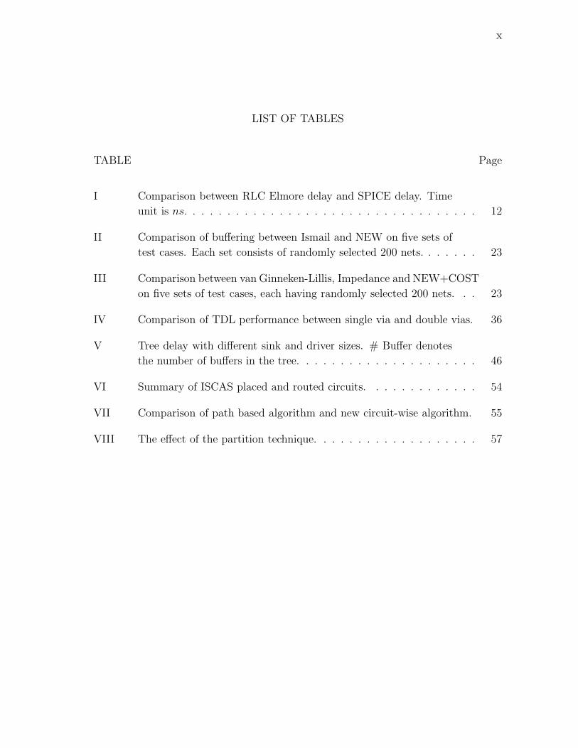
LIST OF TABLES
TABLE Page
I Comparison between RLC Elmore delay and SPICE delay. Time
unit is ns. . . . . . . . . . . . . . . . . . . . . . . . . . . . . . . . . . 12
II Comparison of buffering between Ismail and NEW on five sets of
test cases. Each set consists of randomly selected 200 nets. . . . . . . 23
III Comparison between van Ginneken-Lillis, Impedance and NEW+COST
on five sets of test cases, each having randomly selected 200 nets. . . 23
IV Comparison of TDL performance between single via and double vias. 36
V Tree delay with different sink and driver sizes. # Buffer denotes
the number of buffers in the tree. . . . . . . . . . . . . . . . . . . . . 46
VI Summary of ISCAS placed and routed circuits. . . . . . . . . . . . . 54
VII Comparison of path based algorithm and new circuit-wise algorithm. 55
VIII The effect of the partition technique. . . . . . . . . . . . . . . . . . . 57

xi
LIST OF FIGURES
FIGURE Page
1 Percentage of nets requiring buffers. M3 and M6 represent nets
on third and sixth metal layer in a six metal layer technology. . . . . 2
2 Buffers as a percentage of the total cell count for the chip. . . . . . . 3
3 Capacitance crosstalk path of a signal line. . . . . . . . . . . . . . . . 7
4 Comparison of output signals between RLC and RC in global wires. . 9
5 Comparison of output signals between RLC and RC in interme-
diate wires. . . . . . . . . . . . . . . . . . . . . . . . . . . . . . . . . 9
6 A single segment of an RLC circuit. . . . . . . . . . . . . . . . . . . 10
7 An RLC tree. . . . . . . . . . . . . . . . . . . . . . . . . . . . . . . . 11
8 The data structure of cost buckets . . . . . . . . . . . . . . . . . . . 16
9 Time complexity of new RLC algorithm with respect to the num-
ber of buffer positions. . . . . . . . . . . . . . . . . . . . . . . . . . . 20
10 A single-end model of 8-bit global bus. OP denotes the signal
observation point. . . . . . . . . . . . . . . . . . . . . . . . . . . . . 27
11 (a) Noise signal is measured at OP in Figure 10. The peak noise of
6GHz input signal is 0.35V. (b) The peak noise of 200MHz input
signal is 0.18V, of 100MHz is 0.15V and of 50MHz is 0.11V. . . . . . 27
12 A TDL structure of 8-bit global bus with single via. . . . . . . . . . . 29
13 (a) Signal in TDL structure with single via and without variation.
Output signal is measured at OP4 in Figure 12. (b) Signal in TDL
structure with single via and with via variation. Output signal is
measured at OP4 in Figure 12. . . . . . . . . . . . . . . . . . . . . . 29
xii
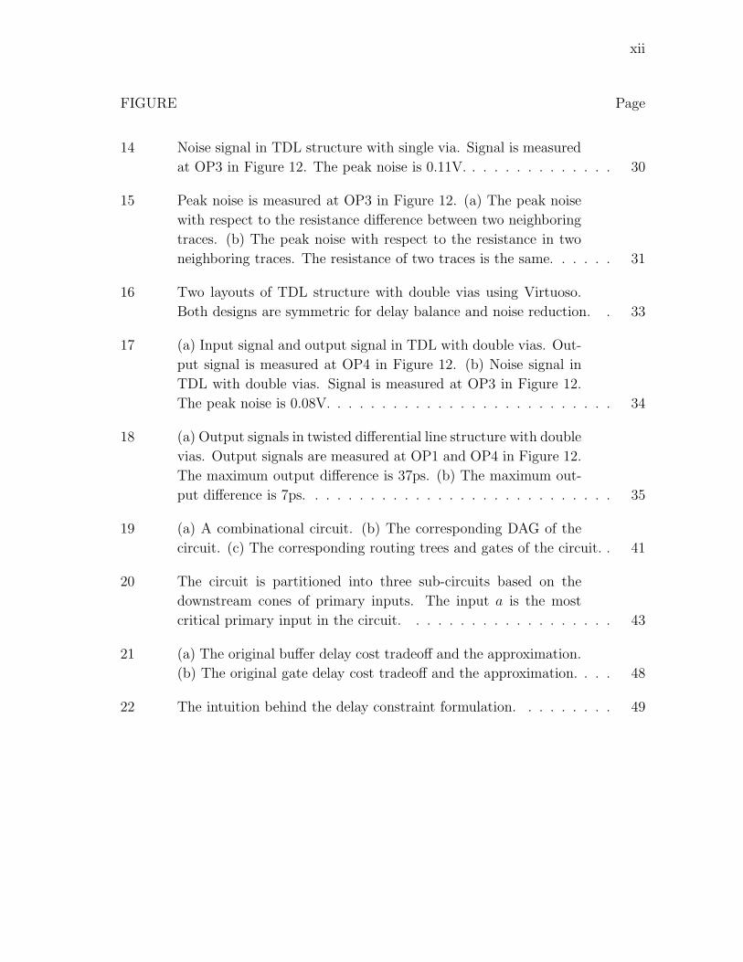
FIGURE Page
14 Noise signal in TDL structure with single via. Signal is measured
at OP3 in Figure 12. The peak noise is 0.11V. . . . . . . . . . . . . . 30
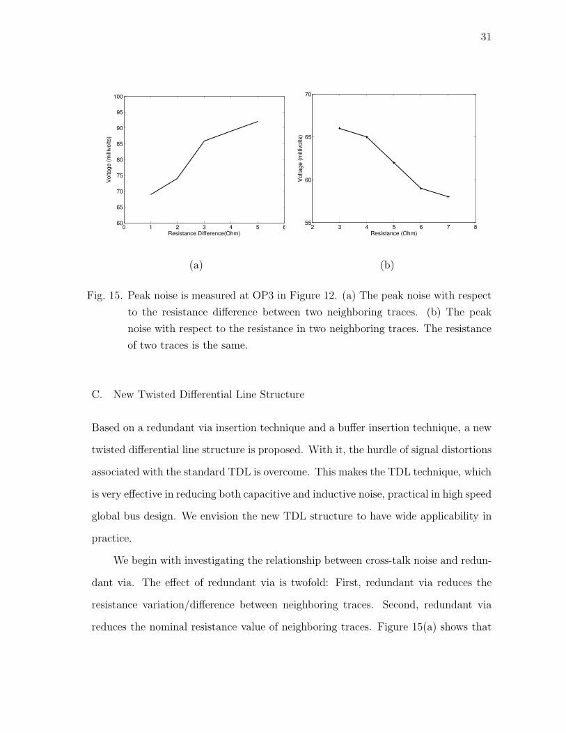
15 Peak noise is measured at OP3 in Figure 12. (a) The peak noise
with respect to the resistance difference between two neighboring
traces. (b) The peak noise with respect to the resistance in two
neighboring traces. The resistance of two traces is the same. . . . . . 31
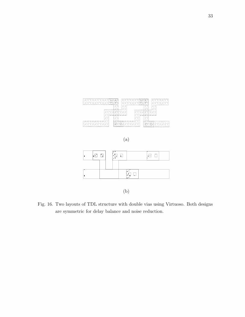
16 Two layouts of TDL structure with double vias using Virtuoso.
Both designs are symmetric for delay balance and noise reduction. . 33
17 (a) Input signal and output signal in TDL with double vias. Out-
put signal is measured at OP4 in Figure 12. (b) Noise signal in
TDL with double vias. Signal is measured at OP3 in Figure 12.
The peak noise is 0.08V. . . . . . . . . . . . . . . . . . . . . . . . . . 34
18 (a) Output signals in twisted differential line structure with double
vias. Output signals are measured at OP1 and OP4 in Figure 12.
The maximum output difference is 37ps. (b) The maximum out-
put difference is 7ps. . . . . . . . . . . . . . . . . . . . . . . . . . . . 35
19 (a) A combinational circuit. (b) The corresponding DAG of the
circuit. (c) The corresponding routing trees and gates of the circuit. . 41
20 The circuit is partitioned into three sub-circuits based on the
downstream cones of primary inputs. The input a is the most
critical primary input in the circuit. . . . . . . . . . . . . . . . . . . 43
21 (a) The original buffer delay cost tradeoff and the approximation.
(b) The original gate delay cost tradeoff and the approximation. . . . 48
22 The intuition behind the delay constraint formulation. . . . . . . . . 49

1
CHAPTER I
INTRODUCTION
A. Technology Trend
As the continuous trend of Very Large Scale Integration (VLSI) circuits technology
scaling and frequency increasing, interconnect delay becomes a significant bottleneck
in system performances. This trend is a result of increased resistance of the inter-
connect when feature sizes enter the nano-meter era. From International Technology
Roadmap for Semiconductors (ITRS) projection, interconnect delay can contribute to
more than 50% of the delay when the feature size is beyond 180 nm. As a result, de-
lay optimization techniques for interconnect are increasingly important for achieving
timing closure of high performance designs. A great effort has been made to reduce
interconnect delay and buffer insertion appears as a very effective technique.
The objective of buffer insertion is to find where to insert buffers in the intercon-
nect so that the timing requirements are met. Since the propagation Elmore delay
has a square dependence on the length of an RC interconnect line, subdividing the
line into shorter sections is an effective strategy to reduce the total propagation de-
lay. The interconnect can be subdivided into shorter sections by inserting repeaters,
which breaks the quadratic dependence of the delay on the interconnect length but
adds additional parasitic impedances due to the inserted repeaters. Thus, an opti-
mum number and size of repeaters exist that minimizes the total propagation delay
of the line [1, 2].
Owing to the tremendous drop in VLSI feature size, a huge number of buffers
are needed for achieving timing objectives for interconnects. It is stated in a recent
The journal model is IEEE Transactions on Automatic Control.

2
0
5
10
15
20
25
30
35
90nm 65nm 45nm 32nm
Technology node
% b
uff
ere
d n
ets
M3
M6
Fig. 1. Percentage of nets requiring buffers. M3 and M6 represent nets on third and
sixth metal layer in a six metal layer technology.
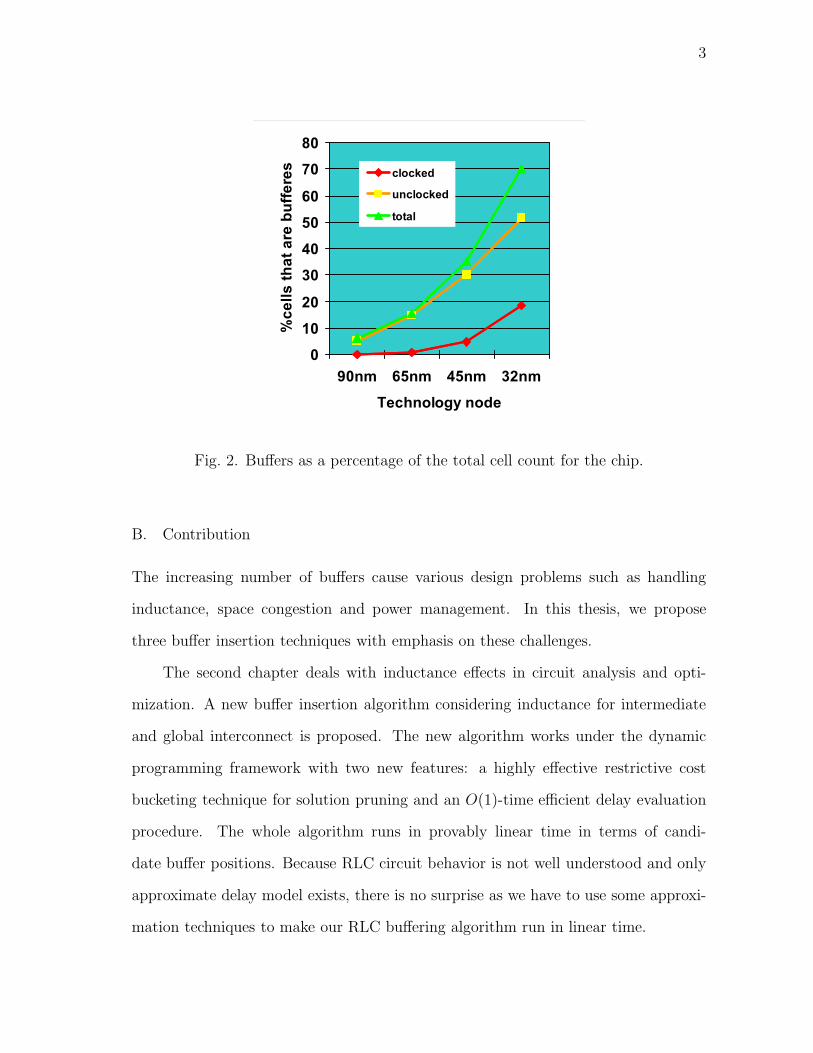
study [3] that the number of nets that need buffer insertion and the number of buffers
will rise dramatically. For example, 12% of nets require buffer insertion and the
number of buffers (including clocked buffers) reaches about 15% of the total cell
count for intrablock communications for 65nm technology. At 32nm technology node,
these numbers become 29% and 70% respectively. The trend is shown in Figure 1 and
Figure 2. Although we are not sure whether the number of 70% will finally be reached,
hundreds of thousands of buffers can be found in todays ASICs. For example, Osler [4]
presents an existing chip with 426 thousand buffers which occupy 15% of the available
area. From Figure 1 and Figure 2, the rate at which the percentage of impacted nets
is increasing and the rate at which the percentage of buffers is increasing both start
accelerating. Therefore, both the complexity and importance of buffer insertion is
increasing in an even faster pace.
3
0
10
20
30
40
50
60
70
80
90nm 65nm 45nm 32nm
Technology node
%c
ell
s t
ha
t a
re b
uff
ere
s
clocked
unclocked
total
Fig. 2. Buffers as a percentage of the total cell count for the chip.
B. Contribution
The increasing number of buffers cause various design problems such as handling
inductance, space congestion and power management. In this thesis, we propose
three buffer insertion techniques with emphasis on these challenges.
The second chapter deals with inductance effects in circuit analysis and opti-
mization. A new buffer insertion algorithm considering inductance for intermediate
and global interconnect is proposed. The new algorithm works under the dynamic
programming framework with two new features: a highly effective restrictive cost
bucketing technique for solution pruning and an O(1)-time efficient delay evaluation
procedure. The whole algorithm runs in provably linear time in terms of candi-
date buffer positions. Because RLC circuit behavior is not well understood and only
approximate delay model exists, there is no surprise as we have to use some approxi-
mation techniques to make our RLC buffering algorithm run in linear time.

4
The third chapter focuses on reducing signal distortion and synchronizing the
transmitted signals, which improves the effectiveness of the twisted differential line
in global bus design. A new redundant via insertion technique is proposed to reduce
via resistance variation, and then a new buffer technique with spacing constraint is
proposed to synchronize the output signals.
The fourth chapter proposes a buffer insertion and gate sizing algorithm for
million plus gates. The algorithm takes combinational circuit as input instead of
individual nets, which greatly reduces the buffer cost and gate cost of the entire circuit.
The algorithm has two main features: 1) A circuit partition technique based on the
criticality of the primary inputs, which provides the scalability for the algorithm, and
2) A linear programming formulation of non-linear delay versus cost tradeoff, which
formulates the simultaneous buffer insertion and gate sizing into linear programming
problem.
C. Organization
This thesis is organized as follows. In Chapter II, we introduce the most classical
work in buffer insertion and the buffer insertion algorithm considering inductance. In
Chapter III, a new twisted differential line structure in global bus design is proposed.
In Chapter IV, we present circuit-wise buffer insertion and gate sizing algorithm with
scalability. Finally, conclusion and future work are presented in Chapter V.
5
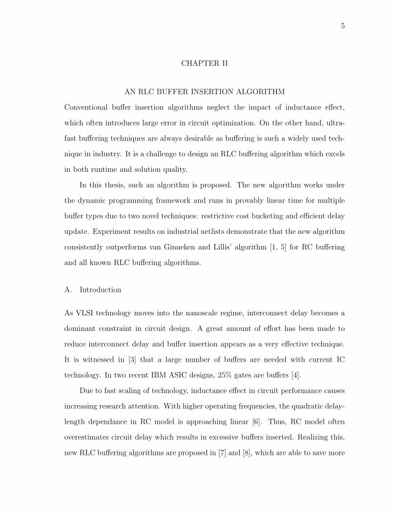
CHAPTER II
AN RLC BUFFER INSERTION ALGORITHM
Conventional buffer insertion algorithms neglect the impact of inductance effect,
which often introduces large error in circuit optimization. On the other hand, ultra-
fast buffering techniques are always desirable as buffering is such a widely used tech-
nique in industry. It is a challenge to design an RLC buffering algorithm which excels
in both runtime and solution quality.
In this thesis, such an algorithm is proposed. The new algorithm works under
the dynamic programming framework and runs in provably linear time for multiple
buffer types due to two novel techniques: restrictive cost bucketing and efficient delay
update. Experiment results on industrial netlists demonstrate that the new algorithm
consistently outperforms van Ginneken and Lillis’ algorithm [1, 5] for RC buffering
and all known RLC buffering algorithms.
A. Introduction
As VLSI technology moves into the nanoscale regime, interconnect delay becomes a
dominant constraint in circuit design. A great amount of effort has been made to
reduce interconnect delay and buffer insertion appears as a very effective technique.
It is witnessed in [3] that a large number of buffers are needed with current IC
technology. In two recent IBM ASIC designs, 25% gates are buffers [4].
Due to fast scaling of technology, inductance effect in circuit performance causes
increasing research attention. With higher operating frequencies, the quadratic delay-
length dependance in RC model is approaching linear [6]. Thus, RC model often
overestimates circuit delay which results in excessive buffers inserted. Realizing this,
new RLC buffering algorithms are proposed in [7] and [8], which are able to save more
6
than 30% buffers compared to the minimum cost RC buffering algorithms.
In [7], a top-down greedy style RLC algorithm is proposed. At each candidate
buffer position, the delay at a driver is evaluated to decide whether a buffer is inserted.
This method gives a great reduction of the buffer area. Due to the top-down nature
of the algorithm, a tree traversal is needed to collect RLC information for delay
evaluation, which is the bottleneck for the efficiency of the algorithm. Since only
a single solution is maintained, this algorithm still runs fast, however, it sacrifices
solution quality.
In [8], a different RLC algorithm based on dynamic programming is designed.
The main contributions of [8] are the concept of downstream impedance and new
pruning condition to speed up the solution propagation. However, the approach is
not efficient. Experimental results in [8] show that the algorithm runs significantly
slower than RC timing buffering algorithms. In reality, buffering techniques are often
applied to huge volume of nets and thus fast buffering techniques are highly desired.
This imposes great challenge on designing state-of-the-art buffer insertion algorithm
and motivates this work.
In this thesis, we propose the fastest RLC buffer insertion algorithm. The new
algorithm works under the dynamic programming framework with two new features:
a highly effective restrictive cost bucketing technique for solution pruning and an
O(1)-time efficient delay evaluation procedure. The whole algorithm runs in provably
linear time in terms of candidate buffer positions. Because RLC circuit behavior is not
well understood and only approximate delay model exists, there is no surprise as we
have to use some approximation techniques to make our RLC buffering algorithm run
in linear time. The experimental results demonstrate that our linear time algorithm
consistently outperforms all known RLC buffering algorithms in terms of both solution
quality and runtime. That is, the new algorithm uses fewer buffers, runs in shorter
7
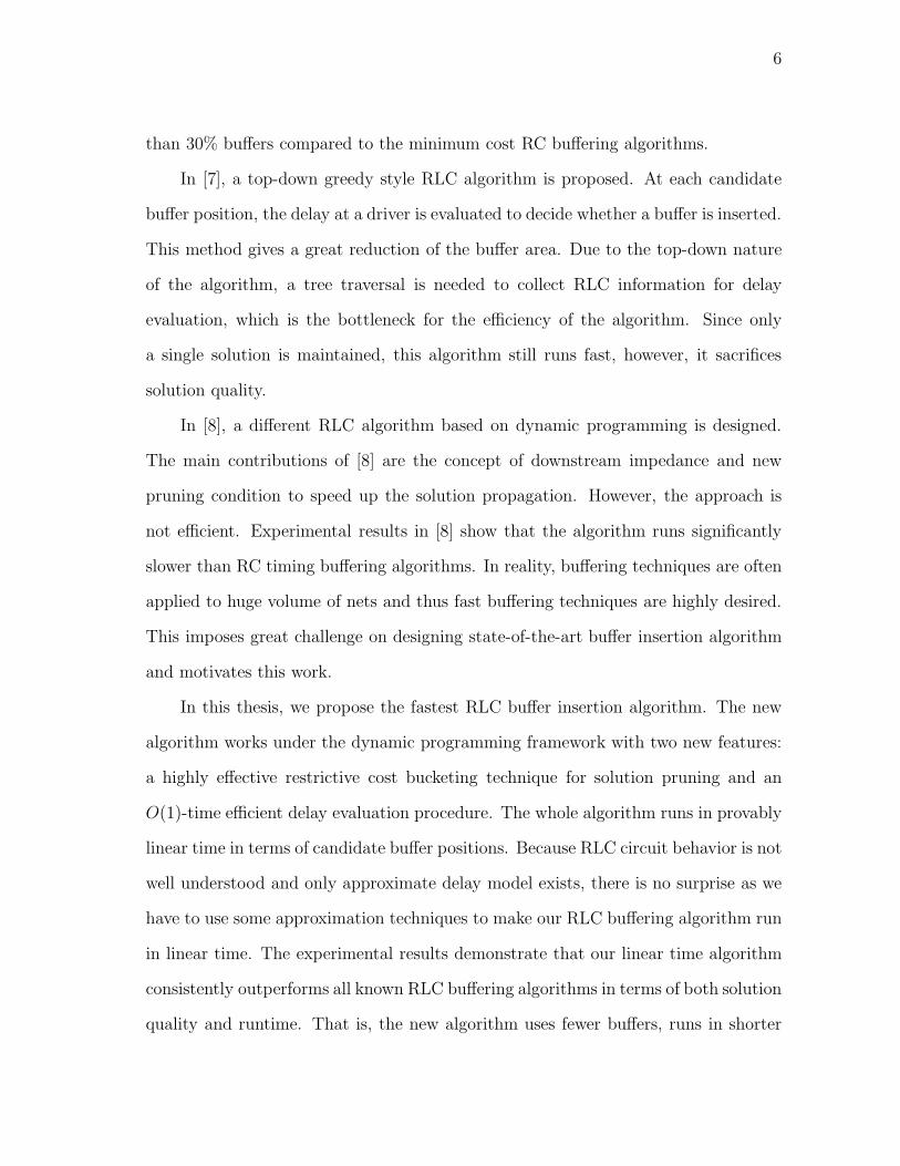
Fig. 3. Capacitance crosstalk path of a signal line.
time and the buffered tree has better timing. In particular, the new algorithm gives
up to 8.5% buffer saving and 4× speedup over [7]. When buffer cost minimization is
handled, 5.3% fewer buffers and 5× speedup is obtained over [8].
B. Delay Model
Since the prevailing RC Elmore delay model does not catch the actual performance
considering inductance effect, various authors claim 30% to 100% timing errors [6, 9].
Thus, more accurate delay models are necessary for accurate timing analysis and
buffer insertion. Such a model will be introduced in this section.
1. Inductance Impact on Delay
To accurately investigate the inductance impact on delay, it is important to have
the realistic range of unit parasitic resistance, capacitance and inductance. We set
8
up a realistic environment to accurately extract the parasitics based on the model
of [10]. Since the inductance effect depends on current return path, the capacitance
crosstalk path which is shown in Figure 3 is crucial. The signal line is assumed to have
two neighboring lines which remain static during the entire analysis period. Then,
FastCap [11] and FastHenry [12] are used to extract capacitance and inductance. For
MOSIS 130nm technology [13], the following parameters are obtained. From metal
layer one to six, unit resistance varies from 350Ω/mm to 10Ω/mm, unit capacitance
from 380fF/mm to 180fF/mm and unit inductance from 0.6nH/mm to 1.3nH/mm.
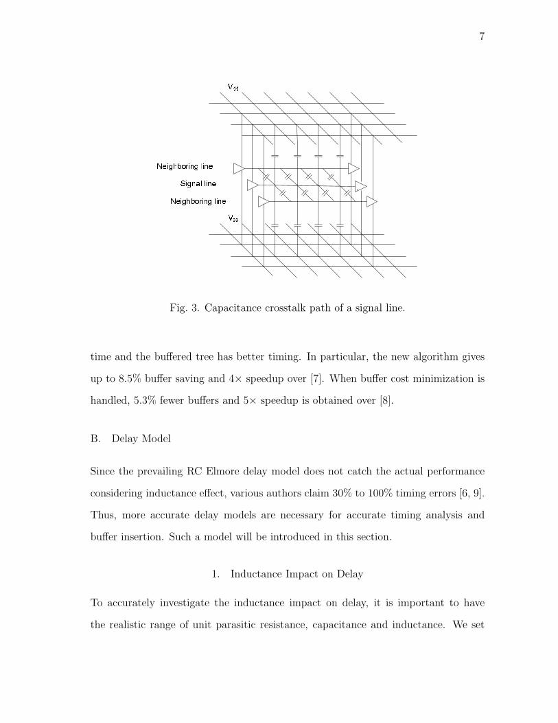
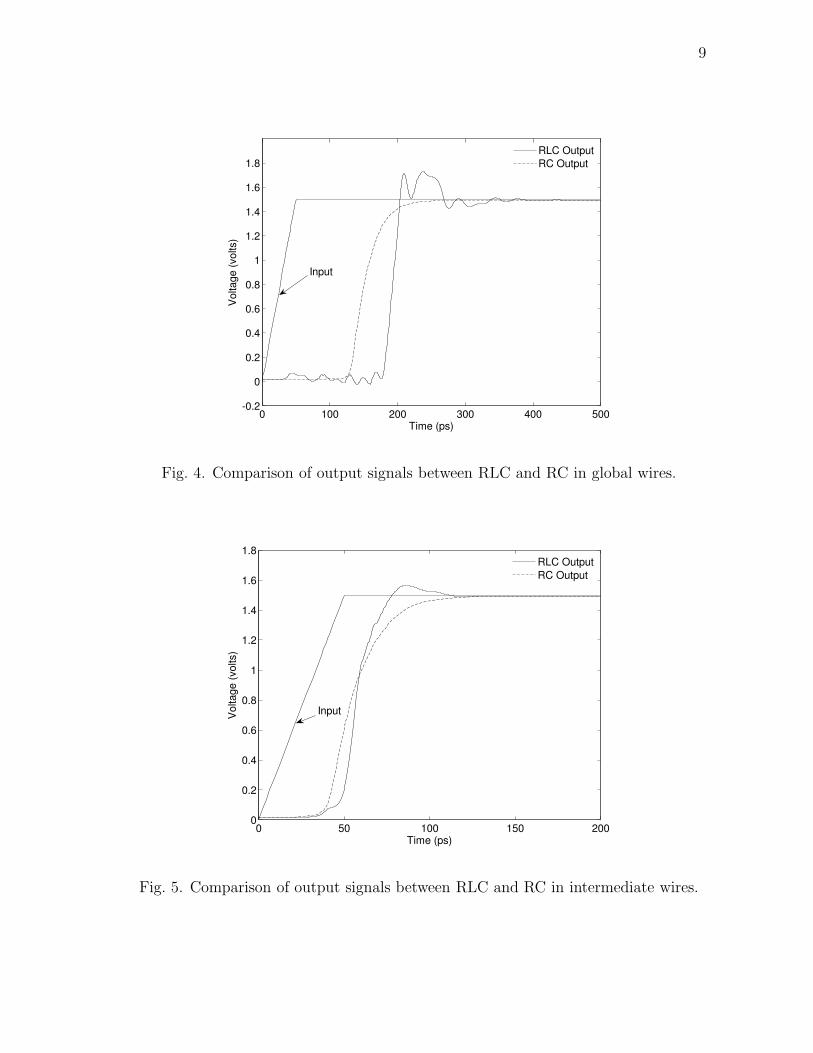
We investigated inductance effect in global wires and intermediate wires both.
SPICE simulation results demonstrate that differences between applications of RLC
model and RC model to global wires on metal layer five and six (Figure 4) and
intermediate wires on metal layer three and four (Figure 5) are quite significant.
The inductance introduces 20% additional delay to global wires and also causes large
overshoot, while relatively less impact has been observed on intermediate wires. The
reason behind this phenomenon is that unit resistance of global wires is much less
than that of intermediate wires.
2. Interconnect Delay Model
An equivalent Elmore delay model of an RLC tree from [14] is adopted in this thesis.
The model comes from a second order approximation of transfer function, which
preserves the same accuracy for RLC trees as that of Elmore delay with respect to
RC trees.
A single line segment of an RLC circuit is shown in Figure 6. This circuit has a
second order transfer function which is given by
h(s) =ω2
n
s2 + s2ζωn + ω2n
, (2.1)
9
0 100 200 300 400 500-0.2
0
0.2
0.4
0.6
0.8
1
1.2
1.4
1.6
1.8
Time (ps)
Voltage (
volts)
RLC Output
RC Output
Input
Fig. 4. Comparison of output signals between RLC and RC in global wires.
0 50 100 150 2000
0.2
0.4
0.6
0.8
1
1.2
1.4
1.6
1.8
Time (ps)
Voltage (
volts)
RLC Output
RC Output
Input
Fig. 5. Comparison of output signals between RLC and RC in intermediate wires.

10
Fig. 6. A single segment of an RLC circuit.
where
ζ =1
2
RC√LC
and ωn =1√LC
. (2.2)
For a general RLC tree shown in Figure 7, the voltage drop at node Ni compared
with the input voltage is
Vin(s) − Vi(s) =∑
k
CkVk(s)s(Rki + Lkis), (2.3)
where k is the index of all branches along the path from N0 to Ni. The normalizedtransfer function hi(s) at node Ni is
hi(s) = 1 −∑
k
CkVk(s)s(Rki + Lkis) = 1 + mi1s + m
i2s
2 + · · · .
The first and second moments at node Ni are approximated by
mi1 = −
∑
k
CkRik, (2.4)
mi2 = (
∑
k
CkRik)2 −
∑
k
CkLik. (2.5)
Then ζ and ωn that characterize a second order approximation of the transfer
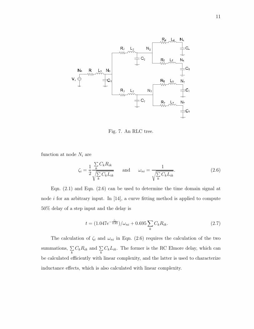
11
! " # ! " # ! " #
" " ! ! ! " # # # ! " #
Fig. 7. An RLC tree.
function at node Ni are
ζi =1
2
∑
k
CkRik
√
∑
kCkLik
and ωni =1
√
∑
kCkLik
. (2.6)
Eqn. (2.1) and Eqn. (2.6) can be used to determine the time domain signal at
node i for an arbitrary input. In [14], a curve fitting method is applied to compute
50% delay of a step input and the delay is
t = (1.047e−ζi
0.85 )/ωni + 0.695∑
k
CkRik. (2.7)
The calculation of ζi and ωni in Eqn. (2.6) requires the calculation of the two
summations,∑
k
CkRik and∑
k
CkLik. The former is the RC Elmore delay, which can
be calculated efficiently with linear complexity, and the latter is used to characterize
inductance effects, which is also calculated with linear complexity.
12
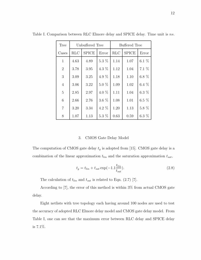
Table I. Comparison between RLC Elmore delay and SPICE delay. Time unit is ns.
Tree Unbuffered Tree Buffered Tree
Cases RLC SPICE Error RLC SPICE Error
1 4.63 4.89 5.3 % 1.14 1.07 6.1 %
2 3.78 3.95 4.3 % 1.12 1.04 7.1 %
3 3.09 3.25 4.9 % 1.18 1.10 6.8 %
4 3.06 3.22 5.0 % 1.09 1.02 6.4 %
5 2.85 2.97 4.0 % 1.11 1.04 6.3 %
6 2.66 2.76 3.6 % 1.08 1.01 6.5 %
7 3.20 3.34 4.2 % 1.20 1.13 5.8 %
8 1.07 1.13 5.3 % 0.63 0.59 6.3 %
3. CMOS Gate Delay Model
The computation of CMOS gate delay tg is adopted from [15]. CMOS gate delay is a
combination of the linear approximation tlin and the saturation approximation tsat,
tg = tlin + tsat exp(−1.1tlintsat
). (2.8)
The calculation of tlin and tsat is related to Eqn. (2.7) [7].
According to [7], the error of this method is within 3% from actual CMOS gate
delay.
Eight netlists with tree topology each having around 100 nodes are used to test
the accuracy of adopted RLC Elmore delay model and CMOS gate delay model. From
Table I, one can see that the maximum error between RLC delay and SPICE delay
is 7.1%.
13
C. RLC Buffering Algorithm
1. Preliminaries
The basic buffering problem includes a routing tree T = (V, E), where V = s0 ∪
Vs ∪ Vn, and E ⊆ V × V . Vertex s0 is the source vertex, Vs is the set of sink vertices
and Vn is the set of internal vertices. Each sink vertex s ∈ Vs is associated with sink
capacitance Cs, and each edge e ∈ E is associated with lumped resistance Re and
capacitance Ce. A buffer library B contains different types of buffers. Each type of
buffer b is associated with an output resistance Rb, input capacitance Cb, intrinsic
delay Kb and a cost Wb. Wb can be measured by area or any other metric, depending
on the optimization objective. Without loss of generality, we assume that the driver at
source s0 is also a buffer. A function f : Vn → 2B specifies the types of buffers allowed
at each internal vertex. A buffer assignment γ is a mapping γ : Vn → B ∪ ∧ where
∧ denotes that no buffer is inserted. The cost of a solution γ is W (γ) =∑
b∈γ Wb.
With the above notations, our RLC buffering problem can be formulated as follows.
RLC Minimum Cost Buffer Insertion Problem: Given a routing tree T =
(V, E), possible buffer positions defined by f , and a buffer library B, find a buffer
assignment γ such that the total cost W (γ) is minimized, the RLC required arrival
time at the driver is no less than a given constant α.
2. Overview of van Ginneken’s Algorithm
To understand the context of the presented algorithms and to define notation, this
section begins with a brief overview of van Ginneken and Lillis’ [1, 5] algorithm. The
algorithm proceeds bottom-up from the leaf nodes toward the driver along a given
routing tree. A set of candidate solutions keeps updated during the process. Each
solution is associated with a three-tuple (C, W, Q), where C denotes the downstream
14
capacitance at the current node, W denotes the cost of the solution and Q refers to
the required arrival time (RAT).
Suppose that a solution γv at position v must “propagate” to an upstream po-
sition u and there is no branching point in between. If no buffer is placed at u,
then only wire delay needs to be considered. Therefore, the new solution γu can be
computed as
C(γu) = C(γv) + Ce,
W (γu) = W (γv),
Q(γu) = Q(γv) − De,
(2.9)
where e = (u, v) and De = Re(Ce
2+ C(γv)). Otherwise, suppose that we add a buffer
bi at u. γu can be then computed as
C(γu) = Cbi,
W (γu) = W (γv) + Wbi,
Q(γu) = Q(γv) − Dbi− De
(2.10)
after buffer insertion. In Eqn. (2.10), Dbirefers to the buffer delay and is computed
as Dbi= R′
bi· C(u) + K ′
bi, where R′
biis the driving resistance of bi but not the slew
resistance of bi, and K ′
biis the intrinsic buffer delay.
An important concept in van Ginneken’s algorithm are non-dominated solutions.
For any two solutions γ1, γ2 at the same node, γ1 dominates γ2 if C(γ1) ≤ C(γ2),
W (γ1) ≤ W (γ2) and Q(γ1) ≥ Q(γ2). Whenever a solution becomes dominated, it is
removed from the solution set. Therefore, only solutions excel in at least one aspect
of downstream capacitance, buffer cost and RAT can survive.
For handling branch merging, suppose that we have obtained all the non-dominated
solutions of left branch Tl and right branch Tr at a branching point vt. The name

15
”left” or ”right” is assigned arbitrarily. Denote the left-branch solution set and the
right-branch solution set by Γl and Γr, respectively. The merging process is per-
formed as follows. For each solution γl ∈ Γl and each solution γr ∈ Γr, generate a
new solution γ′ according to:
C(γ′) = C(γl) + C(γr),
W (γ′) = W (γl) + W (γr),
Q(γ′) = minQ(γl), Q(γr).
(2.11)
At a high level, van Ginneken’s algorithm builds the solution set in a bottom-up
fashion. Assume that we have computed all feasible non-dominated solutions at a
buffer position v. For the immediately upstream buffer position u (without passing
any branching point), we first propagate all solutions up there through performing
wire insertion of (u, v) to each solution. The propagated solutions resemble the choices
when no buffer is inserted at u. Subsequently, for each propagated solution, we
compute a new solution for inserting each buffer. The new solution is inserted into
the solution set as long as it is not dominated by any existing one. The solution set
is meanwhile updated to prune the solutions being dominated by the newcomer. At
a merging point, we carry out the process just described to generate the new solution
set. In this way, we keep climbing up the routing tree until the driver is met. After
pruning solutions violating the timing constraint at driver, we select the best solution
as the one with the smallest cost.
3. Algorithm
Our algorithm shares the same dynamic programming framework as van Ginneken
and Lillis’ algorithm. In our new algorithm, candidate solutions keep being updated
during the procedure from leaf towards the driver, where each solution γ is character-
16
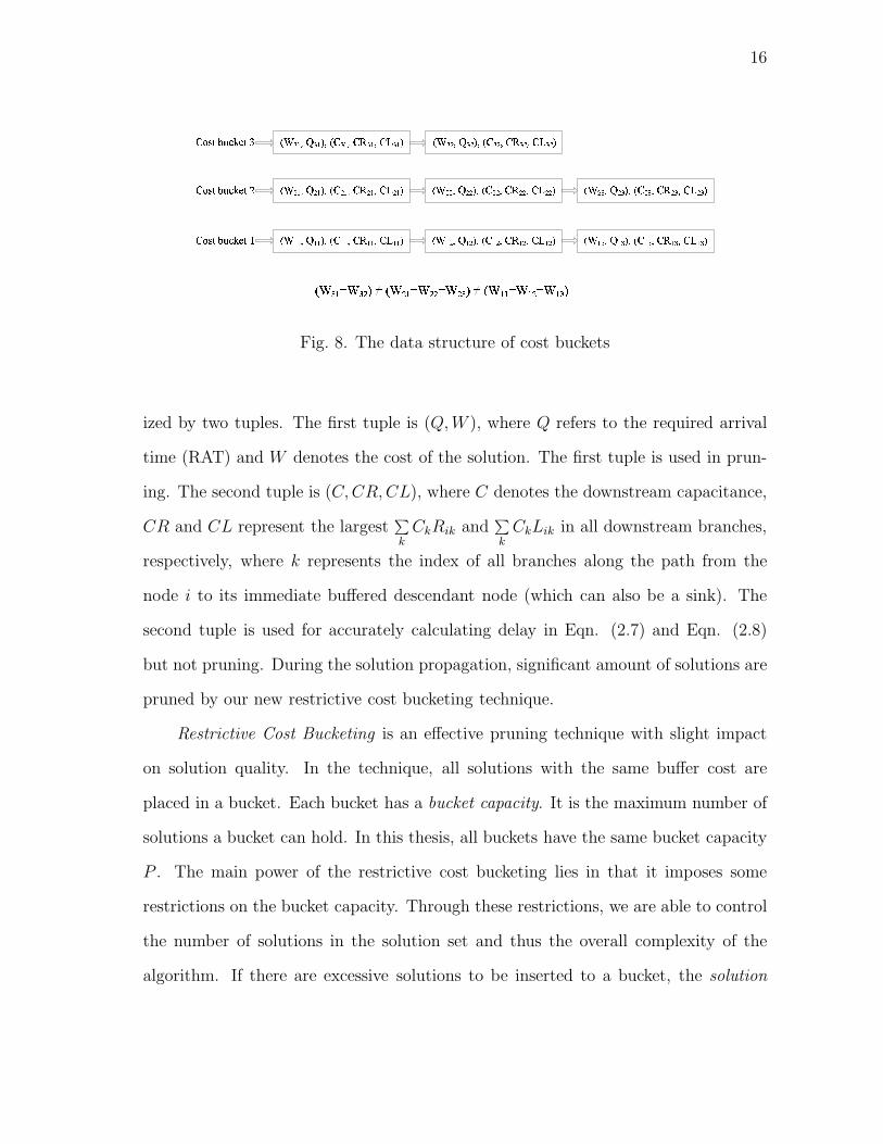
$ % & & ' ( & & ) ' $ * & & ' * + & & ' * , & & ) $ % & - ' ( & - ) ' $ * & - ' * + & - ' * , & - ) $ % & . ' ( & . ) ' $ * & . ' * + & . ' * , & . )$ % - & ' ( - & ) ' $ * - & ' * + - & ' * , - & ) $ % - - ' ( - - ) ' $ * - - ' * + - - ' * , - - ) $ % - . ' ( - . ) ' $ * - . ' * + - . ' * , - . )$ % . & ' ( . & ) ' $ * . & ' * + . & ' * , . & ) $ % . - ' ( . - ) ' $ * . - ' * + . - ' * , . - ) /* 0 1 2 3 4 5 6 7 2 8* 0 1 2 3 4 5 6 7 2 9* 0 1 2 3 4 5 6 7 2 : ; < = > ? < = @ A ? ; < @ > ? < @ @ ? < @ = A ? ; < > > ? < > @ ? < > = AFig. 8. The data structure of cost buckets
ized by two tuples. The first tuple is (Q, W ), where Q refers to the required arrival
time (RAT) and W denotes the cost of the solution. The first tuple is used in prun-
ing. The second tuple is (C, CR, CL), where C denotes the downstream capacitance,
CR and CL represent the largest∑
kCkRik and
∑
kCkLik in all downstream branches,
respectively, where k represents the index of all branches along the path from the
node i to its immediate buffered descendant node (which can also be a sink). The
second tuple is used for accurately calculating delay in Eqn. (2.7) and Eqn. (2.8)
but not pruning. During the solution propagation, significant amount of solutions are
pruned by our new restrictive cost bucketing technique.
Restrictive Cost Bucketing is an effective pruning technique with slight impact
on solution quality. In the technique, all solutions with the same buffer cost are
placed in a bucket. Each bucket has a bucket capacity. It is the maximum number of
solutions a bucket can hold. In this thesis, all buckets have the same bucket capacity
P . The main power of the restrictive cost bucketing lies in that it imposes some
restrictions on the bucket capacity. Through these restrictions, we are able to control
the number of solutions in the solution set and thus the overall complexity of the
algorithm. If there are excessive solutions to be inserted to a bucket, the solution

17
selection procedure will be carried out. The preference of solutions could be based on
various criteria and in our experiments, large slack solutions are preferred.
Figure 8 shows an example of data structure of cost buckets. Eight solutions
are inserted into different cost bucket according to their costs, and solutions with the
same cost are inserted into the same cost bucket.
The procedure of the new buffering algorithm is as follows.
a. Sink
At a sink node, we create a candidate solution set in which each bucket is associated
with a range of buffer costs. A solution is added to a cost bucket associated to zero
buffer cost which can be computed since that Q is equal to the required arrival time
at that sink and C is equal to the sink capacitance. W = 0 and
CL = 0,
CR = 0.(2.12)
After this operation, the size of zero cost bucket is equal to 1 and the size of
other cost bucket is zero.
b. Wire Insertion
Consider to propagate solutions from a node v to its parent node u through edge
e = (u, v). A solution γv at v becomes solution γu at u, C(γu) = C(γv) + Ce and
W (γu) = W (γv),
CR(γu) = CR(γv) + Re · C(γu),
CL(γu) = CL(γv) + Le · C(γu),(2.13)
where Re and Le are wire resistance and inductance, respectively. Since our delay
model is not additive, Q is not updated in the operation of wire insertion. No new
18
solution is added in the solution set, and the size of each cost bucket does not change.
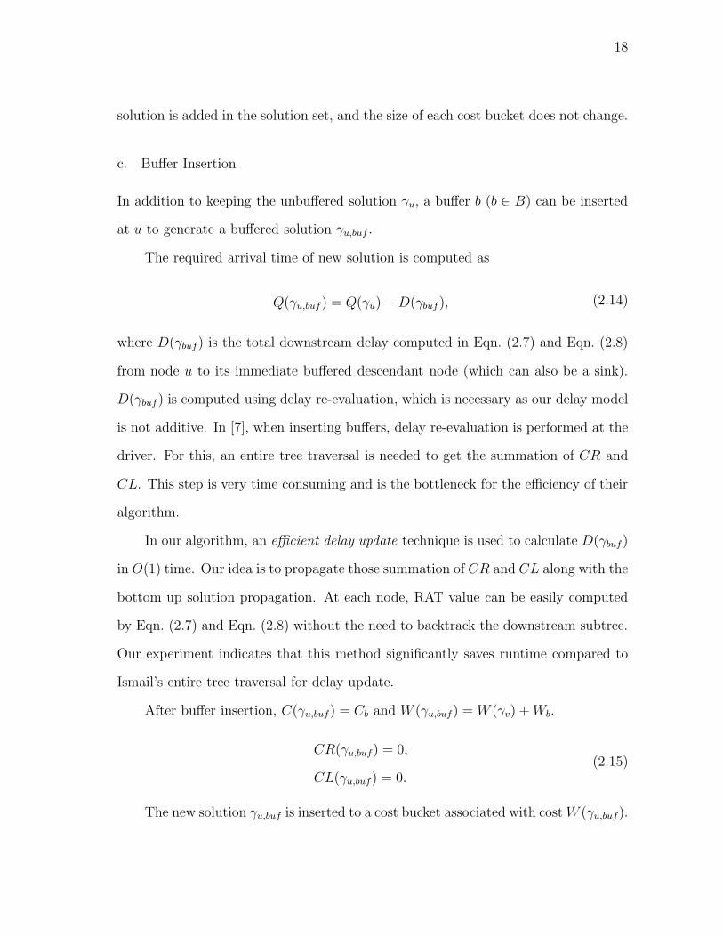
c. Buffer Insertion
In addition to keeping the unbuffered solution γu, a buffer b (b ∈ B) can be inserted
at u to generate a buffered solution γu,buf .
The required arrival time of new solution is computed as
Q(γu,buf) = Q(γu) − D(γbuf), (2.14)
where D(γbuf) is the total downstream delay computed in Eqn. (2.7) and Eqn. (2.8)
from node u to its immediate buffered descendant node (which can also be a sink).
D(γbuf) is computed using delay re-evaluation, which is necessary as our delay model
is not additive. In [7], when inserting buffers, delay re-evaluation is performed at the
driver. For this, an entire tree traversal is needed to get the summation of CR and
CL. This step is very time consuming and is the bottleneck for the efficiency of their
algorithm.
In our algorithm, an efficient delay update technique is used to calculate D(γbuf)
in O(1) time. Our idea is to propagate those summation of CR and CL along with the
bottom up solution propagation. At each node, RAT value can be easily computed
by Eqn. (2.7) and Eqn. (2.8) without the need to backtrack the downstream subtree.
Our experiment indicates that this method significantly saves runtime compared to
Ismail’s entire tree traversal for delay update.
After buffer insertion, C(γu,buf) = Cb and W (γu,buf) = W (γv) + Wb.
CR(γu,buf) = 0,
CL(γu,buf) = 0.(2.15)
The new solution γu,buf is inserted to a cost bucket associated with cost W (γu,buf).
19
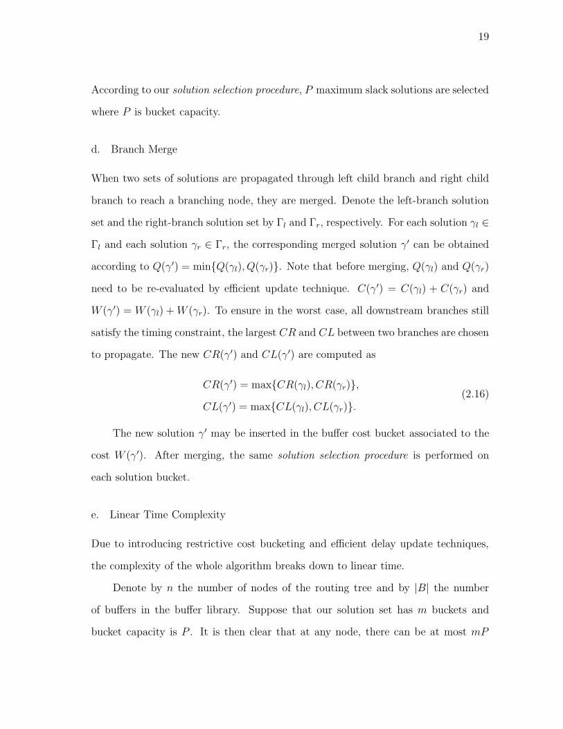
According to our solution selection procedure, P maximum slack solutions are selected
where P is bucket capacity.
d. Branch Merge
When two sets of solutions are propagated through left child branch and right child
branch to reach a branching node, they are merged. Denote the left-branch solution
set and the right-branch solution set by Γl and Γr, respectively. For each solution γl ∈
Γl and each solution γr ∈ Γr, the corresponding merged solution γ′ can be obtained
according to Q(γ′) = minQ(γl), Q(γr). Note that before merging, Q(γl) and Q(γr)
need to be re-evaluated by efficient update technique. C(γ′) = C(γl) + C(γr) and
W (γ′) = W (γl) + W (γr). To ensure in the worst case, all downstream branches still
satisfy the timing constraint, the largest CR and CL between two branches are chosen
to propagate. The new CR(γ′) and CL(γ′) are computed as
CR(γ′) = maxCR(γl), CR(γr),
CL(γ′) = maxCL(γl), CL(γr).(2.16)
The new solution γ′ may be inserted in the buffer cost bucket associated to the
cost W (γ′). After merging, the same solution selection procedure is performed on
each solution bucket.
e. Linear Time Complexity
Due to introducing restrictive cost bucketing and efficient delay update techniques,
the complexity of the whole algorithm breaks down to linear time.
Denote by n the number of nodes of the routing tree and by |B| the number
of buffers in the buffer library. Suppose that our solution set has m buckets and
bucket capacity is P . It is then clear that at any node, there can be at most mP

20
0 1 2 3 4 5 6 7 8 90
5
10
15
20
25
30
35
Buffer Positions
Norm
aliz
ed R
unnin
g T
ime
x 1000
Run Time
Fig. 9. Time complexity of new RLC algorithm with respect to the number of buffer
positions.
solutions. Given this fact, we are to analyze the complexity due to wire insertion,
buffer insertion and branch merging operations. For wire insertion, the number of
solutions do not increase. For buffer insertion, at most |B|mP could be generated
(of course, at most mP can be selected). For branch merging, at most m2P 2 can
be generated. Thus, at any time during the solution propagation, we can have at
most max|B|mP, m2P 2 solutions. By building a balanced binary search tree on
each bucket in the solution set, solution pruning by restrictive cost bucketing can be
certainly completed in max|B|mP, m2P 2 ·O(log P ) time and each delay evaluation
only takes O(1) time since we do not need to traverse any subtree. In practice, we
set m, P to small constants. Since there are at most n candidate buffer positions, it
immediately follows that our algorithm runs in O(n|B|) time.
Figure 9 shows the time complexity of our new algorithm with respect to the

21
number of buffer positions. The buffer library size is 12. The number of buffer
positions is from 138 to 8589. In the figure, the vertical axis is normalized to the
running time of the case with 138 buffer positions. We can see our new algorithm
behaves linearly with the number of buffer positions.
D. Experimental Results
Our new algorithms and algorithm in [8] are implemented in C++. Implementation
of Ismail’s RLC algorithm is borrowed from the author’s webpage. All algorithms
are tested on a Pentium IV computer with a 3.2GHz CPU and 1GB memory. Our
test cases are extracted from an industrial ASIC chip, which consists of 1000 nets
with more than 50000 nodes including sinks, branching nodes and buffer positions.
Among them, 682 nets have ≤ 5 sinks and all the remaining nets have ≤ 20 sinks. The
sink capacitances range from 2.5fF to 200fF . The unit resistance is 16.4Ω/mm, the
unit capacitance is 194.2fF/mm and the unit inductance is 1.0nH/mm. The buffer
library consists of 12 buffers. Buffer resistances range from 30Ω to 360Ω and input
capacitances range from 3.3fF to 40.0fF . The time unit for this section is ps if not
specified. SPICE simulation is based on RLC model in all the experiments below.
For convenience, all algorithms in comparison are listed below together with their
abbreviations.
• van Ginneken-Lillis: van Ginneken and Lillis’ min-cost timing buffering based
on the RC Elmore delay [1, 5].
• Ismail: Ismail’s top-down RLC timing buffering algorithm based on RLC El-
more delay [7].
• Impedance: RLC min-cost timing buffering based on impedance delay [8].

22
• NEW: RLC timing buffering without cost minimization based on RLC Elmore
delay. In NEW, the number of bucket m is set as 1.
• NEW+COST: RLC min-cost timing buffering based on RLC Elmore delay. In
NEW+COST, the number of bucket m is set as 7 and P is equal to 15.
1. Comparison between Ismail and NEW
We compare the number of buffer, SPICE delay and CPU time between Ismail and
NEW. The results on total 1000 nets are summarized in Table II. From Table II, we
make the following observations:
• The solutions from NEW always have less SPICE delay and less buffer area
than those returned by Ismail. Especially, NEW (P = 50) can save up to 8.5%
buffer area than Ismail.
• In addition to returning high quality solutions, NEW also is efficient in terms of
runtime. Especially, NEW (P = 30) can provide up to 4× speedup over Ismail.
The reason behind this phenomenon is that our restrictive cost bucketing and
efficient delay updating techniques tremendously reduce complexity.
• As P increases, the solution quality in NEW also increases and so does the
runtime. This property makes NEW greatly suitable for pratical use since a
tradeoff between solution quality and runtime is easily achieved.
2. Comparison between van Ginneken-Lillis, Impedance and NEW+COST
We compare buffer reduction between van Ginneken-Lillis, Impedance and NEW+COST
algorithms since all these three handle cost minimization. The results on total 1000
nets are summarized in Table III. The solution satisfying the minimum delay condi-
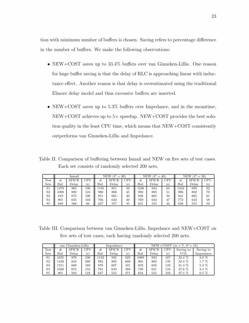
23
tion with minimum number of buffers is chosen. Saving refers to percentage difference
in the number of buffers. We make the following observations:
• NEW+COST saves up to 33.4% buffers over van Ginneken-Lillis. One reason
for huge buffer saving is that the delay of RLC is approaching linear with induc-
tance effect. Another reason is that delay is overestimated using the traditional
Elmore delay model and thus excessive buffers are inserted.
• NEW+COST saves up to 5.3% buffers over Impedance, and in the meantime,
NEW+COST achieves up to 5× speedup. NEW+COST provides the best solu-
tion quality in the least CPU time, which means that NEW+COST consistently
outperforms van Ginneken-Lillis and Impedance.
Table II. Comparison of buffering between Ismail and NEW on five sets of test cases.
Each set consists of randomly selected 200 nets.
Ismail NEW (P = 30) NEW (P = 40) NEW (P = 50)Test # SPICE CPU # SPICE CPU # SPICE CPU # SPICE CPUSets Buf. Delay (s) Buf. Delay (s) Buf. Delay (s) Buf. Delay (s)S1 1270 965 196 1195 951 50 1236 944 64 1242 939 82S2 1008 809 124 980 806 45 992 805 51 986 802 70S3 919 675 106 851 665 40 848 665 50 841 665 61S4 801 645 103 766 643 40 769 644 47 772 643 58S5 640 568 66 627 557 35 631 555 42 628 555 50
Table III. Comparison between van Ginneken-Lillis, Impedance and NEW+COST on
five sets of test cases, each having randomly selected 200 nets.
van Ginneken-Lillis Impedance NEW+COST (m = 7, P = 15)Test # SPICE CPU # SPICE CPU # SPICE CPU Saving to Saving toSets Buf. Delay (s) Buf. Delay (s) Buf. Delay (s) VGL ImpedanceS1 1635 979 330 1132 935 825 1089 933 167 33.4 % 3.8 %S2 1428 843 280 982 802 660 965 802 135 32.4 % 1.7 %S3 1211 688 169 879 667 421 832 658 122 31.3 % 5.3 %S4 1020 672 152 764 643 388 738 641 110 27.6 % 3.4 %S5 861 583 123 627 555 271 624 555 103 27.5 % 0.5 %

24
CHAPTER III
A TWISTED DIFFERENTIAL LINE FOR GLOBAL BUS
Twisted differential line structure can effectively reduce cross-talk noise on global
bus, which foresees a wide applicability. However, measured performance based on
fabricated circuits is much worse than simulated performance based on the layout. It
is suspected that the via resistance variation is the cause.
In this thesis, our extensive simulation confirm this. A new redundant via inser-
tion technique is proposed to reduce via variation and signal distortion. In addition,
a new buffer insertion technique is proposed to synchronize the transmitted signals,
thus further improving the effectiveness of the twisted differential line.
A. Introduction
With the VLSI technology scaling, global buses between function blocks become much
longer and frequencies of signals become much higher. Subsequently, significantly
more crosstalk are observed between neighboring bus lines, which causes the bus
signal transmission unreliable.
Much research effort has been spent on reducing crosstalk and improving signal
integrity on buses. Most of them focus on reducing capacitive crosstalk using single-
end structure, for example, shielding and metal spacing [16]. They are capable of
eliminating capacitive crosstalk since electrical field effect is of short range and tends
to terminate in neighboring metal materials. In contrast, magnetic field effect is of
long range, and thus these techniques can not suppress inductive crosstalk. As signal
frequency increases, inductive crosstalk becomes as important as (i.e., comparable in
magnitude to) capacitative crosstalk and is no longer negligible. Thus, it is imperative
to consider both capacitive and inductive crosstalk in global bus design.
25
Differential signalling is such a technique. It is shown in [17] that 95.7% noise
reduction can be obtained by this technique. However, [17] uses two parallel traces
for each signal line, which can not effectively handle asymmetric noise sources. Thus,
a twisted differential line structure (TDL) is proposed in [18], which differs from
[17] in that the two traces can twist each other (through vias) periodically. This
helps to balance the amount of noise at each trace. It is demonstrated in [19] that
TDL can gain over 90% further noise reduction compared to untwisted differential
structure. This foresees the wide applicability of TDL technique. However, measured
performance based on fabricated circuits is much worse than simulated performance
based on the layout. It is suspected that the via resistance variation is the cause.
The problem aggravates with technology shrinking since both the nominal value and
variation on via resistance are increasing. This imposes a great challenge in making
twisted differential signalling technique practical.
In this thesis, we first analyzed the reason that fabricated TDLs do not perform as
expected. Through extensive simulation, we confirm that the cause of the performance
degradation is via resistance variation. We then propose a new redundant via insertion
technique to reduce the effect of via variation and signal distortion. In addition, we
propose a new buffer insertion technique for signal synchronization.
Experimental results demonstrate a 6GHz signal can be transmitted with high
fidelity using the new approaches. In contrast, only a 100MHz signal can be reli-
ably transmitted using a single-end bus with power/ground shielding. Compared to
conventional twisted differential line structure, our new techniques can reduce the
magnitude of noise by 45% as witnessed in our simulation. Furthermore, compared
to unbuffered twisted differential line structure, the maximum signal phase difference
is reduced from 37ps to 7ps by the new buffer insertion technique.
26
B. Effect of Via Variation
1. Experiments Setup
The following realistic setup applies to all experiments. MOSIS 130nm technology [13]
is used for our simulation. In an 8-bit global bus, each bit occupies an area of
width of 2.5µm, height of 3µm, length of 3200µm, and space between adjacent bits
is 2.5µm. Our aim is to design high speed bus, thus a 6GHz clock signal with a
slew of 10ps is taken as the input signal. The power supply is 1.5V, and we define
the acceptable noise margin is 10% of power supply as in [20], which is 0.15V. If
signal exceeds the acceptable noise margin, we consider that a performance violation
happens. The interconnect is modeled as 50 segments of unit length, and each segment
uses the π model. FastHenry [12] is applied to extract both resistance and inductance.
An accurate empirical model [21] is applied to extract capacitance of interconnects.
SPICE is used for the simulation.
2. Single-end Bus Structure
We perform simulation on the widely used single-end bus structure with power/ground
shielding. The schematic is shown in Figure 10. In this structure, each signal line
is sandwiched by a power trace and a ground trace, which can almost fully protect
the signal line from capacitive crosstalk. Each signal line is also provided with an
adjacent current return path, which could help reduce the inductive crosstalk. To test
the worst-case noise generated on the 8-bit bus, a 6GHz signal is sent to all the inputs
except the one in the middle. The middle line, called observation line, serves as the
observation point for the noise. Buffers are used as drivers and receivers. SPICE
simulation result is shown in Figure 11(a). One sees that the peak noise is 0.35V,
which exceeds the acceptable noise margin.

27
B C D E FG H H I J
K L MG M MG M MK L MG M MK L MG M MK L MG M M
B C D E FB C D E FB C D E FB C D E FB C D E FB C D E FFig. 10. A single-end model of 8-bit global bus. OP denotes the signal observation
point.
0 200 400 600 800 10001
1.1
1.2
1.3
1.4
1.5
1.6
1.7
1.8
1.9
2
Time (ps)
Vo
lta
ge
(vo
lts)
(a)
0 500 1000 1500 20001.2
1.3
1.4
1.5
1.6
1.7
Time (ps)
Voltage (
volts)
Noise of 200MHz signal
Noise of 100MHz signal
Noise of 50MHz signal
(b)
Fig. 11. (a) Noise signal is measured at OP in Figure 10. The peak noise of 6GHz
input signal is 0.35V. (b) The peak noise of 200MHz input signal is 0.18V, of
100MHz is 0.15V and of 50MHz is 0.11V.
28
Since the desired 6GHz signal cannot be transmitted reliably, we investigate
the highest signal frequency which can be achieved using single-end bus. In the
power/ground shielding bus model, the noise will not fall into the acceptable margin
unless we decrease the input signal frequency (signal slew is fixed as 10% of signal
period) to 100MHz. Refer to Figure 11(b). It is clear that the conventional single-
end bus model is not sufficient to handle high frequency signal transmission even if
power/ground shielding technique is incorporated.
3. Standard Twisted Differential Line Structure
In the twisted differential line structure (TDL) in Figure 12, for each bit line, two
parallel traces are used to transmit the complementary signals and the two traces are
twisted periodically. At a twisting point, one trace keeps its route while the other
goes down and then up across metal layers. Two vias are needed for each twisting.
The twisted differential line structure is very effective in noise reduction since each
trace receives balanced noise from the environment, regardless of the location of noise
source.
However, the transmitted signals after fabrication suffer huge distortion even if
the signals function correctly in layout simulation. It is suspected that via resistance
variation is the cause. In order to justify our statement, we perform intensive simula-
tion considering different sources of variation, e.g. gate length, gate oxide thickness,
interconnect height and via resistance.
As a realistic setup, each trace of bus has 4 twisting points, that is, 8 vias in
total for each two complementary traces. The nominal value of the via resistance is
5Ω, and it varies from 3Ω to 7Ω [22]. The nominal value of gate length, gate oxide
thickness and interconnect height is from MOSIS 130nm technology [13]. From our
simulation result in Figure 13(a), one sees that without any variation, the input signal

29
N O PN O QRS T U V
N O WR S T U VRS T U VR S T U VX Y YR S T U VRS T U VR S T U V
N O Z
Fig. 12. A TDL structure of 8-bit global bus with single via.
0 200 400 600 800 1000-0.2
0
0.2
0.4
0.6
0.8
1
1.2
1.4
1.6
1.8
Time (ps)
Vo
lta
ge
(vo
lts)
Input Signal
Output Signal
(a)
0 200 400 600 800 1000-0.2
0
0.2
0.4
0.6
0.8
1
1.2
1.4
1.6
1.8
Time (ps)
Vo
lta
ge
(vo
lts)
Input Signal
Output Signal
(b)
Fig. 13. (a) Signal in TDL structure with single via and without variation. Output sig-
nal is measured at OP4 in Figure 12. (b) Signal in TDL structure with single
via and with via variation. Output signal is measured at OP4 in Figure 12.

30
0 200 400 600 800 10000.5
0.55
0.6
0.65
0.7
0.75
0.8
Time (ps)
Vo
lta
ge
(vo
lts)
Fig. 14. Noise signal in TDL structure with single via. Signal is measured at OP3 in
Figure 12. The peak noise is 0.11V.
can be transmitted in high quality.
A relationship between via resistance variation and other variation is established
in the simulation. With 10% via resistance variation, the impact to the output signal
is equal to 30% gate length variation, 20% gate oxide thickness variation or 15%
interconnect height variation. This demonstrates that the via resistance variation has
a larger impact on the output signal. When worst-case via variation is considered,
the logic failure of output signal happens. From Figure 13(b), one can see that
the input signal originally is 101010101010, however, the output signal turns into
001010101010. These simulations demonstrate that via variation have critical impact
on signal transmission on global bus and via resistance increases with technology
shrinking. As it turns out, the vias are bottlenecks of performance of TDL.
This imposes a great challenge on high-speed bus design. Note that although
signal can not be reliably transmitted when via variation are considered, the noise is
still significantly reduced. The noise is shown in Figure 14. The peak noise is 0.11V,
compared with 0.35V in the single-end structure shown in Figure 11(a).
31
0 1 2 3 4 5 660
65
70
75
80
85
90
95
100
Resistance Difference(Ohm)
Vo
lta
ge
(m
illiv
olts)
(a)
2 3 4 5 6 7 855
60
65
70
Resistance (Ohm)
Vo
lta
ge
(m
illiv
olts)
(b)
Fig. 15. Peak noise is measured at OP3 in Figure 12. (a) The peak noise with respect
to the resistance difference between two neighboring traces. (b) The peak
noise with respect to the resistance in two neighboring traces. The resistance
of two traces is the same.
C. New Twisted Differential Line Structure
Based on a redundant via insertion technique and a buffer insertion technique, a new
twisted differential line structure is proposed. With it, the hurdle of signal distortions
associated with the standard TDL is overcome. This makes the TDL technique, which
is very effective in reducing both capacitive and inductive noise, practical in high speed
global bus design. We envision the new TDL structure to have wide applicability in
practice.
We begin with investigating the relationship between cross-talk noise and redun-
dant via. The effect of redundant via is twofold: First, redundant via reduces the
resistance variation/difference between neighboring traces. Second, redundant via
reduces the nominal resistance value of neighboring traces. Figure 15(a) shows that

32
peak noise increases with the resistance difference between neighboring traces. Fig-
ure 15(b) shows that peak noise decreases with resistance of neighboring traces. The
two figures demonstrate that the twofold effect of redundant via competes each other,
and since the peak noise is more sensitive to the resistance difference, the crosstalk
noise can be reduced by redundant via insertion technique. This observation will be
explored in the following section.
1. Redundant Via Insertion
TDL needs vias to connect between neighboring metal layers. With technology scal-
ing, via size keeps shrinking and via contact resistance keeps increasing. The prob-
lem aggravates since variation on via due to cut misalignment, electro migration and
thermal stress increases. As a consequence, distortions in signal transmission are
observed.
To tackle this issue, we propose to insert redundant vias into the initial design.
Given a via (which is around a twisting point in TDL), putting n−1 additional vias in
its close proximity can reduce the nominal value of the resistance to 1/n and variation
of the conductance to O(1/n2). In addition, doing so will also reduce the effect of
variation on vias. On the other hand, one might wonder the effect of the additional
cost (e.g., power) due to the inserted redundant vias. Since a global bus often has very
few twistings/vias, doubling/tripling them will not cause trouble. In fact, redundant
via methodology has been recommended as an effective technique to improve yield by
major foundries in their 130nm and 90nm processes [23]. Major EDA vendors such
as Cadence and Synopsis have already allowed the feature of redundant via insertion
in bus routing design [24] without violating any design rule. Figure 16 shows two
different layouts using Virtuoso.
As shown in Figure 13(b), standard TDL with single via fails to transmit high
33
1111111111111111111111111111111111111111111111111111111111111111111111
1111111111111111111111111111111111111111111111111111111111111111111111
1111111111111111111111
111111111111111111111111111111111111111111111
11111111111111111111111111111111111111111111111111111111111111111111111111111111111111111111111111111111111111111111111111111111111111111111111111111111111111111111111111111111111111111111111111111111111111111111111111111111111111
111111111111111111111111111111111111111111111111111111111111111111111111111111111111111111111111111111111111111111111111111111111111111111111111111111111111111111111111111111111111111111111111111111111111111111111111111111111111111111111111111111111111111111111111111111
11 111 1
1111
11
11
1111
(a)
1111111111111111111111111111111111111111111111111111111
1111111111111111111111111111111111111111111111111111111
1111111111111111111111
1111111111111111111111111111111111111111111111111111111
111111111111
11111111111111111111
111111111111
1111
111111
1111
11
1111
11111111
1111
(b)
Fig. 16. Two layouts of TDL structure with double vias using Virtuoso. Both designs
are symmetric for delay balance and noise reduction.
34
0 200 400 600 800 1000-0.2
0
0.2
0.4
0.6
0.8
1
1.2
1.4
1.6
1.8
Time (ps)
Vo
lta
ge
(vo
lts)
Input Signal
Output Signal
(a)
0 200 400 600 800 10000.5
0.55
0.6
0.65
0.7
0.75
0.8
Time (ps)
Vo
lta
ge
(vo
lts)
(b)
Fig. 17. (a) Input signal and output signal in TDL with double vias. Output signal
is measured at OP4 in Figure 12. (b) Noise signal in TDL with double vias.
Signal is measured at OP3 in Figure 12. The peak noise is 0.08V.
frequency signal. We apply our redundant via insertion technique in the same simu-
lation environment. Figure 17(a) shows the output signal after adding another via,
which well matches the input signal.
The crosstalk noise is also reduced by redundant via technique. Figure 17(b)
shows the crosstalk noise in TDL with double vias. The peak noise is 0.08V, compared
with 0.11V of standard TDL with single via in Figure 14.
The comparison of TDL performance between single via and double vias is sum-
marized in Table IV. Suc. represents that the noise falls in the acceptable margin
and output signal has no logic failure. When input frequency is higher than 5GHz,
TDL with single via has logic failure in the output. In the contrast, TDL with double
via reliably transmits input signal to the output. In the meantime, the noise and
output delay difference of double via circuit is consistently less than these of single
via circuit.
35
0 200 400 600 800 1000-0.2
0
0.2
0.4
0.6
0.8
1
1.2
1.4
1.6
1.8
Time (ps)
Vo
lta
ge
(vo
lts)
Output Signal 1
Output Signal 2
(a)
0 200 400 600 800 1000-0.2
0
0.2
0.4
0.6
0.8
1
1.2
1.4
1.6
1.8
Time (ps)
Voltage (
volts)
Output Signal 1
Output Signal 2
(b)
Fig. 18. (a) Output signals in twisted differential line structure with double vias. Out-
put signals are measured at OP1 and OP4 in Figure 12. The maximum output
difference is 37ps. (b) The maximum output difference is 7ps.
2. Buffer Insertion
The output signals can be out of synchronization in global bus due to via resistance
difference and delay difference on each trace, which is often observed in our simulation.
An example is shown in Figure 18(a), where the delay difference between the two
output signals is 37ps, which is almost 1/4 of signal period. There are previous works
on applying buffer insertion to global bus design [25]. However, all of them focus only
on noise reduction, since in previous bus design, signal traces are either singled-ended
or not twisted. In the new TDL design, buffer insertion is applied to handle signal
synchronization.
Denote by sync-error the maximum delay difference between signal traces at the
receiver. Thus, we are to reduce sync-error in a bus design by buffer insertion. A
highly effective pruning technique and a buffering pattern based timing evaluation
method are proposed in the algorithm.

36
Table IV. Comparison of TDL performance between single via and double vias.
Test Single Via Double Vias
Freq. Noise Maximum Delay Suc. Noise Maximum Delay Suc.
(volt) Difference(ps) (volt) Difference(ps)
100MHz 0.02 29 YES 0.02 21 YES
500MHz 0.03 42 YES 0.02 21 YES
1GHz 0.04 42 YES 0.03 24 YES
2GHz 0.05 43 YES 0.03 34 YES
3GHz 0.06 44 YES 0.04 34 YES
4GHz 0.06 45 YES 0.05 35 YES
5GHz 0.09 - NO 0.06 35 YES
6GHz 0.11 - NO 0.08 37 YES
The simulation result after buffer insertion is shown in Figure 18(b). The sync-
error decreases to 7ps compared with 37ps in Figure 18(a). As a comparison, we
perform some buffer insertions by hand and the results are consistently worse com-
pared to the above result. The sync-error of our best result by hand is 12ps. Along
with sync-error, crosstalk noise can be further reduced by buffer insertion. The peak
noise is 0.06V, which is 45% of 0.11V in standard TDL with single via.
37
CHAPTER IV
CIRCUIT-WISE BUFFER INSERTION AND GATE SIZING ALGORITHM
WITH SCALABILITY
Most existing buffer insertion algorithms, such as van Ginneken’s algorithm, consider
individual nets and therefore often result in high buffer cost due to over-buffering.
Thus, circuit-wise buffering is necessary to reduce buffer cost. Recently, some circuit-
wise buffering algorithms are proposed, [26, 27, 28, 29]. However, these algorithms are
based on heuristics which are not scalable in handling large circuits. This motivates
us to design a scalable circuit-wise buffer insertion algorithm to handle circuits with
million plus gates.
In this thesis, we present an algorithm two novel features. (1) A circuit partition
technique based on the criticality of the primary inputs. The downstream cones of the
critical primary inputs are solved separately in the linear programming solver. The
circuit partition technique provides high scalability for the algorithm. (2) A linear
programming formulation of non-linear delay versus cost tradeoff. Due to the similar
nature of buffer insertion and gate sizing, gate sizing can also be handled in such a
formulation.
A. Introduction
As VLSI technology enters the nanoscale regime, a great amount of efforts have been
made to reduce interconnect delay. Among them, buffer insertion stands out as an
effective technique for timing optimization. A dramatic rise in on-chip buffer density
has been witnessed [3, 4]. For example, in two recent IBM ASIC designs, 25% gates
are buffers [4].
The most classic work in buffer insertion is van Ginneken’s dynamic programming
38
algorithm [1], which takes an individual net as input and returns the maximum slack
solution in quadratic time. As an extension, buffer cost and buffer library is handled
in [5]. Recently, the time complexity of van Ginnenken’s algorithm is reduced to
O(nlogn) by [30] while keeping its optimality. However, since these works consider
individual nets and lack a global view of the entire circuit, usually the algorithms
result in excessive buffer cost.
The first circuit-wise buffer insertion algorithm [26] is based on Lagrangian re-
laxation, which takes an entire circuit as input instead of an individual net. A critical
path based buffer insertion algorithm is presented in [27]. The timing constrained
buffer minimization problem is formulated as a network flow problem in [28]. A look-
ahead and back-off heuristic is proposed in [29]. However, from their experimental
results, none of these techniques is scalable to handle large circuits. Due to technology
shrinking, millions of gates are placed on a chip, and algorithms without scalability
can not fit into current and future physical synthesis flow. This motivates us to design
a circuit-wise buffering algorithm with scalability to handle million plus gates.
Along with buffer insertion, gate sizing is another important technique for timing
optimization. It is extensively studied, such as [31], [32] and [33]. A posynominal
programming approach is proposed in [31], an exact solution based on convex op-
timization is provided in [32], and a technique based on Lagrangian relaxation is
utilized in [33]. Both gate sizing and buffer insertion attempt to adjust the upstream
capacitance and downstream resistance of a gate/buffer to minimize total delay and
they both provide a tradeoff between delay and cost. Thus, it is beneficial to si-
multaneously handle both in one algorithm. Such an algorithm is proposed in this
thesis.
In this thesis, we propose a novel circuit-wise simultaneous buffer insertion and
gate sizing algorithm. The novel features of the algorithm are summarized as follows.

39
• Circuit partition technique based on the criticality of the primary inputs. The
downstream cones of the critical primary inputs are solved separately in the lin-
ear programming solver. The circuit partition technique provides the scalability
for the algorithm.
• Linear programming formulation of non-linear delay versus cost tradeoff. Based
on the observation that non-linear tradeoff is usually convex, it can be mod-
eled into several linear functions, which can be efficiently solved under linear
programming formulation.
B. Problem Formulation
Without loss of generality, we only focus on the combinational circuit. A placed
and routed combinational circuit is formulated as a directed acyclic graph (DAG)
G = (V, E). An example is shown in Figure 19(a) and Figure 19(b). The set of
nodes V = Vt ∪ Vn, where Vt are primary input (PI), primary output (PO), gate
input and gate output nodes in the circuit, and Vn are internal nodes and candidate
buffer locations on the interconnect. The set of edges E consists of the edges on the
interconnect and internal paths within a gate.
A buffer library B is provided as a part of the problem statement. The buffer
library B contains different types of buffers. Each type of buffer b is associated with
output resistance Rb, input capacitance Cb, intrinsic delay Kb and buffer cost Wb.
Buffer cost Wb can be measured by area, power consumption or any other metric,
depending on the optimization objective.
Each gate is modeled in a similar manner as a buffer. Each gate input node v is
associated with input capacitance Cv and each gate output node u is associated with
output resistance Ru. If xi is the size of the gate, Cj = Cjxi + fj and Ri = Ri/xi,
40
where Cj, Ri and fj are the unit gate area capacitance, unit output resistance and
gate perimeter capacitance. In this thesis, the size of each gate xi is selected from
the gate library S = x1, · · · , xn, and we do not assume to have a huge buffer and
gate library.
Each interconnect edge e is modeled as a π type RC model and is associated
with resistance R(e) and capacitance C(e). Elmore delay is adopted in our work.
The problem of circuit-wise simultaneous buffer insertion and gate sizing
is defined as follows. Given a DAG which represents a placed and routed combina-
tional circuit, possible candidate buffer locations, a buffer library and a gate library,
find a buffering and gate sizing solution such that the total costs of buffers and gates
are minimized, and the required arrival time at each primary input is less than a
given constant constraint.
Routing trees are generated by partitioning the combinational circuit and ignor-
ing all the steiner nodes. An example is shown in Figure 19(c). In each routing tree,
the root is either a PI vertex or a gate output node, while each sink is either a PO
vertex or a gate input node. Each routing tree is identified by its root, which means
that each tree has a corresponding root. For instance, the routing tree with root e,
sink o, h and j can be represented as RT (e). In this routing tree, root e is a gate
output node, sink o is a PO vertex, and sink h and j are gate input nodes.
C. Algorithm
In this section, a novel circuit-wise simultaneous buffer insertion and gate sizing
algorithm is proposed. We first describe the overall flow and then present the key
features of the algorithm: (1) Post-buffering timing estimation technique; (2) Circuit
partition technique; (3) Linear formulation of non-linear delay versus cost tradeoff;

41
[ \ [ ][ ^(a)_
`abc de fg hij kl
mno(b)p
qrst u v wxy z
|~(c)
Fig. 19. (a) A combinational circuit. (b) The corresponding DAG of the circuit. (c)
The corresponding routing trees and gates of the circuit.
42
(4) Linear programming formulation; (5) Considering slew and buffer congestion.
Our algorithm starts with a post-buffering timing estimation [34]. In their es-
timation, they derive a delay equation for an efficient estimation on multi-pin nets.
The required arrival time (RAT) and arrival time (AT) of each node in the circuit
serve as the estimated post-buffering value. A circuit partition technique is proposed
to solve the sub-circuits separately in the linear programming solver. The circuit
partition technique provides the algorithm scalability to handle large circuits, and for
small circuits, the technique is optional since the these circuits can be solved as a
whole within reasonably short time and without partition error.
To generate buffer delay versus cost tradeoff, van Ginneken-Lillis’ dynamic pro-
gramming algorithm is applied to each routing tree. Gate delay versus cost tradeoff
can be created in a similar manner. Based on the observation that non-linear trade-
off is usually convex, delay cost tradeoff curve is modeled into linear programming
format. Moreover, following the approach in [31], the timing constraint buffer/gate
cost minimization problem is formulated into a linear programming problem.
1. Post-buffering Timing Estimation
The circuit-wise algorithm requires an accurate timing analysis for allocating buffer
and gate resources. The conventional static timing analysis is ineffective since de-
lays along circuit paths change dramatically during the procedure of buffer insertion.
Thus, a more accurate timing analysis method is necessary for the circuit-wise buffer
insertion and gate sizing.
A post-buffering timing estimation technique is proposed in [34], which derives
delay equations along a buffered wire segment and applies the equations for the delay
estimation upon multi-pin nets. This approach is adopted in this thesis. In our ex-
periment, we use a medium-size buffer in the library for the estimation. Experimental

43
Fig. 20. The circuit is partitioned into three sub-circuits based on the downstream
cones of primary inputs. The input a is the most critical primary input in the
circuit.
results show that the delay estimation is only 5% off the value of van Ginneken-Lillis’s
algorithm using full buffer library. After the estimation, the AT and RAT of each
node is known, which determines the criticality of each node and helps to allocate
the buffer and gate resources in the following part of the algorithm.
2. Circuit Partition Technique
Due to the near quadratic relationship between the CPU time of the linear program-
ming and the number of gates in the circuit, the linear programming method becomes
prohibitive as the number of gates approaches millions. It is necessary to adopt the
divide-and-conquer scheme to speed up the algorithm. Such a technique is proposed
in the following.
The key components of the circuit partition technique are how to decide the
partition boundary and how to handle side inputs/outputs in the sub-circuits.
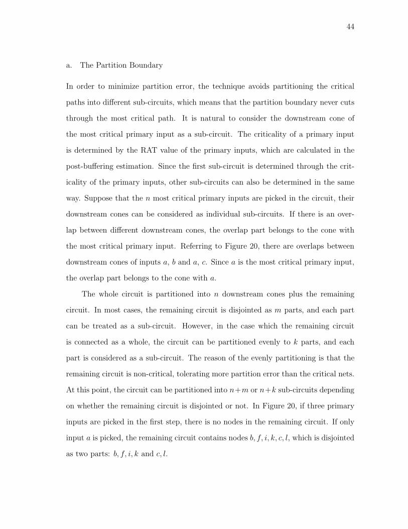
44
a. The Partition Boundary
In order to minimize partition error, the technique avoids partitioning the critical
paths into different sub-circuits, which means that the partition boundary never cuts
through the most critical path. It is natural to consider the downstream cone of
the most critical primary input as a sub-circuit. The criticality of a primary input
is determined by the RAT value of the primary inputs, which are calculated in the
post-buffering estimation. Since the first sub-circuit is determined through the crit-
icality of the primary inputs, other sub-circuits can also be determined in the same
way. Suppose that the n most critical primary inputs are picked in the circuit, their
downstream cones can be considered as individual sub-circuits. If there is an over-
lap between different downstream cones, the overlap part belongs to the cone with
the most critical primary input. Referring to Figure 20, there are overlaps between
downstream cones of inputs a, b and a, c. Since a is the most critical primary input,
the overlap part belongs to the cone with a.
The whole circuit is partitioned into n downstream cones plus the remaining
circuit. In most cases, the remaining circuit is disjointed as m parts, and each part
can be treated as a sub-circuit. However, in the case which the remaining circuit
is connected as a whole, the circuit can be partitioned evenly to k parts, and each
part is considered as a sub-circuit. The reason of the evenly partitioning is that the
remaining circuit is non-critical, tolerating more partition error than the critical nets.
At this point, the circuit can be partitioned into n+m or n+k sub-circuits depending
on whether the remaining circuit is disjointed or not. In Figure 20, if three primary
inputs are picked in the first step, there is no nodes in the remaining circuit. If only
input a is picked, the remaining circuit contains nodes b, f, i, k, c, l, which is disjointed
as two parts: b, f, i, k and c, l.
45
b. Side Inputs and Outputs
After the post-buffering estimation, the RAT and AT of each node are known. The
RAT of boundary nodes are considered as the timing requirement of the side outputs,
and the AT of boundary nodes are considered as the initial delay of the side inputs.
These values are used in the following linear programming inequations.
3. Linear Formulation of Delay vs. Cost Tradeoff
After post-buffering timing estimation, the AT and RAT of each node are known.
Then, van Ginneken-Lillis’ algorithm is carried out for each routing tree in the cir-
cuit. In multiple-sink tree, each sink have its own RAT value and root-to-sink path.
Thus, it has its own buffer delay cost tradeoff curve. To facilitate the curve gener-
ation, we need to augment the data structure of conventional van Ginneken-Lillis’
algorithm, which only maintains the RAT of the most critical sink. In the augmented
data structure, each candidate solution contains a tuple with the updated RAT of all
downstream sinks. Later, these RAT value will be used in linear programming formu-
lation. However, the solutions satisfying the RAT requirement of a sink may violate
the RAT requirement of another. Conventionally, decoupling buffers are inserted at
each branch point to avoid this multi-sink tree problem [26], [28], which wastes a
lot of buffers if the optimal number of buffers is far less than the number of branch
points in the tree. Instead, in the new algorithm, we only keeps one unique solution
set, which is to minimize the maximum delay among all sinks. At the root, only one
buffer delay cost tradeoff curve is returned, which contains delay information of each
sink due to the data structure augmentation. Thus, the tradeoff curve of each sink
can be projected by the tradeoff curve at the root.
Figure 21(a) shows the curves of a tree with 2 sinks: two original curves and two
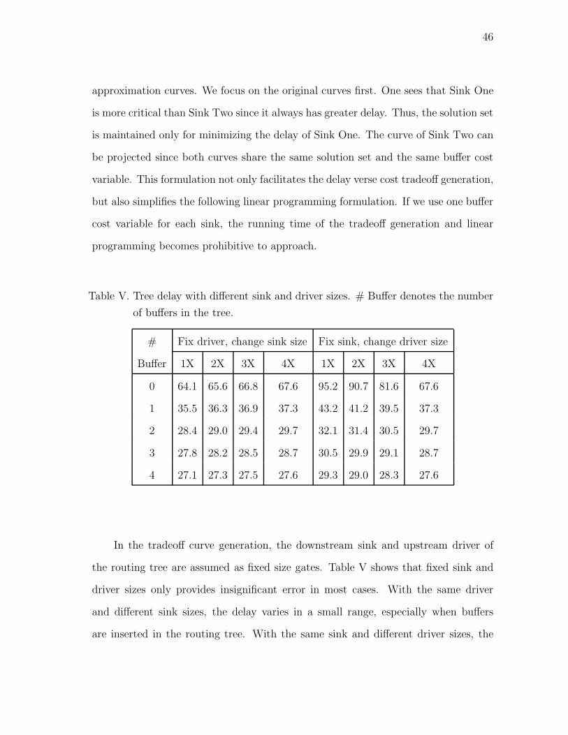
46
approximation curves. We focus on the original curves first. One sees that Sink One
is more critical than Sink Two since it always has greater delay. Thus, the solution set
is maintained only for minimizing the delay of Sink One. The curve of Sink Two can
be projected since both curves share the same solution set and the same buffer cost
variable. This formulation not only facilitates the delay verse cost tradeoff generation,
but also simplifies the following linear programming formulation. If we use one buffer
cost variable for each sink, the running time of the tradeoff generation and linear
programming becomes prohibitive to approach.
Table V. Tree delay with different sink and driver sizes. # Buffer denotes the number
of buffers in the tree.
# Fix driver, change sink size Fix sink, change driver size
Buffer 1X 2X 3X 4X 1X 2X 3X 4X
0 64.1 65.6 66.8 67.6 95.2 90.7 81.6 67.6
1 35.5 36.3 36.9 37.3 43.2 41.2 39.5 37.3
2 28.4 29.0 29.4 29.7 32.1 31.4 30.5 29.7
3 27.8 28.2 28.5 28.7 30.5 29.9 29.1 28.7
4 27.1 27.3 27.5 27.6 29.3 29.0 28.3 27.6
In the tradeoff curve generation, the downstream sink and upstream driver of
the routing tree are assumed as fixed size gates. Table V shows that fixed sink and
driver sizes only provides insignificant error in most cases. With the same driver
and different sink sizes, the delay varies in a small range, especially when buffers
are inserted in the routing tree. With the same sink and different driver sizes, the
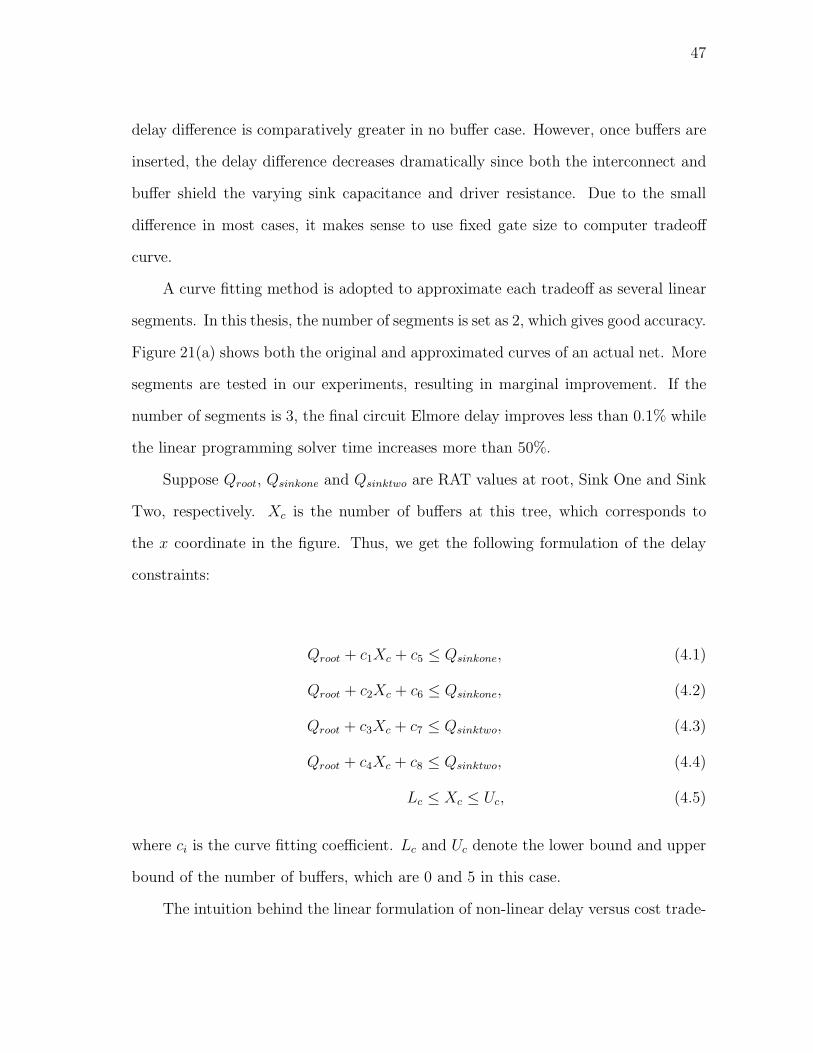
47
delay difference is comparatively greater in no buffer case. However, once buffers are
inserted, the delay difference decreases dramatically since both the interconnect and
buffer shield the varying sink capacitance and driver resistance. Due to the small
difference in most cases, it makes sense to use fixed gate size to computer tradeoff
curve.
A curve fitting method is adopted to approximate each tradeoff as several linear
segments. In this thesis, the number of segments is set as 2, which gives good accuracy.
Figure 21(a) shows both the original and approximated curves of an actual net. More
segments are tested in our experiments, resulting in marginal improvement. If the
number of segments is 3, the final circuit Elmore delay improves less than 0.1% while
the linear programming solver time increases more than 50%.
Suppose Qroot, Qsinkone and Qsinktwo are RAT values at root, Sink One and Sink
Two, respectively. Xc is the number of buffers at this tree, which corresponds to
the x coordinate in the figure. Thus, we get the following formulation of the delay
constraints:
Qroot + c1Xc + c5 ≤ Qsinkone, (4.1)
Qroot + c2Xc + c6 ≤ Qsinkone, (4.2)
Qroot + c3Xc + c7 ≤ Qsinktwo, (4.3)
Qroot + c4Xc + c8 ≤ Qsinktwo, (4.4)
Lc ≤ Xc ≤ Uc, (4.5)
where ci is the curve fitting coefficient. Lc and Uc denote the lower bound and upper
bound of the number of buffers, which are 0 and 5 in this case.
The intuition behind the linear formulation of non-linear delay versus cost trade-
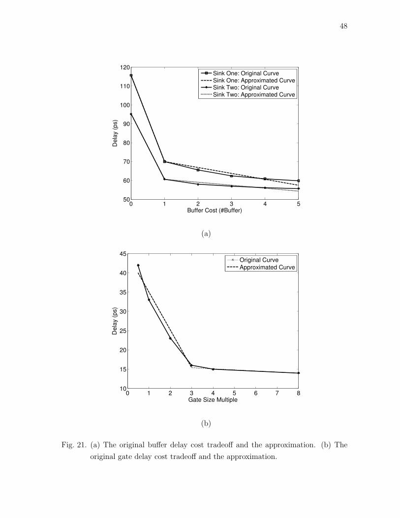
48
0 1 2 3 4 550
60
70
80
90
100
110
120
Buffer Cost (#Buffer)
De
lay (
ps)
Sink One: Original CurveSink One: Approximated CurveSink Two: Original CurveSink Two: Approximated Curve
(a)
0 1 2 3 4 5 6 7 810
15
20
25
30
35
40
45
Gate Size Multiple
De
lay (
ps)
Original Curve
Approximated Curve
(b)
Fig. 21. (a) The original buffer delay cost tradeoff and the approximation. (b) The
original gate delay cost tradeoff and the approximation.

49
a b c Max( , )
Fig. 22. The intuition behind the delay constraint formulation.
off curve is shown in Figure 22. Curve a is a delay cost tradeoff approximation curve
with two segments, which is the max of curve b and curve c. If a variable y is no less
than ya in the range of Lc and Uc, it is equivalent to say that y is no less than yb and
yc in the same range, and vice verse.
One observation is made on the non-linear delay versus cost tradeoff. The op-
timal buffer delay cost tradeoff shows that with buffer cost increasing, the delay
usually decreases and the amount of delay reduction also decreases. In other words,
the approximation curve is convex. Referring to Figure 21(a). The original and
approximated curves are convex.
Gate delay cost tradeoff curves are generated for each type of gate in the gate
library S = x1, · · · , xn in the similar manner. Referring to Figure 21(b). The curve
fitting is applied on gate delay cost tradeoff curves and the convex property can also
be observed.
4. Linear Programming
Linear programming is a well-known technique to handle a large amount of variables,
which is adopted in this algorithm. The formulation follows the approach in [31].

50
The circuit path delay is expressed by the sum of its component delay, which is
interconnect delay or gate delay. In this way, a relationship between the circuit path
delay and its component delay, and the buffer/gate cost is established.
a. LP Formulation
At this point, the circuit-wise simultaneous buffer insertion and gate sizing problem
is formally formulated into a linear programming problem.
Minimizem∑
i=1Xi +
n∑
i=1Xgi
S.t. Qi + ceXi + cf ≤ Qj ,
Li ≤ Xi ≤ Ui, ∀i ∈Primary Input or Gate Output and ∀j ∈Sinks of RT(i),
Qa + cgXgi + ch ≤ Qb,
Lgi ≤ Xgi ≤ Ugi, ∀a ∈Gate Input of gi and ∀b ∈Gate Output of gi,
Qt =User Defined Required Arrival Time, ∀t ∈Primary Output,
Qs ≥ 0, ∀s ∈Primary Input,
where ci is the curve fitting coefficient. Xi is the buffer cost of RT (i) and Xgi is
the gate size of gi. Li, Lgi, Ui and Ugi are their lower bounds and upper bounds,
respectively.
The objective function is the summation of all buffer/gate costs in the circuit.
The timing constraints are interconnect delay and gate delay constraints.
b. Redundant Variables and Constraints Removal
This implementation tip effectively reduces the running time of the linear program-
ming solver. Since the running time increases with the number of variables and
constraints, some “redundant” variables and constraints can be removed to speed
up the solver time. For example, each gate input corresponds to a sink node of its

51
upstream root. Once the RAT of its upstream root or the RAT of the gate output
is known, the RAT of that gate input can be easily calculated. Under this condition,
we can remove all the RAT of gate input by adding the delay of its upstream net and
corresponding gate together. According to the approach in [31], the path delay from
input b to output p in Figure 19(b) can be represented in the following inequations,
Qb + c1Xb + c9 ≤ Qi, (4.6)
Qb + c2Xb + c10 ≤ Qi, (4.7)
Qe + c3Xe + c11 ≤ Qh, (4.8)
Qe + c4Xe + c12 ≤ Qh, (4.9)
Qi + c5Xg2 + c13 ≤ Qm, (4.10)
Qh + c6Xg2 + c14 ≤ Qm, (4.11)
Qm + c7Xm + c15 ≤ Qp, (4.12)
Qm + c8Xm + c16 ≤ Qp. (4.13)
With the tip, the delay formulation is rewrote as follows:
Qb + c1Xb + c9 + c5Xg2 + c13 ≤ Qm, (4.14)
Qb + c2Xb + c10 + c5Xg2 + c13 ≤ Qm, (4.15)
Qe + c3Xe + c11 + c6Xg2 + c14 ≤ Qm, (4.16)
Qe + c4Xe + c12 + c6Xg2 + c14 ≤ Qm, (4.17)
Qm + c7Xm + c15 ≤ Qp, (4.18)
Qm + c8Xm + c16 ≤ Qp, (4.19)
where Qh and Qi are removed from the expression, and the number of constraints
decreases as well. In our implementation, only one tree and one gate are combined,

52
which reduces about 40% linear programming solver time. Further reduction can be
achieved if more trees and gates are combined.
To justify the solutions into practical use, the continuous solution after linear pro-
gramming needs to be mapped to discretized buffer library and gate library. Nearest
rounding is adopted in this thesis. The circuit with discretized solution only provides
insignificant delay overhead compared with the circuit with continuous solution.
5. Considering Slew and Buffer Congestion
As prevailing constraints, both slew constraint and buffer congestion can be incorpo-
rated in the flow.
In van Ginneken-Lillis’ algorithm, slew rate can be included as a forth tuple
along with RAT, total buffer cost and downstream capacitance. Once the solutions
violate the slew constraint, they are pruned. A fast slew buffering algorithm, which
is proposed in our previous work [35], is adopted. It assume a fixed input slew which
allows us to process large volume of nets quickly with small solution degradation.
Refer to [35] for the further details.
In linear programming formulation, congestion constraints can be included. In
congestion region k, let Congestion (k) denote the maximum number of buffers can
be inserted in region k, and n denote the number of trees through that region. The
following constraint for region k can be added in the linear programming formulation.
n∑
i=1Xi∗wire length of Tree i in region k
total wire length of Tree i) ≤
Congestion(k).
The formulation takes probabilistic approach assuming that the buffer location
on each routing tree follows uniform distribution. Thus, the number of buffers in
region k is proportional to the ratio of the wire length in region k and the total wire
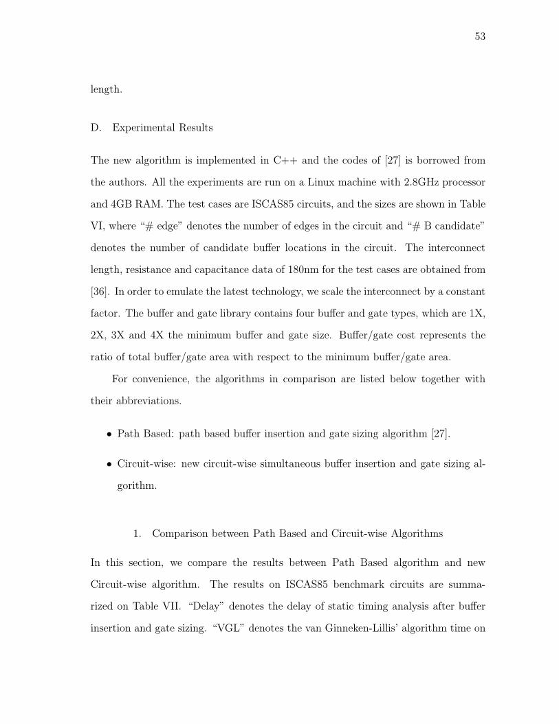
53
length.
D. Experimental Results
The new algorithm is implemented in C++ and the codes of [27] is borrowed from
the authors. All the experiments are run on a Linux machine with 2.8GHz processor
and 4GB RAM. The test cases are ISCAS85 circuits, and the sizes are shown in Table
VI, where “# edge” denotes the number of edges in the circuit and “# B candidate”
denotes the number of candidate buffer locations in the circuit. The interconnect
length, resistance and capacitance data of 180nm for the test cases are obtained from
[36]. In order to emulate the latest technology, we scale the interconnect by a constant
factor. The buffer and gate library contains four buffer and gate types, which are 1X,
2X, 3X and 4X the minimum buffer and gate size. Buffer/gate cost represents the
ratio of total buffer/gate area with respect to the minimum buffer/gate area.
For convenience, the algorithms in comparison are listed below together with
their abbreviations.
• Path Based: path based buffer insertion and gate sizing algorithm [27].
• Circuit-wise: new circuit-wise simultaneous buffer insertion and gate sizing al-
gorithm.
1. Comparison between Path Based and Circuit-wise Algorithms
In this section, we compare the results between Path Based algorithm and new
Circuit-wise algorithm. The results on ISCAS85 benchmark circuits are summa-
rized on Table VII. “Delay” denotes the delay of static timing analysis after buffer
insertion and gate sizing. “VGL” denotes the van Ginneken-Lillis’ algorithm time on
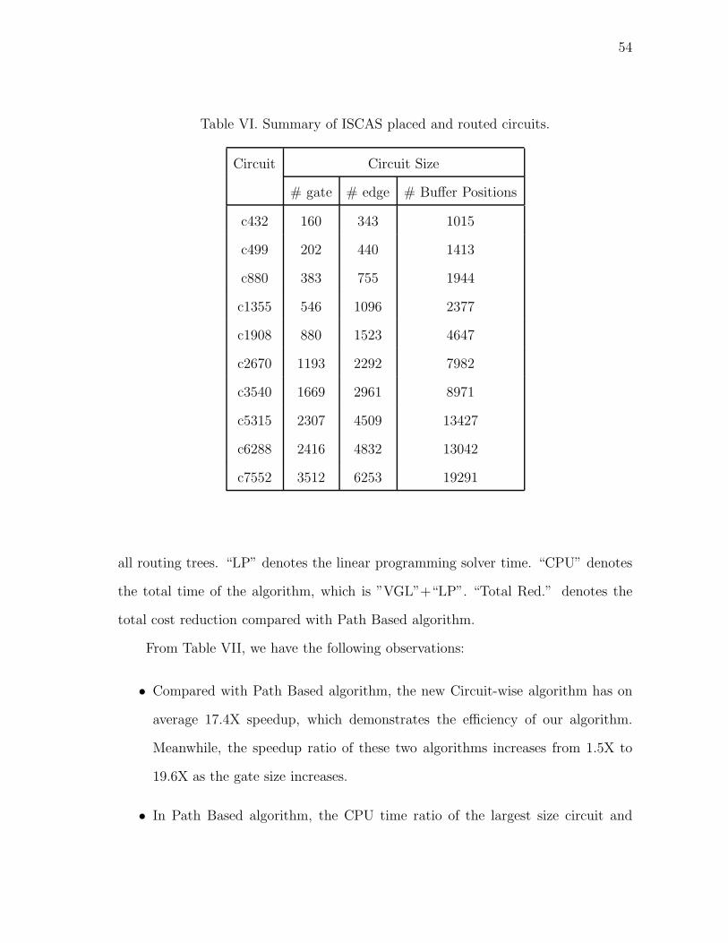
54
Table VI. Summary of ISCAS placed and routed circuits.
Circuit Circuit Size
# gate # edge # Buffer Positions
c432 160 343 1015
c499 202 440 1413
c880 383 755 1944
c1355 546 1096 2377
c1908 880 1523 4647
c2670 1193 2292 7982
c3540 1669 2961 8971
c5315 2307 4509 13427
c6288 2416 4832 13042
c7552 3512 6253 19291
all routing trees. “LP” denotes the linear programming solver time. “CPU” denotes
the total time of the algorithm, which is ”VGL”+“LP”. “Total Red.” denotes the
total cost reduction compared with Path Based algorithm.
From Table VII, we have the following observations:
• Compared with Path Based algorithm, the new Circuit-wise algorithm has on
average 17.4X speedup, which demonstrates the efficiency of our algorithm.
Meanwhile, the speedup ratio of these two algorithms increases from 1.5X to
19.6X as the gate size increases.
• In Path Based algorithm, the CPU time ratio of the largest size circuit and
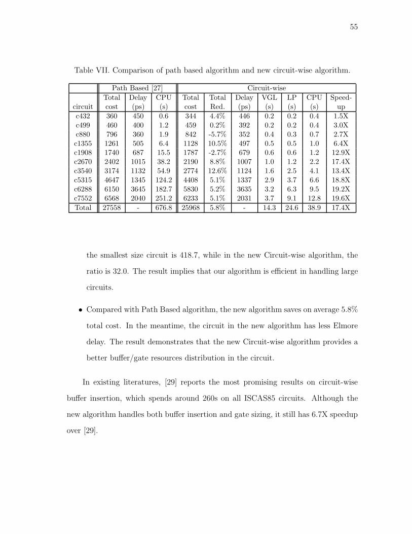
55
Table VII. Comparison of path based algorithm and new circuit-wise algorithm.
Path Based [27] Circuit-wise
Total Delay CPU Total Total Delay VGL LP CPU Speed-circuit cost (ps) (s) cost Red. (ps) (s) (s) (s) up
c432 360 450 0.6 344 4.4% 446 0.2 0.2 0.4 1.5Xc499 460 400 1.2 459 0.2% 392 0.2 0.2 0.4 3.0Xc880 796 360 1.9 842 -5.7% 352 0.4 0.3 0.7 2.7Xc1355 1261 505 6.4 1128 10.5% 497 0.5 0.5 1.0 6.4Xc1908 1740 687 15.5 1787 -2.7% 679 0.6 0.6 1.2 12.9Xc2670 2402 1015 38.2 2190 8.8% 1007 1.0 1.2 2.2 17.4Xc3540 3174 1132 54.9 2774 12.6% 1124 1.6 2.5 4.1 13.4Xc5315 4647 1345 124.2 4408 5.1% 1337 2.9 3.7 6.6 18.8Xc6288 6150 3645 182.7 5830 5.2% 3635 3.2 6.3 9.5 19.2Xc7552 6568 2040 251.2 6233 5.1% 2031 3.7 9.1 12.8 19.6X
Total 27558 - 676.8 25968 5.8% - 14.3 24.6 38.9 17.4X
the smallest size circuit is 418.7, while in the new Circuit-wise algorithm, the
ratio is 32.0. The result implies that our algorithm is efficient in handling large
circuits.
• Compared with Path Based algorithm, the new algorithm saves on average 5.8%
total cost. In the meantime, the circuit in the new algorithm has less Elmore
delay. The result demonstrates that the new Circuit-wise algorithm provides a
better buffer/gate resources distribution in the circuit.
In existing literatures, [29] reports the most promising results on circuit-wise
buffer insertion, which spends around 260s on all ISCAS85 circuits. Although the
new algorithm handles both buffer insertion and gate sizing, it still has 6.7X speedup
over [29].

56
2. The Effect of the Partition Technique
In this section, we compare buffer/gate cost, LP time and circuit Elmore delay be-
tween Circuit-wise without and with the partition technique. In the circuit partition,
the circuit is partitioned into two parts: one is the downstream cone of the most
critical primary input, the other one is the remaining circuit. Note that the VGL
time of Circuit-wise without and with the partition technique are the same since
van Ginneken-Lillis’ algorithm is performed on each routing tree. The results on IS-
CAS85 benchmark circuits are summarized on Table VIII. From Table VIII, we have
the following observations:
• With the circuit partition technique, the LP speedup is on average 37.8%. Due
to the near quadratic relationship between LP time and the number of gates, it
makes sense to achieve the speedup if the divide-and-conquer scheme is applied.
• Circuit-wise with partition uses 0.4% less cost than Circuit-wise without par-
tition. In the meantime, it only has on average 2.3% delay overhead. This
demonstrates that the circuit partition technique effectively speeds up the al-
gorithm with insignificant cost.
The circuit partition technique is optional for circuits with less than ten thousand
gates, since these circuits can be solved as a whole in linear programming solver within
reasonably short time and without any partition error.
3. Testcase with Million Plus Gates
The Circuit-wise algorithm with partition is highly scalable to handle large circuits.
In order to show this, our algorithm is tested on a testcase with million plus gates.
The algorithm selects 150 the most critical primary inputs, and considers their down-
stream cones as sub-circuits. Then, the algorithm partitions the remaining circuit

57
Table VIII. The effect of the partition technique.
Circuit-wise Circuit-wise
without Partition with Partition
Total LP Delay Total LP Delay
circuit Cost (s) (ps) Cost (s) (ps)
c432 344 0.2 446 343 0.2 448
c499 459 0.2 392 444 0.2 404
c880 842 0.4 352 833 0.2 364
c1355 1128 0.5 497 1123 0.3 516
c1908 1787 0.6 679 1778 0.4 688
c2670 2190 1.2 1007 2176 0.5 1040
c3540 2774 2.5 1124 2732 0.8 1182
c5315 4408 3.7 1337 4385 3.1 1363
c6288 5830 6.3 3635 5807 3.6 3722
c7552 6233 9.1 2031 6231 6.0 2034
Total 25968 24.6 - 25852 15.7 -
into another 150 sub-circuits. In our case, the remaining circuit is already disjointed
as 150 parts. The million plus gates testcase is partitioned into 300 sub-circuits in
total.
The VGL time for the million plus gates is 1221 seconds, and the LP time for the
all sub-circuits is 4613 seconds. The total buffer and gate cost is 1872280. From the
results, one sees that the testcase is handled in less than 2 hours, which demonstrates
the scalability of our algorithm.

58
CHAPTER V
CONCLUSION AND FUTURE WORK
A. Conclusion
We present several algorithms in buffer insertion for inductance effects, spacing con-
straints and power management. The first work considers inductance effects to meet
the demand of accurate timing optimization in high frequency digital circuits. Exper-
iments on industrial netlists show that buffer insertion considering inductance effects
can save up to 33.4% of the resources while giving more accurate timing.
The second work proposes redundant via insertion technique to reduce signal
distortions. In addition, a buffer insertion technique is proposed to handle signal
synchronization in TDL design. Our experimental results demonstrate that under a
realistic setup, a 6GHz signal can be transmitted with high fidelity using our new
approaches. In contrast, only a 100MHz signal can be reliably transmitted using a
single-end bus structure.
The third work proposes a scalable buffer insertion and gate sizing algorithm
to handle million plus gates. The core of the new algorithm is to model nonlin-
ear buffer/gate delay cost tradeoff into linear curves. Thus, the timing constraint
buffer/gate cost minimization problem is formulated into a linear programming prob-
lem. Experimental results demonstrate that the new circuit-wise algorithm achieves
on average 17.4X speedup compared with the path based algorithm. With the novel
circuit partition technique, a testcase with million plus gates is handled in less than
2 hours.
59
B. Future Work
The inductance effects on routing can be explored further. Since inductance effects
have significant impact on the delay in global mental layer, in the step of clock
routing, inductance effects need to be considered. For the inductance delay model,
several other delay models like moment matching have not explored yet, which is also
a good direction to study inductance effects on circuit analysis and optimization.
About the circuit-wise buffer insertion and gate sizing, the practical slew con-
straints and buffer congestion constraints can be incorporated into the flow. In van
Ginneken-Lillis’ algorithm, slew rate can be included as a forth tuple along with RAT,
total buffer cost and downstream capacitance. Once the solutions violate the slew
constraint, they are pruned. About buffer congestion, a probabilistic approach as-
suming that the buffer location on each routing tree follows uniform distribution can
be adopted to avoid the congestion problem in the circuit.
60
REFERENCES
[1] L.P.P.P. van Ginneken, “Buffer placement in distributed RC-tree networks for
minimal Elmore delay,” in Proceedings of International Symposium on Circuits
and Systems, Chicago, Illinois, 1990, pp. 865–868.
[2] W.C. Elmore, “The transient response of damped linear networks with particular
regard to wideband amplifiers,” Journal of Applied Physics, vol. 19, no. 1, pp.
55–63, 1948.
[3] P. Saxena and N. Menezes and P. Cocchini and D.A. Kirkpatrick, “Repeater
scaling and its impact on CAD,” IEEE Transactions on Computer-Aided Design,
vol. 23, no. 4, pp. 451–463, 2004.
[4] P.J. Osler, “Placement driven synthesis case studies on two sets of two chips:
hierarchical and flat,” in Proceedings of International Symposium on Physical
Design, San Diego, California, 2004, pp. 190–197.
[5] J. Lillis and C.-K. Cheng and T.-T.Y. Lin, “Optimal wire sizing and buffer
insertion for low power and a generalized delay model,” Journal of Solid State
Circuits, vol. 31, no. 3, pp. 437–447, 1996.
[6] Y.I. Ismail and E.G. Friedman, “Effects of inductance on the propagation delay
and repeater insertion in VLSI circuits,” in Proceedings of the Conference on
Design Automation, New Orleans, Louisiana, 1999, pp. 721–724.
[7] Y.I. Ismail, E.G. Friedman, and J.L. Neves, “Repeater insertion in tree struc-
tured inductive interconnect,” in Proceedings of the International Conference
on Computer-Aided Design, San Jose, California, 2001, pp. 420–424.
61
[8] Z. Jiang, S. Hu, J. Hu, Z. Li, and W. Shi, “A new RLC buffer insertion al-
gorithm,” in Proceedings of the International Conference on Computer-Aided
Design, San Jose, California, 2006, pp. 553–557.
[9] C.J. Alpert, A. Devgan, and S.T. Quay, “Buffer insertion with accurate gate and
interconnect delay computation,” in Proceedings of the Conference on Design
Automation, New Orleans, Louisiana, 1999, pp. 479–484.
[10] K. Gala, V. Zolotov, R. Panda, B. Young, J. Wang, and D. Blaauw, “On-Chip
inductance modeling and analysis,” in Proceedings of the Conference on Design
Automation, Los Angeles, California, 2000, pp. 63–68.
[11] K. Narbos and J. White, “FastCap: A multipole accelerated 3D capacitance
extraction program,” IEEE Transactions on Computer-Aided Design, vol. 10,
no. 11, pp. 1447–1459, 1991.
[12] M. Kamon and M.J. Ttsuk and J.K. White, “FASTHENRY: A multipole accel-
erated 3-D inductance extraction program,” IEEE Transactions on Microwave
Theory and Techniques, vol. 42, no. 9, pp. 1750–1758, 1994.
[13] “Metal oxide semiconductor implementation service,” http://www.mosis.com,
December 2005.
[14] Y.I. Ismail, E.G. Friedman, and J.L. Neves, “Equivalent Elmore delay for RLC
trees,” in Proceedings of the Conference on Design Automation, New Orleans,
Louisiana, 1999, pp. 715–720.
[15] Y.I. Ismail and E.G. Friedman, “Optimal repeater insertion based on a CMOS
delay model for On-Chip RLC interconnect,” in Proceedings of the IEEE ASIC
Conference, Rochester, New York, 1998, pp. 369–373.

62
[16] Y. Massoud, S. Majors, T. Bustami, and J. White, “Layout techniques for min-
imizing on-chip interconnect self inductance,” in Proceedings of the Conference
on Design Automation, San Francico, California, 1998, pp. 566–571.
[17] Y. Massoud, J. Kawa, D. MacMillen, and J. White, “Modeling and analysis of
differential signaling for minimizing inductive cross-talk,” in Proceedings of the
Conference on Design Automation, Las Vegas, Nevada, 2001, pp. 804–809.
[18] S.P. Khatri, A. Mehrotra, R.K. Brayton, A.S. Vincentelli, and R.J.M. Otten, “A
novel vlsi layout fabric for deep sub-micron applications,” in Proceedings of the
Conference on Design Automation, New Orleans, Louisiana, 1999, pp. 491–496.
[19] G. Zhong, K. Roy, and C. Koh, “A twisted-bundle layout structure for minimiz-
ing inductive coupling noise,” in Proceedings of the International Conference on
Computer-Aided Design, San Jose, California, 2000, pp. 406–411.
[20] H.H. Chen and D.D. Ling, “Power supply noise analysis methodology for deep-
submicron vlsi chip design,” in Proceedings of the Conference on Design Au-
tomation, Anaheim, California, 1997, pp. 638–643.
[21] S. Wong, T. Lee, D. Ma, and C. Chao, “An empirical three-dimensional crossover
capacitance model for multilevel interconnect vlsi circuits,” IEEE Transactions
on Semiconductor Manufacturing, vol. 13, no. 2, pp. 219–227, 2000.
[22] G. K. Reeves, A. S. Holland, and P. Leech, “Influence of via liner properties
on the current density and resistance of vias,” in International Conference on
Microelectronics, Nis, Yugoslavia, 2002, pp. 535–538.
[23] G.A. Allan and A.J. Walto, “Automated redundant via placement for increased
yield and reliability,” Sicitation Digital Library, vol. 3216, no. 1, pp. 114–125,
1997.
63
[24] G. Xu, L.-D. Huang, D.Z. Pan, and M.D.F. Wong, “Redundant-via enhanced
maze routing for yield improvement,” in Proceedings of the Conference on Asia
South Pacific Design Automation, Shanghai, China, 2005, pp. 1148–1151.
[25] C.J. Alpert, A. Devgan, and S.T. Quay, “Buffer insertion for noise and delay
optimization,” in Proceedings of the Conference on Design Automation, San
Francico, California, 1998, pp. 362–367.
[26] I.-M. Liu, A. Aziz, D.F. Wong, and H. Zhou, “An efficient buffer insertion
algorithm for large networks based on lagrangian relaxation,” in Proceedings of
International Conference on Computer Design, Austin, Texas, 1999, pp. 210–215.
[27] C.N. Sze and C.J. Alpert and J. Hu and W. Shi, “Path based buffer insertion,”
in Proceedings of the Conference on Design Automation, San Diego, California,
2005, pp. 509–514.
[28] R. Chen and H. Zhou, “Efficient algorithms for buffer insertion in general cir-
cuits based on network flow,” in Proceedings of the International Conference on
Computer-Aided Design, San Jose, California, 2005, pp. 322–326.
[29] M. Waghmode, Z. Li, and W. Shi, “Buffer insertion in large circuits with con-
structive solution search techniques,” in Proceedings of the Conference on Design
Automation, San Francisco, California, 2006, pp. 296–301.
[30] W. Shi and Z. Li, “An O(nlogn) time algorithm for optimal buffer insertion,”
in Proceedings of the Conference on Design Automation, Anaheim, California,
2003, pp. 580–585.
[31] J.P. Fishburn and A.E. Dunlop, “TILOS: A posynomial programming ap-
proach to transistor sizing,” in Proceedings of the International Conference
on Computer-Aided Design, Santa Clara, California, 1985, pp. 326–328.

64
[32] S.S. Sapatnekar, V.B. Rae, P.M. Vaidya, and S.M. Kang, “An exact solution
to the transistor sizing problem for CMOS circuits using convex optimizaiton,”
IEEE Transactions on Computer-Aided Design, vol. 12, no. 11, pp. 1621–1634,
1993.
[33] C.-P. Chin, C.C.N. Chu and D.F. Wong, “Fast and exact simultaneous gate
and wire sizing by lagrangian relaxation,” in Proceedings of the International
Conference on Computer-Aided Design, San Jose, California, 1998, pp. 617–624.
[34] C.J. Alpert, J. Hu, S.S. Sapatnekar and C.N. Sze, “Accurate estimation of global
buffer delay within a floorplan,” in Proceedings of the International Conference
on Computer-Aided Design, San Jose, California, 2004, pp. 706–711.
[35] S. Hu, C.J. Alpert, J. Hu, S. Karandikar, Z. Li, W. Shi, and C.-N. Sze, “Fast
algorithms for slew constrained minimum cost buffering,” in Proceedings of the
Conference on Design Automation, San Francisco, California, 2006, vol. 308-313.
[36] X. Lu and W. Shi, “Layout and parasitic information for iscas circuits,”
http://dropzone.tamu.edu/.xiang/iscas.html, December 2006.
65
VITA
Zhanyuan Jiang received the Bachelor of Science degree from Electrical Engi-
neering department in Shanghai Jiao Tong University, Shanghai, China in 2005. In
August 2005, he started to study towards his Master of Science degree in the Com-
puter Engineering group, Texas A&M University, College Station, TX. His research
interests focus on designing and implementing the algorithms in physical synthesis
flow, especially buffer insertion and gate sizing. His interests also include global bus
design.
The typist for this thesis was Zhanyuan Jiang.