Embed Size (px)
Citation preview
DM
A C
on
trolle
31
Section 31. DMA Controller
r
HIGHLIGHTS
This section of the manual contains the following major topics:
31.1 Introduction.............................................................................................................. 31-2
31.2 Status and Control Registers................................................................................... 31-6
31.3 Modes of Operation ............................................................................................... 31-29
31.4 Channel Control..................................................................................................... 31-40
31.5 Interrupts................................................................................................................ 31-44
31.6 Operation in Power-Saving and Debug Modes ..................................................... 31-46
31.7 Effects of Various Resets....................................................................................... 31-46
31.8 Related Application Notes ..................................................................................... 31-47
31.9 Revision History..................................................................................................... 31-48
© 2007-2013 Microchip Technology Inc. DS60001117H-page 31-1
PIC32 Family Reference Manual
31.1 INTRODUCTION
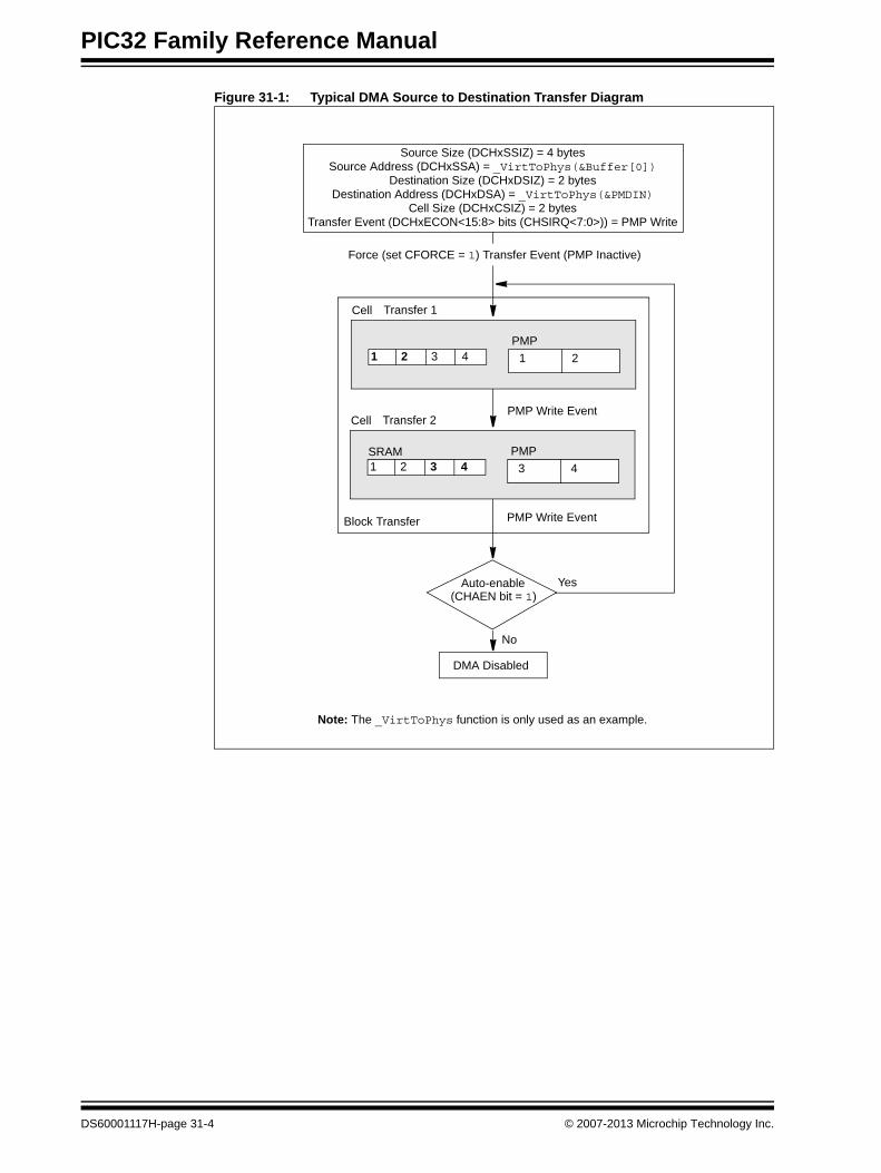
The Direct Memory Access (DMA) controller is a bus master module that is useful for datatransfers between different peripherals without intervention from the CPU. The source anddestination of a DMA transfer can be any of the memory-mapped modules included in the PIC32family of devices. For example, memory, or one of the Peripheral Bus (PB) devices such as theSPI or UART, among others.
Key features of the DMA module include:
• Depending on the device, up to eight identical channels are available, including:
- Auto-Increment Source and Destination Address registers
- Source and Destination Pointers
• Depending on the device, uninterrupted data transfers of up to 64 Kbytes are supported
• Flexible data transfer, featuring the following:
- Transfer granularity down to byte level
- Bytes need not be word-aligned at source and destination
• Fixed priority channel arbitration
• Flexible DMA channel operating modes, including:
- Manual (software) or automatic (interrupt) DMA requests
- One-Shot or Auto-Repeat Block Transfer modes
- Channel-to-channel chaining
• Flexible DMA requests, featuring:
- A DMA request can be selected from any of the peripheral interrupt sources
- Each channel can select any interrupt as its DMA request source
- A DMA transfer abort can be selected from any of the peripheral interrupt sources
- Automatic transfer termination upon a data pattern match
• Multiple DMA channel status interrupts, supplying:
- DMA channel block transfer complete
- Source empty or half-empty
- Destination full or half-full
- DMA transfer aborted due to an external event
- Invalid DMA address generated
• DMA debug support features, including:
- Most recent address accessed by a DMA channel
- Most recent DMA channel to transfer data
• CRC Generation module, featuring:
- CRC module can be assigned to any of the available channels
- Data read from the source can be reordered on some devices
- CRC module is highly configurable
- CRC calculation
Note: This family reference manual section is meant to serve as a complement to devicedata sheets. Depending on the device, this manual section may not apply to allPIC32 devices.
Please consult the note at the beginning of the “Direct Memory Access (DMA)Controller” chapter in the current device data sheet to check whether thisdocument supports the device you are using.
Device data sheets and family reference manual sections are available fordownload from the Microchip Worldwide Web site at: http://www.microchip.com
DS60001117H-page 31-2 © 2007-2013 Microchip Technology Inc.
Section 31. DMA ControllerD
MA
Co
ntro
ller
31
These features are also available in the DMA controller:• Different source and destination sizes
• Memory-to-memory transfers
• Memory-to-peripheral transfers
• Channel auto-enable
• Events start/stop
• Pattern match detection
• Channel chaining
31.1.1 DMA Operation
A DMA channel transfers data from a source to a destination without CPU intervention. Thesource and destination start addresses define the start address of the source and destination,respectively.
Both the source and destination have independently configurable sizes and the number of thetransferred bytes is independent of the source and destination sizes.
A transfer is initiated either by software or by an interrupt request. The user can select anyinterrupt on the device to start a DMA transfer.
Upon transfer initiation, the DMA controller will perform a cell transfer (defined by the cell sizeregister) and the channel remains enabled until all bytes of a block (the larger of source size ordestination size) transfer is complete. When a channel is disabled, further transfers will beprohibited until the channel is re-enabled.
The DMA channel uses separate pointers to keep track of the current word locations at thesource and destination.
Interrupts can be generated when the source/destination pointer is half of the source/destinationsize, or when the source/destination counter reaches the end of the source/destination.
A DMA transfer can be aborted by the software, by a pattern match or by an interrupt event. Thetransfer will also stop when an address error is detected.
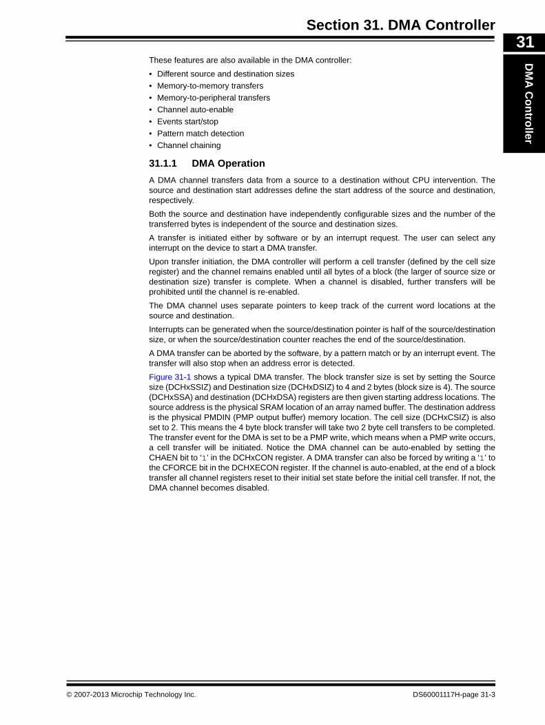
Figure 31-1 shows a typical DMA transfer. The block transfer size is set by setting the Sourcesize (DCHxSSIZ) and Destination size (DCHxDSIZ) to 4 and 2 bytes (block size is 4). The source(DCHxSSA) and destination (DCHxDSA) registers are then given starting address locations. Thesource address is the physical SRAM location of an array named buffer. The destination addressis the physical PMDIN (PMP output buffer) memory location. The cell size (DCHxCSIZ) is alsoset to 2. This means the 4 byte block transfer will take two 2 byte cell transfers to be completed.The transfer event for the DMA is set to be a PMP write, which means when a PMP write occurs,a cell transfer will be initiated. Notice the DMA channel can be auto-enabled by setting theCHAEN bit to ‘1’ in the DCHxCON register. A DMA transfer can also be forced by writing a ‘1’ tothe CFORCE bit in the DCHXECON register. If the channel is auto-enabled, at the end of a blocktransfer all channel registers reset to their initial set state before the initial cell transfer. If not, theDMA channel becomes disabled.
© 2007-2013 Microchip Technology Inc. DS60001117H-page 31-3
PIC32 Family Reference Manual
Figure 31-1: Typical DMA Source to Destination Transfer Diagram
Source Size (DCHxSSIZ) = 4 bytesSource Address (DCHxSSA) = _VirtToPhys(&Buffer[0])
Destination Size (DCHxDSIZ) = 2 bytesDestination Address (DCHxDSA) = _VirtToPhys(&PMDIN)
Cell Size (DCHxCSIZ) = 2 bytesTransfer Event (DCHxECON<15:8> bits (CHSIRQ<7:0>)) = PMP Write
Cell Transfer 1
PMP Write Event
PMP Write Event
Yes
No
DMA Disabled
Block Transfer
PMP1 2 3 4 1 2
Cell Transfer 2
PMPSRAM1 2 3 4 3 4
Auto-enable(CHAEN bit = 1)
Force (set CFORCE = 1) Transfer Event (PMP Inactive)
Note: The _VirtToPhys function is only used as an example.
DS60001117H-page 31-4 © 2007-2013 Microchip Technology Inc.
Section 31. DMA ControllerD
MA
Co
ntro
ller
31
Figure 31-2: DMA Module Block DiagramChannel 0 Control
Channel 1 Control
Channel ‘x’ Control
SEL
SEL
Y
I0
I1
I2
In
INT
PIC32 CPU
IS DS DMA
Global Control(DMACON)
Priority Interrupt Controller
System Bus
Flash Memory Data Ram
Peripheral
Pri
ority
Arb
itra
tion
© 2007-2013 Microchip Technology Inc. DS60001117H-page 31-5
PIC32 Family Reference Manual
31.2 STATUS AND CONTROL REGISTERS
The DMA module consists of the following Special Function Registers (SFRs):
• DMACON: DMA Controller Control Register
This register configures the corresponding DMA channel.
• DMASTAT: DMA Status Register
This register contains the status of the last read or write transfer that occurred.
• DMAADDR: DMA Address Register
This register contains the address of the most recent DMA transfer.
• DCRCCON: DMA CRC Control Register
This register controls the CRC of the DMA and how it will function.
• DCRCDATA: DMA CRC Data Register
This register sets the initial value of the CRC generator. Writing to this register will seed theCRC generator. Reading from this register will return the current value of the CRC.
• DCRCXOR: DMA CRCXOR Enable Register
This register provides a description of the generator polynomial for CRC calculation.
• DCHxCON: DMA Channel ‘x’ Control Register
This register controls the configuration of a specific DMA channel.
• DCHxECON: DMA Channel ‘x’ Event Control Register
This register controls the event for a specific DMA channel.
• DCHxINT: DMA Channel ‘x’ Interrupt Control Register
This register controls the DMA interrupt for a specific DMA channel.
• DCHxSSA: DMA Channel ‘x’ Source Start Address Register
This register configures the source start address for a specific DMA channel.
• DCHxDSA: DMA Channel ‘x’ Destination Start Address Register
This register configures the destination start address for a specific DMA channel.
• DCHxSSIZ: DMA Channel ‘x’ Source Size Register
This register configures the source size for a specific DMA channel.
• DCHxDSIZ: DMA Channel ‘x’ Destination Size Register
This register configures the destination size for a specific DMA channel.
• DCHxSPTR: DMA Channel ‘x’ Source Pointer Register
This register contains the address of the current location of the source for a specific DMAchannel.
• DCHxDPTR: DMA Channel ‘x’ Destination Pointer Register
This register contains the address of the current location of the destination for a specificDMA channel.
• DCHxCSIZ: DMA Channel ‘x’ Cell Size Register
This register configures how many transfers can occur per event for a specific DMA channel.
• DCHxCPTR: DMA Channel ‘x’ Cell Pointer Register
This register counts how many transfers have occurred since the last event for a specificDMA channel.
• DCHxDAT: DMA Channel ‘x’ Pattern Data Register
This register contains data to be matched to allow a terminate on match for a specific DMAchannel.
Note: A PIC32 device may have one or more DMA channels. An ‘x’ used in the names ofControl/Status bits and registers denotes the particular channel. Refer to the“Direct Memory Access Controller” chapter of the specific device data sheet formore details.
DS60001117H-page 31-6 © 2007-2013 Microchip Technology Inc.
© 2007-2013 M
icrochip Technolo
gy Inc.
DS
60001117H
-page 31-7
Sectio
n 31. D
MA
Co
ntro
llerDMA Controller
31
T mmary, that include a detailed description ofe
T
Bit 20/4 Bit 19/3 Bit 118/2 Bit 17/1 Bit 16/0
— — — — —
SUSPEND DMABUSY(2) — — —
— — — — —
— RDWR(2) DMACH<2:0>(2)
— — — — —
— — CRCCH<2:0>(2)
— — — — —
CHAEN — CHEDET CHPRI<1:0>
CHAIRQ<7:0>
SIRQEN AIRQEN — — —
CHDHIE CHBCIE CHCCIE CHTAIE CHERIE
CHDHIF CHBCIF CHCCIF CHTAIF CHERIF
— — — — —
— — — — —
— — — — —
e name with CLR, SET, and INV appended to the end of gister. Reads from these registers should be ignored.
ailability.
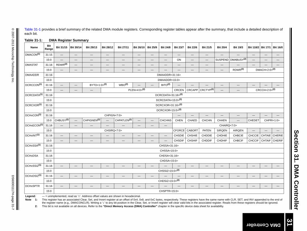
able 31-1 provides a brief summary of the related DMA module registers. Corresponding register tables appear after the suach bit.
able 31-1: DMA Register Summary
NameBit
RangeBit 31/15 Bit 30/14 Bit 29/13 Bit 28/12 Bit 27/11 Bit 26/10 Bit 25/9 Bit 24/8 Bit 23/7 Bit 22/6 Bit 21/5
DMACON(1) 31:15 — — — — — — — — — — —
15:0 — — — — — — — — ON — —
DMASTAT 31:16 RDWR(2) — — — — — — — — — —
15:0 — — — — — — — — — — —
DMAADDR 31:16 DMAADDR<31:16>
15:0 DMAADDR<15:0>
DCRCCON(1) 31:16 — — BYTO<1:0>(2) WBO(2) — — BITO(2) — — —
15:0 — — — PLEN<4:0>(2) CRCEN CRCAPP CRCTYP(2)
DCRCDATA(1) 31:16 DCRCDATA<31:16>(2)
15:0 DCRCDATA<15:0>(2)
DCRCXOR(1) 31:16 DCRCXOR<31:16>(2)
15:0 DCRCXOR<15:0>(2)
DCHxCON(1) 31:16 CHPIGN<7:0> — — —
15:0 CHBUSY(2) — CHPIGNEN(2) — CHPATLEN(2) — — CHCHNS CHEN CHAED CHCHN
DCHxECON(1) 31:16 — — — — — — — —
15:0 CHSIRQ<7:0> CFORCE CABORT PATEN
DCHxINT(1) 31:16 — — — — — — — — CHSDIE CHSHIE CHDDIE
15:0 — — — — — — — — CHSDIF CHSHIF CHDDIF
DCHxSSA(1) 31:16 CHSSA<31:16>
15:0 CHSSA<15:0>
DCHxDSA 31:16 CHDSA<31:16>
15:0 CHDSA<15:0>
DCHxSSIZ(1) 31:16 — — — — — — — — — — —
15:0 CHSSIZ<15:0>(2)
DCHxDSIZ(1) 31:16 — — — — — — — — — — —
15:0 CHDSIZ<15:0>(2)
DCHxSPTR 31:16 — — — — — — — — — — —
15:0 CHSPTR<15:0>
Legend: — = unimplemented, read as ‘0’. Address offset values are shown in hexadecimal.Note 1: This register has an associated Clear, Set, and Invert register at an offset of 0x4, 0x8, and 0xC bytes, respectively. These registers have the sam
the register name (e.g., DMACONCLR). Writing a ‘1’ to any bit position in the Clear, Set, or Invert register will clear valid bits in the associated re2: This bit is not available on all devices. Refer to the “Direct Memory Access (DMA) Controller” chapter in the specific device data sheet for av
PIC
32 Fam
ily Referen
ce Man
ual
DS
60001117H-page 31-8
© 2007-2013 M
icrochip Technolo
gy Inc.
— — — — —
— — — — —
— — — — —
— — — — —
CHPDAT<7:0>
1/5 Bit 20/4 Bit 19/3 Bit 118/2 Bit 17/1 Bit 16/0
e same name with CLR, SET, and INV appended to the end of ted register. Reads from these registers should be ignored.or availability.
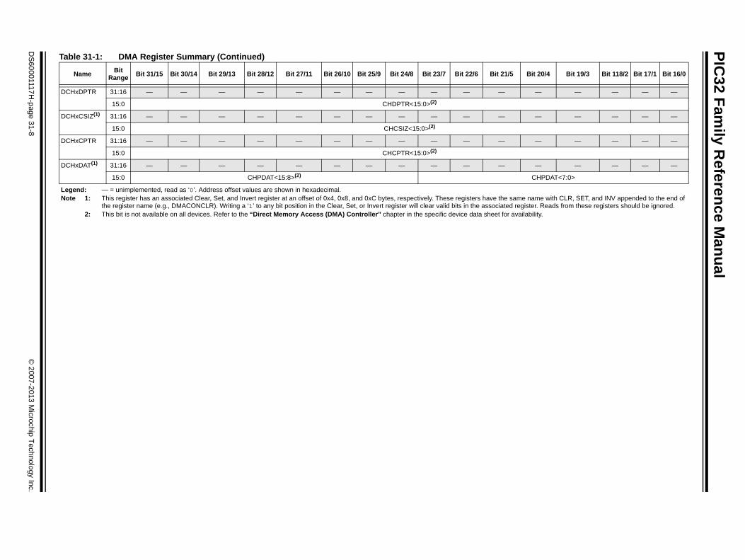
DCHxDPTR 31:16 — — — — — — — — — — —
15:0 CHDPTR<15:0>(2)
DCHxCSIZ(1) 31:16 — — — — — — — — — — —
15:0 CHCSIZ<15:0>(2)
DCHxCPTR 31:16 — — — — — — — — — — —
15:0 CHCPTR<15:0>(2)
DCHxDAT(1) 31:16 — — — — — — — — — — —
15:0 CHPDAT<15:8>(2)
Table 31-1: DMA Register Summary (Continued)
NameBit
RangeBit 31/15 Bit 30/14 Bit 29/13 Bit 28/12 Bit 27/11 Bit 26/10 Bit 25/9 Bit 24/8 Bit 23/7 Bit 22/6 Bit 2
Legend: — = unimplemented, read as ‘0’. Address offset values are shown in hexadecimal.Note 1: This register has an associated Clear, Set, and Invert register at an offset of 0x4, 0x8, and 0xC bytes, respectively. These registers have th
the register name (e.g., DMACONCLR). Writing a ‘1’ to any bit position in the Clear, Set, or Invert register will clear valid bits in the associa2: This bit is not available on all devices. Refer to the “Direct Memory Access (DMA) Controller” chapter in the specific device data sheet f
Section 31. DMA ControllerD
MA
Co
ntro
ller
31
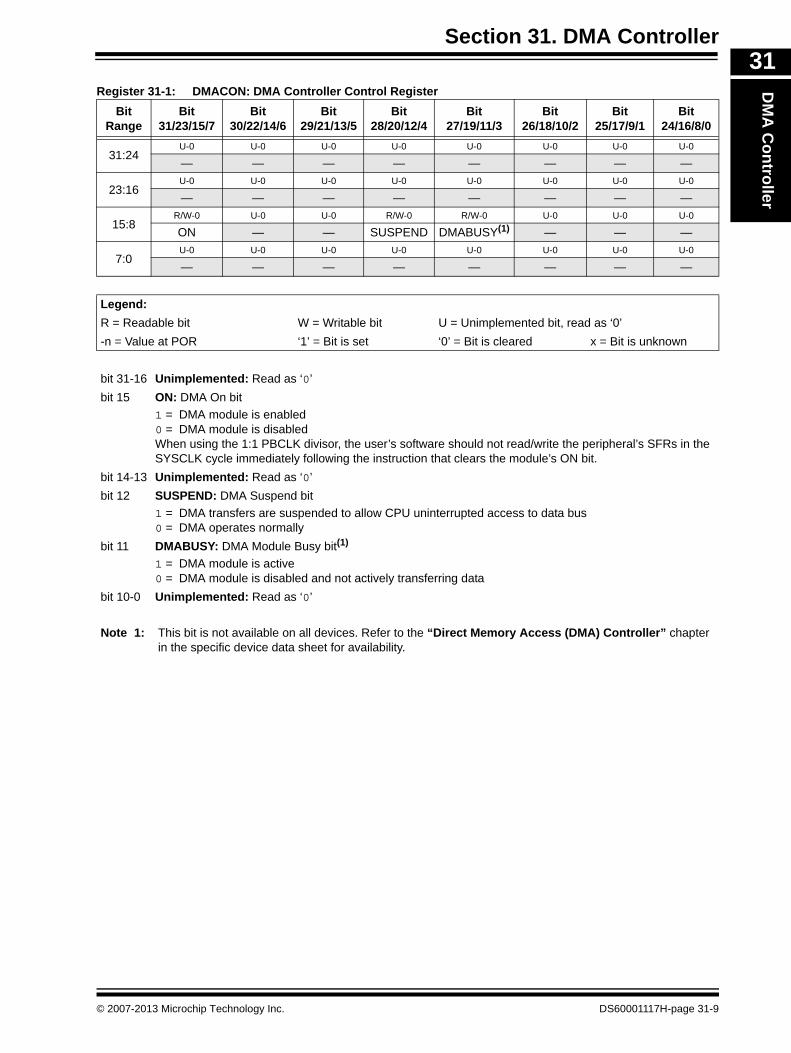
Register 31-1: DMACON: DMA Controller Control RegisterBit Range
Bit31/23/15/7
Bit30/22/14/6
Bit29/21/13/5
Bit28/20/12/4
Bit27/19/11/3
Bit26/18/10/2
Bit25/17/9/1
Bit24/16/8/0
31:24U-0 U-0 U-0 U-0 U-0 U-0 U-0 U-0
— — — — — — — —
23:16U-0 U-0 U-0 U-0 U-0 U-0 U-0 U-0
— — — — — — — —
15:8R/W-0 U-0 U-0 R/W-0 R/W-0 U-0 U-0 U-0
ON — — SUSPEND DMABUSY(1) — — —
7:0U-0 U-0 U-0 U-0 U-0 U-0 U-0 U-0
— — — — — — — —
Legend:
R = Readable bit W = Writable bit U = Unimplemented bit, read as ‘0’
-n = Value at POR ‘1’ = Bit is set ‘0’ = Bit is cleared x = Bit is unknown
bit 31-16 Unimplemented: Read as ‘0’
bit 15 ON: DMA On bit
1 = DMA module is enabled0 = DMA module is disabledWhen using the 1:1 PBCLK divisor, the user’s software should not read/write the peripheral’s SFRs in the SYSCLK cycle immediately following the instruction that clears the module’s ON bit.
bit 14-13 Unimplemented: Read as ‘0’
bit 12 SUSPEND: DMA Suspend bit
1 = DMA transfers are suspended to allow CPU uninterrupted access to data bus0 = DMA operates normally
bit 11 DMABUSY: DMA Module Busy bit(1)
1 = DMA module is active0 = DMA module is disabled and not actively transferring data
bit 10-0 Unimplemented: Read as ‘0’
Note 1: This bit is not available on all devices. Refer to the “Direct Memory Access (DMA) Controller” chapter in the specific device data sheet for availability.
© 2007-2013 Microchip Technology Inc. DS60001117H-page 31-9
PIC32 Family Reference Manual
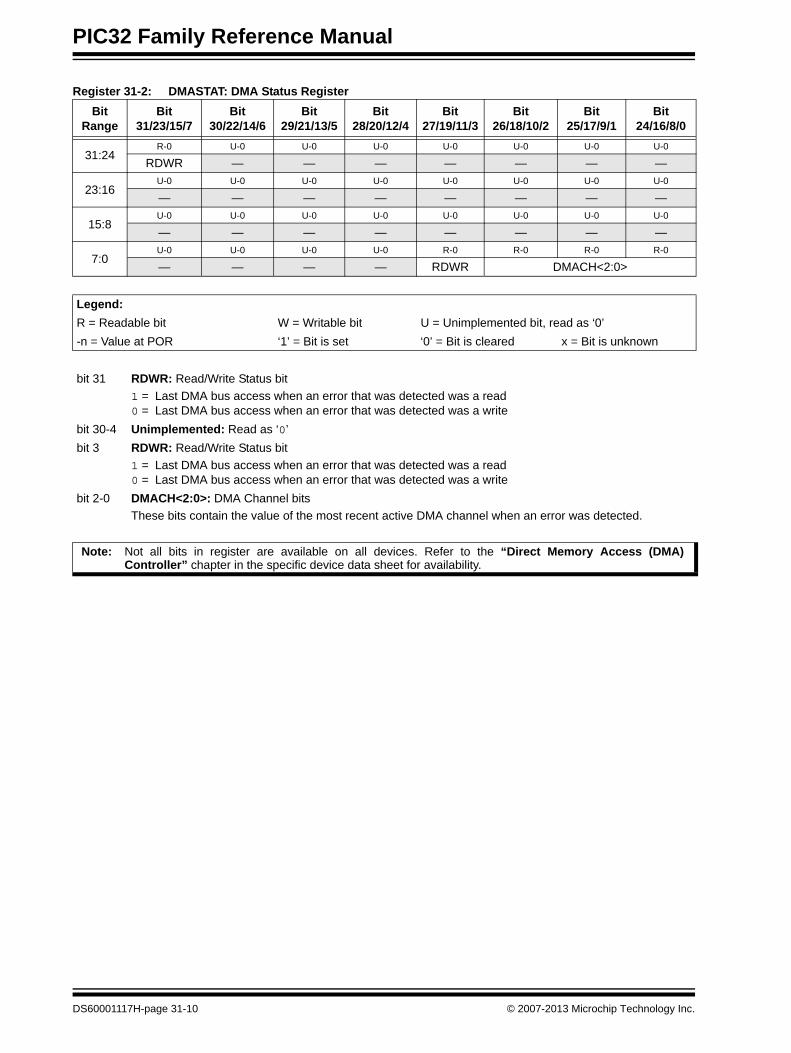
Register 31-2: DMASTAT: DMA Status Register
Bit Range
Bit31/23/15/7
Bit30/22/14/6
Bit29/21/13/5
Bit28/20/12/4
Bit27/19/11/3
Bit26/18/10/2
Bit25/17/9/1
Bit24/16/8/0
31:24R-0 U-0 U-0 U-0 U-0 U-0 U-0 U-0
RDWR — — — — — — —
23:16U-0 U-0 U-0 U-0 U-0 U-0 U-0 U-0
— — — — — — — —
15:8U-0 U-0 U-0 U-0 U-0 U-0 U-0 U-0
— — — — — — — —
7:0U-0 U-0 U-0 U-0 R-0 R-0 R-0 R-0
— — — — RDWR DMACH<2:0>
Legend:
R = Readable bit W = Writable bit U = Unimplemented bit, read as ‘0’
-n = Value at POR ‘1’ = Bit is set ‘0’ = Bit is cleared x = Bit is unknown
bit 31 RDWR: Read/Write Status bit
1 = Last DMA bus access when an error that was detected was a read0 = Last DMA bus access when an error that was detected was a write
bit 30-4 Unimplemented: Read as ‘0’
bit 3 RDWR: Read/Write Status bit
1 = Last DMA bus access when an error that was detected was a read0 = Last DMA bus access when an error that was detected was a write
bit 2-0 DMACH<2:0>: DMA Channel bits
These bits contain the value of the most recent active DMA channel when an error was detected.
Note: Not all bits in register are available on all devices. Refer to the “Direct Memory Access (DMA)Controller” chapter in the specific device data sheet for availability.
DS60001117H-page 31-10 © 2007-2013 Microchip Technology Inc.
Section 31. DMA ControllerD
MA
Co
ntro
ller
31
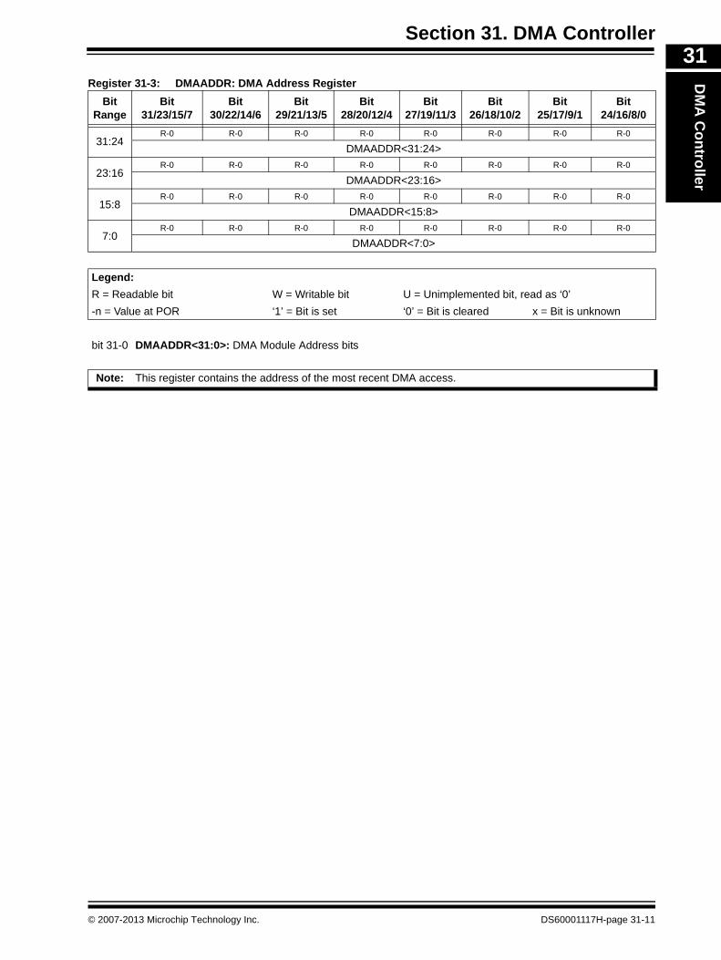
Register 31-3: DMAADDR: DMA Address RegisterBit Range
Bit31/23/15/7
Bit30/22/14/6
Bit29/21/13/5
Bit28/20/12/4
Bit27/19/11/3
Bit26/18/10/2
Bit25/17/9/1
Bit24/16/8/0
31:24R-0 R-0 R-0 R-0 R-0 R-0 R-0 R-0
DMAADDR<31:24>
23:16R-0 R-0 R-0 R-0 R-0 R-0 R-0 R-0
DMAADDR<23:16>
15:8R-0 R-0 R-0 R-0 R-0 R-0 R-0 R-0
DMAADDR<15:8>
7:0R-0 R-0 R-0 R-0 R-0 R-0 R-0 R-0
DMAADDR<7:0>
Legend:
R = Readable bit W = Writable bit U = Unimplemented bit, read as ‘0’
-n = Value at POR ‘1’ = Bit is set ‘0’ = Bit is cleared x = Bit is unknown
bit 31-0 DMAADDR<31:0>: DMA Module Address bits
Note: This register contains the address of the most recent DMA access.
© 2007-2013 Microchip Technology Inc. DS60001117H-page 31-11
PIC32 Family Reference Manual
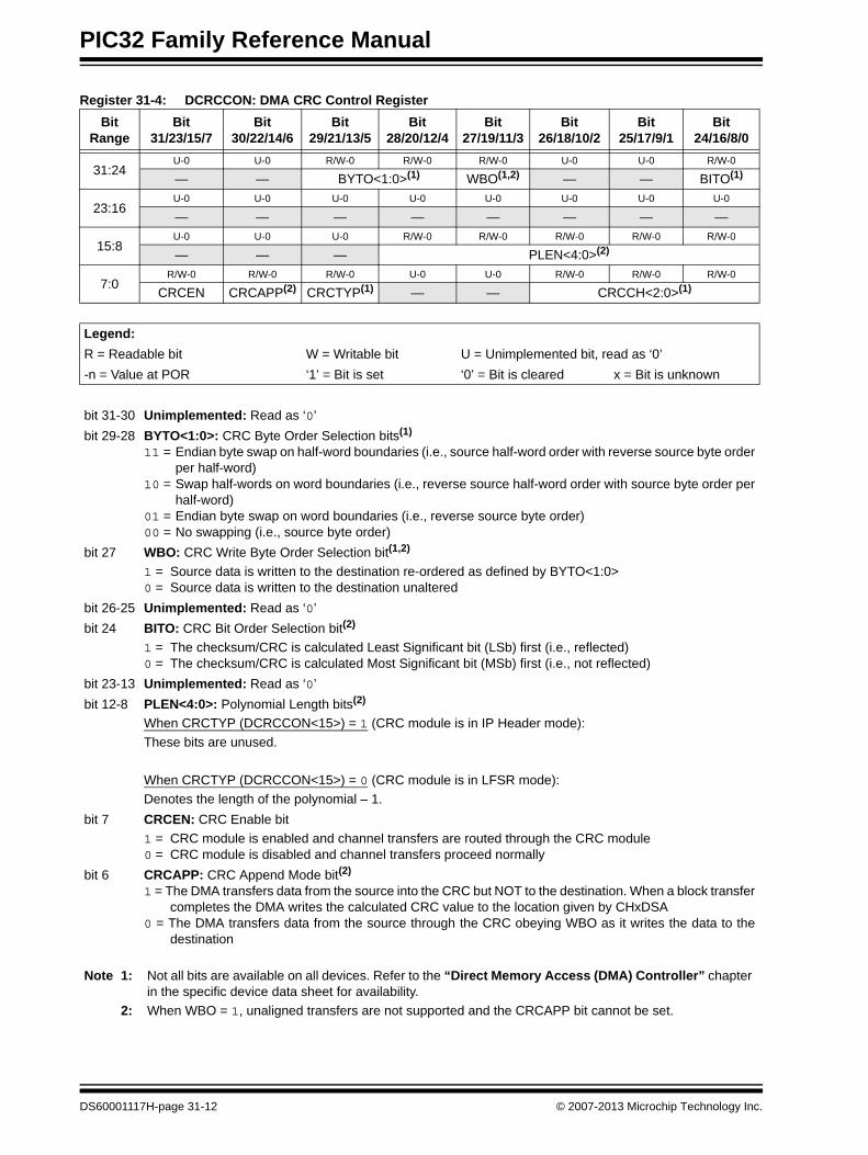
Register 31-4: DCRCCON: DMA CRC Control Register
Bit Range
Bit31/23/15/7
Bit30/22/14/6
Bit29/21/13/5
Bit28/20/12/4
Bit27/19/11/3
Bit26/18/10/2
Bit25/17/9/1
Bit24/16/8/0
31:24U-0 U-0 R/W-0 R/W-0 R/W-0 U-0 U-0 R/W-0
— — BYTO<1:0>(1) WBO(1,2) — — BITO(1)
23:16U-0 U-0 U-0 U-0 U-0 U-0 U-0 U-0
— — — — — — — —
15:8U-0 U-0 U-0 R/W-0 R/W-0 R/W-0 R/W-0 R/W-0
— — — PLEN<4:0>(2)
7:0R/W-0 R/W-0 R/W-0 U-0 U-0 R/W-0 R/W-0 R/W-0
CRCEN CRCAPP(2) CRCTYP(1) — — CRCCH<2:0>(1)
Legend:
R = Readable bit W = Writable bit U = Unimplemented bit, read as ‘0’
-n = Value at POR ‘1’ = Bit is set ‘0’ = Bit is cleared x = Bit is unknown
bit 31-30 Unimplemented: Read as ‘0’
bit 29-28 BYTO<1:0>: CRC Byte Order Selection bits(1)
11 = Endian byte swap on half-word boundaries (i.e., source half-word order with reverse source byte orderper half-word)
10 = Swap half-words on word boundaries (i.e., reverse source half-word order with source byte order perhalf-word)
01 = Endian byte swap on word boundaries (i.e., reverse source byte order)00 = No swapping (i.e., source byte order)
bit 27 WBO: CRC Write Byte Order Selection bit(1,2)
1 = Source data is written to the destination re-ordered as defined by BYTO<1:0>0 = Source data is written to the destination unaltered
bit 26-25 Unimplemented: Read as ‘0’
bit 24 BITO: CRC Bit Order Selection bit(2)
1 = The checksum/CRC is calculated Least Significant bit (LSb) first (i.e., reflected)0 = The checksum/CRC is calculated Most Significant bit (MSb) first (i.e., not reflected)
bit 23-13 Unimplemented: Read as ‘0’
bit 12-8 PLEN<4:0>: Polynomial Length bits(2)
When CRCTYP (DCRCCON<15>) = 1 (CRC module is in IP Header mode):
These bits are unused.
When CRCTYP (DCRCCON<15>) = 0 (CRC module is in LFSR mode):
Denotes the length of the polynomial – 1.
bit 7 CRCEN: CRC Enable bit
1 = CRC module is enabled and channel transfers are routed through the CRC module0 = CRC module is disabled and channel transfers proceed normally
bit 6 CRCAPP: CRC Append Mode bit(2)
1 = The DMA transfers data from the source into the CRC but NOT to the destination. When a block transfercompletes the DMA writes the calculated CRC value to the location given by CHxDSA
0 = The DMA transfers data from the source through the CRC obeying WBO as it writes the data to thedestination
Note 1: Not all bits are available on all devices. Refer to the “Direct Memory Access (DMA) Controller” chapter in the specific device data sheet for availability.
2: When WBO = 1, unaligned transfers are not supported and the CRCAPP bit cannot be set.
DS60001117H-page 31-12 © 2007-2013 Microchip Technology Inc.
Section 31. DMA ControllerD
MA
Co
ntro
ller
31
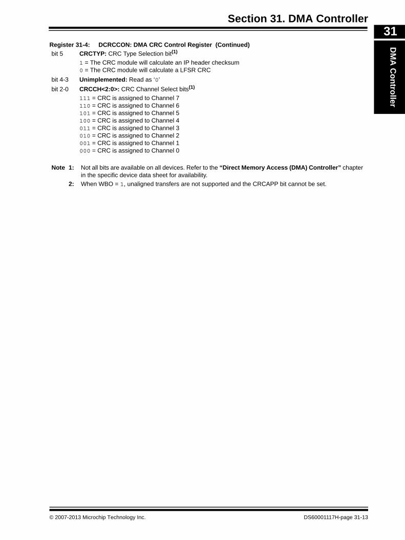
bit 5 CRCTYP: CRC Type Selection bit(1)
1 = The CRC module will calculate an IP header checksum0 = The CRC module will calculate a LFSR CRC
bit 4-3 Unimplemented: Read as ‘0’
bit 2-0 CRCCH<2:0>: CRC Channel Select bits(1)
111 = CRC is assigned to Channel 7110 = CRC is assigned to Channel 6101 = CRC is assigned to Channel 5100 = CRC is assigned to Channel 4011 = CRC is assigned to Channel 3010 = CRC is assigned to Channel 2001 = CRC is assigned to Channel 1000 = CRC is assigned to Channel 0
Register 31-4: DCRCCON: DMA CRC Control Register (Continued)
Note 1: Not all bits are available on all devices. Refer to the “Direct Memory Access (DMA) Controller” chapter in the specific device data sheet for availability.
2: When WBO = 1, unaligned transfers are not supported and the CRCAPP bit cannot be set.
© 2007-2013 Microchip Technology Inc. DS60001117H-page 31-13
PIC32 Family Reference Manual
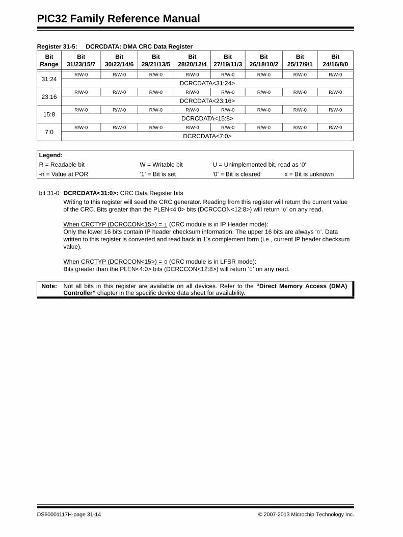
Register 31-5: DCRCDATA: DMA CRC Data Register
Bit Range
Bit31/23/15/7
Bit30/22/14/6
Bit29/21/13/5
Bit28/20/12/4
Bit27/19/11/3
Bit26/18/10/2
Bit25/17/9/1
Bit24/16/8/0
31:24R/W-0 R/W-0 R/W-0 R/W-0 R/W-0 R/W-0 R/W-0 R/W-0
DCRCDATA<31:24>
23:16R/W-0 R/W-0 R/W-0 R/W-0 R/W-0 R/W-0 R/W-0 R/W-0
DCRCDATA<23:16>
15:8R/W-0 R/W-0 R/W-0 R/W-0 R/W-0 R/W-0 R/W-0 R/W-0
DCRCDATA<15:8>
7:0R/W-0 R/W-0 R/W-0 R/W-0 R/W-0 R/W-0 R/W-0 R/W-0
DCRCDATA<7:0>
Legend:
R = Readable bit W = Writable bit U = Unimplemented bit, read as ‘0’
-n = Value at POR ‘1’ = Bit is set ‘0’ = Bit is cleared x = Bit is unknown
bit 31-0 DCRCDATA<31:0>: CRC Data Register bits
Writing to this register will seed the CRC generator. Reading from this register will return the current value of the CRC. Bits greater than the PLEN<4:0> bits (DCRCCON<12:8>) will return ‘0’ on any read.
When CRCTYP (DCRCCON<15>) = 1 (CRC module is in IP Header mode):Only the lower 16 bits contain IP header checksum information. The upper 16 bits are always ‘0’. Data written to this register is converted and read back in 1’s complement form (i.e., current IP header checksum value).
When CRCTYP (DCRCCON<15>) = 0 (CRC module is in LFSR mode):Bits greater than the PLEN<4:0> bits (DCRCCON<12:8>) will return ‘0’ on any read.
Note: Not all bits in this register are available on all devices. Refer to the “Direct Memory Access (DMA)Controller” chapter in the specific device data sheet for availability.
DS60001117H-page 31-14 © 2007-2013 Microchip Technology Inc.

Section 31. DMA ControllerD
MA
Co
ntro
ller
31
Register 31-6: DCRCXOR: DMA CRCXOR Enable RegisterBit Range
Bit31/23/15/7
Bit30/22/14/6
Bit29/21/13/5
Bit28/20/12/4
Bit27/19/11/3
Bit26/18/10/2
Bit25/17/9/1
Bit24/16/8/0
31:24R/W-0 R/W-0 R/W-0 R/W-0 R/W-0 R/W-0 R/W-0 R/W-0
DCRCXOR<31:24>
23:16R/W-0 R/W-0 R/W-0 R/W-0 R/W-0 R/W-0 R/W-0 R/W-0
DCRCXOR<23:16>
15:8R/W-0 R/W-0 R/W-0 R/W-0 R/W-0 R/W-0 R/W-0 R/W-0
DCRCXOR<15:8>
7:0R/W-0 R/W-0 R/W-0 R/W-0 R/W-0 R/W-0 R/W-0 R/W-0
DCRCXOR<7:0>
Legend:
R = Readable bit W = Writable bit U = Unimplemented bit, read as ‘0’
-n = Value at POR ‘1’ = Bit is set ‘0’ = Bit is cleared x = Bit is unknown
bit 31-0 DCRCXOR<31:0>: CRC XOR Register bits
When CRCTYP (DCRCCON<15>) = 1 (CRC module is in IP Header mode):This register is unused.
When CRCTYP (DCRCCON<15>) = 0 (CRC module is in LFSR mode):1 = Enable the XOR input to the Shift register0 = Disable the XOR input to the Shift register; data is shifted in directly from the previous stage in
the register
Note: Not all bits in this register are available on all devices. Refer to the “Direct Memory Access (DMA)Controller” chapter in the specific device data sheet for availability.
© 2007-2013 Microchip Technology Inc. DS60001117H-page 31-15
PIC32 Family Reference Manual
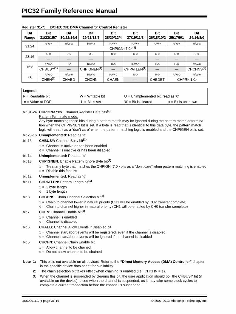
Register 31-7: DCHxCON: DMA Channel ‘x’ Control Register
Bit Range
Bit31/23/15/7
Bit30/22/14/6
Bit29/21/13/5
Bit28/20/12/4
Bit27/19/11/3
Bit26/18/10/2
Bit25/17/9/1
Bit24/16/8/0
31:24R/W-x R/W-x R/W-x R/W-x R/W-x R/W-x R/W-x R/W-x
CHPIGN<7:0>(1)
23:16U-0 U-0 U-0 U-0 U-0 U-0 U-0 U-0
— — — — — — — —
15:8R/W-0 U-0 R/W-0 U-0 R/W-0 U-0 U-0 R/W-0
CHBUSY(1) — CHPIGNEN(1) — CHPATLEN(1) — — CHCHNS(2)
7:0R/W-0 R/W-0 R/W-0 R/W-0 U-0 R-0 R/W-0 R/W-0
CHEN(3) CHAED CHCHN CHAEN — CHEDET CHPRI<1:0>
Legend:
R = Readable bit W = Writable bit U = Unimplemented bit, read as ‘0’
-n = Value at POR ‘1’ = Bit is set ‘0’ = Bit is cleared x = Bit is unknown
bit 31-24 CHPIGN<7:0>: Channel Register Data bits(1)
Pattern Terminate mode:Any byte matching these bits during a pattern match may be ignored during the pattern match determina-tion when the CHPIGNEN bit is set. If a byte is read that is identical to this data byte, the pattern match logic will treat it as a “don’t care” when the pattern matching logic is enabled and the CHPIGEN bit is set.
bit 23-16 Unimplemented: Read as ‘0’
bit 15 CHBUSY: Channel Busy bit(1)
1 = Channel is active or has been enabled0 = Channel is inactive or has been disabled
bit 14 Unimplemented: Read as ‘0’
bit 13 CHPIGNEN: Enable Pattern Ignore Byte bit(1)
1 = Treat any byte that matches the CHPIGN<7:0> bits as a “don’t care” when pattern matching is enabled0 = Disable this feature
bit 12 Unimplemented: Read as ‘0’
bit 11 CHPATLEN: Pattern Length bit(1)
1 = 2 byte length0 = 1 byte length
bit 8 CHCHNS: Chain Channel Selection bit(2)
1 = Chain to channel lower in natural priority (CH1 will be enabled by CH2 transfer complete)0 = Chain to channel higher in natural priority (CH1 will be enabled by CH0 transfer complete)
bit 7 CHEN: Channel Enable bit(3)
1 = Channel is enabled0 = Channel is disabled
bit 6 CHAED: Channel Allow Events If Disabled bit
1 = Channel start/abort events will be registered, even if the channel is disabled0 = Channel start/abort events will be ignored if the channel is disabled
bit 5 CHCHN: Channel Chain Enable bit
1 = Allow channel to be chained0 = Do not allow channel to be chained
Note 1: This bit is not available on all devices. Refer to the “Direct Memory Access (DMA) Controller” chapter in the specific device data sheet for availability.
2: The chain selection bit takes effect when chaining is enabled (i.e., CHCHN = 1).
3: When the channel is suspended by clearing this bit, the user application should poll the CHBUSY bit (if available on the device) to see when the channel is suspended, as it may take some clock cycles to complete a current transaction before the channel is suspended.
DS60001117H-page 31-16 © 2007-2013 Microchip Technology Inc.
Section 31. DMA ControllerD
MA
Co
ntro
ller
31
bit 4 CHAEN: Channel Automatic Enable bit
1 = Channel is continuously enabled, and not automatically disabled after a block transfer is complete0 = Channel is disabled on block transfer complete
bit 3 Unimplemented: Read as ‘0’
bit 2 CHEDET: Channel Event Detected bit
1 = An event has been detected0 = No events have been detected
bit 1-0 CHPRI<1:0>: Channel Priority bits
11 = Channel has priority 3 (highest)10 = Channel has priority 201 = Channel has priority 100 = Channel has priority 0
Register 31-7: DCHxCON: DMA Channel ‘x’ Control Register (Continued)
Note 1: This bit is not available on all devices. Refer to the “Direct Memory Access (DMA) Controller” chapter in the specific device data sheet for availability.
2: The chain selection bit takes effect when chaining is enabled (i.e., CHCHN = 1).
3: When the channel is suspended by clearing this bit, the user application should poll the CHBUSY bit (if available on the device) to see when the channel is suspended, as it may take some clock cycles to complete a current transaction before the channel is suspended.
© 2007-2013 Microchip Technology Inc. DS60001117H-page 31-17
PIC32 Family Reference Manual
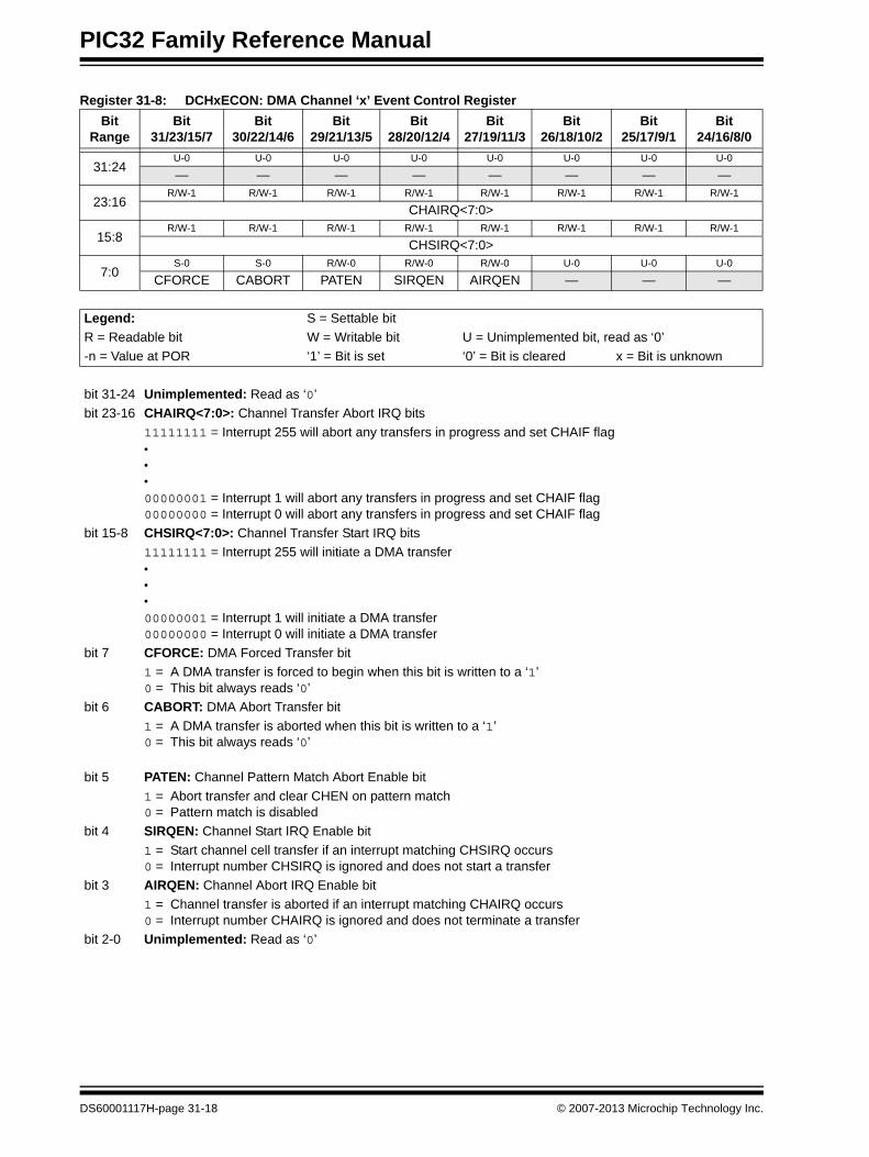
Register 31-8: DCHxECON: DMA Channel ‘x’ Event Control Register
Bit Range
Bit31/23/15/7
Bit30/22/14/6
Bit29/21/13/5
Bit28/20/12/4
Bit27/19/11/3
Bit26/18/10/2
Bit25/17/9/1
Bit24/16/8/0
31:24U-0 U-0 U-0 U-0 U-0 U-0 U-0 U-0
— — — — — — — —
23:16R/W-1 R/W-1 R/W-1 R/W-1 R/W-1 R/W-1 R/W-1 R/W-1
CHAIRQ<7:0>
15:8R/W-1 R/W-1 R/W-1 R/W-1 R/W-1 R/W-1 R/W-1 R/W-1
CHSIRQ<7:0>
7:0S-0 S-0 R/W-0 R/W-0 R/W-0 U-0 U-0 U-0
CFORCE CABORT PATEN SIRQEN AIRQEN — — —
Legend: S = Settable bit
R = Readable bit W = Writable bit U = Unimplemented bit, read as ‘0’
-n = Value at POR ‘1’ = Bit is set ‘0’ = Bit is cleared x = Bit is unknown
bit 31-24 Unimplemented: Read as ‘0’
bit 23-16 CHAIRQ<7:0>: Channel Transfer Abort IRQ bits
11111111 = Interrupt 255 will abort any transfers in progress and set CHAIF flag•••
00000001 = Interrupt 1 will abort any transfers in progress and set CHAIF flag00000000 = Interrupt 0 will abort any transfers in progress and set CHAIF flag
bit 15-8 CHSIRQ<7:0>: Channel Transfer Start IRQ bits
11111111 = Interrupt 255 will initiate a DMA transfer•••
00000001 = Interrupt 1 will initiate a DMA transfer00000000 = Interrupt 0 will initiate a DMA transfer
bit 7 CFORCE: DMA Forced Transfer bit
1 = A DMA transfer is forced to begin when this bit is written to a ‘1’0 = This bit always reads ‘0’
bit 6 CABORT: DMA Abort Transfer bit
1 = A DMA transfer is aborted when this bit is written to a ‘1’0 = This bit always reads ‘0’
bit 5 PATEN: Channel Pattern Match Abort Enable bit
1 = Abort transfer and clear CHEN on pattern match0 = Pattern match is disabled
bit 4 SIRQEN: Channel Start IRQ Enable bit
1 = Start channel cell transfer if an interrupt matching CHSIRQ occurs0 = Interrupt number CHSIRQ is ignored and does not start a transfer
bit 3 AIRQEN: Channel Abort IRQ Enable bit
1 = Channel transfer is aborted if an interrupt matching CHAIRQ occurs0 = Interrupt number CHAIRQ is ignored and does not terminate a transfer
bit 2-0 Unimplemented: Read as ‘0’
DS60001117H-page 31-18 © 2007-2013 Microchip Technology Inc.
Section 31. DMA ControllerD
MA
Co
ntro
ller
31
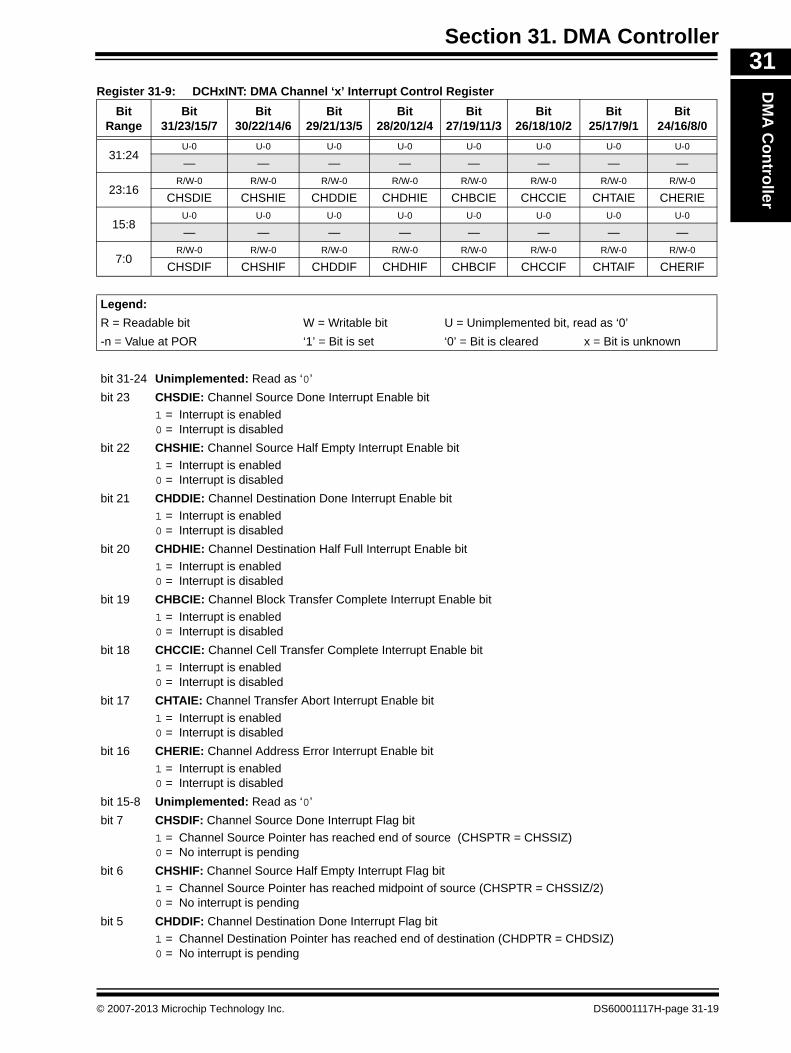
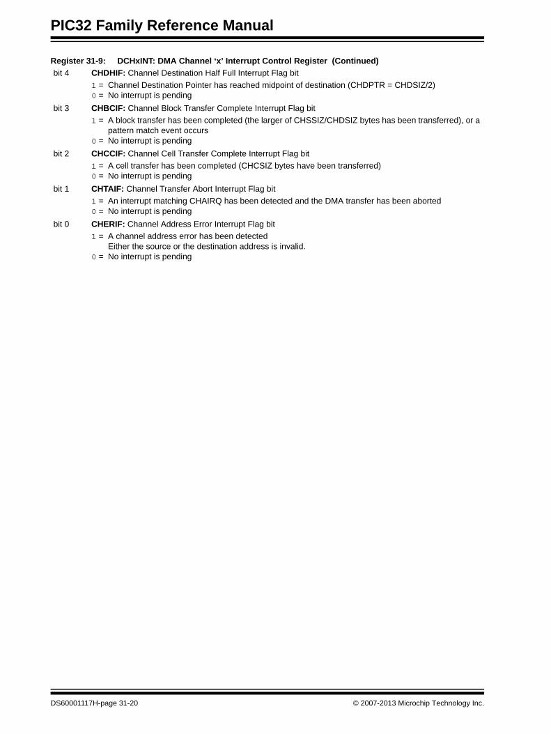
Register 31-9: DCHxINT: DMA Channel ‘x’ Interrupt Control RegisterBit Range
Bit31/23/15/7
Bit30/22/14/6
Bit29/21/13/5
Bit28/20/12/4
Bit27/19/11/3
Bit26/18/10/2
Bit25/17/9/1
Bit24/16/8/0
31:24U-0 U-0 U-0 U-0 U-0 U-0 U-0 U-0
— — — — — — — —
23:16R/W-0 R/W-0 R/W-0 R/W-0 R/W-0 R/W-0 R/W-0 R/W-0
CHSDIE CHSHIE CHDDIE CHDHIE CHBCIE CHCCIE CHTAIE CHERIE
15:8U-0 U-0 U-0 U-0 U-0 U-0 U-0 U-0
— — — — — — — —
7:0R/W-0 R/W-0 R/W-0 R/W-0 R/W-0 R/W-0 R/W-0 R/W-0
CHSDIF CHSHIF CHDDIF CHDHIF CHBCIF CHCCIF CHTAIF CHERIF
Legend:
R = Readable bit W = Writable bit U = Unimplemented bit, read as ‘0’
-n = Value at POR ‘1’ = Bit is set ‘0’ = Bit is cleared x = Bit is unknown
bit 31-24 Unimplemented: Read as ‘0’
bit 23 CHSDIE: Channel Source Done Interrupt Enable bit
1 = Interrupt is enabled0 = Interrupt is disabled
bit 22 CHSHIE: Channel Source Half Empty Interrupt Enable bit
1 = Interrupt is enabled0 = Interrupt is disabled
bit 21 CHDDIE: Channel Destination Done Interrupt Enable bit
1 = Interrupt is enabled0 = Interrupt is disabled
bit 20 CHDHIE: Channel Destination Half Full Interrupt Enable bit
1 = Interrupt is enabled0 = Interrupt is disabled
bit 19 CHBCIE: Channel Block Transfer Complete Interrupt Enable bit
1 = Interrupt is enabled0 = Interrupt is disabled
bit 18 CHCCIE: Channel Cell Transfer Complete Interrupt Enable bit
1 = Interrupt is enabled0 = Interrupt is disabled
bit 17 CHTAIE: Channel Transfer Abort Interrupt Enable bit
1 = Interrupt is enabled0 = Interrupt is disabled
bit 16 CHERIE: Channel Address Error Interrupt Enable bit
1 = Interrupt is enabled0 = Interrupt is disabled
bit 15-8 Unimplemented: Read as ‘0’
bit 7 CHSDIF: Channel Source Done Interrupt Flag bit
1 = Channel Source Pointer has reached end of source (CHSPTR = CHSSIZ)0 = No interrupt is pending
bit 6 CHSHIF: Channel Source Half Empty Interrupt Flag bit
1 = Channel Source Pointer has reached midpoint of source (CHSPTR = CHSSIZ/2) 0 = No interrupt is pending
bit 5 CHDDIF: Channel Destination Done Interrupt Flag bit
1 = Channel Destination Pointer has reached end of destination (CHDPTR = CHDSIZ) 0 = No interrupt is pending
© 2007-2013 Microchip Technology Inc. DS60001117H-page 31-19
PIC32 Family Reference Manual
bit 4 CHDHIF: Channel Destination Half Full Interrupt Flag bit
1 = Channel Destination Pointer has reached midpoint of destination (CHDPTR = CHDSIZ/2) 0 = No interrupt is pending
bit 3 CHBCIF: Channel Block Transfer Complete Interrupt Flag bit
1 = A block transfer has been completed (the larger of CHSSIZ/CHDSIZ bytes has been transferred), or apattern match event occurs
0 = No interrupt is pending
bit 2 CHCCIF: Channel Cell Transfer Complete Interrupt Flag bit
1 = A cell transfer has been completed (CHCSIZ bytes have been transferred) 0 = No interrupt is pending
bit 1 CHTAIF: Channel Transfer Abort Interrupt Flag bit
1 = An interrupt matching CHAIRQ has been detected and the DMA transfer has been aborted 0 = No interrupt is pending
bit 0 CHERIF: Channel Address Error Interrupt Flag bit
1 = A channel address error has been detected Either the source or the destination address is invalid.
0 = No interrupt is pending
Register 31-9: DCHxINT: DMA Channel ‘x’ Interrupt Control Register (Continued)
DS60001117H-page 31-20 © 2007-2013 Microchip Technology Inc.
Section 31. DMA ControllerD
MA
Co
ntro
ller
31
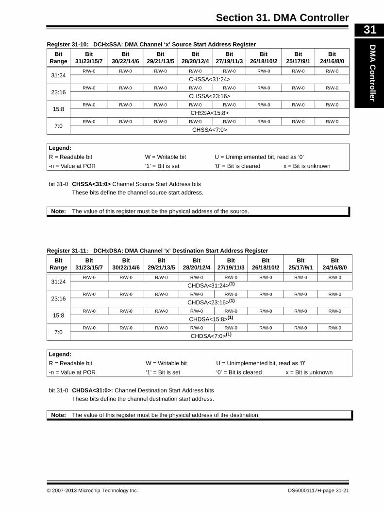
Register 31-10: DCHxSSA: DMA Channel ‘x’ Source Start Address RegisterBit Range
Bit31/23/15/7
Bit30/22/14/6
Bit29/21/13/5
Bit28/20/12/4
Bit27/19/11/3
Bit26/18/10/2
Bit25/17/9/1
Bit24/16/8/0
31:24R/W-0 R/W-0 R/W-0 R/W-0 R/W-0 R/W-0 R/W-0 R/W-0
CHSSA<31:24>
23:16R/W-0 R/W-0 R/W-0 R/W-0 R/W-0 R/W-0 R/W-0 R/W-0
CHSSA<23:16>
15:8R/W-0 R/W-0 R/W-0 R/W-0 R/W-0 R/W-0 R/W-0 R/W-0
CHSSA<15:8>
7:0R/W-0 R/W-0 R/W-0 R/W-0 R/W-0 R/W-0 R/W-0 R/W-0
CHSSA<7:0>
Legend:
R = Readable bit W = Writable bit U = Unimplemented bit, read as ‘0’
-n = Value at POR ‘1’ = Bit is set ‘0’ = Bit is cleared x = Bit is unknown
bit 31-0 CHSSA<31:0> Channel Source Start Address bits
These bits define the channel source start address.
Note: The value of this register must be the physical address of the source.
Register 31-11: DCHxDSA: DMA Channel ‘x’ Destination Start Address Register
Bit Range
Bit31/23/15/7
Bit30/22/14/6
Bit29/21/13/5
Bit28/20/12/4
Bit27/19/11/3
Bit26/18/10/2
Bit25/17/9/1
Bit24/16/8/0
31:24R/W-0 R/W-0 R/W-0 R/W-0 R/W-0 R/W-0 R/W-0 R/W-0
CHDSA<31:24>(1)
23:16R/W-0 R/W-0 R/W-0 R/W-0 R/W-0 R/W-0 R/W-0 R/W-0
CHDSA<23:16>(1)
15:8R/W-0 R/W-0 R/W-0 R/W-0 R/W-0 R/W-0 R/W-0 R/W-0
CHDSA<15:8>(1)
7:0R/W-0 R/W-0 R/W-0 R/W-0 R/W-0 R/W-0 R/W-0 R/W-0
CHDSA<7:0>(1)
Legend:
R = Readable bit W = Writable bit U = Unimplemented bit, read as ‘0’
-n = Value at POR ‘1’ = Bit is set ‘0’ = Bit is cleared x = Bit is unknown
bit 31-0 CHDSA<31:0>: Channel Destination Start Address bits
These bits define the channel destination start address.
Note: The value of this register must be the physical address of the destination.
© 2007-2013 Microchip Technology Inc. DS60001117H-page 31-21
PIC32 Family Reference Manual
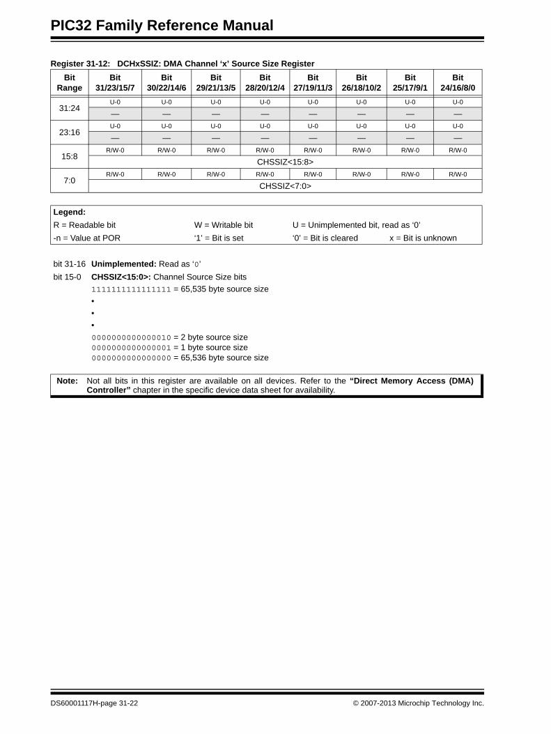
Register 31-12: DCHxSSIZ: DMA Channel ‘x’ Source Size Register
Bit Range
Bit31/23/15/7
Bit30/22/14/6
Bit29/21/13/5
Bit28/20/12/4
Bit27/19/11/3
Bit26/18/10/2
Bit25/17/9/1
Bit24/16/8/0
31:24U-0 U-0 U-0 U-0 U-0 U-0 U-0 U-0
— — — — — — — —
23:16U-0 U-0 U-0 U-0 U-0 U-0 U-0 U-0
— — — — — — — —
15:8R/W-0 R/W-0 R/W-0 R/W-0 R/W-0 R/W-0 R/W-0 R/W-0
CHSSIZ<15:8>
7:0R/W-0 R/W-0 R/W-0 R/W-0 R/W-0 R/W-0 R/W-0 R/W-0
CHSSIZ<7:0>
Legend:
R = Readable bit W = Writable bit U = Unimplemented bit, read as ‘0’
-n = Value at POR ‘1’ = Bit is set ‘0’ = Bit is cleared x = Bit is unknown
bit 31-16 Unimplemented: Read as ‘0’
bit 15-0 CHSSIZ<15:0>: Channel Source Size bits
1111111111111111 = 65,535 byte source size
•
•
•
0000000000000010 = 2 byte source size0000000000000001 = 1 byte source size0000000000000000 = 65,536 byte source size
Note: Not all bits in this register are available on all devices. Refer to the “Direct Memory Access (DMA)Controller” chapter in the specific device data sheet for availability.
DS60001117H-page 31-22 © 2007-2013 Microchip Technology Inc.

Section 31. DMA ControllerD
MA
Co
ntro
ller
31
Register 31-13: DCHxDSIZ: DMA Channel ‘x’ Destination Size RegisterBit Range
Bit31/23/15/7
Bit30/22/14/6
Bit29/21/13/5
Bit28/20/12/4
Bit27/19/11/3
Bit26/18/10/2
Bit25/17/9/1
Bit24/16/8/0
31:24U-0 U-0 U-0 U-0 U-0 U-0 U-0 U-0
— — — — — — — —
23:16U-0 U-0 U-0 U-0 U-0 U-0 U-0 U-0
— — — — — — — —
15:8R/W-0 R/W-0 R/W-0 R/W-0 R/W-0 R/W-0 R/W-0 R/W-0
CHDSIZ<15:8>
7:0R/W-0 R/W-0 R/W-0 R/W-0 R/W-0 R/W-0 R/W-0 R/W-0
CHDSIZ<7:0>
Legend:
R = Readable bit W = Writable bit U = Unimplemented bit, read as ‘0’
-n = Value at POR ‘1’ = Bit is set ‘0’ = Bit is cleared x = Bit is unknown
bit 31-16 Unimplemented: Read as ‘0’
bit 15-0 CHDSIZ<15:0>: Channel Destination Size bits
1111111111111111 = 65,535 byte destination size
•
•
•
0000000000000010 = 2 byte destination size0000000000000001 = 1 byte destination size0000000000000000 = 65,536 byte destination size
Note: Not all bits in this register are available on all devices. Refer to the “Direct Memory Access (DMA)Controller” chapter in the specific device data sheet for availability.
© 2007-2013 Microchip Technology Inc. DS60001117H-page 31-23
PIC32 Family Reference Manual
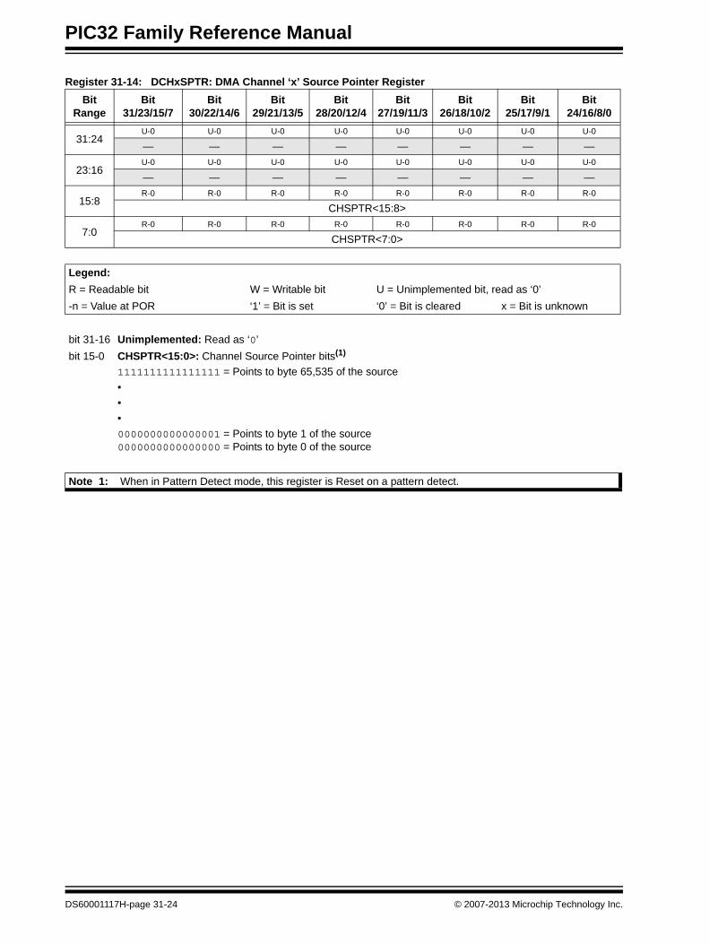
Register 31-14: DCHxSPTR: DMA Channel ‘x’ Source Pointer Register
Bit Range
Bit31/23/15/7
Bit30/22/14/6
Bit29/21/13/5
Bit28/20/12/4
Bit27/19/11/3
Bit26/18/10/2
Bit25/17/9/1
Bit24/16/8/0
31:24U-0 U-0 U-0 U-0 U-0 U-0 U-0 U-0
— — — — — — — —
23:16U-0 U-0 U-0 U-0 U-0 U-0 U-0 U-0
— — — — — — — —
15:8R-0 R-0 R-0 R-0 R-0 R-0 R-0 R-0
CHSPTR<15:8>
7:0R-0 R-0 R-0 R-0 R-0 R-0 R-0 R-0
CHSPTR<7:0>
Legend:
R = Readable bit W = Writable bit U = Unimplemented bit, read as ‘0’
-n = Value at POR ‘1’ = Bit is set ‘0’ = Bit is cleared x = Bit is unknown
bit 31-16 Unimplemented: Read as ‘0’
bit 15-0 CHSPTR<15:0>: Channel Source Pointer bits(1)
1111111111111111 = Points to byte 65,535 of the source
•
•
•
0000000000000001 = Points to byte 1 of the source0000000000000000 = Points to byte 0 of the source
Note 1: When in Pattern Detect mode, this register is Reset on a pattern detect.
DS60001117H-page 31-24 © 2007-2013 Microchip Technology Inc.
Section 31. DMA ControllerD
MA
Co
ntro
ller
31
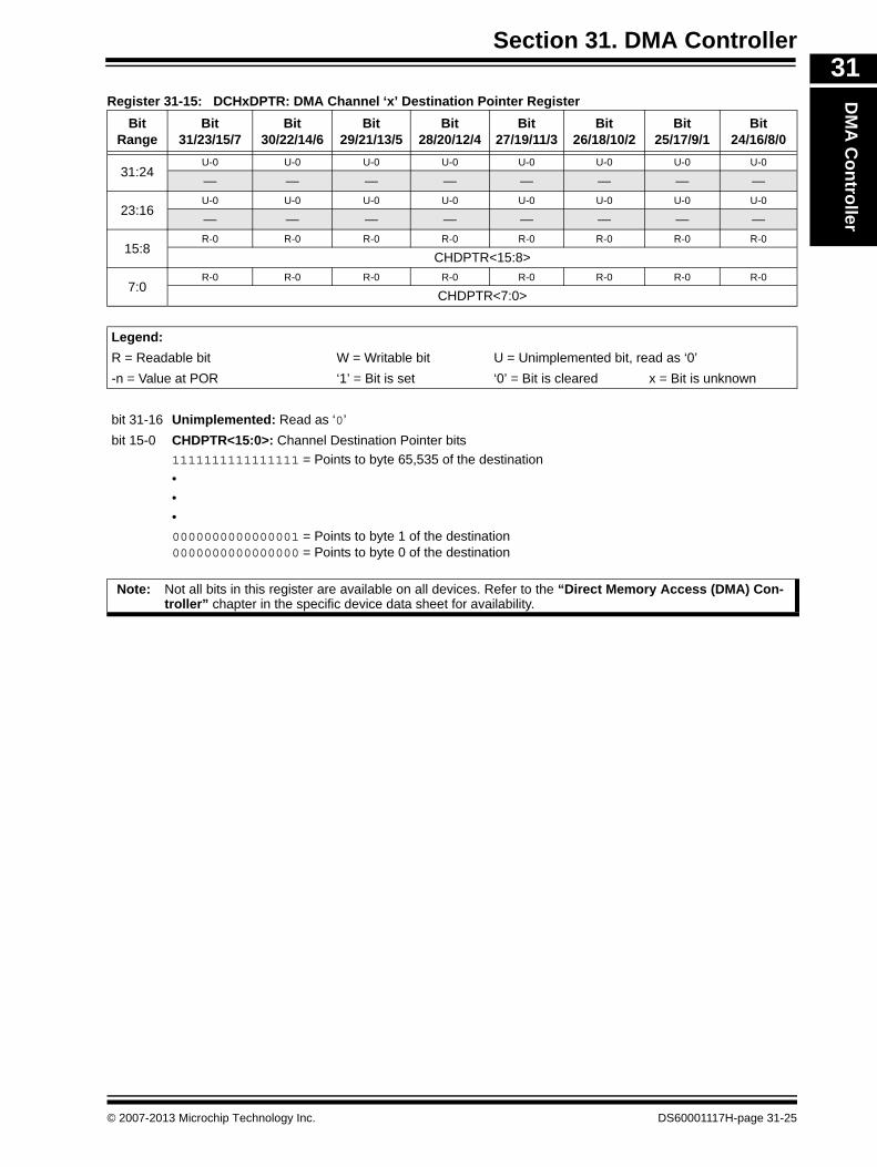
Register 31-15: DCHxDPTR: DMA Channel ‘x’ Destination Pointer Register
Bit Range
Bit31/23/15/7
Bit30/22/14/6
Bit29/21/13/5
Bit28/20/12/4
Bit27/19/11/3
Bit26/18/10/2
Bit25/17/9/1
Bit24/16/8/0
31:24U-0 U-0 U-0 U-0 U-0 U-0 U-0 U-0
— — — — — — — —
23:16U-0 U-0 U-0 U-0 U-0 U-0 U-0 U-0
— — — — — — — —
15:8R-0 R-0 R-0 R-0 R-0 R-0 R-0 R-0
CHDPTR<15:8>
7:0R-0 R-0 R-0 R-0 R-0 R-0 R-0 R-0
CHDPTR<7:0>
Legend:
R = Readable bit W = Writable bit U = Unimplemented bit, read as ‘0’
-n = Value at POR ‘1’ = Bit is set ‘0’ = Bit is cleared x = Bit is unknown
bit 31-16 Unimplemented: Read as ‘0’
bit 15-0 CHDPTR<15:0>: Channel Destination Pointer bits
1111111111111111 = Points to byte 65,535 of the destination
•
•
•
0000000000000001 = Points to byte 1 of the destination0000000000000000 = Points to byte 0 of the destination
Note: Not all bits in this register are available on all devices. Refer to the “Direct Memory Access (DMA) Con-troller” chapter in the specific device data sheet for availability.
© 2007-2013 Microchip Technology Inc. DS60001117H-page 31-25
PIC32 Family Reference Manual
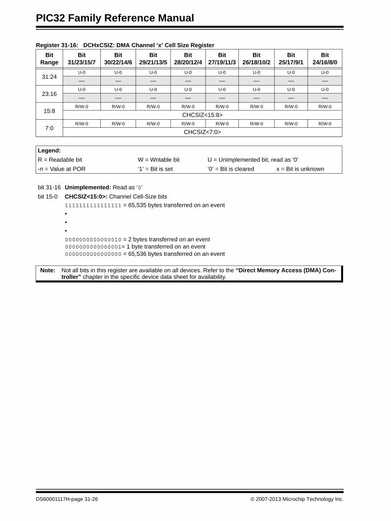
Register 31-16: DCHxCSIZ: DMA Channel ‘x’ Cell Size Register
Bit Range
Bit31/23/15/7
Bit30/22/14/6
Bit29/21/13/5
Bit28/20/12/4
Bit27/19/11/3
Bit26/18/10/2
Bit25/17/9/1
Bit24/16/8/0
31:24U-0 U-0 U-0 U-0 U-0 U-0 U-0 U-0
— — — — — — — —
23:16U-0 U-0 U-0 U-0 U-0 U-0 U-0 U-0
— — — — — — — —
15:8R/W-0 R/W-0 R/W-0 R/W-0 R/W-0 R/W-0 R/W-0 R/W-0
CHCSIZ<15:8>
7:0R/W-0 R/W-0 R/W-0 R/W-0 R/W-0 R/W-0 R/W-0 R/W-0
CHCSIZ<7:0>
Legend:
R = Readable bit W = Writable bit U = Unimplemented bit, read as ‘0’
-n = Value at POR ‘1’ = Bit is set ‘0’ = Bit is cleared x = Bit is unknown
bit 31-16 Unimplemented: Read as ‘0’
bit 15-0 CHCSIZ<15:0>: Channel Cell-Size bits
1111111111111111 = 65,535 bytes transferred on an event
•
•
•
0000000000000010 = 2 bytes transferred on an event0000000000000001= 1 byte transferred on an event0000000000000000 = 65,536 bytes transferred on an event
Note: Not all bits in this register are available on all devices. Refer to the “Direct Memory Access (DMA) Con-troller” chapter in the specific device data sheet for availability.
DS60001117H-page 31-26 © 2007-2013 Microchip Technology Inc.

Section 31. DMA ControllerD
MA
Co
ntro
ller
31
Register 31-17: DCHxCPTR: DMA Channel ‘x’ Cell Pointer RegisterBit Range
Bit31/23/15/7
Bit30/22/14/6
Bit29/21/13/5
Bit28/20/12/4
Bit27/19/11/3
Bit26/18/10/2
Bit25/17/9/1
Bit24/16/8/0
31:24U-0 U-0 U-0 U-0 U-0 U-0 U-0 U-0
— — — — — — — —
23:16U-0 U-0 U-0 U-0 U-0 U-0 U-0 U-0
— — — — — — — —
15:8R-0 R-0 R-0 R-0 R-0 R-0 R-0 R-0
CHCPTR<15:8>
7:0R-0 R-0 R-0 R-0 R-0 R-0 R-0 R-0
CHCPTR<7:0>
Legend:
R = Readable bit W = Writable bit U = Unimplemented bit, read as ‘0’
-n = Value at POR ‘1’ = Bit is set ‘0’ = Bit is cleared x = Bit is unknown
bit 31-16 Unimplemented: Read as ‘0’
bit 15-0 CHCPTR<15:0>: Channel Cell Progress Pointer bits1111111111111111 = 65,535 bytes have been transferred since the last event•••
0000000000000001 = 1 byte has been transferred since the last event0000000000000000 = 0 bytes have been transferred since the last event
Note 1: Not all bits in this register are available on all devices. Refer to the “Direct Memory Access (DMA) Controller” chapter in the specific device data sheet for availability.
2: When in Pattern Detect mode, this register is Reset on a pattern detect.
© 2007-2013 Microchip Technology Inc. DS60001117H-page 31-27
PIC32 Family Reference Manual
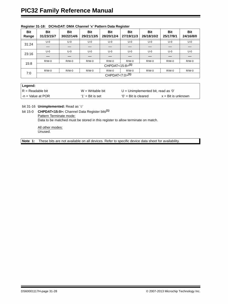
Register 31-18: DCHxDAT: DMA Channel ‘x’ Pattern Data Register
Bit Range
Bit31/23/15/7
Bit30/22/14/6
Bit29/21/13/5
Bit28/20/12/4
Bit27/19/11/3
Bit26/18/10/2
Bit25/17/9/1
Bit24/16/8/0
31:24U-0 U-0 U-0 U-0 U-0 U-0 U-0 U-0
— — — — — — — —
23:16U-0 U-0 U-0 U-0 U-0 U-0 U-0 U-0
— — — — — — — —
15:8R/W-0 R/W-0 R/W-0 R/W-0 R/W-0 R/W-0 R/W-0 R/W-0
CHPDAT<15:8>(1)
7:0R/W-0 R/W-0 R/W-0 R/W-0 R/W-0 R/W-0 R/W-0 R/W-0
CHPDAT<7:0>(1)
Legend:
R = Readable bit W = Writable bit U = Unimplemented bit, read as ‘0’
-n = Value at POR ‘1’ = Bit is set ‘0’ = Bit is cleared x = Bit is unknown
bit 31-16 Unimplemented: Read as ‘0’
bit 15-0 CHPDAT<15:0>: Channel Data Register bits(1)
Pattern Terminate mode:Data to be matched must be stored in this register to allow terminate on match.
All other modes:Unused.
Note 1: These bits are not available on all devices. Refer to specific device data sheet for availability.
DS60001117H-page 31-28 © 2007-2013 Microchip Technology Inc.
Section 31. DMA ControllerD
MA
Co
ntro
ller
31
31.3 MODES OF OPERATIONThe DMA module offers the following operating modes:
• Basic Transfer mode
• Pattern Match mode
• Channel Chaining mode
• Channel Auto-Enable mode
• Special Function Module (SFM) mode: LFSR CRC, IP header checksum
These operation modes are not mutually exclusive, but can be simultaneously operational. Forexample, the DMA controller can perform CRC calculation using chained channels and terminat-ing the transfer upon a pattern match.
The following terminology is used while describing the various operational modes of the DMAController:
• Event: Any system event that can initiate or abort a DMA transfer
• Transaction: A single word transfer (up to 4 bytes), consisting of read and write operations
• Cell Transfer: The number of bytes transferred when a DMA channel has a transfer initiated before waiting for another event (given by the DCHxCSIZ register). A cell transfer is comprised of one or more transactions.
• Block Transfer: Defined as the number of bytes transferred when a channel is enabled. The number of bytes is the larger of either DCHxSSIZ or DCHxDSIZ. A block transfer is comprised of one or more cell transfers.
31.3.1 Basic Transfer Mode
A DMA channel will transfer data from a source to a destination without CPU intervention. TheChannel Source Start Address register (DCHxSSA) defines the physical start address of thesource. The Channel Destination Start Address register (DCHxDSA) defines the physical startaddress of the destination. Both the source and destination are independently configurableusing the DCHxSSIZ and DCHxDSIZ registers.
A cell transfer is initiated in one of two ways:
• Software can initiate a transfer by setting the channel CFORCE bit (DCHxECON<7>)
• Interrupt event occurs on the device that matches the CHSIRQ interrupt and SIRQEN = 1 (DCHxECON<4>). The user can select any interrupt on the device to start a DMA transfer.
A DMA transfer will transfer DCHxCSIZ (cell transfer) bytes when a transfer is initiated (anevent occurs). The channel remains enabled until the DMA channel has transferred the larger ofDCHxSSIZ and DCHxDSIZ (i.e., block transfer is complete). If DCHxCSIZ is greater than thelarger of DCHxSSIZ and DCHxDSIZ, then the larger of DCHxSSIZ and DCHxDSIZ bytes will betransferred. When the channel is disabled, further transfers will be prohibited until the channel isre-enabled (CHEN is set to ‘1’).
Each channel keeps track of the number of words transferred from the source and destinationusing the pointers DCHxSPTR and DCHxDPTR. Interrupts are generated when the source orDestination Pointer is half of the size (DCHxSSIZ/2 or DCHxDSIZ/2), or when the source ordestination counter reaches the end. These interrupts are CHSHIF (DCHxINT<6>), CHDHIF(DCHxINT<4>), CHSDIF (DCHxINT<7>) or CHDDIF (DCHxINT<5>), respectively.
A DMA transfer request can be reset by the following:
• Writing the CABORT (DCHxECON<6>) bit, as described in 31.4.6 “Resetting the Channel”
• Pattern match occurs if pattern match is enabled as described in 31.3.2 “Pattern Match Termination Mode”, provided that Channel Auto-Enable mode bit, CHAEN (DCHxCON<4>), is not set
• Interrupt event occurs on the device that matches the CHAIRQ <7:0> (DCHxECON<23:16>) bits interrupt if enabled by the AIRQEN (DCHxECON<3>) bit
• Detection of an address error
Note: To avoid cache coherency issues on devices with L1 cache, all buffers that areaccessed by the DMA module must be allocated in KSEG1 and/or KSEG3(uncached) segments.
© 2007-2013 Microchip Technology Inc. DS60001117H-page 31-29
PIC32 Family Reference Manual
• Completion of a cell transfer
• A block transfer completes and the Channel Auto-Enable mode (CHAEN) is not set
When a channel abort interrupt occurs, the Channel Transfer Abort Interrupt Flag bit, CHTAIF(DCHxINT<1>), is set. This allows the user to detect and recover from an aborted DMA transfer.When a transfer is aborted, any transaction currently underway will be completed.
The Source and Destination Pointers are updated as a transfer progresses. These pointers areread-only. The pointers are reset under the following conditions:
• If the channel source address (DCHxSSA) is updated, the Source Pointer (DCHxSPTR) will be reset
• Similar updates to the destination address (DCHxDSA) will cause the Destination Pointer (DCHxDPTR) to be reset
• A channel transfer is aborted by writing the CABORT (DCHxECON<6>) bit
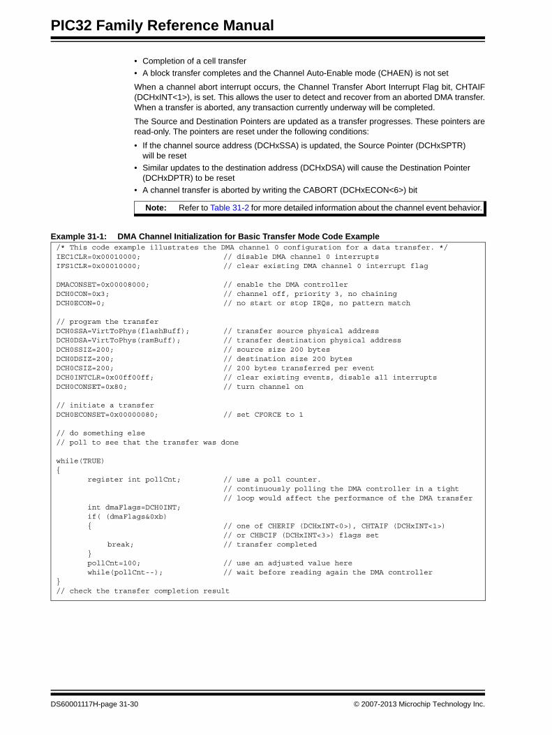
Example 31-1: DMA Channel Initialization for Basic Transfer Mode Code Example
Note: Refer to Table 31-2 for more detailed information about the channel event behavior.
/* This code example illustrates the DMA channel 0 configuration for a data transfer. */IEC1CLR=0x00010000; // disable DMA channel 0 interruptsIFS1CLR=0x00010000; // clear existing DMA channel 0 interrupt flag
DMACONSET=0x00008000; // enable the DMA controllerDCH0CON=0x3; // channel off, priority 3, no chainingDCH0ECON=0; // no start or stop IRQs, no pattern match
// program the transferDCH0SSA=VirtToPhys(flashBuff); // transfer source physical addressDCH0DSA=VirtToPhys(ramBuff); // transfer destination physical addressDCH0SSIZ=200; // source size 200 bytesDCH0DSIZ=200; // destination size 200 bytesDCH0CSIZ=200; // 200 bytes transferred per eventDCH0INTCLR=0x00ff00ff; // clear existing events, disable all interruptsDCH0CONSET=0x80; // turn channel on
// initiate a transferDCH0ECONSET=0x00000080; // set CFORCE to 1
// do something else// poll to see that the transfer was done
while(TRUE){
register int pollCnt; // use a poll counter.// continuously polling the DMA controller in a tight// loop would affect the performance of the DMA transfer
int dmaFlags=DCH0INT;if( (dmaFlags&0xb){ // one of CHERIF (DCHxINT<0>), CHTAIF (DCHxINT<1>)
// or CHBCIF (DCHxINT<3>) flags setbreak; // transfer completed
}pollCnt=100; // use an adjusted value herewhile(pollCnt--); // wait before reading again the DMA controller
}// check the transfer completion result
DS60001117H-page 31-30 © 2007-2013 Microchip Technology Inc.
Section 31. DMA ControllerD
MA
Co
ntro
ller
31
31.3.1.1 Interrupt and Pointer UpdatesThe Source and Destination Pointers are updated after every transaction. Interrupts will also beset or cleared at this time. If a pointer passes the halfway point during a transaction, theinterrupt will be updated accordingly.
Pointers are reset when any of the following occurs:
• On any device Reset• When the DMA is turned off (ON (DMACON<15>) bit is ‘0’)• A block transfer completes, regardless of the state of CHAEN (DCHxCON<4>) bit• A pattern match terminates a transfer, regardless of the state of CHAEN (DCHxCON<4>) bit• The CABORT (DCHxECON<6>) bit flag is written• Source or destination start addresses are updated
31.3.2 Pattern Match Termination Mode
Pattern Match Termination mode allows the user to end a transfer if data written during a trans-action matches a specific pattern, as defined by the DCHxDAT register. A pattern match istreated the same way as a block transfer complete, where the CHBCIF bit (DCHxINT<3>) is setand the CHEN bit (DCHxCON<7>) is cleared.
This feature is useful in applications where a variable data size is required and eases the setupof the DMA channel. The UART module is a good example of where this feature can beeffectively used.
Assuming a system has a series of messages that are routinely transmitted to an external hostand it has a maximum message size of 86 characters, the user would set the followingparameters on the channel:
• DCHxSSIZ to 87 bytes – If something unexpected occurs, the CPU program will be interrupted when the buffer overflows and can take the appropriate action
• DCHxDSIZ set to 1 byte• The destination address is set to the UART TXREG• The DCHxDAT is set to 0x00, which will stop the transfer on a NULL character in any byte
lane• The CHSIRQ<7:0> bits (DCHxECON<15:8>) are set to the UART “transmit buffer empty” IRQ• The SIRQEN bit (DCHxECON<4>) is set to enable the channel to respond to the start
interrupt event• The start address is set to the start address of the message to be transferred• The channel is enabled, CHEN (DCHxCON<7>) = 1
• The user will then force a cell transfer through CFORCE bit (DCHxECON<7>) and the first byte transmission by the UART
• Each time a byte is transmitted by the UART, the transmit buffer empty interrupt will initiate the following byte transfer from the source to the UART
• When the DMA channel detects a NULL character in any of the byte lanes of the channel, the transaction will be completed and the channel disabled
Pattern matching is independent of the byte lane of the source data. If ANY byte in the sourcebuffer matches DCHxDAT, a pattern match is detected. The transaction will be completed andthe data read from the source will be written to the destination.
31.3.2.1 PATTERN MATCH IGNORE MODE
In devices with a CHPATLEN bit, a pattern can either be 8 bits or 16 bits wide. This patternlength is defined by the CHPATLEN bit in the DCHxCON register. If the CHPATLEN bit is set toa ‘1’, the Pattern Match Ignore mode can be used. If the Enable Pattern Ignore Byte bit(CHPIGNEN) is set, and when the value in the Channel Register Data bits, CHPIGN<7:0>, ismet, the data being transferred is treated as a “don’t care” when trying to find a termination pat-tern during a cell transfer. An example of this condition is when there are space charactersfound between the end of a line and a carriage return. If an end of line is known as an ‘X’ and acarriage return is known as a ‘Y’ and the CHPIGN<7:0> bits are set to ‘_’, when ‘X_Y’ is trans-ferred during a DMA cell transfer, a pattern match termination would be detected since thezeroes in between would be ignored by the SFM when detecting a Pattern Match.
© 2007-2013 Microchip Technology Inc. DS60001117H-page 31-31
PIC32 Family Reference Manual
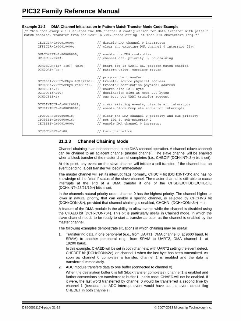
Example 31-2: DMA Channel Initialization in Pattern Match Transfer Mode Code Example
31.3.3 Channel Chaining Mode
Channel chaining is an enhancement to the DMA channel operation. A channel (slave channel)can be chained to an adjacent channel (master channel). The slave channel will be enabledwhen a block transfer of the master channel completes (i.e., CHBCIF (DCHxINT<3>) bit is set).
At this point, any event on the slave channel will initiate a cell transfer. If the channel has anevent pending, a cell transfer will begin immediately.
The master channel will set its interrupt flags normally, CHBCIF bit (DCHxINT<3>) and has noknowledge of the “chain” status of the slave channel. The master channel is still able to causeinterrupts at the end of a DMA transfer if one of the CHSDIE/CHDDIE/CHBCIE(DCHxINT<23/21/19>) bits is set.
In the channels natural priority order, channel 0 has the highest priority. The channel higher orlower in natural priority, that can enable a specific channel, is selected by CHCHNS bit(DCHxCON<8>), provided that channel chaining is enabled, CHCHN (DCHxCON<5>) = 1.
A feature of the DMA module is the ability to allow events while the channel is disabled usingthe CHAED bit (DCHxCON<6>). This bit is particularly useful in Chained mode, in which theslave channel needs to be ready to start a transfer as soon as the channel is enabled by themaster channel.
The following examples demonstrate situations in which chaining may be useful:
1. Transferring data in one peripheral (e.g., from UART1, DMA channel 0, at 9600 baud, toSRAM) to another peripheral (e.g., from SRAM to UART2, DMA channel 1, at19200 baud).
In this example, CHAED will be set in both channels; with UART2 setting the event detect,CHEDET bit (DCHxCON<2>), on channel 1 when the last byte has been transmitted. Assoon as channel 0 completes a transfer, channel 1 is enabled and the data istransferred immediately.
2. ADC module transfers data to one buffer (connected to channel 0).
When the destination buffer 0 is full (block transfer completes), channel 1 is enabled andfurther conversions are transferred to buffer 1. In this case, CHAED will not be enabled. Ifit were, the last word transferred by channel 0 would be transferred a second time bychannel 1 (because the ADC interrupt event would have set the event detect flagCHEDET in both channels).
/* This code example illustrates the DMA channel 0 configuration for data transfer with pattern match enabled. Transfer from the UART1 a <CR> ended string, at most 200 characters long */
IEC1CLR=0x00010000; // disable DMA channel 0 interruptsIFS1CLR=0x00010000; // clear any existing DMA channel 0 interrupt flag
DMACONSET=0x00008000; // enable the DMA controllerDCH0CON=0x03; // channel off, priority 3, no chaining
DCH0ECON=(27 <<8)| 0x30; // start irq is UART1 RX, pattern match enabledDCH0DAT=’\r’; // pattern value, carriage return
// program the transferDCH0SSA=VirtToPhys(&U1RXREG); // transfer source physical addressDCH0DSA=VirtToPhys(ramBuff); // transfer destination physical addressDCH0SSIZ=1; // source size is 1 byteDCH0DSIZ=200; // destination size at most 200 bytesDCH0CSIZ=1; // one byte per UART transfer request
DCH0INTCLR=0x00ff00ff; // clear existing events, disable all interruptsDCH0INTSET=0x00090000; // enable Block Complete and error interrupts
IPC9CLR=0x0000001f; // clear the DMA channel 0 priority and sub-priorityIPC9SET=0x00000016; // set IPL 5, sub-priority 2IEC1SET=0x00010000; // enable DMA channel 0 interrupt
DCH0CONSET=0x80; // turn channel on
DS60001117H-page 31-32 © 2007-2013 Microchip Technology Inc.

Section 31. DMA ControllerD
MA
Co
ntro
ller
31
Example 31-3: DMA Channel Initialization in Chaining Mode Code Example/* This code example illustrates the DMA channel 0 configuration for data transfer with pattern match enabled. DMA channel 0 transfer from the UART1 to a RAM buffer while DMA channel 1 transfers data from the RAM buffer to UART2. Transferred strings are at most 200 characters long. Transfer on UART2 starts as soon as the UART1 transfer is completed. */unsigned char myBuff<200>; // transfer buffer
IEC1CLR=0x00010000; // disable DMA channel 0 interruptsIFS1CLR=0x00010000; // clear any existing DMA channel 0 interrupt flag
DMACONSET=0x00008000; // enable the DMA controller
DCH0CON=0x3; // channel 0 off, priority 3, no chainingDCH1CON=0x62; // channel 1 off, priority 2
// chain to higher priority// (channel 0), enable events detection while disabled
DCH0ECON=(27 <<8)| 0x30; // start IRQ is UART1 RX, pattern enabledDCH1ECON=(42 <<8)| 0x30; // start IRQ is UART1 TX, pattern enabled
DCH0DAT=DCH1DAT=’\r’; // pattern value, carriage return
// program channel 0 transferDCH0SSA=VirtToPhys(&U1RXREG); // transfer source physical addressDCH0DSA=VirtToPhys(myBuff); // transfer destination physical addressDCH0SSIZ=1; // source size is 1 byteDCH0DSIZ=200; // dst size at most 200 bytesDCH0CSIZ=1; // one byte per UART transfer request
// program channel 1 transferDCH1SSA=VirtToPhys(myBuff); // transfer source physical addressDCH1DSA=VirtToPhys(&U2TXREG); // transfer destination physical addressDCH1SSIZ=200; // source size at most 200 bytesDCH1DSIZ=0; // dst size is 1 byteDCH1CSIZ=1; // one byte per UART transfer request
DCH0INTCLR=0x00ff00ff; // DMA0: clear events, disable interruptsDCH1INTCLR=0x00ff00ff; // DMA1: clear events, disable interruptsDCH1INTSET=0x00090000; // DMA1: enable Block Complete and error interrupts
IPC9CLR=0x00001f1f; // clear the DMA channels 0 and 1 priority and// sub-priority
IPC9SET=0x00000b16; // set IPL 5, sub-priority 2 for DMA channel 0// set IPL 2, sub-priority 3 for DMA channel 1
IEC1SET=0x00020000; // enable DMA channel 1 interrupt
DCH0CONSET=0x80; // turn channel on
© 2007-2013 Microchip Technology Inc. DS60001117H-page 31-33
PIC32 Family Reference Manual
31.3.4 Channel Auto-Enable Mode
The channel auto-enable can be used to keep a channel active, even if a block transfercompletes or pattern match occurs. This prevents the user from having to re-enable the channeleach time a block transfer completes. To use this mode the user will configure the channel,setting the CHAEN bit (DCHxCON<4>) before enabling the channel (i.e., setting the CHEN bit(DCHxCON<7>)). The channel will behave as normal except that normal termination of atransfer will not result in the channel being disabled.
Normal block transfer completion is defined as:
• Block transfer complete
• Pattern match detect
As before, the Channel Pointers will be reset. This mode is useful for applications that dorepeated pattern matching.
31.3.5 Special Function Module (SFM) Mode
The DMA module has one integrated Special Function Module (SFM) shared by all channels.
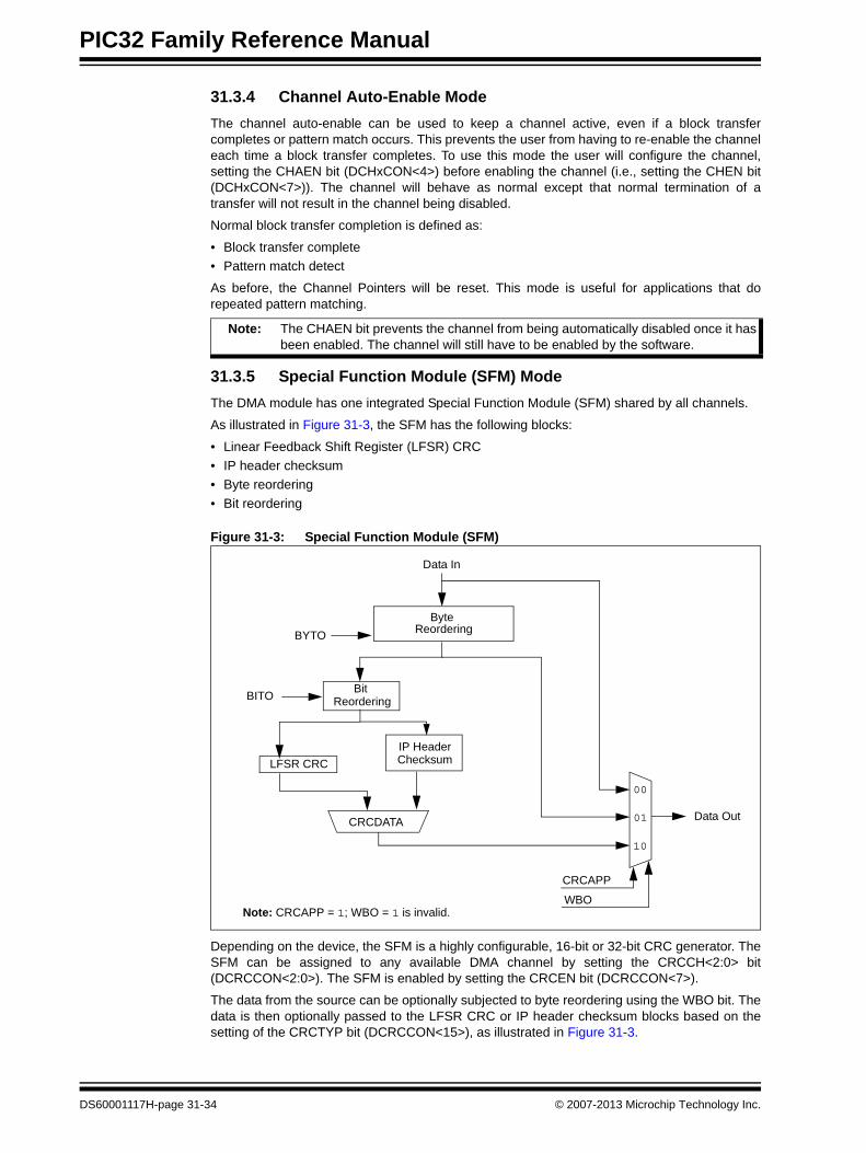
As illustrated in Figure 31-3, the SFM has the following blocks:
• Linear Feedback Shift Register (LFSR) CRC
• IP header checksum
• Byte reordering
• Bit reordering
Figure 31-3: Special Function Module (SFM)
Depending on the device, the SFM is a highly configurable, 16-bit or 32-bit CRC generator. TheSFM can be assigned to any available DMA channel by setting the CRCCH<2:0> bit(DCRCCON<2:0>). The SFM is enabled by setting the CRCEN bit (DCRCCON<7>).
The data from the source can be optionally subjected to byte reordering using the WBO bit. Thedata is then optionally passed to the LFSR CRC or IP header checksum blocks based on thesetting of the CRCTYP bit (DCRCCON<15>), as illustrated in Figure 31-3.
Note: The CHAEN bit prevents the channel from being automatically disabled once it hasbeen enabled. The channel will still have to be enabled by the software.
Data In
ByteReordering
LFSR CRC
BYTO
CRCDATA
CRCAPP
WBO
Data Out
Bit ReorderingBITO
Note: CRCAPP = 1; WBO = 1 is invalid.
00
01
10
IP HeaderChecksum
DS60001117H-page 31-34 © 2007-2013 Microchip Technology Inc.
Section 31. DMA ControllerD
MA
Co
ntro
ller
31
Further, the SFM modifies the behavior of the DMA channel associated with the SFM. Thebehavior of the channel is selected by the CRCAPP bit (DCRCCON<6>), resulting in thefollowing two modes:• Background mode: CRC is calculated in the background, with normal DMA behavior maintained (see 31.3.5.1 “CRC Background Mode (CRCAPP = 0)”).
• Append mode: Data read from the source is not written to the destination, but the CRC data is accumulated in the CRC data register. The accumulated CRC is written to the location given by the DCHxDSA register when a block transfer completes (see 31.3.5.2 “CRC Append Mode (CRCAPP = 1)”).
The order in which data is written to the destination can be selected using the WBO bit(DCRCCON<27>). If the WBO bit is cleared, the writes to the destination are unaltered. If theWBO bit is set, the writes to the destination are reordered as defined by the CRC Byte OrderSelection bits, BYTO<1:0> (DCRCCON<29:28>).
The SFM generator can be seeded by writing to the DCRCDATA register before enabling thechannel.
When in IP Header Checksum mode (CRCTYP (DCRCCON<15>) = 1), data written reads backas the 1’s complement form as this is the current value of the checksum.
The CRC value in DCRCDATA can be read at any time during the CRC generation, but is onlyvalid once the transfer completes.
31.3.5.1 CRC BACKGROUND MODE (CRCAPP = 0)
In this mode, the behavior of the DMA channel is maintained. The DMA reads the data from thesource, passes it through the CRC module and writes it to the destination. Writes to thedestination obey the WBO selection. In this mode, the calculated CRC is left in the DCRCDATAregister at the end of the block transfer.
This mode can be used to calculate a CRC as data is moved from a source address to adestination address. The data source can be either a memory buffer or a FIFO in a peripheral.Likewise, the destination can be either a memory buffer or a FIFO. When the data transfercompletes, the user can read the calculated CRC value and either append it to the transmitteddata or verify the received CRC data.
Background mode potentially ties up the CRC module for extended periods of time. For instance,when assigned to a UART data stream, the SFM cannot be used by another channel until theUART data stream completes.
Note: This feature is not available on all devices. Refer to the “Direct Memory Access(DMA) Controller” chapter in the specific device data sheet for availability.
Note 1: If a DMA Transfer is aborted while a CRC calculation is in progress, the DMA chan-nel should be reset before the next CRC calculation is started. Alternatively, thesame channel or another unused channel can be configured to transfer two or morebytes. The transfer should then be initiated and allowed to complete. The CRCmodule is then ready for the next CRC calculation.
2: If a DMA channel is disabled (CHEN (DCHxCON<7>) = 0) when a CRC calculationis in progress, the value in the DCRCDATA register is not updated. The same chan-nel or another unused channel can be configured to transfer two or more bytes. Thetransfer should then be initiated and allowed to complete. When the transfer is com-plete, the DCRCDATA value will be correct for the number of byte processed priorto the stop being issued. The DMA address register can be inspected to determinethe address range of the current CRC value.
© 2007-2013 Microchip Technology Inc. DS60001117H-page 31-35
PIC32 Family Reference Manual
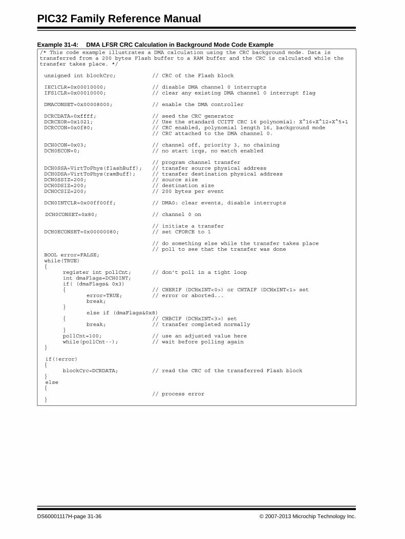
Example 31-4: DMA LFSR CRC Calculation in Background Mode Code Example/* This code example illustrates a DMA calculation using the CRC background mode. Data is transferred from a 200 bytes Flash buffer to a RAM buffer and the CRC is calculated while the transfer takes place. */
unsigned int blockCrc; // CRC of the Flash block
IEC1CLR=0x00010000; // disable DMA channel 0 interruptsIFS1CLR=0x00010000; // clear any existing DMA channel 0 interrupt flag
DMACONSET=0x00008000; // enable the DMA controller
DCRCDATA=0xffff; // seed the CRC generatorDCRCXOR=0x1021; // Use the standard CCITT CRC 16 polynomial: X^16+X^12+X^5+1DCRCCON=0x0f80; // CRC enabled, polynomial length 16, background mode
// CRC attached to the DMA channel 0.
DCH0CON=0x03; // channel off, priority 3, no chainingDCH0ECON=0; // no start irqs, no match enabled
// program channel transferDCH0SSA=VirtToPhys(flashBuff); // transfer source physical addressDCH0DSA=VirtToPhys(ramBuff); // transfer destination physical addressDCH0SSIZ=200; // source sizeDCH0DSIZ=200; // destination sizeDCHOCSIZ=200; // 200 bytes per event
DCH0INTCLR=0x00ff00ff; // DMA0: clear events, disable interrupts
DCH0CONSET=0x80; // channel 0 on
// initiate a transferDCH0ECONSET=0x00000080; // set CFORCE to 1
// do something else while the transfer takes place// poll to see that the transfer was done
BOOL error=FALSE;while(TRUE){
register int pollCnt; // don’t poll in a tight loopint dmaFlags=DCH0INT;if( (dmaFlags& 0x3){ // CHERIF (DCHxINT<0>) or CHTAIF (DCHxINT<1> set
error=TRUE; // error or aborted...break;
}else if (dmaFlags&0x8)
{ // CHBCIF (DCHxINT<3>) setbreak; // transfer completed normally
}pollCnt=100; // use an adjusted value herewhile(pollCnt--); // wait before polling again
}
if(!error){
blockCrc=DCRDATA; // read the CRC of the transferred Flash block}else{
// process error}
DS60001117H-page 31-36 © 2007-2013 Microchip Technology Inc.
Section 31. DMA ControllerD
MA
Co
ntro
ller
31
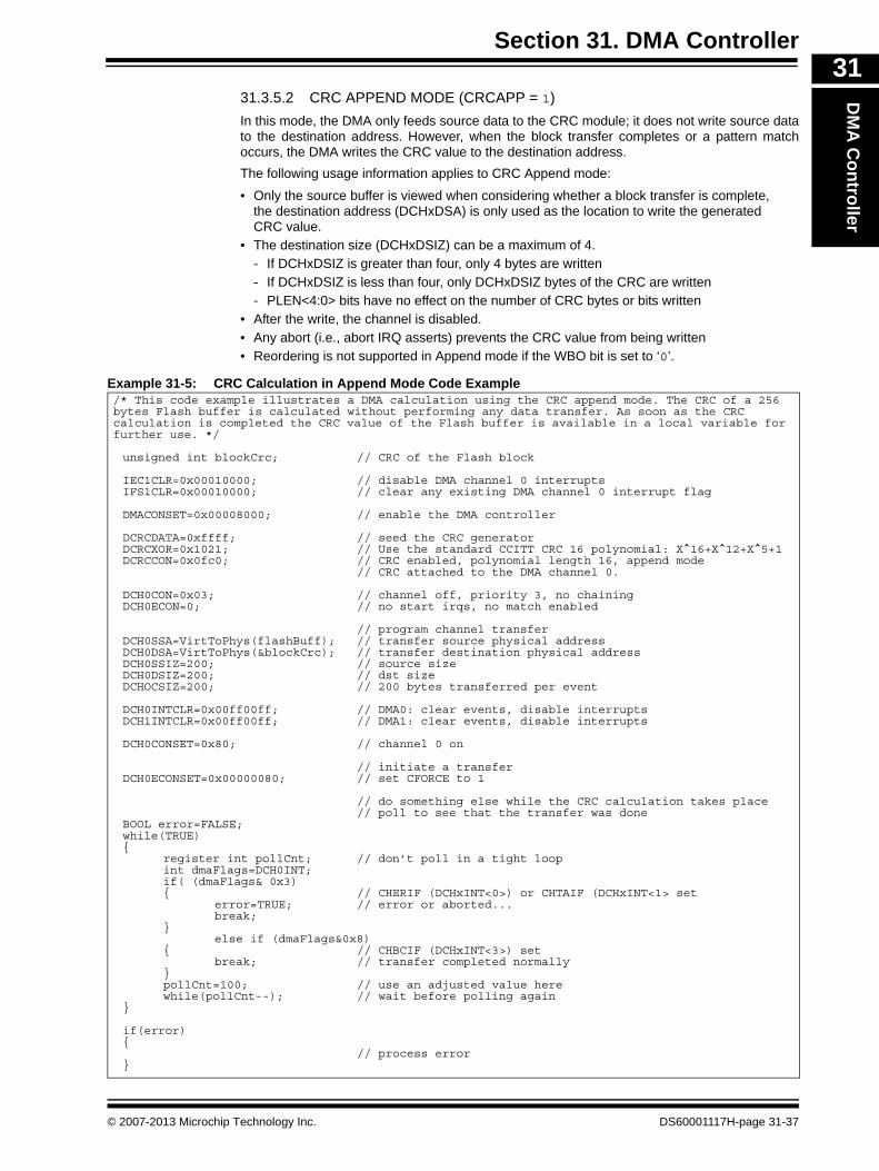
31.3.5.2 CRC APPEND MODE (CRCAPP = 1)In this mode, the DMA only feeds source data to the CRC module; it does not write source datato the destination address. However, when the block transfer completes or a pattern matchoccurs, the DMA writes the CRC value to the destination address.
The following usage information applies to CRC Append mode:
• Only the source buffer is viewed when considering whether a block transfer is complete, the destination address (DCHxDSA) is only used as the location to write the generated CRC value.
• The destination size (DCHxDSIZ) can be a maximum of 4. - If DCHxDSIZ is greater than four, only 4 bytes are written- If DCHxDSIZ is less than four, only DCHxDSIZ bytes of the CRC are written- PLEN<4:0> bits have no effect on the number of CRC bytes or bits written
• After the write, the channel is disabled.• Any abort (i.e., abort IRQ asserts) prevents the CRC value from being written• Reordering is not supported in Append mode if the WBO bit is set to ‘0’.
Example 31-5: CRC Calculation in Append Mode Code Example/* This code example illustrates a DMA calculation using the CRC append mode. The CRC of a 256 bytes Flash buffer is calculated without performing any data transfer. As soon as the CRC calculation is completed the CRC value of the Flash buffer is available in a local variable for further use. */
unsigned int blockCrc; // CRC of the Flash block
IEC1CLR=0x00010000; // disable DMA channel 0 interruptsIFS1CLR=0x00010000; // clear any existing DMA channel 0 interrupt flag
DMACONSET=0x00008000; // enable the DMA controller
DCRCDATA=0xffff; // seed the CRC generatorDCRCXOR=0x1021; // Use the standard CCITT CRC 16 polynomial: X^16+X^12+X^5+1 DCRCCON=0x0fc0; // CRC enabled, polynomial length 16, append mode
// CRC attached to the DMA channel 0.
DCH0CON=0x03; // channel off, priority 3, no chainingDCH0ECON=0; // no start irqs, no match enabled
// program channel transferDCH0SSA=VirtToPhys(flashBuff); // transfer source physical addressDCH0DSA=VirtToPhys(&blockCrc); // transfer destination physical addressDCH0SSIZ=200; // source size DCH0DSIZ=200; // dst size DCHOCSIZ=200; // 200 bytes transferred per event
DCH0INTCLR=0x00ff00ff; // DMA0: clear events, disable interruptsDCH1INTCLR=0x00ff00ff; // DMA1: clear events, disable interrupts
DCH0CONSET=0x80; // channel 0 on
// initiate a transferDCH0ECONSET=0x00000080; // set CFORCE to 1
// do something else while the CRC calculation takes place// poll to see that the transfer was done
BOOL error=FALSE;while(TRUE){
register int pollCnt; // don’t poll in a tight loopint dmaFlags=DCH0INT;if( (dmaFlags& 0x3){ // CHERIF (DCHxINT<0>) or CHTAIF (DCHxINT<1> set
error=TRUE; // error or aborted...break;
}else if (dmaFlags&0x8)
{ // CHBCIF (DCHxINT<3>) setbreak; // transfer completed normally
}pollCnt=100; // use an adjusted value herewhile(pollCnt--); // wait before polling again
}
if(error){
// process error}
© 2007-2013 Microchip Technology Inc. DS60001117H-page 31-37
PIC32 Family Reference Manual
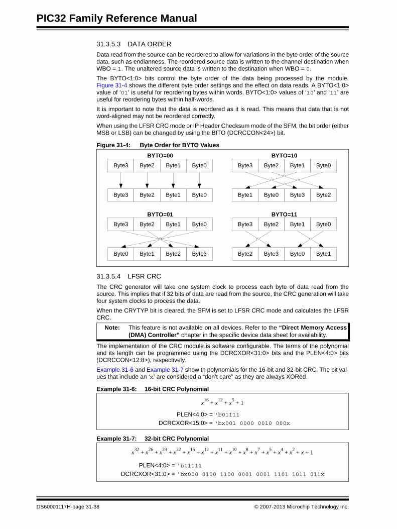
31.3.5.3 DATA ORDER
Data read from the source can be reordered to allow for variations in the byte order of the sourcedata, such as endianness. The reordered source data is written to the channel destination whenWBO = 1. The unaltered source data is written to the destination when WBO = 0.
The BYTO<1:0> bits control the byte order of the data being processed by the module.Figure 31-4 shows the different byte order settings and the effect on data reads. A BYTO<1:0>value of ‘01’ is useful for reordering bytes within words. BYTO<1:0> values of ‘10’ and ‘11’ areuseful for reordering bytes within half-words.
It is important to note that the data is reordered as it is read. This means that data that is notword-aligned may not be reordered correctly.
When using the LFSR CRC mode or IP Header Checksum mode of the SFM, the bit order (eitherMSB or LSB) can be changed by using the BITO (DCRCCON<24>) bit.
Figure 31-4: Byte Order for BYTO Values
31.3.5.4 LFSR CRC
The CRC generator will take one system clock to process each byte of data read from thesource. This implies that if 32 bits of data are read from the source, the CRC generation will takefour system clocks to process the data.
When the CRYTYP bit is cleared, the SFM is set to LFSR CRC mode and calculates the LFSRCRC.
The implementation of the CRC module is software configurable. The terms of the polynomialand its length can be programmed using the DCRCXOR<31:0> bits and the PLEN<4:0> bits(DCRCCON<12:8>), respectively.
Example 31-6 and Example 31-7 show th polynomials for the 16-bit and 32-bit CRC. The bit val-ues that include an ‘x’ are considered a “don’t care” as they are always XORed.
Example 31-6: 16-bit CRC Polynomial
Example 31-7: 32-bit CRC Polynomial
Note: This feature is not available on all devices. Refer to the “Direct Memory Access(DMA) Controller” chapter in the specific device data sheet for availability.
Byte3 Byte2 Byte1 Byte0
Byte3 Byte2 Byte1 Byte0
Byte3 Byte2 Byte1 Byte0
Byte3Byte2Byte1Byte0
Byte3 Byte2 Byte1 Byte0
Byte3 Byte2Byte1 Byte0
Byte3 Byte2 Byte1 Byte0
Byte3Byte2 Byte1Byte0
BYTO=00
BYTO=01 BYTO=11
BYTO=10
x16 x12 x5 1+ + +
PLEN<4:0> = ‘b01111
DCRCXOR<15:0> = ‘bx001 0000 0010 000x
x32 x26 x23 x22 x16 x12 x11 x10 x8 x7 x5 x4 x2 x 1+ + + + + + + + + + + + + +
PLEN<4:0> = ‘b11111
DCRCXOR<31:0> = ‘bx000 0100 1100 0001 0001 1101 1011 011x
DS60001117H-page 31-38 © 2007-2013 Microchip Technology Inc.
Section 31. DMA ControllerD
MA
Co
ntro
ller
31
The PLEN<4:0> bits (DCRCCON<12:8>) in the CRC generator are used to select which bit isused as the feedback point of the CRC. For a 16-bit CRC example, if PLEN<4:0> = 00110, bit 6of the Shift register is fed into the XOR gates of all bits set in the CRCXOR register.The CRCXOR feedback points are specified using the DCRCXOR register. Setting the Nth bit inthe DCRCXOR register will enable the input to the Nth bit of the CRC Shift register to be XORedwith the (PLEN + 1)th bit of the CRC Shift register. Bit 0 and bit 15 of the CRC generator isalways XORed.
31.3.5.5 CALCULATING THE IP HEADER CHECKSUM
When the CRCTYP bit (DCRCCON<15>) bit is set, the SFM calculates the IP header checksum.Use the following procedure to calculate the IP header checksum:
1. Configure a channel to point to the IP header.
2. Configure CRCCON to enable the SFM and select the channel being used.
3. Set the CRCTYP bit, which selects IP Header checksum.
4. Set DCRCDATA to ‘0000’.
5. Start the transfer.
6. When the transfer completes, read the data out of the DCRCDATA register.
Note: This feature is not available on all devices. Refer to the “Direct Memory Access(DMA) Controller” chapter in the specific device data sheet for availability.
© 2007-2013 Microchip Technology Inc. DS60001117H-page 31-39
PIC32 Family Reference Manual
31.4 CHANNEL CONTROL
31.4.1 Channel Enable
Each channel has an enable bit, CHEN (DCHxCON<7>), which can be used to enable ordisable the channel in question. When this bit is set, the channel transfer requests are servicedby the DMA controller.
When the CHEN bit is clear, the state of the channel is preserved (this allows the channel to besuspended once a transfer has begun).
The CHEN bit will be cleared by hardware under the following conditions:
• A block transfer is complete, the pointer to the larger of the source or destination matches the size (only if the CHAEN (DCHxCON<4>) bit is clear)
• A pattern match occurs in Pattern Match mode (only if the CHAEN bit is clear)• An abort interrupt occurs• The user writes the CABORT (DCHxECON<6>) bit
31.4.2 Channel Transfer Behavior
Once a channel has been enabled, CHEN = 1, any event that starts a cell transfer will transferthe CHCSIZ<15:0> (DCHxCSIZ<15:0>) bytes of data. This will require one or moretransactions. Once the cell transfer is complete the channel will return to an inactive state, andwill wait for another channel start event to occur before starting another cell transfer.
When the larger of CHSSIZ<15:0> (DCHxSSIZ<15:0>) or CHDSIZ<15:0> (DCHxDSIZ<15:0>)bytes are transferred, a block transfer completes, the channel transfer will be halted and thechannel will be disabled (i.e., CHEN set to ‘0’ by hardware, and pointers are reset).
31.4.2.1 CHANNEL EVENT TRANSFER INITIATION
A given channel transfer can be initiated by:
• Writing the CFORCE bit (DCHxECON<7>)• An interrupt occurs that matches the value of CHSIRQ<7:0> (DCHxECON<15:8>) if it is
enabled by SIRQEN bit (DCHxECON<4>)
Channel events are registered if the channel is enabled (CHEN = 1), or if “Allow Event IfDisabled” is set (i.e., CHAED (DCHxCON<6>) = 1)
31.4.2.2 CHANNEL EVENT TRANSFER TERMINATION
Channel transfer is terminated in any of the following cases:
• A transfer is aborted as described in 31.4.6 “Resetting the Channel”• A cell transfer (CHCSIZ<15:0> bytes (DCHxCSIZ<15:0> transferred)) completes• The DMA has transferred the larger of CHSSIZ<15:0> or CHDSIZ<15:0> bytes (block
transfer complete), the channel is disabled in hardware and must be re-enabled by user software before the channel will respond to channel events
• A pattern match occurs if enabled• An abort interrupt, CHAIRQ<7:0> (DCHxECON<23:16>), occurs if abort interrupts are
enabled by AIRQEN bit (DCHxECON<3>)• An address error occurs
An example of how to use the abort interrupt would be a transfer from a UART channel to thememory. While the UART Receive Data Available interrupt can be used to start the transfer, theUART Error interrupt can abort the transfer. This way, whenever an error occurs on the commu-nication channel (a framing/parity error or even an overrun), the transfer is stopped and the usercode gets control in an ISR (if the abort interrupt is enabled for the DMA controller).
A summary of the status flags affected by channel transfer initiation or termination is provided inTable 31-2. Channel abort events are allowed if the channel is enabled, CHEN = 1, or if the userelects to allow events while the channel is disabled, CHAED = 1.
DS60001117H-page 31-40 © 2007-2013 Microchip Technology Inc.
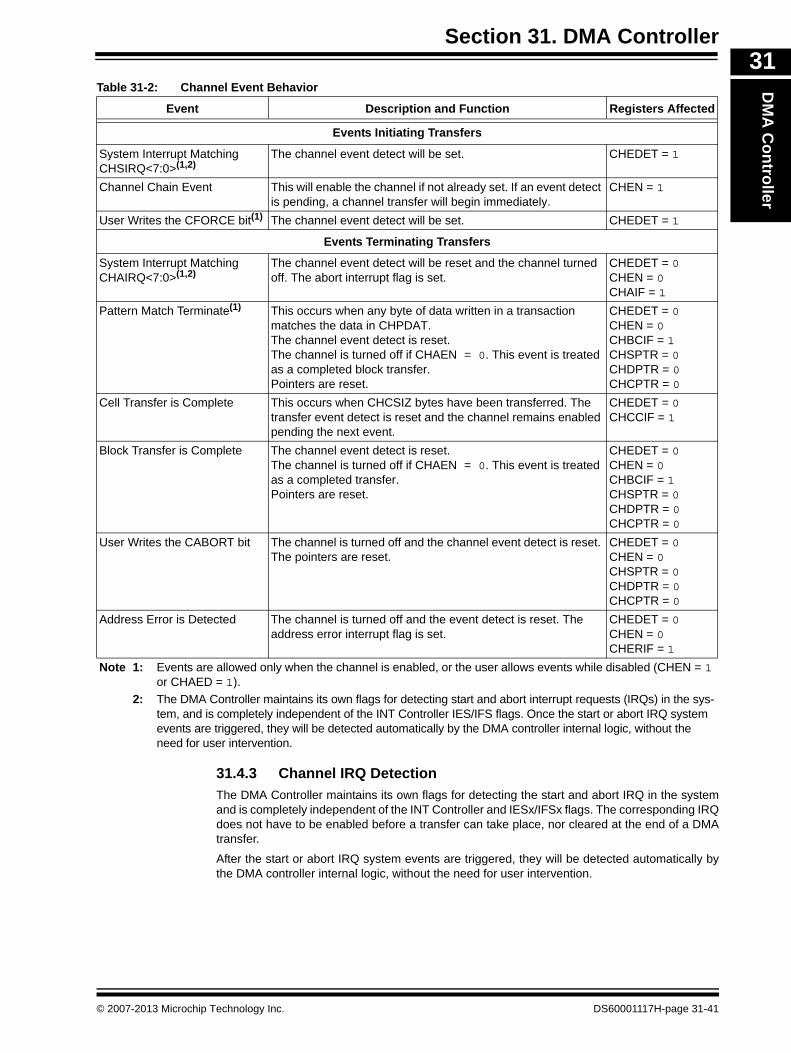
Section 31. DMA ControllerD
MA
Co
ntro
ller
31
Table 31-2: Channel Event Behavior31.4.3 Channel IRQ Detection
The DMA Controller maintains its own flags for detecting the start and abort IRQ in the systemand is completely independent of the INT Controller and IESx/IFSx flags. The corresponding IRQdoes not have to be enabled before a transfer can take place, nor cleared at the end of a DMAtransfer.
After the start or abort IRQ system events are triggered, they will be detected automatically bythe DMA controller internal logic, without the need for user intervention.
Event Description and Function Registers Affected
Events Initiating Transfers
System Interrupt Matching CHSIRQ<7:0>(1,2)
The channel event detect will be set. CHEDET = 1
Channel Chain Event This will enable the channel if not already set. If an event detect is pending, a channel transfer will begin immediately.
CHEN = 1
User Writes the CFORCE bit(1) The channel event detect will be set. CHEDET = 1
Events Terminating Transfers
System Interrupt Matching CHAIRQ<7:0>(1,2)
The channel event detect will be reset and the channel turned off. The abort interrupt flag is set.
CHEDET = 0CHEN = 0CHAIF = 1
Pattern Match Terminate(1) This occurs when any byte of data written in a transaction matches the data in CHPDAT.The channel event detect is reset.The channel is turned off if CHAEN = 0. This event is treated as a completed block transfer.Pointers are reset.
CHEDET = 0CHEN = 0CHBCIF = 1CHSPTR = 0CHDPTR = 0CHCPTR = 0
Cell Transfer is Complete This occurs when CHCSIZ bytes have been transferred. The transfer event detect is reset and the channel remains enabled pending the next event.
CHEDET = 0CHCCIF = 1
Block Transfer is Complete The channel event detect is reset.The channel is turned off if CHAEN = 0. This event is treated as a completed transfer.Pointers are reset.
CHEDET = 0CHEN = 0CHBCIF = 1CHSPTR = 0CHDPTR = 0CHCPTR = 0
User Writes the CABORT bit The channel is turned off and the channel event detect is reset. The pointers are reset.
CHEDET = 0CHEN = 0CHSPTR = 0CHDPTR = 0CHCPTR = 0
Address Error is Detected The channel is turned off and the event detect is reset. The address error interrupt flag is set.
CHEDET = 0CHEN = 0CHERIF = 1
Note 1: Events are allowed only when the channel is enabled, or the user allows events while disabled (CHEN = 1 or CHAED = 1).
2: The DMA Controller maintains its own flags for detecting start and abort interrupt requests (IRQs) in the sys-tem, and is completely independent of the INT Controller IES/IFS flags. Once the start or abort IRQ system events are triggered, they will be detected automatically by the DMA controller internal logic, without the need for user intervention.
© 2007-2013 Microchip Technology Inc. DS60001117H-page 31-41
PIC32 Family Reference Manual
31.4.4 Channel Abort Interrupt
A channel can elect to abort a cell transfer if an interrupt event occurs. The interrupt is selectedby the channel’s abort IRQ, CHAIRQ<7:0> (DCHxECON<23:16>). Any one of the deviceinterrupt events can cause a channel abort. An abort only occurs if enabled by the AIRQEN bit(DCHxECON<3>).
If this occurs (often a timer time-out or a module error flag), the channel’s status flags willindicate the external abort event on the channel in question by setting its CHTAIF bit(DCHxINT<1>).The Source and Destination Pointers are not reset, allowing the user to recoverfrom the error.
31.4.5 DMA Suspend
DMA transactions are suspended immediately if the SUSPEND bit (DMACON<12>) is set. Thecurrent read or write will be completed. If the suspend comes during the read portion of thetransaction, the transaction will be suspended and the write will be put on hold. If the suspendcomes during the write portion of the transaction, the write will complete and the pointersupdated as normal. Any transactions that were in process will continue where they left off whenthe SUSPEND bit is cleared.
Depending on the device, when the DMA module is suspended by setting the SUSPEND bit,the user application should poll the DMABUSY bit (DMACON<11>) to determine when themodule is completely suspended following the completion of the current transaction.
Example 31-8: DMA Controller Suspension
Individual channels may be suspended using the CHEN bit (DCHxCON<7>). If a DMA transferis in progress and the CHEN bit is cleared, the current transaction will be completed and furthertransactions on the channel will be suspended.
Depending on the device, when the channel is suspended by clearing the CHEN bit, the userapplication should poll the CHBUSY bit (DCHxCON<15>) to determine when the channel iscompletely suspended following completion of the current transaction.
Clearing the enable bit, CHEN, will not affect the Channel Pointers or the transaction counters.While a channel is suspended, the user can elect to continue to receive events (abort interrupts,etc.) by setting the CHAED bit (DCHxCON<6>).
31.4.6 Resetting the Channel
The channel logic will be reset on any device Reset. The channel is also reset when the channelbit, CABORT (DCHxECON<6>), is set. This will turn off the channel bit, CHEN = 0, clear theSource and Destination Pointers, and reset the event detector. When the CABORT bit is set, thecurrent transaction in progress (if any) will complete before the channel is reset, but any remainingtransactions will be aborted.
The user should modify the channel registers only while the channel is disabled (CHEN = 0).Modifying the Source and Destination registers will reset the corresponding pointer registers(DCHxSPTR or DCHxDPTR).
Note: The DMABUSY bit is not available on all device. Refer to the “Direct MemoryAccess (DMA) Controller” chapter in the specific device data sheet for availability.
Note: The channel size must be changed while the channel is disabled.
/* This code example will suspend the DMA Controller. */
DMACONSET=0x00001000; // suspend the DMA controller
while(!(DMACONbits.busy)); // wait for the transfer to be suspended
// let the CPU have complete control of the bus
DMACONCLR=0x00001000; // clear the suspend mode and let the DMA// operate normally. From now on, the CPU and// DMA controller share the bus access
DS60001117H-page 31-42 © 2007-2013 Microchip Technology Inc.
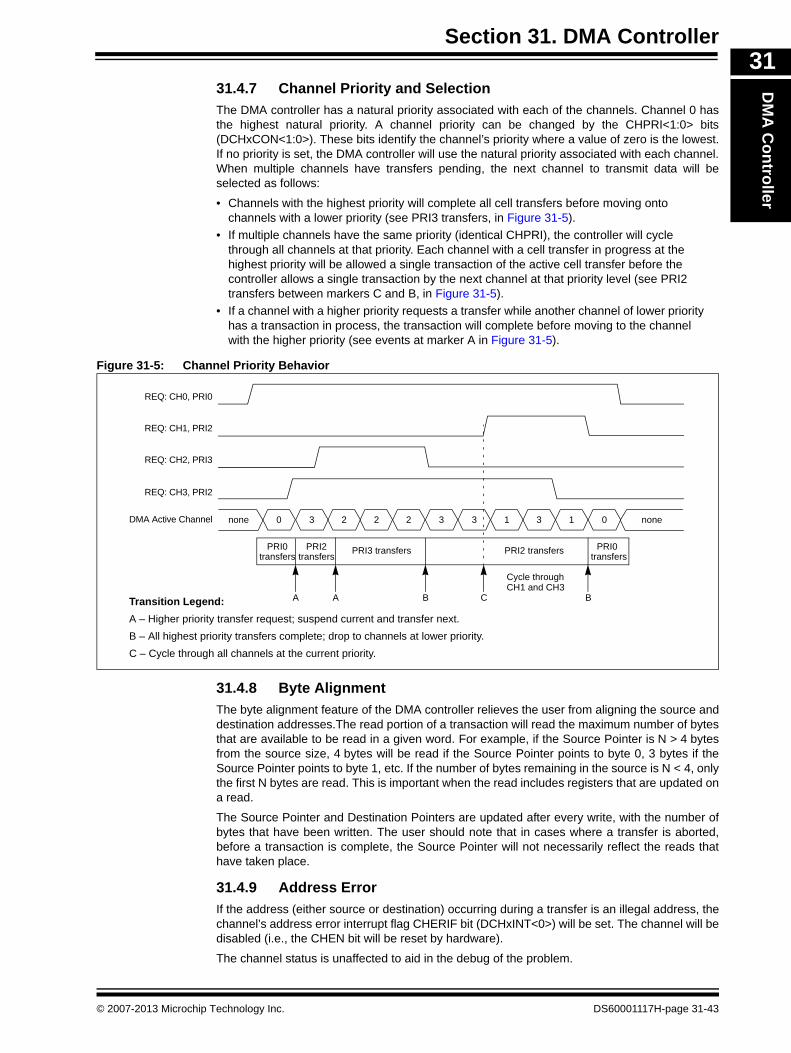
Section 31. DMA ControllerD
MA
Co
ntro
ller
31
31.4.7 Channel Priority and SelectionThe DMA controller has a natural priority associated with each of the channels. Channel 0 hasthe highest natural priority. A channel priority can be changed by the CHPRI<1:0> bits(DCHxCON<1:0>). These bits identify the channel’s priority where a value of zero is the lowest.If no priority is set, the DMA controller will use the natural priority associated with each channel.When multiple channels have transfers pending, the next channel to transmit data will beselected as follows:
• Channels with the highest priority will complete all cell transfers before moving onto channels with a lower priority (see PRI3 transfers, in Figure 31-5).
• If multiple channels have the same priority (identical CHPRI), the controller will cycle through all channels at that priority. Each channel with a cell transfer in progress at the highest priority will be allowed a single transaction of the active cell transfer before the controller allows a single transaction by the next channel at that priority level (see PRI2 transfers between markers C and B, in Figure 31-5).
• If a channel with a higher priority requests a transfer while another channel of lower priority has a transaction in process, the transaction will complete before moving to the channel with the higher priority (see events at marker A in Figure 31-5).
Figure 31-5: Channel Priority Behavior
31.4.8 Byte Alignment
The byte alignment feature of the DMA controller relieves the user from aligning the source anddestination addresses.The read portion of a transaction will read the maximum number of bytesthat are available to be read in a given word. For example, if the Source Pointer is N > 4 bytesfrom the source size, 4 bytes will be read if the Source Pointer points to byte 0, 3 bytes if theSource Pointer points to byte 1, etc. If the number of bytes remaining in the source is N < 4, onlythe first N bytes are read. This is important when the read includes registers that are updated ona read.
The Source Pointer and Destination Pointers are updated after every write, with the number ofbytes that have been written. The user should note that in cases where a transfer is aborted,before a transaction is complete, the Source Pointer will not necessarily reflect the reads thathave taken place.
31.4.9 Address Error
If the address (either source or destination) occurring during a transfer is an illegal address, thechannel’s address error interrupt flag CHERIF bit (DCHxINT<0>) will be set. The channel will bedisabled (i.e., the CHEN bit will be reset by hardware).
The channel status is unaffected to aid in the debug of the problem.
REQ: CH0, PRI0
REQ: CH1, PRI2
REQ: CH2, PRI3
REQ: CH3, PRI2
DMA Active Channel none 0 3 2 2 2 3 3 31 1 0 none
PRI0transfers
PRI2transfers
PRI0transfers
PRI3 transfers PRI2 transfers
Cycle throughCH1 and CH3
A A B C BTransition Legend:
A – Higher priority transfer request; suspend current and transfer next.
B – All highest priority transfers complete; drop to channels at lower priority.
C – Cycle through all channels at the current priority.
© 2007-2013 Microchip Technology Inc. DS60001117H-page 31-43
PIC32 Family Reference Manual
31.5 INTERRUPTS
The DMA device has the ability to generate interrupts reflecting the events that occur during thechannel’s data transfer:
• Error interrupts, signaled by each channel’s CHERIF bit (DCHxINT<0>) and enabled using the CHERIE bit (DCHxINT<16>). This event occurs when there is an address error occurred during the channel transfer operation.
• Abort interrupts, signaled by each channel’s CHTAIF bit (DCHxINT<1>) and enabled using the CHTAIE bit (DCHxINT<17>). This event occurs when a DMA channel transfer gets aborted because of a system event (interrupt) matching the CHAIRQ<7:0> bits (DCHxECON<23:16>) when the abort interrupt request is enabled, AIRQEN (DCHxECON<3>) = 1.
• Block complete interrupts, signaled by each channel’s CHBCIF bit (DCHxINT<3>) and enabled using the CHBCIE bit (DCHxINT<19>). This event occurs when a DMA channel block transfer is completed.
• Cell complete interrupts, signaled by each channel’s CHCCIF bit (DCHxINT<2>) and enabled using the CHCCIE bit (DCHxINT<18>). This event occurs when a DMA channel cell transfer is completed.
• Source Address Pointer activity interrupts: either when the Channel Source Pointer reached the end of the source, signaled by the CHSDIF bit (DCHxINT<7>) and enabled by CHSDIE bit (DCHxINT<23>), or when the Channel Source Pointer reached midpoint of the source, signaled by the CHSHIF bit (DCHxINT<6>) and enabled by the CHSHIE bit (DCHxINT<22>).
• Destination Address Pointer activity interrupts: either when the Channel Destination Pointer reached the end of the destination, signaled by the CHDDIF bit (DCHxINT<5>) and enabled by the CHDDIE bit (DCHxINT<21>), or when the Channel Destination Pointer reached midpoint of the destination, signaled by the CHDHIF bit (DCHxINT<4>) and enabled by the CHDHIE bit (DCHxINT<20>).
All the interrupts belonging to a DMA channel map to the corresponding channel interrupt vector.
31.5.1 Interrupt Configuration
Each DMA channel internally has multiple interrupt flags (CHSDIF, CHSHIF, CHDDIF, CHDHIF,CHBCIF, CHCCIF, CHTAIF, CHERIF) and corresponding enable interrupt control bits (CHSDIE,CHSHIE, CHDDIE, CHDHIE, CHBCIE, CHCCIE, CHTAIE, CHERIE).
However, for the interrupt controller, there is just one dedicated interrupt flag bit per channel,DMAxIF, and the corresponding interrupt enable/mask bits, DMAxIE.
Therefore, note that all of the interrupt conditions for a specific DMA channel share just oneinterrupt vector. Each DMA channel can have its own priority level independent of other DMAchannels.
Note: Not all DMA channels are available on all devices. Refer to the “Interrupts” chapterin the specific device data sheet for availability.
Note: Depending on the device, up to eight (i.e., 0 through 7) interrupt flags and interruptenable/mask bits are available. Refer to the “Interrupts” chapter in the specificdevice data sheet for availability.
DS60001117H-page 31-44 © 2007-2013 Microchip Technology Inc.
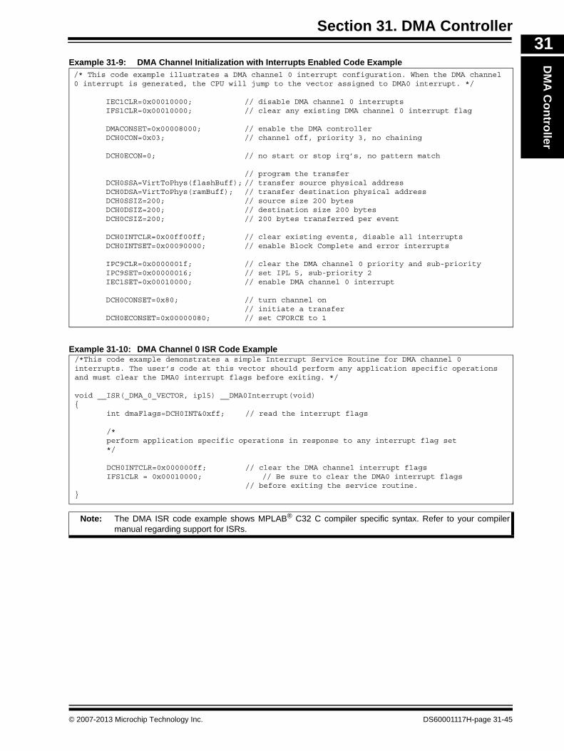
Section 31. DMA ControllerD
MA
Co
ntro
ller
31
Example 31-9: DMA Channel Initialization with Interrupts Enabled Code ExampleExample 31-10: DMA Channel 0 ISR Code Example
/* This code example illustrates a DMA channel 0 interrupt configuration. When the DMA channel 0 interrupt is generated, the CPU will jump to the vector assigned to DMA0 interrupt. */
IEC1CLR=0x00010000; // disable DMA channel 0 interruptsIFS1CLR=0x00010000; // clear any existing DMA channel 0 interrupt flag
DMACONSET=0x00008000; // enable the DMA controllerDCH0CON=0x03; // channel off, priority 3, no chaining
DCH0ECON=0; // no start or stop irq’s, no pattern match
// program the transferDCH0SSA=VirtToPhys(flashBuff); // transfer source physical addressDCH0DSA=VirtToPhys(ramBuff); // transfer destination physical addressDCH0SSIZ=200; // source size 200 bytesDCH0DSIZ=200; // destination size 200 bytesDCH0CSIZ=200; // 200 bytes transferred per event
DCH0INTCLR=0x00ff00ff; // clear existing events, disable all interruptsDCH0INTSET=0x00090000; // enable Block Complete and error interrupts
IPC9CLR=0x0000001f; // clear the DMA channel 0 priority and sub-priorityIPC9SET=0x00000016; // set IPL 5, sub-priority 2IEC1SET=0x00010000; // enable DMA channel 0 interrupt
DCH0CONSET=0x80; // turn channel on// initiate a transfer
DCH0ECONSET=0x00000080; // set CFORCE to 1
/*This code example demonstrates a simple Interrupt Service Routine for DMA channel 0 interrupts. The user’s code at this vector should perform any application specific operations and must clear the DMA0 interrupt flags before exiting. */
void __ISR(_DMA_0_VECTOR, ipl5) __DMA0Interrupt(void){
int dmaFlags=DCH0INT&0xff; // read the interrupt flags
/* perform application specific operations in response to any interrupt flag set */
DCH0INTCLR=0x000000ff; // clear the DMA channel interrupt flagsIFS1CLR = 0x00010000; // Be sure to clear the DMA0 interrupt flags
// before exiting the service routine.}
Note: The DMA ISR code example shows MPLAB® C32 C compiler specific syntax. Refer to your compilermanual regarding support for ISRs.
© 2007-2013 Microchip Technology Inc. DS60001117H-page 31-45
PIC32 Family Reference Manual
31.6 OPERATION IN POWER-SAVING AND DEBUG MODES
31.6.1 DMA Operation in Sleep Mode
When the device enters Sleep mode, the system clock is disabled. No DMA activity can occur inthis mode.
31.7 EFFECTS OF VARIOUS RESETS
31.7.1 Device Reset
All DMA registers are forced to their reset states upon a device Reset. When the asynchronousReset input goes active, the DMA logic:
• Resets all fields in DMACON, DMASTAT, DMAADDR, DCRCCON, DCRCDATA and DCRCXOR
• Sets the appropriate values in each channel’s register fields: DCHxCON, DCHxECON, DCHxINT, DCHxSSIZ, DCHxDSIZ, DCHxSPTR, DCHxDPTR, DCHxCSIZ, DCHxCPTR and DCHxDAT
• Registers DCHxSSA and DCHxDSA have random values after a reset
• Aborts any ongoing data transfers
31.7.2 Power-on Reset
All DMA registers are forced to their reset states upon a Power-on Reset.
31.7.3 Watchdog Timer Reset
All DMA registers are forced to their reset states upon a Watchdog Timer Reset.
DS60001117H-page 31-46 © 2007-2013 Microchip Technology Inc.
Section 31. DMA ControllerD
MA
Co
ntro
ller
31
31.8 RELATED APPLICATION NOTESThis section lists application notes that are related to this section of the manual. Theseapplication notes may not be written specifically for the PIC32 device family, but the concepts arepertinent and could be used DMA Controller with modification and possible limitations. Thecurrent application notes related to the Direct Memory Access (DMA) module are:
Title Application Note #
No related application notes at this time N/A
Note: Visit the Microchip web site (www.microchip.com) for additional application notesand code examples for the PIC32 family of devices.
© 2007-2013 Microchip Technology Inc. DS60001117H-page 31-47

PIC32 Family Reference Manual
31.9 REVISION HISTORY
Revision A (October 2007)
This is the initial released version of the document.
Revision B (October 2007)
Updated document to remove Confidential status.
Revision C (April 2008)
Revised status to Preliminary; Revised U-0 to r-x; Revised Table 31-1; Revised Table 31-2(DCHxCON, bit 3), deleted Note 1; Revised Registers 31-19, 31-39, 31-43, 31-47, 31-48, 31-49,31-53; Revise Sections 31.3, 31.3.2; Revised Examples 31-1, 31-3, 31-4, 31-6, 31-7, 31-8;Delete Example 31-2 and renumber examples; Delete Section 31.3.3 and renumber sections;Revised Section 31.3.20.7.
Revision D (June 2008)
Revised Registers 31-58 to 31-60, Footnote; Revised Example 31-8; Change Reserved bits“Maintain as” to “Write”; Added Note to ON bit (DMACON Register).
Revision E (August 2009)
This revision introduces new bits and functionality that are only available on certain devices. Thefollowing details the resulting changes:
• DMA Register Summary (Table 31-1)
- Added the BUSY, BYTO1, BYTO0, WBO, BITO, CRCTYP and CHBUSY bits
- Removed references to the IEC1, IPC9 and IFS1 registers
- Added the Address Offset column to the DMA Register Summary
- Added Notes 1, 2 and 3, which describe the Clear, Set and Invert registers
- Added Notes 4 and 5 regarding the availability of certain bits and ranges of bits depending on the device
• Added Notes describing the Clear, Set and Invert registers to the following registers:
- DMACON (Register 31-1)
- DMASTAT (Register 31-2)
- DMAADDR (Register 31-3)
- DCRCCON (Register 31-4)
- DCRCDATA (Register 31-5)
- DCRCXOR (Register 31-6)
- DCHxCON (Register 31-7)
- DCHxECON (Register 31-8)
- DCHxINT (Register 31-9)
- DCHxSSA (Register 31-10)
- DCHxDSA (Register 31-11)
- DCHxSSIZ (Register 31-12)
- DCHxDSIZ (Register 31-13)
- DCHSPTR (Register 31-14)
- DCHxDPTR (Register 31-15)
- DCHxCSIZ (Register 31-16)
- DCHxCPTR (Register 31-17)
- DCHxDAT (Register 31-18)
• Removed these registers: IFS1, IEC1 and IPC9
• Added the BUSY bit (DMACON<11>) and Note 1 regarding availability of the SIDL and BUSY bits to Register 31-1
DS60001117H-page 31-48 © 2007-2013 Microchip Technology Inc.
Section 31. DMA ControllerD
MA
Co
ntro
ller
31
Revision E (August 2009) (Continued)• Updated the DMACH bit (DMASTAT<2:0>) and added Note 2 regarding the availability of all bits in Register 31-2
• Added the BYTO1, BYTO0, WBO, BITO and CRCTYP bits, updated bits PLEN<4:0> and CRCCH<2:0>, and added Notes 1 and 2 to Register 31-4
• Updated DCRCDATA bits and added Note 1 to Register 31-5
• Updated DCRCXOR bits and added Note 1 to Register 31-6
• Added CHBUSY bit (DCHxCON<15>) and added Note 1 to Register 31-7
• Updated DCHxSSIZ bits and added Note 1 to Register 31-12
• Updated DCHxDSIZ bits and added Note 1 to Register 31-13
• Updated DCHxSPTR bits and added Note 2 to Register 31-14
• Updated DCHxDPTR bits and added Note 1 to Register 31-15
• Updated DCHxCSIZ bits and added Note 1 to Register 31-16
• Updated DCHxCPTR bits and added Note 2 to Register 31-17
• Updated the lowest priority channel number and added a related note to the fourth paragraph in 31.3.4 “Channel Chaining Mode”
• Added information on suspending the DMA module and a related Note to 31.3.7 “Suspending Transfers” and 31.3.19 “DMA Suspend”
• Updated 31.3.6 “Special Function Module (SFM) Mode” to differentiate between the 16-bit and 32-bit CRC
• Added 31.3.6.5 “Calculating the IP Header Checksum”
• Added DMA channel interrupt flags, enable bits and priority-level bits to 31.4 “Interrupts”
• Added DMA interrupt vectors (DMA4-DMA7) to Table 31-6
• Updated 31.5.1 “DMA Operation in Idle Mode”
Revision F (October 2010)
This revision includes the following updates:
• Added a note at the beginning of this section, which provides information on complementary documentation
• Changed all occurrences of “Reserved: Write ‘0’; ignore read” to “Unimplemented: Read as ‘0’, and updated the default POR definitions in all registers
• Added Notes 1, 2 and 3, which describe the Clear, Set and Invert registers to the following:
- Table 31-1: DMA Register Summary
- Register 31-1: DMACON: DMA Controller Control Register
- Register 31-4: DCRCCON: DMA CRC Control Register
- Register 31-5: DCRCDATA: DMA CRC Data Register
- Register 31-6: DCRCXOR: DMA CRCXOR Enable Register
- Register 31-7: DCHxCON: DMA Channel ‘x’ Control Register
- Register 31-8: DCHxECON: DMA Channel ‘x’ Event Control Register
- Register 31-9: DCHxINT: DMA Channel ‘x’ Interrupt Control Register
- Register 31-10: DCHxSSA: DMA Channel ‘x’ Source Start Address Register
- Register 31-12: DCHxSSIZ: DMA Channel ‘x’ Source Size Register
- Register 31-13: DCHxDSIZ: DMA Channel ‘x’ Destination Size Register
- Register 31-16: DCHxCSIZ: DMA Channel ‘x’ Cell Size Register
- Register 31-18: DCHxECON: DMA Channel ‘x’ Event Control Register
• Removed all Clear, Set and Invert registers
• Removed all Interrupt registers
• Changed the name of the BUSY bit to DMABUSY in Register 31-1 and in Table 31-1
• Added a note box just after the last paragraph of 31.3.6 “Special Function Module (SFM) Mode”
• Minor formatting and text updates have been incorporated throughout the document
© 2007-2013 Microchip Technology Inc. DS60001117H-page 31-49
PIC32 Family Reference Manual
Revision G (April 2012)
This revision includes the following updates:
• Updated the Typical DMA Source to Destination Transfer Diagram (see Figure 31-1)
• Updated the DMA Module Block Diagram (see Figure 31-2)
• Removed the CRC Implementation Details (Figure 31-3)
• Updated the register definitions in 31.2 “Status and Control Registers”
• Removed the FRZ bit from the DMACON register (see Register 31-1)
• Added the CMAWCH<2:0> bits in the DMASTAT register (see Register 31-2)
• Added the CHPIGN<7:0>, CHPIGNEN, and CHPATLEN bits to the DCHxCON register (see Register 31-7)
• Added the CHPDAT<15:8> bits to the DCHxDAT register (see Register 31-18)
• Added 31.3.2.1 “Pattern Match Ignore Mode”
• Created the new section, 31.4 “Channel Control”, from existing content
• Removed Source and Destination Point Updates Examples 1 and 2 (Table 31-3 and Table 31-4)
• Removed 31.3.17 “Channel Abort”
• Removed 31.5.3 “DMA Operation in Debug Mode”
• Removed 31.6.1 “DMA Operation in Idle Mode”
• Formatting updates to all registers and minor text updates have been incorporated throughout the document
Revision H (November 2013)
This revision includes the following updates:
• All references to BMX and Bus Matrix were updated to: System Bus
• Note 3 was removed and the Note 2 references were updated in the DMA Register Summary (see Table 31-1)
• An additional RDWR bit was added, and the DMAWCH<2:0> and DMARCH<2:0> bits were removed in the DMASTAT register (see Table 31-1 and Register 31-2)
• Minor updates to text and formatting were incorporated throughout the document
DS60001117H-page 31-50 © 2007-2013 Microchip Technology Inc.
Note the following details of the code protection feature on Microchip devices:
• Microchip products meet the specification contained in their particular Microchip Data Sheet.
• Microchip believes that its family of products is one of the most secure families of its kind on the market today, when used in the intended manner and under normal conditions.
• There are dishonest and possibly illegal methods used to breach the code protection feature. All of these methods, to our knowledge, require using the Microchip products in a manner outside the operating specifications contained in Microchip’s Data Sheets. Most likely, the person doing so is engaged in theft of intellectual property.
• Microchip is willing to work with the customer who is concerned about the integrity of their code.
• Neither Microchip nor any other semiconductor manufacturer can guarantee the security of their code. Code protection does not mean that we are guaranteeing the product as “unbreakable.”
Code protection is constantly evolving. We at Microchip are committed to continuously improving the code protection features of ourproducts. Attempts to break Microchip’s code protection feature may be a violation of the Digital Millennium Copyright Act. If such actsallow unauthorized access to your software or other copyrighted work, you may have a right to sue for relief under that Act.
Information contained in this publication regarding deviceapplications and the like is provided only for your convenienceand may be superseded by updates. It is your responsibility toensure that your application meets with your specifications.MICROCHIP MAKES NO REPRESENTATIONS ORWARRANTIES OF ANY KIND WHETHER EXPRESS ORIMPLIED, WRITTEN OR ORAL, STATUTORY OROTHERWISE, RELATED TO THE INFORMATION,INCLUDING BUT NOT LIMITED TO ITS CONDITION,QUALITY, PERFORMANCE, MERCHANTABILITY ORFITNESS FOR PURPOSE. Microchip disclaims all liabilityarising from this information and its use. Use of Microchipdevices in life support and/or safety applications is entirely atthe buyer’s risk, and the buyer agrees to defend, indemnify andhold harmless Microchip from any and all damages, claims,suits, or expenses resulting from such use. No licenses areconveyed, implicitly or otherwise, under any Microchipintellectual property rights.
2007-2013 Microchip Technology Inc.
QUALITY MANAGEMENT SYSTEM CERTIFIED BY DNV
== ISO/TS 16949 ==
Trademarks
The Microchip name and logo, the Microchip logo, dsPIC, FlashFlex, KEELOQ, KEELOQ logo, MPLAB, PIC, PICmicro, PICSTART, PIC32 logo, rfPIC, SST, SST Logo, SuperFlash and UNI/O are registered trademarks of Microchip Technology Incorporated in the U.S.A. and other countries.
FilterLab, Hampshire, HI-TECH C, Linear Active Thermistor, MTP, SEEVAL and The Embedded Control Solutions Company are registered trademarks of Microchip Technology Incorporated in the U.S.A.
Silicon Storage Technology is a registered trademark of Microchip Technology Inc. in other countries.
Analog-for-the-Digital Age, Application Maestro, BodyCom, chipKIT, chipKIT logo, CodeGuard, dsPICDEM, dsPICDEM.net, dsPICworks, dsSPEAK, ECAN, ECONOMONITOR, FanSense, HI-TIDE, In-Circuit Serial Programming, ICSP, Mindi, MiWi, MPASM, MPF, MPLAB Certified logo, MPLIB, MPLINK, mTouch, Omniscient Code Generation, PICC, PICC-18, PICDEM, PICDEM.net, PICkit, PICtail, REAL ICE, rfLAB, Select Mode, SQI, Serial Quad I/O, Total Endurance, TSHARC, UniWinDriver, WiperLock, ZENA and Z-Scale are trademarks of Microchip Technology Incorporated in the U.S.A. and other countries.
SQTP is a service mark of Microchip Technology Incorporated in the U.S.A.
GestIC and ULPP are registered trademarks of Microchip Technology Germany II GmbH & Co. KG, a subsidiary of Microchip Technology Inc., in other countries.
All other trademarks mentioned herein are property of their respective companies.
© 2007-2013, Microchip Technology Incorporated, Printed in the U.S.A., All Rights Reserved.
Printed on recycled paper.
ISBN: 978-1-62077-642-1
Microchip received ISO/TS-16949:2009 certification for its worldwide
DS60001117H-page 31-51
headquarters, design and wafer fabrication facilities in Chandler and Tempe, Arizona; Gresham, Oregon and design centers in California and India. The Company’s quality system processes and procedures are for its PIC® MCUs and dsPIC® DSCs, KEELOQ® code hopping devices, Serial EEPROMs, microperipherals, nonvolatile memory and analog products. In addition, Microchip’s quality system for the design and manufacture of development systems is ISO 9001:2000 certified.

DS60001117H-page 31-52 2007-2013 Microchip Technology Inc.
AMERICASCorporate Office2355 West Chandler Blvd.Chandler, AZ 85224-6199Tel: 480-792-7200 Fax: 480-792-7277Technical Support: http://www.microchip.com/supportWeb Address: www.microchip.com
AtlantaDuluth, GA Tel: 678-957-9614 Fax: 678-957-1455
Austin, TXTel: 512-257-3370
BostonWestborough, MA Tel: 774-760-0087 Fax: 774-760-0088
ChicagoItasca, IL Tel: 630-285-0071 Fax: 630-285-0075
ClevelandIndependence, OH Tel: 216-447-0464 Fax: 216-447-0643
DallasAddison, TX Tel: 972-818-7423 Fax: 972-818-2924
DetroitNovi, MI Tel: 248-848-4000
Houston, TX Tel: 281-894-5983
IndianapolisNoblesville, IN Tel: 317-773-8323Fax: 317-773-5453
Los AngelesMission Viejo, CA Tel: 949-462-9523 Fax: 949-462-9608
New York, NY Tel: 631-435-6000
San Jose, CA Tel: 408-735-9110
Canada - TorontoTel: 905-673-0699 Fax: 905-673-6509
ASIA/PACIFICAsia Pacific OfficeSuites 3707-14, 37th FloorTower 6, The GatewayHarbour City, KowloonHong KongTel: 852-2401-1200Fax: 852-2401-3431
Australia - SydneyTel: 61-2-9868-6733Fax: 61-2-9868-6755
China - BeijingTel: 86-10-8569-7000 Fax: 86-10-8528-2104
China - ChengduTel: 86-28-8665-5511Fax: 86-28-8665-7889
China - ChongqingTel: 86-23-8980-9588Fax: 86-23-8980-9500
China - HangzhouTel: 86-571-2819-3187 Fax: 86-571-2819-3189
China - Hong Kong SARTel: 852-2943-5100 Fax: 852-2401-3431
China - NanjingTel: 86-25-8473-2460Fax: 86-25-8473-2470
China - QingdaoTel: 86-532-8502-7355Fax: 86-532-8502-7205
China - ShanghaiTel: 86-21-5407-5533 Fax: 86-21-5407-5066
China - ShenyangTel: 86-24-2334-2829Fax: 86-24-2334-2393
China - ShenzhenTel: 86-755-8864-2200 Fax: 86-755-8203-1760
China - WuhanTel: 86-27-5980-5300Fax: 86-27-5980-5118
China - XianTel: 86-29-8833-7252Fax: 86-29-8833-7256
China - XiamenTel: 86-592-2388138 Fax: 86-592-2388130
China - ZhuhaiTel: 86-756-3210040 Fax: 86-756-3210049
ASIA/PACIFICIndia - BangaloreTel: 91-80-3090-4444 Fax: 91-80-3090-4123
India - New DelhiTel: 91-11-4160-8631Fax: 91-11-4160-8632
India - PuneTel: 91-20-3019-1500
Japan - OsakaTel: 81-6-6152-7160 Fax: 81-6-6152-9310
Japan - TokyoTel: 81-3-6880- 3770 Fax: 81-3-6880-3771
Korea - DaeguTel: 82-53-744-4301Fax: 82-53-744-4302
Korea - SeoulTel: 82-2-554-7200Fax: 82-2-558-5932 or 82-2-558-5934
Malaysia - Kuala LumpurTel: 60-3-6201-9857Fax: 60-3-6201-9859
Malaysia - PenangTel: 60-4-227-8870Fax: 60-4-227-4068
Philippines - ManilaTel: 63-2-634-9065Fax: 63-2-634-9069
SingaporeTel: 65-6334-8870Fax: 65-6334-8850
Taiwan - Hsin ChuTel: 886-3-5778-366Fax: 886-3-5770-955
Taiwan - KaohsiungTel: 886-7-213-7830
Taiwan - TaipeiTel: 886-2-2508-8600 Fax: 886-2-2508-0102
Thailand - BangkokTel: 66-2-694-1351Fax: 66-2-694-1350
EUROPEAustria - WelsTel: 43-7242-2244-39Fax: 43-7242-2244-393Denmark - CopenhagenTel: 45-4450-2828 Fax: 45-4485-2829
France - ParisTel: 33-1-69-53-63-20 Fax: 33-1-69-30-90-79
Germany - DusseldorfTel: 49-2129-3766400
Germany - MunichTel: 49-89-627-144-0 Fax: 49-89-627-144-44
Germany - PforzheimTel: 49-7231-424750
Italy - Milan Tel: 39-0331-742611 Fax: 39-0331-466781
Italy - VeniceTel: 39-049-7625286
Netherlands - DrunenTel: 31-416-690399 Fax: 31-416-690340
Poland - WarsawTel: 48-22-3325737
Spain - MadridTel: 34-91-708-08-90Fax: 34-91-708-08-91
Sweden - StockholmTel: 46-8-5090-4654
UK - WokinghamTel: 44-118-921-5800Fax: 44-118-921-5820
Worldwide Sales and Service
10/28/13