Embed Size (px)
Citation preview
1. General description
The PCA9663 is an advanced single master mode I2C-bus controller. It is a fourth generation bus controller designed for data intensive I2C-bus data transfers. It has three independent I2C-bus channels with data rates up to 1 Mbits/s using the Fast-mode Plus (Fm+) open-drain topology. Each channel has a generous 4352 byte data buffer which makes the PCA9663 the ideal companion to any CPU that needs to transmit and receive large amounts of serial data.
The PCA9663 is a 8-bit parallel-bus to I2C-bus protocol converter. Each channel can be configured to communicate with up to 64 slaves in one serial sequence with no intervention from the CPU. The controller also has a sequence loop control feature that allows it to automatically retransmit a stored sequence.
Its onboard oscillator and PLL allow the controller to generate the clocks for the I2C-bus and for the interval timer used in sequence looping. This feature greatly reduces CPU overhead when data refresh is required in fault tolerant applications.
An external trigger input allows data synchronization with external events. The trigger signal controls the rate at which a stored sequence is re-transmitted over the I2C-bus.
Error reporting is handled at the transaction level, channel level and controller level with a simple interrupt tree and interrupt masks allow further customization of interrupt management.
The controller and parallel bus interfaces run at 3.3 V and the I2C-bus I/Os are 5 V tolerant with logic levels referenced to a dedicated VDD(IO) input pin with a range of 3.0 V to 5.5 V.
2. Features and benefits
Parallel-bus to I2C-bus protocol converter and interface
1 Mbit/s and up to 30 mA SCL/SDA IOL Fast-mode Plus (Fm+) capability
Internal oscillator trimmed to 1 % accuracy reduces external components
Individual 4352-byte buffers for the Fm+ channels for a total of 13056 bytes of buffer space
Three levels of reset: individual software reset, global software reset, global hardware RESET pin
Communicates with up to 64 slaves on each channel in one serial sequence
Sequence looping with interval timer
Supports SCL clock stretching
JTAG port available for boundary scan testing during board manufacturing process
Trigger input synchronizes serial communication exactly with external events
PCA9663Parallel bus to 3 channel Fm+ I2C-bus controllerRev. 1.2 — 14 December 2016 Product data sheet
NXP Semiconductors PCA9663Parallel bus to 3 channel Fm+ I2C-bus controller
Maskable interrupts
Fast-mode Plus I2C-bus capable and compatible with SMBus
Operating supply voltage: 3.0 V to 3.6 V (device and host interface)
I2C-bus I/O supply voltage: 3.0 V to 5.5 V
Latch-up testing is done to JEDEC Standard JESD78 which exceeds 100 mA
ESD protection exceeds 8000 V HBM per JESD22-A114, and 1000 V CDM per JESD22-C101
Packages offered: LQFP48
3. Applications
Add I2C-bus port to controllers/processors that do not have one
Add additional I2C-bus ports to controllers/processors that need multiple I2C-bus ports
Converts 8 bits of parallel data to serial data stream to prevent having to run a large number of traces across the entire printed-circuit board
Entertainment systems
LED matrix control
Data intensive I2C-bus transfers
4. Ordering information
4.1 Ordering options
Table 1. Ordering information
Type number Topside marking
Package
Name Description Version
PCA9663B PCA9663 LQFP48 plastic low profile quad flat package; 48 leads; body 7 7 1.4 mm
SOT313-2
Table 2. Ordering options
Type number Orderable part number
Package Packing method Minimum order quantity
Temperature
PCA9663B PCA9663B,118 LQFP48 REEL 13" Q1/T1 *STANDARD MARK SMD
2000 Tamb = 40 C to +85 C
PCA9663 All information provided in this document is subject to legal disclaimers. © NXP Semiconductors N.V. 2016. All rights reserved.
Product data sheet Rev. 1.2 — 14 December 2016 2 of 68

NXP Semiconductors PCA9663Parallel bus to 3 channel Fm+ I2C-bus controller
5. Block diagram
Fig 1. Block diagram
TCKTRSTTMSTDITDO
002aae940
VDD(IO)
4352-BYTEBUFFER
OSCILLATOR
CTRLINTMSK
CTRLPRESET
INTERRUPTCONTROL
BUFFERCONTROL
CONTROL BLOCK
CE WR RD INT RESET
POWER-ON/POWER-DOWN
RESET
D0
D1
D2
D3
D4
D5
D6
D7
VDD
A0
A1
A2
A3
A4
A5
PCA9663
CTRLSTATUS
STATUS0_[n]CONTROL
TRANSELTRANOFS
SLATABLETRANCONFIG
BYTECOUNT
INTMSK
DATA
FRAMECNTREFRATE
SCLLSCLH
TIMEOUT
CHSTATUS
PRESET
MODE
Channel 0Fm+ I2C-bus control
SDA0SCL0
4352-BYTEBUFFER
4352-BYTEBUFFER
BUSINTERFACE
TRIG
A6
A7
DC/DCREGULATOR
PLL
DEVICE_ID
CTRLRDY
JTAG
STATUS1_[n]CONTROL
TRANSELTRANOFS
SLATABLETRANCONFIG
BYTECOUNT
INTMSK
DATA
FRAMECNTREFRATE
SCLLSCLH
TIMEOUT
CHSTATUS
PRESET
MODE
Channel 1Fm+ I2C-bus control
SDA1SCL1
STATUS2_[n]CONTROL
TRANSELTRANOFS
SLATABLETRANCONFIG
BYTECOUNT
INTMSK
DATA
FRAMECNTREFRATE
SCLLSCLH
TIMEOUT
CHSTATUS
PRESET
MODE
Channel 2Fm+ I2C-bus control
SDA2SCL2
PCA9663 All information provided in this document is subject to legal disclaimers. © NXP Semiconductors N.V. 2016. All rights reserved.
Product data sheet Rev. 1.2 — 14 December 2016 3 of 68

NXP Semiconductors PCA9663Parallel bus to 3 channel Fm+ I2C-bus controller
6. Pinning information
6.1 Pinning
6.2 Pin description
Fig 2. Pin configuration for LQFP48
PCA9663B
D6
D7
A0
VSS
A1
A2
A3
VDD
VSS VSS
A4 SCL0
A5 SDA0
A6 SCL1
A7 SDA1
VD
D
VS
S
TCK
D5
TDI
D4
TDO
VD
D
VD
DV
SS
VS
SD
3
INT
D2
SD
A2
VD
D
SC
L2V
SS
VS
S(IO
)
VD
D(IO
)
D1
D0
002aaf692
1
2
3
4
5
6
7
8
9
10
11
12
36
35
34
33
32
31
30
29
28
27
26
25
13 14 15 16 17 18 19 20 21 22 23
48 47 46 45 44 43 42 41 40 39 38 3724
TMS
CE
TRIG
RESET
TRS
T
VDD
RD
WR
Table 3. Pin description
Symbol Pin Type Description
A0 3 I Address inputs: selects the bus controller’s internal registers and ports for read/write operations. Address is registered when CE is LOW and whether WR or RD transitions LOW. A0 is the least significant bit.
A1 4 I
A2 5 I
A3 6 I
A4 9 I
A5 10 I
A6 11 I
A7 12 I
D0 37 I/O Data bus: bidirectional 3-state data bus used to transfer commands, data and status between the bus controller and the host. D0 is the least significant bit. Data is registered on the rising edge of WR when CE is LOW.
D1 38 I/O
D2 41 I/O
D3 42 I/O
D4 45 I/O
D5 46 I/O
D6 1 I/O
D7 2 I/O
PCA9663 All information provided in this document is subject to legal disclaimers. © NXP Semiconductors N.V. 2016. All rights reserved.
Product data sheet Rev. 1.2 — 14 December 2016 4 of 68

NXP Semiconductors PCA9663Parallel bus to 3 channel Fm+ I2C-bus controller
TRST 13 I JTAG test reset input. For normal operation, hold LOW (VSS).
TMS 14 I JTAG test mode select input. For normal operation, hold HIGH (VDD).
TCK 15 I JTAG test clock input. For normal operation, hold HIGH (VDD).
TDI 16 I JTAG test data in input. For normal operation, hold HIGH (VDD).
TDO 17 O JTAG test data out output. For normal operation, do not connect (n.c.).
INT 20 O Interrupt request: Active LOW, open-drain, output. This pin requires a pull-up device.
SDA2 21 I/O Channel 2 I2C-bus serial data input/output (open-drain). This pin requires a pull-up device.
SCL2 22 I/O Channel 2 I2C-bus serial clock input/output (open-drain). This pin requires a pull-up device.
SDA1 25 I/O Channel 1 I2C-bus serial data input/output (open-drain). This pin requires a pull-up device.
SCL1 26 I/O Channel 1 I2C-bus serial clock input/output (open-drain). This pin requires a pull-up device.
SDA0 27 I/O Channel 0 I2C-bus serial data input/output (open-drain). This pin requires a pull-up device.
SCL0 28 I/O Channel 0 I2C-bus serial clock input/output (open-drain). This pin requires a pull-up device.
WR 31 I Write strobe: When LOW and CE is also LOW, the content of the data bus is loaded into the addressed register. Data are latched on the rising edge of WR. CE may remain LOW or transition with WR.
RD 32 I Read strobe: When LOW and CE is also LOW, causes the contents of the addressed register to be presented on the data bus. The read cycle begins on the falling edge of RD. Data lines are driven when RD and CE are LOW. CE may transition with RD.
CE 33 I Chip Enable: Active LOW input signal. When LOW, data transfers between the host and the bus controller are enabled on D0 to D7 as controlled by the WR, RD and A0 to A7 inputs. When HIGH, places the D0 to D7 lines in the 3-state condition.
During the initialization period, CE must transition with RD until controller is ready.
TRIG 34 I Trigger input: provides the trigger to start a new frame.
RESET 36 I Reset: Active LOW input. A LOW level resets the device to the power-on state. Internally pulled HIGH through weak pull-up current.
VDD(IO) 24 power I/O power supply: 3.0 V to 5.5 V. Power supply reference for I2C-bus pins. Sets the voltage reference point for VIL/VIH.
Table 3. Pin description …continued
Symbol Pin Type Description
PCA9663 All information provided in this document is subject to legal disclaimers. © NXP Semiconductors N.V. 2016. All rights reserved.
Product data sheet Rev. 1.2 — 14 December 2016 5 of 68

NXP Semiconductors PCA9663Parallel bus to 3 channel Fm+ I2C-bus controller
7. Functional description
7.1 General
The PCA9663 acts as an interface device between standard high-speed parallel buses and the serial I2C-bus. On the I2C-bus, it acts as a master. Data transfer between the I2C-bus and the parallel-bus host is carried out on a buffered basis, using either an interrupt or polled handshake.
7.2 Internal oscillator and PLL
The PCA9663 contains an internal 12.0 MHz oscillator and 156 MHz PLL which are used for all internal and I2C-bus timing. The oscillator and PLL require up to tinit(po) to start up and lock after power-up. The oscillator is not shut down if the serial bus is disabled.
7.3 Buffer description
Remark: In the following section a transaction is defined as a contiguous set of commands and/or data sent/received to/from a single slave. A sequence is a set of transactions stored in the buffer.
The PCA9663 channels have individual 4352-byte data buffers (see Section 7.3.2 “Buffer sizes”) that allow several transactions to be executed before an interrupt is generated. This allows the host to request several transactions (up to maximum buffer size on each channel) in a single sequence and lets the PCA9663 perform it without the intervention of the host each time a requested transaction is performed. The host can then perform other tasks while the PCA9663 executes the requested sequences.
By following a simple protocol, the I2C-bus controller can store several I2C-bus transactions directed to different slaves addresses on any of the channels. The transaction stored in the buffer can be of any type, thus reads and writes can be interlaced in a sequence. When multiple slave reads are requested in a sequence, the read data is stored in-line in the sequence and the buffer number must be specified in the TRANSEL to provide the read location and the TRANOFS byte offset value. By default, the TRANOFS is set to 00h. So let us consider the scenario where the host has done the initialization (mode, masks, and other configuration) and writes data into the buffer of one of the three channels.
The host starts by programming the buffer configuration registers TRANCONFIG (number of slaves and bytes per slave) and then the SLATABLE (slave addresses). Then the host programs the TRANSEL (Transaction Data Buffer Selection) and the TRANOFS (byte offset selection) to 00h to set the memory pointers to the beginning of the buffer (the default value is 00h after a power-on or RESET). Next, the host transfers the data into
VSS(IO) 23 power I/O supply ground.
VDD 7, 18, 30, 40, 44, 48
power Power supply: 3.0 V to 3.6 V. All VDD pins should be connected together externally.
VSS 8, 19, 29, 35, 39, 43, 47
power Supply ground. All VSS pins must be tied together externally.
Table 3. Pin description …continued
Symbol Pin Type Description
PCA9663 All information provided in this document is subject to legal disclaimers. © NXP Semiconductors N.V. 2016. All rights reserved.
Product data sheet Rev. 1.2 — 14 December 2016 6 of 68

NXP Semiconductors PCA9663Parallel bus to 3 channel Fm+ I2C-bus controller
DATA until the entire sequence is loaded. If the transaction is a read transaction, the host must write a dummy byte (i.e., FFh) for each expected serial read byte to reserve the memory space in the buffer for the transaction.
Care should be taken so as to not overflow the buffer with excessive read/write commands. In the event of an overflow, represented by the BE bit in the CTRLSTATUS register, will be set to logic 1. The INT pin will be set LOW if the BEMSK bit in the CTRLINTMSK register is logic 0. To recover the channel, a channel reset is required. All configuration and data needs to be checked by the host and resent to the I2C-bus controller. (See Section 7.3.2 “Buffer sizes”.)
After sending all the commands and data it wanted to the I2C-bus controller, the host could either continue to program data for other channels or write to the CONTROL register to begin data transmission on the current channel. The transactions will be sent on the I2C-bus in the order in which the slave addresses are listed in the SLATABLE, separated by a RESTART condition. The last transaction in the sequence will end with a STOP condition.
If during a READ command a NACK on the slave address is received, the buffer space allocated for the read will remain untouched and will contain the last information written in that location. A buffer read on the parallel bus should only be done after a valid buffer state is reached to guarantee data valid (see Section 7.5.1.1 “STATUS0_[n], STATUS1_[n], STATUS2_[n] — Transaction status registers”). A buffer write is only allowed during the channel idle state.
To program data for another channel, that channel is selected and data programmed as described above. One or more channels can be busy while additional data is sent to the buffer of an idle channel.
7.3.1 Buffer management assumptions
• Repeated STARTs will be sent between two consecutive transactions.
• After the last operation on a channel is completed, a STOP will be sent.
• In a READ transaction, after the last data byte has been received from a particular slave, a NACK is sent to the slave.
7.3.2 Buffer sizes
The PCA9663 channels have individual buffers assigned to them. The contents of the buffers should only be modified during channel idle states.
The memory allocation is 4352 bytes per channel.
The buffer sizes represent the memory allocated for the data block only. The slave address table and configuration bytes are contained in other locations and do not need to be included in the required buffer size calculation.
For example, to calculate the size of the memory needed to write 26 bytes to 10 slaves and to read 2 bytes from 4 slaves (no command bytes required for the read):
10 slaves 26 bytes/slave = 260 bytes for the write transactions
4 slaves 2 bytes/slave = 8 bytes for the read transactions
A total of 268 bytes of buffer space is required to complete the sequence.
PCA9663 All information provided in this document is subject to legal disclaimers. © NXP Semiconductors N.V. 2016. All rights reserved.
Product data sheet Rev. 1.2 — 14 December 2016 7 of 68
NXP Semiconductors PCA9663Parallel bus to 3 channel Fm+ I2C-bus controller
Remark: Note that the bytes required to store the 30 slave addresses are not included in the calculation since they are stored in the SLATABLE register.
7.4 Error reporting and handling
In case of any transaction error conditions, the device will load the transaction error status in the STATUSx_[n], generate an interrupt, if unmasked, by pulling down the INT pin and update the CHSTATUS and CTRLSTATUS registers. The status for the individual SLA addresses will be stored in the STATUSx_[n] registers.
In the event of a NACK from a slave, there are two possible courses of action. The first is that an interrupt will be generated and the current transaction and sequence terminated. The second is that while the WEMSK and/or REMSK is a logic 1, a NACKed byte will be ignored, and the transmission will continue with the next transaction in the sequence until the end of the sequence. The controller will skip the slave address and/or data where the NACK occurred and move on to the next transaction in the sequence. Any error will be reported in the corresponding STATUSx_[n] register (where ‘n’ is the buffer number of the slave) or the CHSTATUS or CTRLSTATUS registers.
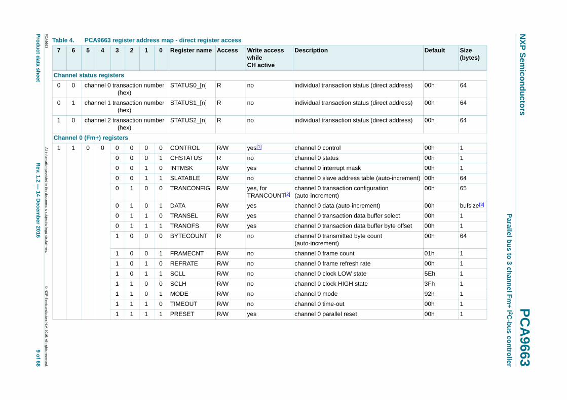
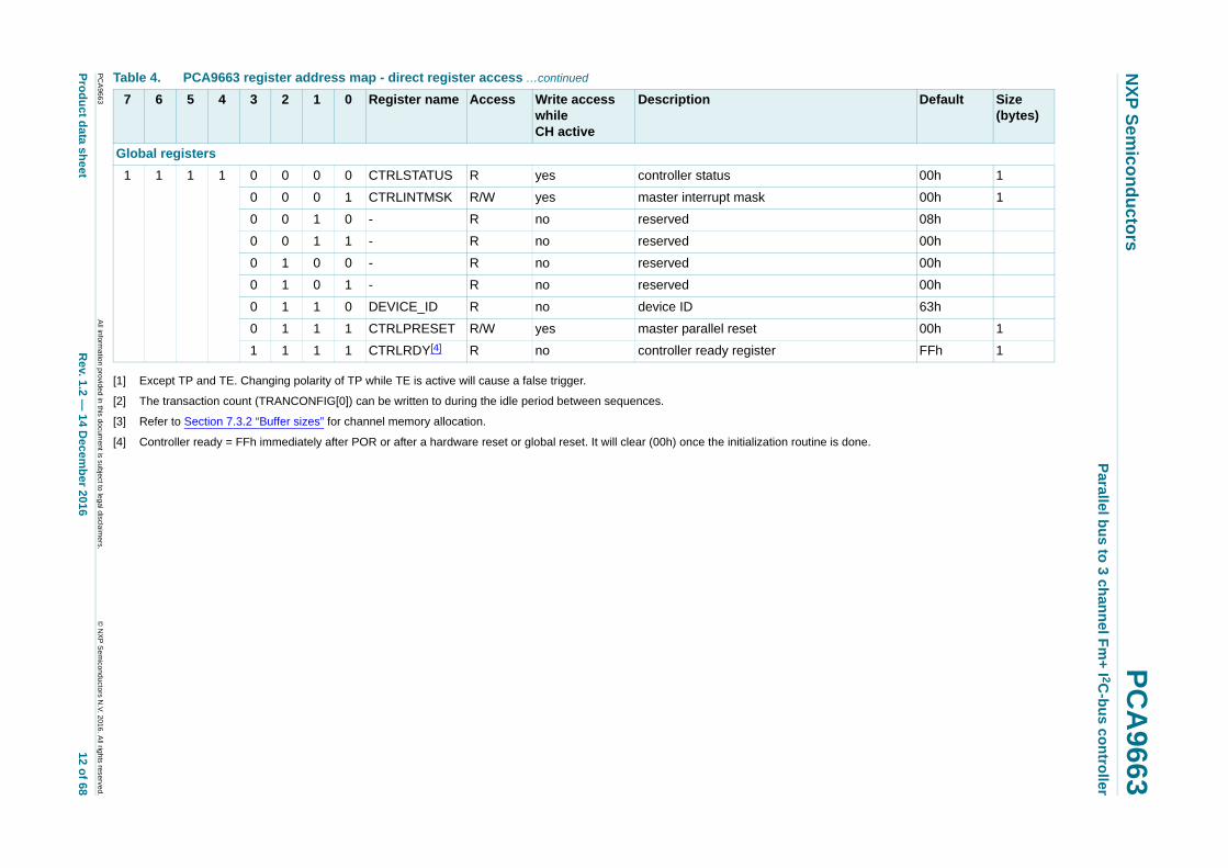
7.5 Registers
The PCA9663 contains several registers that are used to configure the operation of the device, status reporting, and to send and receive data. The device also contains global registers for chip level control and status reporting.
The STATUSx_[n] registers are channel-level direct access registers. The DATA, SLATABLE, TRANCONFIG, and BYTECOUNT registers are auto-increment registers.
The memory access pointer to the DATA registers can be programmed using the TRANSEL and TRANOFS registers. See Section 7.5.1.2 “CONTROL — Control register”, for information on the pointer reset bits BPTRRST and AIPTRRST.
PCA9663 All information provided in this document is subject to legal disclaimers. © NXP Semiconductors N.V. 2016. All rights reserved.
Product data sheet Rev. 1.2 — 14 December 2016 8 of 68
xxxxxxxxxxxxxxxxxxxxx xxxxxxxxxxxxxxxxxxxxxxxxxx xxxxxxx x x x xxxxxxxxxxxxxxxxxxxxxxxxxxxxxx xxxxxxxxxxxxxxxxxxx xx xx xxxxx xxxxxxxxxxxxxxxxxxxxxxxxxxx xxxxxxxxxxxxxxxxxxx xxxxxx xxxxxxxxxxxxxxxxxxxxxxxxxxxxxxxxxxx xxxxxxxxxxxx x x xxxxxxxxxxxxxxxxxxxxx xxxxxxxxxxxxxxxxxxxxxxxxxxxxxx xxxxx xxxxxxxxxxxxxxxxxxxxxxxxxxxxxxxxxxxxxxxxxxxxxxxxxx xxxxxxxx xxxxxxxxxxxxxxxxxxxxxxxxx xxxxxxxxxxxxxxxxxxxx xxx
PC
A966
3
Pro
du
ct data sh
NX
P S
emico
nd
ucto
rsP
CA
9663P
arallel bu
s to 3 ch
ann
el Fm
+ I 2C
-bu
s c
on
troller
Table 4. PCA9663 register address map - direct register access
7 6 5 4 3 2 1 0 Register name Access Write access while CH active
Description Default Size (bytes)
irect address) 00h 64
irect address) 00h 64
irect address) 00h 64
00h 1
00h 1
00h 1
(auto-increment) 00h 64
ation 00h 65
t) 00h bufsize[3]
ffer select 00h 1
ffer byte offset 00h 1
unt 00h 64
01h 1
00h 1
5Eh 1
3Fh 1
92h 1
00h 1
00h 1
All inform
ation provided
in this docum
ent is subject to leg
al disclaim
ers.©
NX
P S
em
iconductors N
.V. 2016. A
ll rights reserved.
eetR
ev. 1.2 — 14 D
ecemb
er 2016 9 o
f 68
Channel status registers
0 0 channel 0 transaction number (hex)
STATUS0_[n] R no individual transaction status (d
0 1 channel 1 transaction number (hex)
STATUS1_[n] R no individual transaction status (d
1 0 channel 2 transaction number (hex)
STATUS2_[n] R no individual transaction status (d
Channel 0 (Fm+) registers
1 1 0 0 0 0 0 0 CONTROL R/W yes[1] channel 0 control
0 0 0 1 CHSTATUS R no channel 0 status
0 0 1 0 INTMSK R/W yes channel 0 interrupt mask
0 0 1 1 SLATABLE R/W no channel 0 slave address table
0 1 0 0 TRANCONFIG R/W yes, for TRANCOUNT[2]
channel 0 transaction configur(auto-increment)
0 1 0 1 DATA R/W yes channel 0 data (auto-incremen
0 1 1 0 TRANSEL R/W yes channel 0 transaction data bu
0 1 1 1 TRANOFS R/W yes channel 0 transaction data bu
1 0 0 0 BYTECOUNT R no channel 0 transmitted byte co(auto-increment)
1 0 0 1 FRAMECNT R/W no channel 0 frame count
1 0 1 0 REFRATE R/W no channel 0 frame refresh rate
1 0 1 1 SCLL R/W no channel 0 clock LOW state
1 1 0 0 SCLH R/W no channel 0 clock HIGH state
1 1 0 1 MODE R/W no channel 0 mode
1 1 1 0 TIMEOUT R/W no channel 0 time-out
1 1 1 1 PRESET R/W yes channel 0 parallel reset

xxxxxxxxxxxxxxxxxxxxx xxxxxxxxxxxxxxxxxxxxxxxxxx xxxxxxx x x x xxxxxxxxxxxxxxxxxxxxxxxxxxxxxx xxxxxxxxxxxxxxxxxxx xx xx xxxxx xxxxxxxxxxxxxxxxxxxxxxxxxxx xxxxxxxxxxxxxxxxxxx xxxxxx xxxxxxxxxxxxxxxxxxxxxxxxxxxxxxxxxxx xxxxxxxxxxxx x x xxxxxxxxxxxxxxxxxxxxx xxxxxxxxxxxxxxxxxxxxxxxxxxxxxx xxxxx xxxxxxxxxxxxxxxxxxxxxxxxxxxxxxxxxxxxxxxxxxxxxxxxxx xxxxxxxx xxxxxxxxxxxxxxxxxxxxxxxxx xxxxxxxxxxxxxxxxxxxx xxx
PC
A966
3
Pro
du
ct data sh
NX
P S
emico
nd
ucto
rsP
CA
9663P
arallel bu
s to 3 ch
ann
el Fm
+ I 2C
-bu
s c
on
troller
Channel 1 (Fm+) registers
00h 1
00h 1
00h 1
(auto-increment) 00h 64
ation 00h 65
t) 00h bufsize[3]
ffer select 00h 1
ffer byte offset 00h 1
unt 00h 64
01h 1
00h 1
5Eh 1
3Fh 1
92h 1
00h 1
00h 1
Table 4. PCA9663 register address map - direct register access …continued
7 6 5 4 3 2 1 0 Register name Access Write access while CH active
Description Default Size (bytes)
All inform
ation provided
in this docum
ent is subject to leg
al disclaim
ers.©
NX
P S
em
iconductors N
.V. 2016. A
ll rights reserved.
eetR
ev. 1.2 — 14 D
ecemb
er 2016 10 o
f 68
1 1 0 1 0 0 0 0 CONTROL R/W yes[1] channel 1 control
0 0 0 1 CHSTATUS R no channel 1 status
0 0 1 0 INTMSK R/W yes channel 1 interrupt mask
0 0 1 1 SLATABLE R/W no channel 1 slave address table
0 1 0 0 TRANCONFIG R/W yes, for TRANCOUNT[2]
channel 1 transaction configur(auto-increment)
0 1 0 1 DATA R/W yes channel 1 data (auto-incremen
0 1 1 0 TRANSEL R/W yes channel 1 transaction data bu
0 1 1 1 TRANOFS R/W yes channel 1 transaction data bu
1 0 0 0 BYTECOUNT R no channel 1 transmitted byte co(auto-increment)
1 0 0 1 FRAMECNT R/W no channel 1 frame count
1 0 1 0 REFRATE R/W no channel 1 frame refresh rate
1 0 1 1 SCLL R/W no channel 1 clock LOW state
1 1 0 0 SCLH R/W no channel 1 clock HIGH state
1 1 0 1 MODE R/W no channel 1 mode
1 1 1 0 TIMEOUT R/W no channel 1 time-out
1 1 1 1 PRESET R/W yes channel 1 parallel reset

xxxxxxxxxxxxxxxxxxxxx xxxxxxxxxxxxxxxxxxxxxxxxxx xxxxxxx x x x xxxxxxxxxxxxxxxxxxxxxxxxxxxxxx xxxxxxxxxxxxxxxxxxx xx xx xxxxx xxxxxxxxxxxxxxxxxxxxxxxxxxx xxxxxxxxxxxxxxxxxxx xxxxxx xxxxxxxxxxxxxxxxxxxxxxxxxxxxxxxxxxx xxxxxxxxxxxx x x xxxxxxxxxxxxxxxxxxxxx xxxxxxxxxxxxxxxxxxxxxxxxxxxxxx xxxxx xxxxxxxxxxxxxxxxxxxxxxxxxxxxxxxxxxxxxxxxxxxxxxxxxx xxxxxxxx xxxxxxxxxxxxxxxxxxxxxxxxx xxxxxxxxxxxxxxxxxxxx xxx
PC
A966
3
Pro
du
ct data sh
NX
P S
emico
nd
ucto
rsP
CA
9663P
arallel bu
s to 3 ch
ann
el Fm
+ I 2C
-bu
s c
on
troller
Channel 2 (Fm+) registers
00h 1
00h 1
00h 1
(auto-increment) 00h 64
ation 00h 65
t) 00h bufsize[3]
ffer select 00h 1
ffer byte offset 00h 1
unt 00h 64
01h 1
00h 1
5Eh 1
3Fh 1
92h 1
00h 1
00h 1
Table 4. PCA9663 register address map - direct register access …continued
7 6 5 4 3 2 1 0 Register name Access Write access while CH active
Description Default Size (bytes)
All inform
ation provided
in this docum
ent is subject to leg
al disclaim
ers.©
NX
P S
em
iconductors N
.V. 2016. A
ll rights reserved.
eetR
ev. 1.2 — 14 D
ecemb
er 2016 11 o
f 68
1 1 1 0 0 0 0 0 CONTROL R/W yes[1] channel 2 control
0 0 0 1 CHSTATUS R no channel 2 status
0 0 1 0 INTMSK R/W yes channel 2 interrupt mask
0 0 1 1 SLATABLE R/W no channel 2 slave address table
0 1 0 0 TRANCONFIG R/W yes, for TRANCOUNT[2]
channel 2 transaction configur(auto-increment)
0 1 0 1 DATA R/W yes channel 2 data (auto-incremen
0 1 1 0 TRANSEL R/W yes channel 2 transaction data bu
0 1 1 1 TRANOFS R/W yes channel 2 transaction data bu
1 0 0 0 BYTECOUNT R no channel 2 transmitted byte co(auto-increment)
1 0 0 1 FRAMECNT R/W no channel 2 frame count
1 0 1 0 REFRATE R/W no channel 2 frame refresh rate
1 0 1 1 SCLL R/W no channel 2 clock LOW state
1 1 0 0 SCLH R/W no channel 2 clock HIGH state
1 1 0 1 MODE R/W no channel 2 mode
1 1 1 0 TIMEOUT R/W no channel 2 time-out
1 1 1 1 PRESET R/W yes channel 2 parallel reset
xxxxxxxxxxxxxxxxxxxxx xxxxxxxxxxxxxxxxxxxxxxxxxx xxxxxxx x x x xxxxxxxxxxxxxxxxxxxxxxxxxxxxxx xxxxxxxxxxxxxxxxxxx xx xx xxxxx xxxxxxxxxxxxxxxxxxxxxxxxxxx xxxxxxxxxxxxxxxxxxx xxxxxx xxxxxxxxxxxxxxxxxxxxxxxxxxxxxxxxxxx xxxxxxxxxxxx x x xxxxxxxxxxxxxxxxxxxxx xxxxxxxxxxxxxxxxxxxxxxxxxxxxxx xxxxx xxxxxxxxxxxxxxxxxxxxxxxxxxxxxxxxxxxxxxxxxxxxxxxxxx xxxxxxxx xxxxxxxxxxxxxxxxxxxxxxxxx xxxxxxxxxxxxxxxxxxxx xxx
PC
A966
3
Pro
du
ct data sh
NX
P S
emico
nd
ucto
rsP
CA
9663P
arallel bu
s to 3 ch
ann
el Fm
+ I 2C
-bu
s c
on
troller
ine is done.
Global registers
00h 1
00h 1
08h
00h
00h
00h
63h
00h 1
FFh 1
Table 4. PCA9663 register address map - direct register access …continued
7 6 5 4 3 2 1 0 Register name Access Write access while CH active
Description Default Size (bytes)
All inform
ation provided
in this docum
ent is subject to leg
al disclaim
ers.©
NX
P S
em
iconductors N
.V. 2016. A
ll rights reserved.
eetR
ev. 1.2 — 14 D
ecemb
er 2016 12 o
f 68
[1] Except TP and TE. Changing polarity of TP while TE is active will cause a false trigger.
[2] The transaction count (TRANCONFIG[0]) can be written to during the idle period between sequences.
[3] Refer to Section 7.3.2 “Buffer sizes” for channel memory allocation.
[4] Controller ready = FFh immediately after POR or after a hardware reset or global reset. It will clear (00h) once the initialization rout
1 1 1 1 0 0 0 0 CTRLSTATUS R yes controller status
0 0 0 1 CTRLINTMSK R/W yes master interrupt mask
0 0 1 0 - R no reserved
0 0 1 1 - R no reserved
0 1 0 0 - R no reserved
0 1 0 1 - R no reserved
0 1 1 0 DEVICE_ID R no device ID
0 1 1 1 CTRLPRESET R/W yes master parallel reset
1 1 1 1 CTRLRDY[4] R no controller ready register

NXP Semiconductors PCA9663Parallel bus to 3 channel Fm+ I2C-bus controller
7.5.1 Channel registers
7.5.1.1 STATUS0_[n], STATUS1_[n], STATUS2_[n] — Transaction status registers
STATUS0_[n], STATUS1_[n], and STATUS2_[n] are 8-bit 64 read-only registers that provide status information for a given transaction. Only the 5 lower bits are used; the top bits will always read 0. When some of these bits are set, a channel interrupt is requested (the INT pin is asserted LOW). A read to STATUSx_[n] register will clear its status. To clear all the STATUSx_[n] registers, a byte-by-byte read of all STATUSx_[n] registers is required. The controller will auto-clear the STATUSx_[n] registers at each START of a sequence when FRAMECNT = 1 and only at the first START when FRAMECNT 1.
Each register byte can be accessed by direct addressing so that the host can choose to read the status on one or more individual transactions without having to read all 64 status bytes.
Remark: When STATUSx_[n] = 00h, no interrupt is requested and the transaction is in the Done/Idle state.
During program execution, the TR and TA bits behave as follows:
Example, we are to transfer 3 transactions in a sequence. All initialization is completed (loading of SLA, TRANCONFIG, DATA) and device is ready for serial transfer.
Before the STA bit is set, the STATUSx_[n] register will contain:
STATUSx_[0] = 0
STATUSx_[1] = 0
STATUSx_[2] = 0
STATUSx_[3] = 0
:
Table 5. STATUSx_[n] - Transaction status code register bit description
Bit Symbol Description
7:5 ST[7:5] always reads 000
4 RSN Read slave NACK. When HIGH, a NACK was received after a slave address was transmitted on the serial bus on a read transaction. An interrupt will be requested.
3 WSN Write slave NACK. When HIGH, a NACK was received after a slave address was transmitted on the serial bus on a write transaction. An interrupt will be requested.
2 WDN Write data NACK. When HIGH, a NACK was received for a data byte during a write transaction on the serial bus. An interrupt will be requested.
1 TA Transaction active. When 1, the transaction is currently active on the serial bus. No interrupt is requested.
0 TR Transaction ready. When 1, a transaction is loaded in the buffer and waiting to be executed. No interrupt is requested.
PCA9663 All information provided in this document is subject to legal disclaimers. © NXP Semiconductors N.V. 2016. All rights reserved.
Product data sheet Rev. 1.2 — 14 December 2016 13 of 68

NXP Semiconductors PCA9663Parallel bus to 3 channel Fm+ I2C-bus controller
After STA is set:
STATUSx_[0] = 2
STATUSx_[1] = 1
STATUSx_[2] = 1
STATUSx_[3] = 0
:
Since there is no timing requirement in setting the STA bit after the initialization, the device will update the first status when the STA bit is set and will always go from 0 to 2 (Idle to Transaction active).
7.5.1.2 CONTROL — Control register
CONTROL is an 8-bit register. The STO bit is affected by the bus controller hardware: it is cleared when a STOP condition is present on the I2C-bus.
Table 6. CONTROL - Control register bit descriptionAddress: Channel 0 = C0h; Channel 1 = D0h; Channel 2 = E0h.Legend: * reset value
Bit Symbol Access Value Description
7 STOSEQ R/W Stop sequence bit.
1 When the STOSEQ bit is set while the channel is active, a STOP condition will be transmitted immediately following the end of the current sequence being transferred on the I2C-bus. No further buffered transactions will be carried out and the channel will return to the idle state. Normal error reporting will occur up until the last bit. When a STOP condition is detected on the bus, the hardware clears the STOSEQ flag.
0 When STOSEQ is reset, no action will be taken.
6 STA R/W The START flag.
1 When the STA bit is set to begin a sequence, the bus controller hardware checks the status of the I2C-bus and generates a START condition if the bus is free. If the bus is not idle, then INT will go LOW and the CHSTATUS register will contain a bus error code (either DAE or CLE will be set).
The STA bit may be set only at a valid idle state. The controller will reset the bit under the following conditions:
• A sequence is done and FRAMECNT = 1.
• A sequence loop is done and FRAMECNT > 1.
• The STOSEQ bit is set, FRAMECNT = 0, and the current sequence is done.
• The STOSEQ bit is set, FRAMECNT > 1, and the current sequence is done.
• The STO bit is set and the current byte transaction is done. This bit cannot be set if the CHEN bit is 0.
0 When the STA bit is reset, no START condition will be generated.
5 STO R/W The STOP flag.
1 When the STO bit is set while the channel is active, a STOP condition will be transmitted immediately following the current data or slave address byte being transferred on the I2C-bus. If a read is in progress, a NACK will be generated before the STOP. No further buffered transactions will be carried out and the channel will return to the idle state. Normal error reporting will occur up until the last bit.
When a STOP condition is detected on the bus, the hardware clears the STO flag.
0 When the STO bit is reset, no action will be taken.
PCA9663 All information provided in this document is subject to legal disclaimers. © NXP Semiconductors N.V. 2016. All rights reserved.
Product data sheet Rev. 1.2 — 14 December 2016 14 of 68

NXP Semiconductors PCA9663Parallel bus to 3 channel Fm+ I2C-bus controller
Remark: Due to a small latency between setting the STA bit and the ability to detect a trigger pulse, if the STA bit is set simultaneously to an incoming trigger pulse, the pulse will be ignored and the controller will wait for the next trigger to send the START.
If the STO or STOSEQ bit are set at anytime while the STA bit is 0, then no action will be taken and the write to these bits is ignored.
Remark: STO has priority over STOSEQ.
4 TP R/W Trigger polarity bit. Cannot be changed while channel is active.
1 Trigger will be detected on a falling edge.
0 Trigger will be detected on a rising edge.
3 TE R/W Trigger Enable (TE) bit controls the trigger input used for frame refresh. TE cannot be changed while channel is active. When the trigger input is enabled, the trigger will override the contents of the FRAMECNT register and will start triggering when STA bit is set. Thereafter, when a trigger tick is detected, the controller will issue a START command and the stored sequence will be transferred on the serial bus.
1 When TE = 1, the sequence is controlled by the Trigger input.
0 When TE = 0, the trigger inputs are ignored.
2 BPTRRST W 1 Resets auto increment pointers for BYTECOUNT. Reads back as 0.
1 AIPTRRST W 1 Resets auto increment pointers for SLATABLE and TRANCONFIG. The DATA register auto-increment pointer will be set to the value that corresponds to TRANSEL and TRANOFS registers. Reads back as 0.
Remark: To reset the data pointer, write 00h to TRANSEL.
0 - W 0 Reserved. User must write 0 to this bit.
Table 6. CONTROL - Control register bit description …continuedAddress: Channel 0 = C0h; Channel 1 = D0h; Channel 2 = E0h.Legend: * reset value
Bit Symbol Access Value Description
PCA9663 All information provided in this document is subject to legal disclaimers. © NXP Semiconductors N.V. 2016. All rights reserved.
Product data sheet Rev. 1.2 — 14 December 2016 15 of 68

NXP Semiconductors PCA9663Parallel bus to 3 channel Fm+ I2C-bus controller
Table 7. CONTROL register bits STA, STO, STOSEQ operation/behavior
Channel state (initialization steps)
Next write action by host Results
FRAMECNT TE STA STO STOSEQ
Idle (reset, TRANCONFIG, SLATABLE, DATA, STA = 0)
1 0 0 X X No action.
1 0 1 X X START transmitted on serial bus followed by sequence stored in buffer.
Active (reset, load TRANCONFIG, SLATABLE, DATA, STA = 1
1 0 X 0 X No change; cannot write STA while active.
1 0 X 1 X When the STO bit is set, two actions are possible:
1. If the transaction is a read, a STOP is sent after the first read byte (NACK sent) and the byte count is updated.
2. If the transaction is a write, a STOP is sent after the end of ACK cycle of the current byte and BYTECNT is updated.
The SD bits will be set.
REFRATE Loop idle (reset, load TRANCONFIG, SLATABLE, DATA STA = 1)[1]
1 0 0 X X No action.
1 0 X 0 1 Channel will go immediately to the inactive state and SD and FLD bits will be set.[2]
1 0 X 1 X Channel will go immediately to the inactive state and SD and FLD bits will be set.[2]
REFRATE Loop active (reset, load, TRANCONFIG, SLATABLE, DATA, STA = 1)
1 0 X 0 0 No action.
1 0 X 0 1 STOP at end of current frame. The SD and FLD bits will be set.
1 0 X 1 X When the STO bit is set, two actions are possible:
1. If the transaction is a read, a STOP is sent after the first read byte (NACK sent) and the byte count is updated.
2. If the transaction is a write, a STOP is sent after the end of ACK cycle of the current byte and BYTECNT is updated.
The SD and FLD bits will be set.
Trigger Loop Idle (reset, load TRANCONFIG, SLATABLE, DATA, STA = 1)
X 1 0 X X No action.
X 1 X 0 1 STOP at end of current frame. The SD and FLD bits will be set.
X 1 X 1 X When the STO bit is set, two actions are possible:
1. If the transaction is a read, a STOP is sent after the first read byte (NACK sent) and the byte count is updated.
2. If the transaction is a write, a STOP is sent after the end of ACK cycle of the current byte and the BYTECNT is updated.
The SD and FLD bits will be set.
PCA9663 All information provided in this document is subject to legal disclaimers. © NXP Semiconductors N.V. 2016. All rights reserved.
Product data sheet Rev. 1.2 — 14 December 2016 16 of 68

NXP Semiconductors PCA9663Parallel bus to 3 channel Fm+ I2C-bus controller
[1] Loop Idle is defined as the time elapsed from a STOP to the START of the next sequence while STA = 1.
[2] Channel Active is defined by the CTRLSTATUS[5:3] bits.
7.5.1.3 CHSTATUS — Channel status register
CHSTATUS is an 8-bit read-only register that provides status information for a given channel. Some of these status bits are error codes that cannot be masked (NMI) by the INTMSK register and need attention from the host. All these status drive the INT pin active LOW. To clear the individual channel interrupt request, you must read the CHSTATUS register. The BE interrupt is cleared by reading the CTRLSTATUS register.
After the CHSTATUS register is cleared, only new errors or status updates will cause the CHSTATUS bits to be set.
The DAE, CLE and SSE bits correspond to bus error states, and the FE bit corresponds to host programming errors.
DAE - SDA error bit: This bit indicates that the SDA line is stuck LOW when the PCA9663 is trying to send a START condition.
CLE - SCL error bit: This bit indicates that the SCL line is stuck LOW.
SSE - illegal START/STOP detected bit: This bit indicates that a bus error has occurred during a serial transfer. A bus error is caused when a START or STOP condition occurs at an illegal position in the format frame. Examples of such illegal positions are during the serial transfer of an address byte, a data byte, or an acknowledge bit. A bus error may also be caused when external interference disturbs the internal PCA9663 signals.
Trigger Loop active (reset, load TRANCONFIG, SLATABLE, DATA, STA = 1)
X 1 X 0 0 No action.
X 1 X 0 1 Channel will go immediately to the inactive state and SD and FLD bits will be set.[2]
X 1 X 1 X Channel will go immediately to the inactive state and SD and FLD bits will be set.[2]
Table 7. CONTROL register bits STA, STO, STOSEQ operation/behavior …continued
Channel state (initialization steps)
Next write action by host Results
FRAMECNT TE STA STO STOSEQ
Table 8. CHSTATUS - Channel and buffer status codes register bit descriptionAddress: Channel 0 = C1h; Channel 1 = D1h; Channel 2 = E1h.
Bit Symbol Description
7 SD Sequence Done. The sequence loaded in the buffer was sent and STOP issued on the serial bus.
6 FLD Frame Loop Done. The FRAMECNT value has been reached. A STOP has been issued on the bus.
5 WE Write Error detected in transaction. An SLA NACK or data NACK was detected in a write transaction of the sequence.
4 RE Read Error detected in transaction. An SLA NACK was detected in a read transaction of the sequence.
3 DAE Bus error, SDA stuck LOW.
2 CLE Bus error, SCL stuck LOW.
1 SSE Bus error, illegal START or STOP detected.
0 FE Frame Error detected. The time required to send the sequence exceeds refresh rate programmed to the REFRATE register or the time between trigger ticks.
PCA9663 All information provided in this document is subject to legal disclaimers. © NXP Semiconductors N.V. 2016. All rights reserved.
Product data sheet Rev. 1.2 — 14 December 2016 17 of 68

NXP Semiconductors PCA9663Parallel bus to 3 channel Fm+ I2C-bus controller
FE - Frame Error bit: This bit indicates that the time required to send the sequence exceeds the refresh rate programmed in the REFRATE register or the time between trigger ticks. Solving frame errors include programming longer refresh rates, speeding up the bus frequency, shortening the amount of bytes sent/received in the sequence, or increasing the time between trigger ticks. If the frame error is masked by the FEMSK, the device will continue to transmit transactions until the end of the sequence without re-starting the sequence even if new triggers are detected. The total number of sequences transmitted will be the number stored in the FRAMECNT register. Once a complete sequence is transmitted, a new sequence will initiate when a subsequent trigger appears. The FE flag will be held HIGH and sequences will still be transmitted unless CHSTATUS is read. If the frame error is unmasked, the sequence will be aborted at the next logical stopping point (i.e., for a read transaction a NACK will be sent), a STOP transmitted and an interrupt will be generated. Since the controller terminates the sequence in a controlled mechanism, there may be a 2-byte delay if a frame error (FE) is detected during a read transaction. The FE bit is set after the STOP is detected on the bus.
a. Sequence fully executed within the period programmed in REFRATE register
This condition causes a frame error and the FE bit to be set.
b. Sequence exceeds period programmed in REFRATE register, FEMSK = 0
c. Sequence exceeds period programmed in REFRATE register, FEMSK = 1
Fig 3. Frame Error detection
002aaf247
sequence A sequence A sequence A
10 ms 10 ms 10 ms
time
002aaf627
sequence B
10 ms 10 ms 10 ms
time
frame error detected, data not sent after FE
002aaf628
sequence C
10 ms 10 ms 10 ms
time
frame error detected, FEMSK = 1, data sent after FE
sequence C
PCA9663 All information provided in this document is subject to legal disclaimers. © NXP Semiconductors N.V. 2016. All rights reserved.
Product data sheet Rev. 1.2 — 14 December 2016 18 of 68
NXP Semiconductors PCA9663Parallel bus to 3 channel Fm+ I2C-bus controller
7.5.1.4 INTMSK — Interrupt mask register
Through the INTMSK register, there is the option to manage which states generate an interrupt, allowing more control from the host on the transaction. The interrupt mask applies to all transactions in a given channel. A bit set to 1 indicates that the mask is active. The INTMSK register default is all interrupts are un-masked (00h).
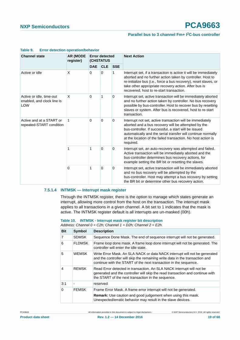
Table 9. Error detection operation/behavior
Channel state AR (MODE register)
Error detected (CHSTATUS
Next Action
DAE CLE SSE
Active or idle X 0 0 1 Interrupt set, if a transaction is active it will be immediately aborted and no further action taken by controller. Host to re-initialize bus (i.e., force a bus recovery), reset slaves, or take other appropriate recovery action. After bus is recovered, host to re-start transaction.
Active or idle, time-out enabled, and clock line is LOW
X 0 1 0 Interrupt set, active transaction will be immediately aborted and no further action taken by controller. No bus recovery possible by bus-controller. Host to recover bus by resetting slaves or system. After bus is recovered, host to re-start transaction.
Active and at a START or repeated-START condition
1 0 0 0 Interrupt not set, active transaction will be immediately aborted and a bus recovery will be attempted by the bus-controller. If successful, a start will be issued automatically and the serial transfer will continue normally at the location of the failed transaction. No host action is required.
1 1 0 0 Interrupt set, an auto-recovery was attempted and failed. Active transaction will be immediately aborted and the bus-controller determines bus recovery actions, for example setting the BR bit or resetting the slaves.
0 1 0 0 Interrupt set, active transaction will be immediately aborted and no bus recovery will be attempted by the bus-controller. Host may attempt a bus recovery by setting the BR bit or determine other bus recovery action.
Table 10. INTMSK - Interrupt mask register bit descriptionAddress: Channel 0 = C2h; Channel 1 = D2h; Channel 2 = E2h.
Bit Symbol Description
7 SDMSK Sequence Done Mask. The end of sequence interrupt will not be generated.
6 FLDMSK Frame loop done mask. A frame loop done interrupt will not be generated. The controller will enter the idle state.
5 WEMSK Write Error Mask. An SLA NACK or data NACK interrupt will not be generated and the controller will skip the remaining write data in the transaction and continue with the START of the next transaction in the sequence.
4 REMSK Read Error detected in transaction. An SLA NACK interrupt will not be generated and the controller will skip the read transaction and continue with the START of the next transaction in the sequence.
3:1 - reserved
0 FEMSK Frame Error Mask. A frame error interrupt will not be generated.
Remark: Use caution and good judgement when using this mask. Unexpected/erratic behavior may result in the slave devices.
PCA9663 All information provided in this document is subject to legal disclaimers. © NXP Semiconductors N.V. 2016. All rights reserved.
Product data sheet Rev. 1.2 — 14 December 2016 19 of 68
NXP Semiconductors PCA9663Parallel bus to 3 channel Fm+ I2C-bus controller
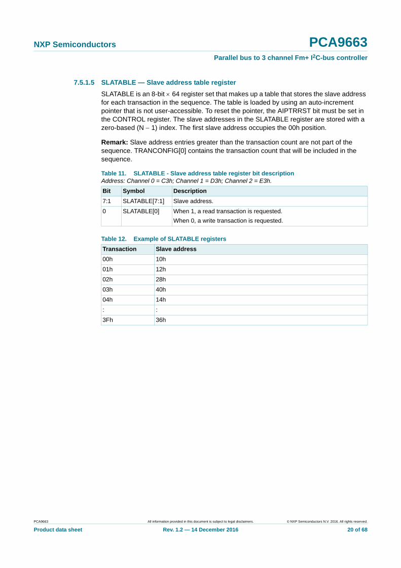
7.5.1.5 SLATABLE — Slave address table register
SLATABLE is an 8-bit 64 register set that makes up a table that stores the slave address for each transaction in the sequence. The table is loaded by using an auto-increment pointer that is not user-accessible. To reset the pointer, the AIPTRRST bit must be set in the CONTROL register. The slave addresses in the SLATABLE register are stored with a zero-based (N 1) index. The first slave address occupies the 00h position.
Remark: Slave address entries greater than the transaction count are not part of the sequence. TRANCONFIG[0] contains the transaction count that will be included in the sequence.
Table 11. SLATABLE - Slave address table register bit descriptionAddress: Channel 0 = C3h; Channel 1 = D3h; Channel 2 = E3h.
Bit Symbol Description
7:1 SLATABLE[7:1] Slave address.
0 SLATABLE[0] When 1, a read transaction is requested.
When 0, a write transaction is requested.
Table 12. Example of SLATABLE registers
Transaction Slave address
00h 10h
01h 12h
02h 28h
03h 40h
04h 14h
: :
3Fh 36h
PCA9663 All information provided in this document is subject to legal disclaimers. © NXP Semiconductors N.V. 2016. All rights reserved.
Product data sheet Rev. 1.2 — 14 December 2016 20 of 68

NXP Semiconductors PCA9663Parallel bus to 3 channel Fm+ I2C-bus controller
7.5.1.6 TRANCONFIG — Transaction configuration register
The TRANCONFIG register is an 8-bit 65 register set that makes up a table that contains the number of transactions that will be executed in a sequence and the number of data bytes involved in the transaction.
The first byte of the register is the Transaction Count register. The remaining 64 registers are the Transaction Length registers.
Remark: Even if the Transaction length (TRANCONFIG[1:40h]) and the SLATABLE([0:3Fh]) are fully initialized, only the specified number of transactions in the Transaction count (TRANCONFIG[0]) will be part of the sequence.
If the Transaction count is 0, then there will be no activity on the serial bus if the STA bit is set. In addition, there will be no interrupts generated or status updated. The controller will simply reset the CONTROL.STA bit without performing any transactions.
If the Transaction length is 0, a read transaction will be skipped and a write transaction will send the slave address plus write bit (SLA+W) on the serial bus with no data bytes.
7.5.1.7 DATA — I2C-bus Data register
DATA is an 8-bit read/write, auto-increment register. It is the interface port to the channel buffer. When accessing the buffer, the host writes a byte of serial data to be transmitted or reads bytes that have just been received at this location. The host can read from the DATA at any time and can only write to this 8-bit register while the channel is idle.
Remark: Reading the DATA when the serial interface is active may return outdated or erroneous data.
The host can read or write data up to the amount of memory space allotted to the channel. The location at which the data is accessed is stored in the TRANSEL and TRANOFS register (both default at 00h).
Table 13. TRANCONFIG, byte 0 - Transaction configuration register bit descriptionAddress: Channel 0 = C4h; Channel 1 = D4h; Channel 2 = E4h.
Bit Symbol Description
7:0 Number of transactions in the sequence. Maximum is 40h.
Table 14. TRANCONFIG, byte 1 to 40h - Transaction configuration register bit description
Bit Symbol Description
7:0 Number of bytes per transaction in the sequence. Maximum is FFh.
Table 15. Example of TRANCONFIG register loaded
Register Value Description
Transaction count 10h 16 transactions = 16 slave addresses in the SLATABLE
Transaction length 00h 0Ah 10 byte transaction
Transaction length 01h 12h 18 byte transaction
Transaction length 02h 28h 40 byte transaction
Transaction length 03h 40h 64 byte transaction
: : :
Transaction length 3Fh 12h 18 byte transaction
PCA9663 All information provided in this document is subject to legal disclaimers. © NXP Semiconductors N.V. 2016. All rights reserved.
Product data sheet Rev. 1.2 — 14 December 2016 21 of 68
NXP Semiconductors PCA9663Parallel bus to 3 channel Fm+ I2C-bus controller
To return to the data location pointed by the contents of the TRANSEL and TRANOFS register after read or write access to the DATA register, set the AIPTRRST (auto-increment pointer reset) bit in the control register.
To return to the first DATA register location in the buffer set the TRANSEL to 00h.
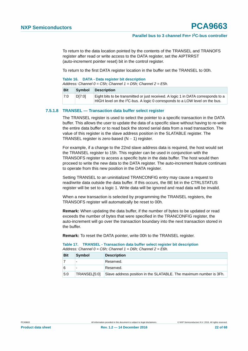
7.5.1.8 TRANSEL — Transaction data buffer select register
The TRANSEL register is used to select the pointer to a specific transaction in the DATA buffer. This allows the user to update the data of a specific slave without having to re-write the entire data buffer or to read back the stored serial data from a read transaction. The value of this register is the slave address position in the SLATABLE register. The TRANSEL register is zero-based (N 1) register.
For example, if a change to the 22nd slave address data is required, the host would set the TRANSEL register to 15h. This register can be used in conjunction with the TRANSOFS register to access a specific byte in the data buffer. The host would then proceed to write the new data to the DATA register. The auto-increment feature continues to operate from this new position in the DATA register.
Setting TRANSEL to an uninitialized TRANCONFIG entry may cause a request to read/write data outside the data buffer. If this occurs, the BE bit in the CTRLSTATUS register will be set to a logic 1. Write data will be ignored and read data will be invalid.
When a new transaction is selected by programming the TRANSEL registers, the TRANSOFS register will automatically be reset to 00h.
Remark: When updating the data buffer, if the number of bytes to be updated or read exceeds the number of bytes that were specified in the TRANCONFIG register, the auto-increment will go over the transaction boundary into the next transaction stored in the buffer.
Remark: To reset the DATA pointer, write 00h to the TRANSEL register.
Table 16. DATA - Data register bit descriptionAddress: Channel 0 = C5h; Channel 1 = D5h; Channel 2 = E5h.
Bit Symbol Description
7:0 D[7:0] Eight bits to be transmitted or just received. A logic 1 in DATA corresponds to a HIGH level on the I2C-bus. A logic 0 corresponds to a LOW level on the bus.
Table 17. TRANSEL - Transaction data buffer select register bit descriptionAddress: Channel 0 = C6h; Channel 1 = D6h; Channel 2 = E6h.
Bit Symbol Description
7 - Reserved.
6 - Reserved.
5:0 TRANSEL[5:0] Slave address position in the SLATABLE. The maximum number is 3Fh.
PCA9663 All information provided in this document is subject to legal disclaimers. © NXP Semiconductors N.V. 2016. All rights reserved.
Product data sheet Rev. 1.2 — 14 December 2016 22 of 68
NXP Semiconductors PCA9663Parallel bus to 3 channel Fm+ I2C-bus controller
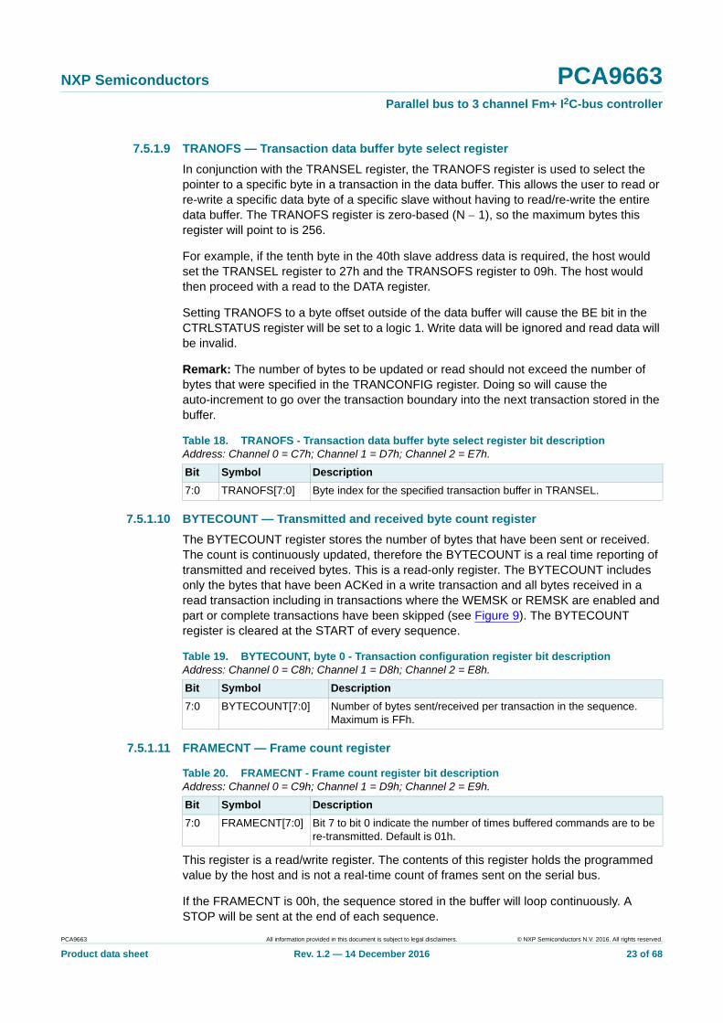
7.5.1.9 TRANOFS — Transaction data buffer byte select register
In conjunction with the TRANSEL register, the TRANOFS register is used to select the pointer to a specific byte in a transaction in the data buffer. This allows the user to read or re-write a specific data byte of a specific slave without having to read/re-write the entire data buffer. The TRANOFS register is zero-based (N 1), so the maximum bytes this register will point to is 256.
For example, if the tenth byte in the 40th slave address data is required, the host would set the TRANSEL register to 27h and the TRANSOFS register to 09h. The host would then proceed with a read to the DATA register.
Setting TRANOFS to a byte offset outside of the data buffer will cause the BE bit in the CTRLSTATUS register will be set to a logic 1. Write data will be ignored and read data will be invalid.
Remark: The number of bytes to be updated or read should not exceed the number of bytes that were specified in the TRANCONFIG register. Doing so will cause the auto-increment to go over the transaction boundary into the next transaction stored in the buffer.
7.5.1.10 BYTECOUNT — Transmitted and received byte count register
The BYTECOUNT register stores the number of bytes that have been sent or received. The count is continuously updated, therefore the BYTECOUNT is a real time reporting of transmitted and received bytes. This is a read-only register. The BYTECOUNT includes only the bytes that have been ACKed in a write transaction and all bytes received in a read transaction including in transactions where the WEMSK or REMSK are enabled and part or complete transactions have been skipped (see Figure 9). The BYTECOUNT register is cleared at the START of every sequence.
7.5.1.11 FRAMECNT — Frame count register
This register is a read/write register. The contents of this register holds the programmed value by the host and is not a real-time count of frames sent on the serial bus.
If the FRAMECNT is 00h, the sequence stored in the buffer will loop continuously. A STOP will be sent at the end of each sequence.
Table 18. TRANOFS - Transaction data buffer byte select register bit descriptionAddress: Channel 0 = C7h; Channel 1 = D7h; Channel 2 = E7h.
Bit Symbol Description
7:0 TRANOFS[7:0] Byte index for the specified transaction buffer in TRANSEL.
Table 19. BYTECOUNT, byte 0 - Transaction configuration register bit descriptionAddress: Channel 0 = C8h; Channel 1 = D8h; Channel 2 = E8h.
Bit Symbol Description
7:0 BYTECOUNT[7:0] Number of bytes sent/received per transaction in the sequence. Maximum is FFh.
Table 20. FRAMECNT - Frame count register bit descriptionAddress: Channel 0 = C9h; Channel 1 = D9h; Channel 2 = E9h.
Bit Symbol Description
7:0 FRAMECNT[7:0] Bit 7 to bit 0 indicate the number of times buffered commands are to be re-transmitted. Default is 01h.
PCA9663 All information provided in this document is subject to legal disclaimers. © NXP Semiconductors N.V. 2016. All rights reserved.
Product data sheet Rev. 1.2 — 14 December 2016 23 of 68

NXP Semiconductors PCA9663Parallel bus to 3 channel Fm+ I2C-bus controller
If the FRAMECNT is 01h, it is defined as the default state and the sequence stored in the buffer will be sent once and a STOP will be sent at the end of the sequence.
If the FRAMECNT is greater than 01h, the sequence stored in the buffer will loop FRAMECNT times and a STOP will be sent at the end of each sequence.
Remark: The FRAMECNT can only be set to loop on the sequence stored in the buffer.
7.5.1.12 REFRATE — Refresh rate register
The REFRATE register defines the time period between each sequence start when REFRATE looping is enabled (FRAMECNT 1, and TE = 0).
The refresh period defined by REFRATE should always be programmed to be greater than the time it takes for the sequence to be transferred on the I2C-bus. If the REFRATE values is too small, the frame error (FE) bit will be set and an interrupt will be requested.
Remark: If the FRAMECNT is 1, then the refresh rate function will be disabled.
7.5.1.13 SCLL, SCLH — Clock rate registers
The clock rate register for the Standard-mode, Fast-mode, and Fast-mode Plus (Fm+) is controlled by the SCLL and SCLH registers. They define the data rate for the serial bus of the PCA9663. The actual frequency on the serial bus is determined by tHIGH (time where SCL is HIGH), tLOW (time where SCL is LOW), tr (rise time), and tf (fall time) values. Writing illegal values into the SCLL and SCLH registers will cause the part to operate at the respective maximum channel frequency.
For Standard, Fast, and Fast-mode Plus, tHIGH and tLOW are calculated based on the values that are programmed into SCLH and SCLL registers and the PLL clock frequency.
Remark: The MODE register needs to be programmed before programming the SCLL and SCLH registers in order to know which I2C-bus mode is selected. See Section 7.5.1.14 “MODE — I2C-bus mode register” for more detail.
Fast-mode Plus (Fm+) is the default selected mode at power-up or after reset.
Table 21. REFRATE - Refresh rate register bit descriptionAddress: Channel 0 = CAh; Channel 1 = DAh; Channel 2 = EAh.
Bit Symbol Description
7:0 REFRATE[7:0] Bit 7 to bit 0 indicate the sequence refresh period. The resolution is 100 s. The default value is 00h, the timer is disabled, and the sequences will be sent back-to-back if the FRAMECNT is = 0 or FRAMECNT is > 1.
Table 22. SCLL - Clock Rate Low register bit description (Standard-mode, Fast-mode, Fast-mode Plus)
Address: Channel 0 = CBh; Channel 1 = DBh; Channel 2 = EBh.
Bit Symbol Description
7:0 L[7:0] Eight bits defining the LOW state of SCL. Default: 94 (5Eh).
Table 23. SCLH - Clock Rate High register bit description (Standard-mode, Fast-mode, Fast-mode Plus)
Address: Channel 0 = CCh; Channel 1 = DCh; Channel 2 = ECh.
Bit Symbol Description
7:0 H[7:0] Eight bits defining the HIGH state of SCL. Default: 63 (3Fh).
PCA9663 All information provided in this document is subject to legal disclaimers. © NXP Semiconductors N.V. 2016. All rights reserved.
Product data sheet Rev. 1.2 — 14 December 2016 24 of 68

NXP Semiconductors PCA9663Parallel bus to 3 channel Fm+ I2C-bus controller
The clock is derived from the internal PLL frequency which is set at 156 MHz (13 OSC clock). Given a 1 % accuracy on the internal clock, the worst case TPLL is
.
Calculating clock settings for Standard, Fast, and Fast-mode Plus:
(1)
The scale factor is set by the MODE register and used in the TOTAL_SCLLH calculation. The scale factor is 8 for Standard-mode, 4 for Fast-mode, and 1 for Fast-mode Plus.
The SCLL and SCLH can be found by:
(2)
(3)
Remark: The contributions for the rise time (tr) and fall time (tf) are adjusted internally by hardware to match the desired frequency. If an invalid number is written to SCLL or SCLH such that it violates the specification, then the controller will adjust the bus frequency to the allowable SCLL and SCLH minimums.
Sample resulting SCL frequencies:
Table 24. SCL frequencies
I2C-bus mode Frequency Scale factor
Standard 100 kHz 8
Fast 400 kHz 4
Fast-mode Plus 1000 kHz 1
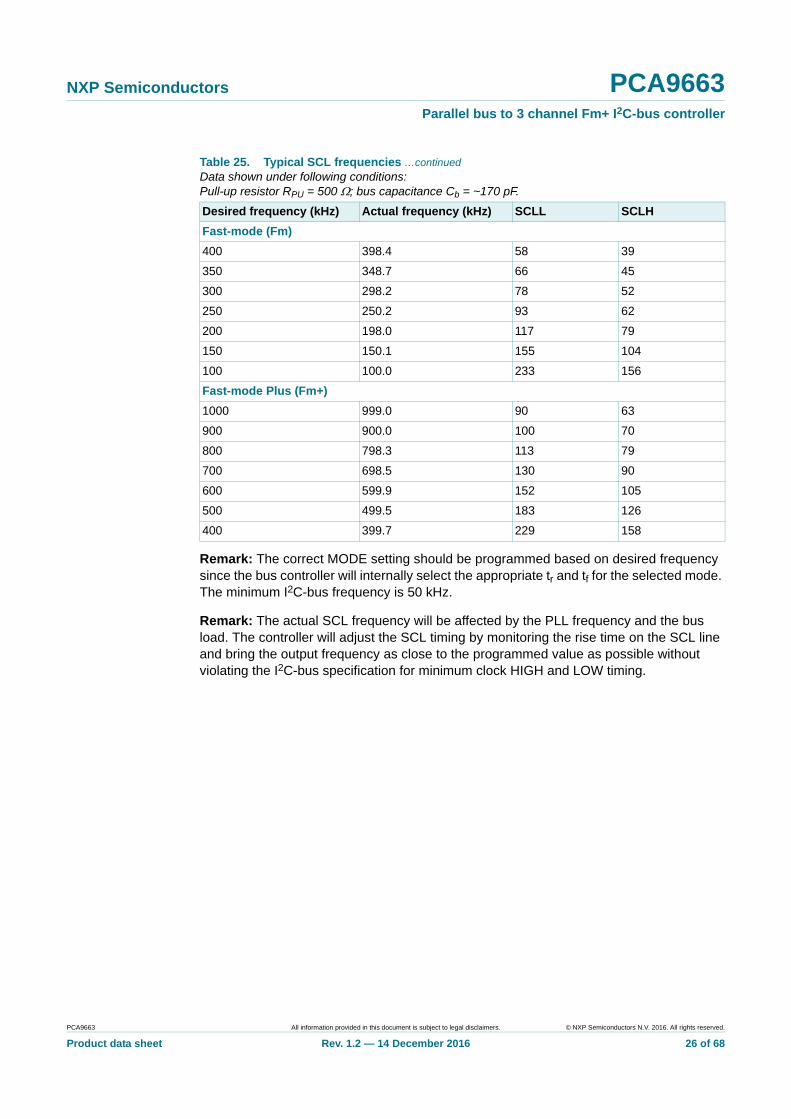
Table 25. Typical SCL frequenciesData shown under following conditions: Pull-up resistor RPU = 500 ; bus capacitance Cb = ~170 pF.
Desired frequency (kHz) Actual frequency (kHz) SCLL SCLH
Standard-mode (Sm)
100 99.3 116 79
90 90.0 129 87
80 80.0 145 98
70 69.5 168 112
60 59.7 194 132
50 50.0 233 156
112.12 MHz 13---------------------------------------- 1
157.56 MHz------------------------------- 6.347 ns= =
TOTAL_SCLLH1
TPLL freq----------------------------- scale factor=
SCLL 0.6 TOTAL _SCLLH=
SCLH 0.4 TOTAL _SCLLH=
PCA9663 All information provided in this document is subject to legal disclaimers. © NXP Semiconductors N.V. 2016. All rights reserved.
Product data sheet Rev. 1.2 — 14 December 2016 25 of 68
NXP Semiconductors PCA9663Parallel bus to 3 channel Fm+ I2C-bus controller
Remark: The correct MODE setting should be programmed based on desired frequency since the bus controller will internally select the appropriate tr and tf for the selected mode. The minimum I2C-bus frequency is 50 kHz.
Remark: The actual SCL frequency will be affected by the PLL frequency and the bus load. The controller will adjust the SCL timing by monitoring the rise time on the SCL line and bring the output frequency as close to the programmed value as possible without violating the I2C-bus specification for minimum clock HIGH and LOW timing.
Fast-mode (Fm)
400 398.4 58 39
350 348.7 66 45
300 298.2 78 52
250 250.2 93 62
200 198.0 117 79
150 150.1 155 104
100 100.0 233 156
Fast-mode Plus (Fm+)
1000 999.0 90 63
900 900.0 100 70
800 798.3 113 79
700 698.5 130 90
600 599.9 152 105
500 499.5 183 126
400 399.7 229 158
Table 25. Typical SCL frequencies …continuedData shown under following conditions: Pull-up resistor RPU = 500 ; bus capacitance Cb = ~170 pF.
Desired frequency (kHz) Actual frequency (kHz) SCLL SCLH
PCA9663 All information provided in this document is subject to legal disclaimers. © NXP Semiconductors N.V. 2016. All rights reserved.
Product data sheet Rev. 1.2 — 14 December 2016 26 of 68

NXP Semiconductors PCA9663Parallel bus to 3 channel Fm+ I2C-bus controller
7.5.1.14 MODE — I2C-bus mode register
MODE is a read/write register. It contains the control bits that select the bus recovery options, and the correct timing parameters. Timing parameters involved with AC[1:0] are tBUF, tHD;STA, tSU;STA, tSU;STO, tHIGH, tLOW. The auto recovery and bus recovery bits are contained in this register. They control the bus recovery sequence as defined in Section 8.5.1 “I2C-bus obstructed by a LOW level on SDA (DAE)”.
Remark: CHEN bit value must be changed only when the I2C-bus is idle.
Remark: Change from an I2C-bus mode to a slower one (Fast-mode to Standard-mode, for example) will cause the HIGH and LOW timings of SCL to be violated. It is then required to program the SCLL and SCLH registers with values in accordance with the selected mode.
Table 26. MODE - I2C-bus mode register bit descriptionAddress: Channel 0 = CDh; Channel 1 = DDh; Channel 2 = EDh.
Bit Symbol Description
7 CHEN Channel Enable bit. R/W.
0: Channel is disabled, SCL and SDA high-impedance. All registers are accessible for setup and configuration, however a sequence cannot be started if the CHEN bit is 0 (STA cannot be set).
1 (default): Channel is enabled.
6 - Reserved.
5 BR Bus Recovery. When BR is set to 1, the bus controller will attempt a bus recovery by sending 9 clock pulses on the bus. Once the bus recovery is complete, the controller will reset the bit to 0. This bit is not intended to generate random or asynchronous 9 clock pulses on the bus. This function is performed automatically when the AR bit is 1.
4 AR Auto Recovery.
When AR = 1 (default), the bus controller will automatically attempt to recover the bus as described in Section 8.5.1 “I2C-bus obstructed by a LOW level on SDA (DAE)”.
When AR = 0, the bus controller will abort the current transaction and generate an error code by setting the DAE bit in the CHSTATUS register and pulling the INT pin LOW.
3:2 - Reserved.
1:0 AC[1:0] I2C-bus mode selection to ensure proper timing parameters (see Table 27 and Table 38).
AC[1:0] = 00: Standard-mode AC parameters selected.
AC[1:0] = 01: Fast-mode AC parameters selected.
AC[1:0] = 10 (default): Fast-mode Plus AC parameters selected.
AC[1:0] = 11: Reserved.
PCA9663 All information provided in this document is subject to legal disclaimers. © NXP Semiconductors N.V. 2016. All rights reserved.
Product data sheet Rev. 1.2 — 14 December 2016 27 of 68

NXP Semiconductors PCA9663Parallel bus to 3 channel Fm+ I2C-bus controller
[1] SCLL and SCLH values in the table also represents the minimum values that can be used for the corresponding I2C-bus mode. Use of lower values will cause the minimum values to be loaded.
[2] Using the formula
7.5.1.15 TIMEOUT — Time-out register
TIMEOUT is an 8-bit read/write register. It is used to determine the maximum time that SCL is allowed to be in a LOW logic state before a CLE interrupt is generated.
When the I2C-bus interface is operating, TIMEOUT is loaded in the time-out counter at every LOW SCL transition.
The Time-out register can be used in the following cases:
• When the bus controller wants to send a START condition and the SCL line is held LOW by some other device. Then the bus controller waits a time period equivalent to the time-out value for the SCL to be released. In case it is not released, the bus controller concludes that there is a bus error, sets the CLE bit in the CHSTATUS register, generates an interrupt signal and releases the SCL and SDA lines.
• The time-out feature starts every time the SCL goes LOW. If SCL stays LOW for a time period equal to or greater than the time-out value, the bus controller concludes there is a bus error and behaves in the manner described above. When the I2C-bus interface is operating, TIMEOUT is loaded in the time-out counter at every SCL transition. See Section 8.7 “Global reset” for more information.
Table 27. I2C-bus mode selection example[1]
SCLL (decimal)
SCLH (decimal)
I2C-bus frequency (kHz)[2]
Scale factor
AC[1:0] Mode
118 79 100 8 00 Standard
59 39 400 4 01 Fast
94 63 1000 1 10 Fast-mode Plus
- - - - 11 reserved
fSCL1
TPLL SCLL SCLH+ sf tr tf+ +-----------------------------------------------------------------------------------------=
Table 28. TIMEOUT - Time-out register bit descriptionAddress: Channel 0 = CEh; Channel 1 = DEh; Channel 2 = EEh.
Bit Symbol Description
7 TE Time-out enable/disable
TE = 1: Time-out function enabled
TE = 0: Time-out function disabled
6:0 TO[6:0] Time-out value. The time-out period = (TIMEOUT[6:0] + 1) 200 s. The time-out value may vary some, and is an approximate value.
PCA9663 All information provided in this document is subject to legal disclaimers. © NXP Semiconductors N.V. 2016. All rights reserved.
Product data sheet Rev. 1.2 — 14 December 2016 28 of 68

NXP Semiconductors PCA9663Parallel bus to 3 channel Fm+ I2C-bus controller
7.5.1.16 PRESET — I2C-bus channel parallel software reset register
PRESET is an 8-bit write-only register. Programming the PRESET register allows the user to reset each individual PCA9663 channel under software control. The software reset is achieved by writing two consecutive bytes to this register. The first byte must be A5h while the second byte must be 5Ah. The writes must be consecutive and the values must match A5h and 5Ah. If this sequence is not followed as described, the reset is aborted.
The PRESET resets state-machines, registers, and buffer pointers to the default values, zeroes the TRANCONFIG, SLATABLE, BYTECOUNT, and DATA arrays of the respective channel and will not reset the entire chip. The parallel bus remains active while a software reset is active. The user can read the PRESET register to determine when the reset has completed, PRESET returns all 1s when the reset is active and all 0s when complete.
7.5.2 Global registers
7.5.2.1 CTRLSTATUS — Controller status register
The CTRLSTATUS register reports the status of the controller, including the interrupts generated by the parallel bus. There are six status bits. When CTRLSTATUS contains 00h, it indicates the idle state and therefore no serial interrupts are requested. The content of this register is continuously updated during the operation of the controller.
The lower 3 bits represent the channels that have an interrupt request pending. To clear the individual channel interrupt request, you must read the CHSTATUS register. Bits [5:3] indicate if a channel is currently active or if it is in the idle state.
Remark: A global reset will reset all channels and configuration settings.
BE - Buffer Error bit: This bit indicates that a buffer error has been detected. For example, a buffer overflow due to the host programming too many bytes will set this bit. A software or hardware reset is necessary to recover from a buffer error.
Table 29. PRESET - I2C-bus channel parallel software reset register bit descriptionAddress: Channel 0 = CFh; Channel 1 = DFh; Channel 2 = EFh.
Bit Symbol Description
7:0 PRESET[7:0] Write-only register used during an I2C-bus channel parallel reset command.
Table 30. CTRLSTATUS - Interrupt status register bit descriptionAddress: F0h.
Bit Symbol Description
7 BE Buffer Error. A buffer error such as overflow has been detected.
6 -
5 CH2ACT Channel 2 is active.
4 CH1ACT Channel 1 is active.
3 CH0ACT Channel 0 is active.
2 CH2INTP Channel 2 interrupt pending.
1 CH1INTP Channel 1 interrupt pending.
0 CH0INTP Channel 0 interrupt pending.
PCA9663 All information provided in this document is subject to legal disclaimers. © NXP Semiconductors N.V. 2016. All rights reserved.
Product data sheet Rev. 1.2 — 14 December 2016 29 of 68

NXP Semiconductors PCA9663Parallel bus to 3 channel Fm+ I2C-bus controller
The buffer error may occur when a data location is being read or written to that has not previously been configured by the TRANCONFIG register. The buffer error can occur on a parallel data write or read beyond the buffer capacity, or setting the TRANSEL and TRANOFS pointers beyond the buffer boundary.
When the DATA register is loaded with data that goes beyond the capacity of the buffer, the bytes that go over the buffer size will be ignored and a Buffer Error (BE) will be generated.
Special case: The BE interrupt is cleared by reading the CTRLSTATUS register. All other interrupts are cleared by reading the respective CHSTATUS register.
Fig 4. PCA9663 status reporting logic
002aaf456
DAE
CLE
SSE
SD
WE
RE
FE
FLD
CH0INTP
DAE
CLE
SSE
SD
WE
RE
FE
FLD
CH1INTP
DAE
CLE
SSE
SD
WE
RE
FE
FLD
CH2INTP
PCA9663 All information provided in this document is subject to legal disclaimers. © NXP Semiconductors N.V. 2016. All rights reserved.
Product data sheet Rev. 1.2 — 14 December 2016 30 of 68

NXP Semiconductors PCA9663Parallel bus to 3 channel Fm+ I2C-bus controller
7.5.2.2 CTRLINTMSK — Control Interrupt mask register
The CTRLINTMSK masks all interrupts generated by the masked channel. This allows the host MCU to complete other operations before servicing the interrupt without being interrupted by the same channel.
Table 31. CTRLINTMSK - Control interrupt mask register bit descriptionAddress: F1h.
Bit Symbol Description
7 BEMSK Buffer Error Mask. A buffer error interrupt will not be generated.
Remark: Use caution and good judgement when using this mask. Unexpected/erratic behavior may result in the slave devices.
6:3 - reserved
2 CH2MSK When this bit is set to 1, all interrupts for the channel will be masked and the INT pin will not be pulled LOW.
1 CH1MSK When this bit is set to 1, all interrupts for the channel will be masked and the INT pin will not be pulled LOW.
0 CH0MSK When this bit is set to 1, all interrupts for the channel will be masked and the INT pin will not be pulled LOW.
PCA9663 All information provided in this document is subject to legal disclaimers. © NXP Semiconductors N.V. 2016. All rights reserved.
Product data sheet Rev. 1.2 — 14 December 2016 31 of 68

NXP Semiconductors PCA9663Parallel bus to 3 channel Fm+ I2C-bus controller
7.5.2.3 DEVICE_ID — Device ID
The DEVICE_ID register stores the bus controller part number so it can be identified on the parallel bus.
Fig 5. PCA9663 interrupt logic
SDSDMSK
WEWEMSK
REREMSK
FEFEMSK
FLDFLDMSK
DAE
CLE
SSE
CH0MSK
CH0 interruptsources and masks
DAE
CLE
SSE
CH1MSK
CH1 interruptsources and masks
DAE
CLE
SSE
CH2MSK
CH2 interruptsources and masks
to INT pin
BEMSKBE
SDSDMSK
WEWEMSK
REREMSK
FEFEMSK
FLDFLDMSK
SDSDMSK
WEWEMSK
REREMSK
FEFEMSK
FLDFLDMSK
002aaf147
Table 32. DEVICE_ID - Device ID register bit descriptionAddress: F6h.
Bit Symbol Description
7 U/A Selects PCU or PCA device.
1 = PCU96xx
0 = PCA96xx
6:0 BCD BCD (Binary Coded Decimal) code of the ending 2 digits for ID. Range is 00h to 79h. The code for the PCA9663 is 63h.
PCA9663 All information provided in this document is subject to legal disclaimers. © NXP Semiconductors N.V. 2016. All rights reserved.
Product data sheet Rev. 1.2 — 14 December 2016 32 of 68

NXP Semiconductors PCA9663Parallel bus to 3 channel Fm+ I2C-bus controller
7.5.2.4 CTRLPRESET — Parallel software reset register
CTRLPRESET is an 8-bit write-only register. Programming the CTRLPRESET register allows the user to reset the PCA9663 under software control. The software reset is achieved by writing two consecutive bytes to this register. The first byte must be A5h while the second byte must be 5Ah. The writes must be consecutive and the values must match A5h and 5Ah. If this sequence is not followed as described, the reset is aborted.
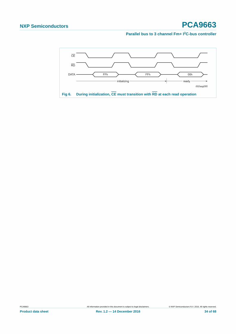
7.5.2.5 CTRLRDY — Controller ready register
CTRLRDY (address FFh) is an 8-bit read-only register. It indicates the internal state of the controller. When the register is FFh, the controller is in the initialization state. The initialization state will be entered at power-up, after a hardware reset, or after a global software reset.
The oscillator and the PLL will be initialized only after a Power-On Reset (POR), a hardware reset, or a global software reset (CTRLPRESET).
When the register is 00h, the controller is in the normal operating mode.
Access while the controller is initializing requires CE pin follow the RD pin transitions to update the state of the controller that is read back. After controller is ready, the CE pin can be held LOW while RD and WR pins transition. See Figure 6, Figure 7 and Figure 8.
Table 33. CTRLPRESET - Parallel software reset register bit descriptionAddress: F7h.
Bit Symbol Description
7:0 CTRLPRESET[7:0] Write-only register used during a device parallel reset command.
Table 34. CTRLRDY - Controller ready register bit descriptionAddress: FFh.
Bit Symbol Description
7:0 CTRLRDY[7:0] Read-only register indicates the internal state of the controller. FFh indicates the controller is initializing, 00h indicates controller is in normal operating mode.
PCA9663 All information provided in this document is subject to legal disclaimers. © NXP Semiconductors N.V. 2016. All rights reserved.
Product data sheet Rev. 1.2 — 14 December 2016 33 of 68
NXP Semiconductors PCA9663Parallel bus to 3 channel Fm+ I2C-bus controller
Fig 6. During initialization, CE must transition with RD at each read operation
002aag095
CE
00hFFhFFh
initializing ready
RD
DATA
PCA9663 All information provided in this document is subject to legal disclaimers. © NXP Semiconductors N.V. 2016. All rights reserved.
Product data sheet Rev. 1.2 — 14 December 2016 34 of 68

NXP Semiconductors PCA9663Parallel bus to 3 channel Fm+ I2C-bus controller
8. PCA9663 operation
The PCA9663 is designed to efficiently transmit and receive large amounts of data on a single master bus. There are three major components that compose the architecture of the I2C-bus controller that interact with each other to provide a high throughput and a high level of automation when it conducts transactions:
• Slave address table: specifies the address of the slaves on the bus and the direction (read or write).
• Transaction configuration: specifies the size of the transaction.
• Data buffer: contains the data to be transmitted or received from the slave.
These three components are integrated in the PCA9663 to build a sequence. A sequence is a set of read or write transactions and the minimum sequence size is one read or write transaction. Several transactions can be stored in one sequence and be executed without the intervention of the host controller (CPU) through loop control and using the built-in refresh rate timers.
The PCA9663 executes transactions in the order they were loaded into the buffer without interrupting the host. Once the end of a sequence is reached, the Sequence Done (SD) bit will be asserted in the CHSTATUS register and the controller will request an interrupt, if SDMSK = 0. At this point, the host can reload the buffer with a new sequence or resend the one that is currently loaded in the buffer.
When a sequence is in progress, no interrupts are generated unless there is an error when a transaction is conducted. The host will only receive an interrupt when the sequence is done. The PCA9663 will dynamically shift between being a Master
Fig 7. During normal operation, CE may remain LOW while RD transitions during multiple reads
Fig 8. During normal operation, CE may remain LOW while WR transitions during multiple writes
002aag096
CE
address Zaddress Yaddress X
RD
DATA
read address Zread address Yread address XADDR
002aag097
CE
data Zdata Ydata X
WR
DATA
write address Zwrite address Ywrite address XADDR
PCA9663 All information provided in this document is subject to legal disclaimers. © NXP Semiconductors N.V. 2016. All rights reserved.
Product data sheet Rev. 1.2 — 14 December 2016 35 of 68
NXP Semiconductors PCA9663Parallel bus to 3 channel Fm+ I2C-bus controller
Transmitter or a Master Receiver according to the direction bits specified in the SLATABLE. The host has the ability to retrieve stored serial data as soon as a read transaction is done, while the controller carries on the remaining transactions in the sequence.
8.1 Sequence execution
Sequences can have transactions of two types:
• Write transactions, where the PCA9663 will behave as a Master Transmitter
• Read transactions, where the PCA9663 will behave as a Master Receiver
Data transfers in each direction are shown in Figure 9. This figure contains the following abbreviations:
S — START condition
SLA — 7-bit slave address
R — Read bit (HIGH level at SDA)
W — Write bit (LOW level at SDA)
A — Acknowledge bit (LOW level at SDA)
A — Not acknowledge bit (HIGH level at SDA)
Data — 8-bit data byte
P — STOP condition
In Figure 9, circles are used to indicate when a bit is set in the CHSTATUS register. A channel interrupt is not requested when CHSTATUS = 00h and the INT pin is not asserted when the interrupt is masked (see Section 7.5.2.2).
For a successful sequence execution, all three components mentioned above must exist in the memory and must be correctly set up. There are not safeguards against programming incorrect transaction sizes, data buffer lengths, or direction bits. If the transaction length is set to 00h, then only the slave address with direction bit will be transmitted.
Once the host has configured the serial port and programmed the TRANCONFIG (number of slaves and bytes per slave), the SLATABLE (slave addresses), TRANSEL (transaction data buffer selection) and the TRANOFS (byte offset selection) and loaded the serial data into the DATA buffer, the sequence is ready to be transmitted.
To send the sequence, the host will set the STA bit in the CONTROL register and the controller will immediately send a START on the serial bus. Then, the transactions will be carried out in the order they appear in the SLATABLE, each being separated by a ReSTART command.
If the interrupts are unmasked, the serial transfer will be conducted without generating interrupts in between transactions. Once all transactions are successfully completed, the controller will generate a STOP, the Sequence Done bit (SD) will be set in the CHSTATUS and an interrupt will be generated.
PCA9663 All information provided in this document is subject to legal disclaimers. © NXP Semiconductors N.V. 2016. All rights reserved.
Product data sheet Rev. 1.2 — 14 December 2016 36 of 68

NXP Semiconductors PCA9663Parallel bus to 3 channel Fm+ I2C-bus controller
When the interrupts are unmasked, a NACK on slave address or data (in a write cycle) will terminate the serial transfer, generate a STOP, and the INT pin will be asserted. The host can read the CTRLSTATUS (Controller status register) to determine which channel generated the interrupt, then it can read the CHSTATUS register of the channel and the STATUSx_[n] to determine which slave address caused the error.
If the interrupts WEMSK and REMSK are set, then a NACK on slave address or data (in a write cycle) will not terminate the serial transfer, the error will be stored in the STATUSx_[n] register and the serial transfer will continue with the next transaction in the sequence. Once all transactions are completed, the controller will generate a STOP and the Sequence Done bit (SD) and other error bits (WE or RE) will be set in the CHSTATUS and an interrupt will be generated.
If the host wants to poll the PCA9663, it can mask all registers including the SD bit and read the CTRLSTATUS, CHSTATUS, STATUSx_[n], and/or the CONTROL registers to determine the state of the controller.
PCA9663 All information provided in this document is subject to legal disclaimers. © NXP Semiconductors N.V. 2016. All rights reserved.
Product data sheet Rev. 1.2 — 14 December 2016 37 of 68

xxxxxxxxxxxxxxxxxxxxx xxxxxxxxxxxxxxxxxxxxxxxxxx xxxxxxx x x x xxxxxxxxxxxxxxxxxxxxxxxxxxxxxx xxxxxxxxxxxxxxxxxxx xx xx xxxxx xxxxxxxxxxxxxxxxxxxxxxxxxxx xxxxxxxxxxxxxxxxxxx xxxxxx xxxxxxxxxxxxxxxxxxxxxxxxxxxxxxxxxxx xxxxxxxxxxxx x x xxxxxxxxxxxxxxxxxxxxx xxxxxxxxxxxxxxxxxxxxxxxxxxxxxx xxxxx xxxxxxxxxxxxxxxxxxxxxxxxxxxxxxxxxxxxxxxxxxxxxxxxxx xxxxxxxx xxxxxxxxxxxxxxxxxxxxxxxxx xxxxxxxxxxxxxxxxxxxx xxx
PC
A966
3
Pro
du
ct data sh
NX
P S
emico
nd
ucto
rsP
CA
9663P
arallel bu
s to 3 ch
ann
el Fm
+ I 2C
-bu
s c
on
troller
80h
P
002aag293
SLA 0S W A DATA SLA 0 R DATA A DATA A SSLA 1 W DATAn SLA n
transactions with WEMSK and REMSK = 0
00h
A A S A A S W DATAn
20h
A
A P
08h
20h
A
A P
04h
P
80h
00h
S
SLA n
h
W
20h
A
A
08h
DATAn A
E0hC0hA0h
C0h
All inform
ation provided
in this docum
ent is subject to leg
al disclaim
ers.©
NX
P S
em
iconductors N
.V. 2016. A
ll rights reserved.
eetR
ev. 1.2 — 14 D
ecemb
er 2016 38 o
f 68
Example CHSTATUS codes:
80h: sequence done with no errors
C0h: frame loop and sequence done with no errors
A0h: sequence done with a write error
D0h: frame loop and sequence done with a read error
Fig 9. PCA9663 I2C status codes
CHSTATUS register, interrupt requested; interrupt goes LOW at the STOP
DATA A any number of data bytes and their associated Acknowledge bits
from master to slave
from slave to master
STATUSx_[n] register, no interrupt
A last byte is NACK
SLA 0S W A
A
DATA S SLA 0 R
01h
DATA A DATA A
n
S W
transactions with WEMSK and REMSK = 1
20h
Adata availableto be read onparallel bus
P
01h 08h
20h
A P
04h
10h
A P
10h
20h
A P
F8h
20h
A P
04h
20h
08h
20h
A
A
04h
02h
10h
A
A
10h data availableto be read onparallel bus
02h
SLA 1
20h
A
A
08h
DATAn A SS
02h
02
01h
01h

xxxxxxxxxxxxxxxxxxxxx xxxxxxxxxxxxxxxxxxxxxxxxxx xxxxxxx x x x xxxxxxxxxxxxxxxxxxxxxxxxxxxxxx xxxxxxxxxxxxxxxxxxx xx xx xxxxx xxxxxxxxxxxxxxxxxxxxxxxxxxx xxxxxxxxxxxxxxxxxxx xxxxxx xxxxxxxxxxxxxxxxxxxxxxxxxxxxxxxxxxx xxxxxxxxxxxx x x xxxxxxxxxxxxxxxxxxxxx xxxxxxxxxxxxxxxxxxxxxxxxxxxxxx xxxxx xxxxxxxxxxxxxxxxxxxxxxxxxxxxxxxxxxxxxxxxxxxxxxxxxx xxxxxxxx xxxxxxxxxxxxxxxxxxxxxxxxx xxxxxxxxxxxxxxxxxxxx xxx
PC
A966
3
Pro
du
ct data sh
NX
P S
emico
nd
ucto
rsP
CA
9663P
arallel bu
s to 3 ch
ann
el Fm
+ I 2C
-bu
s c
on
troller
002aaf620
byte 0
byte 0
byte 1
byte 2
byte 4
byte 0
byte 1
byte 15
ta byte 0
ta byte 1
ta byte 7
internal memory pointerA00h or F00h
sequence read and write data memory space
internal memory pointer0000h
anaged troller.
byte 3
All inform
ation provided
in this docum
ent is subject to leg
al disclaim
ers.©
NX
P S
em
iconductors N
.V. 2016. A
ll rights reserved.
eetR
ev. 1.2 — 14 D
ecemb
er 2016 39 o
f 68
Status and configuration registers are not shown.
Shaded areas are comments/indexes that are not user-accessible.
Fig 10. PCA9663 sequence block diagram; sample sequence loaded
00h
TRANCONFIG
-
01h
02h
:
03h
3Dh
3Eh
3Fh
01h
40h
05h
10h
:
08h
10h
05h
08h
Transaction count
Transaction 0 length, 1 byte
Transaction 1 length, 5 bytes
Transaction 2 length, 16 bytes
Transaction 3 length, 8 bytes
:
Transaction 61 length, 16 bytes
Transaction 62 length, 5 bytes
Transaction 63 length, 8 bytes
00h
SLATABLE
01h
02h
:
03h
3Dh
3Eh
3Fh
10h
11h
40h
:
E0h
20h
33h
20h
SLAW
SLAR
SLAW
SLAW
:
SLAW
SLAR
SLAW
The slave address plus transaction count, direction bit, the transaction length and the transaction data make up one complete serial bus transaction or sequence.
DATA
00h
10h
00h
00h
00h
02h
55h
Transaction 0, data
Transaction 1, data
Transaction 1, data
Transaction 1, data
Transaction 1, data
Transaction 2, data
Transaction 2, data
:
AAh
:
Transaction 2, data
: :
44h Transaction 63, da
AAh Transaction 63, da
: :
55h Transaction 63, da
: :
: :
: :
: :
unusedmemory
space
The memory pointers are minternally by the buffer con
number of slave addressesto be included in a sequence
00h Transaction 1, data
transaction lengthcorresponding to eachslave address in theSLATABLE
slave addressplus direction bit
NXP Semiconductors PCA9663Parallel bus to 3 channel Fm+ I2C-bus controller
8.2 Read transactions
Many I2C-bus slave devices need a command or register offset to setup a read operation. In this case, a read transaction is actually a multi-part transaction consisting of a write transaction followed by a read transaction. This is done by setting the transactions in that order when programming the sequence.
If no write is required prior to a read, then the read transaction can be placed in any location of the sequence. Once the read transaction is completed (i.e., the TR bit is cleared to 0) the data is immediately available for the host to retrieve it on the parallel bus.
8.3 Stopping a sequence
If the host needs to stop the execution of a sequence, it should set the STO bit in the CONTROL register. For write transactions, the host will issue a STOP after the acknowledge cycle of the current byte being transferred on the serial bus. For read transactions, if the host sets the STO bit while an address + read bit (SLA+R) is sent, the controller will complete the read of one byte by sending 9 clocks and a NACK on the ninth clock before sending the STOP condition. If the host sets the STO bit while a read transaction is in progress, the current byte will be NACKed before sending a STOP condition. No interrupts will be generated and all the status registers will be up to date. The Sequence Done bit (SD) will be set to indicate to the host that the STOP condition was completed and the bus is idle. The Sequence Done and the Frame Loop Done will be set if the channel is in Loop mode (FRAMECNT 1) and a STO or STOSEQ bit is set.
If the host issues a STOP (by setting the STO) in the middle of a sequence followed by a START (by setting the STA), then the controller will re-send the sequence from the beginning, not from the point where the sequence was last stopped.
8.4 Looping a sequence
A sequence can be set to automatically loop several times using the FRAMECNT and one of the following:
• The REFRATE register. The REFRATE register contains the value of the refresh rate which is timing required between the START of two sequences. The refresh rate is derived from the internal clock of the bus controller. If the REFRATE is programmed to 00h, the sequences will be looped back-to-back.
• Trigger enable (TE) bit. When TE is set, the refresh rate is controlled by the external trigger input and the contents of the REFRATE registers is ignored. There is no maximum timing requirement for the trigger interval.
The FRAMECNT register sets the number of times the sequence will be repeated. A frame is defined as a sequence associated with its respective refresh rate. As described above, the frame refresh rate is determined by the REFRATE register or an external trigger source.
During looping, there is no host intervention required and all status and error reporting remains active. The SD (Sequence Done) bit can be masked to avoid getting interrupted each time a frame is completed while the other error reporting bits remain unmasked. In this manner, normal transactions can run without host intervention and errors will be reported at the STOP of the current byte where the error occurred.
PCA9663 All information provided in this document is subject to legal disclaimers. © NXP Semiconductors N.V. 2016. All rights reserved.
Product data sheet Rev. 1.2 — 14 December 2016 40 of 68

NXP Semiconductors PCA9663Parallel bus to 3 channel Fm+ I2C-bus controller
Once the FRAMECNT values is reached, the FLD bit in the CHSTATUS register is set and no further transactions will be executed and the channel will go to the idle state. The FLD interrupt can be masked with the FLDMSK bit in the CTRLINTMSK register. The host can poll the CTRLSTATUS register to check if the channel is active (looping) or if it is idle.
For indefinite or long term looping the host can do the following:
1. A sequence can be set to loop indefinitely by setting the FRAMECNT register to 00h. Each frame will be sent out following the REFRATE settings or the Trigger input if the TE bit is set. To end the Loop mode, the host sets the STO or STOSEQ bits in the CONTROL register.
2. A frame will be sent out continuously and back-to-back if FRAMECNT and REFRATE are set to 00h. To end the Loop mode, the hose sets the STO or STOSEQ bits in the CONTROL register.
8.4.1 Looping with REFRATE control
When using the REFRATE register (TE bit is 0) the refresh rate timing is controlled internally. Once the STA bit is set, the START command will be immediately sent on the serial bus followed by the sequence. Thereafter, the controller will issue a START command followed by the stored sequence every time the REFRATE value is reached. It is important to program enough time in the REFRATE to allow a complete sequence to reach the Sequence Done state. If the refresh rate is not long enough, the Frame Error (FE) bit will be set and an interrupt will be generated. The FE bit is maskable, however, masking the FE bit may yield undesired results on the serial interface. If the FE bit is masked, the Loop mode will continue to operate and the FE flag will remain set. To exit the Loop mode, the STO or the STOSEQ bit should be set.
8.4.2 Looping with Trigger control
The PCA9663 has one trigger input. The trigger enable (TE) bit in the CONTROL register is used to control the use of external triggering. Once enabled, the trigger will override the contents of the REFRATE register, and will start triggering when the STA bit is set. Therefore, a significant time delay can occur between setting the STA bit and the detection of a trigger. When a trigger edge is detected, the controller will issue a START command and the stored sequence will be transferred on the serial bus. The trigger will control the timing of the frame, therefore, enough time should be allowed by the trigger to allow the sequence to reach the Sequence Done state.
If a trigger edge is detected while a sequence is actively being transmitted on the bus, the Frame Error (FE) bit will be set and an interrupt will be generated. The FE bit is maskable, however, masking the FE bit may yield undesired results on the serial interface. If the FE bit is masked, the Loop mode will continue to operate and the FE flag will remain set. The polarity of the trigger edge detect is controlled by the TP bit in the CONTROL register. To exit the Trigger mode, the STO or the STOSEQ bit should be set.
PCA9663 All information provided in this document is subject to legal disclaimers. © NXP Semiconductors N.V. 2016. All rights reserved.
Product data sheet Rev. 1.2 — 14 December 2016 41 of 68
NXP Semiconductors PCA9663Parallel bus to 3 channel Fm+ I2C-bus controller
8.5 Bus errors
Bus errors are a rare occurrence in a well designed I2C-bus system. The PCA9663 has a robust error detection mechanism that detects hang-ups such as if SDA or SCL is pulled LOW by an external source, or if an illegal START or STOP condition appears on the bus.
8.5.1 I2C-bus obstructed by a LOW level on SDA (DAE)
An I2C-bus hang-up occurs if SDA is pulled LOW by an uncontrolled source (e.g., a slave device out of bit synchronization). If the SDA line is obstructed by another device on the bus, the problem can be solved by transmitting additional clock pulses on the SCL line (see Figure 11). The SDA stuck fault detection is only active during a START or repeated-START condition.
When the error is detected, if the auto-recovery bit is set (AR = 1), the PCA9663 sends out nine clock pulses followed by the STOP condition (see Figure 11). If the SDA line is released by the slave pulling it LOW, a normal START condition is transmitted by the PCA9663, the TA bit is set in the STATUSx_[n] register and the serial transfer continues. If the SDA line is not released by the slave pulling it LOW, then the PCA9663 concludes that there is a bus error, sets the DAE bit in the CHSTATUS register, generates an interrupt signal, and releases the SCL and SDA lines.
If the auto-recovery bit is reset (AR = 0) during error detection, the PCA9663 loads the bus error (sets the DAE bit in the CHSTATUS register), generates an interrupt signal, and releases the SCL and SDA lines. After the host reads the status register, it can force a bus recovery sequence by setting the bus recovery bit to 1 (BR = 1). The PCA9663 will transmit additional clock pulses on the SCL line and the host must re-start the transmission by setting the STA bit.
If a repeated START condition is transmitted while SDA is obstructed (pulled LOW), the PCA9663 performs the same action as described above. In each case, the TA bit is set after a successful START condition is transmitted and normal serial transfer continues. Note that the host is not involved in solving these bus hang-up problems when the auto-recovery bit is set (AR = 1).
When a host is unable to recover the bus by having the AR bit set or forcing a bus recovery sequence by setting the bus recovery by setting the BR, then it may be necessary to reset the slaves or the system.
Remark: If the AR bit is set and an SDA stuck LOW is detected, the transaction will continue normally after an auto-recovery from the failed location in the sequence. If the AR bit is zero and a manual bus recovery is performed, the transaction will be re-started from the beginning of the sequence.
PCA9663 All information provided in this document is subject to legal disclaimers. © NXP Semiconductors N.V. 2016. All rights reserved.
Product data sheet Rev. 1.2 — 14 December 2016 42 of 68

NXP Semiconductors PCA9663Parallel bus to 3 channel Fm+ I2C-bus controller
8.5.2 I2C-bus obstructed by a LOW level on SCL (CLE)
An I2C-bus hang-up occurs if SDA or SCL is pulled LOW by an uncontrolled source. If the SCL line is obstructed (pulled LOW) by a device on the bus, no further serial transfer is possible, and the PCA9663 cannot resolve this type of problem. When this occurs, the problem must be resolved by the device that is pulling the SCL bus line LOW. To resolve this type of a problem, resetting the slaves or the system may be required.
When the SCL line stays LOW for a period equal to the time-out value, the PCA9663 concludes that this is a bus error and behaves in a manner described in Section 7.5.1.15 “TIMEOUT — Time-out register”.
The bus recovery function (setting the BR bit) will not have any effect on an SCL stuck LOW error.
8.5.3 Illegal START or STOP (SSE)
The illegal START or STOP detection is active immediately after the CTRLRDY register is set to 00h at device start-up. The SSE condition will be monitored and detected at any time the bus controller is not the one initiating the transition.
An SSE occurs when a START or STOP condition is present at an illegal position. Examples of illegal positions are during the serial transfer of an address byte, a data or an acknowledge bit.
When an SSE condition is detected, the PCA9663 releases the SDA and SCL lines, sets the interrupt flag, and sets the SSE bit in the channel status register (CHSTATUS).
Fig 11. Recovering from a bus obstruction caused by a LOW level on SDA (AR = 1)
1 2 3 4 5 6 7 8 9
002aaf621
STOP condition
STARTcondition
SDA line
SCL line
S
fault detectedat START
line held LOW by slave
line released by slave, bus recovered
line driven by master P
9 clocks driven by master
PCA9663 All information provided in this document is subject to legal disclaimers. © NXP Semiconductors N.V. 2016. All rights reserved.
Product data sheet Rev. 1.2 — 14 December 2016 43 of 68

NXP Semiconductors PCA9663Parallel bus to 3 channel Fm+ I2C-bus controller
8.6 Power-on reset
When power is applied to VDD, an internal Power-On Reset holds the PCA9663 in a reset condition until VDD has reached VPOR. At this point, the reset condition is released and the PCA9663 goes to the power-up initialization phase where the following operations are performed:
1. The oscillator and PLL will be re-initialized.
2. Internal register initialization is performed.
3. The memory space will be zeroed out.
The complete power-up initialization phase takes trst to be performed. During this time, writes to the PCA9663 through the parallel port are ignored. However, the parallel port can be read. This allows the device connected to the parallel port of the PCA9663 to poll the CTRLRDY register.
8.7 Global reset
Reset of the PCA9663 to its default state can be performed in 2 different ways:
• By holding the RESET pin LOW for a minimum of tw(rst).
• By using the Parallel Software Reset sequence as described in Figure 12. The host must write to the CTRLPRESET register of the target channel in two successive parallel bus writes to the bus controller. The first byte is A5h and the second byte is 5Ah.
The RESET hardware pin and the global software reset function behave the same as the power-on reset. A complete power-up initialization phase will be performed as defined in Section 8.6. The RESET pin has an internal pull-up resistor (through a series diode) to guarantee proper operation of the device. This pin should not be left floating and should always be driven.
Fig 12. Parallel Software Reset sequence
002aae966
A[7:0] CTRLPRESET register selected
D[7:0] A5h
data byte 1
5Ah
data byte 2
WRIf D[7:0] ≠ A5h, following byte
is ignored and reset is aborted. If D[7:0] ≠ 5Ah, reset is aborted.If Data 1 = A5h and Data 2 = 5Ah, PCA9663 is reset to its default state.
internalglobal reset
signal
CE
PCA9663 All information provided in this document is subject to legal disclaimers. © NXP Semiconductors N.V. 2016. All rights reserved.
Product data sheet Rev. 1.2 — 14 December 2016 44 of 68

NXP Semiconductors PCA9663Parallel bus to 3 channel Fm+ I2C-bus controller
8.8 Channel reset
In addition to the above chip reset options, each channel can be individually reset by programming the PRESET register for that channel as described in Figure 13. The channel will reset to its default power-up state. The host must write to the PRESET register of the target channel in two successive parallel bus writes to the bus controller. The first byte is A5h and the second byte is 5Ah.
Fig 13. I2C-bus Channel Parallel Software Reset sequence
002aae965
D[7:0] A5h
data byte 1
5Ah
data byte 2
WR
A[7:0] channel PRESET register selected
If D[7:0] ≠ A5h, following byteis ignored and reset is aborted. If D[7:0] ≠ 5Ah, reset is aborted.
If Data 1 = A5h and Data 2 = 5Ah, PCA9663 is reset to its default state.
internalchannel reset
signal
CE
PCA9663 All information provided in this document is subject to legal disclaimers. © NXP Semiconductors N.V. 2016. All rights reserved.
Product data sheet Rev. 1.2 — 14 December 2016 45 of 68

NXP Semiconductors PCA9663Parallel bus to 3 channel Fm+ I2C-bus controller
8.9 I2C-bus timing diagrams
The diagrams Figure 14 and Figure 15 illustrate typical timing diagrams for the PCA9663.
PCA9663 writes data to slave.
(1) 7-bit address + R/W = 0 byte and number of bytes sent = value programmed in Transaction length register in TRANCONFIG register.
Fig 14. Bus timing diagram; write transactions
PCA9663 reads data from slave.
(1) Number of bytes received = value programmed in the Transaction length register in TRANCONFIG.
Fig 15. Bus timing diagram; read transactions
n byte(1)
ACK
SCL
SDA
INT
STARTcondition
7-bit address(1)
R/W = 0
from slave receiver
first byte(1)
ACK ACK STOPcondition
002aaf301
interrupt(after STOP)
n byte(1)
ACK
SCL
SDA
INT
STARTcondition
7-bit address
R/W = 1
from slave
first byte(1)
ACK no ACK STOPcondition
002aaf693from PCA9663
interrupt(after STOP)
PCA9663 All information provided in this document is subject to legal disclaimers. © NXP Semiconductors N.V. 2016. All rights reserved.
Product data sheet Rev. 1.2 — 14 December 2016 46 of 68

NXP Semiconductors PCA9663Parallel bus to 3 channel Fm+ I2C-bus controller
9. Characteristics of the I2C-bus
The I2C-bus is for 2-way, 2-line communication between different ICs or modules. The two lines are a serial data line (SDA) and a serial clock line (SCL). Both lines must be connected to a positive supply via a pull-up resistor when connected to the output stages of a device. Data transfer may be initiated only when the bus is not busy.
9.1 Bit transfer
One data bit is transferred during each clock pulse. The data on the SDA line must remain stable during the HIGH period of the clock pulse as changes in the data line at this time will be interpreted as control signals (see Figure 16).
9.1.1 START and STOP conditions
Both data and clock lines remain HIGH when the bus is not busy. A HIGH-to-LOW transition of the data line while the clock is HIGH is defined as the START condition (S). A LOW-to-HIGH transition of the data line while the clock is HIGH is defined as the STOP condition (P) (see Figure 17).
9.2 System configuration
A device generating a message is a ‘transmitter’; a device receiving is the ‘receiver’. The device that controls the message is the ‘master’ and the devices which are controlled by the master are the ‘slaves’ (see Figure 18).
Fig 16. Bit transfer
mba607
data linestable;
data valid
changeof dataallowed
SDA
SCL
Fig 17. Definition of START and STOP conditions
mba608
SDA
SCLP
STOP condition
S
START condition
PCA9663 All information provided in this document is subject to legal disclaimers. © NXP Semiconductors N.V. 2016. All rights reserved.
Product data sheet Rev. 1.2 — 14 December 2016 47 of 68

NXP Semiconductors PCA9663Parallel bus to 3 channel Fm+ I2C-bus controller
9.3 Acknowledge
The number of data bytes transferred between the START and the STOP conditions from transmitter to receiver is not limited. Each byte of eight bits is followed by one acknowledge bit. The acknowledge bit is a HIGH level put on the bus by the transmitter, whereas the master generates an extra acknowledge related clock pulse.
A slave receiver which is addressed must generate an acknowledge after the reception of each byte. Also a master must generate an acknowledge after the reception of each byte that has been clocked out of the slave transmitter. The device that acknowledges has to pull down the SDA line during the acknowledge clock pulse, so that the SDA line is stable LOW during the HIGH period of the acknowledge related clock pulse; set-up and hold times must be taken into account.
A master receiver must signal an end of data to the transmitter by not generating an acknowledge on the last byte that has been clocked out of the slave. In this event, the transmitter must leave the data line HIGH to enable the master to generate a STOP condition.
Fig 18. System configuration
002aaf694
PCA9663MASTER
TRANSMITTER/RECEIVER
SLAVERECEIVER
SLAVETRANSMITTER/
RECEIVER
SLAVERECEIVER
SLAVETRANSMITTER/
RECEIVER
SDA
SCL
I2C-BUSMULTIPLEXER
SLAVETRANSMITTER/
RECEIVER
Fig 19. Acknowledgement on the I2C-bus
002aaa987
S
STARTcondition
9821
clock pulse foracknowledgement
not acknowledge
acknowledge
data outputby transmitter
data outputby receiver
SCL from master
PCA9663 All information provided in this document is subject to legal disclaimers. © NXP Semiconductors N.V. 2016. All rights reserved.
Product data sheet Rev. 1.2 — 14 December 2016 48 of 68

NXP Semiconductors PCA9663Parallel bus to 3 channel Fm+ I2C-bus controller
10. JTAG port
The PCA9663 has a JTAG IEEE 1149.1 compliant port. All signals (TDI, TMS, TCK, TRSTN and TDO) are accessible. Only EXTEST functions are enabled, for example to conduct board-level continuity tests. Device debug/emulation functionality such as INTEST commands are not supported. The JTAG port is used for boundary scan testing (i.e., opens/shorts) during PCB manufacturing.
The following EXTEST JTAG instructions are supported:
• BYPASS
• EXTEST
• IDCODE
• SAMPLE
• PRELOAD
• CLAMP
• HIGHZ
If the JTAG boundary scan is not being used, then the JTAG pins must be held in the following states:
• TDI, TCK, TMS: VDD
• TRSTN: VSS
PCA9663 All information provided in this document is subject to legal disclaimers. © NXP Semiconductors N.V. 2016. All rights reserved.
Product data sheet Rev. 1.2 — 14 December 2016 49 of 68

NXP Semiconductors PCA9663Parallel bus to 3 channel Fm+ I2C-bus controller
11. Application design-in information
11.1 Specific applications
The PCA9663 is a parallel bus to I2C-bus controller that is designed to allow ‘smart’ devices to interface with I2C-bus or SMBus components, where the ‘smart’ device does not have an integrated I2C-bus port and the designer does not want to ‘bit-bang’ the I2C-bus port. The PCA9663 can also be used to add more I2C-bus ports to ‘smart’ devices, provide a higher frequency, lower voltage migration path for the PCF8584, PCA9564 and PCA9665 and convert 8 bits of parallel data to a serial bus to avoid running multiple traces across the printed-circuit board.
Fig 20. Application diagram using the 80C51
002aae936
PCA966380C51
DECODER
D0 to D7
ALE CE
RDWR
INT
A0
SCL0
SDA0
A1
RESET
SLAVEINT RESET
address bus
VDD
VDD
8
VSS
VDD(IO)
VDD
VDD
VSS
SLAVE
SCL1SDA1
SLAVE
SCL2SDA2
SLAVE
VDD(IO)
A2A3A4A5A6A7
PCA9663 All information provided in this document is subject to legal disclaimers. © NXP Semiconductors N.V. 2016. All rights reserved.
Product data sheet Rev. 1.2 — 14 December 2016 50 of 68
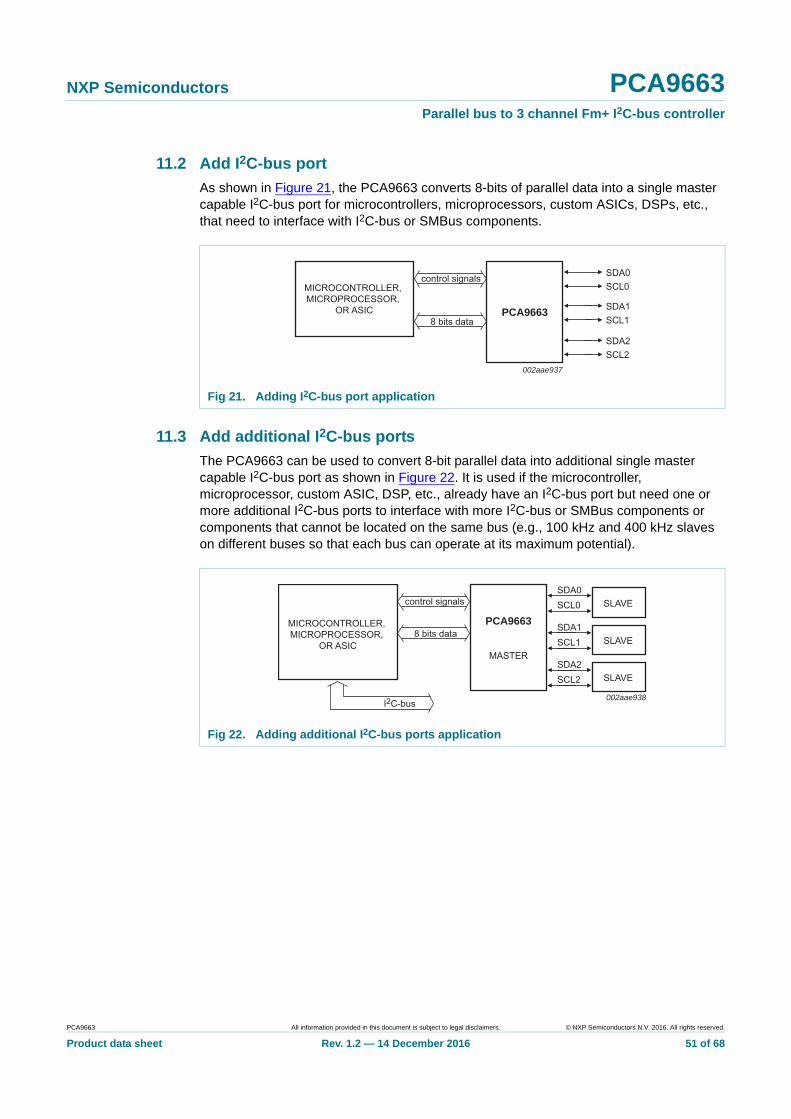
NXP Semiconductors PCA9663Parallel bus to 3 channel Fm+ I2C-bus controller
11.2 Add I2C-bus port
As shown in Figure 21, the PCA9663 converts 8-bits of parallel data into a single master capable I2C-bus port for microcontrollers, microprocessors, custom ASICs, DSPs, etc., that need to interface with I2C-bus or SMBus components.
11.3 Add additional I2C-bus ports
The PCA9663 can be used to convert 8-bit parallel data into additional single master capable I2C-bus port as shown in Figure 22. It is used if the microcontroller, microprocessor, custom ASIC, DSP, etc., already have an I2C-bus port but need one or more additional I2C-bus ports to interface with more I2C-bus or SMBus components or components that cannot be located on the same bus (e.g., 100 kHz and 400 kHz slaves on different buses so that each bus can operate at its maximum potential).
Fig 21. Adding I2C-bus port application
MICROCONTROLLER, MICROPROCESSOR,
OR ASIC
control signals
8 bits dataPCA9663
SDA0SCL0
002aae937
SDA1SCL1
SDA2SCL2
Fig 22. Adding additional I2C-bus ports application
control signals
8 bits dataPCA9663
SDA0SCL0
002aae938
SLAVE
MICROCONTROLLER, MICROPROCESSOR,
OR ASIC
SDA1SCL1 SLAVE
SDA2SCL2 SLAVE
MASTER
I2C-bus
PCA9663 All information provided in this document is subject to legal disclaimers. © NXP Semiconductors N.V. 2016. All rights reserved.
Product data sheet Rev. 1.2 — 14 December 2016 51 of 68

NXP Semiconductors PCA9663Parallel bus to 3 channel Fm+ I2C-bus controller
12. Limiting values
[1] 5.5 V steady state voltage tolerance on inputs and outputs is valid only when the supply voltage is present. 4.6 V steady state voltage tolerance on inputs and outputs when no supply voltage is present.
13. Static characteristics
Table 35. Limiting valuesIn accordance with the Absolute Maximum Rating System (IEC 60134).
Symbol Parameter Conditions Min Max Unit
VDD supply voltage 0.3 +4.6 V
VDD(IO) input/output supply voltage power supply reference for I2C-bus I/O pins
0.3 +7.0 V
VI input voltage parallel bus interface 0.3 +4.6 V
I2C-bus pins [1] 0.3 +7.0 V
II input current any input 10 +10 mA
IO output current any output 10 +10 mA
IOSH HIGH-level short-circuit output current I/O D0 to D7 - 106 mA
IOSL LOW-level short-circuit output current I/O D0 to D7 - 110 mA
Ptot total power dissipation - 300 mW
P/out power dissipation per output - 50 mW
Tstg storage temperature 65 +150 C
Tamb ambient temperature operating 40 +85 C
Table 36. Static characteristicsVDD = 3.0 V to 3.6 V; Tamb = 40 C to +85 C; unless otherwise specified.
Symbol Parameter Conditions Min Typ Max Unit
Supply
VDD supply voltage monotonic supply during power-up and power-down with a ramp time (tramp): 5 s < tr < 20 ms (5 % VDD(min) to 95 % VDD(min))
3.0 - 3.6 V
VDD(PLL) phase-locked loop supply voltage
power supply for PLL bias circuit 3.0 - 3.6 V
VDD(IO) input/output supply voltage power supply reference for I2C-bus I/O pins
3.0 - 5.5 V
IDD supply current operating mode; no load - 15 25 mA
IDD(IO) input/output supply current VDD(IO) = 5.5 V; VDD = 3.6 V; I/O not switching
- - 1 mA
VPOR power-on reset voltage LOW to HIGH - 2.75 - V
HIGH to LOW - 2.60 - V
PCA9663 All information provided in this document is subject to legal disclaimers. © NXP Semiconductors N.V. 2016. All rights reserved.
Product data sheet Rev. 1.2 — 14 December 2016 52 of 68

NXP Semiconductors PCA9663Parallel bus to 3 channel Fm+ I2C-bus controller
[1] 5.5 V steady state voltage tolerance on inputs and outputs is valid only when the supply voltage is present. 4.6 V steady state voltage tolerance on inputs and outputs when no supply voltage is present.
Inputs WR, RD, A0 to A7, CE, TRIG
VIL LOW-level input voltage 0 - 0.3VDD V
VIH HIGH-level input voltage [1] 0.7VDD - 3.6 V
Vhys hysteresis voltage 0.1VDD - - V
IL leakage current input; VI = 0 V or 3.6 V 1 - +1 A
Ci input capacitance VI = VSS or VDD - 2.0 4.5 pF
Input RESET
VIL LOW-level input voltage 0 - 0.3VDD V
VIH HIGH-level input voltage [1] 0.7VDD - 3.6 V
Vhys hysteresis voltage 0.1VDD - - V
IL leakage current input; VI = 0 V or 3.6 V 1 - +75 A
Ci input capacitance VI = VSS or VDD - 2.0 4.5 pF
Inputs/outputs D0 to D7
VIL LOW-level input voltage 0 - 0.3VDD V
VIH HIGH-level input voltage 0.7VDD - 3.6 V
IOH HIGH-level output current VOH = VDD(IO) 0.4 V 3.2 - - mA
IOL LOW-level output current VOL = 0.4 V 2.0 - - mA
IL leakage current input; VI = 0 V or 5.5 V 1 - +1 A
Cio input/output capacitance VI = VSS or VDD - 2.8 5 pF
SDAn and SCLn
VIL LOW-level input voltage 0 - 0.3VDD(IO) V
VIH HIGH-level input voltage [1] 0.7VDD(IO) - 5.5 V
IL leakage current input/output; VI = 0 V or 3.6 V 75 - +1 A
input/output; VI = 5.5 V 75 - +1 A
IOL LOW-level output current VOL = 0.4 V 30 - - mA
Cio input/output capacitance VI = VSS or VDD(IO) - 5.6 7 pF
Outputs INT
IOL LOW-level output current VOL = 0.4 V 6.0 - - mA
IL leakage current VO = 0 V or 3.6 V 1 - +75 A
Co output capacitance VI = VSS or VDD - 3.8 5.5 pF
Table 36. Static characteristics …continuedVDD = 3.0 V to 3.6 V; Tamb = 40 C to +85 C; unless otherwise specified.
Symbol Parameter Conditions Min Typ Max Unit
PCA9663 All information provided in this document is subject to legal disclaimers. © NXP Semiconductors N.V. 2016. All rights reserved.
Product data sheet Rev. 1.2 — 14 December 2016 53 of 68

NXP Semiconductors PCA9663Parallel bus to 3 channel Fm+ I2C-bus controller
14. Dynamic characteristics
[1] Parameters are valid over specified temperature and voltage range.
[2] All voltage measurements are referenced to ground (VSS). For testing, all inputs swing between 0 V and 3.0 V with a transition time of 5 ns maximum. All time measurements are referenced at input voltages of 1.5 V and output voltages shown in Figure 23 and Figure 25.
[3] Test conditions for outputs: CL = 50 pF; RL = 500 , except open-drain outputs.
Test conditions for open-drain outputs: CL = 50 pF; RL = 1 k pull-up to VDD.
[4] Resetting the device while actively communicating on the bus may cause glitches or an errant STOP condition.
[5] Upon reset, the full delay will be the sum of trst and the RC time constant of the SDA and SCL bus.
Table 37. Dynamic characteristics (3.3 volt)[1][2][3]
VDD = 3.3 V 0.3 V; Tamb = 40 C to +85 C; unless otherwise specified.
Symbol Parameter Conditions Min Typ Max Unit
Initialization timing
tinit(po) power-on initialization time VDD = 3.0 V - - 650 s
tinit initialization time channel initialization time from Channel Software Reset
- - 70 s
controller initialization time from POR, RESET, or Global Software Reset inactive
- - 650 s
RESET timing
tw(rst) reset pulse width 4 - - s
trst reset time [4][5] 1.5 - - s
INT timing
tas(int) interrupt assert time - - 500 ns
tdas(int) interrupt de-assert time - - 100 ns
TRIG timing
tw(trig) trigger pulse width HIGH or LOW 100 - - ns
Bus timing (see Figure 23 and Figure 25)
tsu(A) address set-up time to RD, WR LOW 0 - - ns
th(A) address hold time from RD, WR LOW 14 - - ns
tsu(CE_N) CE set-up time to RD, WR LOW 0 - - ns
th(CE_N) CE hold time from RD, WR LOW 0 - - ns
tw(RDL) RD LOW pulse width 40 - - ns
tw(WRL) WR LOW pulse width 40 - - ns
td(DV) data valid delay time after RD and CE LOW - - 45 ns
td(QZ) data output float delay time after RD or CE HIGH - - 7 ns
tsu(Q) data output set-up time before WR HIGH 5 - - ns
th(Q) data output hold time after WR HIGH 2 - - ns
tw(RDH) RD HIGH pulse width 40 - - ns
tw(WRH) WR HIGH pulse width 40 - - ns
PCA9663 All information provided in this document is subject to legal disclaimers. © NXP Semiconductors N.V. 2016. All rights reserved.
Product data sheet Rev. 1.2 — 14 December 2016 54 of 68

NXP Semiconductors PCA9663Parallel bus to 3 channel Fm+ I2C-bus controller
Fig 23. Bus timing (read cycle)
Fig 24. Parallel bus timing (write cycle)
A0 to A7
CE
RD
D0 to D7(read)
002aaf458
tsu(A)th(A)
tsu(CE_N) th(CE_N)tw(RDL) tw(RDH)
float floatnot valid valid
td(DV)td(QZ)
A0 to A7
CE
002aaf459
tsu(A)th(A)
tsu(CE_N) th(CE_N)
WR
valid
tw(WRH)
D0 to D7(write)
tsu(Q)th(Q)
tw(WRL)
PCA9663 All information provided in this document is subject to legal disclaimers. © NXP Semiconductors N.V. 2016. All rights reserved.
Product data sheet Rev. 1.2 — 14 December 2016 55 of 68

NXP Semiconductors PCA9663Parallel bus to 3 channel Fm+ I2C-bus controller
VM = 1.5 V
VX = VOL + 0.2 V
VY = VOH 0.2 V
VOL and VOH are typical output voltage drops that occur with the output load.
Fig 25. Data timing
002aaf172
td(QLZ)
td(QHZ)
outputsfloating
outputsenabled
outputsenabled
Dn outputLOW-to-floatfloat-to-LOW
Dn outputHIGH-to-floatfloat-to-HIGH
RD, CE input
VI
VOL
VOH
VDD
VM
VM
VX
VY
VM
VSS
VSS
td(QZL)
td(QZH)
VM
PCA9663 All information provided in this document is subject to legal disclaimers. © NXP Semiconductors N.V. 2016. All rights reserved.
Product data sheet Rev. 1.2 — 14 December 2016 56 of 68
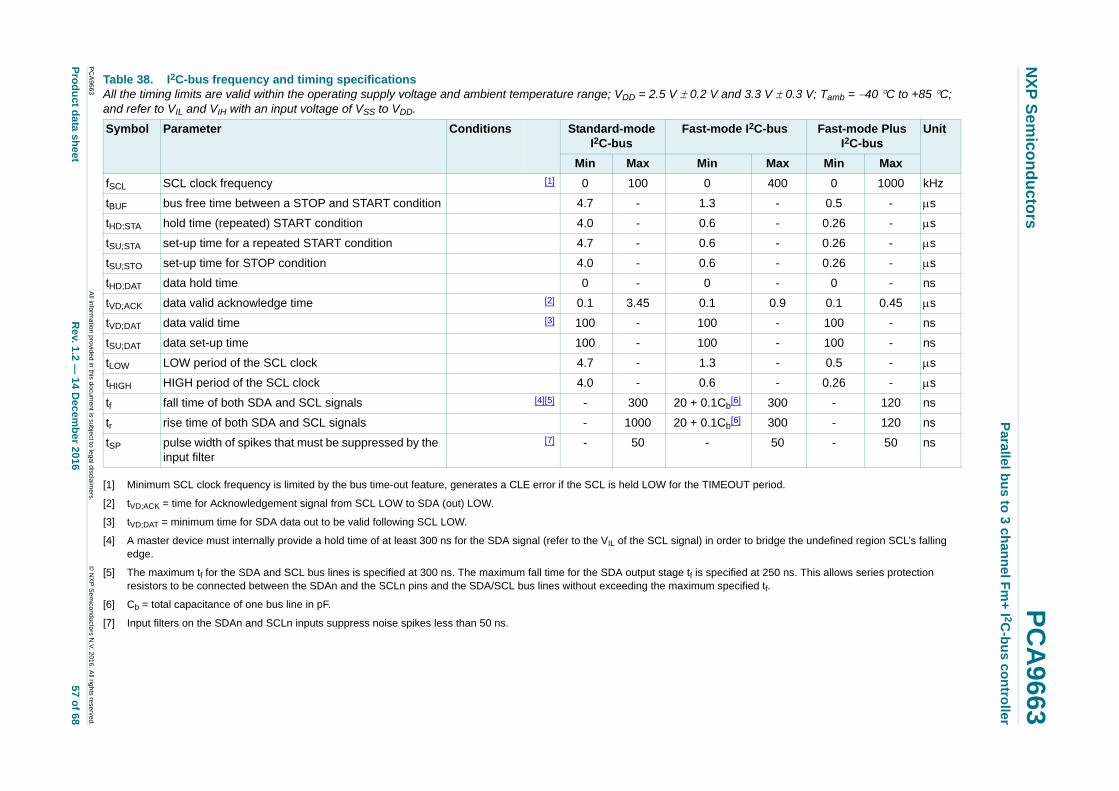
xxxxxxxxxxxxxxxxxxxxx xxxxxxxxxxxxxxxxxxxxxxxxxx xxxxxxx x x x xxxxxxxxxxxxxxxxxxxxxxxxxxxxxx xxxxxxxxxxxxxxxxxxx xx xx xxxxx xxxxxxxxxxxxxxxxxxxxxxxxxxx xxxxxxxxxxxxxxxxxxx xxxxxx xxxxxxxxxxxxxxxxxxxxxxxxxxxxxxxxxxx xxxxxxxxxxxx x x xxxxxxxxxxxxxxxxxxxxx xxxxxxxxxxxxxxxxxxxxxxxxxxxxxx xxxxx xxxxxxxxxxxxxxxxxxxxxxxxxxxxxxxxxxxxxxxxxxxxxxxxxx xxxxxxxx xxxxxxxxxxxxxxxxxxxxxxxxx xxxxxxxxxxxxxxxxxxxx xxx
PC
A966
3
Pro
du
ct data sh
NX
P S
emico
nd
ucto
rsP
CA
9663P
arallel bu
s to 3 ch
ann
el Fm
+ I 2C
-bu
s c
on
troller
T period.
r to bridge the undefined region SCL’s falling
d at 250 ns. This allows series protection ified tf.
Table 38. I2C-bus frequency and timing specificationsAll the timing limits are valid within the operating supply voltage and ambient temperature range; VDD = 2.5 V 0.2 V and 3.3 V 0.3 V; Tamb = 40 C to +85 C; and refer to VIL and VIH with an input voltage of VSS to VDD.
Symbol Parameter Conditions Standard-mode 2
Fast-mode I2C-bus Fast-mode Plus I2C-bus
Unit
Max Min Max
400 0 1000 kHz
- 0.5 - s
- 0.26 - s
- 0.26 - s
- 0.26 - s
- 0 - ns
0.9 0.1 0.45 s
- 100 - ns
- 100 - ns
- 0.5 - s
- 0.26 - s] 300 - 120 ns] 300 - 120 ns
50 - 50 ns
All inform
ation provided
in this docum
ent is subject to leg
al disclaim
ers.©
NX
P S
em
iconductors N
.V. 2016. A
ll rights reserved.
eetR
ev. 1.2 — 14 D
ecemb
er 2016 57 o
f 68
[1] Minimum SCL clock frequency is limited by the bus time-out feature, generates a CLE error if the SCL is held LOW for the TIMEOU
[2] tVD;ACK = time for Acknowledgement signal from SCL LOW to SDA (out) LOW.
[3] tVD;DAT = minimum time for SDA data out to be valid following SCL LOW.
[4] A master device must internally provide a hold time of at least 300 ns for the SDA signal (refer to the VIL of the SCL signal) in ordeedge.
[5] The maximum tf for the SDA and SCL bus lines is specified at 300 ns. The maximum fall time for the SDA output stage tf is specifieresistors to be connected between the SDAn and the SCLn pins and the SDA/SCL bus lines without exceeding the maximum spec
[6] Cb = total capacitance of one bus line in pF.
[7] Input filters on the SDAn and SCLn inputs suppress noise spikes less than 50 ns.
I C-bus
Min Max Min
fSCL SCL clock frequency [1] 0 100 0
tBUF bus free time between a STOP and START condition 4.7 - 1.3
tHD;STA hold time (repeated) START condition 4.0 - 0.6
tSU;STA set-up time for a repeated START condition 4.7 - 0.6
tSU;STO set-up time for STOP condition 4.0 - 0.6
tHD;DAT data hold time 0 - 0
tVD;ACK data valid acknowledge time [2] 0.1 3.45 0.1
tVD;DAT data valid time [3] 100 - 100
tSU;DAT data set-up time 100 - 100
tLOW LOW period of the SCL clock 4.7 - 1.3
tHIGH HIGH period of the SCL clock 4.0 - 0.6
tf fall time of both SDA and SCL signals [4][5] - 300 20 + 0.1Cb[6
tr rise time of both SDA and SCL signals - 1000 20 + 0.1Cb[6
tSP pulse width of spikes that must be suppressed by the input filter
[7] - 50 -

NXP Semiconductors PCA9663Parallel bus to 3 channel Fm+ I2C-bus controller
Fig 26. Definition of timing on the I2C-bus
DA
SCL
002aab27
tf
S Sr P StHD;STA
tLOW
tr
tSU;DAT
tf
tHD;DAT
tHIGH tSU;STA
tHD;STA tSP
tSU;STO
tr
tBUF
0.7 × VDD0.3 × VDD
0.7 × VDD0.3 × VDD
Rise and fall times refer to VIL and VIH.
Fig 27. I2C-bus timing diagram
SCL
SDA
tHD;STA tSU;DAT tHD;DAT
tftBUF
tSU;STA tLOW tHIGH
tVD;ACK
002aac6
otocolSTART
condition(S)
bit 7MSB bit 6 bit n bit 0 acknowledge
(A)
1/fSCL
tr
tVD;DAT tSU;STO
STOPcondition
(P)
0.7 × V0.3 × V
0.7 × V0.3 × V
PCA9663 All information provided in this document is subject to legal disclaimers. © NXP Semiconductors N.V. 2016. All rights reserved.
Product data sheet Rev. 1.2 — 14 December 2016 58 of 68

NXP Semiconductors PCA9663Parallel bus to 3 channel Fm+ I2C-bus controller
15. Test information
Test data are given in Table 39.
RL = load resistance.
CL = load capacitance includes jig and probe capacitance.
RT = termination resistance should be equal to the output impedance ZO of the pulse generators.
Fig 28. Test circuitry for switching times
Table 39. Test data
Test Conditions Load S1
CL RL
td(DV), td(QZ) Dn outputs active LOW 50 pF 500 VDD 2
Dn outputs active HIGH 50 pF 500 open
Test data are given in Table 40.
RL = load resistance.
CL = load capacitance includes jig and probe capacitance.
RT = termination resistance should be equal to the output impedance ZO of the pulse generators.
Fig 29. Test circuitry for open-drain switching times
Table 40. Test data INT pin
Test Load S1
CL RL
tas(int) 50 pF 1 k VDD
tdas(int) 50 pF 1 k VDD
PULSEGENERATOR
VO
CL50 pF
RL500 Ω
002aac694
RT
VI
VDD
DUT
RL500 Ω
VDD × 2openVSS
PULSEGENERATOR
VO
CL50 pF
RL1 kΩ
002aac695
RT
VI
VDD
DUT
VDDopenVSS
PCA9663 All information provided in this document is subject to legal disclaimers. © NXP Semiconductors N.V. 2016. All rights reserved.
Product data sheet Rev. 1.2 — 14 December 2016 59 of 68

NXP Semiconductors PCA9663Parallel bus to 3 channel Fm+ I2C-bus controller
16. Package outline
Fig 30. Package outline SOT313-2 (LQFP48)
UNITA
max. A1 A2 A3 bp c E(1) e HE L Lp Zywv θ
REFERENCESOUTLINEVERSION
EUROPEANPROJECTION ISSUE DATE
IEC JEDEC JEITA
mm 1.6 0.200.05
1.451.35
0.250.270.17
0.180.12
7.16.9 0.5
9.158.85
0.950.55
70
o
o0.12 0.10.21
DIMENSIONS (mm are the original dimensions)
Note
1. Plastic or metal protrusions of 0.25 mm maximum per side are not included.
0.750.45
SOT313-2 MS-026136E0500-01-1903-02-25
D(1) (1)(1)
7.16.9
HD
9.158.85
EZ
0.950.55
D
bp
e
E
B
12
DH
bp
EH
v M B
D
ZD
A
ZE
e
v M A
1
48
37
36 25
24
13
θ
A1A
Lp
detail X
L
(A )3A2
X
y
c
w M
w M
0 2.5 5 mm
scale
pin 1 index
LQFP48: plastic low profile quad flat package; 48 leads; body 7 x 7 x 1.4 mm SOT313-2
PCA9663 All information provided in this document is subject to legal disclaimers. © NXP Semiconductors N.V. 2016. All rights reserved.
Product data sheet Rev. 1.2 — 14 December 2016 60 of 68

NXP Semiconductors PCA9663Parallel bus to 3 channel Fm+ I2C-bus controller
17. Handling information
All input and output pins are protected against ElectroStatic Discharge (ESD) under normal handling. When handling ensure that the appropriate precautions are taken as described in JESD625-A or equivalent standards.
18. Soldering of SMD packages
This text provides a very brief insight into a complex technology. A more in-depth account of soldering ICs can be found in Application Note AN10365 “Surface mount reflow soldering description”.
18.1 Introduction to soldering
Soldering is one of the most common methods through which packages are attached to Printed Circuit Boards (PCBs), to form electrical circuits. The soldered joint provides both the mechanical and the electrical connection. There is no single soldering method that is ideal for all IC packages. Wave soldering is often preferred when through-hole and Surface Mount Devices (SMDs) are mixed on one printed wiring board; however, it is not suitable for fine pitch SMDs. Reflow soldering is ideal for the small pitches and high densities that come with increased miniaturization.
18.2 Wave and reflow soldering
Wave soldering is a joining technology in which the joints are made by solder coming from a standing wave of liquid solder. The wave soldering process is suitable for the following:
• Through-hole components
• Leaded or leadless SMDs, which are glued to the surface of the printed circuit board
Not all SMDs can be wave soldered. Packages with solder balls, and some leadless packages which have solder lands underneath the body, cannot be wave soldered. Also, leaded SMDs with leads having a pitch smaller than ~0.6 mm cannot be wave soldered, due to an increased probability of bridging.
The reflow soldering process involves applying solder paste to a board, followed by component placement and exposure to a temperature profile. Leaded packages, packages with solder balls, and leadless packages are all reflow solderable.
Key characteristics in both wave and reflow soldering are:
• Board specifications, including the board finish, solder masks and vias
• Package footprints, including solder thieves and orientation
• The moisture sensitivity level of the packages
• Package placement
• Inspection and repair
• Lead-free soldering versus SnPb soldering
18.3 Wave soldering
Key characteristics in wave soldering are:
PCA9663 All information provided in this document is subject to legal disclaimers. © NXP Semiconductors N.V. 2016. All rights reserved.
Product data sheet Rev. 1.2 — 14 December 2016 61 of 68

NXP Semiconductors PCA9663Parallel bus to 3 channel Fm+ I2C-bus controller
• Process issues, such as application of adhesive and flux, clinching of leads, board transport, the solder wave parameters, and the time during which components are exposed to the wave
• Solder bath specifications, including temperature and impurities
18.4 Reflow soldering
Key characteristics in reflow soldering are:
• Lead-free versus SnPb soldering; note that a lead-free reflow process usually leads to higher minimum peak temperatures (see Figure 31) than a SnPb process, thus reducing the process window
• Solder paste printing issues including smearing, release, and adjusting the process window for a mix of large and small components on one board
• Reflow temperature profile; this profile includes preheat, reflow (in which the board is heated to the peak temperature) and cooling down. It is imperative that the peak temperature is high enough for the solder to make reliable solder joints (a solder paste characteristic). In addition, the peak temperature must be low enough that the packages and/or boards are not damaged. The peak temperature of the package depends on package thickness and volume and is classified in accordance with Table 41 and 42
Moisture sensitivity precautions, as indicated on the packing, must be respected at all times.
Studies have shown that small packages reach higher temperatures during reflow soldering, see Figure 31.
Table 41. SnPb eutectic process (from J-STD-020D)
Package thickness (mm) Package reflow temperature (C)
Volume (mm3)
< 350 350
< 2.5 235 220
2.5 220 220
Table 42. Lead-free process (from J-STD-020D)
Package thickness (mm) Package reflow temperature (C)
Volume (mm3)
< 350 350 to 2000 > 2000
< 1.6 260 260 260
1.6 to 2.5 260 250 245
> 2.5 250 245 245
PCA9663 All information provided in this document is subject to legal disclaimers. © NXP Semiconductors N.V. 2016. All rights reserved.
Product data sheet Rev. 1.2 — 14 December 2016 62 of 68

NXP Semiconductors PCA9663Parallel bus to 3 channel Fm+ I2C-bus controller
For further information on temperature profiles, refer to Application Note AN10365 “Surface mount reflow soldering description”.
19. Abbreviations
MSL: Moisture Sensitivity Level
Fig 31. Temperature profiles for large and small components
001aac844
temperature
time
minimum peak temperature= minimum soldering temperature
maximum peak temperature= MSL limit, damage level
peak temperature
Table 43. Abbreviations
Acronym Description
ASIC Application Specific Integrated Circuit
CPU Central Processing Unit
CDM Charged-Device Model
DSP Digital Signal Processor
ESD ElectroStatic Discharge
Fm+ Fast-mode Plus
HBM Human Body Model
I2C-bus Inter-Integrated Circuit bus
I/O Input/Output
LED Light Emitting Diode
PLL Phase-Locked Loop
SMBus System Management Bus
PCA9663 All information provided in this document is subject to legal disclaimers. © NXP Semiconductors N.V. 2016. All rights reserved.
Product data sheet Rev. 1.2 — 14 December 2016 63 of 68
NXP Semiconductors PCA9663Parallel bus to 3 channel Fm+ I2C-bus controller
20. Revision history
Table 44. Revision history
Document ID Release date Data sheet status Change notice Supersedes
PCA9663 v.1.2 20161214 Product data sheet - PCA9663 v.1.1
Modifications: • Table 3 “Pin description”: Corrected pin type for pins 21, 22, 25, and 26 from “O” to “I/O”
PCA9663 v.1.1 20150622 Product data sheet - PCA9663 v.1
Modifications: • Added Section 4.1 “Ordering options”
• Table 22: Added “Channel 1 = DBh and Channel 2 = EBh” to address
• Table 23: Added “Channel 1 = DCh and Channel 2 = ECh” to address
• Table 28: Added “Channel 1 = DEh and Channel 2 = EEh” to address
PCA9663 v.1 20110606 Product data sheet - -
PCA9663 All information provided in this document is subject to legal disclaimers. © NXP Semiconductors N.V. 2016. All rights reserved.
Product data sheet Rev. 1.2 — 14 December 2016 64 of 68

NXP Semiconductors PCA9663Parallel bus to 3 channel Fm+ I2C-bus controller
21. Legal information
21.1 Data sheet status
[1] Please consult the most recently issued document before initiating or completing a design.
[2] The term ‘short data sheet’ is explained in section “Definitions”.
[3] The product status of device(s) described in this document may have changed since this document was published and may differ in case of multiple devices. The latest product status information is available on the Internet at URL http://www.nxp.com.
21.2 Definitions
Draft — The document is a draft version only. The content is still under internal review and subject to formal approval, which may result in modifications or additions. NXP Semiconductors does not give any representations or warranties as to the accuracy or completeness of information included herein and shall have no liability for the consequences of use of such information.
Short data sheet — A short data sheet is an extract from a full data sheet with the same product type number(s) and title. A short data sheet is intended for quick reference only and should not be relied upon to contain detailed and full information. For detailed and full information see the relevant full data sheet, which is available on request via the local NXP Semiconductors sales office. In case of any inconsistency or conflict with the short data sheet, the full data sheet shall prevail.
Product specification — The information and data provided in a Product data sheet shall define the specification of the product as agreed between NXP Semiconductors and its customer, unless NXP Semiconductors and customer have explicitly agreed otherwise in writing. In no event however, shall an agreement be valid in which the NXP Semiconductors product is deemed to offer functions and qualities beyond those described in the Product data sheet.
21.3 Disclaimers
Limited warranty and liability — Information in this document is believed to be accurate and reliable. However, NXP Semiconductors does not give any representations or warranties, expressed or implied, as to the accuracy or completeness of such information and shall have no liability for the consequences of use of such information. NXP Semiconductors takes no responsibility for the content in this document if provided by an information source outside of NXP Semiconductors.
In no event shall NXP Semiconductors be liable for any indirect, incidental, punitive, special or consequential damages (including - without limitation - lost profits, lost savings, business interruption, costs related to the removal or replacement of any products or rework charges) whether or not such damages are based on tort (including negligence), warranty, breach of contract or any other legal theory.
Notwithstanding any damages that customer might incur for any reason whatsoever, NXP Semiconductors’ aggregate and cumulative liability towards customer for the products described herein shall be limited in accordance with the Terms and conditions of commercial sale of NXP Semiconductors.
Right to make changes — NXP Semiconductors reserves the right to make changes to information published in this document, including without limitation specifications and product descriptions, at any time and without notice. This document supersedes and replaces all information supplied prior to the publication hereof.
Suitability for use — NXP Semiconductors products are not designed, authorized or warranted to be suitable for use in life support, life-critical or safety-critical systems or equipment, nor in applications where failure or malfunction of an NXP Semiconductors product can reasonably be expected to result in personal injury, death or severe property or environmental damage. NXP Semiconductors and its suppliers accept no liability for inclusion and/or use of NXP Semiconductors products in such equipment or applications and therefore such inclusion and/or use is at the customer’s own risk.
Applications — Applications that are described herein for any of these products are for illustrative purposes only. NXP Semiconductors makes no representation or warranty that such applications will be suitable for the specified use without further testing or modification.
Customers are responsible for the design and operation of their applications and products using NXP Semiconductors products, and NXP Semiconductors accepts no liability for any assistance with applications or customer product design. It is customer’s sole responsibility to determine whether the NXP Semiconductors product is suitable and fit for the customer’s applications and products planned, as well as for the planned application and use of customer’s third party customer(s). Customers should provide appropriate design and operating safeguards to minimize the risks associated with their applications and products.
NXP Semiconductors does not accept any liability related to any default, damage, costs or problem which is based on any weakness or default in the customer’s applications or products, or the application or use by customer’s third party customer(s). Customer is responsible for doing all necessary testing for the customer’s applications and products using NXP Semiconductors products in order to avoid a default of the applications and the products or of the application or use by customer’s third party customer(s). NXP does not accept any liability in this respect.
Limiting values — Stress above one or more limiting values (as defined in the Absolute Maximum Ratings System of IEC 60134) will cause permanent damage to the device. Limiting values are stress ratings only and (proper) operation of the device at these or any other conditions above those given in the Recommended operating conditions section (if present) or the Characteristics sections of this document is not warranted. Constant or repeated exposure to limiting values will permanently and irreversibly affect the quality and reliability of the device.
Terms and conditions of commercial sale — NXP Semiconductors products are sold subject to the general terms and conditions of commercial sale, as published at http://www.nxp.com/profile/terms, unless otherwise agreed in a valid written individual agreement. In case an individual agreement is concluded only the terms and conditions of the respective agreement shall apply. NXP Semiconductors hereby expressly objects to applying the customer’s general terms and conditions with regard to the purchase of NXP Semiconductors products by customer.
No offer to sell or license — Nothing in this document may be interpreted or construed as an offer to sell products that is open for acceptance or the grant, conveyance or implication of any license under any copyrights, patents or other industrial or intellectual property rights.
Document status[1][2] Product status[3] Definition
Objective [short] data sheet Development This document contains data from the objective specification for product development.
Preliminary [short] data sheet Qualification This document contains data from the preliminary specification.
Product [short] data sheet Production This document contains the product specification.
PCA9663 All information provided in this document is subject to legal disclaimers. © NXP Semiconductors N.V. 2016. All rights reserved.
Product data sheet Rev. 1.2 — 14 December 2016 65 of 68

NXP Semiconductors PCA9663Parallel bus to 3 channel Fm+ I2C-bus controller
Export control — This document as well as the item(s) described herein may be subject to export control regulations. Export might require a prior authorization from competent authorities.
Non-automotive qualified products — Unless this data sheet expressly states that this specific NXP Semiconductors product is automotive qualified, the product is not suitable for automotive use. It is neither qualified nor tested in accordance with automotive testing or application requirements. NXP Semiconductors accepts no liability for inclusion and/or use of non-automotive qualified products in automotive equipment or applications.
In the event that customer uses the product for design-in and use in automotive applications to automotive specifications and standards, customer (a) shall use the product without NXP Semiconductors’ warranty of the product for such automotive applications, use and specifications, and (b)
whenever customer uses the product for automotive applications beyond NXP Semiconductors’ specifications such use shall be solely at customer’s own risk, and (c) customer fully indemnifies NXP Semiconductors for any liability, damages or failed product claims resulting from customer design and use of the product for automotive applications beyond NXP Semiconductors’ standard warranty and NXP Semiconductors’ product specifications.
21.4 TrademarksNotice: All referenced brands, product names, service names and trademarks are the property of their respective owners.
I2C-bus — logo is a trademark of NXP B.V.
22. Contact information
For more information, please visit: http://www.nxp.com
For sales office addresses, please send an email to: [email protected]
PCA9663 All information provided in this document is subject to legal disclaimers. © NXP Semiconductors N.V. 2016. All rights reserved.
Product data sheet Rev. 1.2 — 14 December 2016 66 of 68

NXP Semiconductors PCA9663Parallel bus to 3 channel Fm+ I2C-bus controller
23. Contents
1 General description . . . . . . . . . . . . . . . . . . . . . . 1
2 Features and benefits . . . . . . . . . . . . . . . . . . . . 1
3 Applications . . . . . . . . . . . . . . . . . . . . . . . . . . . . 2
4 Ordering information. . . . . . . . . . . . . . . . . . . . . 24.1 Ordering options . . . . . . . . . . . . . . . . . . . . . . . . 2
5 Block diagram . . . . . . . . . . . . . . . . . . . . . . . . . . 3
6 Pinning information. . . . . . . . . . . . . . . . . . . . . . 46.1 Pinning . . . . . . . . . . . . . . . . . . . . . . . . . . . . . . . 46.2 Pin description . . . . . . . . . . . . . . . . . . . . . . . . . 4
7 Functional description . . . . . . . . . . . . . . . . . . . 67.1 General . . . . . . . . . . . . . . . . . . . . . . . . . . . . . . . 67.2 Internal oscillator and PLL . . . . . . . . . . . . . . . . 67.3 Buffer description . . . . . . . . . . . . . . . . . . . . . . . 67.3.1 Buffer management assumptions . . . . . . . . . . . 77.3.2 Buffer sizes . . . . . . . . . . . . . . . . . . . . . . . . . . . . 77.4 Error reporting and handling. . . . . . . . . . . . . . . 87.5 Registers . . . . . . . . . . . . . . . . . . . . . . . . . . . . . 87.5.1 Channel registers . . . . . . . . . . . . . . . . . . . . . . 137.5.1.1 STATUS0_[n], STATUS1_[n], STATUS2_[n] —
Transaction status registers . . . . . . . . . . . . . . 137.5.1.2 CONTROL — Control register . . . . . . . . . . . . 147.5.1.3 CHSTATUS — Channel status register . . . . . 177.5.1.4 INTMSK — Interrupt mask register. . . . . . . . . 197.5.1.5 SLATABLE — Slave address table register . . 207.5.1.6 TRANCONFIG — Transaction configuration
register . . . . . . . . . . . . . . . . . . . . . . . . . . . . . . 217.5.1.7 DATA — I2C-bus Data register . . . . . . . . . . . . 217.5.1.8 TRANSEL — Transaction data buffer select
register . . . . . . . . . . . . . . . . . . . . . . . . . . . . . . 227.5.1.9 TRANOFS — Transaction data buffer byte select
register . . . . . . . . . . . . . . . . . . . . . . . . . . . . . . 237.5.1.10 BYTECOUNT — Transmitted and received byte
count register . . . . . . . . . . . . . . . . . . . . . . . . . 237.5.1.11 FRAMECNT — Frame count register . . . . . . . 237.5.1.12 REFRATE — Refresh rate register. . . . . . . . . 247.5.1.13 SCLL, SCLH — Clock rate registers. . . . . . . . 247.5.1.14 MODE — I2C-bus mode register . . . . . . . . . . 277.5.1.15 TIMEOUT — Time-out register. . . . . . . . . . . . 287.5.1.16 PRESET — I2C-bus channel parallel software
reset register. . . . . . . . . . . . . . . . . . . . . . . . . . 297.5.2 Global registers . . . . . . . . . . . . . . . . . . . . . . . 297.5.2.1 CTRLSTATUS — Controller status register . . 297.5.2.2 CTRLINTMSK — Control Interrupt mask
register . . . . . . . . . . . . . . . . . . . . . . . . . . . . . . 317.5.2.3 DEVICE_ID — Device ID . . . . . . . . . . . . . . . . 327.5.2.4 CTRLPRESET — Parallel software reset
register . . . . . . . . . . . . . . . . . . . . . . . . . . . . . . 33
7.5.2.5 CTRLRDY — Controller ready register . . . . . 33
8 PCA9663 operation . . . . . . . . . . . . . . . . . . . . . 358.1 Sequence execution . . . . . . . . . . . . . . . . . . . 368.2 Read transactions . . . . . . . . . . . . . . . . . . . . . 408.3 Stopping a sequence . . . . . . . . . . . . . . . . . . . 408.4 Looping a sequence. . . . . . . . . . . . . . . . . . . . 408.4.1 Looping with REFRATE control . . . . . . . . . . . 418.4.2 Looping with Trigger control. . . . . . . . . . . . . . 418.5 Bus errors . . . . . . . . . . . . . . . . . . . . . . . . . . . 428.5.1 I2C-bus obstructed by a LOW level on SDA
(DAE) . . . . . . . . . . . . . . . . . . . . . . . . . . . . . . . 428.5.2 I2C-bus obstructed by a LOW level on SCL
(CLE) . . . . . . . . . . . . . . . . . . . . . . . . . . . . . . . 438.5.3 Illegal START or STOP (SSE) . . . . . . . . . . . . 438.6 Power-on reset. . . . . . . . . . . . . . . . . . . . . . . . 448.7 Global reset . . . . . . . . . . . . . . . . . . . . . . . . . . 448.8 Channel reset. . . . . . . . . . . . . . . . . . . . . . . . . 458.9 I2C-bus timing diagrams. . . . . . . . . . . . . . . . . 46
9 Characteristics of the I2C-bus . . . . . . . . . . . . 479.1 Bit transfer . . . . . . . . . . . . . . . . . . . . . . . . . . . 479.1.1 START and STOP conditions. . . . . . . . . . . . . 479.2 System configuration . . . . . . . . . . . . . . . . . . . 479.3 Acknowledge . . . . . . . . . . . . . . . . . . . . . . . . . 48
10 JTAG port . . . . . . . . . . . . . . . . . . . . . . . . . . . . . 49
11 Application design-in information. . . . . . . . . 5011.1 Specific applications. . . . . . . . . . . . . . . . . . . . 5011.2 Add I2C-bus port . . . . . . . . . . . . . . . . . . . . . . 5111.3 Add additional I2C-bus ports . . . . . . . . . . . . . 51
12 Limiting values . . . . . . . . . . . . . . . . . . . . . . . . 52
13 Static characteristics . . . . . . . . . . . . . . . . . . . 52
14 Dynamic characteristics. . . . . . . . . . . . . . . . . 54
15 Test information . . . . . . . . . . . . . . . . . . . . . . . 59
16 Package outline. . . . . . . . . . . . . . . . . . . . . . . . 60
17 Handling information . . . . . . . . . . . . . . . . . . . 61
18 Soldering of SMD packages. . . . . . . . . . . . . . 6118.1 Introduction to soldering. . . . . . . . . . . . . . . . . 6118.2 Wave and reflow soldering. . . . . . . . . . . . . . . 6118.3 Wave soldering . . . . . . . . . . . . . . . . . . . . . . . 6118.4 Reflow soldering . . . . . . . . . . . . . . . . . . . . . . 62
19 Abbreviations . . . . . . . . . . . . . . . . . . . . . . . . . 63
20 Revision history . . . . . . . . . . . . . . . . . . . . . . . 64
21 Legal information . . . . . . . . . . . . . . . . . . . . . . 6521.1 Data sheet status . . . . . . . . . . . . . . . . . . . . . . 6521.2 Definitions . . . . . . . . . . . . . . . . . . . . . . . . . . . 6521.3 Disclaimers . . . . . . . . . . . . . . . . . . . . . . . . . . 65
PCA9663 All information provided in this document is subject to legal disclaimers. © NXP Semiconductors N.V. 2016. All rights reserved.
Product data sheet Rev. 1.2 — 14 December 2016 67 of 68
continued >>

NXP Semiconductors PCA9663Parallel bus to 3 channel Fm+ I2C-bus controller
21.4 Trademarks. . . . . . . . . . . . . . . . . . . . . . . . . . . 66
22 Contact information. . . . . . . . . . . . . . . . . . . . . 66
23 Contents . . . . . . . . . . . . . . . . . . . . . . . . . . . . . . 67
© NXP Semiconductors N.V. 2016. All rights reserved.
For more information, please visit: http://www.nxp.comFor sales office addresses, please send an email to: [email protected]
Date of release: 14 December 2016
Document identifier: PCA9663
Please be aware that important notices concerning this document and the product(s)described herein, have been included in section ‘Legal information’.