Embed Size (px)
Citation preview

Patterned anvils for high pressure measurements at low temperatureOliver P. Welzel and F. Malte Grosche Citation: Review of Scientific Instruments 82, 033901 (2011); doi: 10.1063/1.3541793 View online: http://dx.doi.org/10.1063/1.3541793 View Table of Contents: http://scitation.aip.org/content/aip/journal/rsi/82/3?ver=pdfcov Published by the AIP Publishing Articles you may be interested in The low-frequency alternative-current magnetic susceptibility and electrical properties of Si(100)/Fe40Pd40B20(XÅ)/ZnO(500Å) and Si(100)/ZnO(500Å)/Fe40Pd40B20(YÅ) systems J. Appl. Phys. 113, 17B303 (2013); 10.1063/1.4794985 In situ electrical impedance spectroscopy under high pressure on diamond anvil cell Appl. Phys. Lett. 91, 092124 (2007); 10.1063/1.2778760 Integrated microcircuit on a diamond anvil for high-pressure electrical resistivity measurement Appl. Phys. Lett. 86, 064104 (2005); 10.1063/1.1863444 Moissanite (SiC) as windows and anvils for high-pressure infrared spectroscopy Rev. Sci. Instrum. 75, 5026 (2004); 10.1063/1.1808123 Effect of sintering temperature under high pressure on the superconductivity of MgB 2 Appl. Phys. Lett. 78, 4157 (2001); 10.1063/1.1382632
This article is copyrighted as indicated in the article. Reuse of AIP content is subject to the terms at: http://scitationnew.aip.org/termsconditions. Downloaded to IP:
129.105.215.146 On: Sat, 20 Dec 2014 11:17:48
REVIEW OF SCIENTIFIC INSTRUMENTS 82, 033901 (2011)
Patterned anvils for high pressure measurements at low temperatureOliver P. Welzela) and F. Malte GroscheCavendish Laboratory, Department of Physics, University of Cambridge, J. J. Thomson Avenue, CambridgeCB3 0HE, United Kingdom
(Received 15 October 2010; accepted 17 December 2010; published online 1 March 2011)
Multiprobe high pressure measurements require electrical leads in the sample chamber. Comparedto conventional wire-based techniques, metallic tracks patterned onto the anvil surface improve re-liability and ease of use, and enable novel and more demanding measurements under high pressure.We have developed new anvil designs based on sputter-deposited tracks on alumina and moissaniteanvils. These anvils allow convenient and reliable measurements of electrical transport properties orof the magnetic susceptibility under hydrostatic conditions, as demonstrated by test measurements onPb and Ca3Ru2O7. © 2011 American Institute of Physics. [doi:10.1063/1.3541793]
I. INTRODUCTION
High pressure is a key control parameter in the explo-ration of novel states in correlated electron systems. Vary-ing the lattice spacing through applied pressure effectivelyproduces an infinity of crystals from a single parent spec-imen, continuously, reversibly, and without introducing dis-order. Because transport properties reveal salient informationabout the electronic state of a system, measurements of theelectrical resistivity under high pressure have become an im-portant research tool in solid state physics.
Piston-cylinder pressure cells offer convenient and reli-able access to pressures of up to about 35 kbar for most pur-poses. In order to achieve pressures above 35 kbar, however,opposed anvil devices have to be used. Transport measure-ments in this type of pressure cell are fraught with difficul-ties, in particular when liquid pressure media are used. Theconventional methodology, which involves passing fine wiresacross an insulated, metallic gasket into the high pressure vol-ume, can fail in a number of ways: a wire may break, twowires may touch, or the insulation of the gasket may be com-promised. Any of these potential problems can invalidate themeasurement. Although a number of individuals have overthe years reported exciting results using the conventional ap-proach, the dexterity and skill required to employ this tech-nique slow down or even preclude the wider application ofpressure studies in novel materials. Moreover, implementingnew, more complex experimental probes in a high pressureenvironment requires a high level of reliability and accuracy,which is rarely achieved at present.
Leads could be passed into the high pressure space ofanvil pressure cells more reliably, if they were deposited asfilms on the anvil surface. This alternative approach has beenexplored successfully by a number of groups. When conduct-ing tracks were deposited on diamond surfaces and protectedby chemically vapor deposited diamond, resulting in so-calleddesigner diamonds, the results were particularly gratifying.1–3
More conventional approaches, in which tracks were laiddown on diamond anvils and were protected by by a sputter-deposited layer of alumina4 or by specially constructed
a)Electronic mail: [email protected].
compound gaskets,5 have also been reported. Usually, thesestudies did not make use of a liquid pressure medium.
Designer diamonds suffer from a number of difficulties:(i) the conducting films form carbides at the interface withthe diamond, which reduces the effective cross section of thefilm and results in large lead resistances,3 (ii) achieving highquality contacts between the conducting films and the sam-ple is difficult, given the small sample space in a typical de-signer diamond cell, and (iii) the technique is comparativelycostly, time consuming, and requires access to highly special-ized equipment and know how. The latter point, in particular,is likely to slow down the take up of this otherwise very attrac-tive technique, which in its pure form has so far been confinedto a single laboratory.
The technique proposed here utilizes inexpensiveceramic alumina (Al2O3) and single crystal moissanite (SiC)as anvil substrates. The resulting anvils can be much largerthan typical diamond anvils: we work with up to 4 mmtip diameter on alumina anvils and 1.3 mm tip diameter onmoissanite anvils. As a consequence, the working pressure ismuch lower than in diamond anvil cells, typically up to 120kbar, but measurements can be carried out into this attrac-tive intermediate pressure range at modest cost of time andeffort. We have recently used the technique to carry out pre-cision measurements of the electrical resistivity of BaFe2As2
and Ca3Ru2O7 at high hydrostatic pressure.6, 7
II. PATTERNED ANVIL PREPARATION
Essentially identical patterning and deposition tech-niques have been used to prepare larger-tipped alumina anvilsand smaller-tipped moissanite anvils. The starting material forthe alumina anvils is a sintered DEGUSSIT AL23 rod, whichis ground to the desired dimensions and culet size of 4 mmby a commercial workshop. The moissanite anvils are orderedfrom Charles & Colvard. Culet sizes in the range 0.8−1.3 mmhave been used successfully so far.
For both anvil materials, the culet tip was polished flat ona MINIMET 1000 polishing machine using diamond pastesof decreasing grain sizes down to 0.1 μm, in order to keep theforce distribution of the gasket onto the conducting tracks ashomogeneous as possible.
0034-6748/2011/82(3)/033901/4/$30.00 © 2011 American Institute of Physics82, 033901-1
This article is copyrighted as indicated in the article. Reuse of AIP content is subject to the terms at: http://scitationnew.aip.org/termsconditions. Downloaded to IP:
129.105.215.146 On: Sat, 20 Dec 2014 11:17:48
033901-2 O. P. Welzel and F. M. Grosche Rev. Sci. Instrum. 82, 033901 (2011)
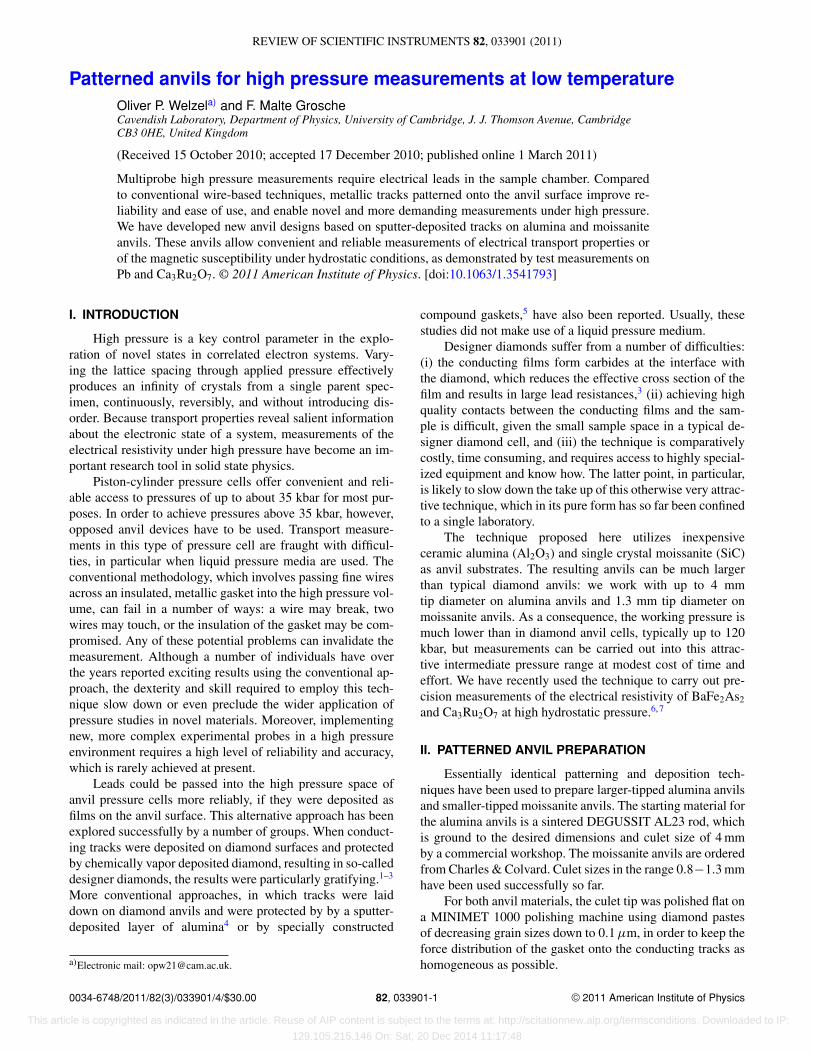
FIG. 1. (Color online) Patterned anvil designs. (a) Al2O3 anvil with eight-lead probe W pattern, (b) moissanite anvil with eight-lead probe NiCr pattern,and (c) Au on NiCr multilayered coil pattern on an Al2O3 anvil (bright areasrepresent metallic tracks in all three cases, see text for details).
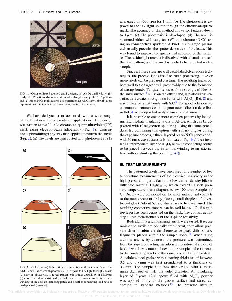
We have designed a master mask with a wide rangeof track patterns for a variety of applications. This designwas written onto a 3′′ × 3′′ chrome-on-quartz ultraviolet (UV)mask using electron-beam lithography (Fig. 1). Conven-tional photolithography was then applied to pattern the anvils(Fig. 2): (a) The anvils are spin coated with photoresist S1813
FIG. 2. (Color online) Fabricating a conducting coil on the surface of anAl2O3 anvil. (a) coat with photoresist, (b) expose to UV light through a mask,(c) develop photoresist to reveal pattern, (d) sputter deposit W or NiCr/Au,(e) remove residual resist, and (f) final pattern. To connect to the innermostwinding of the coil, an insulating patch and a further conducting lead have tobe deposited (see text).
at a speed of 4000 rpm for 1 min. (b) The photoresist is ex-posed to the UV light source through the chrome-on-quartzmask. The accuracy of this method allows for features downto 1 μm. (c) The photoresist is developed. (d) The anvil issputtered either with tungsten (W) or nichrome (NiCr) us-ing an rf-magnetron sputterer. A brief in situ argon plasmaetch usually precedes the sputter deposition of the leads. Thiswas found to improve the quality and adhesion of the tracks.(e) The residual photoresist is dissolved with ethanol to revealthe final pattern, and the anvil is ready to be mounted with asample.
Since all these steps are well established clean room tech-niques, the process lends itself to batch processing. Five ormore anvils can be prepared at a time. The resulting tracks ad-here well to the target anvil, presumably due to the formationof strong bonds. Tungsten tends to form strong carbides onthe anvil surface.3 NiCr, on the other hand, is particularly ver-satile, as it creates strong ionic bonds with Al2O3 (Ref. 8) andalso strong covalent bonds with SiC.9 The good adhesion weencountered contrasts with the poor track adhesion describedin Ref. 4, who deposited molybdenum onto diamond.
It is possible to create more complex patterns by includ-ing intermediate insulating layers of Al2O3, which can be de-posited with rf-magnetron sputtering, using the same proce-dure. By combining this option with a mask aligner duringthe exposure process, a three-layered Au on NiCr pancake coilwith 30 turns was successfully fabricated [Fig. 1(c)]. An insu-lating intermediate layer of Al2O3 allows a conducting bridgeto be placed between the innermost winding to an externallead without shorting the coil [Fig. 2(f)].
III. TEST MEASUREMENTS
The patterned anvils have been used for a number of lowtemperature measurements of the electrical resistivity underhigh pressure, in particular in the low carrier density bilayerruthenate material Ca3Ru2O7, which exhibits a rich pres-sure temperature phase diagram below 100 kbar. Samples ofCa3Ru2O7 were positioned on the anvil surface and contactsto the tracks were made by placing small droplets of silver-loaded glue (DuPont 6838), which have to be oven cured. Theresulting contact resistances can be well below 1 �, if a goldtop layer has been deposited on the track. The contact geom-etry allows measurements of the in-plane resistivity.
Both alumina and moissanite anvils were tested. Becausemoissanite anvils are optically transparent, they allow pres-sure determination via the fluorescence peak shift of rubyfragments placed within the sample space.10 When usingalumina anvils, by contrast, the pressure was determinedfrom the superconducting transition temperature of a piece oflead,11 which was mounted next to the sample and connectedto the conducting tracks in the same way as the sample itself.A stainless steel gasket with a starting thickness of between0.5 and 0.7 mm was first preindented to a thickness of0.2 mm. The sample hole was then drilled with a maxi-mum diameter of half the culet diameter. An insulatinglayer of Stycast 1266 epoxy filled with Al2O3 powderwas applied thinly to the gasket surface and cured ac-cording to standard methods.12 The pressure medium
This article is copyrighted as indicated in the article. Reuse of AIP content is subject to the terms at: http://scitationnew.aip.org/termsconditions. Downloaded to IP:
129.105.215.146 On: Sat, 20 Dec 2014 11:17:48
033901-3 O. P. Welzel and F. M. Grosche Rev. Sci. Instrum. 82, 033901 (2011)
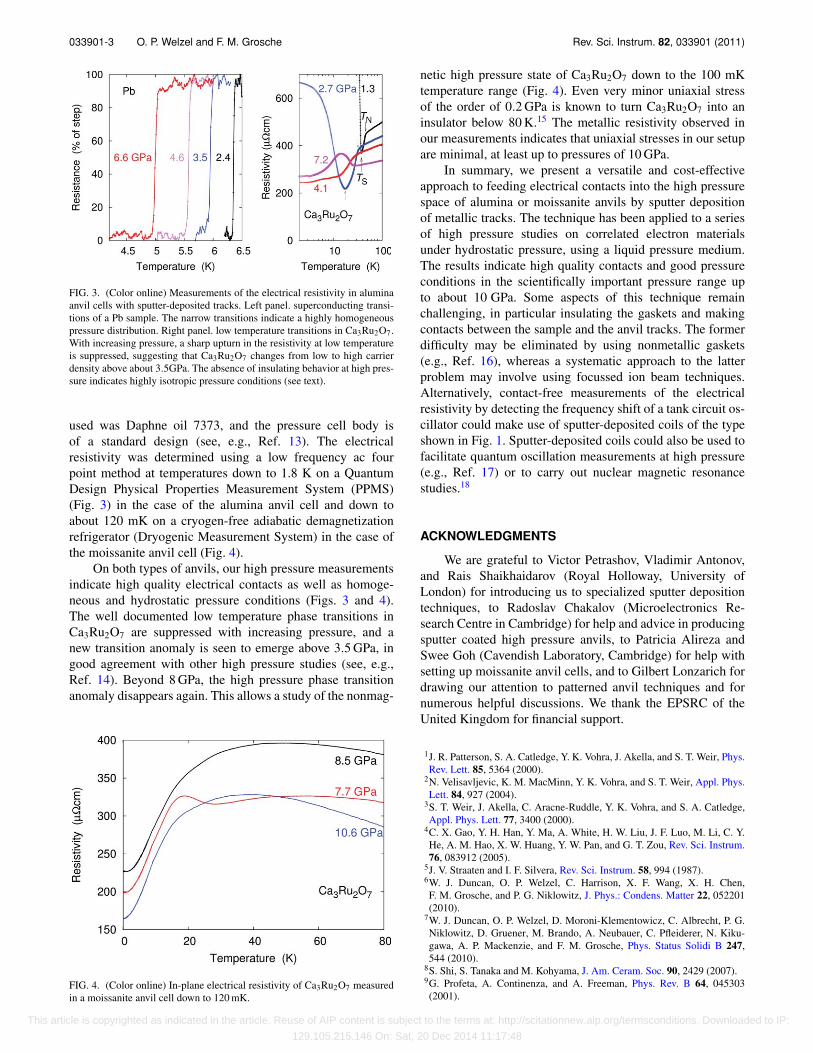
FIG. 3. (Color online) Measurements of the electrical resistivity in aluminaanvil cells with sputter-deposited tracks. Left panel. superconducting transi-tions of a Pb sample. The narrow transitions indicate a highly homogeneouspressure distribution. Right panel. low temperature transitions in Ca3Ru2O7.With increasing pressure, a sharp upturn in the resistivity at low temperatureis suppressed, suggesting that Ca3Ru2O7 changes from low to high carrierdensity above about 3.5GPa. The absence of insulating behavior at high pres-sure indicates highly isotropic pressure conditions (see text).
used was Daphne oil 7373, and the pressure cell body isof a standard design (see, e.g., Ref. 13). The electricalresistivity was determined using a low frequency ac fourpoint method at temperatures down to 1.8 K on a QuantumDesign Physical Properties Measurement System (PPMS)(Fig. 3) in the case of the alumina anvil cell and down toabout 120 mK on a cryogen-free adiabatic demagnetizationrefrigerator (Dryogenic Measurement System) in the case ofthe moissanite anvil cell (Fig. 4).
On both types of anvils, our high pressure measurementsindicate high quality electrical contacts as well as homoge-neous and hydrostatic pressure conditions (Figs. 3 and 4).The well documented low temperature phase transitions inCa3Ru2O7 are suppressed with increasing pressure, and anew transition anomaly is seen to emerge above 3.5 GPa, ingood agreement with other high pressure studies (see, e.g.,Ref. 14). Beyond 8 GPa, the high pressure phase transitionanomaly disappears again. This allows a study of the nonmag-
FIG. 4. (Color online) In-plane electrical resistivity of Ca3Ru2O7 measuredin a moissanite anvil cell down to 120 mK.
netic high pressure state of Ca3Ru2O7 down to the 100 mKtemperature range (Fig. 4). Even very minor uniaxial stressof the order of 0.2 GPa is known to turn Ca3Ru2O7 into aninsulator below 80 K.15 The metallic resistivity observed inour measurements indicates that uniaxial stresses in our setupare minimal, at least up to pressures of 10 GPa.
In summary, we present a versatile and cost-effectiveapproach to feeding electrical contacts into the high pressurespace of alumina or moissanite anvils by sputter depositionof metallic tracks. The technique has been applied to a seriesof high pressure studies on correlated electron materialsunder hydrostatic pressure, using a liquid pressure medium.The results indicate high quality contacts and good pressureconditions in the scientifically important pressure range upto about 10 GPa. Some aspects of this technique remainchallenging, in particular insulating the gaskets and makingcontacts between the sample and the anvil tracks. The formerdifficulty may be eliminated by using nonmetallic gaskets(e.g., Ref. 16), whereas a systematic approach to the latterproblem may involve using focussed ion beam techniques.Alternatively, contact-free measurements of the electricalresistivity by detecting the frequency shift of a tank circuit os-cillator could make use of sputter-deposited coils of the typeshown in Fig. 1. Sputter-deposited coils could also be used tofacilitate quantum oscillation measurements at high pressure(e.g., Ref. 17) or to carry out nuclear magnetic resonancestudies.18
ACKNOWLEDGMENTS
We are grateful to Victor Petrashov, Vladimir Antonov,and Rais Shaikhaidarov (Royal Holloway, University ofLondon) for introducing us to specialized sputter depositiontechniques, to Radoslav Chakalov (Microelectronics Re-search Centre in Cambridge) for help and advice in producingsputter coated high pressure anvils, to Patricia Alireza andSwee Goh (Cavendish Laboratory, Cambridge) for help withsetting up moissanite anvil cells, and to Gilbert Lonzarich fordrawing our attention to patterned anvil techniques and fornumerous helpful discussions. We thank the EPSRC of theUnited Kingdom for financial support.
1J. R. Patterson, S. A. Catledge, Y. K. Vohra, J. Akella, and S. T. Weir, Phys.Rev. Lett. 85, 5364 (2000).
2N. Velisavljevic, K. M. MacMinn, Y. K. Vohra, and S. T. Weir, Appl. Phys.Lett. 84, 927 (2004).
3S. T. Weir, J. Akella, C. Aracne-Ruddle, Y. K. Vohra, and S. A. Catledge,Appl. Phys. Lett. 77, 3400 (2000).
4C. X. Gao, Y. H. Han, Y. Ma, A. White, H. W. Liu, J. F. Luo, M. Li, C. Y.He, A. M. Hao, X. W. Huang, Y. W. Pan, and G. T. Zou, Rev. Sci. Instrum.76, 083912 (2005).
5J. V. Straaten and I. F. Silvera, Rev. Sci. Instrum. 58, 994 (1987).6W. J. Duncan, O. P. Welzel, C. Harrison, X. F. Wang, X. H. Chen,F. M. Grosche, and P. G. Niklowitz, J. Phys.: Condens. Matter 22, 052201(2010).
7W. J. Duncan, O. P. Welzel, D. Moroni-Klementowicz, C. Albrecht, P. G.Niklowitz, D. Gruener, M. Brando, A. Neubauer, C. Pfleiderer, N. Kiku-gawa, A. P. Mackenzie, and F. M. Grosche, Phys. Status Solidi B 247,544 (2010).
8S. Shi, S. Tanaka and M. Kohyama, J. Am. Ceram. Soc. 90, 2429 (2007).9G. Profeta, A. Continenza, and A. Freeman, Phys. Rev. B 64, 045303(2001).
This article is copyrighted as indicated in the article. Reuse of AIP content is subject to the terms at: http://scitationnew.aip.org/termsconditions. Downloaded to IP:
129.105.215.146 On: Sat, 20 Dec 2014 11:17:48

033901-4 O. P. Welzel and F. M. Grosche Rev. Sci. Instrum. 82, 033901 (2011)
10H. Mao, J. Xu, and P. M. Bell, J. Geophys. Research-Solid Earth 91, 4673(1986).
11T. F. Smith, C. W. Chu, and M. B. Maple, Cryogenics 9, 53 (1969).12J. Thomasson, Y. Dumont, J. Griveau, and C. Ayache, Rev. Sci. Instrum.
68, 1514 (1997).13D. Dunstan and I. Spain, J. Phys. E 22, 913 (1989).14Y. Yoshida, M. Hedo, S. I. Ikeda, N. Shirakawa, and Y. Uwatoko, Physica B
403, 1213 (2008).
15G. Cao, L. Balicas, Y. Xin, J. Crow, and C. Nelson, Phys. Rev. B 67, 184405(2003).
16D. Jaccard and K. Sengupta, Rev. Sci. Instrum. 81, 043908 (2010).17S. K. Goh, P. L. Alireza, P. D.A. Mann, A. M. Curnberlidge, C.
Bergernann, M. Sutherland, and Y. Maeno, Curr. Appl. Phys. 8, 304(2008).
18J. Haase, S. K. Goh, T. Meissner, P. L. Alireza, and D. Rybicki, Rev. Sci.Instrum. 80, 073905 (2009).
This article is copyrighted as indicated in the article. Reuse of AIP content is subject to the terms at: http://scitationnew.aip.org/termsconditions. Downloaded to IP:
129.105.215.146 On: Sat, 20 Dec 2014 11:17:48