Embed Size (px)
DESCRIPTION
Pathways to new magnetic semiconductors and half metals. G.A.Sawatzky. Department of Physics and Astronomy, University of British Columbia, Canada. I.Elfimov UBC S.Yunoki Trieste P.Steeneken Philips H. Tjeng Cologne A.Damascelli UBC K.Shen UBC D.Hawthorn UBC N.Ingle UBCb. - PowerPoint PPT Presentation
Citation preview
G.A.Sawatzky
Pathways to new magnetic semiconductors and half metals
Department of Physics and Astronomy, University of British Columbia, Canada

collaborators
• I.Elfimov UBC• S.Yunoki Trieste• P.Steeneken Philips• H. Tjeng Cologne• A.Damascelli UBC• K.Shen UBC• D.Hawthorn UBC• N.Ingle UBCb
• T.Hibma Groningen• P.Abbamonte Illinois• A.Rushdy Hamburg
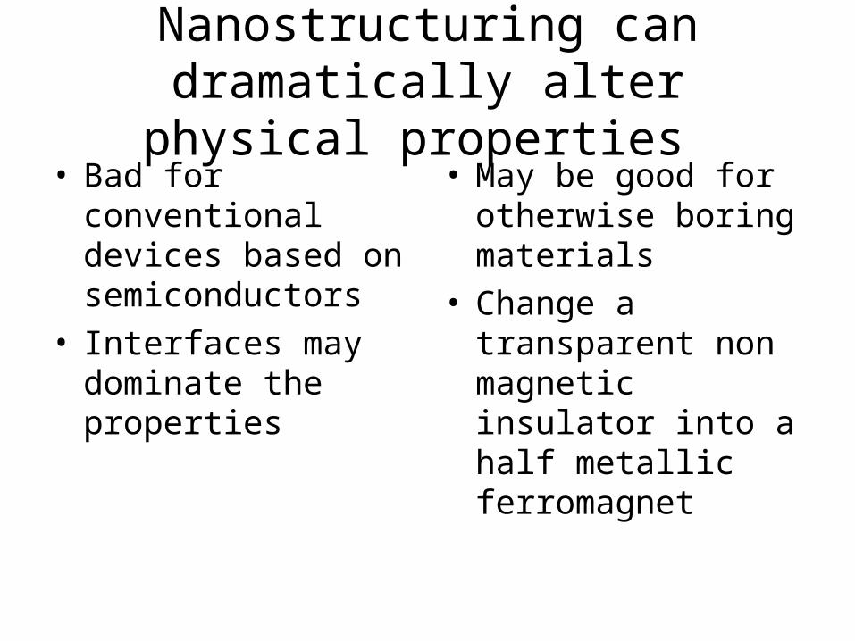
Nanostructuring can dramatically alter physical properties
• Bad for conventional devices based on semiconductors
• Interfaces may dominate the properties
• May be good for otherwise boring materials
• Change a transparent non magnetic insulator into a half metallic ferromagnet
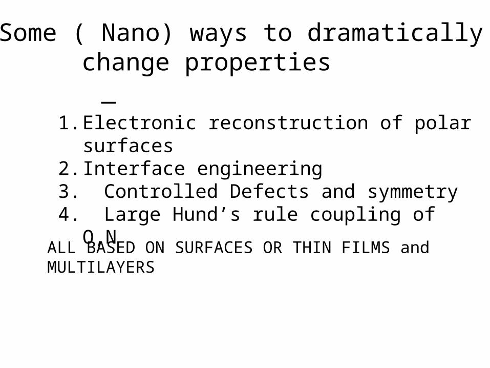
Some ( Nano) ways to dramatically change properties
1. Electronic reconstruction of polar surfaces2. Interface engineering 3. Controlled Defects and symmetry4. Large Hund’s rule coupling of O,N
ALL BASED ON SURFACES OR THIN FILMS and MULTILAYERS
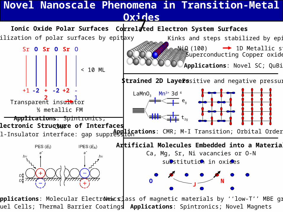
Novel Nanoscale Phenomena in Transition-Metal Oxides
Ionic Oxide Polar Surfaces
Stabilization of polar surfaces by epitaxy
Transparent insulator ½ metallic FM
Applications: Spintronics; CMR
SrO O
-1+2-2
Sr SrO
+1 +2-2
< 10 ML
Artificial Molecules Embedded into a MaterialCa, Mg, Sr, Ni vacancies or O-N substitution in oxides
New class of magnetic materials by ‘‘low-T’’ MBE growthApplications: Spintronics; Novel Magnets
JO N
LaMnO3
eg
t2g
Mn3+ 3d 4
Strained 2D Layers Positive and negative pressure
Applications: CMR; M-I Transition; Orbital Ordering
Correlated Electron System Surfaces
Kinks and steps stabilized by epitaxy
NiO (100) 1D Metallic stepsSuperconducting Copper oxides
Applications: Novel SC; QuBits
Electronic Structure of InterfacesMetal-Insulator interface: gap suppression
Applications: Molecular Electronics;Fuel Cells; Thermal Barrier Coatings
7
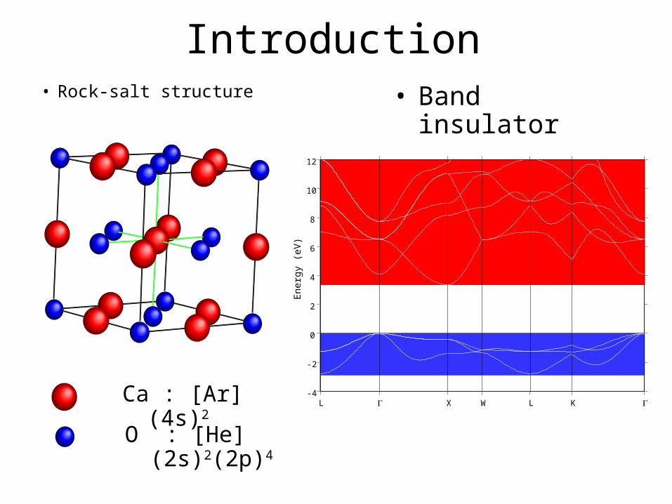
Introduction• Rock-salt structure • Band insulator
Ca : [Ar](4s)2
O : [He](2s)2(2p)4
-4
-2
0
2
4
6
8
10
12
L X W L K
Ene
rgy
(eV
)
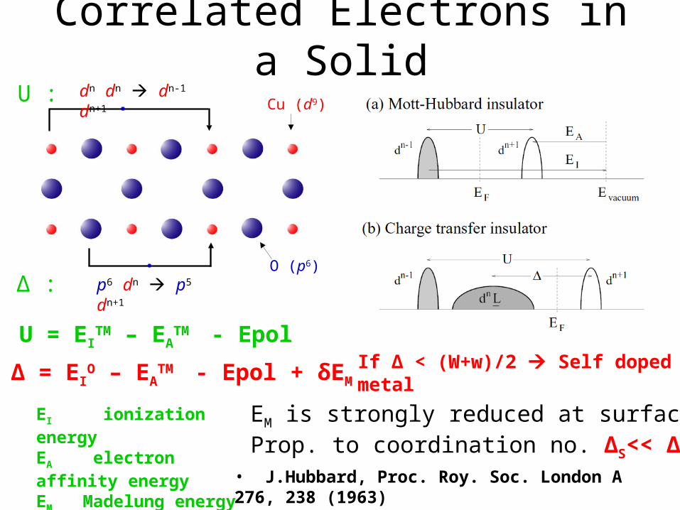
Correlated Electrons in a Solid
• J.Hubbard, Proc. Roy. Soc. London A 276, 238 (1963)• ZSA, PRL 55, 418 (1985)
If Δ < (W+w)/2 Self doped metal
dn dn dn-1 dn+1U :
p6 dn p5 dn+1Δ :
U = EITM – EA
TM - Epol
Δ = EIO – EA
TM - Epol + δEM
EI ionization energyEA electron affinity energyEM Madelung energy
Cu (d9)
O (p6)
EM is strongly reduced at surfacesProp. to coordination no. ΔS<< ΔB
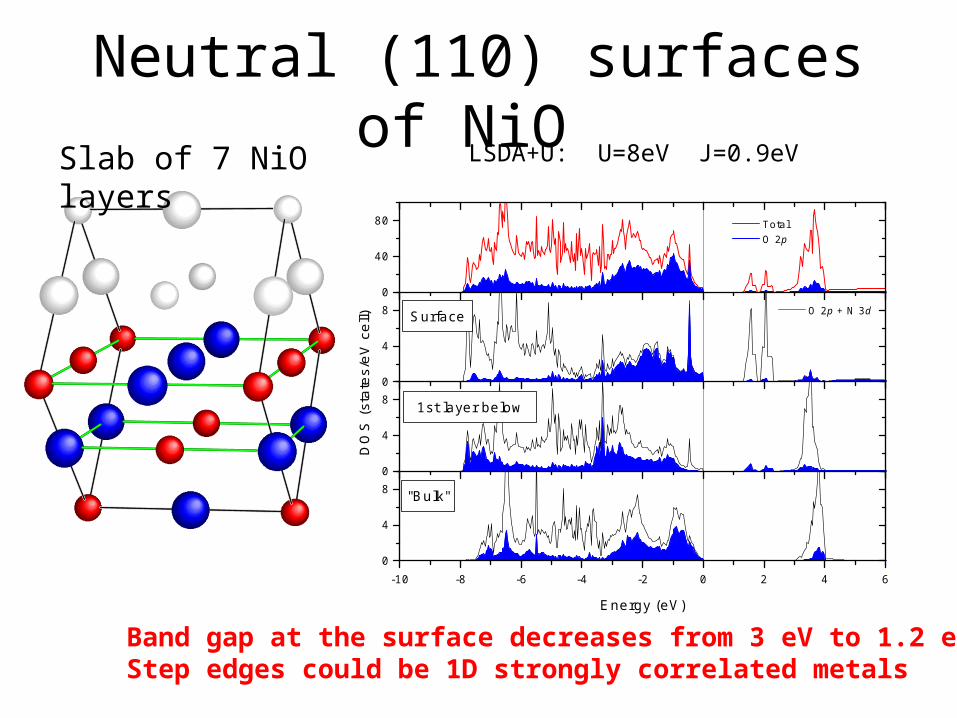
Neutral (110) surfaces of NiO
-10 -8 -6 -4 -2 0 2 4 60
4
8 "Bulk"
Energy (eV)
0
4
8 1st layer below
0
4
8 Surface O 2p + N 3d
DO
S (
stat
es/e
V c
ell)
0
40
80
Total O 2p
LSDA+U: U=8eV J=0.9eVSlab of 7 NiO layers
Band gap at the surface decreases from 3 eV to 1.2 eVStep edges could be 1D strongly correlated metals
POLAR SURFACES
For review see Noguera J.Phys. Condens Matter 12 (2000) R367)
ELECTRONIC RECONSTRUCTION
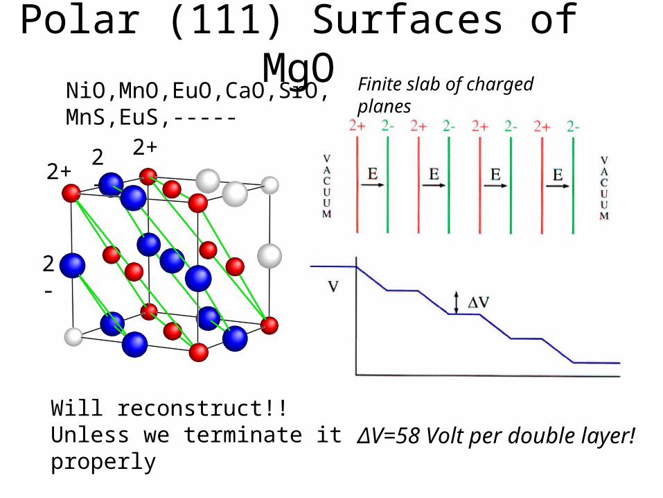
Polar (111) Surfaces of MgO
2-
2+
Finite slab of charged planes
ΔV=58 Volt per double layer!
2- 2+
NiO,MnO,EuO,CaO,SrO,MnS,EuS,-----
Will reconstruct!!Unless we terminate itproperly
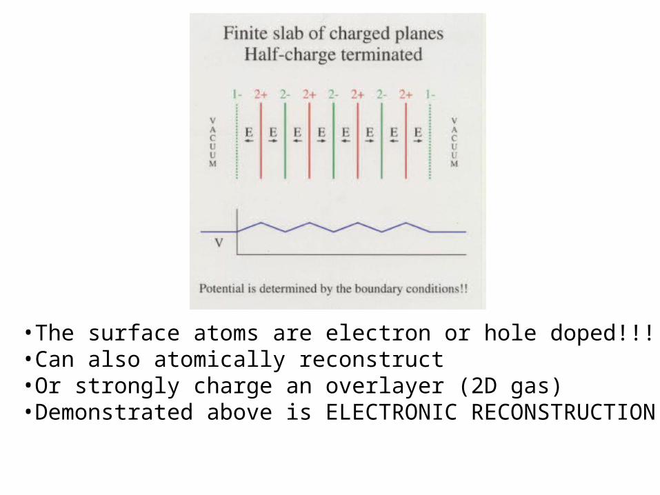
•The surface atoms are electron or hole doped!!!•Can also atomically reconstruct•Or strongly charge an overlayer (2D gas)•Demonstrated above is ELECTRONIC RECONSTRUCTION
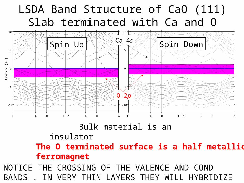
LSDA Band Structure of CaO (111) Slab terminated with Ca and O
-10
-5
0
5
10
Γ K M Γ A L H A
Ene
rgy
(eV
)
-10
-5
0
5
10
Γ K M Γ A L H A
Spin Up Spin Down
Bulk material is an insulator
Ca 4s
O 2p
The O terminated surface is a half metallic ferromagnet
NOTICE THE CROSSING OF THE VALENCE AND CONDBANDS . IN VERY THIN LAYERS THEY WILL HYBRIDIZE
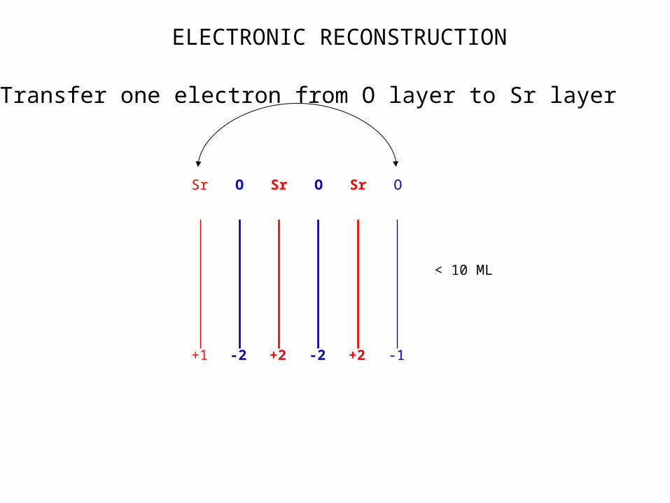
SrO O
-1+2-2
Sr SrO
+1 +2-2
< 10 ML
Transfer one electron from O layer to Sr layer
ELECTRONIC RECONSTRUCTION
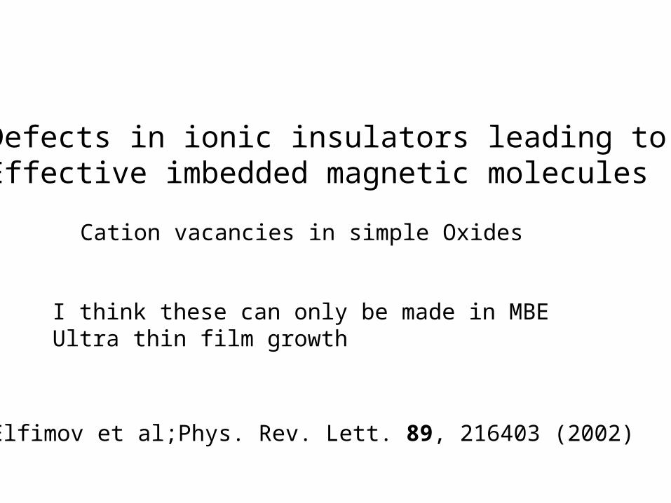
Defects in ionic insulators leading to Effective imbedded magnetic molecules
Cation vacancies in simple Oxides
Elfimov et al;Phys. Rev. Lett. 89, 216403 (2002)
I think these can only be made in MBEUltra thin film growth
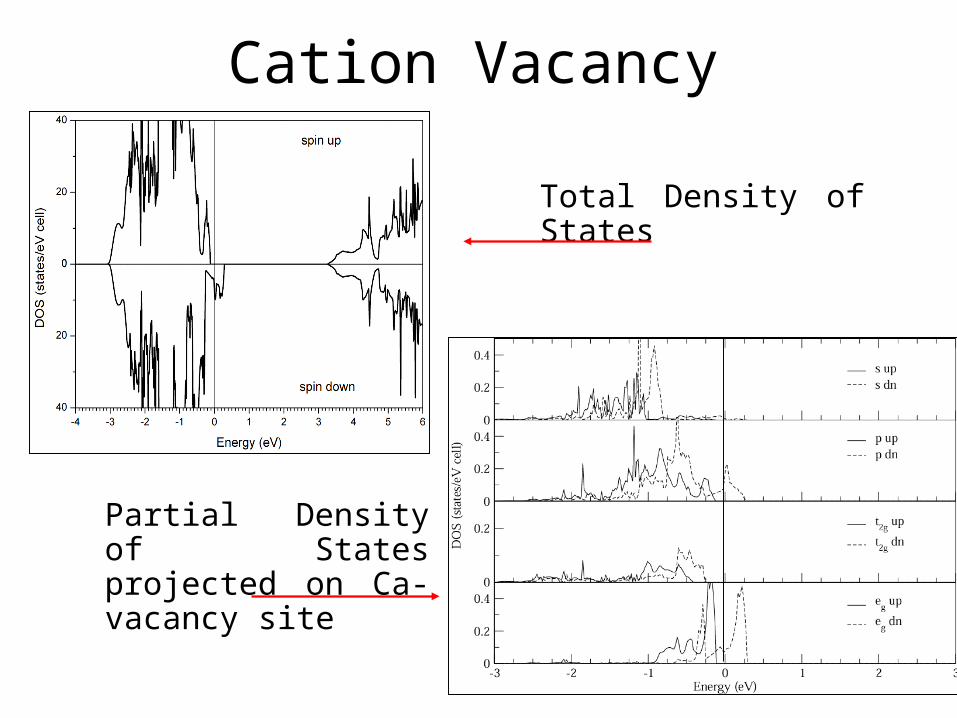
Cation Vacancy
Partial Density of States projected on Ca-vacancy site
Total Density of States
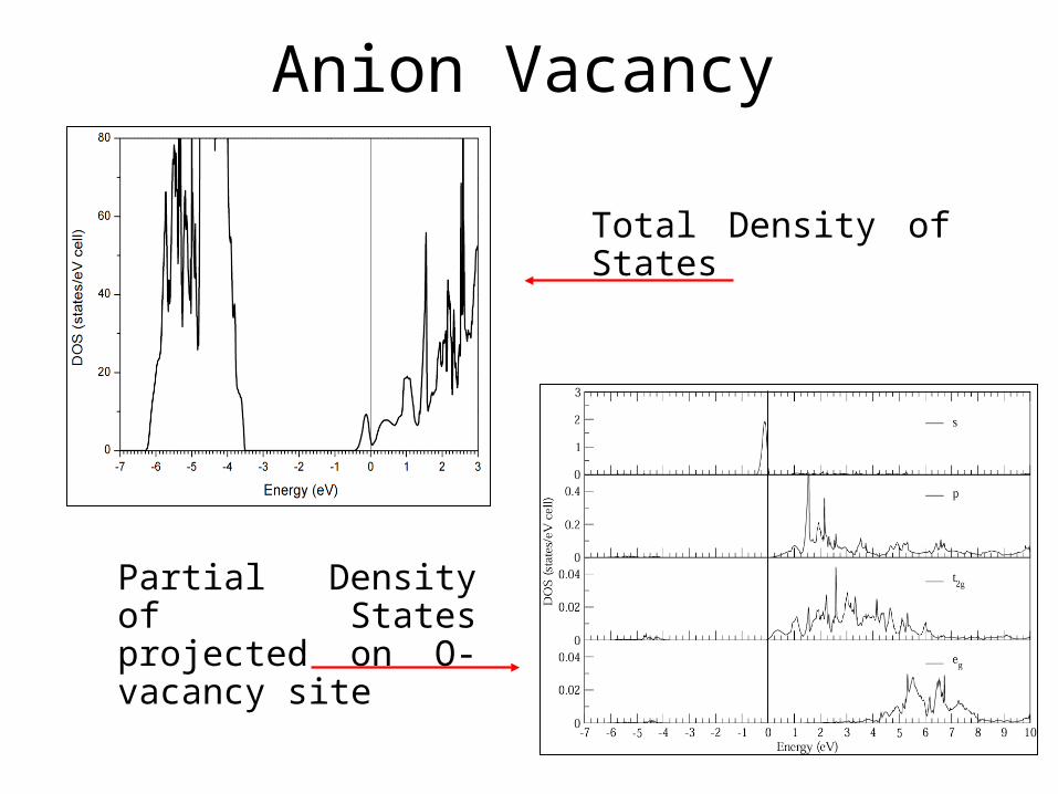
Anion Vacancy
Partial Density of States projected on O-vacancy site
Total Density of States
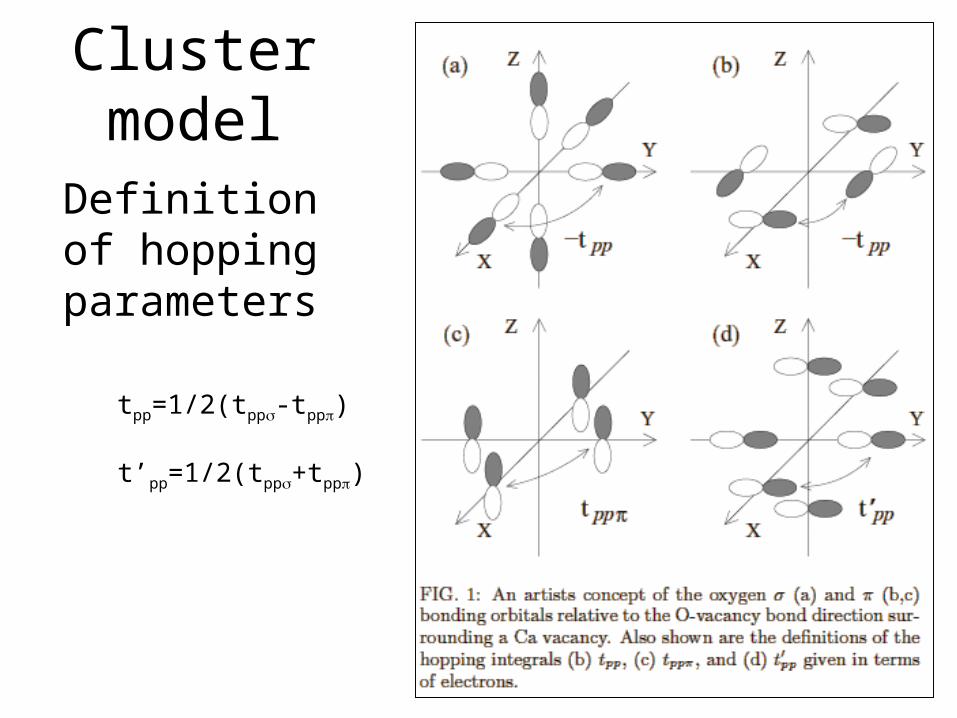
Definition of hopping
parameters
tpp=1/2(tpp-tpp)
t’pp=1/2(tpp+tpp)
Cluster model
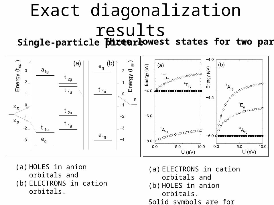
Exact diagonalization results Single-particle picture Three lowest states for two particles
(a) HOLES in anion orbitals and (b) ELECTRONS in cation
orbitals.
(a) ELECTRONS in cation orbitals and
(b) HOLES in anion orbitals.Solid symbols are for triplet state
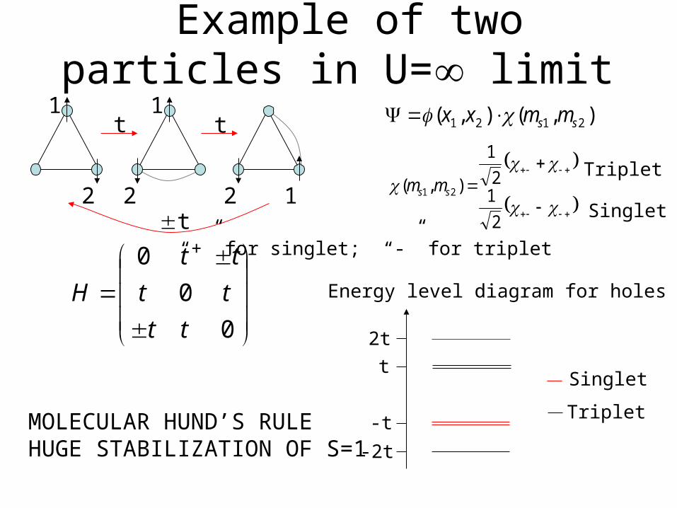
Example of two particles in U= limit
t t
t
1 1
2 2 2 1
0
0
0
tt
tt
tt
H
),(),( 2121 ss mmxx
2
12
1
),( 21 ss mmTriplet
Singlet
“+” for singlet; “-” for triplet
Energy level diagram for holes (t>0)
-2t
-t
t
2t
Triplet
Singlet
MOLECULAR HUND’S RULE HUGE STABILIZATION OF S=1
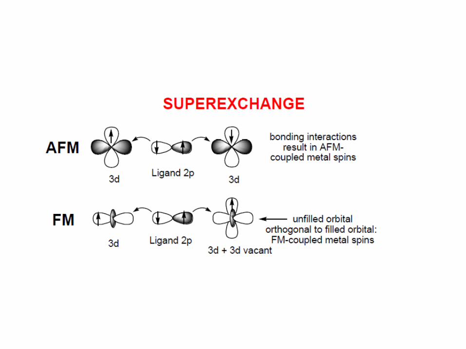
• Point structural defects in crystals such as vacancies can indeed confine the compensating charges in molecular orbitals formed by atomic orbitals on the nearest neighbours.
• Under certain conditions “local” magnetic moments will be formed due to a kind of molecular Hund’s rule coupling with energetic determined by kinetic energy and symmetry considerations rather than exchange interactions.
Strange magnetic materials
• This could be the origin of the high Tc materials such as Co in TiO2, or ZnO, or in oxides of non magnetic materials like HfO2
• Prelier et al Phys Cond. Matter 15,R1583 (2003)
• Venkatesan et al Nature 430, 630 ( 2004)
Anion substitution Replace O with N
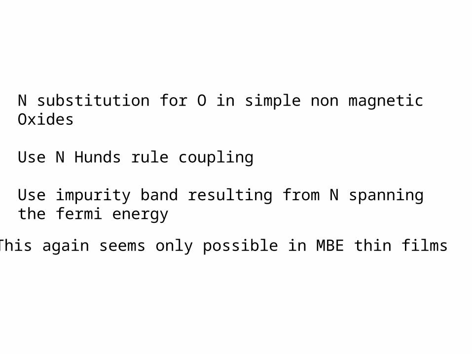
N substitution for O in simple non magnetic Oxides
Use N Hunds rule coupling
Use impurity band resulting from N spanning the fermi energy
This again seems only possible in MBE thin films
3
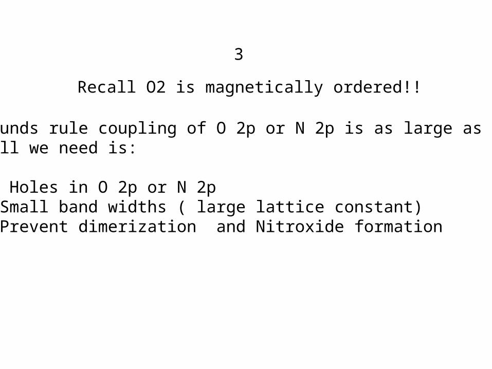
Hunds rule coupling of O 2p or N 2p is as large as Mn!!!All we need is:
• Holes in O 2p or N 2p•Small band widths ( large lattice constant) •Prevent dimerization and Nitroxide formation
Recall O2 is magnetically ordered!!
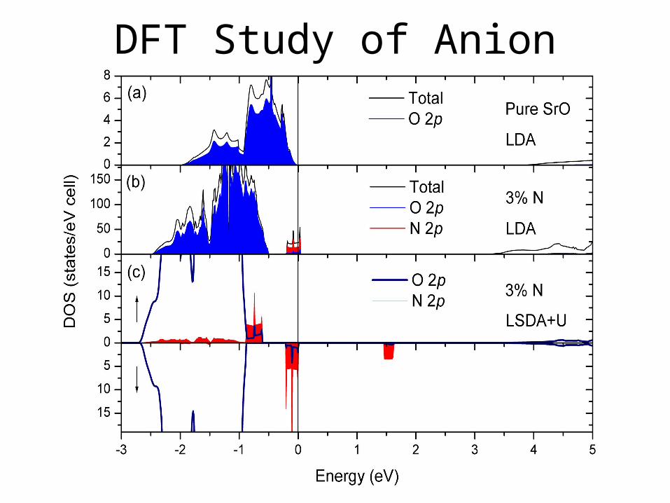
DFT Study of Anion Substitution in SrO
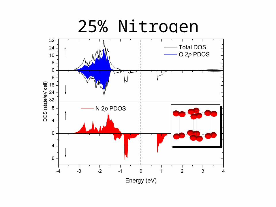
25% Nitrogen
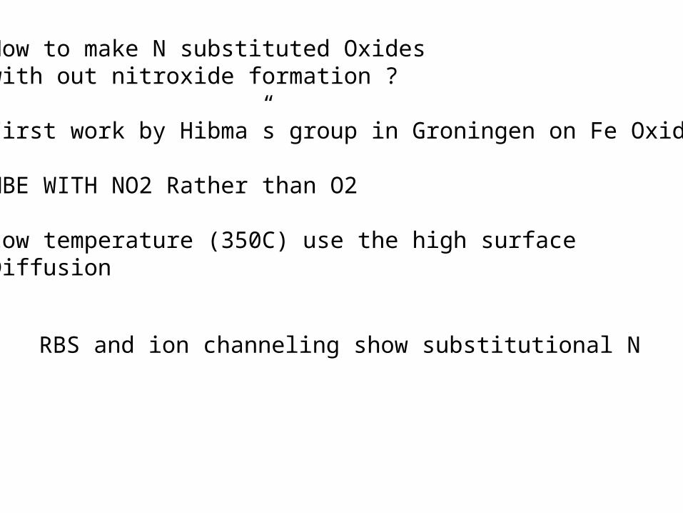
How to make N substituted Oxides with out nitroxide formation ?
First work by Hibma”s group in Groningen on Fe Oxides
MBE WITH NO2 Rather than O2
Low temperature (350C) use the high surface Diffusion
RBS and ion channeling show substitutional N
9 8 7 6 5 4 3 2 1 Ef = 0 -1 -23000
3500
4000
4500
5000
5500
6000
6500
7000
7500
O2p
N2p
Co
un
t Ra
te
Binding Energy (eV)
XPS with MgK-sourceT=293 K
SrO SrO
0.82N
0.18
SrO0.75
N0.25
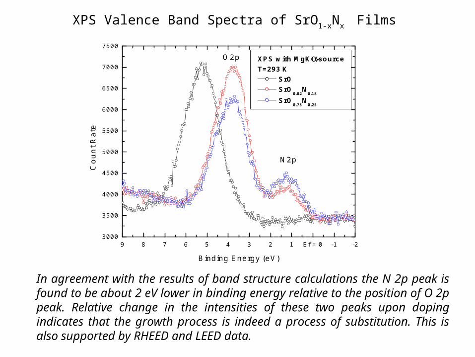
XPS Valence Band Spectra of SrO1-xNx Films
In agreement with the results of band structure calculations the N 2p peak is found to be about 2 eV lower in binding energy relative to the position of O 2p peak. Relative change in the intensities of these two peaks upon doping indicates that the growth process is indeed a process of substitution. This is also supported by RHEED and LEED data.
385 390 395 400 405 410 415 420 425 430 435 440 445
1.00
1.02
1.04
1.06
1.08
1.10
1.12
1.14 A
To
tal Y
ield
(n
orm
aliz
ed
)
Photon Energy (eV)
E||ab; T = 293 K SrO
0.80N
0.20
SrO0.70
N0.30
Ta3N
5
525 530 535 540 545 550 555 560 565 570 575
1.0
1.1
1.2
1.3
1.4
1.5
1.6
1.7
1.8
1.9
B
528 530 532 534 536
1.0
1.1
1.2
1.3
1.4
1.5
1.6
1.7
1.8
1.9
Total Yield (nor
malized)
Photon Energy (eV)
To
tal Y
ield
(n
orm
aliz
ed
)Photon Energy (eV)
E||ab; T = 293 K SrO SrO
0.80N
0.20
SrO0.70
N0.30
Nitrogen K-edge Oxygen K-edge
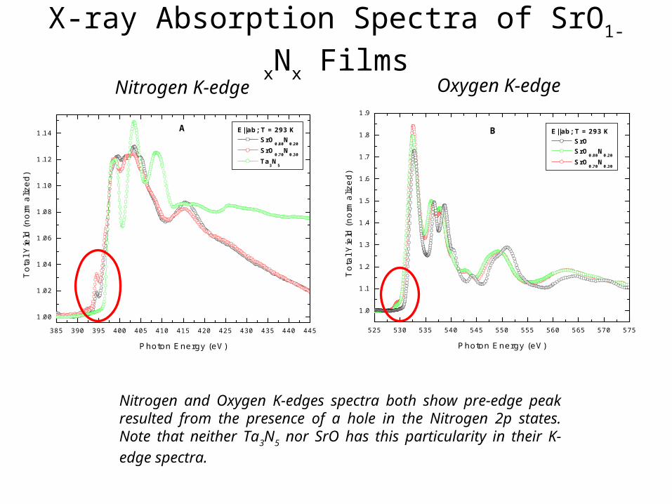
X-ray Absorption Spectra of SrO1-xNx Films
Nitrogen and Oxygen K-edges spectra both show pre-edge peak resulted from the presence of a hole in the Nitrogen 2p states. Note that neither Ta3N5 nor SrO has this particularity in their K-edge spectra.
402 401 400 399 398 397 396 395 394 393 392
36000
38000
40000
42000
44000
46000
2.91 eV1.63 eV
Peak 3
Peak 2
Peak 1
Peak1:Peak2:Peak3 = 3.95:1:0.14
Co
un
t Ra
te
Binding Energy (eV)
XPS with MgK-sourceT=293 K
SrO0.75
N0.25
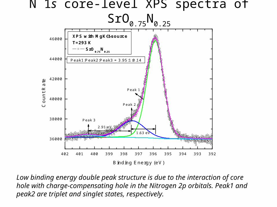
N 1s core-level XPS spectra of SrO0.75N0.25
Low binding energy double peak structure is due to the interaction of core hole with charge-compensating hole in the Nitrogen 2p orbitals. Peak1 and peak2 are triplet and singlet states, respectively.
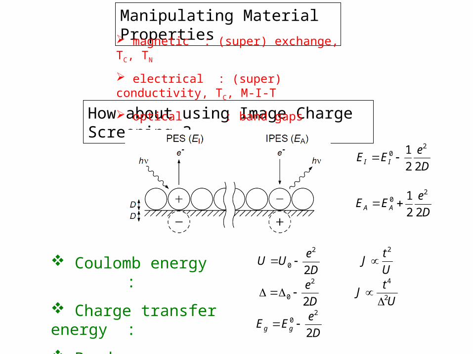
Manipulating Material Properties
How about using Image Charge Screening ?
magnetic : (super) exchange, TC, TN
electrical : (super) conductivity, TC, M-I-T
optical : band gaps
D
eEE II 22
1 20
D
eEE AA 22
1 20
Coulomb energy :
Charge transfer energy :
Band gap :
D
eUU
2
2
0
D
e
2
2
0
D
eEE gg 2
20
U
tJ
2
U
tJ
2
4
q ’ q
2 1R 1
R 2n
a
0
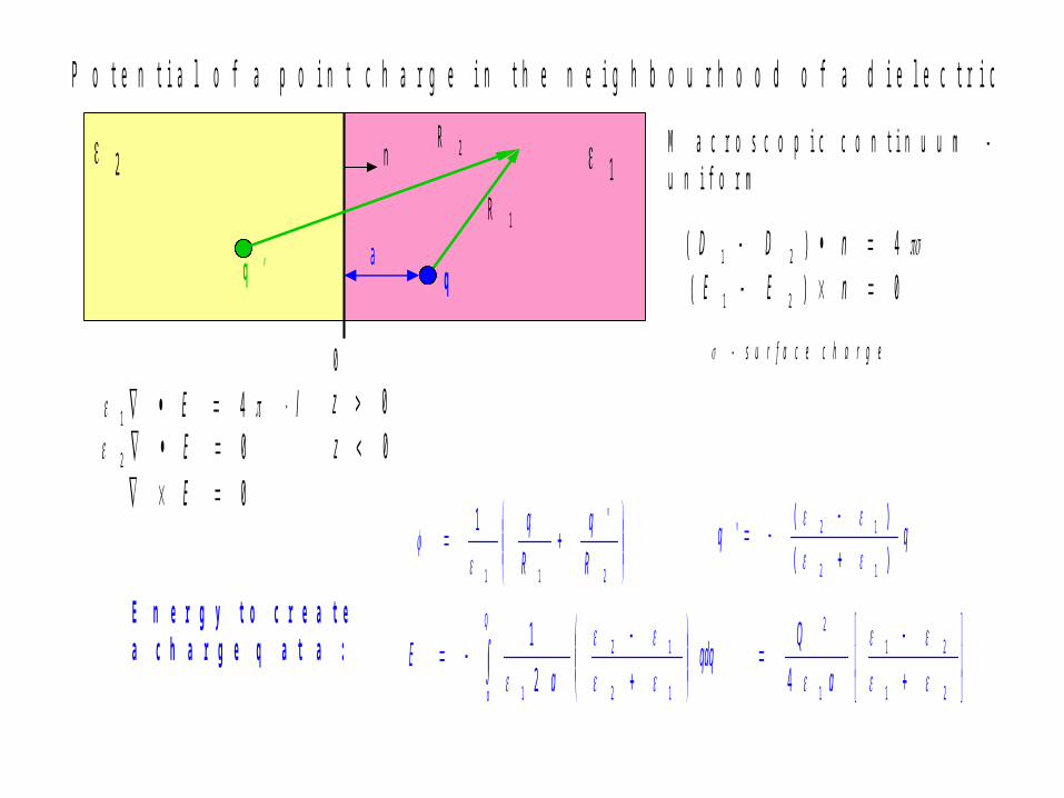
P o t e n t i a l o f a p o i n t c h a r g e i n t h e n e i g h b o u r h o o d o f a d i e l e c t r i c
M a c r o s c o p i c c o n t i n u u m -u n i f o r m
4)( 21 nDD
- s u r f a c e c h a r g e
0)( 21 nEE
lE 41
02 E0 E
0z0z
211
'1
R
q
R
q
)(
)('
12
12
E n e r g y t o c r e a t e a c h a r g e q a t a :
Q
o a
Qqdq
aE
21
21
1
2
12
12
1 42
1
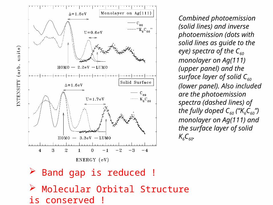
Combined photoemission (solid lines) and inverse photoemission (dots with solid lines as guide to the eye) spectra of the C60 monolayer on Ag(111) (upper panel) and the surface layer of solid C60 (lower panel). Also included are the photoemission spectra (dashed lines) of the fully doped C60 (“K6C60”) monolayer on Ag(111) and the surface layer of solid K6C60.
Band gap is reduced !
Molecular Orbital Structure is conserved !
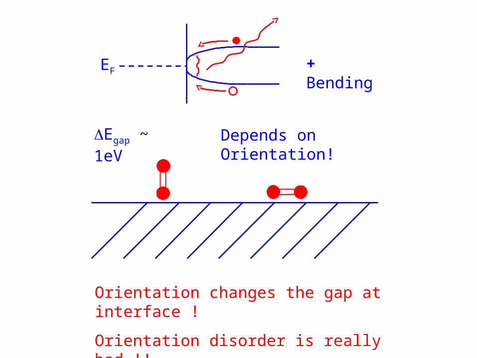
EF + Bending
Egap ~ 1eV Depends on Orientation!
Orientation changes the gap at interface !
Orientation disorder is really bad !!
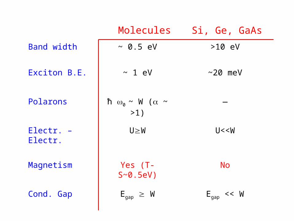
Band width ~ 0.5 eV >10 eV
Exciton B.E. ~ 1 eV ~20 meV
Polarons ћ 0 ~ W ( ~ >1) —
Electr. – Electr. UW U<<W
Magnetism Yes (T-S~0.5eV) No
Cond. Gap Egap W Egap << W
Si, Ge, GaAsMolecules
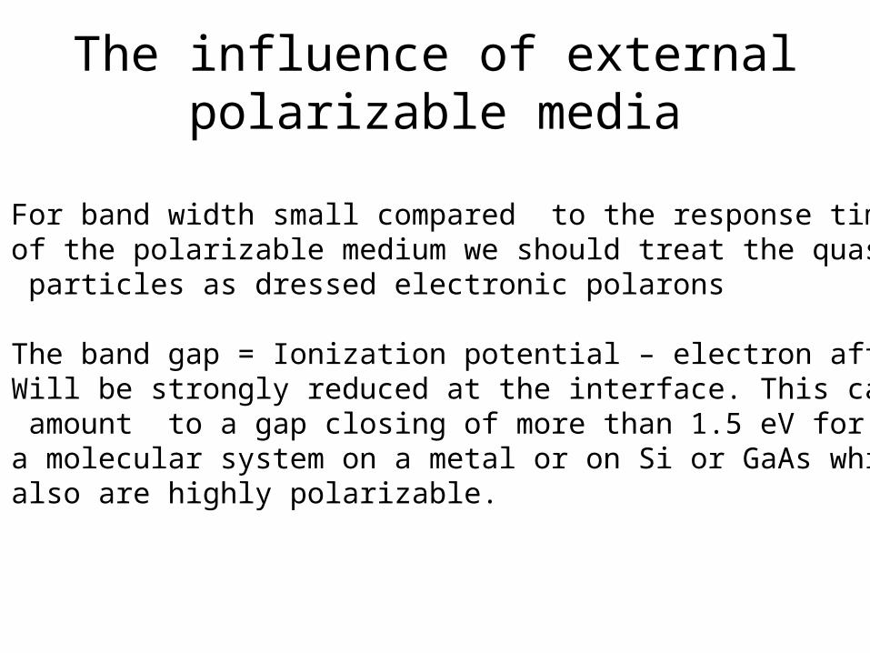
The influence of external polarizable media
For band width small compared to the response time of the polarizable medium we should treat the quasi particles as dressed electronic polarons
The band gap = Ionization potential – electron affinityWill be strongly reduced at the interface. This can amount to a gap closing of more than 1.5 eV for a molecular system on a metal or on Si or GaAs whichalso are highly polarizable.
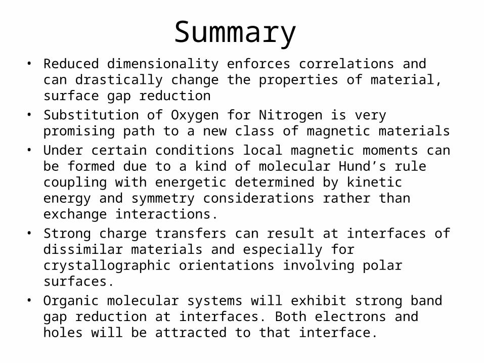
Summary• Reduced dimensionality enforces correlations and can drastically
change the properties of material, surface gap reduction• Substitution of Oxygen for Nitrogen is very promising path to a new
class of magnetic materials• Under certain conditions local magnetic moments can be formed
due to a kind of molecular Hund’s rule coupling with energetic determined by kinetic energy and symmetry considerations rather than exchange interactions.
• Strong charge transfers can result at interfaces of dissimilar materials and especially for crystallographic orientations involving polar surfaces.
• Organic molecular systems will exhibit strong band gap reduction at interfaces. Both electrons and holes will be attracted to that interface.