Embed Size (px)
Citation preview
1
1 Marco SAMPIETRO Organic transistors (I)
Advanced Course on
ORGANIC ELECTRONICS
Principles, devices and applications
ORGANIC THIN-FILM TRANSISTORS
Marco Sampietro
2 Marco SAMPIETRO Organic transistors (I)
Why being interested in OFET ?
NOT as a substitute of crystal Si !
TECNOLOGY COMPATIBILE with organic screen pixels
all plastic screen
DISPENSED at LOW TEMPERATURE and on flexible
substrates RFID
Hopefully, low cost and big dimensions
e-paper, active message board
2
3 Marco SAMPIETRO Organic transistors (I)
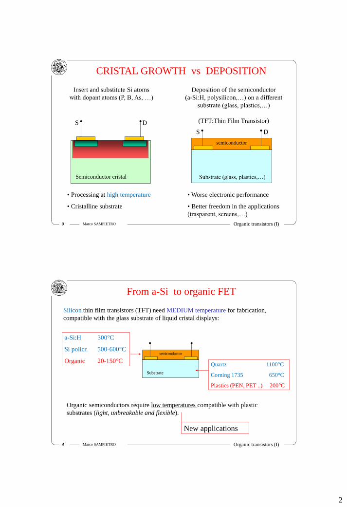
CRISTAL GROWTH vs DEPOSITION
• Processing at high temperature
• Cristalline substrate
• Worse electronic performance
• Better freedom in the applications
(trasparent, screens,…)
S D
Insert and substitute Si atoms
with dopant atoms (P, B, As, …)
Semiconductor cristal
S D
semiconductor
Deposition of the semiconductor
(a-Si:H, polysilicon,…) on a different
substrate (glass, plastics,…)
(TFT:Thin Film Transistor)
Substrate (glass, plastics,…)
4 Marco SAMPIETRO Organic transistors (I)
From a-Si to organic FET
Silicon thin film transistors (TFT) need MEDIUM temperature for fabrication,
compatible with the glass substrate of liquid cristal displays:
a-Si:H 300°C
Si policr. 500-600°C
Organic 20-150°C
semiconductor
Substrate
Quartz 1100°C
Corning 1735 650°C
Plastics (PEN, PET ..) 200°C
Organic semiconductors require low temperatures compatible with plastic
substrates (light, unbreakable and flexible).
New applications
3
5 Marco SAMPIETRO Organic transistors (I)
Mobility
Current modulation
Voltage of operation
Ambient stability Very good
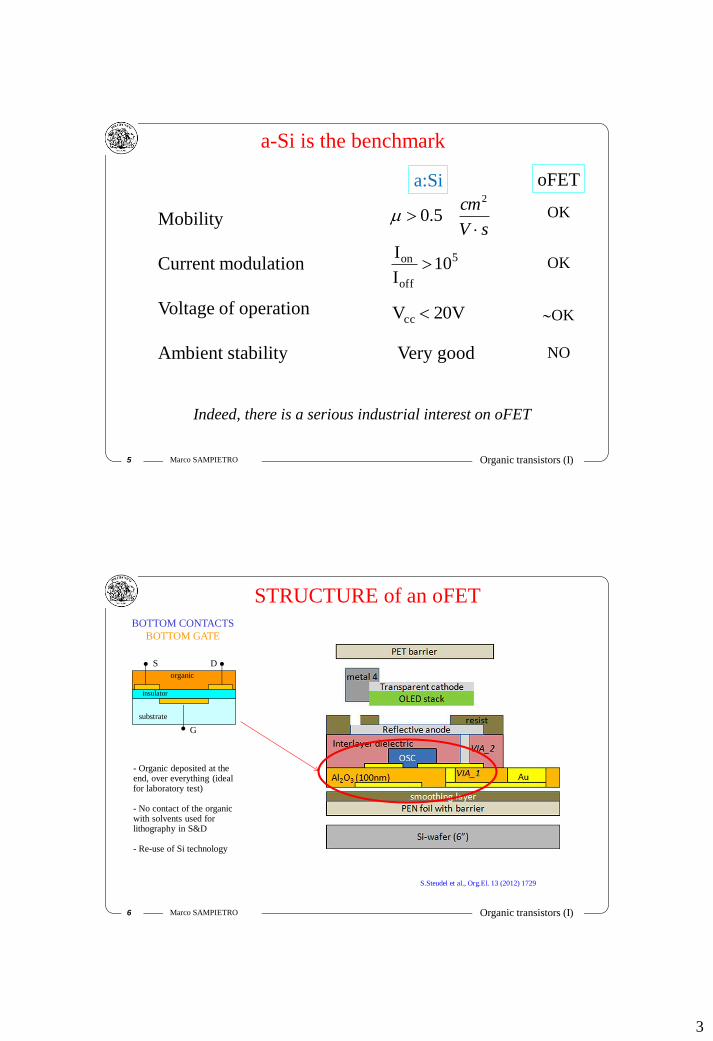
a-Si is the benchmark
sV
cm
2
5.0
5
off
on 10I
I
V20Vcc
oFET a:Si
OK
OK
OK
NO
Indeed, there is a serious industrial interest on oFET
6 Marco SAMPIETRO Organic transistors (I)
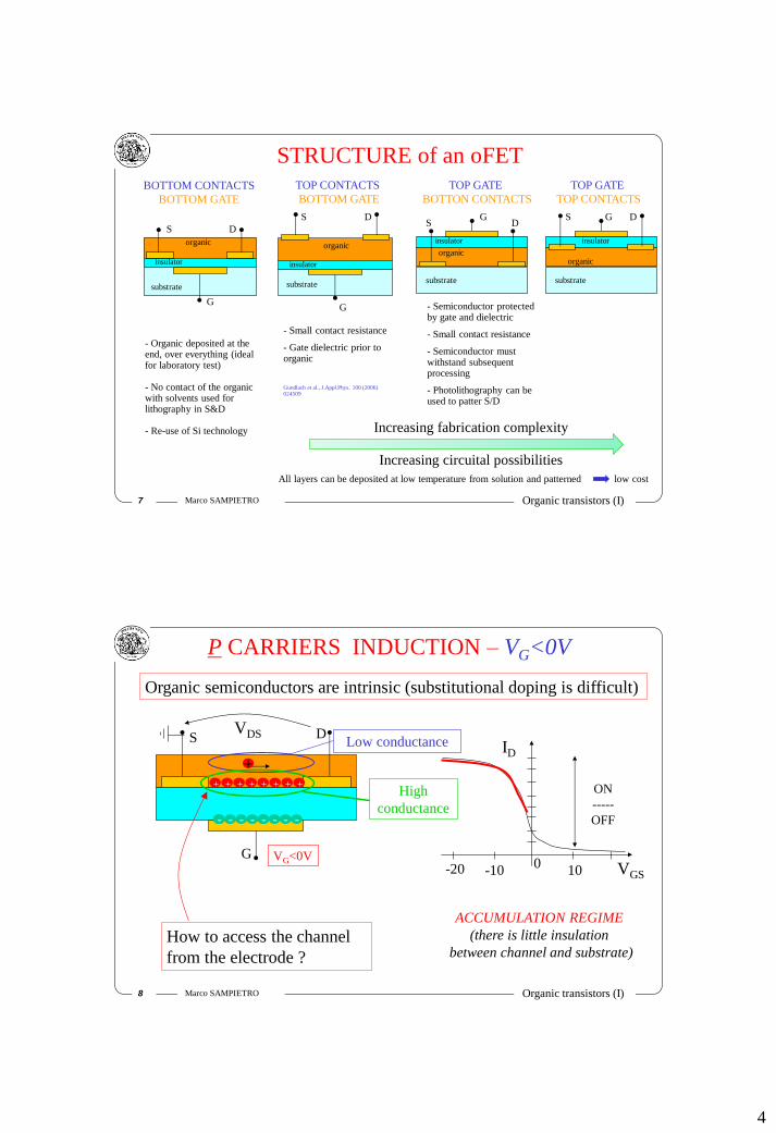
STRUCTURE of an oFET
BOTTOM CONTACTS
BOTTOM GATE
- Organic deposited at the end, over everything (ideal for laboratory test) - No contact of the organic with solvents used for lithography in S&D - Re-use of Si technology
insulator
substrate
G
S D
organic
S.Steudel et al., Org.El. 13 (2012) 1729
4
7 Marco SAMPIETRO Organic transistors (I)
STRUCTURE of an oFET
BOTTOM CONTACTS
BOTTOM GATE
- Organic deposited at the end, over everything (ideal for laboratory test) - No contact of the organic with solvents used for lithography in S&D - Re-use of Si technology
insulator
substrate
G
S D
organic
Increasing fabrication complexity
Increasing circuital possibilities
All layers can be deposited at low temperature from solution and patterned low cost
TOP CONTACTS
BOTTOM GATE
insulator
substrate
D S
G
organic insulator
substrate
organic
G S D
insulator
substrate
organic
G S D
TOP GATE
TOP CONTACTS
TOP GATE
BOTTON CONTACTS
- Small contact resistance
- Gate dielectric prior to organic
Gundlach et al., J.Appl.Phys. 100 (2006) 024509
- Semiconductor protected by gate and dielectric
- Small contact resistance
- Semiconductor must withstand subsequent processing
- Photolithography can be used to patter S/D
8 Marco SAMPIETRO Organic transistors (I)
ACCUMULATION REGIME
(there is little insulation
between channel and substrate)
VGS
ID
0 -20 -10 10
S D
G VG<0V
+ + + + + + + +
- - - - - - - - - -
P CARRIERS INDUCTION – VG<0V
VDS
+
Low conductance
High
conductance
ON
-----
OFF
Organic semiconductors are intrinsic (substitutional doping is difficult)
How to access the channel
from the electrode ?
5
9 Marco SAMPIETRO Organic transistors (I)
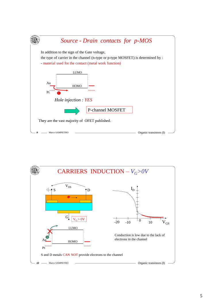
Source - Drain contacts for p-MOS
In addition to the sign of the Gate voltage,
the type of carrier in the channel (n-type or p-type MOSFET) is determined by :
- material used for the contact (metal work function)
They are the vast majority of OFET published.
P-channel MOSFET
HOMO
LUMO
+
Au
Pt
Hole injection : YES
10 Marco SAMPIETRO Organic transistors (I)
Conduction is low due to the lack of
electrons in the channel
S and D metals CAN NOT provide electrons to the channel
S D
G VG > 0V
+
ID
VGS 0 -20 -10 10
CARRIERS INDUCTION – VG>0V
VDS
HOMO
LUMO
Au
Pt
-
6
11 Marco SAMPIETRO Organic transistors (I)
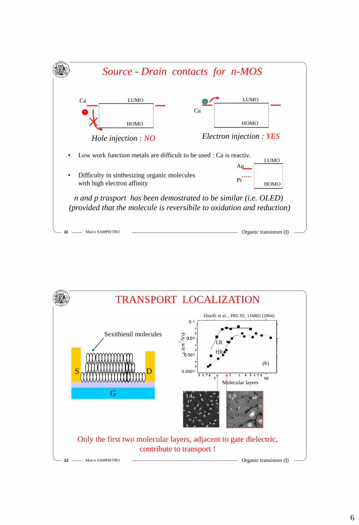
Source - Drain contacts for n-MOS
HOMO
LUMO
+
Ca
Hole injection : NO Electron injection : YES
HOMO
LUMO
Ca
-
• Low work function metals are difficult to be used : Ca is reactiv.
n and p trasport has been demostrated to be similar (i.e. OLED)
(provided that the molecule is reversibile to oxidation and reduction)
HOMO
LUMO Au
Pt • Difficulty in sinthesizing organic molecules
with high electron affinity
12 Marco SAMPIETRO Organic transistors (I)
TRASPORTO DI CARICA nei OFET TRANSPORT LOCALIZATION
Only the first two molecular layers, adjacent to gate dielectric,
contribute to transport !
Molecular layers
Dinelli et al. , PRL 92, 116802 (2004)
LR
HR
S D
G
Sexithienil molecules
7
13 Marco SAMPIETRO Organic transistors (I)
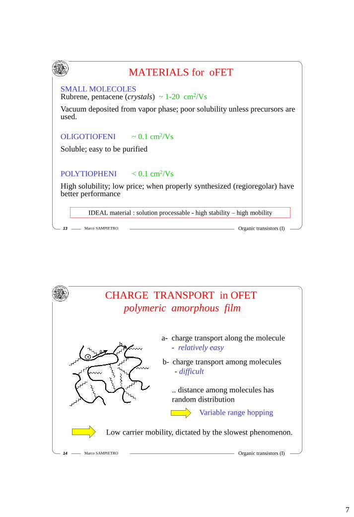
MATERIALS for oFET
SMALL MOLECOLES Rubrene, pentacene (crystals) ~ 1-20 cm2/Vs
Vacuum deposited from vapor phase; poor solubility unless precursors are used.
OLIGOTIOFENI ~ 0.1 cm2/Vs
Soluble; easy to be purified
POLYTIOPHENI < 0.1 cm2/Vs
High solubility; low price; when properly synthesized (regioregolar) have better performance
IDEAL material : solution processable - high stability – high mobility
14 Marco SAMPIETRO Organic transistors (I)
TRASPORTO DI CARICA nei OFET
a- charge transport along the molecule
- relatively easy
CHARGE TRANSPORT in OFET
polymeric amorphous film
Low carrier mobility, dictated by the slowest phenomenon.
.. distance among molecules has
random distribution
Variable range hopping
b- charge transport among molecules
- difficult
8
15 Marco SAMPIETRO Organic transistors (I)
Mobility increases as temperature
increases (phonon-mediated hopping
between localized states)
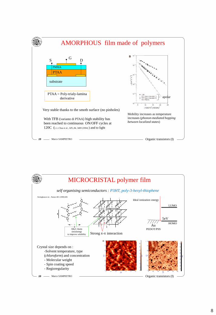
AMORPHOUS film made of polymers
PMMA
substrate
PTAA
G S D
PTAA = Poly-trialy-lamina
derivative
With TFB (variante di PTAA) high stability has
been reached to continuous ON/OFF cycles at
120C (L.L.Chua et al., APL,84, 3400 (2004) ) and to light
apolar
Very stable thanks to the smoth surface (no pinholes)
16 Marco SAMPIETRO Organic transistors (I)
self organising semiconductors : P3HT, poly-3-hexyl-thiophene
MICROCRISTAL polymer film
Alkyl chains
(insulating)
to improve solubility
LUMO
HOMO Au
PEDOT/PSS
5eV
Ideal ionization energy
Sirringhaus et al. , Nature 401 (1999) 685
Strong - interaction
Crystal size depends on :
-Solvent temperature, type
(chloroform) and concentration
- Molecular weight
- Spin coating speed
- Regioregularity

9
17 Marco SAMPIETRO Organic transistors (I)
FE=5.10-2 cm2/V.s FE=2.10-4 cm2/V.s
Mobility strongly
depends on the
orientation of the
molecule with respect
to the substrate …
MICROCRISTAL polymer film
Ong Synth.Met. 142 (2004) 49–52
310-2 cm2 / V.s
15.5Å
3.7Å
10-1cm2/Vs
Ong J. AM. CHEM. SOC. 2004, 126, 3378-3379
… and on the
molecule side
chains
and … (lesson II)
18 Marco SAMPIETRO Organic transistors (I)
Grain dimensions < 4nm
No precise gap
High density of localised states
Similarities with a-Si:H
Conduction is mainly hopping
between localized states
Deep levels due to
unsaturated bonds
(traps) within a
molecule
E
Higher disorder produces:
higher distances among molecoles,
higher variety of their interactions,
larger distribution of energetic levels,
larger gaussians.
10
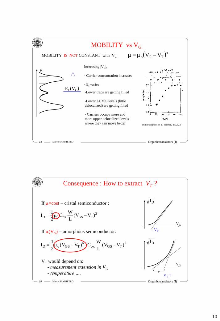
19 Marco SAMPIETRO Organic transistors (I)
MOBILITY IS NOT CONSTANT with VG
MOBILITY vs VG
Ef (VG)
Increasing |VG|,
- Carrier concentration increases
- Ef varies
-Lower traps are getting filled
-Lower LUMO levels (little
delocalized) are getting filled
- Carriers occupy more and
more upper delocalized levels
where they can move better
E
TGo VV
Dimitrakopulos et al. Science, 283,822
20 Marco SAMPIETRO Organic transistors (I)
Consequence : How to extract VT ?
If =cost – cristal semiconductor :
2TGS
'oxD )VV(
L
WC
2
1I
DI
VG
VT If (VG) – amorphous semiconductor:
2TGS
'oxTGSoD )VV(
L
WC)VV(
2
1I
VT would depend on:
- measurement extension in VG
- temperature ….
DI
VG
VT ?
11
21 Marco SAMPIETRO Organic transistors (I)
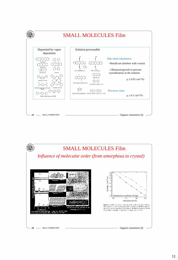
SMALL MOLECULES Film
Side chain substitution
Deposited by vapor
deposition
Solution processable
0.01 cm2/Vs
-Should not interfere with -stack
- Obtimized growth to prevent
crystallisation in the solution
Precursor route
0.1 cm2/Vs
22 Marco SAMPIETRO Organic transistors (I)
Influence of molecular order (from amorphous to crystal)
Simulazioni su rubrene (Troisi)
SMALL MOLECULES Film
12
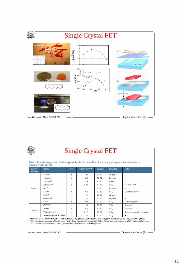
23 Marco SAMPIETRO Organic transistors (I)
Single Crystal FET
tetracene
antracene
24 Marco SAMPIETRO Organic transistors (I)
Single Crystal FET
13
25 Marco SAMPIETRO Organic transistors (I)
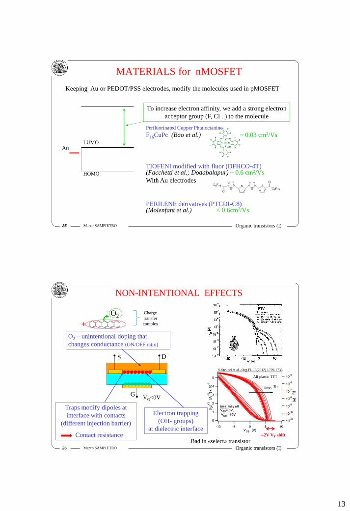
MATERIALS for nMOSFET
Keeping Au or PEDOT/PSS electrodes, modify the molecules used in pMOSFET
Perfluorinated Cupper Phtaloctanine
F16CuPc (Bao et al.) ~ 0.03 cm2/Vs
TIOFENI modified with fluor (DFHCO-4T) (Facchetti et al.; Dodabalapur) ~ 0.6 cm2/Vs
With Au electrodes
PERILENE derivatives (PTCDI-C8) (Molenfant et al.) < 0.6cm2/Vs
HOMO
LUMO Au
To increase electron affinity, we add a strong electron
acceptor group (F, Cl ..) to the molecule
26 Marco SAMPIETRO Organic transistors (I)
NON-INTENTIONAL EFFECTS
S D
G VG<0V
+ + + + + + + +
- - - - - - - - - -
O2 – unintentional doping that
changes conductance (ON/OFF ratio)
-
Traps modify dipoles at
interface with contacts
(different injection barrier)
Contact resistance
+
O2 Charge
transfer
complex
2V VT shift
S.Steudel et al., Org.El. 13(2012) 1729-1735
, 3h
All plastic TFT
Bad in «select» transistor
Electron trapping
(OH- groups)
at dielectric interface
14
27 Marco SAMPIETRO Organic transistors (I)
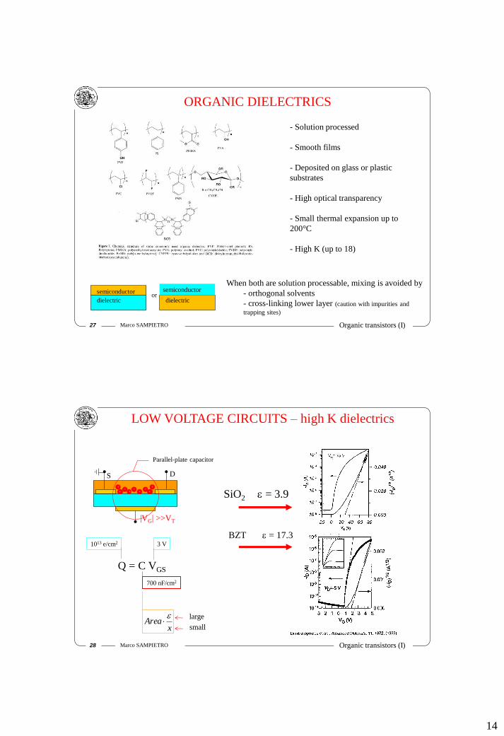
ORGANIC DIELECTRICS
- Solution processed
- Smooth films
- Deposited on glass or plastic
substrates
- High optical transparency
- Small thermal expansion up to
200°C
- High K (up to 18)
dielectric
semiconductor
When both are solution processable, mixing is avoided by
- orthogonal solvents
- cross-linking lower layer (caution with impurities and
trapping sites)
dielectric
semiconductor or
28 Marco SAMPIETRO Organic transistors (I)
LOW VOLTAGE CIRCUITS – high K dielectrics
Q = C VGS
1013 e/cm2
S D
|VG| >>VT
+ + + + + + +
+ +
Parallel-plate capacitor
SiO2 = 3.9
BZT = 17.3 3 V
700 nF/cm2
small xArea
large
15
29 Marco SAMPIETRO Organic transistors (I)
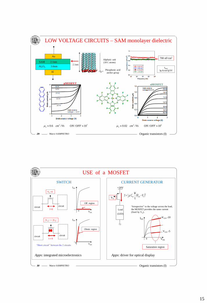
LOW VOLTAGE CIRCUITS – SAM monolayer dielectric
Au 700 nF/cm2
Al
Al2O3 3.6nm
SAM 2.1nm Aliphatic unit
(18 C atoms)
Phosphonic acid
anchor group
Ileak
3A/cm2@3V
2.1nm
pMOSFET nMOSFET
72 10//6.0 OFFONVscmn52 10//02.0 OFFONVscmn
30 Marco SAMPIETRO Organic transistors (I)
USE of a MOSFET
“Short circuit” between the 2 circuits
circuit I=0
VG=0
circuit
VDS
IDS
0
I 0
|VG| >> |VT|
+ + +
circuit circuit
VDS
IDS
0
Ohmic region
SWITCH
Off region
Apps: integrated microelectronics
“Irrespective” to the voltage across the load,
the MOSFET provides the same current
(fixed by VG).
Saturation region
VDS
IDS
0
VGS=-5
VGS=-10
VG
+20V
Load
(LED)
2'
21
TGSox VVL
WCI
CURRENT GENERATOR
Apps: driver for optical display
16
31 Marco SAMPIETRO Organic transistors (I)
Ion / Ioff RATIO
VDS
IDS
0
ION VGS=Valim ION
ION : “maximum” current drawn by the MOSFET
at VGS equal to the voltage supply.
2TmaxoxON VVL
WC
2
1I
Maximise Cox=/xox
(thin insulator and high )
IOFF IOFF nA
S D
G
VDS
VG=0V
+
Minimise thickness
Minimise intrinsic doping
L
WYpqVI pDSOFF
IOFF : undesired current tra S e D when
VG=0V
32 Marco SAMPIETRO Organic transistors (I)
TFT area vs mobility and feature size
2
Tgs
'
ox21
D )VV(L
WCI
Mobility (cm2/Vs)
Feature size 0.01 1
20 m W = 500 m
Area = 175x175 m2
W = 20 m
Area = 35x35 m2
5 m W = 125 m
Area = 45x45 m2
W = 5 m
Area = 9x9 m2
Data: Iled=2A, C’ox=700nF/cm2, Vgs-VT=5V
Size
17
33 Marco SAMPIETRO Organic transistors (I)
… and higher
mL
VV
Vscm
DS
n
2
3
/1.0 2
fT ~ 400 kHz
J.Am. Chem. Soc. 130, 4637 (2008)
Cyano-Perylene Tetracarboxylic Diimide
(PTCDI)
FREQUENCY of OPERATION 26 L
Vf DS
T
Current technology
mL
VV
Vscm
DS
n
20
3
/02.0 2
fT ~ 800 Hz
Reduction of channel length …
mL
VV
Vscm
DS
n
2
3
/02.0 2
fT ~ 80 kHz
34 Marco SAMPIETRO Organic transistors (I)
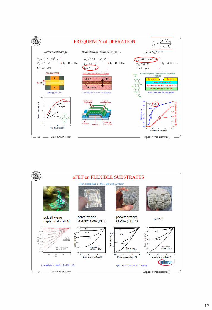
oFET on FLEXIBLE SUBSTRATES
From Hagen Klauk – MPI, Stuttgart, Germany
S.Steudel et al., Org.El. 13 (2012) 1729
Al2O3
dielectric
18
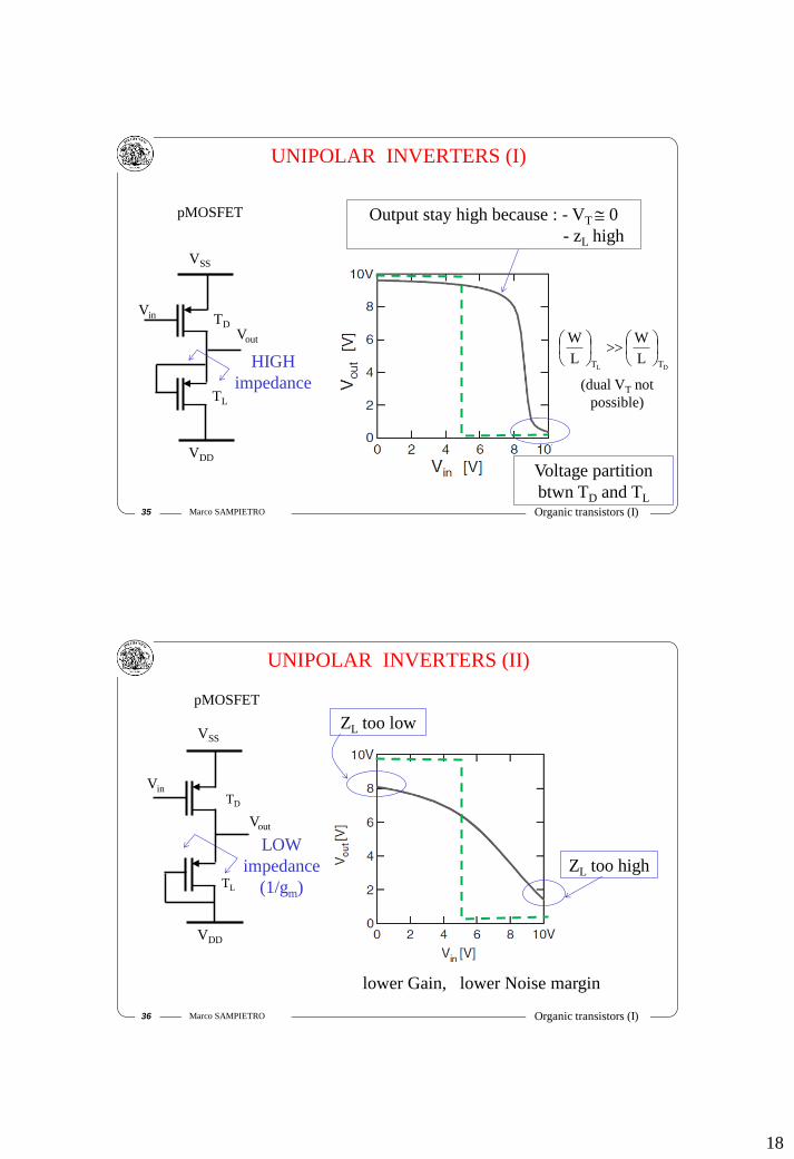
35 Marco SAMPIETRO Organic transistors (I)
UNIPOLAR INVERTERS (I)
pMOSFET
VSS
Vin
VDD
TD
TL
Vout
HIGH
impedance
Output stay high because : - VT 0
- zL high
Voltage partition
btwn TD and TL
DL TT L
W
L
W
(dual VT not
possible)
36 Marco SAMPIETRO Organic transistors (I)
UNIPOLAR INVERTERS (II)
pMOSFET
LOW
impedance
(1/gm)
ZL too low VSS
Vin
VDD
TD
TL
Vout
ZL too high
lower Gain, lower Noise margin
19
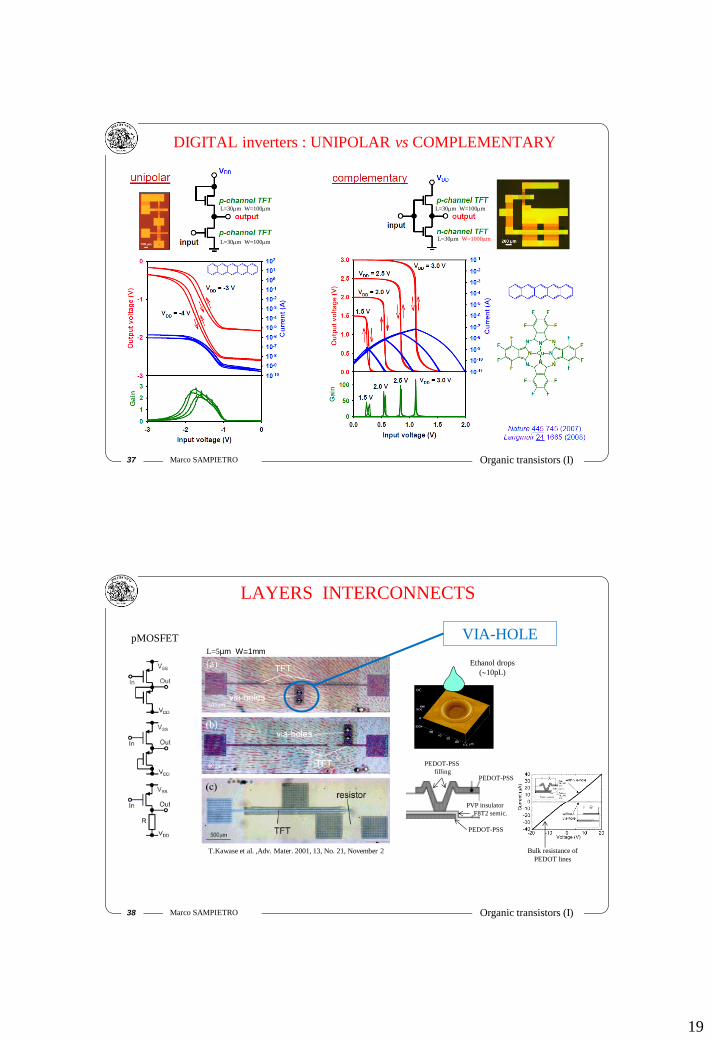
37 Marco SAMPIETRO Organic transistors (I)
DIGITAL inverters : UNIPOLAR vs COMPLEMENTARY
L=30m W=100m
L=30m W=100m
L=30m W=100m
L=30m W=1000m
38 Marco SAMPIETRO Organic transistors (I)
LAYERS INTERCONNECTS
T.Kawase et al. ,Adv. Mater. 2001, 13, No. 21, November 2
pMOSFET
Ethanol drops
(10pL)
VIA-HOLE
PEDOT-PSS
PEDOT-PSS
filling PEDOT-PSS
PVP insulator
F8T2 semic.
Bulk resistance of
PEDOT lines
L=5µm W1mm
20
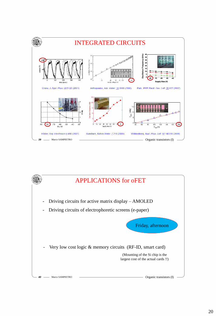
39 Marco SAMPIETRO Organic transistors (I)
TRASPORTO DI CARICA nei OFET INTEGRATED CIRCUITS
40 Marco SAMPIETRO Organic transistors (I)
TRASPORTO DI CARICA nei OFET
- Driving circuits for active matrix display – AMOLED
- Driving circuits of electrophoretic screens (e-paper)
APPLICATIONS for oFET
Friday, afternoon
(Mounting of the Si chip is the
largest cost of the actual cards !!)
- Very low cost logic & memory circuits (RF-ID, smart card)
21
41 Marco SAMPIETRO Organic transistors (I)
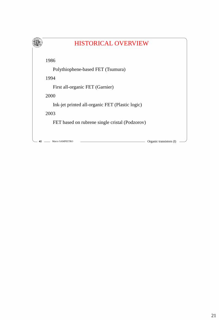
TRASPORTO DI CARICA nei OFET HISTORICAL OVERVIEW
1986
Polythiophene-based FET (Tsumura)
1994
First all-organic FET (Garnier)
2000
Ink-jet printed all-organic FET (Plastic logic)
2003
FET based on rubrene single cristal (Podzorov)