Embed Size (px)
Citation preview

OPTICAL PROPERTIES OF III-NITRIDE SEMICONDUCTORS AND
THE APPLICATIONS IN ALL-OPTICAL SWITCHING
By
Yueting Wan
M.Eng. (Telecommunications), Asian Institute of Technology, 1997 M.S. (Physics), University of Memphis, 2000
Submitted to the Department of Electrical Engineering and Computer Science and the Faculty of the Graduate School of the University of Kansas In partial fulfillment of the requirements for the degree of
Doctor of Philosophy
________________________
Chairperson
Committee members ________________________
________________________
________________________
________________________ Date defended: _____________________

ii
The Dissertation Committee for Yueting Wan certifies that this is the approved version of the following dissertation:
OPTICAL PROPERTIES OF III-NITRIDE SEMICONDUCTORS AND
THE APPLICATIONS IN ALL-OPTICAL SWITCHING Committee:
__________________________________ Chairperson
__________________________________
__________________________________
__________________________________
__________________________________
Date approved: _____________________

iii
To My Parents and Siblings

iv
ACKNOWLEDGEMENTS
I would like to express my gratitude to Dr. Rongqing Hui, my committee chair,
for his guidance throughout this research work and for his precious advice and
support during my graduate studies here at the University of Kansas. His
encouragement and full support led me to the success of this work. I have also been
able to learn a lot from him about being a better researcher. It was an absolute
pleasure working for him the past five years.
I would also like to thank other members of my committee, Dr. Christopher
Allen, Dr. Victor Frost, Dr. Hongxing Jiang and Dr. Karen Nordheden, for serving on
my dissertation committee and giving me invaluable suggestions through out my
research work. Also, I would like to express my thanks to the National Science
Foundation for providing the financial support for my research work.
Finally, I would like to thank my family and friends for their patience and
encouragement throughout the work of my dissertation. The support from them
makes this work successful.

v
ABSTRACT
The goal of this research was to build an N×N all-optical WDM switch, which
is indispensable for the next-generation of all-optical packet-switched networks. We
started from the basic concepts of telecommunication network architectures, optical
networks, WDM network elements and basic components in optical networks. We
focused on the principles and applications of optical couplers, Mach-Zehnder
Interferometers (MZI), arrayed waveguide gratings (AWG), and some switch
architectures and techniques that have helped in the design of the optical switch.
Based on the AWG principle, we derived a general design rule for
constructing an N-interleaved AWG (N-IAWG), and proposed a 1×N WDM switch
consisting of two N-IAWGs and a phase shifter array. We then simplified the
structure by using only one N-IAWG with total reflection implemented at the end of
each phase shifter. The simplified structure significantly reduced the device size and
relaxed the design tolerance. This suggests that it could be used as the fundamental
building block to construct non-blocking N×N all-optical WDM switches with Spanke
architecture.
The feasibility of the proposed optical switch depends on the refractive index
tuning in the phase shifter array, which can be realized through the carrier-induced
index tuning of semiconductors. We proposed to use III-nitride semiconductors due to

vi
their unique characteristics, and presented a theoretical study of carrier-induced
refractive index change in GaN in the infrared wavelength region. Calculations
verified that the magnitude of carrier-induced refractive index change is high enough
for the application to the proposed optical switch.
We then prepared various devices in GaN/AlGaN material and characterized
their optical properties in the 1550 nm wavelength region experimentally. We
measured the refractive indices and the impact of Al concentrations. We also
measured the birefringence of the GaN waveguides, which helped understand the
polarization effect in the devices and would help design polarization independent
optical waveguides. Among the devices we prepared, there was an eight-wavelength
AWG, which was the first AWG in GaN/AlGaN material. The performance of the
AWG agreed well with our design expectations and may be a foundation for the
application in optical switches.

vii
TABLE OF CONTENTS
1. Introduction……………………………………………………………………. 1
2. Optical Networking and Switching…………………………………………... 4
2.1. Introduction………………………………………………………….…… 4
2.2. Telecommunications Network Architecture……………………………... 4
2.3. Optical Networks………………………………………………………… 8
2.3.1. Multiplexing Techniques ………………………………….…... 8
2.3.2. Second-Generation Optical Networks…………………………. 10
2.4. WDM Network Elements………………………………………………... 12
2.5. Basic Components……………………………………………………….. 17
2.5.1. Couplers………………………………………………………… 17
2.5.2. Mach-Zehnder Interferometer………………………………….. 20
2.5.3. Arrayed Waveguide Grating…………………………………… 23
2.6. Optical Switches…………………………………………………………. 26
2.6.1. Large Optical Switch Architectures……………………………. 28
2.6.2. Optical Switch Technologies…………………………………... 31
2.7. WDM Optical Switches…………………………………………………. 36
2.7.1. Design of Passive Waveguide Devices………………………… 36
2.7.2. Design of Carrier Controlled Simple Waveguide Devices…….. 40
2.7.3. Design of Carrier Controlled AWG All-Optical Switch……….. 47
2.8. Design of All-Optical Switch Networks…………………………………. 52
2.9. Conclusion……………………………………………………………….. 53
3. Design of WDM Cross Connect Based on Interleaved AWG (IAWG) and a
Phase Shifter Array……………………………………………………………
54

viii
3.1. Introduction……………………………………………………………… 54
3.2. An Approach of an N × N All Optical Switch………………………….. 56
3.3. The Scheme of the 1 × N All-Optical Switch…………………………... 58
3.4. Design of the N-IAWG…………………………………………………. 59
3.4.1. Functionality of N-IAWG……………………………………… 59
3.4.2. From AWG to IAWG………………………………………….. 61
3.4.3. AWG Multiple-Beam Interference Condition…………………. 63
3.4.4. Vector Illustration of the AWG Multiple-Beam Interference
Condition……………………………………………………….
65
3.4.5. Additional Lengths to Arrayed Waveguides for Constructing
4-IAWG…………………………………………………………
66
3.4.6. General Design Rule of N-IAWG……………………………… 69
3.4.7. Output Port Arrangement………………………………………. 70
3.4.8. Comparison with Previous Results…………………………….. 71
3.4.9. Verification of Equal Vector Magnitudes in BZs of N-IAWG… 73
3.4.10. Verification of N-IAWG with Numerical Simulation…………. 79
3.4.11. Transfer function of an N-IAWG………………………………. 83
3.4.12. Extinction Ratio Versus the Interleaved Number N……………. 85
3.5. Realization of a 1 × N All Optical Switch………………………………. 86
3.5.1. The Transfer Function of a 1 × N All-Optical Switch………… 86
3.5.2. Switching Functionality Verification and Phase Change
Information……………………………………………………..
87
3.5.3. Simulation Verification ------An Example……………………... 90
3.5.4. The Scheme of Mirror 1 × N All-Optical Switch………………. 94
3.6. Conclusion……………………………………………………………….. 96

ix
4. Carrier Induced Refractive Index Changes in GaN/AlGaN
Semiconductors…………………………………………………………………
98
4.1. Introduction………………………………………………………………. 98
4.2. Carrier-Induced Refractive Index Change in Semiconductors…………... 100
4.2.1. Bandfilling……………………………………………………… 100
4.2.2. Bandgap Shrinkage…………………………………………….. 114
4.2.3. Free-Carrier Absorption………………………………………... 116
4.2.4. Combination of Effects………………………………………… 118
5. GaN Material Design and Experiments……………………………………… 123
5.1. Introduction………………………………………………………………. 123
5.2. Optical Waveguide Theory………………………………………………. 124
5.2.1. Symmetric Dielectric Slab Waveguides……………………….. 125
5.2.2. Asymmetric Dielectric Slab Waveguides……………………… 130
5.2.3. Rectangular Dielectric Waveguides……………………………. 131
5.3. Beam Propagation Method………………………………………………. 137
5.3.1. Finite Difference Method Analysis of Planar Optical
Waveguides……………………………………………………..
138
5.3.2. FDMBPM Analysis of Rectangular Waveguides……………… 140
5.3.3. Straight Waveguide Design with BPM Software……………… 141
5.4. Measurement Method and Experimental Setup…………………………. 152
5.4.1. Measurement Method Based On Febry-Perot (FP) Interference. 152
5.4.2. Experimental Setup……………………………………………. 154
5.5. Measurement of Refractive Indices in Infrared…………………………. 155
5.6. Measurement Results of the Single-Mode GaN/AlGaN Waveguides….. 157
5.6.1. Experimental Results: Power Loss in Waveguide Transmission. 157

x
5.6.2. Birefringence of GaN/AlGaN optical waveguides…………….. 159
5.7. Design of the Optical Couplers and the Mach-Zehnder Interferometer
Device with GaN/AlGaN…………………………………………………
166
5.7.1. Simulation Results of Couplers and Mach-Zehnder
Interferometer Device…………………………………………..
167
5.7.2. A Simple Example: Waveguide Coupler………………………. 169
5.8. The AWG Based on the GaN/AlGaN Heterostructures…………………. 170
5.8.1. Simulation Results of the Arrayed Waveguide Gratings………. 172
5.8.2. A Sample: A Fabricated Arrayed Waveguide Grating………… 174
5.9. The Thermal Stability of the Refractive Index…………………………... 177
6. Conclusions and Future Work………………………………………………... 182
6.1. Conclusions………………………………………………………………. 182
6.2. Future Work……………………………………………………………… 185
7. Bibliography…………………………………………………………………….. 188

xi
LIST OF FIGURES
Figure 2.1. An overview of a public fiber network architecture………………... 5
Figure 2.2. Different types of time division of multiplexing: (a) fixed, (b)
statistical…………………………………………………………….
7
Figure 2.3. Different multiplexing techniques for increasing the transmission
capacity on an optical fiber. (a) Electronic or optical time division
multiplexing and (b) wavelength division
multiplexing…………………………………………………………
9
Figure 2.4. A WDM wavelength-routing network, showing optical line
terminals (OLTs), optical add/drop multiplexers (OADMs), and
optical crossconnects (OXCs). The network provides lightpaths to
its users, which are typically IP routers or SONET
terminals……………………………………………………………..
11
Figure 2.5. Block diagram of an optical line terminal…………………………... 12
Figure 2.6. Illustrating the role of optical add/drop multiplexers……………….. 13
Figure 2.7. A fully tunable OADM……………………………………………... 14
Figure 2.8. An OXC is applied in the network………………………………….. 15
Figure 2.9. An optical core wavelength plane OXC……………………………. 16
Figure 2.10. A directional coupler………………………………………………... 17
Figure 2.11. A basic 2×2 Mach-Zehnder Interferometer…………………………. 20
Figure 2.12. Transfer functions of the basic 2×2 Mach-Zehnder Interferometer… 22
Figure 2.13. Illustration of an arrayed Waveguide Grating structure…………….. 25
Figure 2.14. Configuration of the star coupler…………………………………… 25
Figure 2.15. A 4 × 4 crossbar switch realized using 16 2 × 2 switches…………... 28

xii
Figure 2.16. A strict-sense nonblocking three-stage 1024 × 1024 Clos
architecture switch…………………………………………………..
29
Figure 2.17. A strict-sense nonblocking Spanke architecture n × n switch………. 30
Figure 2.18. An analog beam steering mirror…………………………………….. 32
Figure 2.19. An n × n switch built using two arrays of analog beam steering
MEMS mirrors………………………………………………………
33
Figure 2.20. Mach-Zehnder Interferometer As Thermo-Optical Switch…………. 35
Figure 2.21. Schematic diagram illustrating the operation of a wavelength
router: (a) Interconnectivity scheme (ai denotes the signal at input
port a with frequency i) and (b) Frequency response……………….
37
Figure 2.22. Three different ADM configurations: (a) Loop-back, (b) fold-back,
and (c) cascaded demux/mux………………………………………..
39
Figure 2.23. Schematic diagram of a tunable filter with a ladder-type structure… 41
Figure 2.24. (a) AWG Functioning As a Filter. (b) Electrode Controlled AWG
Filter…………………………………………………………………
44
Figure 2.25. Electrode Controlled AWG Filter, with different lengths of
electrodes……………………………………………………………
46
Figure 2.26. Schematic diagram of the interleave cross connect. The inset in the
lower left corner illustrates the Brillouin zones for star coupler 2….
48
Figure 2.27. Carrier Controlled Loop-Back Add-Drop Switch (a) Schematic
Diagram, (b) Corresponding Black Box…………………………….
51
Figure 2.28. 1 × N Wavelength Switch Network………………………………… 52
Figure 3.1. The scheme of 4×4 all-optical switch………………………………. 57
Figure 3.2. Schematic diagram of 1 × N all-optical switch……………………... 59
Figure 3.3. Schematic diagram of N-IAWG…………………………………….. 60

xiii
Figure 3.4. Diagram of output port distribution for an N-interleaved AWG. (a)
An N-interleaved AWG, where N = 4; (b) Close-up of the output
star coupler, where Ωi (i = -1, 0, 1, 2) denotes the new Brillouzin
zones of this 4-IAWG. These new BZs were split from the central
BZ of a conventional AWG before it was interleaved………………
64
Figure 3.5. (a) Diagram of output port distribution for a 5-interleaved AWG.
(b) Close-up of the output star coupler, where Ωi (i = -2, -1, 0, 1, 2)
denotes the new BZs of this 5-IAWG. These new BZs were split
from the central BZ of a conventional AWG before it was
interleaved…………………………………………………………...
74
Figure 3.6. (a) The changes of the signal vectors in BZ Ω1 when an AWG
changes to a 5-IAWG; (b) The changes of the signal vectors in BZ
Ω2 when an AWG changes to a 5-IAWG…………………………...
77
Figure 3.7. Verification of 4-IAWG. The output powers at its related four
output ports are exactly the same for each channel. (a) Central
channel with wavelength λ0 = 1550 nm, (b) Channel of wavelength
1549.2 nm, (c) Channel of wavelength 1549.6 nm, (d) Channel of
wavelength 1550.4 nm………………………………………………
81
Figure 3.8. Schematic diagram of 1×4 switch for single channel with
wavelength λ0……………………………………………………….
89
Figure 3.9. Simulation result of 1×4 switch for four wavelength channels with
wavelengths 1549.2 nm, 1549.6 nm, 1550.0 nm and 1550.4 nm
with a channel spacing of 0.4 nm. The 1550.0nm channel was
switched to output port 1, 1549.6nm channel to output 2, 1550.4nm
channel to output 3 and 1549.2nm channel to output 4……………..
91

xiv
Figure 3.10. Simulation result of 1×4 switch for four wavelength channels with
wavelengths 1549.2 nm, 1549.6 nm, 1550.0 nm and 1550.4 nm
with a channel spacing of 0.4 nm. The crosstalk between channels
is round –32 dB or less………………………………………………
92
Figure 3.11. Mirror scheme of 1 × N all-optical switch………………………….. 94
Figure 3.12. Simulation result of the mirror scheme of 1 × (N–1) all-optical
switch for N = 4……………………………………………………...
95
Figure 4.1. Energy band structure and Bandfilling effect for direct-gap
semiconductor. Absorption of a photon can occur only between
occupied valence band states and unoccupied conduction band
states…………………………………………………………………
101
Figure 4.2. The absorption coefficient versus photon energy for GaN layer
grown on sapphire. T = 293 K……………………………………….
107
Figure 4.3. The absorption coefficient versus photon energy for GaN layer
grown on sapphire. T = 10 K (Provided by Dr. Wei Shan)………….
109
Figure 4.4. Change in absorption due to electron-hole injection and the
resulting Bandfilling in GaN. Note: the vertical values are in
logarithm…………………………………………………………….
110
Figure 4.5. Change in refractive index due to Bandfilling effect of GaN.
N = P =3.0 ×10¹⁷, 1.0 ×10¹⁸, 3.0 ×10¹⁸, 1.0 ×1019 cm-3……………...
111
Figure 4.6. Index change versus signal wavelength due to Bandfilling effect in
GaN. Solid line: N = 7×1018cm-3, dashed line: N =3×1019cm-3,
dotted line: N = 6 ×1019 cm-3………………………………………...
112
Figure 4.7. Change of refractive index versus carrier density at 1550 nm for
GaN………………………………………………………………….
113

xv
Figure 4.8. Change of refractive index of GaN due to electron-hole injection
and the resulting band-gap shrinkage………………………………..
115
Figure 4.9. Index change versus signal wavelength due to bandgap shrinkage
effect of GaN. Solid line: N = 7×1018cm-3, dashed line: N
=3×1019cm-3, dotted line: N = 6 ×1019 cm-3…………………………
116
Figure 4.10. Index change versus signal wavelength due to plasma effect of
GaN. Solid line: N = 7×1018cm-3, dashed line: N =3×1019cm-3,
dotted line: N = 6 ×1019 cm-3………………………………………...
118
Figure 4.11. Predicted changes in refractive index of GaN from the combination
of three effects (the dashed line). N = P = 3 × 10¹⁹/cm-3……………
119
Figure 4.12. Overall index change versus wavelength calculated at three carrier
density levels: N =7×1018cm-3 (solid line), 3×1019cm-3 (dashed
line) and 6 ×10¹⁹, (dotted line)………………………………………
120
Figure 4.13. Index change versus carrier density calculated at 1550nm
wavelength…………………………………………………………..
121
Figure 5.1. A symmetric dielectric slab waveguide, where x-y is the
cross-section plane and z is the propagation direction………………
125
Figure 5.2. A graphical solution for determining α and kx for the modes in
symmetric dielectric slab waveguide………………………………..
127
Figure 5.3. An asymmetric dielectric slab waveguide…………………………... 129
Figure 5.4. A rectangular dielectric waveguide…………………………………. 131
Figure 5.5. Intensity patterns in a rectangular waveguide where w/d = 2, the
refractive index of the waveguide n1 = 1.5, and the background
medium has n0 = 1…………………………………………………..
133

xvi
Figure 5.6. (a) A rectangular dielectric waveguide to be solved using the
effective index method. (b) Solve the slab waveguide at each fixed
y and obtain an effective index profile neff(y). (c) Solve the slab
waveguide problem with the neff(y)……………………………….
135
Figure 5.7. The design of a layered rectangular waveguide with BeamPROP.
(a) Refractive index distribution. (b) The illustration of the cross
section of waveguide design. The refractive index is illustrated in
different colors. (c) Vertical cut of index profile of the rectangular
waveguide…………………………………………………………...
142
Figure 5.8. The mode calculation of a layered rectangular waveguide with
BeamPROP. (a) The basic mode. (b) The illustration of the cross
section of waveguide design. The refractive index is illustrated in
different colors. (c) Vertical cut of index profile of the rectangular
waveguide…………………………………………………………...
145
Figure 5.9. The cross section of the design of GaN single-mode waveguide…... 148
Figure 5.10. Simulation result of the designed GaN single-mode waveguide with
BeamPROP. (a) Single mode simulation verification and the
effective refractive index; (b) Radiation pattern versus exit angle;
(c) Refractive index characteristics along Y direction, at X = 0…….
150
Figure 5.11. Fiber-optical experimental setup……………………………………. 154
Figure 5.12. (a) Refractive indices of AlxGa1-xN versus wavelength for several
different Al molar fractions. (b) Sellmeier expansion coefficients
versus Al molar fractions……………………………………………
156
Figure 5.13. Measured optical transmission spectrum (solid point) and numerical
fitting using equation (2-13) (continuous line)……………………...
158

xvii
Figure 5.14. The wurtzite structure of GaN unit cell and the choice of
coordinates…………………………………………………………..
160
Figure 5.15. Waveguide sample. Waveguide differs by the angle θ……………... 160
Figure 5.16. Birefringence measurement experimental setup……………………. 161
Figure 5.17. Measured (solid dots) and calculated (continuous lines) optical
transfer function with the input optical field perpendicular (trace 1),
parallel (trace 3) and 450 from (trace 2) the crystal c-axis…………..
162
Figure 5.18. Measured birefringence versus waveguide orientation (solid
squares). The continuous line is a sinusoid fitting using, ∆n =
0.04275-0.00545cos(6θ), where θ is in degree……………………...
164
Figure 5.19. Simulation of a 3dB coupler………………………………………... 166
Figure 5.20. Simulation of M-Z Interferometer optical switch
controlled by carrier induced refractive index change………………
167
Figure 5.21. Microscopic images of a 2×2 GaN/AlGaN heterostructure optical
waveguide coupler (a) top view and (b) cross section at the output...
168
Figure 5.22. Measured output optical power vs the probe displacement in the
horizontal direction for a 2×2 GaN/AlGaN heterostructure optical
waveguide coupler. The input optical signal is launched at port 1….
169
Figure 5.23. (a) Arrayed waveguide grating configuration, (b) simulation output
result…………………………………………………………………
173
Figure 5.24. Microscope picture (a) and measured optical transfer function (b) of
an AWG-based WDM coupler with 2nm channel separation……….
176

xviii
Figure 5.25. Calculated temperature sensitivity of AlGaN refractive index, (a) as
a function of operation temperature for different Al concentration x
and, (b) as a function of Al concentration with a fixed operating
temperature at 25 0C…………………………………………………
180

xix
LIST OF TABLES
Table 3.1. Initial Vector Information for Constructing a 4-IAWG…………….. 65
Table 3.2. Vector Information of a Constructed 4-IAWG……………………... 67
Table 3.3. Multiple sets of additional waveguide lengths [λc] in the design of
an N-IAWG………………………………………………………….
70
Table 3.4. Comparisons between the distributions of additional waveguide
lengths [λc] in the design of IAWG…………………………………
72
Table 3.5. Initial Vector Information of Constructing a 5-IAWG……………... 76
Table 3.6. Extinction ratio (ER) versus the interleaved number N…………….. 86
Table 3.7. Phase changes (∆θ) needed in phase shifters for each output port
selection in 1×4 all-optical switch (λ = 1550 nm)…………………..
93
Table 3.8. Refractive index changes (∆n) needed in phase shifters with length
LP = 2 mm for each output port selection in 1×4 all-optical switch
(λ = 1550 nm)……………………………………………………….
93
Table 4.1. Values of Semiconductor Parameters (T = 300 K)…………………. 103
Table 4.2. Values of GaN Semiconductor Parameters (T = 300 K)…………… 108

1
1. Introduction
Internet traffic has been doubling every four to six months, and this trend
appears set to continue for a while [1]. This explosive growing of Internet traffic
requires the development of new technologies to fully utilize the wide bandwidth of
optical fibers (more than 50 THz [2]) and to manage the huge volume of data
information more efficiently. Although fiber-optic telecommunications has been
going through an enormous development since optical fibers have been applied in this
area, finding new optical materials, developing new fundamental optical devices and
designing new optical subsystems are still critical issues in constructing all-optical
telecommunications networks.
Unlike other communication technologies, optical technology offers a new
dimension, the color of light, to perform such network functions as multiplexing,
routing, and switching. Wavelength division multiplexing (WDM) techniques
effectively use the wavelength as an additional degree of freedom by concurrently
operating distinct portions of the 1.3- to 1.6-µm wavelength spectrum accessible
within the fiber network [3]. In WDM systems, WDM optical
multiplexers/demultiplexers, wavelength routers and optical amplifiers are the
fundamental devices.
So far, silica-based arrayed waveguide gratings (AWG) have been widely
used as WDM optical multiplexers and demultiplexers. However, due to its passive
nature, the lack of tunability limited its applications in dynamic wavelength routings.

2
The combination with mechanical optical switches partly solved this problem [4][5].
But it was still limited at the circuit switch level instead of the demanded packet
switch level, because of the slow response of the mechanical optical switch. InP is a
semiconductor material and the planar photonics integrated circuit (PIC) based on it
can be made tunable by carrier injection [6][7]. However, because of its high
refractive index and relatively small waveguide size, InP based PIC has its own
disadvantages such as, high scattering loss, high temperature sensitivity and high
coupling loss with optical fibers [8]. It thus became quite natural to find some other
semiconductor materials with lower refractive indices and lower temperature
sensitivity than InP to make the WDM devices.
III-nitride wide band gap semiconductors (GaN, AlGaN and InGaN) have
recently attracted intense attention [9][10] because of their unique characteristics.
Their wide bandgap and the hardness of the material make it possible to operate at
very high temperature and power levels and in harsher environments. The wide
bandgap also makes the materials highly transparent to the wavelength in the near
infrared region, which makes them excellent candidates for passive optical waveguide
devices for long wavelength optical communication. On one hand, the refractive
indices of III-nitride semiconductor materials (i.e. n = 2.34 for GaN) are lower than
those of InP (n = 3.5) [11], which makes III-nitrides better than InP to fit with optical
fibers. Additionally, the refractive index of III-nitrides can be varied and controlled
for example by alloying GaN with different percentages of InN and AlN. This is
essential for the design of integrated optical circuits. Furthermore, carrier injection in

3
heterostructures of InGaN/GaN and GaN/AlGaN can provide high-speed modulation
of refractive indices in waveguides, which can be utilized to make wavelength
selective optical routers based on fast switchable optical phased-arrayed (PHASAR)
devices.
The research will focus on the optical properties of III-nitride materials, the
design of the optical devices based on the materials and their applications in WDM
fiber-optic networks. The goal is to realize all-optical packet switches.
This thesis is divided into six chapters. After this introductory chapter, chapter
two presents a literature review. Chapter three outlines a complete theory about how
to design a 1 × N and N × N all optical switch. Chapter four shows physical properties
and calculated parameters of GaN semiconductor materials. In chapter five, we show
the results of the characterizations of the fabricated III-Nitride devices and our
experimental measurements of the samples. Some important discoveries are also
summarized in this chapter. Chapter six shows the conclusion and the future work
needed in this area.

4
2. Optical Networking and Switching
2.1. Introduction
In this chapter, we will review some basic concepts of telecommunication
system architectures, optical networks, WDM system elements and basic components
in optical networks. Then our discussion will be focused on the concepts and
structures of optical switches which are used in WDM technology. We will start by
reviewing the Micro-Electro-Mechanical System (MEMS), which is currently a very
popular technology in terms of its applications in the building of optical switches.
Then we will review optical switches for WDM applications, in which we will
discuss why WDM switches are different from conventional optical circuit switches
and how to build WDM optical switches from simple integrated guided-wave optical
devices. At the end, we will propose several unique designs of waveguide based
WDM switches.
2.2. Telecommunications Network Architecture
Optical fiber provides an excellent medium to transfer huge amounts of data
per second (nearly 50 Tb/s). It has low cost per bit, extremely low bit error rates, low
signal attenuation (0.25 dB/km around 1550nm), low signal distortion, low power
requirement, low material use, small space requirement, and higher level of security.
So far, fiber optic networks have been widely applied in telecommunications.

5
Figure 2.1 shows an overview of a typical public fiber network architecture
[1]. The network consists of a long-haul network and a metropolitan network. The
long-haul network has a number of nodes with a pair of fibers between each other. It
connects between cities and different regions that are usually separated by long
distances. In this example, the connection between nodes for the long-haul network is
in mesh format. However, ring topologies are also often deployed to provide
alternative paths of traffic in case some of the links fail. The metropolitan network
consists of a metropolitan interoffice network and a metropolitan access network. The
interoffice network can have a link topology similar to that of the long-haul network.
It connects groups of central offices within a city or region. The access network,
HEW LETTPACK ARD
Central Office
Home
Business
MetropolitanInteroffice network
MetropolitanAccess network
Long haulInterexchange network
Figure 2.1 An overview of a public fiber network architecture (after [1]).

6
which typically covers a range of a few kilometers, extends from a central office out
to individual businesses and homes.
In a network as shown in Fig.2.1, there is always a concern about how to
connect two different nodes to have information transmitted between them while the
quality-of-service is guaranteed. Based on how traffic is multiplexed and switched
inside the network, there are two fundamental types of underlying switch
infrastructures: circuit-switch and packet-switch. A circuit-switched network provides
the capability of switching circuit connections to its customers, in which a guaranteed
amount of bandwidth is allocated to each connection. Once the connection is setup,
the dedicated bandwidth for the customer is always available. The sum of the
bandwidth of all the circuits, or connections, on a link must be less than the link
bandwidth.
The problem with circuit switching is that it is not efficient in handling bursty
data traffic. A bursty stream requires a lot of bandwidth from the network when all
users are active and very little bandwidth when there is no demand. It is usually
characterized by an average bandwidth and a peak bandwidth, which correspond to
the long-term average and the short-term burst rates, respectively. In a circuit-
switched network, one has to reserve sufficient bandwidth to deal with the temporary
peak rate, while this bandwidth may be unused for most of the time.
To deal with the problem of transporting bursty data traffic efficiently, packet
switching was introduced in which the data stream is broken up into small packets of
data and transmitted independently. Packet switching uses a technique called

7
statistical multiplexing when multiplexing multiple bursty data streams together on a
link. Different types of time division multiplexing are shown in figure 2.2.
Since each data stream is bursty, it is probably unlikely that all the streams are
active at any given time. Therefore the bandwidth required on the link can be made
significantly smaller than that required when all streams were active simultaneously.
This is the advantage of a packet-switched scheme. However, there are certainly
disadvantages associated with packet-switched networks especially when a large
number of streams are active simultaneously and the required bandwidth exceeds the
available bandwidth on the link. However, this only requires more effort to be made
from the carriers to provide some guarantees on the quality of service they offer.
Mu
1
2
(a)
1 2 1 2 1 2
Mu
1
2
(b)
Figure 2.2 Different types of time division of multiplexing: (a) fixed, (b) statistical. (after [1])

8
2.3. Optical Networks
In additional to providing enormous capacities, an optical network also
provides a common infrastructure over which a variety of services can be delivered.
With optical fibers widely deployed and the evolution of telecommunication networks,
optical networks have been evolved from the first generation, where optics was
essentially used for transmission and simply to provide capacity, to the second
generation, where some of the routing, switching, and intelligence is moving from the
electronics domain into the optical layer. Before we describe the second-generation
optical networks, let’s look at the multiplexing techniques utilized in current optical
networks.
2.3.1 Multiplexing Techniques
Multiplexing makes it possible to transmit data at higher rates and thus much
more economical. It is more convenient for many reasons to transmit high speed data
over a single fiber than to transmit lower data rates over multiple fibers. There are
fundamentally two ways of traffic multiplexing as shown in figure 2.3, which are
time division multiplexing (TDM) and wavelength division multiplexing (WDM). By
utilizing higher-speed electronics, TDM increases the bit rate by interleaving lower-
speed data streams to obtain the higher-speed stream at the transmission bit rate. To
achieve even higher bit rates with TDM technology, researchers are working on
methods to perform the multiplexing and demultiplexing all-optically. This approach
is known as optical time division multiplexing (OTDM). On the other hand, WDM is
essentially the same as frequency division multiplexing (FDM) in wireless systems. It

9
transmits data simultaneously at multiple carrier wavelengths over a fiber. Under first
order approximation, there is no crosstalk between these wavelengths as long as they
do not overlap with each other in the frequency domain. WDM has been widely
deployed in long-haul networks, and now is being deployed in metro and regional
access networks. [12].
1
2
N
...
B b/s
NB b/s
TDM or OTDM mux
(a)
1
2
N
...
B b/s
WDM mux
(b)
1λ
2λ
Nλ
1
2
N
...
B b/s
1λ
2λ
Nλ
Figure 2.3 Different multiplexing techniques for increasing the transmission capacity on an optical fiber. (a) Electronic or optical time division multiplexing
and (b) wavelength division multiplexing. (after [1])

10
WDM and TDM both provide ways to increase the transmission capacity and
are complementary to each other. Therefore networks today use a combination of
TDM and WDM.
2.3.2 Second-Generation Optical Networks
The architecture of a second-generation optical network is shown in figure 2.4.
This is a wavelength-routing network. The signals are transmitted from the source to
the destination through light paths provided by the network. The light paths are
optical connections from a source node to a destination node over a wavelength on
each intermediate link. The wavelength being routed on the light path can be
converted from one to another. The same wavelength can be used among different
light paths in a wavelength routing network as long as the light paths do not share any
common link. This means the wavelength can be reused spatially in different parts of
the network.
Fundamental building blocks of this second-generation optical network
include optical line terminals (OLTs), optical add/drop multiplexers (OADMs), and
optical cross-connects (OXCs), as shown in figure 2.4. An OLT multiplexes multiple
wavelengths into a single fiber and demultiplexes a set of wavelengths on a single
fiber into separate fibers. An OADM takes in signals of multiple wavelengths and
selectively drops some of these wavelengths or adds some other wavelengths locally
while letting others pass through. An OXC essentially performs a similar function in
routing that switches wavelengths from one input port to another but at much larger
sizes with the number of ports ranging from a few tens to thousands. Compared with
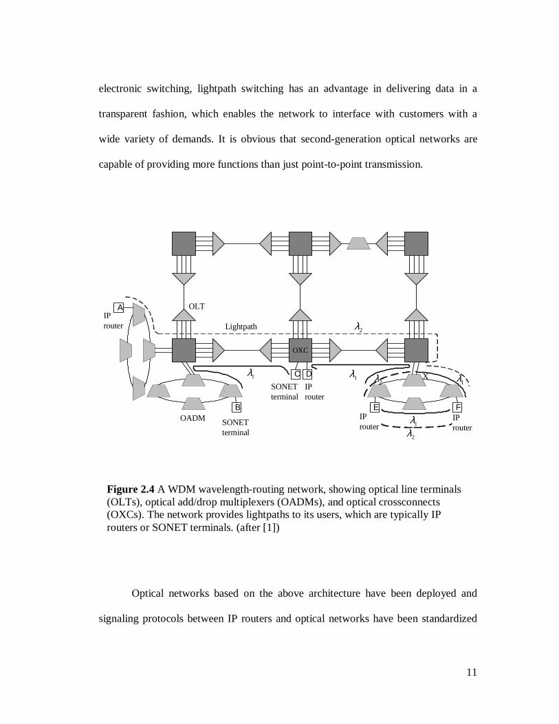
11
electronic switching, lightpath switching has an advantage in delivering data in a
transparent fashion, which enables the network to interface with customers with a
wide variety of demands. It is obvious that second-generation optical networks are
capable of providing more functions than just point-to-point transmission.
Optical networks based on the above architecture have been deployed and
signaling protocols between IP routers and optical networks have been standardized
OXC
OLT
Lightpath
A
DC
B FE
SONETterminal
IProuter
SONETterminal
IProuter
IProuter
IProuter
OADM
1λ1λ
1λ
1λ
2λ
2λ
2λ
X
Figure 2.4 A WDM wavelength-routing network, showing optical line terminals (OLTs), optical add/drop multiplexers (OADMs), and optical crossconnects (OXCs). The network provides lightpaths to its users, which are typically IP routers or SONET terminals. (after [1])

12
[13]. OLTs have been widely deployed for point-to-point applications. They can be
shared by all the optical network units (ONUs) to reduce the number of expensive
DWDM transceivers [14]. OADMs that support different data rates with same
bandwidth efficiency are developed [15] and are now used in long-haul and metro
networks [1][16][17][18]. OXCs were deployed primarily in long-haul networks
because of their high capacity requirement.
2.4. WDM Network Elements
As we mentioned above, OLT, OADM and OXC are three important elements
in optical networks. The users of the network are connected to these elements. Now
let’s have a brief overview of these three important elements.
Figure 2.5 Block diagram of an optical line terminal. (after [1])
Mux/demux
O/E/O
O/E/O
IP router
SONET
SONETTransmitter
Receiver
TransponderNon ITUλ
Non ITUλ
ITU 1λ
3λITU
ITU 2λ 1λ 2λ 3λ
OSCλOSCλ
Optical line terminal

13
Figure 2.5 shows a block diagram of an OLT [1]. An OLT is used at either
end of a point-to-point link to multiplex and demultiplex wavelengths. From the
figure, we can see that the signal coming out of a transponder is multiplexed with
other signals of different wavelengths onto a fiber. In the opposite direction, the
demultiplexer extracts the individual wavelengths and sends them either to the
transponder or to the client directly. A transponder adapts the signal from a client into
a signal suitable for use inside the optical network. Likewise, in the reverse direction,
it adapts the signal from the optical network into a signal suitable for the client. From
the figure, we can see that the OLT also terminates an optical supervisory channel
(OSC), which is carried on a separate wavelength λOSC, which is different from the
wavelengths carrying the actual traffic. From the description above, we can see that
the basic components in an OLT structure are the multiplexer and the demultiplexer,
which can be made by arrayed waveguide gratings (AWG), dielectric thin-film filters
and fiber Bragg gratings.
Optical passthrough
Node A Node CNode B
Add/Drop
OADM
Figure 2.6 Illustrating the role of optical add/drop multiplexers. (after [1])

14
Figure 2.6 illustrates the role of an OADM. In this example, a wavelength-
routing network is used. Nodes A and C are each deployed with an OLT and node B
is deployed with an OADM. The OADM drops one of the four wavelengths to a local
terminal and passes through three other remaining wavelengths. This is a cost-
effective solution for wavelength add/drop realization. Basic components in node B
are, again, a multiplexer and a demultiplexer.
Figure 2.7 shows an ideal reconfigurable OADM architecture. The
architecture is flexible and fully tunable regarding the channels being added or being
dropped while still maintaining a low fixed loss. The basic components used in this
structure are again a multiplexer and a demultiplexer, but in addition, an optical
switch is required for dynamic wavelength routing.
Demux MuxOptical switch
1λ
2λ
Nλ
...R
RT
T R
RT
T Tunable transponders
...1λ 2λ Nλ, , , ...1λ 2λ Nλ, , ,
Figure 2.7 A fully tunable OADM. (after [1])

15
OADMs are useful network elements to handle simple network topologies.
For more complex mesh topologies with large traffic and a large number of
wavelengths, OXCs are required. OXCs also help realize reconfigurable optical
networks in which lightpaths can be set up or terminated as needed without having to
distribute them beforehand. Figure 2.8 shows an OXC applied in the network. It
terminates some fiber links, each usually carrying a large number of wavelengths and
also passes other wavelengths through to other nodes. OXCs enable true mesh
networks to be deployed. There are different versions of OXCs. But ideally, it should
be able to provide lightpaths in a large network in an automated manner; it should be
an intelligent network element that can detect failures in the network and rapidly
reroute lightpaths around the failure; it should be bit rate transparent so that it can
switch signals with arbitrary bit rates and frame formats, etc.
OXC
OLT
IP SONNETSDH
ATM
Figure 2.8 An OXC is applied in the network. (after [1])

16
There is always a switch core in an OXC. The switching can be done either
electrically or optically. It is certainly preferred to have it done all-optically since all-
optical switches are more scalable in capacity, data rate transparent and it is not
necessary to groom traffic. Figure 2.9 shows an optical core wavelength plane OXC,
consisting of a plane of optical switches. The signals coming in from different fibers
are first demultiplexed and then sent to the optical switches according to their
wavelengths. Each optical switch switches signals with a specific wavelength. After
the signals are switched, they are multiplexed back together by multiplexers. The
configuration in figure 2.9 also shows the add/drop terminals for some channels.
Local add
OLT
Opticalswitch
1λ
Opticalswitch
2λ
Opticalswitch
3λ
Opticalswitch
4λOXC
OLT
1λ2λ 3λ 4λ1λ
2λ 3λ 4λ
Local drop
... ...
Figure 2.9 An optical core wavelength plane OXC. (after [1])

17
2.5. Basic Components
In the above section, we see that multiplexing, demultiplexing and optical
switching are indispensable functions in all-optical networks. Now we will present
some basic components that are used to realize all these functions.
2.5.1 Couplers
A directional coupler is used to combine or split signals in an optical network.
Figure 2.10 shows a 2 × 2 coupler consisting of two input ports and two output ports.
The power from one input port, P0 or P3, can be split into two output ports P1, and P2.
A quantitative analysis of this coupling phenomenon can be found in [19]. A
general form can be obtained for the relationship between the electric fields at the
output side, 1E and 2E , and the electric fields at the input sides, 0E and 3E [1].
Figure 2.10 A directional coupler.
Input powerThroughputpower
Coupledpower
(coupling length)l
Fibers or waveguides
0P 1P
2P3P
1
2
0
3

18
01
32
( )( ) cos( ) sin( )
( )( ) sin( ) cos( )j l E fE f l j l
eE fE f i l l
β κ κκ κ
− =
(2.1)
where l is the coupling length as shown in figure 2.10, β is the propagation constant
in each of the two waveguides of the directional coupler, κ is coupling coefficient and
is a function of the width of waveguides, the refractive indices of the waveguide core
and the substrate, and the proximity of the two waveguides.
A directional coupler is often used with only one active input, say input 0 as in
figure 2.10, although it has two input ports and two output ports. In this case, we can
get the power transfer function of the coupler from equation (2.1) by setting E3 = 0
2
01
202
( ) cos ( )
( ) sin ( )
T f l
T f l
κκ
=
(2.2)
Here, ( )ijT f represents the power transfer function from input i to output j and is
defined by2 2
( ) ( ) / ( )ij j iT f E f E f= . From equation (2.2), we can see that the
directional coupler is a 3-dB coupler when the coupling length l satisfies
(2 1) / 4l kκ π= + , where k is a nonnegative integer.
Below are some of the basic specifications of directional couplers [3].
Splitting ratio or coupling ratio:
00
21
2 100 ratio Splitting ×
+=
PP
P (2.3)
The two basic loss terms in a coupler are excess loss and insertion loss. The
excess loss is defined as the ratio of the input power to the total output power. Thus,
in decibels, the excess loss for a 2 × 2 coupler is

19
+=
21
0log 10 loss ExcessPP
P (2.4)
The insertion loss refers to the loss for a particular port-to-port path. For example, for
the path from input i to output j, we have, in decibels,
Insertion loss 10log i
j
P
P
=
(2.5)
Another performance parameter is crosstalk, which measures the degree of isolation
between the input power at one input port and the optical power scattered or reflected
back into the other input port.
A coupler may have many applications in an optical network. It can be either
wavelength selective or wavelength independent. For wavelength independent
couplers, one of the common uses is to split optical power. They can also be used to
tap off a small portion of the power from a system for monitoring purposes. For
wavelength dependent couplers, they are widely used to combine signals with
different wavelengths into a single output port or to separate the two signals coming
in on a common fiber to different output ports, fulfilling the functions of multiplexing
and demultiplexing. One thing should be mentioned when the coupler is used as a 3-
dB coupler. Although the electric fields at the two output ports have the same
magnitude, they have a relative phase shift of π/2. This characteristic plays a crucial
role in the design of devices like Mach-Zehnder Interferometer.

20
2.5.2 Mach-Zehnder Interferometer
Combining two 3-dB couplers together forms a Mach-Zehnder Interferometer
(MZI) as shown in figure 2.11. The device can be made either by fiber or by planar
waveguides, the latter is more rigid compared to fiber and therefore more stable.
Throughout this dissertation, we will only discuss waveguide-based MZIs.
The transfer function of the MZI shown in figure 2.11 can be obtained based
on the general relationship of a coupler as shown in equation (2.1). Since we are only
interested in the relative phase relationships for the transfer function, we can ignore
the common phase shift e-iβl at the right hand side of equation (2.1). For a 3-dB
coupler, the propagation matrix is
coupler
cos( ) sin( ) 11
sin( ) cos( ) 12
l j l jM
j l l j
κ κκ κ
= =
(2.6)
Figure 2.11 A basic 2×2 Mach-Zehnder Interferometer.
Pin, 0
Pout, 2
Pout, 11
2
λ0
3
n1
n2
L
Phase
shifter
l l
3-dB
Splitter
3-dB
Combiner
L+∆L

21
As for the central region in figure 2.11, we can see that the phase difference
caused by the two waveguides in that region can be expressed as
1 22 2( )
n nL L L
π πφλ λ
∆ = − + ∆ (2.7)
The phase difference can arise either from a different path length (∆L) or from a
difference of refractive indices (n1 ≠ n2). When n1 = n2 = neff, we have
k Lφ∆ = − ∆ (2.8)
where 2 /effk nπ λ= , so the propagation matrix for the phase shifter is
exp( / 2) 0
0 exp( / 2)
jk LM
jk Lφ∆
∆ = − ∆
(2.9)
The relationship between the electric fields at the output side, out,1E and out,2E , and the
electric fields at the input sides of the MZI, in,0E and in,3E is
out,1 in,0
out,2 in,3
E EC M
E E
=
i (2.10)
where C is a phase constant, which has 1C = , and M is the overall propagation
matrix of the MZI, which is expressed as
coupler coupler
sin( / 2) cos( / 2)
cos( / 2) sin( / 2)
k L k LM M M M j
k L k Lφ∆
∆ ∆ = = ∆ − ∆
i i (2.11)
From equations (2.10) and (2.11), we can get the output powers in the case of single
input (at 0 input port) as
* 2out,1 out,1 out,1 in,1sin ( / 2)P E E k L P= = ∆ (2.12)
* 2out,2 out,2 out,2 in,1cos ( / 2)P E E k L P= = ∆ (2.13)

22
So the transfer function of MZI for single power input at port 0 and two output ports
at port 1 and port 2 can be expressed as
201
202
( ) sin ( / )
( ) cos ( / )eff
eff
T n L
T n L
λ π λλ π λ
∆ = ∆
(2.14)
where neff is the effective refractive index in the waveguide, λ is the wavelength of the
input signal, ∆L is the difference between the lengths of the two arms in MZI as
shown in figure 2.11. This transfer function of equation (2.14) can be depicted in
figure 2.12. We see that wavelength λ1 output from port 1 and λ2 output from port 2.
Different wavelength signals go to different output ports. From equation (2.14), we
can see that switch functionality of the MZI can be realized if we can control or adjust
∆L.
It should be noted that figure 2.12 is based on n1 = n2, which means the two
arms in the central region of the MZI have the same effective refractive index and the
Figure 2.12 Transfer functions of the basic 2×2 Mach-Zehnder Interferometer
T
λ
State 1
State 2
λ1 λ2

23
phase difference between the two arms is expressed in equation (2.8). When n1 is not
equal to n2, the result would be different. From equation (2.7), we have
222 nLn L
ππφλ λ
∆ = − ∆ − ∆ (2.15)
where 2 1n n n∆ = − . The propagation matrix of the central region has the general form
as
exp( / 2) 0
0 exp( / 2)
jk LM
jk Lφ∆
∆ = − ∆
(2.16)
Based on equation (2.16), we get the general propagation matrix of the whole MZI as
coupler coupler
sin( / 2) cos( / 2)
cos( / 2) sin( / 2)M M M M jφ
φ φφ φ∆
− ∆ ∆ = = ∆ ∆
i i (2.17)
So the transfer function of MZI for single power input at port 0 and two outputs at
ports 1 and 2 can be expressed as
201
202
( ) sin ( / 2)
( ) cos ( / 2)
T
T
λ φλ φ
∆= ∆
(2.18)
From equation (2.15), we can see that we can change either ∆n or ∆L or both to have
different phase difference, ∆φ, between the two arms in the central region of the MZI.
From equation (2.18), we see that the output at each output port will be different for
each wavelength. This is the basis for our design of an all-optical switch based on the
interleaved arrayed waveguide gratings, which will be discussed in Chapter 3.
2.5.3 Arrayed Waveguide Grating
An arrayed-waveguide-grating (AWG) is typically used in WDM optical
systems as a frequency domain multiplexer, demultiplexer, or a wavelength router.
24
The wavelength selectivity of an AWG is based on multi-beam interference. Unlike a
conventional transmission or reflection grating, an AWG is composed of integrated
waveguides deposited on a planar substrate, which is commonly referred to as planar
lightwave circuit (PLC). As shown in Figure 2.13, the basic design of an AWG
consists of input and output waveguides, two star couplers and an array of
waveguides between the two star couplers. The array is composed in such a way that
any two adjacent waveguides have the same optical path difference, which satisfies
the constructive interference condition for the central wavelength λ0 of the signal.
The interference condition for the output signal also depends on the design of the star
couplers. For the star coupler, as schematically shown in figure 2.14, the input and the
output waveguides are positioned at the opposite side of a Rowland sphere with a
radius of Lf/2, where Lf is the focus length of the sphere. In an AWG operation, the
optical signal is first distributed into all the arrayed waveguides through the input star
coupler. After passing through the arrayed waveguides, the signal is diffracted into
the output star coupler where each wavelength component of the signal is added up
constructively at the appropriate output waveguide. The phase condition of this
constructive interference is determined by the following equation [20]:
λθ mdnLn osc =+∆⋅ sin (2.19)
where θo =j ⋅∆x/Lf is the diffraction angle in the output star coupler, ∆x is the
separation between adjacent output waveguides, j indicates the particular output
waveguide number, ∆L is the length difference between two adjacent waveguides in
the waveguide array, ns and nc are the effective refractive indices in the star coupler

25
and waveguides respectively, m is the diffraction order of the grating and an integer,
and λ is the wavelength.
Figure 2.13 Illustration of an Arrayed Waveguide Grating structure.
N
2
1
M
2
1 Input
Star coupler
Output
Star coupler
Waveguide array
Figure 2.14 Configuration of the star coupler.
Output w
aveguides
Wav
egui
de a
rray
d ∆ xL f
θ0
Rowland sphere
L f /2

26
Obviously, from equation (2.19), the constructive interference wavelength at
the central output waveguide λ0 is
m
Lnc ∆⋅=0λ (2.20)
On the other hand, also from equation (2.19), we can easily get the angular
dispersion with respect to wavelength λ, in the vicinity of θ0 = 0, as
c
g
s n
n
dn
m
d
d −=λθ
(2.21)
where ng is the group index that is defined as
λ
λd
dnnn c
cg −= (2.22)
Based on equation (2.21), the wavelength separation between two adjacent output
waveguides can be found as:
g
s
fg
cs
ff n
n
L
d
L
x
n
n
m
dn
L
x
d
d
L
x
∆∆=∆=
∆=∆−
0
1
0 λλθλ (2.23)
Since AWG is based on multi-beam interference, the spectral resolution of the
output signal is primarily determined by the number of the arrayed waveguides
between the two star couplers. A larger number of waveguides provides better
spectral resolution.
2.6. Optical Switches
From figure 2.7 and figure 2.9, we can see that OADMs and OXCs are
essentially optical switches in a general sense. Optical networks rely heavily on the

27
functionalities of all kinds of optical switches. Different applications in an optical
network require different switch times and numbers of switch ports. The switching
applications in an optical network include provisioning, protection switching, packet
switching and external modulation [1]. The required switch times range from
milliseconds to picoseconds. The number of switch ports may vary from two ports to
several hundreds to thousands of ports.
In addition to the switching time and number of ports, there are other
important parameters to be considered for optical switches. Those parameters include
extinction ratio, insertion loss, crosstalk, and polarization-dependent loss (PDL). The
extinction ratio is the ratio of the output power in the “on” state to the output power in
the “off” state. The insertion loss is the power lost because of the presence of the
switch. The crosstalk is the ratio of the power at the output port from the desired input
to the power at the same output port from all the other inputs. PDL is due to the loss
in some components depending on the polarization state of the input signal.
For large optical switches, the considerations should include the number of
switch elements required, loss uniformity, the number of waveguide crossovers and
blocking characteristics, etc. Large switches consist of multiple switch elements and
the number of the elements is an important factor that determines the cost and the
complexity of the switch. It is also desired to achieve uniform loss for different input
port and output port combinations in an optical switch. For integrated optical switches
using planar lightwave circuits, the connections between components must be made
in a single layer by means of waveguides and this will cause crossovers between

28
waveguides in some architectures, which causes power loss and crosstalk. Less
waveguide crossovers ensure better performance for an optical switch. As for the
definition of blocking or nonblocking of a switch, the switch is said to be
nonblocking if any unused input port can be connected to any unused output port.
Otherwise, the switch is blocking.
2.6.1 Large Optical Switch Architectures
2.6.1.1 Crossbar
Outputs
1
1
2
3
4
2 3 4
Inp
uts
Figure 2.15 A 4 × 4 crossbar switch realized using 16 2 × 2 switches. (after [1])

29
There are several large optical switch architectures proposed so far. The basic
one is called Crossbar. The crossbar architecture consists of a group of 2 × 2 switches
and is, in general, nonblocking. An n × n crossbar requires n2 2 × 2 switches. The
shortest path length is 1 and the longest path length is 2n – 1 in this architecture. This
large path length difference is one of the main drawbacks of this architecture since the
loss distribution will not be uniform. Figure 2.15 shows a 4 × 4 crossbar switch,
which uses 16 2 × 2 switches. The settings of the 2 × 2 switches for the connection
from input port 1 to output port 3 is shown in the figure. As we can see, the switch
can be fabricated without any crossovers between waveguides.
32 x 321
32
32 x 3232 x 32
32 x 64
32 x 64
32 x 64
32 x 64
32 x 64
32 x 64
...
...
... ...
...
...33
64
993
1024
1
32
33
64
993
1024
Inp
uts
Out
puts
Figure 2.16 A strict-sense nonblocking three-stage 1024 × 1024 Clos architecture switch. (after [1])

30
2.6.1.2 Clos
The second optical switch architecture introduced here is called Clos, which
provides a strict-sense nonblocking switch and is widely used in practice to build
large port count switches. Figure 2.16 shows a three-stage 1024-port Clos switch. The
architecture has loss uniformity between different input-output combinations and the
number of required switch elements is significantly reduced compared to the crossbar
architecture.
1 x n
n x 1
n x 1
n x 1
1 x n
1 x n
1
2
n
1
2
n
Inp
uts
Out
put
s
Figure 2.17 A strict-sense nonblocking Spanke architecture n × n switch. (after [1])

31
2.6.1.3 Spanke
Figure 2.17 shows another switch architecture which is called Spanke. The
Spanke architecture is very popular for building large switches. It can be seen from
the figure that an n × n switch consists of n 1 × n switches at the input side and n n ×
1 switches at the output side. This is also a strict-sense nonblocking architecture.
Instead of counting the number of 2 × 2 switches, a 1 × n switch or an n × 1 switch
can be made from a single switch unit, which reduces the cost significantly. Also it is
obvious that all connections only pass through two switch elements, which provides
much lower insertion loss than the multistage designs. Moreover, the optical path
length between any two-switch combinations can be made exactly the same so that
the loss uniformity can be realized.
Besides the architectures mentioned above, there are other switch
architectures such as Beneš and Spanke- Beneš. These architectures both have their
unique advantages and disadvantages. More details can be found from [1].
2.6.2 Optical Switch Technologies
There are many different technologies to realize optical switches, such as Bulk
Mechanical Switches, Micro-Electro-Mechanical System (MEMS) Switches,
Thermo-Optic Silica Switches, Bubble-Based Waveguide Switches, Liquid Crystal
Switches, Electro-Optic Switches, and Semiconductor Optical Amplifier Switches,
etc [1]. Here we will particularly introduce the MEMS since this type of switch is
very popular and still developing. Also, MEMS are widely used in current optical
communication systems. Then we will briefly introduce the Thermo-Optic Switch

32
since it will easily lead us to the switch mechanism and architecture proposed in this
dissertation.
2.6.2.1 Micro-Electro-Mechanical System (MEMS) Switches
Micro-Electro-Mechanical Systems (MEMS) is the integration of mechanical
elements, sensors, actuators, and electronics on a common silicon substrate through
micro-fabrication technology [21]. In the context of optical switches, MEMS usually
refers to miniature movable mirrors fabricated in silicon, with dimensions ranging
from a few hundred micrometers to a few millimeters [1]. By using standard
semiconductor manufacturing processes, arrays of micro mirrors can be made on a
single silicon wafer. These mirrors can be deflected to face different directions by
using techniques such as electromagnetic, electrostatic, or piezoelectric methods.
Mirror
Flexure
Figure 2.18 An analog beam steering mirror. (after [1])

33
There are many different mirror structures that can be used. The simplest
mirror structure is a 2D mirror, which can deflect between two positions. However
3D mirrors are more flexible, but fabrication is more complicated. Figure 2.18 shows
a 3D mirror structure. By rotating the mirror on two distinct axes (flexures), the
mirror can be turned to face any desired direction. This characteristic can be used to
realize 1 × n switch function.
Figure 2.19 shows a large n × n switch by using two arrays of analog beam
steering mirrors. One can see that this structure corresponds to the Spanke
Figure 2.19 An n × n switch built using two arrays of analog beam steering MEMS mirrors. (after [1])
FibersPort i
Port j
Port k
Mirror k
Mirror jMirror iLight signal
Mirror arrayMirror array

34
architecture as was mentioned above. Each array has n mirrors and each mirror is
associated with one port. At the input side, a signal is coupled to the associated mirror,
which can be deflected to face any of the mirrors in the output array. To make a
connection from port i to port j, one can deflect both mirror i and mirror j so that they
point to each other. The signal is coupled to mirror i from the input port i at input side
and coupled to output port j from mirror j at the output side. If one wants to switch
from the output port j to output port k, one can simply deflect mirrors i and k so that
they face each other. In this process, the beam from mirror i will scan over some other
mirrors in the output array. But this will not cause additional crosstalk since there is
no connection established before the two mirrors point to each other.
MEMS switches are very popular right now. This 3D MEMS analog beam
steering mirror technology provides many advantages for optical switch construction.
The switch can have compact size, low loss, good loss uniformity, negligible
dispersion, no interference between different beams, extremely low power
consumption and has the best potential for building large-scale optical switches.
However, mechanical optical switches have intrinsic problems such as limited
lifetime, large size (compared to WDM optical technology) and most importantly
relatively slow switching speed. They have switch times around 10 ms. This switch
time may be enough for optical circuit switch but nor for optical packet switch, which
requires switching time at nanosecond level, and this probably can never be done by
any mechanical means.

35
2.6.2.2 Thermo-Optic Switches
Another approach to making an optical switch is to use thermo-optic
technology. The simplest thermo-optic switch is essentially an integrated optical
Mach-Zehnder Interferometer (MZI). The MZI is composed of optical waveguides
whose refractive index is a function of the temperature. Instead of changing the length
of one arm, the refractive index of the optical waveguide of one arm is changed by
varying the temperature of the waveguide. This change of refractive index has been
discussed in section 2.5.3. In this way, the relative phase difference between the two
arms can be adjusted so that the input signal can be switched from one output port to
the other. Figure 2.20 shows this thermo-optic switch, which usually is made by silica
or polymer waveguides. The shortcoming of the thermo-optic switch, however, is its
relatively poor crosstalk. Also, the speed of thermal tuning is relatively slow in the
λ1
State 0 λ1, λ2 λ2
State 1 λ1, λ2
λ2
λ1
Figure 2.20 Mach-Zehnder Interferometer As Thermo-Optical Switch.

36
millisecond level, which is obviously not fast enough for optical packet switch
applications.
2.7. WDM Optical Switches
So far, we have introduced optical network architectures, WDM network
elements, basic optical components and some optical switch structures. Now we are
going to discuss the design of optical switches based on WDM optical technologies.
In this section, we would rather discuss this topic in a more general way, including
the designs of wavelength routers, filters, ADMs and all-optical switches.
2.7.1 Design of Passive Waveguide Devices
2.7.1.1 Design of Passive AWG Wavelength Routers
Wavelength routers based on planar lightwave circuits were first reported by
Dragon [22][23]. The concept can also be used to design devices such as add-drop
multiplexers and wavelength switches [8]. Figure 2.21 illustrates the functionality of
an N × N wavelength router. The router has N input and N output ports. Each N input
port carries N different frequencies (or wavelengths). The N frequencies carried by
input port 1 are distributed among output ports 1 to N in such a way that output port 1
carries frequency N and port N frequency 1. The N frequencies carried in port 2 are
distributed in the same way except that they were cyclically rotated by 1 port
compared with the ones distributed from input port 1, as shown in the figure. In this
way each output port receives N different frequencies, one from each input port.

37
The wavelength router is obtained by designing the input and the output side
of AWG symmetrically, i.e., with N input and N output ports. For the condition of
cyclical rotation of the input frequencies along the output ports, it is essential that the
frequency response is periodical as shown in figure 2.21(b), which implies that the
Figure 2.21 Schematic diagram illustrating the operation of a wavelength router: (a) Interconnectivity scheme (ai denotes the signal at input port a with frequency i); and (b) Frequency response. (FSR= Free Spectral Range) (After Ref. [8])
(a)
a , a , a , a1 2 3 4
c , c , c , c1 2 3 4
d , d , d , d1 2 3 4
a , b , c , d4 3 2 1
a , b , c , d3 2 1 4
a , b , c , d2 1 4 3
a , b , c , d1 4 3 2
b , b , b , b1 2 3 4
(b)
FSR
trans
miss
ion
frequency
a b c d a b c d

38
FSR should be equal to N times the channel spacing. This can be obtained by
choosing [8]
g ch
cL
n N f∆ =
∆ (2.24)
where ∆L is the length difference between adjacent arrayed waveguides, gn is the
group index of the waveguide mode, N is the number of frequency channels and ∆fch
is the channel spacing.
The advantage of this device is that it routes wavelength signals fast and in
fixed paths. Also the device is compact and passive. The disadvantage is the lack of
the switching capability and it can handle only a limited number of wavelength
channels.
2.7.1.2 Passive Wavelength-Selective Switches and Add-Drop Multiplexers
(ADM)
AWG can be applied to design add-drop multiplexers that were introduced
earlier in this chapter. Figure 2.22(a) shows a configuration of this application, which
was proposed in [24]. This design is basically a single AWG N × N multiplexer but
with loop-back optical paths connecting each output port with its corresponding input
port. One input port and its corresponding output port are reserved as common input
and output ports for the transmission line. After the signals with N equally spaced
wavelengths are applied into the common input port, they are first demultiplexed into
the N output ports and then N-1 output signals are looped back to the opposite input
ports and automatically multiplexed again into the common output port. This

39
functionality is guaranteed due to its symmetric design of AWG N × N router with N
input ports and N output ports. Wavelength add/drop is accomplished with a 2 × 2
switch on each loop back path.
An inevitable disadvantage of the loop-back configuration is the crosstalk of
the input signals coupled directly into the main output port. This problem can be
solved by a fold-back configuration that is shown in figure 2.22(b) [25], where the
Figure 2.22 Three different ADM configurations: (a) loop-back, (b) fold-back, and (c) cascaded demux/mux. (After Ref. [6])
RX
TX
demux
demux
RXTX
mux
(a) (b)
(c)
demux
TXRX

40
crosstalk cannot directly reach the output port since it is on the same side as the input
port.
A third approach of ADM with AWG is shown in figure 2.22(c), where two
separate AWG multiplexers are used. The requirements of this configuration are to
put the two AWG multiplexers close enough and to make sure that they have identical
transfer functions for the interested wavelength range. Compare this configuration
with the two other configurations shown above, we see that those other two
configurations do not have this AWG transfer function match requirement since there
is only one AWG multiplexer used in both cases.
2.7.2 Design of Carrier Controlled Simple Waveguide Devices
In planar lightwave circuits, the optical waveguides can be made with
semiconductor materials. The refractive indices of the waveguides can be tuned
through carrier injection. In this way, electrically controlled optical phase shift can be
introduced and the tuning speed can be faster.
2.7.2.1 Proposed Carrier Controlled Mach-Zehnder Interferometer Optical
Switch
Here we use figure 2.20 again. It shows a Mach-Zehnder interferometer
structure that is used as a simple optical switch or wavelength router. Instead of
changing the phase delay between two optical arms by thermal method as we
discussed above, we can make the Mach-Zehnder interferometer with semiconductor
materials and change the refractive index of one of the arms through carrier injection.
41
The detailed mechanism of carrier-induced index change will be discussed in Chapter
4. Here we only introduce several optical circuit configurations that utilize this effect.
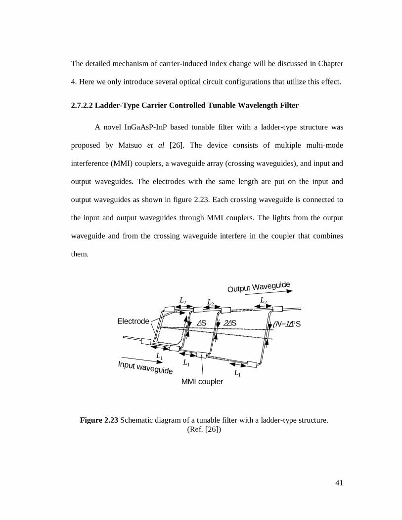
2.7.2.2 Ladder-Type Carrier Controlled Tunable Wavelength Filter
A novel InGaAsP-InP based tunable filter with a ladder-type structure was
proposed by Matsuo et al [26]. The device consists of multiple multi-mode
interference (MMI) couplers, a waveguide array (crossing waveguides), and input and
output waveguides. The electrodes with the same length are put on the input and
output waveguides as shown in figure 2.23. Each crossing waveguide is connected to
the input and output waveguides through MMI couplers. The lights from the output
waveguide and from the crossing waveguide interfere in the coupler that combines
them.
Figure 2.23 Schematic diagram of a tunable filter with a ladder-type structure. (Ref. [26])
MMI coupler
Input waveguide
Electrode
Output Waveguide
∆S 2∆S (Ν−1)∆S
L1L1
L1
L2L2L2

42
The crossing waveguides are designed such that the length difference between
two adjacent waveguides is ∆S. Let L1 = L2 and all the couplers have the same length.
Then all the couplers in the output waveguide have the same transmission peak
wavelength. The peak wavelength of the filter is
0effn S
mλ
∆= (2.25)
where neff is the effective refractive index of the waveguide and m is the diffraction
order. The diffraction order strongly affects the 3-dB bandwidth of the filter in the
way that the 3-dB bandwidth becomes narrower when it is increased.
When the refractive index in the input waveguide is reduced by carrier
injection, the optical path difference (OPD) between the output waveguide and the
crossing waveguides decreases. According to equation (2.25), this makes the peak
wavelength shorter. Similarly, reducing the refractive index in the output waveguide
increases the OPD, which makes the peak wavelength longer. The peak wavelength
change is given by
1or20
effn L
mλ
∆∆ = (2.26)
where ∆neff is the change of refractive index caused by carrier injection. So the actual
tunable wavelength range is 2(∆λ0)= 2(∆neff)L1or2/m. Equation (2.26) indicates that
increasing L1, L2 or ∆neff increases the wavelength shift while increasing of diffraction
order decreases the shift. As it was pointed out above that a large diffraction order
means a sharp peak in transfer function, there is a trade off between a narrow 3-dB

43
bandwidth and a wide tunable wavelength range. Also, there is a limitation in
increasing L1 and L2 when the size of a practical device is considered.
The InGaAsP-InP material tunable filter with a ladder-type structure proposed
by Matsuo has 15 crossing waveguides and a diffraction order of m = 20. The free
spectral range (FSR) is 74.4 nm and the total tunable range is 58 nm. The switching
time for two particular wavelengths that corresponding to injecting currents 0 and 20
mA is less than 10 ns.
The crucial points for the design of this kind of filter include the proper power
distribution of MMI (or waveguide-made) couplers and the optimum number of
crossing waveguides in the whole device. These are very important since the
interference conditions have to be satisfied.
2.7.2.3 Proposed Carrier Controlled Semiconductor AWG Tunable Filter
Widely tunable optical filters are needed in local area networks or tunable
light source applications [26]. As we have mentioned before, each semiconductor
material can have its refractive index changed with carrier injection. By using this
property of semiconductor material, we can also design carrier controlled AWG
filters.
A. Single-Wavelength Filter
Here we consider an AWG with one input and one output waveguide, as
shown in figure 2.24(a), where λ0, λ1, λ2, …, λn are the input wavelengths among
which λ0 is the central wavelength. To be convenient, both central waveguides in the

44
input side and output side of the previous design are chosen as the input port and
output port. Based on the previous analysis in section 2.5.3, it is quite obvious that the
output wavelength would be the central wavelength λ0 designed for this device. All
the other wavelengths are filtered out.
B. Same Length Electrode Controlled AWG Tunable Filter
The output wavelength for the filter in figure 2.24(a) is fixed (λ0). To realize
an adjustable wavelength filter, we can add electrodes to the arrayed waveguides in
the design as shown in figure 2.24(b). We first consider the case when all the
electrodes have the same length and let this length be z. As we know, the effective
refractive index of arrayed waveguides will be changed after electrical voltages are
Figure 2.24 (a) AWG Functioning As a Filter. (b) Electrode Controlled AWG Filter.
λi λ0,λ1,λ2,…,λn
Electrodes N
2
1
z
Input Output
λ0 λ0,λ1,λ2,…,λn
N
2
1
Output
Planar Star Coupler
Input
(a) (b)

45
applied to the electrodes. Let the change of the refractive index of waveguide j among
N arrayed waveguides be dncj, and also control the current injection in such a way that
∆dncj = dncj - dnc(j-1) = constant (2.27)
for all j, j = 1, 2, …, N, where ∆dncj is the difference between the changes of effective
refractive indices of two adjacent arrayed waveguides. We denote this constant as
∆dnc
∆dnc = ∆dncj (2.28)
Thus based on equation (2.19), we can get the new equation of AWG that satisfies the
phase match condition with current injection for this design
'λmzdnLn cc =⋅∆+∆⋅ (2.29)
where λ’ is the wavelength that passes the filter. Compare equation (2.29) with
equation (2.20), we can get
)/'1(/)'( 000 λλλλλ −⋅∆⋅−=−⋅∆⋅=⋅∆ LnLnzdn ccc (2.30)
where 0λ is the designed central wavelength. We see that the signal with wavelength
λ’ will pass the filter after electrical voltages are applied to the electrodes and
equation (2.30) is satisfied, while all the signals with other wavelengths will be
blocked.
C. Different Length Electrode Controlled AWG Tunable Filter
We can also design electrodes with different lengths zj. This is shown in figure
2.25, where the lengths of electrodes are designed as
z1 – z2 = z2 – z3 = … = zn-1 – zn = ∆z (2.31)
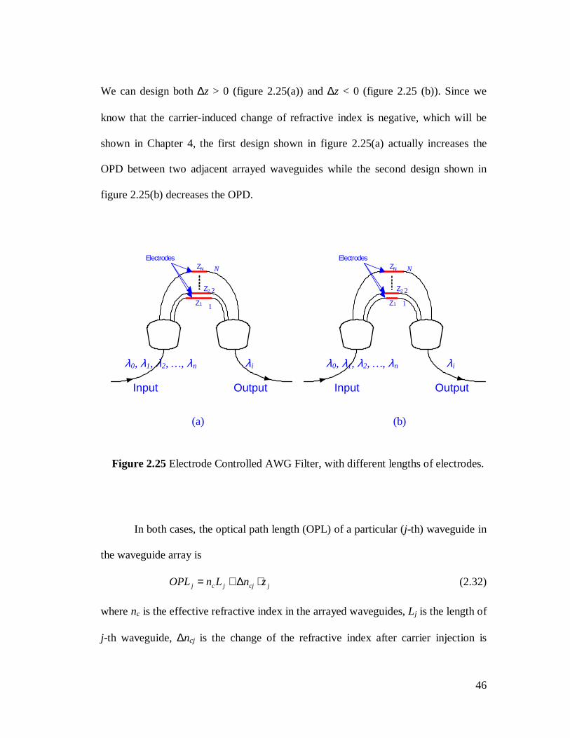
46
We can design both ∆z > 0 (figure 2.25(a)) and ∆z < 0 (figure 2.25 (b)). Since we
know that the carrier-induced change of refractive index is negative, which will be
shown in Chapter 4, the first design shown in figure 2.25(a) actually increases the
OPD between two adjacent arrayed waveguides while the second design shown in
figure 2.25(b) decreases the OPD.
In both cases, the optical path length (OPL) of a particular (j-th) waveguide in
the waveguide array is
jcjjcj znLnOPL ⋅∆+= (2.32)
where nc is the effective refractive index in the arrayed waveguides, Lj is the length of
j-th waveguide, ∆ncj is the change of the refractive index after carrier injection is
Figure 2.25 Electrode Controlled AWG Filter, with different lengths of electrodes.
λ0, λ1, λ2, …, λn
Input Output
λi
Electrodes
N
2
1
ZN
Z2
Z1
λ0, λ1, λ2, …, λn
Input Output
λi
Electrodes
N
2
1
ZN
Z2
Z1
(a) (b)

47
applied. For simplicity, we can let ∆ncj = ∆nc = constant. Under this condition, we can
get the new equation of AWG that satisfies the phase match condition with carrier
injection for this design as
'λmznLn cc =∆⋅∆−∆⋅ (2.33)
where ∆z is defined in equation (2.31). Compare equation (2.33) with (2.20), we have
λλ
λλ ∆⋅∆⋅=−⋅=∆⋅∆−0
0)'(Ln
mzn cc (2.34)
where ∆λ = λ’ - λ0. Thus
0λλ ⋅∆∆⋅∆−=∆L
z
n
n
c
c (2.35)
Equation (2.35) gives the wavelength range of the filter. As an example, for GaN
material that we will discuss in Chapter 5, we have nc = 2.312, ∆nc = -0.18 at λ0 =
1550 nm and carrier density N = 6 × 1019 cm-3. For our designed AWG, we have ∆L
equal to 64.79 µm. If we take ∆z = 75 µm, then ∆λ is about 140 nm.
From equation (2.35), we see that the larger is ∆z, the larger will ∆λ be.
Compare the two designs in figure 2.25, it is shown that figure 2.25(b) gives a better
design for wide range adjustable filter since it is easier to realize a large ∆z in this
design.
2.7.3 Design of Carrier Controlled AWG All-Optical Switch
Making devices with functionality of all optical switching is the final goal of
this research. Currently we only focus on the designs based on AWG structures.

48
2.7.3.1 Carrier Controlled Wavelength All-Optical Switch
A device consisting of two interleave-chirped AWG routers connected by
waveguides with phase shifters was proposed by Doerr [27]. Figure 2.26 shows an
example with two lines inputs and two lines outputs for this configuration. In the
example, the interleave chirp consists of adding an additional path length of λc/4 on
every other grating arm, where λc (=λc/n) is the wavelength of interest in the
waveguide. In general, an AWG router forms a radiation pattern on the output surface
Figure 2.26 Schematic diagram of the interleave cross connect. The inset in the lower left corner illustrates the Brillouin zones for star coupler 2. (Ref. [27])
'0Ω
'1−Ω
'0Ω
0Ω
1Ω
1−Ω
0Ω
Line 1Line 2
Star coupler
Phase shiffters
Waveguide gratingwith interleave chirp
Line 2Line 1
1
2
4
3
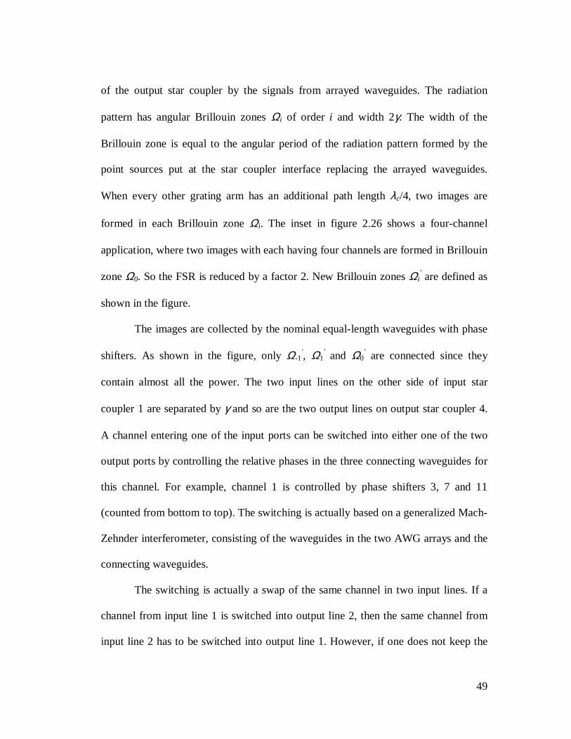
49
of the output star coupler by the signals from arrayed waveguides. The radiation
pattern has angular Brillouin zones Ωi of order i and width 2γ. The width of the
Brillouin zone is equal to the angular period of the radiation pattern formed by the
point sources put at the star coupler interface replacing the arrayed waveguides.
When every other grating arm has an additional path length λc/4, two images are
formed in each Brillouin zone Ωi. The inset in figure 2.26 shows a four-channel
application, where two images with each having four channels are formed in Brillouin
zone Ω0. So the FSR is reduced by a factor 2. New Brillouin zones Ωi' are defined as
shown in the figure.
The images are collected by the nominal equal-length waveguides with phase
shifters. As shown in the figure, only Ω-1', Ω1
' and Ω0' are connected since they
contain almost all the power. The two input lines on the other side of input star
coupler 1 are separated by γ and so are the two output lines on output star coupler 4.
A channel entering one of the input ports can be switched into either one of the two
output ports by controlling the relative phases in the three connecting waveguides for
this channel. For example, channel 1 is controlled by phase shifters 3, 7 and 11
(counted from bottom to top). The switching is actually based on a generalized Mach-
Zehnder interferometer, consisting of the waveguides in the two AWG arrays and the
connecting waveguides.
The switching is actually a swap of the same channel in two input lines. If a
channel from input line 1 is switched into output line 2, then the same channel from
input line 2 has to be switched into output line 1. However, if one does not keep the

50
same channels (wavelengths) in different input lines, one can realize the full scale
switching. For example, if we put channel 1 (λ1) and 2 (λ2) in input line 1 and
channel 3 (λ3) and 4 (λ4) in input line 2, we can switch any channel to either output
lines by controlling the relative phase shifters for that channel.
So far, this device has been demonstrated for 2 lines × 2 lines, 6 channel × 200
GHz spacing in InP [28]. We will focus on GaN/AlGaN material applications for 2
lines × 2 lines switching of the signals with same wavelength. Then, we will do
explorations in N × N (N>2) applications for the switching of the signals with
different wavelengths in each line. In a similar way, devices with N (N>2) input ports
and N output ports can be designed by employing an interleave chirp in each AWG
router to produce N images in each Ωi with enough waveguides to collect all of them.
If the channels or wavelengths in any input line are different than the channels in any
other lines, one can switch any channel in any line to any other lines by adjusting the
phase shifters properly. By doing this, an all-optical wavelength switch is realized.
A 1 × N Wavelength Switch can be realized with the same method as
mentioned above. A switch with 1 input and 8 outputs will be investigated. The input
part consists of only one input port instead of N input ports. The N channels with N
different wavelengths all are inputted through the common input port. By adjusting
the corresponding phase shifters, any wavelength channel can be switched to any one
of the N output ports. The details of this design will be discussed in Chapter 3.

51
2.7.3.2 Carrier Controlled Wavelength Add-Drop Switch
Based on the previous review, we propose a carrier controlled loop-back add-
drop switch as shown in figure 2.27. The device is based on the ideas of passive
Figure 2.27 Carrier Controlled Loop-Back Add-Drop Switch. (a) Schematic Diagram, (b) Corresponding Black Box.
(a)
N
2
1
ZN
Z2
Z1
ArrayedWaveguides
Loop Back
Loop Back
Main Input Main OutputWavelength-selective Output
Wavelength-selective Input
(b)
Main OutputMain Input
Wavelength-SelectiveOutput
Add selective-wavelength

52
wavelength-selective switches and add-drop multiplexers in section 2.7.1 and carrier
controlled semiconductor AWG filter in section 2.7.2. Figure 2.27(a) shows this
design. In the figure, all the outputs except for the main output and the one next to
main output are connected with their corresponding inputs. With the control of
electrodes applied to the arrayed waveguides, one can get the specific selected
wavelength signal at the wavelength-selective output, while all the other signals from
main input will be all transferred into the main output because of the symmetric
design of the AWG device.
2.8. Design of All-Optical Switch Networks
After investigating the single pieces of the devices in section 2.7.3, it is worth
doing further research in the designing of switch networks. For example, we can
design a 1 × N switch network as in figure 2.28, where the switch block is the one
shown in figure 2.27(b). One can compare the functionality of this design with the
one in section 2.7.3.1.
Figure 2.28 1 × N Wavelength Switch Network.
λ1, λ2, …, λN λ3, λ4, …, λN
λ1 λ2 λN-1
λN
λ2 λN-1

53
Since we would have 2 × 2 switch for same wavelength channels and N × N
switches for different wavelength channels, it would be reasonable to do further
investigations to realize any wavelength N × N switching.
2.9. Conclusion
In this chapter, we started from the introduction of telecommunications
network architecture. Then we gave a brief introduction of the second generation of
optical networks, discussed the network elements and their applications. To realize
the functionalities of those elements, especially the OXC, we reviewed the basic
components and their applications in an optical network. Then we briefly introduced
some large optical switch architectures and technologies. Based on that, we
particularly reviewed the principles of AWG and its applications. After that, we
proposed some possible architectures that can be realized with AWG principles.

54
3. Design of WDM Cross Connect Based on Interleaved AWG
(IAWG) and a Phase Shifter Array
3.1. Introduction
In the previous chapter, we have discussed that wavelength division
multiplexing (WDM) technique has been widely applied in the fiber-optic networks,
it effectively utilizes wide wavelength windows of the fiber and provides an
additional degree of freedom in optical networking [3]. In WDM systems, it is
critical to develop optical devices that can optically route wavelength channels from
any input port to any output port and thus to fully realize non-blocking N × N optical
switch functionality.
In chapter 2, we have briefly introduced arrayed waveguide gratings (AWG),
which have been used as WDM optical multiplexers (MUX) and demultiplexers
(DEMUX). In practical applications, refractive index tuning of arrayed waveguides
between the two star couplers in an AWG has been introduced to adjust and optimize
the transfer function of the device and it can also be used to perform WDM switching
with proper device structure design [6][7][29]. In silica-based AWGs, this index
tuning can be accomplished by locally heating each individual waveguide branch.
However this thermal coefficient-based tuning is usually too slow for an optical
packet switch. To overcome the speed limit of thermal tuning, AWG devices are also
made by semiconductor materials, such as GaAs and InP. In these devices, refractive
indices of branch waveguides can be changed by carrier injection. In general, the

55
speed of carrier-induced index change can be in the order of sub-nanosecond, which
is many orders of magnitude faster than thermal tuning and therefore it can
potentially be used to support an all-optical packet switch in the future.
In chapter 2, we have reviewed several different designs and device structures,
which have been proposed to realize AWG-based optical switches [6][7][27], where a
unique waveguide-interleaved-AWG (IAWG) structure was used. A 2 × 2 non-
blocking wavelength switch was demonstrated by using this approach and it can be
expanded to realize the switch size of N × N. However, this N × N switch illustrated
in [6] is not truly “any-to-any”, instead it is in a cyclical fashion [27], therefore, a
truly any-to-any non-blocking optical switch cannot be directly realized using the
structure proposed in [27]. In addition, a general design rule of interleaved AWGs is
not available so far, although it is necessary in the designing of different IAWGs.
Also, from a switch architecture point of view, a truly any-to-any N × N non-blocking
switch can be constructed by a group of 1 × N switches [30][1] using the Spanke
architecture as introduced in chapter 2. So it is also necessary to fully investigate the
design of 1 × N switch for a single wavelength using IAWG-based planar lightwave
circuit (PLC) and its applications to construct truly any-to-any N × N wavelength
switch.
In this chapter, we will utilize the Spanke architecture to realize a fully
functional non-blocking N × N WDM switch. From chapter 2, we have known that
the Spanke architecture is based on the combination of 2n (1 × N) optical switches.
We will show how to realize this 1 × N optical switch by using IAWGs. We will

56
present a detailed description of a self-consistent design rule of 1 × N all optical
switches. We will present the numerical results to illustrate the device characteristics
such as transfer functions and the extinction ratio of the switch. Then a detailed
design example of a 1 × 4 non-blocking WDM switch will be given and the phase
assignment at each phase shifter will be provided for various routing states. We will
also propose and investigate a simplified structure of a 1 × N WDM all-optical switch
based on a single IAWG with total a reflection at the end of each phase shifter.
Design considerations and device characteristics are discussed. It is also important to
note that the proposed 1 × N switch structure is a planar lightwave circuit (PLC) with
no waveguide crossing, therefore it can be monolithically integrated to create
sophisticated optical devices with more functionalities.
3.2. An Approach of an N ×××× N All Optical Switch
It is well known that any-to-any N × N non-blocking wavelength switches are
indispensable for optical networks. However, the design of a true any-to-any N × N
optical switch using PLC technology is not an easy task because of its complexity and
it has not been demonstrated so far. One modular approach to solve this problem is to
combine a group of 1 × N optical switches. This has been shown in the Spanke
architecture in chapter 2. To illustrate this architecture more clearly, figure 3.1 shows
a 4 × 4 non-blocking wavelength switch, which consists of eight 1 × 4 wavelength
switches with four of them at the input side and four of them at the output side. For
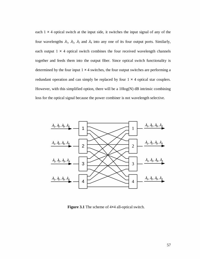
57
each 1 × 4 optical switch at the input side, it switches the input signal of any of the
four wavelengths λ1, λ2, λ3 and λ4 into any one of its four output ports. Similarly,
each output 1 × 4 optical switch combines the four received wavelength channels
together and feeds them into the output fiber. Since optical switch functionality is
determined by the four input 1 × 4 switches, the four output switches are performing a
redundant operation and can simply be replaced by four 1 × 4 optical star couplers.
However, with this simplified option, there will be a 10log(N) dB intrinsic combining
loss for the optical signal because the power combiner is not wavelength selective.
Figure 3.1 The scheme of 4×4 all-optical switch.
λ , λ , λ , λ 1 2 3 4
λ , λ , λ , λ 1 2 3 4
λ , λ , λ , λ 1 2 3 4
λ , λ , λ , λ 1 2 3 4
λ , λ , λ , λ 1 2 3 4
λ , λ , λ , λ 1 2 3 4
λ , λ , λ , λ 1 2 3 4
λ , λ , λ , λ 1 2 3 41
4
3
2
1
4
3
2

58
Since 1 × N wavelength switches are fundamental building blocks to realize
this any-to-any N × N non-blocking wavelength switch, the focus will be on the
development of a general design rule for a 1 × N wavelength switch in the following
sections.
3.3. The Scheme of the 1 ×××× N All-Optical Switch
The scheme of a 1 × N all-optical switch is presented in figure 3.2. This
optical switch consists of two IAWGs and is very similar to the one Doerr suggested
[27], as we have reviewed in subsection 2.7.3.1. Instead of having two or more input
ports at the input side as suggested by Doerr, figure 3.2 has only one input port while
still having N output ports. In this figure, star coupler 1 and 2 form the input N-
interleaved AWG (N-IAWG). Star coupler 3 and 4 form the output N-IAWG.
Between the two N-IAWGs are N subsets of phase shifters. Each subset has N phase
shifters. The input N-IAWG is designed in such a way that the input signal with
wavelength λi is directed into all l ij phase shifters, where l ij is the index of phase
shifters, i = 1, 2, …, N is the index of ports in each Brillouin zone (BZ) and j = 1,
2, …, N is the index of BZs as shown in figure 3.2. Moreover, the N-IAWG is
designed such that there is the same amount of signal power of wavelength λi
entering each l ij phase shifter. In this way, the routing of the input signal of
wavelength λi can be totally controlled by all l ij phase shifters so that 1 × N switching

59
functionality can be realized. The switching functionality will be further explained in
the next section.
3.4. Design of the N-IAWG
3.4.1. Functionality of N-IAWG
In section 3.3, we mentioned that N-IAWG is designed in such a way that the
input signal with wavelength λi is directed into all the output waveguides that connect
with l ij phase shifters. To be convenient, we also use l ij to denote these corresponding
output waveguides. Moreover, for optimum operation, the amount of signal power
entering each such waveguide should be the same.
Figure 3.2 Schematic diagram of 1 × N all-optical switch.
Star coupler
Phase shifters
Waveguide gratingwith interleave chirp
1
2
4
3
N
2
1N
2
1
N
2
1
λ , λ , λ ...1 2 N λ λ λ ...1 2 N
2
1
N
# of BZs
# of ports in each BZ

60
The above condition was mentioned for the N-IAWG that has only one input
port as in figure 3.2. It can be extended to a general N-IAWG that has N input ports as
shown in figure 3.3. When the separation between the input ports at star coupler 4 are
arranged properly, the N-IAWG can direct the signal of wavelength λi into the same
l ij output waveguides at star coupler 3, no matter which input port at star coupler 4 is
chosen. Moreover, the amount of the power entering into each of these output
waveguides at star coupler 3 is the same.
Based on the above description, we can see that for a signal at wavelength λi,
no matter which input port at star coupler 4 it enters, the output power always
distributes evenly among the same l ij output waveguides of star coupler 3, but the
phase distribution depends on the chosen input port. Because of reciprocity, if we
Figure 3.3 Schematic diagram of N-IAWG.
Star coupler
Waveguide gratingwith interleave chirp
N 2 N 21N 2 1
N 2 1
12
N
1
4 3
(
)

61
input a signal of wavelength λi into all those l ij waveguides at star coupler 3, each
with equal power, we can direct the signal into any one of the output ports at star
coupler 4 by adjusting the phase of each input properly. This explains the switching
functionality of figure 3.2. More details about this switching functionality will be
given later.
3.4.2. From AWG to IAWG
Similar to an AWG, an IAWG has an input star coupler and an output star
coupler. However, the path length difference between adjacent grating waveguides
for an IAWG deviates from that of an AWG to create a wavelength-dependent
focusing effect. To illustrate how to obtain the path length differences in IAWG, we
can start with the central phase matching equation of a conventional AWG as shown
in figure 2.13 [20][31]:
λθθ mdnLndn scis =+∆⋅+ )sin()sin( 0 (3.1)
Where m is the grating order, nc is the effective refractive index of the arrayed
waveguide, ns is the effective index of the slab in the output star coupler, ∆L is the
path length difference between two adjacent waveguides in the array, d is the
separation of adjacent waveguides at the star coupler, θi is the angle of i-th input port
to the direction of the central input port, θ0 is the diffraction angle in the output star
coupler and λ is the output wavelength. Compared with equation (2.20), we have
included the term related to the input side into equation (3.1) for general purpose.

62
From equation (3.1), the angular width ∆θ of the Brillouin zone (BZ), which
was defined in section 2.7.3., can be found as [32]:
dns
λθ =∆ (3.2)
The angular separation between -∆θ/2 and ∆θ/2 is commonly referred to as the
central Brillouzin zone. Only the output in the central BZ is generally of concern for
an AWG since most of the signal energy is concentrated in this area.
An N-IAWG varies the path length difference between the adjacent grating
waveguides so that each original BZ in an AWG is split into N equally spaced new
BZs [27]. Based on equation (3.2), we can find that the angular separation between
two adjacent BZs in an N-IAWG is,
Ndns
I
1⋅=∆ λθ (3.3)
The subscript I in equation (3.3) indicates interleave. Ideally the N BZs of an N-
IAWG split from the central BZ of an AWG should have the same amount of output
power according to the condition for optimum operation of N-IAWG as we
mentioned above. Each should have output power 1/N if the output power in the
central BZ of the AWG is normalized. Because most of the output power is
concentrated in this area [27], these N new BZs play important roles in the devices
consisting of N-IAWGs.

63
3.4.3. AWG Multiple-Beam Interference Condition
Although the general concept was discussed in the above section, the design
of an N-IAWG is not an easy task. Now we start presenting a general rule to design
an N-IAWG. To simplify the explanation, we illustrate the design rule through the
process of constructing a 4-IAWG as shown in figure 3.4, where figure 3.4(b) shows
that the central BZ of an AWG is split into four new BZs for the 4-IAWG. We start
with a conventional AWG, which has M waveguides in the arrayed grating. We then
divide these M waveguides into four subsets with the p-th subset composed of
waveguides p, p+4, p+8, p+12, ….., where p = 1, 2, 3, 4. In this arrangement,
removing any three of the four subsets, the remaining subset is still an AWG but with
path length difference 4∆L between adjacent waveguides and with waveguide
separation 4d at the input and output star couplers. With a single wavelength (λ0)
signal entering this remaining subset, the central phase match condition of this new
AWG can be obtained from equation (3.1)
00 ')sin()4()4()sin()4( λθθ mdnLndn scis =+∆⋅+ (3.4)
where m’ is the grading order of this new AWG. Therefore the angular separation
between two adjacent BZs at the output of the star coupler of this reduced AWG is,
)4(
' 0
dns
λθ =∆ (3.5)
Comparing equation (3.5) with equations (3.2) and (3.3), we can see that the BZ of a
subset AWG has the same angular width as a 4-IAWG, which is 1/4 that of the
original AWG. For each of the four subset AWGs, the radiation patterns are the same

64
in all the four new BZs denoted as Ω-1, Ω0, Ω1 and Ω2 as shown in Figure 3.4(b).
Since these 4 subsets combine only to form the original AWG, when all the 4 subsets
exist, there is only one maximum for the output field pattern in the entire angular
region of Ω-1, Ω0, Ω1 and Ω2, which is the central BZ of the original AWG. This
maximum output value happens in Ω0. This leads to the conclusion: when the input is
at wavelength λ0, the signals from the four subsets of the arrayed waveguides add
constructively in Ω0 and destructively in Ω-1, Ω1 and Ω2.
Figure 3.4 Diagram of output port distribution for an N-interleaved AWG. (a) An N-interleaved AWG, where N = 4; (b) Close-up of the output star coupler, where Ωi (i = -1, 0, 1, 2) denotes the new Brillouzin zones of this 4-IAWG. These new BZs were split from the central BZ of a conventional AWG before it was interleaved.
Zoom in
(b)
λ0
λ0 λ0 λ0
Ω2
Ω1
Ω0Ω -1
waveguide grating
d
(a)
λ0 λ0
1
23
4
Interleaved waveguide grating

65
3.4.4. Vector Illustration of the AWG Multiple-Beam Interference Condition
Table 3.1 Initial Vector Information for Constructing a 4-IAWG
BZ Vector Addition
Ω0
0
0,1A 0,2A 0,3A 0,4A
Ω1
01,1A
1,2A
1,3A
1,4A
Ω2
0
2,1A2,2A 2,3A2,4A
Ω-1
01,1 −A
1,2 −A
1,3 −A
1,4 −A

66
To systematically investigate the pattern of optical field distribution at the
output of the second star coupler of a conventional AWG, a vector representation can
be used. Let’s take subset p of the arrayed waveguides and denote its optical field
output in BZ Ωq as a vector qpA,
, where p = 1, 2, 3, 4 and q = -1, 0, 1, 2 in our above
example. We have
=⋅
==∑
=0 4
2 1, 1,- 0
0,1
4
1,
qA
q
Ap
qp
(3.6)
More specifically, the above vector additions are illustrated in table 3.1, where the
relative phase angles between the vectors are considered and the vectors qA ,1 are
treated as the references.
From table 3.1, we can see that although each subset of bridge waveguides by
itself would project the same amount of output power in each of these new BZs, Ωq,
the combination of the four subsets creates only one maximum which is located in BZ
Ω0 as the result of the vector addition of four field components in each BZ. If the
optical field magnitude created by each subset is qpAA ,0
= , the maximum output
optical power in Ω0 will be 2016A .
3.4.5. Additional Lengths to Arrayed Waveguides for Constructing 4-IAWG
In subsection 3.4.2, we mentioned that we could vary the path length
difference between the adjacent gratings to obtain an N-IAWG. For a conventional
AWG, this path length difference is [31]

67
cn
mL 0λ=∆ (3.7)
Table 3.2 Vector Information of a Constructed 4-IAWG
BZ Vector Addition
Ω0
0
0,1A0,2A 0,3A 0,4A
Ω1 01,1A
1,2A
1,3A1,4A
Ω2
0
2,1A 2,2A2,3A2,4A
Ω-1
01,1 −A
1,2 −A
1,3 −A1,4 −A

68
where m is the order of the array, λ0 is the center operating wavelength of the device
and nc is the effective index of the arrayed waveguide. Now we will show how to find
the additional waveguide lengths in addition to the ∆L in equation (3.7) to construct
an N-IAWG. We still use the 4-IAWG as an example. By rotating all the qA ,2 vectors
in table 3.1 by 180 degrees, the results of the vector additions turn out to be as in table
3.2. From table 3.2, it is shown that this π phase change makes the output power
equally split among the four BZs and the output power at each BZ be 204A , which is
1/4 of the maximum power shown in table 3.1.
To rotate all the vectors qA ,2 in table 3.1 by 180 degree means to change the
phase of the output vector from subset 2 waveguides by π. This can be realized by
adding additional length λ0c/2 to all the waveguides of subset 2, where λ0c = λ0/nc.
Furthermore, it can be easily seen that a 4-IAWG can be realized by adding an
additional length λ0c/2 to all the waveguides in any one of the four subsets while
keeping the waveguides in three other remaining subsets unchanged.
The procedure can be further simplified. In the above process, all four BZs
were considered in finding the additional waveguide lengths. Since the initial value of
the sum of all the vectors in each of the BZs Ω-1, Ω1 and Ω2 is zero, the magnitudes of
the vector summations in these three BZs will always be the same as long as each of
vectors qA ,2 turns a same amount of angle in each of these BZs. This fact tells us that
only one of these three BZs needs to be considered together with BZ Ω0 in the
designing of a 4-IAWG. This will be further explained later.

69
3.4.6. General Design Rule of N-IAWG
Based on the above example, a general rule in designing an N-IAWG can be
deduced. Firstly, one can divide the M arrayed waveguides in the AWG into N
subsets. In each subset, N⋅∆L is the path length difference between adjacent
waveguides and N⋅d is the arrayed waveguide separation at the input and output star
couplers. Secondly, one can find the initial vector information as in table 3.1. As
mentioned above, it is only needed to consider one more BZ, say Ω1, besides the
central BZ Ω0, where the maximum initial output power 20
2 AN exists. Then initially,
the sum of the vectors in BZ Ω0 and Ω1 are
0,1
1
0,0 ANAVN
p
p ⋅==∑=
Ω (3.8a)
01
1,1 ==∑=
Ω
N
p
pAV (3.8b)
So one can get the similar graphs as shown in table 3.1. Thirdly, one rotates any pair
of vectors 0,pA and 1,pA by the same angle δp, where p = 2, … N. We then rotate as
many pairs as necessary until the following condition is met
0,1
1
1,
1
0, 10 ANVAAVN
p
p
N
p
p ⋅==== Ω==
Ω ∑∑ (3.9)
At this point, one can record all the angular values, δp, and the additional length
needed for the waveguides in Subset p can be calculated as
cpL 0add 2
λπ
δ⋅=∆ (3.10)

70
where δp is in radians. Since 0 ≤ δp < 2π, ∆Ladd is always less than λ0c. Finding ∆Ladd
values is essential in the design of an N-IAWG.
3.4.7. Output Port Arrangement
From the above description, Ω0 is always used as the central BZ. This means
the output ports on the second star coupler have to be arranged in accordance with the
locations of BZs as illustrated in figure 3.4(a). Figure 3.4(b) is a detailed description
of the output star coupler, where if N is an odd number, the distribution of
waveguides is symmetrical about the center of the output star coupler, while if N is an
even number there is one extra output port on one side in comparison to the other side.
Table 3.3 Multiple sets of additional waveguide lengths [λc] in the design of an N-
IAWG
N Calculated Additional Arrayed Waveguide Lengths [λc]
2 1/4, 0
1/3, 0, 0 3
2/3, 0, 0
1/2, 0, 0, 0
1/4, 1/2, 1/4, 0
4
3/4, 1/2, 3/4, 0
0, 2/5, 1/5, 2/5, 0
0, 3/5, 4/5, 3/5, 0
0, 1/5, 3/5, 1/5, 0
5
0, 4/5, 2/5, 4/5, 0
6 1/12, 1/3, 3/4, 1/3, 1/12, 0

71
11/12, 0, 1/4, 2/3, 1/4, 0
3/4, 2/3, 3/4, 0, 5/12, 0
1/4, 1/3, 1/4, 0, 7/12, 0
1/12, 0, 3/4, 1/3, 3/4, 0
11/12, 2/3, 1/4, 2/3, 11/12, 0
0, 1/7, 3/7, 6/7, 3/7, 1/7, 0
0, 2/7, 6/7, 5/7, 6/7, 2/7, 0
0, 3/7, 2/7, 4/7, 2/7, 3/7, 0
0, 4/7, 5/7, 3/7, 5/7, 4/7, 0
0, 5/7, 1/7, 2/7, 1/7, 5/7, 0
7
0, 6/7, 4/7, 1/7, 4/7, 6/7, 0
0, 3/4, 1/2, 0, 1/2, 3/4, 0, 0
1/8, 1/4, 5/8, 0, 5/8, 1/4, 1/8, 0
0, 0, 1/4, 1/2, 0, 1/2, 1/4, 0
1/8, 0, 3/8, 1/2, 1/8, 1/2, 3/8, 0
0, 1/4, 0, 0, 1/2, 1/4, 1/2, 0
1/8, 1/4, 1/8, 0, 5/8, 1/4, 5/8, 0
8
7/8, 3/4, 3/8, 0, 3/8, 3/4, 7/8, 0
3.4.8. Comparison with Previous Results
The general rule discussed above can be used to calculate the additional
lengths ∆Ladd needed in arrayed waveguides of an AWG to transfer it into an N-
IAWG for any N value. Generally, multiple sets of additional lengths can be obtained
with the general design rule for a particular N. Table 3.3 shows the examples of the
additional lengths that were calculated by using this general rule for N = 2, 3, 4, 5, 6,

72
7, 8. All these values have been verified as good for constructing their respective N-
IAWGs.
Also shown in table 3.4 is another special set of additional lengths given by
Doerr in [27] where there is not a systematic design rule provided. Comparing
Doerr’s result with our simulation results presented in table 3.3, it can be found that
Doerr’s result is clearly only one of the solutions that can be obtained by using the
general design rule. For example, Doerr’s result of (3/4, 1/3, 3/4, 0, 1/12, 0) for N = 6,
is the same as our simulation result of (1/12, 0, 3/4, 1/3, 3/4, 0) for N = 6.
Table 3.4 Comparisons between the distributions of additional waveguide lengths [λc]
in the design of IAWG
N Additional Waveguide Lengths [λc] From [4]
2 1/4, 0
3 1/3, 0, 0
4 1/2, 0, 0, 0
5 1/5, 3/5, 1/5, 0, 0
6 3/4, 1/3, 3/4, 0, 1/12, 0
7 1/7, 3/7, 6/7, 3/7, 1/7, 0, 0
8 1/4, 1/2, 0, 1/2, 1/4, 0, 0, 0
This further confirms that the general rule gives us a way to find the additional
length distribution in arrayed waveguides needed for constructing an N-IAWG. The
fact that there are multiple sets of additional length distributions for each N value

73
benefits the design of an N-IAWG in that the optimum set of additional lengths can
be chosen.
3.4.9. Verification of Equal Vector Magnitudes in BZs of N-IAWG
In subsection 3.4.5, it was mentioned that the magnitudes of the vector
summations in BZs Ω-1, Ω1 and Ω2 are the same as long as each of vectors qA ,2 turns
a same amount of angle. This is obvious in the structure of 4-IAWG that was
discussed above. In this subsection, this consequence of equal vector magnitudes in
BZs will be verified for 5-IAWG in a relatively general way so that its method can be
applied to any N-IAWG for any values of N.
As in the case of 4-IAWG, to construct a 5-IAWG, we can divide the M
arrayed waveguides of a conventional AWG into five subsets with the p-th subset
composed of waveguides p, p+5, p+10, p+15, p+20, where p = 1, 2, 3, 4, 5. In this
arrangement, removing any four from the five subsets, the remaining subset is still an
AWG but with path length difference 5∆L between adjacent waveguides in the array
and with waveguide separation 5d at the input and output star couplers.
Similarly, let a single wavelength (λ0) signal enter this remaining subset, the
central phase match condition of this new AWG would be
00 ')sin()5()5()sin()5( λθθ mdnLndn scis =+∆⋅+ (3.11)
And the angular separation between two adjacent BZs at the output of the star coupler
of this reduced AWG is,

74
)5(
' 0
dns
λθ =∆ (3.12)
We can see that the BZ of a subset AWG has the same angular width as a 5-
IAWG, which is 1/5 that of the original AWG. Similar to the case of 4-IAWG, for
each of the five subset AWGs, the radiation patterns are the same in all the five new
BZs denoted as Ω-2, Ω-1, Ω0, Ω1 and Ω2 as in Figure 3.5b. Since these five subsets
combine only to form the original AWG, when all the five subsets exist, there is only
Figure 3.5 (a) Diagram of output port distribution for a 5-interleaved AWG. (b) Close-up of the output star coupler, where Ωi (i = -2, -1, 0, 1, 2) denotes the new BZs
of this 5-IAWG. These new BZs were split from the central BZ of a conventional AWG before it was interleaved.
Zoom in
(a)
λ0
1
23
4
Interleaved waveguide grating
λ0
λ0
waveguide grating
λ0
λ0 λ0 λ0
Ω0
Ω1
Ω-1Ω-2
Ω2
d
(b)

75
one maximum for the output field pattern in the combining angular region of Ω-2, Ω-1,
Ω0, Ω1 and Ω2, which is the central BZ of the original AWG. This maximum output
value happens in Ω0. This leads to the conclusion, the signals from the five subsets of
the arrayed waveguides add constructively in Ω0 and destructively in Ω-2, Ω-1, Ω1 and
Ω2.
Similarly, we can have a vector representation, which is shown in the
following equation
=⋅
==∑
=0 5
2 1, 1,- 2,- 0
0,1
5
1,
qA
q
Ap
qp
(3.13)
where p = 1, 2, 3, 4, 5 and q = -2, -1, 0, 1, 2 in this case. These vector additions are
illustrated in table 3.5, where the relative phase angles between the vectors are
considered and the vectors qA ,1 are treated as the references.
From table 3.5, if the optical field magnitude created by each subset is
qpAA ,0
= , the maximum output optical power in Ω0 will be 2025A . The optical
powers in other BZs are all equal to zeros just as in the case of 4-IAWG.
Our result in subsection 3.4.8 shows that if we keep the arrayed waveguide
lengths in the first and fifth subsets, add additional lengths of (2λ0c)/5 to all the
waveguides in the second and fourth subsets and add additional lengths of λ0c/5 to all
the waveguides in the third subset, the output optical powers in the five BZs will be

76
the same, which is equal to 205A , which is 1/5 of the maximum power shown in table
3.5. Thus a conventional AWG is turned into a 5-IAWG.
Table 3.5 Initial Vector Information of Constructing a 5-IAWG
BZ Vector Addition
Ω0
0
0,1A 0,2A 0,3A 0,4A 0,5A
Ω1 0
1,5A
1,1A
1,3A1,2A
1,4A
Ω2 0
2,5A
2,1A
2,3A
2,2A2,4A
Ω-1 0
1,5 −A
1,1 −A
1,3 −A1,2 −A
1,4 −A
Ω-2 0
2,5 −A
2,1 −A
2,3 −A
2,2 −A2,4 −A

77
As we know, adding additional lengths of λ0c/5 to the waveguides of the third
subset is equivalent to turning all the vectors qA ,3 by α radians, and adding additional
lengths of (2λ0c)/5 to the waveguides in the second and fourth subsets is equivalent to
turning all the vectors qA ,2 and qA ,4 by 2α radians, where α = 2π/5.
Figure 3.6 (a) The changes of the signal vectors in BZ Ω1 when an AWG changes to a 5-IAWG; (b) The changes of the signal vectors in BZ Ω2 when an
AWG changes to a 5-IAWG.
(a)
0
1,5A
1,1A
1,3A
1,2A
1,4A
0
1,5A
1,1A
1,3A1,2A
1,4A
,1,4A
2x
1x
5x4x
3x
,
1,3A
,1,2A
(b)
0
2,5A
2,1A
2,3A
2,2A
2,4A
0
,2,4A
2x
1x
5x4x
3x
,2,3A
,2,2A
2,4A2,2A
2,5A
2,3A
2,1A

78
Now let’s verify that the optical powers are the same in BZs Ω1 and Ω2 after
the vectors are turned the above angles. Figure 3.6 shows the changes of the signal
vectors in BZs of Ω1and Ω2. Figure 3.6a shows that vectors 1,2A , 1,3A and 1,4A are
changed to ,
1,2A , ,
1,3A and ,
1,4A . From equation (3.13) we know that
01,51,41,31,21,1 =++++ AAAAA (3.14)
So we have
)()( 15544343321,5
,
1,4
,
31
,
1,21,1 xxxxxxxxxxAAAAA ++++=++++ (3.15)
Where
)( 43321,2
,
1,2 xxxxAA +=− (3.16a)
431,3
,
1,3 xxAA =− (3.16b)
)( 15541,4
,
1,4 xxxxAA +=− (3.16c)
Let
032 Vxx = , (3.17)
We have
ααα 3015
2054043 , , jjj eVxxeVxxeVxx === , (3.18)
Combine equations (3.18) and (3.15),
)21(
)()(32
0
30
200001,5
,
1,4
,
31
,
1,21,1
ααα
αααα
jjj
jjjj
eeeV
eVeVeVeVVAAAAA
+++=
++++=++++ (3.19)
Similarly, from figure 3.6b, we can get

79
)21(
)()(
)()(
320
003
02
00
43321554432,5
,
2,4
,
2,3
,
2,22,1
ααα
αααα
jjj
jjjj
eeeV
eVVeVeVeV
xxxxxxxxxxAAAAA
+++=
++++=
++++=++++
(3.20)
So from (3.19) and (3.20), we can see that
2,5
,
2,4
,
2,3
,
2,22,11,5
,
1,4
,
31
,
1,21,1 AAAAAAAAAA ++++=++++ (3.21)
This verifies that the optical powers are the same in BZs Ω1 and Ω2 after the vectors
are turned their relative angles. If we look at figure 3.6 clearly, we can see that the
result in equation (3.21) can be obtained directly from the figure.
Furthermore, by using the same vector method, we can get
5 ,4 ,3 ,2 ,1for 5)( 0,1
5
1
,
,
, =⋅=−∑=
qAAAp
qpqp
(3.22)
This verifies that optical powers are all the same in BZs of the 5-IAWG. By using this
same method, we can verify that the optical powers are split evenly among the BZs of
an N-IAWG. This guarantees that the functionality of an N-IAWG is feasible.
3.4.10. Verification of N-IAWG with Numerical Simulation
In the above sub-sections, the general design rule has been given out, and
multiple sets of additional lengths are calculated and compared with a special set of
additional lengths presented by Doerr. In this subsection, numerical simulations will
be applied to verify that the additional lengths applied to the arrayed waveguides do
change an AWG to an IAWG. Again the 4-IAWG as shown in figure 3.4 is taken as
an example. In the simulation, the 4-IAWG is designed for four channels with
channel wavelengths 1549.2 nm, 1549.6 nm, 1550.0 nm and 1550.4 nm. The

80
wavelength λ0 used to design the 4-IAWG was 1550.0 nm, and a signal with constant
spectrum between 1549.2-1550.8 nm as the input. Since the amplitude distribution of
a star coupler is a Gaussian distribution [33], the intensity distribution at the output
side of the first star coupler in 4-IAWG, which is position 2 in figure 3.4, is also a
Gaussian, which can be expressed as
),,()( 0 mMImI σ= (3.23a)
where I0 is a discrete Gaussian distribution, which is expressed as
−−= 2
2
0 22
exp2
1),,(
σπσσ
Mm
mMI (3.23b)
In the application, m = 1, 2, ⋯, M, is the index of the waveguides in the array. M is
the total number of the waveguides in the array. σ is the standard variance of the
distribution. In the design example of 4-IAWG, the following values are chosen: M =
64, σ = σ0 = 0.36*(W/2), where W = 63D0 is the width of the output range of the star
coupler with D0 as the output waveguide separation.
Matlab programs had been composed, and simulations had been run. The
simulation results are shown in figure 3.7. Figure 3.7a shows the output powers of the
four output ports for wavelength λ0 = 1550 nm. It is quite clear that these four outputs
have exactly the same powers at the same wavelengths with peak value at λ0 = 1550
nm. Figure 3.7b, 3.7c and 3.7d show the output powers of three other channels from
12 other output ports as shown in figure 3.4a. Each channel relates to four output
81
ports. It can be seen that all these simulation results have verified the design of 4-
IAWG.
Figure 3.7 Verification of 4-IAWG. The output powers at its related four output ports are exactly the same for each channel. (a) Central channel with wavelength λ0 = 1550 nm, (b) Channel of wavelength 1549.2 nm, (c) Channel of wavelength
1549.6 nm, (d) Channel of wavelength 1550.4 nm.
(a)
1549.2 1549.4 1549.6 1549.8 1550 1550.2 1550.4 1550.6 1550.8-70
-60
-50
-40
-30
-20
-10
0
wavelength(nm)
dB

82
Figure 3.7 (b) and (c)
(b)
1549.2 1549.4 1549.6 1549.8 1550 1550.2 1550.4 1550.6 1550.8-70
-60
-50
-40
-30
-20
-10
0
wavelength(nm)
dB
(c)
1549.2 1549.4 1549.6 1549.8 1550 1550.2 1550.4 1550.6 1550.8-70
-60
-50
-40
-30
-20
-10
0
wavelength(nm)
dB

83
3.4.11. Transfer function of an N-IAWG
Since the design of an N-IAWG has been verified, it is time to find its transfer
function. With the intensity Gaussian distribution at the star coupler as shown in
equation (3.23), the output amplitude at one of the output ports of an N-IAWG can be
expressed as,
[ ](
[ ] )s
c
M
m
NlxmQmxP
NmADDLLmLjkmBmAlClA
⋅−+−+
⋅−+∆⋅−+⋅⋅= ∑=
))(),1(())1(),0((
)1()1(exp)()()(),(
21
01
IAWG λ (3.24)
Figure 3.7 (d)
(d)
1549.2 1549.4 1549.6 1549.8 1550 1550.2 1550.4 1550.6 1550.8-70
-60
-50
-40
-30
-20
-10
0
wavelength(nm)
dB

84
where l is the position index of the output ports at the second star coupler, λ is the
channel wavelength, L0 is the length of the shortest waveguide in the waveguide array,
Nc is the refractive index of waveguide while Ns is the refractive index of the slab
region of the star coupler. ∆L is the path length difference between adjacent arrayed
waveguides of a traditional AWG. ADDL gives the additional lengths added to the
arrayed waveguides in AWG to obtain IAWG. A(m) is the amplitude distribution at
the input side of the arrayed waveguides, B(m) is the modification factor for the
output of the arrayed waveguides transmitting to the output ports at the second star
coupler. C(l) is the modification factor to the output at the l-th output port of the
second star coupler due to Gaussian distribution. P(x1, m) is the path length from the
input port at x1 through the first star coupler to the m-th arrayed waveguide. Q(m, l) is
the path length from the m-th arrayed waveguide through the second star coupler to
the l–th output port. Here m is 0 for the shortest waveguide in the array. According to
[33], we have
0
101 2
)12(),(
R
dxmRmxP
−−= (3.25)
0
202 2
)12(),(
R
dxmRxmQ
−−= (3.26)
where, x1 and x2 denotes the positions of the input port and output port on the relative
star couplers, d is the arrayed waveguide separation, R0 is the radius of curvature of
the star coupler. The distribution factors in equation (3.24) are expressed as
[ ] 2/100 ),,()()( mMImBmA σ== (3.27)

85
[ ] 2/1
000 ),,2/()2()( lMIlC σπσ ⋅= (3.28)
where equation (3.27) is due to the principle of reciprocity. The distribution C(l) is
normalized and the half width as in equation (3.28) is due to the Rowland structure of
the star coupler. Equation (3.24) can be written as
[ ](
[ ] )s
c
M
m
NlxmQmxP
NmADDLLmLjkmIlClA
⋅−+−+
⋅−+∆⋅−+⋅⋅= ∑=
))(),1(())1(),0((
)1()1(exp)()(),(
21
01
IAWG λ (3.29)
Define a function of an IAWG as
[ ](
[ ] )s
c
M
m
NlxmQmlxP
NmADDLLmLjkmIlClCllB
⋅−+−+
⋅−+∆⋅−+⋅⋅⋅= ∑=
))(),1(())1(),((
)1()1(exp)()()(),,(
2211
01
2121IAWG λ
(3.30)
Then
),,0(),( IAWGIAWG λλ lBlA = (3.31)
3.4.12. Extinction Ratio Versus the Interleaved Number N
In our definition, extinction ratio is the difference between the maximum
value (dB) of the central peak and the maximum value (dB) of the side lobes as
shown in figure 3.7. Extinction ratio versus the interleaved number N for a single
wavelength channel was calculated. The result is shown in table 3.6. From table 3.6,
we see that the extinction ratio does not change very much with the changes of the
number of the interleaves. This can be explained by the multi-beam interferences at

86
the output star coupler. It is obvious that the total number of waveguides at the input
side of the output star coupler remains the same although the interleaves are different.
It is still the same number of waveguides that join the interferences at each output
port of the output star coupler. The extinction ratio thus remains the same. This is a
very important result. It means we can design as many numbers of interleaved AWG
as possible.
Table 3.6 Extinction ratio (ER) versus the interleaved number N
N 1 2 4 5 6 7 8
ER (dB) 64.0 61.5 57.0 60.5 58.9 55.9 62.0
3.5. Realization of a 1 ×××× N All Optical Switch
3.5.1. The Transfer Function of a 1 ×××× N All-Optical Switch
Since a 1 × N All-Optical Switch consists of two N-IAWGs and the transfer
function of a single N-IAWG is shown in equation (3.29), we can similarly get the
transfer function of the 1 × N All-Optical Switch. With the result in equation (3.29),
the output signal amplitude at one of output ports of star coupler 2 in figure 3.2 can be
expressed as
),(),( IAWGout2 λλ lAlA = (3.32)

87
After the signal output from the l-th output port of the first N-IAWG going through its
connected phase shifter, the complex amplitude of the signal becomes
)],(exp[),(),( out2out3 λθλλ ljlAlA ∆⋅= (3.33)
This is the signal amplitude at the entrance of star coupler 3 as designated in figure
3.2. ∆θ(l, λ) is the phase change caused by the l-th phase shifter to the signal of
wavelength λ. This will be discussed further later.
The output signal from the l-th phase shifter contributes an output at the n-th
output port of star coupler 4, which can be expressed as
),,(),(),,( IAWGout3out λλλ nlBlAnlB ⋅= (3.34)
Adding contributions of the signals from all the phase shifters, the total output at the
n-th output port of star coupler 4 for the signal of wavelength λ can be expressed as
∑⋅
==
NN
l
nlBnA1
out4out ),,(),( λλ (3.35)
Equations (3.32)-(3.35) give out the transfer function of a 1 × N All-Optical Switch.
3.5.2. Switching Functionality Verification and Phase Change Information
The functionality of an N-IAWG has been explained in subsection 3.4.1. To
realize the 1 × N switching functionality with the structure of figure 3.2, all we need
to do is to verify that it is possible to switch a signal with one specific wavelength λi,
i = 1, 2, …, N, to any one of the output ports from the single input port. This is
because signals with different wavelengths are controlled by different sets of phase
shifters. Switching a signal of specific wavelength with a specific set of phase shifters

88
will not affect the signals of other wavelengths. According to the description in
section 3.4, the realization of the switching functionality is due to the symmetry of the
structure of figure 3.2. For a single wavelength channel, all we need to do is to collect
the phase information at its N related output ports of star coupler 2 and the phase
information we needed at the N related input ports of star coupler 3 to direct the
signal to a specific output port at star coupler 4.
Now if we let the wavelength channel λi input into the n-th output port at star
coupler 4 in figure 3.2, we should be able to collect its output signal at the N related
input ports of star coupler 3. We denote the phase at the k-th input port of star coupler
3 as θn(k,λi), where k is equal to i, N+i, 2N+i, …, or (N-1)N+i. Then we know if the
same single wavelength channel is input from the only central input port of star
coupler 1, the signal will be switched to the n-th output port at star coupler 4 as long
as the phase at the k-th input port of star coupler 3 is θn*(k,λi), the conjugate of
θn(k,λi), for all k = i, N+i, 2N+i, …, (N-1)N+i. We can write these in the following
equations
)],(exp[),(),( 0out2out2 iii kjkAkA λθλλ ⋅= (3.36)
)],(exp[),(),( *out2out3 inii kjkAkA λθλλ ⋅= (3.37)
As long as equation (3.37) is satisfied, the signal will be switched to the n-th output
port at star coupler 4. From equation (3.36) and (3.37), we can get the phase change
needed in the k-th phase shifter as
),(),(),( 0*
iini kkk λθλθλθ −=∆ (3.38)

89
where λi is the wavelength of the single channel and n denotes the destination output
port of the signal. θ0(k,λi) in equations (3.36) and (3.38) is the phase information of
channel λi at the k-th output port of star coupler 2. The arrangement of the output
ports can be seen in figure 3.8 for the example of a 1×4 switch, where only the four
phase shifters related to wavelength λ0 are shown.
It can be seen that every single phase shifter needs an independent control
signal to adjust the phase needed. Since there are N2 phase shifters as shown in figure
3.2, there are N2 degrees of freedom in our 1×N structure.
Figure 3.8 Schematic diagram of 1×4 switch for single channel with wavelength λ0.
1
2
4
3
λ 0
1
2
1
X
1 2 43
λ 0
-D
D 2D
0-D
D 2D
0
2D0-D
D
X
X
90
3.5.3. Simulation Verification ------An Example
Although the above description of the structure is very reasonable, it is still
important to do simulation verifications to obtain the practical requirements on the
parameters. This will help us to know if the suggested structure works in real
applications. We did a simulation for a 1×4 switch. The switching functionality was
verified. This specific schematic diagram of a 1×4 switch is shown in figure 3.8. In
this scheme, the input port at start coupler 1 is located at the center of the star coupler.
The output ports at star coupler 2 are located at the positions of –D, 0, D and 2D as
shown in the figure. The locations of the input ports and the output ports at star
couplers 3 and 4 are also shown in the figure, where X is the coordinate, D is the
waveguide separation. To simplify the diagram, we have only drawn four phase
shifters here. These phase shifters are connected to the four output ports on the star
coupler 2. These four output ports are the only ones to which the signal of wavelength
λ0 is directed in the four new central BZs of the 4-IAWG. In our real simulation,
however, all 4×4 = 16 phase shifters were involved so that the crosstalk caused by
this design could be evaluated.
Figure 3.9 shows one of our simulation results. The four channel wavelengths
are 1549.2 nm, 1549.6 nm, 1550.0 nm and 1550.4 nm with a channel spacing of 0.4
nm. Figure 3.9 shows that 1550.0 nm channel was switched to output port 1 (-D),
1549.6 nm channel to output 2 (0), 1550.4 nm channel to output 3 (D) and 1549.2 nm
channel to output 4 (2D). For comparison, we put these graphs together in figure 3.10.

91
We can see from figure 3.10 that the crosstalk is about –32 dB or less, which verifies
that the scheme is applicable.
Figure 3.9 Simulation result of 1×4 switch for four wavelength channels with wavelengths 1549.2 nm, 1549.6 nm, 1550.0 nm and 1550.4 nm with a channel
spacing of 0.4 nm. The 1550.0nm channel was switched to output port 1, 1549.6nm channel to output 2, 1550.4nm channel to output 3 and 1549.2nm
channel to output 4.
1549 1549.5 1550 1550.5-60
-40
-20
0
Wavelength (nm)
Tra
nsm
issi
on
(dB
)
1549 1549.5 1550 1550.5-60
-40
-20
0
Wavelength (nm)T
ran
smis
sio
n(d
B)
1549 1549.5 1550 1550.5-60
-40
-20
0
Wavelength (nm)
Tra
nsm
issi
on
(dB
)
1549 1549.5 1550 1550.5-60
-40
-20
0
Wavelength (nm)
Tra
nsm
issi
on
(dB
)

92
The values of phase changes and related refractive index changes required in
the phase shifters in our simulation are presented in tables 5 and 6. Here we have
assumed that the equal length waveguides are connected to the phase shifters. The
relationship between phase changes and the refractive index changes is
θπ
λ ∆⋅=∆)(2 LP
n (3.39)
Figure 3.10 Simulation result of 1×4 switch for four wavelength channels with wavelengths 1549.2 nm, 1549.6 nm, 1550.0 nm and 1550.4 nm with a channel
spacing of 0.4 nm. The crosstalk between channels is round –32 dB or less.
1549 1549.2 1549.4 1549.6 1549.8 1550 1550.2 1550.4 1550.6-60
-50
-40
-30
-20
-10
0
Wavelength (nm)
Tra
nsm
issi
on(d
B)

93
where LP is the length of the phase shifters. From table 3.8, we can see that the
maximum refractive index change needed in a phase shifter with a length of 2 mm is
6.918 × 10⁻⁴ to switch the signal of wavelength 1550 nm. From our previous research
[29][34], we know that the maximum possible refractive index change at wavelength
1550 nm is ~9 × 10⁻⁴. This result clearly verifies that the switching is realizable.
Table 3.7 Phase changes (∆θ) needed in phase shifters for each output port selection
in 1×4 all-optical switch (λ = 1550 nm)
Output
Choice
Phase shifter 1
(radians)
Phase shifter 2
(radians)
Phase shifter 3
(radians)
Phase shifter 4
(radians)
Port 1 1.659 -3.128 1.510 3.007
Port 2 0.8362 -0.8091 -2.454 2.184
Port 3 -3.128 1.510 3.007 1.362
Port 4 -0.8091 0.6874 2.184 -2.602
Table 3.8 Refractive index changes (∆n) needed in phase shifters with length LP = 2
mm for each output port selection in 1×4 all-optical switch (λ = 1550 nm)
Output
Choice
Phase shifter 1 Phase shifter 2 Phase shifter 3 Phase shifter 4
Port 1 2.046e-004 -3.858e-004 1.863e-004 3.709e-004
Port 2 1.031e-004 -0.998e-004 -3.027e-004 2.694e-004
Port 3 -3.858e-004 1.863e-004 3.709e-004 1.680e-004
Port 4 -0.998e-004 0.848e-004 2.694e-004 -3.209e-004

94
3.5.4. The Scheme of Mirror 1 ×××× N All-Optical Switch
The simulation verifies that the scheme shown in figure 3.2 works. It is based
on the symmetry of the structure with two N-IAWGs. In a real application, there are
always some mismatches between the two N-IAWGs caused in fabrication process.
The mismatches can cause extra signal loss. To avoid this shortage, we made
modifications on the scheme in figure 3.2 to simplify the structure. The new designed
structure is shown in figure 3.11. Instead of using two N-IAWGs, we use just one in
this new design by using a mirror as shown in the figure. The waveguides at the input
side of star coupler 1 are all used for the output ports except for the central one. This
central input waveguide is used as the only input port for this new design. Obviously
there are only N-1 output ports. So this new design essentially is a 1 × (N-1) all-
Figure 3.11 Mirror scheme of 1 × N all-optical switch.
1
2
N
2
1N
2
1
N
2
1
λ , λ , λ ...1 2 N
2
1
NMirror
......
21λ , λ ’ ’
λ N’

95
optical switch. The simplicity of the structure is the tradeoff of one less output
channel. But the advantage of this scheme is quite clear. By using the same N-IAWG
for input and output in the scheme shown in figure 3.11, the possible mismatch
between the input and output IAWGs in the previous scheme is successfully avoided.
We can always have the peak value at the output ports as long as the phase change
requirements in the phase shifters are satisfied. Figure 3.12 shows a simulation result
for the mirror structure for N = 4. As we mentioned above, three channels can be
applied to the structure.
Figure 3.12 Simulation result of the mirror scheme of 1 × (N–1) all-optical switch for N = 4.
1549.4 1549.6 1549.8 1550 1550.2 1550.4 1550.6-50
-45
-40
-35
-30
-25
-20
-15
-10
-5
0
Wavelength (nm)
Tra
nsm
issi
on(d
B)

96
3.6. Conclusion
In this chapter, we first proposed a uniquely fully functional non-blocking N ×
N WDM all-optical switch. Then we presented a complete theory or method for
designing a 1 × N all optical switch, which is the key element in the designing of an N
× N WDM all-optical switch. Since the 1 × N all optical switch is an application of N-
AWG, the general rule for the design of an N-IAWG was thus developed and
presented. It was found that multiple solutions could be obtained by using the general
rule. The comparison between the results obtained by using the general rule and the
results from other papers showed that the general rule is practical and the results
previously published are special cases under this general rule. It allows us to find the
optimum additional lengths added to the arrayed waveguides of an AWG to construct
an N-IAWG. By applying the general rule, any number of interleaved IAWGs can be
developed. The 1 × N freely switching functionality for a single wavelength channel
was then discussed. Various simulation results were presented and the feasibility of
this proposed switch configuration was discussed. It is also important to note that the
1 × N switch building block is a planar device with no waveguide crossings so that it
can be monolithically integrated into more complicated devices. Finally a unique
reflective 1 × (N–1) scheme based on an N-IAWG was presented, which significantly
simplifies the device configuration. A numerical simulation carried out for this
structure verified its feasibility and the advantages of this structure were also
discussed. The theoretical foundation established in this chapter for the design of an
any-to-any N×N optical wavelength switch is generally applicable to many material

97
systems and will be useful in the design of future large-scale optical integrated
circuits.

98
4. Carrier Induced Refractive Index Changes in GaN/AlGaN
Semiconductors
4.1 Introduction
In chapter 2, we briefly introduced the design of waveguide devices with
carrier-controlled refractive indices, especially the design of carrier-controlled AWG
all-optical switch. In chapter 3, we presented the scheme of 1 × N all-optical switch,
which requires carrier-controlled phase shifters, which can be made from III-V
semiconductors. Group III-V semiconductors are playing an increasingly important
role in integrated optics, because they offer the potential for integration of sources,
detectors, switches, and modulators onto the same chip [35]. Guided-wave switching
and modulation can be achieved by electro-optical effect where the refractive index of
the material can be controlled by the electric field across it. Also, free-carrier-induced
optical switching in InGaAsP-InP has been demonstrated [36], where the optical
switch was realized by using complete internal reflection, due to the free-carrier-
induced refractive index decrease at some designed area. In [36], the carrier-induced
refractive index of the same material system was also roughly measured, at the order
of 10-3, with the change of the current density. In [37], optical generation of free
carriers was applied to control the transmission in InGaAsP epilayers upon InP
substrates. Efficient GaAs-AlGaAs depletion-mode phase modulators were fabricated
in which both electric field and carrier effects were significant [38][39]. Carrier-
induced refractive index changes are also important for laser design [40][41]. The

99
refractive index change produced by injection of free carriers in InP, GaAs, and
InGaAsP have been theoretically estimated in [35], in which three basic phenomena
of III-V semiconductor materials were discussed: bandfilling, band-gap shrinkage,
and free-carrier absorption (plasma effect).
In this dissertation, since our attention is focused on the application of III-
nitride-based photonic devices, we will first review the theory of these three
important carrier effects in this chapter, and then we will utilize them to estimate the
carrier-induced refractive index changes in GaN and AlGaN. As we have mentioned
earlier, AlGaN semiconductors are highly transparent in the infrared area, and their
refractive indices can be modified by the control of Al concentration. These materials
are good candidates for planar lightwave circuits. They can be made into a fast
switchable optical PHASAR to realize all-optical switches because their refractive
indices are also dynamically adjustable through carrier-injection [29]. Previous
studies of carrier-induced refractive index change in GaN semiconductors were
mainly focused on the UV and visible wavelength regions near the bandgap; it is
important to extend these studies into the infrared wavelength region for optical
communications. The efficiency of carrier-induced index change is a critical
parameter for switchable PHASAR applications.
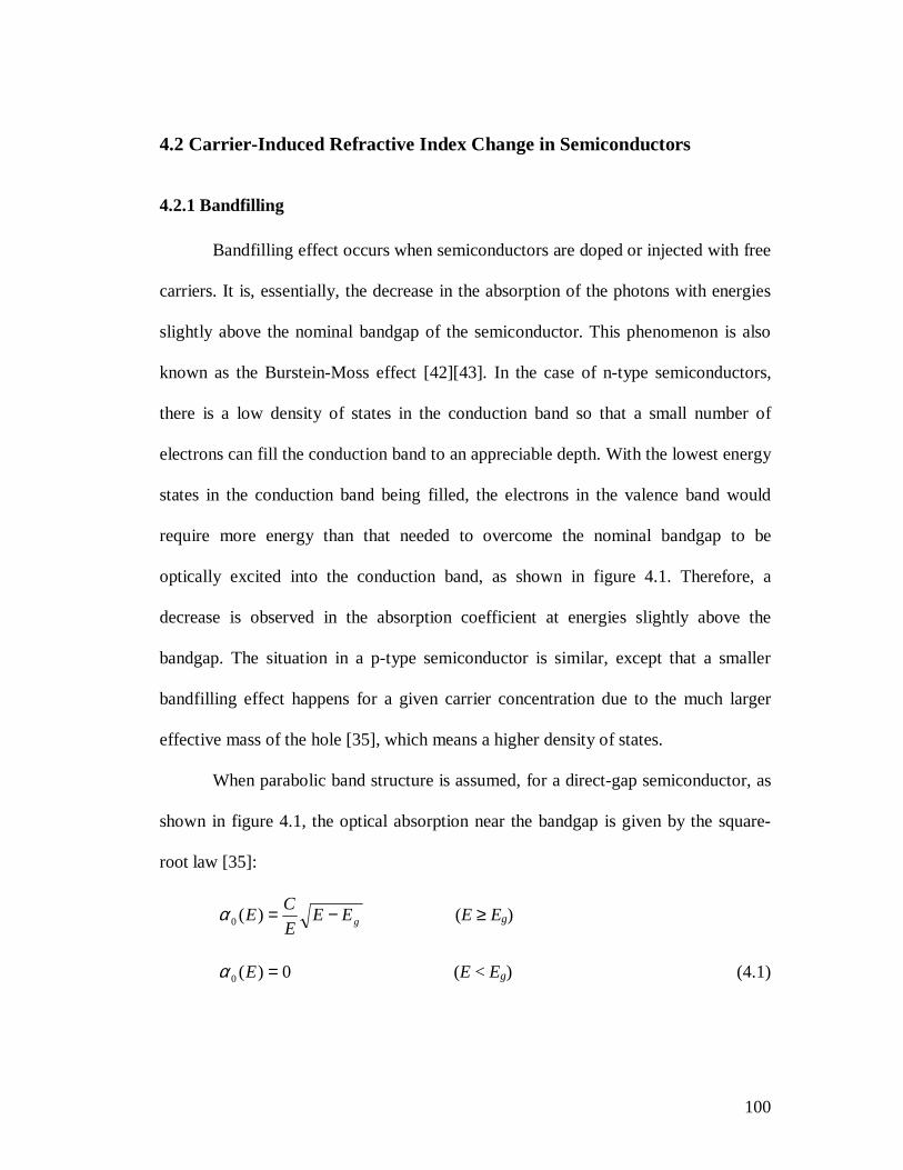
100
4.2 Carrier-Induced Refractive Index Change in Semiconductors
4.2.1 Bandfilling
Bandfilling effect occurs when semiconductors are doped or injected with free
carriers. It is, essentially, the decrease in the absorption of the photons with energies
slightly above the nominal bandgap of the semiconductor. This phenomenon is also
known as the Burstein-Moss effect [42][43]. In the case of n-type semiconductors,
there is a low density of states in the conduction band so that a small number of
electrons can fill the conduction band to an appreciable depth. With the lowest energy
states in the conduction band being filled, the electrons in the valence band would
require more energy than that needed to overcome the nominal bandgap to be
optically excited into the conduction band, as shown in figure 4.1. Therefore, a
decrease is observed in the absorption coefficient at energies slightly above the
bandgap. The situation in a p-type semiconductor is similar, except that a smaller
bandfilling effect happens for a given carrier concentration due to the much larger
effective mass of the hole [35], which means a higher density of states.
When parabolic band structure is assumed, for a direct-gap semiconductor, as
shown in figure 4.1, the optical absorption near the bandgap is given by the square-
root law [35]:
gEEE
CE −=)(0α (E ≥ Eg)
0)(0 =Eα (E < Eg) (4.1)

101
where E = ħω is the photon energy, Eg is the band-gap energy, and C is a constant
involving materials parameters, matrix elements between periodic parts of the Bloch
states at the band edges, and fundamental constants [43]. At direct gap for III-V
semiconductors, the valence bands are degenerated, due to the existence of both light-
and heavy-hole bands contributing to the absorption process, as shown in figure 4.1.
In this case, the equation of optical absorption near the bandgap, equation (4.1), is
modified as:
Figure 4.1 Energy band structure and bandfilling effect for direct-gap semiconductor. Absorption of a photon can occur only between occupied valence band states and unoccupied conduction band states. (Ref. [35])
Eah
Eal
Conduction Band
Eg
Ebl
EFV
EFC
Heavy Holes
Light HolesValence Bands
Ebh
ωℏωℏ

102
0( ) hh lhg g
C CE E E E E
E Eα = − + − (E ≥ Eg)
0)(0 =Eα (E < Eg) (4.2)
where Chh and Clh refer to heavy and light holes, respectively. The values of C for
different materials can be estimated by fitting equation (4.1) to experimental
absorption data [44].
The constants Chh and Clh in the above equation can be calculated from the
following equations [35]:
3/ 2
3/2 3/ 2ehh
hhehh elh
C Cµ
µ µ
= + (4.3a)
3/2
3/2 3/2elh
lhehh elh
C Cµ
µ µ
= + (4.3b)
where µehh and µelh are the reduced effective masses of the electron-hole pairs [43],
which can be obtained from
11 1
ehhe hhm m
µ−
= +
(4.4a)
11 1
elhe lhm m
µ−
= +
(4.4b)
where me, mhh and mlh are the effective masses of electrons, heavy holes, and light
holes, respectively.
The values of C, Chh and Clh are given in table 4.1 [35]. It can be seen that
about two-thirds of the absorption results from heavy holes and one-third from light
holes in all three materials.

103
Table 4.1: Values of Semiconductor Parameters (T = 300 K) [35]:
InP GaAs In0.82Ga0.18As0.40P0.60
Eg(eV) 1.34 1.42 1.08
C(cm-1⋅s-1/2) 4.4 × 10¹² 2.3 × 10¹² 3.2 × 10¹²
Chh(cm-1⋅s-1/2) 2.8 × 10¹² 1.5 × 10¹² 2.1 × 10¹²
Clh(cm-1⋅s-1/2) 1.6 × 10¹² 7.8 × 10¹¹ 1.1 × 10¹²
εs 12.4 13.1 13.0
n 3.4 3.6 3.6
me(m0) 0.075 0.066 0.064
mhh(m0) 0.56 0.45 0.51
mlh(m0) 0.12 0.084 0.086
mdh(m0) 0.60 0.47 0.53
µehh(m0) 0.066 0.058 0.057
µelh(m0) 0.046 0.037 0.037
Nc(cm-3) 5.2 × 10¹⁷ 4.3 × 10¹⁷ 4.1 × 10¹⁷
Nv(cm-3) 1.2 × 10¹⁹ 8.3 × 10¹⁸ 1.1 × 10¹⁹
χcr(cm-3) 1.3 × 10¹⁷ 7.4 × 10¹⁶ 7.0 × 10¹⁶
κ 0.13

104
In the case of bandfilling, a state in the conduction band can be occupied by
an electron, and a state in the valence band can be empty of electrons. If we denote an
energy in the valence band as Ea and an energy in the conduction band as Eb, the
absorption coefficient of an injected semiconductor is [35][45]:
0( , , ) ( )[ ( ) ( )]v a c bN P E E f E f Eα α= − (4.5)
where N and P are the concentrations of free electrons and holes, respectively; α0
represents the absorption of pure materials in the absence of injection; ( )c bf E is the
probability of a conduction band state with energy Eb being occupied by an electron;
and ( )v af E is the probability of a valence band state with energy Ea being occupied
by an electron. The values of Ea and Eb are uniquely defined for a given photon
energy. In the case as shown in figure 4.1, there are two values for each because of
the degeneracy of the valence band. From [35], we have:
( ),,
eah al g g
e hh lh
mE E E E
m m
= − − +
(4.6a)
( ) ,,
,
hh lhbh bl g
e hh lh
mE E E
m m
= − +
(4.6b)
where the subscripts h and l refer to heavy and light holes, respectively.
The probabilities fc and fv in equation (4.5) are given by the Fermi-Dirac
distribution functions, which were given in [35]:
( ) ,1( ) /( )
, 1 bh bl F BcE E k T
c bh blf E e−− = +
(4.7a)
( ) ,1( ) /( )
, 1 ah al F BvE E k T
v ah alf E e−− = +
(4.7b)

105
where kB is Boltzmann’s constant, and T is the absolute temperature. cFE and
vFE are
the carrier-dependent quasi-Fermi levels. They can be estimated by the Nilsson
approximation [35]:
(1/4)
ln 64 0.05524 64cF B
c c c c
N N N NE k T
N N N N
− = + + ⋅ +
(4.8a)
gBvvvv
Fc ETkN
P
N
P
N
P
N
PE −
+++
−=
− )4/1(
6405524.064ln (4.8b)
where the zero of energy is defined to be at the conduction band minimum. Nc is the
effective density of states in the conduction band such that
3/2
222
e Bc
m k TN
π = ℏ
(4.9a)
and Nv is the effective density of states in the valence bands such that
3/ 2
222
dh Bv
m k TN
π = ℏ
(4.9b)
where mdh is the density-of-states effective mass for holes such that
( )3/ 23/ 2 3/ 2dh hh lhm m m= + (4.10)
We can see that bandfilling influences the optical absorption of the material.
This change can be expressed as
)(),,(),,( 0 EEPNEPN ααα −=∆ (4.11)
where α(N,P,E) is the absorption coefficient of an injected semiconductor, N and P
are the concentrations of free electrons and holes, respectively, E = ħω, and α0

106
represents the absorption of pure materials in the absence of injection. Combining
equations (4.2), (4.5) and (4.11) yields:
( , , ) [ ( ) ( ) 1]
+ [ ( ) ( ) 1]
hhg v ah c bh
lhg v al c bl
CN P E E E f E f E
EC
E E f E f EE
α∆ = − − −
− − − (4.12)
The only materials parameters required for equation (4.12) are the effective
masses of electrons and holes, the energy gap, and the fitting constant C. The values
of these parameters along with other important physical parameters for InP, GaAs and
InGaAsP are presented in table 4.1 [35].
Since the relationship between the refractive index n and the absorption
coefficient α is [35]:
∫∞
−+=
0 222'
'
)'(21)( dE
EE
EP
e
cEn
αℏ (4.13)
where c is the speed of light, e is the electron charge, E = ħω is the photon energy,
and P indicates the principle value of the integral. The change of the refractive index
caused by the injected carrier can thus be expressed as [35]:
∫∞
−∆=∆
0 222'
'
)',,(2),,( dE
EE
EPNP
e
cEPNn
αℏ (4.14)
Equation (4.14) shows the change of the refractive index due to the
bandfilling effect. Since in all cases, bandfilling decreases the absorption coefficient
at a fixed energy, we thus find that the refractive index of the material also decreases
due to the bandfilling effect.

107
We have applied the above theory of the bandfilling effect to GaN
semiconductor materials. The major material parameters of GaN used in the
calculation were extracted from reference [46]. The data is shown in table 4.2. In
table 4.2, parameter C is obtained by fitting equation (4.1) to the absorption
coefficient versus the photon energy for the GaN layer grown on sapphire as shown
in figure 4.2 [47]. The data that was not present in [46] can be calculated with the
equations given above.
It was noticed that there are two dielectric constants (static and high
frequency). The data for InP are 12.5 (static) and 9.61 (high frequency). The
reference [35] took the first one (static) in the calculation. Similarly, the static
dielectric constant was taken for our calculation. For GaN materials, the static one is
Figure 4.2 The absorption coefficient versus the photon energy for the GaN layer grown on sapphire. T = 293 K [46][47]
Abso
rptio
n co
effic
ient
(× 1
03cm
-1)
Photon energy (eV)

108
either 8.9 (Wurtzite) or 9.7 (Zinc Blende). So we have taken 8.9 for Wurtzite
structure. The parameter κ = 0.13 is based on [35], which needs to be verified in the
future.
Table 4.2: Values of GaN Semiconductor Parameters (T = 300 K):
Eg(eV) 3.39
C(cm-1⋅s-1/2) 2.8 × 10¹³
Chh(cm-1⋅s-1/2) 1.79 × 10¹³
Clh(cm-1⋅s-1/2) 1.01 × 10¹³
εs 8.9
n 2.335
me(m0) 0.2
mhh(m0) 1.4
mlh(m0) 0.3
mdh(m0) 1.49
µehh(m0) 0.18
µelh(m0) 0.12
Nc(cm-3) 2.2429 × 10¹⁸
Nv(cm-3) 4.5659 × 10¹⁹
χcr(cm-3) 6.6 × 10¹⁸
κ 0.13

109
The absorption coefficient versus the photon energy for the GaN layer grown
on sapphire is different at different temperatures. Figure 4.3 shows this relationship at
T = 10 K. This data was generously provided by Dr. Wei Shan, one of the authors of
[47].
Using equation (4.12), and assuming that N = P, at room temperature we can
obtain ∆α as plotted in figure 4.4. (It was also assumed that the free-carrier density is
entirely due to injection.) From the figure, we can see that the change in absorption
3.1 3.2 3.3 3.4 3.5 3.6 3.7 3.8 3.9 4-1
0
1
2
3
4
5
6
Photon Energy
Alp
ha
GaN Absorption
Figure 4.3 The absorption coefficient versus the photon energy for the GaN layer grown on sapphire. T = 10 K (Provided by Dr. Wei Shan)

110
begins at the bandgap and decreases for energies well above the gap. Maximum
values for ∆α range from 79 cm-1 for 1016 /cm3 to 4.5 × 104 cm-1 for 1019 /cm3.
With ∆α being calculated as above, and under the same conditions, we can
apply equation (4.14) to numerically calculate (integrate) the change of refractive
index (∆n) by using Simpson’s rule. From equation (4.14), we can see that only when
∆α is within a few tenths of an electron volt of Eg does it make a significant
contribution to ∆n, since the decay in ∆α for energies well above Eg is amplified by
Figure 4.4 Change in absorption due to electron-hole injection and the resulting bandfilling in GaN. Note: the vertical values are in logarithmic notation.
1 2 3 4 5 6 70
0.5
1
1.5
2
2.5
3
3.5
4
4.5
5
N=P=1019/cm3
Photon Energy (eV)
1016
1017
1018

111
the large denominator in the integral. The results of ∆n due to the bandfilling effect in
the GaN materials are shown in figure 4.5.
The sharp peaks in the ∆n near the bandgap predicted by the theory would not
be seen in experiments, because they are the results of the assumption that the
unperturbed absorption follows the square-root law, abruptly going to zero at Eg. In
reality, materials exhibit absorption extending to energies below the nominal bandgap.
Figure 4.5 Change in refractive index due to the bandfilling effect of GaN. N = P =3.0 ×10¹⁷, 1.0 ×10¹⁸, 3.0 ×10¹⁸, 1.0 ×1019 cm-3.

112
This absorption tail, known as the Urbach edge, results from phonons, impurities,
excitons, and internal electric fields [35][48]. The presence of this tail does not,
however, have a significant effect on the estimation of the ∆n for energies of long
wavelength that are substantially below the bandgap.
To illustrate the change of refractive index ∆n versus wavelength more
directly, we have used figure 4.6 to show the bandfilling effect at three different
carrier-injection levels: 318107 −×= cmN (solid line), 319103 −× cm (dashed line), and
319106 −× cm (dotted line). From the figure, we can see that because carrier-induced
index changes are largely asymmetrical around the material bandgap, the value is
reduced significantly as the wavelength increases.
Figure 4.6 Index change versus signal wavelength due to the bandfilling effect in GaN. Solid line: N = 7×1018cm-3, dashed line: N =3×1019cm-3,
dotted line: N = 6 ×1019 cm-3. (Ref. [34])
-0.2
-0.1
0
0.1
400 600 800 1000 1200 1400 1600
Wavelength (nm)
∆n

113
In figure 4.7, the refractive index change as a function of carrier density of
GaN for fixed photon energy of 0.8 eV, corresponding to the photon wavelength of
1550 nm, has been plotted. From figure 4.7, we see that ∆n is linear in carrier
concentration in the range of 1016- 1018 cm-3. This can be expressed by
χ221024.4)1550nm( −×−≅∆n , (4.15)
where χ = N = P.
Figure 4.7 Change of refractive index versus carrier density at 1550 nm for GaN.
0 1 2 3 4 5 6 7 8 9 10-4.5
-4
-3.5
-3
-2.5
-2
-1.5
-1
-0.5
0
Carrier density change (1018/cm3)
∆n (
10-3)

114
4.2.2 Bandgap Shrinkage
On the other hand, bandgap shrinkage is caused by injected free carriers, but
not by doped carriers. The increase of free-carrier concentration decreases the energy
of the conduction band and increases the energy of the valence band. This is because
the electron wave functions overlap. When they overlap, a gas of interacting electrons
with lower energy level is formed at the bottom of the conduction band, while a gas
of interacting holes with higher level is formed at the top of the valence band. This
causes the shrinkage of the bandgap, which generates a red shift of the absorption
curve. The following model can be adopted for this shrinkage [35]:
3/1
1)(
−=∆
crsg x
xxE
εκ
x ≥ xcr
0)( =∆ xEg x < xcr (4.16)
where κ is a fitting parameter, εs is the relative static dielectric constant of the
semiconductor, x is the concentration of free electrons or holes, and xcr is the critical
concentration of free carriers. The value of xcr adopted in [35] is expressed as:
3
24( ) 1.6 101.4
ecr
s
mxχ
ε
= ×
(4.17)
with xcr in cm-3. By using equation (4.17), a value 16 37 10 / cmcrχ ≅ × was predicted
for n-GaAs. For GaN, the predicted value was 18 36.6 10 / cmcrχ ≅ × .
Basically, the bandgap shrinkage occurs when the injected free carriers have a
large concentration in which the correlation effects among the free carriers become
significant. The change in absorption due to shrinkage is predicted to be:

115
ggg EEE
CEEE
E
CE −−∆−−=∆ )(),( χχα (4.18)
Equation (4.18) predicts that ∆α is always positive and largest near the bandgap since
∆Eg is negative [from equation (4.16)]. The change in refractive index caused by the
bandgap shrinkage can be calculated by applying equation (4.14) to the ∆α in
equation (4.18). The result for GaN with electron-hole carrier concentrations of 7 ×
1018, 3 × 10¹⁹ and 6 × 1019 cm-3 are given in figure 4.8.
0.5 1 1.5 2 2.5 3 3.5 4 4.5-0.01
0
0.01
0.02
0.03
0.04
0.05
0.06
0.07
0.08
0.09
GaN Bandgap Shrikage
PHOTON ENERGY(eV)
19 36 10 / cmN P= = ×
193 10×187 10×
Figure 4.8 Change of refractive index of GaN due to electron-hole injection and the resulting band-gap shrinkage [calculated from (4.18) and (4.14)].

116
To illustrate the change of refractive index ∆n versus wavelength more
directly in the bandgap shrinkage of GaN materials, we have used figure 4.9 to show
the effect at three different carrier-injection levels: 318107 −×= cmN (solid line),
319103 −× cm (dashed line) and 319106 −× cm (dotted line). From the figure, we can see
that carrier-induced index changes are largely asymmetrical around the material
bandgap, and the value is reduced significantly as the wavelength increases.
4.2.3 Free-Carrier Absorption
Besides the interband absorption due to the effects of bandfilling and bandgap
shrinkage, a free carrier can absorb a photon and move to a higher energy level within
Figure 4.9 Index change versus signal wavelength due to bandgap shrinkage effect of GaN. Solid line: N = 7×1018cm-3, dashed line: N =3×1019cm-3,
dotted line: N = 6 ×1019 cm-3. (Ref. [34])
-0.01
0
0.01
0.02
400 600 800 1000 1200 1400 1600
Wavelength (nm)
∆n

117
a band. This is referred to as free-carrier absorption or the plasma effect. The
corresponding change in refractive index is given by [35][49]:
2 2
2 208 e h
e N Pn
c n m m
λπ ε
∆ = − +
(4.19)
where λ is the photon wavelength. Unlike the bandfilling and band-gap shrinkage
calculations, a numerical integration of absorption data is not necessary in this case.
Equation (4.19) can be changed into a more convenient form [35]:
+++×−=∆
−
2/32/3
2/12/1
2
22109.6
lhhh
lhhh
e mm
mmP
m
N
nEn (4.20)
where n is the refractive index of the material; E = ħω; me, mhh, and mlh are the
effective masses of electrons, heavy holes, and light holes, respectively; and N and P
are the concentrations of free electrons and holes, respectively. It should be noted that
the energy should be expressed in eV and N and P in cm-3 in order to use equation
(4.20).
From either equation (4.19) or (4.20), we can see that the sign of ∆n from
plasma effect is always negative. This adds to the bandfilling effect for energies
below the bandgap. Because of the λ2 dependence, as shown in equation (4.19), the
plasma effect increases as the photon energy decreases below the bandgap. Figure
4.10 shows the refractive index change of GaN due to the plasma effect.

118
4.2.4 Combination of Effects
The three carrier effects mentioned above were assumed to be independent. A
simple sum of the effects can be used to estimate the total change in the refractive
index. Figure 4.11 shows an example of the combination of changes in the refractive
index from bandfilling, band-gap shrinkage, and free-carrier absorption for injection
into GaN when N = P = 3 × 10¹⁹ /cm3.
Based on the results we obtained in previous subsections, we can see that for
bandfilling and bandgap shrinkage, carrier-induced index changes are large around
the material bandgap, and both values are reduced significantly with the wavelength
Figure 4.10 Index change versus signal wavelength due to the plasma effect of GaN. Solid line: N = 7×1018cm-3, dashed line: N =3×1019cm-3, dotted line: N = 6 ×1019 cm-3.
(Ref. [34])
400 600 800 1000 1200 1400 1600-0.2
-0.15
-0.1
-0.05
0
Wavelength (nm)
∆n
119
increase. In the infrared wavelength region in which we are interested, free-carrier
absorption is the dominant effect for carrier-induced refractive index change.
In previously published results for InP material [35], for carrier concentrations
less than about 1017cm-3, bandfilling dominates, yielding a negative ∆n. Bandgap
shrinkage effect is important over the range of 1017≤ χ ≤ 5×1017 cm-3, approximately
canceling the bandfilling and the plasma terms at wavelength 1.3 µm. For higher
Figure 4.11 Predicted changes in refractive index of GaN from the combination of the three effects (the dashed line). N = P = 3 × 10¹⁹/cm-3.

120
carrier concentrations, bandfilling and plasma effects dominate, yielding a large
negative ∆n. Comparing these results with our results, we noticed that the difference
is because InP has a lower band-gap energy (1.34 eV), which makes bandfilling a
dominant effect and bandgap shrinkage a big effect at some carrier concentrations. In
our examples, GaN material has a larger band-gap energy (3.39 eV), which makes
bandfilling and bandgap shrinkage mostly influential in short wavelength regions. For
wavelengths in the infrared region, the photon energy is far below the bandgap energy.
This makes bandfilling and bandgap shrinkage effects less influential in this region.
Our results reveal that the dominant effect is the free carrier absorption in this region.
Figure 4.12 Overall index change versus wavelength calculated at three carrier density levels: N =7×1018cm-3 (solid line), 3×1019cm-3 (dashed line) and 6 ×10¹⁹, (dotted line).
Inde
x ch
ange
(∆n)
Wavelength (nm)
400 600 800 1000 1200 1400 1600-0.2
-0.15
-0.1
-0.05
0
0.05
0.1 Combined effect

121
Figure 4.12 shows the overall refractive index change versus wavelength
combining all three effects. In order to investigate the feasibility of switchable optical
PHASAR operating in the infrared using GaN semiconductor, we studied the carrier-
induced refractive index change versus injected carrier density evaluated at
wavelength 1550nm. The result is shown in figure 4.13, where a carrier density of 2 ×
1018 cm-3 causes approximately a 2% index change.
For optical PHASAR applications, the index change of the waveguide should
be large enough such that the optical length can be changed by half of the signal
Figure 4.13 Index change versus carrier density calculated at wavelength 1550nm.
Carrier density change (1018/cm3)
Inde
x ch
ange
at
1550
nm
0 2 4 6 8 10-0.08
-0.06
-0.04
-0.02
0

122
wavelength. Consider a 1 mm electrode on the waveguide and the optical signal at
1550 nm wavelength. The minimum required index change should be approximately
0.0775%. According to Fig.4.13, this can be achieved by a carrier density change of
1×1018 cm-3, which is generally feasible.
In this chapter, we estimated theoretically the sensitivity of the carrier-induced
index change in AlGaN semiconductor materials. We extended the investigation into
the infrared wavelength region for application in optical communications. The
numerical values obtained through this study provide us with an important guideline
for optical device design. The comparative study of different contributing effects is
important for future device designs and for optimizations in a variety of applications.

123
5. GaN Material Design and Experiments
5.1 Introduction
The configurations of basic optical devices have been discussed in Chapter 2
and the configurations of all-optical devices have been discussed in Chapter 3, where
the details of optical materials used for constructing the devices were not considered.
In Chapter 4, theoretical calculations and analysis were focused on exploring the
physical characteristics of semiconductor materials. In this chapter, we will use the
results shown in Chapter 4 and design functional photonic devices with GaN
semiconductor materials, which belong to III-nitrides material group. III-nitrides have
low attenuation in the near-infrared wavelength region due to their wide bandgaps,
while as semiconductors their refractive indices can be modulated by carrier injection.
III-nitrides are also well known for their ability to operate at high temperatures, high
power levels and in harsh environments. These characteristics make III-nitrides the
ideal candidates for tunable optical phased-array (PHASAR) devices in optical
communications.
We will first summarize optical waveguide theory, in which the basic concept
of a single mode waveguide and the condition required in realizing it will be
presented. We will then discuss the rectangular dielectric waveguide theory in which
two methods, the Marcatili’s method and the effective index method, will be
presented. The mode guidance conditions obtained from these two methods will be
compared. The beam propagation method (BPM) will then be introduced. BPM is a

124
powerful numerical simulation tool to deal with mode calculations, field distributions
and transmissions in waveguides with axial variations. Then a BPM software-----
BeamPROP with which we can design a specific single mode waveguide and other
photonic devices will be introduced. Using this simulation tool, we have designed
various optical devices including single mode optical waveguides, waveguide
couplers and AWGs. The devices were fabricated by our collaborator at Kansas State
University. We developed an experimental setup to systematically characterize these
devices and compare the measured results with the theoretical predictions. Several
important effects such as waveguide loss and birefringence are carefully studied and
measured. In the last section of this chapter, we will briefly discuss the thermal
stability of the refractive indices of GaN materials.
5.2 Optical Waveguide Theory
Optical waveguide is the basis for optical devices. Rectangular dielectric
optical waveguide with layered structure is one of the most popular waveguide
categories, which is utilized to construct complicated photonic devices in planar
lightwave circuits. It is necessary to briefly review optical waveguide theory before
we start to introduce device design. In this section, we will discuss general theory of
optical waveguide, especially the rectangular dielectric optical waveguide.

125
5.2.1 Symmetric Dielectric Slab Waveguides
The dielectric slab waveguide theory is very important since it provides the
basis for dielectric waveguide design and also guidelines for more complicated
waveguide structure analysis [50]. Figure 5.1 shows a slab waveguide in which the
wave propagates in the z-direction and the width of the waveguide w is much larger
than the thickness d. The field dependence on y is negligible in this case. From the
wave equation
2 2( ) 0Eω µε∇ + = (5.1)
we can find the solutions for the fields everywhere.
We assume that the waveguide in figure 5.1 is symmetric. The permittivity
and the permeability are ε and µ, respectively, for |x| ≥ d/2, and ε1 and µ1 for |x| < d/2.
y
z
x
1n
n µε11εµ
µεn
d
w
Figure 5.1 A symmetric dielectric slab waveguide, where x-y is the cross-section plane and z is the propagation direction.

126
So we have even-mode and odd-mode solutions for this structure. For TE polarization,
where E yEy= , we can have the following equations by solving equation (5.1) [50]
11222 εµω=+ zx kk (for |x| < d/2) (5.2)
µεωα 222 =+− zk (for |x| ≥ d/2) (5.3)
=2
tan22 1
dk
dk
dxxµ
µα TE even modes (5.4a)
−=2
cot22 1
dk
dk
dxxµ
µα TE odd modes (5.4b)
where kx and kz are the x- and z- components of wave propagation constant k
respectively. kz is the propagation constant of the guided mode in the z-direction. Due
to the continuity requirement of kz across the waveguide/cladding boundary at (x =
±d/2), equations (5.2) and (5.3) yield,
( )2
112
22
222
−=
+
ddk
dx µεεµωα (5.5)
kx and α, can be found by combining equation (5.5) with either (5.4a) or (5.4b) and
using graphical method on the (αd/2) vs (kxd/2) plane. Figure 5.2 shows this graphical
solution, where the radius R is obtained from equation (5.5)
221011 22
nnd
kd
R −
=
−= µεεµω (5.6)
where )/( 00111 εµεµ=n is the refractive index inside the guide, )/( 00εµµε=n is
the refractive index in the cladding and ck /000 ωεµω == is the free-space wave

127
number. After kx and α are graphically solved, kz can be obtained either from equation
(5.2) or from equation (5.3). The electric fields will have the following expressions
−≤
≤
≥
=
++
−−
2 e
2 cos
2 e
e
)2/(0
1
)2/(0
dxC
dxxkC
dxC
E
dx
x
dx
ziky
z
α
α
(For even modes) (5.7a)
Or
Figure 5.2 A graphical solution for determining α and kx for the modes in symmetric dielectric slab waveguide. (after [50])
TE0 TE21TE
( ) 2/12210 2
nnd
kR −=
2
dkx
2
dα
R π2
π2
3π

128
( / 2)0
1
( /2)0
e 2
e sin 2
e 2
z
x d
ik zy x
x d
dC x
dE C k x x
dC x
α
α
− −
+ +
≥= ≤− ≤ −
(For odd modes) (5.7b)
where C0 and C1 are integration constants and can be determined with the boundary
conditions of the electric fields.
From figure 5.2, we can see that the cutoff condition occurs at R = mπ/2 for
the TEm mode. So the TE0 mode has no cutoff frequency. When the following
condition is satisfied
2)1(
2222
10
ππ +<−=< mnnd
kRm (5.8)
There are (m + 1) guided TE modes in the dielectric slab.
From equation (5.8), we can see that 2/)2/( 2210 π<− nndk is the condition
for single mode operation. Under this condition, if the wavelength λ0 in free space
and the waveguide dimension d are given, we can get the refractive index difference
required for a single mode operation
2
0
18
1
<∆dn
nλ
(5.9)
Here we have also assumed that n1 is very close to n to get this equation. With
equation (5.9), if, for example, λ0 = d and n1 = 3.6, we can get ∆n < 0.035 for single-
mode operation in the waveguide.

129
From figure 5.2, we can also get the low-frequency limit and the high-
frequency limit of kz. At the low-frequency limit, [50]
c
nk z
ωµεω == (5.10)
At the high-frequency limit,
c
nk z
111
ωεµω == (5.11)
The propagation constant kz starts from µεω at cutoff and increases to 11εµω as
the frequency goes to infinity. The effective index for the guided mode is defined as
0eff k
kn z= (5.12)
For TM polarization, we may obtain the results by the duality principle:
replacing the field solutions E and H of the TE modes by H and –E, respectively, µ
by ε and ε by µ.
Z
X
x=0
x=-d
0
1
2
µ
1µ
2µ
ε
1ε
2ε
Figure 5.3 An asymmetric dielectric slab waveguide. (after [50])

130
5.2.2 Asymmetric Dielectric Slab Waveguides
If the dielectric constant in the substrate ε2 is different from that of ε in the top
medium or µ2 ≠ µ, the structure is asymmetric as is shown in figure 5.3.
In a similar method as in 5.2.1, we can get the electric field for TE
polarization as
−≤+−≤≤−+
≥=
++
−
dxdk
xdxk
x
CEdx
x
x
x
ziky
z
e)cos(
0 )cos(
0 ecos
e)(
1
2α
α
φφ
φ (5.13)
where C1 is a constant, α and α2 are two decay constants in region 0 and 2 in figure
5.3, respectively, and
µεωα 222 =+− zk (x ≥ 0) (5.14a)
11222
1 εµω=+ zx kk (-d ≤ x ≤ 0) (5.14b)
22222
2 εµωα =+− zk (x ≤ -d) (5.14c)
and
...) 2, 1, ,0( tantan12
211
1
111 =++= −− mm
kkdk
xxx π
µαµ
µαµ
(TEm mode) (5.15)
For the wave to be guided in the core, ε1 has to be larger than both ε2 and ε.
When ε2 > ε (µ = µ1 = µ2), the cutoff frequency is determined by
tan22
21
222112
2210 π
µ
µm
nn
nnnndk +
−
−=− − (5.16)
where ck /000 ωεµω == .

131
For TM polarization, we can again apply the duality principle. Similarly, we
have the guidance condition as
tantan12
211
1
111 π
εαε
εαε
mkk
dkxx
x ++= −− (TMm mode) (5.17)
5.2.3 Rectangular Dielectric Waveguides
5.2.3.1 Marcatili’s Method
By first introducing the mode theories, we are now prepared to discuss the
rectangular dielectric waveguide theory. This theory is relevant because most
waveguides have finite dimensions in both x and y directions.
y
x
2n1n
3n
w
d
5n
4n
Figure 5.4 A rectangular dielectric waveguide. (after [50])

132
Figure 5.4 shows a rectangular dielectric waveguide, where it is assumed w ≥
d. Marcatili’s method can be applied to this waveguide [51][52]. In order to obtain
closed-form results, a few approximations have to be made. It was found that there
are two possible mode classifications for this waveguide, which are
1. HEpq modes: Hx and Ey are the dominant components.
2. EHpq modes: Ex and Hy are the dominant components.
The Maxwell’s equations in the following forms are used to initiate the
analysis.
∂∂−
∂∂+
∂∂−+
−
∂∂=
×∇=
xyzxzyzz Ey
Ex
zEx
EikyEikEy
xi
i
ˆˆˆ1
1 EH
ωµ
ωµ (5.18)
∂∂−
∂∂+
∂∂−+
−
∂∂−=
×∇−
=
xyzxzyzz Hy
Hx
zHx
HikyHikHy
xi
i
ˆˆˆ1
1 HE
ωε
ωε (5.19)
0i =+∂∂+
∂∂
zzyx EkEy
Ex
(5.20)
0i =+∂∂+
∂∂
zzyx HkHy
Hx
(5.21)
Here a constant permittivity in all regions is assumed. By using the above equations
using the following approximate assumptions: 1) ignoring the boundary conditions
for variables with small values, 2) for ky << k1, k3 and k5, for HEpq modes, the
following two important guidance conditions can be found:

133
orHE00 EH00
orHE01 EH01
orHE10 EH10
orHE02 EH02
orHE11 EH11
y
x
Figure 5.5 Intensity patterns in a rectangular waveguide where w/d = 2, the refractive index of the waveguide n1 = 1.5, and the background medium has n0 = 1.
(after [50])

134
tantan5
511
3
311 πµ
αµµ
αµp
kkdk
xxx ++= −− (5.22)
tantan4
411
2
211 πε
αεε
αεq
kkwk
yyy ++= −− (5.23)
Similarly, the following two important guidance conditions are found for EHpq modes:
tantan5
511
3
311 πε
αεε
αεp
kkdk
xxx ++= −− (5.24)
tantan4
411
2
211 πµ
αµµ
αµq
kkwk
yyy ++= −− (5.25)
It should be noted that there were some approximations made to get the above
equations [50]. The conditions include assuming Hx = 0 and kx << k1, k2 and k4. So
Marcatili’s method can be used to obtain the approximate field distribution and mode
information. Figure 5.5 shows the intensity patterns in a rectangular waveguide where
w/d = 2, the refractive index of the waveguide n1 = 1.5, and the background medium
has n0 = 1. Only one set of intensity patterns is shown since the intensity pattern of
the HEpq mode is almost indistinguishable from that of the EHpq mode.
5.2.3.2 The Effective Index Method
The Marcatili’s method is essentially an approximation. In this subsection, we
are going to introduce the effective index method, which is another technique to find
the propagation constant of a dielectric waveguide. Now we illustrate this technique
by applying it to the rectangular waveguide. The process of this method is clearly
depicted in figure 5.6. Here only HEpq modes are considered for the illustration.

135
y
x
2n1n
3n
w
d
5n
4n
7n
6n
8n
9n
0
(a) A rectangular dielectric waveguide
(b) Step one: solve for each y the effective indexeff ( )n y
i)
2n1n
3n
5n
4n
7n
6n
8n
9n
ii) iii)
y
(c) Step two: solve the slab waveguide problem using eff ( )n y
w
0
eff ( )n y
eff,1n
eff,2neff,4n
eff,1neff,2neff,4n
w
Figure 5.6 (a) A rectangular dielectric waveguide to be solved using the effective index method. (b) Solve the slab waveguide at each fixed y and obtain an effective
index profile eff ( )n y . (c) Solve the slab waveguide problem with the eff ( )n y .
(after [50])

136
Step 1. Take the second column in figure 5.6(b). It is a slab waveguide with
refractive index n1 inside and n3, n5 outside the waveguide. This is the case of
asymmetric dielectric slab waveguide that we discussed in section 5.2.2. From
equation (5.15), we can have the guidance condition for TE modes as
1 11 3 1 51
3 1 5 1
tan tanxx x
k d pk k
µ α µ α πµ µ
− −= + + (5.26)
From the solutions of the slab waveguide problem, we can get the propagation
constant and therefore the effective index neff,1.
For the first column (y > w) and third column (y < 0) in figure 5.6(b), we can
get similar solutions as long as n2 > n6, n7, and n4 > n8, n9. Otherwise we can assume
neff,1 ≈ n2 and neff,4 ≈ n4.
Step 2. Solve the slab waveguide problem as shown in figure 5.6(c). Based on
equation (5.17), we can get
eff,1 2 eff,1 41 11
eff,2 1 eff,4 1
tan tanyy y
k d qk k
ε α ε απ
ε ε− −= + + (5.27)
where 2eff, eff, 0i inε ε= . Note this is the guidance condition for TM modes since the Ey
component is perpendicular to the slab boundaries this time.
We can see that the field distribution obtained from step 1 is a function of x
and y. So we can denote this as F(x, y). The field distribution obtained from step 2 is
only a function of y, which can be denoted as G(y). Therefore, the total electric field
Ey can be expressed as
( , ) ( , ) ( )yE x y F x y G y≃ (5.28)
137
Comparing equations (5.26) and (5.27) with equations (5.22) and (5.23),
which were obtained with Marcatili’s method, we can see that they are similar except
that the effective permittivities are used in equation (5.27). Comparing with the
results of numerical approach from the full-wave analysis, the results from both
Marcatili’s method and the effective index method agree very well. The effective
index method usually has a better agreement with the numerical method, especially
near cutoff [50].
5.3 Beam Propagation Method
The above theory only discussed the straight rectangular waveguide. However,
the curvilinear directional couplers, branching and combining waveguides, S-shaped
bent waveguides, and tapered waveguides are all indispensable components in
constructing integrated optical circuits. So a more powerful method needs to be
developed to deal with all these axial variations in waveguides. Beam propagation
method (BPM) was developed for this purpose. BPM is such a powerful tool that it
can be used to precisely evaluate the propagation characteristics of all those
indispensable components mentioned above [53]. Not to mention that BPM can be
used to design single mode waveguides, to calculate the effective refractive index in
the waveguide and to illustrate the transmission along a straight waveguide. BPM is
also applied to model channel-dropping filters [54], electro-optic modulators [55],
multimode waveguide devices [56][57], optical delay line circuits [58][59], novel y-
branches [60], optical interconnects [61], polarization splitters [62], and waveguide

138
polarizers [63], etc. BPM can be developed either based on the fast Fourier transform
(FFT) or based on the finite difference method (FDM). Here we will briefly introduce
the FDM analysis on optical waveguides.
5.3.1 Finite Difference Method Analysis of Planar Optical Waveguides
We start from the three-dimensional scalar wave equation, which is the basis
of BPM [53]
2 2 2
2 22 2 2 ( , , ) 0E E E
k n x y z Ex y z
∂ ∂ ∂+ + + =∂ ∂ ∂
(5.29)
The electric field E(x, y, z) can be separated into two parts: the axially slowly varying
envelope term of φ(x, y, z) and the rapidly varying term of exp(-jkn0z).
0( , , ) ( , , )exp( )E x y z x y z jkn zφ= − (5.30)
where n0 is the refractive index in the cladding. Substituting equation (5.30) into
equation (5.29), we have
2 2 2 20 02 ( ) 0j kn k n n
z
φφ φ∂∇ − + − =∂
(5.31)
For the lightwave propagation in slab waveguides, we can have the two-dimensional
scalar wave equation from equation (5.31) [53]
2
2 202
0 0
1( , ) [ ( , ) ]
2 2
kj x z j n x z n
z kn x n
φ φ α φ φ∂ ∂= − − − −∂ ∂
(5.32)
Here, 2 2/ zφ∂ ∂ has been neglected by assuming 2 20/ 2 /z kn zφ φ∂ ∂ ∂ ∂≪ . This
assumption is called the paraxial approximation or Fresnel approximation. Generally
a differential equation of the form

139
2
2( , ) ( , )A x z B x z
z x
φ φ φ∂ ∂= +∂ ∂
(5.33)
can be approximated by the finite difference method as
1m m
i i
z z
φ φφ + −∂ →∂ ∆
(5.34)
1 1 12
1/ 2 1 1 1 12 2 2
2 21( , )
2 ( ) ( )
m m m m m mm i i i i i iiA x z A
x x x
φ φ φ φ φ φφ + + ++ − + − + − + − +∂ → + ∂ ∆ ∆
(5.35)
1/ 2 11( , ) ( )
2m m mi i iB x z Bφ φ φ+ +→ + (5.36)
where ∆x and ∆z are the calculation steps in x- and z-axis directions and subscripts i
and m are sampling points along the x- and z-axis directions, respectively. The
number of divisions along the x- and z-axis directions are N (i = 0-N) and M (m = 0-
M), respectively. Somiφ represents the electric field amplitude at x = xi = i∆x and z =
zm = m∆x. Combining equations (5.32)-(5.36), we can have the following
simultaneous equations:
1 1 11 1 1 1 ( 1 1)m m m m m m m m m
i i i i i i i i is q d i nφ φ φ φ φ φ+ + +− + − +− + − = + + ≡ = − − (5.37)
where
2
2 2 1/ 2 2 2 2 1/200 0
4 ( )2 ( ) [( ) ] 2 ( )m m m
i i i
kn xs k x n n j j kn x
zα+ +∆= − ∆ − + + ∆
∆ (5.38)
2
2 2 1/ 2 2 2 2 1/200 0
4 ( )2 ( ) [( ) ] 2 ( )m m m
i i i
kn xq k x n n j j kn x
zα+ +∆= − + ∆ − + − ∆
∆ (5.39)
when the initial electric field distribution 0 ( 0 )mi i Nφ = = − at the input position is
given, the electric field profile miφ at ( 1 )mz z m z m M= = ∆ = − is successively

140
calculated by using equation (5.37). However, there are only (N - 1) equations in
equation (5.37) for (N + 1) unknown variables. So the transparent boundary
conditions at the input and output ends should be considered. Combing those
boundary conditions into equation (5.37), we can get (N - 1) simultaneous equations
for (N - 1) unknowns
1 1 11 1 ( 1 1)m m m m
i i i i i i ia b c d i nφ φ φ+ + +− +− + − = = − − (5.40)
where
1 1 left 10, exp( ), =1mia b s j x cκ= = − − ∆ (5.41a)
1, , =1 ( 2 2)mi i i ia b s c i N= = = − − (5.41b)
1 1 1 right 11, exp( ), =0mN N N Na b s j x cκ− − − −= = − − ∆ (5.41c)
By solving equation (5.40), we can get the field distribution in the waveguide.
5.3.2 FDMBPM Analysis of Rectangular Waveguides
This is in three-dimensional case, so from equation (5.31), we can have
2 2 20
0 0
1( , , ) [ ( , , ) ]
2 2
kj x y z j n x y z n
z kn n
φ φ α φ φ∂ = − ∇ − − −∂
(5.42)
As in the previous section, the electric field at the grid point of x i x= ∆ , y l y= ∆ , and
z m z= ∆ is expressed by
,( , , ) mi li x l y m zφ φ∆ ∆ ∆ = (5.43)
By using the above notation, equation (5.42) can be approximated by the finite
difference form as

141
1 1 11, , 1, 1, , 1,1
, , 2
1 1 1, 1 , , 1 , 1 , , 1
2
1, ,
2 2( )
2( )
2 2 +
2( )
+ ( )
m m m m m mi l i l i l i l i l i lm m
i l i l
m m m m m mi l i l i l i l i l i l
m mi l i l
Ax
y
B
φ φ φ φ φ φφ φ
φ φ φ φ φ φ
φ φ
+ + +− + − ++
+ + +− + − +
+
− + + − +− =
∆− + + − +
∆+
(5.44)
where
02j knA
z=
∆ (5.45)
2
2 20 0
1 1, , , ,
2 2 2
kB jkn i l m n i l m nα = − + + + −
(5.46)
Equation (5.44) can be solved by using alternating-direction implicit finite difference
method (ADIFDM) [53]. The transparent boundary conditions are also applied.
It should be noted that the paraxial approximation (or the Fresnel
approximation) has been adopted in the above FDMBPM analysis. Therefore this
method is not very good for analyzing light beam propagation in a highly tilted
waveguide from the initial propagation direction of the input signal. In that case, fast
Fourier transform (FFT) BPM is applied since the paraxial approximation has not
been used in this method. The details of FFTBPM can be found in [53].
5.3.3 Straight Waveguide Design with BPM Software
5.3.3.1 Mode Calculation with BPM Software
In the previous subsection, we introduced the basic principles of BPM. BPM
is very powerful as we mentioned earlier. It can be used to do mode calculation and
analyze the field distributions and transmissions in waveguides and devices. In this

142
subsection, we are going to briefly introduce a BPM software, BeamPROP with
which we have designed single mode layer-structured waveguides and other optical
devices. We have also run the simulations with BeamPROP to analyze the field
distributions and the transmission along the waveguides and around the devices.
BeamPROP is a highly integrated CAD and simulation program for the design
of photonic devices and photonic integrated circuits [64]. It incorporates advanced
finite-difference beam propagation techniques for simulation, and a graphical user
interface for circuit layout and analysis.
Figure 5.7 The design of a layered rectangular waveguide with BeamPROP. (a) Refractive index distribution. (b) The illustration of the cross section of waveguide
design. The refractive index is illustrated in different colors. (c) Vertical cut of index profile of the rectangular waveguide.
(a)

143
Figure 5.7 shows the design of a layer-structured rectangular waveguide with
BeamPROP. Figure 5.7(a) shows a user-friendly window of layer table editor. From
the table, we can see that the substrate of the waveguide has refractive index 1.65.
This is a typical index value of Sapphire. The first, second and third layer has
refractive index 2.263, 2.355, 2.263, respectively. These are the refractive indices of
Erbium doped AlGaN materials with different Al concentration. The cover index is 1,
which means the media covers the third (top) layer, the sides of the layered
rectangular waveguide, and the Sapphire surface beyond the waveguide is air.
Figure 5.7 (b)

144
Figure 5.7(b) illustrates the cross section at the input side of the layer-
structured rectangular waveguide. From the figure, it can be seen that the rectangular
waveguide has a width of 3 µm and a total height of 1.5 µm, with 0.5µm high for
each layer. The figure also illustrates the different refractive indices of different
layers in different colors. This helps to verify the dimensions of the design.
Figure 5.7(c) shows another function of the BeamPROP. It shows the vertical
cut of index profile at x = -0.01, where x is the value of the horizontal direction as in
Figure 5.7 (c)

145
figure 5.7(b). The vertical cut can be made anywhere along the horizontal direction,
so that we can have any vertical refractive index profile in which we are interested.
We have set the length of the layer-structured straight rectangular waveguide
as 1,000 µm and run the simulation with BeamPROP to calculate the mode solution.
In the simulation, we used wavelength 980 nm as signal wavelength. Figure 5.8
shows our simulation results. Figure 5.8(a) shows the fundamental mode of the
waveguide. The power distribution in cross section of the waveguide is illustrated
Figure 5.8 The mode calculation of a layered rectangular waveguide with BeamPROP. (a) The basic mode. (b) The illustration of the cross section of
waveguide design. The refractive index is illustrated in different colors. (c) Vertical cut of index profile of the rectangular waveguide.
(a)

146
with different colors. Also it can be seen that the effective refractive index is
calculated for this mode propagation.
Figure 5.8 (b)

147
Figure 5.8(b) and (c) show the other calculated modes of the waveguide with
BeamPROP. It can be seen that the waveguide has multi modes. Also we can see that
the effective refractive index is calculated for each mode.
By simply adjusting the dimensions of the width and the height of the
waveguide, we can have different results of mode calculation. By proper adjusting the
dimensions of all the layers, we can obtain single mode waveguide for the wavelength
we choose. We will show this in the next subsection.
Figure 5.8 (c)

148
5.3.3.2 Single-Mode Layered Rectangular Waveguide Design with BeamPROP
As we mentioned above, we can use BeamPROP to design single-mode
layered rectangular waveguide. The previous work we did gives the values of
refractive indices of GaN and its alloys AlxGa1-xN with Al molar fraction x varying.
These values will be given out later in this chapter (figure 5.12(a)). Based on these
results, we designed layered single-mode optical waveguide and the related optical
devices with BeamPROP.
Figure 5.9 shows schematically the cross section of the designed straight
single-mode waveguide using GaN as the core, AlxGa1-xN as the cladding and
Sapphire as the substrate. In our simulation, the value of the core refractive index was
Y
X
(a)
0
l
3µm
h <0.2µm
4 µm
GaN
AlxGa1-xN
Sapphire
Cladding
Substrate
Core
Figure 5.9 The cross section of the design of GaN single-mode waveguide.

149
set as 2.335. This is the refractive index of GaN we previously obtained, which will
also be shown later in this chapter. Then we varied the value of the cladding
refractive index and the value of the waveguide width l as shown in figure 5.9. We
found that when the cladding refractive index is 2.312, which corresponds to the Al
molar fraction x ∼ 3% [29], the value of l has to be between 3 µm and 5 µm for the
waveguide to support a single-mode. From figure 5.9, we can see that there is a thin
slab above the 4 µm cladding. In the simulation, it was found that the height h of this
slab has to be less than 0.2 µm to keep the waveguide as single-mode. In our design,
we have taken h equal to 0 for convenience. However, the condition h < 0.2 µm is
meaningful since it is difficult to get exactly h = 0 in the real waveguide fabrication
process. We then measured the effective refractive index through the simulation and
the result we got was around 2.313 as shown in figure 5.10(a). Figure 5.10(a) also
clearly shows the verification of the single-mode transmission on our designed
waveguide. Figure 5.10(b) shows radiation pattern versus exit angle of the waveguide.
Figure 5.10(c) shows the refractive index characteristics in the cross section along Y
direction at X = 0. It was in accordance with our designed values. All the single
waveguides except for the tapered connections in the devices we designed have the
cross section as shown in figure 5.9.

150
Figure 5.10 Simulation result of the designed GaN single-mode waveguide with BeamPROP. (a) Single mode simulation verification and the effective
refractive index; (b) Radiation pattern versus exit angle; (c) Refractive index characteristics along Y direction, at X = 0.
(a)

151
0.2
0.4
0.6
0.8
1
-10 -5 0 5 10
Angle (degree)
Rad
iatio
n pa
tter
n
(b)
(c)
Figure 5.10 (b) and (c)
152
5.3.3.3 Optical waveguide preparation and characterization
Based on the BPM simulation result, several different waveguide
configurations have been designed. These designs include straight waveguides, 2 × 2
waveguide couplers and AWGs, which will be discussed later. To verify the design,
various sample devices were fabricated with the help of the Physics Department at
Kansas State University. In the fabrication process, the optical waveguide structures
were formed by photolithographic patterning and inductively-coupled plasma (ICP)
dry etching [65]. According to the design, the etching depth is controlled at
approximately 2.8 µm and the Al molar fraction x is about 3%. The sample devices
will be presented and discussed later.
5.4 Measurement Method and Experimental Setup
Based on the configurations of the single-mode waveguide we obtained
through our simulation as shown in the above section, we fabricated waveguides and
some simple devices. Before we introduce them here, we would like to show the
measurement method and illustrate the experimental setup first.
5.4.1 Measurement Method Based On Febry-Perot (FP) Interference
In the application of all-optical communications, it is important to measure the
effective refractive index of a waveguide precisely. It is also important to measure the
waveguide’s single-pass power attenuation, excluding the uncertainties caused by
optical coupling at both the input and output of the waveguide. To do the required

153
measures, Febry-Perot (FP) interference method was applied in our measurement,
where the two end facets of the straight waveguide forms the F-P cavity. In the
measurement, an erbium-doped fiber amplifier (EDFA) without optical signal input
was used to provide a wide-band amplified spontaneous emission (ASE). The ASE
optical spectrum at the output of the optical waveguide was recorded with an optical
spectrum analyzer (OSA).
From the OSA, we can get the measured optical transmission spectrum. Then
apply this measured transmission spectrum to fit the normalized FP transmission
equation [66]
10
22 )]/4cos(21[)( −+−+= ϕλπλ effLnRAART (5.47)
where L is the waveguide length, R is the power reflectivity of the waveguide end
facet, ϕ0 is an initial phase or a fitting constant, neff can be obtained through the
simulation, A is the single-pass power attenuation. With the best fitting, value A can
be obtained. Thus the waveguide loss per unit length can be obtained.
As for the application of this method to get the effective refractive index, neff,
it is also shown in equation (5.47). From the equation, neff can be easily obtained as
long as all the other parameters were measured or calculated. Optical signals with
different polarizations can be applied and the different effective refractive indices
related to different polarizations may be obtained.

154
5.4.2 Experimental Setup
To characterize the waveguide samples we have designed and fabricated, a
fiber-optic setup operating in the 1550 nm wavelength region was constructed.
Optical coupling at the input and the output of the waveguide was accomplished by
using tapered single-mode fibers with 6-µm-working distance and 2.5-µm-spot size
of the focus. Each tapered fiber end was mounted on a five-dimensional precision
positioning stage to optimize the optical coupling efficiency. A tunable laser diode
was used as the light source and an optical power meter was used to measure the
optical power that passes through the waveguide. Figure 5.11 shows this experimental
setup.
EDFA
Five-dimensional adjustable stages Fixed stand
Tapered single-mode fibers
Waveguide device
Optical power meter /optical spectrum analyzer
Figure 5.11 Fiber-optical experimental setup.

155
5.5 Measurement of Refractive Indices in Infrared
From section 5.3.3, we could see that, in order to design guided-wave optical
devices, the knowledge of material refractive indices in the operating wavelength
region is essential. We have conducted the refractive index measurements for AlxGa1-
xN with different Al molar fractions. In order to perform this measurement, a number
of sample AlxGa1-xN films were grown by metal organic chemical vapor deposition
(MOCVD) on sapphire substrates. The films’ thickness range from 1.1 µm to 1.5 µm
and Al molar fractions range from x = 0.1 to x = 0.7 [67]. To evaluate the refractive
index of each film, optical transmission spectra were measured. Due to the Fabry-
Perot (FP) interference caused by the two facets of the film (one facet is between
AlxGa1-xN and the air and the other facet is formed between AlxGa1-xN and sapphire),
optical transmission efficiency is wavelength-dependent. With the knowledge of the
film thickness, the film refractive index can be obtained by best fitting the measured
optical transmission spectrum to a well-known FP transmission equation.
Figure 5.12(a) shows the measured refractive indices of AlxGa1-xN versus
wavelength for several different Al molar fractions. The continuous curves in the
same figure were numerical fittings obtained by using the first order Sellmeir
dispersion formula:
2
102
22210
)(
)(1)(
xCC
xBxBBn
+−+++=
λλλ (5.48)

156
The coefficients for best fit are displayed in Figure 5.12(a) and their variations versus
Al molar fraction x are shown in Figure 5.12(b). Since we are mostly interested in the
refractive indices in 1550 nm wavelength window, this information can be collected
from Figure 5.12 and the following polynomial expression is obtained for the Al
molar fraction (x) dependence of the refractive index at 1550nm wavelength,
335.2735.0431.0)1550( 2 +−= xxnmn . (5.49)
Figure 5.12 (a) Refractive indices of AlxGa1-xN versus wavelength for several different Al molar fractions. (b) Sellmeier expansion coefficients versus Al molar
fractions.
2
2.05
2.1
2.15
2.2
2.25
2.3
2.35
0.6 0.8 1 1.2 1.4 1.6 Wavelength (µm)
Ref
ract
ive
indi
ces
x = 0.1
x = 0.3
x = 0.5
x = 0.7
B0 = 4.25, B1 = -0.98, B2 = -4.3, C0 = 182, C1 = -122
B0 = 4.18, B1 = -0.99, B2 = -4.2, C0 = 207, C1 = -122
B0 = 4.81, B1 = -0.97, B2 = -3.9, C0 = 200, C1 = -109
B0 = 5.49, B1 = -0.9, B2 = -3.6, C0 = 188, C1 = -102
(a)

157
The monotonic decrease of AlxGa1-xN refractive index with the increase of Al molar
fraction x makes the design of single-mode optical waveguide devices straightforward.
5.6 Measurement Results of the Single-Mode GaN/AlGaN Waveguides
5.6.1 Experimental Results: Power Loss in Waveguide Transmission
Based on the method in section 5.4.1 and the experimental setup in section
5.4.2, we then did an experiment to measure the effective refractive index and the
single-pass power loss of our fabricated waveguide. The measured result is shown in
figure 5.13 where the normalized output optical spectrum we got from the OSA is
-10
-5
0
5
10
-150
-100
-50
0
50
100
150
200
250
0.1 0.2 0.3 0.4 0.5 0.6 0.7
Al molar fraction x
Sel
lmei
r co
effic
ient
s B 0,
B1
B2
Sel
lmei
r co
effic
ient
s C 0,
C1
C0
C1
B0
B1
B2
Figure 5.12 (b)

158
illustrated. In the figure, the solid points formed measured optical transmission
spectrum. The continuous line was obtained by fitting the normalized FP transmission
equation (5.47). By the best fitting, we got the single-pass power attenuation value A
= 4.8 dB, corresponding to a waveguide length 1.393 mm. The waveguide loss per
unit length is ~34.4 dB/cm. It should be pointed out that the actual attenuation of the
waveguide should be less than this value, since the cleaved waveguide end facets may
not be ideally flat and they are definitely not exactly perpendicular to the waveguide
axis to form an ideal F-P cavity.
Figure 5.13 Measured optical transmission spectrum (solid point) and numerical fitting using equation (2-13) (continuous line). (Ref.[29])
-0.6
-0.4
-0.2
0
0.2
0.4
0.6
1558.5 1559.5 1560.5 1561.5
Wavelength (nm)
Nor
mal
ized
spe
ctra
l den
sity
(dB
)

159
5.6.2 Birefringence of GaN/AlGaN optical waveguides
In planar lightwave circuit applications, an important parameter is the
refractive index of the material, which we have discussed in the above subsection.
Besides this, the knowledge of the birefringence of the material is also critical in
waveguide design and in device performances. So we studied the birefringence
characteristic of the GaN/AlGaN optical waveguides. The birefringence of GaN films
grown on sapphire substrates has been reported [68]. A refractive index change of
approximately 4% was observed at wavelength around 800 nm when the signal
polarization was varied from perpendicular to parallel to the GaN crystal c-axis [69].
On the other hand, due to the wurtzite structure, the crystal lattice of GaN has a
hexagonal configuration on the a-b plane. It has been reported that the efficiency of
the optical emission changes periodically when the optical propagation direction
changes on the a-b plane [70]. Figure 5.14 shows the wurtzite structure of GaN unit
cell and the coordinate choices. It can be seen that the structure has a hexagonal
configuration in a-b plane. We believe that the birefringence is not only due to the
polarization direction of the optical signal, but also due to the incident direction of the
input light beam relative to the direction of axis a as shown in figure 5.14.
In order to investigate the birefringence caused by both signal polarization and
different incident direction relative to a-axis direction, different single-mode
waveguides were made by changing the angle between the directions of straight
waveguide and the crystal a-axis. Figure 5.15 shows this design, where angle θ varied
for different waveguide samples. In the figure, axis a, b and c are the same as in
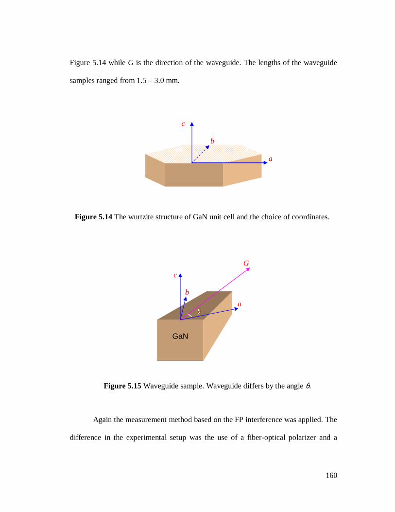
160
Figure 5.14 while G is the direction of the waveguide. The lengths of the waveguide
samples ranged from 1.5 – 3.0 mm.
Again the measurement method based on the FP interference was applied. The
difference in the experimental setup was the use of a fiber-optical polarizer and a
a
c
b
Figure 5.14 The wurtzite structure of GaN unit cell and the choice of coordinates.
G
c
b
a
GaN
Figure 5.15 Waveguide sample. Waveguide differs by the angle θ.

161
polarization controller, which are inserted immediately after the ASE source. The
experimental setup is shown in figure 5.16.
The refractive indices were measured for the signal’s optical field
perpendicular, parallel, or in a specific angle to the crystal c-axis for each sample with
a specific θ value. Figure 5.17 shows the measured optical transfer functions on a
particular waveguide sample for 15=θ . In the measurement, the input signals were
applied in three polarization states, and the relative measured results of transfer
functions are shown with the three traces in the figure. Trace 1 is for the input optical
signal polarized perpendicular to the c-axis while trace 3 is for the signal parallel to
the c-axis. For a better illustration, we have intentionally shifted the two traces by
8.0± dB based on the measured values. It can be seen that the transfer functions are
Figure 5.16 The birefringence measurement experimental setup.
Five-dimensionaladjustable stages Fixed stand
Tapered single-mode fibers
Waveguide device
Optical powermeter /opticalspectrumanalyzer
EDFA

162
typically FP-typed. It can also be seen that there is a small difference in the periods of
the two traces. This means that the effective refractive indices are slightly different
for the signals with different polarizations. Furthermore, these two traces can be
numerically fit by a normalized FP transfer function [34]:
1
02
)2/(4cos21)(
−
+
∆±−+= ϕ
λπ
λnnL
RRT eff (5.50)
Where L = 2.31 mm is the length of the waveguide; R = 3.75% is the effective round-
trip power loss of the waveguide when it acts as a FP cavity with its end surfaces
-1.5
-1
-0.5
0
0.5
1
1.5
1547 1548 1549 1550 1551 1552 1553 1554
Wavelength (nm)
Nor
mal
ized
tra
nsm
issi
on
1
2
3
Figure 5.17 Measured (solid dots) and calculated (continuous lines) optical transfer function with the input optical field perpendicular (trace 1), parallel (trace 3) and
450 from (trace 2) the crystal c-axis. (After [34])

163
acting as mirrors; and ϕ0 is the initial phase that can be determined by the best fitting
between the measured and the calculated values. If we denote n⊥ as the effective
refractive index of the waveguide when the optical field is perpendicular to the
material c-axis, and //n as the effective refractive index when the optical field is
parallel to c-axis in the waveguide, we usually get //nn ≠⊥ when birefringence exists
for the waveguide. From the numerical fitting by using equation (5.50) as shown in
figure 5.17 (the solid lines), we can obtain 357.2// =n , and 315.2=⊥n by the best
fittings, as shown in traces 1 and 3. So the refractive index difference due to the
birefringence is 042.0)( // =−=∆ ⊥nnn in this particular case. To explore where this
birefringence is from, we did a separate BPM simulation on the waveguide in figure
5.9, and found that the refractive index difference between the “⊥” and the “//”
polarization components induced by the waveguide structure is less than 10-5. This
clearly indicates that the measured ∆n value of 0.042 is primarily caused by the
material birefringence instead of the waveguide structure, which means that it is not
practical to try to overcome the birefringence by changing the structure, more
specifically, the width and the height of the waveguide.
Another measurement and fitting were also made for the input signal splitting
equally into the “⊥” and the “//” polarization modes. This is shown as trace 2 in
figure 5.17. From the figure, we could see that the ripple amplitude of the FP transfer
function has a null at wavelength 1551.2 nm. This can be explained that there is a π
phase walk-off between the TE and the TM polarization modes of that wavelength. If

164
we compare trace 1 and trace 3 in the figure carefully, we can clearly see this π phase
walk-off. It is obvious that multiple nulls can be found at different wavelengths for
this polarization state of the input signal by simply enlarging the measurement
wavelength coverage. With the information of the wavelengths at which the nulls
appear, we can determine the birefringence by [34]
)2/(20 λλ ∆=∆ Ln (5.51)
Where λ0 is the average wavelength used in the measurement, and ∆λ is the
wavelength difference between the adjacent nulls in the transfer function.
Figure 5.18 Measured birefringence versus waveguide orientation (solid squares). The continuous line is a sinusoid fitting using, ∆n = 0.04275-0.00545cos(6θ), where θ is in degree.
0.035
0.04
0.045
0.05
0 20 40 60 80 100
Waveguide orientation θ (degree)
Inde
x di
ffer
ence
∆n =
(n x
– n
y)

165
Besides that the two values of n⊥ and n// are not the same, more importantly,
we found that there is an approximately 10% change in the index difference
⊥−=∆ nnn // with varying the θ value, and also a 60o periodicity was observed.
Figure 5.18 shows this result, where systematic measurements were made on a
number of waveguide samples with angle θ = 00, 150, 300, 600 and 900. The
continuous line in figure 5.18 is the fitting curve, ∆n = 0.04275-0.00545cos(6θ),
where θ is in degree. Thus we verified that the refractive index not only depends on
the optical signal polarization but also depends on the optical propagation direction
within the a-b plane of the waveguide samples. This is attributed to the wurtzite
structure of the GaN crystal.
Although the above periodical variation of ∆n within c-plane was obtained in
the infrared wavelengths, we can assume that this 60o periodicity in ∆n variation also
exists in the wavelength regions near the band edge based on the fact that the
periodical emission-efficiency variation versus angleθ in c-plane has been reported in
[70].
For most applications of planar lightwave circuits, the birefringence of the
waveguide is an important issue that has to be considered. Less birefringence in the
waveguides guarantees better real communication systems. Several techniques have
been proposed to reduce the birefringence in the waveguides made by semiconductor
materials. Those techniques include polarization compensation [71]; special
waveguide cross-section design [72][73]; and the introduction of build-in
compressive, or tensile stresses during the crystal growth [74][75].

166
The measured result given above gives us a foundation for the design of the
polarization insensitive waveguide with the technique of special cross-section design.
Since there are two types of birefringence: the material birefringence and the
waveguide birefringence, it is important to consider both of them in the designing.
Through simulation, we could design some specific waveguide birefringence in the
waveguide design based on the chosen refractive indices. Then, we can carefully
choose the direction of the incident beam to have some specific material
birefringence. If these two types of birefringence compensate for each other, a
polarization insensitive waveguide can be realized.
5.7 Design of Optical Couplers and Mach-Zehnder Interferometer Device
with GaN/AlGaN
In Chapter 2, we discussed the principles of basic devices such as couplers,
Mach-Zehnder Interferometers. In this section, we are going to design functional
devices with GaN materials.
Figure 5.19 Simulation of a 3dB coupler.

167
5.7.1 Simulation Results of Couplers and Mach-Zehnder Interferometer Device
The simulation results for our designing of simple 2 × 2 waveguide couplers
and Mach-Zehnder Interferometers are shown here. Figure 5.19 shows a simulation
result for a 2 × 2 3-dB waveguide coupler. The input power from one of the input
ports of the coupler was split equally to the two output ports.
Figure 5.20 shows the simulation result where a Mach-Zehnder Interferometer
acted as a simple optical switch. In the simulation, the length difference ∆L between
the two arms was realized by having different refractive indices in the waveguides of
the two arms. This can be made by having an electrode on one of them. In our
simulation, the refractive index difference between the two arms was set as 0.0238.
The signals with different wavelengths 1.5464 µm and 1.5625 µm were launched into
the same input port. But they exit from different output ports. This simulation was set
2
1
Figure 5.20 Simulation of M-Z Interferometer optical switch controlled by carrier induced refractive index change.

168
for the design of optical switches that could be realized with carrier induced refractive
index change.
Figure 5.21 Microscopic images of a 2×2 GaN/AlGaN heterostructure optical waveguide coupler (a) top view and (b) cross section at the output. (Ref. [29])
1 2
3
4
(a)
(b)

169
5.7.2 A Simple Example: Waveguide Coupler
The first samples we designed have the waveguide widths all equal to 3µm.
Several different waveguide configurations were designed and fabricated. The
devices included straight waveguides and 2 × 2 waveguide couplers.
Figure 5.21 shows an example of a fabricated device samples based on our
design. It is a typical 2 × 2 optical waveguide coupler [29]. The power splitting ratio
Figure 5.22 Measured output optical power vs the probe displacement in the horizontal direction for a 2×2 GaN/AlGaN heterostructure optical waveguide coupler.
The input optical signal is launched at port 1 (as illustrated in Fig. 3-6) (Ref [29]).
-40 -20 0 20 40
Out
put
pow
er (
linea
r sc
ale)
Probe displacement (µm)
Port 3
Port 4

170
of this particular coupler was designed to be 3dB. To characterize the sample, the
experimental setup was the same as shown in figure 5.11, except that a tunable laser
was used to replace the EDFA. The result is shown in figure 5.22, where the output
powers were measured at the two outputs (3 and 4) while the input power was from
input port 1. From figure 5.22, we see that the experiment result is in accordance with
our design. A ∼50% power splitting was realized.
5.8 The AWG Based on the GaN/AlGaN Heterostructures
In chapter 2, we have discussed the basic principles of an AWG. In chapter 3,
the AWG was used as the basic component to construct an IAWG and IAWG-based
WDM cross connects or all optical switches. In this section, we are going to show the
design of an AWG with GaN/AlGaN materials. We will also explain the reason why
we have chosen GaN/AlGaN instead of other materials.
One approach to make the AWG devices is to use the silica PLC, which is the
most popular one, and the AWGs made in this way are commercially available now.
However, AWG devices made of silica are usually not tunable due to the passive
nature of silica. One approach to make the AWG tunable to make wavelength
switches is by using thermal tuning method [76][77]. The thermal tuning method has
been briefly discussed in chapter 2, for thermo-optic Mach-Zehnder Interferometer
(MZI) switch, and in the introduction part of chapter 3. In the AWG case, a small
resistor is deposited near each arrayed waveguide. This small resistor can heat the

171
related waveguide individually to change its refractive index, so that a relative optical
delay is introduced in the waveguide. However, as we have pointed out in chapter 2,
this method is very slow since it is in millisecond level. It cannot be applied to the
packet switch-based optical networks. Another approach is to use semiconductor
materials to make planar waveguide PLCs. Since InP is semiconductor, the InP-based
PLC can be potentially made fast tunable with the carrier injection [6][8]. However,
there are also several disadvantages with the InP-based devices. Firstly, it has too
high refractive index ( 5.3≈n ) compared with silica. The cross-section of the
waveguide made of InP is very small, which causes extra coupling loss at the
interface with an optical fiber, due to the refractive index mismatch, and due to the
mode spot size mismatch. Secondly, the temperature sensitivity of the refractive
index of InP material is very high, which is 1410/ −−≈ KdTdn , which is
approximately 10 times higher than that of silica. So the performance of the InP-
based AWG devices is very sensitive to the temperature change, and the stringent
temperature control is required. This has become part of the reason why the InP-based
AWG devices have not become commercially competitive so far.
Compared with InP and Silica, the III-nitrides have distinct advantages for the
application of tunable AWG optical devices. The lower refractive index than InP
makes the waveguide cross section larger than that of InP waveguide, which reduces
the coupling loss with optical fibers significantly. The wide bandgap relative to the
application wavelength 1550 nm makes the intrinsic loss and optical gain small. On
the other hand, its semiconductor characteristic makes it possible to change its

172
refractive index by carrier injection, primarily by free carrier absorption in this case
as we have discussed in chapter 4. This makes it possible to design fast tunable
AWG devices.
5.8.1 Simulation Results of the Arrayed Waveguide Gratings
Based on the previous simulations, another waveguide device, arrayed
waveguide grating (AWG) on GaN and AlxGa1-xN was then designed and simulated.
Figure 5.23 shows this AWG configuration (a), and the related simulation result (b).
The size of the AWG configuration was about 5.5 × 8.8 µm2. It consisted of one input
star coupler with one input port, one output star coupler with eight output ports, and
40 arrayed waveguides between the two star couplers. The waveguide had the same
layered structure as in Figure 5.9. The simulation result was in accordance with what
we had expected. Each of the eight output ports had its specific peak wavelength for
the output signal.

173
Figure 5.23 (a) Arrayed waveguide grating configuration, (b) simulation output result.
(a)

174
5.8.2 A Sample: A Fabricated Arrayed Waveguide Grating
To verify the feasibility, a GaN/AlGaN-based AWG was fabricated for the
first time based on the simulation result as shown above. The fabrication procedure
was identical to that described in section 5.3.3.3, which involved photolithographic
patterning and inductively-coupled plasma (ICP) dry etching [65]. Figure 5.24 shows
a sample of an AWG-based 1 × 8 WDM demultiplexer. Figure 5.24(a) is a
microscope picture of the device configuration, which consists of one input
Figure 5.23 (b)

175
waveguide, eight output waveguides, two star couplers, and 40 arrayed waveguides
between the two star couplers. By design, the channel spacing of the WDM outputs is
2 nm. Figure 5.24(b) shows the measured optical transfer function versus the signal
wavelength for all the eight output ports. It can be seen that the measured transfer
function of the AWG generally agrees with the simulated one as shown in figure
5.23(b). The results clearly demonstrated an approximately 2 nm wavelength spacing
between transmission peaks of adjacent output waveguides. This indeed verifies the
accuracy of the design. It is noticed that the out-of-band rejection ratio of the
measured transfer function is only approximately 10 at most of the output ports. This
is mainly due to the non-uniformity of the waveguide array caused by the
imperfections in the fabrication process.

176
Input
Star couplers Waveguide array
Outputs
(a)
Figure 5.24 Microscope picture (a) and measured optical transfer function (b) of an AWG-based WDM coupler with 2nm channel separation.

177
5.9 The Thermal Stability of the Refractive Index
The dependence of the refractive index of AlxGa1-xN on temperature has been
investigated extensively [78]. Although previous research has been focused on the
characteristics of AlxGa1-xN in UV and visible wavelength region, the theoretical
formulation can be extended into near the infrared region. We adopt the expression of
the refractive index as the function of temperature, wavelength and Al concentration
for AlxGa1-xN in [78]:
Wavelength (nm)
0
0.2
0.4
0.6
0.8
1
1545 1547 1549 1551 1553 1555 1557 1559
Nor
mal
ized
Tra
nsm
issi
on (
a.u.
)
Figure 5.24 (b)

178
2/122
2
1),,( irrTxn εεελ ++= (5.52)
Where εr and εi are the real and the imaginary parts of the dielectric constant ε,
respectively, with,
25.1
112
),(
),(),(),,(
y
yy
TxE
TxATxCTx
g
−−+−⋅+=λε (5.53)
),(
),(/
TxE
Txihcy
g
Γ+= λ (5.54)
1)/386.0exp(
224.099.035.1502.3),( 2
−−++=
TxxTxEg (5.55)
3 6 2
3 6 2
( , ) 2.49 2.27 10 1.8 10
(0.74 4.61 10 5.33 10 )
C x T T T
T T x
− −
− −
= + × − ×− + × − ×
(5.56)
2 5 2
4 2 1.5
( , ) 79.3 8.37 10 6.73 10
(18.99 0.13 1.76 10 ) [ ]
A x T T T
T T x eV
− −
−
= − × − ×
+ + − × (5.57)
][10)19.024.248(1013.469.8),( 322 eVxTTTx −− ×−+×+−=Γ (5.58)
This approximation is valid for the Al concentration x < 0.64 and the accuracy
was tested against the measured data obtained with a spectroscopic ellipsometor
between 3.5 eV and 1.5 eV (850nm wavelength). Although the accuracy of this
equation in the 1550 nm wavelength region has not been fully verified, at this
wavelength that is far away from the material bandgap, no abrupt variation is
expected for the material characteristics. Equations (5.52)-(5.58) will provide a

179
reasonably accurate estimation for the temperature sensitivity of the refractive index
at 1550 nm. Figure 5.25 (a) shows the sensitivity of the refractive index against the
temperature change (dn/dT ) at the wavelength of 1550 nm with various values of Al
concentration x. Within 0 and +50 oC, the temperature sensitivity is less than
C/102 5−× . This value is similar to that of silica [54], and approximately one order
of magnitude lower than that of InP, which is about C/103 4−× [55][56] at this
wavelength. It is interesting to note that for AlxGa1-xN at room temperature (25 oC),
the temperature sensitivity of the refractive index is not monotonic versus Al
concentration x, as shown in Figure 5.25(b), which shows a maximum around x = 0.4.

180
Figure 5.25 Calculated temperature sensitivity of AlGaN refractive index, (a) as a function of operation temperature for different Al concentration x and, (b) as a
function of Al concentration with a fixed operating temperature at 25oC.
Inde
x ch
ange
per
o C
(dn
/dT
) x 1
0-5
Temperature (oC)
x = 0
0.4
0.2
0.8
(a)

181
Al concentration x
T = 25oC In
dex
chan
ge p
er o C
(dn
/dT
) x 1
0-5
Figure 5.25 (b)

182
6. Conclusions and Future Work
6.1 Conclusions
In this dissertation, we have reviewed the basic concepts of
telecommunication network architectures, optical networks, WDM network elements,
and basic components in optical networks. Among the basic components, we have
particularly focused on the basic principles and applications of optical couplers,
Mach-Zehnder Interferometers (MZI), and arrayed waveguide gratings (AWG). In
terms of large optical switch architectures, we have emphasized our interest in the
Spanke architecture. Then we reviewed a number of popular switch device
technologies, such as MEMS and thermo-optic switches. The MEMS technique has
inspired us to build 1 × N optical switches to realize N × N with the Spanke
architecture. The thermo-optic technique has inspired us to explore the possibility of
using carrier-induced semiconductor material to realize the switching of optical
signals with particular wavelengths.
Our main focus has always been on all-optical switching in WDM technology.
We have explored and invented a novel structure for an all-optical switch in Chapter
3. We started with the basic AWG design and expanded it into the N-interleaved
AWG (N-IAWG). Compared to a conventional AWG, an N-IAWG requires a unique
differential path length design in the bridge waveguides between the two star couplers.
We derived a general design rule for the required differential lengths of bridge
waveguides in an N-IAWG. We discovered that there exist multiple solutions to the

183
differential path lengths in the N-IAWG design. Based on this, we designed and
systematically analyzed a 1 × N WDM switch, which consists of two N-IAWGs with
a phase shifter array between them. A practical design example of a 1 × 4 non-
blocking WDM switch was then presented to illustrate the design steps and the
methods to find the required phase assignment at each phase shifter for various output
status. We also calculated the device transfer functions and discussed the switching
functionalities in detail. Based on the reciprocity principle, we also proposed a
simplified structure of a 1 × N WDM switch that requires only one N-IAWG, where
total reflection is implemented at the end of each phase shifter. This simplified
structure significantly reduces the device size and relaxes the design tolerance. It is
also important to note that the proposed 1 × N switch structure is a PLC with no
waveguide crossings, therefore it can be monolithically integrated to create
sophisticated optical devices with various functionalities. We can use this type of 1 ×
N WDM switches as fundamental building blocks to construct non-blocking N × N
WDM all-optical switches, which we have also suggested in this dissertation and
which will be indispensable for future all-optical networks.
The feasibility of incorporating carrier-induced index tuning into switchable
PHASAR devices depends on the characteristics of semiconductors. Therefore, it is
important to find proper materials to realize our unique designs. We proposed to use
III-nitrides because of their unique characteristics. We presented a theoretical study of
carrier-induced refractive index change in GaN semiconductors in the infrared
wavelength region, which was previously not well-known. The results of this study

184
provide us critical material parameters for switchable phasor device designs for
optical communication applications. In our approach, we have studied three carrier
effects: band filling, bandgap shrinkage, and free-carrier absorption. The results
indicate that in infrared wavelengths, the dominant cause of carrier-induced refractive
change is due to free-carrier absorption. Through our calculation, we verified that the
magnitude of carrier-induced refractive change is high enough for future applications
as PHASAR devices for optical communications. The devices we proposed are
feasible with GaN materials.
We then characterized the optical properties of AlxGa1-xN epilayers in the
1550 nm wavelength region experimentally, including the refractive indices and the
impact of Al concentrations. We designed various functional optical devices based on
the single-mode ridged optical waveguides using GaN/AlGaN heterostructures. The
devices were then systematically characterized for their operation in the 1550 nm
wavelength window. We observed and studied the birefringence of wurtzite GaN
grown on sapphire substrate. We found that the refractive indices were different for
the signal optical field perpendicular and parallel to the crystal c-axis ( //nn ≠⊥ ).
More importantly, we found an approximately 10% change in the index difference
⊥−=∆ nnn // when varying the waveguide orientation within the c-plane, with a 60o
periodicity. This is attributed to the hexagonal structure of the nitride materials. This
knowledge will help the understanding of polarization effect in the devices and the
design of polarization independent optical waveguides. An 8-wavelength array-
waveguide grating was designed and fabricated using III-nitride semiconductor

185
materials for the first time. The performance reasonably agrees with our design
expectation, which indicates that we have good understanding of the material
properties as well as device design rules. We have also investigated the thermal
sensitivity of the refractive index of AlGaN in the 1550 nm wavelength region, which
has been found comparable to that of silica and approximately one order of
magnitude lower than that of InP.
6.2 Future Work
This report has demonstrated our work in three areas of all-optical switching:
high level schematic designs; device structural calculations and simulations; and
experimental testing and verification. Although a foundation has been formed, there
is still plenty of room for future research in these three areas.
• New schematic designs can still be explored. For example, a ring resonator
can be used for demultiplexing or multiplexing filters. It can also be applied to
configure multiplexer by using multiple resonators [41].
• We have measured the birefringence of GaN materials. However, it still
remains a task to practically design polarization insensitive waveguides in
integrated optical circuits. The techniques include a careful choice of an angle
between a-axis and the waveguide direction in the photonic circuit design. A
special cross-section design of waveguide and an introduction of built-in
stresses in the crystal structure are worth further exploring.
• Carrier-induced refractive index changes in the GaN rectangular waveguide
have been theoretically explored and calculated. Devices designed using

186
theoretical calculations and simulations have been recently fabricated. The
remaining work in this area is to experimentally measure the carrier-induced
refractive index change. There are two ways to improve in this part. One way
is to improve the sample preparation process so that we could have an ideal F-
P cavity so the experimental method introduced in Chapter 5 can still be
applied to measure the refractive index change. The other way is to develop
novel methods to do the measurement. We have already started to try some
new methods. For example, we started using a fabricated MZI device with
electrodes attached to verify the results experimentally. It can be seen that
either way is challenging.
• Besides the experimental verification of carrier-induced refractive index
change, the design and location of the electrodes on or near optical waveguide
also remains to be explored. We will then have a solid foundation to fabricate
and characterize the active optical devices we proposed in this dissertation.
• After the verification of the carrier-induced refractive index change
experimentally, a series of measurements needs to be taken to measure the
effective refractive index changes with different carrier concentrations in
waveguide samples. Then we can compare the experimental results with the
theory to verify some key parameters we had chosen in the theoretical
calculations.
• A thorough research in the mechanism of optical power loss needs to be
carried out. For example, losses could be due to coupling to radiation modes

187
or due to scattering [41]. Understanding this loss mechanism could help us to
design low loss waveguides. For example, we can reduce the loss due to
scattering by using geometries that can minimize the mode overlap with the
rough sidewalls of the waveguide [41].
• There are some approximations we made when investigating temperature
sensitivity of the refractive index for GaN materials. This temperature
characteristic needs to be verified experimentally.
• Recently, silicon has been widely investigated and applied as a new material
for optical devices due to the recent realization of sub-micrometer-size
photonic structures [41][79]. Besides the channel waveguides and ridge
waveguides, novel waveguide configurations such as photonic-crystal
waveguides and slot waveguides have also been proposed [41]. Because of the
high refractive index of silicon, confined bent waveguides with small radii can
be realized. Although there is a big difference between the materials of Silicon
and III-Nitrides, the basic principles in theory, in architecture designs, and in
experimental methods are very similar. Therefore we can extend our research
method presented in this dissertation into silicon applications in optical
telecommunications.

188
7. Bibliography
[1] Rajiv Ramaswami and Kumar N. Sivarajan, Optical Networks, A Practical
Perspective, 2nd Ed, Academic Press, San Francisco, 2002.
[2] R.P. Khare, Fiber Optics and OptoElectronics, Oxford University Press, New
Delhi, 2004.
[3] Gerd Keiser, Optical Fiber Communications 3rd Ed, (McGraw-Hill, Boston, 2000).
[4] M. F. Dautartas, A. M. Benzoni, Y. C. Chen and G. E. Blonder, “A Silicon-based
moving-mirror optical switch,” IEEE/OSA Journal of Lightwave Technology, Vol.
10, pp. 1078-1085, 1992
[5] L. Y. Lin, E. L. Goldstein, J. M. Simmona and R. W. Tkach, “Free-space
micromachined optical switches with submillisecond switching time for large-
scale optical crossconnects,” IEEE Photonics Technology Letters, Vol. 10, pp.
525-527, 1998.
[6] C. R. Dorr, C. H. Joyner, L. W. Stulz and R. Monnard, “Wavelength-division
multiplexing cross connect in InP,” IEEE Photonics Technology Letters, Vol. 10,
pp. 117-119, 1998.
[7] C. G. P. Herben, D. H. P. Maat, X. J. M. Leijtens, M. R. Leys, Y. S. Oei and M. K.
Smit, “Polarization independent dilated WDM cross-connect on InP,” IEEE
Photonics Technology Letters, Vol. 12, pp. 1599-1601, 1999

189
[8] M. K. Smit and C. van Dam, “PHASAR-based WDM-devices: Principles, design
and applications,” IEEE Journal of Selected Topics in Quantum Electronics, Vol.
2, No. 2, pp. 236-250, 1996.
[9] S. Nakamura and G. Fasol, The blue laser diodes, (Springer-Verlag, Berlin,
Heidelberg, New York, 1997).
[10] Nitride News, Compound Semiconductor, Vol.3, page 4, 1997.
[11]S. Taherion, R. Hui and K. Nordheden, M. Goano, A. Baldanzi, and H. X. Jiang
“Experimental and theoretical study of refractive indices of wurtzite GaN thin
film from visible to infrared,” Integrated Photonics Research Conference,
Monterey, California, June 13 –15, 2001
[12] Luying Zhou, et al, “Development of a GMPLS-Capable WDM optical network
testbed and distributed storage application”, IEEE Communications Magazine, vol.
44, issue 2, pp. 23 - 29, 2006.
[13] Guangzhi Li; Dongmei Wang; Yates, J.; Doverspike, R.; Kalmanek, C, “Detailed
study of IP/ reconfigurable optical networks”, Broadband Networks, 2004.
BroadNets 2004. Proceedings. First International Conference, pp. 64-73, 2004.
[14]Kyeong Soo Kim, et al, “Design and Performance Analysis of Scheduling
Algorithms for WDM-PON Under SUCCESS-HPON Architecture”, IEEE
Journal of Lightwave Technology, vol. 23, pp.3716-3731, 2005.
[15] Yikai Su, et al, “A Multirate Upgradeable 1.6-Tb/s Hierarchical OADM
Network”, IEEE Photonics Technology Letters, vol. 16, pp.317-319, 2004.

190
[16] Zhaoxin Wang, Chinlon Lin, and Chun-Kit Chan, “Demonstration of a Single-
Fiber Self-Healing CWDM Metro Access Ring Network With Unidirectional
OADM”, IEEE Photonics Technology Letters, vol. 18, pp.163-165, 2006.
[17] Michael Vasilyev, et al, ““Broadcast and Select” OADM in 80 × 10.7 Gb/s
Ultra-Longhaul Network”, IEEE Photonics Technology Letters, vol. 15, pp.332-
334, 2003.
[18]June-Koo Rhee, Ioannis Tomkos, and Ming-Jun Li, “A Broadcast-and-Select
OADM Optical Network With Dedicated Optical-Channel Protection”, IEEE
Journal of Lightwave Technology, vol. 21, pp.25-31, 2003.
[19]A. Yariv, Optical Electronics in Modern Communications, Oxford University
Press, 1997.
[20]H. Takahashi, K, Oda, H. Toba, Y. Inoue, “Transmission Characteristics of
Arrayed Waveguide N × N Wavelength Multiplexer”, J. of Lightwave, Technol.,
vol. 13, pp. 447-455, March 1995.
[21] “What is MEMS Technology?”
URL: http://www.memsnet.org/mems/what-is.html
[22]C. Dragone, “An N × N optical multiplexer using a planar arrangement of two
star couplers,” IEEE Photon. Technol. Lett. vol. 3, pp. 812-815, Sept. 1991.
[23]C. Dragone, C. A. Edwards, and R. C. Kistler, “Integrated optics N × N
multiplexer on silicon,” IEEE Photon. Technol. Lett. vol. 3, pp. 896-899, Oct.
1991.

191
[24]Y. Tachikawa, Y. Inoue, M. Kawachi, H Takahashi, and K. Inoue, “Arrayed-
waveguide grating add-drop multiplexer with loop-back optical paths,” Electron.
Lett., vol. 29, pp. 2133-2134, Nov. 1993.
[25]H. Takahashi, O. Ishida, K. Oda and H. Toba, “Anticrosstalk arrayed-waveguide
add-drop multiplexer with foldback paths for penalty free transmission,” Electron.
Lett., vol. 30, pp. 2053-2055, Nov. 1994.
[26]S. Matsuo, Y. Yoshikuni, T. Segawa, Y. Ohiso and H. Okamoto, “A Widely
Tunable Optical Filter Using Ladder-Type Structure,” IEEE Photon. Technol. Lett.
vol. 15, pp. 1114-1116, Aug. 2003.
[27]C. R. Doerr, “Proposed WDM Cross Connect Using a Planar Arrangement of
Waveguide Grating Routers and Phase Shifters,” IEEE Photon. Technol. Lett. vol.
10, pp. 528-530, Apr. 1998.
[28]C. R. Doerr, C. H. Joyner, L. W. Stulz, and R. Monnard, “Wavelength-Division
Multiplexing Cross Connect in InP,” IEEE Photon. Technol. Lett. vol. 10, pp.
117-119, Jan. 1998
[29] R. Hui, et al, “GaN-based waveguide devices for long-wavelength optical
communications”, Appl. Phys. Lett., vol. 82, 1326(2003).
[30]Ivan Kaminow, Tingye Li, Optical Fiber TelecommunicationsIV A Components,
Chapter 9, Academic Press, San Diego, 2002.
[31]BeamPROP AWG Utility Version 2.1, Rsoft, Inc. Research Software.
[32] C. Dragone, “Optimum design of a planar array of tapered waveguides,” J. Opt.
Soc. Amer.A. vol. 7, pp. 2081-2091, 1990.

192
[33]K. Okamoto, Fundamentals of Optical Waveguides, Academic Press, 2000
[34]R. Hui, et al, “III-Nitride-Based Planar Lightwave Circuits for Long Wavelength
Optical Communications”, IEEE J. Quantum Electron., vol. 41, no. 1, pp.100-110,
Jan, 2005.
[35]B. R. Bennett, Richard A. Soref, Jesús A. Edl Alamo, “Carrier-Induced Change
in Refractive Index of InP, GaAs, and InGaAsP”, IEEE J. Quantum Electron., vol.
26, pp.113-122, 1990.
[36]K. Ishida, H. Nakamura, H. Matsumura, T. Kadoi, and H. Inoue, “InGaAsP/InP
optical switches using carrier induced refractive index change,” Appl. Phys. Lett.,
vol. 50, pp.141-142, 1987.
[37]W. Kowalsky and K. J. Ebeling, “Optically controlled transmission of InGaAsP
epilayers,” Opt. Lett., vol. 12, pp. 1053-1055, 1987.
[38] J. G. Mendoza-Alvarez, R. H, Yan and L. A. Coldren, “Contribution of the band-
filling effect to the effective refractive-index change in double-heterostructure
GaAs/AlGaAs phase modulators,” J. Appl. Phys., vol. 62, pp. 4548-4553, 1987.
[39] J. G. Mendoza-Alvarez, L. A. Coldren, A. Alping, R. H, Yan, T. Hausken, K.
Lee, and K. Pedrotti, “Analysis of depletion edge translation lightwave
modulators,” J. Lightwave Technol., vol. 6, pp 793-808, 1988.
[40] J. Manning, R. Olshansky, and C. B. Su, “The carrier-induced index change in
AlGaAs and 1.3 µm InGaAsP diode lasers,” IEEE J. Quantum Electron., vol. QE-
19, pp 1525-1530, 1983.

193
[41] Michal Lipson, “Guiding, Modulating, and Emitting Light on Silicon—
Challenges and Opportunities,” J. Lightwave Technol., vol. 23, pp 4222-4238,
2005.
[42] E. Burstein, “Anomalous optical absorption limit in InSb” Phys. Rev., vol. 93, pp
632-633, 1954.
[43] T. S. Moss, G. J. Burrell, and B. Ellis, Semiconductor Opto-electronics. New
York: Wiley, 1973, pp 48-94.
[44]B. R. Bennett, Richard A. Soref, “Electrorefraction and electroabsorption in InP,
GaAs, GaSb, InAs, and InSb”, IEEE J. Quantum Electron., vol. QE-23, pp.2159-
2166, 1987.
[45]A. Yariv, Optical Electronics, 3rd ed. New York: Holt, Rinehart and Winston,
1985, pp. 474-478.
[46]E. Michael, et al, Properties of Advanced Semiconductor Materials, GaN, AlN,
InN, BN, SiC, SiGe, John Wiley & Sons, Inc., New York, 2001.
[47]J. F. Muth, J. H. Lee, I. K. Shmagin, R. M. Kolbas, H. C. Casey, Jr., B. P. Keller,
U. K. Mishra, and S. P. DenBaars, “Absorption coefficient, energy gap, exciton
binding energy, and recombination lifetime of GaN obtained from transmission
measurements,” Appl. Phys. Lett. 71, 18(1997), 2572-2574.
[48] J. D. Dow and D. Redfield, “Toward a unified theory of Urbach’s rule and
exponential absorption edges,” Phys. Rev. B, vol. 5, pp. 594-610, 1972.

194
[49] C. H. Henry, R. A. Logan, and K. A. Bertness, “Spectral dependence of the
change in refractive index due to carrier injection in GaAs lasers,” J. Appl. Phys.,
vol. 52, pp. 4457-4461, 1981.
[50]Shun Lien Chuang, Physics of Optoelectronic Devices, John Wiley & Sons, New
York, 1995.
[51]E. A. J. Marcatili, “Dielectric rectangular waveguide and directional coupler for
integrated optics,” Bell Syst. Tech. J. 48, 2071-2102 (1969)
[52]E. A. J. Marcatili, “Slab-coupled waveguides,” Bell Syst. Tech. J. 53, 645-674
(1974)
[53]Katsunari Okamoto, Fundamentals of Optical Waveguides, ACADEMIC PRESS,
San Diego, 2000.
[54]M. Levy, L. Eldada, R. Scarmozzino, R.M. Osgood, Jr., P.S.D. Lin, and F. Tong,
“Fabrication of Narrow-Band Channel-Dropping Filters”, IEEE Photon. Technol.
Lett. vol. 4, p. 1378, 1992.
[55]L. Eldada, M. N. Ruberto, M. Levy, R. Scarmozzino, and R. M. Osgood, Jr.,
“Rapid Direct Fabrication of Active Electro-Optic Modulators in GaAs”, J.
Lightwave Tech.,. vol. 12, p. 1558, 1994.
[56]I. Ilic, R. Scarmozzino, R.M. Osgood, Jr., J.T. Yardley, K.W. Beeson, and M.J.
McFarland, “Modeling Multimode-Input Star Couplers in Polymers”, J.
Lightwave Tech., vol. 12, p. 996, 1994.
[57]I. Ilic, R. Scarmozzino, R.M. Osgood, Jr., J.T. Yardley, K.W. Beeson, and M.J.
McFarland, and J. Schweyen, “Photopattermed Polymer Multimode 8x8 Star

195
Couplers: Comparative Design Methodologies and Device Measurements”, IEICE
Trans. Commun., vol. E80-B, 1997.
[58] L. Eldada, R. Scarmozzino, R.M. Osgood, Jr., D.C. Scott, Y. Chang, and H.R.
Fetterman, “Laser-Fabricated Delay Lines in GaAs for Optically-Steered Phased-
Array Radar”, J. Lightwave Tech., vol. 13, p. 2034, 1995.
[59] M.H. Hu, Z. Huang, K.L. Hall, R. Scarmozzino, and R.M. Osgood, Jr., “An
Integrated Two-Stage Cascaded Mach–Zehnder Device in GaAs”, J. Lightwave
Tech., vol. 16, pp. 1447-1455, 1998.
[60]M. Hu, R. Scarmozzino, M. Levy, and R.M. Osgood, Jr., “A low-loss and
compact waveguide y-branch using refractive index tapering”, Photon. Tech. Lett.,
vol. 9, pp. 203-205, 1997.
[61] R. Scarmozzino, R.M. Osgood, Jr., L. Eldada, J.T. Yardley, Y. Liu, J. Bristow, J.
Stack, J. Rowlette, and Y.S. Liu, “Design and Fabrication of Passive Optical
Components for Multimode Parallel Optical Links”, SPIE Photonic West Meeting,
San Jose, CA, vol. 3005, p. 257, 1997.
[62] M. Hu, J.Z. Huang, R. Scarmozzino, M. Levy, and R.M. Osgood, Jr., “Tunable
Mach-Zehnder polarization splitter using height-tapered y-branches”, Photon.
Tech. Lett., vol. 9, pp. 773-775, 1997.
[63] J. Fujita, M. Levy, R. Scarmozzino, R.M. Osgood, Jr., L. Eldada, and J.T.
Yardley, “Integrated Multistack Waveguide Polarizer”, Photon. Tech. Lett., vol.
10, pp. 93-95, 1998.
[64] BeamPROPTM Version 5.0, Rsoft, Inc

196
URL: http://www.rsoftinc.com
[65] T. N. Oder, J. Y. Lin and H. X. Jiang, “Propagation properties of light in
AlGaN/GaN quantum-well waveguides,” Applied Physics Letters, Vol. 79, pp.
2511-2513, 2001
[66]Max Ming-Kang Liu, Principles and Applications of Optical Communications,
McGraw-Hill, Inc., Chicago, 1996.
[67] K. B. Nam, J. Li, M. L. Nakarmi, J. Y. Lin, and H. X. Jiang, "Achieving highly
conductive AlGaN alloys with high Al contents," Appl. Phys. Lett. Vol. 81, pp.
1038-1040, 2002.
[68]V. Fiorentini, F. Bernardini, F. Della Sala, A. Di Carlo and P. Lugli, “Effects of
macroscopic polarization in III-V nitride multiple quantum wells”, Phys. Rev. B,
60, 8849, (1999)
[69]S. Ghosh, P. Waltereit, O. Brandt, H. T. Grahn and K. H. Ploog, “ Polarization-
dependent spectroscopic study of M-plane GaN on γ-LiAlO2”, Appl. Phys. Lett.
80, 413 (2002)
[70]T. N. Oder, J.Y. Lin and H.X. Jiang, “Fabrication and Optical Characterization of
III-Nitride Sub-micron Waveguides,” Appl. Phys. Lett., vol. 79, pp. 12-14, 2001
[71]M. Zirngibl, C. H. Joyner and P. C. Chou, “Polarization compensated waveguide
grating router on InP,” IEE Electronics Letters, Vol. 31, No. 19, pp. 1662-1664,
1995.

197
[72] H. Bissessur, P. Pagnod-Rossiaux, R. Mestric, and B. Martin, “Extremely small
polarization independent phased-array demultiplexers on InP,” IEEE Photonics
Technology Letters, Vol. 8, No. 4, pp. 554-556, 1996.
[73] J. Sarathy, S. Chandrasekhar, A. D. Dentai, and C. R. Doerr, “Polarization
insensitive waveguide grating routers in InP,” IEEE Photonics Technology Letters,
Vol. 10, No. 2, pp.
[74] IEEE J. Quantum Electronics, Special Issue on Strained-layer Optoelectronic
Materials and Devices, Vol. 30, No. 2, 1994.
[75] T. Kakitsuka, Y. Shibata, M. Itoh, Y. Kadota, Y. Tohmori and Y. Yoshikuni,
“Influence of buried structure on polarization sensitivity in strained bulk
semiconductor optical amplifiers,” IEEE J. Quantum Electronics, Vol. 38, No. 1,
pp. 85-92, 2002.
[76] M. Okuno, K. Kato, Y. Ohmori, M. Kawachi and T. Matsunaga, “Improved 8x8
integrated optical matrix switch using silica-based plannar lightwave circuits,”
IEEE/OSA Journal of Lightwave Technology, Vol. 12, pp. 1597-1605, 1994.
[77] N. Takato, T. Kominato, A. Sugita, K. Jingugi, H. Toba and M. Kawachi,
“Silica-based integrated optical Mach-Zehnder multi/demultiplexer family with
channel spacing of 0.01 – 250nm,” IEEE Selected areas in Communications, Vol.
8, No. 6, pp. 1120-1127, 1990.

198
[78] U. Tisch, B. Meyler, O. Katz, E. Finkman and J. Salzman, “Dependence of the
refractive index of AlxGa1-xN on temperature and composition at elevated
temperatures,” J. Appl. Phys., Vol. 89, No. 5, pp. 2676-2685, 2001.
[79] R. C. Johnson. (2002). “Intel reveals long-term goals for silicon photonics,
sensors,” Electron. Eng. Times. Available:
http://www.eetimes.com/semi/news/OEG20020228S0033


